

Page 1

Operator’s Manual
Model 181
Digital Nanovoltmeter
01982. Keithley Instruments, Inc
Cleveland, Ohio, U.S.A.
Document Number 32421
Page 2
181
l
NANOVOLTMETER
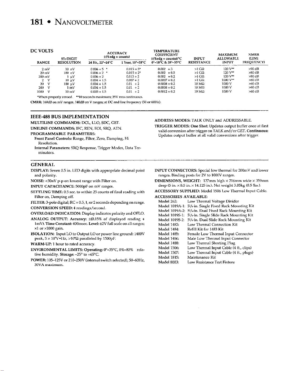
IEEE-488 BUS IMPLEMENTATION
MULTlLlNE COMMANDS: DCL, LLCJ, xc, GET.
“NlLINE COMMANDS: IFC, REN, EOI, SRQ, ATN.
PROGRAMMABLE PARAMETERr3
Front Panel Controls: Range, Filter, Zero, Damping, Hi
Resoluli”“.
Internal Pnrametea: SRQ Rcsponsc, Trigger Modes, Data Ter-
minators.
GENERAL
DISPLAY: Seven 0.5 in. LED digits with appropriate decimal point
and polarity.
NOISE: <30”” p-p on lowest range wit,, Filter on.
lNP”T CAPACITANCE: 5OOOpF on mV ranges.
SETTLING TIME: 0.5 sec. to within 25 COLMS of final reading with
Fikr on, Damping off.
FILTER: 3-polcdigital; RC = 0.5.l.or2 wands dcpcndingonrangc.
CON”CRSlON WEBI): 4 readings/second.
OVERLOAD INDICATION: Display indicates polarity and OFI.0.
ANALOG OUTPUT: Accuracy: +(0.15% of displayed reading +
ImW Time Constant: 400mscc. Level: f2V full scale on all rongcs;
xl or xl000 gain.
ISOLATION: Input LO to Output LO or power line ground: ,400”
peak, 5 x IOW*Hz, >I09 paralleled by 150OpF.
WARM-UP: 1 hour to r&cd accuracy.
ENVIRONMENTAL LIMITS: Operating: 0”35”C, O%-80% *da-
tive humidity. Storage: -25” to +WC.
POWER: 105-123’ or 21~25OV (internal switch selected), 50-6OHz,
30Vh maximum.
ADDRESS MODES: TALK ONLY and ADDRESSABLE.
TRIGGlX MODES: One Shot: Updatcs output buffer once at first
valid conversion after triggeronTALKand/arG~T. Continuous:
Updates output buffer at al, valid ~onwr~ion~ after trigger.
INFUT CONNECTOR% Special low thermal for 2”OmV and lower
ranges. Binding posts for 2V to lOO”V ranges.
DIMENSIONS, WEIGHT: 127mm high x 21hmm wide x 359mm
deep (5 in. x 8.5 in. x 14.125 in.). Net weight 3.85kg (8.5 Ibs.).
ACCESSORY SUPPLIED: Model ,506 Low ‘Thermal fnput Cable.
ACCESSORfES AVAILABLE:
Model 262: Low Thermal Voltage Divider
Model 1019A-1: 5%-i,,. Single Fixed Rack Mounting Kit
Model 1019A-2: 5’/rin. Dual Fixed Rack Mounting Kit
Model 1019SI: 5’,~-in. Single Slide Rack Mounting Kit
Model 1019S.2: Y/1-in. Dual Slide Rack Mounting Kit
Model 1483: Low Thermal Connechan Kit
Model 1484:
Madcl1485: Fcmalc Low Thermal Input Conneck!r
Model 1486: Male Low Thermal Input Connector
Model 1488: Low Thermal Shorting I’lug
Made, 1506: Low Thermal Input Cable (4 ft., clips)
Model 1507:
Model ,815: Maintcnancc Kit
Model 8003: Low Resistance Test Fixture
&fill Kit for 1483 Kit
Low Thermal Input Cable (4 ft., plugs)
Page 3
TABLE OF CONTENTS
Paragraph
1.1
1.2
1.3
1.4
1.5
1.6
1.7
1.8
2.1
2.2
2.3
2.4
2.5
2.6
2.7
2.8
2.9
2.10
2.11
3.1
3.2
3.3
3.4
3.5
3.6
3.7
Title
SECTION l-GENERAL INFORMATION
Introduction.. ...............................................................................
Model181 Features.. .........................................................................
Optional Accessories
Warranty Information .........................................................................
ManualAddenda..
SafetySymbolsandTerms .....................................................................
ScopeofOperator’sManual...........................................................~.~~ .....
Specifications ................................................................................
SECTION 2-OPERATION
Introduction.. ................................................................................
Unpackingandlnspection
PreparingforOperation.................................................................~...~
Operating Conrtrolsand Connections
BasicVoltageMeasurement..........................................................~.~
Nanovolt and Microvolt Measurements
Special Measuring Situations
Additional Front Panel Controls. .................................................................
UsingtheAnalogOutput .......................................................................
Source Resistance Considerations ..........................................................
Microvolt and Nanovolt Measurement Consideration
SECTION 3-APPLICATIONS
Introduction.. ................................................................................
StandardCellComparisons .....................................................................
Low Resistance “Lindeck” Measurements
TemperatureMeasurements .........................................................
ResistanceThermometry .......................................................................
SemiconductorTesting .........................................................................
JosephsonJunctionStudies ....................................................................
..........................................................................
...........................................................................
............................................................
.............................................................
....................................................... ...
....................................................................
...............................................
..................................................... ..
........
........
..........
....
...
Page
l-l
1~1
1~1
l-l
1~2
1~2
1~2
1-2
2~1
2~1
2~1
2-2
2-2
2~4
2-4
2-5
2~6
2-J
2-8
3-1
3~1
3-2
3-3
3~3
3-3
3-3
4.1
4.2
4.3
4.4
4.6
4.6
4.7
4.8
4.9
SECTION 4-IEEE OPERATION
Introduction to the IEEE-488 Bus .................................................................
Descriptionof BusLines ........................................................................
IEEE-488Set-UpProcedure.. ...................................................................
BusCommands.. .............................................................................
Device-Dependentcommands ..................................................................
Data Format.. ................................................................................
StatusByte Format.. ..........................................................................
StatusWordFormat ...........................................................................
ProgrammingExample .........................................................................
4-1
4-l
4-2
4-3
4~5
4-7
4-8
4-9
4-9
Page 4
LIST OF ILLUSTRATIONS
Figure
l-l
2-1
2-2
2-3
2-4
2-5
2-6
2-7
2-8
2-9
2-10
2-11
2-12
2-13
2-14
3-l
3-2
3-3
3-4
4-1
4-2
4-3
4-4
4-5
4-6
4-7
4-8
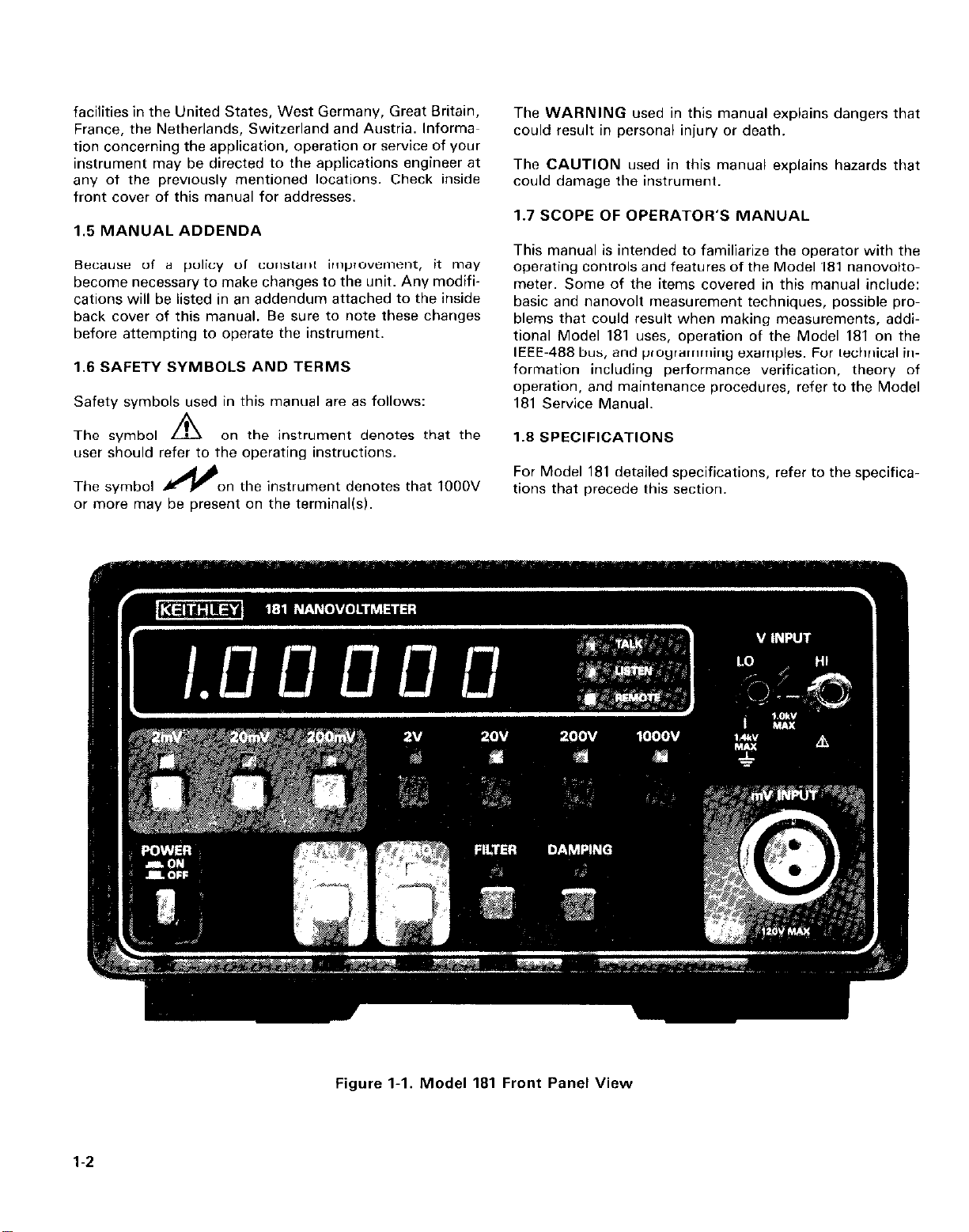
Model 181 Front Panel View. .............
Line Voltage Switch Location ............
Front Panel Controls and Connections
Rear Panel Controls and Connections.
Basic Voltage Measurements.
mV and nV Measurements ...............
Common Ground Connections for V and mV
Filter Response Graph. ..................
Analog Output Connections ..............
Xl000 Analog Output ...................
Source Resistance Consideration .........
Thermal emf Generation .................
Power Line Ground Loops ...............
Ground Loop Voltage Generation .........
Eliminating Ground Loops ...............
Standard Cell Comparison ...............
Absolute Cell Measurement Connections.
Low Resistance Measurement Connections.
Minimizing Josephson Junction RFI Effects
IEEE Bus Configuration ..................
IEEEHandshakeSequence ...............
Primary Address and IEEE Mode Switches.
IEEE Contact Configuration ..............
IEEE Bus Data Format ...................
Status Byte Format .....................
Programming Example ..................
Timing Diagram .......................
............
.....
.....
..
Title Page
......
......
......
......
......
......
......
......
......
......
......
......
......
......
......
......
......
......
......
.....
......
......
......
......
......
......
......
......
......
......
......
......
......
......
......
......
......
......
......
.....
......
......
......
......
......
......
......
......
......
......
......
......
......
......
......
......
......
......
......
......
......
......
......
.....
......
......
......
......
......
......
......
......
......
......
......
......
......
......
......
......
......
......
......
......
......
......
.....
..........
.......... 2-l
.......... 2-3
.......... 2-3
.......... 2-5
.......... 2-6
.......... 2-6
.......... 2-7
.......... 2-7
.......... 2-8
.......... 2-9
......... 2-10
..........
.......... 3-2
..........
.......... 4-l
.......... 4-2
..........
.......... 4-8
.......... 4-9
......... 4-11
l-2
2-4
2-4
2-9
3-l
3-2
3-3
4-3
4-3
4-13
Table
2-l
2-2
2-3
4-l
4-2
4-3
4-4
4-5
4-6
4-7
4-8
4-S
ii
Fuse Selection .........................
Settling Times .........................
Analog Output Parameters. ..............
IEEE Contact Designations ...............
Bus Command Summary ................
Device-Dependent Command Summary
Range Commands ......................
Default Conditions. .....................
Data String Exponent Values .............
Error and Data Code Summary ...........
Status Word Example ...................
HP-85 BASIC IEEE-488 Statements .......
LIST OF TABLES
...
......
......
......
......
......
......
......
......
......
., ....
Page
2-l
2-6
2-7
4-4
4-4
4-6
4-6
4-7
4-8
4-9
4-9
4-10
Page 5
SECTION 1
GENERAL INFORMATION
1.1 INTRODUCTION
The Keithley Model 181 is a highly sensitive nanovoltmeter
with a large, easy to read 5 K or 6 ‘/ digit display. The Model
181 is unique in that it combines microprocessor technology
with a new concept in low-noise, high-gain front ends,
resulting in a programmable instrument with sensitivity
down to 10nV. The Model 181 provides highly accurate,
stable, low-noise readings on seven ranges for DC voltage
measurements between 1OnV and 1OOOV. The mV ranges
use a special low-thermal input connector, while connections for the higher voltage ranges are made through two
S-way binding posts. Additional versatility is afforded by the
inclusion of an IEEE-488 interface which allows the unit to
communicate with other instrumentation.
1.2 MODEL 181 FEATURES
The Model 181 includes the following features:
l
High Sensitivity. The resolution of the Model 181 on the
2mV range is IO ~* volts (10nV).
l
5% or 6% Digit Resolution. Normal 5% digit display
resolution may be increased to 6 % digits at the touch of a
button.
l
IEEE-488 Interface. A built in IEEE-488 interface allows
the instrument to communicate with other devices such
as a central controller or printer.
l
Analog Output. An analog output, which accurately
reflects the displayed readings, is available from the rear
pallel.
l
3-p& Digital Filter. The internal 3-p& filter minimizes the
effects of noise in voltage readings and may be controlled
from the front panel or IEEE bus.
l
Separate Inputs. A special input connector is used for the
mV ranges to minimize thermal emf generation.
l
Isolated Low Terminals. The low signal connections for
both inputs are isolated from power line ground and
from IEEE low to minimize ground loop problems.
l
Color Coded Front Panel. Inputs, range switches, and
other front panel controls are marked to form color-coded
groups for easier operation.
1.3 OPTIONAL ACCESSORIES
1
Model 1483 Low-Thermal Connection Kit. The Model
1483 kit contains a crimp tool, pure copper lugs, Lowe
thermal cadmium solder, copper alligator clips, and
assorted hardware. It may be used for constructing experimental circuits with low-thermal connections to
minimize thermal emf effects.
2
Model 1484 Refill Kit. The Model 1484 kit contains
replacement parts for the Model 1483.
3
Model 1485 Low-Thermal Female Connector. The
Model 1485 connector is used for the mV INPUT on the
front panel of the Model 181.
4
Model 1486 Low-Thermal Male Connector. The Model
1486 connector mates with the Model 1485 female connector. It can be used to construct custom cables of
various lengths. This connector is used with the Model
1506 and 1507.
5
Model 1488 Low-Thermal Shorting Plug. The Model
1488 provides a means of shorting the mV INPUT to
check instrument offset and drift.
6
Model 1503 LawThermal Solder. The Model 1503 kit
contains low-thermal cadmium solder to make solder
connections for low voltage measurements.
7
Model 1506 Low-Thermal Input Cable. The Model 1506
cable is supplied with the unit It is a specially designed,
four foot triaxial cable that provides excellent shielding
for sensitive measurements. The Model 1506 has two
color coded alligator clips on one end, and a Model
1486 low-thermal male connector at the other end.
8
Model 1507 Low-Thermal Cable. The Model 1507 cable
is similar to the Model 1506. except that the alligator
clips are replaced by spade lugs. The Model 1507 is cons
strutted of a four foot triaxial cable and has a Model
1486 low-thermal male connector on one end.
9
Model 1815 Maintenance Kit. The Model 1815 kit cons
tains a calibration cover and extender cables that are
helpful when making service adjustments to the Model
181. The calibration cover replaces the top cover while
making these adjustments. The extender cables allow
individual PC cards to be partially removed from the unit
during maintenance.
10
Model 1019 Rack Mounting Kit. The Model 1019 kit
allows the Model 181 to be conveniently mounted in a
standard 19 inch rack.
A summary of the many optional Model 181 accessories is
listed in the following paragraphs. These accessories are
designed to enhance the capabilities of the instrument and
are described in more detail in the Model 181 Service
Manual, Document Number 30816. Contact the nearest
Keithley representative or the factory to obtain accessories.
1.4 WARRANTY INFORMATION
Warranty information may be found inside the front cover of
this manual. If warranty service is required, contact the
Keithley representative in your area or the factory to detw
mine the correct course of action. Keithlev maintains service
l-l
Page 6
facilities in the United States, West Germany, Great Britain,
France, the Netherlands, Switzerland and Austria. lnforma-
tion concerning the application, operation or service of your
instrument may be directed to the applications engineer at
any of the previously mentioned locations. Check inside
front cover of this manual for addresses.
1.5 MANUAL ADDENDA
Because of a policy of constant improvement, it may
become necessary to make changes to the unit. Any modifi-
cations will be listed in an addendum attached to the inside
back cover of this manual. Be sure to note these changes
before attempting to operate the instrument.
1.6 SAFETY SYMBOLS AND TERMS
Safety symbols used in this manual are as follows:
The WARNING used in this manual explains dangers that
could result in personal injury or death.
The CAUTION used in this manual explains hazards that
could damage the instrument.
1.7 SCOPE OF OPERATOR’S MANUAL
This manual is intended to familiarize the operator with the
operating controls and features of the Model 181 nanovolto-
meter. Some of the items covered in this manual include:
basic and nanovolt measurement techniques, possible problems that could result when making measurements, addi-
tional Model 181 uses, operation of the Model 181 on the
IEEE-488 bus, and programming examples. For technical information including performance verification, theory of
operation, and maintenance procedures, refer to the Model
181 Service Manual.
The symbol
A on the instrument denotes that the
user should refer to the operating instructions.
The symbol 1/2)
on the ,nstrument denotes that 1OOOV
or more may be present on the terminal(s).
1.8 SPECIFICATIONS
For Model 181 detailed specifications, refer to the specifications that precede this section.
1-2
Figure l-l. Model 181 Front Panel View
Page 7
SECTION 2
OPERATION
2.1 INTRODUCTION
This section contains information needed for basic Model
181 operation. Be sure to read this entire section before
attempting to operate the unit.
2.2 UNPACKING AND INSPECTION
The Model 181 was carefully inspected before shipment.
Upon receiving the unit, unpack all the items from the shipping carton and check for any damage that might have
occurred during shipment. Report any damage to the shipping agent at once. Save the original packing material for
possible future reshipment. Contact your nearest Keithley
representative or the factory if the unit fails to function
properly.
The following items are included with every Model 181
shipment:
1. Model 181 Nanovoltmeter
2. Model 181 Operator’s Manual
3. Model 181 Service Manual
4. Model 1506 Low-Thermal Input Cable
5. List of computer programs.
6. Additional accessories as ordered.
2.3 PREPARING FOR OPERATION
transformer must be installed. Contact your
Keithley representative or the factory for
information.
To remove the top cover. remove the two screws securing
the cover to the rear panel. Then lift off the cover from the
back until the tabs at the front of the cover clear the front
panel. Then remove the cover entirely.
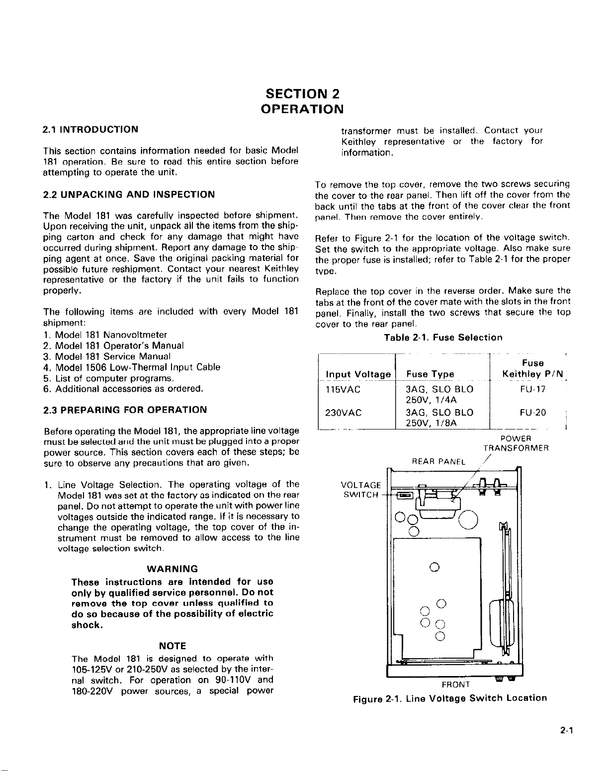
Refer to Figure 2-1 for the location of the voltage switch.
Set the switch to the appropriate voltage. Also make sure
the proper fuse is installed; refer to Table 2-l for the proper
type.
Replace the top cover in the reverse order. Make sure the
tabs at the front of the cover mate with the slots in the front
panel. Finally, install the two screws that secure the top
cover to the rear panel.
Table 2-1. Fuse Selection
3AG. SLO BLO
3AG. SLO BLO
Before operating the Model 181, the appropriate line voltage
must be selected and the unit must be plugged into a proper
power source. This section covers each of these steps; be
sure to observe any precautions that are given.
1. Line Voltage Selection. The operating voltage of the
Model 181 was set at the factory as indicated on the rear
panel. Do not attempt to operate the unit with power line
voltages outside the indicated range. If it is necessary to
change the operating voltage, the top cover of the instrument must be removed to allow access to the line
voltage selection switch.
WARNING
These instructions are intended for use
only by qualified service personnel. Do not
remme the top cover unless qualified to
do so because of the possibility of electric
shock.
NOTE
The Model 181 is designed to operate with
105.125V or 210.250V as selected by the inter-
nal switch. For operation on 90.IlOV and
180.22OV power sources, a special power
POWER
TRANSFORMER
REAR PANEL
/
/
FRONT
/-
WV=
VOLTAGE VOLTAGE
SWITCH SWITCH
Figure 2-l. Line Voltage Switch Location
Y
2-l
Page 8
2.
Power Line Connection. The Model 181 power cord is
supplied with a 3.prong plug that is designed to be used
with grounded outlets. Connect the female end of this
cord to the power receptacle on the rear panel of the
unit. Connect the other end to an appropriate power
SO”,lX.
CAUTION
Make sure the proper line voltage is
selected as described in the last section.
Failure to do so may result in damage to
the instrument,
possibly voiding the
warranty.
3.
Power-up Procedure. Once the power connections have
been made, the unit may be turned on by depressing the
front panel power switch. The Model 181 display should
show the line frequency and software revision level (e.g.
F60 b7) for approximately one second. After that, the
unit will revert to the normal display mode. In addition,
the 1OOOV range indicator light should be on. This is one
of the power-on default conditions that are explained
more fully in paragraph 4.5.
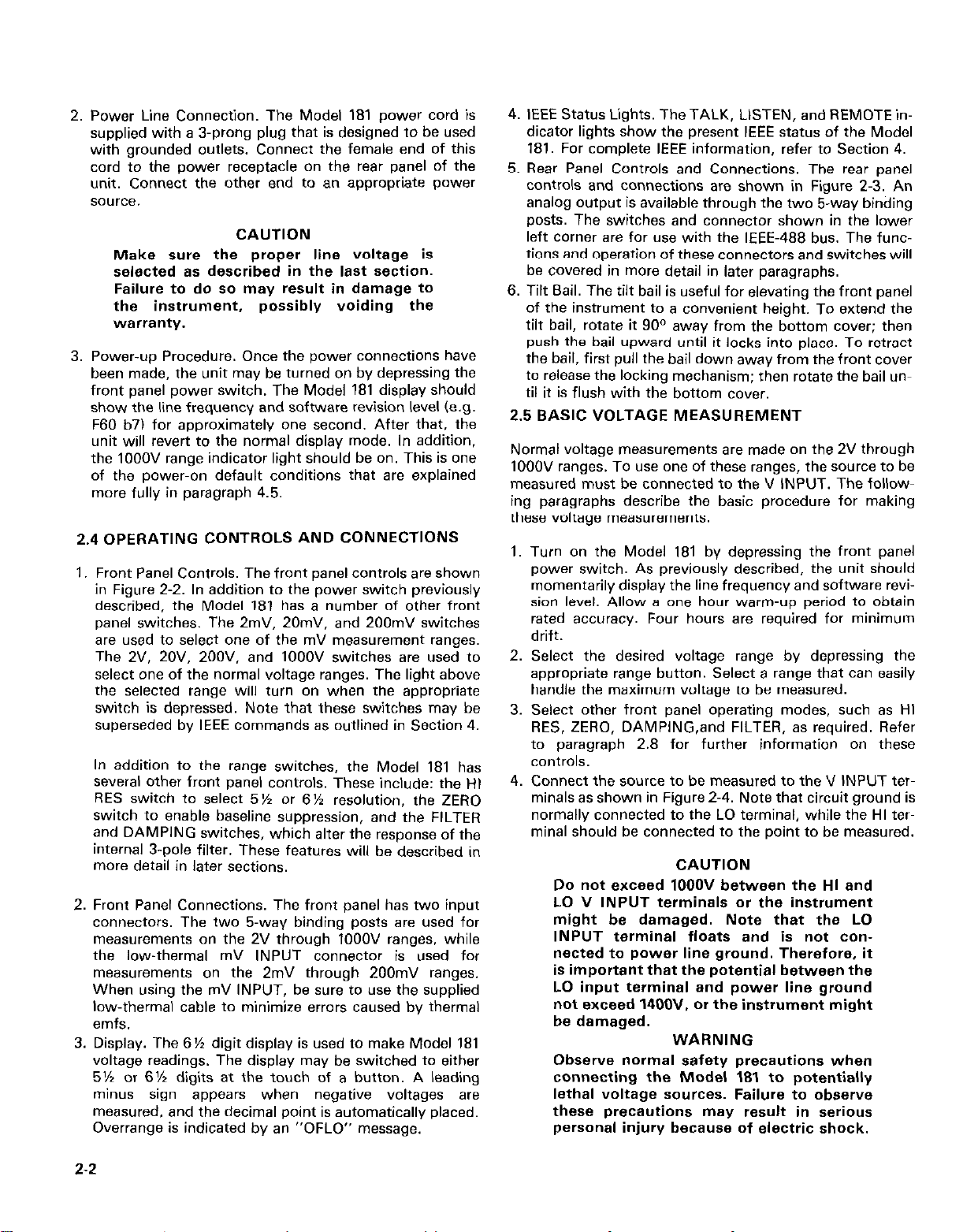
2.4 OPERATING CONTROLS AND CONNECTIONS
Front Panel Controls. The front panel controls are shown
in Figure 2-2. In addition to the power switch previously
described, the Model 181 has a number of other front
panel switches. The 2mV. 20mV. and 200mV switches
are used to select one of the mV measurement ranges.
The 2V. 2OV. 2OOV. and 1OOOV switches are used to
select one of the normal voltage ranges. The light above
the selected range will turn on when the appropriate
switch is depressed. Note that these switches may be
superseded by IEEE commands as outlined in Section 4.
In addition to the range switches, the Model 181 has
several other front panel controls. These include: the HI
RES switch to select 5% or 6% resolution, the ZERO
switch to enable baseline suppression, and the FILTER
and DAMPING switches, which alter the response of the
internal 3-pole filter. These features will be described in
more detail in later sections.
Front Panel Connections. The front panel has two input
connectors. The two 5.way binding posts are used for
measurements on the 2V through 1OOOV ranges, while
the low-thermal mV INPUT connector is used for
measurements on the 2mV through 200mV ranges.
When using the mV INPUT, be sure to use the supplied
low-thermal cable to minimize errors caused by thermal
emfs.
Display. The 6% digit display is used to make Model 181
voltage readings. The display may be switched to either
5% or 6% digits at the touch of a button. A leading
minus sign appears when negative voltages are
measured, and the decimal point is automatically placed.
Overrange is indicated by an “OFLO” message.
4. IEEE Status Lights. The TALK, LISTEN, and REMOTE indicator lights show the present IEEE status of the Model
181. For complete IEEE information, refer to Section 4.
5. Rear Panel Controls and Connections. The rear panel
Controls and connections are shown in Figure 2-3. An
analog output is available through the two 5-way binding
posts. The switches and connector shown in the lower
left corner are for use with the IEEE-488 bus. The functions and operation of these connectors and switches will
be covered in more detail in later paragraphs.
6. Tilt Sail. The tilt bail is useful for elevating the front panel
of the instrument to a convenient height. To extend the
tilt bail, rotate it 90’ away from the bottom cover; then
push the bail upward until it locks into place. To retract
the bail, first pull the bail down away from the front cover
to release the locking mechanism; then rotate the bail until it is flush with the bottom cover.
2.5 BASIC VOLTAGE MEASUREMENT
Normal voltage measurements are made on the 2V through
IOOOV ranges. To use one of these ranges, the source to be
measured must be connected to the V INPUT. The follow-
ing paragraphs describe the basic procedure for making
these voltage measurements.
Turn on the Model 181 by depressing the front panel
power switch. As previously described, the unit should
momentarily display the line frequency and software revision level. Allow a one hour warm-up period to obtain
rated accuracy. Four hours are required for minimum
drift.
Select the desired voltage range by depressing the
appropriate range button. Select a range that can easily
handle the maximum voltage to be measured.
Select other front panel operating modes, such as HI
RES, ZERO, DAMPING,and FILTER, as required. Refer
to paragraph 2.8 for further information on these
controls.
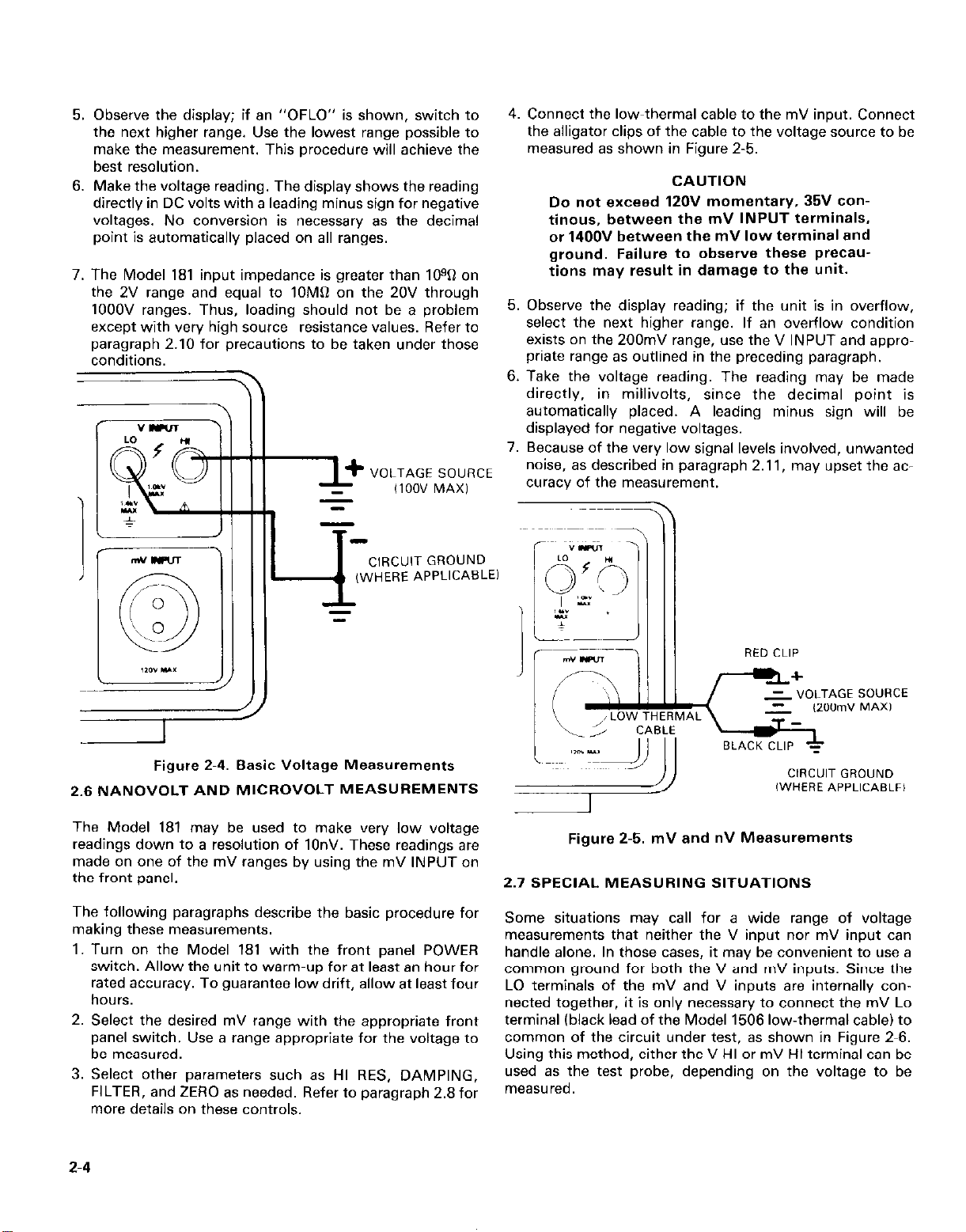
Connect the source to be measured to the V INPUT terminals es shown in Figure 2-4. Note that circuit ground is
normally connected to the LO terminal, while the HI terminal should be connected to the point to be measured.
CAUTION
Do not exceed IOOOV between the HI and
LO V INPUT terminals or the instrument
might be damaged. Note that the LO
INPUT terminal floats and is not connected to power line ground. Therefore, it
is important that the potential between the
LO input terminal and power line ground
not exceed 14OOV. or the instrument might
be damaged.
WARNING
Observe normal safety precautions when
connecting the Model 181 to potentially
lethal voltage sources. Failure to observe
these precautions may result in serious
personal injury because of electric shock.
2-2
Page 9
mV RANGES
DISPLAY
IEEE STATUS LIGHTS
- mV INPUT
ANALOG
OUTPUT
POWER
ON/OFF
0
II I
RESOLUTION
Figure 2-2. Front Panel Controls and Connections
^ ^ ^ .
U,SLUNNC
DISPLAY
* ,\
A?
ZERO
FILTER CONTROLS
V HANGES
ENABLE
AC RECEPTACLE
I ,Nt ClArlNG
.,,,,,. ,,, :r,. ,...
1
,. t.;,
,.,. ,,I_, . “,.L
ANALOG OUTPUT
RANGE SWITCH
IEEE CONNECTOR
Figure 2.3. Rear Panel Controls and Connections
2-3
Page 10
5. Observe the display; if an “OFLO” is shown, switch to
the next higher range. Use the lowest range possible to
make the measurement. This procedure will achieve the
best resolution.
6. Make the voltage reading. The display shows the reading
directly in DC volts with a leading minus sign for negative
voltages. No conversion is necessary as the decimal
point is automatically placed on all ranges.
7. The Model 181 input impedance is greater than 10% on
the 2V range and equal to lOMl7 on the 20V through
IOOOV ranges. Thus, loading should not be a problem
except with very high source resistance values. Refer to
paragraph 2.10 for precautions to be taken under those
conditions.
VOLTAGE SOURCE
,100” MAX,
7
-
CIRCUIT GROUND
,WHERE APPLICABLE1
-L
-
i
-I-
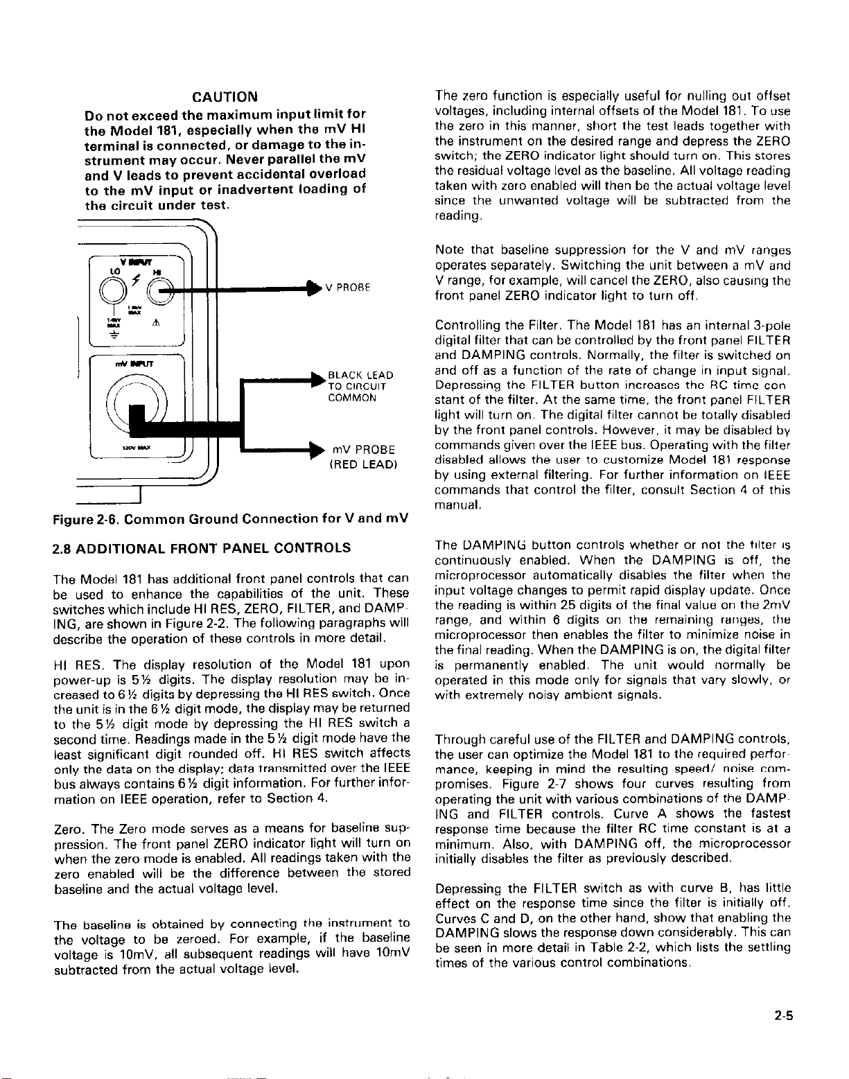
4. Connect the low-thermal cable to the mV input. Connect
the alligator clips of the cable to the voltage source to be
measured as shown in Figure 2-5.
CAUTION
Do not exceed 120V momentary. 35V con-
tinous, between the mV INPUT terminals.
or 1400V between the mV low terminal and
ground. Failure to observe these precau-
tions may result in damage to the unit.
5. Observe the display reading; if the unit is in overflow,
select the next higher range. If an overflow condition
exists on the 200mV range, use the V INPUT and appropriate range as outlined in the preceding paragraph.
6. Take the voltage reading. The reading may be made
directly, in millivolts,
automatically placed. A leading minus sign will be
displayed for negative voltages.
7. Because of the very low signal levels involved, unwanted
no,se, as CleSCrlDea I” paragrapn z.11, may upset the ac-
curacy of the measurement.
since the decimal point is
^
Figure 2-4. Basic Voltage Measurements
NANOVOLT AND MICROVOLT MEASUREMENTS
2.6
The Model 161 may be used to make very low voltage
readings down to a resolution of 10nV. These readings are
made on one of the mV ranges by using the mV INPUT on
the front panel.
The following paragraphs describe the basic procedure for
making these measurements.
1. Turn on the Model 181 with the front panel POWER
switch. Allow the unit to warm-up for at least an hour for
rated accuracy. To guarantee low drift, allow at least four
hours.
2. Select the desired mV range with the appropriate front
panel switch. Use a range appropriate for the voltage to
be measured.
3. Select other parameters such as HI RES, DAMPING,
FILTER, and ZERO as needed. Refer to paragraph 2.8 for
more details on these controls.
2-4
I
Figure 2-5. mV and nV Measurements
2.7 SPECIAL MEASURING SITUATIONS
Some situations may call for a wide range of voltage
measurements that neither the V input nor mV input can
handle alone. In those cases, it may be convenient to use a
common ground for both the V and mV inputs. Since the
LO terminals of the mV and V inputs are internally connected together, it is only necessary to connect the mV Lo
terminal (black lead of the Model 1506 low-thermal cable) to
common of the circuit under test, as shown in Figure 2-6.
Using this method, either the V HI or mV HI terminal can be
used as the test probe, depending on the voltage to be
measured.
Page 11
CAUTION
Do not exceed the maximum input limit for
the Model 181, especially when the mV HI
terminal is connected. or damage to the in-
strument may occur. Never parallel the mV
and V leads to prevent accidental overload
to the mV input or inadvertent loading of
the circuit under test.
Figure 2-6. Common Ground Connection for V and mV
The zero function is especially useful for nulling out offset
voltages, including internal offsets of the Model 181. To use
the zero in this manner, short the test leads together with
the instrument on the desired range and depress the ZERO
switch; the ZERO indicator light should turn on. This stores
the residual voltage level as the baseline. All voltage reading
taken with zero enabled will then be the actual voltage level
since the unwanted voltage will be subtracted from the
reading.
Note that baseline suppression for the V and mV ranges
operates separately. Switching the unit between a mV and
V range, for example, will cancel the ZERO, also causing the
front panel ZERO indicator light to turn off.
Controlling the Filter. The Model 181 has an internal 3-p&
digital filter that can be controlled by the front panel FILTER
and DAMPING controls. Normally, the filter is switched on
and off as a function of the rate of change in input signal.
Depressing the FILTER button increases the RC time conk
stant of the filter. At the same time, the front panel FILTER
light will turn on. The digital filter cannot be totally disabled
by the front panel controls. However, it may be disabled by
commands given over the IEEE bus. Operating with the filter
disabled allows the user to customize Model 161 response
by using external filtering. For further information on IEEE
commands that control the filter, consult Section 4 of this
manual.
2.8 ADDITIONAL FRONT PANEL CONTROLS
The Model 181 has additional front panel controls that can
be used to enhance the capabilities of the unit. These
switches which include HI RES, ZERO, FILTER, and DAMP-
ING, are shown in Figure 2-2. The following paragraphs will
describe the operation of these controls in more detail.
HI RES. The display resolution of the Model 181 upon
power-up is 5% digits. The display resolution may be increased to 6 % digits by depressing the HI RES switch. Once
the unit is in the 6% digit mode, the display may be returned
to the 5% digit mode by depressing the HI RES switch a
second time. Readings made in the 5% digit mode have the
least significant digit rounded off. HI RES switch affects
only the data on the display; data transmitted over the IEEE
bus always contains 6% digit information. For further infor-
mation on IEEE operation, refer to Section 4.
Zero. The Zero mode serves as a means for baseline sup-
pression. The front panel ZERO indicator light will turn on
when the zero mode is enabled. All readings taken with the
zero enabled will be the difference between the stored
baseline and the actual voltage level.
The baseline is obtained by connecting the instrument to
the voltage to be zeroed. For example, if the baseline
voltage is IOmV, all subsequent readings will have 1OmV
subtracted from the actual voltage level.
The DAMPING button controls whether or not the filter is
continuously enabled. When the DAMPING is off, the
microprocessor automatically disables the filter when the
input voltage changes to permit rapid display update. Once
the reading is within 25 digits of the final value on the 2mV
range, and within 6 digits on the remaining ranges. the
microprocessor then enables the filter to minimize noise in
the final reading. When the DAMPING is on. the digital filter
is permanently enabled. The unit would normally be
operated in this mode only for signals that vary slowlv, or
with extremely noisy ambient signals.
Through careful use of the FILTER and DAMPING controls,
the user can optimize the Model 161 to the required perfw
mance, keeping in mind the resulting speed/ noise compromises. Figure 2-7 shows four curves resulting from
operating the unit with various combinations of the DAMPS
ING and FILTER controls. Curve A shows the fastest
response time because the filter RC time constant is at a
minimum. Also, with DAMPING off, the microprocessor
initially disables the filter as previously described.
Depressing the FILTER switch as with curve 6, has little
effect on the response time since the filter is initially off.
Curves C and D, on the other hand, show that enabling the
DAMPING slows the response down considerably. This can
be seen in more detail in Table 2-2, which lists the settling
times of the various control combinations.
2-5
Page 12
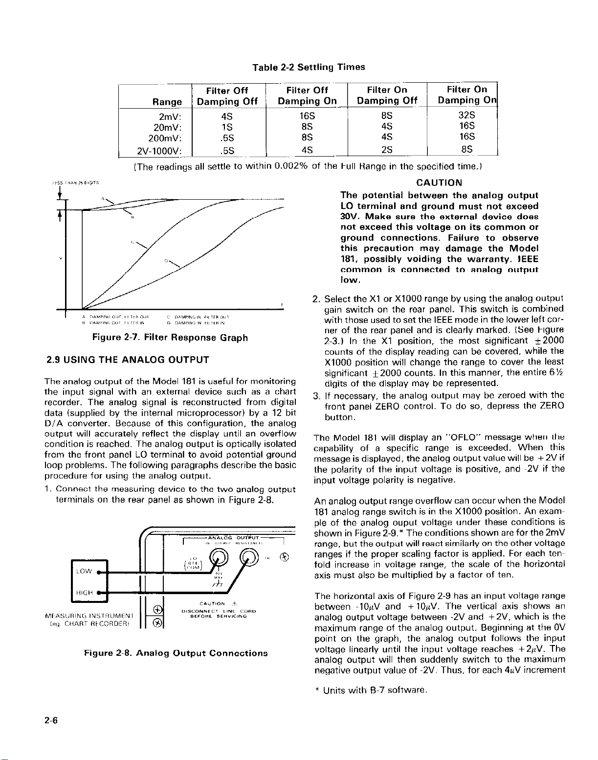
Table 2-2 Settling Times
~~~~~-~~~~“~~~~~
(The readings all settle to within 0.002% of the Full Range in the specified time.)
2.9 USING THE ANALOG OUTPUT
The analog output of the Model 181 is useful for monitoring
the input signal with an external device such as a chart
recorder. The analog signal is reconstructed from digital
data (supplied by the internal microprocessor) by a 12 bit
D/A converter. Because of this configuration, the analog
output will accurately reflect the display until an overflow
condition is reached. The analog output is optically isolated
from the front panel LO terminal to avoid potential ground
loop problems. The following paragraphs describe the basic
procedure for using the analog output.
1. Connect the measuring device to the two analog output
terminals on the rear panel as shown in Figure 2-8.
CAUTION
The potential between the analog output
LO terminal and ground must not exceed
30V. Make sure the external device does
not exceed this voltage on its common or
ground connections. Failure to observe
this precaution may damage the Model
181. possibly voiding the warranty. IEEE
common is connected to analog output
IOW.
Select the Xl or Xl000 range by using the analog output
gain switch on the rear panel. This switch is combined
with those used to set the IEEE mode in the lower left cor-
ner of the rear panel and is clearly marked. (See Figure
2.3.) In the Xl position, the most significant +2000
counts of the display reading can be covered, while the
Xl000 position will change the range to cover the least
significant f2000 counts. In this manner, the entire 6%
digits of the display may be represented.
If necessary, the analog output may be zeroed with the
front panel ZERO control. To do so, depress the ZERO
button.
The Model 181 will display an “OFLO” message when the
capability of a specific range is exceeded. When this
message is displayed. the analog output value will be + 2V if
the polarity of the input voltage is positive, and -2V if the
input voltage polarity is negative.
An analog output range overflow can occur when the Model
181 analog range switch is in the Xl000 position. An example of the analog ouput voltage under these conditions is
shown in Figure 2-9.” The conditions shown are for the 2mV
range. but the output will react similarly on the other voltage
ranges if the proper scaling factor is applied. For each ten-
fold increase in voltage range, the scale of the horizontal
axis must also be multiplied by a factor of ten.
2-6
Figure 2-8. Analog Output Connections
The horizontal axis of Figure 2-9 has an input voltage range
between -10&V and +lOpV. The vertical axis shows an
analog output voltage between -2V and +ZV. which is the
maximum range of the analog output. Beginning at the OV
point on the graph, the analog output follows the input
voltage linearly until the input voltage reaches +2pV. The
analog output will then suddenly switch to the maximum
negative output value of -2V. Thus, for each 4uV increment
* Units with B-7 software.
Page 13
in input voltage, the output pattern repeats. ihe action of
the analog output for negative input voltages is the same,
except that the slope of the graph is negative for these
negative-going input voltages.
Figure 2-9. Xl000 Analog Output
By counting the number of repeating waveforms on a chart
recorder, the user can easily determine the actual voltage at
the input, even though the range of the analog output was
exceeded. If, for example, the +lV point on the second
peak with a positive-going slope is noted, it can be clearly
determined that the input voltage was +5@V at that particular time.
A summary of analog output information is shown in Table
2.3. Each range of input values corresponds to the incre-
ment necessary to cause the output to go through its entire
0 to 2V range. Note that the sensitivity is increased by a fac-
tor of a thousand on the Xl000 range. For example, when
the Model 181 is in the 200mV range, and the analog switch
is in the Xl position, the output voltage will swing from 0 to
2V in a smooth manner as the input voltage increases
gradually from 0 to 200mV. When the analog output switch
is changed to the Xl000 position, the input need only swing
between 0 and 2OOpV to obtain the same voltage swing at
the analog output. Beyond those input limitations, the out-
put voltage will repeat as shown in Figure 2-9.
The output resistance of the analog ouput is Ikll for all
voltage ranges regardless of the position of the analog range
switch. Thus, loading problems caused by external devices
are minimized. To keep loading errors below I%, the input
resistance of any device connected to the analog output
should be greater than lOOk0.
Table 2-3. Analog Output Parameters
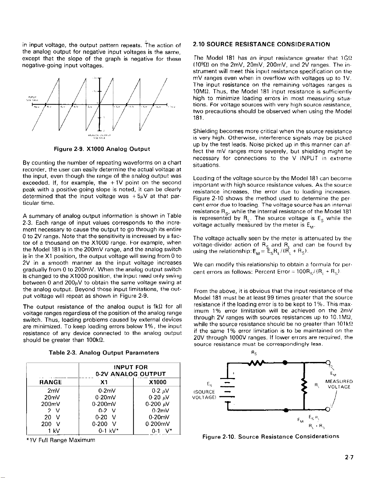
2.10 SOURCE RESISTANCE CONSIDERATION
The Model 181 has an input resistance greater that IGIl
flO% on the 2mV. 20mV. 200mV. and 2V ranges. The in-
strument will meet this input resistance specification on the
mV ranges even when in overflow with voltages up to 1V.
The input resistance on the remaining voltages ranges is
lOML2. Thus, the Model 181 input resistance is sufficiently
high to minimize loading errors in most measuring situations. For voltage sources with very high source resistance,
two precautions should be observed when using the Model
181.
Shielding becomes more critical when the source resistance
is very high. Otherwise, interference signals may be picked
up by the test leads. Noise picked up in this manner can affect the mV ranges more severely. but shielding might be
necessary for connections to the V INPUT in extreme
situations.
Loading of the voltage source by the Model 181 can become
important with high source resistance values. As the source
resistance increases, the error due to loading increases.
Figure Z-10 shows the method used to determine the Peru
cent error due to loading. The voltage source has an internal
resistance R,, while the internal resistance of the Model 181
is represented by R,. The source voltage is E, while the
voltage actually measured by the meter is E,.
The voltage actually seen by the meter is attenuated by the
voltage-divider action of R and R, and can be found by
using the relationship: E, = &R,IIRL + I?,).
We can modify this relationship to obtain a formula for per-
cent errors as follows: Percent Error = lOOR,/(R, * R,i~
From the above, it is obvious that the input resistance of the
Model 181 must be at least 99 times greater that the source
resistance if the loading error is to be kept to 1%. This maximum 1% error limitation will be achieved on the 2mV
through 2V ranges with sources resistances up to lO.lMI1,
while the source resistance should be no greater than IOlklI
if the same 1% error limitation is to be maintained on the
2OV through IOOOV ranges. If lower errors are required, the
source resistance must be correspondingly less.
Rs
20mV
200mV
2v
20 v
200 v
1 kV
*IV Full Range Maximum
INPUT FOR
IG OUTPUT
Figure 2-10. Source Resistance Considerations
2-7
Page 14

2.11 MICROVOLT AND NANOVOLT MEASUREMENT
CONSIDERATIONS
Low level voltage measurements are subject to various
types of noise that can make it difficult to obtain accurate
voltage readings. Since the measuring instrument cannot
distinguish between signal and noise voltages, the presence
of unwanted low level signals can seriously affect a
measurement. Some of the phenomena that can cause unwanted noise include: thermocouples (thermoelectric
effects), flexing of coaxial cables (triboelectric effects), and
the battery action of two terminals (galvanic action). The
following paragraphs will discuss potential noise sources in
more detail.
Source Resistance Noise, Noise that is present in the source
resistance itself is frequently the determining factor in the
ultimate resolution of a measurement system. The amount
of noise in a given resistance is given by the Johnson Noise
‘wE”= ~+:;;Js:
Noise Bandwidth in Hertz
. L’
IL
At a room temperature of 293’=K (20°C). the above can be
simplified to read: E.,,= 1.27~ IO- lm
It has been statistically shown, that p-p n&e is aPProximately five times the rms noise 99% of the time. From this
relationship, we
E
=6.35~1O-‘~F
0~”
From the preceding equations it is immediately obvious
that the noise voltage can be reduced by lowering the
temperature, reducing the resistance, or narrowing the
bandwidth. Reducing the resistance is not very useful
because the signal voltage will be reduced more than the
noise. For example, decreasing the resistance of a current
shunt by a factor of 100 will reduce the signal voltage by a
factor of 100 as well; the noise, however, will be reduced
only by a factor of 10.
Very often, cooling is the only practical method available to
reduce the noise. Here again, the reduction available is not
as large as it seems because the noise reduction is related to
the square root of the change in temperature. For example,
to cut the noise voltage in half, the temperature must be
decreased from ‘293°K to 73.25OK. a fourfold decrease.
Source Resistance in Ohms
Temperature OK
Boltrman’s Constant Il.38 x 10-23)
can
equate
the following:
Thermoelectric potentials. Thermal emf’s are small electric
potentials generated by differences in the temperature at
the junction of two dissimilar metals.
Thermal emf’s are particularly troublesome at the low signal
levels measured by the mV ranges. To minimize thermal emf
drift, use copper leads to connect the circuit to the instrument. The Model 1506 low-thermal cable supplied with the
Model 181 is ideal for this purpose. Other suitable lowthermal items are listed in paragraph 1.3 Optional
Accessories.
Even with low-thermal cables and connectors, thermal
emf’s can still be a problem in some cases. It is especially
important to keep the two materials forming the junctions at
the same temperature. Keeping the two junctions close
together is one way to minimize such thermal problems. In
some cases, connecting the two junctions together with
good thermal contact to a common heat sink may be
required.
Most good electrical insulators have good thermal insulation
characteristics as well. In cases where such low-thermal
conductivity may be a problem, special insulators that combine high electrical insulating properties with high thermal
conductivity may be used. Some examples of materials with
low electrical conductivity and high thermal conductivity
are: hard anodized aluminum, beryllium oxide, specially
filled epoxy resin, sapphire, and diamond.
Oxidation of leads and connectors can also lead to thermal
emf problems. When copper oxidizes, for example, the
resulting copper to copper oxide junction can cause thermal
emf’s as high as lOOOpV/OC. Thus, it is imperative that all
connections be kept as clean as possible.
Figure 2-l 1 shows a representation of how thermal emf’s
between two dissimilar metals are generated. The test leads
are made of the A material, while the B material is ~the
source under test. The temperatures between the junctions
are represented by T, and T,. To find the thermal emf for the
circuit, the following relationship pay be used:
E, = Q,,(T, T>,
-Temperature of the A to B
junction in OC or OK.
Temperature of the B to A
junction in OC or OK.
Thermoelectric coefficient of material A
with respect to B, given in aVI°C.
As an example of determining noise voltage generation,
assume that the Model 181 is connected to a voltage source
with an internal resistance of lOk!l. At a room temperature
of 20°C (293’K). the p-p noise voltage generated cwer a
bandwidth of 0.5Hz will be:
E
=6.35x 10~~‘“jUOx 103)(0.5)
P’P
E,~,=4.5x lo-*V=45nV
2-6
1
Figure Z-11. Thermal EMF Generation
I
Page 15

In the unlikely avant the two junction temperatures are identical, the thermal emf’s will exactly cancel, since the
generated potentials oppose one another. More often, the
two junctions temperatures will differ, and considerable
thermal emf’s will be generated.
A typical test set up might have one or more copper to
cadmium-tin junctions. Typically. such a junction has a thermoelectric coefficient of O.~FV/~C. Since the two materials
will frequently have a several-degree temperature differential, it is easy to see how thermal potentials of several
microvolts can be generated, even if reasonable precautions
are taken.
Magnetic fields. When a conductor cuts through magnetic
lines of force, a very small currant is generated. This
phenomenon will frequently cause unwanted signals to
occur in the test leads of a measuring instrument. If the conductor has sufficient length, even weak magnetic fields
such as the earth’s can create sufficient signals to upset
voltage measurements in the nanovolt or millivolt ranges.
Thus, several precautions may be taken if magnetic-field in-
duced signals become a problem.
Reducing the length of the leads or minimizing the exposed
circuit area are two ways these effects can be minimized. In
extreme cases, magnetic shielding may be required. Special
metals with high permeability at low flux densities (such as
mu metal) are effective in this application.
Figure Z-12. Power Line Ground Loops
To see how a ground loop can affect the voltage readings,
refer to Figure Z-13. The source to be measured is connected to the nanovoltmeter through the customary HI and
LO leads. The resistance of the LO terminal connection is
represented by R,. This resistance is usually very low
about 0.111, but even this low value can be significant if the
circulating current is high enough.
Even in cases where the conductor is stationary,
magnetically induced signals may be a problem. Fields may
be produced by various signals such as the AC power line
voltage. Large inductors such as power transformers are
very good magnetic field generators, so care must be taken
to keep the measuring circuit a good distance away from
these potential noise sources.
At high current levels, even a single conductor can generate
significant fields. These effects can be minimized by using
twisted pairs; using this method, the resulting fields will be
largely cancelled out.
Ground Loops. When two or more devices are connected
together, care must be taken to avoid unwanted signals
caused by ground loops. Ground loops usually occur when
sensitive instrumentation, such as the Modal 181. is con-
nected to other instrumentation with more than ona Signal
return path. One of these return paths may be power lina
ground. The resulting ground loop causes CUrrant t0 flow
through the instrument LO signal leads and than back
through the power line ground (See Figure Z-12). Bacausa
of this circulating currant, a small but undesireable voltage
is developed between the LO terminals of the two instruments. This voltage will be added to the swrca voltage.
upsetting the measurement.
GROUND
Figure Z-13. Ground Loop Voltage Generation
The source voltage is Es, while the ground loop currant is I,.
The actual voltage seen by the nanovoltmeter is the sum of
the source voltage and the IR drop across the LO lead connections, and can be found by using the relationship:
E,,=Es+I,R,
Thus, for a IOOnV source voltage, an R, value of 0.111, and a
IOOnA ground loop currant, the total voltage actually seen
by the instrument will be 1lOnV. creating an error of 10%.
Figure Z-14 shows a configuration that will eliminate this
type of ground loop problem. Here, only the center instrument is connected to ground. Ground loops are not normally a problem with the Model 181 because the LO input
terminals are isolated from power line ground. However, the
mV INPUT and V INPUT LO terminals should not be externally connected together as this will create a ground loop.
Also, since other instruments may not be designed in the
same way, they may cause ground loop problems even
though the Model 181 is isolated. When in doubt, consult
the manual for other instrumentation in the test setup.
2-9
Page 16

ments. With either type of RFI, the affect on instrument performance can be considerable if enough of the unwanted
signal is present.
P”WGR LINC mO”No
I
Figure 2-14. Eliminating Ground Loops
~RFI. Radio Frequency Interference (RF11 is a general term to
describe electromagnetic interference over a wide range of
frequencies across the spectrum. RFI can be especially
troublesome at the low signal levels measured on the mV
ranges, but it may also affect readings on the higher voltage
ranges in extreme cases.
RFI can be caused by steady-state sources such as TV or
radio broadcast signals, or it can result from impulse
sources, as in the case of arcing in high voltage environ-
RFI can be minimized by taking one or more of several
precautions when operating the Model 181 in such environ-
ments. The most obvious method for minimizing these
effects is to keep the instrument as far as possible away
from the source. Shielding the instrument, voltage source,
and test leads will often reduce RFI to an acceptable level. In
extreme cases, a specially constructed screen room may be
required to sufficiently attenuate the troublesome signal.
The internal 3-p& filter within the Model 181 may help
reduce RFI in home situations. For more serious RFI pro-
blems, the user is encouraged to try more effective external
shielding.
2-10
Page 17

SECTION 3
APPLICATIONS
3.1 INTRODUCTION
The high sensitivity and very high input impedance of the
Model 181 makes it ideal for critical measurements ordinary
DVM’s are unable to handle. Some of these applications, including standard cell comparison and low resistance
measurements, are covered in the following paragraphs.
3.2 STANDARD CELL COMPARISONS
The Model 181 may be used for making standard cell com-
parisons without the usual problems caused by different
ground connections. The input low terminals on the instru-
ment are isolated from ground, eliminating the possibility of
shorting out one of the cells when the input connections are
reversed.
The greatest concern when making such comparisons is the
effect of the measuring instrument on the standard cell
voltage. The Model 181 input characteristics minimize these
effects because of high input impedance and very low offset
current.
The equivalent circuit for making standard cell comparisons
is shown in Figure 3-l. V, and V, represent the two standard
cells being compared, and are connected to the HI and LO
mV INPUT terminals as shown. The common terminals of
the two cells are normally connected to earth ground to pre-
vent electrostatic pickup. Because of the high impedance
nature of the measurement, it may be necessary to shield
the two standard ceils. This shield should also be connected
to earth ground as shown in Figure 3-l.
The amount of current and charge drawn from the cells in
Figure 3-1 is determined by the common-mode and normalmode impedances. The common-mode impedance appears
only across V, and is represented by the parallel comblna-
tion of R,, (> 109% and Cc, (O.O015,,F.) Under typical
laboratory conditions lless than 60% relative humidity). the
value of R,,
ally be assumed to be infinite. The capacitance of the Model
1506 low-thermal cable makes up the larger portion of C,,.
If the input capacitance should have a detrimental effect on
standard cell performance, its value may be essentially
balanced out by connecting a 15OOpF capacitor between
the input HI terminal and earth ground. Since C,, will rarely
affect cell performance, this balancing technique is not
usually necessary.
The normal-mode impedance is represented by the parallel
combination of R,, and C,,. This normal-mode impedance
appears between the LO and HI input terminals. The actual
amount of charge and current drawn from the two cells
depends on the voltage difference between them (V,~V,I.
Typically, the potential difference between V, and V, is 1mV
or less, resulting in a charge of approximately 10 l2
coulombs that must be supplied by the two cells. In addi~
tion. an input offset current of less than 50pA is drawn from
the cells under test. Any effects from internal spikes pm
duced by the input multiplexing FET’s will be at a minimum,
as the spikes will occur at the 4Hr multiplexing rate.
When on the mV ranges. the Model 181 will maintain its
high input resistance characteristics ( ) 10%) for all voltages
up to lV, even during range changes or when in overload.
However, the input impedance drops substantially if the 1V
limitation is exceeded. To avoid possible cell degredation
under such conditions, it is recommended that a series
resistance 1 MR or greater be connected in series with one of
the cells, as shown in Figure 3-l. where R, is connected be-
tween V, and the input HI terminal. This safeguard will also
protect the cells from degradation in case of improper con-
nections. This resistance. Rs. can be shorted Out after an on
scale indication is observed, and the reading can then be
made in the normal manner.
is in the lo”12 to 1O’21l range. and may genw
Figure 3-I. Standard Cell Comparison
With this connection, it is assumed that the Model 181 is
connected to the power line with the standard 3.prong plug.
Since the power line ground is also connected to earth
ground, the complete ground connections will be made
through the ground wire in the line cord of the instrument.
The basic procedure for making standard cell measurements
involves connecting the two cells for comparison to the mV
INPUT and sening up the Model 181 as follows:
1. Turn on the power to the Model 181 and allow a one hour
warm-up period for the best accuracy. A four hour period
is required to minimize drift.
2. Connect the cells to the Model 181 as shown in Figure
3-1, Use the low-thermal cable and mV INPUT on the ins
strument. Include a lMI2 resistor for R, if the cells ate to
be protected from accidental loading during set-up.
3-l
Page 18

3. Select the appropriate mV range and observe the reading.
If the display reading jumps around excessively, enable
the damping with the front panel DAMPING switch.
4. Observe the readings; once the display has stabilized,
short R, (if connected), and take the voltage readings.
5. Remove the short from R, and reverse the lead connec-
tions to V, and V,. The LO terminal should now be con-
nected to V, and the HI terminal should be connected to
V,. Disable the damping to reduce settling time. Once the
reading has stabilized, enable the damping again, if
necessary. Once again, short R, and record the display
reading.
6. The standard cell difference may be found by averaging
the absolute values of the two readings as follows:
Cell Difference = (Reading In Step 41 + 1 Reading In Step 51
2
This averaging method is necessary to cancel thermal
effects, but either reading alone may be sufficiently accurate if precautions to minimize thermal emf generation are
observed. The ZERO button may be used to null any
residual offset. Also, only copper to copper connections
should be used to minimize such thermal effects. As always,
the connections should be kept as clean as possible, or the
resulting copper to copper oxide junctions may create substantial thermal emf voltage, upsetting the measurement.
range for input voltages above 200mV; the input impedance
on the mV ranges drops to IkR for inputs greater than IV.
Figure 3-Z. Absolute Cell Measurement Connections
3.3 LOW RESISTANCE “LINDECK” MEASUREMENTS
As with the standard cell comparisons, the high resolution
of the Model 181 gives the instrument a definite advantage
in speed and convenience over potentiometer systems traditionally used to make low resistance measurements.
The method just described is useful for comparing two standard cell voltages. However, some situations may call for
the measurement of a single cell alone. For measuring
absolute standard cell voltages, it is best to use the2V range
because the input impedance is greater than IOQ.
NOTE
Since the input impedance on the ZOV-1OOOV
ranges drops to lOM12, those voltage ranges are
unsuitable for making absolute standard cell
voltage measurements.
Figure 3-2 shows the connections for making absolute standard cell voltage measurements. Once again, R, is to be left
in the circuit until the reading is actually taken. The basic
procedure for making the absolute voltage measurement is
as follows:
1. Turn on the instrument and allow a one hour warm-up
period. Four hours are required to minimize drift,
2. Connect the standard cell to the instrument as shown in
Figure 3-2. Be sure to include R, to protect the cell,
3. Switch the instrument to the 2V range and observe the
reading. Be sure the reading is on range.
4. Short out R, and take voltage reading. Once the reading
is complete, remove the short from R,.
The method used with the Model 181 places a current
source in parallel with the low resistance to be measured, as
shown in Figure 3-3. The problem with such measurements
has generally been the trade-off between the power level required and the sensitivity of the instrument. In a circuit with
a .Olfl resistance, a current source delivering only IOmA will
provide a resolution of 0.01% with the Model 181 on the
2mV range. In contrast, a 1pV resolution DVM would require a current of IA. With the Model 181 measurement, the
power level in the resistor will be only 1pW. whereas the
measurement made with the DVM would result in a power
level of IOmW in a .OlR resistance.
With this method, the resistance may be found simply by
dividing the voltage reading by the current source value.
With a 1OmA current source and ,010 resistance, for exam-
ple, a voltage of IOOpV will be developed across the
measured resistance.
MODEL 181
Care should be taken when making absolute readings in this
way. If higher voltage ranges are used, the lower input im-
pedance will degrade cell performance. Do not use the mV
3-2
Figure 3-3. Low Resistance Measurement Connections
Page 19

3.4 TEMPERATURE MEASUREMENTS
The Model 181 may be used with thermocouples or ther-
mopiles to monitor small temperature changes down to a
resolution of ~O.OOl°C. Connections should be made using
appropriate low-thermal materials such as those supplied
with the Model 1483 Low-Thermal Connection Kit.
Although some shielding is recommended, the high AC re-
jection of the instrument eliminates most of the problems
normally caused nearby AC operated equipment such as
heaters, fans, pumps, etc.
The rear panel analog output may be used along with a
chart recorder to provide a continuous, permanent record of
temperature changes. Alternately, the Model 181 may be
connected to the IEEE-488 bus to allow easy transfer of
temperature data to a printer or computer. With a suitable
controller, the user may take full advantage of Model 181
capabilities, providing full automation of such temperature
tests.
appropriate controller and other instrumentation, virtually
complete automation of the necessary instrumentation
curve measurements may be obtained.
Josephson Junction measurements are especially vulnw
able to the effects of high frequency EMI (Electromagnetic
Interference) and RFI (Radio Frequency InterferenceI. Much
of this interference may be generated by the microprocessor
based instrumentation itself. Still other forms of interference may come from the outside environment. In either
case, care must be taken to minimize the coupling of these
unwanted signals to the device under test. The almost 1”~
evitable high-frequency coupling of unwanted RFI to the
Josephson Junction itself will significantly affect the I-V
characteristics of the device, rendering the data useless in
many cases. The Model 181 has been carefully designed to
minimize common-mode RFI that may be coupled through
the input cable to the device under test. However. depend
ding on the measuring environment, additional precautions
may be required.
3.5 RESISTANCE THERMOMETRY
The Model 181 may be used for resistance thermometry
where small deviations are measured with nW power dissipation levels. A stable current source may be used to provide the necessary constant low-level current. A typical
resolution, using a IOOOfl germanium thermometer (at
4.2”K) is O.OOOZ°C, with a power dissipation of only 1nW.
(lo-SW).
The floating input of the Model 181 eliminates the problems
usually encountered when floating four-terminal measurements are made. Note that the Model 181 may be used with
a wide range of source resistances, because of the high
input impedance of the unit. As with other Model 181 applications, thermometry measurements may be controlled
over the IEEE-488 bus.
3.6 SEMICONDUCTOR TESTING
The Model 181 may be used for semiconductor testing on
an automated production-line basis. Sensitive measure-
ments can be made on semiconductor devices to determine
gain stability, temperature coefficient, etc., without the
loading errors associated with many types of equipment. By
applying proper programming techniques, a high level of
automation through use of the IEEE-488 bus can be
achieved.
Two methods of minimizing RFI effects are shown in Figure
3-4. The device under test is placed within a shielded booth,
which is connected to earth ground. Also, a ferrite inductor
is placed in series with the HI input lead of the lowthermal
cable. This inductor is made up of 4 turns of #28 wire wound
around a Keithley CT-7 ferrite core (Fai-rite #2643000701 I.
Note that the inductor is placed just outside the shield, right
at the point where the input cable enters the shielded area.
These precautions should eliminate all but the most stubborn RFI problems. In more extreme situations. a second
inductor, identical to the first, may be connected in series
with the LO input in a similar manner.
3.7 JOSEPHSON JUNCTION STUDIES
The Model 181 can be used for Josephson Junction studies,
where speed and high sensitivity are a primary requirement.
Josephson Junction I-V characteristics can be easily plotted
using the Model 181 in conjunction with other instrumenta-
tion connected to the IEEE-488 bus. Through the use of an
Figure 3-4. Minimizing Josephson Junction RFI Effects
3-313-4
Page 20

Page 21

SECTION 4
IEEE OPERATION
4.1 INTRODUCTION TO THE IEEE-488 BUS
The Model 181 has a built in IEEE-488 bus that allows the
user to give commands and read data via an external device.
All the front panel operating modes except power on-off
may be controlled by commands given over the bus.
The Model 181 may be commanded over the bus when the
rear panel TO/ADDRESSABLE switch is in the
ADDRESSABLE position. When in the TO (talk only) mode,
the Model 181 merely outputs data on the bus: no com-
mands may be given when the unit is in this mode. For fur-
ther information on changing the mode of operation, see
paragraph 4.3
A typical bus set-up for controlled operation is shown in
Figure 4-l. A typical system will have one controller and
several other instruments to which commands are given.
Generally, there are three catagories that describe device
operation. These catagories are: controller: talker; listener.
The controller does what its name implies: it controls the
other instruments on the bus. A talker sends data, while a
listener receives data. Depending on the type of instrument,
any particular device may be a talker only, a listener only. or
both a talker and a listener. The Model 181 is capable of
being both a talker and a listener, but does not have the
capability of being a controller.
Any given system can have only one controller, but any
number of talkers or listeners may be present up to the hardware constraints of the bus (see paragraph 4.2). Several
devices may be commanded to listen at once, but only one
talker can be active at any given time.
Before a device can talk or listen, it must be appropriately
addressed. Devices are selected on the basis of their primary
address. To avoid confusion, the addressed device is sent a
talk or listen command derived from its primary address.
The primary address of the Model 181 is set to 5 at the factory, but may be changed at the user’s discretion as outlined
in paragraph 4.3.
NOTE
Each device on the bus must have a unique
primary address. Failure to observe this condition may result in erratic operation.
The IEEE-488 bus is made up of 16 signal lines and 8 ground
lines. Eight of these signal lines are used for data, three of
the lines control the handshake, and the remaining five lines
manage the operation of the bus. The data lines are used for
both data and commands. The three handshake lines ensure
that all devices properly receive data, while the management lines control the remaining bus functions.
4.2 DESCRIPTION OF BUS LINES
The IEEE-488 bus may have up to 15 devices connected at
the same time. Each signal line is inverted so that low is
true. The following paragraphs briefly describe the purpose
of these lines, which are shown in Figure 4-1.
1. Bus Management Lines. These 5 lines are used to control
the bus and send certain single line commands. The
single-line commands that affect Model 181 operation are
explained in mcxe detail in paragraph 4.4
4-l
Page 22

A. IFC, Interface Clear: Used to send the IFC command
to set the bus to a known state.
B. REN, Remote Enable: Used to send the REN com-
mand to set up instruments on the bus for remote,
operation.
C. EOI, End or Identify: Used to send the END command
that usually terminates a multi-byte transfer sequence.
D. SRQ, Service Request: Used by an external device to
request service from the controller.
E. ATN, Attention: Used by the controller to indicate
whether the data bus contains data or commands.
2. Handshake Lines. The IEEE-488 bus uses three handshake lines that operate in an interlocked sequence. This
method ensures reliable data transfer regardless of the
transfer rate. Generally, data transfer will occur at a rate
determined by the slowest active device on the bus.
The three handshake lines are: DAV (data validl, NRFD
(not ready for data), and NDAC (not data accepted). The
device that is the source of the data controls the state of
the DAV line, while the NRFD and NDAC lines are controlled by the device accepting data.
The complete handshake sequence for one byte of data is
shown in Figure 4-2. Once the date byte is placed on the
date bus, the source checks to see that NRFD is high,
and NDAC is low, indicating that all devices on the bus
are ready for data. Once this condition is met, the source
sets the DAV line low, indicating the data is valid. The
NRFD line then goes low; the NDAC line will go high
once all the devices have accepted the data. Each device
will release the NDAC line at its own rate, but the NDAC
line will not go high until the slowest device has accepted
the data.
DAV
SOURCE
NRFD
NDAC
I
I
I
I
I
I
I
I
DATA
TRANSFER
BEGINS
I
I
DATA
TRANSFER
ENDS
ACCEPTOR
ACCEPTOR
Figure 4-2. IEEE Handshake Sequence
After the NDAC line goes high, the source then sets the
DAV line high, indicating that date is no longer valid. The
NDAC line then goes low. Finally, the NRFD line is
gradually released by each of the devices at their own
rates, until the NRFD line finally goes high when the
slowest device is ready, and the bus is set to repeat the
sequence with the next data byte.
The sequence just described is used for both data
transfer and the multiline commands. For further information on these commends, refer to paragraph 4.4.
The IEEE-488.1978 standard uses the terminology just
described for the three handshake lines. In some cases,
DAC is substituted for NDAC, and RFD is used in place
of NFRD when referring to those two bus lines. Except
for that terminology, the operation of these lines is identical to the sequence just described.
Data Lines. The IEEE-488 bus uses B data lines that allow
data to be transmitted or received one byte at a time.
These lines, which use the convention DlOl through
D108 rather than the usual D0 through D7 terminology,
are used to transmit both data and the multiline com-
mands, and are bi-directional. Like the remaining bus
lines, the date lines are inverted so that low is true.
4.3 IEEE-488 SET-UP PROCEDURE
Before the Model 181 can be used with the IEEE-488 bus,
the IEEE mode and primary address selector switches must
be set to the appropriate positions. Also, the instrument
must be connected to the bus with a suitable IEEE-488 con-
nector as described in this section. The IEEE-488 connector
and associated switches may be found in the lower left cor-
ner of the rear panel.
1. IEEE Mode Selection. The Model 181 may be set for
either talk only (TO) or addressable operation by setting
the TO/ADDRESSABLE switch on the rear panel to the
desired position. In the addressable mode, the unit may
be controlled by commands given over the bus. For a
description of these commends, refer to paragraphs 4.4
end 4.5. When in the talk only mode, the Model 181 will
ignore any commends given over the bus, but will transmit its normal data string to an external device one byte at
a time, as requested. For formatting of the date string,
see paragraph 4.6.
2. Primary Address Selection. If the Model 181 is to be used
in the addressable mode, the primary address switches
must be set to the correct value. The method used to
determine the primary address depends on the controller
used, but, generally, the numeric value specified in the
controller’s programming language must be the same as
the numeric value set with the Model 181’s primary ad-
dress switches. As shown in Figure 4-3, the Model 181
primary address in set to 5 at the factory; however, any
value between O-30 may be used as long es the value
used in the controller program agrees with the selected
value on the instrument.
4-2
Page 23

NOTE
Both the primary address switches and the
TO/ADDRESSABLE switch are read only upon
power-up. If the switch positions are changed,
the instrument must be turned off and then
powered-up again before it will recognize the
new switch conditions
Contact designations for the rear panel IEEE connector
(J1006 on schematic number 30583) are listed in Table 4-1.
Both the IEEE-488.1978 conventions and Keithley designa~
tions are shown in the table. For contact identification, refer
to Figure 4-4. Contact 1 through 12 are along the top of the
connector in sequence. while contacts 13 through 24 appear
along the bottom edge.
I
0
cl
0
q
I
q
0
q
0
x1
XIK
NOTE
The switching positions in the figure arc
such that the Primary Address-5~001011
and the unit is in the Addressable Mode The
Analog 0~1~~1 is in the Xl configuration
Figure 4-3. Primary Address and IEEE Mode Switches
3. Bus Connections. The Model 181 should be connected to
the bus with a suitable IEEE cable and connector. The
IEEE connector on the unit is on the rear panel next to the
primary address switches as shown in Figure 4-4. Note
that the maximum cable length for any IEEE device
mally 20 meters. If many devices are connected to the bus,
shorter cable lengths may be required. The Keithley Model
7007 IEEE cable is ideal for connecting the instrument to
the bus.
is nor-
1
Figure 4-4. IEEE Contact Configuration
4.4 BUS COMMANDS
The Model 181 may be given a number of special bus corn
mands through the IEEE~488 interface. These commands
are grouped into the following types: single line commands.
universal commands, and addressed commands. These
commands are summarized in Table 4~2 and are discussec in
the following paragraphs.
1. Single Line Commands. Each of the single line con
mands is sent by setting the appropriate bus line true
(low) as follows:
A. ATN, Attention. The ATN command is sent when the
information on the data bus is a universal or addressed
command. These commands will be described in more
detail in the following paragraph. When the ATN line
is false, the byte on the data bus is considered to be
data. The Model 181 will respond to the appropriate
universal and addressed commands when ATN is true
and the device-dependent commands when ATN is
false. assuming it is properly addressed.
B. END. The END command is sent by setting the
EOI line true during the last byte of data transfer. This
command will be sent by the Model 181 during the
last byte of its data string if prOQrammed to do so as
outlined in paragraph 4.5.
C. REN, Remote Enable. The controller sends this come
mand to all devices on the bus when remote operas
tion is desired. The Model 181 will respond by setting
itself up for remote operation as indicated by the front
panel REMOTE annunciator light.
D. IFC, Interface Clear. The IFC command is sent by set-
ting the IFC line true. It sets the bus to a known state.
The Model 181 will respond by cancelling the TALK
and LISTEN front panel indicator lights if the unit was
previously in those modes
I
4-3
Page 24

Table 4-l. IEEE Contact Designations
contact
Number
1
2
3
4
5
6
7
8
9
10
11
12
13
14
15
16
17
18
19
20
21
22
23
24
*Numbers in parentheses refer to th
and REN signal lines return on contact 24
IEEE-488
Convention
DIOI
Dl02
cl103
D104
EOI (24)*
DAV
NRFD
NDAC
IFC
SRQ
ATN
SHIELD
Dl05
D106
D107
Dl08
REN 1241”
Gnd, (6)”
Gnd, (7)*
Gnd, (8)”
Gnd, (9)”
Gnd. (10)”
Gnd, (11)”
Gnd, LOGIC
-~ ’
Keithley
Designation (J1006)
160
IBl
182
IB3
EOI
DAV
RFD
DAC
IFC
SRQ
ATN
BUS COMMON
IB4
185
IB6
IB7
REN
BUS COMMON
BUS COMMON
BUS COMMON
BUS COMMON
BUS COMMON
BUS COMMON
BUS COMMON
e signal ground return of the referenced contact number. EOI
Type
Data
Data
Data
Data
Management
Handshake
Handshake
Handshake
Management
Management
Management
Ground
Data
Data
Data
Data
Management
Ground
Ground
Ground
Ground
Ground
Ground
Ground
^.
4-4
i
Table 4-2. Bus Command Summary
Comman
d i Affect On Model 181
ATN
END
REN
IFC
SRQ
DCL
LLO
SPE
SPD
UNT
UNL
SDC
GET
GTL
Classifies Data Bus as Data or Commands.
Set EOI low during last data byte.
Set unit for remote operation.
Cancel Talk and Listen.
Sent by 181 to request service.
Return to default conditions.
Lock out front panel controls.
Send status byte.
Disable serial poll sequence.
Remove from talk mode.
Remove from listen mode.
Return to default conditions.
Trigger conversion in T2 and T3 modes.
Return to local operation.
--
-
Page 25

E. SRQ. Service Request. The SRQ command is sent to
the controller by external devices when service is required. The Model 181 will implement this command
when in the appropriate bus response mode as
described in paragraph 4.5.
2. Universal Commands. The IEEE universal commands are
sent over the data bus when ATN is true. The following
paragraphs describe the effect of these commands on
Model 181 operation.
A.
DCL, Device Clear. The Model 181 will return to the
power-up default conditions as outlined in paragraph
4.5.
B.
LLO, Local Lockout. When the controller sends a
LLO over the bus, all devices equipped to implement
this command will respond by locking out their controls. After a LLO command has been sent, the Model
181 front panel controls are no longer operative.
Local control of the instrument may be restored by
sending a GTL command as described in the next
paragraph.
C.
SPE, Serial Poll Enable. The SPE command is Norm
mally sent by the controller after receiving a SRQ
command to determine which device initiated the service request. The Model 181 will respond by sending
its status byte when addressed to talk after the SPE
command is sent.
D.
SPD, Serial Poll Disable. This command disables the
serial polling sequence.
E.
UNT, Untalk. The controller sends this command to
remove any talkers from the bus. The Model 181 will
return to its idle state if it was previously in the talk
mode, and the front panel TALK light will go out.
F.
UNL, Unlisten. The controller sends this command to
remove all listeners from the bus. The Model 181 will
go to the idle state if previously set to listen, and the
front panel LISTEN light will go out.
3. Addressed Commands. Each of the addressed commands is sent to a specific device on the bus. The device
is selected on the basis of its primary address. The Model
181 will respond to these commands only if the primary
address sent over the bus preceding these commands is
the same as selected by the rear panel address switches.
All these commands are implemented by addressing the
Model 181 to listen.
A. SDC, Selective Device Clear. This command per-
forms the same function as DCL except that only the
addressed device will respond. The Model 181 will
return to the default conditions outlined in paragraph
4.5.
B. GET, Group Execute Trigger. This command will trig-
ger a conversion within the Model 181. The GET
command must be used before requesting data or
the status word when in the T2 or T3 bus response
mode.
C. GTL, Go To Local. The Model 181 will return to the
local mode if the LLO command was previously
given. The front panel controls will once again function after this command is sent.
4.5 DEVICE-DEPENDENT COMMANDS
The device-dependent commands allow the user to send the
Model 181 commands that perform the same operations as
all the front panel control switches except power on-off. ln
addition, there are a number of commands that control
parameters which are not available from the front panel,
Each command is entered as an ASCII character followed
by a specific parameter that is then sent over the bus by the
controller. The IEEE bus treats these commands as data in
that the ATN line is false when the commands are
transmitted.
A number of commands may be grouped together as long
as the total number of characters sent at one time is no
greater than 18. Before a command or command string is
executed, the ASCII character X must be sent. Commands
sent without an X (execute) will be retained within the
Model 181 command buffer until the execute character is
received.
The device-dependent commands affect the condition of
the status word within the Model 181. The status word may
be obtained from the unit by using the commands covered
in this section. For formatting of the status word. see
paragraph 4.8. Illegal commands will cause no mode
changes in the Model 181. However, the status byte condition will change as described in paragraph 4.7. Legal Model
181 commands are listed in Table 4-3, and are covered in the
following paragraphs.
Range. The voltage range of the Model 181 may be set
to the desired value by sending the ASCII character R
followed by a number from 1 through 7. Each number
represents one of the voltage ranges as described in
Table 4-4. which also lists the readings rates for the
various ranaes.
Bus Response Mode. The bus response mode detw
mines whether or not the Model 181 will send the SRQ
command when data is ready to be sent or an error cons
dition exists. The bus response mode may be program-
med with the following commands:
MO, Standard. Send no SRQ. The status byte will still
be updated and may be read as described in paragraph
4.7.
Ml, Interrupt. The Model 181 will send the SRQ cow
mand to the controller when a reading is triggered or if
an error condition exists. If more than one device is on
the bus, the user must do a serial poll sequence to deter-
mine which device has requested service.
3. Trigger Mode. The trigger mode affects the way the
Model 181 updates its data output buffer. The instrument will update the buffer on a continuous or one-shot
basis each time a talk or GET command is received,
depending on the mode of operation. Once the data
reading is in the buffer, the Model 181 will transmit the
data string the next time a data request is made by
another bus device. For formatting of the data string,
refer to paragraph 4.6.
4-5
Page 26

Table 4-3. Device-Dependent Command Summary
:omman
:haracte
R
M
T
Y
P
0
z
6
K
U
X
Any AS
Ispace)
**No parameter specified for this command
TO, Continuous On Talk. The data buffer will be continuously updated at a rate listed in Table 4-4. As indicated, the
rate will depend on the voltage range used. When the unit is
addressed to talk, it will respond by sending its data string.
Table 4-4. Range Commands
Voltage Range
Bus Response Mode
Trigger Mode
Terminator
Filter
Damping
Display Resolution
Status Word
Execute Other Command!
character except other (
Parameter Description
See Table 4-4
0, Non SRQ
1, Send SRQ
0, Continuous On Talk
1. One-Shot On Talk
2, Continuous On GET
3, One-Shot On GET
x
0, Disable Filter Entirely
1, FILTER Off
2. FILTER On
0, DAMPING
1, DAMPING
0, ZERO Out
1, ZERO In
0, 5% Digits
1. 6% Digits
0. Send EOI
1. Send No EOI
xx
**
mmand characters and E, ., +, _,
Care should be taken when using the T2 or T3
modes. The Model 181 will not respond to a
data request unless a GET command is received
first, even if addressed to talk in the normal
manner. Depending on the controller used,
failure to observe this precaution may result in a
bus “hang up”. For further details, consult the
controller’s manual as to potential problems
when using the IEEE-488 bus.
Off
On
NOTE
Tl, One-Shot On Talk. The data output buffer is updated
only once each time the instrument is addressed to talk. The
data string will then be sent when the unit is addressed to
talk.
T2, Continuous On GET. The data buffer will be continuously updated after a GET command is received. When in
this mode, the unit must receive a GET command before
attempting to read data.
T3, One-Shot On GET. The instrument will update its data
output buffer once each time a GET command is received.
As with the T2 mode, the GET command must be received
before attempting to read data.
4-6
4. Programmable Terminator. The data string of the Model
181 is normally terminated with one or two ASCII
characters. The default terminator sequence is (CR LFI,
but this may be changed by sending the ASCII character
Y followed by the desired terminator. For example, if the
desired terminator is the letter H, the sequence YHX
must be sent over the bus.
Other Model 181 command letters may not be used as terminator characters. These include: B,D,M,P,R,T.Y,X,K,U.
Special terminator characters must be sent for some
sequences. For example, the ASCII (DEL) character will
suppress the terminator entirely. An ASCII (CR) will change
the terminator sequence to (LF CR), while as ASCII (LF) will
restore the terminator to the (CR LF) default sequence. For
example, sending the command Y(LF)X to the Model 181
will restore the terminator to its default (CR LF) value.
Page 27

5. Filter Commands. The operating mode of the internal
3.pole digital filter may be altered by commands given
over the bus. Through the use of these commands, the
user may change the RC time constant of the filter as
described in paragraph 2.8. The filter commands are
described in the following paragraphs.
PO, Filter Disabled. This command entirely disables the internal filter, and is not available from the front panel. The
Model 181 may be operated in this mode to obtain raw, unfiltered data readings, or if custom external filter designs are
used. Care should be taken when operating the instrument
in this mode as internally generated noise spikes may occur
in the readings.
PI, Filter I Enabled. This Command will perform the same
function as disabling the filter from the front panel. The
Model 181 FILTER indicator light will go out if Filter 2, as
described below, was previously enabled.
P2, Filter 2 Enabled. This command performs the same
operation as enabling the filter from the front panel. After
the P2 command is given, the front panel FILTER indicator
will turn on.
6. Damping Commands. The damping commands further
control the operation of the internal filter. When the
damping is off, the microprocessor within the Model 181
determines whether or not the filter is enabled. The
operation of tne damping commands is described in the
following paragraphs.
DO, No Damping. With the damping off, the internal microprocessor determines when the internal filter is enabled. For
steady-state inputs, the filter will be continuously enabled.
When the input voltage level changes, the microprocessor
disables the filter to permit rapid display update. Once the
reading is within 25 digits of the final value on the 2mV
range, and within 6 counts on the remaining ranges, the
MPU then enables the filter once again.
DI, Damping Enabled. In this mode, the filter is perma-
nently enabled. This mode of operation is normally used
only for signals whose levels change relatively slowly.
The filter and damping commands may be used in various
combinations to achieve the desired instrument reponse.
For a more complete discussion of the interaction between
these two commands, refer to paragraph 2.8.
7. Zero. The zero serves as a baseline suppression. Once
the baseline is stored, all readings taken with the zero
enabled will be the difference between the actual
reading and the stored baseline. This command is
especially useful for nulling out stray voltages picked up
by connections to the test set up. The zero is controlled
by sending one of the following commands over the
bus.
ZO, Zero Out. The zero will be disabled, as indicated by the
off state of the front panel ZERO light.
Zl, Zero In. The zero will be enabled: the front panel zero
indicator light will turn on.
8. Display Resolution. The display may be set to 5% or 6%
digit resolution by sending the appropriate command.
These commands affect only the display; the bus always
contains 6% digit information. In the 5K digit mode, the
least significant digit will be rounded off.
60, 5% Digits.
61. 6% Digits.
9. EOI. The EOI line is usually set true by a device during
the last bYte of data transmission. The Model 181 EOI
operation may be programmed with one of the following
commands.
K0. Send EOI during last byte of data.
Kl. Send no EOI.
10. Status Word Command.The status word may be accessed with the following command sequence: UX.
After this command is transmitted, the status word will
be sent instead of the data string the next time data is rep
quested from the unit. Note that a GET command must
be transmitted first if the unit is operating in the T2 or T3
trigger modes. For formatting of the status word, refer
to paragraph 4.8.
II. Default Conditions. Upon power~up, the Model 181 will
assume the default conditions listed in Table 4-5. The
unit will also revert to these conditions after receiving a
DCL or SDC command over the bus. For a further des
cription of these commands, refer to paragraph 4.4.
These conditions may be checked by accessing the
status word with the UX command sequence. For for-
matting of the status word, refer to paragraph 4.8
Table 4-5. Default Conditions
R7
MO
T0
YlLFI
Pl
DQ
zO
60
K0
1ooov range
Non SRQ
Continuous On Talk
Terminator is lCRllLFI
Filter out on front panel
No Damping
Contents of Zero Buffer equal zero
5% Digit Resolution
Send EOI
4.6 DATA FORMAT
The Model 181 has two modes of operation over the IEEE
bus. When in the TO (talk only) mode, the instrument will
transmit its data string as requested by the external device.
When the Model I81 is in the addressable mode, it must first
receive a talk command from the controller. That talk corn
mand is derived from the primary address set by the address
switches on the rear panel. Once the correct talk command
is received, the Model It31 will send its data in bit-parallel,
byte-serial fashion over the bus, as requested by the accep-
tor. The Model 181 data string contains between 16-16
ASCII characters as shown in Figure 4-5. The actual number
of characters will depend on the number of programmed
terminator characters (0-2).
4-J
Page 28

The first string character will show the type of readings: an
N will be transmitted if the reading is normal, while the 0
and Z characters indicate overflow and zeroed readings
respectively. The next three characters indicate the func-
tion. Since the Model 181 reads only DC voltages, these
characters will always read DCV.
The fifth character is the sign of the reading, while the next
seven characters form voltage reading itself. The data is
normalized so that only one digit appears to the left of the
decimal point. For a normal reading, this digit can have only
the values 0 or 1. When the instrument is in overflow,
however, the most significant digit will be a 4; in addition,
the remaining digits will show all zeroes while the overflow
condition exists.
The next three characters show the exponent value. Since
the reading is normalized, the voltage range of the Model
181 can be derived from the exponent value as shown in
Table 4-6. On the 2mV range, the exponent will be -3.
Switching to the 20mV range changes the exponent to -2.
With each upwards range change, the exponent changes
accordingly, until it reaches its maximum value of +3 on the
1ooov range.
Table 4-6. Data String Exponent Values
As an example of the data format, assume that the following data string is sent by the Model 181: NDCV-0.194557E.1
CR LF. A quick inspection reveals that a negative DC
voltage is being measured. The data reading is 0.194557,
but the exponent shows that the decimal point must be
moved one place to the left, resulting in a final interpretation
of -0.0194557 VDC. Finally, since the exponent has a value
of -1, the instrument was on the 200mV range when the
reading was taken.
4.7 STATUS BYTE FORMAT
The Model 181 has a available status byte that will allow the
user to check certain error conditions, as well as SRQ and
overflow status. The general format of the status byte is
shown in Figure 4-6. Note that the IEEE-488 bits are desig-
nated DIOI through DIOE; these bits correspond to bit 0
through bit 7 in the usual binary convention.
The status byte may be obtained by first sending the SPE
(Serial Poll Enable) command and then addressing the instrument to talk. The unit will then place the status byte on
the the bus. After the status byte is read, the serial poll
sequence should be disabled with the SPD (Serial Poll
Disable) command.
Range
-3
-2
-1
+o
+1
i- 1
-I- 3
2mV
20mV
200mV
2 v
20 v
200 v
1000 v
The last two characters in the data string form the ter-
minator sequence. Figure 4-5 shows the default value of
(CR LF), but other programmed terminators will, of course,
change the data string. No terminator will be sent if the terminator sequence was previously suppressed with the
appropriate terminator command.
*[DCVj+jl 2 3 4 5 6 71E I 9lCR LF
N = NORMAL READING
0 = OVERFLOW
z = ZEROED READlNG
READING
SliN+k&d LAS!
The status byte may be accessed whether or not an SRQ
was generated by the Model 181. Care must be taken doing
the serial polling sequence; if the command sequence is too
slow, the instrument may send the wrong status byte. Also,
the byte must be read before the next data string is re-
quested or an incorrect value may be returned.
If the bus response mode was previously set to Ml, the
Model 181 will send an SRQ command over the bus when
an error condition exists or when data is requested from the
unit. If more than one device is on the bus, the user must
then use the SPE command to determine which device is requesting service. If the service request was initiated by the
Model 181, bit 6 (Dl07) of its status byte will be set. If this
bit is cleared, the service request was not made by the
Model 181.
STRING
CHARACTER
4-8
Figure 4-5. IEEE-Bus Data Format
Page 29

The status byte may be further checked to determine other
operating parameters. If bit 5 of the status byte is set, an
error condition exists.
Table 4-7 lists the conditions of the important bite along
with the resulting messages. Note that even if 5 bit is
cleared, bit 0 may be set if the Model 181 is in overflow,
The returned terminator status character has a slightly different format. Its value is derived by first masking off the
four highest-ordered bits of the last terminator character by
ANDing the byte with 00001111. The result is then ORed
with 00110000. For example, the last byte in the default terminator is a LF, or ASCII 10. Masking with 00001111 yields
00001010. ORing this value with 00110000 gives the final
result of 00111010, which is returned es an ASCII colon I:).
An example of returned values for the status word 5 0 1 0 0 0
1 1 : is shown in Table 4-8.
Table 4-8. Status Word Example
Returned
Function
Range
Resolution
Zero
Filtering
Damping
SRQ
Trigger
EOI
Terminator
Two precautions must be taken when accessing the status
word. It must be immediately read by the controller, or the
present word will be lost. Also, since the terminator charac
ters may not be printed out by some controllers, care should
be taken when interpreting the terminator status character.
Consult the controllers manual for further information.
Value
I
181 status
20 VDC
5 % digit
Zero in
No filtering
No damping
No SRQ
One shot on talk
No EOI
CR LF
4.8 STATUS WORD FORMAT 4.9 PROGRAMMING EXAMPLE
The various modes of the Model 181 are controlled by the
conditions of the various bytes in the status word. Each
mode such es range, resolution, etc. is assigned a number
equal to its programmed value. The status word may be
checked to determine the various operating modes of the
unit.
When the UX command sequence is sent over the bus, the
Model 181 will transmit the status word the next time data is
requested from the unit. This status word is sent es ASCII
characters forming a string up to 24 bytes in length. The formet of the status word is es follows: R B Z P D M T K Y.
where R is the range, B is the resolution, etc. The EOI and
terminator modes during status word transmission remain
as programmed by their separate commands.
NOTE
A GET command must be sent first in the T2 or
T3 trigger modes.
The returned value for each mode except the Y (terminator)
is equal to the previously programmed number. For example, if the range was previously set to R5 (20VDC). the first
character in the status word will be the ASCII character 5.
The programming example given in this subsection uses
Hewlett Packard Model 85 BASIC computer language and
is intended only to be an example of possible programming
configurations. The HP-85 was chosen for these examples
because it has a large number of BASIC commands that
control IEEE-488 operation. Other controllers may be equals
ly suitable for use with the Model 181; consult the
controller’s operating manual for more information.
A partial list of important HP-85 BASIC statements that
control bus operation is shown in Table 4-9. Many of these
commands have a 3.digit argument that is essential to bus
operation. The first digit in this 3.digit number is the HP-85
interface select code, and is set to 7 at the factory; the last
two digits are the primary address of the external device.
Each example in Table 4-9 assumes that the Model 181
primary address is et its factory set value of 5.
Many of the BASIC statements use only the interface select
code. Other statements may be used with or without the
primary address, depending on the desired command.
CLEAR 7 for example, sends a DCL over the bus, while
CLEAR 705 sends an SDC to device number 5 (in this case,
the Model 1811. Note that the first statement will affect all
4-9
Page 30

devices on the bus equipped to implement the DCL command. while the second statement will affect only the
addressed device.
Two of the more important statements in Table 4-9 are the
ENTER and OUTPUT statements. The ENTER statement
addresses device 5 to talk and then reads the entire data string into the computer, where it is stored as A$. The OUTPUT statement addresses device 5 to listen and then sends
the device-dependent command string to the Model 181.
Table 4-9 lists only the statements most important to Model
181 operation. For a more complete list of HP-85stetements
that affect the Model 181, consult the HP-85 operator’s
manual.
A simple program to control the Model 181 with an HP-85 is
shown in Figure 4-7. The program shown is by no means
complete, but is merely intended to serve as a starting point
for more complex programs. This program will allow the
user to control the following aspects of Model 181 operation
over the bus:
1. Send device-dependent commands.
2. Input the data string or status word into the computer
and display it on the CRT.
3. Send the following additional commands: REN. DCL,
SDC, LLO, GTL. G-ET.
4. Check for error conditions by accessing the Model 181
status byte.
Once the program is run, the user is prompted as to the
desired course of action. Depressing the HP-85 kl key et
this point will give access to the device dependent com-
mands. Once the appropriate command is sent, the data
string is read and then displayed on the CRT. At the same
time, the status byte is checked, and any error messages are
displayed on the screen. Note that the status word may be
checked at this point by sending the UX command
sequence; the operation is very similar except that the
returned string is the status word instead of normal data.
Remember that a GET command must be sent first in the T2
or T3 bus response modes.
NOTE
The instrument should be placed in the remote
mode with the REN command first.
The remainder of the commands may be asserted by
depressing the appropriate k function key. For example, to
lock out the front panel controls, the LLO command is
transmitted by using the k6 function key on the HP-85.
The program in Figure 4-7 makes use of several HP-85
statements not listed in Table 4-9. The RESUME statement,
for example, returns the ATN line to its false state after
some commands that leave ATN true. Also, the SEND
statement is used to send Untalk and Unlisten commands to
the Model 181 after data or commands are transmitted.
These commands are not really necessary unless other
devices are used on the bus at the same time. For further
details on the operation of these and other BASIC
statements, refer to the HP-85 manual.
Some precautions are in order when using the program in
Figure 4.7. First of all, the ENTER statement used in lines
150 and 330 of the program assumes that the normal (CR
LF) terminator sequence will be sent by the Model 181 at the
end of its data string. Other terminator sequences may require the use of the ENTER USING statement described in
the HP-85 manual. Secondly, the HP-85 has no provision
for handling situations where an IEEE-488 device does not
respond to a bus command. Thus, the HP-85 computer may
hang up if the program is used with a Model 181 set to a dif-
ferent primary address, or if the Model 181 is disconnected
from the bus or turned off.
4.10
ENTER 705; A$
LOCAL LOCKOUT
OUTPUT 705; A$
REMOTE 705
Table 4-9. HP-85 BASIC IEEE-488 Statements
Action
Send IFC
Send DCL.
Send SDC.
Device 5 addressed to talk.
Data placed in A$.
Send GTL.
Send LLO.
Device 5 addressed to listen.
Transmit A$.
Send REN.
Send IFC, Cancel REN.
Send SPE, obtain status byte,
send SPD.
Send GET to all devices.
Send GET to device 5.
~____
Affect on Model 181
Cancel Talk, Listen. Remote not affected.
Return to default conditions.
Return to default conditions.
Transmit data string or status word.
Return to local control.
Front panel controls disabled.
Receive device-dependent command string.
Set for remote operation.
Cancel Talk, Listen, Remote.
Send status byte.
Trigger conversion in T2 and T3 modes.
Trigger conversion in T2 and T3 modes.
-..
Page 31

10
DIM AS1251
20
ON KEY# l.“DEVICE” GOSUB 120
30
ON KEY# 2,“REN” GOSUB 540
40
ON KEY# 3, “GET” GOSUB 320
50
ON KEY# 4,“DCL” GOSUE! 380
60
ON KEY# 5,“SDC” GOSUB 420
70
ON KEY# 6,“LLO” GOSUB 460
80
ON KEY// 7,“GTL” GOSUE 500
90
CLEAR @ KEY LABEL
DISP “SELECT OPTION”
100
110
GOT0 110
120
DISP “DEVICE COMMAND”
130
INPUT A$
140
OUTPUT 705 ;A$
150
ENTER 705 : ES
160
SEND 7 : UNT @ RESUME 7
170
s = SPOLL(705l
DISP @ DISP ES
180
IF S < > 0 THEN 230
190
DISP @I DISP “PRESS ‘CONT”
200
210
PAUSE
220
GOT0 20
IF BITIS.6) = 1 THEN DISP “SER
230
VICE REQUEST RECEIVED”
IF BIT(S,O)=l AND BIT(S,S)=II
240
THEN DISP “OVERFLOW” @ GOT0
290
250
IF BIT(S.51=0 THEN 290
IF BIT(S.ll=O AND BIT(S.0k0
260
THEN Dlii “ILLEGAL COMMAND”
@ GOT0 290
270
IF BIT(S,1)=0 AND BITlS,Ol=l
THEN DISP “ILLEGAL COMMAND
OPTION” @ GOT0 290
280
IF BIT(S.ll=l AND BIT(S,0)=0
THEN DISP “ILLEGAL STRING L
ENGTH”
290
DISP “PRESS ‘CONT’ ”
300
PAUSE
310
GOT0 20
Figure 4-7. Programming Example
COMMENTS
SET AS FOR 25 CHARACTERS
DEFINE KEY LABELS
WAIT FOR OPTION SELECTION
TYPE IN DEVICE-- DEPENDENT COMMAND
TRANSMIT COMMAND TO 181
OBTAIN DATA STRING OR STATUS WORD
OBTAIN STATUS BYTE FROM 181
DISPLAY DATA ON CRT
IF STATUS BYTE < > 0 GOT0 LINE 230
CHECK FOR SERVICE REOUESl
IS UNIT IN OVERFLOW?
ILLEGAL COMMAND?
ILLEGAL COMMAND OPTION?
ILLEGAL COMMAND STRING LENGTH,
4.11
Page 32

-
PROGRAM
320 TRIGGER 705
330 ENTER 705 ; BS
340 DISP BS
350 SEND 7 ; UNL UNT
360 RESUME 7
370 RETURN
380 CLEAR 7
390 SEND 7 ; UNL
400
RESUME 7
410 RETURN
420 CLEAR 705
430 SEND 7 ; UNL
440
RESUME 7
450
RETURN
460 LOCAL LOCKOUT 7
470 SEND 7 ; UNL
480 RESUME 7
490 RETURN
500 LOCAL 705
510 SEND 7 ; UNL
520 RESUME 7
530 RETURN
540 REMOTE 705
550 RETURN
560 END
-~~
COMMENTS
SEND GET
OBTAIN DATA STRING
DISPLAY DATA ON CRT
SEND DCL
SEND SDC
SEND LLO
SEND GTL
SEND REN
Figure 4-7. Programming Example Cont.
4.12
Page 33

Figure 4-8. Timing Diagram
4-1314-14
Page 34

Page 35

Figure 4-9. Nanovolt Preamp PC-526, Schematic
Diagram. Dwg. No. 30586D
4-151416
Page 36

I N I m I .+ I I
I
-
0
-
IL
-
w
-I
0
-
0
-
m
-
.I
Page 37

!
+
t
I
J
Page 38

Page 39
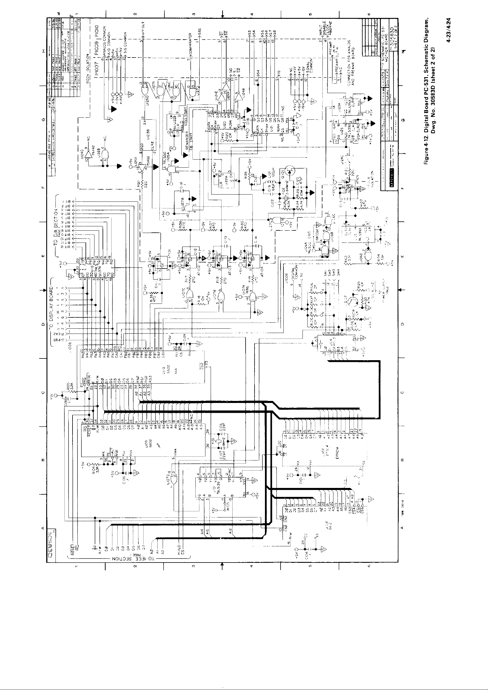
1
CI
Page 40

SERVICE FORM
Model No.
Serial No. Date
Name and Telephone No.
Company
List all control settings, describe problem and check boxes that apply to problem.
q
q
Intermittent
q
IEEE failure
OFrant panel operational DA11 ranges or functions are bad
Display or output (circle one)
aDrifts
[7Unstable
q
Overload
q
Calibration only
q
Data required
(attach any additional sheets as necessary.)
Show a block diagram of your measurement system including all instruments connected (whether power is turned on or not)
Also, describe signal source.
Analog output follows display
q
Obvious problem on power-up
q
Unable to zero
q
Will not read applied input
DC of C required
q
Particular range or function bad; specify
q
Batteries and fuses are OK
q
Checked all cables
Where is the measurement being performed? (factory, controlled laboratory. out-of-doors, etc.)
What power line voltage is used?
Relative humidity?
Any additional information. (If special modifications have been made by the user. please describe.)
Other?
Ambient Temperature?
“F
Page 41

Model 1.81 Instruction Manual Addendum
Introduction
This addendum to the Model 181 Instruction Manual is being included in order to provide you with the latest in-
formation in the least possible time. Please read this information before using the Model 181.
Possible improper bus operation
Symptom: The Model 181 will not accept IEEE-488 commands.
Problem: Taking the Model 181 out of remote mode using the IEFIE48.1 Local command or issuing a Device Clear
may cause problems. This problem appears to occur only with the National InAnments PCII and PCIIA IEEE-488
interface card software drivers. It has not been observed when using Rev. 2.11 of the CEC IEEE-driver or with Rev.
2.6 of the IOTech IEEE-488 bus driver, but the possibility of the problems occurring
ruled out.
Solution: The Model 181 must be put back in the remote mode after sending Device Clear or Go to Local before any
other IEEE commands will be accepted.
with these interfaces cannot be
Programming examples
National Instruments PCII and PCIIA Example
’ UNCLUDE: ‘qbdecl.bas’
CALL IBPINlJ (“GPIBO”, IBO%)
CALL IBPIND (“KIlSl”, KIlSl%)
CALL IBSIC (IBO%)
CALL IBSRE uBo%, 1)
CALL IBCLR KIlSl%)
CALLIBLOC (KI181%)
’ MUST ISIJE THESE COMMANDS
’ OR ELSE YOU WILL HAVE TO TOGGLE THE POWER ON THE 181 TO RECOVER.
CALL IBSRE (lBo%, 1)
CALL IBCMD (IBO%, “?%?“) ’ send UNL LISTEN 5 UNL to 181
BEFORE SENDING ANY COMMANDS
To THE l&31!
32421-B-1 / 12-91
Page 42

(see Table 1 for LISTEN commands at other IEEE Addresses)
Table 1. Listen command characters
ASCII Equivalent listen commands
‘
SPACE
LISTEN 0
0 LISTEN 16
i
1 LISTEN1
I, LISTF.N 2
# LISTEN 3
$ LISTEN 4
%
&
LISTEN 5
LISTEN 6
LISTImI 7
( LISTEN 8
LISTFN9
)
I LISTFN10
+ LISTEN11 ;
LISTFN12 <
LISTFN13 =
LISTEN14 >
/
LISTBN15 ? IJNL
1 L.IsrEN 17
2 LISTEN 18
3 LISI-EN 19
4 LLSTEN 20
5 LISTEN 21
6 LIsrEN22
7 LISTEN23
8 LISTEN 24
9 LISTEN25
: LISTEN 26
LISTEN 27
Llsl-FN 28
LISTEN 29
LISTEN 30
I-o send a LISTEN 2 issue ‘?“+CHR$ (34) + “?”
CEC PC-488 card example
’ $INCLUDE: ‘IEEEQB.BI
’ CALL INITIALIzE01,0)
CALL TRANSMIT (“UNT UNL LISTEN 5 SIX UNL”, STATUS%) ’ clear 181
CALL TRANSMIT VJNL LISTEN 5 GI’L IJNL”, STATUS%) ’ Put 181 into Local
’ MAY HAVE TO ISSUE THIS COMMAND
’ OR ELSE YOU WILL HAVE TO TOGGLE THB POWER ON THE 181 TO RECOVER.
CALL TRANSMIT (“REN UNL LISTEN 5 UNL”, STATUS%)
BEFORE SENDING ANY CO-
TO THE 181!
Page 43

lOTech~Personal488 card example
OPEN “\DEV\IEEEOUT” FOR OUTPUT AS #I
OPEN “\DEV\IEEElW FOR INPUT AS #2
IOCTL #l, “BREAK”
IWNT #I, “RESFY
PRINT #1, “CLEAR 5”
PRINT #l, ‘uxAL 5”
MAY HAVE TO ISSUE THIS COMMAND
OR ELSE YOU WILL HAVE TO TOGGLE THE POWER ON THE 181 TO RECOVER.
PRINT #1, “REMOTE 5”
BEFORE SENDING ANY COMMANDS TO THE 181!
 Loading...