

Page 1

INSTRUCTION MAdUAL
Models 1792,6422
Isolated BCD Outputs
Keithley instruments, Inc.
28775 Aurora Road/Cleveland, Ohio 44139/(216) 248-0400
Page 2

WARRANTY
Keithley Instruments, inc. warrants this product to be free from defects
in material and workmanship for a period of 1 year from date of shipment. During the warranty period, we will, at our option, either repair
or replace any product that proves to be defective.
To exercise this warranty, write or call your local Keithley representative, or contact Keithley headquarters in Cleveland, Ohio. You will be
given prompt assistance and return instructions. Send the instrument,
transportation prepaid, to the indicated service facility. Repairs will be
made and the instrument returned, transportation prepaid. Repaired
products are warranted for the balance of the original warranty period,
or at least 90 days.
LIMITATION OF WARRANTY
This warranty does not apply to defects resulting from unauthorized
modification or misuse of any product or part. This warranty also does
not apply to fuses, batteries, or damage from battery leakage.
This warranty is in lieu of all other warranties, expressed or implied, in-
cluding any implied warranty of merchantability or fitness for a particular use. Keithley Instruments, Inc. shall not be liable for any indirect,
special or consequential damages.
STATEMENT OF CALIBRATION
This instrument has been inspected and tested in accordance with
specifications published by Keithley Instruments, Inc.
The accuracy and calibration of this instrument are traceable to the
National Bureau of Standards through equipment which is calibrated at
planned intervals by comparison to certified standards maintained in
the Laboratories of Keithley Instruments, Inc.
KEITHLEY INSTRUMENTS, INC.
INSTRUMENT DIVISION / 28775 Aurora Road / Cleveland, Ohio 44139 / U.S.A. / (216) 248-0400 / Telex: 98-5469
WEST GERMANY: Keithley Instruments GmbH / Heiglhofstr. 5 / 8000 Munchen 70 / (089) 710020 / Telex: 52-l 2160
GREAT BRITAIN: Keithley Instruments, Ltd. I 1, Boulton Road I Reading, Berkshire RG 2 ONL / (0734) 86-12-87/88 /Telex: 84-7047
FRANCE: Keithley Instruments SARL / 2, Bis Rue Leon Blum / B.P. 60 / 91121 Palaiseau Cedex / (6) 011-51-55 I Telex: 600-933
NETHERLANDS: Keithley Instruments BV / Arkelsedijk 4 / Postbus 559 / 4200 AN Gorinchem I (0) 1830-25577 / Telex: 24-684
SWITZERLAND: Keithley Instruments SA I Kriesbachstr. 4 / 8600 Dubendorf I 01/821-94-44 / Telex: 57-536
AUSTRIA: Keithley Instruments Ges.m.b.H. / Doblinger Haupstr. 32 / 1190 Wien / 314 289 / Telex: 13-4500
Page 3

MODELS 1792, 6422
I SOLATED BCD OUTPUTS
Copyright 1979, Keithley Instruments, Inc.
Third Printing, May 1981, Cleveland, Ohio
U.S.A.
Document No. 30155, Rev. B
Page 4
TABLE OF CONTENTS
SECTION TITLE
PAGE
1.
GENERAL INFORMATION ................... l-l
l-l.
INTRODUCTION ...................... l-l
l-3. COHPATIBILITY. ..................... l-l
l-5. WARRANTY INFORMATION .................. l-l
l-7. CHANGE NOTICES ..................... l-l
l-9.
SAFETY SYMBOLS ..................... l-l
l-11. SPECIFICATIONS ..................... l-l
2. INITAL PREPARATION ...................... 2-l
2-l. INTRODUCTION ...................... 2-l
2-3.
UNPACKING AND INSPECTION ................ 2-l
2.5.
PREPARATION FOR USE. .................. 2-l
2-7. MODEL 1792 INSTALLATION. ................ 2-3
2-9. Fidel 1792 Output Connections. ............ 2-3
2-11. IIODEL 6422 INSTALLATION. ................
2-4
3.
GPERATION ....................... .3-l
3-l.
INTRODUCTION ...................... 3-l
3-3.
OVERALL OPERATION. ...................
3-l
3-9. CIRCUIT DESCRIPTION. .................. 3-3
3-11.
Control Circuitry. ..................
3-3
3-14
Switching Circuitry. ................. 3-4
3-16.
Isolator Network ................... 3-4
3-18.
Busy/Hold Circuit. .................. 3-4
3-20.
Output Registers And Buffers ............. 3-5
3-22. DC-to-DC Converter .................. 3-5
3-24 TEST POINT DATA. .................... 3-5
3-26.
SPECIAL HANDLING OF STATIC SENSITIVE DEVICES ......
3-6
4.
REPLACEMENTPARTS ...................
4-l
4-l. GENERAL. ........................ 4-l
4-3.
ORDERING INFORMATION ..................
4-l
4-5.
SCHEMATIC. ....................... 4-l
4-7.
COM’ONENT LAYOUT ....................
4-l
I LLUSTRATI GNS
FIGURE
TITLE PAGE
2-l
Installation of Model 1792 ............... 2-2
2-2
Installation of Model 6422 ............... 2-5
3-1
Model 1792/6422 Block Diagram. ............... 3-l
3-2
Timing Diagram ..................... 3-2
3-3
Ring Counter and Gating. ................ 3-3
3-4
Busy/Hold Circuit. ................... 3-4
Page 5
UODELS 1792, 6422
SECTION 1 GENERAL lNFGRMATI(%
GENERAL INFORMATION
l-l. I NTRODUCT I ON.
l-2.
The Models 1792 and 6422 are isolated BCD
output options that convert displayed meter readings
to electrically isolated, latched, and buffered peral lel 8CD outputs.
These can be appl ied to I ine
printers or other external data hand1 ing equipment.
Logic
levels are TTL/DTL and CMOS compatible.
Output data includes sign and overrange signals. In
addition,
a BUSY control I i ne indicates that the
meter is updating data.
The trailing edge of this
signal is normally used to initiate a print or load
operation at the listening device. An input control
I ine (HOLD) al lows the listening device to inhibit
the update of output data. When this line is high,
the data update rate is the same as the meter
conversion rate,
typically 2.5 readings/second.
Operating characteristics for the Models
6422 and
1792 are given in their respective Specification
Tables (Table l-l and l-2).
Both options can be
either factory or field installed.
Separate
installation procedures are provided in this manual,
because of the different mounting and output cabling
provisions of the options.
l-3. CGf+‘ATIBILITY.
l-4.
The Model s 1792 and 6422 interface options
are
compatible with the following Keithley
I nstr unents:
Model 6422
Model 642 Electrometer Serial Nunber 53402A and
above.
Mode I 1792
Model 179 DMFl Serial Nunber 20000 and above.
Model 179-20A DMFl all Serial Numbers.
Model 177 DMM Serial Nunber 14500 and above.
Model 480 Picoammeter Serial Nunber 12000 and
above. Note:
First 3-l/2 digits at BCD auf-put
same as Model 480 display.
l-5.
WARRANlY INFGRMATIOIJ.
l-6.
The Warranty is given on the inside front
cover of this Instruction Manual. If there is a
need to exercise the warranty, contact the Keithley
Representative in your area to determine the proper
action to be taken.
Keithley maintains service facilities in the United Kingdom and West Germany, as
well as in the
United States. Check the inside
front cover of this Manual for addresses.
l-7.
CHANGE NOTICES.
l-8.
Improvements or changes to the equipment which
occur after printing of the Instruction Manual will
be explained on a Change Notice sheet attached to
the inside back cover.
l-9. SAFETY SYMOBCLS
l-10.
Safety symobls used in thls manual are as
fol lows:
IM3oRTANT
The ! n symbol can be found in various places in
this manual. Careful ly read the associated CAUTION statements with regard to proper use and
handling of the equipment. Damage to the equip-
ment may occur if these precautions are ignored.
t
This
symbol can be found In various places in
this manual.
This symbol indicates those areas on
the equipment which are potential shock hazards.
Careful ly read the associated WARNING statements
with regard to proper use and hand1 Ing of the
equipment.
Serious personal injury may result if
these precautions are ignored.
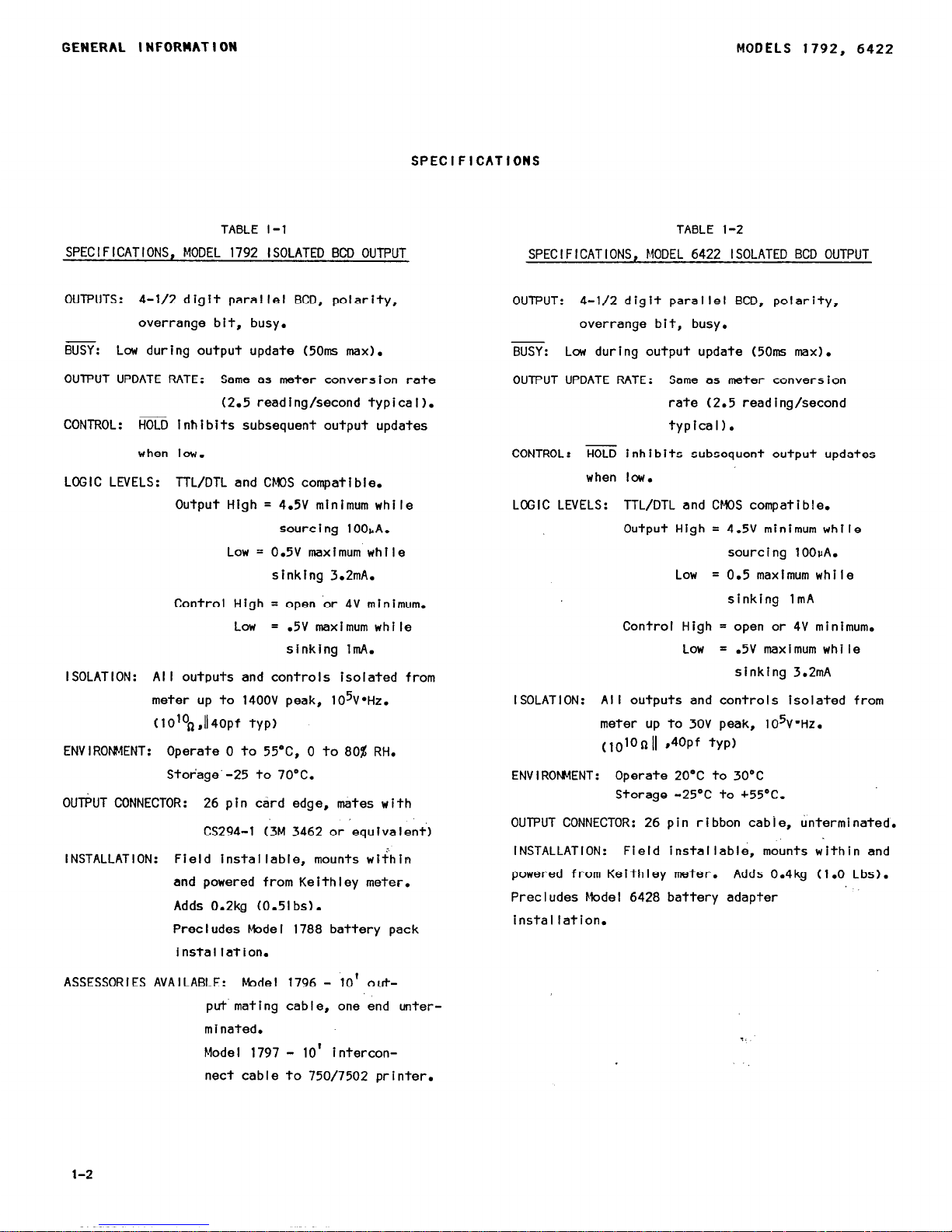
1-11. SPECIFICATIONS.
l-12.
Detailed specifications for the Model 1792
and 6422 are given
In Tables l-l and 1-2,
respectively.
l-l
Page 6
GENERAL INFORMATION
MODELS 1792, 6422
SPECIFICATIONS
TABLE I-1
SPECIFICATIONS, MODEL 1792 ISOLATED BCD OUTPUT
OUTPUTS : 4-l/2 digit parallel BCD, polarity,
overrange bit, busy.
BUSY:
Low during output update (5Oms max).
OUTPUT UPDATE RATE:
Same as meter conversion rate
(2.5 reading/second typical).
CONTROL : E inhibits subsequent output updates
when low.
LOGIC LEVELS: TTL/DTL and CMOS compatible.
Output High = 4.5V minimum while
sourcing lOOkA.
Low =
0.5V maximum while
sinking 3.2mA.
Control High = open or 4V minimum.
Low =
.5V maximum while
sinking 1mA.
ISOLATION:
All outputs and controls isolated from
meter up to 1400V peak, 105V*Hz.
(lOlO, ,ll40pf typ1
ENVIRONMENT: Operate 0 to 55”C, 0 to 805 RH.
Storage’ -25 to 7O’C.
OUTPUT CONNECTOR:
26 pin card edge, mates with
CS294-1 (3M 3462 or equivalent)
INSTALLATION: Field installable, mounts within
and powered from Keithley meter.
Adds 0.2kg (0.51 bs).
Precludes Mode I 1788 battery pack
installation.
ASSESSORIES AVAILABLE: Model 1796 - 10’ ou-t-
put mating cable, one end unter-
minated.
Model 1797 - 10’ intercon-
nect cable to 750/7502 printer.
TABLE l-2
SPECIFICATIONS, MODEL 6422 ISOLATED BCD OUTPUT
OUTPUT:
4-l/2 digit parallel BCD, polarity,
overrange bit, busy.
BUSY: Low during output update (50111s max).
OUTPUT UPDATE RATE:
Same as meter conversion
rate (2.5 reading/second
typical).
CONTROL : HOLD inhibits subsequent output updates
when low.
LOGIC LEVELS:
TTL/DTL and CF%X compatible.
Output High = 4.5V minimum while
sourcing lOOpA.
Low = 0.5 maxlmum while
sinking 1 mA
Control High = open or 4V minimum.
Low = .5V maximum while
sinking 3.2mA
I SOLAT I ON :
All outputs and controls isolated from
meter up to 30V peak, 105VoHz.
(lolon II ,4OPf tYP)
ENVIRONMENT:
Operate 20°C to 30°C
Storage -25°C to +55’C.
OUTPUT CONNECTOR: 26 pin ribbon cable, unterminated.
INSTALLATION:
Field installable, mounts within and
powered from Keithley meter. Adds 0.4kg (1.0 Lbs).
Precludes Model 6428 battery adapter
installation.
l-2
Page 7
MODELS 1792. 6422
SECTION 2. INITIAL PREPARATION.
INITIAL PREPARATION
2-l. INTRCOUCTION.
2-2.
This section provides information for r(ncomlng
inspection and preparation for use of your Model
1792/6422 BCD output option.
2-3.
UNPACKING AND INSPECTION.
2-4. The Model 1792/6422 was careful ly inspected,
both mechanically and electrically before ship-
ment.
Upon receiving your BCD output option, unpack all items from the Sh i ppingcontainer and
check for any obvious damage which may have occured during transit.
Report any damages to the
shipping agent. Retain and use the original
packaging materials if reshipment is required.
The following items (Keithley Part No. in parentheses) are shipped with al I orders of your
option:
Model 1792
a - PC-498 and shield Assembly
1) PC-488 Assembly (29961D)
2) Shield Assembly (30108C)
b.
-
Replacement Top Cover (30136C)
c. A copy of this Instruction Manual (30155)
d. - Separate Optional Cable (Model 1796 or
1797), as ordered.
Model 6422
a. Assembled PC Board (299610) with modif ied PC-
498 (301658).
b.
Shield (301328).
-
5 Output Cable assembly with back panel and
strain rel iefs.
I) Cable assembly (302348-l)
2) Back panel (301318).
3) Two strain reliefs (27686A).
-. Mounting Hardware
d
I) Eight Standoffs (ST-94).
2) Eight 6-32 X 5/16” screws.
8. - A copy of this Instruction Manual (30155).
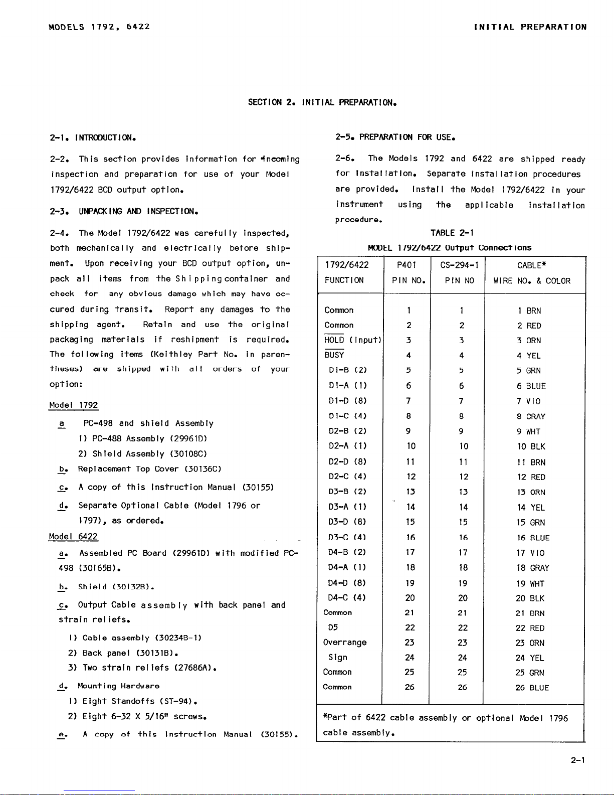
2-5. PREPARATION FOR USE.
2-6. The
Models 1792 and 6422
are
shipped ready
for installation.
Separate installation procedures
are provided.
Install the Model 1792/6422 in your
instrument using
the
appl icable
installation
procedure.
TABLE 2-l
MODEL 1792/6422 Output Connections
1792/6422
P40 1 cs-294- 1 CABLE*
FUNCTION
PIN NO.
PIN NO
WI RE NO. b COLOR
Common
1 1 1 BRN
Common
2 2 2 RED
HOLD ( Input)
3 3 3 ORN
BUSY
4 4 4 YEL
Dl-B (2)
5 5 5 GRN
Dl-A (1)
6 6 6 BLUE
Dl-0 (8)
7 7 7 VI0
01-C (4)
8 8 8 GRAY
02-B (2)
9 9 9 WHT
02-A (1)
10 10 10 BLK
02-D (8)
11 11 11 BRN
02-C (4)
12 12 12 RED
03-B (2)
13 13 13 ORN
’
D3-A (1)
14 14 14 YEL
D3-D (8)
15 15 15 GRN
D3-C (4)
16 16 16 BLUE
04-B (2)
17 17 17 VI0
04-A (1)
18 18 18 GRAY
04-D (8)
19 19 19 WHT
D4-C (4)
20 20 20 BLK
Common
21 21 21 BRN
05
22 22 22 RED
Overrange
23 23 23 ORN
Sign
24 24 24 YEL
Common
25 25 25 GRN
Common
26 26 26 BLUE
*Part of 6422 cable assembly or optional Model 1796
cable assembly.
2-l
Page 8
\NITIAL PREPARATION
MODELS 1792, 6422
CARD-EDGE .
CONNECTOR
PIN 2 (TOP)
PIN 1 (UNDERNEATH)
,-Model 1792
I I
-
;+ \P1?08
PL
\GROUNF CLIP :
1
ASTIC SPACER
(4 PLACES)
1792-0023-A
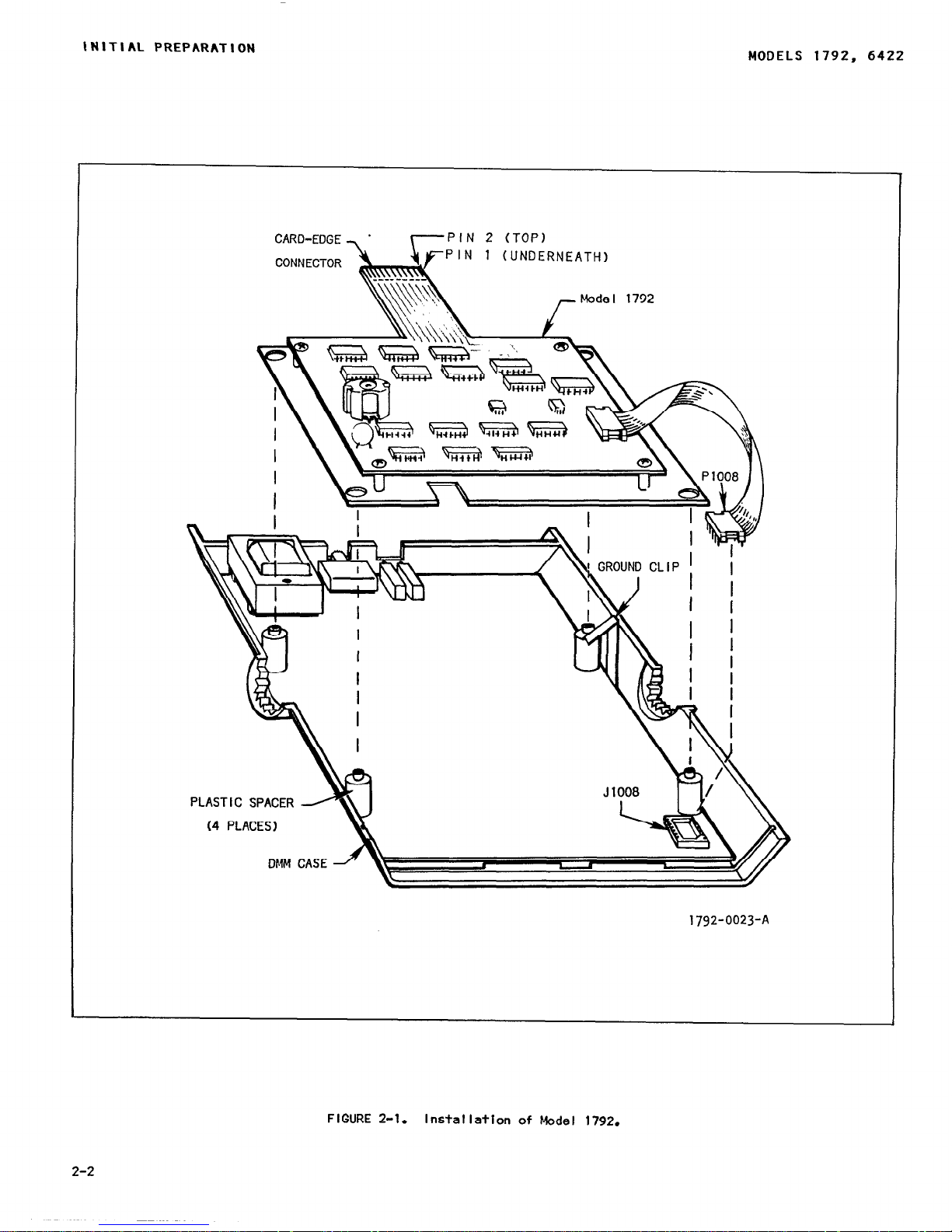
FIGURE 2-l.
Installation of Model 1792.
2-2
Page 9

MODELS 1792, 6422
INITIAL PREPARATION
2-7. MODEL 1792 INSTALLATION
2-8.
The Model 1792 is installed internally in the
Model 177, 179, 179-20A, or 480 and is powered by
the instrument% line operated power supply. Instal-
lation of the Model 1792 precludes use of the Model
1788 Battery Pack.
Refer to Figure 2-1 and install
the Model 1792 as fol lows:
‘t
WARN I NC
Disconnect the line cord before removing the
case cover.
a. Turn off power and disconnect line cord.
b.
-
Turn the DMM bottom side up and loosen the
four screws in the bottom cover.
c. Hold the top and bottom covers together to pre-
vent their separation and turn the DMM over to the
normal position.
d.
-
Lift off the top cover and the calibration
shield if installed.
If the Model 1788 Battery
Pack is installed,
disconnect its connector from
the plug on the main printed circuit board and
remove the Model 1788. The four plastic spacers
must remain in place on the upright studs project-
ing through the main printed circuit board.
NOTE
Do not
discard the calibration
shield.
This shield must be installed during caiibrat ion,
as described in the Instruction Manual
for your instrument.
e. - If the Model 1788 was removed, set the LINE/
BAT switch on the main printed circuitboard to the
LINE position.
f
-*
Connect P1008 to its mating recepticle on the
printed circuit board (J1002 on the Model 480
and J1008 on the Models 177, 179 and 179-20A).
9
Install the Model 1792 in the instrument so that
it rests on the plastic spacers.
The ground clip
must make contact with the upper side of the shield
on the Model 1792.
h
-0
Install the top cover that was shipped with
the Model 1792. Th is cover has a s lot to
accommodate the card edge
connector of the Model
mm
i1rL.c ~
AL-
Save all removed parts for reinstallation In
the event that the 1792 is to be removed at a
I ater date.
2-9.
Model 1792 Output Connections.
2-10.
The Model 1792 uses a 26 pin card-edge
connector (P401) to provide all input and output
connections to external equipment. This connector
mates with a Keithley CS-294-1 flat-ribbon connector
(3M 3462 or equivalent), which is not supplied.
The output connector pins are identified in Table
2-l.
Two optional cable accessories are available for interfacing the Model 1792 with external equipment.
The Model 1796 is a 10 foot (3 meter) flat ribbon
cable with 26 wires and an output mating connector
(CS-294-l) on one end.
The other end is left
unterminated so that a connector can be installed
that is compatible with the equipment to be
interfaced.
Pin identification for the Model 1796
is the same as that given in Table 2-l for the Model
1792 output connector.
The wires are color coded
with the brown wire to pin 1, the red wire to pin 2,
and so on.
The Model 1797 is a 10 foot -(3 meter) cable that
provides the connections to interface the Model 1792
with the Keithley 750/7502 Line Printer.
This cable
is plug-to-plug compatible with both the Model 1792
and Hodel 750/7502 for easy installation. Table 2-2
identifies the cable connector pins and wires.
2-3
Page 10

INlTlhL PREPARATION MODELS 1792, 6422
2-11. MODEL 6422 INSTALLATION
2-12.
The Model 6422 is installed internally in the
Model 642 and is powered by the Model 642 line operated power supply. Installation of the Model 6422
precludes the use of the Model 6428 Battery Adapter
option. Refer to Figure 2-2 and instal I the Model
6422 as follows:
t
WARNING
Disconnect the line cord before removing
the case cover.
a. Turn off power and disconnect the I ine cord.
b.
Remove the four attaching screws and remove
-
the top cover.
c. Remove the two attaching screws from the plate
-
(or Model 6428) on the rear panel of the mainframe. If the
Model 6428 is installed, remove
it as foi lows:
I) Disconnect the connector from the plug
on the mother board.
2) Remove the attaching screw and spacer, and
remove the Model 6428 through the opening in
the rear panel.
d.
Remove the front four attaching screws from
the mother board and replace them with the metal
spacers, as shown in Figure 2-2.
These spacers
may fit snugly and require use of a wrench to in-
stall them.
Take care not to cross thread or
tighten them too tight.
8.
Connect P1008 to 51013 on the mother board.
After making the connection, place the printed
circuit board outside of the Model 642 so that
there is no strain on the cable and the board will
be out of the way during installation of the
shield and spacers in the following steps.
f.
Place the shield on the spacers and attach
with the four screws, as shown.
The printed circuit board will not fit properly unless the
shield is installed with the nut plates on the
bottom side and with the hole pattern positioned
as i I I ustrated.
I-.
Install the four spacers into the shield.
h.
Place the printed
circuit board on the
spacers (component side down) and attach it with
four screws.
i
-*
Connect the output cable to the card-edge connectar and attach the assembly to the rear panel
of the mainframe with the two screws removed in
step c above.
L*
Reinstall the case top cover.
k.
Connect the Model 6422 to your equipment by
installing an appropriate connector on the un-
terminated end of the cable.
Pin identification
for the Cable assembly connector is the same as
that given in Table 2-l for the Model 1792/6422
output connector.
The wires are color coded with
the brown wire to Pin 1, the red wire to pin 2,
and so on.
L-
Save all removed parts for reinstal iation in
the event that the Model 6422 is to be removed at
a later date.
2-4
Page 11

MODELS 1792, 6422
INITIAL PREPARATION
MOD I F I ED PC-498
(30165B)
STANDOFF (8)
MAINFRAME
6422-0032-B
ASSEMBLY
FIGURE 2-2.
Installation of Model 6422
2-5
Page 12

INITIAL PREPARATION
MODELS 1792. 6422
1792
FUNCTION
cs-294- 1
PIN NO.
Common
1
Common
2
HOLD (Input)
3
BUSY 4
Dl-B (2)
5
Dl-A (1) 6
Dl-D (8) 7
Dl-C (4) 8
D2-B (2) 9
D2-A (1) 10
02-D (8)
11
D2-C (4) 12
D3-B (2) 13
03-A (1) 14
D3-D (8)
15
D3-C (4) 16
D4-B (2) 17
D4-A (1)
18
D4-D (8)
19
04-C (4)
20
Common 21
05 22
OVERRANGE
23
SIGN 24
Common
25
Common 26
TABLE 2-2
Model 1797 Cable Connections
CABLE
WIRE NO.
AND COLOR
CS-27 1
PIN NO.
1 BRN
9
2 RED
14
3 ORN
15
4 YEL
13
5 GRN 2
6 BLUE
18
7 VI0
37
8 GRAY
19
9 WHT
22
10 BLK
5
11 BRN
23
12 RED
6
13 ORN
39
14 YEL
38
15 GRN 41
16 BLUE
40
17 VI0
24
18 GRAY
7
19 WHT
25
20 BLK 8
21 BRN 43,44,45
22 RED
42
23 ORN
11
24 YEL
10
25 GRN 12
26 BLUE
28,29
750/75op
FUNCTION
*Pr i nter Format
10 9 8 7 6 5 4 3 2 1 Column
8-l gnd.
Common
HOLD (Output)
EXTERNAL PRiNT
3-2
3-l
3-8
3-4
4-2
4-l
4-8
4-4
5-2
5-l
5-8
5-4
6-2
6-l
6-8
6-4
7-2,7-4,7-8 gnd.
7-l
10-l
8-4
10-4 gnd.
10-8, I O-2 gnd.
O=On Scale
L
l=Overrai+
SIGN
(+implied)
2-6
Page 13

MODELS 1792, 6422
OPERATION
SECTION 3. OPERATION.
3-1. INTRODUCTION.
pulse and divides the lOOkliz CLOCK by ten to pro-
3-2.
This section describes operation of the Model
1792/6422.
Except where noted, the descr lptions
apply to both models.
The information is arranged
to provide overall operation, circuit descriptions,
test point data and special handling requirements
for static sensitive devices.
3-3.
OVERALL OPERATION.
duce the 1OkHz SYNC train. The ring counter output
drives the switching to convert the multiplexed BCD
digit data into a serial one bit format. The digit
five (D5) line is decoded to serialize the SIGN and
OVERRANGE I ines.
3-6.
The isolating network consists of two optocouplers and buffers. The SYNC and DATA pul ses
are transmitted with the opto-couplers normally off
3-4. Figure 3-l shows the Model 1792/6422 in block
diagram form.
The 1792/6422 operates by first converting multiplexed BCO input data into synchronous
serial data.
Serial data is then transmitted across
to conserve power.
3-7.
The SYNC train after transmission goes into a
BUSY/HOLD network which controls the output shift
reg i ster. This network consists of a flip-flop, one
an opto-electric coupler network and loaded into a
twenty bit shift register.
Data is then buffered
and appears at the output in parallel BCD format.
3-5.
The STROBE and CLOCK lines come from the meter
motherboard and provide timing for the 1792/6422.
The control
consists of a divider and a ring
counter. The divider is phase-locked to the STROBE
shot, and gating.
The BUSY output goes low during
data update. However,
if the HOLD I ine is low, no
data wiil be ioaded, and the output wiii not change.
With the HOLD line high, data is updated at the
meter
conversion rate,
typically 2.5 readings/
second.
OUTPUT COMMON
Figure 3-l.
Model 1792/6422 Block Diagram
3-l
Page 14

OPERAT I ON
MODELS 1792, 6422
GNO +-
I
SYNC
I
mu uuuu uuuu luuu
uuuu urn
50
USE&+-
I’
I”
//
100
-!
I
r ZC
I
II
I
7 y uSEC
I I
I
I
II
I
II DATA I
I
BUSY -
I
I
L
4
~380 mSEC
I
3
I
I
I
I
HOLD
7
sl-
I
-4
’
+--2p SEC MIN.
d +t--20DnSEC iii hi. ~ ~
DON’T CARE
I
I
I ~
c- +5v
I
4
= 20 mSEC COMMON
I
l
I
FLAG
I
11 1 I I ’ 1 I I I 1
SYNC
II I I I 1 I I I I I
I
1
-
I
SHIFT
CLOCK
I-*-- *--- .--- *--- au--
f
I
II
1 1 1 I I I
’ I I
I I
I 1 I I I I
I
I
I
I
I
I
I
I
I
t5v
I
I
STROBE
I
I
2mSEC
4
39DmSEC
L
1792-0033-A
FIGURE 3-2.
Timing Diagram.
3-2
Page 15

MODELS 1792, 6422
OPERATION
3-a.
Input power is furnished by the host meter
(+5V for the Model 1792 and t6V for the Model
6422).
The power for the isolated (output) side is
provided by a DC-to-DC converter running at lOOkliz.
3-9.
CIRCUIT DESCRIPTIONS.
3-10.
This section provides detailed descriptions
of the major circuit blocks described in Overall
Operation of the Model 1792/6422. The descriptions
are referenced to the Model 1792/6422 (schematic
299650,
Page 4-4).
Where necessary, simi pl if led
schematics are also provided.
Timing is shown in
the Model 1792/6422 Waveform Diagram (Figure 3-2).
3-11.
Control Circuitry.
3-12.
The control
consists of a divide-by-ten
counter (U414) and a ring
counter (U41lA) with
gating.
U414 divides the 1OOkHz CLOCK by ten to
produce 1OkHz optional transmission of the DATA and
SYNC tral ns across the opto-electric couplers.
The
STROBE pulses phase-lock the counter by presetting
it to 2 on each pulse.
Th 1 s ensures synchronous
long term operation.
3-13.
A simpl i fled schematic of the ring counter
and gating Is given in Figure 3-3.
Each STROBE
pulse enables the transfer of one digit (four bits)
one bit at a time. There are five STROBE pul ses in
each complete data transfer.
In operation, the
STROBE pulse sets the latch comprised of U415A and
U415B, enabl ing U415D to gate the 1OkHz SYNC pulses
to the opto-electric coupler and to the CLOCK input
of U411A.
U41lA gates a elll in sequence on its
4
output lines Ql through Q4 to drive the quad switch
and serialize the digit data.
U415C resets the
latch when the Ql through Q4 I ines are clocked to
al I zeros,
and it remains in reset unti I the next
STROBE pulse. Since the latch is not reset until
U411A is clocked to al I zeros, a pulse of c- 500
nanoseconds is produced on the SYNC I ine after each
4 SYNC pul ses, but this is too fast to be acknow-
ledged by the opto electric couplers.
STROBE
To U41lB
HIGH l/2 CLOCK PULSE
AFTER 94 GOES HIGH.
TO QUAD SWITCH
(U4 13)
1792-0036-A
FIGURE 3-3.
Ring Counter and Gating.
3-3
Page 16

OPERAT \ ON MODELS 1792, 6422
3-14.
Switching Circuitry.
3-15.
Switching to serialize the input BCD data is
provided by U413 and U416A.
U413 is connected as a
4: 1 multi plexer.
One of its input lines is connected through to the DATA opt-o-electric coupler
when its respective control I ine is driven high by
the ring counter (U4llAI.
U4 16A is connected as a
dual 2:’ multiplexer, switching is controlled by the
digit 5 (D5) line.
The fifth digit is the most
significant digit and is transmitted first.
Since
it is always a nOw or a lllw, bits 2, 3 and 4 are not
needed and can be used to transfer other information.
When the D5 line is high, the overrange and sign
status is sent on bits 4 and 3, respectively.
Conversely,
when the 05 line is low, 88 and 84 for
digits 4 through 1 are sent.
3-16.
Isolator Network.
3-17.
The isolator network is comprised of two
optically coupled isolators, two transistors and
their associated biasing resistors.
The isolators
provide 101oD isolation and are normally off to
conserve power. The transistors invert the pulses
and serve both as wave shapers and low impedance
buffers into the high impedance CMOS circuits.
3-18. Busy/Hold Circuit.
3-19.
A simpl ifled schematic of the BUSY/HOLD cir-
cuit is given in Figure 3-4. The BUSY I ine always
goes low during a potential data transfer.
When
BUSY goes low, the f I ip-flop Is clocked and the HOLD
I ine checked to see
if a new data transfer is
desired. If the HOLD line is high, the FLAG is set,
enabl ing U409D to gate the SYNC pul se train.
The
BUSY line
remains
low
for
approximately 20
mi I I iseconds.
When the BUSY I ine returns high, it
resets the fl ip-f lop and no data transfer can occur
until it goes low again. This will occur when the
one-shotmultivibrator
is triggered by the first-
pulse of the next SYNC train.
SYNC CLOCK I NG TO
OUTPUT SHIFT REGISTERS.
HOLD
BUSY
*U404 and U408 PROVIDE -400 NANOSECOND
DELAY TO ENSURE THAT FF RESET LINE IS LOW
BEFORE CLOCKING.
1792-0035-A
FIGIURE 3-4.
Busy/Hold Circuit.
3-4
Page 17

MODELS 1792, 6422
OPERATION
3-20. Output Registers And Buffers.
3-21. Five 4-stage serial-input/paral lel-ouiput
registers are connected together to form the twenty
bit output shift register. Serial input data is ap-
plied to the lrD1t input of U407A. Data is set up on
the fal I ing edges of the SYNC pulses and latched on
the rising edges. Data is shifted into the outpuf
shunts one half cycle of buffer drive and provides
optimal switching of 0403 to prodllce maximum voltage
in the secondary of the transformer.
R411 I imits
I imits the base current to 0403.
Power is pul sed
across transformer T401 and half- wave rectified by
CR401. Capacitor C401 and voltage regulator VR401
provide a stable positive five volt supply to the
isolated circuits.
register in a seq uBnce that can be determined by
reading the output line identification from top to
3-24. TEST POI NT DATA.
bottom on Schematic 29965D, page 4-4.
After data
transfer is complete, the display information is
available at the oufput card-edge connector in a
buffered parallel BCD format.
3-22. DC-to-DC Converter.
3-23.
The 1OOkHz clock is buffered by U410 and
applied to switching transistor 0403. 0 i ode CR402
3-25. The Model 1792/6422 has ten test points that
can be used for trocbl eshoot I ng or confidence test-
ing. Test point signals are described in Table 3-l.
The test points are accessible by removing the
instrument top cover as described in the applicable
instal lation procedure (i.e, Para. 2-l for Model
1792 or Para. 2-11 for Model 6422).
TABLE 3-l.
Test Point Data
Test
Point
TP’
TP2
TP3
TP4
TP5
TP6
TP7
TP8
TP9
TP’O
Signal
Reference
1OkHz. Clock, SVpp, 50% duty cycle
TP3
SYNC (See Timing Diagram Figure 3-l).
TP3
Digital non-isolated common, OV reference
for TPl and TP5.
Non-isolated positive supply from meter
(6V f 5% Model 6422 and 5V f 5% for Model
1792).
TP3
DATA (See Timing Diagram Figure 3-l).
TP3
Complement of TP2.
TPlO
Isolated DATA, same as TP5.
TP’O
Isolated t5V f 0.25V.
TP’O
SYNC SHIFT CLOCK-If HOLD is high,
same as TP2.
If HOLD is low, +5V (high).
See Timing Diagram Figure 3-l.
Isolated common, OV reference for TP6 thru
TP9.
3-5
Page 18

OPERAT I ON
MODELS 1792, 6422
3-26.
SPECIAL HANDLING OF STATIC
SENSITIVE DEVICES.
3-27. CMCS devices are designed to function at
very high impedance levels for low power consumpt ion. For this reason, a normal static charge build
up on your person or clothing can be sufficient to
destroy these devices.
The fol lowing steps I is-t the
static sensitive devices In your Model
1792/6422,
and provide instructions on how to avoid damaging
them when they must be removed/replaced.
a. Static sensitive devices:
Keithley
Reference
Part Number
Designation
IC-107
U401-U404 ,U408
IC-136
u405-u407 ,u411
IC-102
u409, u415
IC-106
u410
IC-105
U412
IC-221
u413
IC-145
u414
I c-222
U416
b.
The above integrated circuits should be
handled and transported only In protective con-
ta i ners. Typically they wil I be received in metal
tubes or static protective foam. Keep the devices
in their original containers until ready for use.
C.
-
Remove the devices from their protective contalners only at a properly grounded work bench or
table, and only after grounding yourself by using
a wrist strap.
d.
-
Handle the devices only by the body.
Do not
touch the pins.
NOTE
P1008 is shipped with a piece of conductive
foam covering the pins to prevent static
damage.
This conductive foam should be re
placed If you disconnect P1008 to remove
your BCD option from its host instrunent.
e. Any printed circuit board into which a device
-
I s to be inserted must al so be grounded to the
bench or table.
f. - Use only anti-static type solder suckers.
3-0
Use only grounded tip soldering irons.
h.
-
After soldering the device into the board,
or properly Inserting it into the mating recep-
tacle, the device is adequately protected and
normal hand1 ing can be resuned.
3-6
Page 19

MODELS 1792, 6422
REPLACEMENT PARTS
SECTION 4 REPLACEMENT PARTS
4-l. GENERAL.
4-2.
This section contains information for order-
ing replacement parts.
The Replaceable Parts List
(Table 4-2, Page4-2) is arranged in alphabetical
order of the Circuit Designations of the components.
A Cross-Reference List of Manufacturers, containing
their addresses,
is given in Table 4-l.
4-3.
DRDERING INFORMATION.
4-4.
To place an order,
or to obtain information
concerning replacement parts, contact your Keithley
representative or the Factory. See the inside front
cover for addresses.
When ordering, include the
following information.
a. Equipment Model Number.
b.
Part Description.
c. Circuit Designation (if applicable).
d.
Keithley Part Number.
-
4-5.
SCHEMATIC
4-6.
Model 1792/6422 BCD Option:
Schematic No. 29965D page 4 - 4.
4-7.
COFPDNENT LAYOUT.
4-8.
Physical location of the components is shown
in Component Layout No. 29961D, Pageq-5.
TABLE 4-l.
Cross-Reference of Manufacturers~
MFG.
CODE NAME AND ADDRESS
FED.
SUPPLY
CCQE
CLB
Centralab Division
Milwaukee, WI 53201
71590
F-l
FaIrchild Inst. Corp.
Mountain View, CA 94043 07263
ITT
Components
Lawrence, MA 15238
K-l Keithley Instruments, Inc.
Cleveland, Ohio 44139
88164
MEP Mepco, Inc.
Morrlstcwn, NJ 07960
8003 1
NAT
Nationa! Semi Corp.
Santa Clara, CA 95051
27014
NCI
Nationa I Components, Inc.
West Pal m Beach, FL
RCA RCA Corporation
Morrestown, NJ 08050
02734
T-l Texas I nstruments, Inc.
Dallas, TX 75231
01295
4-l
Page 20

REPLACEMENT PARTS
MODELS 1792, 6422
TABLE 4-2
REPLACEABLE PARTS LIST
/
/
I
I
I
I
I
I
I
I
I
I
I
I
I
I
I
I
I
I
I
I
I
I
I
I
Circuit
3es ig.
4T40 I
4T402
2401
c402
C403
D404
CR401
CR402
P1008
PI008
Q401
Q402
Q403
R40l
R402
R403
R404
R405
R406
R407
R408
R409
R410
R4 11
R412
R413
T401
u401
U402
u403
u404
u405
Location Mfr. Mfr. Keithley
Description
Sch. Pcb.
Code Des lg. Part No.
IC, Optical Iy-Coupled Isolator D-4 F-4 F-l
FCD 820 I C-82
IC, Optically-Coupled Isolator D-2 F-4 F-l FCD 820
I C-82
Cap, 4.7uF, 2OV, ETT
E-l D-4
NCI KNS475A020K c-179-4.7
Cap, 0.3311F, 2OV, ETT E-5
F-4 ITT
TAPA.33KZO
C-204- .33
Cap, O.luF, 16V, CerD
B-l
D-5
CLB UK16-104 C-238-. I
Cap, 0.3311F, 2OV, ETT
A-4
F-5
ITT
TAPA .33K20 C-204-.33
Diode, Si I icon, 75mA, 75V
E-l D-4 T-l lN914
RF-28
Diode, Si I icon, 75mA, 75V B-2 D-5 T-l lN914 RF-28
Cable Assembly (1792)
A-2 H-5 K-l --- 27961A-l
Cable Assembly (6422)
A-2 H-5 K-l --- 2796 l A-2
Transistor NPN Silicon D-4 E-4 T-l 2N3904 TG47
Transistor, NPN, Silicon
D-2
F-4 T-l
2N3904 TG47
Transistor, NPN, Silicon C-l D-5 T-l 2N3904 TG-47
lOKD,t5%, 1/4W, CarbF E-6 D-3
MEP CR25” R-76- 10K
lOOKR,*5%, 1/4W, CarbF E-5
F-4
MEP
CR2 5”
R-76- 1 OOK
lOKD,i5%, 1/4W, CarbF
E-3 E-4
MEP
CR25” R-76- 1OK
lOKD,k5%, l/4W, CarbF
E-2
F-4 MEP CR25”
R-76-10K
lOOKl2,*5%, 1/4W, CarbF
D-4
E-4 MEP
CR25”
R-76- 1OOK
lOOKG,k5%, 1/4W, CarbF
D-2
F-4 MEP CR25”
R-76- IOOK
39OO,i5%, 1/4W, CarbF
D-4 F-4 MEP CR25* R-76-390
3908,*5%, 1/4W, CarbF
D-3
F-4 MEP CR25” R-76-390
lOOKJ2,*5%, 1/4W, CarbF
D-5
F-4 MEP CR25” R-76- 1OOK
lOKn,f5%, 1/4W, CarbF
C-l D-5
MEP CR25” R-76- IOK
lKn,tS%, 1/4W, CarbF
B-l
D-5
MEP CR25” R-76- 1K
lOOKD,k5%, 1/4W, CarbF
D-4
E-4 MEP CR25” R-76-100K
lOOKn,k5%, 1/4W, CarbF
D-3
F-4 MEP CR25* R-76- 1OOK
Transformer, Power
D-l
D-4 K-l --- TR- 170
IC, CMOS, Hex Buffer
F-l ,E6
D-3
RCA CD4050AE 10107
IC, CMOS, Hex Buffer F-2,3 E-3
RCA CD4050AE IC-107
IC, CMOS, Hex Buffer
F-4
E-3
RCA CD4050AE
IC-107
IC, CMOS, Hex Buffer F-5,D-5
F-3
RCA CD4050AE IC-107
IC, CMOS, Duel 4-Stage Static Shift
Reg i ster.
F-1,2
D-4 RCA CD4015AE IC-136
*Manufacturers Des ignat ion includes Part Descr Ipt ion; e.g., CR25,
lOKP,*5%, 1/4W, CarbF for R40l.
4-2
Page 21

MODELS 1792, 6422
REPLACEMENT PARTS
TABLE 4-2 (CONT.1
REPLACEAEILE PARTS t fSf
Circuit
Desig.
U406
u407
U408
u409
u410
u411
U412
u413
u414
u415
U416
VR401
LocatIon
Mfr.
DescrIptiOn
scfa.
Pcb. Coda
IC, CMDS, Dual 4-Stage Static Shift
Reg i ster. F-3,4
E-4 RCA
IC, CMOS, Dual 4-Stage Static Shift
Register.
D-5,F-4
E-4 RCA
IC, CMOS, Hex Buffer
E-2,4,5,
F-4 RCA
IC, CMOS, Quad 2-Input NAND Gate
DE-4,5
F-4 RCA
IC, CMOS, Hex lnverter
ABCD-1,2,3,5 D-5
RCA
IC, CMOS, Dual 4-Stage Static Shift
Reg i ster.
CD-3
E-5 RCA
IC, CMOS, Dual 4-Input NOR Gate
B-4,A-5 E-5 RCA
IC, CMOS, Quad Analog/Digital Switch
C-5
F-5 NAT
IC, CMOS, Presettable Divide-by-N
Counter.
B-2 D-5
RCA
IC, CMOS, Quad 2-Input NAND Gate
BC-3,4 E-5
RCA
IC, CMOS, Quad 2 Channel Data Selector B-5
E-5 NAT
IC, 3-Terminal,
t5V Regu I ator f 5% E-l
D-4 NAT
Mfr.
Desig.
CD4015AE
CD4015AE
CD4050AE
CD401 1AE
CD4049AE
CD40 15AE
CD4002AE
CD40 16CN
CD4018AE
CD401 IAE
CD45 19BCN
LM78L05ACZ
Keith1.y
Part No.
IC-136
10136
IC-107
10102
IC-106
10136
10105
10221
10145
10102
I c-222
I C-223
4-3
Page 22

Sxa (u -
.
-- ----.
il.l.m’
8
Z’
1 I
-
4-4
Page 23

P
VI
Page 24

SERVICE FORM
Model No.
Name
Company
Serial No. P.O. No.
Phone
Date
Address
City
State
Zip
List all control settings and describe problem.
(Attach additional sheets as necessary. 1
Show a block diagram of your measurement system including all instruments connected (whether power
is turned on or not). Also describe signal source.
Where is the measurement being performed? (factory, controlled laboratory, out-of-doors, etc.)
What power line voltage is used? Variation?
Frequency? Ambient Temperature?
Variation?
OF. Rel. Humidity? Other?
OF.
Any additional information. (If special modifications have been made by the user, please describe below.)
*Be sure to include your name and phone number on this service form.
Page 25

KEITHLEY INSTRUMENTS, INC.
INSTRUMENT DIVISION I 28775 Aurora Road / Cleveland, Ohio 44139 / U.S.A. / (216) 248-0400 / Telex: 98-5469
WEST GERMANY: Keithley Instruments GmbH / Heiglhofstr. 5 / 8000 Munchen 70 / (089) 710020 / Telex: 52-12160
GREAT BRITAIN: Keithley instruments, Ltd. / 1, Boulton Road / Reading, Berkshire RG 2 ONL / (0734) 86-l 2-87/88 /Telex: 84-7047
FRANCE: Keithley Instruments SARL / 2, Bis Rue Leon Blum / B.P. 60 / 91 121 Palaiseau Cedex / (6) 01 1-51-55 I Telex: 600-933
NETHERLANDS: Keithley Instruments BV I Arkelsedijk 4 I Postbus 559 / 4200 AN Gorinchem I (0) 1830-25577 I Telex: 24-684
SWITZERLAND: Keithley instruments SA / Kriesbachstr. 4 / 8600 Dubendorf / 01/821-94-44 / Telex: 57-536
AUSTRIA: Keithley Instruments Ges.m.b.H. / Db’blinger Haupstr. 32 I 1190 Wien / 314 289 / Telex: 13-4500
 Loading...