

Page 1
SERVICE MANUAL
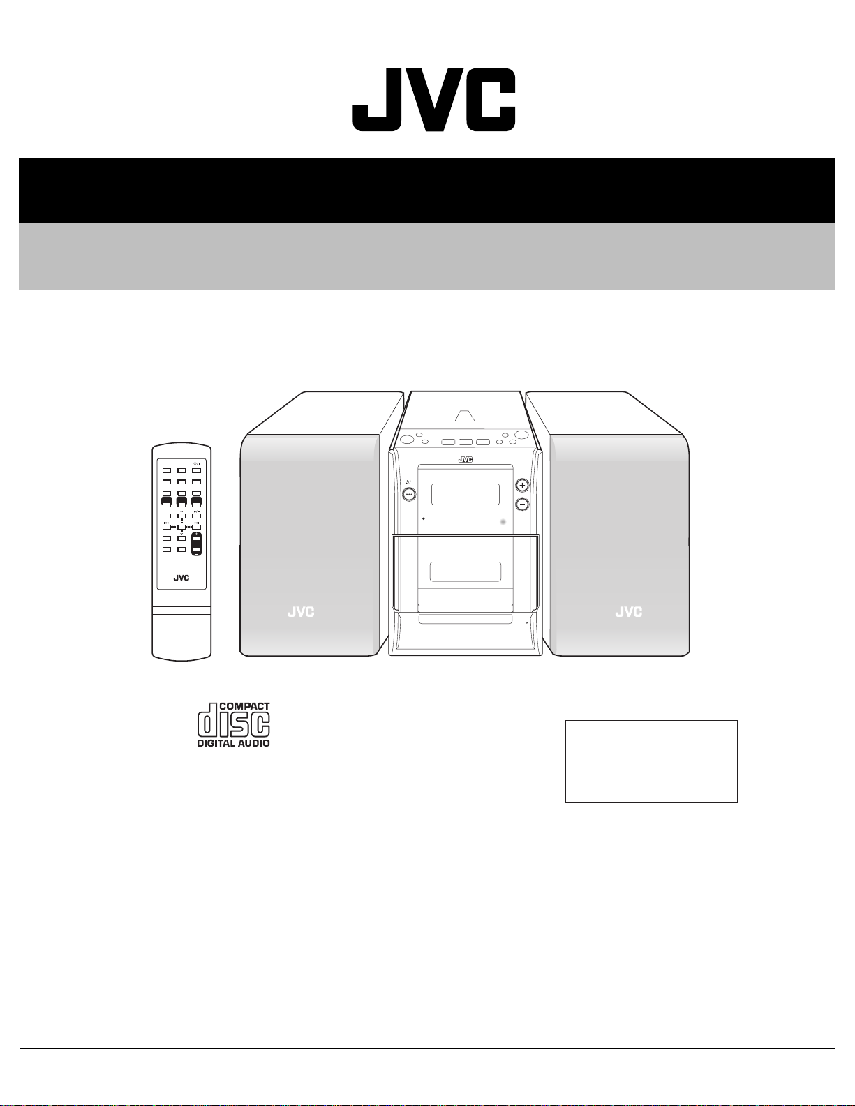
MICRO COMPONENT SYSTEM
MB06620041
UX-H10
TIMER
STANDBY/ON
TIMER SET
ON/OFF
RANDOM SLEEP
INTRO
REMAIN
TUNER
TAPE CD
/BAND
BEAT CUT
DISPLAY
/CLOCK SET
SOUND
MUTING
/BASS
REPEAT
ST/MONOPROGRAM
CD
VOLUME
STANDBY/ON
STANDBY
MICRO COMPONENT SYSTEM
UX-H10
VOLUME
RM-SUXH10U REMOTE CONTROL
CD SYNCHRO RECORDING
OPEN
Area Suffix
US ---------------- Singapore
UT ---------------------Taiwan
UW ---- Brazil,Mexico,Peru
TABLE OF CONTENTS
1 PRECAUTION. . . . . . . . . . . . . . . . . . . . . . . . . . . . . . . . . . . . . . . . . . . . . . . . . . . . . . . . . . . . . . . . . . . . . . . . . 1-3
2 SPECIFIC SERVICE INSTRUCTIONS. . . . . . . . . . . . . . . . . . . . . . . . . . . . . . . . . . . . . . . . . . . . . . . . . . . . . . 1-5
3 DISASSEMBLY . . . . . . . . . . . . . . . . . . . . . . . . . . . . . . . . . . . . . . . . . . . . . . . . . . . . . . . . . . . . . . . . . . . . . . . 1-6
4 ADJUSTMENT . . . . . . . . . . . . . . . . . . . . . . . . . . . . . . . . . . . . . . . . . . . . . . . . . . . . . . . . . . . . . . . . . . . . . . . 1-12
5 TROUBLESHOOTING . . . . . . . . . . . . . . . . . . . . . . . . . . . . . . . . . . . . . . . . . . . . . . . . . . . . . . . . . . . . . . . . . 1-16
COPYRIGHT © 2004 VICTOR COMPANY OF JAPAN, LIMITED
No.MB066
2004/1
Page 2

SPECIFICATION
Amplifier Section
CA-UXH10
Tuner FM tuning range 87.50 MHz-108.00 MHz
CD player Dynamic range 60 dB
Cassette deck Frequency response Normal (type I) 100 Hz-10 000 Hz
General Power requirement AC 110 V-127 V/ 220 V-240 V , adjustable with the voltage selector, 50 Hz/ 60 Hz
Speaker Section
SP-UXH10
Design and specifications are subject to change without notice.
Output Power (IEC 268-3) 10 W (5 W + 5 W) at 4 Ω (10% THD)
Speakers/Impedance 4 Ω - 16 Ω
AM tuning range AM 10 kHz intervals 530 kHz- 1 710 kHz
AM 9 kHz intervals 531 kHz-1 710 kHz
Signal-to-noise ratio 60 dB
Wow and flutter Immeasurable
Wow and flutter 0.35 % (WRMS)
Power consumption 22 W (at operation)
4.5 W (on standby)
Dimensions (W/H/D) (approx.) 145 mm × 209 mm × 226 mm
Mass (approx.) 2.6 kg
Type Full range bass-reflex type
Speakers 10 cm cone x1
Power handling capacity 5 W
Impedance 4 Ω
Frequency range 100 Hz to 15 kHz
Dimensions (W/H/D) (approx.) 135 mm × 209 mm × 152 mm
Mass (approx.) 1.3 kg each
1-2 (No.MB066)
Page 3
SECTION 1
PRECAUTION
1.1 Safety Precautions
(1) This design of th is product contains special hardw are and
many circuits and components specially for safety purposes. For continued protection, no changes should be made
to the original design unless authorized in writing by the
manufacturer. Replacement parts must be identical to
those used in the original circuits. Services should be performed by qualified personnel only.
(2) Alterations of the design or circuitry of the product should
not be made. Any design alterations of the product should
not be made. Any design alterations or additions will void
the manufacturers warranty and will further relieve the
manufacture of responsibility for personal injury or property
damage resulting therefrom.
(3) Many electrical and mechanical parts in the products have
special safety-related characteristics. These characteristics are often not evident from visual inspection nor can the
protection afforded by them necessarily be obtained by using replacement components rated for higher voltage, wattage, etc. Replacement parts which have these special
safety characteristics are identified in the Parts List of Service Manual. Electrical components having such features
are identified by shading on the schematics and by ( ) on
the Parts List in the Service Manual. The use of a substitute
replacement which does not have the same safety characteristics as the recommended replacement parts shown in
the Parts List of Service Manual may create shock, fire, or
other hazards.
(4) The leads in the products are routed and dressed with ties,
clamps, tubings, barriers and the like to be separated from
live parts, high temperature parts, moving parts and/or
sharp edges for the prevention of electric shock and fire
hazard. When service is required, the original lead routing
and dress should be observed, and it should be confirmed
that they have been returned to normal, after reassembling.
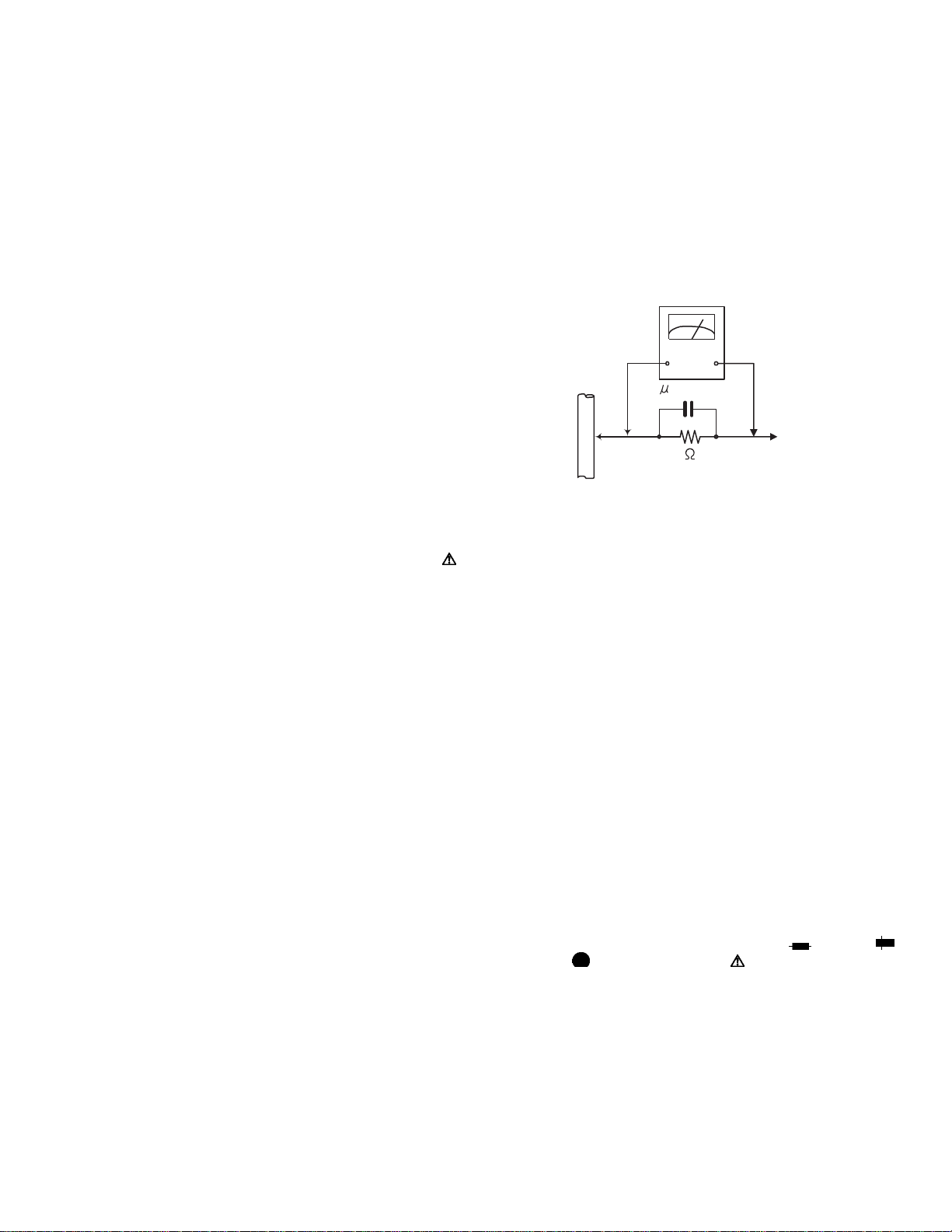
(5) Leakage shock hazard testing
After reassembling the product, always perform an isolation check on the exposed metal parts of the product (antenna terminals, knobs, metal cabinet, screw heads,
headphone jack, control shafts, etc.) to be sure the product
is safe to operate without danger of electrical shock.Do not
use a line isolation transformer during this check.
• Plug the AC line cord directly into the AC outlet. Using a
"Leakage Current Tester", measure the leakage current
from each exposed metal parts of the cabinet, particularly any exposed metal part having a return path to the
chassis, to a known good earth ground. Any leakage current must not exceed 0.5mA AC (r.m.s.).
• Alternate check method
Plug the AC line cord directly into the AC outlet. Use an
AC voltmeter having, 1,000Ω per volt or more sensitivity
in the following manner. Connect a 1,500Ω 10W resistor
paralleled by a 0.15µF AC-type capacitor between an exposed metal part and a known good earth ground.
Measure the AC voltage across the resistor with the AC
voltmeter.
Move the resistor connection to each exposed metal
part, particularly any exposed metal part having a return
path to the chassis, and measure the AC voltage across
the resistor. Now, reverse the plug in the AC outlet and
repeat each measurement. Voltage measured any must
not exceed 0.75 V AC (r.m.s.). This corresponds to 0.5
mA AC (r.m.s.).
AC VOLTMETER
(Having 1000
ohms/volts,
or more sensitivity)
0.15 F AC TYPE
Place this
probe on
1500 10W
Good earth ground
1.2 Warning
(1) This equipment has been designed and manufactured to
meet international safety standards.
(2) It is the legal resp onsibility of the repairer to ensure that
these safety standards are maintained.
(3) Repairs must be made in accordance with the relevant
safety standards.
(4) It is essential that safety critical compone nts are replaced
by approved parts.
(5) If mains voltage selector is provided, check setting for local
voltage.
1.3 Caution
Burrs formed during molding may be left over on some parts
of the chassis.
Therefore, pay attention to such burrs in the case of preforming repair of this system.
1.4 Critical parts for safety
In regard with component parts appearing on the silk-screen
printed side (parts side) of the PWB diagrams, the parts that are
printed over with black such as the resistor ( ), diode ( )
and ICP ( ) or identified by the " " mark nearby are critical
for safety. When replacing them, be sure to use the parts of the
same type and rating as specified by the manufacturer.
(This regulation dose not Except the J and C version)
each exposed
metal part.
(No.MB066)1-3
Page 4
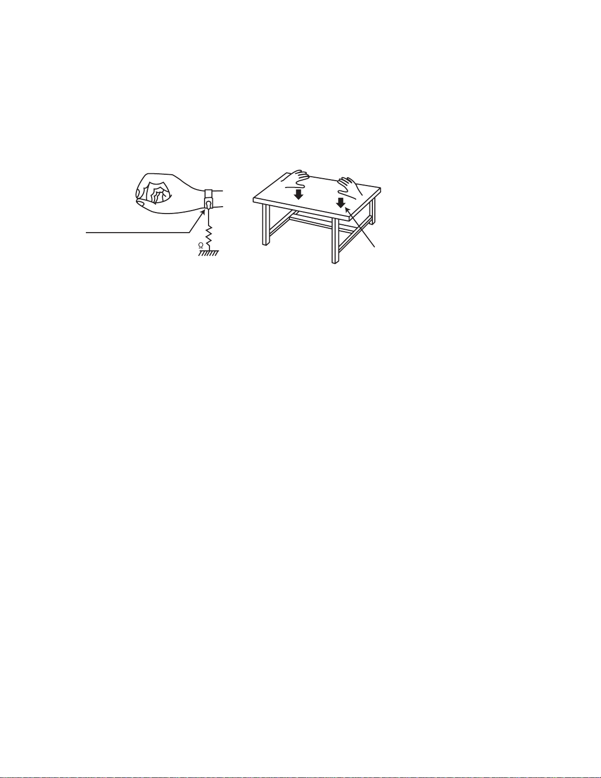
1.5 Preventing static electricity
Electrostatic discharge (ESD), which occurs when static electricity stored in the body, fabric, etc. is discharged, can destroy the laser
diode in the traverse unit (optical pickup). Take care to prevent this when performing repairs.
1.5.1 Grounding to prevent damage by static electricity
Static electricity in the work area can destroy the optical pickup (laser dio de) in devices such as CD players.
Be careful to use proper grounding in the area where repairs are being performed.
(1) Ground the workbench
Ground the workbench by laying conductive material (such as a conductive sh eet) or an iron plate over it before placing the
traverse unit (optical pickup) on it.
(2) Ground yourself
Use an anti-static wrist strap to release any static electricity built up in your body.
(caption)
Anti-static wrist strap
1M
Conductive material
(conductive sheet) or iron palate
(3) Handling the optical pickup
• In order to maintain quality during transport an d before installation, bo th sides of the laser diode on the re placement optical
pickup are shorted. After replacement, return the shorted parts to their original condition.
(Refer to the text.)
• Do not use a tester to check the condition of the laser diode in the optical pickup. The tester's internal power source can easily
destroy the laser diode.
1.6 Handling the traverse unit (optical pickup)
(1) Do not subject the traverse unit (optical pickup) to strong shocks, as it is a sensitive, complex unit.
(2) Cut off the shorted part of the flexible cable using nippers, etc. after replacing the optical pickup. For specific details, refer to the
replacement procedure in the text. Remove the anti-static pin when replacing the traverse unit. Be careful not to take too long
a time when attaching it to the connector.
(3) Handle the flexible cable carefully as it may break when subjected to strong force.
(4) I t is not possible to adjust the semi-fixed resistor that adjusts the laser power. Do not turn it.
1.7 Attention when traverse unit is decomposed
*Please refer to "Disassembly method" in the text for the CD pickup unit.
• Apply solder to the short land sections before the fle xible wire is disconnected from the connector on the CD servo board. (If the
flexible wire is disconnected without applying solder, the CD pickup may be destroyed by static electricity.)
• In the assembly, be sure to remove solder from the short land sections after connecting the flexible wire.
1-4 (No.MB066)
Page 5

SECTION 2
SPECIFIC SERVICE INSTRUCTIONS
This service manual does not describe SPECIFIC SERVICE INSTRUCTIONS.
(No.MB066)1-5
Page 6
SECTION 3
DISASSEMBLY
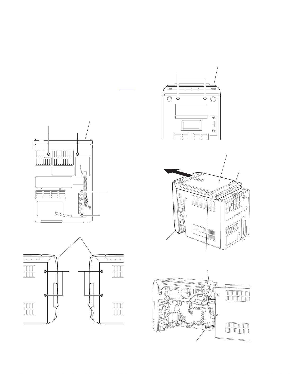
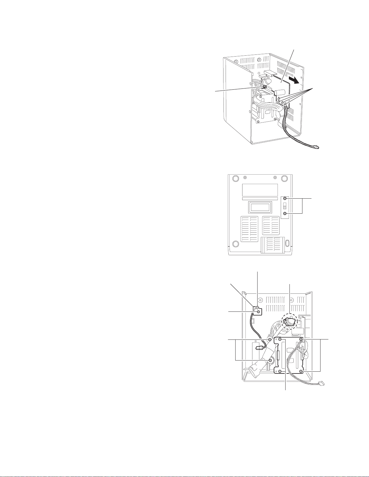
3.1 Main body
3.1.1 Removing the Front panel assembly
(See Fig.1 ~ 5)
(1) Remove the two screws A and the two screws B on the
back of the body.
(2) Remove the four screws C on each side of the body.
(3) Remove the two screws D on the bottom of the body.
(4) Move the front panel assembly in the direction of the arrow
and detach. Disconnect the wire from connector CN860
and FM-ANT.
Caution:
When reassembling, set the tab “a” on the right and left side to
the groove, and move.
CD mechanism assembly
A
Front panel assembly
D
Fig.3
CD mechanism assembly
Fig.1
Front panel assembly
C
Joint a
B
Front panel
assembly
Joint a
Fig.4
FM-ANT
1-6 (No.MB066)
Fig.2
CN860
Fig.5
Page 7
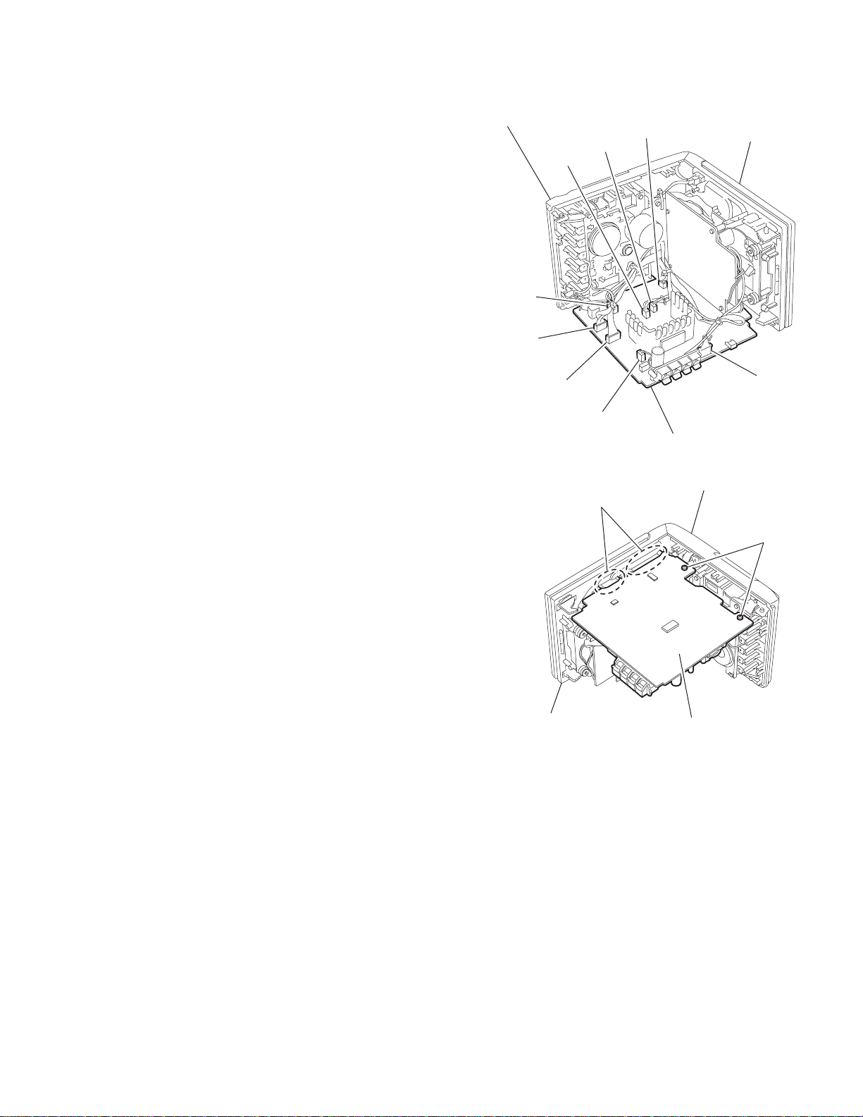
3.1.2 Removing the Main board
(See Fig.6 , 7)
• Prior to performing the fol lowing procedure, remove the front
panel assembly.
(1) Disconnect the wire from all connectors on the main board.
(2) Remove the two screws E and release the joint b.
Front panel
assembly
CN301
CN370
CN601
CN602
CN260
CD mechanism
assembly
CN850
CN851
Joint b
CD mechanism
assembly
CN801
Main board
Fig.6
Front panel assembly
E
Main board
Fig.7
(No.MB066)1-7
Page 8
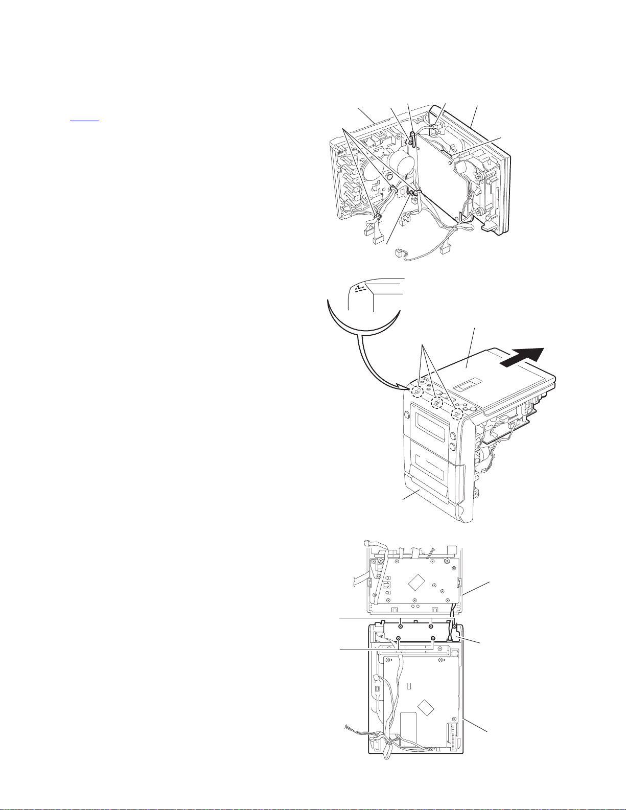
3.1.3 Removing the CD mechanism assembly and the Switch board
(See Fig.8 ~ 10)
• Prior to performing th e following procedure, remove the front
panel assembly and the main board.
(1) Cut off the four bands setting the wires.
(2) Disconnect the wire from connector on the CD open switch
and CN705
(3) Remove the two screws F on the front panel assembly.
(4) Release the joint d of the CD mechanism assembly.
(5) Remove the five screws G attaching the switch board to the
CD mechanism assembly.
on the CD mechanism board.
Front panel
assembly
Band
F
F
Band
Joint d
Open switch
connecter
Fig.8
CD mechanism
assembly
CD mechanism
assembly
CN705
1-8 (No.MB066)
Front panel assembly
G
G
Fig.9
Fig.10
Front panel
assembly
Switch board
CD mechanism
assembly
Page 9
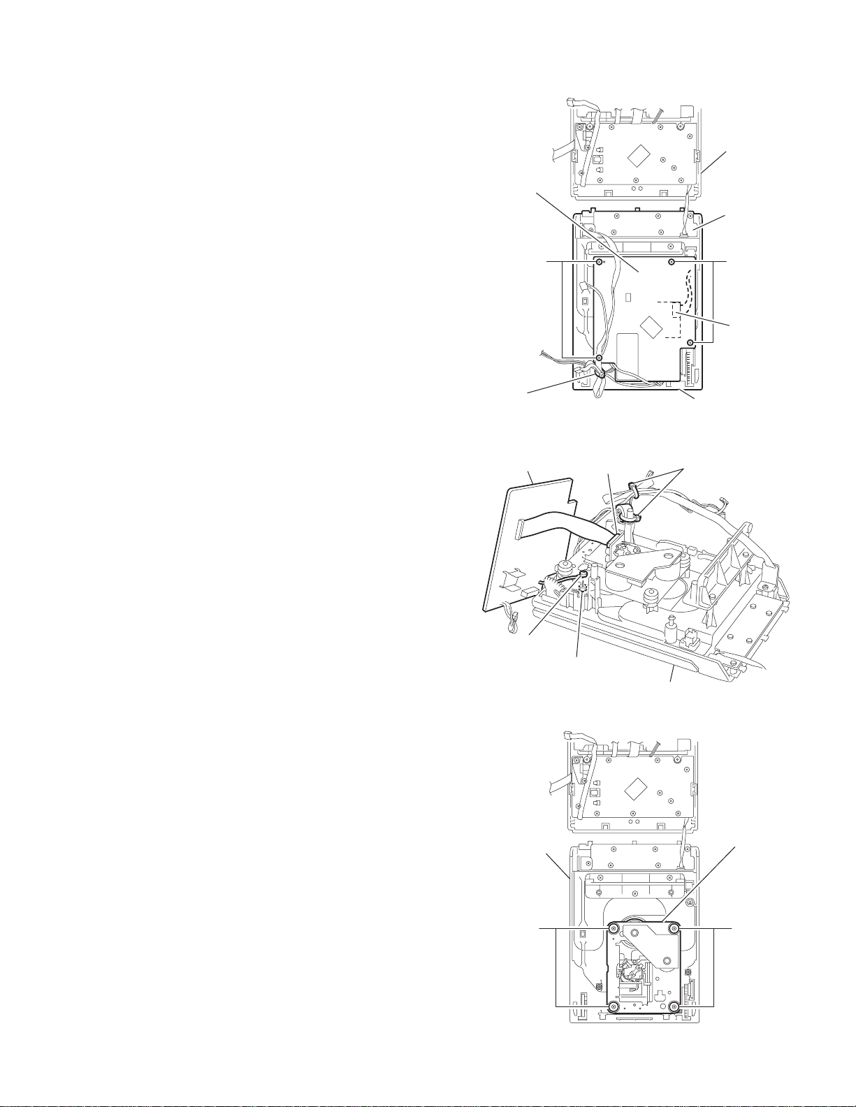
3.1.4 Removing the CD mechanism board
(See Fig.11 ~ 13)
• Prior to performing the fol lowing procedure, remove the front
panel assembly, the main board and the CD mechanism
assembly.
(1) Disconnect connector on the CD mechanism.
(2) Remove the four screws H on the CD mechanism
assembly.
(3) Cut off the band setting each wire and disconnect the card
wire from connector on the CD mechanism.
(4) Remove the screw J attaching the wire on the CD
mechanism board.
Caution:
The metal washer and nut come off.
(5) Remove the four screws K attaching the CD mechanism.
Front panel
CD mechanism
board
Switch board
HH
Connecter
Band
CD mechanism
board
J
Connecter
Nut
Fig.11
Band
CD mechanism
assembly
Fig.12
CD mechanism
assembly
CD mechanism
assembly
KK
CD mechanism
Fig.13
(No.MB066)1-9
Page 10
3.1.5 Removing the Headphone board
(See Fig.14)
• Prior to performing th e following procedure, remove the front
panel assembly, the main board and the CD mechanism
assembly.
(1) Remove the screw L on the bracket and pull out the
headphone board.
3.1.6 Removing the LCD board
(See Fig.15)
• Prior to performing th e following procedure, remove the front
panel assembly, the main board and the CD mechanism
assembly.
(1) Remove the ten screws M and the two screws N on the
Front panel assembly.
Head phones board
Head phones
bracket
L
CD mechanism
assembly
Fig.14
Switch board
M
3.1.7 Removing the Cassette mechanism
(See Fig.16)
• Prior to performing th e following procedure, remove the front
panel assembly and the main board.
(1) Remove the four screws P on the front panel assembly and
press the eject button on the front side to remove the
cassette mechanism assembly.
M
M
Front panel
assembly
N
LCD board
Fig.15
1-10 (No.MB066)
PP
Cassette mechanism
assembly.
Fig.16
Page 11
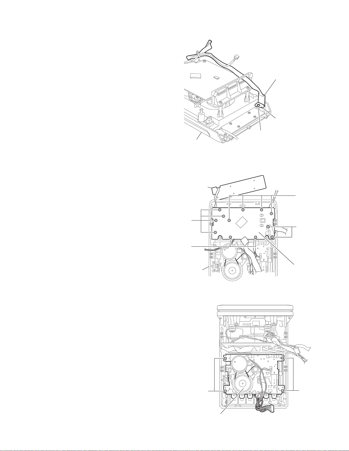
3.1.8 Removing the Transformer board
(See Fig.17)
• Prior to performing the fol lowing procedure, remove the front
panel assembly.
(1) Remove the screw Q on the rear cover assembly.
(2) Pull out the transformer board in the direction of the arrow.
(3) Unsolder the wire extending from the transformer.
3.1.9 Removing the Transformer
(See Fig.18 , 19)
• Prior to performing the fol lowing procedure, remove the front
panel assembly and the transformer board.
(1) Remove the two screws R attaching the voltage selector on
the bottom of the rear cover assembly.
(2) Remove the four screws S on the rear cover assembly.
(3) Remove the two screws T setting the power cord on the
rear cover assembly.
(4) Cut off the band connecting the power cord to the
transformer if necessary, remove the transformer.
Trans borad
Solder point
Q
Fig.17
R
3.1.10 Removing the FM-antenna board
(See Fig.19)
• Prior to performing the fol lowing procedure, remove the front
panel assembly.
(1) Remove the screw U on the rear cover assembly.
(2) Unsolder the FM-antenna wire on the FM-antenna board.
FM ANT board
U
T
Fig.18
Solder point
e Section
S
S
Fig.19
(No.MB066)1-11
Page 12

SECTION 4
ADJUSTMENT
4.1 Measuring instructions required for adjustment
(1) AM signal generator
(2) FM signal generator
(3) Intter mediate frequency sweep generater
(4) FM stereo signal generator
(5) Low-frequency oscillator (oscillation frequency 50 Hz-20
kHz, 0dB output with 600 Ω impeadance)
(6) Attenuator (600 Ω impeadance)
(7) Electric voltmeter
(8) Distotion meter
(9) Torque guage (cassette for CTG-N)
(10) Wow & flutter meter
(11) Frequency counter meter
4.1.1 Amplifier section
Reference output
Speaker output 0 dB(1V)/ 4 Ω
H. Phone output -10 dB(0.1V) 32Ω
4.1.2 CD section
Test disc: JVC standard disc
4.1.3 Test tape
JVC standard test tape
4.1.4 Measuring instruments Radio section
FM 1 kHz, 22.5 kHz deviation
FM STEREO : 1kHz, 67.5 kHz deviation
Pilot signal: 7.5 kHz
AM : 1 kHz, 30% modulation
Reference output:
Speaker output : 0 dB (1V) 4 Ω
Headphone output : -10 dB (0.1V) 32 Ω
1-12 (No.MB066)
Page 13

4.1.5 Cassette Amplifier Section
Head azimuth
adjustment
Tape speed
and wow/
flutter check
and adjustment
PB frequency
response check
Measuring ConditionItem
Test tape:
8 kHz
Signal output
terminal:
PHONES
(with 32 ohm load)
Test tape:
3 kHz
Signal output
terminal:
PHONES
(with 32 ohm load)
Test tape:
Signal output
termnal:
PHONES
(with 32 ohm load)
Check and adjustment procedure
1. Play back the test tape (8 kHz).
2. Adjust the head azimuth adjusting screw so that
the phase difference between the R and L
channels is minimized at an output level that is
within 2 dB of the maximum output level. After
thie adjustment, lock the head azimuth adjusting
screw with screw, sealant to cover more than a
half of the screw head.
3. When the head azimuth is maladjusted, correct it
with the head azimuth adjusting screw.
1. Play back the test tape (3 kHz) by
the end portion.
2. Connect a frequency counter and check that it
reads between 2940 and 3090 Hz. If not, adjust
the frequency with the motor semifixed resistor.
3. Check that the wow/flutter is within 0.38%
(unweighted.)
Play back the test tape while con-firming
that deviation between the 1 kHz signal and 8 kHz
signal should be 0 (+3~-6) dB.
Standard value
Output level:
Within 2 dB of
maximum output
level
Phase difference
L and R
channels:
Minimum
2940 to 3090 Hz
Within 0.38%
(unweighted)
Deviation between
1 kHz and 8 kHz:
0 (+3~-6) dB
Adjusting part
Head azimuth
adjusting
screw (To be
used only
after head
replacement)
See Fig 3-1
Tape
speed:
Motor
semifixed
resister
check only
Bias frequency
check
REC and PB
frequency
response
adjustment
Tape: Normal
Signal output
terminal: Cassette
REC./PLAY HEAD
Test tape:
Signal input FM22.5
DEV 60dB with
Emphasis
signal output
terminal: PHONES
(with 32 ohm load)
Set the TUNER or CD function and with TAPE to
record. Check to see if the frequency at the
measuring point T360 is 60 kHz 1 kHz if not
adjst T360 until the frequency counter indicates
60 kHz 1 kHz.
At TUNER, set the BAND to the FM position, and
record the reference 1 kHz signal and 8kHz signal
alternately repeatedly. While playing back the
recorded signal differ from that of the 1 kHz signal
by within 0 (+3~-6) dB.
T360
Level difference
between REC and
PB: Within 0 (+3~-6)
dB.
(No.MB066)1-13
Page 14

4.1.6 Tuner Section
Item
AM IF adjustment
AM tracking
adjustment
FM Tracking
Adjustment
Measuring
Condition
Signal input:
Loop ANTENNA
Signal output:
U201 PIN 16
Signal input:
Loop antenna
PHONES (with 32
ohm Load)
Signal input point:
FM-ANT
Phones With 32
ohm load
Check and adjustment procedure Standard value Adjusting part
1.Set the intermediate frequency sweep generator to
AM 450 kHz.
2.Adjust the T201 for maximum and center output.
1.Set the TUNER at 531 kHz adjust T202 until the
test pin of R229 Voltage at 1.5V 0.1V.
2.Set the TUNER at 1710 kHz, Check the pin of
R229 Voltage at 8.4V 6V.
3.Set theTUNER and S/G at 603 kHz, adjust T204
for maximum output.
4.Set the TUNER and S/G at 1404 kHz, adjust
VC201 for maximum output.
5.Repeat the above steps 3 and 4.
1.Set the Tuner at 87.5MHz adjust L203 until the test
pin of R230 voltage at 2.4V 0.1V
2.Set the Tuner at 108MHz. Check the pin of R230
voltage at 8 0.8V
3.Set the Tuner and S/G at 90.1MHz. Adjust L204 for
maximum output.
4.Set the Tuner and S/G at 106.1MHz. Adjust VC 202
for maximum output.
5.Repeat the above step 3 and 4
T201
See Fig 3-3
T202
T204
R229
VC201
R230
L204
VC202
1-14 (No.MB066)
Page 15
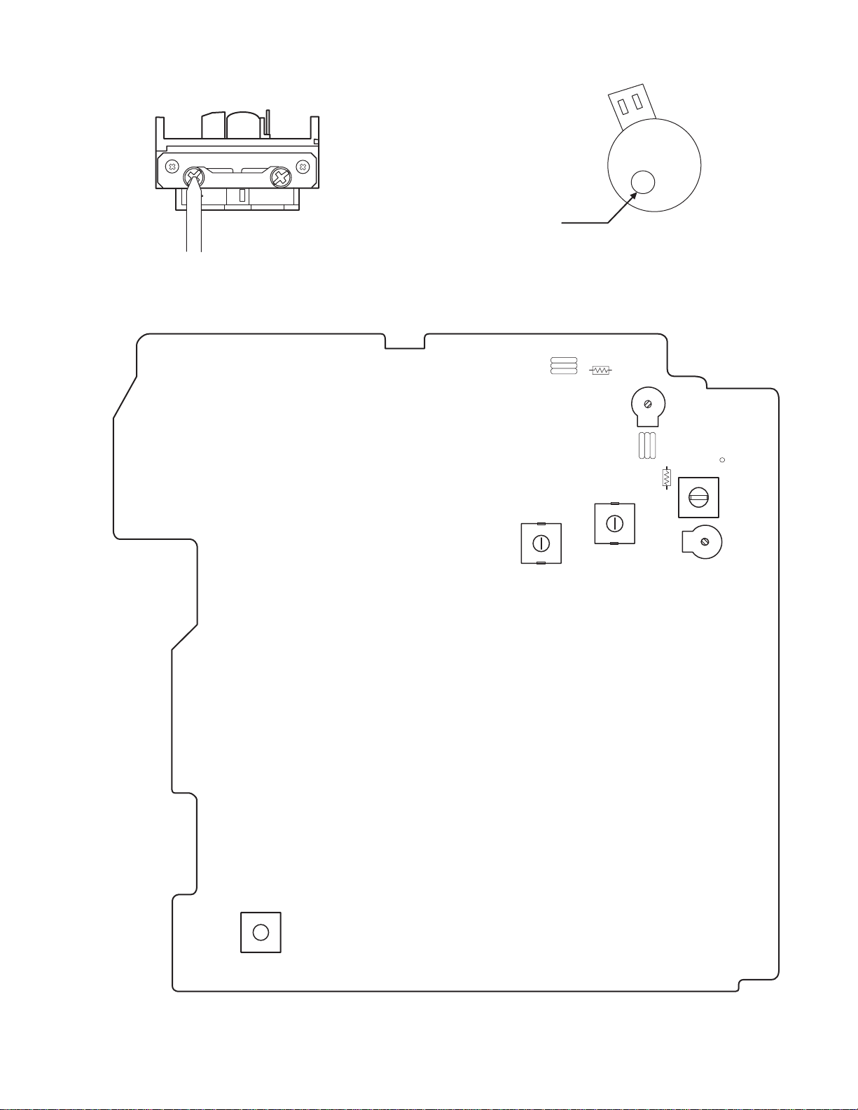
Location of adjusting parts
Cassette mechanism section
Tape Speed Adj.
-
+
CASSETTE MOTOR
Figure 3-1 Head Output Signal
Main board assembly
(AM lF)
(FM OSC)
L203
T201
Figure 3-2
R230
(FM VT)
T202
(AM OSC)
VC202
(FM RF)
L204 (FM RF)
R229
(AM VT)
T202
T204
(AM RF)
FM-ANT
(AM RF)
T360
(BIAS FREQUENCY)
(No.MB066)1-15
Page 16

SECTION 5
TROUBLESHOOTING
Circuit Symptom Cause and Remedy
General No sound
AM
FM
Tape
CD
No sound, weak sound
(Low sensitivity)
No sound, weak sound
(Low sensitivity)
No sound / Recording
Unsteady tape sound,
weak sound
Cannot read the TOC.
no sound
Speakers are not connected:
Check the speaker connection.
Wrong function is selected:
Set switch to the proper position.
Defective volume control:
Set the volume control to a proper sound level.
Defective the Headphone jack:
Replace the headphone jack.
Defect in U801
Check voltages. Replace if necessary.
Defect in U601
Check voltages. Replace if necessary.
Improper location of unit:
Rotate or reposition the unit.
Defect in IF T201:
Check registance, voltage, and current. Replace as needed.
Defect AM antenna coil L202 or oscilloscope coil T202:
Replace if necessary.
Intermediate frequency tuning faulty:
Readjust (see "Adustment").
RF tracking faulty:
Readjust (see "Adjustment").
Defective U201:
Check voltages. Replace if necessary.
Defective U260:
Check voltages. Replace if necessary.
Poor contact in antenna circuit:
Check resistance and resolder.
FM antenna not connected:
Connect the built-in or external antenna.
Defective band selector switch:
Replace or repair the switch.
Defective U201:
Check voltages. Replace if necessary.
Defective U260:
Check voltages. Replace if necessary.
Intermediate frquencytuning faulty:
Readjust (see !Adjustment").
Poor contact in FM antenna circuit:
Resolder or repair as required.
Dirty capstan or head:
Clean the capstan or head with alcohol.
Irreguler cassette tape winding:
Replace tape.
Defective U301:
Check voltage. Replace if necessary.
Cassette erasure prevention tabs broken out:
Replace tape or cover tab openings with adhesive tape.
Disc is inserted upside down:
Insert disc correctry.
Disc is dirty:
Wipe clean with a soft cloth.
Disc is scratched:
Use a new disc.
Disc is seriously warped:
Use a new disc.
A non-standard disc has been inserted:
Use only a barand neme disc.
Moisuture has formed inside the CD deck:
Wait about 20 to 30 minutes.
Defective IC701:
Check voltages. Replace if necessary.
Defective IC702:
Check voltages. Replace if necessary.
Defective IC703:
Check voltages. Replace if necessary.
Defect in the CD pickup mechanism:
Replace as required.
1-16 (No.MB066)
Page 17

(No.MB066)1-17
Page 18

VICTOR COMPANY OF JAPAN, LIMITED
AV & MULTIMEDIA COMPANY AUDIO/VIDEO SYSTEMS CATEGORY 10-1,1chome,Ohwatari-machi,Maebashi-city,371-8543,Japan
(No.MB066)
Printed in Japan
WPC
Page 19

SCHEMATIC DIAGRAMS
MICRO COMPONENT SYSTEM
UX-H10
CD-ROM No.SML200401
TIMER
TIMER SET
STANDBY/ON
ON/OFF
RANDOM SLEEP
INTRO
REMAIN
TUNER
TAPE CD
/BAND
BEAT CUT
DISPLAY
/CLOCK SET
SOUND
MUTING
/BASS
REPEAT
ST/MONOPROGRAM
CD
VOLUME
STANDBY/ON
STANDBY
MICRO COMPONENT SYSTEM
UX-H10
VOLUME
RM-SUXH10U REMOTE CONTROL
CD SYNCHRO RECORDING
OPEN
Area Suffix
US ---------------- Singapore
UT ---------------------Taiwan
UW ---- Brazil,Mexico,Peru
Contents
Block diagram ------------------------------------------------------- 2-1
Standard schematic diagrams ---------------------------------- 2-2
Printed circuit boards --------------------------------------------- 2-9 to 12
COPYRIGHT 2004 VICTOR COMPANY OF JAPAN, LTD.
No.MB066SCH
2004/1
Page 20

In regard with component parts appearing on the silk-screen printed side (parts side) of
the PWB diagrams, the parts that are printed over with black such as the resistor ( ),
diode ( ) and ICP ( ) or identified by the " " mark nearby are critical for safety.
(This regulation does not correspond to J and C version.)
Page 21

Block diagram
2-1
Page 22

Standard schematic diagrams
Power supply section
Parts are safety assurance parts.
When replacing those parts make
sure to use the specified one.
2-2
Page 23

Amp section
Parts are safety assurance parts.
When replacing those parts make
sure to use the specified one.
2-3
Page 24

Display section
2-4
Page 25

Remote section
2-5
Page 26

CD section
Parts are safety assurance parts.
When replacing those parts make
sure to use the specified one.
2-6
Page 27

Cassette section
Parts are safety assurance parts.
When replacing those parts make
sure to use the specified one.
2-7
Page 28

Tuner section
2-8
Page 29

Printed circuit boards
Main board
2-9
Page 30

CD board
2-10
Page 31

Power board (forward side) Display board (forward side)
Display board (reverse side)Power board (reverse side)
2-11
Page 32

FM antenna board
Headphone board LED board
Remocon board (forward side) Key board (forward side)
Key board (reverse side)Remocon board (reverse side)
2-12
Page 33

< MEMO >
Page 34

VICTOR COMPANY OF JAPAN, LIMITED
AV & MULTIMEDIA COMPANY AUDIO/VIDEO SYSTEMS CATEGORY 10-1,1chome,Ohwatari-machi,Maebashi-city,371-8543,Japan
(No.MB066SCH)
Printed in Japan
WPC
Page 35

PARTS LIST
[ UX-H10 ]
* All printed circuit boards and its assemblies are not available as service parts.
Area suffix
US ---------------------- Singapore
UT --------------------------- Taiwan
UW ---------- Brazil,Mexico,Peru
MB066
- Contents -
Exploded view of general assembly and parts list (Block No.M1)
Electrical parts list (Block No.01~05)
Packing materials and accessories parts list (Block No.M3)
3- 2
3- 5
3-12
3-1
Page 36

Exploded view of general assmbly and parts list
Block No.
M
M
1
M
15
60
LED
BOARD
62
63
64
1
a'
a
8
2
3
KEY BOARD
4
5
6
67
A
39
37
B
69
73
e
m
PHONE
BOARD
12
68
r
69
7
g
68
68
11
r
22
72
69
h
68
20
21
72
c
71
22
72
k
49
51
52
50
38
53
56
54
F
47
55
55
58
46
55
45
65
55
E
17
44
59
n
48
43
DISPLAY
BOARD
d
c
42
69
68
41
p
CN704
70
40
CD BOARD
69
q
3-2
Page 37

M
M
g
68
r
68
DISPLAY
BOARD
p
68
CN704
22
7
11
70
72
h
15
71
69
k
CD BOARD
69
75
h
FM ANT
BOARD
f
73
g
j
28
76
27
74
16
19
13
71
H
14
b
70
17
A
70
80
81
21
72
82
79
74
26
a'
a
20
21
18
72
c
22
72
d
b
70
35
e
B
34
75
78
F
E
q
H
f
D
33
MAIN
BOARD
n
k
m
p
69
30
68
40
q
69
70
31
69
74
G
24
F901
F902
77
29
70
POWER BOARD
j
G
32
D
76
3-3
Page 38

General assembly
Block No. [M][1][M][M]
Symbol No.
1 OW43-00010-00 CD DOOR LENS PMMA
2 OW66-00010-03 CD DOOR ABS
3 OW39-04200-00 METAL COVER
4 OW97-09019-00 P.C.MAGNET 20495830
5 OW49-04200-00 STABILIZER RING
6 OW55-09019-01B PLASTIC COVER W/O Felt
7 OW48-00010-05 CD TRAY HIPS
8 OW53-00010-00 FUNCTION KNOB ABS
11 OW39-00010-00 PHONE PCB BKT BKT.
12 OW48-04200-01 CD BKT. ABS
13 OW55-00141-02 PUSH ROD NSX01-050
14 OW36-00003-04 CD EJECT SPRING
15 OW16-10101-92L CD DOOR SWITCH DLS-02-1
16 OW36-03232-02 CD DOOR SPRING
17 OW63-00303-01 DAMPER Gear B40GG(x2)
18 OW48-07930-08 CD MECHA COVER Thomson CD
19 OW98-04200-00 CD MECHA Thomson TCP11TK
20 OW35-00003-00 E RING M3
21 OW81-02750-00 CD DAMPER
22 OW81-02750-01 CD DAMPER
24 OW48-00010-01 POWER PCB BKT BKT.
26 OW35-10019-00 FIBRE WASHER F14 X F3 X 1.5mm
27 OW61-00010-03 REAR CABINET
28 OW30-00020-01S AC POWER CORD
28 OW30-00010-06 AC POWER CORD UT
29 OW81-04200-00 RUBBER FOOT
30 OW81-00010-00 RUBBER FOOT 13X6mm
31 OW49-00010-00 AC CORD HOLDER ABS
32 OW15-00010-05 TRANS FORMER
33 TA8229K IC OW03-08229-00
34 KTD2058 TRANSISTOR OW01-02058-00
35 OW39-04200-02 HEAT SINK
37 OW48-00010-03 MAIN PCB BKT2
38 OW36-00010-00 CASS KNOB Door Plate
39 OW48-00010-02 MAIN PCB BKT1
40 OW39-04200-04 CASS KNOB BKT
41 OW53-00010-06 CASS KNOB Pause
42 OW53-00010-08 CASS KNOB Stop/Eject
43 OW53-00010-04 CASS KNOB F.FWD
44 OW53-00010-05 CASS KNOB REW.
45 OW53-00010-03 CASS KNOB Play
46 OW53-00010-07 CASS KNOB REC.
47 OW66-00010-02 CASS KNOB Door
48 OW36-00010-01 CASS DOOR SPRIN Spring
49 OW43-00010-01 CASS DOOR LENS Lens
50 OW66-00010-01 CASS DOOR ABS
51 OW48-04200-04 CASS DOOR BKT BKT.
52 OW43-00010-03 DISPLAY LENS PMMA
53 OW55-30000-00 JVC BADGE ABS
54 OW60-00010-01 FRONT CABINET HB
55 OW39-04200-05 PANEL FIXING Plate(x6)
56 OW53-00010-01 POWER KNOB ABS
58 OW53-00010-02 VOLUME KNOB ABS
59 OW94-04200-00 CASS DECK CS-2SC-3222
60 OW91-80010-00 LCD
62 OW43-00010-04 LCD FILTER
63 OW43-00010-02 LIGHT GUIDE PMMA
64 OW68-00010-00 LIGHT GUIDE Paper 0.15TH
65 OW48-00010-00 LCD BKT BKT.
67 OW40-02045-90 SCREW F 2.0 X 4.5
68 OW40-12608-01 SCREW F 2.6 X 8(x18)
69 OW40-13010-01 SCREW F 3.0 X 10(x14)
70 OW40-13008-01 SCREW F 3.0 X 8(x8)
71 OW40-02005-90 SCREW F2.0 X 5(x3)
72 OW40-52610-03 SCREW F2.6 X 10(x4)
73 OW40-12606-01 SCREW F2.6 X 12(x3)
74 OW40-03006-22 SCREW M3 X 6(x6)
75 OW40-13008-41 SCREW F3.0 X 8(x2)
76 OW40-13012-01 SCREW F3.0 X12(x6)
77 OW40-03010-02 SCREW M3 X 10(x2)
78 OW16-10212-00 VOLTAGE SW.
Part No. Part Name Description Local
3140-114-13892(x2)
3140-114-13902(x2)
F11X3mm W/
Tape(x2)
US
UW
Symbol No.
79 OW40-03005-01 SCREW M3 X 5
80 OW35-40007-00 STEEL NUT M3
81 OW35-20001-04 TOOTH WASHER M3
82 OW35-30005-00 SOLDERING LUG F3.5mm L=9mm
Part No. Part Name Description Local
3-4
Page 39

Electrical parts list
Main board
Block No. [0][1][0][0]
Symbol No.
Q204 9014 TRANSISTOR OW01-09014-05 S
Q205 9014 TRANSISTOR OW01-09014-05 S
Q206 9014 TRANSISTOR OW01-09014-05 S
Q207 9014 TRANSISTOR OW01-09014-05 S
Q209 9014 TRANSISTOR OW01-09014-05 S
Q210 9014 TRANSISTOR OW01-09014-05 S
Q260 9014 TRANSISTOR OW01-09014-05 S
Q261 9014 TRANSISTOR OW01-09014-05 S
Q262 9014 TRANSISTOR OW01-09014-05 S
Q263 9014 TRANSISTOR OW01-09014-05 S
Q280 9014 TRANSISTOR OW01-09014-05 S
Q281 8550 TRANSISTOR OW01-08550-06 S
Q300 8050 TRANSISTOR OW01-08050-06 S
Q301 2SC2412 TRANSISTOR OW01-02412-00R
Q302 2SC2412 TRANSISTOR OW01-02412-00R
Q303 2SC2412 TRANSISTOR OW01-02412-00R
Q304 2SC2412 TRANSISTOR OW01-02412-00R
Q305 2SC2412 TRANSISTOR OW01-02412-00R
Q306 2SC2412 TRANSISTOR OW01-02412-00R
Q307 8050 TRANSISTOR OW01-08050-06 S
Q308 8050 TRANSISTOR OW01-08050-06 S
Q309 9014 TRANSISTOR OW01-09014-05 S
Q310 9014 TRANSISTOR OW01-09014-05 S
Q311 9014 TRANSISTOR OW01-09014-05 S
Q312 9014 TRANSISTOR OW01-09014-05 S
Q313 9014 TRANSISTOR OW01-09014-05 S
Q314 9014 TRANSISTOR OW01-09014-05 S
Q315 9014 TRANSISTOR OW01-09014-05 S
Q316 9014 TRANSISTOR OW01-09014-05 S
Q317 8550 TRANSISTOR OW01-08550-06 S
Q318 8550 TRANSISTOR OW01-08550-06 S
Q319 9014 TRANSISTOR OW01-09014-05 S
Q360 8050 TRANSISTOR OW01-08050-06 S
Q361 2SC2412 TRANSISTOR OW01-02412-00R
Q370 8550 TRANSISTOR OW01-08550-06 S
Q803 9014 TRANSISTOR OW01-09014-05 S
Q804 9014 TRANSISTOR OW01-09014-05 S
Q830 KTD2058Y TRANSISTOR OW01-02058-00 K
Q831 8550 TRANSISTOR OW01-08550-06 S
Q832 9014 TRANSISTOR OW01-09014-05 S
Q850 2SB926T-AA TRANSISTOR OW01-00926-01
Q851 9014 TRANSISTOR OW01-09014-05 S
Q860 2SC945P TRANSISTOR OW01-00945-16 N
Q861 2SC1383R TRANSISTOR OW01-01383-19
D201 1SS-133TP FR DIODE OW02-00133-00 R
D202 1SS-133TP FR DIODE OW02-00133-00 R
D203 1SS-133TP FR DIODE OW02-00133-00 R
D204 1SS-133TP FR DIODE OW02-00133-00 R
D205 1SS-133TP FR DIODE OW02-00133-00 R
D221 1SS-133TP FR DIODE OW02-00133-00 R
D301 1SS-133TP FR DIODE OW02-00133-00 R
D302 1SS-133TP FR DIODE OW02-00133-00 R
D303 1SS-133TP FR DIODE OW02-00133-00 R
D304 1SS-133TP FR DIODE OW02-00133-00 R
D306 1SS-133TP FR DIODE OW02-00133-00 R
D307 1SS-133TP FR DIODE OW02-00133-00 R
D370 1N4001 FR DIODE OW02-04001-00
D801 1SS-133TP FR DIODE OW02-00133-00 R
D850 1SS-133TP FR DIODE OW02-00133-00 R
D851 1SS-133TP FR DIODE OW02-00133-00 R
D862 1SS-133TP FR DIODE OW02-00133-00 R
D863 1SS-133TP FR DIODE OW02-00133-00 R
C200 OW05-00220-06 C CAPACITOR 22PF NPO
C201 OW05-00220-06 C CAPACITOR 22PF NPO
C203 OW06-50474-20 E CAPACITOR 0.47MF 50V PITC
C204 OW05-03102-06T C CAPACITOR 1000PF
C205 OW05-00102-82 C CAPACITOR 0.001MF +80-20%
C206 OW05-00030-06 C CAPACITOR 3PF NPO
C207 OW06-50475-02 E CAPACITOR 4.7MF 50V PITCH
C209 OW05-02103-10 M CAPACITOR 0.01MF
Part No. Part Name Description Local
Symbol No.
C210 OW05-02103-10 M CAPACITOR 0.01MF
C211 OW06-50475-02 E CAPACITOR 4.7MF 50V PITCH
C212 OW06-50475-02 E CAPACITOR 4.7MF 50V PITCH
C214 OW05-03223-06T C CAPACITOR 0.022MF
C215 OW05-02202-10 M CAPACITOR 0.002MF
C216 OW05-02202-10 M CAPACITOR 0.002MF
C217 OW05-03223-06T C CAPACITOR 0.022MF
C219 OW06-50104-03 E CAPACITOR 0.1MF 50V
C220 OW06-50105-02 E CAPACITOR 1MF 50V PITCH=5
C221 OW06-50104-03 E CAPACITOR 0.1MF 50V
C222 OW06-50475-02 E CAPACITOR 4.7MF 50V PITCH
C223 OW05-03331-03T CHIP CAPACITOR 330PF
C224 OW05-07223-82A C CAPACITOR 0.022MF
C225 OW05-03103-06T C CAPACITOR 0.01MF B500 K10
C226 OW05-03200-03T C CAPACITOR 20PF N500 J200
C227 OW05-03473-06T C CAPACITOR 0.047MF B500 K4
C229 OW05-00473-82 C CAPACITOR 0.047MF
C230 OW05-00180-06 C CAPACITOR 18PF NPO
C231 OW05-00102-82 C CAPACITOR 0.001MF +80/-20
C232 OW05-03080-03T C CAPACITOR 8PF
C233 OW05-03102-06T C CAPACITOR 1000PF B500 K10
C234 OW05-03103-06T C CAPACITOR 0.01MF B500 K10
C235 OW05-03102-06T C CAPACITOR 1000PF B500 K10
C236 OW06-16227-02 E CAPACITOR 220MF 16V PITCH
C237 OW05-03330-03T CHIP CAPACITOR 33PF N500 J330
C238 OW05-09391-05 P CAPACITOR 390PF
C239 OW05-03473-06T C CAPACITOR 0.047MF B500 K4
C240 OW06-16226-02 E CAPACITOR 22MF 16V PITCH=
C244 OW05-00120-06 C CAPACITOR 12PF NPO
C245 OW05-00102-82 C CAPACITOR 0.001MF +80/-20
C247 OW05-03222-06T C CAPACITOR 2200PF B500 K22
C248 OW05-03222-06T C CAPACITOR 2200PF B500 K22
C260 OW05-03330-03T CHIP CAPACITOR 33PF N500 J330
C261 OW05-03330-03T CHIP CAPACITOR 33PF N500 J330
C262 OW05-03223-06T C CAPACITOR 0.022MF B500 K2
C263 OW06-16107-02 E CAPACITOR 100MF 16V
C264 OW05-03103-06T C CAPACITOR 0.01MF B500 K10
C265 OW05-03102-06T C CAPACITOR 1000PF B500 K10
C266 OW06-50335-02 E CAPACITOR 3.3MF 50V PITCH
C267 OW05-03223-06T C CAPACITOR 0.022MF B500 K2
C269 OW06-50105-02 E CAPACITOR 1MF 50V PITCH=5
C270 OW05-03223-06T C CAPACITOR 0.022MF B500 K2
C272 OW06-25477-02 E CAPACITOR 470MF 25V PITCH
C273 OW05-07104-82B C CAPACITOR 0.1MF 50V
C274 OW05-03101-06T C CAPACITOR 100PF N101J 500
C284 OW05-03104-06T C CAPACITOR 0.1MF
C285 OW05-03221-03T CHIP CAPACITOR 220PF N500 J221
C286 OW05-03221-03T CHIP CAPACITOR 220PF N500 J221
C287 OW05-03221-03T CHIP CAPACITOR 220PF N500 J221
C292 OW05-03104-06T C CAPACITOR 0.1MF
C293 OW05-07102-10A C CAPACITOR 1000PF
C294 OW05-03223-06T C CAPACITOR 0.022MF B500 K2
C301 OW05-03102-06T C CAPACITOR 1000PF B500 K10
C302 OW05-03102-06T C CAPACITOR 1000PF B500 K10
C303 OW06-16227-02 E CAPACITOR 220MF 16V PITCH
C304 OW06-16227-02 E CAPACITOR 220MF 16V PITCH
C307 OW05-03331-03T CHIP CAPACITOR 330PF N500 J331
C308 OW05-03331-03T CHIP CAPACITOR 330PF N500 J331
C309 OW06-50475-02 E CAPACITOR 4.7MF 50V PITCH
C310 OW06-50475-02 E CAPACITOR 4.7MF 50V PITCH
C311 OW05-03272-06T C CAPACITOR 0.002MF B500 K2
C312 OW05-03272-06T C CAPACITOR 0.0027MF
C315 OW05-02333-10 M CAPACITOR 0.033MF
C316 OW05-02333-10 M CAPACITOR 0.033MF
C317 OW05-02333-10 M CAPACITOR 0.033MF
C318 OW05-02333-10 M CAPACITOR 0.033MF
C319 OW06-50104-03 E CAPACITOR 0.1MF 50V
C320 OW06-50104-03 E CAPACITOR 0.1MF 50V
C321 OW05-03152-06T C CAPACITOR 1500PF B500 K15
C322 OW05-03152-06T C CAPACITOR 1500PF B500 K15
C323 OW06-50105-02 E CAPACITOR 1MF 50V PITCH=5
C324 OW06-25106-02 E CAPACITOR 10MF 25V PITCH=
C325 OW06-16227-02 E CAPACITOR 220MF 16V PITCH
C326 OW05-03223-06T C CAPACITOR 0.022MF B500 K2
C327 OW05-03182-06T C CAPACITOR 0.0018MF B500 K
C328 OW05-03182-06T C CAPACITOR 0.0018MF B500 K
Part No. Part Name Description Local
3-5
Page 40

Symbol No.
Part No. Part Name Description Local
Symbol No.
Part No. Part Name Description Local
C329 OW06-50105-02 E CAPACITOR 1MF 50V PITCH=5
C330 OW06-50105-02 E CAPACITOR 1MF 50V PITCH=5
C331 OW06-50105-02 E CAPACITOR 1MF 50V PITCH=5
C332 OW06-50105-02 E CAPACITOR 1MF 50V PITCH=5
C333 OW05-02102-10 M CAPACITOR 0.001MF
C334 OW05-02102-10 M CAPACITOR 0.001MF
C335 OW05-03151-03T C CAPACITOR 150PF N151J 500
C336 OW05-03151-03T C CAPACITOR 150PF N151J 500
C337 OW05-03151-03T C CAPACITOR 150PF N151J 500
C338 OW05-03151-03T C CAPACITOR 150PF N151J 500
C339 OW06-16227-02 E CAPACITOR 220MF 16V PITCH
C340 OW06-25106-02 E CAPACITOR 10MF 25V PITCH=
C341 OW06-16476-02 E CAPACITOR 47MF 16V
C342 OW06-25106-02 E CAPACITOR 10MF 25V PITCH=
C343 OW06-16107-02 E CAPACITOR 100MF 16V
C344 OW05-03223-06T C CAPACITOR 0.022MF B500 K2
C345 OW06-16475-02 E CAPACITOR 4.7MF 16V
C360 OW05-02392-10 M CAPACITOR 0.0039MF
C361 OW05-03331-03T CHIP CAPACITOR 330PF N500 J331
C362 OW05-02103-10 M CAPACITOR 0.01MF
C363 OW05-02102-10 M CAPACITOR 0.001MF
C364 OW05-02102-10 M CAPACITOR 0.001MF
C365 OW06-16336-02 E CAPACITOR 33MF 16V PITCH=
C366 OW05-03223-06T C CAPACITOR 0.022MF B500 K2
C367 OW05-03223-06T C CAPACITOR 0.022MF B500 K2
C370 OW05-03223-06T C CAPACITOR 0.022MF B500 K2
C371 OW05-03223-06T C CAPACITOR 0.022MF B500 K2
C372 OW05-03223-06T C CAPACITOR 0.022MF B500 K2
C373 OW06-16227-02 E CAPACITOR 220MF 16V PITCH
C374 OW05-07223-82A C CAPACITOR 0.022MF
C601 OW06-50475-02 E CAPACITOR 4.7MF 50V PITCH
C602 OW06-50475-02 E CAPACITOR 4.7MF 50V PITCH
C603 OW06-50475-02 E CAPACITOR 4.7MF 50V PITCH
C604 OW06-50475-02 E CAPACITOR 4.7MF 50V PITCH
C605 OW06-50475-02 E CAPACITOR 4.7MF 50V PITCH
C606 OW06-50475-02 E CAPACITOR 4.7MF 50V PITCH
C607 OW06-50475-02 E CAPACITOR 4.7MF 50V PITCH
C608 OW06-50475-02 E CAPACITOR 4.7MF 50V PITCH
C611 OW06-50475-02 E CAPACITOR 4.7MF 50V PITCH
C612 OW06-50475-02 E CAPACITOR 4.7MF 50V PITCH
C615 OW05-02104-10 M CAPACITOR 0.1MF
C616 OW05-02104-10 M CAPACITOR 0.1MF
C617 OW06-50105-02 E CAPACITOR 1MF 50V PITCH=5
C618 OW06-50105-02 E CAPACITOR 1MF 50V PITCH=5
C619 OW06-50475-02 E CAPACITOR 4.7MF 50V PITCH
C620 OW06-50475-02 E CAPACITOR 4.7MF 50V PITCH
C621 OW05-02103-10 M CAPACITOR 0.01MF
C622 OW05-02103-10 M CAPACITOR 0.01MF
C623 OW06-16227-02 E CAPACITOR 220MF 16V PITCH
C624 OW05-03104-06T C CAPACITOR 0.1MF
C625 OW06-16107-02 E CAPACITOR 100MF 16V
C626 OW05-07223-82A C CAPACITOR 0.022MF
C628 OW05-03221-03T CHIP CAPACITOR 220PF N500 J221
C629 OW05-03221-03T CHIP CAPACITOR 220PF N500 J221
C630 OW05-03103-06T C CAPACITOR 0.01MF B500 K10
C631 OW05-03103-06T C CAPACITOR 0.01MF B500 K10
C801 OW06-16226-02 E CAPACITOR 22MF 16V PITCH=
C802 OW05-03102-06T C CAPACITOR 1000PF B500 K10
C803 OW05-03102-06T C CAPACITOR 1000PF B500 K10
C807 OW06-50225-02 E CAPACITOR 2.2MF 50V
C808 OW06-50225-02 E CAPACITOR 2.2MF 50V
C809 OW06-16476-02 E CAPACITOR 47MF 16V
C810 OW06-16476-02 E CAPACITOR 47MF 16V
C811 OW06-16108-00 E CAPACITOR 1000MF 16V
C812 OW06-16108-00 E CAPACITOR 1000MF 16V
C813 OW06-16107-02 E CAPACITOR 100MF 16V
C814 OW06-16107-02 E CAPACITOR 100MF 16V
C815 OW05-02154-10 M CAPACITOR 0.15MF
C816 OW05-02154-10 M CAPACITOR 0.15MF
C817 OW05-03104-06T C CAPACITOR 0.1MF
C818 OW06-16227-02 E CAPACITOR 220MF 16V PITCH
C819 OW06-25338-00 E CAPACITOR 3300MF 25V
C820 OW06-25477-02 E CAPACITOR 470MF 25V
C823 OW05-07104-82B C CAPACITOR 0.1MF 50V
C825 OW05-03104-06T C CAPACITOR 0.1MF
C826 OW05-03104-06T C CAPACITOR 0.1MF
C830 OW05-03104-06T C CAPACITOR 0.1MF
C831 OW06-16107-02 E CAPACITOR 100MF 16V
C832 OW05-03104-06T C CAPACITOR 0.1MF
C833 OW05-03104-06T C CAPACITOR 0.1MF
C851 OW05-00104-82 C CAPACITOR 0.1MF +80%-20%
C852 OW06-25108-00 E CAPACITOR 1000MF 25V
C853 OW05-03104-06T C CAPACITOR 0.1MF
C860 OW06-25106-02 E CAPACITOR 10MF 25V PITCH=
C861 OW06-25106-02 E CAPACITOR 10MF 25V PITCH=
C862 OW06-16107-02 E CAPACITOR 100MF 16V
C863 OW06-16227-02 E CAPACITOR 220MF 16V PITCH
VC201 OW05-08200-03 TR CAPACITOR 20PF 3PIN
VC202 OW05-08100-03 TR CAPACITOR 10PF 3PIN
R146 OW07-15121-50T C RESISTOR 120 1/8W 52MM T
R147 OW07-15121-50T C RESISTOR 120 1/8W 52MM T
R200 OW07-25274-60K C RESISTOR 270K RMC 1/16
R201 OW07-25331-60K C RESISTOR 330 1/8W
R202 OW07-25103-60K C RESISTOR 10K RMC 1/16 10
R203 OW07-15473-50T C RESISTOR 47K 1/8W 52MM T
R207 OW07-25103-60K C RESISTOR 10K RMC 1/16 10
R209 OW07-15100-50T C RESISTOR 10 1/8W 52MM T.
R211 OW07-25123-60K C RESISTOR 12K RMC 1/16 12
R212 OW07-25123-60K C RESISTOR 12K RMC 1/16 12
R213 OW07-25392-60K C RESISTOR 3.9K RMC 1/16
R214 OW07-25392-60K C RESISTOR 3.9K RMC 1/16
R215 OW07-25473-60K C RESISTOR 47K RMC 1/16 47
R216 OW07-25102-60K C RESISTOR 1K RMC 1/16 102
R218 OW07-25473-60K C RESISTOR 47K RMC 1/16 47
R222 OW07-25332-60K C RESISTOR 3.3K RMC 1/16
R223 OW07-25332-60K C RESISTOR 3.3K RMC 1/16
R225 OW07-15102-50T C RESISTOR 1K 1/8W 52MM T.
R226 OW07-25104-60K C RESISTOR 100K RMC 1/16
R227 OW07-25222-60K C RESISTOR 2.2K RMC 1/16
R228 OW07-15220-50T C RESISTOR 22 1/8W 52MM T.
R229 OW07-15103-50T C RESISTOR 10K 1/8W 52MM T
R230 OW07-15473-50T C RESISTOR 47K 1/8W 52MM T
R232 OW07-15221-50T C RESISTOR 220 1/8W 52MM T
R233 OW07-15101-50T C RESISTOR 100 1/8W 52MM T
R235 OW07-25103-60K C RESISTOR 10K RMC 1/16 10
R236 OW07-25103-60K C RESISTOR 10K RMC 1/16 10
R238 OW07-25103-60K C RESISTOR 10K RMC 1/16 10
R239 OW07-25103-60K C RESISTOR 10K RMC 1/16 10
R242 OW07-25223-60K C RESISTOR 22K RMC 1/16 22
R247 OW07-25822-60K C RESISTOR 8.2K RMC 1/16
R248 OW07-25822-60K C RESISTOR 8.2K RMC 1/16
R260 OW07-25000-60K C RESISTOR 0 RMC 1/16 000J
R261 OW07-25102-60K C RESISTOR 1K RMC 1/16 102
R262 OW07-25102-60K C RESISTOR 1K RMC 1/16 102
R263 OW07-25102-60K C RESISTOR 1K RMC 1/16 102
R265 OW07-25102-60K C RESISTOR 1K RMC 1/16 102
R266 OW07-25102-60K C RESISTOR 1K RMC 1/16 102
R267 OW07-25561-60K C RESISTOR 560 1/16 561JTP
R268 OW07-25152-60K C RESISTOR 1.5K RMC 1/16
R269 OW07-25152-60K C RESISTOR 1.5K RMC 1/16
R270 OW07-25102-60K C RESISTOR 1K RMC 1/16 102
R271 OW07-25472-60K C RESISTOR 4.7K RMC 1/16
R272 OW07-25472-60K C RESISTOR 4.7K RMC 1/16
R273 OW07-15221-50T C RESISTOR 220 1/8W 52MM T
R274 OW07-25103-60K C RESISTOR 10K RMC 1/16 10
R275 OW07-25103-60K C RESISTOR 10K RMC 1/16 10
R276 OW07-25103-60K C RESISTOR 10K RMC 1/16 10
R277 OW07-25102-60K C RESISTOR 1K RMC 1/16 102
R278 OW07-25102-60K C RESISTOR 1K RMC 1/16 102
R279 OW07-15103-50T C RESISTOR 10K 1/8W 52MM T
R280 OW07-25103-60K C RESISTOR 10K RMC 1/16 10
R281 OW07-15103-50T C RESISTOR 10K 1/8W 52MM T
R282 OW07-25182-60K C RESISTOR 1.8K RMC 1/16
R284 OW07-15102-50T C RESISTOR 1K 1/8W 52MM T.
R285 OW07-15102-50T C RESISTOR 1K 1/8W 52MM T.
R286 OW07-25104-60K C RESISTOR 100K RMC 1/16
R290 OW07-25103-60K C RESISTOR 10K RMC 1/16 10
R293 OW07-25274-60K C RESISTOR 270K RMC 1/16
R294 OW07-25224-60K C RESISTOR 220K RMC 1/16
R301 OW07-25102-60K C RESISTOR 1K RMC 1/16 102
R302 OW07-25102-60K C RESISTOR 1K RMC 1/16 102
R303 OW07-25332-60K C RESISTOR 3.3K RMC 1/16
R304 OW07-25332-60K C RESISTOR 3.3K RMC 1/16
R305 OW07-25150-60K C RESISTOR 15 1/16 150JTP
R306 OW07-25150-60K C RESISTOR 15 1/16 150JTP
3-6
Page 41

Symbol No.
Part No. Part Name Description Local
Symbol No.
Part No. Part Name Description Local
R307 OW07-25472-60K C RESISTOR 4.7K RMC 1/16
R308 OW07-25472-60K C RESISTOR 4.7K RMC 1/16
R309 OW07-25332-60K C RESISTOR 3.3K RMC 1/16
R310 OW07-25332-60K C RESISTOR 3.3K RMC 1/16
R311 OW07-25472-60K C RESISTOR 4.7K RMC 1/16
R312 OW07-25472-60K C RESISTOR 4.7K RMC 1/16
R313 OW07-25562-60K C RESISTOR 5.6K RMC 1/16
R314 OW07-25562-60K C RESISTOR 5.6K RMC 1/16
R315 OW07-15153-50T C RESISTOR 15K 1/8W 52MM T
R316 OW07-15153-50T C RESISTOR 15K 1/8W 52MM T
R317 OW07-25222-60K C RESISTOR 2.2K RMC 1/16
R318 OW07-25222-60K C RESISTOR 2.2K RMC 1/16
R319 OW07-25473-60K C RESISTOR 47K RMC 1/16 47
R320 OW07-25473-60K C RESISTOR 47K RMC 1/16 47
R321 OW07-25473-60K C RESISTOR 47K RMC 1/16 47
R322 OW07-25102-60K C RESISTOR 1K RMC 1/16 102
R323 OW07-25683-60K C RESISTOR 68K RMC 1/16 68
R324 OW07-25683-60K C RESISTOR 68K RMC 1/16 68
R325 OW07-25101-60K C RESISTOR 100 RMC 1/16
R326 OW07-25101-60K C RESISTOR 100 RMC 1/16
R327 OW07-25473-60K C RESISTOR 47K RMC 1/16 47
R328 OW07-25473-60K C RESISTOR 47K RMC 1/16 47
R329 OW07-25823-60K C RESISTOR 82K RMC 1/16 82
R330 OW07-25823-60K C RESISTOR 82K RMC 1/16 82
R331 OW07-25223-60K C RESISTOR 22K RMC 1/16 22
R332 OW07-25223-60K C RESISTOR 22K RMC 1/16 22
R333 OW07-25103-60K C RESISTOR 10K RMC 1/16 10
R334 OW07-25103-60K C RESISTOR 10K RMC 1/16 10
R335 OW07-25333-60K C RESISTOR 33K RMC 1/16 33
R336 OW07-25333-60K C RESISTOR 33K RMC 1/16 33
R337 OW07-15181-50T C RESISTOR 180 1/8W 52MM T
R338 OW07-25151-50K C RESISTOR RMC SMD150 1/10
R339 OW07-25684-60K C RESISTOR 680K RMC 1/16
R340 OW07-25102-60K C RESISTOR 1K RMC 1/16 102
R341 OW07-15680-50T C RESISTOR 68 1/8W 52MM T.
R342 OW07-25681-60K C RESISTOR 680 RMC 1/16 68
R343 OW07-25102-60K C RESISTOR 1K RMC 1/16 102
R344 OW07-25104-60K C RESISTOR 100K RMC 1/16
R345 OW07-25472-60K C RESISTOR 4.7K RMC 1/16
R346 OW07-25222-60K C RESISTOR 2.2K RMC 1/16
R347 OW07-25103-60K C RESISTOR 10K RMC 1/16 10
R348 OW07-25102-60K C RESISTOR 1K RMC 1/16 102
R349 OW07-25103-60K C RESISTOR 10K RMC 1/16 10
R350 OW07-25103-60K C RESISTOR 10K RMC 1/16 10
R351 OW07-15223-50T C RESISTOR 22K 1/8W 52MM T
R352 OW07-25103-60K C RESISTOR 10K RMC 1/16 10
R353 OW07-25562-60K C RESISTOR 5.6K RMC 1/16
R354 OW07-25562-60K C RESISTOR 5.6K RMC 1/16
R355 OW07-25683-60K C RESISTOR 68K RMC 1/16 68
R356 OW07-25103-60K C RESISTOR 10K RMC 1/16 10
R357 OW07-25202-60K C RESISTOR 2K RMC 1/16 202
R358 OW07-25000-60K C RESISTOR 0 RMC 1/16 000J
R360 OW07-25103-60K C RESISTOR 10K RMC 1/16 10
R361 OW07-25333-60K C RESISTOR 33K RMC 1/16 33
R362 OW07-25104-60K C RESISTOR 100K RMC 1/16
R364 OW07-15820-00 C RESISTOR 82 1/4W 52MM T.
R365 OW07-15273-50T C RESISTOR 27K 1/8W 52MM T
R366 OW07-25047-60K C RESISTOR 4.7 RMC 1/16
R369 OW07-25224-60K C RESISTOR 220K RMC 1/16
R371 OW07-25104-60K C RESISTOR 100K RMC 1/16
R372 OW07-15100-08 FUSE RESISTOR 10 1/4W 52MM T.
R373 OW07-15472-50T C RESISTOR 4.7K 1/8W 52MM
R600 OW07-15121-50T C RESISTOR 120 1/8W 52MM T
R601 OW07-15393-50T C RESISTOR 39K 1/8W 52MM T
R602 OW07-25393-60K C RESISTOR 39K RMC 1/16
R603 OW07-25182-60K C RESISTOR 1.8K RMC 1/16
R604 OW07-25182-60K C RESISTOR 1.8K RMC 1/16
R605 OW07-25000-60K C RESISTOR 0 RMC 1/16 000J
R606 OW07-25472-60K C RESISTOR 4.7K RMC 1/16
R607 OW07-25472-60K C RESISTOR 4.7K RMC 1/16
R617 OW07-15472-50T C RESISTOR 4.7K 1/8W 52MM
R618 OW07-25472-60K C RESISTOR 4.7K RMC 1/16
R619 OW07-25472-60K C RESISTOR 4.7K RMC 1/16
R620 OW07-25472-60K C RESISTOR 4.7K RMC 1/16
R801 OW07-25123-60K C RESISTOR 12K RMC 1/16 12
R802 OW07-25123-60K C RESISTOR 12K RMC 1/16 12
R803 OW07-15472-50T C RESISTOR 4.7K 1/8W 52MM
R804 OW07-25473-60K C RESISTOR 47K RMC 1/16 47
R805 OW07-25392-60K C RESISTOR 3.9K RMC 1/16
R806 OW07-25392-60K C RESISTOR 3.9K RMC 1/16
R807 OW07-25331-60K C RESISTOR 330 1/8W
R808 OW07-25331-60K C RESISTOR 330 1/8W
R809 OW07-15022-00 C RESISTOR 2.2 1/4W
R810 OW07-15022-00 C RESISTOR 2.2 1/4W
R811 OW07-25103-60K C RESISTOR 10K RMC 1/16 10
R812 OW07-25103-60K C RESISTOR 10K RMC 1/16 10
R813 OW07-15470-08 FUSE RESISTOR 47 1/4W 52MM T.
R819 OW07-25103-60K C RESISTOR 10K RMC 1/16 10
R820 OW07-25103-60K C RESISTOR 10K RMC 1/16 10
R830 OW07-25560-60K C RESISTOR 56 RMC 1/16 560
R831 OW07-25273-60K C RESISTOR 27K RMC 1/16 27
R832 OW07-25152-60K C RESISTOR 1.5K RMC 1/16
R833 OW07-25104-60K C RESISTOR 100K RMC 1/16
R834 OW07-15221-00 C RESISTOR 220 1/4W
R835 ICP-N20 IC PROTECTOR OW03-00020-00R
R836 OW07-25103-60K C RESISTOR 10K RMC 1/16 10
R837 OW07-25103-60K C RESISTOR 10K RMC 1/16 10
R850 OW07-25104-60K C RESISTOR 100K RMC 1/16
R851 OW07-25472-60K C RESISTOR 4.7K RMC 1/16
R852 OW07-25154-60K C RESISTOR 150K RMC 1/16
R853 OW07-25103-60K C RESISTOR 10K RMC 1/16 10
R860 OW07-15471-50T C RESISTOR 470 1/8W 52MM T
R861 OW07-15470-00 C RESISTOR 47 1/4W 52MM T.
R862 OW07-15821-00 C RESISTOR 820 1/4W 52MM T
R863 OW07-15470-08 FUSE RESISTOR 47 1/4W 52MM T.
R864 OW07-15047-08 C RESISTOR 4.7 1/4W 52MM T
R881 OW07-15181-50T C RESISTOR 180 1/8W 52MM T
R882 OW07-15181-50T C RESISTOR 180 1/8W 52MM T
L201 OW09-70101-00 AXIAL LEAD INDUCTOR 10MH
L203 OW09-25055-00W FM COIL F5.5MM X 2.5T
L204 OW09-35055-00W FM COIL F5.5MM X 3.5T 0
L205 OW09-70101-00 AXIAL LEAD INDUCTOR 10MH
L301 OW09-40474-00W CHOKE COIL 47MH F6 X 8MM
L302 OW09-40474-00W CHOKE COIL 47MH F6 X 8MM
L803 OW09-40080-00W CHOKE COIL 8UH
L804 OW09-40080-00W CHOKE COIL 8UH
L806 OW09-70101-00 AXIAL LEAD INDUCTOR 10MH
L807 OW09-40080-00W CHOKE COIL 8UH
L808 OW09-40080-00W CHOKE COIL 8UH
L881 OW08-04344-40 FERRITE COIL 4T
L882 OW08-04344-40 FERRITE COIL 4T
L883 OW08-04344-40 FERRITE COIL 4T
T201 OW08-00332-24C IFT YELLOW 10MM
T202 OW08-01014-02 IFT RED 1A1014N
T204 OW08-86436-70 AM ANT COIL OA10-86436
T360 OW08-00825-00L REC BIAC
CF201 OW09-50450-00J CER. FILTER 450HK2
CF203 OW09-50107-07J CER. DIS. JT10.7MG82
CF205 OW09-50107-20J CER. FILTER LT10.7MS3
CM1 OW05-00203-82 C CAPACITOR 0.02MF +80%-20%
CM2 OW05-00203-82 C CAPACITOR 0.02MF +80%-20%
CM5 OW05-00104-82 C CAPACITOR 0.1MF +80%-20%
CM6 OW05-00104-82 C CAPACITOR 0.1MF +80%-20%
CN202 OW20-12020-01K 2PIN HEADER P=2.5MM
CN260 OW20-11040-02 6PIN RED HEADER P=2 RED B6B-PH
CN301 OW20-11050-00 5PIN HEADER B5B-PH JST 2MM
CN370 OW20-11060-00 6PIN HEADER B6B-PH JST 2MM
CN601 OW20-11040-00 4PIN HEADER P=2MM B4B-PH JS
CN602 OW20-11030-00 3PIN HEADER P=2MM B3B-PH JS
CN801 OW20-12050-00 5PIN HEADER P=2.5MM
CN802 OW12-00006-00Q SPK. TERMINAL WP-4112AE
CN850 OW20-11070-00 7PIN HEADER P=2MM B7B-PH JS
CN851 OW20-12020-00 2PIN HEADER P=2.5MM
CN860 OW20-12030-00 3PIN HEADER P=2.5MM
J209 OW05-00104-82 C CAPACITOR 0.1MF +80%-20%
J244 OW07-25001-50K RMC SMD 1206 0 1/8W JP
J259 OW07-25000-60K C RESISTOR 0 RMC 1/16 000J
J263 OW07-25001-50K RMC SMD 1206 0 1/8W JP
J265 OW07-25001-50K RMC SMD 1206 0 1/8W JP
JK801 OW12-21235-15Q JK F3.5MM W/2P2T
TIE1 OW31-50040-50 UL-1007
TIE2 OW31-50040-50 UL-1007
OSC 1A825N
BLAC
WIRE 40MM
BLACK
WIRE 40MM
BLACK
3-7
Page 42

Symbol No.
Part No. Part Name Description Local
Symbol No.
Part No. Part Name Description Local
TIE3 OW31-50040-50 UL-1007
TIE4 OW31-50040-50 UL-1007
U201 TA2149BFN IC OW03-02149-01
U260 TC9257F IC OW03-09257-01
U301 AN7312 IC OW03-07312-00
U601 TC9422F IC OW03-09422-00
U801 TA8229K IC OW03-08229-00
U851 ML7808FA IC OW03-07808-04
VD201 SVC348-S TUNING DIODE OW02-00348-00 S
VD202 SVC201SPA TUNING DIODE OW02-00201-00 S
VD203 SVC201SPA TUNING DIODE OW02-00201-00 S
X260 OW04-07200-08 CRYSTAL HC-49/US+-20PPM
XXXXX OW20-42052-31 5PIN HEADER CN880 TO CN801
XXXXX OW25-04300-01 CONNECT.BM FM ANT
XXXXX OW29-00010-01 FM ANT. FM PIG ANT
XXXXX OW20-41062-32K 6PIN FOR CASS MECH
XXXXX OW20-61053-22 5PIN FOR CASS HEAD
XXXXX OW25-84050-02 2PIN FOR CN110 TO CN
XXXXX OW29-00010-00 FM ANT. WIRE FOR RF2
XXXXX OW32-92070-20 DW FM OSC.
XXXXX OW81-10001-00 SPONGE FOR L203 204
XXXXX OW02-30005-03 F3MM SUPER LED 102
XXXXX OW02-30005-03 F3MM SUPER LED 103
XXXXX OW28-32010-00 FIBRE TUBE 2 X R372
XXXXX OW28-32010-00 FIBRE TUBE 2 X R863
XXXXX OW28-02010-01 PVC TUBE UL ID F2MM L=10
XXXXX OW28-02013-01 PVC TUBE UL ID F2MM L=13
XXXXX OW84-00003-00A CABLE TIE 4 UL
XXXXX OW94-04200-00 CASS DECK CS-21SC-3222
ZD201 OW02-50100-00 Z DIODE 10V0.5W
ZD830 OW02-50091-00 Z DIODE 9.1V0.5W
ZD860 OW02-50068-00 Z DIODE 6.8V0.5W
ZD861 OW02-50062-00 Z DIODE 6.2V0.5W
WIRE 40MM
BLACK
WIRE 40MM
BLACK
XXXXX OW28-16020-01 TUBE
XXXXX OW28-00024-00 TUBE
XXXXX OW31-00210-80 UL1672
XXXXX OW31-20050-51 UL1007
XXXXX OW78-00004-05 SOLDERLESS
XXXXX OW39-10001-00A FUSE HOLDER FOR F901 902
XXXXX OW28-00015-01 SHRINKAGE TUBE VOLTAGE SW.
XXXXX OW28-14020-01 TUBE F4 L=20MM UL
XXXXX OW08-04344-50 FERRITE CORE T25 X 15 X 10
XXXXX OW37-00002-00 EYELET F2 X 4MM
XXXXX OW84-00005-00 CABLE TIE 6.5 UL
XXXXX OW84-07635-00 UL CABLE CLAMP UC-1
FOR VOLTAGE
SW.
FOR VOLTAGE
SW.
FOR DUAL
POWER
FOR DUAL
POWER
FOR AC POWER
WI
CD board
Block No. [0][3][0][0]
Symbol No.
IC701 TC9462F IC OW03-09462-00
IC702 TA2153FN IC OW03-02153-00
IC703 TA2092N IC OW03-02092-00
Q701 2SC945P TRANSISTOR OW01-00945-16 N
Q702 2SC945P TRANSISTOR OW01-00945-16 N
Q703 2SA733P TRANSISTOR OW01-00733-16 N
Q704 2SC1383R TRANSISTOR OW01-01383-18
Q705 2SA733P TRANSISTOR OW01-00733-16 N
Part No. Part Name Description Local
Power board
Block No. [0][2][0][0]
Symbol No.
D905 RL202 DIODE RECTIFIER OW02-00202-00
D906 RL202 DIODE RECTIFIER OW02-00202-00
D907 RL202 DIODE RECTIFIER OW02-00202-00
D908 RL202 DIODE RECTIFIER OW02-00202-00
D909 1N4001 FR DIODE OW02-04001-00
D910 1N4001 FR DIODE OW02-04001-00
D911 1N4001 FR DIODE OW02-04001-00
D912 1N4001 FR DIODE OW02-04001-00
C900 OW05-00104-82 C CAPACITOR 0.1MF +80%-20%
C905 OW05-07223-82A C CAPACITOR 0.022MF
C906 OW05-07223-82A C CAPACITOR 0.022MF
C907 OW05-07223-82A C CAPACITOR 0.022MF
C908 OW05-07223-82A C CAPACITOR 0.022MF
C909 OW05-07223-82A C CAPACITOR 0.022MF
C910 OW05-07223-82A C CAPACITOR 0.022MF
C911 OW05-07223-82A C CAPACITOR 0.022MF
C912 OW05-07223-82A C CAPACITOR 0.022MF
C913 OW06-25228-00 E CAPACITOR 2200MF 25V
R903 OW07-15391-36T C RESISTOR 390 3W
T902 OW15-00010-05 TRANS FORMER T57-0313001-11
CN901 OW20-42032-20 3PIN CN901 TO CN860
F901 OW33-57312-03W FUSE T3.15L 250V
F902 OW33-57202-03W FUSE T2L 250V
XXXXX OW16-10212-00 VOLTAGE SW. SL14-22AM5A
XXXXX OW28-31510-00 FIBRE TUBE FOR D905-D912
XXXXX OW28-06085-01 PVC TUBE FOR YEL
XXXXX OW28-06100-01 PVC TUBE FOR RED
XXXXX OW28-08130-01 PVC TUBE FOR ORG.BLK
XXXXX OW28-04140-01 PVC TUBE
Part No. Part Name Description Local
FOR GRE FOR
BAK
D701 1N4148 GE DIODE OW2-04148-00C
C701 OW05-07103-00A C CAPACITOR 0.01MF
C702 OW05-07104-82B C CAPACITOR 0.1MF50V
C703 OW05-07223-82A C CAPACITOR 0.022MF
C704 OW06-16476-00 E CAPACITOR 47MF 16V
C705 OW06-16107-00 E CAPACITOR 100MF 16V
C706 OW06-16106-00 E CAPACITOR 10MF 16V
C707 OW06-16106-01 E CAPACITOR 10MF 16V
C708 OW05-07222-10A C CAPACITOR 2200PF EP050X22
C709 OW05-07473-82A C CAPACITOR 0.047MF
C710 OW06-16226-01 E CAPACITOR 22MF 16V
C711 OW05-07222-10A C CAPACITOR 2200PF EP050X22
C712 OW05-07473-82A C CAPACITOR 0.047MF
C713 OW06-16476-01 E CAPACITOR 47MF 16V
C714 OW06-50105-01 E CAPACITOR 1MF 50V
C715 OW05-07104-82B C CAPACITOR 0.1MF50V
C716 OW05-07473-82A C CAPACITOR 0.047MF
C719 OW06-16476-01 E CAPACITOR 47MF 16V
C720 OW05-07473-82A C CAPACITOR 0.047MF
C721 OW05-00103-00 C CAPACITOR 0.01MF 50V
C722 OW06-16476-01 E CAPACITOR 47MF 16V
C723 OW06-16476-01 E CAPACITOR 47MF 16V
C724 OW06-16227-02 E CAPACITOR 220MF 16V PITCH
C725 OW05-07104-82B C CAPACITOR 0.1MF50V
C726 OW05-07104-82B C CAPACITOR 0.1MF50V
C727 OW05-00103-00 C CAPACITOR 0.01MF 50V
C728 OW05-07104-82B C CAPACITOR 0.1MF 50V
C729 OW05-07104-82B C CAPACITOR 0.1MF 50V
C730 OW05-07104-82B C CAPACITOR 0.1MF 50V
C731 OW05-07473-82A C CAPACITOR 0.047MF
C732 OW05-07473-82A C CAPACITOR 0.047MF
C733 OW05-07102-10A C CAPACITOR 1000PF
C734 OW06-16476-00 E CAPACITOR 47MF 16V
C735 OW06-16107-00 E CAPACITOR 100MF 16V
C736 OW05-07153-20A C CAPACITOR 0.015MF
C737 OW05-07103-00A C CAPACITOR 0.01MF
C738 OW05-07470-00A C CAPACITOR 47PF
C739 OW05-07272-10A C CAPACITOR 2700PF
C740 OW06-16476-00 E CAPACITOR 47MF 16V
C741 OW05-07224-00 C CAPACITOR 0.22MF
C742 OW05-07471-10A C CAPACITOR 470PF
3-8
Page 43

Symbol No.
Part No. Part Name Description Local
Symbol No.
Part No. Part Name Description Local
C743 OW05-07471-10A C CAPACITOR 470PF
C744 OW05-07473-82A C CAPACITOR 0.047MF
C745 OW05-07121-10A C CAPACITOR
C746 OW05-02472-10 M CAPACITOR 0.0047MF
C747 OW05-07224-00 C CAPACITOR 0.22MF
C748 OW05-07104-82B C CAPACITOR 0.1MF50V
C749 OW05-07473-82A C CAPACITOR 0.047MF
C750 OW06-16107-02 E CAPACITOR 100MF 16V PITCH
C751 OW06-16476-01 E CAPACITOR 47MF 16V
C752 OW06-16476-00 E CAPACITOR 47MF 16V
C753 OW05-07473-82A C CAPACITOR 0.047MF
C754 OW05-07102-10A C CAPACITOR 1000PF
C755 OW05-02473-10 M CAPACITOR 0.047MF
C756 OW05-00020-06 C CAPACITOR 2PF NPO
C757 OW05-07473-82A C CAPACITOR 0.047MF
C758 OW05-07473-82A C CAPACITOR 0.047MF
C759 OW05-07473-82A C CAPACITOR 0.047MF
C760 OW05-07104-82B C CAPACITOR 0.1MF 50V
C790 OW06-16477-00 E CAPACITOR 470MF 16V
C791 OW05-07103-00A C CAPACITOR 0.01MF
C792 OW05-07103-00A C CAPACITOR 0.01MF
C793 OW05-07103-00A C CAPACITOR 0.01MF
C794 OW05-07103-00A C CAPACITOR 0.01MF
C795 OW05-07103-00A C CAPACITOR 0.01MF
R701 OW07-15104-50T C RESISTOR 100K 1/8W
R702 OW07-15104-50T C RESISTOR 100K 1/8W
R703 OW07-15473-50T C RESISTOR 47K 1/8W
R704 OW07-15473-50T C RESISTOR 47K 1/8W
R705 OW07-15103-50T C RESISTOR 10K 1/8W 52MM T
R706 OW07-15271-50T C RESISTOR 270 1/8W 52MM T
R707 OW07-15271-50T C RESISTOR 270 1/8W 52MM T
R711 OW07-15103-50T C RESISTOR 10K 1/8W 52MM T
R716 OW07-15271-50T C RESISTOR 270 1/8W 52MM T
R717 OW07-15220-50T C RESISTOR 22 1/8W 52MM T.
R721 OW07-15332-50T C RESISTOR 3.3K 1/8W
R722 OW07-15332-50T C RESISTOR 3.3K 1/8W
R723 OW07-15332-50T C RESISTOR 3.3K 1/8W
R724 OW07-15332-50T C RESISTOR 3.3K 1/8W
R725 OW07-15332-50T C RESISTOR 3.3K 1/8W
R726 OW07-15103-50T C RESISTOR 10K 1/8W 52MM T
R727 OW07-15332-50T C RESISTOR 3.3K 1/8W
R728 OW07-15221-50T C RESISTOR 220 1/8W 52MM T
R729 OW07-15224-50T C RESISTOR 220K 1/8W
R730 OW07-15683-50T C RESISTOR 68K 1/8W 52MM T
R731 OW07-15103-50T C RESISTOR 10K 1/8W 52MM T
R732 OW07-15153-50T C RESISTOR 15K 1/8W
R733 OW07-15473-50T C RESISTOR 47K 1/8W
R734 OW07-15102-50T C RESISTOR 1K 1/8W 52MM T.
R735 OW07-15273-50T C RESISTOR 27K 1/8W
R736 OW07-15222-50T C RESISTOR 2.2K 1/8W
R737 OW07-15563-50T C RESISTOR 56K 1/8W
R738 OW07-15102-50T C RESISTOR 1K 1/8W 52MM T.
R739 OW07-15100-50T C RESISTOR 10 1/8W 52MM T.
R740 OW07-15563-50T C RESISTOR 56K 1/8W
R741 OW07-15473-50T C RESISTOR 47K 1/8W
R742 OW07-15101-50T C RESISTOR 100 1/8W 52MM T
R743 OW07-15333-50T C RESISTOR 33K 1/8W
R744 OW07-15473-50T C RESISTOR 47K 1/8W
R745 OW07-15473-50T C RESISTOR 47K 1/8W
R746 OW07-15473-50T C RESISTOR 47K 1/8W
R747 OW07-15473-50T C RESISTOR 47K 1/8W
R748 OW07-15333-50T C RESISTOR 33K 1/8W
R757 OW07-15103-50T C RESISTOR 10K 1/8W 52MM T
R758 OW07-15103-50T C RESISTOR 10K 1/8W 52MM T
R759 OW07-15103-50T C RESISTOR 10K 1/8W 52MM T
R760 OW07-15103-50T C RESISTOR 10K 1/8W 52MM T
L701 OW09-01000-01 CHOKE COIL W/MAGN. R295
L703 OW09-70101-02T COIL 10UH-823465
L704 OW09-70101-02T COIL 10UH-823465
CN704 OW20-80160-00I SOCKET 16PIN FFC
CN705 OW20-11100-00 10PIN HEADER P=2 B10B-PH JST
P3 OW31-50040-50 UL-1007
X701 OW09-51693-02Z CER RES. 2TT16.93MX
120PF-B50V
52MM
WIRE 40MM
BLACK
XXXXX OW20-42021-48 2PIN CN701 TO CN851
XXXXX OW20-41032-21K 3PIN CN702 TO CN602
XXXXX OW20-41061-37 6PIN
XXXXX OW25-61135-00 FFC 16PIN CN704 TO CD PIC
XXXXX OW08-04344-14 FERRITE CORE FOR CD TO MAIN
XXXXX OW31-60050-10 UL-1007 FOR P4 TO CD ME
XXXXX OW39-00013-00A HEAT SINK IC703
XXXXX OW16-10101-92L CD DOOR SWITCH DLS-02-1
XXXXX OW98-04200-00 CD MECHA
Z701 OW02-50051-00 Z DIODE 5.1V0.5W
CN703 TO CD
MOT
THOMSON
TCP11TK
Display board
Block No. [0][4][0][0]
Symbol No.
Q101 9014 TRANSISTOR OW01-09014-05
Q102 9014 TRANSISTOR OW01-09014-05
Q103 9018 TRANSISTOR OW01-09018-10
D101 1SS-133TP FR DIODE OW02-00133-00 R
D102 1SS-133TP FR DIODE OW02-00133-00 R
D103 1SS-133TP FR DIODE OW02-00133-00 R
D104 1SS-133TP FR DIODE OW02-00133-00 R
D105 ELT-3142D LED OW02-30022-02E
C101 OW06-06108-01 E CAPACITOR 1000MF 6.3V
C102 OW05-03103-06T C CAPACITOR 0.01MF B500 K10
C103 OW06-10106-00 E CAPACITOR 10MF 10V
C104 OW05-03104-06T C CAPACITOR 0.1MF
C105 OW05-03240-03T CHIP CAPACITOR 24PF N500 J240
C106 OW05-03560-03T C CAPACITOR 56PF B500 K560
C107 OW05-03240-03T CHIP CAPACITOR 24PF N500 J240
C108 OW05-03240-03T CHIP CAPACITOR 24PF N500 J240
C109 OW05-03104-06T C CAPACITOR 0.1MF
C110 OW06-10227-00 E CAPACITOR 220MF 10V
C111 OW06-10476-00 E CAPACITOR 47MF 10V
C112 OW05-03103-06T C CAPACITOR 0.01MF B500 K10
C113 OW05-03103-06T C CAPACITOR 0.01MF B500 K10
C114 OW05-03102-06T C CAPACITOR 1000PF B500 K10
C115 OW05-03104-06T C CAPACITOR 0.1MF
C116 OW05-03223-06T C CAPACITOR 0.022MF B500 K2
C117 OW05-03223-06T C CAPACITOR 0.022MF B500 K2
C118 OW05-03240-03T CHIP CAPACITOR 24PF N500 J240
C119 OW05-03104-06T C CAPACITOR 0.1MF
C120 OW06-06108-01 E CAPACITOR 1000MF 6.3V
R101 OW07-25102-60K C RESISTOR 1K RMC 1/16 102
R102 OW07-25153-60K C RESISTOR 15K RMC 1/16 15
R103 OW07-25103-60K C RESISTOR 10K RMC 1/16 10
R105 OW07-25103-60K C RESISTOR 10K RMC 1/16 10
R106 OW07-25102-60K C RESISTOR 1K RMC 1/16 102
R107 OW07-25222-60K C RESISTOR 2.2K RMC 1/16
R108 OW07-25472-60K C RESISTOR 4.7K RMC 1/16
R109 OW07-25472-60K C RESISTOR 4.7K RMC 1/16
R110 OW07-25472-60K C RESISTOR 4.7K RMC 1/16
R111 OW07-25103-60K C RESISTOR 10K RMC 1/16 10
R112 OW07-25103-60K C RESISTOR 10K RMC 1/16 10
R113 OW07-25100-60K C RESISTOR 10 RMC 1/16 100
R114 OW07-25472-60K C RESISTOR 4.7K RMC 1/16
R115 OW07-25103-60K C RESISTOR 10K RMC 1/16 10
R116 OW07-25103-60K C RESISTOR 10K RMC 1/16 10
R117 OW07-25332-60K C RESISTOR 3.3K RMC 1/16
R119 OW07-25220-60K C RESISTOR 22 RMC 1/16 220
R120 OW07-25103-60K C RESISTOR 10K RMC 1/16 10
R121 OW07-25001-60K C RESISTOR 0 RMC 1/16 000J
R123 OW07-25103-60K C RESISTOR 10K RMC 1/16 10
R124 OW07-25103-60K C RESISTOR 10K RMC 1/16 10
R125 OW07-25103-60K C RESISTOR 10K RMC 1/16 10
R126 OW07-25272-60K C RESISTOR 2.7K RMC 1/16
R127 OW07-25102-60K C RESISTOR 1K RMC 1/16 102
R128 OW07-25152-60K C RESISTOR 1.5K RMC 1/16
R129 OW07-25103-60K C RESISTOR 10K RMC 1/16 10
Part No. Part Name Description Local
3-9
Page 44

Symbol No.
R130 OW07-25471-60K C RESISTOR 470 RMC 1/16 47
R131 OW07-25681-60K C RESISTOR 680 RMC 1/16 68
R132 OW07-15821-50T C RESISTOR 820 1/8W 52MM T
R133 OW07-15102-50T C RESISTOR 1K 1/8W 52MM T.
R134 OW07-25220-60K C RESISTOR 22 RMC 1/16 220
R135 OW07-15220-50T C RESISTOR 22 1/8W 52MM T.
R136 OW07-15471-50T C RESISTOR 470 1/8W 52MM T
R137 OW07-15681-50T C RESISTOR 680 1/8W 52MM T
R138 OW07-15821-50T C RESISTOR 820 1/8W 52MM T
R139 OW07-15102-50T C RESISTOR 1K 1/8W 52MM T.
R140 OW07-15122-50T C RESISTOR 1.2K 1/8W
R141 OW07-15152-50T C RESISTOR 1.5K 1/8W
R149 OW07-25152-60K C RESISTOR 1.5K RMC 1/16
R150 OW07-25152-60K C RESISTOR 1.5K RMC 1/16
R151 OW07-25152-60K C RESISTOR 1.5K RMC 1/16
R167 OW07-25103-60K C RESISTOR 10K RMC 1/16 10
R168 OW07-25103-60K C RESISTOR 10K RMC 1/16 10
R170 OW07-25103-60K C RESISTOR 10K RMC 1/16 10
R171 OW07-25103-60K C RESISTOR 10K RMC 1/16 10
R172 OW07-25103-60K C RESISTOR 10K RMC 1/16 10
R173 OW07-25103-60K C RESISTOR 10K RMC 1/16 10
R174 OW07-25103-60K C RESISTOR 10K RMC 1/16 10
R175 OW07-25103-60K C RESISTOR 10K RMC 1/16 10
R176 OW07-25103-60K C RESISTOR 10K RMC 1/16 10
R178 OW07-25103-60K C RESISTOR 10K RMC 1/16 10
R179 OW07-25001-60K C RESISTOR 0 RMC 1/16 000J
L101 OW09-70102-00C COIL 100UH
L102 OW08-04344-40 FERRITE COIL 4T
L103 OW08-04344-40 FERRITE COIL 4T
J103 OW07-25001-50K RMC SMD 1206 0 1/8 JPTP
J112 OW07-25001-50K RMC SMD 1206 0 1/8 JPTP
J125 OW07-25001-60K C RESISTOR 0 RMC 1/16 000J
J126 OW07-25001-60K C RESISTOR 0 RMC 1/16 000J
J127 OW07-25001-60K C RESISTOR 0 RMC 1/16 000J
J128 OW07-25561-60K C RESISTOR 560 1/16 561JTP
J129 OW07-25001-60K C RESISTOR 0 RMC 1/16 000J
J130 OW07-25001-60K C RESISTOR 0 RMC 1/16 000J
SW101 OW16-10101-08S TACT SWITCH
SW102 OW16-10101-08S TACT SWITCH
SW103 OW16-10101-08S TACT SWITCH
SW104 OW16-10101-08S TACT SWITCH
SW105 OW16-10101-08S TACT SWITCH
SW106 OW16-10101-08S TACT SWITCH
SW107 OW16-10101-08S TACT SWITCH
SW108 OW16-10101-08S TACT SWITCH
SW109 OW16-10101-08S TACT SWITCH
SW110 OW16-10101-08S TACT SWITCH
SW111 OW16-10101-08S TACT SWITCH
SW112 OW16-10101-08S TACT SWITCH
U101 87EP26F-1J13 IC OW03-87261-10W
U102 FM-6038TM2-5A SENSOR OW02-66038-25
X101 OW09-50720-00 CER. RES. ZTA7.2MT
X102 OW04-32768-03S CRYSTAL 32.768 KHZ
XXXXX OW20-41071-22 7PIN CN102 TO CN850
XXXXX OW20-41041-37 4PIN CN103 TO CN260
XXXXX OW20-41102-34 10PIN CN104 TO CN705
XXXXX OW20-41041-33K 4PIN CN105 TO CN601
XXXXX OW25-84070-03 3PIN CN106 TO CN108
XXXXX OW20-41021-46 2PIN
XXXXX OW91-80010-00 LCD LCD101
Part No. Part Name Description Local
EVQJAE05R
H=5MM
EVQJAE05R
H=5MM
EVQJAE05R
H=5MM
EVQJAE05R
H=5MM
EVQJAE05R
H=5MM
EVQJAE05R
H=5MM
EVQJAE05R
H=5MM
EVQJAE05R
H=5MM
EVQJAE05R
H=5MM
EVQJAE05R
H=5MM
EVQJAE05R
H=5MM
EVQJAE05R
H=5MM
CN107 TO CD
DOO
Remote board
Block No. [0][5][0][0]
Symbol No.
D501 1N4148 GE DIODE OW02-04148-00C
C501 OW05-00221-00 C CAPACITOR 220 PF
C502 OW05-00221-00 C CAPACITOR 220 PF
C504 OW05-00471-00 C CAPACITOR 470 PF
C505 OW06-10476-00 E CAPACITOR 47MF 10V
C506 OW07-05010-30 C RESISTOR 1 1/16W
C507 OW07-05104-30 C RESISTOR 100K 1/16W
C508 OW09-50455-00J CER RESONATOR ZTB455E
Part No. Part Name Description Local
3-10
Page 45

<MEMO>
3-11
Page 46

Packing materials and accessories parts list
P2
A2,A7
P3
A3
P7
A1
P4
P5
A5,A6
A4
Block No.
M
3
M
M
A10
P6
A8
P4
3-12
P1
A9
Page 47

Packing and accessories
Block No. [M][3][M][M]
Symbol No.
A 1 OW00-00010-04 SPK BOX ASSY 5W 4ohm(x2)
A 2 OW23-04910-02 AM LOOP ANT
A 3 OW88-00010-10 INST SHEET US
A 3 OW88-00010-11 INST SHEET UT
A 3 OW88-00010-04 INST SHEET UW
A 4 OWA-RE-JVC REMOTE CONTROL
A 5 OW81-01000-01 TRBLE CUSHION F116 X F17 X 2mm
A 6 OW89-09023-36 PROTECT CD BOARD
A 7 ------------ BATTERY (x2)
A 8 OW97-02755-00 AC PLUG ADAPTOR
A 9 OW87-00010-06 RATING LABEL
A 9 OW87-00010-20 RATING LABEL UT
A 10 OW81-03222-00 SHEET PROTECT 145 X 40mm
P 1 OW89-00010-01 CARTON
P 2 OW85-90710-04 POLY BAG
P 3 OW85-91014-02 POLY BAG
P 4 OW85-00025-01A POLY BAG (x2)
P 5 OW85-91619-02 POLY BAG
P 6 OW86-00010-01 POLY FOAM Right
P 7 OW86-00010-00 POLY FOAM Left
Part No. Part Name Description Local
US
UW
3-13
 Loading...