

Page 1
SERVICE MANUAL
AUDIO/VIDEO CONTROL RECEIVER
MB23720046
RX-DP15B
Area suffix
J ---------------------------- U.S.A.
C ------------------------- Canada
TABLE OF CONTENTS
1 PRECAUTION. . . . . . . . . . . . . . . . . . . . . . . . . . . . . . . . . . . . . . . . . . . . . . . . . . . . . . . . . . . . . . . . . . . . . . . . . 1-3
2 SPECIFIC SERVICE INSTRUCTIONS . . . . . . . . . . . . . . . . . . . . . . . . . . . . . . . . . . . . . . . . . . . . . . . . . . . . . . 1-5
3 DISASSEMBLY . . . . . . . . . . . . . . . . . . . . . . . . . . . . . . . . . . . . . . . . . . . . . . . . . . . . . . . . . . . . . . . . . . . . . . . 1-6
4 ADJUSTMENT . . . . . . . . . . . . . . . . . . . . . . . . . . . . . . . . . . . . . . . . . . . . . . . . . . . . . . . . . . . . . . . . . . . . . . . 1-21
5 TROUBLESHOOTING . . . . . . . . . . . . . . . . . . . . . . . . . . . . . . . . . . . . . . . . . . . . . . . . . . . . . . . . . . . . . . . . . 1-24
COPYRIGHT © 2004 Victor Company of Japan, Limited
No.MB237
2004/6
Page 2
SPECIFICATION
Amplifier Output Power At Stereo operation
(Analog Direct On)
At Surround operation
(Analog Direct On)
Audio Audio Input Sensitivity/
Impedance (1 kHz)
Audio Input
(DIGITAL IN)*1
Audio Output Level ZONE 2 PREOUT:200 mV
Recording Output Level TAPE/MD OUT, CDR OUT, VCR 1 OUT, VCR 2 OUT200 mV
Digital output Optical:DIGITAL OUT
Signal-to-Noise Ratio
('66 IHF/'78 IHF)
(Analog Direct On)
Frequency Response
(8 Ω)
PHONO IN (MM):2.5 mV/47 kΩ
CD IN, CDR IN, TAPE/MD IN, EXT 7.1CH IN:200 mV/47 kΩ
DVD IN, VCR 1 IN, VCR 2 IN, TV SOUND/DBS IN, VIDEO:200 mV/47 kΩ
Coaxial:1(DVD), 2(CD), 3(TV/DBS):0.5 V(p-p)/75 Ω
Optical:4(CDR), 5(MD), 6(VCR1):-21 dBm to -15 dBm (660 nm ±30 nm)
PREOUT:1 V
Signal wave length:660 nm
Output level:-21 dBm to -15 dBm
PHONO IN (MM):72 dB/80 dB (at REC OUT)
CD IN, CDR IN, TAPE/MD IN, EXT 7.1CH IN:92 dB/80 dB
DVD IN, VCR 1 IN, VCR 2 IN, TV SOUND/DBS IN, VIDEO:92 dB/80 dB
PHONO IN (MM):20 Hz to 20 kHz (±1 dB)
CD IN, CDR IN, TAPE/MD IN, EXT 7.1CH IN:10 Hz to 100 kHz (+1 dB, -3 dB)
DVD IN, VCR 1 IN, VCR 2 IN, TV SOUND/DBS IN, VIDEO:10 Hz to 100 kHz (+1 dB, -3 dB)
RIAA Phono Equalization:±1.0 dB (20 Hz to 20 kHz)
Front ch 120 W per channel, min. RMS, driven into 8 Ω, 20 Hz
to 20 kHz with no more than 0.02% total harmonic distortion.
120 W per channel, min. RMS, driven into 4 Ω, 20 Hz
to 20 kHz with no more than 0.07% total harmonic distortion.
Front ch 120 W per channel, min. RMS, driven into 8 Ω, 20 Hz
to 20 kHz with no more than 0.02% total harmonic distortion.
Center ch 120 W, min. RMS, driven into 8 Ω, 20 Hz to 20 kHz with
no more than 0.02% total harmonic distortion.
Surround ch 120 W per channel, min. RMS, driven into 8 Ω, 20 Hz
to 20 kHz with no more than 0.02% total harmonic distortion.
Surround back ch 120 W per channel, min. RMS, driven into 8 Ω, 20 Hz
to 20 kHz with no more than 0.02% total harmonic distortion.
*1: Corresponding to Linear PCM, Dolby Digital, and DTS Digital Surround (with sampling frequency - 32 kHz, 44.1 kHz, 48 kHz)
Design and specifications are subject to change without notice.
1-2 (No.MB237)
Page 3
SECTION 1
PRECAUTION
1.1 Safety Precautions
(1) This design of this product contains special hardware and
many circuits and components specially for safety purposes. For continued protection, no changes should be made
to the original design unless authorized in writing by the
manufacturer. Replacement parts must be identical to
those used in the original circuits. Services should be performed by qualified personnel only.
(2) Alterations of the design or circuitry of the product should
not be made. Any design alterations of the product should
not be made. Any design alterations or additions will void
the manufacturers warranty and will further relieve the
manufacture of responsibility for personal injury or property
damage resulting therefrom.
(3) Many electrical and mechanical parts in the products have
special safety-related characteristics. These characteristics are often not evident from visual inspection nor can the
protection afforded by them necessarily be obtained by using replacement components rated for higher voltage, wattage, etc. Replacement parts which have these special
safety characteristics are identified in the Parts List of Service Manual. Electrical components having such features
are identified by shading on the schematics and by ( ) on
the Parts List in the Service Manual. The use of a substitute
replacement which does not have the same safety characteristics as the recommended replacement parts shown in
the Parts List of Service Manual may create shock, fire, or
other hazards.
(4) The leads in the products are routed and dressed with ties,
clamps, tubings, barriers and the like to be separated from
live parts, high temperature parts, moving parts and/or
sharp edges for the prevention of electric shock and fire
hazard. When service is required, the original lead routing
and dress should be observed, and it should be confirmed
that they have been returned to normal, after reassembling.
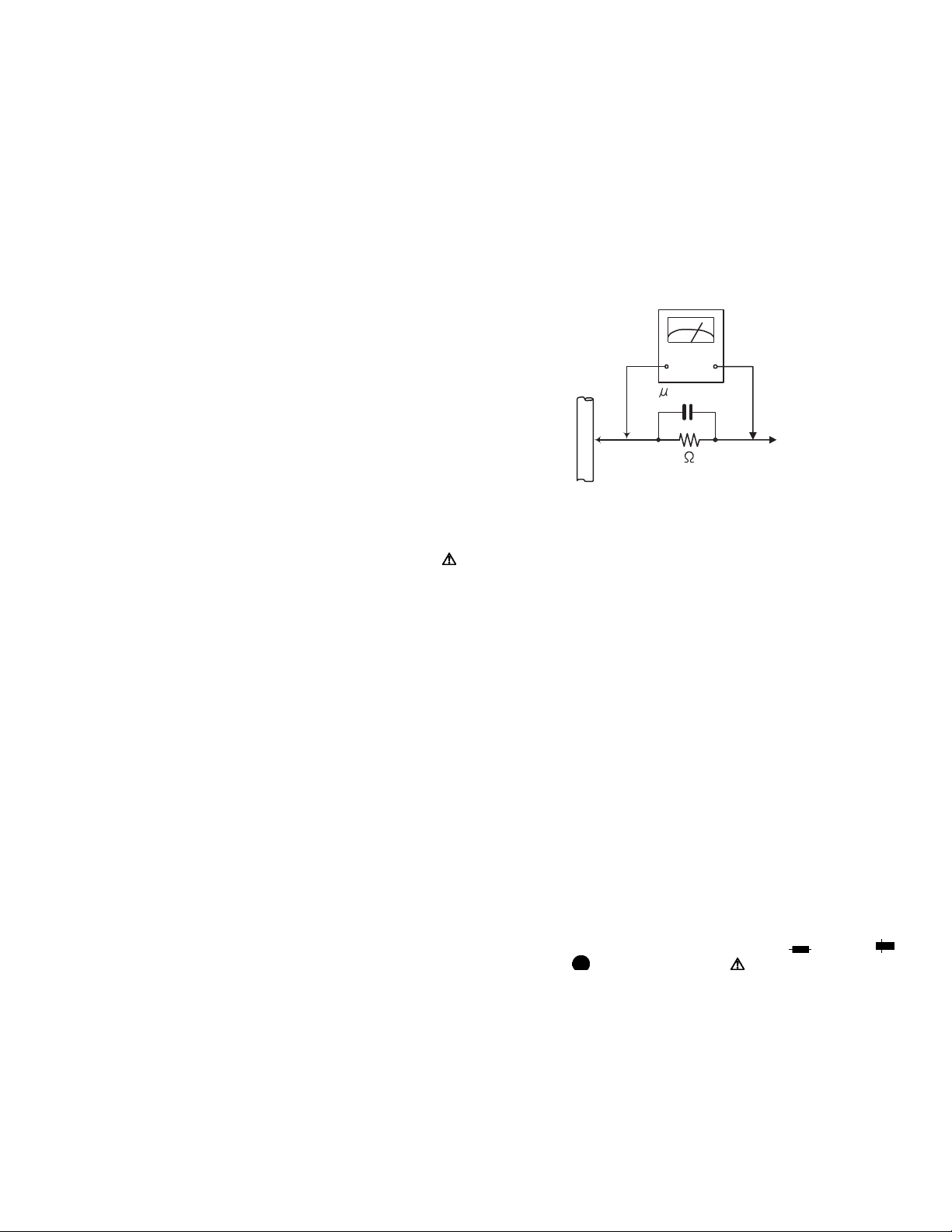
(5) Leakage shock hazard testing
After reassembling the product, always perform an isolation check on the exposed metal parts of the product (antenna terminals, knobs, metal cabinet, screw heads,
headphone jack, control shafts, etc.) to be sure the product
is safe to operate without danger of electrical shock.Do not
use a line isolation transformer during this check.
• Plug the AC line cord directly into the AC outlet. Using a
"Leakage Current Tester", measure the leakage current
from each exposed metal parts of the cabinet, particularly any exposed metal part having a return path to the
chassis, to a known good earth ground. Any leakage current must not exceed 0.5mA AC (r.m.s.).
• Alternate check method
Plug the AC line cord directly into the AC outlet. Use an
AC voltmeter having, 1,000Ω per volt or more sensitivity
in the following manner. Connect a 1,500Ω 10W resistor
paralleled by a 0.15µF AC-type capacitor between an ex-
posed metal part and a known good earth ground.
Measure the AC voltage across the resistor with the AC
voltmeter.
Move the resistor connection to each exposed metal
part, particularly any exposed metal part having a return
path to the chassis, and measure the AC voltage across
the resistor. Now, reverse the plug in the AC outlet and
repeat each measurement. Voltage measured any must
not exceed 0.75 V AC (r.m.s.). This corresponds to 0.5
mA AC (r.m.s.).
AC VOLTMETER
(Having 1000
ohms/volts,
or more sensitivity)
0.15 F AC TYPE
Place this
probe on
1500 10W
Good earth ground
1.2 Warning
(1) This equipment has been designed and manufactured to
meet international safety standards.
(2) It is the legal responsibility of the repairer to ensure that
these safety standards are maintained.
(3) Repairs must be made in accordance with the relevant
safety standards.
(4) It is essential that safety critical components are replaced
by approved parts.
(5) If mains voltage selector is provided, check setting for local
voltage.
1.3 Caution
Burrs formed during molding may be left over on some parts
of the chassis.
Therefore, pay attention to such burrs in the case of preforming repair of this system.
1.4 Critical parts for safety
In regard with component parts appearing on the silk-screen
printed side (parts side) of the PWB diagrams, the parts that are
printed over with black such as the resistor ( ), diode ( )
and ICP ( ) or identified by the " " mark nearby are critical
for safety. When replacing them, be sure to use the parts of the
same type and rating as specified by the manufacturer.
(This regulation dose not Except the J and C version)
each exposed
metal part.
(No.MB237)1-3
Page 4
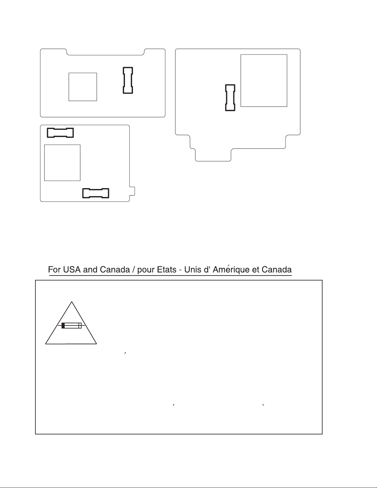
1.5 Importance administering point on the safety
Power supply / fuse board
2A-125V
F43
F41
500mA-200V
Power 2 board
8A-125V
F21
2A-125V
F42
Power 1 board
1-4 (No.MB237)
Caution: For continued protection against risk of fire,
replace only with same type 8 A/125 V for F21,
500 mA/200 V for F41, 2 A/125 V for F42 and F43.
This symbol specifies the type of fast operating fuse.
Precaution: Pour la protection continue contre les
risques d'incendie, remplacer uniquement par le
^
meme type: fusible 8 A/125 V pour le F21,
500 mA/200 V pour le F41, et 2 A/125 V pour les
F42 et F43.
Ce symbole specifie le type de fusible a action rapide.
Page 5

SECTION 2
SPECIFIC SERVICE INSTRUCTIONS
This service manual does not describe SPECIFIC SERVICE INSTRUCTIONS.
(No.MB237)1-5
Page 6
SECTION 3
DISASSEMBLY
3.1 Main body section
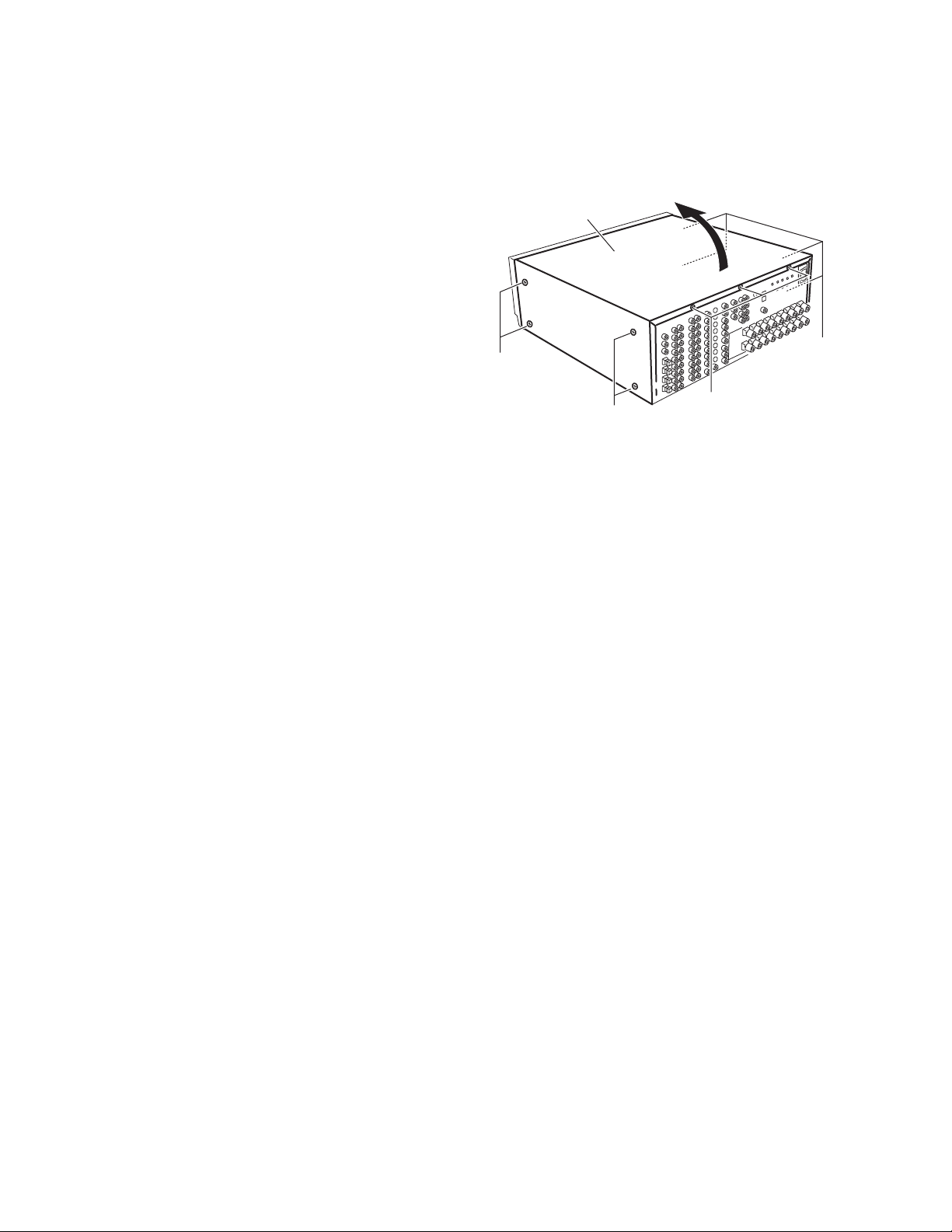
3.1.1 Removing the top cover
(See Fig.1)
(1) From the back sides of the main body, remove the three
screws A attaching the top cover.
(2) From the both sides of the main body, remove the four
screws B attaching the top cover.
(3) Take out the top cover upward in the direction of the arrow.
Top cover
B
B
B
A
Fig.1
1-6 (No.MB237)
Page 7
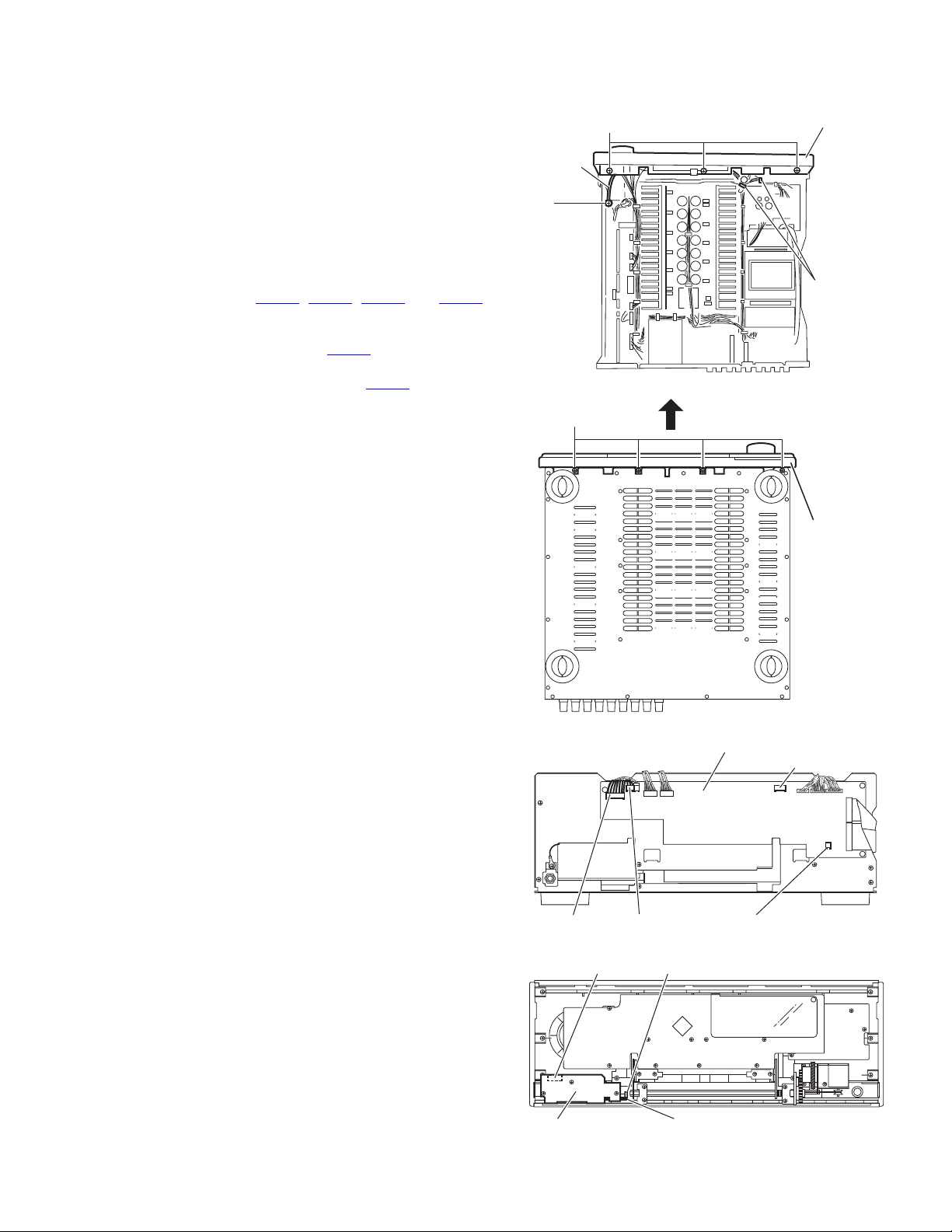
3.1.2 Removing the front panel assembly
(See Figs.2 to 5)
• Prior to performing the following procedure, remove the top
cover.
(1) From the top side of the main body, cut off the tie bands fix-
ing the wire. (See Fig.2)
(2) Remove the three screws C attaching the front panel as-
sembly. (See Fig.2)
(3) Remove the screw D attaching the lug wire. (See Fig.2)
(4) From the bottom side of the main body, remove the four
screws E attaching the front panel assembly and take out
the front panel assembly forward. (See Fig.3)
(5) From the front side of the main body, disconnect the wire
from the connectors CN971
on the system control board. (See Fig.4)
(6) From the reverse side of the front panel assembly, discon-
nect the wire from the connector CN973
board. (See Fig.5)
(7) Disconnect the wire from the connector CN373
DIGITAL in board. (See Fig.5)
Reference:
• When attaching the screws C, attach the earth wire with it.
(See Fig.2)
• When attaching the screws D, attach the lug wire with it.
(See Fig.2)
, CN977, CN983 and CN985
on the front AV in
on the front
Lug wire
D
E
C
Front panel assembly
Tie bands
Fig.2
CN973
Front panel
assembly
Fig.3
System control board
CN985
CN971CN977CN983
Fig.4
CN373
Front AV in board
Front DIGITAL in board
Fig.5
(No.MB237)1-7
Page 8
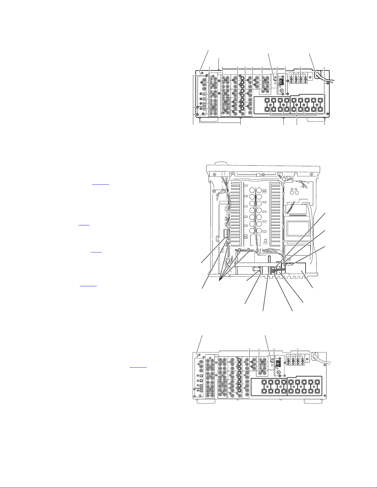
3.1.3 Removing the rear panel
(See Fig.6)
• Prior to performing the following procedure, remove the top
cover.
(1) From the top side on the main body, remove the screw F
attaching the rear panel.
(2) From the bottom side on the main body, remove the four
screws G attaching the rear panel.
(3) From the back side on the main body, remove the fifty-two
screws H attaching each board to the rear panel.
Reference:
When attaching the screws F, attach the lug wire with it.
Rear panel
F
H
H
Nat a Strain relief
H
H
H
H
H H
HH
H
3.1.4 Removing the V compo 2 board, RF remote unit, tuner unit and compu link board
(See Figs.7 and 8)
• Prior to performing the following procedure, remove the top
cover.
(1) From the top side of the main body, disconnect the card
wire from the connector CN581
(See Fig.7)
(2) From the back side of the main body, remove the two
screws J attaching V compo 2 board to the rear panel. (See
Fig.8)
(3) From the top side of the main body, disconnect the wire
from the connector CN1
(4) From the back side of the main body, remove the nut a at-
taching the RF remote unit to the rear panel. (See Fig.8)
(5) From the top side of the main body, disconnect the card
wire from the connector CN1
(6) From the back side of the main body, remove the two
screws K attaching the tuner unit to the rear panel. (See
Fig.8)
(7) From the top side of the main body, disconnect the wire
from the connector CN301
Fig.7)
(8) From the back side of the main body, remove the four
screws L attaching the compu link board to the rear panel.
(See Fig.8)
3.1.5 Removing the audio 7.1ch in board
(See Figs.7 and 8)
• Prior to performing the following procedure, remove the top
cover.
(1) From the top side of the main body, cut off the tie band fix-
ing the wire. (See Fig.7)
(2) Disconnect the wire from the connector CN201
dio signal 1 board. (See Fig.7)
(3) From the back side of the main body, remove the two
screws M attaching the audio 7.1ch in board to the rear
panel. (See Fig.8)
on the RF remote unit. (See Fig.7)
on the V compo 2 board.
on the tuner unit. (See Fig.7)
on the compu link board. (See
on the au-
CN201
Tie bands
Audio signal
1 board
V compu 2 board
Rear panel
G
CN581
G GH
Fig.6
RF remote unitAudio 7.1ch in board
Fig.7
Nat a
M
J K L
CN1
CN1
CN301
Compu link
board
Tuner unit
1-8 (No.MB237)
Fig.8
Page 9

3.1.6 Removing the Y/C separator board
(See Fig.9)
• Prior to performing the following procedure, remove the top
cover.
(1) From the top side of the main body, cut off the tie band fix-
ing the wire.
(2) Disconnect the connectors CN481
separator board, and take out the Y/C separator board upward.
3.1.7 Removing the system control board
(See Figs.10 and 11)
• Prior to performing the following procedures, remove the top
cover and front panel assembly.
(1) From the top side of the main body, cut off the tie bands fix-
ing the wires. (See Fig.10)
(2) Disconnect the wire from the connector CN45
2 board . (See Fig.10)
(3) Disconnect the wire from the connector CN25
er/fuse board. (See Fig.10)
(4) Disconnect the wire from the connector CN234
the audio signal 1 board. (See Fig.10)
(5) Disconnect the connector CN324
board. (See Fig.10)
(6) From the front side of the main body, disconnect the wires
from the connector CN963
tem control board. (See Fig.11)
(7) Remove the three plastic rivet, and take out the system
control board. (See Fig.11)
, CN964 and CN981 on the sys-
and CN482 on the Y/C
on the power
on the pow-
, CN208 on
on the audio signal 2
CN234
CN208
Tie bands
CN482
CN481
Fig.9
Tie bands
Audio signal 2 board
Fig.10
System control board Plastic rivetPlastic rivet
Y/C separator
board
CN45
Power 2 board
CN324
Power / fuse boardAudio signal 1 board
Tie
bands
CN25
CN981
Fig.11
CN963
(No.MB237)1-9
CN964
Page 10

3.1.8 Removing the DSP 1 board & DSP 2 board & shield cover
(See Fig.12)
• Prior to performing the following procedures, remove the top
cover, front panel assembly and rear panel.
(1) From the top side of the main body, cut off the tie bands fix-
ing the wires.
(2) Disconnect the connector CN631
(3) Disconnect the connector CN203 on the audio signal 1
board, and cut off the tie bands fixing the wire.
(4) Remove the two plastic rivet, and disconnect the connector
, CN643 on the DSP 2 board, and disconnect
CN633
on the DSP 1 board.
CN635
(5) Remove the screw N attaching the barrier to the shield cov-
er, and take out the shield cover.
on the DSP 2 board.
(Top view)
N
Barrier
Tie band
Shield cover
Tie bands
CN631
CN203
DSP 1
board
3.1.9 Removing the audio signal 1 board
(See Fig.13)
• Prior to performing the following procedures, remove the top
cover, front panel assembly and rear panel, DSP 1 board, DSP
2 board and shield cover.
(1) From the top side of the main body, disconnect the wires
from the connectors CN202
, CN223, CN224 and CN234 on the audio signal 1
CN218
board.
(2) Remove the plastic rivet, and disconnect the connectors
, CN206 and CN221 on the audio signal 1 board.
CN205
(3) Take out the audio signal 1 board.
, CN204, CN207, CN208,
CN633
DSP 2 board
Plastic rivet
CN204
CN202
CN224
CN234
CN205
Fig.12
CN208
CN206
CN221
Fig.13
CN635CN643 Plastic rivet
Audio signal 1 board
CN207
CN223
CN218
Audio signal 1 board
1-10 (No.MB237)
Page 11

3.1.10 Removing the audio signal 2 board & video board & S video board & component video board
(See Figs.14 and 15)
• Prior to performing the following procedures, remove the top
cover, rear panel, front panel assembly, Y/C separator board,
DSP 1 board, DSP 2 board, shield cover and audio signal 1
board.
(1) From the top side of the main body, disconnect the wire
from the connector CN324
(See Fig.14)
(2) Disconnect the audio signal 2 board from the connector
and CN6 on the main board. (See Fig.15)
CN15
(3) Disconnect the video board from the connector CN7
main board. (See Figs.14 and 15)
(4) Disconnect the S video board from the connector CN8
the main board. (See Figs.14 and 15)
(5) Disconnect the component video board from the connector
on the main board. (See Fig.15)
CN9
on the audio signal 2 board.
on the
on
Video board
CN324
S video board
Main board
Audio signal 2 board
Fig.14
Main board
Component
video board
CN15
CN6
CN7
CN8
CN9
Fig.15
(No.MB237)1-11
Page 12

3.1.11 Removing the main board
(See Figs.16 and 17)
• Prior to performing the following procedures, remove the top
cover, rear panel, front panel assembly, V compo 2 board, RF
remote unit, tuner unit, compu link board, audio 7.1ch in board,
Y/C separator board, DSP 1 board, DSP 2 board, shield cover,
audio signal 1 board, audio signal 2 board, video board, S video board and component video board.
(1) From the top side of the main body, cut off the tie bands fix-
ing the wire. (See Fig.16)
(2) Disconnect the wire from the connector CN62
lator board. (See Fig.16)
(3) Disconnect the wire from the CN44
(See Fig.16)
(4) Disconnect the wire from the connector CN743
speaker relay board. (See Fig.17)
(5) Disconnect the wire from the connector CN26
er/fuse board. (See Fig.16)
(6) Disconnect the card wire from the connector CN1
and the wire from the connector CN11 on the main board.
(See Fig.16)
(7) Remove the seven screws P attaching the main board, and
take out the main board. (See Fig.16)
on the power 2 board.
on the regu-
on the
on the pow-
, CN2
Regulator board
CN2
CN1 CN11
Power 2 board
CN62
CN44
3.1.12 Removing the speaker relay board
(See Fig.17)
• Prior to performing the following procedures, remove the top
cover and rear panel.
(1) Disconnect the wire from the connector CN741
and CN743 on the speaker relay board.
, CN742
P
Main board
Speaker relay board
Speaker relay board
CN743
CN743 CN742CN741
CN26
Power / fuse board
Fig.16
Fig.17
1-12 (No.MB237)
Page 13

3.1.13 Removing the regulator board
(See Fig.18)
• Prior to performing the following procedure, remove the top
cover.
(1) From top side of the main body, disconnect the wires from
the connectors CN61
the regulator board.
(2) Disconnect the wires from the connectors CN44
on the power 2 board.
(3) Remove the six screws Q attaching the regulator board.
Reference:
When attaching the screw Q, attach the earth wire with it.
3.1.14 Removing the power transformer 1 with the power 2 board
(See Fig.19)
• Prior to performing the following procedures, remove the top
cover and regulator board.
(1) From top side of the main body, disconnect the wire from
the connector CN46
(2) Remove the two screws R attaching the power transformer
1.
, CN62, CN63, CN64 and CN65 on
and CN45
and CN47 on the power 2 board.
CN62
CN65 CN64
CN61
Regulator boardQCN44
CN45
Fig.18
Power transformer 1
CN47
Power 2 boardCN63
Earth wireEarth wire
Q
Power 2 board
CN46
3.1.15 Removing the thermal SW 1 board
(See Fig.19)
• Prior to performing the following procedure, the top cover, side
panels, stay bkt and regulator board.
(1) From top side of the main body, remove the screw S at-
taching the thermal SW 1 board.
Thermal SW
1 board
R
S
Fig.19
(No.MB237)1-13
Page 14

3.1.16 Removing the power transformer 2
2
(See Figs.20 and 21)
• Prior to performing the following procedure, remove the top
cover, side panels, stay bkt and regulator board.
(1) From the top side of the main body, disconnect the wire
from the connector CN701
Fig.20)
(2) Remove the solder points PW81
trans 1 board. (See Fig.21)
(3) Remove the four screws T attaching the power transformer
2. (See Fig.21)
on the power amp. board. (See
and PW82 on the power
Fig.20
Power trans 1 board
PW81
T
Power amp. boardCN701
PW8
Power
transformer 2
Fig.21
1-14 (No.MB237)
Page 15

3.1.17 Removing the power transformer 3 with the power 1 board
V
V
(See Fig.22)
• Prior to performing the following procedure, remove the top
cover, side panels, stay bkt, regulator board, power transformer 1 and power transformer 2.
(1) From the top side of the main body, disconnect the wire
from the connector CN41
(2) Disconnect the wire from the connector CN48 on the power
supply temp compensation board.
(3) Remove the two screws U attaching the power transformer
3.
on the power 1 board.
U
Power supply temp
compensation board
3.1.18 Removing the power/fuse board
(See Fig.23)
• Prior to performing the following procedure, remove the top
cover, side panels, stay bkt, rear panel, regulator board and
power transformer 2.
(1) From the top side of the main body, disconnect the wire
from the connector CN25
(2) Remove the four screws V attaching the power/ fuse board.
(3) Remove the solder from the points PW21
and PW24 on the power/ fuse board.
on the power/ fuse board.
, PW22, PW23
CN41
CN25
Power 1 board
PW23 (red)
V
Power/ fuse board
Tie band
Power transformer3
Fig.22
PW21 (blue)
PW22 (brown)
Fig.23
CN48
PW24 (white)
(No.MB237)1-15
Page 16

3.1.19 Removing the head phone board
(See Figs.24 and 25)
• Prior to performing the following procedures, remove the top
cover, side panels, stay bkt and front panel assembly.
(1) From the top side of the main body, disconnect the wires
from the connector CN738
Fig.25)
(2) From the front side of the main body, remove the nut b fix-
ing the head phone board. (See Fig.24)
(3) Remove the screw W attaching the lug wire and bracket.
(See Fig.24)
Reference:
When attaching the screw W, attach the lug wire with it.
3.1.20 Removing the power amp. assembly
(See Figs.25 and 26)
• Prior to performing the following procedures, remove the top
cover, side panels, stay bkt, rear panel, front panel assembly,
system control board, DSP 1 board, DSP 2 board, audio signal
1 board, audio signal 2 board, video board, S video board, V
compo 1 board and speaker relay board.
(1) From top side of the main body, remove the three screws
X fixing the barriers, and remove the tow barriers. (See
Fig.25)
(2) Remove the eight screws Y attaching the power amp. as-
sembly. (See Figs.25 and 26)
(3) Take out the power amp. assembly in the direction of the
arrow. (See Fig. 26)
on the power amp. board. (See
Lug wire
Barrier
X
Bracket
Nut b
W
Head phone board
Fig.24
X
Power
amp.
assembly
Power
amp.
board
Y
Y
CN738
Fig.25
Power amp. assembly
1-16 (No.MB237)
Y
Fig.26
Page 17

3.2 Power amp. assembly section
• Remove the power amp. assembly from the main body.
(See "Removing the power amp. assembly".)
3.2.1 Removing the relay board & Rch amp. board & Lch amp. board & Cch amp. board & SL/SRch amp. board
(See Figs.1 to 3)
(1) From the top side of the amp. assembly, disconnect the
wires from the two connectors on each thermal compensation board. (See Fig.1)
(2) From the bottom side of the amp. assembly, remove the
two screws A attaching the relay board. (See Fig.2)
(3) Disconnect the wires from the five connectors on each
thermal compensation board. (See Fig.2)
(4) Disconecct the connectors CN712
, CN772, CN773, CN752 and CN753 on the each
CN813
amp. board of Lch, Cch, SL/SRch and Rch from the power
amp. board. (See Fig.2)
(5) From the top side of the relay board, disconnect the each
amp. board from the connectors CN721
and CN761 on the relay board. (See Fig.3)
, CN713, CN812,
, CN821, CN781
Power trans 1 board
T
Power
transformer 2
Lch amp. board
Cch amp. board
PW81
Fig.1
A
PW82
Connectors
T
CN713
CN813
CN773
CN753
Power amp. board
Cch amp. board
Lch amp. board
CN721
Relay board
A
Fig.2
CN712
CN812
CN772
CN752
SL/SRch amp. board
Rch amp. board
SL/SRch amp. board
Rch amp. board
CN761CN821
CN781
Fig.3
Relay board
(No.MB237)1-17
Page 18

3.2.2 Removing the thermal SW 2 board
(See Fig.4)
• Prior to performing the following procedure, remove the relay
board and the each amp. board of Lch, Cch, SL/SRch, Rch.
(1) From the top side of the amp. assembly, remove the screw
B attaching the thermal SW 2 board.
3.2.3 Removing the heat sink
(See Figs.4 to 6)
• Prior to performing the following procedure, remove the relay
board and the each amp. board of Lch, Cch, SL/SRch, Rch.
(1) From the both sides of the amp. assembly, remove the
eight screws C attaching the heat sink. (See Fig.4)
(2) From the top side of the amp. assembly, remove the eight
screws D attaching the power ICs. (See Fig.5)
(3) From the bottom side of the amp. assembly, remove the
twenty screws D attaching the power ICs. (See Fig.6)
D D
Heat sink
Thermal SW 2 board
Heat sink
B
C(both sides) C(both sides)
Fig.4
Fig.5
D D
Heat sink
1-18 (No.MB237)
Fig.6
Page 19

3.3 Front panel assembly section
• Remove the front panel assembly from the main body.
(See "Removing the front panel assembly".)
3.3.1 Removing the FL display board & front AV in board
(See Figs.1 and 2)
(1) From the front side of the front panel assembly, pull out the
volume knob to the forward and remove the nut a attaching
the FL display board. (See Fig.1)
(2) From the reverse side of the front panel assembly, remove
the three screws A attaching the front AV in board and take
out the front AV in board. (See Fig2)
(3) Remove the nine screws B attaching the FL display board.
(See Fig.2)
(4) Disconnect the wires from the connectors CN969
and CN982 on the FL display board. (See Fig.2)
, CN975
Front panel assembly
Front AV in board
B
A
Volume knob
Fig.1
FL display board
CN982 CN969 CN975
B
Fig.2
Nut a
(No.MB237)1-19
Page 20

3.3.2 Removing the power switch board & front DIGITAL in board
(See Fig.3)
• Prior to performing the following procedure, remove the FL dis-
play board.
(1) From the reverse side of the front panel assembly, remove
the four screws C attaching the power switch board and
take out the power switch board.
(2) Remove the screw D attaching the front DIGITAL in board
and take out the front DIGITAL in board.
3.3.3 Removing the door SW board
(See Fig.4)
• Prior to performing the following procedure, remove the FL dis-
play board.
(1) From the reverse side of the front panel assembly, remove
the two screws E attaching the door SW board.
(2) Take out the door SW board.
3.3.4 Removing the motor assembly & door input board
(See Figs.4 and 5)
• Prior to performing the following procedure, remove the FL dis-
play board and door SW board.
(1) From the reverse side of the front panel assembly, remove
the three screws F attaching the motor assembly. (See
Fig.4)
(2) Remove the belt and the two screws G attaching the motor
assembly. (See Fig.4)
(3) Remove the four screws H attaching the door and take out
the door to the forward. (See Fig.4)
(4) From the reverse side of the door, remove the six screws J
attaching the door input board. (See Fig.5)
D
Front DIGITAL in board CN373
Power switch board
Fig.3
Door
Door SW board
Motor assembly
Fig.4
HH G
E
Belt
C
G
F
J
Door input board Door
Fig.5
1-20 (No.MB237)
Page 21

SECTION 4
ADJUSTMENT
4.1 Adjustment of idling current
Measuring point Alignment point Measuring condition
Lch B903
Rch B911
Cch B907 & B908 VR801
SLch B907 & B908 VR771
SRch B909 & B910 VR772
SBLch B901 & B902 VR702
SBRch B913 & B914 VR752
Attention:
This adjustment does not obtain a correct adjustment value immediately after the amplifier is used (state that an internal temperature
has risen).
Please adjust immediately after using the amplifier after turning off the power supply of the amplifier and falling an internal temperature.
Adjustment method
(1) Prior to turning the power ON, fully turn the adjusting resistor (VR701
terclockwise direction and connect the DC voltmeter to the measuring terminal (B901-B902, B903-B904, B905-B906, B907-
B908, B909-B910, B911-B912, B913-B914).
(2) Adjust the resistor so that the measured value becomes 2.0mV just after the power supply is turned on.
(3) Adjust the resistor so that the measured value becomes 2.5mV more than 60 seconds after the power supply is turned on.
(4) After stability is 1.0-4.0mV.
& B904 VR701 No load and No signal.Rated line voltage
& B912 VR751
SURROUND : OFF
Room temperature : 20~25ºC
, VR702, VR751, VR752, VR771, VR772, VR801) coun-
Refer to following page "Idling Current graph".
* It is not abnormal though the idling current might not become 0mA even if it is finished to turn variable resistance (VR701
, VR752, VR771, VR772, VR801) in the direction of counterclockwise.
VR751
B901, B902 (SBLch)
B903, B904 (Lch)
VR701 (Lch)
VR702 (SBLch)
B905, B906 (SLch)
VR801 (Cch)
B907, B908 (Cch)
VR771 (SLch)
VR772 (SRch)
B909, B910 (SRch)
VR751 (Rch)
VR752 (SBRch)
B911, B912 (Rch)
, VR702,
B913, B914 (SBRch)
(No.MB237)1-21
Page 22

4.2 Idling Current graph (1/2)
4
3.5
3
2.5
2
1.5
1
Voltage at measering point(mV)
0.5
SL ch / SR ch
SL ch
SR ch
0
02468101214
Time(Min)
SBL ch / SBR ch
4
3.5
3
2.5
2
1.5
1
Voltage at measering point(mV)
SBL ch
SBR ch
0.5
0
02468101214
1-22 (No.MB237)
Time(Min)
Page 23

4.3 Idling Current graph (2/2)
4
3.5
3
2.5
2
1.5
1
Voltage at measering point(mV)
0.5
L ch / R ch
L ch
R ch
0
02468101214
Time(Min)
C ch
4
3.5
3
2.5
2
1.5
1
Voltage at measering point(mV)
0.5
0
0246
8101214
Time(Min)
(No.MB237)1-23
Page 24

SECTION 5
TROUBLESHOOTING
This service manual does not describe TROUBLESHOOTING.
1-24 (No.MB237)
Page 25

(No.MB237)1-25
Page 26

Victor Company of Japan, Limited
AV & MULTIMEDIA COMPANY AUDIO/VIDEO SYSTEMS CATEGORY 10-1,1chome,Ohwatari-machi,Maebashi-city,371-8543,Japan
(No.MB237)
Printed in Japan
WPC
 Loading...