

Page 1
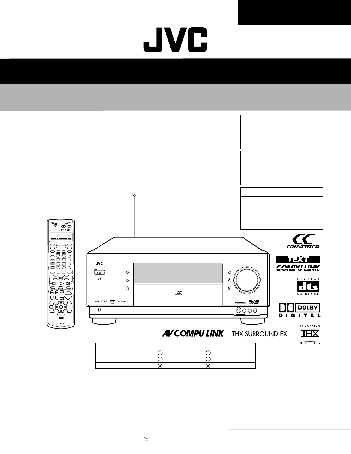
RX-DP10VBK/RX-DP10VSL
SERVICE MANUAL
AUDIO/VIDEO CONTROL RECEIVER
RX-DP10VBK
RX-DP10VBK
J ---------------------- U.S.A.
RX-DP10VSL
Area suffix
RX-DP10VSL
RX-DP10RSL
TRANSMITLEARN
SUB ROOM
MAIN ROOM
MAIN ROOM
SUB ROOM
ON/OFF ON/OFF
SUB ROOM LEARNMAIN ROOM
DVD
DVD MULTI
VCR 1 VCR 2
ANALOG/DIGITAL
INPUT
123
SOUND
456
/P
7
10
RETURN
TEST
ON/OFF ON/OFFMODE
LINE DIRECT
SLEEP DIMMER
/ REW
DOWN UP
REC
CHANNEL
TV VOL
SETUP
MENU
TEXT
DISPLAY
DVD
MENU
RM-SRXDP10J
A/V CONTROL RECEIVER
STANDBY
TV/CATV/DBS VCR 1
STANDBY/ON STANDBY/ON
PHONO
TAPE/MD
FMVIDEOTV/DBS
89
FM MODE
DSP THXSURROUND
CC CONVERTER
PLAY
TUNING
STOP PAUSE
TV/VIDEO
MUTING
SET
LIGHT
REMOTE CONTROL
RX-DP10RSL
Area suffix
C -------------------- Canada
RX-DP10RSL
Area suffix
B ------------------------- U.K.
E ----- Continental Europe
ON
CD
CDR
AM
EFFECT
ROOM SIZE
LIVENESS
WALL
+
100
+
100
TV
CATV/
DBS
FF/
VOLUME
ADJUST
MENU
EXIT
STANDBY
STANDBY/ON
DIGITAL
DIGITAL
SURROUND
PHONES
CC CONVERTER
MAIN ROOM
ON/OFF
SUB ROOM
ON/OFF
RX-DP10V
AUDIO/VIDEO CONTROL RECEIVER
DIMMER
DOOR
DOOR
DOWN
EN ------ Northern Europe
MASTER VOLUME
UP
VIDEO L—AUDIO—R
S-VIDEO
VIDEO
Model RF remote unit Video SEP board Color
RX-DP10VBK Black
RX-DP10VSL
Silver
SilverRX-DP10RSL
Contents
Safety precautions --------------------------------------------------------1-2
Importance administering point on the safety --------------------- 1-4
Disassembly method -----------------------------------------------------1-5
Adjustment method -------------------------------------------------------1-14
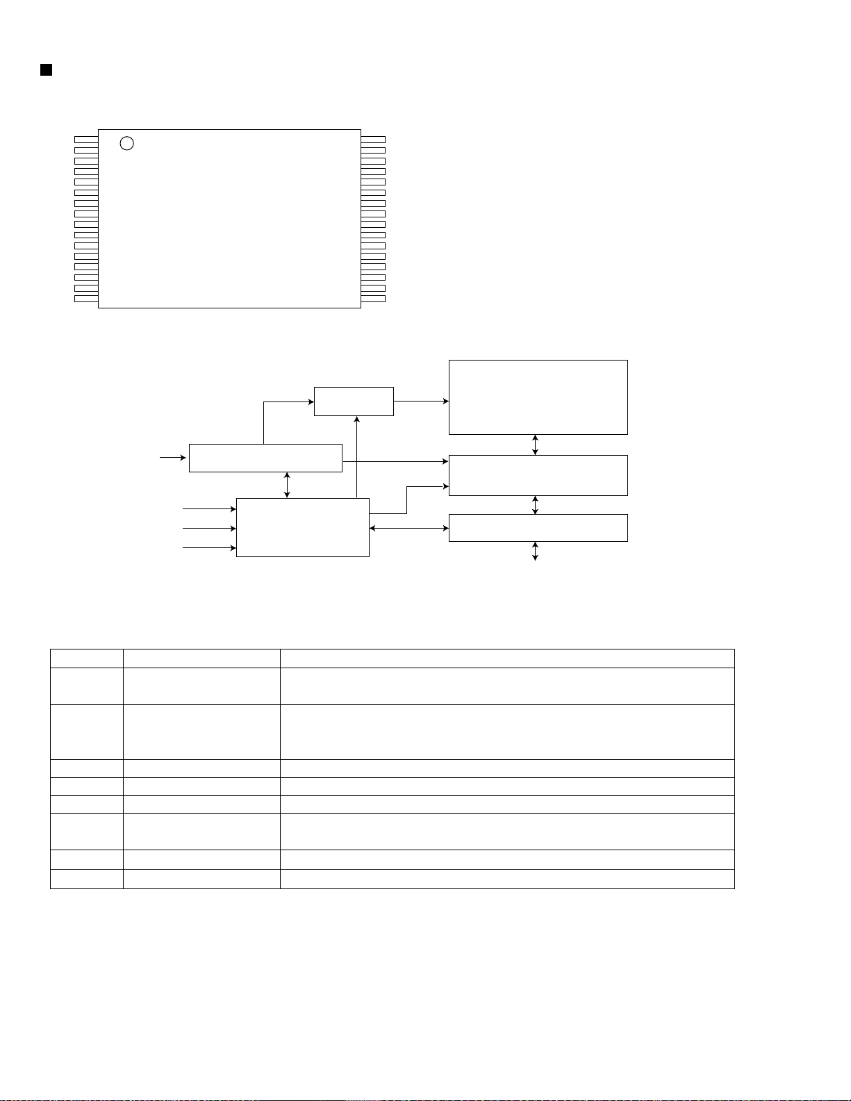
Description of major ICs -------------------------------------------------1-16~37
COPYRIGHT 2001 VICTOR COMPANY OF JAPAN, LTD.
No.21025
Sep. 2001
Page 2
RX-DP10VBK/RX-DP10VSL
RX-DP10RSL
1. This design of this product contains special hardware and many circuits and components specially for safety
purposes. For continued protection, no changes should be made to the original design unless authorized in
writing by the manufacturer. Replacement parts must be identical to those used in the original circuits. Services
should be performed by qualified personnel only.
2. Alterations of the design or circuitr y of the product should not be made. Any design alterations of the product
should not be made. Any design alterations or additions will void the manufacturer's warranty and will further
relieve the manufacture of responsibility for personal injury or property damage resulting therefrom.
3. Many electrical and mechanical parts in the products have special safety-related characteristics. These
characteristics are often not evident from visual inspection nor can the protection afforded by them necessarily
be obtained by using replacement components rated for higher voltage, wattage, etc. Replacement par ts which
have these special safety characteristics are identified in the Parts List of Service Manual. Electrical
components having such features are identified by shading on the schematics and by ( ) on the Parts List in
the Service Manual. The use of a substitute replacement which does not have the same safety characteristics
as the recommended replacement parts shown in the Parts List of Service Manual may create shock, fire, or
other hazards.
4. The leads in the products are routed and dressed with ties, clamps, tubings, barriers and the like to be
separated from live parts, high temperature parts, moving parts and/or sharp edges for the prevention of
electric shock and fire hazard. When service is required, the original lead routing and dress should be
observed, and it should be confirmed that they have been returned to normal, after re-assembling.
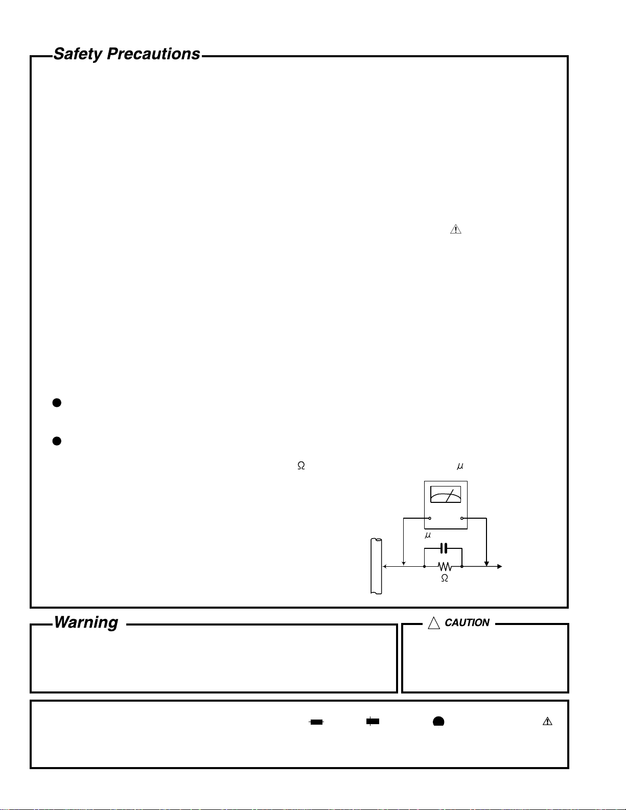
5. Leakage current check (Electrical shock hazard testing)
After re-assembling the product, always perform an isolation check on the exposed metal parts of the product
(antenna terminals, knobs, metal cabinet, screw heads, headphone jack, control shafts, etc.) to be sure the
product is safe to operate without danger of electrical shock.
Do not use a line isolation transformer during this check.
Plug the AC line cord directly into the AC outlet. Using a "Leakage Current Tester", measure the leakage
current from each exposed metal parts of the cabinet, particularly any exposed metal part having a return
path to the chassis, to a known good earth ground. Any leakage current must not exceed 0.5mA AC (r.m.s.).
Alternate check method
Plug the AC line cord directly into the AC outlet. Use an AC voltmeter having, 1,000 ohms per volt or more
sensitivity in the following manner. Connect a 1,500 10W resistor paralleled by a 0.15 F AC-type capacitor
between an exposed metal part and a known good earth ground.
Measure the AC voltage across the resistor with the AC
voltmeter.
Move the resistor connection to each exposed metal part,
particularly any exposed metal part having a return path to
the chassis, and measure the AC voltage across the resistor.
Now, reverse the plug in the AC outlet and repeat each
measurement. Voltage measured any must not exceed 0.75 V
AC (r.m.s.). This corresponds to 0.5 mA AC (r.m.s.).
0.15 F AC TYPE
1500 10W
Good earth ground
AC VOLTMETER
(Having 1000
ohms/volts,
or more sensitivity)
Place this
probe on
each exposed
metal part.
!
1. This equipment has been designed and manufactured to meet international safety standards.
2. It is the legal responsibility of the repairer to ensure that these safety standards are maintained.
3. Repairs m ust be made in accordance with the relevant safety standards.
4. It is essential that safety critical components are replaced by approved parts.
5. If mains voltage selector is provided, check setting for local voltage.
Burrs formed during molding may
be left over on some parts of the
chassis. Therefore, pay attention to
such burrs in the case of
preforming repair of this system.
In regard with component parts appearing on the silk-screen pr inted side (parts side) of the PWB diagrams, the
parts that are printed over with black such as the resistor ( ), diode ( ) and ICP ( ) or identified by the " "
mark nearby are critical for safety.
When replacing them, be sure to use the parts of the same type and rating as specified by the manufacturer.
(Except the J&C version)
1-2
Page 3
RX-DP10VBK/RX-DP10VSL
RX-DP10RSL
(U.K only)
1. This design of this product contains special hardware and many circuits and components specially
for safety purposes. For continued protection, no changes should be made to the original
design unless authorized in writing by the manufacturer. Replacement parts must be identical to
those used in the original circuits.
2. Any unauthorised design alterations or additions will void the manufacturer's guarantee ; further more the
manufacturer cannot accept responsibility f or personal injury or property damage resulting therefrom.
3. Essential safety critical components are identified by ( ) on the Parts List and by shading on the
schematics, and must never be replaced by parts other than those listed in the manual. Please note
however that many electrical and mechanical parts in the product have special safety related
characteristics. These characteristics are often not evident from visual inspection. Parts other than
specified by the manufacturer may not have the same safety characteristics as the recommended
replacement parts shown in the Parts List of the Service Manual and may create shock, fire, or
other hazards.
4. The leads in the products are routed and dressed with ties, clamps, tubings, barriers and the
like to be separated from live parts, high temperature parts, moving parts and/or sharp edges
for the prevention of electric shock and fire hazard. When service is required, the or iginal lead
routing and dress should be observed, and it should be confirmed that they have been returned
to normal, after re-assembling.
1. Service should be performed by qualified personnel only.
2. This equipment has been designed and manufactured to meet international safety standards.
3. It is the legal responsibility of the repairer to ensure that these safety standards are maintained.
4. Repairs must be made in accordance with the relevant safety standards.
5. It is essential that safety critical components are replaced by approved parts.
6. If mains voltage selector is provided, check setting for local voltage.
!
Burrs formed during molding may be left over on some parts of the chassis. Therefore,
pay attention to such burrs in the case of preforming repair of this system.
1-3
Page 4
RX-DP10VBK/RX-DP10VSL
RX-DP10RSL
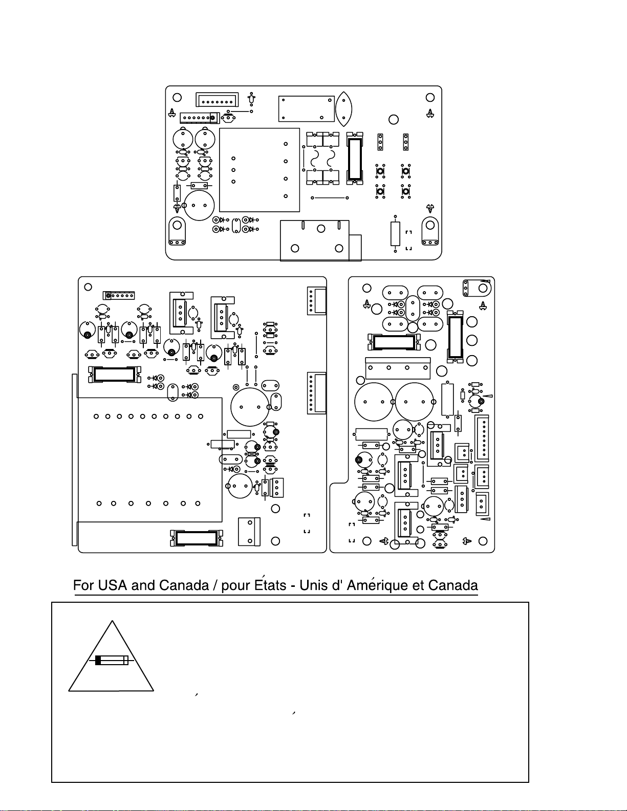
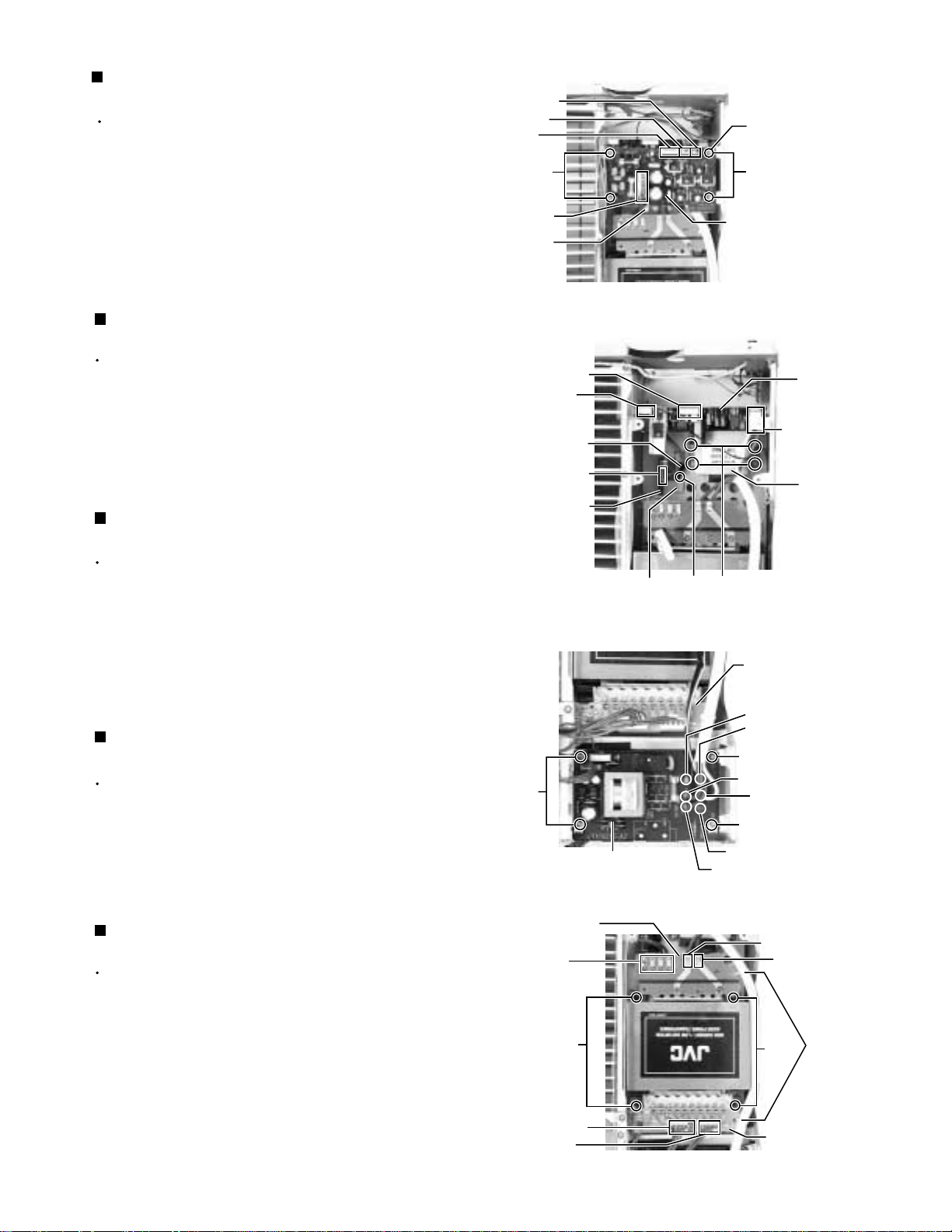
Importance administering point on the safety
C50
WR44
D51
D46
C49
R48
Q50
FC43FC44
C48
R47
B118
Q49
2A 125V
F42
LVA10215-A3
CN25
D25
WR26
C25
C27
D27
D26
Q22 Q23
R23
R24
R25
C24
C23
R22
EP22
C47
HS42
D49
Q42
D50
R45
R46
Q53 Q54
D43
D44
F41
C46
B117
R44
Q52
C41
1A 125V
FC42
C45
D48
B309
Q21
C26
D22
D24
D23
D21
C22
HS41
Q41
D47
R43
D41
D42
C43
D45
D52
C44
R41
R42
Q51
TW41
B204
C42
R50
R49
B116
TH41
D53
C51
T41
FC41
RY21
FC26
B307
FC25
T21
CN42CN43
R54
Q55
R55
B120
B308
Q56
C55
B203
C56
R53
C54
C53
D56
Q48
Q46
R52
C52
B119
Q47
D55
R51
Q45
CN41
LVA10215-A2
C21
FC24FC23
FC22
TA1
PW23
B110
B111
8A 125V
FC21
F21
B112
B511
J21
F61
C71
C69
B113
PW22
R21
LVA10215-A4
C63
D62
D61
C62
2A 125V
FC61FC62
C66
R61
R64
C70
D67
D68
R65
R62
D65
D66
R63
TA2
PW24
B109
B108
B115
B114
PW21
EP21
EP61
C61
CN61
C67
C73
D70
R68
Q62
HS62
C68
Q61
HS61
C65
D64
D63
C64
F62
2A 125V
FC63 FC64
R69
D71
R70
R66
C72
D69
Q63
CN67
HS63
R74
B306
CN66
C75
R72
C76
D73
R73
Q66
Q65
C74
R71
R67
CN63
B130
CN64
B206
Q64
CN65
D72
1-4
Caution: For continued protection against risk of
fire, replace only with same type 1A/125V for
F41, 2A/125V for F61, F62 and F42, 8A/ 125V for F21.
This symbol specifies type of fast operating fuse.
Precaution: Pour eviter risques de feux, remplacez
le fusible de surete de et F41 comme le meme type
que 1A/125V, et 2A/125V pour F61, F62 et F42,
8A/125V pour F21. Ce sont des fusibles suretes qui
^
functionnes rapide.
Page 5
RX-DP10VBK/RX-DP10VSL
RX-DP10RSL
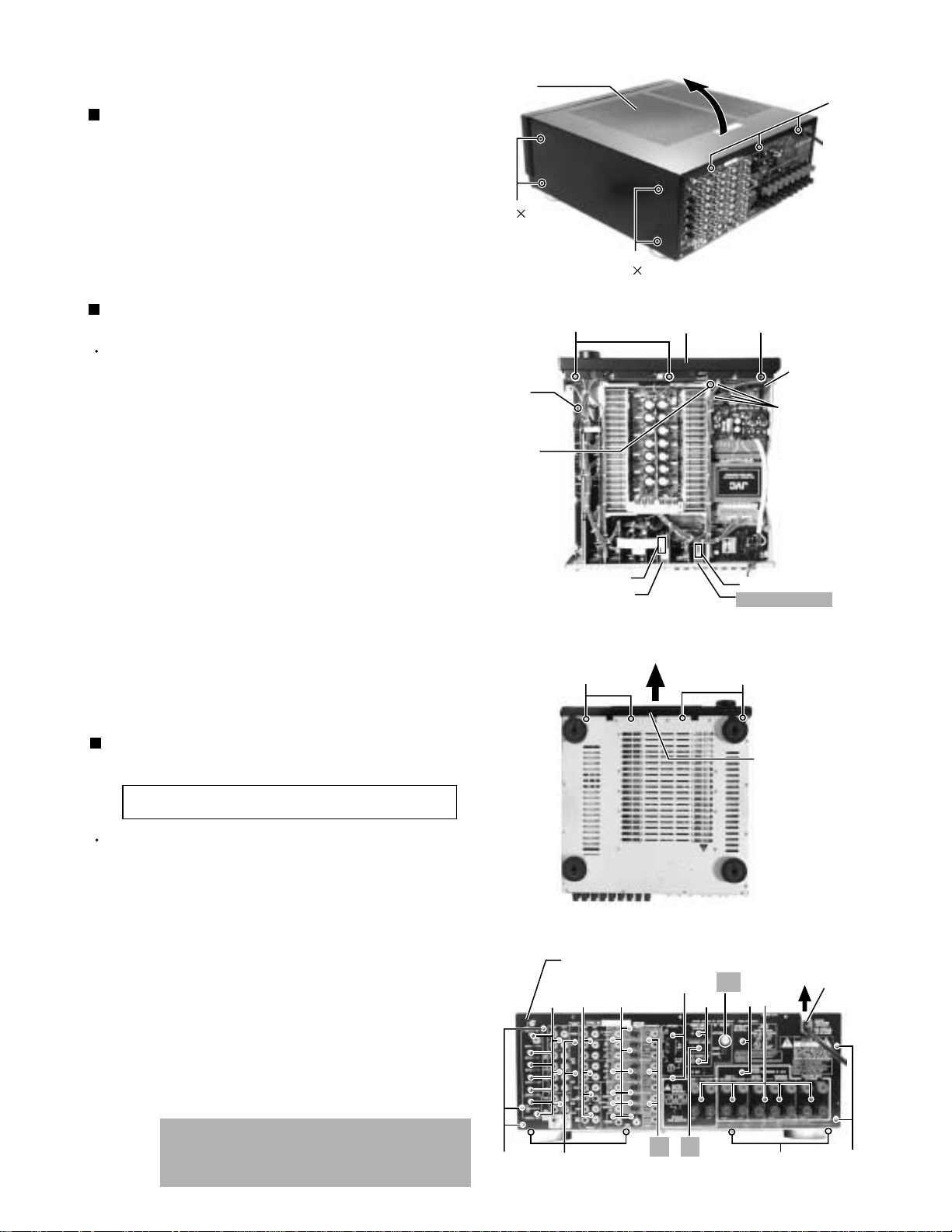
Disassembly method
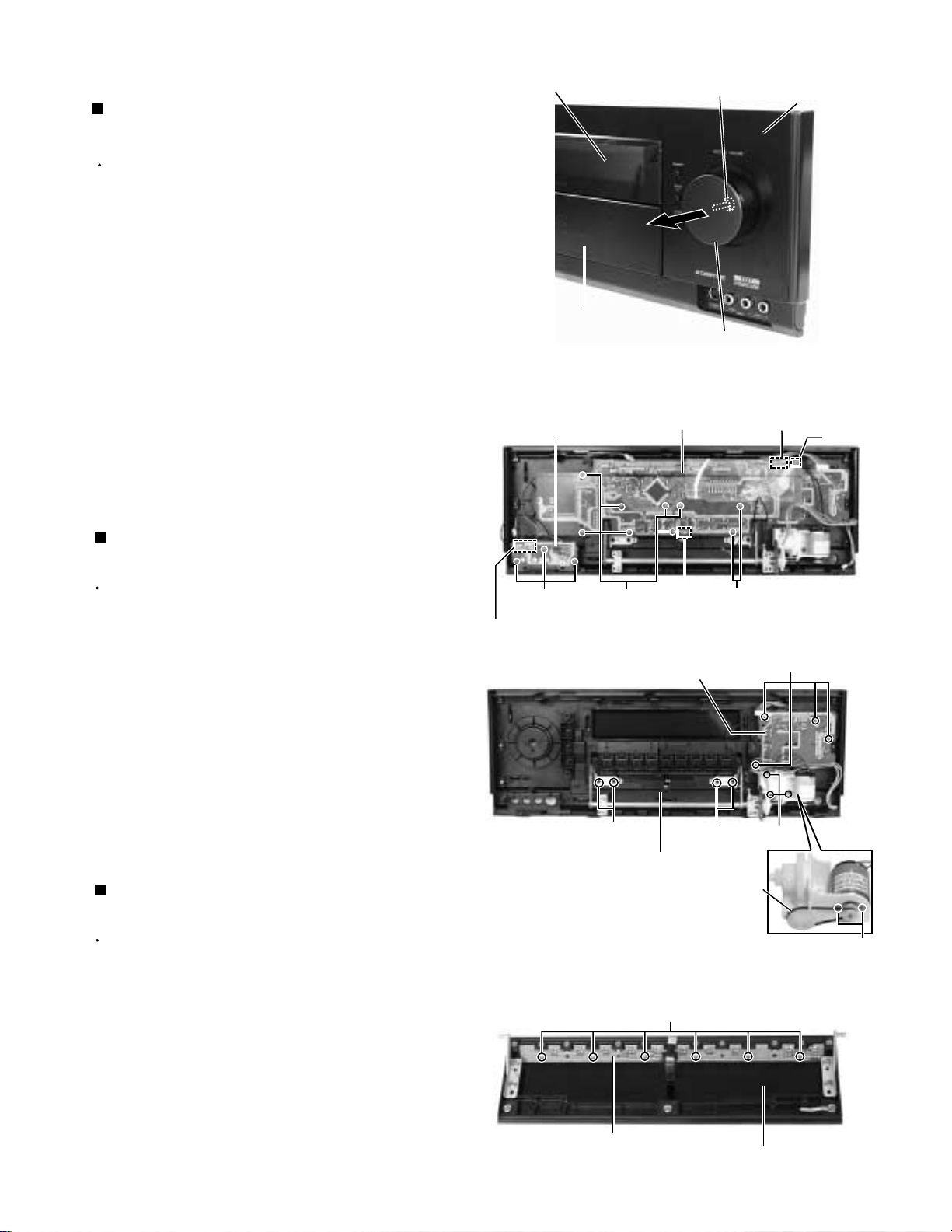
Removing the top cover (See Fig.1)
Remove the eight screws A attaching the top cover
1.
on both sides of the body.
Remove the three screws B on the back of the body.
2.
Remove the top cover from behind in the direction of
3.
the arrow while pulling both sides outward.
Removing the front panel assembly
(See Fig.2 and 3)
Prior to performing the following procedure, remove
the top cover.
Cut off the tie band fixing the harness.
1.
Disconnect the harness from the connector CN971,
2.
CN977, CN983 and CN985 on the system control
board (see fig.5) and CN973 on the front AV in board
(see Front panel assembly section/ fig.2).
Top cover
A
4
a
(fixing the
earth wire)
b
(fixing the
earth wire)
A
4
Front panel assembly
C
B
Fig.1
C
Harness
band
Tie band
Remove the screws a and b, and remove each earth
3.
wires.
Remove the three screws C attaching the front panel
4.
assembly.
Remove the four screws D attaching the front panel
5.
assembly on the bottom of the body. Detach the front
panel assembly toward the front.
Removing the tuner unit & RF remote unit
(See Fig.2 and 4)
Note : RF remote unit is not in B/E/EN version.
Prior to performing the following procedure, remove
the top cover.
1.
Disconnect the card wire from the connector CN1 on
the tuner unit.
2.
Remove the two screws E' attaching the tuner unit to
the rear panel.
3.
Disconnect the harness from the connector CN1 on
the RF remote unit.
Tuner unit
D
Rear panel
E
CN1
CN1
Fig.2
RF remote unit
D
Front panel
assembly
Fig.3
Power cord
E''
EE
E'
E
F
E
stopper
4.
Remove the nut E'' attaching the RF remote unit to
the rear panel.
THE INTRODUCTORY NOTES in Figs :
Gray parts do not correspond to B/E/EN
version.
E E
FF F
Fig.4
F
1-5
Page 6
RX-DP10VBK/RX-DP10VSL
RX-DP10RSL
Removing the rear panel (See Fig.4)
Prior to performing the following procedure, remove
the top cover.
Remove the power cord stopper from the rear panel
1.
by moving it in the direction of the arrow.
Remove the thirty six (B/E/EN version is thirty two)
2.
screws E attaching the each boards to the rear panel
on the back of the body.
Remove the thirteen screws F attaching the rear
3.
panel on the back of the body and bottom.
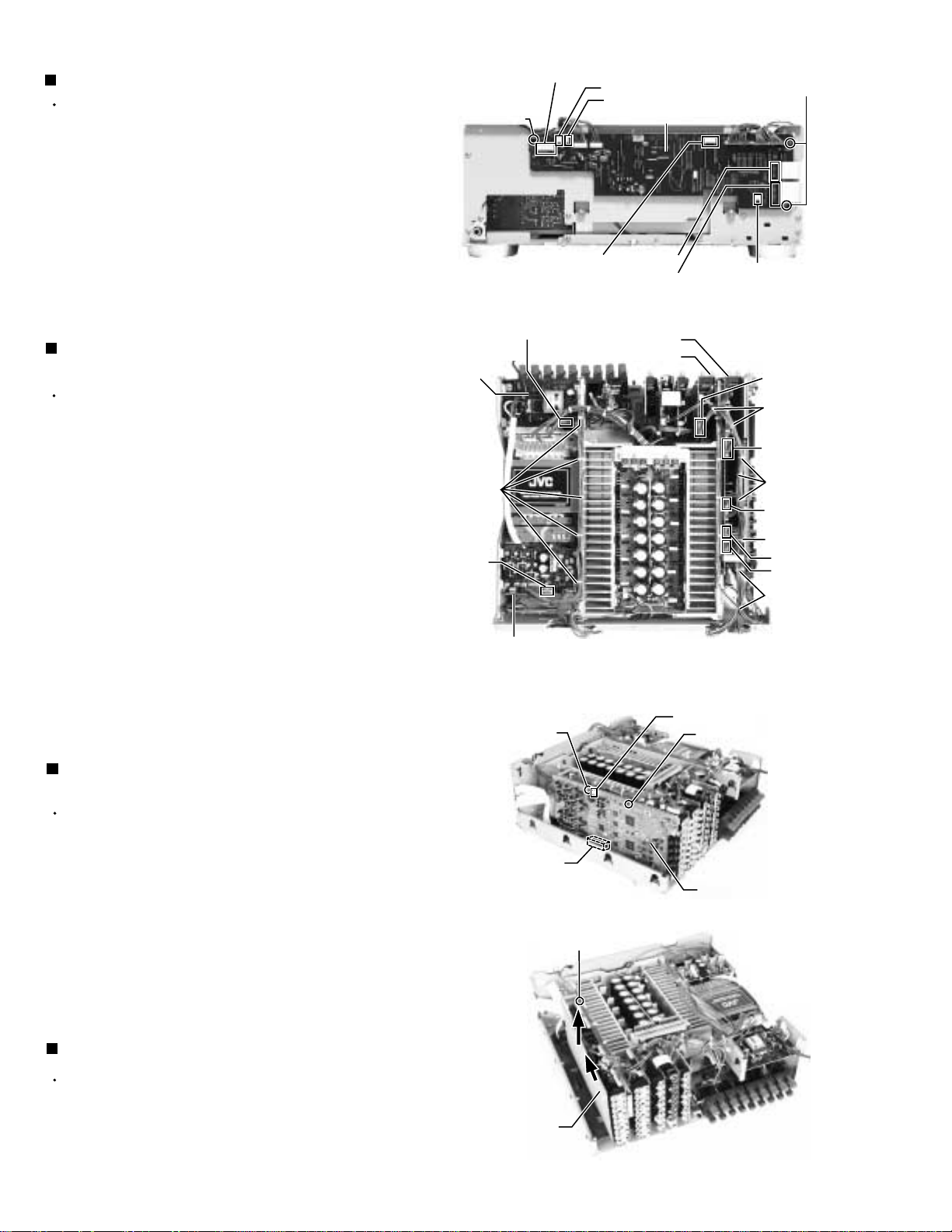
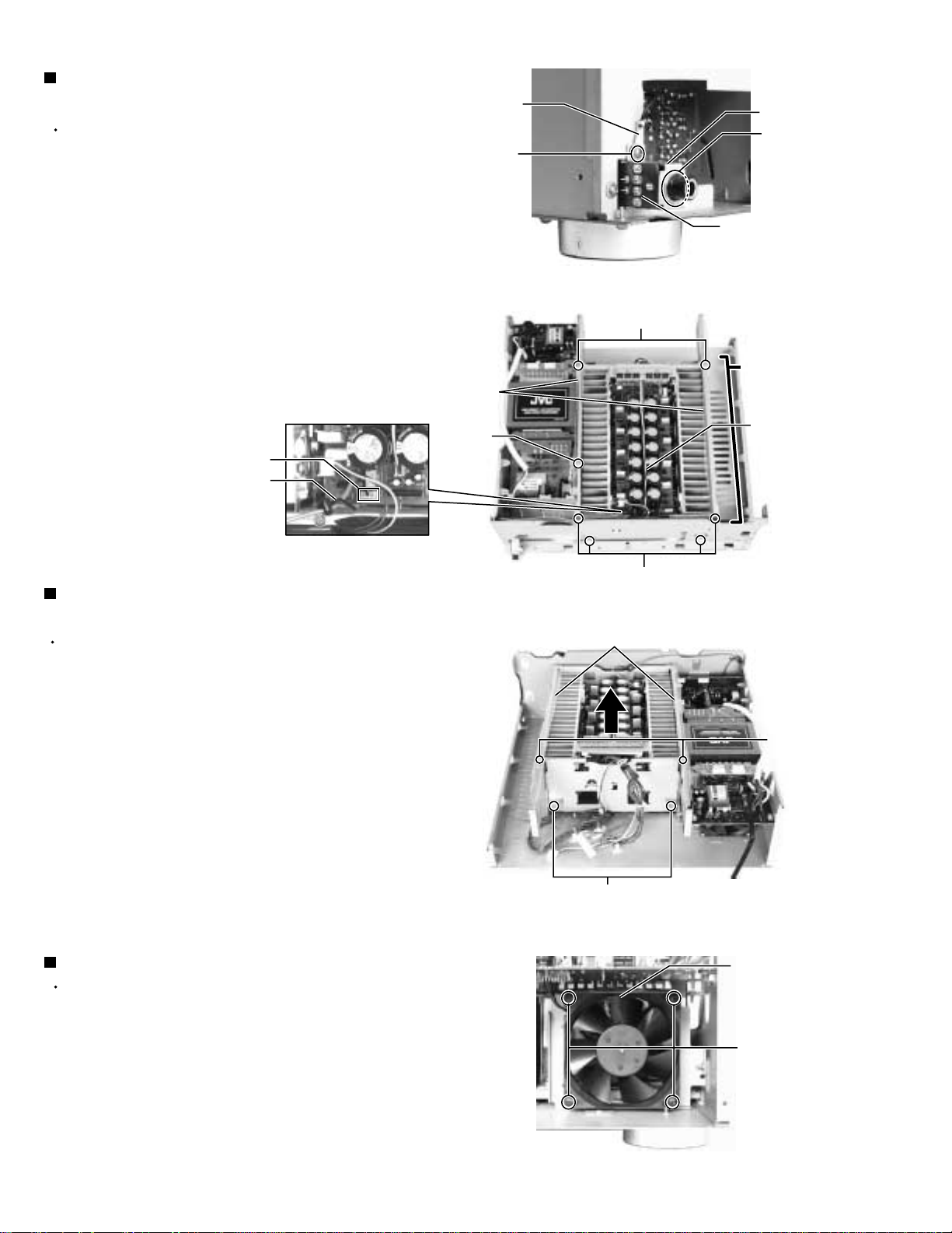
Removing the system control board
(See Fig.5 and 6)
Prior to performing the following procedure, remove
the top cover and front panel assembly.
Disconnect the card wires and harness from
1.
connector CN963, CN964 and CN981 on the system
control board.
Cut off the tie bands fixing the harnesses.
2.
Disconnect the harness from connector CN43 on the
3.
power supply 2 board and CN25 on the power/ fuse
board.
Disconnect the connector CN324 on the audio signal
4.
2 board and CN205, CN234, CN208(J/C only) on the
audio signal 1 board.
CN983
Plastic rivet
CN25
Power/ fuse
board
Audio signal 1 board
Audio signal 2 board
Tie band
CN43
Power supply 2 board
CN985
CN977
CN981
System control board
CN963
CN964
Fig.5
Fig.6
Plastic rivet
CN971
CN324
Tie band
CN203
Tie band
CN208
(J/C only)
Tie band
CN234
CN205
Tie band
Remove the three plastic rivet.
5.
Removing the DSP board
(See Fig.6 and 7)
Prior to performing the following procedure, remove
the top cover and the rear panel.
Disconnect the connector CN631 on the DSP board.
1.
Disconnect the connector CN203 on the audio signal
2.
1 board.
Removing the two plastic rivet and disconnect the
3.
connector CN633 on the DSP board.
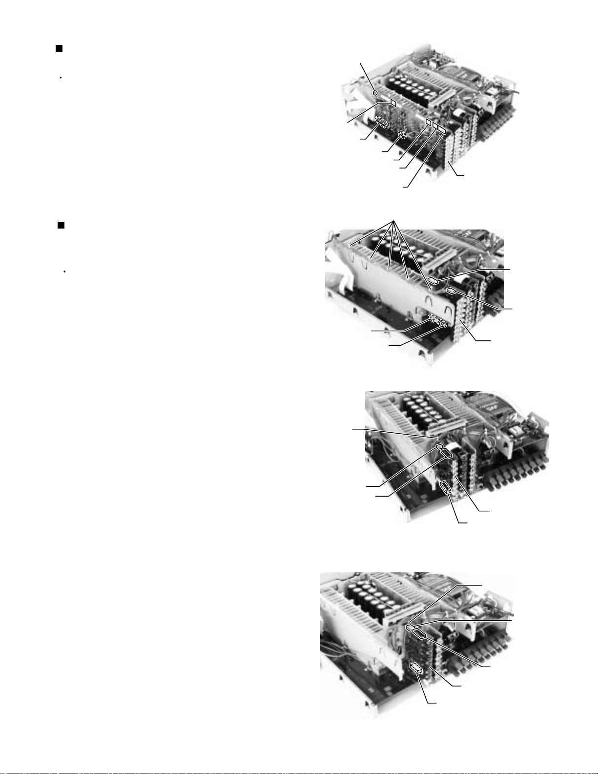
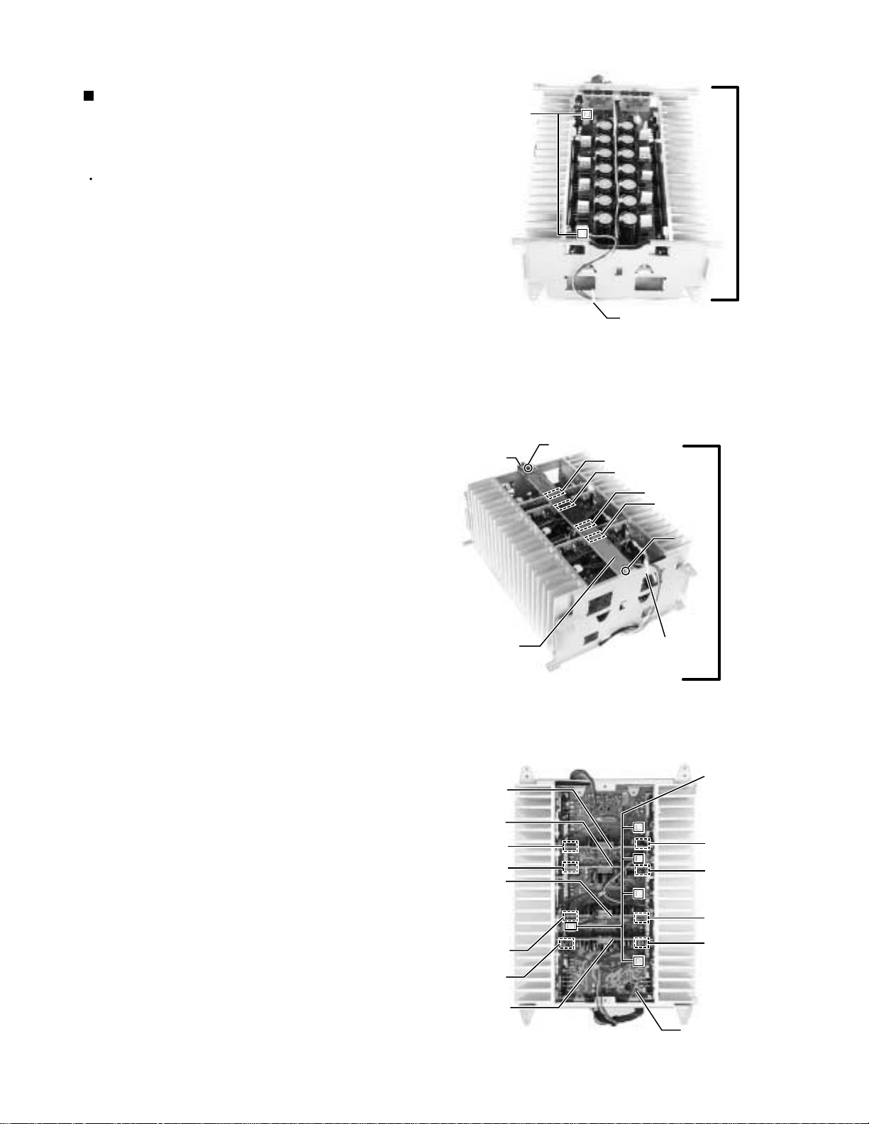
Removing the shield cover (See Fig.8)
Prior to performing the following procedure, remove
the top cover and the rear panel.
Removing the screw G attaching the shield cover.
1.
Plastic rivet
CN633
Shield cover
CN631
Plastic rivet
DSP board
Fig.7
G
Shift the shield cover before, and pull upward.
2.
1-6
Fig.8
Page 7
RX-DP10VBK/RX-DP10VSL
RX-DP10RSL
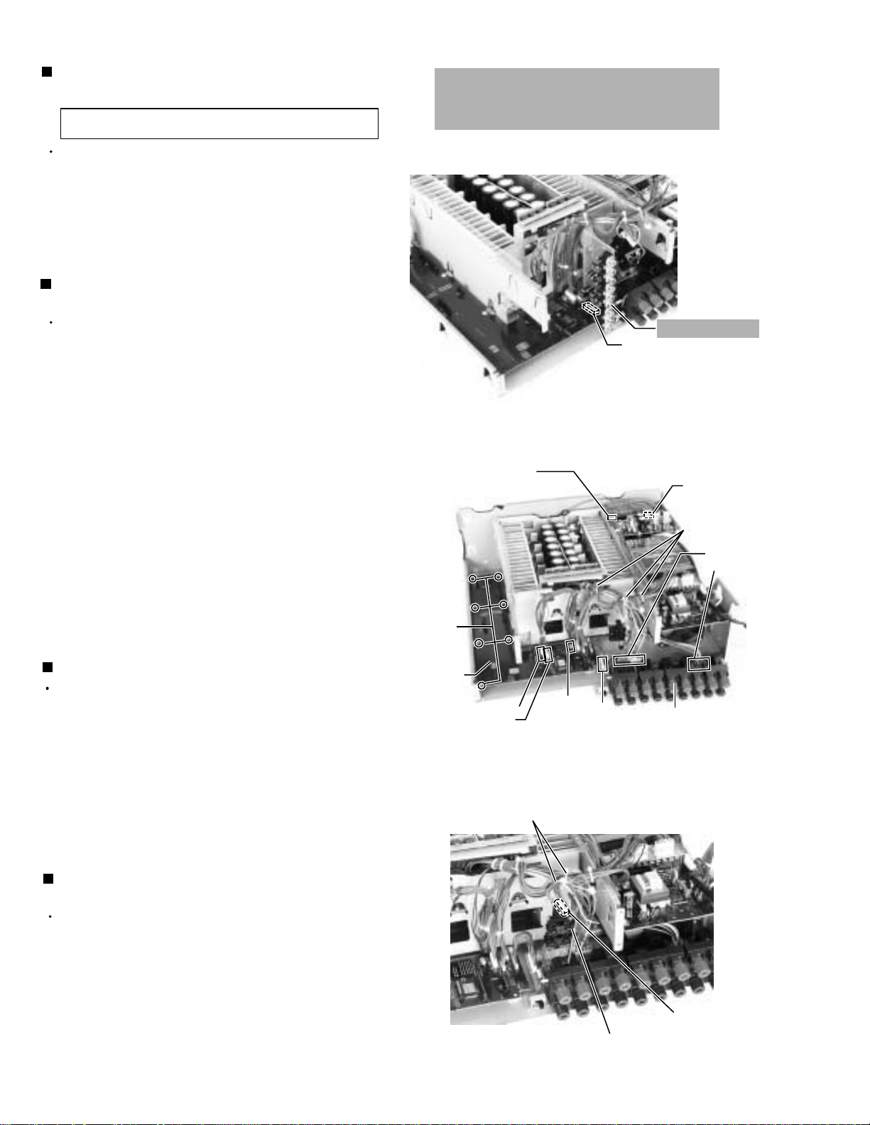
Removing the audio signal 1 board
(See Fig.9)
Prior to performing the following procedure, remove
the top cover, the rear panel and the DSP board.
Disconnect the harness from the connector CN224,
1.
CN207, CN218(J/C only) and CN223 on the audio
signal 1 board.
Removing the plastic rivet.
2.
Disconnect the connector CN206 and CN221 on the
3.
audio signal 1 board.
Removing the audio signal 2 board &
video board & s video board
(See Fig.10 to 12)
Prior to performing the following procedure, remove
the top cover and the rear panel.
1.
Disconnect the harness from connector CN973 on
the front AV in board (see Front panel assembly
section/ fig.2).
2.
Cut off the tie band c.
Plastic rivet
CN224
CN221
CN206
(J/C only)
Tie band c
CN325
(connection to CN15)
CN321
CN207
CN218
CN223
Audio signal 1 board
Fig.9
CN324
WR322
Audio signal
2 board
3.
Disconnect the harness from connector CN324 on
the audio signal 2 board.
4.
Disconnect the connector CN321 and CN325. While
removing the claw of the connector CN15, pull out
the audio signal 2 board.
5.
Cut off the tie band d.
6.
Disconnect the card wire from connector CN402 on
the video board.
7.
Pull out the video board upward.
8.
Cut off the tie band e.
9.
Disconnect the card wire from connector CN432 on
the s video board.
10.
Disconnect the connector CN431 on the s video
board. While removing the claw of the connector
CN8, pull out the s video board.
Fig.10
Tie band d
WR403
CN402
Video board
CN401
Fig.11
Tie band e
WR433
CN432
S video board
CN431
(connection to CN8)
Fig.12
1-7
Page 8
RX-DP10VBK/RX-DP10VSL
RX-DP10RSL
Removing the video SEP board
(See Fig.13)
Note : Video SEP board is not in B/E/EN version.
Prior to performing the following procedures, remove
the top cover and the rear panel.
Disconnect the connector CN501 on the video SEP
1.
board. While removing the claw of the connector
CN9, pull out the video SEP board.
Removing the input base board
(See Fig.14)
Prior to performing the following procedure, remove
the top cover, rear panel, DSP board, audio signal 1
board, audio signal 2 board, video board, s video
board and video SEP board.
Cut off the tie bands fixing the harnesses.
1.
Disconnect the harnesses from the connector CN11,
2.
CN16 and CN17 on the input base board.
Disconnect the harnesses from the connector CN63
3.
on the power supply 1 board and CN42 on the power
supply 2 board.
THE INTRODUCTORY NOTES in Figs :
Gray parts do not correspond to B/E/EN
version.
Video SEP board
CN501
(connection to CN9)
Fig.13
CN42
(on Power
supply 2 board)
CN63
(on Power
supply 1 board)
Tie band
Disconnect the harnesses from the connector CN
4.
743 on the speaker board.
Remove the seven screws H attaching the input
5.
base board.
Removing the speaker board (See Fig.14)
Prior to performing the following procedure, remove
the top cover and rear panel.
Attention :
Speaker board is attached the rear
panel by screws.
1.
Cut off the tie band fixing the harnesses.
2.
Disconnect the harnesses from the connector
CN741, CN742 and CN743 on the speaker board.
Removing the compu link board
(See Fig.15)
Prior to performing the following procedure, remove
the top cover and rear panel.
H
Input base
board
CN17
CN16
CN11
Fig.14
Tie band
CN743
CN741
CN742
Speaker board
Attention :
Compu link board is attached the
rear panel by screws.
Cut off the tie band fixing the harnesses.
1.
Disconnect the harness from the connector CN301
2.
on the compu link board.
1-8
Fig.15
Compu link
CN301
board
Page 9
RX-DP10VBK/RX-DP10VSL
RX-DP10RSL
Removing the power supply 1 board
(See Fig.16)
Prior to performing the following procedure, remove
the top cover.
Cut off the tie band fixing the harnesses.
1.
Disconnect the harnesses from the connector CN61,
2.
CN63, CN64 and CN65 on the power supply 1
board.
Remove the four screws I attaching the power supply
3.
1 board.
Removing the regulator board
(See Fig.17)
Prior to performing the following procedure, remove
the top cover and power supply 1 board.
1.
Disconnect the harness from the connector CN45 on
the regulator board.
2.
Remove the screw J attaching the bracket and
regulator board.
Removing the power transformer 1
(See Fig.17)
Prior to performing the following procedure, remove
the top cover and power supply 1 board.
Disconnect the harnesses from the connector CN41,
1.
CN42 and CN43 on the power supply 2 board and
CN45 on the regulator board.
Remove the four screws K attaching the power
2.
transformer 1.
Removing the power/ fuse board
(See Fig.18)
Prior to performing the following procedure, remove
the top cover.
CN63
CN64
CN65
I
CN61
Tie band
CN43
CN42
Harness band
CN45
Regulator
board
L
(Front side)
Fig.16
(Front side)
Bracket
Fig.17
(fixing the
earth wire)
I
Power supply 1 board
J
K
Power cord
TA1 (black)
TA2 (white)
L
PW23 (red)
PW24 (white)
Power
supply 2
board
CN41
Power
transformer
1
Unsolder the solder points TA1, TA2 and PW21,
1.
PW22, PW23, PW24 on the power/ fuse board.
Remove the four screws L attaching the power/ fuse
2.
board.
Removing the power transformer 2
(See Fig.19)
Prior to performing the following procedure, remove
the top cover and power supply 1 board.
Cut off the tie band fixing the harnesses.
1.
Disconnect the harnesses from the connector CN83
2.
and CN84 on the power trans 2 board.
Unsolder the solder points PW81 and PW82 on the
3.
power supply 1 board.
Remove the four screws M attaching the power
4.
transformer 2.
Power/ fuse board
Power trans
1 board
WR81
(to CN61 of
the power
supply 1 board)
M
CN83
CN84
Fig.18
Power
Power
transformer
transformer
2
2
Fig.19
L
PW21 (blue)
PW22 (brown)
PW81
PW82
M
Power trans
2 board
Tie band
1-9
Page 10
RX-DP10VBK/RX-DP10VSL
RX-DP10RSL
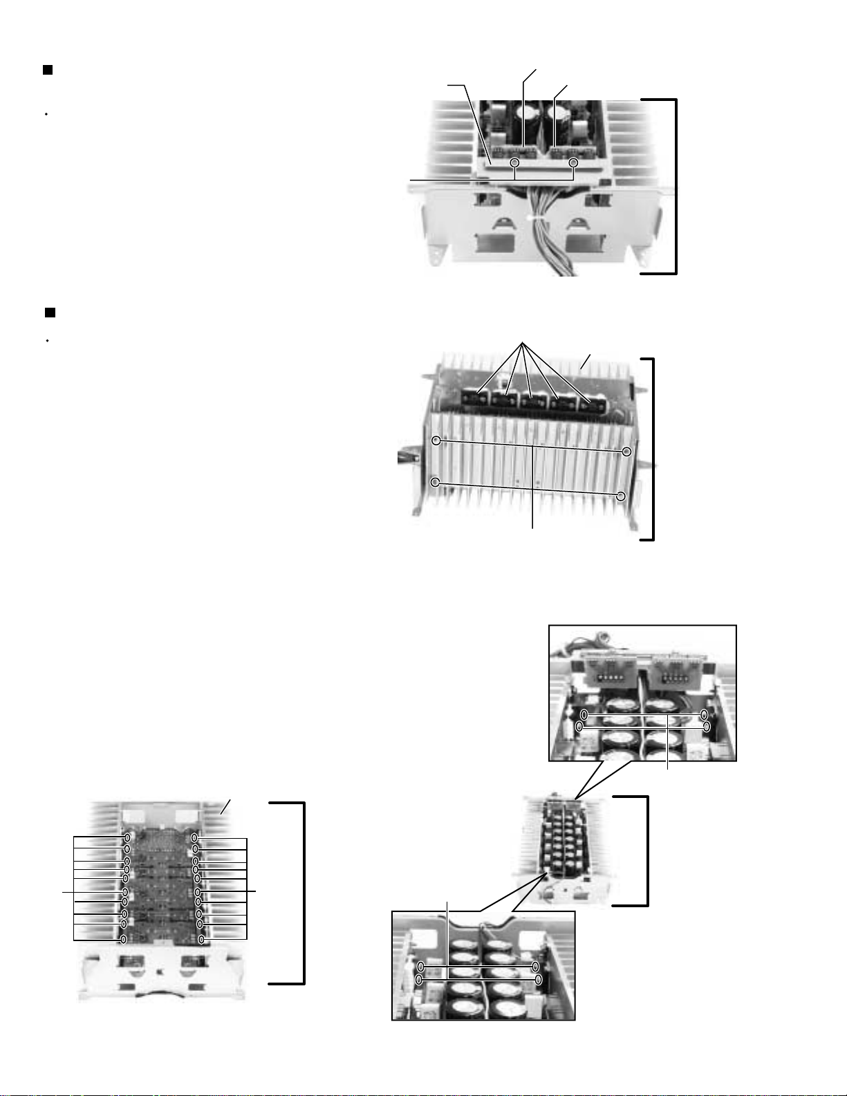
Removing the head phone board
(See Fig.20 and 21)
Prior to performing the following procedures, remove
the top cover, rear panel and front panel assembly.
Disconnect the harnesses from the connector CN981
1.
on the system control board (see fig.5) and CN738
on the power amp. board.
Removing the nut L fixing the head phone board.
2.
Removing the screw M attaching the earth wire and
3.
bracket.
Earth wire
M
Barrier
Bracket
L
Head phone
board
Fig.20
O
Power
amp.
assembly
CN738
Harness band
Removing the power amp. assembly
(See Fig.21 and 22)
Prior to performing the following procedures, remove
the top cover, rear panel, front panel assembly,
system control board, DSP board, shield cover,
audio signal 1 board, audio signal 2 board, video
board, s video board and input base board.
Remove the three screws N fixing the barriers, and
1.
remove the tow barriers.
Remove the eight screws O attaching the power
2.
amp. assembly.
Pull up the power amp. assembly.
3.
N
(Front side)
Fig.21
Barrier
O
Power
amp.
board
O
N
(Rear side)
Fig.22
Removing the fan motor (See Fig.23)
Prior to performing the following procedures, remove
the top cover and rear panel.
Disconnect the harness from the connector CN65 on
1.
the power supply 1 board (see fig.16).
Removing the four screws P attaching the fan motor.
2.
1-10
Fan motor
P
Fig.23
Page 11
<Power amp. assembly section>
Removing the relay board & Rch pre amp.
& Lch pre amp. & center pre amp. &
surround pre amp. (See Fig.1 to 3)
RX-DP10VBK/RX-DP10VSL
RX-DP10RSL
CN70
(on Thermal
compensation
board)
Prior to performing the following procedure, remove
the power amp. assembly.
Cut off the tie band fixing the harnesses.
1.
Disconnect the harness from two connectors CN70
2.
on the thermal compensation board (up side).
Remove the two screws A attaching the relay board.
3.
Disconnect the harness from five connectors CN70
4.
on the thermal compensation board (bottom side).
Pull up Lch pre amp., center pre amp., surround pre
5.
amp. and Rch pre amp. with the relay board from the
power amp. board.
Remove each pre amp. board from the connector
6.
CN721, CN821, CN781 and CN761 on the relay
board.
Harness
band
A
Fig.1
CN761
Tie band
CN781
CN821
CN721
A
Power
amp.
assembly
(up side)
Power
amp.
assembly
(bottom side)
Relay board
Lch
pre amp.
Center
pre amp.
CN723
CN823
Surround
pre amp.
CN783
CN763
Rch
pre amp.
Fig.2
(Front side)
(Rear side)
Fig.3
CN70
(on Thermal
compensation
board)
CN722
CN822
CN782
CN762
Power amp. board
1-11
Page 12
RX-DP10VBK/RX-DP10VSL
RX-DP10RSL
Removing the amp. sub Lo board & amp.
sub Hi board (See Fig.4)
Prior to performing the following procedure, remove
the power amp. assembly.
Remove the two screws B attaching the bracket.1.
Removing the heat sink (See Fig.5 to 7)
Prior to performing the following procedure, remove
the power amp. assembly, relay board, each pre
amp., amp. sub Lo board and amp. sub Hi board.
1.
Remove the eight screws C attaching the heat sink
both side.
2.
Remove the eight screws D attaching the power ICs
(up side).
Bracket
B
Amp. sub Hi board
Amp. sub Lo board
Power
amp.
assembly
(up side)
Fig.4
Power ICs
Heat sink
Power
amp.
assembly
(bottom side)
3.
Remove the twenty screws D attaching the power
ICs (bottom side).
Heat sink
Power
D
D
amp.
assembly
(bottom side)
D
C
(both side)
Fig.5
D
Power
amp.
assembly
(up side)
1-12
Fig.7
Fig.6
Page 13
RX-DP10VBK/RX-DP10VSL
RX-DP10RSL
<Front panel assembly section>
Removing the FL display board & front AV
in board (See Fig.1 and 2)
Prior to performing the following procedure, remove
the top cover and the front panel assembly.
Pull out the volume knob on the front side of the front
1.
panel assembly and remove the nut attaching the FL
display board.
Disconnect the harness from the connector CN973
2.
on the front AV in board.
Remove the three screws A attaching the front AV in
3.
board.
Remove the nine screws B attaching the FL display
4.
board on the back of the front panel.
Disconnect the harnesses from connector CN969,
5.
CN975 and CN982 on the FL display board.
Operation switch panel
Door
Front AV in board
Nut
Volume knob
Fig.1
FL display board
Front panel assembly
CN969
CN975
Removing the power switch board &
motor assembly (See Fig.3)
Prior to performing the following procedure, remove
the front panel assembly and the FL display board.
1.
Remove the four screws C attaching the power
switch board.
2.
Remove the three screws D attaching the motor
assembly on the back of the front panel.
3.
Remove the belt and the two screws a attaching the
motor.
Removing the door input board
(See Fig.3 and 4)
Prior to performing the following procedure, remove
the front panel assembly and the FL display board.
CN973
A
CN982
BB
Fig.2
E
Power switch
board
E
Door
Fig.3
C
D
Belt
Motor assembly
a
Remove the four screws E attaching the door and
1.
remove the door from front panel assembly.
Remove the six screws F attaching the door input
board.
2.
F
Door input board
Door
Fig.4
1-13
Page 14
RX-DP10VBK/RX-DP10VSL
RX-DP10RSL
Adjustment method
Power amplifier section
Adjustment of idling current
/// Measuring point ///
Lch
Rch
Cch
SLch
SRch
SBLch
SBRch
Attention
This adjustment does not obtain a correct adjustment value immediately after the amplifier is
used (state that an internal temperature has risen).
Please adjust immediately after using the amplifier after turning off the power supply of the
amplifier and falling an internal temperature.
<Adjustment method>
Prior to turning the power ON, fully turn the adjusting resistor (VR701, VR702, VR751, VR752, VR771,
1.
VR772, VR801) counterclockwise direction and connect the DC voltmeter to the measuring terminal (B901B902, B903-B904, B905-B906, B907-B908, B909-B910, B911-B912, B913-B914).
Adjust the resistor so that the measured value becomes 2.0mV just after the power supply is turned on.
2.
Adjust the resistor so that the measured value becomes 2.5mV more than 60 seconds after the power supply
3.
is turned on.
After stability is 1.0-4.0mV.
4.
: B903 & B904
: B911 & B912
: B907 & B908
: B905 & B906
: B909 & B910
: B901 & B902
: B913 & B914
/// Alignment point ///
Lch
Rch
Cch
SLch
SRch
SBLch
SBRch
: VR701
: VR751
: VR801
: VR771
: VR772
: VR702
: VR752
*** Measurig condition ***
No load, No signal and Rated line voltage
SURROUND : OFF
Speaker load SW : HIGH (J/C only)
Room temperature : 20~25
The "idling current" graph of the following page is referred to.
* It is not abnormal though the idling current might not become 0mA even if it is finished to turn variable
resistance (VR701, VR702, VR751, VR752, VR771, VR772, VR801) in the direction of counterclockwise.
Heat sink
B901, B902 (SBLch)
B903, B904 (Lch)
VR701 (Lch)
VR702 (SBLch)
VR801 (Cch)
VR771 (SLch)
VR751 (Rch)
B905, B906 (SLch)
B907, B908 (Cch)
VR772 (SRch)
B909, B910 (SRch)
VR752 (SBRch)
B911, B912 (Rch)
1-14
B913, B914 (SBRch)
Page 15
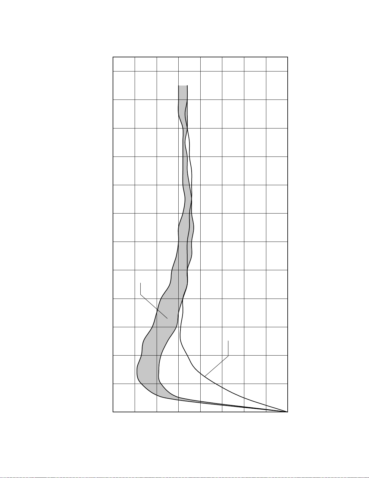
RX-DP10VBK/RX-DP10VSL
RX-DP10RSL
Time (min)
Channels other than a center channel are this zone.
RX-DP10 Idling Current
4
3.5
Center channele
1 2 3 4 5 6 7 8 9 10
3
2.5
2
1.5
1
0.5
0
Voltage at measering point (mV)
1-15
Page 16
RX-DP10VBK/RX-DP10VSL
RX-DP10RSL
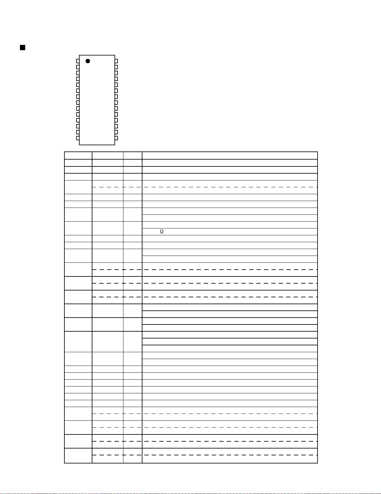
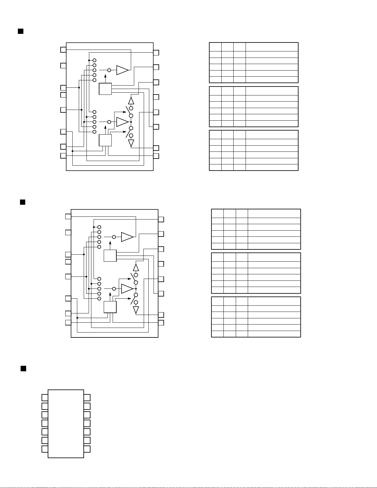
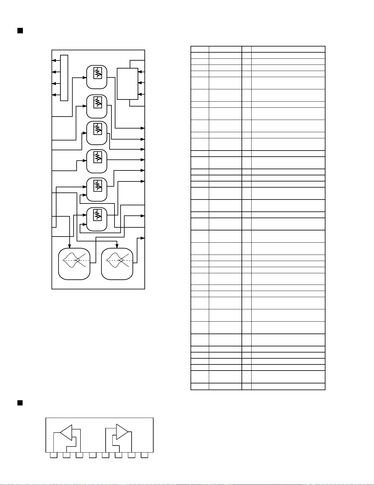
Description of major ICs
AK4112 (IC673) : Digital audio receiver
1.Pin layout
DVDD
DVSS
TVDD
V/TX
XTI
XTO
PDN
AVDD
AVSS
RX1
RX2/DIF0
RX3/DIF1
RX4/DIF2
1
2
3
4
5
6
7
8
R
9
10
11
12
13
14
28
CM0/CDTO
27
CM1/CDT1
26
OCKS1/CCLK
25
OCKS0/CSN
24
MCKO1
23
MCKO2
22
DAUX
21
BICK
20
SDTO
19
LRCK
18
ERF
17
FS96
16
P/SN
15
AUTO
2.Pin function
Pin No.
1
2
3
4
5
6
7
Symbol
DVDD
DVSS
TVDD
V
TX
XTI
XTO
PDN
I/O
Digital Power Supply Pin, 3.3V
Digital Ground Pin
Input Buffer Power Supply Pin, 3.3V or 5V
Validity Flag Output Pin in Parallel Mode
O
Transmit channel (through data) Output Pin in Serial Mode
O
X'tal Input Pin
I
X'tal Output Pin
O
Power-Down Mode PIn
I
Function
When "L", the AK4112A is powered-down and reset.
8
R
External Resistor Pin
18k +/-1% resistor to AVSS externally.
9
10
11
AVDD
AVSS
RX1
Analog Power Supply Pin
Analog Ground Pin
Receiver Channel 1
I
This channel is selected in Parallel Mode or default of Serial Mode.
12
13
14
15
DIF0
RX2
DIF1
RX3
DIF2
RX4
AUTO
Audio Data Interface Format 0Pin in Parallel Mode
I
Receiver Channel 2 in Serial Mode
I
Audio Data Interface Format 1 Pin in Parallel Mode
I
Receiver Channel 3 in Serial Mode
I
Audio Data Interface Format 2 Pin in Parallel Mode
I
Receiver Channel 4 in Serial Mode
I
Non-PCM Detect Pin
O
"L": No detect, "H": Detect
16
P/S
Parallel/Serial Select Pin
I
"L": Serial Mode, "H": Parallel Mode
17
FS96
96kHz Sampling Detect Pin
O
(RX Mode) "H": fs=88.2kHz or more, "L": fs=54kHz or less.
(X'tal Mode) "H": XFS96=1, "L": XFS96=0.
18
ERF
Unlock & Parity Error Output Pin
O
"L": No Error, "H": Error
19
20
21
22
23
24
25
26
27
28
LRCK
SDTO
BICK
DAUX
MCK02
MCK01
OCKS0
CSN
OCKS1
CCLK
CM1
CDTI
CM0
CDTO
Output Channel Clock Pin
I/O
Audio Serial Data Output Pin
O
Audio Serial Data Clock Pin
I/O
Auxiliary Audio Data Input Pin
I
Master Clock #2 Output Pin
O
Master Clock #1 Output Pin
O
Output Clock Select 0 Pin in Parallel Mode
I
Chip Select Pin in Serial Mode
I
Output Clock Select 1 Pin in Parallel Mode
I
Control Data Clock Pin in Serial Mode
I
Master Clock Operation Mode Pin0 in Parallel Mode
I
Control Data Input Pin in Serial Mode
I
Master Clock Operation Mode Pin1 in Parallel Mode
I
Control Data Output Pin in Serial Mode
O
Note 1: All input pins except internal pull-down pins should not be left floating.
1-16
Page 17
3.Block diagram
AVSS
AVDD R MCKO1 MCKO2 XTI XTO
RX-DP10VBK/RX-DP10VSL
RX-DP10RSL
RX1
RX2
RX3
RX4
V/TX
DVDD
DVSS
PDN
Input
Selector
System
Control
Clock
Recovery
DAIF
Decoder
AC-3/MPEG
Detect
AUTO ERF P/S="L"
Clock
Generator
DEM
Error
Detect
X'tal
Oscillator
Serial Control Mode
96kHz
Detect
Audio
I/F
p I/F
FS96
DAUX
LRCK
BICK
SDTO
TVDD
CSN
CCLK
CDTO
CDTI
RX1
V
DVDD
DVSS
OCKS0
OCKS1
CM0
CM1
PDN
System
Control
AVSS
AVDD R MCKO1 MCKO2 XTI XTO
Clock
Recovery
DAIF
Decoder
AC-3/MPEG
Detect
AUTO ERF P/S="H"
Clock
Generator
DEM
Error
Detect
Parallel Control Mode
X'tal
Oscillator
4
96kHz
Detect
Audio
I/F
FS96
DAUX
LRCK
BICK
SDTO
DIF0
DIF1
DIF2
TVDD
OCKS0
OCKS1
CM0
CM1
1-17
Page 18
RX-DP10VBK/RX-DP10VSL
RX-DP10RSL
AK5383VF (IC657) : A/D converter
1. Pin layout
VREFR
VRFEL
GNDL
VCOML
AINL+
DGND
SMODW2
SMODE1
LRCK
SCLK
2. Block diagram
VREFL
GNDL
VCOML
AINL+
AINLZCAL
AINR+
AINR-
VCOMR
VREFR
GNDR
1
2
3
4
5
6
25
24
26
28
27
23 22 21 9 10 7 8
AINLZCAL
VD
CAL
RST
Voltge
Reference
Delta-Sigma
Mdulator
Delta-Sigma
Mdulator
Voltge
Reference
1
2
3
4
5
6
7
8
9
10
11
12
13
14
28
GNDR
27
VCOMR
26
AINR+
25
AINR-
24
VA
23
AGND
22
BGND
21
TEST
20
HPFE
19
DFS
18
MCLK
17
FSYNC
16
SDATA
15
SMODE1 SMODE2 SLCK LRCK FSYNC
12 11 14 13 16
Serial Output
Interface
Decimation
Filter
Decimation
Filter
Controller
HPF
HPF
Calibration
SRAM
15
19
17
18
SDATA
HPFE
MCLK
DFS
VA AGND BGND CAL RST VD DGND
3. Pin function (1/2)
Pin No.
1
Pin name
VRFEL
I/O
Function
O
Lch Reference Voltage Pin, 3.75V
Normally connected to GNDL with a 10 F electrolytic capacitor and
a 0.1 F ceramic capacitor.
2
3
4
5
6
GNDL
VCOML
AINL+
AINLZCAL
-
Lch Reference Ground Pin, 0V
O
Lch Common Voltage Pin, 2.75V
I
Lch Analog positive input Pin
I
Lch Analog negative input Pin
I
Zero Calibration Control Pin
This pin controls the calibration reference signal.
"L": VCOML and VCOMR
"H": Analog Input Pins (AINL , AINR )
7
8
VD
DGND
-
Digital Power Supply Pin, 3.3V
-
Digital Ground Pin, 0V
1-18
Page 19
RX-DP10VBK/RX-DP10VSL
RX-DP10RSL
3. Pin function (2/2)
Pin No.
9
10
11
12
Pin name
CAL
RST
SMODE2
SMODE1
I/O
Function
O
Calibration Active Signal Pin
"H" means the offset calibration cycle is in progress. Offset calibration starts
when RST goes "H". CAL goes "L" after 8704 LRCK cycles for DFS="L",
17408 LRCK cycles for DFS="H".
I
Reset Pin
When "L", Digital section is powered-down. Upon returning "H", an
offset calibration cycle is started. An offset calibration cycle should always
be initiated after power-up.
I
Serial Interface Mode Select Pin
I
MSB first, 2's compliment.
SMODE2
L
L
H
H
SMODE1
L
H
L
H
MODE
Slave mode : MSB justified
Master mode : Similar to I2S
Slave mode :I2S
Master mode : I2S
LRCK
: H/L
: H/L
: L/H
: L/H
13
14
15
16
17
18
19
20
21
22
23
24
25
26
27
28
LRCK
SCLK
SDATA
FSYNC
MCLK
DFS
HPFE
TEST
BGND
AGND
VA
AINR-
AINR+
VCOMR
GNDR
VREFR
I/O
Left/Right Channel Select Clock Pin
LRCK goes "H" at SMODE2="L" and "L" at SMODE2="H" during reset
when SMODE1 "H".
I/O
Serial Data Clock Pin
Data is clocked out on the falling edge of SCLK.
Slave mode:
SCLK requires more than 48fs clock.
Master mode:
SCLK outputs a 128fs(DFS="L") or 64fs (DFS="H")clock.
SCLK stays "L" during reset.
O
Serial Data Output Pin
MSB first, 2's complement. SDATA stays "L" during reset.
I/O
Frame Synchronization Signal Pin
Slave mode:
When "H", the data bits are clocked out on SDATA. In I2S mode, FSYNC is
Don't care.
Master mode:
FSYNC outputs 2fs clock. FSYNC stays "L" during reset.
I
Master Clock Input Pin
256fs at DFS="L", 128fs at DFS="H".
I
Double Speed Sampling mode Pin
"L": Normal Speed "H": Double Speed
I
High Pass Filter Enable Pin
"L": Disable "H": Enable
I
Test Pin (pull-down pin)
Should be connected to GND.
-
Substrate Ground Pin, 0V
-
Analog Ground Pin, 0V
-
Analog Supply Pin, 5V
I
Rch Analog negative input Pin
I
Rch Analog positive input Pin
O
Rch Common Voltage Pin, 2.75V
-
Rch Reference Ground Pin, 0V
O
Rch Reference Voltage Pin, 3.75V
Normally connected to GNDR with a 10 F electrolytic capacitor and a 0.1 F
ceramic capacitor
Note: All digital inputs should not be left floating.
1-19
Page 20
RX-DP10VBK/RX-DP10VSL
RX-DP10RSL
JCV8006 (IC635, IC640, IC645, IC650) : CC converter
1. Pin layout
VSS
TOUT0
TOUT1
TOUT2
DOUT1
BCKO1
WCKO1
VDD
VSS
DOUT2
BCKO2
WCKO2
TOUT3
TOUT4
TOUT5
VDD
VDD
FP1
FP2
WSN
WS
RAMT
VSS
CLK
VDD
DFR1
DFR2
DF1
DF2
DFSEL
SH
VSS
484746454443424140393837363534
49
50
51
52
53
54
55
56
57
58
59
60
61
62
63
64
123456789101112131415
VDD
VCK
DIN
LRCK
CAD1
CAD0
VSS
RESET
MODE
MDT/IW1N
MCK/IW2N
MLEN/IOF
BT
D1W1
D1W2
33
32
31
30
29
28
27
26
25
24
23
22
21
20
19
18
17
16
VSS
VSS
TOUT6
TOUT7
TOUT8
TOUT9
TOUTA
TOUTD
VDD
TMD0
TMD1
CKSLN
PDN
CKDV
F192
TSTEN
VDD
2. Pin function (1/2)
Pin No.
l=CMOS, l1=Schmitt, lp2=Schmitt with pull-down resistor, O=CMOS (H=VDD, L=VSS)
1
2
3
4
5
6
7
8
9
10
11
12
13
14
15
16
17
18
19
20
Pin name
VDD
BCK
DIN
LRCK
CAD1
CAD0
RESET
VSS
MODE
MCK/IW2N
MDT/IW1N
MLEN/IOF
BTR
D1W1
D1W2
VSS
VDD
TSTEN
F192
CKDV
Function
I/O
-
Power supply : All VDD pins must be connected externally
l1
Bit clock input :Bit click if serial data into the DIN ; Must run continuously, "5V tolerant"
l1
Serial audio data input, "5V tolerant"
l1
Left/Right clock input ; sampling frequency (fs) for DIN ; Must run continuously, "5V tolerant"
lp2
Chip address 1 ; available on MODE=H
lp2
Chip address 0 ; available on MODE=H
l1
System reset ; the internal state is reset to the default setting when L, "5V tolerant"
-
Ground ; All VSS pins must be connected externally
lp2
System control mode select input : (H=Software mode ; L=Hardware mode)
l1
Control clock input ; MODE=H,
/Select input audio data word length input2 ; MODE=L, "5V tolerant"
l1
Control data input ; MODE=H,
/Select input audio data word length input 1 ; MODE=L, "5V tolerant"
l1
Control data latch input ; MODE=H,
/select input and output audio data format input ; MODE=L, "5V tolerant"
lp2
Select BIT-UP through mode input ; MODE=L
lp2
Select output 1 audio data word length and enable control 1 ; MODE=L
lp2
Select output 1 audio data word length and enable control 2 ; MODE=L
-
Ground ; All VSS pins must be connected externally
-
Power supply ; All VSS pins must be connected externally
lp2
Test control input ; in normal operation this pin should be terminated to ground
lp2
Select system clock for 192kHz input sampling frequency input : MODE=L,
(supported for FS-UP only)
lp2
Internal click divider select input ; MODE=L,(L=1, H=1/2)
1-20
Page 21

RX-DP10VBK/RX-DP10VSL
RX-DP10RSL
2. Pin function (2/2)
Pin No.
21
22
23
24
25
26
27
28
29
30
31
32
33
34
35
36
37
38
39
40
41
42
43
44
45
46
47
48
49
50
51
52
53
54
55
56
57
58
59
60
61
62
63
64
Pin name
PDN
CKSLN
TMD1
TMD0
VDD
TOUTD
TOUTA
TOUT9
TOUT8
TOUT7
TOUT6
VSS
VDD
TOUT5
TOUT4
TOUT3
WCKO2
BCKO2
DOUT2
VSS
VDD
WCKO1
BCKO1
DOUT1
TOUT2
TOUT1
TOUT0
VSS
VDD
FP1
FP2
WSN
WS
RAMT
VSS
CLK
VDD
DFR1
DFR2
DF1
DF2
DFSEL
SH
VSS
I/O
lp2
lp2
lp2
lp2
O
O
O
O
O
O
-
O
O
O
O
O
O
-
O
O
O
O
O
O
-
-
lp2
lp2
lp2
lp2
lp2
-
-
lp2
lp2
lp2
lp2
lp2
lp2
-
Function
Power down control input ; MODE=L, (L=normal, H=power down)
System clock select input ; MODE=L, (L=512fs, H=384fs)
Test input ; in normal operation this pin should be terminated to ground
Test input ; in normal operation this pin should be terminated to ground
Power supply ; All VDD pins must be connected externally
Test output ; this pin should be left open
Test output ; this pin should be left open
Test output ; this pin should be left open
Test output ; this pin should be left open
Test output ; this pin should be left open
Test output ; this pin should be left open
Ground ; All VSS pins must be connected externally
Power supply ; All VDD pins must be connected externally
Test output ; this pin should be left open
Test output ; this pin should be left open
Test output ; this pin should be left open
L/R clock output 2 ; the left or right channel for the DOUT2
Bit clock output 2 ; bit clock of serial data for the DOUT2
Serial audio data output 2
Ground ; All VSS pins must be connected externally
Power supply ; All VDD pins must be connected externally
L/R clock output 1 ; the left or right channel for the DOUT 1
Bit clock output 1; bit clock of serial data for the DOUT1
Serial audio output 1
Test output ; this pin should be left open
Test output ; this pin should be left open
Test output ; this pin should be left open
Ground ; All VSS pins must be connected externally
Power supply ; All VDD pins must be connected externally
Select FS-UP peak data compensation coefficient input 1 ; MODE=L
Select FS-UP peak data compensation coefficient input 2 ; MODE=L
Select FS-UP waveform compensation function control for 16fd to 9fd input ; MODE=L
Select FS-UP waveform compensation function control for 8fd to 2fd input ; MODE=L
RAM test control input ; in normal operation this pin should be terminated to ground
Ground ; All VSS pins must be connected externally
l
Master clock input ; Must run continuously normal operation, "5V tolerant"
Power supply ; All VDD pins must be connected externally
Select DF over sampling rate control 1 input for FS-UP and output 2 ; MODE=L
Select DF over sampling rate control 2 input for FS-UP and output 2 ; MODE=L
Select DF over sampling rate control 1 input for output 1 ; MODE=L
Select DF over sampling rate control 2 input for output 1 ; MODE=L
Select DF internal digital fitter ; MODE=L, (L=84tap FIR, H=169tap FIR)
Select SH mode control input ; MODE=L, (L=ON, H=OFF)
Ground ; All VSS pins must be connected externally
l=CMOS, l1=Schmitt, lp2=Schmitt with pull-down resistor, O=CMOS (H=VDD, L=VSS)
1-21
Page 22
RX-DP10VBK/RX-DP10VSL
RX-DP10RSL
XCA56367PV150 (IC661, IC666) : DSP
1. Pin layout
MISO/SDA
144
HREQ#
VCCS
GNDS
FST
FSR
SCKT
SCKR
HCKT
HCKR
VCCQL
GNDQ
VCCQH
VCCS
GNDS
ADO
ACI
TIO0
HAD7
HAD6
HAD5
1
2
3
4
5
6
7
8
9
10
11
12
13
14
15
16
17
18
19
20
21
22
23
24
25
26
27
28
29
30
31
32
33
34
35
36
3738394041424344454647484950515253545556575859606162636465666768697071
HAD4
2. Block diagram
SCK/SCL
SS#/HA2
SDO0/SDO0_1
SDO2/SDI3/SDO2_1/SDI3_1
SDO3/SDI2/SDO3_1/SDI2_1
SDO1/SDO1_1
SDO4/SDI1
SDO5/SDI0
HDS/HWR
HRW/HRD
HACK/HRRQ
HOREQ/HTRQ
HCS/HA10
HA9/HA2
HA8/HA1
HAS/HA0
MOSI/HA0
TMS
TCK
143
142
141
HAD3
VCCH
GNDH
TDI
TDO
SDO4_1/SDI1_1
MODA/IRQA#
140
139
138
137
HAD2
HAD1
HAD0
RESET#
MODB/IRQB#
MODCIRQC#
MODD/IRQD#
D23
D22
136
135
134
133
132
PCAP
VCCP
GNDP
VCCQH
SDO5_1/SDI0_1
D21
GNDD
131
130
AA2
FST_1
VCCD
D20
129
128
CAS#
SCKT_1
GNDQ
VCCQL
127
126
GNDQ
EXTAL
D19
D18
125
124
VCCC
VCCQL
D17
D16
123
122
GNDC
FSR_1
D15
GNDD
121
120
SCKR_1
PINT/NMI#
VCCD
D14
119
118
TA#
BR#
D13
117
BB#
D12
116
VCCC
D11
115
GNDC
D10D9GNDD
VCCDD8D7
114
113
112
111
AA1
AA0
RD#
WR#
110
BG#
109
108
107
106
105
104
103
102
101
100
D6
D5
D4
D3
GNDD
VCCD
D2
D1
D0
A17
99
A16
98
A15
97
GNDA
96
VCCQH
95
A14
94
A13
93
A12
92
VCCQL
91
GNDQ
90
A11
89
A10
88
GNDA
87
VCCA
86
A9
85
A8
84
A7
83
A6
82
GNDA
81
VCCA
80
A5
79
A4
78
A3
77
A2
76
GNDA
75
VCCA
74
A1
73
72
A0
1-22
12168465
TRIPLE
TIMER
DAX
(SPDIFx.)
INTERFACE
HOST
INTERFACE
ESAI
INTERFACE
SHI
INTERFACE
ESAI_1
PERIPHERAL
EXPANSION AREA
ADDRESS
GENERATION
UNIT
SIX CHANNELS
DMA UNIT
24-BIT
DSP56300
Core
INTERNAL
DATA
BUS
PLL
CLOCK
GENARAT
EXTAL
RESET
PINIT/NMI
PROGRAM
INTERRUPT
CONTROLLER
PROGRAM
DECODE
CONTROLLE
MODA/IRQA
MODB/IRQB
MODC/IRQC
MODD/IRQD
PROGRAM
ADDRESS
GENERATOR
MENORY EXPANTION AREA
PROGRAM
RAM
/INSTR
CACHE
3Kx24
Bootstrap
X MEMORY
RAM
13K x 24
ROM
32K x 24
PM_EB XM_EB YM_EB
YAB
XAB
PAB
DAB
DDB
YDB
XDB
PDB
GDB
DATA ALU
24 x 24 + 56->56-BIT MAC
TWO 56-BIT ACCUMULATORS
BARREL SHIFTER
24BITS BUS
Y MEMORY
RAM
7K x 24
ROM
8K x 24
EXTERNAL
ADDRESS
SRAM BUS
INTERGACE
EXTERNAL
DATA BUS
BUS
SWITCH
DRAM &
&
I-CACHE
SWITCH
POWER
MNGMNT
JTAG
OnCE
18
ADDRESS
10
CONTROL
24
DATA
4
Page 23
3. Signal groupings
RX-DP10VBK/RX-DP10VSL
RX-DP10RSL
PORT A ADDRESS BUS
A0-A17
VCCA(3)
GNDA(4)
PORT A DATA BUS
D0-D23
VCCS(4)
GNDD(4)
PORT A BUS CONTROL
AA0-AA2/RAS0-RAS2
CAS
RD
WR
TA
BR
BG
BB
VCCC(2)
GNDC(2)
INTERRUPT AND
MODEL CONTROL
MODA/IRQA
MODB/IRQB
MODC/IRQC
MODD/IRQD
RESET
PLL AND CLOCK
EXTAL
PINIT/NMI
PCAP
VCCP
GNDP
QUIET POWER
VCCQH(3)
VCCQL(4)
GNDQ(4)
Port B
Port C
Port E
OnCE ON-CHIP EMULATION/JTAG PORT
TDI
TCK
TDO
TMS
PARALLEL HOST PORT(HD108)
HAD(7:0)[PB0-PB7]
HAS/HA0[PB8]
HA8/HA1[PB9]
HA9/HA2[PB10]
HRW/HRD[PB11]
HCS/HA10[PB13]
HOREQ/HTRQ[PB14]
HACK/HRRQ[PB15]
VCGH
GNDH
SERIAL AUDIO INTERFACE (ESAI)
SCKT[PC3]
FST[PC4]
HCKT[PC5]
SCKR[PC0]
FSR[PC1]
HCKR[PC2]
SDO0[PC11]/SDO0_1[PE11]
SDO1[PC10]/SDO1_1[PE10]
SDO2/SDI3]PC9]/SDO2_1/DSI3_1[PE9]
SDO3/SDI2[PC8]/SDO3_1/DSI2_1[PE8]
SDO4/SDI1[PC7]
SDO5/SDI0[PC6]
SERIAL AUDIO INTERFACE (ESAI_1)
SCKT_1[PE3]
FST_1[PE4]
SCKR_1[PE0]
FSR_1[PE7]
SDO4_1/SDI1_1[PE7]
SDO5_1/SDI0_1[PE6]
VCCS(2)
GNDS(2)
SPDIF TRANSMITTER(DAX)
ADO[PD1]
ACI[PD0]
TIMER 0
RIO0[TIO0]
Port D
SERIAL HOST INTERFACE (SHI)
MOSI/HA0
SS/HA2
MISO/SDA
SCK/SCL
HREQ
1-23
Page 24
RX-DP10VBK/RX-DP10VSL
RX-DP10RSL
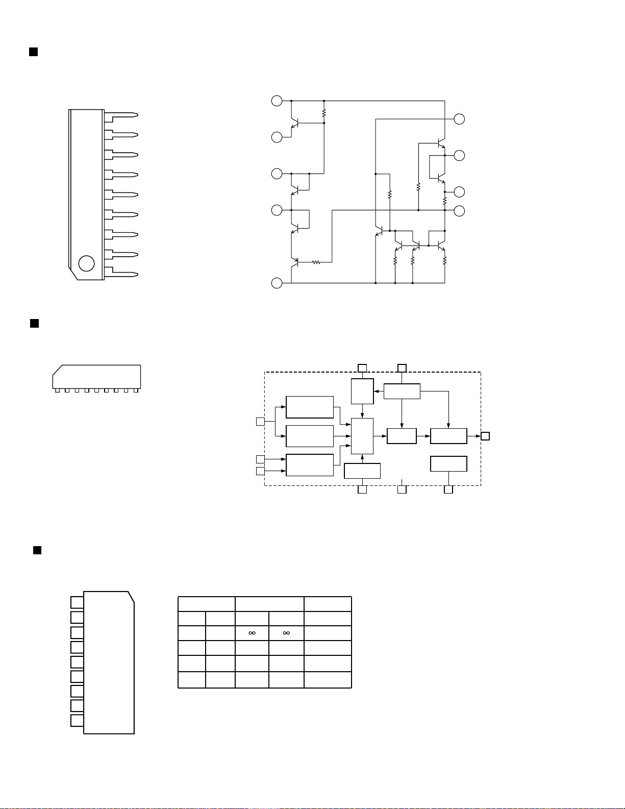
BA7625 (IC401, IC431, IC451, IC471) : Video selector
MONITOR OUT
GND
IN5
GND
IN4
CTL E
IN3
CTL D
1
2
3
4
5
6
7
8
6dB
logic
6dB
logic
16
15
14
13
12
11
10
11
BA7626 (IC472, IC732) : Video selector
MONITOR OUT
GND
IN5
GND
IN4
CTL E
IN3
CTL D
1
2
3
4
5
6
7
8
6dB
logic
6dB
logic
IN1
CTL A
VOUT 1
CC
V
IN2
CTL B
VOUT 2
CTL C
16
15
14
13
12
11
10
11
IN1
CTL A
VOUT 1
CC
V
IN2
CTL B
VOUT 2
CTL C
A B E MONITOR OUT
LL
HL
LH
H H L IN4
*
*
*
H H H IN5
IN1
IN2
IN3
C D E VOUT1
LL
HL
LH
H H L IN4
*
*
*
H H H IN5
-IN2
IN3
C D E VOUT2
LL
HL
LH
H H L IN4
*
*
*
H H H IN5
IN1
-IN3
A B E MONITOR OUT
LL
HL
LH
H H L IN4
*
*
*
H H H IN5
IN1
IN2
IN3
C D E VOUT1
LL
HL
LH
H H L IN4
*
*
*
H H H IN5
-IN2
IN3
C D E VOUT2
LL
HL
LH
H H L IN4
*
*
*
H H H IN5
IN1
-IN3
MAX4018ESD (IC503, IC544) : Op. amp.
1-24
ENA
ENC
ENB
Vcc
INA+
INA-
OUTA
1
2
3
4
5
6
7
14
13
12
11
10
OUTC
INCINC+
V
EE
INB+
INB-
9
OUTB
8
Page 25
BU4051BC (IC461) : Analog multiplexer/ DE multiplexer
RX-DP10VBK/RX-DP10VSL
RX-DP10RSL
1. Pin layout
1
X4
2
X6
3
X
4
X7
5
X5
6
INH
7
VEE
8
VSS
VDD16
X215
X114
X013
X312
A11
B10
C9
2. Block diagram
16
VDD
6
INH
11
A
10
B
9
C
8
VSS
7
VEE
13
X0
14
X1
15
X2
12
X3
1
X4
5
X5
2
X6
4
X7
NJM2285V (IC402, IC452) : Video switch
1. Block diagram
GND 1 IN 2B
IN A
16 15 14 13 12 11 10 9
CTL 2 IN 2A GND 3 IN 3B
V+
LEVEL
CONVERTER
BINARY TO 1 OF 8
DECODER WITH INHIBIT
3X
HL
L
H
Bias Type
Clamp Type
Clamp Type
H
L
12345678
IN 1B
CTL 1
OUT 1
GND 2 OUT 2
OUT 3 CT L3 IN 3A
NJM4580E (IC201, 204, 241, 242, 251, 252, 253, 254, 261, 263, 271, 272, 273, 281, 631,
632, 633, 636, 637, 638, 641, 642, 643, 646, 647, 648, 655, 656, 686, 687) : L.P.F.
A OUT
A -IN
A +IN
V-
1
2
A
B
3
4
8
7
6
5
V+
B OUT
B -IN
B +IN
(TOP VIEW)
1-25
Page 26
RX-DP10VBK/RX-DP10VSL
RX-DP10RSL
M62446FP (IC653) : 6CH master volume
1.Block diagram
SWin
SRin
SLin
Cin
Rin
Lin
LTRE
10
11
12
13
14
15
16
17
18
19
20
21
1
2
MCU
3
4
OUTPUT PORT
volume
I/F
5
6
volume
7
8
volume
9
volume
volume
volume
tone
tone
OUT4
OUT3
OUT2
OUT1
AVDD
GNDS
GNDC
GNDR
GNDL
BYPASSR
BYPASSL
LBASS3
LBASS2
LBASS1
42
41
40
39
38
37
36
35
34
33
32
31
30
29
28
27
26
25
24
23
22
DVDD
CLK
DA TA
LATCH
DGND
AGND
SWout
SRout
SLout
Cout
Rout
Lout
AVSS
CL1
CL2
CR1
CR2
RTRE
RBASS3
RBASS2
RBASS1
2. Pin functions
Pin No.
1
2
3
4
5
6
7
8
9
10
11
12
13
14
15
16,17
18
19~21
22
23,24
25
26
27
28
29
30
31
32
33
34
35
36
37
38
39
40
41
42
Symbol
OUT 4
OUT 3
OUT 2
OUT 1
AVDD
SWin
A.GND
SR in
SL in
A.GND
C in
A.GND
R in
A.GND
L in
AVSS
L out
R out
C out
SL out
SR out
SW out
A.GND
D.GND
LATCH
VOL DATA
VOL CLK
DVDD
I/O
Descriptions
O
PORT output
O
PORT output
O
PORT output
O
PORT output
-
Analog positive power supply
terminal
I
SUB Woofer ch volume signal
input terminal
-
Analog ground terminal
I
SR ch volume signal input
terminal
I
SL ch volume signal input
terminal
-
Analog ground terminal
I
Center ch volume signal input
terminal
-
Analog ground terminal
I
R ch volume signal input
terminal
-
Analog ground terminal
I
L ch volume signal input terminal
-
Non connect
-
Frequency adjustment terminal
tone/treble
-
Frequency adjustment terminal
tone/bass
O
Tone output terminal
-
Frequency adjustment terminal
tone/bass
-
Frequency adjustment terminal
tone/treble
-
Frequency adjustment terminal
tone/bass
I
L/R volume input terminal
O
Tone output terminal
I
L/R volume input terminal
-
Analog negative power supply
terminal
O
L ch output
O
R ch output
O
Center ch volume signal output
terminal
O
SL ch volume signal output
terminal
O
SR ch volume signal output
terminal
O
SUB Woofer ch volume signal
output terminal
-
Analog ground terminal
-
Digital ground terminal
I
Latch input terminal
I
Volume data input terminal
I
Clock input terminal
for data transfer
-
Digital power supply terminal
BA15218N (IC381, IC382) : Dual op. amp.
+
2
-
1-26
+
1
-
1 2 3 4 5 6 7 8
OUT1 -IN1 +IN1
+IN2 -IN2 OUT2
GND
Vcc
Page 27
NJM2903M (IC282, IC998) : Temperature detector
1. Pin layout
+
V
A OUTPUT
1
8
RX-DP10VBK/RX-DP10VSL
RX-DP10RSL
A -INPUT
A +INPUT
GND
2. Block diagram
+
V
+INPUT
-INPUT
D101
2
3
4
Q110
Q101
(TOP VIEW)
Q109
D103
Q103
Q104
Q111
D104
Q102
D102
7
6
5
Q112
Q107
B OUTPUT
B -INPUT
B +INPUT
Q108
Q5
Q8
Q4
Q7
Q1
Q3
R1
Q105
Q106
GND
PQ20VZ11 (IC690) : Regulator
1. Pin layout 2. Block diagram
1 3
Vin
1 2 3 4 5
Vc Vadj
2
OUTPUT
IC
5
GND
Q6
Q2
Vo
4
1-27
Page 28
RX-DP10VBK/RX-DP10VSL
RX-DP10RSL
VC5022-2 (IC601, IC603, IC605, IC606, IC607) : Advanced super A
1. Pin layout 2. Block diagram
1
R1
Q1
2
9
Q10
8
19
TA7317P (IC951) : Protecter
1.Pin layout
1 92 3 4 5 6 7 8
2.Block diagram
PowerON/OFF
OverCurrent
DC Detect
1
2
3
3
4
Q4
5
Power ON/OFF
Detector
Over Current
Detector
DC Voltage
Detector
Q2
Q3
R2
R8
R3
Q5
Q6 Q7
R4
R4 R6
V
Muting IN
8
Muting
Circuit
OR
Circuit
Discharge
7 4 5
Dis chaerge
CC
9
Regulator
Schmitt
GND
Q9
R7
Relay Drive
Substrate
Substrate
Q8
7
6
Relay
6
Output drive
TA8409S (IC967) : Motor driver
1.Pin layout
1
IN2
2
VCC
3
OUT 2
4
GND
5
GND
6
VS
7
OUT 1
8
VR
9
IN1
1-28
TA8409S
2. Truth table
INPUT OUTPUT MODE
IN1
IN2
OUT1
0
0
1
0
0
1
1
1
OUT2
H
L
L
L
H
L
MOTOR
STOP
CW/CCW
CCW/CW
BRAKE
Page 29
SAA6588 (IC311) : RDS detector
RX-DP10VBK/RX-DP10VSL
RX-DP10RSL
1.Pin layout
MRO
NC
GND
OSCO
OSCI
VSSD
VDDD
DAVN
SDA
SCL
1
2
3
4
5
6
7
8
9
10
20
19
18
17
16
15
14
13
12
11
NC
CIN
SCOUT
Vref
MPX
VSSA
VDDA
NC
GND
NC
2.Pin function
Pin
No.
1
2
3
4
5
6
7
8
9
10
11
12
13
14
15
16
17
18
19
20
MRO
NC
GND
OSCO
OSCI
VSSD
VDDD
DAVN
SDA
SCL
NC
GND
NC
VDDA
VSSA
MPX
Vref
SCOUT
CIN
NC
FunctionI/OSymbol
Multi-path rectifier output
O
Non connect
Test control input pin
I
Oscillator output
O
Oscillator input
I
Digital ground (0V)
Digital power supply (5V)
Data available output (active LOW)
O
I2C-bus serial data I/O
I/O
I2C-bus serial clock input
I
Non connect
Connect to ground
Non connect
Analog power supply (5V)
Connect to ground
Multiplex input signal
I
Reference voltage output
O
Band-pass filter output
O
Comparator input
O
Level input
I
3.Block diagram
MPX
AFIN
LVIN
VDDA
16
13
20
14
VSSA
SCOUT
57 kHz
8th ORDER
BAND-PASS
PAUSE
DETECTOR
POWER
SUPPLY
AND RESET
15
18
17
Vref
19
CLOCK
COMPARATOR
MULTI-PATH
DETECTOR
TEST
CONTROL
3
TCON
RDS/RDBS
DEMODULATOR
SIGNAL QUALITY
DETECTOR
OSCILLATOR
AND CLOCK
1
MRO
OSCI OSCO
VDDDCIN
7
DAVN
12
MAD
11
10
8
2
9
PSWN
MPTH
SDA
SCL
RDS/RDBS
DECODER
INTERFACE
REGISTER
I2C-BUS SLAVE
TRANSCEIVER
5
4
6
VSSD
1-29
Page 30
RX-DP10VBK/RX-DP10VSL
RX-DP10RSL
39VF0207CWHM03 (IC667) : EEPROM
1. Pin layout
A11
A9
A8
A13
A14
A17
WE#
VDD
NC
A16
A15
A12
A7
A6
A5
A4
1
2
3
4
5
6
7
8
9
10
11
12
13
14
15
16
2. Block diagram
Memory Address
CE#
OE#
WE#
X-Decoder
Address Buffer & Latches
Control Logic
32
31
30
29
28
27
26
25
24
23
22
21
20
19
18
17
OE#
A10
CE#
DQ7
DQ6
DQ5
DQ4
DQ3
Vss
DQ2
DQ1
DQ0
A0
A1
A2
A3
EEPROM
Cell Array
Y-Decoder
I/O Buffers & Data Latches
DQ7~DQ0
3. Pin function
Symbol FunctionPin name
AMS- A0
DQ7- DQ0
CE#
OE#
WE#
VDD
Vss
NC
Address Inputs
Data Input/Output
Chip Enable
Output Enable
Write Enable
Power Supply
Ground
No Connection
To provide memory address. During Sector-Erase AMS-A12 address
lines will select the sector.
To output data during read cycles and receive input data during write
cycles. Data is internally latched during a write cycle. The outputs
are in tri-state when OE# or CE# is high.
To active the device when CE# is low.
To gate the data output buffers.
To control the write operations.
To provide power supply voltage: 3.0-3.6V for SST39LF512/010/020/040
2.7-3.6V for SST39VF512/010/010/040
Unconnected Pins
1-30
Page 31

TC74HC4053AF (IC501, IC502, IC541, IC542, IC543) : Multiplexer
1. Pin layout 2. Truth table
RX-DP10VBK/RX-DP10VSL
RX-DP10RSL
1Y
0Y
1Z
Z-COM
0Z
INH
V
GND
EE
1
2
3
4
5
6
7
8
16
15
14
13
12
11
10
9
Vcc
Y-COM
X-COM
1X
0X
A
B
C
CONTROL INPUTS
INHIBIT
L
L
L
L
L
L
L
L
H
X: Don't Care.
C
L
L
L
L
H
H
H
H
X
B
L
L
H
H
L
L
H
H
X
TC74VHC157FT (IC681, IC682) : Multiplexer
1. Pin layout 2. Truth table
16
15
14
13
12
11
10
9
VCC
ST
4A
4B
4Y
3A
3B
3Y
ST
SELECT
H
L
L
L
L
X: Don't care
SELECT
1A
1B
1Y
2A
2B
2Y
GND
1
A
B
Y
A
B
YSY
G
A
B
Y
A
B
2
3
4
5
6
7
8
A
L
H
L
H
L
H
L
H
X
INPUT
X
L
L
H
H
"ON" CHANNEL
0X, 0Y, 0Z
1X, 0Y, 0Z
0X, 1Y, 0Z
1X, 1Y, 0Z
0X, 0Y, 1Z
1X, 0Y, 1Z
0X, 1Y, 1Z
1X, 1Y, 1Z
NONE
B
X
X
X
L
H
OUTPUT
A
X
L
H
X
X
L
L
H
L
H
TC74HCT04AF (IC654) : Inverter
1. Pin layout
11A
21Y
32A
42Y
53A
63Y
7
(TOP VIEW)
14
13
12
11
10
9
8GND
VCC
6A
6Y
5A
5Y
4A
4Y
2. Truth table
A
L
H
Y
H
L
1-31
Page 32

RX-DP10VBK/RX-DP10VSL
RX-DP10RSL
TC9162AF (IC211, IC212, IC213) : Analog switch
1.Pin layout
VSS
L-S1
L-S2
L-COM1
L-S3
L-S4
L-COM2
L-S5
L-S6
L-COM3
L-S7
L-COM4
ST
GND
1
2
3
4
5
6
7
8
9
10
11
12
13
14
28
27
26
25
24
23
22
21
20
19
18
17
16
15
VDD
R-S1
R-S2
R-COM1
R-S3
R-S4
R-COM2
R-S5
R-S6
R-COM3
R-S7
R-COM4
DATA
CK
2. Block diagram
2
L-S1
3
L-S2
L-S3
L-S4
L-S5
L-S6
4
5
6
7
8
9
10
L-COM1
L-COM2
L-COM3
VSS
LEVEL SHIFTER
GND VDD
1
14
LATCH CIRCUIT
28
LATCH CIRCUIT
LEVEL SHIFTER
27
26
25
24
23
22
21
20
19
R-S1
R-S2
R-COM1
R-S3
R-S4
R-COM2
R-S5
R-S6
R-COM3
1-32
L-S7
L-COM4
ST
11
12
13
SHIFT REGISTER
18
17
16
15
R-S7
R-COM4
DATA
CK
Page 33

TC9163AF (IC321, IC322) : Analog switch
1.Pin layout
RX-DP10VBK/RX-DP10VSL
RX-DP10RSL
VSS
L-S1
L-S2
L-S3
L-COM1
L-S4
L-S5
L-S6
L-COM2
L-S7
L-S8
L-COM3
ST
GND
2. Block diagram
2
L-S1
3
L-S2
1
2
3
4
5
6
7
8
9
10
11
12
13
14
28
27
26
25
24
23
22
21
20
19
18
17
16
15
VDD
R-S1
R-S2
R-S3
R-COM1
R-S4
R-S5
R-S6
R-COM2
R-S7
R-S8
R-COM3
DATA
CK
VSS
1
GND VDD
14
28
27
26
R-S1
R-S2
L-S3
L-COM1
L-S4
L-S5
L-S6
L-COM2
L-S7
L-S8
L-COM3
ST
10
11
12
13
4
5
6
7
8
9
LEVEL SHIFTER
LATCH CIRCUIT
LATCH CIRCUIT
LEVEL SHIFTER
SHIFT REGISTER
25
24
23
22
21
20
19
18
17
16
15
R-S3
R-COM1
R-S4
R-S5
R-S6
R-COM2
R-S7
R-S8
R-COM3
DATA
CK
1-33
Page 34

RX-DP10VBK/RX-DP10VSL
RX-DP10RSL
TC9459F (IC221, IC222, IC223, IC224, IC262) : Electronic volume control
1.Pin layout
VSS
L-OUT
NC
L-ch
L-IN
L-LD1
L-LD2
L-A-GND
NC
CS1
NC
GND
CK
2. Block diagram
VSS
1
1
2
3
4
5
6
7
8
9
10
11
12
24
23
22
21
20
19
18
17
16
15
14
13
VDD
R-OUT
NC
R-IN
R-LD1
R-LD2
R-A-GND
NC
CS2
NC
STB
DATA
R-ch
L-OUT
NC
L-IN
L-LD1
L-LD2
L-A-GND
NC
CS1
NC
GND
CK
2
3
4
5
6
7
8
9
10
11
12
50k /
91STEP
VR
L-ch 7 to 91
decoder
L-ch data
latch circuit
Shift register (24BIT)
Level shift circuit
VDD
24
R-ch 7 to 91
decoder
R-ch data
latch circuit
Same as L-ch
Circuit
23
22
21
20
19
18
17
16
15
14
13
R-OUT
NC
R-IN
R-LD1
R-LD2
R-A-GND
NC
CS2
NC
STB
DATA
3.Pin function
Pin No.
1
2
3
4
5
6
7
8
9
10
11
12
Symbol
VSS
L-OUT
NC
L-IN
L-LD1
L-LD2
L-A-GND
NC
CS1
NC
GND
CK
Function
Negative power supply pin
Volume output pin
No connection
Volume input pin
Loudness tap output pin
Loudness tap output pin
Analog GND pin
No connection
Chip select input pin
No connection
Digital GND pin
Clock input pin
Pin No.
13
14
15
16
17
18
19
20
21
22
23
24
Symbol
DATA
STB
NC
CS2
NC
R-A-GND
R-LD2
R-LD1
R-IN
NC
R-OUT
VDD
Function
Data input pin
Strobe input pin
No connection
Chip select input pin
No connection
Analog GND pin
Loudness tap output pin
Loudness tap output pin
Volume input pin
No connection
Volume output pin
Positive power supply pin
1-34
Page 35

MB90088 (IC403) : Screen display controller
1. Pin layout
2.Pin functions
RX-DP10VBK/RX-DP10VSL
RX-DP10RSL
YIN
VIN
CIN
AVcc
IOUT
VOC
Vcc
EXS
XS
HSYNC
VSYNC
EXHSYN
EXVSYN
Vss
1
2
3
4
5
6
7
8
9
10
11
12
13
14
3.Block diagram
28
27
26
25
24
23
22
21
20
19
18
17
16
15
AVss
YOUT
VOUT
COUT
CS
SIN
SCLK
TEST
BOUT
ROUT
GOUT
VOB
XD
EXD
Pin No.
1
2
3
4
5
6
7
8
9
10
11
12
13
14
15
16
17
18
19
20
21
22
23
24
25
26
27
28
Symbol
YIN
VIN
CIN
AVcc
IOUT
VOC
Vcc
EXS
XS
HSYNC
VSYNC
EXHSYN
EXVSYN
Vss
EXD
XD
VOB
GOUT
ROUT
BOUT
TEST
SCLK
SIN
CS
COUT
VOUT
YOUT
AVss
Function
I/O
Lux signal Input terminal for Superinpause indication
I
Composite video signal input terminal for Superinpause indication
I
Contrast signal input terminal for Superinpause indication
I
Analog power supply terminal
Color (Lux) signal output terminal
O
Character output terminal
O
Power supply terminal
Clock generater outside circuit terminal for color burst
I
O
Horizontal signal output terminal
O
Vertical signal output terminal
O
EXT horizontal signal input terminal
I
EXT vertical signal input terminal
I
GND
Dot clock generater outside circuit signal terminal for indication
I
O
Character & background signal output terminal
O
Color signal (Green, Red, Blue)
O
Test signal input terminal
I
Shift clock input terminal for serial transmission
I
Serial data input terminal
I
Chip select terminal
I
Contrast signal output terminal
O
Composite video signal output terminal
O
Lux signal output terminal
O
Analog GND terminal
-
SIN
SCLK
CS
EXHSYN
EXVSYN
VIN
YIN
CIN
HSYNC
VSYNC
XS
EXS
Serial Input
Control
H/V Separate
NTSC/PAL
Signal OSC
Display Memory
Control
VRAM
4FSC CLK
OSC
Each Control, Data
Each Block
Analog SW
Video Signal
OSC
Output
Control
CGROM
VOUT
YOUT
COUT
BOUT
ROUT
GOUT
IOUT
VOC
VOB
XD
EXD
Dot CLK
OSC
Each Block
1-35
Page 36

RX-DP10VBK/RX-DP10VSL
RX-DP10RSL
W24L010AJ-12 (IC668, IC669, IC670) : SRAM
1. Pin layout
NC
A16
A14
A12
I/O1
I/O2
I/O3
Vss
2. Block diaglam
DD
1
2
3
4
5
A7
6
A6
7
A5
8
A4
9
A3
10
A2
11
A1
12
A0
13
14
15
16
DD
V
32
A15
31
CS2
30
WE
29
A13
28
A8
27
A9
26
A11
25
OE
24
A10
23
CS1
22
I/O8
21
I/O7
20
I/O6
19
I/O5
18
I/O4
17
V
Vss
A0
DECODER
A16
CS2
CS1
CONTROL
OE
WE
3. Pin function
SYMBOL
A0 - A16
I/O1 - I/O8
CS1, CS2
WE
OE
V
DD
Vss
NC
CORE
ARRAY
DATA I/O
I/O1
I/O8
DESCRIPTION
Address Input
Data Input/Output
Chip Select Inputs
Write Enable Input
Output Enable Input
Power Supply
Ground
No Connection
TC74VHC74FT (IC683) : Flip-flop
TC7WH74FU (IC659, IC684) : Clock buffer
1. Pin layout1. Pin layout
V
1CLR 1
1D 2
1CK 3
1PR 4
1Q 5
1Q 6
GND
CKQD
Q
CKQD
Q
14
13
12
11
10
9
8
CC
2CLR
2D
2CK
2PR
2Q
2Q7
CK
GND
1
2
D
3
Q
4
(TOP VIEW)
PQ3DZ53 (IC691, IC692, IC693, IC695, IC696) : Regulator IC
1. Block diaglam
DC INPUT(Vin)
1
CUSTOM IC
3
2
5
GND
8
VCC
7
PR
6
CLR
5
Q
DC OUTPUT(Vo)
ON/OFF CONTROL(Vc)
1-36
Page 37

MN35505 (IC634, IC639, IC644, IC649) : D/A converter
RX-DP10VBK/RX-DP10VSL
RX-DP10RSL
1.Pin layout
M5
DIN
LRCK
BCK
M3
DVDD2
CKO
DVSS2
M2
M1
OUT1 C
AVDD1
OUT1D
AVSS1
10
11
12
13
14
2.Block diagram
28
23
22
7
19
16
PDO
XIN
XOUT
CKO
OUT2C
OUT2D
1
2
3
4
5
6
7
8
9
28
27
26
25
24
23
22
21
20
19
18
17
16
15
M6
M4
M8
M7
DVDD1
VCOF
XIN
XOUT
DVSS1
M9
OUT2C
AVDD2
OUT2D
AVSS2
DIN
LRCK
BCK
M1
M2
M3
MA
MB
MC
MD
OUT1C
OUT1D
DF BLOCK
2
3
4
9
20
25
1
5
26
27
10
13
IF
BLOCK
MODE
CONTROL
BLOCK
PEM
BLOCK
DE-EMPHASIS
IIR FILTER BLOCK
8fs OVER SAMPLING
DIGITAL FILTER
1ST ORDER NOISE
SHAPER BLOCK
VANS NOISE
SHAPER BLOCK
PEM
BLOCK
D/A BLOCK
OSC
BLOCK
3.Pin function
Pin
Symbol
No.
M5
1
DIN
2
LRCK
3
BCK
4
M3
5
DVDD2
6
CKO
7
DVSS2
8
M2
9
M1
10
OUT1C
11
AVDD1
12
OUT1D
13
AVSS1
14
I/O
Connected to VDD
I
Data input
I
L/R clock input
I
Bit clock input
I
Connected to ground
I
Digital power supply2
NC
I
Digital ground 2
Connected to ground
I
Connected to ground
I
1C PEM output
O
Analog power supply 1
1d PEM output
O
Analog ground 1
-
Function
Pin
No.
15
16
17
18
19
20
21
22
23
24
25
26
27
28
Symbol
AVSS2
OUT2D
AVDD2
OUT2C
M9
DVSS1
XOUT
XIN
VCOF
DVDD1
M7
M8
M4
M6
I/O
Analog ground 2
2D PEM output
O
Analog power supply 2
2C PEM output
O
NC
I
Digital ground pin 1
Crystal oscillator output
O
Crystal oscillator input
I
VCO Filter
I
Digital power supply 1
System clock rate selection
I
System clock rate selection
I
Reset signal
I
Connected to VDD
I
Function
1-37
Page 38

RX-DP10VBK/RX-DP10VSL
RX-DP10VSL
VICTOR COMPANY OF JAPAN, LIMITED
AUDIO & COMUNICATION BUSINESS DIVISION
PERSONAL & MOBILE NETWORK BUSINESS UNIT. 10-1,1chome,Ohwatari-machi,Maebashi-city,371-8543,Japan
(No.21025)
200109(V)
Page 39

Block diagrams
Signal I/O & Main block section
RX-DP10VBK/RX-DP10VSL
RX-DP10RSL
5
CN631
DSP
WR632
CN633
LVA10217-1
CN3
IC601
IC602
Lch/SBLch PRE AMP
WR204
Audio signal input 1
4
CN207
WR307 WR323
CN323
WR322
CN203
CN223
Audio signal input 2
LVA10214-1
LVA10214-2
CN221
CN321
CN325
CN5
CN6
CN15
CN16 CN17
WR701 WR702
CN1761 CN721
CN781
IC603
CN751 CN711
IC604
Rch/SBRch PRE AMP
IC605
CN771
IC606
3
L/R Surround PRE AMP
CN7
CN821
IC607
CN811
WR403
Video input
CN402
CN401
LVA10214-4
Q710
Q711
Q1710
Q1711
LVA10213-3
Q760
Q761
Q1760
Q1761
LVA10213-4
Q1610
Q1611
Q1660
Q1661
LVA10213-5
Q810
Q811
CN712
CN713
CN752
CN753
CN772
CN773
CN812
CN722
CN723
CN762
CN763
CN782
CN783
CN822
Q714
Q715
Q1714
Q1715
Q764
Q765
Q1764
Q1765
Q1614
Q1615
Q1664
Q1665
Q814
Q815
WR731
WR732
WR733WR734WR735
WR736
WR737
CN741
CN742
CN743
RY901
RY902
RY906
RY904
RY905
L
FRONT
SPK1
R
L
FRONT
SPK2
R
/SUB ROOM
CENTER
REAR L
REAR R
S. BACK L
S.BACK R
SPK
Speaker
LVA10213-7
CN432
WR14
2
S Video input
WR433
Video sep input
(J/C ver. only)
CN431
LVA10214-3
CN501
LVA10217-2
1
CN8
CN9
LVA10215-1
CN1
CN2
CN963
CN964
Front AV
CN973
IC961
System control
Center PRE AMP
LVA10216-1
WR961
CN25
WR26
CN301
CN985
CN983
LVA10215-2
LVA10213-6
WR986
WR984
FL Display
LVA10213-1
DI961
IC962
Tuner pack
LVA10216-7
CONPU LINK
Power AMP
LVA10216-2
WR969
CN982
CN738
LVA10213-2
H/P
WR85
LVA10215-8
CN970
KEY
LVA10216-3
KEY
LVA10217-4
LVA10216-6
ABCD E F G
2-1
Page 40

RX-DP10VBK/RX-DP10VSL
RX-DP10RSL
RX-DP10VBK/RX-DP10VSL
RX-DP10RSL
5
4
3
Audio signal input 1 section
PHONO
CD
TAPE
REC
TAPE
P.B
CDR
REC
CDR
P.B
DVD
FRONT
DVD
C/SW
DVD
REAR
EQ
IC 201
SOURCE
SELECTOR
IC 202
(MAIN)
IC203
(SUB)
[J/C only]
CN207
TUNER
SUB
[J/C only]
IC 221
IC 262
[J/C only]
IC 212
[J/C only]
LVA10214-1
V SIG L/R
SUB VIL L/R
MAIN
SUB ROOM SIGNAL
[J/C only]
IC 213
F L/R
CN223
WR204
Audio signal input 2 section
TV/DBS
VCR1
REC
VCR1
P.B
VCR2
REC
VCR2
P.B
FRONT
L/R
C/SW
Sr
L/R
Sr B
L/R
PRE OUT
SOURCE
SELECTOR
IC 321
(MAIN)
IC322
(SUB)
[J/C only]
LVA10214-2
V SIG L/R
SUB VIL L/R
SUB ROOM L/R
[J/C only]
F L/R
CEN/SW
Sr L/R
SrB L/R
WR323
CN321
SOURCE
IC 222
SELECTOR
L/R
CEN/SW
Sr L/R
IC 211
IC 223
2
SrB L/R
IC 224
CEN/SW
Sr L/R
SrB L/R
CN221
Video SEP input section (J/C ver. only)
Y1
Cb1
Cr1
Y2
SW
IC 501
SW
IC 502
Cb2
CN203
Cr2
Y
CN321
Cb
1
Cr
LVA10217-2
2-2
HABC DEFG
Page 41

RX-DP10VBK/RX-DP10VSL
RX-DP10RSL
5
4
Video input section
TV/
DBS
R
P
DVD
MON
SUB
ROOM
SUB
ROOM R
R
P
VCR1
VCR2
[J/C only]
SW
IC 401
(MAIN)
IC451
(SUB)
[J/C only]
Y/C 1 SEP
IC 402
Y/C 2 SEP
IC 452
[J/C only]
SUB ROOM R
[J/C only]
FRONT AV IN
Y/C 1 IN
Y/C MON
Y/C 2 IN
[J/C only]
Y/C SUB
[J/C only]
LVA10214-4
WR403
CN401
CN402
[J/C only]
S Video input section
TV/DBS
R
VCR1
P
R
VCR2
P
DVD
MON
SUB
ROOM
SUB
ROOM L
SW
IC431 (C1)
IC432 (Y1)
IC471 (C2)
[J/C only]
IC472 (Y2)
[J/C only]
FRONT AV IN
Y/C 1
Y/C 2
[J/C only]
MON
SUB ROOM [J/C only]
SUB ROOM L
[J/C only]
LVA10219-5
WR433
CN431
CN432
DSP section
CN631
3
DIGTAL IN
DIGITAL
IN1
2
DIGITAL
IN2
DIGITAL
IN3
DIGITAL
IN4
DIGITAL
IN5
DIGITAL
OUT
SELECTOR
IC 673
ANALOG IN
IC657
IC681
IC666
DSP 2
IC661
DSP 1
IC671
F L/R
CEN/SW
Sr L/R
Sr B L/R
IC635
IC640
IC645
IC650
IC634
IC639
IC653
IC644
IC649
LVA10217-1
F L/R
CEN/SW
Sr L/R
Sr B L/R
CN632
1
CN633
ABCD E F G
2-3
Page 42

Standard schematic diagrams
Power supply section
CN3
DSP_RESET
DSP_COMMAND
5
Sheet 9/10
Sheet 4/10
4
Sheet 4/10
3
Sheet 5/10
Sheet 6/10
2
Sheet 6/10
Sheet 7/10
1
DSP_STATUS
DSP_CLOCK
DSP_REDY DSP_REDY
CN4
CN5
Fr-L
A.GND1
Fr-R
A.GND2
CENTER
A.GND3
SW
A.GND4
Sr-L
A.GND5
Sr-R
A.GND6
SrB-L
A.GND7
SrB-R
A.GND8
SUBROOM-L
A.GND9
SUBROOM-R
CN6
Fr-L
A.GND1
Fr-R
A.GND2
CENTER
A.GND3
SW
A.GND4
Sr-L
A.GND5
Sr-R
A.GND6
SrB-L
A.GND7
SrB-R
A.GND8
SUBROOM-L
A.GND9
SUBROOM-R
A.GND10
CN7
SUBROOM-R
A.GND10
SUB4
SUB3
SUB2
SUB1
MAIN4
MAIN3
MAIN2
MAIN1
OSDCLK
OSDDATA
OSDCS
VIDEO+5V
CN8
SUBROOM-L
A.GND9
SUB3
SUB2
SUB1
MAIN3
MAIN2
MAIN1
TV/DBS-S/C
VCR1-S/C
VCR2-S/C
DVD-S/C
CN9
MAIN5
MAIN6
MAIN7
CN10
K4
NI
NI
K3
NI
K2
NI
K1
D5
1SS133
R2
47K
D3
MTZJ4.7B
R5
NI
R4
10K
D4
1SS133
RYSP1
RYSP2
1SS133
D7
1SS133
PROTECT
R3
2.2K
Q2
KRC102M
CN1
DSP_RESET
DSP_COMMAND
DSP_STATUS
DSP_CLOCK
4/8IN
RYSP1
RYSP2
RYSUB
RYC
RYR
RYSB
LFE
MAIN5
MAIN6
MAIN7
CN2
SUB4
SUB3
SUB2
SUB1
MAIN4
MAIN3
MAIN2
MAIN1
OSDCLK
OSDDATA
OSDCS
TV/DBS-S/C
VCR1-S/C
VCR2-S/C
DVD-S/C
PROTECT
VH/VL
TEMP
4/8OUT
RYHP
D1
1SS133
CN15
D2
RYC
LFE
RYR
RYSB
CN16
Fr-L
A.GND1
Sr-L
A.GND5
CENTER
A.GND3
Sr-R
A.GND6
Fr-R
A.GND2
CN17
SrB-L
A.GND7
SrB-R
A.GND8
C1
100/16
2SC1740S
CN11
VH/VL
TEMP
4/8OUT
RYHP
D6
NI
WR12
WR13
WR14
4/8IN
RYSP1
RYSP2
RYSUB
RYC
RYR
RYSB
Q1
Sheet 8/10
Sheet 8/10
Sheet 5/10
Sheet 2/10Sheet 2/10
Sheet 2/10
Sheet 3/10
CN65
CN63
Q43
2SD2394/EF/
Q44
2SD2394/EF/
CN42
CN43
Sheet 8/10
RX-DP10VBK/RX-DP10VSL
RX-DP10RSL
Q42
Q41
R55
10K
D72
1SS133
D73
MTZJ24C
D65
1SS133
D66
MTZJ15C
D67
1SS133
D68
MTZJ13C
D69
1SS133
D70
MTZJ15C
Q56
KRC102M
C76
C50
0.0047
D51
1SS133
D46
MTZJ6.2C
0.0047
D49
1SS133
D50
MTZJ6.2C
0.0047
D47
1SS133
D48
MTZJ6.2C
0.0047
D45
1SS133
D52
MTZJ6.8C
0.0047
C68
0.0047
C70
0.0047
C72
0.0047
C47
C45
C43
R72
6.8
R73
10K
R62
R63
2.2K
R64
12
R65
2.7K
R67
6.8
R68
2.2K
R48
1.2K
R46
1.2K
R44
1.2K
6.8
R47
1.0
R45
1.0
R43
1.0
R41
1.0
1.2K
R54
10K
Q55
KRC102M
R74
Q53
KRA104M
Q54
KRC102M
Q51
KRA104M
Q52
KRC102M
Q66
KRA104M
Q65
KRC102M
R61
18
C66
2200/35
2200/35
R66
27
6.8
C67
Q49
KRA104M
Q50
KRC102M
Parts are safety assurance parts.
When replacing those parts make
sure to use the specified.
2-4
2SD2394/EF/
100/35
2SD2394/EF/
220/25
2SD2394/EF/
100/25
KTA1046/Y/
220/25
WR44CN45
Q64
C75
Q61
C69
Q62
C71
Q63
C73
C49
100/25
C48
100/25
2SD2394/EF/
C46
100/25
2SD2394/EF/
C44 R42
470/16
D61
C62
0.1MY
D62
1SR35
C63
0.1MY
C64
0.1MY
D63
1SR35
C65
0.1MY
D64
1SR35
RX-DP10VBK/RX-DP10VSL
RX-DP10RSL
R5009
47K
WR54
R5008
R5011
Sheet 3/10
CN83
CN84
Sheet 3/10
WR81
Q46
KRC102M
22K
22/50
KRA104M
R52
C53
47K
1K
1K
F42
R49
2.2
R50
2.2
Q45
2SB1357/EFKTC3200/GL/
D55 C52
MTZJ36C22/50
R5006
R5010
IC998
NJM2903M
R51
3.3K
1SR35
D71
1SS133
R53
R69
5.6K
R70R71 C74
8.2K10K 4.7/50
D43
1GWJ42
D44
1GWJ42
C42
4700/25
100K
F61
2A-125V
0.1MY
C61
2A-125V
C56
C54
1/50
CN67
CN66
F62
C55
0.047MY
0.047MY
MTZJ8.2C
CN64
D56
D41
1GWJ42
D42
1GWJ42
Q48
CN61
C41
0.1
Q47
R5007
1SR35
1M
1M
D53
C51
R5005
TH41
QAD0095-4R7
220/63
R5004
1.8K
R5003
1.5K
R5012
R5001
22K
22K
15K
IC999
LM45C
1.5
C5001
F41
1A-125V
UDZS5.1B
D5001
PW81
PW82
CN41
PW22
1SR35
PW21
PW24
PW23
D22
D24
1SR35
C22
0.0047/100
2200/25
CN25
8.0A-125V
F23
D23
1SR35
C23
F21
T21
QQT0317-001
D21
1SR35
D25
1SS133
R22
3.9
C21
0.0047
RY21
Q21
KRC105M
R25
3.9
WR26
F22
TA1
TA2
R21
3.3M
Q22
2SC2235/OY/
C24
0.0047
820
R23
C25
470/16
D26
MTZJ6.2A
Q23
2SC2235/OY/
R24
C26
820
0.0047
C27
D27
MTZJ6.2A
470/16
Sheet 8/10 Sheet 8/10
WR86
Sheet 8/10Sheet 3/10
WR85
R81
470
R82
470
C81C82
J81
QNS0061-001
SHEET
NUMBER
1/10
2/10
3/10
4/10
5/10
6/10
7/10
8/10
9/10
10/10
CIRCUIT DISCRIPTION
Power supply
Pre amp.
Power amp.
Audio signal input 1
Audio signal input 2
Video signal input 1
Video signal input 2
FL display & system control
DSP
R5002
1K
C5002
0.1
SHEET 1/10
HABC DEFG
Page 43

RX-DP10VBK/RX-DP10VSL
RX-DP10RSL
Pre amp. section
CN821
R720
1SS355
C709
120
47P
Q710
D704
1SS133
2.7K
D705
R722
MTZJ3.9B
D706
MTZJ3.9B
IC601
VC5022-2
D707
R721
R733
D712
1SS133
120
Q732
DTA124EKA
10K
Q711
C710
47P
KTA1268/GL/ KTC3200/GL/
CN701
CN781
CN721
CN711
5
Q7091
2SC3422/Y/
R701
1K
0.01
C7191
C701
10/50
C703
100P
Q701
2SC1775A/E/
KTC3200/GL/
C702
100P
R707R706
2K2K
C715
33P
100 0.0015
R708 C704
Q702
2SC1775A/E/
R703
1K
Q703
R702
100K
R705
100K
68
R712
Q704
R704
KTC3199/GL/
330
D702
1SS133
R709
Q705
R710
R711
150
KTA1268/GL/
5.6K
10K
Q706
KTA1267/YG/
R713
1.5K
Q707
KTA1268/GL/
C705
22P
C708
C707
220P
Q708
68
33K
150
R716
R714
KTC3200/GL/
R715
WR711
TH701
QAD0010-351
R717
330
VR701
D703
500
R718
470
R719
390
R732
D709
1SS355
D713
1SS355
C721
0.22
330
D708
D710D711
1SS355
Q731
2SC2412K/RS/
C741
10P
R741
100K
R742
3.6K
C742
22/50
R723
12
C711
47/100
CN712
CN771
C712
47/100
R724
12
Q7094
2SC3422/Y/
R1601
C1601
10/50
1K
R1606
CN704
0.010.01
C7194C7195
C1603
100P
2SC1775A/E/
KTC3200/GL/
R1607
2K2K
C1615
33P
100 0.0015
R1608 C1604
Q1602
2SC1775A/E/
Q1601
R1603
1K
Q1603
R1605
100K
Sheet 3/10Sheet 3/10Sheet 3/10
R1612
R731
4.7K
C731
47/100
C1602
R1602
100K
100P
Q1604
R1604
KTC3199/GL/
330
D1602
68
1SS133
R1609
R1610
R1611
Q1605
150
KTA1268/GL/
5.6K
10K
R1614
Q1606
KTA1267/YG/
1.5K
R1613R1615
Q1607
KTA1268/GL/
C1605
22P
C1608
C1607
220P
Q1608
68
33K
150
R1616
KTC3200/GL/
TH771
QAD0010-351
R1617
330
VR771
500
R1618
470
R1619
390
C1641
10P
D1611
R1641
1SS355
100K
R1642
3.6K
D1613
1SS355
C1642
22/50
C1621
0.22
R1620
C1609
120
R1621
1SS355
R1633
D1612
VC5022-2
120
10K
47P
Q1610
D1604
1SS133
2.7K
D1605D1606D1655D1656
R1622
MTZJ3.9BMTZJ3.9BMTZJ3.9B
IC605
D1607
1SS133
Q1611
Q1632
DTA124EKA
C1610
47P
KTA1268/GL/ KTC3200/GL/
WR714
D1603
1SS133
R1632
330
D1608D1609
D1610
1SS355
Q1631
2SC2412K/RS/
R1623
12
C1611
47/100
CN772
C1612
47/100
R1624
12
R1631
4.7K
C1631
47/100
Sheet 3/10
R1720
R1721
D1708D1709
D1710
1SS355
Q1731
2SC2412K/RS/
R1733
D1712
1SS355
120
10K
VC5022-2
C1709
120
47P
Q1710
D1704
1SS133
2.7K
R1722
D1705
MTZJ3.9BMTZJ3.9B
D1706
IC602
D1707
1SS133
Q1711
KTA1268/GL/ KTC3200/GL/
Q1732
DTA124EKA
C1710
47P
WR716
D1703
1SS133
R1732
330
Q7096
2SC3422/Y/
CN706
0.01
C7196
10/50
C1703
100P
2SC1775A/E/
KTC3200/GL/
C1702
100P
R1707R1706
2K2K
C1704
C1715
33P
100 0.0015
R1708
Q1702
2SC1775A/E/
Q1701
R1703
1K
Q1703
R1702
100K
R1705
100K
68
R1712
Q1704
R1704
330
KTC3199/GL/
D1702
1SS133
R1709
Q1705
R1710
R1711
150
KTA1268/GL/
5.6K
10K
Q1706
KTA1267/YG/
1.5K
R1713R1715
Q1707
KTA1268/GL/
C1705
22P
C1708
C1707
220P
Q1708
68
33K
150
R1716
R1714
KTC3200/GL/
TH702
QAD0010-351
R1717
330
VR702
500
R1718
470
R1719
390
0.0047 0.0047
C1741
10P
D1711
R1741
1SS355
100K
R1742
3.6K
D1713
1SS355
C1742
22/50
C1721
0.22
WR701
4
Sheet 1/10Sheet 1/10Sheet 1/10
WR702
WR703
R1701 C1701
1K
R1723
12
C1711
47/100
CN713
R1651
1K
C1712
47/100
R1724
12
Q7095
2SC3422/Y/
CN705
C1651
10/50
C1653
100P
2SC1775A/E/
KTC3200/GL/
C1652
100P
R1657R1656
2K2K
C1654
C1665
33P
100 0.0015
R1658
Q1652
2SC1775A/E/
Q1651
R1653
1K
Q1653
R1655
100K
R1652
100K
R1654
R1662
Q1654
KTC3199/GL/
330
D1652
68
1SS133
R1659
Q1655
R1660
R1661
150
KTA1268/GL/
5.6K
10K
Q1656
KTA1267/YG/
1.5K
R1663R1665
Q1657
KTA1268/GL/
C1655
22P
C1658
C1657
220P
Q1658
68
33K
150
R1666
R1664
KTC3200/GL/
TH772
QAD0010-351
R1667
330
VR772
500
R1668
470
R1669
390
0.0047 0.0047
C1691
10P
D1661
R1691
1SS355
100K
R1692
3.6K
D1663
1SS355
C1692
22/50
C1671
0.22
R1670
C1659
120
R1671
1SS355
R1683
D1662
VC5022-2
120
10K
47P
IC606
C1660
47P
Q1682
DTA124EKA
Q1660
D1654
1SS133
2.7K
R1672
MTZJ3.9B
D1657
1SS133
Q1661
KTA1268/GL/ KTC3200/GL/
WR715
D1653
1SS133
R1682
330
D1658D1659
D1660
1SS355
Q1681
2SC2412K/RS/
R1673
12
C1661
47/100
CN773
Sheet 3/10
C1662
47/100
R1674
12
3
WR712
R770
C759
120
R771
1SS355
47P
Q760
D754
1SS133
R772
2.7K
D755
MTZJ3.9B
D756
MTZJ3.9B
IC603
VC5022-2
D757
1SS133
120
Q782
DTA124EKA
R783
10K
D762
Q761
C760
47P
KTA1268/GL/ KTC3200/GL/
CN702
R756
R757
0.01
C7192
Q7092
2SC3422/Y/
CN761
CN751
R751
C751
10/50
1K
C753
100P
2SC1775A/E/
KTC3200/GL/
2
C752
100P
2K2K
C754
0.0015
C765
33P
100
R758
Q752
2SC1775A/E/
Q751
R753
1K
Q753
R752
100K
R755
100K
68
R762
Q754
R754
KTC3199/GL/
330
D752
1SS133
R759
Q755
R760
R761
150
KTA1268/GL/
5.6K
10K
Q756
KTA1267/YG/
1.5K
R763R765
Q757
KTA1268/GL/
C755
22P
C757
220P
Q758
68
33K
150
R766
R764
KTC3200/GL/
C791
10P
R791
100K
R792
3.6K
C792
22/50
TH751
QAD0010-351
R767
330
VR751
500
R768
470
R769
390
D759 D758
D761
1SS355
D763
1SS355
C771
0.22
D753
1SS133 1SS133
R782
330
D760
1SS355
Q781
2SC2412K/RS/
R773
12
C761
47/100
CN752
CN811
R801
1K
C762
47/100
R774
12
R781
4.7K
C781
47/100
Q7093
2SC3422/Y/
C801
10/50
C802
100P
C7193
0.01
C803
100P
2SC1775A/E/
CN703
Q801
KTC3200/GL/
R802
100K
R806
R807
2K2K
C804
C815
33P
100 0.0015
R808
Q802
2SC1775A/E/
R803
1K
Q803
R805
100K
68
R812
Q804
R804
D802
KTC3199/GL/
330
1SS133
R809
R810
R811
Q805
150
KTA1268/GL/
5.6K
10K
R814
Q806
KTA1267/YG/
1.5K
R813R815
Q807
KTA1268/GL/
C805
22P
C808
C807
220P
Q808
68
33K
150
R816
KTC3200/GL/
TH801
QAD0010-351
R817
330
VR801
500
R818
470
R819
390
0.0047
C841
10P
D811
R841
1SS355
100K
R842
3.6K
D813
1SS355
C842
22/50
C821
0.22
R820
R821
D808D809
D810
1SS355
Q831
2SC2412K/RS/
R833
D812
1SS355
VC5022-2
120
10K
C809
120
47P
Q810
D804
1SS133
D805
2.7K
R822
MTZJ3.9B
D806
MTZJ3.9B
IC607
D807
1SS133
Q811
KTA1268/GL/ KTC3200/GL/
Q832
DTA124EKA
C810
47P
WR713
D803
1SS133
R832
330
R823
12
C811
47/100
CN812
Sheet 3/10
CN813
C812
47/100
R824
12
R831
4.7K
C831
47/100
Sheet 3/10
WR717
VR752
D1753
1SS133
R1782
330
D1761
1SS355
D1763
1SS355
C1771
0.22
CN707
0.01
C7197
Q7097
2SC3422/Y/
R1751 C1751
10/50
C1753
1K
1
100P
2SC1775A/E/
KTC3200/GL/
C1752
100P
R1757R1756
2K2K
C1754
C1765
33P
100 0.0015
R1758
Q1752
2SC1775A/E/
Q1751
R1753
1K
Q1753
R1755
100K
68
R1752
100K
R1754
R1762
Q1754
KTC3199/GL/
330
D1752
1SS133
R1759
Q1755
R1760
R1761
150
KTA1268/GL/
5.6K
10K
Q1756
KTA1267/YG/
1.5K
R1763R1765
Q1757
C1755
22P
C1757
220P
Q1758
68
33K
150
R1766
R1764
KTC3200/GL/
KTA1268/GL/
C1758 C758
0.0047 0.0047
TH752
QAD0010-351
R1767
330
500
R1768
470
R1769
390
C1791
10P
R1791
100K
R1792
3.6K
C1792
22/50
R1771
D1758D1759
D1760
1SS355
Q1781
2SC2412K/RS/
R1783
D1762
1SS355
120
10K
VC5022-2
C1759
R1770
120
47P
D1754
1SS133
2.7K
D1755
R1772
MTZJ3.9B
D1756
MTZJ3.9B
IC604
D1757
1SS133
Q1761 Q1760
KTA1268/GL/ KTC3200/GL/
Q1782
DTA124EKA
C1760
47P
R1773
12
C1761
47/100
FRONT
CN753
CENTER
SURROUND
SRROUND BACK
C1762
47/100
R1774
12
Sheet 3/10
SHEET 2/10
ABCD E F G
2-5
Page 44

Power amp. section
RX-DP10VBK/RX-DP10VSL
RX-DP10RSL
RX-DP10VBK/RX-DP10VSL
RX-DP10RSL
5
4
3
2
Sheet 2/10
Sheet 2/10
Sheet 2/10
Sheet 2/10
Sheet 2/10
Sheet 2/10
CN722
CN723
CN762
CN763
CN782
CN783
2SD669A/BC/
2SB649A/BC/
2SD669A/BC/
2SB649A/BC/
2SD669A/BC/
2SB649A/BC/
Q712
Q713
Q762
Q763
Q1612
Q1613
D715
D765D1615
HZ3.0BP
HZ3.0BPHZ3.0BP
R725
R775R1625
D1981
KRC105M
1SS133
RY901
QSK0109-001
RY902
RY903
D1984
D1985
Q1994
KRC105M
D1994
D1983
D1986
1SS133
1SS133
1SS133
D1982
1SS133
1SS133
1SS133
1SS133
Q1995
KRC105M
D1995
1SS133
C788 C787
Q1996
KRC105M
D1996
C738 C737
C1788 C1787 C1738 C1737 C1688 C1687 C1638 C1637 C837C838 C790 C789 C740 C739
S901
QSW0509-001
1SS133
Q714
2SC3858
R728R729
Q715
2SA1494
Q764
2SC3858
R778
R779
Q765
2SA1494
Q1614
2SC3858
R1628
R1629
Q1615
2SA1494
R1901
1.2k
0.10.1
15K
R1902
D1901
1SS133
R1911
1.2k
0.1
15K15K
R1912R1922
D1911
1SS1331SS133
R1921
1.2k
0.1 0.10.1
D1921
R726
1
270
R727
1
R776
1
270270
R777
1
R1626
1
R1627
1
R1903
12K
Q1901
R1904
100K
2SC3906K/RS/
R1913
12K
Q1911
R1914
100K
2SC3906K/RS/2SC3906K/RS/
R1923
12K
Q1921
R1924
100K
2SD669A/BC/
2SB649A/BC/
2SD669A/BC/
2SB649A/BC/
2SD669A/BC/
2SB649A/BC/
Q1712
Q1762
Q1662
Q1713
Q1763
Q1663
D1715D1765
D1665
HZ3.0BPHZ3.0BP
HZ3.0BP
R1725
R1775R1675
R1726
270
R1727
R1776
270270
R1777
R1676
R1677
Q1714
2SC3858
R1941
0.1
R1728R1729
0.1
Q1715
2SA1494
Q1764
2SC3858
0.1
R1778R1678 R1779
0.1
Q1765
2SA1494
Q1664
2SC3858
0.1
0.1
R1679
Q1665
2SA1494
1.2k
R1951
1.2k
R1931
1.2k
D1941
D1951
D1931
R1942
1SS133
R1952R1932
1SS1331SS133
15K
15K15K
1
1
1
1
1
1
R1943
12K
R1944
Q1941
100K
2SC3906K/RS/
R1953
12K
Q1951
R1954
100K
2SC3906K/RS/2SC3906K/RS/
R1933
12K
Q1931
R1934
100K
C895
3300/80
3300/80
C896
C1695
C1696
3300/80
3300/80
C1645C1646
C1745C1746
C1795
C1796
3300/803300/80
3300/803300/80
3300/80
3300/80
WR731
C745
3300/803300/80
WR732
C746
WR733
WR734
WR735
WR736
C795
3300/80
RY774
WR737
CN738
Sheet 1/10
WR83
Sheet 1/10
WR84
C796
3300/80
D773
1SS133
R797
33
Q771
DTD123TKA
D772
1SS133
Q773
DTD123TKA
RY751
RY772RY773
EP701
Q772
DTD123TKA
D774
1SS133
C775C776C773C774
0.1/1000.1/1000.1/1000.1/100
CN741
CN742
CN743
L1701
1u
1u
1u
1u
1u
L801
R835
33
L1601
R1635
33
L1651
R1685
33
R1735
33
L1751
R1785
33
KRC105M
Q1991
L701
1u
R736
10
R735
33
C735 C736
0.047 0.047
L751
1u
R786
10
R785
33
C785 C786
0.047
0.047
R836
10
C835
C836
0.047
0.047
C1636
0.047
0.047
C1736
R1981
R1982
R1983
R1984
R1985
R1986
33
33
33
33
33
33
Q1992
KRC105M
D1992
1SS133
RY906
RY904
RY905
Q1993
D1993
R1636
10
C1635
0.047
R1686
10
C1685 C1686
0.047
R1736
10
C1735
0.047 0.047
R1786
10
C1785 C1786
0.047 0.047
D1991
1SS133
Sheet 1/10
1
Sheet 2/10
Sheet 2/10
CN822
CN823
2SD669A/BC/
2SB649A/BC/
Q813
Q812
D815
HZ3.0BP
Q814
2SC3858
0.1
R828R829
0.1
Q815
2SA1494
R1961
1.2k
R1962
D1961
15K
1SS133
R826
1
270
R825
R827
1
R1963
12K
Q1961
R1964
100K
2SC3906K/RS/
10K
R1971
2SA1514K/RS/
C1971
R1977
22/50
Q1971
220K
R1972
R1973
C1972
3.3K
47K
47/10
R1974
C1973
56K
0.001
C1974
R796
15
RY771
D771
1SS133
R1975
68K
R1978
0.01
27K
R1976
IC951
TA7317P
220K
R1979
22K
C1975
22/16
WR742 WR741
D795 D845D745 D746 D796 D846
F10P20F F10P20FF10P20F F10P20FR F10P20FR F10P20FR
QSK0131-001
Sheet 1/10
FRONT
CENTER
SURROUND
SRROUND BACK
Parts are safety assurance parts.
When replacing those parts make
sure to use the specified.
SHEET 3/10
2-6
HABC DEFG
Page 45

RX-DP10VBK/RX-DP10VSL
RX-DP10RSL
Audio signal input 1 section
SUB.MUTE
R2039
R217
0.0010.001
A/D.Fr-L
WR204
QJK014-031803
C235
560P
C2207
4.7/50
TC9459F
C2208
4.7/50
TC9459F
TC9459F
A/D.Fr-R
330UNF.C( 1/4W)
47/2547/25
0.0220.022
C223C224
C225C226
R218
330UNF.C( 1/4W)
C2001
22/25
C2003
0.022
C2004
0.022
C2002
22/25
CLK.a
DATA.a
C2203
0.022
IC221
C2204
0.022
C2212
0.022
IC222
TC9459F
C2213
0.022
C2221
0.022
IC223
C2222
0.022
C2230
0.022
IC224
C2231
0.022
SUB.VIR
SUB.VIL
V.SIG.R
V.SIG.L
CN223
QGA2001F1-11
R2023
Q2013
KRA104M
1K
R2025
C2028
22/50
10K
Q2011
2SC3576-JVC
R2026
10K
Q2012
2SC3576-JVC
R2024
1K
SUB.SIG.L
SUB.SIG.R
R2001
68
CD-R
TUNER-R
TAPE/MD.PLAY-R
IC203
TC9164AF
CD-L
R2002
68
FL301 FL302
QQR0590-001 QQR0590-001
TUNER-L
TAPE/MD.PLAY-L
C2055
220/25
C2057
0.022
C2051
4.7/50
330K
R2051
C2063
220/25
C2065
0.022
C2059
4.7/50
R2059
330K
C2071
220/25
C2073
0.022
C2067
4.7/50
R2067
330K
C2079
220/25
C2081
0.022
C2075
4.7/50
R2075
330K
TUNER-L
0.0056
C2301
1K
R2303
CN207
QGA2501F1-03
6.8K
R2302
6.8K
R2301
Sheet 5/10Sheet 9/10Sheet 10/10
R201
C205C206
C204
5
R251
ANG.Sr-R
ANG.Sr-L
SUB.R
SUB.L
SUB.OUT.RSUB.OUT.L
DSP.CTR
DSP.SW
ANG.CTR
ANG.SW
470
R253
470
R255
470
R261
560
R263
560
DSP.Fr-R
DSP.Fr-L
REAR.R
REAR.L
330P 330P
C251 C252
330P 330P
C255 C256
330P 330P
C259 C260
330P 330P
C261 C262
330P 330P
C263 C264
330P 330P
C265 C266
ANG.Fr-R
ANG.Fr-L
Sr-R
SUB.SIG.R
Sr-L
SUB.SIG.L
Fr.MIX-R
Fr.MIX-L
CD-L
CDR.REC-L
CDR.PLAY-L
4
C271
22/25
C273
0.022
3
C274
0.022
C272
22/25
C276
22/25
C278
0.022
C279
0.022
2
C277
22/25
1
DVD.F-L DVD.F-R
ANG.CTR ANG.SW
ANG.Sr-L
DSP.Sr-R
IC211IC212
TC9162AFTC9162AF
DSP.Sr-L
SUB.AMP.R
SUB.AMP.L
CN201
QGA2501F1-12
R202
2.2K
4.7/50
330P330P
C202C201
R252
470
CD-R
R254
470
TAPE/MD.REC-RTAPE/MD.REC-L
330P330P
C254C253
R256
470
TAPE/MD.PLAY-RTAPE/MD.PLAY-L
R258R257
470470
330P330P
C258C257
R267
C275
560P
R268
R269
CDR.REC-R
R260R259
470470
CDR.PLAY-R
R262
560
R264
560
R266R265
560560
ANG.Sr-R
68
DATA.a
CLK.a
STB.a
68
68
DATA.b
CLK.b
DRC.RELAY
DSP.SrB-R
DSP.SrB-L
C280
560P
STB.b
68
DATA.a
CLK.a
STB.a
CN224
QGA2001F1-07
R205
C215C216
47K47K
100P100P
R203R204
C218 C217
D272
1SS355-X
R272
330
D273
1SS355-X
R273
330
D274
1SS355-X
330
R274
100P100P
220
220/10 220/10
R206
220
IC201
NJM4580E
C231
22/25
C233
0.022
C234
0.022
C232
22/25
D271
1SS355-X
R271
330
Q272
KRC105M
RY272RY273
Q273
KRC105M
Q274
KRC105M
RY274
NJM4580E
IC202
IC201
R231
68
TC9164AF
R232
68
Q271
KRC105M
CN234
QGA2001F1-06
C207 C209
R207
C211 C213
C208 C210
R208
C212 C214
CD-R
CD-L
RY271
C2407
C2405
0.022
47/25
R2401
R2402
C2406
C2408
47/25
0.022
C2415
C2417
47/25
0.022
R2411
R2412
C2416
C2418
47/25
0.022
C2425
C2427
47/25
0.022
R2421
R2422
C2426
C2428
47/25
0.022
0.0047 0.015
R209
15K
180K
330P
0.0047 0.015
R210
15K
180K
330P
TUNER-R
TAPE/MD.PLAY-R
TUNER-L
TAPE/MD.PLAY-L
C2401
10/50
R2403R2404
100K
100K100K
100K
C2402
10/50
C2411
10/50
R2413R2414
100K
100K100K
100K
C2412
10/50
C2421
10/50
R2423R2424
100K
100K100K
100K
C2422
10/50
DSP.Fr-L
0.0027
0.0027
V.SIG.R
V.SIG.L
DSP.Fr-R
CN203
QGA2001F1-15
CDR.PLAY-R
CDR.PLAY-L
IC271
NJM4580E
IC271
NJM4580E
IC272
NJM4580E
IC272
NJM4580E
IC273
NJM4580E
IC273
NJM4580E
DSP.CTR
C219
R215
100
4.7/50
100K100K
R211
10K
R212
10K
DVD.F-R
DVD.F-L
C2403
10/50
C2404
10/50
C2413
10/50
C2414
10/50
C2423
10/50
C2424
10/50
DSP.SW
DSP.Sr-L
C220
4.7/50
R2405R2406
R2415
R2416
R2425R2426
R213R214
TAPE/MD.REC-R
TAPE/MD.REC-L
R2211
1K
100K100K
R2212
1K
R2213
1K
100K
100K
R2214
1K
R2215
1K
100K100K
R2216
1K
DSP.Sr-R
CDR.REC-R
CDR.REC-L
DSP.SrB-L
R216
100
DSP.SrB-R
C221C222
STB.a
4.7/50
2.2K
C203
Sheet 8/10Sheet 5/10
SUB.VIR
SUB.VIL
R2053
R2061
R2069
R2077
R2027
1K
SUB.AMP.L
SUB.AMP.RTUNER-R
CDR.PLAY-R
CDR.PLAY-L
100K
100K
100K
100K
1K
R2304
NJM4580E
NJM4580E
NJM4580E
NJM4580E
IC263
NJM4580E
C2033
4.7/50
2.2K4704702.2K
R2091R2093R2094R2092
R2035
5.1K
R2037
R2033R2034
100K
R2038
100K
R2036
5.1K
C2034
4.7/50
IC263
NJM4580E
470K
R2028
R2353
R2357
R2361
R2365
5.1K
5.1K
5.1K
5.1K
0.0056
C2302
CDR.REC-R
TAPE/MD.REC-R
CDR.REC-L
TAPE/MD.REC-L
R2057
68
C2053
4.7/50
R2065
68
C2061
4.7/50
R2073
68
C2069
4.7/50
R2081
68
C2077
4.7/50
SUB.RSUB.L
100K
R2055
R2063
100K
R2071
100K
R2079
100K
DVD.F-R
DVD.F-L
IC251
1K
R2351
IC252
R2355
1K
IC253
R2359
1K
IC254
R2363
1K
Sheet 5/10
68
C2031
4.7/50
SUB.VOL.L
C2037C2038
0.0220.022
R2031
100K
C2035C2036
1K1K
220/25220/25
R2032
100K
SUB.VOL.R
C2032
4.7/50
R2040
68
C2005
560P
STB.b
CLK.b
DATA.b
C2056
220/25
C2058
0.022
NJM4580E
C2052
4.7/50
100K
330K
R2054
R2052
C2064
220/25
C2066
0.022
NJM4580E
C2060
4.7/50
100K
330K
R2062
R2060
C2072
220/25
C2074
0.022
NJM4580E
C2068
4.7/50
R2070
R2068
100K
330K
C2080
220/25
C2082
0.022
NJM4580E
C2076
4.7/50
R2078
R2076
100K
330K
R2017
68
SUB.VIL
100K100K
C2015
R2011R2012
C2016
SUB.VIR
R2018
68
R237
68
C245
47/25
R241R242
C246
47/25
R238
68
R2058
68
IC251
C2054
4.7/50
R2354
5.1K
1K
R2352
IC252
1K
R2356
IC253
R2360
1K
IC254
R2364
1K
100K
R2056
R2066
68
C2062
4.7/50
R2358
18K
R2074
R2362
5.1K
R2082R270
R2366
5.1K
C312
C311
220P
68
C2070
4.7/50
68
C2078
4.7/50
220P
STB.c
R2064
R2072
C313
220P
DATA.c
CLK.c
CN205
QGA2001F1-09
100K
100K
R2080
MUTE
100K
DRC.RELAY
R281
R311
A/D.RELAY
NJM4580E
C2011
10/50
C2017
47/25
0.022
100K100K
R2013R2014
47/25
C2018
0.022
C2012
10/50
C247
0.022
NJM4580E
C241
10/50
100K100K
100K100K
R243R244
C242
10/50
NJM4580E
C248
0.022
68
C281
C283C284
22/25
0.022
C282
0.022
22/25
R282
68
C2501
2.2
R2501
33K
R2502
33K
C2502
2.2
D2041
1SS133
D2042
1SS133
SUB.MUTE
SUB.PREMUTE
1K1K1K
R313
R312
DATA.b
CLK.b
STB.b
CN208
QGA2001F1-08
Sheet 8/10 Sheet 8/10
IC261
IC261
NJM4580E
IC204
IC204
IC281
NJM4580E
IC281
NJM4580E
SUB.MUTE
D2501
1SS355-X
D2502
1SS355-X
R2046
1K
1K
1K
R314
R315
SUB.V.STB
SUB.V.CLK
SUB.PREMUTE
C2253
4.7/50
C2255
4.7/50
C2257
4.7/50
C2258
4.7/50
C2256
4.7/50
C2254
4.7/50
IC213
TC9162AF
R2503
100K
D2503
1SS355-X
D2504
1SS355-X
R2504
100K
C2042
22/50
R316
SUB.V.DATA
1K
C2013
10/50
R2015
100K
R2016
100K
C2014
10/50
C243
10/50
C244
10/50
Q2043
KRA104M
R2045
470K
SUB.L
SUB.R
ANG.Fr-R
Fr.MIX-R
1K
R250
R247
1K
R248
100K 100K
R246 R245
1K
R2259
33K
R2261
C2259
33K
R2263
R2267
33K
R2265
33K
IC241
NJM4580E
C2267
220/25
C2268 C2270
220/25 0.022
IC241
NJM4580E
R2266
33K
R2264
R2268
33K
C2260
R2262
33K
R2260
33K
IC283
NJM78L05A-T
R2505
R2509R2510
22K
6.2K1K
R2507R2508
C2503C2504
33K33K
1.01.0
R2506
22K
R2041
1K
R2043
10K
R2044
10K
R2042
1K
SUB.OUT.L
SUB.OUT.R
C314
220P
C315
220P
C316
220P
CN218
QGA2001F1-03
Sheet 5/10
Fr.MIX-L
R2021
C2025
330K
0.022
IC262
TC9459F
C2026
R2022
0.022
330K
MUTE
330
A/D.Fr-L
ANG.Fr-L
R240
1K
R249
1SS355-X
RY240
D240
A/D.Fr-R
A/D.RELAY
Q240
KRC105M
68
68
R2275
R2276
33P
R2273
C2269
0.022
R2270
1SS355-X
1K
C2265
1K
1K
D2505
D2506
1SS355-X
4.7/50
IC242
NJM4580E
C2273
0.022
C2274
0.022
C2266
4.7/50
1K
R2274
IC242
NJM4580E
C285
560P
R2511
10K
D2507
Q2501
1SS355-X
KTC3199/GL/
D2508
1SS355-X
33K
33K
33P
R2269
IC282
NJM2903M
IC282
NJM2903M
SUB.V.STB
SUB.V.CLK
R307C301
1K22/50
SUB.V.DATA
Q201
KRA104M
SUB.VOL.L
R298
10K
R320
10K
SUB.VOL.R
470K
R308
R296
R291
1K
Q211R293
2SC3576-JVC
10K
R294
Q212
2SC3576-JVC
10K
R292
1K
R295
1K
Q213R297
2SC3576-JVC
10K
Q214
Q219
2SC3576-JVC
2SC3576-JVC
R319
1K
1K
R299
1K
R301
Q215Q216
10K
2SC3576-JVC2SC3576-JVC
R302
10K
R300
1K
AUDIO
TUNER
PHONO
MAIN
SUB
FRONT
CENTER
SURROUND
SRROUND BACK
Q2041Q2042
2SC3576-JVC2SC3576-JVC
R303
1K
R305
Q217Q218
10K
2SC3576-JVC2SC3576-JVC
R306
10K
R304
1K
REAR.L
REAR.R
STB.c
CLK.c
DATA.c
Parts are safety assurance
parts. When replacing those
parts make sure to use the
Sr-L
Sr-R
CN206CN221
QGB2510K1-04QGB2510K1-20
specified.
Sheet 1/10Sheet 1/10
ABCD E F G
SHEET 4/10
2-7
Page 46

RX-DP10VBK/RX-DP10VSL
RX-DP10RSL
RX-DP10VBK/RX-DP10VSL
RX-DP10RSL
Audio signal input 2 section
IC381
BA15218N
C2113
R2113
10/25
1K
IC381
BA15218N
C2112
10/25
R2112R2111
TV/DBS-R
TV/DBS-L
100K47K
VCR1.PLAY-R
VCR.PLAY-L
R2114
1K
TV/DBS-L
VCR2.PLAY-R
VCR2.PLAY-L
C2111
10/16
5
C321 C322
330P 330P
C324
R323
VCR1.REC-L
R325
VCR1.PLAY-L
R327
VCR2.REC-L
R329
VCR2.PLAY-L
R331
4
Fr-L
R333
CENTER
R335
Sr-L
R337 R338
SrB-L
C323
470
330P
330P
C326
C325
470
330P
330P
C328
C327
470
330P
330P
C330
C329
470
330P
330P
C332
C331
470
330P
330P
470
C334
C333
330P
330P
470
C335
C336
330P
330P
470 470
C337
C338
330P
330P
470470
R322R321
TV/DBS-R
22/25
R324
470
VCR1.REC-R
R326
470
VCR1.PLAY-R
R328
470
VCR2.REC-R
R330
470
VCR2.PLAY-R
R332
470
Fr-R
R334
470
SW
R336
470
Sr-R
SrB-R
Fr-L
R342
470
C341
0.022
C343
IC321
TC9163AF
C344
C342
SW
SrB-R
TV/DBS-R
VCR1.PLAY-R
0.022
22/25
TV/DBS-L
VCR1.PLAY-L
Fr-R
VCR2.PLAY-R
VCR2.PLAY-L
R341
470
VIDEO-R
VIDEO-L
VCR1.REC-R
VCR1.REC-L
VCR2.REC-R
VCR2.REC-L
V.SIG.RV.SIG.L
C345
560P
DATA
CLK
STB
C2101
C2103
C2104
IC322
TC9163AF
0.022
0.022
C2102
22/25
22/25
IC382
BA15218N
R2115 C2114
47K
R2116
1K
VIDEO-R
VIDEO-L
D2111
1SS355-X
10/25
VCR1.REC-RVCR1.REC-L
R2117
100K
VCR2.REC-RVCR2.REC-L
SUBROOM-R
SUBROOM-L
IC382
BA15218N
C2105
560P
C2115
10/25
SUB.VIL
SUB.VIR
C2116
10/25
R2118
R2119
R2123R2122
Q2111
KTC3199
Q2112
DTC144ESA
10K10K
D2123
MTZ5.1JC
D2121
1SS355-X
D2122R2124
1SS355-X
100
10K
R2120
10K
R2121
3.3K
10K
C363
22/50
22/50
C369
Q332
DTC114YKA-X
C365
22/50
Q334
DTC114YKA-X
R363
1K
R365
1K
R369
1K
CN325
QGB2510K1-07
560P
C2313
C2316
C2315
R2315
330P
1K
IC311
SAA6588
R2311
1K
X311
QAX0263-001Z
C2311
CN324 CN323 WR307
QGA2001F1-09 QGF1205F1-15 QJP001-031001
C2314
C2312
82P
47P
C2319
100P
2.2/50
10/16
0.047
C2318
C2317
10K
R2313
10K
R2312
0.1
470K
R2317
R2316
10K
D2311
1SS133-T2
R2314
10K
C2320
100P
Sheet 4/10 Sheet 8/10Sheet 8/10Sheet 1/10Sheet 1/10
R400
470
L321
120u
VIDEO-R
WR322
WJP0032-001A
VIDEO-L
R399
470
68
SUB.VIL
SUB.VIR
68
R339
R340
DATA.a
CLK.a
STB.a
QJK014-031403
WR324WR318
L322
120u
V.SIG.L
V.SIG.R
WR323
QJK014-111401
Sheet 4/10
Q342
R364
470K
R366
470K
R370
470K
DTA114YKA-X
Q343
DTA114YKA-X
Q345
DTA114YKA-X
CENTER
R346
470
Q324
2SC3576-JVC
R348
10K
3
Sr-L
Sr-R
SrB-L
Q330
2SC3576-JVC
R356
470
R358
10K
Q325
2SC3576-JVC
RY351
R350
10K
Q351
KRC105M
R349
470
Q323
2SC3576-JVC
Q329
2SC3576-JVC
D351
1SS355-X
R1351
330
R345
470
R347
10K
R352
470
R351
470
R355
470
R357
10K
2
SUBROOM-L
SUBROOM-R
CN321
QGB1214K1-20S
AUDIO
1
AUDIO
TUNER
TUNER
MAIN
MAIN
SUB
SUB
FRONT
FRONT
CENTER
CENTER
SURROUND
SURROUND
SRROUND BACK
SRROUND BACK
Parts are safety assurance parts.
When replacing those parts make
sure to use the specified.
SHEET 5/10
2-8
HABC DEFG
Page 47

Video signal input 1 section
RX-DP10VBK/RX-DP10VSL
RX-DP10RSL
5
R431
C408
47/25
C409
0.01
C411
100/50
IC401
BA7625
C401
R408
330
R401
75
R402
75
C426
47P
4
J4001
C4006
3
47P
J4002
R403
75
R404
75
C427
47P
R405
75
R406
75
R407
75
C428
47P
R4001
75
R4002
470
4.7/50
C402
470/6.3
R409
47K
C403
R410
330
4.7/50
C404
470/6.3
R411
47K
C405
R412
330
4.7/50
C406
R413
330
4.7/50
C407
470/6.3
R414
47K
C4001
470/6.3
R4003
47K
R415
KTA1267/YG
KTA1267/YG
C4002
47/25
C4003
0.01
IC451
BA7625
C4004
100/50
150
150
R416
Q401
Q402
R417
300
Q403
KRC110M
Q404
KRC107M
1SS133
D401
10K
R418
C410R419
4.7/50330
1SS133
D402
R420
Q405
KTA1267/YG
R4004
100
100
Q4001
KTA1267/YG
R421
Q406
KTA1267/YG
R4005
120
120
Q4002
KTA1267/YG
R422
Q407
KTA1267/YG
R4006
150
150
Q4003
KTA1267/YG
C4005
IC402
NJM2285V
IC452
NJM2285V
C412
1.5
C414
4.7/50
C413
4.7/50
C416
0.047
1.5
R427
1.2K
Q408
C418
0.01
C417
470/10
IC403
MB90088
C419
15P
X401
QAX0260-001Z
C420
10P
XD
EXD
L401
22u
27P
47P
C421
C422
R426
1.0
KTA1267/YG
4.7/50
C415
C423
C424
C425
270P
120P
0.001
560
560
560
R425
R424
R423
J4031
J4032
C461
0.047
75
R432
75
C432
0.047
0.047 75
0.047 75
R4032
75
R4034
470
R434
C434
470/6.3
75
C463
R439
470/6.3
75
C465 R441
C467 R443
R446
470/6.3
75
75
470/6.3
4.7/50
R435
47K
R436
75
R437
75
C436
4.7/50
R440
47K
C438
R442
75
C440
4.7/50
R444
75
C442
4.7/50
R447
47K
C444
C4031R4031
0.047
R4033
47K
C4032
C453
47P
C454
47P
C455
47P
C456
47P
C457
100P
C458
100P
C4039
100P
C4040
100P
C464 R462
0.01 5.6K
C431
0.047
R461C462
5.6K0.01
IC461
BU4051BC
C435
0.047
C439
0.047
R463C466
5.6K0.01
C441
0.047
R464C468
5.6K0.01
750.047
750.047
R445C443
R438C437
C470
47/25
C471
0.01
Q464
KTC3199/GL
Q465
KTC3199/GL
R472
R471
4.7K
10K
10K
R476
R475
R474
750.047
R433C433
C446
C445
0.047
4.7/50
R465C469
5.6K0.01
4.7K
10K
Q466
KTC3199/GL
Q461
DTC114EKA
Q462
DTC114EKA
Q463
DTC114EKA
22K
22K
22K
R467
R466
R468
R469
100K
Q467
KTA1267/YG
R473
330K
R470
4.7K
C4035 C4036
0.01 0.01
IC471
BA7625
C447 C448
47/16 47/16
C449
0.01
IC431
BA7625
R449
R448
120
120
Q432
KTA1267/YG
Q431
KTA1267/YG
C452
C451
0.047
4.7/50
C4037
C4038
0.047
4.7/50
150
R450
Q433
KTA1267/YG
C4034C4033
47/1647/16
IC472
BA7626
C450
0.01
IC432
BA7626
150
R451
Q434
KTA1267/YG
2.2
6.8
R453
R452
WR403
WJP0032-001A
CN402
QGF1205F1-16
WR433CN401
WJP0032-001AQGB1214K1-16S
CN432
QGF1205F1-16
CN431
QGB2510K1-15
Sheet 8/10 Sheet 1/10 Sheet 8/10 Sheet 1/10
2
SUB
1
ABCD E F G
Parts are safety assurance parts.
When replacing those parts make
sure to use the specified.
SHEET 6/10
2-9
Page 48

RX-DP10VBK/RX-DP10VSL
RX-DP10RSL
RX-DP10VBK/RX-DP10VSL
RX-DP10RSL
Video signal input 2 section
5
C521
100/10
C524
47/16
C527
47/16
R521
4.7K
R522
4.7K
R527
4.7K
R528
4.7K
4.7K
4.7K
R533
R534
R523
330/10
R529
100/10
R535
100/10
1K
C522
1K
C525
1K
C528
MAX4018ESD
R530
1.1K
MAX4018ESD
R536
1.1K
IC503
C523
470/10 75
R524
1.1K
IC503
MAX4018ESD
C526
470/10 75
IC503
C529 R538
470/10 75
R531
47K
R537
R526
C530 C531R525
0.047 100/1047K
R532
47K
J501
QNN0395-001
J501
QNN0395-001
J501
QNN0395-001
R501
R502
R503
75
75
75
C501
47/16
C502
47/16
C503
47/16
C511 C512
1.5 1.5
C513
47/16
4
J502
QNN0395-001
J502
QNN0395-001
J502
QNN0395-001
R504
R505
R506
75
75
75
C504
47/16
C505
47/16
C506
47/16
IC501
TC74HC4053AF
C515
47/16
C514
47/16
IC502
TC74HC4053AF
3
J503
QNN0395-001
J503
QNN0395-001
J503
QNN0395-001
R539
4.7K
R540
2
1.6K
CN501
QGB2510K1-08
Sheet 1/10
1
SHEET 7/10
2-10
HABC DEFG
Page 49

FL display & system control section
Sheet 1/10
WR961
QJK014-077002
RX-DP10VBK/RX-DP10VSL
RX-DP10RSL
Sheet 1/10
AV_VCR
DCS
RF_DATA
DGND
B+5V
POWER_ON
TEXT
WR962
QJK014-083003
FL_ON
VI_POWER
ANALOG_DIRECT
FL2
VPP
FL1
D+5V
S1051 S1052
QSW0851-001 QSW0851-001
RA966
QRB169J-104
G11
G12
G13
G14
G15
G16
G17
G18
G19
G20
G21
G22
G23
G24
G25
C1013
4.7/50
4.7/50
5
C1012
4
3
G26
G9
G10
G18A
G19A
G20A
G21A
G22A
G18
Q1012
KRA107M
G19
Q1013
KRA107M
S13
S14
Q1019
KRA107M
G25A
S15
S16
S17
S18
S19
S20
S21
S22
S23
S24
S25
S26
S27
S28
S29
S30
S31
S32
S33
S34
S35
S36
Q1020
KRA107M
G26A
G20
Q1014
KRA107M
G21
Q1015
KRA107M
G22
Q1016
KRA107M
G23
Q1017
KRA107M
G24
Q1018
KRA107M
G25
G26
G24A
G23A
S12
S11
G26A
G25A
C1006
100/6.3
2
CN982
QGF1005F1-04
1K
R1108
1k
S1016
S1009
S1010
S1011
1
S1012
S1013
S1014
R1109
S1017
R1110R1111R1113 R1112
1.2k1.5k2.7k 2.2k
S1018
S1019
S1020
S1021
R1114
3.3k
1K
R1115
1k
R1116
2.7k 2.2k
R1120 R1119
3.3k 1.2k1.5k
R1121 R1117R1118
IC964
GP1U281X
R1025
10k
C1025
100/6.3
51K
R1011
G7
G8
Q1011
KRC107M
S5S4S3S2S1G2G3G4G5G6G7G8G9
S10S9S8S7S6
G23A
G24A
QAX0246-001Z
X1002
C1007
1.5
10k
10k
10k
10k
R1043
R1044
R1041
R1042
WR969
QJK016-090802
CN970
QGA2001C1-09
KRA107M
Q1032
220
R1032
D1032
G1
10k
R1045
G6
G1A
IC962
MN101C35DHN
10k
10k
R1047
R1046
SUB_ROOM_LED
MAIN_ROOM_LED
Q1033
R1033
D1033
G5
EX.K2_LED
KRA107A
220
KEY4
STANDBY_LED
C1011
S21
S22
S23
S24
S25
S26
S27
S28
S29
S30
S31
S32
S33
S34
G2G3G4
G1
KEY3
KEY2
KRA107M
Q1034
220
R1034
D1034
C1034
0.022
DI961
QLF0087-001
G10
10k
R1030
G11
G12
CS2
470p
C1041
KEY1
Q1031
R1031
D1031
S1S2S3S4S5S6S7S8S9
G13
10k
R1048
470p
470p
C1042
C1043
KRA107A
220
SLR-342VC
R1071
R1072
R1073
R1074
R1075
R1076
R1056 R1057
1k 1k
B1146
470p1k470p
C1044
C1045
KEY5
KEY4
G14
G15
G16
G17
G18A
G19A
G20A
G21A
G22A
220
220
220
220
220
STANDBY_LED
SUB_ROOM_LED
220
MAIN_ROOM_LED
470p
C1046
KEY6
S1022
S1023
S1024
S1041
M_COMMAND
M_STATUS
M_BUSY
EX.K2_LED
M_RESET
470p
C1047
CS1
S10
S11
S12
S13
S14
S15
S16
S17
S18
S19
S20
DCSO
Q1021
KRC111M
R1021
DCS
AV_VCR
RF_DATA
M_CLK
100k
VCRI
DCSI
JOG2
JOG1
M_CS
C1059
0.1
VCRO
DCSO
1k
R1122
1k
R1123
1.2k
R1124
1.5K
R1141
100k
R1059
10K
C1060
0.1
R1050
R1049
R1060
10K
S1025
S1026
S1027
S1028
S1029
S1030
S35
DCSI
Q1022
KRC109M KRC107M
C1021
330p
JS961
QSWO867-001
KEY5
1k
R1125
S1031
S1032
R1126
S1033
1.2k1.5k
R1127
S1034
R1128
2.2k
S1035
R1129
2.7K
R1130
4.7/50
S36
VCRO
VCRI
D1023
Q1023
R1022
10k470
1SS133
R1023
10k
KEY6
S1001
1k
R1131
S1002
1K
R1132
S1003
1.2k1.5k2.2k
R1133R1134R1135
S1004
S1005
S1006
S1007
WR984
QJK016-101104
CN983
QGA2001F1-10
CN975
QGA2001F1-02
AV_VCR
DCS
RF_DATA
QGA2001F1-02
CN981
1SR35-400A
H.PHONE
D1001
D1002
1SR35-400A
C1038
DOOR_LOCK
QQR0779-001Z
47/16
K1035
IC967
DOOR_OPEN
C1035
AV_VCR
DCS
RF_DATA
Sheet 1/10
TEXT
Q1003
KRC107M
M_COMMAND
M_COMMAND
M_STATUSM_STATUS
M_CLK
M_CLK
M_RESET
M_RESET
M_CS
M_CS
M_BUSY
M_BUSY
WR986
QJK016-061102
KEY1
1k
R1101
1k
R1102
R1103
1.2k
1.5K
R1104R1105R1106
2.2K2.7K
3.3k
R1107
CN985
QGA2001F1-05
CS1
1k
R1051
B1141
B1142
B1143
B1144
B1145
S1042
1k
R1052
S1043
1.2k
R1053
S1044
1.5k
R1054
2.2k
R1055
R1024
22K
D1005
1SS133
R1005
R1004
22k
2.2K
R1142
2.7K
R1143
3.3k
R1144
DOOR_DET1
DOOR_DET2
DOOR_DET3
TV_POWER
H.PHONE
TH_DETECT
DOOR_LOCK
330
C1003 R1003
IC963
IC-PST9139
4.7K
C1004
2.2/50
WR301
QJK017-030801
CN301
QGA2001F1-07
Sheet 1/10
QNS0001-001
QNS0073-001
QNS0077-001
QNS0073-001
0.047/5.5
J1201
J1211
J1213
J1212
C1001
1SS133
D1003
1SR35-400A
D1004
1SR35-400A
TA8409S
R1037
15k
R1039
DOOR_CLOSE
10k
R1083
8MHz
D1202
1SS133
R1201
R1208
R1038
33k
470k
R1084
OSD_DATA
OSD_CS
OSD_CLK
M_COMMAND
M_STATUS
M_CLK
M_RESET
M_CS
M_BUSY
39k
1k
27k
10k
R1085
R1202
39k
C1201
1000p
R1209
1.5k
Q1035
KRC103M-T
DOOR_SP
10k
R1086
VIDEO_S/C
R1203 R1206
100k 10k
R1204
27k
Q1202
KTA1273/Y/-T
C1213
R1216
VI_POWER
SUB_VIDEO4
DOOR_CLOSE
DOOR_OPEN
DOOR_SP
PROTECT
R1066
10K
R1067
10K
C1203
R1205
100k
IC301
NJM2406F-X
R1207
5.6
R1212
R1211
R1214
220p
R1213
220p 220p
C1212 C1211
R1215
220
4/8_IN
TUNED
STEREO
RDS_ST
C1061
100/10
C1202
0.1u
470
220
100
220
220
D1211
MTZJ6.2C
SUB_VIDEO3
100P
SUB_VIDEO1
SUB_VIDEO2
TUNER_MUTE
TUNER_DATA
MAIN_VIDEO3
MAIN_VIDEO4
IC961
MN101C49GHP
TUNER_CE
TUNER_CK
MAIN_VIDEO1
MAIN_VIDEO2
RDS_DATA
RDS_CLK
D1024
1SS133
10
10
R1035
R1036
10/16
C1036
47/16
C1037
1.5
10k
10k
R1082
R1081
X1001
1.5
C1002
100/6.3
0.022
C1005
D1201
Q1201
KRA107M
C1204
100/10V
MAIN_VIDEO6
MAIN_VIDEO7
4/8_OUT
VL/VH
QJK030-042404
QGA2001F1-04
DOOR_DET1
10K
10K
R1061
R1062
DVD_S/C
FL_ON
POWER_ON
MAIN_VIDEO5
DSPCOMMAND
DSPRESET
Sheet 5/10
Sheet 6/10
WR977
CN977
10K
R1063
VCR1_S/C
DSPSTATUS
10K
R1064
VCR2_S/C
DSPCLK
DOOR_DET2
10K
R1065
VIDEO_S/C
DBS_S/C
SW_MUTE
DSPREADY
and
ANALOG_DIRECTS_MUTE
QUB220-14HPXL
DOOR_DET3
TW471
SB_RELAY
SUB_MUTE
SUB_PRE
SUB_RELAY
SUR_RELAY
C_RELAY
F2_RELAY
F1_RELAY
HP_RELAY
SUBV_DAT
SUBV_CLK
SUBV_STB
SUB_DATA
SUB_CLK
SUB_STB
MAIN_DAT
MAIN_CLK
MAIN_STB
VOL_DAT
VOL_CLK
VOL_STB
EXT_RELAY
DM_DAT
DM_CLK
DM_STB
J471
QQR0779-001
CN973
QGA2501F1-09
220
R1151
DSPRESET
R1152
DSPCOMMAND
DSPSTATUS
DSPCLK
DSPREADY
4/8_IN
F1_RELAY
F2_RELAY
SUB_RELAY
C_RELAY
SUR_RELAY
SB_RELAY
SW_MUTE
MAIN_VIDEO5
MAIN_VIDEO6
MAIN_VIDEO07
SUB_VIDEO4
SUB_VIDEO3
SUB_VIDEO2
SUB_VIDEO1
MAIN_VIDEO4
MAIN_VIDEO3
MAIN_VIDEO2
MAIN_VIDEO1
OSD_CLK
OSD_DATA
OSD_CS
DBS_S/C
VCR1_S/C
VCR2_S/C
DVD_S/C
PROTECT
VL/VH
TH_DETECT
4/8_OUT
HP_RELAY
DM_STB
DM_CLK
DM_DAT
S_MUTE
EXT_RELAY
ANALOG_DIRECT
VOL_STB
VOL_CLK
VOL_DAT
MAIN_STB
MAIN_CLK
MAIN_DAT
TV_POWER
SUB_STB
SUB_CLK
SUB_DATA
SUB_MUTE
SUB_PRE
SUBV_STB
SUBV_CLK
SUBV_DAT
220
R1153
220
220
R1154
220
R1155
CN963
QGF1205F1-16
Sheet 1/10
220
R1181
220
R1156
220
R1157
220
R1158
220
R1161
220
R1162
R1163
R1164
R1165
R1166
R1167
R1168
R1169
R1170
R1171
R1172
220
R1173
220
R1174
220
R1175
220
R1176
220
R1177
220
R1178
220
R1179
220
R1180
220
R1182
220
R1183
220
R1184
R1191
R1192
R1193
R1194
R1195
R1196
R1197
R1198
CN964
220
QGF1205F1-20
220
220
220
220
Sheet 1/10
220
220
220
220
220
WR965
QJK016-092404
Sheet 4/10
WR966
QJK016-062401
Sheet 4/10
220
220
WR967
220
QJK016-082802
220
220
220
220
220
Sheet 4/10
QGA2001F1-02
C479
220
R1091
220
R1092
R1093
R1094
R1095
R1096
R1097
R1098
R1099
CN971
C475
330p
C476
330p
C473
R473
75
47p
C478
0.022
220
220
220
220
220
220
220
WR972
QJK014-021202
WR968
QJK016-094403
Sheet 5/10
K472
QQR0779-001
RDS_ST
RDS_DATA
RDS_CLK
TUNER_CE
TUNER_CK
TUNER_DATA
TUNER_MUTE
STEREO
TUNED
J471
J471
J471
C474
0.022
47p
C471
R471
75
0.047
J471
75
R472
K471
47p
C472
SHEET 8/10
ABCD E F G
2-11
Page 50

RX-DP10VBK/RX-DP10VSL
RX-DP10RSL
RX-DP10VBK/RX-DP10VSL
RX-DP10RSL
DSP section
ANA_TT
IC681
BCK
A.BCK
LRCK
A.LRCK
47
R3626
47
R3627
TPH3
TPH2
TPH1
TPH0
2SDO5_1/SDI0_1
C3606
C3607
0.01
0.01
47K
C3625
0.012
R3609
47K
47K
47K
47K
0.01
R3615
R3616
D223
D222
D221
MOD2D
MOD2C
SDO5_1/SDI0_1
0.01
C3507
C3525
47K
0.01
R3515
47K
R3516
MOD1D
MOD1C
R3618
R3617
TDO2
TDI2
TCK2
TMS2
MOD2B
MOD2A
2SDO4_1/SDI1_1
IC685 IC684
TC7WH241FU TC7WH74FU
0.1 0.1
C3808 C3807
TP_H3
TP_H2
TP_H1
TP_H0
C3506
0.01
47K
R3509
0.012
47K
R3519
47K7547K
R3517
R3518
MOD1B
MOD1A
SDO4_1/SDO1_1
TDO1
TDI1
TCK1
TMS1
C3620
0.01
D220
C3520
0.01
PD/DIR
INPUTSEL
A211
A209
A208
A213
A214
A217
WRITE2
A218
A216
A215
CDTO
A212
CDTI
A207
CCLK
A206
CS
A205
MCK
A204
BCK
DIR
LRCK
ERF
IC667
SST39VF010-7CWH
A210
A209
A208
A207 A212
A206
A205
A204
A203
IC668
A202
A201
A200
D200
D201
D202
A210
A209
A208
A207
A206
A205
A204
A203
A202
A201
A200
D208
D209
D210
A210
A209
A208
A207
A206
A205
A204
A203
A202
A201
A200
D216
D217
D218
IC669
IC670
W24L010AJ-12
W24L010AJ-12
W24L010AJ-12
5
NQR0322-001X
LC673
10
R3722
R3721
18K
C3724
C3722
10/16
K3701
C3702
1.0/50
NQR0269-004X
J3701
R3701
4
UN631
GP1FA550RZ
UN632
GP1FA550RZ
UN633
GP1FA550RZ
UN634
GP1FA550RZ
GP1FA550TZ
IC674
TC7WH241FU
UN635
3
C3701
R3703
R3705
R3706
100P
C3703
0.1
1.1K
C3704
0.1
R3704
1.1K
C3705
0.1
1.1K
C3706
0.1
1.1K
R3735
220
C3735
0.1
K3702
NQR0269-004X
K3704
QQR0779-001Z
220
R3702
RX4
33P
C3713
R3707
5.1K
RX2
R3708
5.1K
RX3
R3709
5.1K
R3710
5.1K
B3701
RX1
0.1
C3715
IC673
AK4112
C3721
C3723
10/16
0.1
RX1
0.1
RX2
RX3
RX4
Cbit
Ubit
BSS
B3731
220
R3724
220
R3725
220
R3726
220
R3727
C3725
100p
100p
2
A211
WRITE2
A213
A214
A215
READ2
A216
CE2
D207
D206
D205
D204
D203
A211
WRITE2
A212
A213
A214
A215
READ2
A216
CE2
D215
D214
D213
D212
D211
A211
WRITE2
A212
A213
A214
A215
READ2
A216
CE2
D223
D222
D221
D220
D219
READ2
A210
RAS2
D207
D206
D205
D204
D203
D202
D201
D200
A200
A201
A202
A203
LC667
NQR0322-001X
C3632
C3631
0.01
10/16
A201
C3611
0.01
A202
A203
A204
A205
C3612
0.01
A206
A207
A208
A209
C3613
0.01
A210
LC668
NQR0322-001X
C3634
0.01
LC669
NQR0322-001X
C3636
0.01
LC670
NQR0322-001X
C3638
0.01
A211
C3614
0.01
A212
A213
C3633
10/16
A214
C3615
0.01
A215
A216
A217
D200
D201
D202
C3616
0.01
D203
D204
D205
D206
C3635
10/16
C3637
10/16
NQR0322-001X
C3621
100/6.3
NQR0322-001X
C3521
100/6.3
LC666
0.1
C3623
C3511
0.01
C3512
0.01
C3513
0.01
C3514
0.01
C3515
0.01
C3516
0.01
LC661
0.1
C3523
X3801
12.5MHZ
CE2
RAS2
A218
READ2
WRITE2
0.01
C3608
C3609
C3610
R3614
47K
C3617
0.01
D212
D211
D210
D209
D208
D207 A200
C3801
1M
IC660
R3801
TC7S04FU
C3510
0.01
47K
R3514
C3517
0.01
0.01
0.01
R3611
R3612
R3613
47K
47K
47K
IC666
XCA56367PV150
C3618
C3619
0.01
D219
D218
D217
D216
D215
D214
D213
0.1
0.01
0.01
C3509
C3508
47K
47K
47K
R3511
R3512
R3513
IC661
XCA56367PV150
C3518
C3519
0.01
1
TC74VHC157FT
R3812
220
R3813
220
TPH4
0.01
C3605
LC692
NQR0322-001X
R3608
R3607
R3606
R3610
C3603
0.01
C3602
0.01
C3601
0.01
10k
10k
47K
R3601
R3621
R3622
DSP_RST
TP_H4
0.01
C3505
NQR0322-001X
R3508
R3507
R3506
R3510
C3503
0.01
C3502
0.01
R3527
R3526
10k
10k
10k
10k
47K
R3521
R3522
R3523
R3524
R3501
0.1
C3811
R3723
100
R3811
AD
220
R3814
47
R3815
47
47
R3816
TPH5
TPH6
TPH7
TPHA0
TPHA1
TPHA2
47K
TPHCS
TPTID0
47K
C3604
0.01
47K
TPHOREQ
47k
TPHRW
TPHDS
D2DAT1
D2DAT0
D2DAT2
TPI1
TPI3
R3628
R3629
HREQ2
SS2
SCK
10k
R3623
R3624
10k
MISO
MOSI
LC691
TP_H5
TP_H6
TP_H7
TP_HA0
TP_HA1
TP_HA2
47K
TP_HCS
TP_TID0
47K
100
R3520
C3504
0.01
47K
TP_HOREQ
TP_HACK
47K
TP_HRW
TP_HDS
DSPLRC
DSPDA2
DSPBCK
DSPDA1
47
47
C3501
0.01
47
R3505
R3504
47
47
R3503
47
R3502
10k
R3525
AD_RST
MCK
DIR
DATA
S_LRCK
S_BCK
DSP_RST
PQ20VZ11
0.1
C3910
PQ3DZ53
R3620
100
47
47
S_BCK
S_LRCK
S_BCK
S_LRCK
DATA
DSPDA3
D1DAT0
D1DAT1
D1DAT2
HREQ1
SS1
SCK
MISO
MOSI
100p
C3921
100p
C3922
CN633
C3911
0.1
PQ3DZ53
0.1
PQ3DZ53
C3916 C3906
0.1
PQ3DZ53
PQ3DZ53
0.1
R3926
10k
R3927
10k
R3929
10k
R3930
10k
0.1
C3923
0.1
5.1k
R3921
C3924
5.1k
220
5.1k
5.1k
15V
-15V
A5V
A.GND
R3922
R3923
R3924
R3925
DFS
R3007
A.LRCK
A.BCK
C3038
220
R3042
220
R3043
DFS
IC690
1.0
C3919
C3900
IC691
C3901
1.0
IC692
C3902C3912
1.0
IC696
1.0
IC693
C3903C3913
1.00.1
IC695
C3905C3915
1.0
R3928
Q3921
DTC114YE
IC672
TC7S04FU
C3804
0.1
X3001
24.576MHz
1K
510
C3041C3042
R3806
R3805
R3045
1M
100/6.3
IC658
TC7S04FU
C3045
0.1
R3605
R3604
R3603
R3602
10k
SCK
R3041
10P10P
R3032
R3033
100
10K
R3035
R3044
47
47
47
47
IC683
C3803
100/6.3
LC671
NQR0322-001X
MISO
MOSI
HREQ1
SS1
HREQ2
R3034
10K
10K
R3031
TC74VHC74FT
0.1
C3802
C3035
C3036
C3040
0.01
IC659
TC7WH74FU
C3046
0.1
C3806
0.1
0.22
C3033
10/50
IC657
AK5383VF
0.1
0.22
10/50
C3034
C3032 C3031
0.1
TP671
R3807
10k
CS
SS2
DSP_RST
C3039
10/50
0.01
10K
10K
220
MAIN
FRONT
K3703
QQR0779-001Z
EP710
CENTER
C3037
10/50
FSCONT
PD/DIR
MCLK_SEL1ADMCLK_SEL2
ERF
RST_DD
R3017
R3018
4.7K
4.7K
6.14MHZ
192K/96K
X3802
47/16
C3018
C3020
10/50
C3019
10/50
IC682
TC74VHC157FT
IC671
INPUTSEL
PD_DD
C3013
270p
R3013
27k
R3802
1M
CDTI
CDTO
R3009R3011
10K27k
IC656
NJM4580E
C3007
180P 180P
IC656
C3008
NJM4580E
R3010R3012
10K27k
R3014
27k
C3014
270p
C3805
0.1
K2_DATA
K2_CLK
K2_CS
K2_RST
DIT_RST
CCLK
K2/DM
SURROUND
SRROUND BACK
10K
C3005
68P
C3010
10/50
NJM4580E
C3009
10/50
R3003 C3001
10K 4.7/50
C3003
560P
C3004
560P
R3004 C3002
10K 4.7/50
R3021
1
R3001
100K
R3002
100K
R3022
1
CN631
Sheet 4/10
-15V
A.GND
15V
A5V
R3005
10K
IC655
NJM4580E
IC655
R3006
10K
C3006
R3008
10K
68P
Sheet 10/10
K2VCC
SBL/SBR
LS/RS
C/LFE
L/R
MCK_0
BCK_0
LRCK_0
Sheet 10/10Sheet 10/10
D.GND
D5V
K2_RST
K2_CS
K2_CLK
K2_DATA
C3190
0.1
47
R3803
CS
DIT_CS
DIT_CLK
DIT_DATA
10k
R3920
AD_RST
DFS
DIT_CLK
DIT_DATA
DIT_CS
ANA_TT
IC654
TC74HCT04AF
CLKVOL
DATAVOL
STBVOL
LFE_CONT
LFE_MIX
S_MUTE
GAIN.SB
GAIN.S
GAIN.C
GAIN.F
192K/96K
RST_DD
MCLK_SEL2
MCLK_SEL1
PD_DD
PCM
K2/DM
SHEET 9/10
Sheet 1/10
2-12
HABC DEFG
Page 51

RX-DP10VBK/RX-DP10VSL
RX-DP10RSL
C3154
C3152
R3171
220
R3172
220
R3173
220
47
R3174
220
C3171
100p
LFE_MIX
LFE_CONT
IC635
JCV8006
C3174
R3271
220
R3272
220
R3273
220
R3274
220
C3271
100p
5
K2_RST
K2_DATA
K2_CLK
K2_CS
A5V
15V
A.GND
-15V
MCK_0
BCK_0
LRCK_0
SBL/SBR
LS/RS
C/LFE
Sheet 9/10Sheet 9/10
D.GND
K2VCC
TP_MCKOUT
TP_BCKOUT
TP_LRCKOUT
TP_SBOUT
TP_SOUT
TP_COUT
TP_FOUT
100/6.3
C3197
LC635
NQR0322-001X
C3173
C3198
0.1
4
IC640
C3273
C3298
0.1
LC640
NQR0322-001X
C3297
100/6.3
3
C3373
C3398
0.1
LC645
100/6.3
NQR0322-001X
C3397
2
B3732
R3194
B3101
B3102
STBVOL
DATAVOL
CLKVOL
S_MUTE
RST_DD
MCLK_SEL2
192K/96K
192K/96K
D5V
PD_DD
MCLK_SEL3
MCLK_SEL4
C3473
C3498
0.1
100/6.3
LC650
C3497
NQR0322-001X
JCV8006
220
R3371
220
R3372
220
R3373
220
R3374
C3371
100p
IC645
JCV8006
R3471
220
R3472
220
R3473
220
R3474
220
C3471
100p
IC650
JCV8006
C3474
47
R3177
R3176
C3172
K3184
NQR0229-001X
R3175
100
C3175
R3183
PD_DD
47
R3276
474747 47
C3272
47
R3603R3604R3605 R3602
R3277
K3284
NQR0229-001X
R3275
100
C3275
R3283
C3274
PD_DD
47
R3376
47
R3377
C3372
K3384
NQR0229-001X
R3375
100
C3375
R3383
C3374
47
47
R3477
R3476
C3472
PD_DD
K3484
NQR0229-001X
R3475
100
C3475
R3483
PD_DD
RST_DD
MCLK_SEL1MCLK_SEL3
C3185
R3184
100
1.0
10/50
C3187
C3188
IC634
MN35505
1.0
C3189
100
R3284
100
1.0
10/50
C3287
C3288
IC639
MN35505
1.0
C3289
100
R3384
100
1.0
10/50
C3388
C3387
IC644
MN35505
1.0
C3389
100
R3484
100
C3487
10/50
C3488
IC649
MN35505
1.0
C3489
100
0.22
560560
10k
3.3K
R3185
C3186
R3186R3187
0.01
R3193
220
220
220
K3183
R3189
R3190
R3188
NQR0229-001X
MCLK_SEL4
RST_DD
C3285
0.22
560560
3.3K
R3285
C3286
R3286R3287
0.01
220
220
220
K3283
R3288
R3289
R3290
NQR0229-001X
MCLK_SEL3
MCLK_SEL4
RST_DD
C3385
0.22
560
3.3K
R3385
C3386
R3386
0.01
560
220
220
220
K3383
R3387
R3388
R3389
R3390
NQR0229-001X
MCLK_SEL3
MCLK_SEL4
RST_DD
0.22
C3485
560
3.3K
1.0
R3485
C3486
R3486
0.01
560
220
220
220
K3483
R3487
R3488
R3489
R3490
NQR0229-001X
1
GAIN.C C.GAIN
GAIN.S
GAIN.SB
GAIN.F
R3106
16k
R3108
16k
24k
24k
R3104
R3102
R3110
3.6k
R3182
100
1.0
C3184
C3182
10/50
C3181
C3183
1.0
10/50
R3181
100
R3109
3.6k
24k
24k
R3103
R3101
R3107
16k
R3105
16k
R3206
16k
R3208
16k
24k
24k
R3204
R3202
R3210
3.6k
R3282
100
1.0
C3284
C3282
10/50
C3281
1.0
C3283
10/50
R3281
100
R3209
3.6k
24k
24k
R3201
R3203
R3207
16k
R3205
16k
R3306
16k
R3308
16k
24k
24k
R3304
R3302
R3310
3.6k
R3382
100
1.0
C3384
C3382
10/50
C3381
1.0
C3383
10/50
R3381
100
R3309
3.6k
24k
24k
R3301
R3303
R3307
16k
R3305
16k
R3406
16k
R3408
16k
24k
R3404
R3402
24k
R3410
3.6k
R3482
100
C3482
1.0
C3484
10/50
C3481
C3483
1.0
10/50
R3481
100
R3409
3.6k
24k
24k
R3401
R3403
R3407
16k
R3405
16k
K3182
NQR0229-001X
K3181
NQR0229-001X
K3282
NQR0229-001X
K3281
NQR0229-001X
K3382
NQR0229-001X
K3381
NQR0229-001X
K3482
NQR0229-001X
K3481
NQR0229-001X
C3102
C3101
C3202
C3201
C3302
C3301
C3402
C3401
10/50
1800p
R3116R3115
1800p
C3252
10/50
R3214
1.6k
1800p
R3216R3215
C3216
1.8k1.8k
C3215
1800p
R3213
1.6k
C3251
10/50
C3352
10/50
R3314
1.6k
1800p
C3316
R3316R3315
1.8k1.8k
C3315
1800p
R3313
1.6k
C3351
10/50
C3452
10/50
R3414
1.6k
1800p
C3416
R3416R3415
1.8k1.8k
C3415
1800p
R3413
1.6k
C3451
10/50
Q3263
DTA114YE
Q3363
DTA114YE
Q3463
DTA114YE
16k
R3112
C3112
R3114
1.6k
180p
IC633
NJM4580E
C3116
R3118R3117
0.068
1.8k1.8k
C3115
0.068
IC633
NJM4580E
C3111R3113
1.6k
180p
R3111
16k
C3151
10/50
R3212
16k
C3212
180p
C3218
4.7/50
IC638
NJM4580E
0.068
18k
R3217
0.068
IC638
NJM4580E
C3217
4.7/50
C3211
180p
R3211
16k
R3312
16k
C3312
180p
C3318
4.7/50
IC643
NJM4580E
R3318R3317
0.068
18k18k
0.068
IC643
NJM4580E
C3317
4.7/50
C3311
180p
R3311
16k
R3412
16k
C3412
180p
C3418
4.7/50
NJM4580E
IC648
0.068
R3418R3417
18k18k
0.068
IC648
NJM4580E
C3417
4.7/50
C3411
180p
R3411
16k
S.GAIN
SB.GAIN
C3130
4.7/50
18k18k
Q3163
DTA114YE
R3294
100k
F.GAIN
C3293
R3297
DTC114YE
Q3291
0.1
47k
R3298
47k
IC686
NJM4580E
R3267
10k
C3292
C3129
4.7/50
R3266
C3263
4.7/50
R3191
R3130
47k
R3129
47k
C3262
0.1
C3261
0.1
24k
33p
C3294
IC652
NJM2121M
R3296
1k
R3295
1k
IC653
M62446FP
C3191
10/50
0.1
D3191 D3192
MA3068 MA3068
270
F.GAIN
0.1
C3291R3293
4.7/50
24k
CLKVOL
DATAVOL
STBVOL
C3192
10/50
C3195C3194
0.1
C3193
0.47/50
C3196
0.1
270
R3192
C3156
10/50
IC632
NJM4580E
C3142
4.7/50
R3132
2.2k
R3134
2.2k
Q3162
2SC2412K/RS
R3162
10k
R3164
1M
R3163
1M
R3161
10k
Q3161
2SC2412K/RS
R3133
1M
R3165
C3266
1.0
R3256R3255
2k2k
C3330
4.7/50
S.GAIN
C3430
4.7/50
SB.GAIN
C3429
4.7/50
2.2k
R3131
2.2k
C3141
4.7/50
IC632
NJM4580E
C3155
10/50
C3264
R3268
4.7/50
1k
IC686
NJM4580E
C3267
0.22
Q3265
R3264
DTA114YE
4.7k
R3262
470k
C3356
IC642
10/50
NJM4580E
7.5k7.5k
11k
R3334
R3364R3363
10k
R3362
Q3362Q3462Q3461 Q3361
2SC2412K/RS
192K/96K
1M
R3365
R3361
10k
2SC2412K/RS
11k
R3333
47k 47k
R3329 R3330
C3329
4.7/50
IC642
NJM4580E
C3355
10/50
C3456
10/50
IC647
NJM4580E
7.5k
47k
R3430
11k
R3434
R3464R3463
R3462
10k
2SC2412K/RS2SC2412K/RS
1M
R3465
R3461
10k
11k
R3433
47k
R3429
7.5k
C3455
10/50
Q3266
R3332
24k
DTA114YE-X
R3331
24k
R3432
24k
R3431
24k
2SC2412K/RS
Q3301
NJM4580E
0.47
C3268
R3353
C3230
100k
R3269
R3322 R3324
560 470
R3352
4.7K
470K
R3351
4.7K
R3422 R3424
560 470
R3452
4.7K
R3451
4.7K
C3229
4.7/50
Q3304
2SC2412K/RS
Q3303
2SC2412K/RS
Q3404
2SC2412K/RS
Q3403
2SC2412K/RS
C3144
R3150
R3148
33k
10p
33k
R3146
33k
IC687
NJM4580E
R3144
100k
R3143
100k
IC687
NJM4580E
R3145
R3147
33k
33k
R3149
33k
C3143
10p
C3256
IC637
10/50
NJM4580E
4.7/50
R3234
2.4k
Q3261
C.GAIN
C3326
0.01
C3324
R3323R3321
470560
C3325
0.01
C3426
0.01
C3424
R3423R3421
470560
C3425IC647
0.01
2SC2412K/RS
1M
R3265
R3261
10k
4.3k
11k
R3233
47k 47k
R3263
R3229 R3230
IC637
NJM4580E
C3255
10/50
IC641
NJM4580E
R3326
C3322
2200P
1200P
1M
R3327
1200P
1M
R3427
820
1M
R3328
C3321
2200P
R3325
820
C3323
1200P
IC641
NJM4580E
C3353
10/50
IC646
NJM4580E
R3426
C3422
2200P
820
1M
R3428
C3421
2200P
R3425
820
C3423
1200P
IC646
NJM4580E
C3453
10/50
R3122
560
C3122
C3124
R3152
4.7K
R3151
4.7K
R3222 R3224
2k 2k
R3251
4.7K
C3338
47/25
18K18K
R3338R3337
C3337
47/25
C3438
47/25
18K18K
R3438R3437
C3437
47/25
Q3203
27K27K
27K27K
Q3104
2SC2412K/RS
Q3103
2SC2412K/RS
C3226
1.0
2SC2412K/RS
R3223R3221
470560
C3225
0.01
R3340
560
R3339
560
R3440
560
R3439
560
1200P
1M
R3128
1M
C3121
R3127
C3123
1200P
560
C3222
0.47
1M
R3227
C3221
2200P
C3223
1200P
C3340C3339
1800P1800P
Q3308
2SD1328/ST
Q3307
2SD1328/ST
C3440C3439
1800P1800P
Q3408
2SD1328/ST
Q3407
2SD1328/ST
C3146 R3292
0.1
C3145
0.1
R3232
24k
39k
R3231
C3354
10/50
R3336R3335
C3454
10/50
R3436R3435
FRONT
CENTER
SURROUND
SRROUND BACK
10/50
R3126
560
C3126
0.001
R3124
560
IC631
NJM4580E
0.01
0.01
IC631
NJM4580E
R3123R3121
560
R3125
560
IC636
NJM4580E
R3226
1
R3225
820
IC636
NJM4580E
10/50
R3342
100
R3358
3.3K
R3357
3.3K
R3341
100
R3442
100
R3458
3.3K
470K
R3155
R3457
3.3K
R3441
100
33k
R3291
33k
C3125
0.001
C3153
10/50
C3254
10/50
C3253
DTA114YE-X
C3138
R3140
R3142
47/25
18K18K
R3136R3135
R3138R3137
C3137
47/25
C3238
R3240
47/25
560
18K
27K27K
R3236
R3238R3237
18K
R3235
C3237
R3239
560
47/25
100
560
27K27K
R3139
560
R3158
3.3K
C3140C3139
1800P1800P
Q3108
2SD1328/ST
R3157
3.3K
Q3107
2SD1328/ST
R3141
100
R3242
100
R3258
C3240
3.3K
1800P
Q3208
2SD1328/ST
R3257
C3239
1800P
3.3K
Q3207
2SD1328/ST
R3241
100
CN632
Sheet 4/10
Q3105
S_MUTE
SHEET 10/10
ABCD E F G
2-13
Page 52

Printed circuit boards
Amp. board (Reverse side)
RX-DP10VBK/RX-DP10VSL
RX-DP10RSL
RX-DP10VBK/RX-DP10VSL
RX-DP10RSL
D1995
Q1995
D1993
Q1993
D1992
Q1992
Q1991
D1994
Q1994
R1984
R1981
R1982
R1983
D1991
WR703
WR701
CN743
R1986
R1985
D1981
WR702
CN741
D1996
Q1996
RY901
RY902
RY903
RY906
L701
R735
L751
R785
L801L1651
D1982
D1983
D1986
R835R1685
C835 C836
C785 C786C735 C736
R786
R836
R736
C740
C739
C738
C737
C789
C790
C787
C788
C837
C838
S901
Speaker board
Relay board
R816
R815
R814
D806
D805
D804
R824
R823
R805
R810
R811
C807
C815
R831
R821
C810
R822
Q810
C809
R820
Q811
CN761
C831
C812
C811
CN813
VR801
R818R819
CN812
CN721
5
WR716WR711
C1709
C1710
C710
C709
Q1711
R1718
R1717
D1704
D1705
D1706
D1707
Q1708
C1715
C1707
R1716
R1704
Q1704
R1712
D1702
R1715
C1711C1712
R1714
C1742
R731
D1711
D1709
D1708
D1710
D1712
C731
D709
D711
D712
D710
D713
D708
R714
C711C712
R715
D702
Q704
R712
R716
C707
C715
Q708
D707
D706
D705
D704
R717
R718
CN713
VR702
R1720
Q1710
R1722
R1721
4
R1732
R1723
R1724
R724
R723
R732
R721
Q711
VR701
3
CN712
Lch pre amp. board Center pre amp. board
R722
Q710
R720
TH702
R1709
R1710
Q1703
R1741
D1713
R1711
R1705
C742
R705
R710
R711
R709
Q731
R741
Q1731
TH701
Q1706
C1721
C721
R1713
R704
Q703
R713
Q1707
R1733R733
R742
C703
R1719
D1703
Q1705
C1705
C1703
R1742
CN711
C741
C701
R701
D701
C705
Q707
Q705
D1701
R1701
C1701
C1741
Q1732
D703
R719
Q732
Q706
R707
C1708
IC602
C708
R1707
R1706
R1708
R1703
C1704
Q1702
Q1701
R1702
C1702
C702
R702
Q701
Q702
C704
R703
R708
R706
IC601
CN752
VR751
VR752
CN753
Rch pre amp. board
R773
R774
R1774
R1773
Q761
Q1760
R1782
Q1761
Q760
R782
R1771
R1772
R1770
R770
R772
R771
C1759
C759
C760
C1760
WR712WR717
R768
TH751
R767
D754
D755
D756
D757
C765
C757
R766
R762
Q754
D752
R765
C761C762
R764
C792
R781
D761
D759
D1758
C1761C1762
D1760
R1762
D1754
R1767
R1766
C1757
C1765
D758
D1759
R1764
R1765
D1752
D1757
D1756
D1755
D760
D1761
D762
D1763
Q1754
D763
C781
D1762
Q1758
R1768
R759
R760
R1760
R1761
R1759
TH752
R761
R755
R791
C1792
R1791
R1755
Q781
Q1781
R1763
Q753
Q1753
Q1756
Q756
R763
C771
C1771
R754
R1783 R783
R1754
Q755
R751
Q1755
R769
D753
Q757Q758
C755
D751
C753
C751
C791
R792
Q782
R1792
C1791
C1751
R1751
C1753
D1751
C1755
Q1757
D1753
R1769
Q1782
CN751
R1757
C758
IC603
IC604
C1758
R757
R756
R758
R753
C754
Q752
Q751
R752
C752
C1752
R1752
Q1751
Q1752
C1754
R1753
R1758
R1756
CN821
CN773
VR772
VR771
CN772
R1673
R1674
R1624
R1623
Q1661
Q1610
R1670
Q1660
R1672
R1682
R1632
R1621
R1622
C1659
C1660
R1671
C1661C1662
C1611C1612
C1610
Q1611
C1609
R1620
Surround pre
amp. board
D1608
D1659
D1661
D1610
R1668
R1667
D1654
R1666
R1662
D1652
R1665
R1664
R1631
R1612
C1607
D1604
R1617
C1665
C1657
C1615
D1655
D1656
D1657
D1658
D1609
R1614
R1615
D1602
R1616
D1607
D1606
D1605
D1660
D1611
Q1603
R1654
Q1654
D1662
Q1604
TH772
R1618
D1663
C1631
D1613
WR715WR714
C1692
D1612
R1659
R1661
R1660
Q1653
R1691
C1642
R1605
Q1608
R1610
R1611
R1609
TH771
Q1656
R1663
R1655
C1671
Q1681
Q1631
C1621
R1641
R1604
R1613
Q1655
R1651
R1683R1633
Q1607
Q1605
R1669
D1653
Q1657Q1658
C1655
D1651
C1653
C1651
C1691
R1692
Q1682
R1642
C1641
C1601
R1601
C1603
D1601
C1605
D1603
R1619
CN771
R1607
C1602
Q1606
CN781
C1658
IC606
R1657
R1656
R1658
R1653
C1654
Q1652
R1652
C1652
Q1632
IC605
C1608
Q1651
R1602
Q1601
Q1602
C1604
R1603
R1608
R1606
CN811
C801
C802
R802
IC607
WR713
R817
Q832
R808
R807
R806
R809
TH801
R801
Q802
Q801
R833
Q831
C804
D803
C803
C842
R842
R841
C841
D801
R803
D802
R813
C805
C808
Q806
Q807
D809
D811
R832
Q804
R804
Q803
C821
R812
Q805
D810
D812
D808
D813
Q808
D807
R1629
WR734
CN722
CN723
D715
D1615
C745 C746
R1902
D1901
R1901
R727
R728
Q713
R725
R729
R1729
C1688
R1686
Q1713
R1727
D774
D773
C1973
C1974
R1979
R1941
R1978
R1976
R1728
CN738
IC951
D1985
D1715
Q772
C1746
R1943
Q1901
R1903
R1904
WR731WR732
C1745
D1941
Q712
Q1712
R726
Q1941
R1726
RY751
R1972
Q1971
R1944
WR736WR737
C1975
R1725
R1971
C1971
R1977
C1972
R1974
R1942
R1973
R1975
EP701
R1635
D1984
RY904
L1601
CN742
L1701
R1735
RY905
L1751
C1685 C1686
C1637
C1636
R1636
C1635
R1736
C1735 C1736
C1785 C1786
R1785
C1687
C1738
C1788
C1787
C1737
C1638
ST903 ST902 ST901
R1786
R776
R1953
CN762
Q1951
R1954
CN763
R1932
R1931
R1677
R1678
Q1663
C795
R1675
C796
R1913
Q1662
Q1911
R1914
R1676
D765
R779
C1796
C1795
R775
Q762
R1779
RY774
2
WR84 WR83
1
D1765
Q1762
R1776
Q771
R796
R1775
R1777
Q773
RY772
RY771RY773
R1778
R1951
Q1763
R777
Q763
D771
WR741 WR742
C775 C776 C773 C774
D772
D1951 D1961
D1911
R1952
R1912
R1911
R778
R1679
CN782
CN783
C1695
D1665
R1962
R828
R1961
C1696
R827
Q813
WR735
R825
R1933
Q1931
R1934
Q812
R826
C895 C896
R829
D815
R1963
CN822
Q1961
WR733
R1964
CN823
R797
D1921D1931
R1922
R1921
R1627
R1628
Q1613
C1645 C1646
R1625
R1923
Q1612
Q1921
R1924
R1626
Power amp. board
2-14
HABC DEFG
Page 53

Amp. board (Forward side)
RX-DP10VBK/RX-DP10VSL
RX-DP10RSL
WR701
R1986
R1985
D1981
CN741
WR703
D1995
Q1995
D1993
Q1993
D1992
Q1992
D1991
Q1991
D1994
Q1994
R1984
R1981
R1982
R1983
CN743
CN813
VR801
CN812
S901
B921
5
ST901
4
ST902
Speaker board
3
RY901RY902
R736
R836
R786
C735
C736
C835
C836
C786
C785
L751
R785
L701
R835
WR702
D1996
Q1996
D1982
R735
RY903RY904RY905 RY906
D1983
L801L1651
D1986
Center pre amp. board
R1685
C1686
R1686
Q1713
R1727
B902
L1601
L1751
D1984
CN742
R1635
L1701
R1735
D1985
CN738
IC951
D1715
R1978
R1976
D774
D773
RY751
C1972C1975
WR736 WR737
C1971
EP701
R1725
R1728
C1685
2
C1636
R1636
ST903
C1635
C1736
R1736
C1735
1
R1786
C1786
C1785
R1785
C831
C811
C812
B901
D1941
R1729
R1726
Q810
C809
R820
R818
Q811
R822
Q1712
R819
CN761
R831
R824
R823
R805
Q804
R804
Q803
R810
R811
C807
C815
C805
Q808
R821
R812
C810
D802
R816
Q805
R815
Q806
R814
D807
Q807
R809
D806
R813
D805
D804
C808
R729
B904
B903
WR731 WR732
C1745 C1746
Q712
R726
R725
D803
Q713
R728
R801
Q802
Q801
C804
R808
R807
TH801
D1901
C842
R842
R841
C841
C803
D801
R803
R727
C802
R802
R806
R817
IC607
WR713
D1615
D715
C1658
C801
C1608
CN723
IC606
IC605
CN811
WR734
R1669
R1657
R1656
R1658
R1653
C1654
Q1652
Q1651
R1652
C1652
C1602
R1602
Q1601
Q1602
C1604
R1603
R1608
R1606
R1607
R1619
C745 C746
CN781
D1653
D1603
CN771
R1626
Q1655
Q1656
R1663
Q1657
C1655
D1651
C1653
R1651
C1651
C1691
R1692
R1642
C1641
C1601
R1601
C1603
D1601
C1605
Q1607
R1613
Q1606
Q1605
R1629
Q1612
Q1658
Q1653
R1654
Q1654
R1655
R1691
C1692
C1642
R1641
R1605
Q1604
R1604
Q1603
Q1608
Q1613
B906
B905
R1625
R1628
CN821
C758
WR715WR714
TH772
R1659
R1661
R1660
R1610
R1611
R1609
TH771
C1631
R1665
R1664
R1631
R1614
R1615
R1662
D1652
D1602
R1612
R1668
R1667
D1654
D1655
D1656
D1657
C1665
C1657
R1666
R1616
C1607
C1615
D1607
D1606
D1605
D1604
R1617
R1618
R1670
C1659
Q1660
R1672
CN773
Q1661
C1660
R1671
C1661 C1662
R1673
R1674
R1624
R1623
C1611 C1612
R1621
C1610
VR771 VR772
Q1611
CN772
R1622
Q1610
C1609
R1620
IC603
IC604
Surround pre
amp. board
R1627
CN823
R797
WR733
C1645 C1646
D1921
CN822CN722 CN782
D815
R826
R829
C1758
Q813
B908
B907
C896
WR735
C895
Q812
R825
R828
R769
R757
R756
R758
R753
C754
Q752
Q751
C752
C1752
R1752
Q1751
Q1752
C1754
R1753
R1758
R1756
R1757
R1769
R827
D1961
D753
D1753
Q755
Q756
R763
Q757
C755
D751
C753
R751R752
C751
C791
R792
R1792
C1791
C1751
R1751
C1753
D1751
C1755
Q1757
R1763
Q1756
Q1755
D1665
CN721
R1719
C1708
D1703
WR712WR717
R768
TH751
R767
D754
D755
D756
D757
C765
C757
R766
R1766
C1757
C1765
D1757
D1756
D1755
D1754
R1767
R1768
R770
C759
Q760
R772
CN752
Q761
C760
R771
C761 C762
R773
R774
R1774
R1773
C1761 C1762
R1771
C1760
VR752 VR751
Q1761
CN753
R1772
Q1760
C1759
R1770
CN751
Q758
Q753
R754
Q754
R755
R791
C792
C1792
R1791
R1755
Q1754
R1754
Q1753
Q1758
R759
R761
R760
R1760
R1761
R1759
TH752
C781
R765
R764
R1764
R1765
R781
R762
D752
D1752
R1762
Rch pre amp. board Lch pre amp. board
Q1663
R1677
B910
B909
D1931
R1675
R1678
CN783
C1695 C1696
R1676
R1679
Q1662
C795 C796
CN763
CN762
C1795 C1796
IC602
IC601
B912
C708
B911
R776
R1707
R1706
R1708
R1703
C1704
Q1702
Q1701
R1702
C1702
C702
R702
Q701
Q702
C704
R703
R708
R706
R707
Q762
R719
D703
R779
R775
Q1705
Q1706
R1713
Q1707
C1705
D1701
C1703
R1701
C1701
C1741
R1742
R742
C741
C701
R701
C703
D701
C705
Q707
R713
Q706
Q705
D765
CN711
Q763
WR741 WR742
D1951
D1911
R777
C742
R741
R705
Q704
R704
Q1708
Q1703
R1704
Q1704
R1705
R1741
C1742
Q703
Q708
R778
WR716
TH702
R1709
R1711
R1710
R710
R711
R709
TH701
WR711
D771
C774
C773
C776
C775
D772
R1718
R1717
D1704
D1705
D1706
D1707
C1715
C1707
R1716
R1712
D1702
R1715
R1714
R731
C731
R714
R715
D702
R712
R716
C707
C715
D707
D706
D705
D704
R717
R718
B914
B913
Relay board
R1720
C1709
Q1710
R1722
CN713
Q1711
C1710
R1721
C1711 C1712
R1723
R1724
R724
R723
C711 C712
R721
C710
VR701 VR702
Q711
R722
CN712
Q710
C709
R720
Q1763
R1777
RY772
RY771 RY773
R796
R1775
R1778
R1779
RY774
B915
B916
B917
B918
R1776
WR84 WR83
D1765
Q1762
Power amp. board
ABCD E F G
2-15
Page 54

Audio/ video board (Reverce side)
RX-DP10VBK/RX-DP10VSL
RX-DP10RSL
RX-DP10VBK/RX-DP10VSL
RX-DP10RSL
Q432
R249
Q434
R450
R2302
C2302
C470
R448
IC262
C445
R465
B302
Q240
R452
R451
Q431
C469
WR433
R240
C2026
C2025
WR204
D240
R2022
R2021
Q433
R267
C2031
FL301
C2032
R2032
R2031
C2028
R453
R2028
RY240
Q2013
C4034
C448
IC461
C447
C4033
R268
R2027
R2301
C2301
IC472
IC432
R2360
R2362
R2117
C2203
R2114
C323
R2052
C2222
J321
C2230
R2076
C2052
R2067
R2116
C2076
R2054
C2067
C2116
R2115
R2078
R2069
B334
C345
IC254
C2213
D2111
R2119
C2204
IC251
R2059
C2072
CN224
C315
R2051
C2059
C2212
C2074
IC382
R326
C326
C314
R2353
R2351
C2051
R2053
R2352
R2354 R2355
C2060
R2060 R2061
C2070
R300
Q216
R2072
C2316
C2115
D2121
R2118
R2120
B332
C2101C2102
B333
R325
R328
C325
C2231
R2062
D2122
R2121
R2075
D2507
C2075
R2365
R2363
R2364
R2366
R2357
D2508
Q2111
C2405C2406
C2404
R322
C2428
R2411
C2415C2416
R2406
C2413
R2416
C2426
C2407C2408
C2425
C2411
C2417C2418
R2212
R2415
R2214
R2426
L321
L322
R2425
R2216
R2413
R2213
C2320
R321
R2215
C2208
C2207
D2311
R400
C2403
C321C322
C2112
B321
CN208
R2405
CN206
C341
R314
R2112
R399
C342
R315
R2211
WR307
R324
IC224
C2111
R2074
R2111
C343
C344
IC222
IC223
IC321
IC221
IC381
C324
R316
R2113
R323
C316
C2113
C2114
CN203
B301
C271
C273
C274
C272
C2034
C2036
C2038
C276
C278
R2024
Q2012
R2038
R2036
R2034
IC263
R2035
R2033
C2035
C2037
R2037
C4036
C450
R469
C471
B431
B432
C446
R470
IC431
IC471
C451
R2039
C2033
C4035
R2023
Q467
C449
R2040
Q2011
Q464
C279
C277
R2091
R2093
Q465
C452
Q466
R2094
R2092
R2026
CN431
R2445
R2446
R2025
R445
R446
C4038
C4037
R2439
R439
R440
C435
R462
R2433
R433
R471
R472
R473
R437
R461
C431
C462
CN432
IC212
R270
C4032
R436
IC211
R269
C275
R464
C441
C444
C456
C463
R447
RY273
C443
C461
B284
C437
C438
R2434
RY271
RY272
R4232
R475
R438
R2438
C433
RY274
B273
B274
B275
C4031
R4033
C468
C439
R463
C466
C436
R476
R435
B283
C464
C440
C432
B282
C467
B278
B271
B276
B281
C280
R4231
R474
C442
R434
R432
R4031
B277
C4039
C465
R431
B272
R2041
Q2041
C453
D272
D273
R2043
R4034
C457
R442
C455
C454
R272R273
C4040
R4032
C458
R441
Q272
Q273
D274
CN201
R274
R2402
R2042
Q274
R2044
Q2042
J4032
J4031
J434
R443
R444
J433
J432
J431
C2423
C2427
C2421
R2421
R2424
IC273
R2423
C2422
R2422
R271
D271
Q271
C2401
R2403
R2401
IC271
R2404
C2402
IC272
D2041
D2042
C2412
R2414
R2412
R2045
R2046
C2042
Q2043
C2041
CN323
R2317
C2319
WR322
B341
S video board
C2424
C2414
CN324
R2316
B202
IC452
R4004
B204
R426
CN402
R232
C420
C224
R217
C2005
B203
IC403
Q4001
C226
C425
CN218
C208
C210
R210
C212
R208
R212
R211
C211
C225
C207
C209
C223
R207
R209
C242
R242
IC202
R2011 R2012
C4001
R1404
C407
C406
R404
C403
C402
R1402
C401
C2011
R4001
R4101
R4003
C405
C404
R411
R402
R409
C2012
R1407
R2013 R2014
IC261
J4001
J4002
C2015 C2016
R414
R413
R412
R410
R408
R241
C2017 C2018
C2013 C2014
R407
C241
R2015 R2016
R4002
R406
C427
R401
C235
R423
C421
C422
L401
CN223
R202
C216
R206
R218
C218
Audio signal 1 board
C201 C202
R201
C204
IC201
5
C252
C257 C258
C263
C266
Q404
R422
Q403
Q407
C412
R255
R256
R258
Q402
R261
R416
R254
R421
R417
D402
R259
R262
R251 R252
R257
R253
R264
R263
R266
R265
R260
Q406
C416
C408
C234
C4002
R415
C2004
Q401
C203
C2003
Q408
D401
R420
C2001
C2002
C205 C206
Q405
C413
C233
C415
R203 R204
C231
C232
R427
R4006
C217
IC203
R231
CN401
C418
C4005
C423
C417
Q4003
C414
R205
R425
C419
C215
R2002
C424
R4005
B201
R2001
R424
X401
Q4002
C251
J201J202J203
C254
C253
C256
C255
4
C260
C259
C262
C261
C264
3
C265
IC451
C4004
IC401
C4003
C409
2
C411
IC402
1
Video board
C410
WR403
R419
B401
R418
C426
C221
R244
C222
R243
R2017
C4006
R405
R403
C214
C213
IC204
R2018
C428
CN207
R2303R2304
R216
R214
FL302
C220
C219
R215
R213
R238
C244
C246
C248
R246
R248
R250
R237
C243
C245
C247
R245
R247
J403
Q461
R466
Q462
R467
Q463
R468
J402
J401
R449
R2356
R2358
C2314
C2103
R2077
C2313
R2124
C2104
R327
J322
R2312
R2122
R302
R330
R2066
C2311
Q2112
R2081
R2058
R2361
R2359
R2511
C2312
R2123
R2311
R2315
IC322
C327C328
CN234
IC252
R2510
R2512
R2509
X311
C2315
D2123
C2080
C2317
C2063
R329
C2082
R2073
C2079
C2056
C2065
IC253
R339
C330
C2081
R2080
C2058
R2063
IC283
Q2501
R2313
R2314
B331
R2079
C2078
C2055
R2056
C2061
IC311
WR324
C2077
R2082
R2057
C2057
C2054
R2065
R340
R2260
R2055
C2053
C2064
C2221
C362
C2105
C329
C2254
R2259
C2066
R2068
WR318
R2262
C2253
R2064
C2068
R341
R332
CN205
R2266
C2258
R2261
R2263 R2264
R2265
C2255 C2256
C2257
R281
C281
C283
R282
C282
C284
C2071
IC282
D2505
D2506
C2502
C2501
C2062
R2070
Audio signal 2 board
C364
R362
C2318
C366
C363
R366
Q342
C365
Q343
R1351
Q351
C370
C369
Q345
WR323
Q324
R342
R344
Q322
R343
R349
R350
R331
R333
R334
C332
C2073
Q323
Q325
R2071
IC281
R346
R345
Q321
C331
C2069
C361
R364
R370
R348
R299
Q341
Q215
R301
C334
D2502
D2504
C312
IC241
R2267
C2259
R2501
C311
R311
R312
R313
C313
B313
R2276
C2260
R2268
R2275
IC213
C285
D2501
D2503
R2503R2504
R2505R2506
R2502
C2503C2504
R2507R2508
R304
R306
Q218
R303
R305
Q217
R363
R361
R369
Q331
Q332
R365
Q334
R352
D351
R351
R356
R358
RY351
Q330
R335
R336
R355
R357
Q329
R337
R338
R347
C336
C333
J323 J324
B311
B312
IC242
R2273
C2265 C2266
R2279 R2280
CN221
CN325
CN321
C335
Q219
Q213
Q214
C2267 C2268
R2274
C2269 C2270
R295R296
R319
R2269 R2270
C301
C302
R308
R297R298
R320
C338
Q212
C2273 C2274
R307
Q201
C337
R291 R292
R293 R294
Q211
2-16
HABC DEFG
Page 55

RX-DP10VBK/RX-DP10VSL
RX-DP10RSL
Audio/ video board (Forward side)
B311
B312
B313
R2276
5
C2265C2266
C301
Q201
C302
R2275
C2268
C2267
C2255 C2256
4
R295
Q213
R296
Q218
R304
R303
Q217
CN221
Q212
R291
Q211
R292
Q214
R319
Q219
CN205 CN208
C2254
C2258
C2253
C2257
C281C282
R281
R282
R2065
C2062
Q215
C2064
R299
C2053C2054
R2066
R2073
C2055C2056
C2061
C2069
C2077C2078
IC283
Q2501
C2079C2080
C2063
R2081
R2058
C2071
CN234
R2082
R2057
R2361
R2359
R2357
R2355
R2356
R2358
Q216
R2365
R2363
R2364
R2366
R300
R2353
R2351
R2352
R2354
C2070
C2059C2060
C2067C2068
C2072
CN224
C2075C2076
C2051C2052
R2360
R2362
R2074
C2403
C2404
C2413C2414
CN206
Audio signal 1 board
CN201 CN203
C2421C2422
C2207
C2208
C2415C2416
D2041
D2042
C2423C2424
C2405C2406
C2401
C2402
C2411
C2412
C2425C2426
C2041
C2042
Q2043
Q2041
Q274
Q2042
R274
B278
Q271
Q272
B277
Q273
R271R272
R273
B271
B272
B273
B274
B275
B284
B283
J4032
CN207
WR204
RY274
RY271
RY272
RY273
B276
B281
B282
R269
R270
R2040
R2039
C271C272
C276C277
Q2011 Q2012
C2033 C2034
R268
C2035 C2036
B301
R267
R240
B302
FL301 FL302
Q240
RY240
C2032
C2031
Q2013
R238
R237
C2013 C2014
C2028
R249 R250
R2018
R2017
R247 R248
C222
C221
C243 C244
C245 C246
C2015 C2016
CN218
C220
C241
C242
C214
C219
J4002
C210
C213
C2011 C2012
C208
C209
C207
C211 C212
R217
CN223
R218
C223 C224
C231C232
B201
B203
B202
B204
R2001
R2002
R232
R231
C204
C203
C217 C218
J201J202J203
C2001C2002
3
R453
Audio singla 2 board
J4001
J403
J401 J402
C405
C403
C406
C404
C402
C4001
C407
L401
Q4001
C401
IC461
WR433
C447
C4034
R452
C448
C4033
Q433
Q431
Q434
C470
Q432
J4031
C4032
C442
C440
C438
C436
C434
J431 J432 J433 J434
C432
R340
C362
WR324
R339
X311
C2316
IC311
C2115
R2124
D2123
Q2112
Q2111
C2116
IC382
C2101
B331
C2102
B334
B332
B333
J321J322
C361
C363 C364
CN325
C365 C366
Q351
2
Q330
Q329
C369
CN321
RY351
Q325
R1351
Q324
J323J324
C2318
C370
WR323
WR318
Q322Q323
Q321
C2114
C2113
IC381
WR307
C341C342
C2111
D2311
CN324
C2112
CN323
WR322
B341
L321
L322
B321
1
S video board
C444
CN432
CN431
C4037
Q464
Q465
Q466
Q467
IC472
IC432
IC471
IC431
C451
C446
B431
B432
CN402
R426
CN401
IC451
C415
C417
X401
Q4002
Q4003
C414
Q408
Q405
C413
C408
D401
C4002
Q406
Q401
D402
Q407
Q402
Q403
Q404
WR403
C4004
IC401
C411
C410
B401
Video board
ABCD E F G
2-17
Page 56

Power supply board
RX-DP10VBK/RX-DP10VSL
RX-DP10RSL
RX-DP10VBK/RX-DP10VSL
RX-DP10RSL
CN1
B509
5
B508
K1
B510
K2
CN3
B300
B301
B131
K4
B132
K3
Input base board
D4
D5
CN2
4
TA2
B108
Power/ fuse board
PW24
PW21
B109
B115
B110
PW23
B113
B114
PW22
3
R21
Regulator board
CN45
EP21
Q57
Q44Q43
2
1
B710
B700
B701
B702
CN4
CN5
WR44
C61
C49
R48
D51
C50
R47
C48
HS42
C60
R46
D49
R45
Q42
C45
D47
HS41
Q41
C43
D45
Q55
R54
C62
D61
C64
D63
C47
Q50
D46
D50
FC43FC44
Q49
B118
Q54
Q53
C46
R44
R43
C44
B308
R55
B120
D43
D44
B117
D48
Q51 Q52
R42
D52
R41
Q56
C41
D41
D42
TW41
B204
B203
C56
C55
Power supply 2 board
FC61
FC62
FC63FC64
C66
CN61
R66
R70
D71
R69
C74
CN15
B104
CN17
CN16
T41
CN41
FC42 FC41
R2
D3
D7
B205
WR13
Head phone board
Q65
Q66
R49
R50
C42
D56
R53
C54
R61
D70
C73
D69
C72
C67
HS63
R67
B130
R71
CN63
D53
TH41
B116
R52
C53
Q48
Q46
C71
R64
C70
R68
Q63
CN67
C51
D55
C52
B119
R51
Q47
Q45
D68
R65
D67
HS62
B306
R74
CN66
B206
CN64
D66
C69
R62
C68
R72
C76
CN65
R63
D65
HS61
Q61Q62
C75
R73
D72 D73
Q64
B105
B505
B506
B703
B704
B705
B706
B707
B708
CN11
B709
C1
R3
B107
B129
B106
D6
R5
WR14
Q1
B711
D1
D2
B302
WR12
B303
Q2
R4
J81
C81
C82
C83
TW82
D25
C21
RY21
FC23
FC22FC21
TA1
B307
B111
B112
FC24
B511
J21
T21
FC25 FC26
D22
D21
PW81PW82
B121
B122
B123
B124
CN25
B309
Q21
C25
C27
D26
D27
Q22Q23
R23R24
C24
C26
R25
R22
C23
D24
D23
C22
WR81
B207
CN42 CN43
Power trans 1 board
C63
D62
D64
Thermal compensation
C65
board
EP61
Power supply 1 board
B504
B503
B502
B501
CN6
B100
B102
B101
B103
B406
B407
CN7
B414
B413
B412
CN8
B201
B304
B305
CN10
TW83
R81
R82
WR85
WR86
TW81
B400
B401
B402
B403
B500
B404
B405
B408
B411
B410
B409
B200
CN9
2-18
HABC DEFG
Page 57

RX-DP10VBK/RX-DP10VSL
RX-DP10RSL
5
4
3
2
1
FL display board
System control
board
S1041
S1022
S1023
Power switch board
B1135
B1521
K1035
C1242
WR201
CN969
B1401
R1244
C1241
C1044
Q1035
B1156
CP168
R1243
C1244
B1602
R1039
CN975
R1242
C1037
CN983
R1241
J1241
B1601
CN977
R1122R1123
R1044
R1037
R1141
R1124
B1709
B1810
C1243
R1038
C1036
R1030
D1023
Q1023
B1419
B1420
B1809
B1204
WR970
IC967
CN981
C1021
B1421
CP167
Q1022
WR984
B1113
CP171
Q1021
C1246
C1012
R1246
CP170
C1034
C1013
C1245
B1232
B1136
B1528
R1085
R1245
B1335
CP166
J1242
R1035
D1032
D1033
R1023
R1036
D1034
R1022
R1032
B1134
R1021
C1248
CP165
B1759
R1248
CP164
C1038
C1247
WR962
Q1032
C1035
R1247
Q1033
R1106
B1336
S1006
S1005
Q1034
R1033
B1520
R1034
D1003 D1004
CP160
Q1031
Q1020
CP161
B1133
CP162
B1155
CP163
B1132
B1154
D1002
WR961
Q1019
R1107
B1803
B1326
B1131
Q1018
S1007
B1242
C1025
B1130
D1001
Q1017
S1024
B1701
B1129
B1315
B1316
B1317
Q1016
R1025
B1128
D1024
IC963
Q1015
B1153
IC964
D1031
B1243
R1105
R1005
B1127
CP159
Q1014
R1031
C1004
R1024
B1126
B1807
S1004
S1001
Q1013
D1005
B1125
B1708
Q1012
R1011
B1757
C1041
Q1003
Compu link board
J1211
J1212
C1212
R1103
R1104
S1003
B1123
B1324
R1101
B1124
C1001
C1005
R1102
R1083
B1231
R1004
R1082
Q1011
C1002
R1081
B1230
R1003
B1418
B1334
B1229
B1314
S1002
B1228
B1760
R1041
C1042
C1003
B1313
J1213
B1227
B1332
B1310
B1333
R1211
C1211
C1043
CN982
B1226
B1312
R1212
R1216
R1214
C1213
R1043
J1201
R1042
B1303
R1204
R1203
B1325
B1519
D1211
R1213
R1130
B1331
R1215
DI961
B1518
CN301
R1206
R1207
B1107
B1214
B1218
Q1202
S1029
S1030
B1323
HOLDER2
B1406
B1215
CP157
R1205
B1121
R1209
R1208
IC301
C1203
C1202
C1204
B1119
B1120
R1129
R1135
B1408
WR301
B1407
D1202
Q1201
B1151
R1091
R1128
R1134
B1527
B1531
S1028
S1034S1035
PAD6
C1201
R1202
IC962
R1201
PAD5
D1201
CP158
B1122
B1904
C1045
R1127
R1045
B1604
R1126
S1026
R1125
S1025
CP202
B1526
IC961
B1322
B1906
B1907
B1704
B1115
B1525
C1046
B1116
PAD2
B1905
R1133
R1046
B1756
B1752
R1132
R1131
B1751
X1002
B1753
S1032
S1031
B1117
B1524
B1409
B1112
X1001
B1802
B1412
B1413
B1308
B1851
B1305
S1033
S1027
B1338
B1754
B1600
B1337
B1852
B1411
B1225
B1703
B1321
B1705
CN985
RA961RA962RA963RA964RA965RA966
CP156
B1523
CP155
CP154
B1405
C471
R471
CP201
B1510
B1706
B1517
B1707
CP153
B1223
B1603
C479
B1217
C478
B1221
B1508
Door switch board
WR977
J471
R472
K472
C472
C480
WR972
B1146
R1051 R1052 R1053 R1054 R1055
R1048
R1056
R1057
B1220
CP199
B1506
B1161
B1110
L471
CP198
R1172
CP197
CP152
B1505
R1173
B1509
CP195
CP151
CP194
R1174
C1011
CP193
CP150
B1111
B1109
WR986
B1755
R1175
CP149
R1047
B1108
R1072
B1216
R1176
CP148
C1006
C1007
B1222
B1507
CP200
WR965
K471 TW471
B1160
B1145
B1144
B1143
B1142
B1141
B1320
R1071
R1073
R1076
B1213
B1212
B1306
R1177
R1178
CP146
CP147
C1047
B1211
B1516
R1074
CP145
B1251
B1319
R1075
B1515
R1179
CP144
B1157
C474
B1512
R1180
R1142 R1143 R1144
B1514
R1182
CP143
R473
C473
CP88
CP90
CP92
CP94
CP96
CP98
CP100
CP102
CP104
B1511
R1183
CP142
S1043
S1044
S1042
R1184
CP141
B1504
WR966
R1084
B1410
B1503
CP192
WR967
B1502
CP191
B1318
CP190
C475 C476
CN973
CN971
B1311
B1304
B1801
B1513
B1301
R1191
R1192
CP138
CP139
CP189
R1193
CP137
R1162
R1164
R1166
R1168
R1170
R1064
R1063
R1066
R1086
CP188
R1065
B1209
B1307
CP187
R1194
CP136
B1150
R1152
R1154
R1067
B1102
B1219
R1195
CP135
B1522
B1101
R1156
R1158
B1152
CP184
R1196
CP134
CP183
CP133
CP182
R1197
Front AV in board
C1060
R1050
R1060
TW961
CN964
B1501
B1104
B1105
B1106
C1061
B1203
B1205
R1198
R1092
R1093
CP125
CP126
CP127
CP128
CP129
CP130
CP132
CP131
B1202
R1049
JS961
CP124
R1161
R1163
R1165
R1167
R1169
R1171
R1062
R1061
B1149
R1181
R1157
B1207
R1059
CP207
CP208
B1201
C1059
B1208
CN963
B1302
WR968
CP214
CP215
R1151
R1153
R1155
R1094
CP107
CP109
CP111
CP113
CP115
CP117
CP119
CP108
CP121
CP110
CP112
CP114
CP116
CP118
CP120
CP122
R1095
CP87
CP89
CP91
CP93
CP95
CP97
CP99
CP101
CP103
CP105
CP106
R1096
B1162
R1097
R1098
R1099
ABCD E F G
2-19
Page 58

RX-DP10VBK/RX-DP10VSL
RX-DP10RSL
RX-DP10VBK/RX-DP10VSL
RX-DP10RSL
DSP board (Reverse side)
5
C3230
C3329
C3330
C3429
C3430
IC687
C3142
C3193
R3148
C3144
R3230
R3322
R3229
C3229
R3365
R3465
C3156
C3255 C3256
C3356
C3355
C3456
C3455
R3121
R3222
R3421
R3321
R3353
R1119R1120R1121
R3221
R3122
R3422
C3221
C3222
C3321
C3422
C3124
C3322
C3421
C501C502C503
C3154
C3353
C3437
C3453
C3153
C3254
C3354
C3454
C3253
R3235R3236
C3137
C3138
C3237
C3238
R3237R3238
C3337
C3438
R3239R3240
J501
R3241R3242
R3135R3136
R3137R3138
R3139R3140
R3141R3142
WR632
R3335R3336
R3337R3338
R3339R3340
R3341R3342
C3338
R3435
R3437
R3439
R3441
R3436
R3438
R3440
R3442
Door input board
C3174
C3175
C3275
R3045
C3375
C3498
C3198
C3298
C3374
C3398
C3037
R1112
R3044
D745D795D845
R3033
R3032
R3921
R3031
R3922
C3035
R3923
C3033
R3924
R3807
R3925
C3036
C3038
C3034
R1114
C3032
C3031
TP671
R3929
R3018
R3017
C3996
C3995
C3802
R3930
R3723
Power trans 2 board
C3701
R3701
J3701
EP710
J543
UN631
UN632
UN633
UN635
R584
R585
R582
UN634
C3735
C3703C3704C3705C3706
R3731
C554
C553
C555
R552
C552
C558
C3994
C3992
R550
C3990
C557
C3993
C575
C550
R548
C3991
C576
C551
C556
R569
R563
C3532C3632
J542
C543
C545
C546
C544
C578
C579
R575
R568
R574
C577
C574
C549
R546
R544
C548
J541
C541
C542
R542
C547
4
CN83 CN84
3
WR54
2
R581
R583
R586
CN541
C3806
R1108
R3606
R1109
R3516
R3506
R3616
WR742
R3518
R3507
C3805
R3618
R3607
R1110
R1111
R3508
R3608
R3503
R3622
R3505
R3502
R3504
C3473 C3474
C3472
D846D796D746
B3403
B3202
B3203
B3201
B3302
B3303
B3301
B3402
C3373
C3372
C3475
C3272
B3401
C3041C3042
C3172
C3273
WR741
C3173
C3274
Amp. sub Lo board
C572
C573
C581
R562
C571
Amp. sub Hi board
C3018
R539
C3019 C3020
R3804
R3920
C3003 C3004
CN634
CN633
R1113
R540
C3010
R3803
CN501
CN631
C3009
C525
R3004
C526
C531
C3923
C523
R527
R3021
R3003
C3001
C524
R3022
R530
C3002
R3002
R3001
R3282
B3101
B3104
J503
R533
R536
C530
C521
C3187
R3182
C3283
C3281
C3287
C3282
R3192
C3288
R3191
B3103
R3194
B3102
C3387
C3388
R3382
C3481
C3488
R3482
C3487
R1116 R1117
R1115
C506
C529
C527
C528
C522
R1118
C3188
C3284
C3381
C3383
C3384
C3483
C3482
C3382
C3484
C3181
C3182
R3203
R3204
R3303
C514
C515
C3129
C3183
R3103
C3130
R3104
C3268
C3184
C3217
R3217
C3251 C3252
C3218
C3192
C3267
C3191
C3317
R3317
R3318
R3304
C3417
R3403
R3417
R3418
C3418
R3404
J502
C504C505
C513
R3117R3118
C3293
C3318
C3452
C3451
C3351 C3352
R3429R3430
C3291
R3294
C3292
R3329
R3330
R3165
R3268
C3294
C3152
R3129
R3143
C3151
1
D4 video board
2-20
Video SEP board
HABC DEFG
Page 59

DSP board (Forward side)
RX-DP10VBK/RX-DP10VSL
RX-DP10RSL
C3238
Q3207Q3208
Q3105
C3239C3240
R3134
R3132
R3251
R3225
C3253
C3226
IC631
IC636
R3224
R3426
R3325
C3325
R3351
C3426
C3225
R3323
R3424
R3125
R3223
C3256
C3123
C3121
R3123
R3226
C3223
C3323
C3424
Q3203
Q3303
C3125
R3231
R3327
R3363
R3331
C3356
R3428
R3227
R3263
R3233
R3333
Q3103
R3151
Q3361
Q3404
Q3261
R3361
R3452
R3127
R3261
C3146
C3145
C3196
C3193
C3456
C3255
C3229
R3434
C3156
Q3462
R3163
C3195
R3462
Q3161
IC637
C3329
IC647
S1020
R3463
R3431
C3455
R3161
IC632
C3151
R3297
R3433
R3432
R3464
C3152
C3311
Q3461
IC633
C3111
C3112
R3461
C3317
C3330
C3452
C3429
C3430
C3463
C3352
IC643
C3351
C3312
C3411
IC648
C3451
C3318
C3417
IC652
Q3291
C3418
C3412
R3111
R3113
R3109
C3251
IC653
C3192
C3262
C3194
C3252
R3410
R3414
R3412
R3101
R3105
R3107
S1021
C3191
C3261
R3256
C3267
R3408
R3406
R3402
C3181
R3267
R3255
C3266
R3266
IC686
R3181
C3263
C3189
C3482
R3485
C3126 C3129
C3142
Q3162
R3152
C3155
R3162
C3137
R3128
Q3104
R3164
R3291
5
4
3
Door input board
C3139C3140
Q3107Q3108
R3157
C3153 C3154
R3158
C3138
C3254
R3124
C3122
R3126
R3292
C3237
R3257R3258
WR632
R3155
C3337
R3357R3358
Q3307Q3308
C3339C3340
IC641 IC642
C3353 C3354
C3338
Q3403
R3427
R3451
R3425
C3437
C3423
C3425
R3423
Q3407
R3457
C3439
C3454
IC646
C3438
Q3408
R3458
C3440
C3453
S1019
Q3463
K3183
D3192
Q3363
S1017S1018
D3191
Q3163
K3181
C3485C3486
C3163
R3192
IC634
R3191
R3183
R3186
C3265
R3145
R3147
C3143
Q3263
C3487
C3156
R3187
K3184
R3184
K3182
R3483
R3133
R3131
C3141
R3146
R3144
R3110
R3114
R3112
C3186
R3185
C3182 C3185
R3283
R3311
R3313
R3309
C3315
C3316
R3316
R3310
R3314
R3312
C3363
R3326
K3481
R3487
IC649
R3486
K3484
R3484
K3482
S1016
R3108
R3106
R3102
K3281
R3287
IC639
R3315
C3326
C3115
C3116
R3286
R3296
R3298
R3234
R3232
C3302
R3301
R3305
R3307
C3301
R3308
R3306
R3302
R3324
R3411
R3413
R3409
R3115R3116
IC644
C3324
C3101
C3102
C3187
R3193
R3265
R3295
C3230
C3292
C3381
R3328
R3381
C3415
C3002
C3001
R3281
C3355
Q3304
C3416
C3281
R3332
R3364
R3352
R3401
R3405
R3407
R3415
R3416
C3289
C3282
C3217
C3211
IC638
C3212
C3218
R3210
R3214
R3212
C3389
C3382
C3386
R3385
C3385
Q3301
C3401
C3402
K3283
K3381
R3383
K3383
R3334
CN631
C3286
C3285
R3211
R3213
R3209
S1013
R3130
Q3362
C3291
R3293
Q3266
R3362
R3481
C3010
C3009
R3208
R3206
R3202
C3481
IC655
C3215
R3149
C3216
R3386
K3384
C3387
R3384
K3382
C3489
R3201
R3205
R3207
R3215
R3216
R3387
CN633
C3130
C3287
C3201
K3483
R3150
R3269
C3264
Q3265
R3264
R3262
K3284
R3284R3285
K3282
C3202
CN634
C3190
R3006
C3995
C3999
R3010
R3008
C3006
IC654
C3916
R3005
C3996
C3018
C3005
R3007
R3802
IC671
X3802
C3008
C3915
C3020
C3905
R3014
R3012
C3014
IC656
R3009
C3007
C3921
S1014
R3926
C3019
LC671
C3013
R3013
R3011
C3803
C3040
R3928
C3032
Q3921
R3808
C3037
C3397
C3497
C3922
C3038
C3039
C3906
TP671
R3288
IC672
R3389
R3490
IC657
C3031
C3297
LC635
IC695 IC696
R3289
LC645
LC650
R3488
C3046
R3189
R3188
R3927
C3804
S1012
LC640
R3390
R3043
R3035
R3034
R3042
R3041
R3190
IC659
C3197
R3290
R3489
C3499
IC651
R3388
C3045
IC658
R3171
R3172
R3173
IC635
IC640
R3374
IC645
IC650
B3732
R3474
R3275
C3471
R3174
R3175
R3274
R3812
R3816
R3475
X3001
C3171
R3375
R3177
R3602
R3176
C3371
R3814
C3811
R3813
IC684
C3808
R3373
R3811
IC681
R3815
B3100
R3501
IC685
C3807
R3525
C3501
C3502
C3503
R3526
R3510
R3527
C3504
R3520
C3801
C3271
R3271
R3272
R3273
IC660
R3801
R3277
R3603
R3276
R3371
R3372
R3377
R3477
R3605 R3609
R3476
R3604
R3376
R3471
R3629
R3628
R3473
R3601
R3472
R3620
R3626
R3627
R3621
C3602
C3603
R3610
C3604
S1010S1011
R3624
R3623
C3601
R3521
R3522
R3523
R3524
C3525
C3506
C3505
R3509
X3801
IC682 IC683
R3615
R3617
C3625
C3605
C3606
R3519
R3517
C3520
LC691
C3620
C3608
R3515
C3607
S1009
C3519
C3619
C3609
R3611
C3518
C3618
C3610
R3612
C3517
C3617
R3613 R3614
IC661
C3515
C3615
C3513
C3512
C3523
IC666
C3612
C3623
C3621
C3514
C3511
C3614
C3613
C3611
LC666
C3516
LC661
LC692
C3616
C3521
C3531
LC667
C3631
LC662
IC662IC667
C3507
C3508
C3509
R3511
R3512
C3510
R3513
R3514
C3919
IC668
IC665
IC670
IC669
IC664
IC663
C3901
C3900
R3805
IC690
IC691
C3924
R3806
LC668
C3533
C3638
C3635
C3636
C3633
C3634
C3537
C3535
C3534
C3637
C3538
LC673
LC665
C3536
LC670
C3911
LC664
LC663
LC669
R3736
R3733
R3732
R3734
C3994
C3725
C3910
C3733
C3731
C3991
C3721
C3912
C3992
R3727
IC676
C3736
C3913
R3737
C3914
R3726
C3990
IC673
C3739
R3725
C3993
B3731
R3724
C3715
K3703
R3722
C3722
IC675
IC677
C3904
C3903
C3902
C3737
C3713
IC692 IC693 IC694
IC678
C3738
K3704
C3702
R3702
C3723
R3703
R3707
R3704
R3708
R3705
R3709
R3738
R3721
IC674
R3739
C3734
C3724
B3701
R3706
K3702
R3735
K3701
R3710
C3732
Power trans 2 board
J3701
UN631
UN632
UN633
UN634
IC999
UN635
C5002
R5002
C5001
EP710
D5001
R5012
R5001
R5004
R5005
IC998
CN83
R5007
CN84
R5003
R5010
R5011
R5006
R5009
R5008
WR54
J542
J543
IC542
C562 C563
IC543
CN541
C577
R561
R573
R567
C581
C578
R576
J541
R577
C579
R578
R570
IC544
R564
R566
C573
C580
D4 video board
C556
C576
C557 C558
R572
R571
C575
R565
C572
WR741
D745D795D845
J501
2
R501
C501
R502
C502 C503 C504
R503
C511
C513
C514
C515
IC501
R504
J502
C512
R505
IC502
C505
C528
IC503
R506
C529
R535
R538
R537
C506
R534
C522
R522
R529
C527
R524
R521
C521
J503
R531
R532
C524
C525
R528
R525
C526
R526
CN501
Amp. sub Lo board
Amp. sub Hi board
R523
C523
C531
D846D796D746
WR742
C561
C547
IC541
C548
C571
C549
C574
Video SEP board
1
ABCD E F G
2-21
Page 60

RX-DP10VBK/BX-DP10VSL
PARTS LIST
[ RX-DP10VBK ]
[ RX-DP10VSL ]
* All printed circuit boards and its assemblies are not available as service parts.
RX-DP10VBK
Area suffix
J ----------------------------- U.S.A.
RX-DP10RSL
RX-DP10VSL
Area suffix
C -------------------------- Canada
- Contents -
Exploded view of general assembly and parts list (Block No.M1)
Electrical parts list (Block No.01~06)
Packing materials and accessories parts list (Block No.M3,M5)
3- 3
3- 8
3-36
3-1
Page 61

RX-DP10VBK/RX-DP10VSL
RX-DP10RSL
< MEMO >
3-2
Page 62

RX-DP10VBK/RX-DP10VSL
RX-DP10RSL
Exploded view of general assembly and parts list
Block No.
M
166
Power supply 1 board
171
5
128
R
S
W
169
174
Q
175
176
85
76
o
4
73
p
167
172
I
V
Power supply 2 board
168
3
9.5 0.3mm
64
44
50
45
49
B
48
63
47
43
46
R
132
173
64
10
Power trans 2
board
Power SW
board
6
2
24
185
27
29
12
7
9
99
40
42
162
4
3
1
38
163
31
37
32
30
1
34
36
Door input
board
A
156
33
T
127
Power / fuse board
J
131
133
179
5
134
U
163
84
Y
REG.
board
51
25
154
80
82
83
81
165
77
q
76
r
H
95
92
B
H
C
I
J
94
22
21
C
65
60
62
A
56
57
58
59
66
151
Power trans 1
board
S
X
75
W
130
129
Head phone
board
97
98
96
13
53
59
Door SW
52
11
board
61
54
57
58
66
55
14
2
m
39
155
41
42
157
Accessories
26
8
9
n
67
29
28
M
1
184
164
w
78
91
o
90
K
L
M
D
19
FL Display board
16
15
M
116
92
q
N
n
System control
board
159
20
17
18
v
111
91
P
O
D
Front AV in
170
Thermal
compensation
board
101
108
s
m
t
91
92
100
158
180
E
F
G
23
board
115
152
102
110
186
106
104
153
154
105
Power amp.
board
116
104
109
Center pre amp.
Lch pre amp.
board
Z
Speaker board
Thermal
compensation
board
105
X
103
L/R surround
pre amp.board
board
Relay board
r
p
79
a
z
126
104
105
Rch pre amp.
board
181
68
111
109
106
Y
Z
Thermal
compensation
board
115
107
93
183
Compu link
Amp. sub
board
a
b
c
d
board
111
69
110
74
70
113
101
86
149
150
136
U
125
Tuner
pack
117
Video SEP.
114
112
111
160
board
110
111
e
124
f
S Video
board
K
135
161
F
g
k
M
L
j
Audio signal 1
board
T
w
Video
board
u
v
G
Audio signal 2
l
h
l
N
j
board
120
147
e
i
x
136
E
Accessories
146
144
145
143
DSP board
142
136
141
139
140
148
138
136
y
123
k
Input base
board
121
118
88
165
x
122
s
164
u
119
O
119
y
137
89
87
71
182
b
f
g
V
z
Q
c
d
P
t
h
i
72
ABCD E F G
3-3
Page 63

Parts list (General assembly)
Item
A
1 LV10535-011A
2 LV10536-018A
3 VJD5429-002SS
4 E60912-003
5 E408131-001
6 LV42395-001A
7 LV32831-002A
8 LV32832-002A
9 QYSDSF2608M
10 LV32812-001A
11 LV32813-003A
12 LV32826-003A
13 QYSDSF2608Z
14 LV32815-004A
15 LV32816-003A
16 LV32817-002A
17 LV32818-001A
18 LV32814-002A
19 FSYS4004-004
20 QYSDSF2608Z
21 LV42684-001A
22 E310243-002
23 QYSDSF2608Z
24 LV32811-001A
25 LV42095-003A
26 LV42726-001A
27 LV21063-001A
28 LV21064-001A
29 QYSBSF3008Z
30 LV21061-006A
31 LV21062-003A
32 LV21065-001A
Parts number Parts name Area
LV10535-015A
LV10536-020A
VJD5429-001SS
E408131-002
LV32812-002A
LV32813-001A
LV32815-005A
LV32816-001A
LV32817-005A
LV32818-003A
LV32814-001A
LV21063-002A
LV21064-002A
LV21061-005A
LV21062-004A
LV21065-002A
FRONT PANEL
FRONT PANEL
FRONT BASE
FRONT BASE
JVC MARK
JVC MARK
SPEED NUT
REMOTE LENS
REMOTE LENS
INDICATOR
GUIDE(L)
GUIDE(R)
TAP SCREW
PUSH BUTTON
PUSH BUTTON
PUSH BUTTON
PUSH BUTTON
INDICATOR
SCREW
PUSH BUTTON
PUSH BUTTON
PUSH BUTTON
PUSH BUTTON
PUSH BUTTON
PUSH BUTTON
PUSH BUTTON
PUSH BUTTON
PUSH BUTTON
PUSH BUTTON
WASHER
SCREW
BARRIER
PLASTIC RIVET
SCREW
LENS
FL SCREEN
VOL.SPACER
SIDE FITTING(L)
SIDE FITTING(L)
SIDE FITTING(R)
SIDE FITTING(R)
SCREW
DOOR
DOOR
DOOR BASE
DOOR BASE
PUSH BUTTON
PUSH BUTTON
Q'ty
1
1
1
1
1
1
1
1
1
1
1
1
4
1
1
1
1
3
4
1
1
1
1
1
1
1
1
1
1
2
9
1
1
3
1
1
1
1
1
1
1
6
1
1
1
1
2
2
RX-DP10VBK/RX-DP10VSL
RX-DP10RSL
Block No. M1MM
Description
C
J
C
J
C
J
C
J
GUIDE
C
J
J
C
P.C.B
C
J
J
C
C
J
C
J
J
C
P.C.B
F.VIDEO P.C.B
C
J
C
J
S.FITTING
J
C
C
J
C
J
RX-DP10VBK/RX-DP10VSL
RX-DP10RSL
Parts list (General assembly)
Item
A
33 WJT0073-001A
34 LV30225-074A
36 QYSDSF2004Z
37 QYSSSG2004Z
38 QYSSSG2004Z
39 QYSDSF2606Z
40 LV32835-002A
41 LV32836-002A
42 QYSDSF2606Z
43 LV42478-001A
44 LV32837-002A
45 LV41536-201A
46 LV41598-001A
47 LV32838-001A
48 QAR0100-001
49 WJM0233-001A
50 QYSPSP3004Z
51 LV32830-001A
52 LV42400-001A
53 LV42729-001A
54 QYREE3000X
55 LV32833-002A
56 LV32834-002A
57 LV42396-001A
58 QYREE3000X
59 QYREE6000X
60 LV42397-001A
61 QYSDSG2606Z
62 LV42398-001A
63 LV32839-001A
64 QYSBSF3008Z
65 QYSDSF2608Z
66 QYSDSF2606M
67 LV42426-005A
68 LV10537-001A
69 E70115-002
70 VND4113-001
71 QZF6018-001
72 QYSBST3010Z
73 LV10541-002A
74 QYSBSGG3008E
75 LV10542-003A
76 QYSDSG3008E
77 LV10543-002A
78 LV30225-071A
79 QYSBSGG3008E
Parts number Parts name Area
LV42426-004A
QZF6018-003
E-CARD WIRE
SPACER
SCREW
SCREW
SCREW
SCREW
G.P. BKT(L)ASSY
G.P.BKT(R)ASSY
SCREW
WORM GEAR
MOTOR BASE
PULLEY
BELT
WORM WHEEL
DC MOTOR
E-SI C WIRE C-F
SCREW
MAIN SHAFT
MAIN GEAR
SPRING
E RING
H.BKT(L) ASS'Y
H.BKT(R) ASS'Y
ARM
E RING
E RING
S.STOPPER(L)
SCREW
S.STOPPER(R)
WHEEL STOPPER
SCREW
SCREW
SCREW
SHEET
SHEET
BOTTOM PLATE
CAUTION LABEL
G CAUTION
FOOT
FOOT
T.SCREW
SIDE BKT(L)
T.SCREW
TRANS BASE
T.SCREW
CENTER BKT(L)
SPACER
T.SCREW
Q'ty
1
1
6
P.C.B
8
DOOR-BUTTON
2
DOOR UPPER
3
DOOR LOWER
1
1
4
D.BASE-BKT
1
1
1
1
1
1
1
2
M.BASE-DC MOTOR
1
1
1
1
1
1
2
2
4
1
1
P.C.B
1
1
3
W.STOPPER & M.ASSY
4
S.STOPPER
4
D.BASE-H.BKT
1
1
1
1
1
4
4
4
FOOT
1
4
1
10
C.BKT & S.BKT
1
1
5
BOTTOM
Block No. M1MM
Description
J
C
C
J
J
C
3-4
Page 64

Item
Parts list (General assembly)
A
80 QAR0198-001
81 LV33162-001A
82 LV30225-074A
83 QYSBSG3030Z
84 QYSDSG3008E
85 QYSDSG3008E
86 LV10544-001A
87 QYSBSGG3008E
88 LV21066-001A
89 QYSBSGG3008E
90 LV10539-001A
91 LV30225-071A
92 QYSBSGG3008E
93 QYSBSGG3008E
94 LV30225-0C8A
95 E310243-002
96 LV42094-003A
97 QYSBSGG3008E
98 VKZ4150-001
99 QYSBSGG3008E
100 QYSBSGG3008E
101 LV32828-004A
102 2SA1494/PG/-F1
103 2SC3858/PG/-F1
104 E73525-003SS
105 QYSBSGG3010E
106 QYSBSGG3010E
107 QYSBSGG3010E
108 QYSBSGG3010E
109 LV21067-001A
110 LV30225-071A
111 QYSBSGG3010E
112 LV32829-002A
113 QYSDSG3008E
114 LV42704-001A
115 VKZ4001-111
116 QYSBSGG3008E
117 QYSBSGG3008E
118 QYSBSGG3008E
119 E310244-003
120 LV21068-001A
121 E310243-002
122 QYSBSGG3008E
123 E310243-002
Parts number Parts name Area
2SA1494/PG/-F1
2SA1494/PG/-F1
2SC3858/PG/-F1
2SC3858/PG/-F1
FAN MOTOR
FAN BKT
SPACER
T.SCREW
T.SCREW
T.SCREW
CENTER BKT(R)
T.SCREW
SIDE BKT(R)
T.SCREW
FRONT BKT
SPACER
T.SCREW
T.SCREW
SPACER
PLASTIC RIVET
H.P BKT
T.SCREW
SPECIAL NUT
T.SCREW
T.SCREW
HEAT SINK
TRANSISTOR
TRANSISTOR
TRANSISTOR
TRANSISTOR
TRANSISTOR
TRANSISTOR
SCREW
T.SCREW
T.SCREW
T.SCREW
T.SCREW
H.SINK BKT
SPACER
T.SCREW
H.SINK HOLDER
T.SCREW
HOLDER
WIRE HOLDER
T.SCREW
T.SCREW
T.SCREW
FASTNER
SHIELD COVER
PLASTIC RIVET
T.SCREW
PLASTIC RIVET
Q'ty
1
1
1
4
2
1
1
5
BOTTOM
1
4
BOTTOM
1
3
9
C.BKT & S.BKT
5
BOTTOM
1
3
1
1
H.P BKT
1
3
F.PANEL UPPER
4
F.PANEL LOWER
2
2
Q1715,Q1765
3
Q715,Q765,Q815
2
Q1615,Q1665
3
Q714,Q764,Q814
2
Q1614,Q1664
2
Q1714,Q1764
28
TRANSISTOR
7
4
P.C.B
2
P.C.B
1
2
3
8
H.SINK
1
2
H.SINK
1
2
4
H.S ASSY FRONT
4
H.S ASSY REAR
7
P.C.B
4
1
2
1
C.BKT
1
RX-DP10VBK/BX-DP10VSL
RX-DP10RSL
Block No. M1MM
Description
3-5
Page 65

RX-DP10VBK/RX-DP10VSL
RX-DP10RSL
Parts list (General assembly)
Item
A
124 LV30225-0C7A
125 QAU0233-001
126 E310244-003
127 QYSBSGG3008E
128 QYSBSGG3008E
129 LV41603-001A
130 QYSDSG3008E
131 QQT0336-001
132 QYSDSTL4008E
133 QQT0338-002
134 QYSDSTL4008E
135 LV10540-008A
136 QYSBSGY3008E
137 QYSBSGY3008E
138 QYSBSGY3008E
139 QYSBSGY3008E
140 QYSBSGY3008E
141 QYSBSGY3008E
142 QYSBSGY3008E
143 QYSBSGY3008E
144 QYSBSGY3008E
145 QYSBSGY3008E
146 QYSBSGY3008E
147 QYSBSGY3008E
148 E409257-001
149 QMPD220-200-JD
150 QZW0033-001
151 LV40911-001A
152 LV10538-004A/S/
153 QYSBSGY3008E
154 E406308-004
155 LV32819-001A
156 LV33243-001A
157 LV42405-001A
158 QUQ412-1619DJ
159 QUQ412-2019DJ
160 QUQ412-1513DJ
161 QUQ412-1605DJ
162 VKZ4001-018
163 VKZ4001-111S
164 LV33163-001A
165 QYSBSGG3008E
166 QMF51U1-8R0-J8
Parts number Parts name Area
LV10540-014A
LV10538-003A/S/
E406308-003
LV32819-002A
LV42405-002A
SPACER
TUNER
FASTNER
T.SCREW
T.SCREW
LEAF SPRING
T.SCREW
POWER TRANSF
SPECIAL SCREW
POWER TRANSF
SPECIAL SCREW
REAR PANEL
REAR PANEL
SPECIAL SCREW
SPECIAL SCREW
SPECIAL SCREW
SPECIAL SCREW
SPECIAL SCREW
SPECIAL SCREW
SPECIAL SCREW
SPECIAL SCREW
SPECIAL SCREW
SPECIAL SCREW
SPECIAL SCREW
SPECIAL SCREW
GND TERMINAL
POWER CORD
STRAIN RELIEF
LABEL
TOP COVER
TOP COVER
SPECIAL SCREW
SPECIAL SCREW
SPECIAL SCREW
VOL KNOB
VOL KNOB
PROTECT SHEET
VOL RING
VOL RING
FFC WIRE
FFC WIRE
FFC WIRE
FFC WIRE
WIRE HOLDER
WIRE CLAMP
BARRIER
T.SCREW
FUSE
Q'ty
1
1
1
4
PRIMARY
4
ANALOG P.SUPPLY
1
1
LEAF SPRING
1
T41
4
TRANS.
1
T1
4
TRANS.
1
1
8
S.BKT/C.BKT
4
BOTTOM
7
DSP
1
SHIELD
3
AUDIO
4
V-AUDIO
5
C-V
6
S-V
3
COMP-V
2
TUNER
3
DCS
5
SPK
1
1
1
1
1
1
3
TOP COVER
8
TOP SL-MODEL
8
TOP SL-MODEL
1
1
1
1
1
1
FRONT1-MOTHER
1
FRONT1-MOTHER
1
TUNER-AUDIO2
1
VIDEO1-VIDEO2
1
2
2
3
1
F21
Block No. M1MM
Description
C
J
J
C
C
J
C
J
C
J
3-6
Page 66

Item
Parts list (General assembly)
184
185
LV30226-029A
EXO150010H09S11
SPACER
FELT SPACER
186 LV30225-074A
SPACER
1
1
A
167 QMF51U1-1R0-J8
168 QMF51U1-2R0-J8
169 QMF51U1-2R0-J8
170 E409396-002
E409396-001
171 QWTJ809-240
172 QYSBSG3008E
173 QYSBSG3008E
174 QYSBSG3008E
175 QYSBSG3008E
176 QYSBSG3008E
179 LV32827-002A
180 LV42783-001A
181 LV30225-0D3A
182 LV30225-0D4A
183 QAU0237-002
RX-DP10VBK/BX-DP10VSL
RX-DP10RSL
Block No. M1MM
Parts number Parts name Area
FUSE
FUSE
FUSE
CAUTION LABEL
CAUTION LABEL
GLASS TUBE
T.SCREW
T.SCREW
T.SCREW
T.SCREW
T.SCREW
LED HOLDER
EARTH PLATE
SPACERW
SPACER
RF MODULE UNIT
Q'ty
1
F41
1
F42
2
F61,F62
1
1
1
1
HS41
1
HS42
1
HS61
1
HS62
1
HS63
3
D1032-D1034
1
1
1
1
1
Description
C
J
3-7
Page 67

RX-DP10VBK/RX-DP10VSL
e
e
e
RX-DP10RSL
Electrical parts list (Amp. board)
Item
Item
Parts number Parts name Ar
A
A
C 701 QEZ0538-106Z E CAPACITOR 10MF
C 702 QCS32HJ-101Z C CAPACITOR 100PF 5% 500V
C 703 QCS32HJ-101Z C CAPACITOR 100PF 5% 500V
C 704 QFN31HJ-152Z M CAPACITOR 1500PF 5% 50V
C 705 QCS32HJ-220Z C CAPACITOR 22PF 5% 500V
C 707 QCS32HJ-221Z C CAPACITOR 220PF 5% 500V
C 708 QFN31HJ-472Z M CAPACITOR 4700PF 5% 50V
C 709 QCS32HJ-470Z C CAPACITOR 47PF 5% 500V
C 710 QCS32HJ-470Z C CAPACITOR 47PF 5% 500V
C 711 QEZ0539-476Z E CAPACITOR 47MF
C 712 QEZ0539-476Z E CAPACITOR 47MF
C 715 QCS32HJ-330Z C CAPACITOR 33PF 5% 500V
C 721 NCF21EZ-224X E CAPACITOR
C 731 QEZ0539-476Z E CAPACITOR 47MF
C 735 QFLC1HJ-473Z M CAPACITOR 0.047MF 5% 50V
C 736 QFLC1HJ-473Z M CAPACITOR 0.047MF 5% 50V
C 741 QCS32HJ-100Z C CAPACITOR 10PF 5% 500V
C 742 QEZ0538-226Z E CAPACITOR 22MF
C 745 QEZ0544-338 E CAPACITOR 3300MF
C 746 QEZ0544-338 E CAPACITOR 3300MF
C 751 QEZ0538-106Z E CAPACITOR 10MF
C 752 QCS32HJ-101Z C CAPACITOR 100PF 5% 500V
C 753 QCS32HJ-101Z C CAPACITOR 100PF 5% 500V
C 754 QFN31HJ-152Z M CAPACITOR 1500PF 5% 50V
C 755 QCS32HJ-220Z C CAPACITOR 22PF 5% 500V
C 757 QCS32HJ-221Z C CAPACITOR 220PF 5% 500V
C 758 QFN31HJ-472Z M CAPACITOR 4700PF 5% 50V
C 759 QCS32HJ-470Z C CAPACITOR 47PF 5% 500V
C 760 QCS32HJ-470Z C CAPACITOR 47PF 5% 500V
C 761 QEZ0539-476Z E CAPACITOR 47MF
C 762 QEZ0539-476Z E CAPACITOR 47MF
C 765 QCS32HJ-330Z C CAPACITOR 33PF 5% 500V
C 771 NCF21EZ-224X E CAPACITOR
C 773 QFV72AJ-104Z MF CAPACITOR 0.1MF 5% 100V
C 774 QFV72AJ-104Z MF CAPACITOR 0.1MF 5% 100V
C 775 QFV72AJ-104Z MF CAPACITOR 0.1MF 5% 100V
C 776 QFV72AJ-104Z MF CAPACITOR 0.1MF 5% 100V
C 781 QEZ0539-476Z E CAPACITOR 47MF
C 785 QFLC1HJ-473Z M CAPACITOR 0.047MF 5% 50V
C 786 QFLC1HJ-473Z M CAPACITOR 0.047MF 5% 50V
C 791 QCS32HJ-100Z C CAPACITOR 10PF 5% 500V
C 792 QEZ0538-226Z E CAPACITOR 22MF
C 795 QEZ0544-338 E CAPACITOR 3300MF
C 796 QEZ0544-338 E CAPACITOR 3300MF
C 801 QEZ0538-106Z E CAPACITOR 10MF
C 802 QCS32HJ-101Z C CAPACITOR 100PF 5% 500V
C 803 QCS32HJ-101Z C CAPACITOR 100PF 5% 500V
C 804 QFN31HJ-152Z M CAPACITOR 1500PF 5% 50V
C 805 QCS32HJ-220Z C CAPACITOR 22PF 5% 500V
C 807 QCS32HJ-221Z C CAPACITOR 220PF 5% 500V
C 808 QFN31HJ-472Z M CAPACITOR 4700PF 5% 50V
C 809 QCS32HJ-470Z C CAPACITOR 47PF 5% 500V
C 810 QCS32HJ-470Z C CAPACITOR 47PF 5% 500V
C 811 QEZ0539-476Z E CAPACITOR 47MF
C 812 QEZ0539-476Z E CAPACITOR 47MF
C 815 QCS32HJ-330Z C CAPACITOR 33PF 5% 500V
C 821 NCF21EZ-224X E CAPACITOR
C 831 QEZ0539-476Z E CAPACITOR 47MF
C 835 QFLC1HJ-473Z M CAPACITOR 0.047MF 5% 50V
C 836 QFLC1HJ-473Z M CAPACITOR 0.047MF 5% 50V
C 841 QCS32HJ-100Z C CAPACITOR 10PF 5% 500V
C 842 QEZ0538-226Z E CAPACITOR 22MF
C 895 QEZ0544-338 E CAPACITOR 3300MF
Parts number Parts name Ar
Block No. 01
Remarks
Remarks
Item
a
a
A
C 896 QEZ0544-338 E CAPACITOR 3300MF
CN711 QGB2510K2-07 CONNECTOR
CN712 QGB2012K1-06 CONNECTOR
CN713 QGB2012K1-06 CONNECTOR
CN721 QGB2510J1-07 CONNECTOR
CN722 QGB2012J1-06 CONNECTOR
CN723 QGB2012J1-06 CONNECTOR
CN738 QGA2501C1-03 3P CONNECTOR
CN741 QGA3901C1-10 10P CONNECTOR
CN742 QGA3901C1-04 4P CONNECTOR
CN743 QGA2001C1-10 10P PLUG ASSY
CN751 QGB2510K2-06 CONNECTOR
CN752 QGB2012K1-06 CONNECTOR
CN753 QGB2012K1-06 CONNECTOR
CN761 QGB2510J1-06 CONNECTOR
CN762 QGB2012J1-06 CONNECTOR
CN763 QGB2012J1-06 CONNECTOR
CN771 QGB2510K2-05 CONNECTOR
CN772 QGB2012K1-06 CONNECTOR
CN773 QGB2012K1-06 CONNECTOR
CN781 QGB2510J1-05 CONNECTOR
CN782 QGB2012J1-06 CONNECTOR
CN783 QGB2012J1-06 CONNECTOR
CN811 QGB2510K2-06 CONNECTOR
CN812 QGB2012K1-06 CONNECTOR
CN813 QGB2012K1-06 CONNECTOR
CN821 QGB2510J1-06 CONNECTOR
CN822 QGB2012J1-06 CONNECTOR
CN823 QGB2012J1-06 CONNECTOR
C1601 QEZ0538-106Z E CAPACITOR 10MF
C1602 QCS32HJ-101Z C CAPACITOR 100PF 5% 500V
C1603 QCS32HJ-101Z C CAPACITOR 100PF 5% 500V
C1604 QFN31HJ-152Z M CAPACITOR 1500PF 5% 50V
C1605 QCS32HJ-220Z C CAPACITOR 22PF 5% 500V
C1607 QCS32HJ-221Z C CAPACITOR 220PF 5% 500V
C1608 QFN31HJ-472Z M CAPACITOR 4700PF 5% 50V
C1609 QCS32HJ-470Z C CAPACITOR 47PF 5% 500V
C1610 QCS32HJ-470Z C CAPACITOR 47PF 5% 500V
C1611 QEZ0539-476Z E CAPACITOR 47MF
C1612 QEZ0539-476Z E CAPACITOR 47MF
C1615 QCS32HJ-330Z C CAPACITOR 33PF 5% 500V
C1621 NCF21EZ-224X E CAPACITOR
C1631 QEZ0539-476Z E CAPACITOR 47MF
C1635 QFLC1HJ-473Z M CAPACITOR 0.047MF 5% 50V
C1636 QFLC1HJ-473Z M CAPACITOR 0.047MF 5% 50V
C1641 QCS32HJ-100Z C CAPACITOR 10PF 5% 500V
C1642 QEZ0538-226Z E CAPACITOR 22MF
C1645 QEZ0544-338 E CAPACITOR 3300MF
C1646 QEZ0544-338 E CAPACITOR 3300MF
C1651 QEZ0538-106Z E CAPACITOR 10MF
C1652 QCS32HJ-101Z C CAPACITOR 100PF 5% 500V
C1653 QCS32HJ-101Z C CAPACITOR 100PF 5% 500V
C1654 QFN31HJ-152Z M CAPACITOR 1500PF 5% 50V
C1655 QCS32HJ-220Z C CAPACITOR 22PF 5% 500V
C1657 QCS32HJ-221Z C CAPACITOR 220PF 5% 500V
C1658 QFN31HJ-472Z M CAPACITOR 4700PF 5% 50V
C1659 QCS32HJ-470Z C CAPACITOR 47PF 5% 500V
C1660 QCS32HJ-470Z C CAPACITOR 47PF 5% 500V
C1661 QEZ0539-476Z E CAPACITOR 47MF
C1662 QEZ0539-476Z E CAPACITOR 47MF
C1665 QCS32HJ-330Z C CAPACITOR 33PF 5% 500V
C1671 NCF21EZ-224X E CAPACITOR
C1685 QFLC1HJ-473Z M CAPACITOR 0.047MF 5% 50V
Parts number Parts name Ar
Remarks
a
3-8
Page 68

RX-DP10VBK/BX-DP10VSL
e
e
Electrical parts list (Amp. board)
Item
A
C1686 QFLC1HJ-473Z M CAPACITOR 0.047MF 5% 50V
C1691 QCS32HJ-100Z C CAPACITOR 10PF 5% 500V
C1692 QEZ0538-226Z E CAPACITOR 22MF
C1695 QEZ0544-338 E CAPACITOR 3300MF
C1696 QEZ0544-338 E CAPACITOR 3300MF
C1701 QEZ0538-106Z E CAPACITOR 10MF
C1702 QCS32HJ-101Z C CAPACITOR 100PF 5% 500V
C1703 QCS32HJ-101Z C CAPACITOR 100PF 5% 500V
C1704 QFN31HJ-152Z M CAPACITOR 1500PF 5% 50V
C1705 QCS32HJ-220Z C CAPACITOR 22PF 5% 500V
C1707 QCS32HJ-221Z C CAPACITOR 220PF 5% 500V
C1708 QFN31HJ-472Z M CAPACITOR 4700PF 5% 50V
C1709 QCS32HJ-470Z C CAPACITOR 47PF 5% 500V
C1710 QCS32HJ-470Z C CAPACITOR 47PF 5% 500V
C1711 QEZ0539-476Z E CAPACITOR 47MF
C1712 QEZ0539-476Z E CAPACITOR 47MF
C1715 QCS32HJ-330Z C CAPACITOR 33PF 5% 500V
C1721 NCF21EZ-224X E CAPACITOR
C1735 QFLC1HJ-473Z M CAPACITOR 0.047MF 5% 50V
C1736 QFLC1HJ-473Z M CAPACITOR 0.047MF 5% 50V
C1741 QCS32HJ-100Z C CAPACITOR 10PF 5% 500V
C1742 QEZ0538-226Z E CAPACITOR 22MF
C1745 QEZ0544-338 E CAPACITOR 3300MF
C1746 QEZ0544-338 E CAPACITOR 3300MF
C1751 QEZ0538-106Z E CAPACITOR 10MF
C1752 QCS32HJ-101Z C CAPACITOR 100PF 5% 500V
C1753 QCS32HJ-101Z C CAPACITOR 100PF 5% 500V
C1754 QFN31HJ-152Z M CAPACITOR 1500PF 5% 50V
C1755 QCS32HJ-220Z C CAPACITOR 22PF 5% 500V
C1757 QCS32HJ-221Z C CAPACITOR 220PF 5% 500V
C1758 QFN31HJ-472Z M CAPACITOR 4700PF 5% 50V
C1759 QCS32HJ-470Z C CAPACITOR 47PF 5% 500V
C1760 QCS32HJ-470Z C CAPACITOR 47PF 5% 500V
C1761 QEZ0539-476Z E CAPACITOR 47MF
C1762 QEZ0539-476Z E CAPACITOR 47MF
C1765 QCS32HJ-330Z C CAPACITOR 33PF 5% 500V
C1771 NCF21EZ-224X E CAPACITOR
C1785 QFLC1HJ-473Z M CAPACITOR 0.047MF 5% 50V
C1786 QFLC1HJ-473Z M CAPACITOR 0.047MF 5% 50V
C1791 QCS32HJ-100Z C CAPACITOR 10PF 5% 500V
C1792 QEZ0538-226Z E CAPACITOR 22MF
C1795 QEZ0544-338 E CAPACITOR 3300MF
C1796 QEZ0544-338 E CAPACITOR 3300MF
C1971 QETN1HM-226Z E CAPACITOR 22MF 20% 50V
C1972 QETN1EM-476Z E CAPACITOR 47MF 20% 25V
C1973 NCS21HJ-102X C CAPACITOR
C1974 NCF21HZ-103X C CAPACITOR
C1975 QETN1HM-226Z E CAPACITOR 22MF 20% 50V
D 702 1SS133-T2 SI DIODE
D 703 1SS133-T2 SI DIODE
D 704 1SS133-T2 SI DIODE
D 705 MTZJ3.9B-T2 ZENER DIODE
D 706 MTZJ3.9B-T2 ZENER DIODE
D 707 1SS133-T2 SI DIODE
D 708 UDZS24B-X ZENER DIODE
D 709 UDZS24B-X ZENER DIODE
D 710 1SS355-X DIODE
D 711 1SS355-X DIODE
D 712 1SS355-X DIODE
D 713 1SS355-X DIODE
D 715 HZ3.0BP ZENER DIODE
D 752 1SS133-T2 SI DIODE
D 753 1SS133-T2 SI DIODE
Parts number Parts name Ar
Block No. 01
Remarks
RX-DP10RSL
Item
a
A
D 754 1SS133-T2 SI DIODE
D 755 MTZJ3.9B-T2 ZENER DIODE
D 756 MTZJ3.9B-T2 ZENER DIODE
D 757 1SS133-T2 SI DIODE
D 758 UDZS24B-X ZENER DIODE
D 759 UDZS24B-X ZENER DIODE
D 760 1SS355-X DIODE
D 761 1SS355-X DIODE
D 762 1SS355-X DIODE
D 763 1SS355-X DIODE
D 765 HZ3.0BP ZENER DIODE
D 771 1SS133-T2 SI DIODE
D 772 1SS133-T2 SI DIODE
D 773 1SS133-T2 SI DIODE
D 774 1SS133-T2 SI DIODE
D 802 1SS133-T2 SI DIODE
D 803 1SS133-T2 SI DIODE
D 804 1SS133-T2 SI DIODE
D 805 MTZJ3.9B-T2 ZENER DIODE
D 806 MTZJ3.9B-T2 ZENER DIODE
D 807 1SS133-T2 SI DIODE
D 808 UDZS24B-X ZENER DIODE
D 809 UDZS24B-X ZENER DIODE
D 810 1SS355-X DIODE
D 811 1SS355-X DIODE
D 812 1SS355-X DIODE
D 813 1SS355-X DIODE
D 815 HZ3.0BP ZENER DIODE
D1602 1SS133-T2 SI DIODE
D1603 1SS133-T2 SI DIODE
D1604 1SS133-T2 SI DIODE
D1605 MTZJ3.9B-T2 ZENER DIODE
D1606 MTZJ3.9B-T2 ZENER DIODE
D1607 1SS133-T2 SI DIODE
D1608 UDZS24B-X ZENER DIODE
D1609 UDZS24B-X ZENER DIODE
D1610 1SS355-X DIODE
D1611 1SS355-X DIODE
D1612 1SS355-X DIODE
D1613 1SS355-X DIODE
D1615 HZ3.0BP ZENER DIODE
D1652 1SS133-T2 SI DIODE
D1653 1SS133-T2 SI DIODE
D1654 1SS133-T2 SI DIODE
D1655 MTZJ3.9B-T2 ZENER DIODE
D1656 MTZJ3.9B-T2 ZENER DIODE
D1657 1SS133-T2 SI DIODE
D1658 UDZS24B-X ZENER DIODE
D1659 UDZS24B-X ZENER DIODE
D1660 1SS355-X DIODE
D1661 1SS355-X DIODE
D1662 1SS355-X DIODE
D1663 1SS355-X DIODE
D1665 HZ3.0BP ZENER DIODE
D1702 1SS133-T2 SI DIODE
D1703 1SS133-T2 SI DIODE
D1704 1SS133-T2 SI DIODE
D1705 MTZJ3.9B-T2 ZENER DIODE
D1706 MTZJ3.9B-T2 ZENER DIODE
D1707 1SS133-T2 SI DIODE
D1708 UDZS24B-X ZENER DIODE
D1709 UDZS24B-X ZENER DIODE
D1710 1SS355-X DIODE
Parts number Parts name Ar
Remarks
a
3-9
Page 69

RX-DP10VBK/RX-DP10VSL
e
Q
Q
Q
Q
Q
Q
Q
Q
Q
Q
Q
Q
Q
Q
Q
Q
Q
Q
Q
Q
Q
Q
Q
Q
Q
Q
Q
Q
Q
Q
Q
Q
Q
Q
Q
Q
Q
Q
Q
Q
Q
Q
Q
Q
Q
Q
Q
Q
Q
Q
Q
Q
Q
Q
Q
Q
Q
Q
Q
Q
Q
Q
Q
Q
Q
Q
Q
Q
Q
Q
Q
Q
Q
Q
e
RX-DP10RSL
Electrical parts list (Amp. board)
Item
A
D1711 1SS355-X DIODE
D1712 1SS355-X DIODE
D1713 1SS355-X DIODE
D1715 HZ3.0BP ZENER DIODE
D1752 1SS133-T2 SI DIODE
D1753 1SS133-T2 SI DIODE
D1754 1SS133-T2 SI DIODE
D1755 MTZJ3.9B-T2 ZENER DIODE
D1756 MTZJ3.9B-T2 ZENER DIODE
D1757 1SS133-T2 SI DIODE
D1758 UDZS24B-X ZENER DIODE
D1759 UDZS24B-X ZENER DIODE
D1760 1SS355-X DIODE
D1761 1SS355-X DIODE
D1762 1SS355-X DIODE
D1763 1SS355-X DIODE
D1765 HZ3.0BP ZENER DIODE
D1901 1SS133-T2 SI DIODE
D1911 1SS133-T2 SI DIODE
D1921 1SS133-T2 SI DIODE
D1931 1SS133-T2 SI DIODE
D1941 1SS133-T2 SI DIODE
D1951 1SS133-T2 SI DIODE
D1961 1SS133-T2 SI DIODE
D1981 1SS133-T2 SI DIODE
D1982 1SS133-T2 SI DIODE
D1983 1SS133-T2 SI DIODE
D1984 1SS133-T2 SI DIODE
D1985 1SS133-T2 SI DIODE
D1986 1SS133-T2 SI DIODE
D1991 1SS133-T2 SI DIODE
D1992 1SS133-T2 SI DIODE
D1993 1SS133-T2 SI DIODE
D1994 1SS133-T2 SI DIODE
D1995 1SS133-T2 SI DIODE
D1996 1SS133-T2 SI DIODE
EP701 QNZ0136-001Z EARTH PLATE
IC601 VC5022-2 IC
IC602 VC5022-2 IC
IC603 VC5022-2 IC
IC604 VC5022-2 IC
IC605 VC5022-2 IC
IC606 VC5022-2 IC
IC607 VC5022-2 IC
IC951 TA7317P IC
L 701 QQLZ003-1R0 INDUCTOR
L 751 QQLZ003-1R0 INDUCTOR
L 801 QQLZ003-1R0 INDUCTOR
L1601 QQLZ003-1R0 INDUCTOR
L1651 QQLZ003-1R0 INDUCTOR
L1701 QQLZ003-1R0 INDUCTOR
L1751 QQLZ003-1R0 INDUCTOR
Parts number Parts name Ar
701 2SC1775A/E/-T TRANSISTOR
702 2SC1775A/E/-T TRANSISTOR
703 KTC3200/GL/-T TRANSISTOR
704 KTC3199/GL/-T TRANSISTOR
705 KTA1268/GL/-T TRANSISTOR
706 KTA1267/YG/-T TRANSISTOR
707 KTA1268/GL/-T TRANSISTOR
708 KTC3200/GL/-T TRANSISTOR
709 KTC3199/GL/-T TRANSISTOR C
710 KTC3200/GL/-T TRANSISTOR
711 KTA1268/GL/-T TRANSISTOR
Block No. 01
Remarks
Item
a
A
Parts number Parts name Ar
712 2SD669A/BC/ TRANSISTOR
713 2SB649A/BC/ TRANSISTOR
731 2SC2412K/RS/-X CHIP TRANSISTOR
732 DTA124EKA-X DIGI TRANSISTOR
751 2SC1775A/E/-T TRANSISTOR
752 2SC1775A/E/-T TRANSISTOR
753 KTC3200/GL/-T TRANSISTOR
754 KTC3199/GL/-T TRANSISTOR
755 KTA1268/GL/-T TRANSISTOR
756 KTA1267/YG/-T TRANSISTOR
757 KTA1268/GL/-T TRANSISTOR
758 KTC3200/GL/-T TRANSISTOR
759 KTC3199/GL/-T TRANSISTOR C
760 KTC3200/GL/-T TRANSISTOR
761 KTA1268/GL/-T TRANSISTOR
762 2SD669A/BC/ TRANSISTOR
763 2SB649A/BC/ TRANSISTOR
771 DTD123TK-X CHIP D TRANSISTOR
772 DTD123TK-X CHIP D TRANSISTOR
773 DTD123TK-X CHIP D TRANSISTOR
781 2SC2412K/RS/-X CHIP TRANSISTOR
782 DTA124EKA-X DIGI TRANSISTOR
801 2SC1775A/E/-T TRANSISTOR
802 2SC1775A/E/-T TRANSISTOR
803 KTC3200/GL/-T TRANSISTOR
804 KTC3199/GL/-T TRANSISTOR
805 KTA1268/GL/-T TRANSISTOR
806 KTA1267/YG/-T TRANSISTOR
807 KTA1267/YG/-T TRANSISTOR
808 KTC3200/GL/-T TRANSISTOR
809 KTC3199/GL/-T TRANSISTOR C
810 KTC3200/GL/-T TRANSISTOR
811 KTA1268/GL/-T TRANSISTOR
812 2SD669A/BC/ TRANSISTOR
813 2SB649A/BC/ TRANSISTOR
831 2SC2412K/RS/-X CHIP TRANSISTOR
832 DTA124EKA-X DIGI TRANSISTOR
1601 2SC1775A/E/-T TRANSISTOR
1602 2SC1775A/E/-T TRANSISTOR
1603 KTC3200/GL/-T TRANSISTOR
1604 KTC3199/GL/-T TRANSISTOR
1605 KTA1268/GL/-T TRANSISTOR
1606 KTA1267/YG/-T TRANSISTOR
1607 KTA1268/GL/-T TRANSISTOR
1608 KTC3200/GL/-T TRANSISTOR
1609 KTC3199/GL/-T TRANSISTOR C
1610 KTC3200/GL/-T TRANSISTOR
1611 KTA1268/GL/-T TRANSISTOR
1612 2SD669A/BC/ TRANSISTOR
1613 2SB649A/BC/ TRANSISTOR
1631 2SC2412K/RS/-X CHIP TRANSISTOR
1632 DTA124EKA-X DIGI TRANSISTOR
1651 2SC1775A/E/-T TRANSISTOR
1652 2SC1775A/E/-T TRANSISTOR
1653 KTC3200/GL/-T TRANSISTOR
1654 KTC3199/GL/-T TRANSISTOR
1655 KTA1268/GL/-T TRANSISTOR
1656 KTA1267/YG/-T TRANSISTOR
1657 KTA1268/GL/-T TRANSISTOR
1658 KTC3200/GL/-T TRANSISTOR
1659 KTC3199/GL/-T TRANSISTOR C
1660 KTC3200/GL/-T TRANSISTOR
1661 KTA1268/GL/-T TRANSISTOR
Remarks
a
3-10
Page 70

RX-DP10VBK/BX-DP10VSL
e
Q
Q
Q
Q
Q
Q
Q
Q
Q
Q
Q
Q
Q
Q
Q
Q
Q
Q
Q
Q
Q
Q
Q
Q
Q
Q
Q
Q
Q
Q
Q
Q
Q
Q
Q
Q
Q
Q
Q
Q
Q
Q
Q
Q
Q
Q
Q
Q
e
Electrical parts list (Amp. board)
Item
A
R 701 QRA14CF-1001Y MF RESISTOR 10 1/4W
R 702 QRA14CF-1003Y MF RESISTOR 10 1/4W
R 703 QRE141J-102Y C RESISTOR 1.0K 5% 1/4W
R 704 QRE141J-331Y C RESISTOR 330 5% 1/4W
R 705 QRE141J-104Y C RESISTOR 100K 5% 1/4W
R 706 QRE141J-202Y C RESISTOR 2.0K 5% 1/4W
R 707 QRE141J-202Y C RESISTOR 2.0K 5% 1/4W
R 708 QRE141J-101Y C RESISTOR 100 5% 1/4W
R 709 QRJ146J-151X UNF C RESISTOR 150 5% 1/4W
R 710 QRJ146J-562X UNF C RESISTOR 5.6K 5% 1/4W
R 711 QRK126J-103X UNF C RESISTOR 10K 5% 1/2W
R 712 QRE141J-680Y C RESISTOR 68 5% 1/4W
R 713 QRE141J-152Y C RESISTOR 1.5K 5% 1/4W
R 714 QRE141J-333Y C RESISTOR 33K 5% 1/4W
R 715 QRE141J-151Y C RESISTOR 150 5% 1/4W
Parts number Parts name Ar
1662 2SD669A/BC/ TRANSISTOR
1663 2SB649A/BC/ TRANSISTOR
1681 2SC2412K/RS/-X CHIP TRANSISTOR
1682 DTA124EKA-X DIGI TRANSISTOR
1701 2SC1775A/E/-T TRANSISTOR
1702 2SC1775A/E/-T TRANSISTOR
1703 KTC3200/GL/-T TRANSISTOR
1704 KTC3199/GL/-T TRANSISTOR
1705 KTA1268/GL/-T TRANSISTOR
1706 KTA1267/YG/-T TRANSISTOR
1707 KTA1268/GL/-T TRANSISTOR
1708 KTC3200/GL/-T TRANSISTOR
1709 KTC3199/GL/-T TRANSISTOR C
1710 KTC3200/GL/-T TRANSISTOR
1711 KTA1268/GL/-T TRANSISTOR
1712 2SD669A/BC/ TRANSISTOR
1713 2SB649A/BC/ TRANSISTOR
1731 2SC2412K/RS/-X CHIP TRANSISTOR
1732 DTA124EKA-X DIGI TRANSISTOR
1751 2SC1775A/E/-T TRANSISTOR
1752 2SC1775A/E/-T TRANSISTOR
1753 KTC3200/GL/-T TRANSISTOR
1754 KTC3199/GL/-T TRANSISTOR
1755 KTA1268/GL/-T TRANSISTOR
1756 KTA1267/YG/-T TRANSISTOR
1757 KTA1268/GL/-T TRANSISTOR
1758 KTC3200/GL/-T TRANSISTOR
1759 KTC3199/GL/-T TRANSISTOR C
1760 KTC3200/GL/-T TRANSISTOR
1761 KTA1268/GL/-T TRANSISTOR
1762 2SD669A/BC/ TRANSISTOR
1763 2SB649A/BC/ TRANSISTOR
1781 2SC2412K/RS/-X CHIP TRANSISTOR
1782 DTA124EKA-X DIGI TRANSISTOR
1901 2SC3906K/RS/-X HIP TRANSISTOR
1911 2SC3906K/RS/-X HIP TRANSISTOR
1921 2SC3906K/RS/-X HIP TRANSISTOR
1931 2SC3906K/RS/-X HIP TRANSISTOR
1941 2SC3906K/RS/-X HIP TRANSISTOR
1951 2SC3906K/RS/-X HIP TRANSISTOR
1961 2SC3906K/RS/-X HIP TRANSISTOR
1971 2SA1514K/RS/-X HIP TRANSISTOR
1991 KRC105M-T D TRANSISTOR
1992 KRC105M-T D TRANSISTOR
1993 KRC105M-T D TRANSISTOR
1994 KRC105M-T D TRANSISTOR
1995 KRC105M-T D TRANSISTOR
1996 KRC105M-T D TRANSISTOR
Block No. 01
Remarks
RX-DP10RSL
Item
a
A
R 716 QRE141J-680Y C RESISTOR 68 5% 1/4W
R 717 QRE141J-331Y C RESISTOR 330 5% 1/4W
R 718 QRE141J-471Y C RESISTOR 470 5% 1/4W
R 719 QRE141J-391Y C RESISTOR 390 5% 1/4W
R 720 QRJ146J-121X UNF C RESISTOR 120 5% 1/4W
R 721 QRJ146J-121X UNF C RESISTOR 120 5% 1/4W
R 722 QRJ146J-272X UNF C RESISTOR 2.7K 5% 1/4W
R 723 QRJ146J-120X UNF C RESISTOR 12 5% 1/4W
R 724 QRJ146J-120X UNF C RESISTOR 12 5% 1/4W
R 725 QRJ146J-271X UNF C RESISTOR 270 5% 1/4W
R 726 QRJ146J-1R0X UNF C RESISTOR 1.0 5% 1/4W
R 727 QRJ146J-1R0X UNF C RESISTOR 1.0 5% 1/4W
R 728 QRZ0182-R10 EMIT RESISTOR 1/1W
R 729 QRZ0182-R10 EMIT RESISTOR 1/1W
R 731 QRL027J-472 UNF OMF RESISTOR 4.7K 5% 1/2W
R 732 NRSA02J-331X MG RESISTOR
R 733 NRSA02J-103X MG RESISTOR
R 735 QRJ125J-330 UNF C RESISTOR 33 5% 1/2W
R 736 QRL027J-100 UNF OMF RESISTOR 10 5% 1/2W
R 741 QRA14CF-1003Y MF RESISTOR 10 1/4W
R 742 QRA14CF-3601Y MF RESISTOR 36 1/4W
R 751 QRA14CF-1001Y MF RESISTOR 10 1/4W
R 752 QRA14CF-1003Y MF RESISTOR 10 1/4W
R 753 QRE141J-102Y C RESISTOR 1.0K 5% 1/4W
R 754 QRE141J-331Y C RESISTOR 330 5% 1/4W
R 755 QRE141J-104Y C RESISTOR 100K 5% 1/4W
R 756 QRE141J-202Y C RESISTOR 2.0K 5% 1/4W
R 757 QRE141J-202Y C RESISTOR 2.0K 5% 1/4W
R 758 QRE141J-101Y C RESISTOR 100 5% 1/4W
R 759 QRJ146J-151X UNF C RESISTOR 150 5% 1/4W
R 760 QRJ146J-562X UNF C RESISTOR 5.6K 5% 1/4W
R 761 QRK126J-103X UNF C RESISTOR 10K 5% 1/2W
R 762 QRE141J-680Y C RESISTOR 68 5% 1/4W
R 763 QRE141J-152Y C RESISTOR 1.5K 5% 1/4W
R 764 QRE141J-333Y C RESISTOR 33K 5% 1/4W
R 765 QRE141J-151Y C RESISTOR 150 5% 1/4W
R 766 QRE141J-680Y C RESISTOR 68 5% 1/4W
R 767 QRE141J-331Y C RESISTOR 330 5% 1/4W
R 768 QRE141J-471Y C RESISTOR 470 5% 1/4W
R 769 QRE141J-391Y C RESISTOR 390 5% 1/4W
R 770 QRJ146J-121X UNF C RESISTOR 120 5% 1/4W
R 771 QRJ146J-121X UNF C RESISTOR 120 5% 1/4W
R 772 QRJ146J-272X UNF C RESISTOR 2.7K 5% 1/4W
R 773 QRJ146J-120X UNF C RESISTOR 12 5% 1/4W
R 774 QRJ146J-120X UNF C RESISTOR 12 5% 1/4W
R 775 QRJ146J-271X UNF C RESISTOR 270 5% 1/4W
R 776 QRJ146J-1R0X UNF C RESISTOR 1.0 5% 1/4W
R 777 QRJ146J-1R0X UNF C RESISTOR 1.0 5% 1/4W
R 778 QRZ0182-R10 EMIT RESISTOR 1/1W
R 779 QRZ0182-R10 EMIT RESISTOR 1/1W
R 781 QRL027J-472 UNF OMF RESISTOR 4.7K 5% 1/2W
R 782 NRSA02J-331X MG RESISTOR
R 783 NRSA02J-103X MG RESISTOR
R 785 QRJ125J-330 UNF C RESISTOR 33 5% 1/2W
R 786 QRL027J-100 UNF OMF RESISTOR 10 5% 1/2W
R 791 QRA14CF-1003Y MF RESISTOR 10 1/4W
R 792 QRA14CF-3601Y MF RESISTOR 36 1/4W
R 796 QRJ146J-150X UNF C RESISTOR 15 5% 1/4W
R 797 QRJ146J-330X UNF C RESISTOR 33 5% 1/4W
R 801 QRA14CF-1001Y MF RESISTOR 10 1/4W
R 802 QRA14CF-1003Y MF RESISTOR 10 1/4W
R 803 QRE141J-102Y C RESISTOR 1.0K 5% 1/4W
R 804 QRE141J-331Y C RESISTOR 330 5% 1/4W
Parts number Parts name Ar
Remarks
a
3-11
Page 71

RX-DP10VBK/RX-DP10VSL
e
e
RX-DP10RSL
Electrical parts list (Amp. board)
Item
A
R 805 QRE141J-104Y C RESISTOR 100K 5% 1/4W
R 806 QRE141J-202Y C RESISTOR 2.0K 5% 1/4W
R 807 QRE141J-202Y C RESISTOR 2.0K 5% 1/4W
R 808 QRE141J-101Y C RESISTOR 100 5% 1/4W
R 809 QRJ146J-151X UNF C RESISTOR 150 5% 1/4W
R 810 QRJ146J-562X UNF C RESISTOR 5.6K 5% 1/4W
R 811 QRK126J-103X UNF C RESISTOR 10K 5% 1/2W
R 812 QRE141J-680Y C RESISTOR 68 5% 1/4W
R 813 QRE141J-152Y C RESISTOR 1.5K 5% 1/4W
R 814 QRE141J-333Y C RESISTOR 33K 5% 1/4W
R 815 QRE141J-151Y C RESISTOR 150 5% 1/4W
R 816 QRE141J-680Y C RESISTOR 68 5% 1/4W
R 817 QRE141J-331Y C RESISTOR 330 5% 1/4W
R 818 QRE141J-471Y C RESISTOR 470 5% 1/4W
R 819 QRE141J-391Y C RESISTOR 390 5% 1/4W
R 820 QRJ146J-121X UNF C RESISTOR 120 5% 1/4W
R 821 QRJ146J-121X UNF C RESISTOR 120 5% 1/4W
R 822 QRJ146J-272X UNF C RESISTOR 2.7K 5% 1/4W
R 823 QRJ146J-120X UNF C RESISTOR 12 5% 1/4W
R 824 QRJ146J-120X UNF C RESISTOR 12 5% 1/4W
R 825 QRJ146J-271X UNF C RESISTOR 270 5% 1/4W
R 826 QRJ146J-1R0X UNF C RESISTOR 1.0 5% 1/4W
R 827 QRJ146J-1R0X UNF C RESISTOR 1.0 5% 1/4W
R 828 QRZ0182-R10 EMIT RESISTOR 1/1W
R 829 QRZ0182-R10 EMIT RESISTOR 1/1W
R 831 QRL027J-472 UNF OMF RESISTOR 4.7K 5% 1/2W
R 832 NRSA02J-331X MG RESISTOR
R 833 NRSA02J-103X MG RESISTOR
R 835 QRJ125J-330 UNF C RESISTOR 33 5% 1/2W
R 836 QRL027J-100 UNF OMF RESISTOR 10 5% 1/2W
R 841 QRA14CF-1003Y MF RESISTOR 10 1/4W
R 842 QRA14CF-3601Y MF RESISTOR 36 1/4W
RY751 QSK0112-001 RELAY
RY771 QSK0131-001 RELAY
A
RY772 QSK0131-001 RELAY
A
RY773 QSK0131-001 RELAY
A
RY774 QSK0131-001 RELAY
A
RY901 QSK0109-001 RELAY
RY902 QSK0109-001 RELAY
RY903 QSK0109-001 RELAY
RY904 QSK0109-001 RELAY
RY905 QSK0109-001 RELAY
RY906 QSK0109-001 RELAY
R1601 QRA14CF-1001Y MF RESISTOR 10 1/4W
R1602 QRA14CF-1003Y MF RESISTOR 10 1/4W
R1603 QRE141J-102Y C RESISTOR 1.0K 5% 1/4W
R1604 QRE141J-331Y C RESISTOR 330 5% 1/4W
R1605 QRE141J-104Y C RESISTOR 100K 5% 1/4W
R1606 QRE141J-202Y C RESISTOR 2.0K 5% 1/4W
R1607 QRE141J-202Y C RESISTOR 2.0K 5% 1/4W
R1608 QRE141J-101Y C RESISTOR 100 5% 1/4W
R1609 QRJ146J-151X UNF C RESISTOR 150 5% 1/4W
R1610 QRJ146J-562X UNF C RESISTOR 5.6K 5% 1/4W
R1611 QRK126J-103X UNF C RESISTOR 10K 5% 1/2W
R1612 QRE141J-680Y C RESISTOR 68 5% 1/4W
R1613 QRE141J-152Y C RESISTOR 1.5K 5% 1/4W
R1614 QRE141J-333Y C RESISTOR 33K 5% 1/4W
R1615 QRE141J-151Y C RESISTOR 150 5% 1/4W
R1616 QRE141J-680Y C RESISTOR 68 5% 1/4W
R1617 QRE141J-331Y C RESISTOR 330 5% 1/4W
R1618 QRE141J-471Y C RESISTOR 470 5% 1/4W
R1619 QRE141J-391Y C RESISTOR 390 5% 1/4W
R1620 QRJ146J-121X UNF C RESISTOR 120 5% 1/4W
Parts number Parts name Ar
Block No. 01
Remarks
Item
a
A
R1621 QRJ146J-121X UNF C RESISTOR 120 5% 1/4W
R1622 QRJ146J-272X UNF C RESISTOR 2.7K 5% 1/4W
R1623 QRJ146J-120X UNF C RESISTOR 12 5% 1/4W
R1624 QRJ146J-120X UNF C RESISTOR 12 5% 1/4W
R1625 QRJ146J-271X UNF C RESISTOR 270 5% 1/4W
R1626 QRJ146J-1R0X UNF C RESISTOR 1.0 5% 1/4W
R1627 QRJ146J-1R0X UNF C RESISTOR 1.0 5% 1/4W
R1628 QRZ0182-R10 EMIT RESISTOR 1/1W
R1629 QRZ0182-R10 EMIT RESISTOR 1/1W
R1631 QRL027J-472 UNF OMF RESISTOR 4.7K 5% 1/2W
R1632 NRSA02J-331X MG RESISTOR
R1633 NRSA02J-103X MG RESISTOR
R1635 QRJ125J-330 UNF C RESISTOR 33 5% 1/2W
R1636 QRL027J-100 UNF OMF RESISTOR 10 5% 1/2W
R1641 QRA14CF-1003Y MF RESISTOR 10 1/4W
R1642 QRA14CF-3601Y MF RESISTOR 36 1/4W
R1651 QRA14CF-1001Y MF RESISTOR 10 1/4W
R1652 QRA14CF-1003Y MF RESISTOR 10 1/4W
R1653 QRE141J-102Y C RESISTOR 1.0K 5% 1/4W
R1654 QRE141J-331Y C RESISTOR 330 5% 1/4W
R1655 QRE141J-104Y C RESISTOR 100K 5% 1/4W
R1656 QRE141J-202Y C RESISTOR 2.0K 5% 1/4W
R1657 QRE141J-202Y C RESISTOR 2.0K 5% 1/4W
R1658 QRE141J-101Y C RESISTOR 100 5% 1/4W
R1659 QRJ146J-151X UNF C RESISTOR 150 5% 1/4W
R1660 QRJ146J-562X UNF C RESISTOR 5.6K 5% 1/4W
R1661 QRK126J-103X UNF C RESISTOR 10K 5% 1/2W
R1662 QRE141J-680Y C RESISTOR 68 5% 1/4W
R1663 QRE141J-152Y C RESISTOR 1.5K 5% 1/4W
R1664 QRE141J-333Y C RESISTOR 33K 5% 1/4W
R1665 QRE141J-151Y C RESISTOR 150 5% 1/4W
R1666 QRE141J-680Y C RESISTOR 68 5% 1/4W
R1667 QRE141J-331Y C RESISTOR 330 5% 1/4W
R1668 QRE141J-471Y C RESISTOR 470 5% 1/4W
R1669 QRE141J-391Y C RESISTOR 390 5% 1/4W
R1670 QRJ146J-121X UNF C RESISTOR 120 5% 1/4W
R1671 QRJ146J-121X UNF C RESISTOR 120 5% 1/4W
R1672 QRJ146J-272X UNF C RESISTOR 2.7K 5% 1/4W
R1673 QRJ146J-120X UNF C RESISTOR 12 5% 1/4W
R1674 QRJ146J-120X UNF C RESISTOR 12 5% 1/4W
R1675 QRJ146J-271X UNF C RESISTOR 270 5% 1/4W
R1676 QRJ146J-1R0X UNF C RESISTOR 1.0 5% 1/4W
R1677 QRJ146J-1R0X UNF C RESISTOR 1.0 5% 1/4W
R1678 QRZ0182-R10 EMIT RESISTOR 1/1W
R1679 QRZ0182-R10 EMIT RESISTOR 1/1W
R1682 NRSA02J-331X MG RESISTOR
R1683 NRSA02J-103X MG RESISTOR
R1685 QRJ125J-330 UNF C RESISTOR 33 5% 1/2W
R1686 QRL027J-100 UNF OMF RESISTOR 10 5% 1/2W
R1691 QRA14CF-1003Y MF RESISTOR 10 1/4W
R1692 QRA14CF-3601Y MF RESISTOR 36 1/4W
R1701 QRA14CF-1001Y MF RESISTOR 10 1/4W
R1702 QRA14CF-1003Y MF RESISTOR 10 1/4W
R1703 QRE141J-102Y C RESISTOR 1.0K 5% 1/4W
R1704 QRE141J-331Y C RESISTOR 330 5% 1/4W
R1705 QRE141J-104Y C RESISTOR 100K 5% 1/4W
R1706 QRE141J-202Y C RESISTOR 2.0K 5% 1/4W
R1707 QRE141J-202Y C RESISTOR 2.0K 5% 1/4W
R1708 QRE141J-101Y C RESISTOR 100 5% 1/4W
R1709 QRJ146J-151X UNF C RESISTOR 150 5% 1/4W
R1710 QRJ146J-562X UNF C RESISTOR 5.6K 5% 1/4W
R1711 QRK126J-103X UNF C RESISTOR 10K 5% 1/2W
R1712 QRE141J-680Y C RESISTOR 68 5% 1/4W
Parts number Parts name Ar
Remarks
a
3-12
Page 72

RX-DP10VBK/BX-DP10VSL
e
e
Electrical parts list (Amp. board)
Item
A
R1713 QRE141J-152Y C RESISTOR 1.5K 5% 1/4W
R1714 QRE141J-333Y C RESISTOR 33K 5% 1/4W
R1715 QRE141J-151Y C RESISTOR 150 5% 1/4W
R1716 QRE141J-680Y C RESISTOR 68 5% 1/4W
R1717 QRE141J-331Y C RESISTOR 330 5% 1/4W
R1718 QRE141J-471Y C RESISTOR 470 5% 1/4W
R1719 QRE141J-391Y C RESISTOR 390 5% 1/4W
R1720 QRJ146J-121X UNF C RESISTOR 120 5% 1/4W
R1721 QRJ146J-121X UNF C RESISTOR 120 5% 1/4W
R1722 QRJ146J-272X UNF C RESISTOR 2.7K 5% 1/4W
R1723 QRJ146J-120X UNF C RESISTOR 12 5% 1/4W
R1724 QRJ146J-120X UNF C RESISTOR 12 5% 1/4W
R1725 QRJ146J-271X UNF C RESISTOR 270 5% 1/4W
R1726 QRJ146J-1R0X UNF C RESISTOR 1.0 5% 1/4W
R1727 QRJ146J-1R0X UNF C RESISTOR 1.0 5% 1/4W
R1728 QRZ0182-R10 EMIT RESISTOR 1/1W
R1729 QRZ0182-R10 EMIT RESISTOR 1/1W
R1732 NRSA02J-331X MG RESISTOR
R1733 NRSA02J-103X MG RESISTOR
R1735 QRJ125J-330 UNF C RESISTOR 33 5% 1/2W
R1736 QRL027J-100 UNF OMF RESISTOR 10 5% 1/2W
R1741 QRA14CF-1003Y MF RESISTOR 10 1/4W
R1742 QRA14CF-3601Y MF RESISTOR 36 1/4W
R1751 QRA14CF-1001Y MF RESISTOR 10 1/4W
R1752 QRA14CF-1003Y MF RESISTOR 10 1/4W
R1753 QRE141J-102Y C RESISTOR 1.0K 5% 1/4W
R1754 QRE141J-331Y C RESISTOR 330 5% 1/4W
R1755 QRE141J-104Y C RESISTOR 100K 5% 1/4W
R1756 QRE141J-202Y C RESISTOR 2.0K 5% 1/4W
R1757 QRE141J-202Y C RESISTOR 2.0K 5% 1/4W
R1758 QRE141J-101Y C RESISTOR 100 5% 1/4W
R1759 QRJ146J-151X UNF C RESISTOR 150 5% 1/4W
R1760 QRJ146J-562X UNF C RESISTOR 5.6K 5% 1/4W
R1761 QRK126J-103X UNF C RESISTOR 10K 5% 1/2W
R1762 QRE141J-680Y C RESISTOR 68 5% 1/4W
R1763 QRE141J-152Y C RESISTOR 1.5K 5% 1/4W
R1764 QRE141J-333Y C RESISTOR 33K 5% 1/4W
R1765 QRE141J-151Y C RESISTOR 150 5% 1/4W
R1766 QRE141J-680Y C RESISTOR 68 5% 1/4W
R1767 QRE141J-331Y C RESISTOR 330 5% 1/4W
R1768 QRE141J-471Y C RESISTOR 470 5% 1/4W
R1769 QRE141J-391Y C RESISTOR 390 5% 1/4W
R1770 QRJ146J-121X UNF C RESISTOR 120 5% 1/4W
R1771 QRJ146J-121X UNF C RESISTOR 120 5% 1/4W
R1772 QRJ146J-272X UNF C RESISTOR 2.7K 5% 1/4W
R1773 QRJ146J-120X UNF C RESISTOR 12 5% 1/4W
R1774 QRJ146J-120X UNF C RESISTOR 12 5% 1/4W
R1775 QRJ146J-271X UNF C RESISTOR 270 5% 1/4W
R1776 QRJ146J-1R0X UNF C RESISTOR 1.0 5% 1/4W
R1777 QRJ146J-1R0X UNF C RESISTOR 1.0 5% 1/4W
R1778 QRZ0182-R10 EMIT RESISTOR 1/1W
R1779 QRZ0182-R10 EMIT RESISTOR 1/1W
R1782 NRSA02J-331X MG RESISTOR
R1783 NRSA02J-103X MG RESISTOR
R1785 QRJ125J-330 UNF C RESISTOR 33 5% 1/2W
R1786 QRL027J-100 UNF OMF RESISTOR 10 5% 1/2W
R1791 QRA14CF-1003Y MF RESISTOR 10 1/4W
R1792 QRA14CF-3601Y MF RESISTOR 36 1/4W
R1901 NRSA02J-122X MG RESISTOR
R1902 NRSA02J-153X MG RESISTOR
R1903 NRSA02J-123X MG RESISTOR
R1904 NRSA02J-104X MG RESISTOR
R1911 NRSA02J-122X MG RESISTOR
Parts number Parts name Ar
Block No. 01
Remarks
RX-DP10RSL
Item
a
A
R1912 NRSA02J-153X MG RESISTOR
R1913 NRSA02J-123X MG RESISTOR
R1914 NRSA02J-104X MG RESISTOR
R1921 NRSA02J-122X MG RESISTOR
R1922 NRSA02J-153X MG RESISTOR
R1923 NRSA02J-123X MG RESISTOR
R1924 NRSA02J-104X MG RESISTOR
R1931 NRSA02J-122X MG RESISTOR
R1932 NRSA02J-153X MG RESISTOR
R1933 NRSA02J-123X MG RESISTOR
R1934 NRSA02J-104X MG RESISTOR
R1941 NRSA02J-122X MG RESISTOR
R1942 NRSA02J-153X MG RESISTOR
R1943 NRSA02J-123X MG RESISTOR
R1944 NRSA02J-104X MG RESISTOR
R1951 NRSA02J-122X MG RESISTOR
R1952 NRSA02J-153X MG RESISTOR
R1953 NRSA02J-123X MG RESISTOR
R1954 NRSA02J-104X MG RESISTOR
R1961 NRSA02J-122X MG RESISTOR
R1962 NRSA02J-153X MG RESISTOR
R1963 NRSA02J-123X MG RESISTOR
R1964 NRSA02J-104X MG RESISTOR
R1971 NRSA02J-103X MG RESISTOR
R1972 NRSA02J-332X MG RESISTOR
R1973 NRSA02J-473X MG RESISTOR
R1974 NRSA02J-563X MG RESISTOR
R1975 NRSA02J-683X MG RESISTOR
R1976 QRE141J-273Y C RESISTOR 27K 5% 1/4W
R1977 NRSA02J-224X MG RESISTOR
R1978 QRE141J-223Y C RESISTOR 22K 5% 1/4W
R1979 NRSA02J-224X MG RESISTOR
R1981 QRJ146J-330X UNF C RESISTOR 33 5% 1/4W
R1982 QRJ146J-330X UNF C RESISTOR 33 5% 1/4W
R1983 QRJ146J-330X UNF C RESISTOR 33 5% 1/4W
R1984 QRJ146J-330X UNF C RESISTOR 33 5% 1/4W
R1985 QRJ146J-330X UNF C RESISTOR 33 5% 1/4W
R1986 QRJ146J-330X UNF C RESISTOR 33 5% 1/4W
S 901 QSW0509-001 SLIDE SWITCH
ST901 QNB0110-001 SPK TERMINAL
ST902 QNB0109-001 SPK TERMINAL
ST903 QNB0108-001 SPK TERMINAL
TH701 QAD0010-351 THERMISTOR
TH702 QAD0010-351 THERMISTOR
TH751 QAD0010-351 THERMISTOR
TH752 QAD0010-351 THERMISTOR
TH771 QAD0010-351 THERMISTOR
TH772 QAD0010-351 THERMISTOR
TH801 QAD0010-351 THERMISTOR
VR701 QVP0008-501Z SEMI V RESISTOR
VR702 QVP0008-501Z SEMI V RESISTOR
VR751 QVP0008-501Z SEMI V RESISTOR
VR752 QVP0008-501Z SEMI V RESISTOR
VR771 QVP0008-501Z SEMI V RESISTOR
VR772 QVP0008-501Z SEMI V RESISTOR
VR801 QVP0008-501Z SEMI V RESISTOR
WR 83 QJK015-053200 SIN CR C-B WIRE
WR 84 QJK015-053402 SIN CR C-B WIRE
WR701 QJK016-113801 SIN CR C-B WIRE
WR702 QJK016-053800 SIN CR C-B WIRE
WR703 QJK016-083603 SIN CR C-B WIRE
WR711 WJK0139-001A E-SI C WIRE C-B
WR712 WJK0139-001A E-SI C WIRE C-B
Parts number Parts name Ar
Remarks
a
3-13
Page 73

RX-DP10VBK/RX-DP10VSL
RX-DP10RSL
Electrical parts list (Amp. board)
Item
A
WR713 WJK0139-002A E-SI C WIRE C-B
WR714 WJK0139-003A E-SI C WIRE C-B
WR715 WJK0139-002A E-SI C WIRE C-B
WR716 WJK0140-001A E-SI C WIRE C-B
WR717 WJK0140-001A E-SI C WIRE C-B
WR731 WJK0128-001A E-SI C WIRE C-B
WR736 WJK0129-001A E-SI C WIRE C-B
WR741 QJL005-051003 SIN CR B-B WIRE
WR742 QJL005-051001 SIN CR B-B WIRE
Parts number Parts name Ar
Block No. 01
Remarks
a
3-14
Page 74

RX-DP10VBK/BX-DP10VSL
e
e
Electrical parts list
(Audio/video input & outpat board)
Item
A
C 201 NCB31HK-331X C CAPACITOR
C 202 NCB31HK-331X C CAPACITOR
C 203 QETN1HM-475Z E CAPACITOR 4.7MF 20% 50V
C 204 QETN1HM-475Z E CAPACITOR 4.7MF 20% 50V
C 205 NCS31HJ-101X C CAPACITOR
C 206 NCS31HJ-101X C CAPACITOR
C 207 QFN31HJ-472Z M CAPACITOR 4700PF 5% 50V
C 208 QFN31HJ-472Z M CAPACITOR 4700PF 5% 50V
C 209 QFN31HJ-153Z M CAPACITOR 0.015MF 5% 50V
C 210 QFN31HJ-153Z M CAPACITOR 0.015MF 5% 50V
C 211 QCS31HJ-331Z C CAPACITOR 330PF 5% 50V
C 212 QCS31HJ-331Z C CAPACITOR 330PF 5% 50V
C 213 QFN31HJ-272Z M CAPACITOR 2700PF 5% 50V
C 214 QFN31HJ-272Z M CAPACITOR 2700PF 5% 50V
C 215 NCS31HJ-101X C CAPACITOR
C 216 NCS31HJ-101X C CAPACITOR
C 217 QETN1AM-227Z E CAPACITOR 220MF 20% 10V
C 218 QETN1AM-227Z E CAPACITOR 220MF 20% 10V
C 219 QETN1HM-475Z E CAPACITOR 4.7MF 20% 50V
C 220 QETN1HM-475Z E CAPACITOR 4.7MF 20% 50V
C 221 QFN31HJ-102Z M CAPACITOR 1000PF 5% 50V
C 222 QFN31HJ-102Z M CAPACITOR 1000PF 5% 50V
C 223 QETN1EM-476Z E CAPACITOR 47MF 20% 25V
C 224 QETN1EM-476Z E CAPACITOR 47MF 20% 25V
C 225 NCB31HK-223X C CAPACITOR
C 226 NCB31HK-223X C CAPACITOR
C 231 QETN1EM-226Z E CAPACITOR 22MF 20% 25V
C 232 QETN1EM-226Z E CAPACITOR 22MF 20% 25V
C 233 NCB31HK-223X C CAPACITOR
C 234 NCB31HK-223X C CAPACITOR
C 235 NCB31HK-561X C CAPACITOR
C 241 QTE1H46-106Z E CAPACITOR
C 242 QTE1H46-106Z E CAPACITOR
C 243 QTE1H46-106Z E CAPACITOR
C 244 QTE1H46-106Z E CAPACITOR
C 245 QETN1EM-476Z E CAPACITOR 47MF 20% 25V
C 246 QETN1EM-476Z E CAPACITOR 47MF 20% 25V
C 247 NCB31HK-223X C CAPACITOR
C 248 NCB31HK-223X C CAPACITOR
C 271 QETN1EM-226Z E CAPACITOR 22MF 20% 25V
C 272 QETN1EM-226Z E CAPACITOR 22MF 20% 25V
C 273 NCB31HK-223X C CAPACITOR
C 274 NCB31HK-223X C CAPACITOR
C 275 NCB31HK-561X C CAPACITOR
C 276 QETN1EM-226Z E CAPACITOR 22MF 20% 25V
C 277 QETN1EM-226Z E CAPACITOR 22MF 20% 25V
C 278 NCB31HK-223X C CAPACITOR
C 279 NCB31HK-223X C CAPACITOR
C 280 NCB31HK-561X C CAPACITOR
C 281 QETN1EM-226Z E CAPACITOR 22MF 20% 25V
C 282 QETN1EM-226Z E CAPACITOR 22MF 20% 25V
C 283 NCB31HK-223X C CAPACITOR
C 284 NCB31HK-223X C CAPACITOR
C 285 NCB31HK-561X C CAPACITOR
C 301 QETN1HM-226Z E CAPACITOR 22MF 20% 50V
C 311 NCS31HJ-221X C CAPACITOR
C 312 NCS31HJ-221X C CAPACITOR
C 313 NCS31HJ-221X C CAPACITOR
C 314 NCS31HJ-221X C CAPACITOR
C 315 NCS31HJ-221X C CAPACITOR
C 316 NCS31HJ-221X C CAPACITOR
C 341 QETN1EM-226Z E CAPACITOR 22MF 20% 25V
C 342 QETN1EM-226Z E CAPACITOR 22MF 20% 25V
Parts number Parts name Ar
Block No. 02
Remarks
RX-DP10RSL
Item
a
A
C 343 NCB31HK-223X C CAPACITOR
C 344 NCB31HK-223X C CAPACITOR
C 345 NCB31HK-561X C CAPACITOR
C 363 QETN1HM-226Z E CAPACITOR 22MF 20% 50V
C 365 QETN1HM-226Z E CAPACITOR 22MF 20% 50V
C 369 QETN1HM-226Z E CAPACITOR 22MF 20% 50V
C 401 QETN1HM-475Z E CAPACITOR 4.7MF 20% 50V
C 402 QETN0JM-477Z E CAPACITOR 470MF 20% 6.3V
C 403 QETN1HM-475Z E CAPACITOR 4.7MF 20% 50V
C 404 QETN0JM-477Z E CAPACITOR 470MF 20% 6.3V
C 405 QETN1HM-475Z E CAPACITOR 4.7MF 20% 50V
C 406 QETN1HM-475Z E CAPACITOR 4.7MF 20% 50V
C 407 QETN0JM-477Z E CAPACITOR 470MF 20% 6.3V
C 408 QETN1EM-476Z E CAPACITOR 47MF 20% 25V
C 409 NCB31HK-103X C CAPACITOR
C 410 QETN1HM-475Z E CAPACITOR 4.7MF 20% 50V
C 411 QETN1HM-107Z E CAPACITOR 100MF 20% 50V
C 412 NCF21CZ-225X C CAPACITOR
C 413 QETN1HM-475Z E CAPACITOR 4.7MF 20% 50V
C 414 QETN1HM-475Z E CAPACITOR 4.7MF 20% 50V
C 415 QETN1HM-475Z E CAPACITOR 4.7MF 20% 50V
C 416 NCF31HZ-473X C CAPACITOR
C 417 QETN1AM-477Z E CAPACITOR 470MF 20% 10V
C 418 NCB31HK-103X C CAPACITOR
C 419 NCS31HJ-150X C CAPACITOR
C 420 NCS31HJ-100X C CAPACITOR
C 421 NCS31HJ-470X C CAPACITOR
C 422 NCS31HJ-270X C CAPACITOR
C 423 NCB31HK-102X C CAPACITOR
C 424 NCS31HJ-271X C CAPACITOR
C 425 NCS31HJ-121X C CAPACITOR
C 426 NCS31HJ-470X C CAPACITOR
C 427 NCS31HJ-470X C CAPACITOR
C 428 NCS31HJ-470X C CAPACITOR
C 431 NCF31HZ-473X C CAPACITOR
C 432 QETN1HM-475Z E CAPACITOR 4.7MF 20% 50V
C 433 NCF31HZ-473X C CAPACITOR
C 434 QETN0JM-477Z E CAPACITOR 470MF 20% 6.3V
C 435 NCF31HZ-473X C CAPACITOR
C 436 QETN1HM-475Z E CAPACITOR 4.7MF 20% 50V
C 437 NCF31HZ-473X C CAPACITOR
C 438 QETN0JM-477Z E CAPACITOR 470MF 20% 6.3V
C 439 NCF31HZ-473X C CAPACITOR
C 440 QETN1HM-475Z E CAPACITOR 4.7MF 20% 50V
C 441 NCF31HZ-473X C CAPACITOR
C 442 QETN1HM-475Z E CAPACITOR 4.7MF 20% 50V
C 443 NCF31HZ-473X C CAPACITOR
C 444 QETN0JM-477Z E CAPACITOR 470MF 20% 6.3V
C 445 NCF31HZ-473X C CAPACITOR
C 446 QETN1HM-475Z E CAPACITOR 4.7MF 20% 50V
C 447 QETN1EM-476Z E CAPACITOR 47MF 20% 25V
C 448 QETN1EM-476Z E CAPACITOR 47MF 20% 25V
C 449 NCB31HK-103X C CAPACITOR
C 450 NCB31HK-103X C CAPACITOR
C 451 QETN1HM-475Z E CAPACITOR 4.7MF 20% 50V
C 452 NCF31HZ-473X C CAPACITOR
C 453 NCS31HJ-470X C CAPACITOR
C 454 NCS31HJ-470X C CAPACITOR
C 455 NCS31HJ-470X C CAPACITOR
C 456 NCS31HJ-470X C CAPACITOR
C 457 NCS31HJ-101X C CAPACITOR
C 458 NCS31HJ-101X C CAPACITOR
C 461 NCF31HZ-473X C CAPACITOR
Parts number Parts name Ar
Remarks
a
3-15
Page 75

RX-DP10VBK/RX-DP10VSL
e
e
RX-DP10RSL
Electrical parts list
(Audio/video input & outpat board)
Item
A
C 462 NCB31HK-103X C CAPACITOR
C 463 NCF31HZ-473X C CAPACITOR
C 464 NCB31HK-103X C CAPACITOR
C 465 NCF31HZ-473X C CAPACITOR
C 466 NCB31HK-103X C CAPACITOR
C 467 NCF31HZ-473X C CAPACITOR
C 468 NCB31HK-103X C CAPACITOR
C 469 NCB31HK-103X C CAPACITOR
C 470 QETN1EM-476Z E CAPACITOR 47MF 20% 25V
C 471 NCB31HK-103X C CAPACITOR
CN203 QGA2001F1-15 15P PLUG ASSY
CN205 QGA2001F1-09 9P SOCKET
CN206 QGB2510K1-04 CONNECTOR
CN207 QGA2501F1-03 CONNECTOR
CN208 QGA2001F1-08 CONNECTOR
CN218 QGA2001F1-03 CONNECTOR
CN221 QGB2510K1-20 B TO B CONNE
CN223 QGA2001F1-11 11P CN RIG
CN224 QGA2001F1-07 CONNECTOR
CN234 QGA2001F1-06 6P PLUG ASSY
CN321 QGB1214K1-20S CONNECTOR
CN323 QGF1205F1-15 CONNECTOR
CN324 QGA2001F1-09 9P SOCKET
CN325 QGB2510K2-07 CONNECTOR
CN401 QGB1214K1-16S CONNECTOR
CN402 QGF1205F1-16 CONNECTOR
CN431 QGB2510K2-15 CONNECTOR
CN432 QGF1205F1-16 CONNECTOR
C2001 QETN1EM-226Z E CAPACITOR 22MF 20% 25V
C2002 QETN1EM-226Z E CAPACITOR 22MF 20% 25V
C2003 NCB31HK-223X C CAPACITOR
C2004 NCB31HK-223X C CAPACITOR
C2005 NCB31HK-561X C CAPACITOR
C2011 QETN1HM-106Z E CAPACITOR 10MF 20% 50V
C2012 QETN1HM-106Z E CAPACITOR 10MF 20% 50V
C2013 QETN1HM-106Z E CAPACITOR 10MF 20% 50V
C2014 QETN1HM-106Z E CAPACITOR 10MF 20% 50V
C2015 QETN1EM-476Z E CAPACITOR 47MF 20% 25V
C2016 QETN1EM-476Z E CAPACITOR 47MF 20% 25V
C2017 NCB31HK-223X C CAPACITOR
C2018 NCB31HK-223X C CAPACITOR
C2025 NCB31HK-223X C CAPACITOR
C2026 NCB31HK-223X C CAPACITOR
C2028 QETN1HM-226Z E CAPACITOR 22MF 20% 50V
C2031 QETN1HM-475Z E CAPACITOR 4.7MF 20% 50V
C2032 QETN1HM-475Z E CAPACITOR 4.7MF 20% 50V
C2033 QETN1HM-475Z E CAPACITOR 4.7MF 20% 50V
C2034 QETN1HM-475Z E CAPACITOR 4.7MF 20% 50V
C2035 QETN1EM-227Z E CAPACITOR 220MF 20% 25V
C2036 QETN1EM-227Z E CAPACITOR 220MF 20% 25V
C2037 NCB31HK-223X C CAPACITOR
C2038 NCB31HK-223X C CAPACITOR
C2042 QETN1HM-226Z E CAPACITOR 22MF 20% 50V
C2051 QTE1H46-475Z E CAPACITOR
C2052 QTE1H46-475Z E CAPACITOR
C2053 QTE1H46-475Z E CAPACITOR
C2054 QTE1H46-475Z E CAPACITOR
C2055 QETN1EM-227Z E CAPACITOR 220MF 20% 25V
C2056 QETN1EM-227Z E CAPACITOR 220MF 20% 25V
C2057 NCB31HK-223X C CAPACITOR
C2058 NCB31HK-223X C CAPACITOR
C2059 QTE1H46-475Z E CAPACITOR
C2060 QTE1H46-475Z E CAPACITOR
Parts number Parts name Ar
Block No. 02
Remarks
Item
a
A
C2061 QTE1H46-475Z E CAPACITOR
C2062 QTE1H46-475Z E CAPACITOR
C2063 QETN1EM-227Z E CAPACITOR 220MF 20% 25V
C2064 QETN1EM-227Z E CAPACITOR 220MF 20% 25V
C2065 NCB31HK-223X C CAPACITOR
C2066 NCB31HK-223X C CAPACITOR
C2067 QETN1HM-475Z E CAPACITOR 4.7MF 20% 50V
C2068 QETN1HM-475Z E CAPACITOR 4.7MF 20% 50V
C2069 QETN1HM-475Z E CAPACITOR 4.7MF 20% 50V
C2070 QETN1HM-475Z E CAPACITOR 4.7MF 20% 50V
C2071 QETN1EM-227Z E CAPACITOR 220MF 20% 25V
C2072 QETN1EM-227Z E CAPACITOR 220MF 20% 25V
C2073 NCB31HK-223X C CAPACITOR
C2074 NCB31HK-223X C CAPACITOR
C2075 QETN1HM-475Z E CAPACITOR 4.7MF 20% 50V
C2076 QETN1HM-475Z E CAPACITOR 4.7MF 20% 50V
C2077 QETN1HM-475Z E CAPACITOR 4.7MF 20% 50V
C2078 QETN1HM-475Z E CAPACITOR 4.7MF 20% 50V
C2079 QETN1EM-227Z E CAPACITOR 220MF 20% 25V
C2080 QETN1EM-227Z E CAPACITOR 220MF 20% 25V
C2081 NCB31HK-223X C CAPACITOR
C2082 NCB31HK-223X C CAPACITOR
C2101 QETN1EM-226Z E CAPACITOR 22MF 20% 25V
C2102 QETN1EM-226Z E CAPACITOR 22MF 20% 25V
C2103 NCB31HK-223X C CAPACITOR
C2104 NCB31HK-223X C CAPACITOR
C2105 NCB31HK-561X C CAPACITOR
C2111 QETN1EM-106Z E CAPACITOR 10MF 20% 25V
C2112 QETN1EM-106Z E CAPACITOR 10MF 20% 25V
C2113 QETN1EM-106Z E CAPACITOR 10MF 20% 25V
C2114 QETN1EM-106Z E CAPACITOR 10MF 20% 25V
C2115 QETN1EM-106Z E CAPACITOR 10MF 20% 25V
C2116 QETN1EM-106Z E CAPACITOR 10MF 20% 25V
C2203 NCB31HK-223X C CAPACITOR
C2204 NCB31HK-223X C CAPACITOR
C2207 QTE1H46-475Z E CAPACITOR
C2208 QTE1H46-475Z E CAPACITOR
C2212 NCB31HK-223X C CAPACITOR
C2213 NCB31HK-223X C CAPACITOR
C2221 NCB31HK-223X C CAPACITOR
C2222 NCB31HK-223X C CAPACITOR
C2230 NCB31HK-223X C CAPACITOR
C2231 NCB31HK-223X C CAPACITOR
C2253 QETN1HM-475Z E CAPACITOR 4.7MF 20% 50V
C2254 QETN1HM-475Z E CAPACITOR 4.7MF 20% 50V
C2255 QETN1HM-475Z E CAPACITOR 4.7MF 20% 50V
C2256 QETN1HM-475Z E CAPACITOR 4.7MF 20% 50V
C2257 QETN1HM-475Z E CAPACITOR 4.7MF 20% 50V
C2258 QETN1HM-475Z E CAPACITOR 4.7MF 20% 50V
C2259 NCS31HJ-330X C CAPACITOR
C2260 NCS31HJ-330X C CAPACITOR
C2265 QETN1HM-475Z E CAPACITOR 4.7MF 20% 50V
C2266 QETN1HM-475Z E CAPACITOR 4.7MF 20% 50V
C2267 QETN1EM-227Z E CAPACITOR 220MF 20% 25V
C2268 QETN1EM-227Z E CAPACITOR 220MF 20% 25V
C2269 NCB31HK-223X C CAPACITOR
C2270 NCB31HK-223X C CAPACITOR
C2273 NCB31HK-223X C CAPACITOR
C2274 NCB31HK-223X C CAPACITOR
C2301 NCB31HK-562X C CAPACITOR
C2302 NCB31HK-562X C CAPACITOR
C2319 NCS31HJ-101X C CAPACITOR
C2320 NCS31HJ-101X C CAPACITOR
Parts number Parts name Ar
Remarks
a
3-16
Page 76

RX-DP10VBK/BX-DP10VSL
e
Electrical parts list
(Audio/video input & outpat board)
Item
A
C2401 QTE1H46-106Z E CAPACITOR
C2402 QTE1H46-106Z E CAPACITOR
C2403 QTE1H46-106Z E CAPACITOR
C2404 QTE1H46-106Z E CAPACITOR
C2405 QETN1EM-476Z E CAPACITOR 47MF 20% 25V
C2406 QETN1EM-476Z E CAPACITOR 47MF 20% 25V
C2407 NCB31HK-223X C CAPACITOR
C2408 NCB31HK-223X C CAPACITOR
C2411 QETN1HM-106Z E CAPACITOR 10MF 20% 50V
C2412 QETN1HM-106Z E CAPACITOR 10MF 20% 50V
C2413 QETN1HM-106Z E CAPACITOR 10MF 20% 50V
C2414 QETN1HM-106Z E CAPACITOR 10MF 20% 50V
C2415 QETN1EM-476Z E CAPACITOR 47MF 20% 25V
C2416 QETN1EM-476Z E CAPACITOR 47MF 20% 25V
C2417 NCB31HK-223X C CAPACITOR
C2418 NCB31HK-223X C CAPACITOR
C2421 QETN1HM-106Z E CAPACITOR 10MF 20% 50V
C2422 QETN1HM-106Z E CAPACITOR 10MF 20% 50V
C2423 QETN1HM-106Z E CAPACITOR 10MF 20% 50V
C2424 QETN1HM-106Z E CAPACITOR 10MF 20% 50V
C2425 QETN1EM-476Z E CAPACITOR 47MF 20% 25V
C2426 QETN1EM-476Z E CAPACITOR 47MF 20% 25V
C2427 NCB31HK-223X C CAPACITOR
C2428 NCB31HK-223X C CAPACITOR
C2501 NCF21CZ-225X C CAPACITOR
C2502 NCF21CZ-225X C CAPACITOR
C2503 NCF21CZ-105X C CAPACITOR
C2504 NCF21CZ-105X C CAPACITOR
C4001 QETN0JM-477Z E CAPACITOR 470MF 20% 6.3V
C4002 QETN1EM-476Z E CAPACITOR 47MF 20% 25V
C4003 NCB31HK-103X C CAPACITOR
C4004 QETN1HM-107Z E CAPACITOR 100MF 20% 50V
C4005 NCF21CZ-225X C CAPACITOR
C4006 NCS31HJ-470X C CAPACITOR
C4031 NCF31HZ-473X C CAPACITOR
C4032 QETN0JM-477Z E CAPACITOR 470MF 20% 6.3V
C4033 QETN1EM-476Z E CAPACITOR 47MF 20% 25V
C4034 QETN1EM-476Z E CAPACITOR 47MF 20% 25V
C4035 NCB31HK-103X C CAPACITOR
C4036 NCB31HK-103X C CAPACITOR
C4037 QETN1HM-475Z E CAPACITOR 4.7MF 20% 50V
C4038 NCF31HZ-473X C CAPACITOR
C4039 NCS31HJ-101X C CAPACITOR
C4040 NCS31HJ-101X C CAPACITOR
D 240 1SS355-X DIODE
D 351 1SS355-X DIODE
D 401 1SS133-T2 SI DIODE
D 402 1SS133-T2 SI DIODE
D2041 1SS133-T2 SI DIODE
D2042 1SS133-T2 SI DIODE
D2111 1SS355-X DIODE
D2121 1SS355-X DIODE
D2122 1SS355-X DIODE
D2123 MTZJ5.1C-T2 ZENER DIODE
D2311 1SS133-T2 SI DIODE
D2501 1SS355-X DIODE
D2502 1SS355-X DIODE
D2503 1SS355-X DIODE
D2504 1SS355-X DIODE
D2505 1SS355-X DIODE
D2506 1SS355-X DIODE
D2507 1SS355-X DIODE
D2508 1SS355-X DIODE
Parts number Parts name Ar
Block No. 02
Remarks
RX-DP10RSL
a
Item
A
FL301 QQR0590-001 FILTER
FL302 QQR0590-001 FILTER
IC201 NJM4580E-W IC
IC202 TC9164AF-X IC
IC203 TC9164AF-X IC
IC204 NJM4580E-W IC
IC211 TC9162AF-X IC
IC212 TC9162AF-X IC
IC213 TC9162AF-X IC
IC221 TC9459F-X IC
IC222 TC9459F-X IC
IC223 TC9459F-X IC
IC224 TC9459F-X IC
IC241 NJM4580E-W IC
IC242 NJM4580E-W IC
IC251 NJM4580E-W IC
IC252 NJM4580E-W IC
IC253 NJM4580E-W IC
IC254 NJM4580E-W IC
IC261 NJM4580E-W IC
IC262 TC9459F-X IC
IC263 NJM4580E-W IC
IC271 NJM4580E-W IC
IC272 NJM4580E-W IC
IC273 NJM4580E-W IC
IC281 NJM4580E-W IC
IC282 NJM2903M-XE IC
IC283 NJM78L05A-T IC
IC321 TC9163AF-X IC
IC322 TC9163AF-X IC
IC381 BA15218N IC
IC382 BA15218N IC
IC401 BA7625 IC
IC402 NJM2285V-W IC
IC403 MB90088PF-131 IC
IC431 BA7625 IC
IC432 BA7626 IC
IC451 BA7625 IC
IC452 NJM2285V-W IC
IC461 BU4051BC IC
IC471 BA7625 IC
IC472 BA7626 IC
J 201 QNN0392-001 PIN JACK
J 202 QNN0392-001 PIN JACK
J 203 QNN0396-001 PIN JACK
J 321 QNN0392-001 PIN JACK
J 322 QNN0393-001 PIN JACK
J 323 QNN0396-001 PIN JACK
J 324 QNN0394-001 PIN JACK
J 401 QNN0402-001 PIN JACK
J 402 QNN0403-001 PIN JACK
J 403 QNN0403-001 PIN JACK
J 431 QND0090-001 S JACK
J 432 QND0029-001 DIN CONNECTOR
J 433 QND0029-001 DIN CONNECTOR
J 434 QND0089-001 S JACK
J4001 QNN0405-001 PIN JACK
J4002 QNN0407-001 PIN JACK
J4031 QND0027-001 DIN CONNECTOR
J4032 QNN0406-001 PIN JACK
L 321 QQL231K-121Y INDUCTOR
L 322 QQL231K-121Y INDUCTOR
L 401 QQL231K-220Y INDUCTOR
Parts number Parts name Ar
Remarks
a
3-17
Page 77

RX-DP10VBK/RX-DP10VSL
e
Q
Q
Q
Q
Q
Q
Q
Q
Q
Q
Q
Q
Q
Q
Q
Q
Q
Q
Q
Q
Q
Q
Q
Q
Q
Q
Q
Q
Q
Q
Q
Q
Q
Q
Q
Q
Q
Q
Q
Q
Q
Q
Q
Q
Q
Q
Q
Q
Q
Q
Q
Q
Q
RX-DP10RSL
Electrical parts list
(Audio/video input & outpat board)
Item
A
R 201 NRSA63J-222X MG RESISTOR
R 202 NRSA63J-222X MG RESISTOR
R 203 NRSA63J-473X MG RESISTOR
R 204 NRSA63J-473X MG RESISTOR
R 205 NRSA63J-221X MG RESISTOR
R 206 NRSA63J-221X MG RESISTOR
R 207 NRSA63J-153X MG RESISTOR
R 208 NRSA63J-153X MG RESISTOR
R 209 NRSA63J-184X MG RESISTOR
R 210 NRSA63J-184X MG RESISTOR
Parts number Parts name Ar
201 KRA104M-T D TRANSISTOR
211 2SC3576-JVC-T TRANSISTOR
212 2SC3576-JVC-T TRANSISTOR
213 2SC3576-JVC-T TRANSISTOR
214 2SC3576-JVC-T TRANSISTOR
215 2SC3576-JVC-T TRANSISTOR
216 2SC3576-JVC-T TRANSISTOR
217 2SC3576-JVC-T TRANSISTOR
218 2SC3576-JVC-T TRANSISTOR
219 2SC3576-JVC-T TRANSISTOR
240 KRC105M-T D TRANSISTOR
323 2SC3576-JVC-T TRANSISTOR
324 2SC3576-JVC-T TRANSISTOR
325 2SC3576-JVC-T TRANSISTOR
329 2SC3576-JVC-T TRANSISTOR
330 2SC3576-JVC-T TRANSISTOR
332 DTC114YKA-X CHIP D TRANSISTOR
334 DTC114YKA-X CHIP D TRANSISTOR
342 DTA114YKA-X TRANSISTOR
343 DTA114YKA-X TRANSISTOR
345 DTA114YKA-X TRANSISTOR
351 KRC105M-T D TRANSISTOR
401 KTA1267/YG/-T TRANSISTOR
402 KTA1267/YG/-T TRANSISTOR
403 KRC110M-T TRANSISTOR
404 KRC107M-T D TRANSISTOR
405 KTA1267/YG/-T TRANSISTOR
406 KTA1267/YG/-T TRANSISTOR
407 KTA1267/YG/-T TRANSISTOR
408 KTA1267/YG/-T TRANSISTOR
431 KTA1267/YG/-T TRANSISTOR
432 KTA1267/YG/-T TRANSISTOR
433 KTA1267/YG/-T TRANSISTOR
434 KTA1267/YG/-T TRANSISTOR
461 DTC114EKA-X TRANSISTOR
462 DTC114EKA-X TRANSISTOR
463 DTC114EKA-X TRANSISTOR
464 KTC3199/GL/-T TRANSISTOR
465 KTC3199/GL/-T TRANSISTOR
466 KTC3199/GL/-T TRANSISTOR
467 KTA1267/YG/-T TRANSISTOR
2011 2SC3576-JVC-T TRANSISTOR
2012 2SC3576-JVC-T TRANSISTOR
2013 KRA104M-T D TRANSISTOR
2041 2SC3576-JVC-T TRANSISTOR
2042 2SC3576-JVC-T TRANSISTOR
2043 KRA104M-T D TRANSISTOR
2111 KTC3199/GL/-T TRANSISTOR
2112 DTC144ESA-T D TRANSISTOR
2501 KTC3199/GL/-T TRANSISTOR
4001 KTA1267/YG/-T TRANSISTOR
4002 KTA1267/YG/-T TRANSISTOR
4003 KTA1267/YG/-T TRANSISTOR
Block No. 02
Remarks
Item
a
A
R 211 NRSA63J-103X MG RESISTOR
R 212 NRSA63J-103X MG RESISTOR
R 213 NRSA63J-104X MG RESISTOR
R 214 NRSA63J-104X MG RESISTOR
R 215 NRSA63J-101X MG RESISTOR
R 216 NRSA63J-101X MG RESISTOR
R 217 QRJ146J-331X UNF C RESISTORA330 5% 1/4W
R 218 QRJ146J-331X UNF C RESISTORA330 5% 1/4W
R 231 QRZ9005-680X F RESISTOR
A
R 232 QRZ9005-680X F RESISTOR
A
R 237 QRZ9005-680X F RESISTOR
A
R 238 QRZ9005-680X F RESISTOR
A
R 240 QRZ9005-331X F RESISTOR
A
R 241 NRSA63J-104X MG RESISTOR
R 242 NRSA63J-104X MG RESISTOR
R 243 NRSA63J-104X MG RESISTOR
R 244 NRSA63J-104X MG RESISTOR
R 245 NRSA63J-104X MG RESISTOR
R 246 NRSA63J-104X MG RESISTOR
R 247 QRA14CF-1001Y MF RESISTOR 10 1/4W
R 248 QRA14CF-1001Y MF RESISTOR 10 1/4W
R 249 QRA14CF-1001Y MF RESISTOR 10 1/4W
R 250 QRA14CF-1001Y MF RESISTOR 10 1/4W
R 251 NRSA63J-471X MG RESISTOR
R 252 NRSA63J-471X MG RESISTOR
R 253 NRSA63J-471X MG RESISTOR
R 254 NRSA63J-471X MG RESISTOR
R 255 NRSA63J-471X MG RESISTOR
R 256 NRSA63J-471X MG RESISTOR
R 257 NRSA63J-471X MG RESISTOR
R 258 NRSA63J-471X MG RESISTOR
R 259 NRSA63J-471X MG RESISTOR
R 260 NRSA63J-471X MG RESISTOR
R 261 NRSA63J-561X MG RESISTOR
R 262 NRSA63J-561X MG RESISTOR
R 263 NRSA63J-561X MG RESISTOR
R 264 NRSA63J-561X MG RESISTOR
R 265 NRSA63J-561X MG RESISTOR
R 266 NRSA63J-561X MG RESISTOR
R 267 QRZ9005-680X F RESISTOR
A
R 268 QRZ9005-680X F RESISTOR
A
R 269 QRZ9005-680X F RESISTOR
A
R 270 QRZ9005-680X F RESISTOR
A
R 281 QRZ9005-680X F RESISTOR
A
R 282 QRZ9005-680X F RESISTOR
A
R 291 QRA14CF-1001Y MF RESISTOR 10 1/4W
R 292 QRA14CF-1001Y MF RESISTOR 10 1/4W
R 293 NRSA63J-103X MG RESISTOR
R 294 NRSA63J-103X MG RESISTOR
R 295 QRA14CF-1001Y MF RESISTOR 10 1/4W
R 296 QRA14CF-1001Y MF RESISTOR 10 1/4W
R 297 NRSA63J-103X MG RESISTOR
R 298 NRSA63J-103X MG RESISTOR
R 299 QRA14CF-1001Y MF RESISTOR 10 1/4W
R 300 QRA14CF-1001Y MF RESISTOR 10 1/4W
R 301 NRSA63J-103X MG RESISTOR
R 302 NRSA63J-103X MG RESISTOR
R 303 QRA14CF-1001Y MF RESISTOR 10 1/4W
R 304 QRA14CF-1001Y MF RESISTOR 10 1/4W
R 305 NRSA63J-103X MG RESISTOR
R 306 NRSA63J-103X MG RESISTOR
R 307 NRSA63J-102X MG RESISTOR
R 308 NRSA63J-474X MG RESISTOR
Parts number Parts name Ar
Remarks
68 1/4W
68 1/4W
68 1/4W
68 1/4W
330 1/4W
68 1/4W
68 1/4W
68 1/4W
68 1/4W
68 1/4W
68 1/4W
a
3-18
Page 78

RX-DP10VBK/BX-DP10VSL
e
Are
Electrical parts list
(Audio/video input & outpat board)
Item
A
R 311 NRSA63J-102X MG RESISTOR
R 312 NRSA63J-102X MG RESISTOR
R 313 NRSA63J-102X MG RESISTOR
R 314 NRSA63J-102X MG RESISTOR
R 315 NRSA63J-102X MG RESISTOR
R 316 NRSA63J-102X MG RESISTOR
R 319 QRA14CF-1001Y MF RESISTOR 10 1/4W
R 320 NRSA63J-103X MG RESISTOR
R 321 NRSA63J-471X MG RESISTOR
R 322 NRSA63J-471X MG RESISTOR
R 323 NRSA63J-471X MG RESISTOR
R 324 NRSA63J-471X MG RESISTOR
R 325 NRSA63J-471X MG RESISTOR
R 326 NRSA63J-471X MG RESISTOR
R 327 NRSA63J-471X MG RESISTOR
R 328 NRSA63J-471X MG RESISTOR
R 329 NRSA63J-471X MG RESISTOR
R 330 NRSA63J-471X MG RESISTOR
R 331 NRSA63J-471X MG RESISTOR
R 332 NRSA63J-471X MG RESISTOR
R 333 NRSA63J-471X MG RESISTOR
R 334 NRSA63J-471X MG RESISTOR
R 335 NRSA63J-471X MG RESISTOR
R 336 NRSA63J-471X MG RESISTOR
R 337 NRSA63J-471X MG RESISTOR
R 338 NRSA63J-471X MG RESISTOR
R 339 QRZ9005-680X F RESISTOR
A
R 340 QRZ9005-680X F RESISTOR
A
R 341 NRSA63J-471X MG RESISTOR
R 342 NRSA63J-471X MG RESISTOR
R 345 NRSA63J-471X MG RESISTOR
R 346 NRSA63J-471X MG RESISTOR
R 347 NRSA63J-103X MG RESISTOR
R 348 NRSA63J-103X MG RESISTOR
R 349 NRSA63J-471X MG RESISTOR
R 350 NRSA63J-103X MG RESISTOR
R 351 NRSA63J-471X MG RESISTOR
R 352 NRSA63J-471X MG RESISTOR
R 355 NRSA63J-471X MG RESISTOR
R 356 NRSA63J-471X MG RESISTOR
R 357 NRSA63J-103X MG RESISTOR
R 358 NRSA63J-103X MG RESISTOR
R 363 NRSA63J-102X MG RESISTOR
R 364 NRSA63J-474X MG RESISTOR
R 365 NRSA63J-102X MG RESISTOR
R 366 NRSA63J-474X MG RESISTOR
R 369 NRSA63J-102X MG RESISTOR
R 370 NRSA63J-474X MG RESISTOR
R 399 NRSA63J-471X MG RESISTOR
R 400 NRSA63J-471X MG RESISTOR
R 401 NRSA63J-750X MG RESISTOR
R 402 NRSA63J-750X MG RESISTOR
R 403 NRSA63J-750X MG RESISTOR
R 404 NRSA63J-750X MG RESISTOR
R 405 NRSA63J-750X MG RESISTOR
R 406 NRSA63J-750X MG RESISTOR
R 407 NRSA63J-750X MG RESISTOR
R 408 NRSA63J-331X MG RESISTOR
R 409 NRSA63J-473X MG RESISTOR
R 410 NRSA63J-331X MG RESISTOR
R 411 NRSA63J-473X MG RESISTOR
R 412 NRSA63J-331X MG RESISTOR
R 413 NRSA63J-331X MG RESISTOR
Parts number Parts name Ar
Block No. 02
Remarks
68 1/4W
68 1/4W
RX-DP10RSL
a
Item
A
R 414 NRSA63J-473X MG RESISTOR
R 415 NRSA63J-151X MG RESISTOR
R 416 NRSA63J-151X MG RESISTOR
R 417 NRSA63J-301X MG RESISTOR
R 418 NRSA63J-103X MG RESISTOR
R 419 NRSA63J-331X MG RESISTOR
R 420 NRSA63J-101X MG RESISTOR
R 421 NRSA63J-121X MG RESISTOR
R 422 NRSA63J-151X MG RESISTOR
R 423 NRSA63J-561X MG RESISTOR
R 424 NRSA63J-561X MG RESISTOR
R 425 NRSA63J-561X MG RESISTOR
R 426 QRJ146J-1R0X UNF C RESISTORA1.0 5% 1/4W
R 427 NRSA63J-222X MG RESISTOR
R 431 NRSA63J-750X MG RESISTOR
R 432 NRSA63J-750X MG RESISTOR
R 433 NRSA63J-750X MG RESISTOR
R 434 NRSA63J-750X MG RESISTOR
R 435 NRSA63J-473X MG RESISTOR
R 436 NRSA63J-750X MG RESISTOR
R 437 NRSA63J-750X MG RESISTOR
R 438 NRSA63J-750X MG RESISTOR
R 439 NRSA63J-750X MG RESISTOR
R 440 NRSA63J-473X MG RESISTOR
R 441 NRSA63J-750X MG RESISTOR
R 442 NRSA63J-750X MG RESISTOR
R 443 NRSA63J-750X MG RESISTOR
R 444 NRSA63J-750X MG RESISTOR
R 445 NRSA63J-750X MG RESISTOR
R 446 NRSA63J-750X MG RESISTOR
R 447 NRSA63J-473X MG RESISTOR
R 448 NRSA63J-121X MG RESISTOR
R 449 NRSA63J-121X MG RESISTOR
R 450 NRSA63J-151X MG RESISTOR
R 451 NRSA63J-151X MG RESISTOR
R 452 QRJ146J-6R8X UNF C RESISTORA6.8 5% 1/4W
R 453 QRJ146J-2R2X UNF C RESISTORA2.2 5% 1/4W
R 461 NRSA63J-562X MG RESISTOR
R 462 NRSA63J-562X MG RESISTOR
R 463 NRSA63J-562X MG RESISTOR
R 464 NRSA63J-562X MG RESISTOR
R 465 NRSA63J-562X MG RESISTOR
R 466 NRSA63J-223X MG RESISTOR
R 467 NRSA63J-223X MG RESISTOR
R 468 NRSA63J-223X MG RESISTOR
R 469 NRSA63J-104X MG RESISTOR
R 470 NRSA63J-334X MG RESISTOR
R 471 NRSA63J-472X MG RESISTOR
R 472 NRSA63J-472X MG RESISTOR
R 473 NRSA63J-472X MG RESISTOR
R 474 NRSA63J-103X MG RESISTOR
R 475 NRSA63J-103X MG RESISTOR
R 476 NRSA63J-103X MG RESISTOR
RY240 QSK0125-001 RELAY
RY351 QSK0125-001 RELAY
R1351 QRZ9005-331X F RESISTOR
A
R2001 QRZ9005-680X F RESISTOR
A
R2002 QRZ9005-680X F RESISTOR
A
R2011 NRSA63J-104X MG RESISTOR
R2012 NRSA63J-104X MG RESISTOR
R2013 NRSA63J-104X MG RESISTOR
R2014 NRSA63J-104X MG RESISTOR
R2015 NRSA63J-104X MG RESISTOR
Parts number Parts name
Remarks
330 1/4W
68 1/4W
68 1/4W
a
3-19
Page 79

RX-DP10VBK/RX-DP10VSL
e
e
RX-DP10RSL
Electrical parts list
(Audio/video input & outpat board)
Item
A
R2016 NRSA63J-104X MG RESISTOR
R2017 QRZ9005-680X F RESISTOR
A
R2018 QRZ9005-680X F RESISTOR
A
R2021 NRSA63J-334X MG RESISTOR
R2022 NRSA63J-334X MG RESISTOR
R2023 NRSA63J-102X MG RESISTOR
R2024 NRSA63J-102X MG RESISTOR
R2025 NRSA63J-103X MG RESISTOR
R2026 NRSA63J-103X MG RESISTOR
R2027 NRSA63J-102X MG RESISTOR
R2028 NRSA63J-474X MG RESISTOR
R2031 NRSA63J-104X MG RESISTOR
R2032 NRSA63J-104X MG RESISTOR
R2033 NRSA63J-102X MG RESISTOR
R2034 NRSA63J-102X MG RESISTOR
R2035 NRSA63J-512X MG RESISTOR
R2036 NRSA63J-512X MG RESISTOR
R2037 NRSA63J-104X MG RESISTOR
R2038 NRSA63J-104X MG RESISTOR
R2039 QRZ9005-680X F RESISTOR
A
R2040 QRZ9005-680X F RESISTOR
A
R2041 NRSA63J-102X MG RESISTOR
R2042 NRSA63J-102X MG RESISTOR
R2043 NRSA63J-103X MG RESISTOR
R2044 NRSA63J-103X MG RESISTOR
R2045 NRSA63J-474X MG RESISTOR
R2046 NRSA63J-102X MG RESISTOR
R2051 NRSA63J-334X MG RESISTOR
R2052 NRSA63J-334X MG RESISTOR
R2053 NRSA63J-104X MG RESISTOR
R2054 NRSA63J-104X MG RESISTOR
R2055 NRSA63J-104X MG RESISTOR
R2056 NRSA63J-104X MG RESISTOR
R2057 QRZ9005-680X F RESISTOR
A
R2058 QRZ9005-680X F RESISTOR
A
R2059 NRSA63J-334X MG RESISTOR
R2060 NRSA63J-334X MG RESISTOR
R2061 NRSA63J-104X MG RESISTOR
R2062 NRSA63J-104X MG RESISTOR
R2063 NRSA63J-104X MG RESISTOR
R2064 NRSA63J-104X MG RESISTOR
R2065 QRZ9005-680X F RESISTOR
A
R2066 QRZ9005-680X F RESISTOR
A
R2067 NRSA63J-334X MG RESISTOR
R2068 NRSA63J-334X MG RESISTOR
R2069 NRSA63J-104X MG RESISTOR
R2070 NRSA63J-104X MG RESISTOR
R2071 NRSA63J-104X MG RESISTOR
R2072 NRSA63J-104X MG RESISTOR
R2073 QRZ9005-680X F RESISTOR
A
R2074 QRZ9005-680X F RESISTOR
A
R2075 NRSA63J-334X MG RESISTOR
R2076 NRSA63J-334X MG RESISTOR
R2077 NRSA63J-104X MG RESISTOR
R2078 NRSA63J-104X MG RESISTOR
R2079 NRSA63J-104X MG RESISTOR
R2080 NRSA63J-104X MG RESISTOR
R2081 QRZ9005-680X F RESISTOR
A
R2082 QRZ9005-680X F RESISTOR
A
R2091 NRSA63J-222X MG RESISTOR
R2092 NRSA63J-222X MG RESISTOR
R2093 NRSA63J-471X MG RESISTOR
R2094 NRSA63J-471X MG RESISTOR
Parts number Parts name Ar
Block No. 02
Remarks
68 1/4W
68 1/4W
68 1/4W
68 1/4W
68 1/4W
68 1/4W
68 1/4W
68 1/4W
68 1/4W
68 1/4W
68 1/4W
68 1/4W
Item
a
A
R2111 NRSA63J-473X MG RESISTOR
R2112 NRSA63J-104X MG RESISTOR
R2113 NRSA63J-102X MG RESISTOR
R2114 NRSA63J-102X MG RESISTOR
R2115 NRSA63J-473X MG RESISTOR
R2116 NRSA63J-102X MG RESISTOR
R2117 NRSA63J-104X MG RESISTOR
R2118 NRSA63J-103X MG RESISTOR
R2119 NRSA63J-103X MG RESISTOR
R2120 NRSA63J-103X MG RESISTOR
R2121 NRSA63J-332X MG RESISTOR
R2122 NRSA63J-103X MG RESISTOR
R2123 NRSA63J-103X MG RESISTOR
R2124 QRJ146J-101X UNF C RESISTORA100 5% 1/4W
R2211 NRSA63J-102X MG RESISTOR
R2212 NRSA63J-102X MG RESISTOR
R2213 NRSA63J-102X MG RESISTOR
R2214 NRSA63J-102X MG RESISTOR
R2215 NRSA63J-102X MG RESISTOR
R2216 NRSA63J-102X MG RESISTOR
R2259 NRSA63J-333X MG RESISTOR
R2260 NRSA63J-333X MG RESISTOR
R2261 NRSA63J-333X MG RESISTOR
R2262 NRSA63J-333X MG RESISTOR
R2263 NRSA63J-333X MG RESISTOR
R2264 NRSA63J-333X MG RESISTOR
R2265 NRSA63J-333X MG RESISTOR
R2266 NRSA63J-333X MG RESISTOR
R2267 NRSA63J-333X MG RESISTOR
R2268 NRSA63J-333X MG RESISTOR
R2269 NRSA63J-102X MG RESISTOR
R2270 NRSA63J-102X MG RESISTOR
R2273 NRSA63J-102X MG RESISTOR
R2274 NRSA63J-102X MG RESISTOR
R2275 QRZ9005-680X F RESISTOR
A
R2276 QRZ9005-680X F RESISTOR
A
R2301 NRSA63J-682X MG RESISTOR
R2302 NRSA63J-682X MG RESISTOR
R2303 NRSA63J-102X MG RESISTOR
R2304 NRSA63J-102X MG RESISTOR
R2316 NRSA63J-103X MG RESISTOR
R2317 NRSA63J-103X MG RESISTOR
R2351 QRA14CF-1001Y MF RESISTOR 10 1/4W
R2352 QRA14CF-1001Y MF RESISTOR 10 1/4W
R2353 QRA14CF-5101Y MF RESISTOR 51 1/4W
R2354 QRA14CF-5101Y MF RESISTOR 51 1/4W
R2355 QRA14CF-1001Y MF RESISTOR 10 1/4W
R2356 QRA14CF-1001Y MF RESISTOR 10 1/4W
R2357 QRA14CF-5101Y MF RESISTOR 51 1/4W
R2358 QRA14CF-1802Y MF RESISTOR 18 1/4W
R2359 QRA14CF-1001Y MF RESISTOR 10 1/4W
R2360 QRA14CF-1001Y MF RESISTOR 10 1/4W
R2361 QRA14CF-5101Y MF RESISTOR 51 1/4W
R2362 QRA14CF-5101Y MF RESISTOR 51 1/4W
R2363 QRA14CF-1001Y MF RESISTOR 10 1/4W
R2364 QRA14CF-1001Y MF RESISTOR 10 1/4W
R2365 QRA14CF-5101Y MF RESISTOR 51 1/4W
R2366 QRA14CF-5101Y MF RESISTOR 51 1/4W
R2401 NRSA63J-104X MG RESISTOR
R2402 NRSA63J-104X MG RESISTOR
R2403 NRSA63J-104X MG RESISTOR
R2404 NRSA63J-104X MG RESISTOR
R2405 NRSA63J-104X MG RESISTOR
Parts number Parts name Ar
68 1/4W
68 1/4W
Remarks
a
3-20
Page 80

RX-DP10VBK/BX-DP10VSL
e
Electrical parts list
(Audio/video input & outpat board)
Item
A
R2406 NRSA63J-104X MG RESISTOR
R2411 NRSA63J-104X MG RESISTOR
R2412 NRSA63J-104X MG RESISTOR
R2413 NRSA63J-104X MG RESISTOR
R2414 NRSA63J-104X MG RESISTOR
R2415 NRSA63J-104X MG RESISTOR
R2416 NRSA63J-104X MG RESISTOR
R2421 NRSA63J-104X MG RESISTOR
R2422 NRSA63J-104X MG RESISTOR
R2423 NRSA63J-104X MG RESISTOR
R2424 NRSA63J-104X MG RESISTOR
R2425 NRSA63J-104X MG RESISTOR
R2426 NRSA63J-104X MG RESISTOR
R2501 NRSA63J-333X MG RESISTOR
R2502 NRSA63J-333X MG RESISTOR
R2503 NRSA63J-104X MG RESISTOR
R2504 NRSA63J-104X MG RESISTOR
R2505 NRSA63J-223X MG RESISTOR
R2506 NRSA63J-223X MG RESISTOR
R2507 NRSA63J-333X MG RESISTOR
R2508 NRSA63J-333X MG RESISTOR
R2509 NRSA63J-622X MG RESISTOR
R2510 NRSA63J-102X MG RESISTOR
R2511 NRSA63J-103X MG RESISTOR
R4001 NRSA63J-750X MG RESISTOR
R4002 NRSA63J-471X MG RESISTOR
R4003 NRSA63J-473X MG RESISTOR
R4004 NRSA63J-101X MG RESISTOR
R4005 NRSA63J-121X MG RESISTOR
R4006 NRSA63J-151X MG RESISTOR
R4031 NRSA63J-750X MG RESISTOR
R4032 NRSA63J-750X MG RESISTOR
R4033 NRSA63J-473X MG RESISTOR
R4034 NRSA63J-471X MG RESISTOR
SP403 VYH7653-001 IC HOLDER
WR204 QJK016-031803 SIN CR C-B WIRE
WR307 QJP001-031001 SHI CR C-B WIRE
WR318 QJK016-031403 SIN CR C-B WIRE
WR322 WJP0032-001A E-SH C WIRE C-B
WR323 QJK016-111401 SIN CR C-B WIRE
WR324 WJK0130-001A E-SI C WIRE C-B
X 401 QAX0260-001Z CRYSTAL
Parts number Parts name Ar
Block No. 02
Remarks
RX-DP10RSL
a
3-21
Page 81

RX-DP10VBK/RX-DP10VSL
e
Q
Q
RX-DP10RSL
Electrical parts list (Power supply board)
Item
A
C 1 QER61CM-107Z E CAPACITOR 100MF 20% 16V
C 21 QCZ9104-472 C CAPACITOR
A
C 22 QFN32AK-472Z M CAPACITOR 4700PF 10% 100V
C 23 QETM1EM-228 E CAPACITOR 2200MF 20% 25V
C 24 QCF31HZ-472Z C CAPACITOR 4700PF +80:-20%
C 25 QETN1CM-477Z E CAPACITOR 470MF 20% 16V
C 26 QCF31HZ-472Z C CAPACITOR 4700PF +80:-20%
C 27 QETN1CM-477Z E CAPACITOR 470MF 20% 16V
C 41 QFVJ1HJ-104Z MF CAPACITOR 0.1MF 5% 50V
C 42 QETM1EM-478 E CAPACITOR 4700MF 20% 25V
C 43 QCF31HZ-472Z C CAPACITOR 4700PF +80:-20%
C 44 QEHR1EM-107Z E CAPACITOR 100MF 20% 25V
C 45 QCF31HZ-472Z C CAPACITOR 4700PF +80:-20%
C 46 QEHR1EM-107Z E CAPACITOR 100MF 20% 25V
C 47 QCF31HZ-472Z C CAPACITOR 4700PF +80:-20%
C 48 QEHR1EM-107Z E CAPACITOR 100MF 20% 25V
C 49 QEHR1EM-107Z E CAPACITOR 100MF 20% 25V
C 50 QCF31HZ-472Z C CAPACITOR 4700PF +80:-20%
C 51 QETN1JM-227Z E CAPACITOR 220MF 20% 63V
C 52 QETN1HM-226Z E CAPACITOR 22MF 20% 50V
C 53 QETN1HM-226Z E CAPACITOR 22MF 20% 50V
C 54 QETN1HM-105Z E CAPACITOR 1.0MF 20% 50V
C 55 QFN31HJ-473Z M CAPACITOR 0.047MF 5% 50V
C 56 QFN31HJ-473Z M CAPACITOR 0.047MF 5% 50V
C 60 QEHC1EM-227Z E CAPACITOR 220MF 20% 25V
C 61 QFN32AJ-104Z M CAPACITOR 0.1MF 5% 100V
C 62 QFN32AJ-104Z M CAPACITOR 0.1MF 5% 100V
C 63 QFN32AJ-104Z M CAPACITOR 0.1MF 5% 100V
C 64 QFN32AJ-104Z M CAPACITOR 0.1MF 5% 100V
C 65 QFN32AJ-104Z M CAPACITOR 0.1MF 5% 100V
C 66 QETM1VM-228 E CAPACITOR 2200MF 20% 35V
C 67 QETM1VM-228 E CAPACITOR 2200MF 20% 35V
C 68 QCF31HZ-472Z C CAPACITOR 4700PF +80:-20%
C 69 QEHC1EM-227Z E CAPACITOR 220MF 20% 25V
C 70 QCF31HZ-472Z C CAPACITOR 4700PF +80:-20%
C 71 QEHC1EM-107Z E CAPACITOR 100MF 20% 25V
C 72 QCF31HZ-472Z C CAPACITOR 4700PF +80:-20%
C 73 QEHC1EM-227Z E CAPACITOR 220MF 20% 25V
C 74 QETN1HM-475Z E CAPACITOR 4.7MF 20% 50V
C 75 QEHR1VM-107Z E CAPACITOR 100MF 20% 35V
C 76 QCF31HZ-472Z C CAPACITOR 4700PF +80:-20%
CN 1 QGF1205C1-16 CONNECTOR
CN 2 QGF1205C1-20 CONNECTOR
CN 3 QGB2510J1-11 CONNECTOR
CN 4 QGB2510J1-04 CONNECTOR
CN 5 QGB2510J1-20 CONNECTOR
CN 6 QGB1214J1-20S CONNECTOR
CN 7 QGB1214J1-16S CONNECTOR
CN 8 QGB2510J1-15 CONNECTOR
CN 9 QGB2510J1-08 CONNECTOR
CN 11 QGA2001C1-08 8P PLUG ASSY
CN 15 QGB2510J1-07 CONNECTOR
CN 16 QGA2001C1-11 11P PLUG ASSY
CN 17 QGA2001C1-05 5P PLUG ASSY
CN 25 QGA2001C1-07 7P PLUG ASSY
CN 41 QGA7901C1-02 CONNECTOR
CN 42 QGA2001F1-05 5P PLUG ASSY
CN 43 QGA2001F1-08 CONNECTOR
CN 45 QGA2001F1-06 6P PLUG ASSY
CN 61 QGA7901C1-04 CONNECTOR
CN 63 QGA2001C1-08 8P PLUG ASSY
CN 64 QGA2001C1-03 3P PLUG ASSY
CN 65 QGA2501C1-02 2P CONNECTOR
Parts number Parts name Ar
Block No. 03
Remarks
4700PF
Item
a
A
D 1 1SS133-T2 SI DIODE
D 2 1SS133-T2 SI DIODE
D 3 MTZJ4.7B-T2 ZENER DIODE
D 4 1SS133-T2 SI DIODE
D 5 1SS133-T2 SI DIODE
D 7 1SS133-T2 SI DIODE
D 21 1SR35-400A-T5 DIODE
A
D 22 1SR35-400A-T5 DIODE
A
D 23 1SR35-400A-T5 DIODE
A
D 24 1SR35-400A-T5 DIODE
A
D 25 1SS133-T2 SI DIODE
D 26 MTZJ6.2A-T2 ZENER DIODE
D 27 MTZJ6.2A-T2 ZENER DIODE
D 41 1GWJ42-T5 DIODE
A
D 42 1GWJ42-T5 DIODE
A
D 43 1GWJ42-T5 DIODE
A
D 44 1GWJ42-T5 DIODE
A
D 45 1SS133-T2 SI DIODE
D 46 MTZJ6.2C-T2 ZENER DIODE
D 47 1SS133-T2 SI DIODE
D 48 MTZJ6.2C-T2 ZENER DIODE
D 49 1SS133-T2 SI DIODE
D 50 MTZJ6.2C-T2 ZENER DIODE
D 51 1SS133-T2 SI DIODE
D 52 MTZJ6.8C-T2 ZENER DIODE
D 53 1SR35-400A-T5 DIODE
A
D 55 MTZJ36C-T2 ZENER DIODE
D 56 MTZJ8.2C-T2 ZENER DIODE
D 61 1SR35-400A-T5 DIODE
A
D 62 1SR35-400A-T5 DIODE
A
D 63 1SR35-400A-T5 DIODE
A
D 64 1SR35-400A-T5 DIODE
A
D 65 1SS133-T2 SI DIODE
D 66 MTZJ15C-T2 ZENER DIODE
D 67 1SS133-T2 SI DIODE
D 68 MTZJ13C-T2 ZENER DIODE
D 69 1SS133-T2 SI DIODE
D 70 MTZJ15C-T2 ZENER DIODE
D 71 1SS133-T2 SI DIODE
D 72 1SS133-T2 SI DIODE
D 73 MTZJ24C-T2 ZENER DIODE
EP 21 QNZ0136-001Z EARTH PLATE
EP 22 QNZ0136-001Z EARTH PLATE
EP 61 QNZ0136-001Z EARTH PLATE
FC 21 QNG0020-001Z FUSE CLIP F21
FC 22 QNG0020-001Z FUSE CLIP F21
FC 41 QNG0020-001Z FUSE CLIP F41
FC 42 QNG0020-001Z FUSE CLIP F41
FC 43 QNG0020-001Z FUSE CLIP F42
FC 44 QNG0020-001Z FUSE CLIP F42
FC 61 QNG0020-001Z FUSE CLIP F61
FC 62 QNG0020-001Z FUSE CLIP F61
FC 63 QNG0020-001Z FUSE CLIP F62
FC 64 QNG0020-001Z FUSE CLIP F62
HS 41 E70306-005 HEAT SINK
HS 42 E70306-005 HEAT SINK
HS 61 E70306-001 HEAT SINK
HS 62 E70306-001 HEAT SINK
HS 63 E70306-001 HEAT SINK
J 81 QNS0061-001 6.3 JACK
PW 23 WJK0132-001A E-SI C WIRE C-B
Parts number Parts name Ar
1 2SC1740S/RS/-T TRANSISTOR
2 KRC102M-T D TRANSISTOR
Remarks
a
3-22
Page 82

RX-DP10VBK/BX-DP10VSL
e
Q
Q
Q
Q
Q
Q
Q
Q
Q
Q
Q
Q
Q
Q
Q
Q
Q
Q
Q
Q
Q
Q
Q
Q
Q
Electrical parts list (Power supply board)
Item
A
A
R 2 QRE141J-222Y C RESISTOR 2.2K 5% 1/4W
R 3 QRE141J-473Y C RESISTOR 47K 5% 1/4W
R 4 QRE141J-103Y C RESISTOR 10K 5% 1/4W
R 21 QRZ9037-335 COMP RESISTORA3.3M 1/4W
R 22 QRJ146J-3R9X UNF CRESISTORA3.9 5% 1/4W
R 23 QRE141J-821Y C RESISTOR 820 5% 1/4W
R 24 QRE141J-821Y C RESISTOR 820 5% 1/4W
R 25 QRJ146J-3R9X UNF CRESISTORA3.9 5% 1/4W
R 41 QRJ146J-1R0X UNF C RESISTOR 1.0 5% 1/4W
R 42 QRJ146J-122X UNF C RESISTOR 1.2K 5% 1/4W
R 43 QRJ146J-1R0X UNF C RESISTOR 1.0 5% 1/4W
R 44 QRJ146J-122X UNF C RESISTOR 1.2K 5% 1/4W
R 45 QRJ146J-1R0X UNF C RESISTOR 1.0 5% 1/4W
R 46 QRJ146J-122X UNF C RESISTOR 1.2K 5% 1/4W
R 47 QRJ146J-1R0X UNF C RESISTOR 1.0 5% 1/4W
R 48 QRJ146J-122X UNF C RESISTOR 1.2K 5% 1/4W
R 49 QRT017J-2R2 MF RESISTOR
A
R 50 QRT017J-2R2 MF RESISTOR
A
R 51 QRJ146J-332X UNF C RESISTORA3.3K 5% 1/4W
R 52 QRE141J-223Y C RESISTOR 22K 5% 1/4W
R 53 QRE141J-104Y C RESISTOR 100K 5% 1/4W
R 54 QRE141J-103Y C RESISTOR 10K 5% 1/4W
R 55 QRE141J-103Y C RESISTOR 10K 5% 1/4W
R 61 QRL027J-180 UNF MF RESISTORA18 5% 1/2W
R 62 QRZ9006-6R8X F RESISTOR 6.8 1/4W
R 63 QRJ146J-222X UNF C RESISTOR 2.2K 5% 1/4W
R 64 QRZ9005-120X F RESISTOR 12 1/4W
R 65 QRJ146J-272X UNF C RESISTOR 2.7K 5% 1/4W
R 66 QRL027J-270 UNF MF RESISTORA27 5% 1/2W
R 67 QRZ9006-6R8X F RESISTOR 6.8 1/4W
R 68 QRJ146J-222X UNF C RESISTOR 2.2K 5% 1/4W
R 69 QRE141J-562Y C RESISTOR 5.6K 5% 1/4W
R 70 QRE141J-822Y C RESISTOR 8.2K 5% 1/4W
R 71 QRE141J-103Y C RESISTOR 10K 5% 1/4W
R 72 QRZ9006-6R8X F RESISTOR 6.8 1/4W
R 73 QRJ146J-103X UNF C RESISTOR 10K 5% 1/4W
R 74 QRZ9006-6R8X F RESISTOR 6.8 1/4W
R 81 QRL027J-471 UNF OMF RESISTOR 470 5% 1/2W
Parts number Parts name Ar
21 KRC105M-T D TRANSISTOR
22 2SC2235/OY/-T TRANSISTOR
23 2SC2235/OY/-T TRANSISTOR
41 2SD2394/EF/ TRANSISTOR
42 2SD2394/EF/ TRANSISTOR
43 2SD2394/EF/ TRANSISTOR
44 2SD2394/EF/ TRANSISTOR
45 2SB1357/EF/-T TRANSISTOR
46 KRC102M-T D TRANSISTOR
47 KRA104M-T D TRANSISTOR
48 KTC3200/GL/-T TRANSISTOR
49 KRA104M-T D TRANSISTOR
50 KRC102M-T D TRANSISTOR
51 KRA104M-T D TRANSISTOR
52 KRC102M-T D TRANSISTOR
53 KRA104M-T D TRANSISTOR
54 KRC102M-T D TRANSISTOR
55 KRC102M-T D TRANSISTOR
56 KRC102M-T D TRANSISTOR
61 2SD2394/EF/ TRANSISTOR
62 2SD2394/EF/ TRANSISTOR
63 KTA1046/Y/ TRANSISTOR
64 2SD2394/EF/ TRANSISTOR
65 KRC102M-T D TRANSISTOR
66 KRA104M-T D TRANSISTOR
2.2 5% 1/1W
2.2 5% 1/1W
Block No. 03
Remarks
RX-DP10RSL
Item
a
A
R 82 QRL027J-471 UNF OMF RESISTOR 470 5% 1/2W
RY 21 QSK0098-001 RELAY
A
T 21 QQT0317-001 POWER TRANSF
A
TA 1 QNZ0079-001Z TAB
TA 2 QNZ0079-001Z TAB
TH 41 QAD0095-4R7Z POSISTOR
A
WR 12 QJK016-055600 SIN CR C-B WIRE
WR 13 QJK016-086003 SIN CR C-B WIRE
WR 14 QJK016-100700 SIN CR C-B WIRE
WR 26 QJK016-071502 SIN CR C-B WIRE
WR 44 QJK016-060901 SIN CR C-B WIRE
WR 81 WJK0131-001A E-SI C WIRE C-B
WR 85 QJP001-033801 SHI CR C-B WIRE
WR 86 QJK016-022402 SIN CR C-B WIRE
Parts number Parts name Ar
Remarks
a
3-23
Page 83

RX-DP10VBK/RX-DP10VSL
e
Q
Q
Q
Q
Q
Q
Q
Q
Q
Q
Q
Q
Q
Q
Q
Q
Q
Q
Q
Q
Q
RX-DP10RSL
Electrical parts list
(Front & system control board)
Item
A
BK961 LV42093-001A FL HOLDER(L)
BK962 LV42092-001A FL HOLDER(R)
C 471 QCSB1HJ-470Y C CAPACITOR 47PF 5% 50V
C 472 QCSB1HJ-470Y C CAPACITOR 47PF 5% 50V
C 473 QCSB1HJ-470Y C CAPACITOR 47PF 5% 50V
C 475 QCBB1HK-331Y C CAPACITOR 330PF 10% 50V
C 476 QCBB1HK-331Y C CAPACITOR 330PF 10% 50V
C 478 QDVB1EZ-223Y C CAPACITOR
C 479 QFN31HJ-473Z M CAPACITOR 0.047MF 5% 50V
CN301 QGA2001F1-07 CONNECTOR
CN963 QGF1205F1-16 CONNECTOR
CN964 QGF1205F1-20 CONNECTOR
CN969 QGA2001C1-09 9P PLUG ASSY
CN971 QGA2001F1-02 2P CONNECTOR
CN973 QGA2501F1-09 CONNECTOR
CN975 QGA2001F1-02 2P CONNECTOR
CN977 QGA2001F1-04 4P PLUG ASSY
CN981 QGA2001F1-02 2P CONNECTOR
CN982 QGF1005F1-04 4P PLUG ASSY
CN983 QGA2001F1-10 10P PLUG ASSY
CN985 QGA2001F1-06 6P PLUG ASSY
C1001 QEKC0JM-107Z E CAPACITOR 100MF 20% 6.3V
C1002 QCZ0202-155Z ML C CAPACITOR 1.5MF
C1003 QEZ0361-479 E.D.L.CAPACITOR 47000MF
C1004 QEKC1HM-225Z E CAPACITOR 2.2MF 20% 50V
C1005 QDVB1EZ-223Y C CAPACITOR
C1006 QEKC0JM-107Z E CAPACITOR 100MF 20% 6.3V
C1007 QCZ0202-155Z ML CAPACITOR 1.5MF
C1011 QEKC1HM-475Z E CAPACITOR 4.7MF 20% 50V
C1012 QEKC1HM-475Z E CAPACITOR 4.7MF 20% 50V
C1013 QEKC1HM-475Z E CAPACITOR 4.7MF 20% 50V
C1021 QCBB1HK-331Y C CAPACITOR 330PF 10% 50V
C1025 QEKC0JM-107Z E CAPACITOR 100MF 20% 6.3V
C1034 QDVB1EZ-223Y C CAPACITOR
C1035 QEKC1CM-476Z E CAPACITOR 47MF 20% 16V
C1036 QEKC1CM-106Z E CAPACITOR 10MF 20% 16V
C1037 QCZ0202-155Z ML C CAPACITOR 1.5MF
C1038 QEKC1CM-476Z E CAPACITOR 47MF 20% 16V
C1041 NCB31HK-471X C CAPACITOR
C1042 NCB31HK-471X C CAPACITOR
C1043 NCB31HK-471X C CAPACITOR
C1044 NCB31HK-471X C CAPACITOR
C1045 NCB31HK-471X C CAPACITOR
C1046 NCB31HK-471X C CAPACITOR
C1047 NCB31HK-471X C CAPACITOR
C1059 NCF31CZ-104X C CAPACITOR
C1060 NCF31CZ-104X C CAPACITOR
C1061 QCBB1HK-101Y C CAPACITOR 100PF 10% 50V
C1201 NCB31HK-102X C CAPACITOR
C1202 QFLC1HJ-104Z M CAPACITOR 0.1MF 5% 50V
C1203 QETN1AM-107Z E CAPACITOR 100MF 20% 10V
C1204 QETN1AM-107Z E CAPACITOR 100MF 20% 10V
C1211 NCB31HK-221X C CAPACITOR
C1212 NCB31HK-221X C CAPACITOR
C1213 NCB31HK-221X C CAPACITOR
DI961 QLF0087-001 FL TUBE
D1001 1SR35-400A-T5 DIODE
D1002 1SR35-400A-T5 DIODE
D1003 1SR35-400A-T5 DIODE
D1004 1SR35-400A-T5 DIODE
D1005 1SS133-T2 SI DIODE
D1023 1SS133-T2 SI DIODE
D1024 1SS133-T2 SI DIODE
Parts number Parts name Ar
Block No. 04
Remarks
Item
a
A
D1031 SLR-342VC-T LED
D1032 SLR-342MC3F LED C
D1032 SLA-370LT3F LED J
D1033 SLA-370LT3F LED J
D1033 SLR-342MC3F LED C
D1034 SLA-370LT3F LED J
D1034 SELU2E10C LED C
D1201 1SS133-T2 SI DIODE
D1202 1SS133-T2 SI DIODE
D1211 MTZJ6.2C-T2 ZENER DIODE
FS961 E3400-444 FELT SPACER
FS962 E3400-444 FELT SPACER
IC301 NJM2406F-X IC
IC657 AK5383VF-X IC
IC961 MN101C49GJR IC
IC962 MN101C35DHN IC
IC963 IC-PST9139-T IC
IC964 GP1U271X RM RECIVER
IC967 TA8409S IC
J 471 QND0026-001 S JACK
JS961 QSW0867-001 ROTARY ENCODER
J1201 QNS0001-001 3.5 JACK
J1211 QNS0073-001 JACK
J1212 QNS0073-001 JACK
J1213 QNS0077-001 3.5 JACK
K 472 QQR0779-001Z INDUCTOR
K1035 QQR1183-001Z F BEADS
R 471 QRE141J-750Y C RESISTOR 75 5% 1/4W
R 472 QRE141J-750Y C RESISTOR 75 5% 1/4W
R 473 QRE141J-750Y C RESISTOR 75 5% 1/4W
RA966 QRB169J-104 R NETWORK 100K 5% 1/6W
R1003 QRE141J-331Y C RESISTOR 330 5% 1/4W
R1004 QRE141J-223Y C RESISTOR 22K 5% 1/4W
R1005 QRE141J-472Y C RESISTOR 4.7K 5% 1/4W
R1011 QRE141J-513Y C RESISTOR 51K 5% 1/4W
R1021 QRE141J-471Y C RESISTOR 470 5% 1/4W
R1022 QRE141J-103Y C RESISTOR 10K 5% 1/4W
R1023 QRE141J-103Y C RESISTOR 10K 5% 1/4W
R1024 QRE141J-223Y C RESISTOR 22K 5% 1/4W
R1025 QRE141J-103Y C RESISTOR 10K 5% 1/4W
R1030 QRE141J-103Y C RESISTOR 10K 5% 1/4W
R1031 QRE141J-221Y C RESISTOR 220 5% 1/4W
Parts number Parts name Ar
1003 KRC107M-T D TRANSISTOR
1011 KRC107M-T D TRANSISTOR
1012 KRA107M-T D TRANSISTOR
1013 KRA107M-T D TRANSISTOR
1014 KRA107M-T D TRANSISTOR
1015 KRA107M-T D TRANSISTOR
1016 KRA107M-T D TRANSISTOR
1017 KRA107M-T D TRANSISTOR
1018 KRA107M-T D TRANSISTOR
1019 KRA107M-T D TRANSISTOR
1020 KRA107M-T D TRANSISTOR
1021 KRC111M-T TRANSISTOR
1022 KRC109M-T D TRANSISTOR
1023 KRC107M-T D TRANSISTOR
1031 KRA107M-T D TRANSISTOR
1032 KRA107M-T D TRANSISTOR
1033 KRA107M-T D TRANSISTOR
1034 KRA107M-T D TRANSISTOR
1035 KRC103M-T TRANSISTOR
1201 KRA107M-T D TRANSISTOR
1202 KTA1273/Y/-T TRANSISTOR
Remarks
a
3-24
Page 84

RX-DP10VBK/BX-DP10VSL
e
e
Electrical parts list
(Front & system control board)
Item
A
R1032 QRE141J-221Y C RESISTOR 220 5% 1/4W
R1033 QRE141J-221Y C RESISTOR 220 5% 1/4W
R1034 QRD161J-122 C RESISTOR C1.2K 5% 1/6W
R1035 QRE141J-100Y C RESISTOR 10 5% 1/4W
R1036 QRE141J-100Y C RESISTOR 10 5% 1/4W
R1037 QRE141J-153Y C RESISTOR 15K 5% 1/4W
R1038 QRE141J-333Y C RESISTOR 33K 5% 1/4W
R1039 QRE141J-273Y C RESISTOR 27K 5% 1/4W
R1041 NRSA63J-103X MG RESISTOR
R1042 NRSA63J-103X MG RESISTOR
R1043 NRSA63J-103X MG RESISTOR
R1044 NRSA63J-103X MG RESISTOR
R1045 NRSA63J-103X MG RESISTOR
R1046 NRSA63J-103X MG RESISTOR
R1047 NRSA63J-103X MG RESISTOR
R1048 NRSA63J-103X MG RESISTOR
R1049 NRSA63J-103X MG RESISTOR
R1050 NRSA63J-103X MG RESISTOR
R1051 NRSA63J-102X MG RESISTOR
R1052 NRSA63J-102X MG RESISTOR
R1053 NRSA63J-122X MG RESISTOR
R1056 NRSA63J-102X MG RESISTOR
R1059 NRSA63J-104X MG RESISTOR
R1060 NRSA63J-104X MG RESISTOR
R1061 NRSA63J-103X MG RESISTOR
R1062 NRSA63J-103X MG RESISTOR
R1063 NRSA63J-103X MG RESISTOR
R1064 NRSA63J-103X MG RESISTOR
R1065 NRSA63J-103X MG RESISTOR
R1066 NRSA63J-103X MG RESISTOR
R1067 NRSA63J-103X MG RESISTOR
R1071 NRSA63J-221X MG RESISTOR
R1072 NRSA63J-221X MG RESISTOR
R1073 NRSA63J-221X MG RESISTOR
R1074 NRSA63J-221X MG RESISTOR
R1075 NRSA63J-221X MG RESISTOR
R1076 NRSA63J-221X MG RESISTOR
R1081 NRSA63J-103X MG RESISTOR
R1082 NRSA63J-103X MG RESISTOR
R1083 NRSA63J-103X MG RESISTOR
R1084 NRSA63J-474X MG RESISTOR
R1085 NRSA63J-103X MG RESISTOR
R1086 NRSA63J-103X MG RESISTOR
R1091 NRSA63J-221X MG RESISTOR
R1092 NRSA63J-221X MG RESISTOR
R1093 NRSA63J-221X MG RESISTOR
R1094 NRSA63J-221X MG RESISTOR
R1095 NRSA63J-221X MG RESISTOR
R1096 NRSA63J-221X MG RESISTOR
R1097 NRSA63J-221X MG RESISTOR
R1098 NRSA63J-221X MG RESISTOR
R1099 NRSA63J-221X MG RESISTOR
R1101 NRSA63J-102X MG RESISTOR
R1102 NRSA63J-102X MG RESISTOR
R1103 NRSA63J-122X MG RESISTOR
R1104 NRSA63J-152X MG RESISTOR
R1105 NRSA63J-222X MG RESISTOR
R1106 NRSA63J-272X MG RESISTOR
R1107 NRSA63J-332X MG RESISTOR
R1122 NRSA63J-102X MG RESISTOR
R1123 NRSA63J-102X MG RESISTOR
R1124 NRSA63J-122X MG RESISTOR
R1125 NRSA63J-102X MG RESISTOR
Parts number Parts name Ar
Block No. 04
Remarks
RX-DP10RSL
Item
a
A
R1126 NRSA63J-102X MG RESISTOR
R1127 NRSA63J-122X MG RESISTOR
R1128 NRSA63J-152X MG RESISTOR
R1129 NRSA63J-222X MG RESISTOR
R1130 NRSA63J-272X MG RESISTOR
R1131 NRSA63J-102X MG RESISTOR
R1132 NRSA63J-102X MG RESISTOR
R1133 NRSA63J-122X MG RESISTOR
R1134 NRSA63J-152X MG RESISTOR
R1135 NRSA63J-222X MG RESISTOR
R1141 NRSA63J-152X MG RESISTOR
R1142 NRSA63J-222X MG RESISTOR
R1143 NRSA63J-272X MG RESISTOR
R1144 NRSA63J-332X MG RESISTOR
R1151 NRSA63J-221X MG RESISTOR
R1152 NRSA63J-221X MG RESISTOR
R1153 NRSA63J-221X MG RESISTOR
R1154 NRSA63J-221X MG RESISTOR
R1155 NRSA63J-221X MG RESISTOR
R1156 NRSA63J-221X MG RESISTOR
R1157 NRSA63J-221X MG RESISTOR
R1158 NRSA63J-221X MG RESISTOR
R1161 NRSA63J-221X MG RESISTOR
R1162 NRSA63J-221X MG RESISTOR
R1163 NRSA63J-221X MG RESISTOR
R1164 NRSA63J-221X MG RESISTOR
R1165 NRSA63J-221X MG RESISTOR
R1166 NRSA63J-221X MG RESISTOR
R1167 NRSA63J-221X MG RESISTOR
R1168 NRSA63J-221X MG RESISTOR
R1169 NRSA63J-221X MG RESISTOR
R1170 NRSA63J-221X MG RESISTOR
R1171 NRSA63J-221X MG RESISTOR
R1172 NRSA63J-221X MG RESISTOR
R1173 NRSA63J-221X MG RESISTOR
R1174 NRSA63J-221X MG RESISTOR
R1175 NRSA63J-221X MG RESISTOR
R1176 NRSA63J-221X MG RESISTOR
R1177 NRSA63J-221X MG RESISTOR
R1178 NRSA63J-221X MG RESISTOR
R1179 NRSA63J-221X MG RESISTOR
R1180 NRSA63J-221X MG RESISTOR
R1181 NRSA63J-221X MG RESISTOR
R1182 NRSA63J-221X MG RESISTOR
R1183 NRSA63J-221X MG RESISTOR
R1184 NRSA63J-221X MG RESISTOR
R1191 NRSA63J-221X MG RESISTOR
R1192 NRSA63J-221X MG RESISTOR
R1193 NRSA63J-221X MG RESISTOR
R1194 NRSA63J-221X MG RESISTOR
R1195 NRSA63J-221X MG RESISTOR
R1196 NRSA63J-221X MG RESISTOR
R1197 NRSA63J-221X MG RESISTOR
R1198 NRSA63J-221X MG RESISTOR
R1201 NRSA63J-393X MG RESISTOR
R1202 NRSA63J-393X MG RESISTOR
R1203 NRSA63J-104X MG RESISTOR
R1204 NRSA63J-273X MG RESISTOR
R1205 NRSA63J-104X MG RESISTOR
R1206 NRSA63J-103X MG RESISTOR
R1207 QRJ146J-5R6X UNF C RESISTOR 5.6 5% 1/4W
R1208 NRSA63J-102X MG RESISTOR
R1209 NRSA63J-152X MG RESISTOR
Parts number Parts name Ar
Remarks
a
3-25
Page 85

RX-DP10VBK/RX-DP10VSL
e
(
)
(
)
(
)
(
)
(
)
(
)
(
)
(
)
(
)
(
)
(
)
(
)
(
)
(
)
(
)
(
)
(UP)
(
)
(
)
(
)
(
)
(
)
(
)
(
)
(
)
RX-DP10RSL
Electrical parts list
(Front & system control board)
Item
A
R1211 NRSA63J-221X MG RESISTOR
R1212 NRSA63J-471X MG RESISTOR
R1213 NRSA63J-221X MG RESISTOR
R1214 NRSA63J-101X MG RESISTOR
R1215 NRSA63J-221X MG RESISTOR
R1216 NRSA63J-221X MG RESISTOR
S1001 QSW0683-001Z PUSH SWITCH
S1002 QSW0683-001Z PUSH SWITCH
S1003 QSW0683-001Z PUSH SWITCH
S1004 QSW0683-001Z PUSH SWITCH
S1005 QSW0683-001Z PUSH SWITCH
S1006 QSW0683-001Z PUSH SWITCH
S1007 QSW0683-001Z PUSH SWITCH
S1022 QSW0683-001Z PUSH SWITCH
S1023 QSW0683-001Z PUSH SWITCH
S1024 QSW0683-001Z PUSH SWITCH
S1025 QSW0683-001Z PUSH SWITCH
S1026 QSW0683-001Z PUSH SWITCH
S1027 QSW0683-001Z PUSH SWITCH
S1028 QSW0683-001Z PUSH SWITCH
S1029 QSW0683-001Z PUSH SWITCH
S1030 QSW0683-001Z PUSH SWITCH
S1031 QSW0683-001Z PUSH SWITCH
S1032 QSW0683-001Z PUSH SWITCH
S1033 QSW0683-001Z PUSH SWITCH
S1034 QSW0683-001Z PUSH SWITCH
S1035 QSW0683-001Z PUSH SWITCH
S1041 QSW0683-001Z PUSH SWITCH
S1042 QSW0683-001Z PUSH SWITCH
S1043 QSW0683-001Z PUSH SWITCH
S1044 QSW0683-001Z PUSH SWITCH
S1051 QSW0851-001 DETECT SWITCH
S1052 QSW0851-001 DETECT SWITCH
WR301 QJK017-030803 SIN CR C-B WIRE
WR961 QJK030-075002 SIN CR C-B WIRE
WR962 QJK030-081803 SIN CR C-B WIRE
WR965 QJK016-092404 SIN CR C-B WIRE
WR966 QJK016-062401 SIN CR C-B WIRE
WR967 QJK016-082802 SIN CR C-B WIRE
WR968 QJK016-094403 SIN CR C-B WIRE
WR970 QJK016-090802 SIN CR C-B WIRE
WR972 QJK016-021002 SIN CR C-B WIRE
WR977 QJK030-042404 SIN CR C-B WIRE
WR984 QJK016-101104 SIN CR C-B WIRE
WR986 QJK016-061102 SIN CR C-B WIRE
X1001 QAX0246-001Z RESONATOR
X1002 QAX0246-001Z RESONATOR
Parts number Parts name Ar
Block No. 04
Remarks
SURROUND
DSP MODE
DIRECT
THX
SPK1
SPK2
SUBROOM CONT
MAIN ROOM
SUB ROOM
POWER
DOWN
LEFT
SET
SETUP
FM MODE
SOUND SEL
RIGHT
EXIT
ADJUST
INPUT MODE
EX K2
DIMMER
DOOR OPEN
DOOR CLOSE
a
3-26
Page 86

RX-DP10VBK/BX-DP10VSL
e
Electrical parts list (DSP board)
Item
A
C 501 QETN1CM-476Z E CAPACITOR 47MF 20% 16V
C 502 QETN1CM-476Z E CAPACITOR 47MF 20% 16V
C 503 QETN1CM-476Z E CAPACITOR 47MF 20% 16V
C 504 QETN1CM-476Z E CAPACITOR 47MF 20% 16V
C 505 QETN1CM-476Z E CAPACITOR 47MF 20% 16V
C 506 QETN1CM-476Z E CAPACITOR 47MF 20% 16V
C 511 NCF21CZ-225X C CAPACITOR
C 512 NCF21CZ-225X C CAPACITOR
C 513 QETN1CM-476Z E CAPACITOR 47MF 20% 16V
C 514 QETN1CM-476Z E CAPACITOR 47MF 20% 16V
C 515 QETN1CM-476Z E CAPACITOR 47MF 20% 16V
C 521 QETN1AM-107Z E CAPACITOR 100MF 20% 10V
C 522 QETN1AM-337Z E CAPACITOR 330MF 20% 10V
C 523 QETN1AM-477Z E CAPACITOR 470MF 20% 10V
C 524 QETN1CM-476Z E CAPACITOR 47MF 20% 16V
C 525 QETN1AM-107Z E CAPACITOR 100MF 20% 10V
C 526 QETN1AM-477Z E CAPACITOR 470MF 20% 10V
C 527 QETN1CM-476Z E CAPACITOR 47MF 20% 16V
C 528 QETN1AM-107Z E CAPACITOR 100MF 20% 10V
C 529 QETN1AM-477Z E CAPACITOR 470MF 20% 10V
C 530 NCF31HZ-473X C CAPACITOR
C 531 QETN1AM-107Z E CAPACITOR 100MF 20% 10V
CN 83 QGA3901C1-05 5P CONNECTOR
CN 84 QGA3901C1-05 5P CONNECTOR
CN501 QGB2510K2-08 CONNECTOR
CN631 QGA2001F1-03 CONNECTOR
CN633 QGB2510K1-11 CONNECTOR
C3001 QETN1HM-475Z E CAPACITOR 4.7MF 20% 50V
C3002 QETN1HM-475Z E CAPACITOR 4.7MF 20% 50V
C3003 NCB31HK-561X C CAPACITOR
C3004 NCB31HK-561X C CAPACITOR
C3005 NCS31HJ-680X C CAPACITOR
C3006 NCS31HJ-680X C CAPACITOR
C3007 NCS31HJ-181X C CAPACITOR
C3008 NCS31HJ-181X C CAPACITOR
C3009 QETN1HM-106Z E CAPACITOR 10MF 20% 50V
C3010 QETN1HM-106Z E CAPACITOR 10MF 20% 50V
C3013 NCS31HJ-330X C CAPACITOR
C3014 NCS31HJ-330X C CAPACITOR
C3018 QETN1CM-476Z E CAPACITOR 47MF 20% 16V
C3019 QETN1HM-106Z E CAPACITOR 10MF 20% 50V
C3020 QETN1HM-106Z E CAPACITOR 10MF 20% 50V
C3031 QETN1HM-106Z E CAPACITOR 10MF 20% 50V
C3032 QETN1HM-106Z E CAPACITOR 10MF 20% 50V
C3033 NCB31CK-104X C CAPACITOR
C3034 NCB31CK-104X C CAPACITOR
C3035 NCB31AK-224X C CAPACITOR
C3036 NCB31AK-224X C CAPACITOR
C3037 QETN1HM-106Z E CAPACITOR 10MF 20% 50V
C3038 QETN1HM-106Z E CAPACITOR 10MF 20% 50V
C3039 NCS31HJ-101X C CAPACITOR
C3040 NCS31HJ-101X C CAPACITOR
C3041 NCS31HJ-100X C CAPACITOR
C3042 NCS31HJ-100X C CAPACITOR
C3045 NCF31CZ-104X C CAPACITOR
C3046 NCF31CZ-104X C CAPACITOR
C3101 NCB31HK-182X C CAPACITOR
C3102 NCB31HK-182X C CAPACITOR
C3111 NCS31HJ-181X C CAPACITOR
C3112 NCS31HJ-181X C CAPACITOR
C3115 NCB31CK-683X C CAPACITOR
C3116 NCB31CK-683X C CAPACITOR
C3121 NCB31HK-103X C CAPACITOR
Parts number Parts name Ar
Block No. 05
Remarks
RX-DP10RSL
Item
a
A
C3122 NCB31HK-103X C CAPACITOR
C3125 NCB31HK-102X C CAPACITOR
C3126 NCB31HK-102X C CAPACITOR
C3129 QETN1HM-475Z E CAPACITOR 4.7MF 20% 50V
C3130 QETN1HM-475Z E CAPACITOR 4.7MF 20% 50V
C3137 QETN1HM-475Z E CAPACITOR 4.7MF 20% 50V
C3138 QETN1HM-475Z E CAPACITOR 4.7MF 20% 50V
C3139 NCB31HK-182X C CAPACITOR
C3140 NCB31HK-182X C CAPACITOR
C3141 QETN1HM-475Z E CAPACITOR 4.7MF 20% 50V
C3142 QETN1HM-475Z E CAPACITOR 4.7MF 20% 50V
C3143 NCS31HJ-100X C CAPACITOR
C3144 NCS31HJ-100X C CAPACITOR
C3145 NCF31CZ-104X C CAPACITOR
C3146 NCF31CZ-104X C CAPACITOR
C3151 QETN1HM-106Z E CAPACITOR 10MF 20% 50V
C3152 QETN1HM-106Z E CAPACITOR 10MF 20% 50V
C3153 QETN1HM-106Z E CAPACITOR 10MF 20% 50V
C3154 QETN1HM-106Z E CAPACITOR 10MF 20% 50V
C3155 NCF31CZ-104X C CAPACITOR
C3156 NCF31CZ-104X C CAPACITOR
C3171 NCS31HJ-101X C CAPACITOR
C3172 NCB31HK-103X C CAPACITOR
C3173 NCB31HK-103X C CAPACITOR
C3174 NCB31HK-103X C CAPACITOR
C3175 NCB31HK-103X C CAPACITOR
C3181 QETN1HM-106Z E CAPACITOR 10MF 20% 50V
C3182 QETN1HM-106Z E CAPACITOR 10MF 20% 50V
C3183 NCB30JK-105X C CAPACITOR
C3184 NCB30JK-105X C CAPACITOR
C3185 NCB31AK-224X C CAPACITOR
C3186 NCB31HK-103X C CAPACITOR
C3187 QETN1HM-106Z E CAPACITOR 10MF 20% 50V
C3188 NCB30JK-105X C CAPACITOR
C3189 NCB30JK-105X C CAPACITOR
C3190 NCF31CZ-104X C CAPACITOR
C3191 QETN1HM-106Z E CAPACITOR 10MF 20% 50V
C3192 QETN1HM-106Z E CAPACITOR 10MF 20% 50V
C3193 QETN1HM-474Z E CAPACITOR 0.47MF 20% 50V
C3194 NCF31CZ-104X C CAPACITOR
C3195 NCF31CZ-104X C CAPACITOR
C3196 NCF31CZ-104X C CAPACITOR
C3197 NEA70JM-107X E CAPACITOR
C3198 NCF31CZ-104X C CAPACITOR
C3201 NCB31HK-182X C CAPACITOR
C3202 NCB31HK-182X C CAPACITOR
C3211 NCS31HJ-181X C CAPACITOR
C3212 NCS31HJ-181X C CAPACITOR
C3215 NCB31CK-683X C CAPACITOR
C3216 NCB31CK-683X C CAPACITOR
C3217 QETN1HM-475Z E CAPACITOR 4.7MF 20% 50V
C3218 QETN1HM-475Z E CAPACITOR 4.7MF 20% 50V
C3221 NCB31HK-222X C CAPACITOR
C3222 QETN1HM-474Z E CAPACITOR 0.47MF 20% 50V
C3223 NCB31HK-122X C CAPACITOR
C3225 NCB31HK-103X C CAPACITOR
C3226 NCB30JK-105X C CAPACITOR
C3229 QETN1HM-475Z E CAPACITOR 4.7MF 20% 50V
C3230 QETN1HM-475Z E CAPACITOR 4.7MF 20% 50V
C3237 QETN1HM-475Z E CAPACITOR 4.7MF 20% 50V
C3238 QETN1HM-475Z E CAPACITOR 4.7MF 20% 50V
C3239 NCB31HK-182X C CAPACITOR
C3240 NCB31HK-182X C CAPACITOR
Parts number Parts name Ar
Remarks
a
3-27
Page 87

RX-DP10VBK/RX-DP10VSL
e
RX-DP10RSL
Electrical parts list (DSP board)
Item
A
C3251 QETN1HM-106Z E CAPACITOR 10MF 20% 50V
C3252 QETN1HM-106Z E CAPACITOR 10MF 20% 50V
C3253 QETN1HM-106Z E CAPACITOR 10MF 20% 50V
C3254 QETN1HM-106Z E CAPACITOR 10MF 20% 50V
C3255 QETN1HM-106Z E CAPACITOR 10MF 20% 50V
C3256 QETN1HM-106Z E CAPACITOR 10MF 20% 50V
C3261 NCF31CZ-104X C CAPACITOR
C3262 NCF31CZ-104X C CAPACITOR
C3263 NCS31HJ-330X C CAPACITOR
C3264 QETN1HM-475Z E CAPACITOR 4.7MF 20% 50V
C3266 NCB30JK-105X C CAPACITOR
C3267 QETN1HM-224Z E CAPACITOR 0.22MF 20% 50V
C3268 NCB31AK-474X C CAPACITOR
C3271 NCS31HJ-101X C CAPACITOR
C3272 NCB31HK-103X C CAPACITOR
C3273 NCB31HK-103X C CAPACITOR
C3274 NCB31HK-103X C CAPACITOR
C3275 NCB31HK-103X C CAPACITOR
C3281 QETN1HM-106Z E CAPACITOR 10MF 20% 50V
C3282 QETN1HM-106Z E CAPACITOR 10MF 20% 50V
C3283 NCB30JK-105X C CAPACITOR
C3284 NCB30JK-105X C CAPACITOR
C3285 NCB31AK-224X C CAPACITOR
C3286 NCB31HK-103X C CAPACITOR
C3287 QETN1HM-106Z E CAPACITOR 10MF 20% 50V
C3288 NCB30JK-105X C CAPACITOR
C3289 NCB30JK-105X C CAPACITOR
C3291 QETN1HM-475Z E CAPACITOR 4.7MF 20% 50V
C3292 QETN1HM-475Z E CAPACITOR 4.7MF 20% 50V
C3293 NCF31CZ-104X C CAPACITOR
C3294 NCF31CZ-104X C CAPACITOR
C3297 NEA70JM-107X E CAPACITOR
C3298 NCF31CZ-104X C CAPACITOR
C3301 NCB31HK-182X C CAPACITOR
C3302 NCB31HK-182X C CAPACITOR
C3311 NCS31HJ-181X C CAPACITOR
C3312 NCS31HJ-181X C CAPACITOR
C3315 NCB31CK-683X C CAPACITOR
C3316 NCB31CK-683X C CAPACITOR
C3317 QETN1HM-475Z E CAPACITOR 4.7MF 20% 50V
C3318 QETN1HM-475Z E CAPACITOR 4.7MF 20% 50V
C3321 NCB31HK-222X C CAPACITOR
C3322 NCB31HK-222X C CAPACITOR
C3323 NCB31HK-122X C CAPACITOR
C3324 NCB31HK-122X C CAPACITOR
C3325 NCB31HK-103X C CAPACITOR
C3326 NCB31HK-103X C CAPACITOR
C3329 QETN1HM-475Z E CAPACITOR 4.7MF 20% 50V
C3330 QETN1HM-475Z E CAPACITOR 4.7MF 20% 50V
C3337 QETN1HM-475Z E CAPACITOR 4.7MF 20% 50V
C3338 QETN1HM-475Z E CAPACITOR 4.7MF 20% 50V
C3339 NCB31HK-182X C CAPACITOR
C3340 NCB31HK-182X C CAPACITOR
C3351 QETN1HM-106Z E CAPACITOR 10MF 20% 50V
C3352 QETN1HM-106Z E CAPACITOR 10MF 20% 50V
C3353 QETN1HM-106Z E CAPACITOR 10MF 20% 50V
C3354 QETN1HM-106Z E CAPACITOR 10MF 20% 50V
C3355 QETN1HM-106Z E CAPACITOR 10MF 20% 50V
C3356 QETN1HM-106Z E CAPACITOR 10MF 20% 50V
C3371 NCS31HJ-101X C CAPACITOR
C3372 NCB31HK-103X C CAPACITOR
C3373 NCB31HK-103X C CAPACITOR
C3374 NCB31HK-103X C CAPACITOR
Parts number Parts name Ar
Block No. 05
Remarks
Item
a
A
C3375 NCB31HK-103X C CAPACITOR
C3381 QETN1HM-106Z E CAPACITOR 10MF 20% 50V
C3382 QETN1HM-106Z E CAPACITOR 10MF 20% 50V
C3383 NCB30JK-105X C CAPACITOR
C3384 NCB30JK-105X C CAPACITOR
C3385 NCB31AK-224X C CAPACITOR
C3386 NCB31HK-103X C CAPACITOR
C3387 QETN1HM-106Z E CAPACITOR 10MF 20% 50V
C3388 NCB30JK-105X C CAPACITOR
C3389 NCB30JK-105X C CAPACITOR
C3397 NEA70JM-107X E CAPACITOR
C3398 NCF31CZ-104X C CAPACITOR
C3401 NCB31HK-182X C CAPACITOR
C3402 NCB31HK-182X C CAPACITOR
C3411 NCS31HJ-181X C CAPACITOR
C3412 NCS31HJ-181X C CAPACITOR
C3415 NCB31CK-683X C CAPACITOR
C3416 NCB31CK-683X C CAPACITOR
C3417 QETN1HM-475Z E CAPACITOR 4.7MF 20% 50V
C3418 QETN1HM-475Z E CAPACITOR 4.7MF 20% 50V
C3421 NCB31HK-222X C CAPACITOR
C3422 NCB31HK-222X C CAPACITOR
C3423 NCB31HK-122X C CAPACITOR
C3424 NCB31HK-122X C CAPACITOR
C3425 NCB31HK-103X C CAPACITOR
C3426 NCB31HK-103X C CAPACITOR
C3429 QETN1HM-475Z E CAPACITOR 4.7MF 20% 50V
C3430 QETN1HM-475Z E CAPACITOR 4.7MF 20% 50V
C3437 QETN1HM-475Z E CAPACITOR 4.7MF 20% 50V
C3438 QETN1HM-475Z E CAPACITOR 4.7MF 20% 50V
C3439 NCB31HK-182X C CAPACITOR
C3440 NCB31HK-182X C CAPACITOR
C3451 QETN1HM-106Z E CAPACITOR 10MF 20% 50V
C3452 QETN1HM-106Z E CAPACITOR 10MF 20% 50V
C3453 QETN1HM-106Z E CAPACITOR 10MF 20% 50V
C3454 QETN1HM-106Z E CAPACITOR 10MF 20% 50V
C3455 QETN1HM-106Z E CAPACITOR 10MF 20% 50V
C3456 QETN1HM-106Z E CAPACITOR 10MF 20% 50V
C3471 NCS31HJ-101X C CAPACITOR
C3472 NCB31HK-103X C CAPACITOR
C3473 NCB31HK-103X C CAPACITOR
C3474 NCB31HK-103X C CAPACITOR
C3475 NCB31HK-103X C CAPACITOR
C3481 QETN1HM-106Z E CAPACITOR 10MF 20% 50V
C3482 QETN1HM-106Z E CAPACITOR 10MF 20% 50V
C3483 NCB30JK-105X C CAPACITOR
C3484 NCB30JK-105X C CAPACITOR
C3485 NCB31AK-224X C CAPACITOR
C3486 NCB31HK-103X C CAPACITOR
C3487 QETN1HM-106Z E CAPACITOR 10MF 20% 50V
C3488 NCB30JK-105X C CAPACITOR
C3489 NCB30JK-105X C CAPACITOR
C3497 NEA70JM-107X E CAPACITOR
C3498 NCF31CZ-104X C CAPACITOR
C3501 NCB31HK-103X C CAPACITOR
C3502 NCB31HK-103X C CAPACITOR
C3503 NCB31HK-103X C CAPACITOR
C3504 NCB31HK-103X C CAPACITOR
C3505 NCB31HK-103X C CAPACITOR
C3506 NCB31HK-103X C CAPACITOR
C3507 NCB31HK-103X C CAPACITOR
C3508 NCB31HK-103X C CAPACITOR
C3509 NCB31HK-103X C CAPACITOR
Parts number Parts name Ar
Remarks
a
3-28
Page 88

RX-DP10VBK/BX-DP10VSL
e
Electrical parts list (DSP board)
Item
A
C3510 NCB31HK-103X C CAPACITOR
C3511 NCB31HK-103X C CAPACITOR
C3512 NCB31HK-103X C CAPACITOR
C3513 NCB31HK-103X C CAPACITOR
C3514 NCB31HK-103X C CAPACITOR
C3515 NCB31HK-103X C CAPACITOR
C3516 NCB31HK-103X C CAPACITOR
C3517 NCB31HK-103X C CAPACITOR
C3518 NCB31HK-103X C CAPACITOR
C3519 NCB31HK-103X C CAPACITOR
C3520 NCB31HK-103X C CAPACITOR
C3521 NEA70JM-107X E CAPACITOR
C3523 NCF31CZ-104X C CAPACITOR
C3525 NCB31HK-123X C CAPACITOR
C3601 NCB31HK-103X C CAPACITOR
C3602 NCB31HK-103X C CAPACITOR
C3603 NCB31HK-103X C CAPACITOR
C3604 NCB31HK-103X C CAPACITOR
C3605 NCB31HK-103X C CAPACITOR
C3606 NCB31HK-103X C CAPACITOR
C3607 NCB31HK-103X C CAPACITOR
C3608 NCB31HK-103X C CAPACITOR
C3609 NCB31HK-103X C CAPACITOR
C3610 NCB31HK-103X C CAPACITOR
C3611 NCB31HK-103X C CAPACITOR
C3612 NCB31HK-103X C CAPACITOR
C3613 NCB31HK-103X C CAPACITOR
C3614 NCB31HK-103X C CAPACITOR
C3615 NCB31HK-103X C CAPACITOR
C3616 NCB31HK-103X C CAPACITOR
C3617 NCB31HK-103X C CAPACITOR
C3618 NCB31HK-103X C CAPACITOR
C3619 NCB31HK-103X C CAPACITOR
C3620 NCB31HK-103X C CAPACITOR
C3621 NEA70JM-107X E CAPACITOR
C3623 NCF31CZ-104X C CAPACITOR
C3625 NCB31HK-123X C CAPACITOR
C3631 NEA71CM-106X E CAPACITOR
C3632 NCB31HK-103X C CAPACITOR
C3633 NEA71CM-106X E CAPACITOR
C3634 NCB31HK-103X C CAPACITOR
C3635 NEA71CM-106X E CAPACITOR
C3636 NCB31HK-103X C CAPACITOR
C3637 NEA71CM-106X E CAPACITOR
C3638 NCB31HK-103X C CAPACITOR
C3701 NCS31HJ-101X C CAPACITOR
C3702 NEA71HM-105X E CAPACITOR
C3703 NCF31CZ-104X C CAPACITOR
C3704 NCF31CZ-104X C CAPACITOR
C3705 NCF31CZ-104X C CAPACITOR
C3706 NCF31CZ-104X C CAPACITOR
C3713 NCS31HJ-330X C CAPACITOR
C3715 NCF31CZ-104X C CAPACITOR
C3721 NEA71CM-106X E CAPACITOR
C3722 NEA71CM-106X E CAPACITOR
C3723 NCF31CZ-104X C CAPACITOR
C3724 NCF31CZ-104X C CAPACITOR
C3725 NCS31HJ-101X C CAPACITOR
C3735 NCF31CZ-104X C CAPACITOR
C3801 NCF31CZ-104X C CAPACITOR
C3802 NCF31CZ-104X C CAPACITOR
C3803 NEA70JM-107X E CAPACITOR
C3804 NCF31CZ-104X C CAPACITOR
Parts number Parts name Ar
Block No. 05
Remarks
RX-DP10RSL
Item
a
A
C3805 NCF31CZ-104X C CAPACITOR
C3806 NCF31CZ-104X C CAPACITOR
C3807 NCF31CZ-104X C CAPACITOR
C3808 NCF31CZ-104X C CAPACITOR
C3811 NCF31CZ-104X C CAPACITOR
C3900 NCB30JK-105X C CAPACITOR
C3901 NCB30JK-105X C CAPACITOR
C3902 NCB30JK-105X C CAPACITOR
C3903 NCB30JK-105X C CAPACITOR
C3905 NCB30JK-105X C CAPACITOR
C3906 NCB30JK-105X C CAPACITOR
C3910 NCF31CZ-104X C CAPACITOR
C3911 NCF31CZ-104X C CAPACITOR
C3912 NCF31CZ-104X C CAPACITOR
C3913 NCF31CZ-104X C CAPACITOR
C3915 NCF31CZ-104X C CAPACITOR
C3916 NCF31CZ-104X C CAPACITOR
C3919 NEA70JM-107X E CAPACITOR
C3921 NCS31HJ-101X C CAPACITOR
C3922 NCS31HJ-101X C CAPACITOR
C3923 NCF31CZ-104X C CAPACITOR
C3924 NCF31CZ-104X C CAPACITOR
C3990 QETN1AM-107Z E CAPACITOR 100MF 20% 10V
C3991 QETN1AM-107Z E CAPACITOR 100MF 20% 10V
C3992 QETN1AM-107Z E CAPACITOR 100MF 20% 10V
C3993 QETN1AM-107Z E CAPACITOR 100MF 20% 10V
C3995 QETN1AM-227Z E CAPACITOR 220MF 20% 10V
C3996 QETN1AM-227Z E CAPACITOR 220MF 20% 10V
C3999 QETN1AM-477Z E CAPACITOR 470MF 20% 10V
C5001 NCB30JK-105X C CAPACITOR
C5002 NCB31AK-224X C CAPACITOR
D 745 F10P20F DIODE
A
D 746 F10P20FR DIODE
A
D 795 F10P20F DIODE
A
D 796 F10P20FR DIODE
A
D 845 F10P20F DIODE
A
D 846 F10P20FR DIODE
A
D3191 MA3068/M/-X ZENER DIODE
D3192 MA3068/M/-X ZENER DIODE
D5001 UDZS5.1B-X ZENER DIODE
EP710 E409182-001SM GRAND TERMINAL
IC501 TC74HC4053AF-X IC
IC502 TC74HC4053AF-X IC
IC503 MAX4018ESD-X IC
IC631 NJM4580E-W IC
IC632 NJM4580E-W IC
IC633 NJM4580E-W IC
IC634 MN35505-X IC
IC635 JCV8006 IC
IC636 NJM4580E-W IC
IC637 NJM4580E-W IC
IC638 NJM4580E-W IC
IC639 MN35505-X IC
IC640 JCV8006 IC
IC641 NJM4580E-W IC
IC642 NJM4580E-W IC
IC643 NJM4580E-W IC
IC644 MN35505-X IC
IC645 JCV8006 IC
IC646 NJM4580E-W IC
IC647 NJM4580E-W IC
IC648 NJM4580E-W IC
IC649 MN35505-X IC
Parts number Parts name Ar
Remarks
a
3-29
Page 89

RX-DP10VBK/RX-DP10VSL
e
Q
Q
Q
Q
Q
Q
Q
Q
Q
Q
Q
Q
Q
Q
Q
Q
Q
Q
Q
Q
Q
Q
Q
Q
Q
Q
Q
Q
Q
Q
Q
Q
RX-DP10RSL
Electrical parts list (DSP board)
Item
A
IC650 JCV8006 IC
IC652 NJM2121M-X IC
IC653 M62446FP-X IC
IC654 TC74HCT04AF-X IC
IC655 NJM4580E-W IC
IC656 NJM4580E-W IC
IC658 TC7S04FU-X IC
IC659 TC7WH74FU-X IC
IC660 TC7S04FU-X IC
IC661 XCA56367PV150 IC
IC666 XCA56367PV150 IC
IC667 39VF0207CWHM03 IC
IC668 W24L010AJ-12-X IC
IC669 W24L010AJ-12-X IC
IC670 W24L010AJ-12-X IC
IC671 UPD784215AGC165 IC
IC672 TC7S04FU-X IC
IC673 AK4112AVF-X IC
IC674 TC7WH241FU-X IC
IC681 TC74VHC157FT-X IC
IC682 TC74VHC157FT-X IC
IC683 TC74VHC74FT-X IC
IC684 TC7WH74FU-X IC
IC685 TC7WH241FU-X IC
IC686 NJM4580E-W IC
IC687 NJM4580E-W IC
IC690 PQ20VZ11-X IC
IC691 PQ3DZ53-X IC
IC692 PQ3DZ53-X IC
IC693 PQ3DZ53-X IC
IC695 PQ3DZ53-X IC
IC696 PQ3DZ53-X IC
IC998 NJM2903M-XE IC
IC999 LM45CIM3-X IC
J 501 QNN0448-001 PIN JACK
J 502 QNN0448-001 PIN JACK
J 503 QNN0448-001 PIN JACK
J3701 QNN0404-001 PIN JACK
K3181 NQR0229-001X FERRITE BEADS
K3182 NQR0229-001X FERRITE BEADS
K3183 NQR0229-001X FERRITE BEADS
K3184 NQR0229-001X FERRITE BEADS
K3281 NQR0229-001X FERRITE BEADS
K3282 NQR0229-001X FERRITE BEADS
K3283 NQR0229-001X FERRITE BEADS
K3284 NQR0229-001X FERRITE BEADS
K3381 NQR0229-001X FERRITE BEADS
K3382 NQR0229-001X FERRITE BEADS
K3383 NQR0229-001X FERRITE BEADS
K3384 NQR0229-001X FERRITE BEADS
K3481 NQR0229-001X FERRITE BEADS
K3482 NQR0229-001X FERRITE BEADS
K3483 NQR0229-001X FERRITE BEADS
K3484 NQR0229-001X FERRITE BEADS
K3701 NQR0269-004X FERRITE BEADS
K3702 NQR0269-004X FERRITE BEADS
K3703 QQR0779-001Z INDUCTOR
K3704 QQR0779-001Z INDUCTOR
LC635 NQR0322-001X EMI FILTER
LC640 NQR0322-001X EMI FILTER
LC645 NQR0322-001X EMI FILTER
LC650 NQR0322-001X EMI FILTER
LC661 NQR0322-001X EMI FILTER
Parts number Parts name Ar
Block No. 05
Remarks
Item
a
A
LC666 NQR0322-001X EMI FILTER
LC667 NQR0322-001X EMI FILTER
LC668 NQR0322-001X EMI FILTER
LC669 NQR0322-001X EMI FILTER
LC670 NQR0322-001X EMI FILTER
LC671 NQR0322-001X EMI FILTER
LC673 NQR0322-001X EMI FILTER
LC691 NQR0322-001X EMI FILTER
LC692 NQR0322-001X EMI FILTER
R 501 NRSA63J-750X MG RESISTOR
R 502 NRSA63J-750X MG RESISTOR
R 503 NRSA63J-750X MG RESISTOR
R 504 NRSA63J-750X MG RESISTOR
R 505 NRSA63J-750X MG RESISTOR
R 506 NRSA63J-750X MG RESISTOR
R 521 NRSA63J-472X MG RESISTOR
R 522 NRSA63J-472X MG RESISTOR
R 523 NRSA63J-102X MG RESISTOR
R 524 NRSA63J-112X MG RESISTOR
R 525 NRSA63J-473X MG RESISTOR
R 526 NRSA63J-750X MG RESISTOR
R 527 NRSA63J-472X MG RESISTOR
R 528 NRSA63J-472X MG RESISTOR
R 529 NRSA63J-102X MG RESISTOR
R 530 NRSA63J-112X MG RESISTOR
R 531 NRSA63J-473X MG RESISTOR
R 532 NRSA63J-750X MG RESISTOR
R 533 NRSA63J-472X MG RESISTOR
R 534 NRSA63J-472X MG RESISTOR
R 535 NRSA63J-102X MG RESISTOR
R 536 NRSA63J-112X MG RESISTOR
Parts number Parts name Ar
3103 2SC2412K/RS/-X CHIP TRANSISTOR
3104 2SC2412K/RS/-X CHIP TRANSISTOR
3105 DTA114YE-X TRANSISTOR
3107 2SD1328/ST/-X TRANSISTOR
3108 2SD1328/ST/-X TRANSISTOR
3161 2SC2412K/RS/-X CHIP TRANSISTOR
3162 2SC2412K/RS/-X CHIP TRANSISTOR
3163 DTA114YE-X TRANSISTOR
3203 2SC2412K/RS/-X CHIP TRANSISTOR
3207 2SD1328/ST/-X TRANSISTOR
3208 2SD1328/ST/-X TRANSISTOR
3261 2SC2412K/RS/-X CHIP TRANSISTOR
3263 DTA114YE-X TRANSISTOR
3265 DTA114YE-X TRANSISTOR
3266 2SD1328/ST/-X TRANSISTOR
3291 DTC114YE-X TRANSISTOR
3301 DTA114YE-X TRANSISTOR
3303 2SC2412K/RS/-X CHIP TRANSISTOR
3304 2SC2412K/RS/-X CHIP TRANSISTOR
3307 2SD1328/ST/-X TRANSISTOR
3308 2SD1328/ST/-X TRANSISTOR
3361 2SC2412K/RS/-X CHIP TRANSISTOR
3362 2SC2412K/RS/-X CHIP TRANSISTOR
3363 DTA114YE-X TRANSISTOR
3403 2SC2412K/RS/-X CHIP TRANSISTOR
3404 2SC2412K/RS/-X CHIP TRANSISTOR
3407 2SD1328/ST/-X TRANSISTOR
3408 2SD1328/ST/-X TRANSISTOR
3461 2SC2412K/RS/-X CHIP TRANSISTOR
3462 2SC2412K/RS/-X CHIP TRANSISTOR
3463 DTA114YE-X TRANSISTOR
3921 DTC114YE-X TRANSISTOR
Remarks
a
3-30
Page 90

RX-DP10VBK/BX-DP10VSL
e
Electrical parts list (DSP board)
Item
A
R 537 NRSA63J-473X MG RESISTOR
R 538 NRSA63J-750X MG RESISTOR
R 539 NRSA63J-472X MG RESISTOR
R 540 NRSA63J-162X MG RESISTOR
R1108 NRSA63J-102X MG RESISTOR
R1109 NRSA63J-102X MG RESISTOR
R1110 NRSA63J-122X MG RESISTOR
R1111 NRSA63J-152X MG RESISTOR
R1112 NRSA63J-222X MG RESISTOR
R1113 NRSA63J-272X MG RESISTOR
R1114 NRSA63J-332X MG RESISTOR
R1115 NRSA63J-102X MG RESISTOR
R1116 NRSA63J-102X MG RESISTOR
R1117 NRSA63J-122X MG RESISTOR
R1118 NRSA63J-152X MG RESISTOR
R1119 NRSA63J-222X MG RESISTOR
R1120 NRSA63J-272X MG RESISTOR
R1121 NRSA63J-332X MG RESISTOR
R3001 NRSA63J-104X MG RESISTOR
R3002 NRSA63J-104X MG RESISTOR
R3003 NRSA63J-103X MG RESISTOR
R3004 NRSA63J-103X MG RESISTOR
R3005 NRSA63J-103X MG RESISTOR
R3006 NRSA63J-103X MG RESISTOR
R3007 NRSA63J-103X MG RESISTOR
R3008 NRSA63J-103X MG RESISTOR
R3009 NRSA63J-103X MG RESISTOR
R3010 NRSA63J-103X MG RESISTOR
R3011 NRSA63J-273X MG RESISTOR
R3012 NRSA63J-273X MG RESISTOR
R3013 NRSA63J-273X MG RESISTOR
R3014 NRSA63J-273X MG RESISTOR
R3017 NRSA63J-472X MG RESISTOR
R3018 NRSA63J-472X MG RESISTOR
R3021 NRSA63J-1R0X MG RESISTOR
R3022 NRSA63J-1R0X MG RESISTOR
R3031 NRSA63J-103X MG RESISTOR
R3032 NRSA63J-103X MG RESISTOR
R3033 NRSA63J-103X MG RESISTOR
R3034 NRSA63J-103X MG RESISTOR
R3035 NRSA63J-103X MG RESISTOR
R3041 NRSA63J-221X MG RESISTOR
R3042 NRSA63J-221X MG RESISTOR
R3043 NRSA63J-221X MG RESISTOR
R3044 NRSA63J-101X MG RESISTOR
R3045 NRSA63J-105X MG RESISTOR
R3101 NRSA63J-243X MG RESISTOR
R3102 NRSA63J-243X MG RESISTOR
R3103 NRSA63J-243X MG RESISTOR
R3104 NRSA63J-243X MG RESISTOR
R3105 NRSA63F-163X MG RESISTOR
R3106 NRSA63F-163X MG RESISTOR
R3107 NRSA63F-163X MG RESISTOR
R3108 NRSA63F-163X MG RESISTOR
R3109 NRSA63J-362X MG RESISTOR
R3110 NRSA63J-362X MG RESISTOR
R3111 NRSA63J-163X MG RESISTOR
R3112 NRSA63J-163X MG RESISTOR
R3113 NRSA63J-162X MG RESISTOR
R3114 NRSA63J-162X MG RESISTOR
R3115 NRSA63J-182X MG RESISTOR
R3116 NRSA63J-182X MG RESISTOR
R3117 NRSA63J-183X MG RESISTOR
Parts number Parts name Ar
Block No. 05
Remarks
RX-DP10RSL
Item
a
A
R3118 NRSA63J-183X MG RESISTOR
R3121 NRSA63J-561X MG RESISTOR
R3122 NRSA63J-561X MG RESISTOR
R3123 NRSA63J-561X MG RESISTOR
R3124 NRSA63J-561X MG RESISTOR
R3125 NRSA63J-561X MG RESISTOR
R3126 NRSA63J-561X MG RESISTOR
R3127 NRSA63J-105X MG RESISTOR
R3128 NRSA63J-105X MG RESISTOR
R3129 NRSA63J-473X MG RESISTOR
R3130 NRSA63J-473X MG RESISTOR
R3131 NRSA63J-222X MG RESISTOR
R3132 NRSA63J-222X MG RESISTOR
R3133 NRSA63J-222X MG RESISTOR
R3134 NRSA63J-222X MG RESISTOR
R3135 NRSA63J-183X MG RESISTOR
R3136 NRSA63J-183X MG RESISTOR
R3137 NRSA63J-104X MG RESISTOR
R3138 NRSA63J-104X MG RESISTOR
R3139 NRSA63J-561X MG RESISTOR
R3140 NRSA63J-561X MG RESISTOR
R3141 NRSA63J-101X MG RESISTOR
R3142 NRSA63J-101X MG RESISTOR
R3143 NRSA63J-104X MG RESISTOR
R3144 NRSA63J-104X MG RESISTOR
R3145 NRSA63J-333X MG RESISTOR
R3146 NRSA63J-333X MG RESISTOR
R3147 NRSA63J-333X MG RESISTOR
R3148 NRSA63J-333X MG RESISTOR
R3149 NRSA63J-333X MG RESISTOR
R3150 NRSA63J-333X MG RESISTOR
R3151 NRSA63J-472X MG RESISTOR
R3152 NRSA63J-472X MG RESISTOR
R3155 NRSA63J-474X MG RESISTOR
R3157 NRSA63J-332X MG RESISTOR
R3158 NRSA63J-332X MG RESISTOR
R3161 NRSA63J-103X MG RESISTOR
R3162 NRSA63J-103X MG RESISTOR
R3163 NRSA63J-105X MG RESISTOR
R3164 NRSA63J-105X MG RESISTOR
R3165 NRSA63J-105X MG RESISTOR
R3171 NRSA63J-221X MG RESISTOR
R3172 NRSA63J-221X MG RESISTOR
R3173 NRSA63J-221X MG RESISTOR
R3174 NRSA63J-221X MG RESISTOR
R3175 NRSA63J-101X MG RESISTOR
R3176 NRSA63J-470X MG RESISTOR
R3177 NRSA63J-470X MG RESISTOR
R3181 NRSA63J-101X MG RESISTOR
R3182 NRSA63J-101X MG RESISTOR
R3183 NRSA63J-101X MG RESISTOR
R3184 NRSA63J-101X MG RESISTOR
R3185 NRSA63J-332X MG RESISTOR
R3186 NRSA63J-561X MG RESISTOR
R3187 NRSA63J-561X MG RESISTOR
R3188 NRSA63J-221X MG RESISTOR
R3189 NRSA63J-221X MG RESISTOR
R3190 NRSA63J-221X MG RESISTOR
R3191 QRJ146J-271X UNF C RESISTOR 270 5% 1/4W
R3192 QRJ146J-271X UNF C RESISTOR 270 5% 1/4W
R3193 NRSA63J-561X MG RESISTOR
R3194 NRSA63J-561X MG RESISTOR
R3201 NRSA63J-243X MG RESISTOR
Parts number Parts name Ar
Remarks
a
3-31
Page 91

RX-DP10VBK/RX-DP10VSL
e
RX-DP10RSL
Electrical parts list (DSP board)
Item
A
R3202 NRSA63J-243X MG RESISTOR
R3203 NRSA63J-243X MG RESISTOR
R3204 NRSA63J-243X MG RESISTOR
R3205 NRSA63F-163X MG RESISTOR
R3206 NRSA63F-163X MG RESISTOR
R3207 NRSA63F-163X MG RESISTOR
R3208 NRSA63F-163X MG RESISTOR
R3209 NRSA63J-362X MG RESISTOR
R3210 NRSA63J-362X MG RESISTOR
R3211 NRSA63J-163X MG RESISTOR
R3212 NRSA63J-163X MG RESISTOR
R3213 NRSA63J-162X MG RESISTOR
R3214 NRSA63J-162X MG RESISTOR
R3215 NRSA63J-182X MG RESISTOR
R3216 NRSA63J-182X MG RESISTOR
R3217 NRSA63J-183X MG RESISTOR
R3221 NRSA63J-561X MG RESISTOR
R3222 NRSA63J-202X MG RESISTOR
R3223 NRSA63J-471X MG RESISTOR
R3224 NRSA63J-202X MG RESISTOR
R3225 NRSA63J-821X MG RESISTOR
R3226 NRSA63J-1R0X MG RESISTOR
R3227 NRSA63J-105X MG RESISTOR
R3229 NRSA63J-473X MG RESISTOR
R3230 NRSA63J-473X MG RESISTOR
R3231 NRSA63J-393X MG RESISTOR
R3232 NRSA63J-133X MG RESISTOR
R3233 NRSA63J-113X MG RESISTOR
R3234 NRSA63J-242X MG RESISTOR
R3235 NRSA63J-183X MG RESISTOR
R3236 NRSA63J-183X MG RESISTOR
R3237 NRSA63J-104X MG RESISTOR
R3238 NRSA63J-104X MG RESISTOR
R3239 NRSA63J-561X MG RESISTOR
R3240 NRSA63J-561X MG RESISTOR
R3241 NRSA63J-101X MG RESISTOR
R3242 NRSA63J-101X MG RESISTOR
R3251 NRSA63J-472X MG RESISTOR
R3255 NRSA63J-202X MG RESISTOR
R3256 NRSA63J-202X MG RESISTOR
R3257 NRSA63J-332X MG RESISTOR
R3258 NRSA63J-332X MG RESISTOR
R3261 NRSA63J-103X MG RESISTOR
R3262 NRSA63J-474X MG RESISTOR
R3263 NRSA63J-912X MG RESISTOR
R3264 NRSA63J-472X MG RESISTOR
R3265 NRSA63J-105X MG RESISTOR
R3266 NRSA63J-243X MG RESISTOR
R3267 NRSA63J-103X MG RESISTOR
R3268 NRSA63J-102X MG RESISTOR
R3269 NRSA63J-104X MG RESISTOR
R3271 NRSA63J-221X MG RESISTOR
R3272 NRSA63J-221X MG RESISTOR
R3273 NRSA63J-221X MG RESISTOR
R3274 NRSA63J-221X MG RESISTOR
R3275 NRSA63J-101X MG RESISTOR
R3276 NRSA63J-470X MG RESISTOR
R3277 NRSA63J-470X MG RESISTOR
R3281 NRSA63J-101X MG RESISTOR
R3282 NRSA63J-101X MG RESISTOR
R3283 NRSA63J-101X MG RESISTOR
R3284 NRSA63J-101X MG RESISTOR
R3285 NRSA63J-332X MG RESISTOR
Parts number Parts name Ar
Block No. 05
Remarks
Item
a
A
R3286 NRSA63J-561X MG RESISTOR
R3287 NRSA63J-561X MG RESISTOR
R3288 NRSA63J-221X MG RESISTOR
R3289 NRSA63J-221X MG RESISTOR
R3290 NRSA63J-221X MG RESISTOR
R3291 NRSA63J-333X MG RESISTOR
R3292 NRSA63J-333X MG RESISTOR
R3293 NRSA63J-243X MG RESISTOR
R3294 NRSA63J-104X MG RESISTOR
R3295 NRSA63J-102X MG RESISTOR
R3296 NRSA63J-102X MG RESISTOR
R3297 NRSA63J-473X MG RESISTOR
R3298 NRSA63J-473X MG RESISTOR
R3301 NRSA63J-243X MG RESISTOR
R3302 NRSA63J-243X MG RESISTOR
R3303 NRSA63J-243X MG RESISTOR
R3304 NRSA63J-243X MG RESISTOR
R3305 NRSA63F-163X MG RESISTOR
R3306 NRSA63F-163X MG RESISTOR
R3307 NRSA63F-163X MG RESISTOR
R3308 NRSA63F-163X MG RESISTOR
R3309 NRSA63J-362X MG RESISTOR
R3310 NRSA63J-362X MG RESISTOR
R3311 NRSA63J-163X MG RESISTOR
R3312 NRSA63J-163X MG RESISTOR
R3313 NRSA63J-162X MG RESISTOR
R3314 NRSA63J-162X MG RESISTOR
R3315 NRSA63J-182X MG RESISTOR
R3316 NRSA63J-182X MG RESISTOR
R3317 NRSA63J-183X MG RESISTOR
R3318 NRSA63J-183X MG RESISTOR
R3321 NRSA63J-561X MG RESISTOR
R3322 NRSA63J-561X MG RESISTOR
R3323 NRSA63J-471X MG RESISTOR
R3324 NRSA63J-471X MG RESISTOR
R3325 NRSA63J-821X MG RESISTOR
R3326 NRSA63J-821X MG RESISTOR
R3327 NRSA63J-105X MG RESISTOR
R3328 NRSA63J-105X MG RESISTOR
R3329 NRSA63J-473X MG RESISTOR
R3330 NRSA63J-473X MG RESISTOR
R3331 NRSA63J-243X MG RESISTOR
R3332 NRSA63J-243X MG RESISTOR
R3333 NRSA63J-113X MG RESISTOR
R3334 NRSA63J-113X MG RESISTOR
R3335 NRSA63J-183X MG RESISTOR
R3336 NRSA63J-183X MG RESISTOR
R3337 NRSA63J-104X MG RESISTOR
R3338 NRSA63J-104X MG RESISTOR
R3339 NRSA63J-561X MG RESISTOR
R3340 NRSA63J-561X MG RESISTOR
R3341 NRSA63J-101X MG RESISTOR
R3342 NRSA63J-101X MG RESISTOR
R3351 NRSA63J-472X MG RESISTOR
R3352 NRSA63J-472X MG RESISTOR
R3353 NRSA63J-474X MG RESISTOR
R3357 NRSA63J-332X MG RESISTOR
R3358 NRSA63J-332X MG RESISTOR
R3361 NRSA63J-103X MG RESISTOR
R3362 NRSA63J-103X MG RESISTOR
R3363 NRSA63J-752X MG RESISTOR
R3364 NRSA63J-752X MG RESISTOR
R3365 NRSA63J-105X MG RESISTOR
Parts number Parts name Ar
Remarks
a
3-32
Page 92

RX-DP10VBK/BX-DP10VSL
e
Electrical parts list (DSP board)
Item
A
R3371 NRSA63J-221X MG RESISTOR
R3372 NRSA63J-221X MG RESISTOR
R3373 NRSA63J-221X MG RESISTOR
R3374 NRSA63J-221X MG RESISTOR
R3375 NRSA63J-101X MG RESISTOR
R3376 NRSA63J-470X MG RESISTOR
R3377 NRSA63J-470X MG RESISTOR
R3381 NRSA63J-101X MG RESISTOR
R3382 NRSA63J-101X MG RESISTOR
R3383 NRSA63J-101X MG RESISTOR
R3384 NRSA63J-101X MG RESISTOR
R3385 NRSA63J-332X MG RESISTOR
R3386 NRSA63J-561X MG RESISTOR
R3387 NRSA63J-561X MG RESISTOR
R3388 NRSA63J-221X MG RESISTOR
R3389 NRSA63J-221X MG RESISTOR
R3390 NRSA63J-221X MG RESISTOR
R3401 NRSA63J-243X MG RESISTOR
R3402 NRSA63J-243X MG RESISTOR
R3403 NRSA63J-243X MG RESISTOR
R3404 NRSA63J-243X MG RESISTOR
R3405 NRSA63F-163X MG RESISTOR
R3406 NRSA63F-163X MG RESISTOR
R3407 NRSA63F-163X MG RESISTOR
R3408 NRSA63F-163X MG RESISTOR
R3409 NRSA63J-362X MG RESISTOR
R3410 NRSA63J-362X MG RESISTOR
R3411 NRSA63J-163X MG RESISTOR
R3412 NRSA63J-163X MG RESISTOR
R3413 NRSA63J-162X MG RESISTOR
R3414 NRSA63J-162X MG RESISTOR
R3415 NRSA63J-182X MG RESISTOR
R3416 NRSA63J-182X MG RESISTOR
R3417 NRSA63J-183X MG RESISTOR
R3418 NRSA63J-183X MG RESISTOR
R3421 NRSA63J-561X MG RESISTOR
R3422 NRSA63J-561X MG RESISTOR
R3423 NRSA63J-471X MG RESISTOR
R3424 NRSA63J-471X MG RESISTOR
R3425 NRSA63J-821X MG RESISTOR
R3426 NRSA63J-821X MG RESISTOR
R3427 NRSA63J-105X MG RESISTOR
R3428 NRSA63J-105X MG RESISTOR
R3429 NRSA63J-473X MG RESISTOR
R3430 NRSA63J-473X MG RESISTOR
R3431 NRSA63J-243X MG RESISTOR
R3432 NRSA63J-243X MG RESISTOR
R3433 NRSA63J-113X MG RESISTOR
R3434 NRSA63J-113X MG RESISTOR
R3435 NRSA63J-183X MG RESISTOR
R3436 NRSA63J-183X MG RESISTOR
R3437 NRSA63J-104X MG RESISTOR
R3438 NRSA63J-104X MG RESISTOR
R3439 NRSA63J-561X MG RESISTOR
R3440 NRSA63J-561X MG RESISTOR
R3441 NRSA63J-101X MG RESISTOR
R3442 NRSA63J-101X MG RESISTOR
R3451 NRSA63J-472X MG RESISTOR
R3452 NRSA63J-472X MG RESISTOR
R3457 NRSA63J-332X MG RESISTOR
R3458 NRSA63J-332X MG RESISTOR
R3461 NRSA63J-103X MG RESISTOR
R3462 NRSA63J-103X MG RESISTOR
Parts number Parts name Ar
Block No. 05
Remarks
RX-DP10RSL
Item
a
A
R3463 NRSA63J-752X MG RESISTOR
R3464 NRSA63J-752X MG RESISTOR
R3465 NRSA63J-105X MG RESISTOR
R3471 NRSA63J-221X MG RESISTOR
R3472 NRSA63J-221X MG RESISTOR
R3473 NRSA63J-221X MG RESISTOR
R3474 NRSA63J-221X MG RESISTOR
R3475 NRSA63J-101X MG RESISTOR
R3476 NRSA63J-470X MG RESISTOR
R3477 NRSA63J-470X MG RESISTOR
R3481 NRSA63J-101X MG RESISTOR
R3482 NRSA63J-101X MG RESISTOR
R3483 NRSA63J-101X MG RESISTOR
R3484 NRSA63J-101X MG RESISTOR
R3485 NRSA63J-332X MG RESISTOR
R3486 NRSA63J-561X MG RESISTOR
R3487 NRSA63J-561X MG RESISTOR
R3488 NRSA63J-221X MG RESISTOR
R3489 NRSA63J-221X MG RESISTOR
R3490 NRSA63J-221X MG RESISTOR
R3501 NRSA63J-473X MG RESISTOR
R3502 NRSA63J-470X MG RESISTOR
R3503 NRSA63J-470X MG RESISTOR
R3504 NRSA63J-470X MG RESISTOR
R3505 NRSA63J-470X MG RESISTOR
R3506 NRSA63J-473X MG RESISTOR
R3507 NRSA63J-473X MG RESISTOR
R3508 NRSA63J-473X MG RESISTOR
R3509 NRSA63J-473X MG RESISTOR
R3510 NRSA63J-473X MG RESISTOR
R3511 NRSA63J-473X MG RESISTOR
R3512 NRSA63J-473X MG RESISTOR
R3513 NRSA63J-473X MG RESISTOR
R3514 NRSA63J-473X MG RESISTOR
R3515 NRSA63J-473X MG RESISTOR
R3516 NRSA63J-473X MG RESISTOR
R3517 NRSA63J-473X MG RESISTOR
R3518 NRSA63J-473X MG RESISTOR
R3519 NRSA63J-473X MG RESISTOR
R3520 NRSA63J-101X MG RESISTOR
R3521 NRSA63J-103X MG RESISTOR
R3522 NRSA63J-103X MG RESISTOR
R3523 NRSA63J-103X MG RESISTOR
R3524 NRSA63J-103X MG RESISTOR
R3525 NRSA63J-103X MG RESISTOR
R3526 NRSA63J-470X MG RESISTOR
R3527 NRSA63J-470X MG RESISTOR
R3601 NRSA63J-473X MG RESISTOR
R3602 NRSA63J-470X MG RESISTOR
R3603 NRSA63J-470X MG RESISTOR
R3604 NRSA63J-470X MG RESISTOR
R3605 NRSA63J-470X MG RESISTOR
R3606 NRSA63J-473X MG RESISTOR
R3607 NRSA63J-473X MG RESISTOR
R3608 NRSA63J-473X MG RESISTOR
R3609 NRSA63J-473X MG RESISTOR
R3610 NRSA63J-473X MG RESISTOR
R3611 NRSA63J-473X MG RESISTOR
R3612 NRSA63J-473X MG RESISTOR
R3613 NRSA63J-473X MG RESISTOR
R3614 NRSA63J-473X MG RESISTOR
R3615 NRSA63J-473X MG RESISTOR
R3616 NRSA63J-473X MG RESISTOR
Parts number Parts name Ar
Remarks
a
3-33
Page 93

RX-DP10VBK/RX-DP10VSL
e
Are
Q
Q
Q
Q
Q
Q
Q
RX-DP10RSL
Electrical parts list (DSP board)
Item
A
R3617 NRSA63J-473X MG RESISTOR
R3618 NRSA63J-473X MG RESISTOR
R3620 NRSA63J-101X MG RESISTOR
R3621 NRSA63J-103X MG RESISTOR
R3622 NRSA63J-103X MG RESISTOR
R3623 NRSA63J-103X MG RESISTOR
R3624 NRSA63J-103X MG RESISTOR
R3626 NRSA63J-470X MG RESISTOR
R3627 NRSA63J-470X MG RESISTOR
R3628 NRSA63J-470X MG RESISTOR
R3629 NRSA63J-470X MG RESISTOR
R3701 NRSA63J-750X MG RESISTOR
R3702 NRSA63J-221X MG RESISTOR
R3703 NRSA63J-112X MG RESISTOR
R3704 NRSA63J-112X MG RESISTOR
R3705 NRSA63J-112X MG RESISTOR
R3706 NRSA63J-112X MG RESISTOR
R3707 NRSA63J-512X MG RESISTOR
R3708 NRSA63J-512X MG RESISTOR
R3709 NRSA63J-512X MG RESISTOR
R3710 NRSA63J-512X MG RESISTOR
R3721 NRSA63F-183X MG RESISTOR
R3722 NRSA63J-100X MG RESISTOR
R3723 NRSA63J-101X MG RESISTOR
R3724 NRSA63J-221X MG RESISTOR
R3725 NRSA63J-221X MG RESISTOR
R3726 NRSA63J-221X MG RESISTOR
R3727 NRSA63J-221X MG RESISTOR
R3735 NRSA63J-221X MG RESISTOR
R3801 NRSA63J-105X MG RESISTOR
R3802 NRSA63J-105X MG RESISTOR
R3803 NRSA63J-470X MG RESISTOR
R3805 NRSA63F-511X MG RESISTOR
R3806 NRSA63F-102X MG RESISTOR
R3807 NRSA63J-103X MG RESISTOR
R3811 NRSA63J-221X MG RESISTOR
R3812 NRSA63J-221X MG RESISTOR
R3813 NRSA63J-221X MG RESISTOR
R3814 NRSA63J-470X MG RESISTOR
R3815 NRSA63J-470X MG RESISTOR
R3816 NRSA63J-470X MG RESISTOR
R3920 NRSA63J-103X MG RESISTOR
R3921 NRSA63J-512X MG RESISTOR
R3922 NRSA63J-512X MG RESISTOR
R3923 NRSA63J-221X MG RESISTOR
R3924 NRSA63J-512X MG RESISTOR
R3925 NRSA63J-512X MG RESISTOR
R3926 NRSA63J-103X MG RESISTOR
R3927 NRSA63J-103X MG RESISTOR
R3928 NRSA63J-103X MG RESISTOR
R3929 NRSA63J-103X MG RESISTOR
R3930 NRSA63J-103X MG RESISTOR
R5001 NRSA63J-223X MG RESISTOR
R5002 NRSA63J-102X MG RESISTOR
R5003 NRSA63J-153X MG RESISTOR
R5004 NRSA63J-112X MG RESISTOR
R5005 NRSA63J-222X MG RESISTOR
R5006 NRSA63J-473X MG RESISTOR
R5007 NRSA63J-105X MG RESISTOR
R5008 NRSA63J-102X MG RESISTOR
R5009 NRSA63J-473X MG RESISTOR
R5010 NRSA63J-105X MG RESISTOR
R5011 NRSA63J-102X MG RESISTOR
Parts number Parts name Ar
Block No. 05
Remarks
a
Item
A
R5012 NRSA63J-223X MG RESISTOR
S1009 NSW0059-001X TACT SWITCH
S1010 NSW0059-001X TACT SWITCH
S1011 NSW0059-001X TACT SWITCH
S1012 NSW0059-001X TACT SWITCH
S1013 NSW0059-001X TACT SWITCH
S1014 NSW0059-001X TACT SWITCH
S1016 NSW0059-001X TACT SWITCH
S1017 NSW0059-001X TACT SWITCH
S1018 NSW0059-001X TACT SWITCH
S1019 NSW0059-001X TACT SWITCH
S1020 NSW0059-001X TACT SWITCH
S1021 NSW0059-001X TACT SWITCH
TP671 QMV5005-002K 2P PLUG ASSY
UN631 GP1FA550RZ OPT RECEIVER
UN632 GP1FA550RZ OPT RECEIVER
UN633 GP1FA550RZ OPT RECEIVER
UN634 GP1FA550RZ OPT RECEIVER
UN635 GP1FA550TZ OPT TRANSMITTER
WR 54 QJK016-035203 SIN CR C-B WIRE
WR632 QJK016-153000 SIN CR C-B WIRE
X3001 NAX0435-001X CRYSTAL
X3801 NAX0308-001X RESONATOR
X3802 NAX0275-001X 1COSCIALLATOR
Parts number Parts name
Electrical parts list
(Thermal compensation board)
Item
A
B7015 QGA2501F1-03 CONNECTOR C
CN701 QGA2501F1-03 CONNECTOR
CN702 QGA2501F1-03 CONNECTOR
CN703 QGA2501F1-03 CONNECTOR
CN704 QGA2501F1-03 CONNECTOR
CN705 QGA2501F1-03 CONNECTOR
CN706 QGA2501F1-03 CONNECTOR
CN707 QGA2501F1-03 CONNECTOR
C7191 QDVB1EZ-103Y C CAPACITOR
C7192 QDVB1EZ-103Y C CAPACITOR
C7193 QDVB1EZ-103Y C CAPACITOR
C7194 QDVB1EZ-103Y C CAPACITOR
C7195 QDVB1EZ-103Y C CAPACITOR J
C7195 QGA2501F1-03 CONNECTOR C
C7196 QDVB1EZ-103Y C CAPACITOR
C7197 QDVB1EZ-103Y C CAPACITOR
Parts number Parts name Ar
7091 2SC3422/OY/ TRANSISTOR
7092 2SC3422/OY/ TRANSISTOR
7093 2SC3422/OY/ TRANSISTOR
7094 2SC3422/OY/ TRANSISTOR
7095 2SC3422/OY/ TRANSISTOR
7096 2SC3422/OY/ TRANSISTOR
7097 2SC3422/OY/ TRANSISTOR
Remarks
Block No. 06
Remarks
a
a
3-34
Page 94

< MEMO >
RX-DP10VBK/BX-DP10VSL
RX-DP10RSL
3-35
Page 95

RX-DP10VBK/RX-DP10VSL
RX-DP10RSL
Packing materials and accessories parts list
A14
Block No.
Block No.
M
M
3
M
M
5
M
M
A12
1/4
P6 ,A15
2/4
P3
1/4
P4
2/4
P5
A13
A11
P1
A4~A10
P3
3/4
A1~A3
4/4
P2
3/4
4/4
P4
3-36
Page 96

A
Parts list (Packing)
Parts list (Accessories)
A
Item
P 1 QPA02503505P
P 2 LV21071-009A
P 3 LV21069-001A
P 4 LV21070-001A
P 5 QPC08008015P
P 6 QPC00501205
Item
A 1 RM-SRXDP10J
A 2 LV42570-001A
A 3 LV30256-007A
A 4 LVT0722-003A
A 5 BT-20071B
A 6 BT-52004-1
A 7 BT-51028-1
A 8 YU20333
A 10 QAL0204-001
A 11 QAL0219-001
A 12 --------------A 13 EWP503-001C
A 14 QAL0236-001
A 15 LV32823-002A
Parts number Parts name Area
LV21071-013A
Parts number Parts name Area
LVT0722-004A
LV32823-001A
POLY BAG
CARTON BOX
CARTON BOX
CUSHION
CUSHION
POLY BAG
POLY BAG
REMOCON
SHEET
SHEET
INST BOOK
INST BOOK
JVC CENTER LIST
WARRANTY CARD
J=REGIST CARD
SAFETY INST
AM LOOP ANT
LED CABLE ASSY
AL BATTERY
ANT.WIRE
ANTENNA
COVER ASSY
COVER ASSY
Q'ty
Q'ty
1
INST BOOK
1
1
1
1
1
SET
1
COVER
1
1
1
1
ENG
1
ENG,FRE
1
1
1
1
1
1
2
1
1
1
1
RX-DP10VBK/BX-DP10VSL
RX-DP10RSL
Block No. M3MM
Description
C
J
Block No. M5MM
Description
J
C
C
C
J
J
J
C
3-37
Page 97

RX-DP10VBK/RX-DP10VSL
RX-DP10RSL
< MEMO >
3-38
Page 98

RX-DP10VBK/BX-DP10VSL
PARTS LIST
[ RX-DP10RSL ]
* All printed circuit boards and its assemblies are not available as service parts.
Area suffix
B ------------------------------- U.K.
E ----------- Continental Europe
EN ------------ Northern Europe
RX-DP10RSL
- Contents -
Exploded view of general assembly and parts list (Block No.M1)
Electrical parts list (Block No.01~06)
Packing materials and accessories parts list (Block No.M3,M5)
3-41
3-45
3-72
3-39
Page 99

RX-DP10VBK/RX-DP10VSL
RX-DP10RSL
< MEMO >
3-40
Page 100

RX-DP10VBK/RX-DP10VSL
RX-DP10RSL
Exploded view of general assembly and parts list
83
I
J
94
29
28
M
184
164
FL Display board
Block No.
166
195
Power supply 1 board
171
5
128
R
S
W
169
174
Q
175
176
85
76
o
4
73
p
167
172
I
V
Power supply 2 board
168
3
9.5 0.3mm
64
44
50
45
49
B
48
63
47
43
46
R
132
173
64
10
Power trans 2
Power SW
board
179
6
2
24
185
27
29
12
7
9
99
40
32
42
37
31
162
4
3
1
38
163
30
1
34
36
Door input
board
A
156
33
J
board
131
39
133
5
41
155
134
T
U
W
42
127
Power / fuse board
151
Power trans 1
S
190
129
97
98
13
53
59
52
11
54
57
58
157
Accessories
board
75
Head phone
Door SW
board
61
m
n
26
X
130
board
96
66
55
192
9
Y
REG.
board
51
25
8
84
191
163
194
154
80
82
81
165
193
77
q
76
r
H
92
B
H
C
95
22
21
C
65
60
62
A
56
57
58
59
66
14
2
67
o
D
15
1
w
91
K
16
M
M
78
90
q
L
M
N
System control
20
17
92
board
18
116
159
n
v
111
187
91
P
O
D
Front AV in
170
Thermal
compensation
board
101
189
108
s
t
91
92
100
158
180
E
F
G
23
board
m
115
152
188
110
186
104
153
105
Power amp.
106
116
154
board
104
109
Lch pre amp.
board
Thermal
compensation
105
102
103
Center pre amp.
board
Relay board
p
79
board
X
L/R surro
pre amp.board
r
Z
Speaker board
109
104
106
compensation
105
Rch pre amp.
board
und
181
68
a
111
Y
Z
Thermal
board
115
107
93
z
126
Compu link
Amp. sub
board
a
b
c
d
board
111
110
74
113
101
86
69
149
150
136
U
125
Tuner
pack
117
114
112
111
110
111
160
e
124
S Video
board
K
135
161
F
g
k
M
L
j
Audio signal 1
board
T
w
Video
board
u
v
G
h
Audio signal 2
l
j
board
147
146
136
145
143
142
141
136
140
139
148
138
x
E
e
l
N
i
120
DSP board
136
y
123
k
Input base
board
121
118
88
165
x
122
s
164
u
119
O
119
y
137
89
87
71
182
b
f
g
V
z
Q
c
d
P
t
h
i
72
ABCD E F G
3-41
 Loading...