

Page 1
SERVICE MANUAL
YA712<Rev.002>20097SERVICE MANUAL
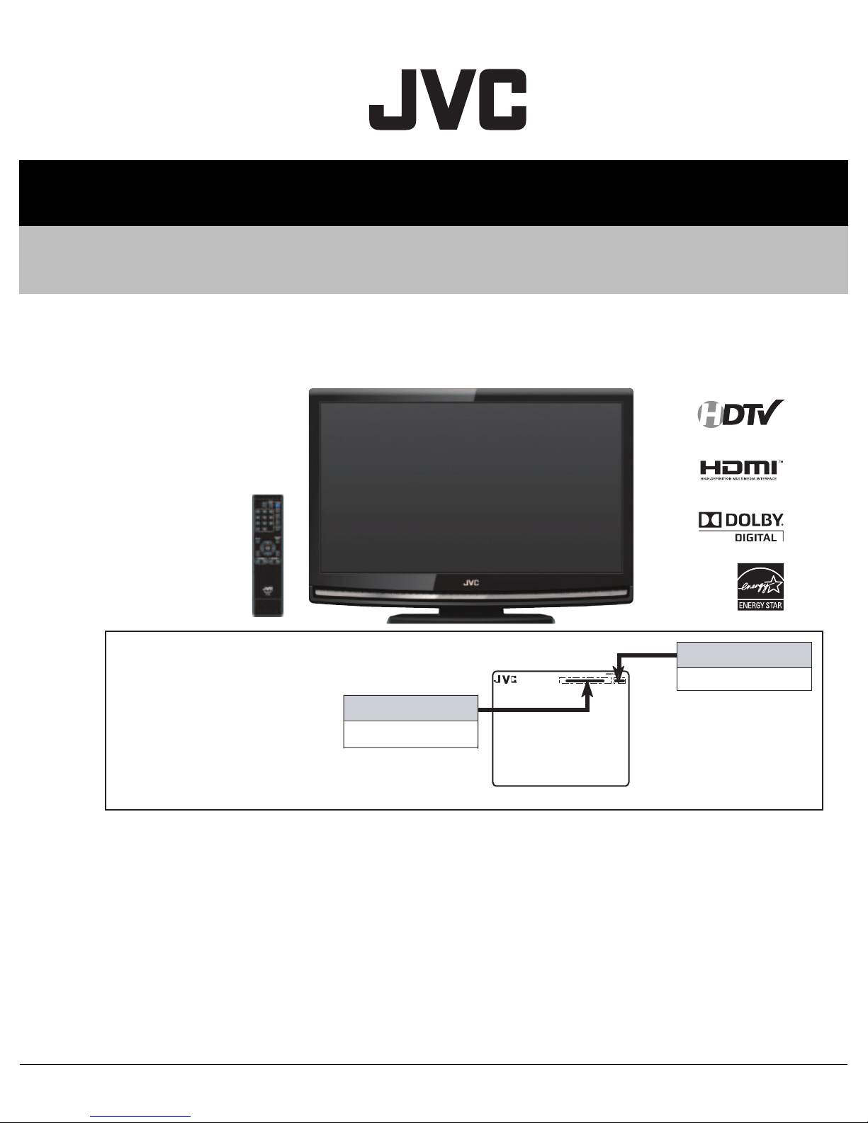
LCD TELEVISION
LT-32A200/AK
HIGH DEFINITION TELEVISION
There may be multiple versions of
this TV model.
The TV version is identified by the
letters next to the model number
on the TV's Rating.
(See illustration).
Use the service manual that
matches the version of the TV.
COPYRIGHT © 2009 Victor Company of Japan, Limited
MODEL NAME
LT-32A200
MODEL NO.
RATING LABEL (REAR)
TABLE OF CONTENTS
1 PRECAUTION. . . . . . . . . . . . . . . . . . . . . . . . . . . . . . . . . . . . . . . . . . . . . . . . . . . . . . . . . . . . . . . . . . . . . . . . . 1-3
2 SPECIFIC SERVICE INSTRUCTIONS . . . . . . . . . . . . . . . . . . . . . . . . . . . . . . . . . . . . . . . . . . . . . . . . . . . . . . 1-4
3 DISASSEMBLY . . . . . . . . . . . . . . . . . . . . . . . . . . . . . . . . . . . . . . . . . . . . . . . . . . . . . . . . . . . . . . . . . . . . . . . 1-8
4 ADJUSTMENT . . . . . . . . . . . . . . . . . . . . . . . . . . . . . . . . . . . . . . . . . . . . . . . . . . . . . . . . . . . . . . . . . . . . . . . 1-12
5 TROUBLESHOOTING . . . . . . . . . . . . . . . . . . . . . . . . . . . . . . . . . . . . . . . . . . . . . . . . . . . . . . . . . . . . . . . . . 1-15
VERSION
AK
COPYRIGHT © 2009 Victor Company of Japan, Limited
No.YA712<Rev.002>
2009/8
Page 2
SPECIFICATION
Items Contents
Dimensions ( W × H × D ) 76.0 cm × 56.3 cm × 23.4 cm (30.0" × 22.2" × 9.3") [with stand]
76.0 cm × 51.93 cm × 11.35 cm (30.0" × 20.5" × 4.5") [without stand]
Mass 9.3 kg (20.6 lbs) [with stand]
Power Input AC120 V , 60 Hz
Power Consumption 155 W (Max)
TV RF System
(Analog / Digital)
Color System (Analog) NTSC
Stereo System (Analog) BTSC (Multi Channel Sound)
Teletext System (Analog) Closed caption (T1-T4 / CC1-CC4)
TV Receiving Channels
and Frequency (Analog)
TV / CATV Total Channel 191 Channels
Intermediate Frequency
(Analog)
Color Sub Carrier Frequency (Analog) 3.58 MHz
LCD Panel 32" class (31.5" Diagonal) wide aspect (16 : 9)
Display Pixels Horizontal : 1366 dots × Vertical : 768 dots (W-XGA)
Audio Power Output 10 W + 10 W
Speaker 1.61" × 2.79", oval type × 2
Antenna Terminal
(VHF/UHF, ATSC / DIGITAL CABLE IN)
Video / Audio Input
[VIDEO]
Video / Audio Input
[COMPONENT]
Digital Input Digital(Video/Audio) HDMI 2-row 19pin connector × 3
Audio output 500mV(rms) (-4dBs), Low impedance, RCA pin jack × 2
Digital Audio output 500 mV (rms), Coaxial × 1
Remote Control Unit RM-C2150 (AA/R6 battery × 2)
Component Video
VHF Low
VHF High
Video IF
Sound IF
S-Video Mini-DIN 4 pin × 1
1080i / 720p
480p / 480i
Analog (Audio) 500mV(rms) (-4dBs), high impedance, RCA pin jack × 2
Design & specifications are subject to change without notice.
8.8 kg (19.5 lbs) [without stand]
Analog
CCIR (M)
Digital
ATSC terrestrial / Digital cable
02 ch - 06 ch : 54 MHz - 88 MHz
07 ch - 13 ch : 174 MHz - 216 MHz
UHF
14 ch - 69 ch : 470 MHz - 806 MHz
CATV
54 MHz - 804 MHz
Low Band : 02 - 06
High Band : 07 - 13
Mid Band : 14 - 22
Super Band : 23 - 36
Hyper Band : 37 - 64
Ultra Band : 65 - 94, 100 - 135
Sub Mid Band : 01, 96 - 99
45.75 MHz
41.25 MHz (4.5 MHz)
F-type connector, 75Ω unbalanced, coaxial × 1
Y: 1 V (p-p), Positive (Negative sync.), 75 Ω
C: 0.286V (p-p) (Burst signal), 75 Ω
Video 1 V (p-p), Positive (Negative sync.), 75 Ω, RCA pin jack × 1
Audio 500 mV (rms), High impedance, RCA pin jack × 2
RCA pin jack × 3
Y : 1 V (p-p) (Sync signal: 0.35V(p-p), 3-value sync.), 75 Ω
Pb/Pr : ±0.35V(p-p), 75 Ω
Y : 1 V (p-p), Positive (Negative sync.), 75 Ω
Cb/Cr : 0.7V(p-p), 75 Ω
Audio 500 mV (rms), High impedance, RCA pin jack × 2
(Digital-input terminal is not compatible with picture signals of personal computer)
Video: Supported format: 1080i / 720p / 480p / 480i
Audio: 2ch L-PCM, 32 / 44.1 / 48 KHz, 16 / 20 / 24 bit
1-2 (No.YA712<Rev.002>)
Page 3
SECTION 1
PRECAUTION
1.1 SAFETY PRECAUTIONS
(1) The design of this product contains special hardware,
many circuits and components specially for safety
purposes. For continued protection, no changes should be
made to the original design unless authorized in writing by
the manufacturer. Replacement parts must be identical to
those used in the original circuits. Service should be
performed by qualified personnel only.
(2) Alterations of the design or circuitry of the products should
not be made. Any design alterations or additions will void
the manufacturer's warranty and will further relieve the
manufacturer of responsibility for personal injury or
property damage resulting therefrom.
(3) Many electrical and mechanical parts in the products have
special safety-related characteristics. These
characteristics are often not evident from visual inspection
nor can the protection afforded by them necessarily be
obtained by using replacement components rated for
higher voltage, wattage, etc. Replacement parts which
have these special safety characteristics are identified in
the parts list of Service manual. Electrical components
having such features are identified by shading on the
schematics and by ( ) on the parts list in Service
manual. The use of a substitute replacement which does
not have the same safety characteristics as the
recommended replacement part shown in the parts list of
Service manual may cause shock, fire, or other hazards.
(4) Don't short between the LIVE side ground and
ISOLATED (NEUTRAL) side ground or EARTH side
ground when repairing.
Some model's power circuit is partly different in the GND.
The difference of the GND is shown by the LIVE : ( ) side
GND, the ISOLATED (NEUTRAL) : ( ) side GND and
EARTH : ( ) side GND.
Don't short between the LIVE side GND and ISOLATED
(NEUTRAL) side GND or EARTH side GND and never
measure the LIVE side GND and ISOLATED (NEUTRAL)
side GND or EARTH side GND at the same time with a
measuring apparatus (oscilloscope etc.). If above note will
not be kept, a fuse or any parts will be broken.
(5) When service is required, observe the original lead dress.
Extra precaution should be given to assure correct lead
dress in the high voltage circuit area. Where a short circuit
has occurred, those components that indicate evidence of
overheating should be replaced. Always use the
manufacturer's replacement components.
(6) Isolation Check (Safety for Electrical Shock Hazard)
After re-assembling the product, always perform an
isolation check on the exposed metal parts of the cabinet
(antenna terminals, video/audio input and output terminals,
Control knobs, metal cabinet, screw heads, earphone jack,
control shafts, etc.) to be sure the product is safe to operate
without danger of electrical shock.
a) Dielectric Strength Test
The isolation between the AC primary circuit and all metal
parts exposed to the user, particularly any exposed metal
part having a return path to the chassis should withstand a
voltage of 3000V AC (r.m.s.) for a period of one second. (.
. . . Withstand a voltage of 1100V AC (r.m.s.) to an
appliance rated up to 120V, and 3000V AC (r.m.s.) to an
appliance rated 200V or more, for a period of one second.)
This method of test requires a test equipment not generally
found in the service trade.
b) Leakage Current Check
Plug the AC line cord directly into the AC outlet (do not use
a line isolation transformer during this check.). Using a
"Leakage Current Tester", measure the leakage current
from each exposed metal part of the cabinet, particularly
any exposed metal part having a return path to the chassis,
to a known good earth ground (water pipe, etc.). Any
leakage current must not exceed 0.5mA AC (r.m.s.).
However, in tropical area, this must not exceed 0.2mA AC
(r.m.s.).
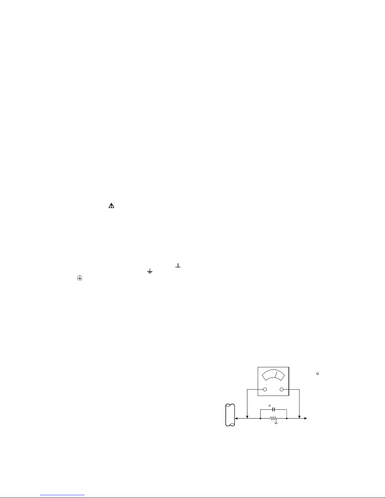
Alternate Check Method
Plug the AC line cord directly into the AC outlet (do not
use a line isolation transformer during this check.). Use
an AC voltmeter having 1000Ω per volt or more
sensitivity in the following manner. Connect a 1500Ω
10W resistor paralleled by a 0.15µF AC-type capacitor
between an exposed metal part and a known good earth
ground (water pipe, etc.). Measure the AC voltage
across the resistor with the AC voltmeter. Move the
resistor connection to each exposed metal part,
particularly any exposed metal part having a return path
to the chassis, and measure the AC voltage across the
resistor. Now, reverse the plug in the AC outlet and
repeat each measurement. Any voltage measured must
not exceed 0.75V AC (r.m.s.). This corresponds to
0.5mA AC (r.m.s.).
However, in tropical area, this must not exceed 0.3V AC
(r.m.s.). This corresponds to 0.2mA AC (r.m.s.).
AC VOLTMETER
(HAVING 1000 /V,
OR MORE SENSITIVITY)
0.15 F AC-TYPE
GOOD EARTH GROUND
1500 10W
PLACE THIS PROBE
ON EACH EXPOSED
ME TAL PAR T
(No.YA712<Rev.002>)1-3
Page 4
SECTION 2
SPECIFIC SERVICE INSTRUCTIONS
2.1 HOW TO IDENTIFY THE TRANS INVERTER
When you replace one of the below Trans Inverters on INVERTER PWB, please replace with the one that has same parts number.
For the part FU-LTZ3PZDAR007, in addition to the lot number,
the letter “DARFON 7609A” is printed on the bottom of the part.
For the part FU-LTZ3PZ0XB009, in addition to the lot number,
the letter ”3PZ0XB009 JS HVT-153” is printed on the bottom of
the part.
Do not mix different parts number’s Trans Inverter.
Part No.: FU-LTZ3PZDAR007
“
DARFON 7609A”
Lot No. Stamp
2.2 STANDARD NOTES FOR SERVICING
2.2.1 CIRCUIT BOARD INDICATIONS
(1) The output pin of the 3 pin Regulator ICs is indicated as
shown.
Part No.: FU-LTZ3PZ0XB009
“
3PZ0XB009 JS HVT-153”
Lot No. Stamp
2.2.2 PB (LEAD) FREE SOLDER
Pb free mark will be found on PCBs which use Pb free
solder. (Refer to figure.) For PCBs with Pb free mark, be sure
to use Pb free solder. For PCBs without Pb free mark, use
standard solder.
Pb free mark
Top View
Bottom View
Input
Out
(2) For other ICs, pin 1 and every fifth pin are indicated as
shown.
In
5
Pin 1
10
(3) The 1st pin of every male connector is indicated as shown.
Pin 1
1-4 (No.YA712<Rev.002>)
Page 5
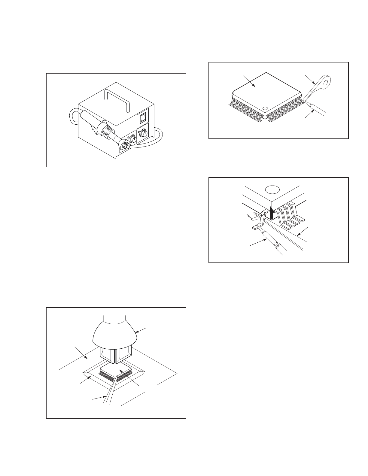
2.2.3 HOW TO REMOVE / INSTALL FLAT PACK-IC
2.2.3.1 REMOVAL
WITH HOT-AIR FLAT PACK-IC DESOLDERING MACHINE:
(1) Prepare the hot-air flat pack-IC desoldering machine,
then apply hot air to the Flat Pack-IC (about 5 to 6
seconds). (Fig.2-1)
Fig.2-1
(2) Remove the flat pack-IC with tweezers while applying
the hot air.
(3) Bottom of the flat pack-IC is fixed with glue to the PWB;
when removing entire flat pack-IC, first apply soldering
iron to center of the flat pack-IC and heat up. Then
remove (glue will be melted). (Fig.2-6)
(4) Release the flat pack-IC from the PWB using tweezers.
(Fig.2-6)
CAUTION:
(1) The Flat Pack-IC shape may differ by models. Use an
appropriate hot-air flat pack-IC desoldering machine,
whose shape matches that of the Flat Pack-IC.
(2) Do not supply hot air to the chip parts around the flat
pack-IC for over 6 seconds because damage to the
chip parts may occur. Put masking tape around the flat
pack-IC to protect other parts from damage. (Fig.2-2)
(3) The flat pack-IC on the PWB is affixed with glue, so be
careful not to break or damage the foil of each pin or
the solder lands under the IC when removing it.
WITH SOLDERING IRON:
(1) Using desoldering braid, remove the solder from all pins
of the flat pack-IC. When you use solder flux which is
applied to all pins of the flat pack-IC, you can remove it
easily. (Fig.2-3)
Flat Pack-IC
Desoldering Braid
Soldering Iron
Fig.2-3
(2) Lift each lead of the flat pack-IC upward one by one,
using a sharp pin or wire to which solder will not adhere
(iron wire). When heating the pins, use a fine tip
soldering iron or a hot air desoldering machine. (Fig.2-4)
Sharp
Pin
Fine Tip
Soldering Iron
Fig.2-4
(3) Bottom of the flat pack-IC is fixed with glue to the PWB;
when removing entire flat pack-IC, first apply soldering
iron to center of the flat pack-IC and heat up. Then
remove (glue will be melted). (Fig.2-6)
(4) Release the flat pack-IC from the PWB using tweezers.
(Fig.2-6)
CBA
Masking
Tape
Tweezers
Fig.2-2
Hot-air
Flat Pack-IC
Desoldering
Machine
Flat Pack-IC
(No.YA712<Rev.002>)1-5
Page 6
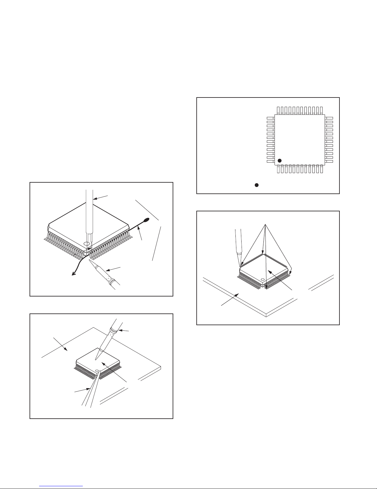
WITH IRON WIRE:
(1) Using desoldering braid, remove the solder from all pins
of the flat pack-IC. When you use solder flux which is
applied to all pins of the flat pack-IC, you can remove it
easily. (Fig.2-3)
(2) Affix the wire to a workbench or solid mounting point, as
shown in Fig.2-5.
(3) While heating the pins using a fine tip soldering iron or
hot air blower, pull up the wire as the solder melts so as
to lift the IC leads from the PWB contact pads as shown
in Fig.2-5.
(4) Bottom of the flat pack-IC is fixed with glue to the PWB;
when removing entire flat pack-IC, first apply soldering
iron to center of the flat pack-IC and heat up. Then
remove (glue will be melted). (Fig.2-6)
(5) Release the flat pack-IC from the PWB using tweezers.
(Fig.2-6)
NOTE:
When using a soldering iron, care must be taken to ensure
that the flat pack-IC is not being held by glue. When the flat
pack-IC is removed from the PWB, handle it gently because
it may be damaged if force is applied.
2.2.3.2 INSTALLATION
(1) Using desoldering braid, remove the solder from the foil of
each pin of the flat pack-IC on the PWB so you can install
a replacement flat pack-IC more easily.
(2) The z mark on the flat pack-IC indicates pin 1. (See Fig.2-
7.) Be sure this mark matches the pin 1 on the PCB when
positioning for installation. Then presolder the four corners
of the flat pack-IC. (See Fig.2-8.)
(3) Solder all pins of the flat pack-IC. Be sure that none of the
pins have solder bridges.
Example :
Pin 1 of the Flat Pack-IC
is indicated by a " " mark.
To Solid
Mounting Point
CBA
Fig.2-5
Hot Air Blower
Iron Wire
Soldering Iron
Fine Tip
Soldering Iron
or
Fig.2-7
Presolder
Flat Pack-IC
CBA
Fig.2-8
Tweezers
Fig.2-6
1-6 (No.YA712<Rev.002>)
Flat Pack-IC
Page 7
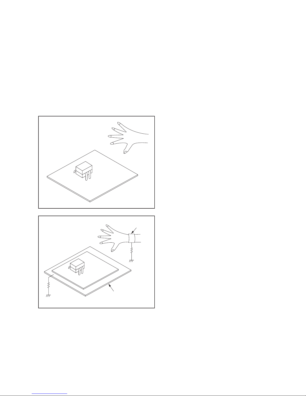
2.2.4 INSTRUCTIONS FOR HANDLING SEMICONDUCTORS
Electrostatic breakdown of the semi-conductors may occur due
to a potential difference caused by electrostatic charge during
unpacking or repair work.
2.2.4.1 Ground for Human Body
Be sure to wear a grounding band (1MΩ) that is properly
grounded to remove any static electricity that may be charged on
the body.
2.2.4.2 Ground for Workbench
Be sure to place a conductive sheet or copper plate with proper
grounding (1MΩ) on the workbench or other surface, where the
semi-conductors are to be placed. Because the static electricity
charge on clothing will not escape through the body grounding
band, be careful to avoid contacting semi-conductors with your
clothing.
<I
ncorrec
t
>
<
C
orrec
1M
CBA
t
>
CBA
Grounding Band
1M
Conductive Sheet or
Copper Plate
(No.YA712<Rev.002>)1-7
Page 8
SECTION 3
DISASSEMBLY
3.1 Disassembly Flowchart
This flowchart indicates the disassembly steps for the cabinet
parts, and the CBA in order to gain access to item(s) to be serviced. When reassembling, follow the steps in reverse order.
Bend, route and dress the cables as they were.
[1] Stand
Assembly
[10] Junction
CBA
3.2 Disassembly Method
[2] Rear Cabinet
[3] Inverter CBA
[4] Jack CBA
[5] Power Supply
CBA
[6] Jack Holder
[7] Digital Main
CBA Unit
[13] LCD Module
Assembly
[14] Front
Cabinet
[8] Speaker
Holder (L,R)
[9] Speaker(s)
[11] IR Sensor
CBA
[12] Function
CBA
Removal
Step/
Loc.
No.
Part
Remove/*Unhook/
Fig.
No.
Unlock/Release/
Unplug/Unclamp/
Note
Desolder
Stand
[1]
[2]
Assembly
Rear
Cabinet
D1 4(S-1) ---
D1 13(S-2), 2(S-3), 3(S-4) ---
6(S-5), *CN1001,
[3]
Inverter
CBA
D2
*CN1003, *CN1050,
D4
*CN1100, *CN1150,
---
*CN1200, *CN1900
Removal
Step/
Loc.
No.
Part
Remove/*Unhook/
Fig.
No.
Unlock/Release/
Unplug/Unclamp/
Desolder
Digital Main
[7]
CBA UnitD2D4
4(S-9), 2(S-10),
4(S-11), *CN3902,
Shield Box
Speaker
[8]
Holder
D3 *Hook ---
(L,R)
[9] Speaker(s) D3 8(S-12) ---
[10]
[11]
[12]
Junction
CBA
IR Sensor
CBA
Function
CBA
D3
Desolder ---
D4
D3
2(S-13), *CL103C ---
D4
D3
2(S-14) ---
D4
LCD
[13]
Module
D3 (S-15) ---
Assembly
Front
[14]
Cabinet
D3 --------------- ---
(1) (2) (3) (4) (5)
NOTE;
(1) Order of steps in procedure. When reassembling, follow
the steps in reverse order. These numbers are also used
as the Identification (location) No. of parts in figures.
(2) Parts to be removed or installed.
(3) Fig. No. showing procedure of part location
(4) Identification of parts to be removed, unhooked, un-
locked, released, unplugged, unclamped, or desoldered.
P = Spring, L = Locking Tab, S = Screw, H = Hex Screw,
CN = Connector * = Unhook, Unlock, Release, Unplug,
or Desolder e.g. 2(S-2) = two Screws (S-2), 2(L-2) = two
Locking Tabs (L-2)
(5) Refer to the following "Reference Notes in the Table."
Note
---
[4] Jack CBA
Power
[5]
Supply
CBA
D2
2(S-6), *CL701B ---
D4
7(S-7), *CN101,
D2
*CN301, *CN302,
D4
*CN801, *CN802
[6] Jack Holder D2 2(S-8) ---
1-8 (No.YA712<Rev.002>)
---
Page 9

(S-4)
(S-2)
[2] Rear Cabinet
[1] Stand Assembly
(S-2)
(S-1)
(S-3)
(S-4)
(S-2)
(S-4)
(S-2)
Fig. D1
(No.YA712<Rev.002>)1-9
Page 10

[3] Inverter CBA
(S-5)
(S-11)
[7] Digital Main
CBA Unit
(S-8)
[4] Jack CBA
Shield Box
[6] Jack Holder
(S-6)
(S-9)
(S-10)
(S-9)
(S-7)
(S-7)
(S-7)
(S-5)
[5] Power Supply CBA
Fig. D2
1-10 (No.YA712<Rev.002>)
Page 11

[14] Front Cabinet
[13] LCD Module
Assembly
Hook
[10] Junction
CBA
(S-12)
[9] Speaker
[8] Speaker Holder (L)
(S-15)
Hook
[8] Speaker Holder (R)
[11] IR Sensor CBA
(S-13)
(S-12)
[9] Speaker
[12] Function CBA
(S-14)
Fig. D3
(No.YA712<Rev.002>)1-11
Page 12

SECTION 4
ADJUSTMENT
4.1 GENERAL NOTE: "PWB" IS ABBREVIATION FOR
"CIRCUIT BOARD ASSEMBLY."
NOTE:
Electrical adjustments are required after replacing circuit components and certain mechanical parts. It is important to perform these adjustments only after all repairs and replacements
have been completed. Also, do not attempt these adjustments
unless the proper equipment is available.
4.2 TEST EQUIPMENT REQUIRED
(1) NTSC Pattern Generator (Color Bar W/White Window, Red
Color, Dot Pattern, Gray Scale, Monoscope, Multi-Burst)
(2) Remote control unit
(3) Color Analyzer
4.3 HOW TO MAKE THE SERVICE REMOTE CONTROL
UNIT:
Cut "A" portion of the attached remote control unit as shown in
Fig. 1.
service button
(There is a button under the plastic housing.)
4.5 PURITY CHECK MODE
This mode cycles through full-screen displays of red, green, blue,
and white to check for non-active pixels.
(1) Enter the Service mode.
(2) Each time pressing [7] button on the service remote control
unit, the display changes as follows.
Purity Check Mode
White mode
[7] button
[7] button
Black mode
[7] button
Red mode
A
4.4 HOW TO SET UP THE SERVICE MODE:
Service mode:
(1) Use the service remote control unit.
(2) Turn the power on.
(3) Press the service button on the service remote control
unit. The following screen appears.
"*" differs depending on the models.
Code :
***********-***
Pic code :
**-***-**-*****-***
MIPS :
Push 0key
Tuner :
****-*****-****
safety_Non
Safety :
[7] button
Green mode
Fig. 1
[7] button
Blue mode
[7] button
White 20% mode
Note:
When entering this mode, the default setting is White mode.
1-12 (No.YA712<Rev.002>)
Page 13

4.6 VCOM ADJUSTMENT
Test Point Adj. Point
Screen
M. EQ. Spec.
Color analyzer See below
To avoid interference from ambinent
light, this adjustment should be
performed in a dark room.
Perpendicularity
L = 3 cm
[CHANNEL UP/DOWN ]
buttons
Figure
Color Analyzer
4.7 WHITE BALANCE ADJUSTMENT
The white balance adjustment should be performed when
replacing the LCD Panel or Digital PWB.
Purpose: To mix red, green and blue beams correctly for pure
white.
Symptom of Misadjustment: White becomes bluish or reddish.
Test Point
Screen
Adj. Point Mode Input
[VOLUME
DOWN]
button
[VIDEO1]
C/D
White Raster
(APL 70%)
or
(APL 40%)
M. EQ. Spec.
Pattern Generator,
Color analyzer
x= 0.272 ± 0.005
y= 0.278 ± 0.005
Figure
To avoid interference from ambinent
light, this adjustment should be
performed in a dark room.
Perpendicularity
(1) Operate the unit for more than 20 minutes.
(2) Set the color analyzer and bring the optical receptor to the
center on the LCD-Panel surface after zero point calibration as shown above. Note: The optical receptor must be
set perpendicularly to the LCD Panel surface.
(3) Enter the Service mode.
(4) Press [3] button on the service remote control unit.
(5) Press [CHANNEL UP/DOWN] buttons on the service re-
mote control unit so that the color analyzer value becomes
minimum.
L = 3 cm
INPUT: WHITE 70%, 40%
(1) Operate the unit for more than 20 minutes.
(2) Input the White Raster(70%=70IRE, 40%=40IRE).
INPUT SIGNAL
0IRE 0IRE
100IRE
40%=40IRE
(3) Set the color analyzer to the CHROMA mode and bring the
optical receptor to the center on the LCD-Panel surface after zero point calibration as shown above.
Note: The optical receptor must be set perpendicularly to
the LCD Panel surface.
(4) Enter the Service mode. Press [VOLUME DOWN] button
on the service remote control unit and select "C/D" mode.
(5) [CUTOFF]
Press [1] button to select “COR” for Red Cutoff adjustment.
Press [3] button to select “COB” for Blue Cutoff adjustment.
[DRIVE]
Press [4] button to select “DR” for Red Drive adjustment.
Press [6] button to select “DB” for Blue Drive adjustment.
(6) In each color mode, press [CHANNEL UP/DOWN] buttons
to adjust the values of color.
(7) Adjust Cutoff and Drive so that the color temperature be-
comes 12000°K (x= 0.272 / y= 0.278 ±0.005).
Color Analyzer
Low
Hight
Light
Light
70%=70IRE
100IRE
(No.YA712<Rev.002>)1-13
Page 14

4.8 HOW TO INITIALIZE THE LCD TV/DVD
The purpose of initialization is to place the set in a new out of box
condition. The customer will be prompted to
select a language and program channels after the set has been
initialized.
To put the program back at the factory-default, initialize the LCD
TV using the following procedure.
(1) Turn the power on.
(2) To enter the service mode, press the service button on the
service remote control unit.
- To cancel the service mode, press [POWER] button on
the service remote control unit.
(3) Press [INFO] button on the service remote control unit to
initialize the LCD television.
(4) "INITIALIZED" will appear in the upper right of the screen.
"INITIALIZED" color will change to green from red when initializing is complete.
4.9 FIRMWARE RENEWAL MODE
4.9.1 EQUIPMENT REQUIRED
a. USB memory
b. Remote Control Unit
4.9.2 FIRMWARE UPDATE PROCEDURE
NOTE:
There are two states (the User Upgrade and the Factory Upgrade) in firmware update.
Software Upgrade
Software upgrade in progress. Please wait.
Do not remove the USB device or turn the TV off
while upgrade is in progress.
*1
Downloading...
0%
NOTE:
If the above screen isn’t displayed, repeat from step 1.
The appearance shown in *1 is described as follows.
Appearance State
Downloading... Downloading the firmware from the USB
memory.
Writing... Writing the downloaded firmware in flash
memory.
Checking... Checking the new firmware.
(5) When the firmware update is completed, the following will
appear on the screen.
Software Upgrade
User Upgrade Upgrade the firmware only. The
setting values are not initialized.
Factory upgrade Upgrade the firmware and initialize
the setting values.
The identification of User Upgrade and Factory Upgrade are
done by the filename.
(1) Turn the power off and unplug the AC Cord.
(2) Insert the USB memory to the USB port as shown below.
Rear Cabinet
USB Memory
The software upgrade is completed.
Remove USB storage device, unplug and replug power code.
Unplug the AC cord and kindly remove the USB memory
from the USB port. Plug the AC cord in the wall outlet again
and turn the power on.
NOTE:
When the Factory Upgrade is used, after restarting TV,
shift to initial screen menu in service mode. "INITIALIZED" will appear on the upper right of the screen. "INITIALIZED" color will change to green from red when
initializing is complete.
(3) Plug the AC cord in the wall outlet and turn the power on.
(4) The update will start and the following will appear on the
screen.
1-14 (No.YA712<Rev.002>)
Page 15

5.1 Power Supply Section
FLOW CHART NO.1
The power cannot be turned on.
SECTION 5
TROUBLESHOOTING
Is the fuse (F601) normal?
Ye s
Is normal state restored when once un
power cord is plugged again several seconds?
Ye s
Is the AL+33V line voltage normal?
Ye s
Check each rectifying circuit of the secondar
circuit and service it if def
FLOW CHART NO.2
The fuse blows out.
Check the prese
is leaking or shorted and ser
After servicing, replace the fuse.
FLOW CHART NO.3
When the output voltage fluctuates.
nce that the pr
ective.
imary component
vice it if de
plugged
fective.
No
No
No
y
See FLOW CHART No.2 <The fuse blows out.>
Check if there is any leak or short-circuiting on the
primary circuit component, and service it if defective.
(C605, D601, D602, D603, D604, Q601, Q602,
T601)
Check the presence that the rectifying diode or circuit
is shorted in each rectifying circuit of secondar
and service it if defective.
y side,
Does the photocoupler circuit on
secondary side operate normally?
Check IC601, D609, D611 and their per
circuit and service it if def
FLOW CHART NO.4
When buzz sound can be heard in the vicinity of power circuit.
Check if there is any short-circuit on the rectifying diode and the circuit
and service it if defective. (IC631, Q207, Q209, Q210, Q211, Q501, Q635, Q636, Q637, Q640, Q641, Q64
D631, D632, D633, D638, D641, D642, D646, D
FLOW CHART NO.5
AL+33V is not output.
Is approximately +34V voltage supplied to the
cathode of D638?
Check D657, R661 and their peripher
service it if defective.
the
Ye s
iphery,
ective.
647)
Ye s
y circuit, and
No
No
Check IC601, D652, Q631 and their periphery
circuit, and service it if defective.
in each rectifying circuit of the secondary side
Check C638, D638, D639 and their periphery
circuit, and service it if defective.
,
2, Q643,
(No.YA712<Rev.002>)1-15
Page 16

FLOW CHART NO.6
LCD+24.5V is not output.
Is approximately +30V voltage supplied to the collector
of Q210?
Ye s
Check Q207, Q208, D205, P-ON-H1 line and their
periphery circuit, and service it if defective.
FLOW CHART NO.7
LCD+16V is not output.
Is approximately +19V voltage supplied to the
collector of Q209?
Ye s
Is approximately +16V voltage supplied to the
base of Q209?
Ye s
Replace Q209.
FLOW CHART NO.8
INV+16V is not output.
No
No
No
See FLOW CHART No.5
Check C631, D631, D635 and their per
iphery circuit,
and service it if defective.
Check Q207, Q208, D203, D204, D211 and their
periphery circuit, and service it if defective.
Is approximately +19V voltage supplied to the
collector of Q501?
Ye s
Is approximately +16V voltage supplied to the
base of Q501?
Ye s
Replace Q501.
FLOW CHART NO.9
P-ON+7V is not output.
Is approximately +7V voltage supplied to the
collector of D646?
Ye s
Check if there is any leak or shor
t-circuit on
the loaded circuit, and service it if defective.
No
No
No
Check C631, D631, D635 and their periphery circuit,
and service it if defective.
Check Q207, Q208, D203, D204, D211 and their
periphery circuit, and service it if defective.
Check C644, D646 and their periphery circuit,
and service it if defective.
1-16 (No.YA712<Rev.002>)
Page 17

FLOW CHART NO.10
P-ON+5V is not output. (LCD+16V is outputted normally.)
Is approximately +6.8V voltage supplied to the
No
collector of Q643?
Ye s
Is approximately +6V voltage supplied to the
No
base of Q641 and the base of Q643?
Ye s
Replace Q641 and Q643.
FLOW CHART NO.11
P-ON+5V(TUNER+5V) is not output. (LCD+16V is outputted normally.)
Is approximately +6.7V voltage supplied to the
No
collector of Q640?
Ye s
Is approximately +6V voltage supplied to the
No
base of Q641 and the base of Q643(Q640)?
Ye s
Replace Q641 and Q643(Q640).
See FLOW CHART No.9
Check D645 and their periphery circuit, and service
it if defective.
See FLOW CHART No.9
Check D645 and their periphery circuit, and service
it if defective.
FLOW CHART NO.12
AL+13V(M+13V) is not output.
Is approximately +13V voltage supplied to the
cathode of D641 and D642?
Ye s
Check if there is any leak or short-circuit on
the loaded circuit, and service it if def
ective.
FLOW CHART NO.13
P-ON+3V is not output.
Is approximately +3V voltage supplied to the
cathode of D647?
Ye s
Check if there is any leak or shor
the loaded circuit, and service it if def
t-circuit on
ective.
No
No
Check C639, D642 and their periphery circuit, and
service it if defective.
Check C645, D647 and their per
service it if def
ective.
iphery circuit, and
(No.YA712<Rev.002>)1-17
Page 18

FLOW CHART NO.14
P-ON+3.3V is not output.
Is approximately +5V voltage supplied to the
cathode of D633?
Ye s
Is the "H" signal (approximately +3.5V) inputted to the
base of Q637?
Ye s
Replace Q637.
FLOW CHART NO.15
P-ON+9V is not output. (LCD+16V is outputted normally.)
Is approximately +13V voltage supplied to t
he
collector of Q642?
Ye s
Is approximately +10V voltage supplied to the
base of Q642?
Ye s
Replace Q642.
No
No
No
No
Check C633, D633 and their periphery circuit, and
service it if defective.
Check Q638, Q639, P-ON-H2 line and their periphery
circuit, and service it if def
ective.
See FLOW CHART No.12
Check D670 and their periphery circuit, and service
it if defective.
FLOW CHART NO.16
AL+3.3V is not output.
Is approximately +34V voltage supplied to the
collector of Q635?
Ye s
Is approximately +5V voltage supplied to Pin(1) of
IC631?
Ye s
Replace IC631.
FLOW CHART NO.17
LCD-6.8V is not output.
Is approximately -9V voltage supplied to the
Anode of D632?
Ye s
Is approximately -8V voltage supplied to the
base of Q211?
Ye s
No
No
No
No
See FLOW CHART No.5
Check Q635, D659 and their per
iphery circuit, and
service it if defective.
Check C632, D632 and their periphery
circuit, and service it if defective.
Check Q207, Q208, D205, P-ON-H1 line and their
periphery circuit, and service it if defective.
Replace Q211.
1-18 (No.YA712<Rev.002>)
Page 19

5.2 Video Signal Section
FLOW CHART NO.1
The key operation is not functioning.
Are the contact point and installation state of the k
switches (SW101A, SW103A~SW107A) nor
mal?
Ye s
When pressing each switches (SW101A, SW103A~
SW107A) do the voltage of Pin(29) of CN302 and
Pin(2) of CN303 increase?
Ye s
Replace Digital Main PWB Unit.
FLOW CHART NO.2
No operation is possible from the remote control unit.
Operation is possible from the remote control unit.
Is 3.3V voltage supplied to Pin(2) terminal of the
remote control receiver (RS102)?
Ye s
Is the "L" pulse sent out Pin(1) terminal of remote
control receiver (RS102) when the infrared remote
control is activated?
Ye s
Is the "L" pulse supplied to Pin(25) of CN301?
Ye s
Replace Digital Main PWB Unit.
ey
No
No
No
No
No
Re-install the switches (SW101A, SW103A~SW107A)
correctly or replace the poor switch.
Check the switches (SW101A, SW103A~SW107A)
and their periphery, and service it if defective.
Check AL+3.3V line and service it if defective.
Replace the remote control receiver(RS102)
or the remote control unit.
Check the line between Pin(1) terminal of remote
control receiver(RS102) and Pin(25) of CN301,
and service it if defective.
FLOW CHART NO.3
Picture does not appear normally.(Video input)
Are the video signal inputted to Pin
Ye s
Replace Digital Main PWB Unit or LCD Module
Assembly.
(4) of CN302?
No
Check the line between Pin(4) of CN302 and
JK752, and service it if defective.
(No.YA712<Rev.002>)1-19
Page 20

FLOW CHART NO.4
Picture does not appear normally.(Tuner input)
Are the DIF signal inputted to the Pin(26,28) of CN302?
Ye s
Replace Digital Main PWB Unit or LCD Module
Assembly.
FLOW CHART NO.5
Picture does not appear normally.(S-Video input)
Are the video signal o
utputted to the Pin(6, 8) of
CN302?
Pin(6): S-VIDEO-C
Pin(8): S-VIDEO-Y
Ye s
Replace Digital Main PWB Unit
or LCD Module
Assembly.
FLOW CHART NO.6
Picture does not appear normally.(Y/Pb/Pr input)
No
No
Check the line between Pin(26, 28) of CN302 and
Pin(10, 11) of TU301, and service it if defective.
Check the line between Pin(6, 8) of CN302 and
JK751, and service it if defective.
Are the video signal inputted to the Pin(15, 17, 19) of
CN302?
Pin(15): VIDEO-Y
Pin(17): VIDEO-Pb
Pin(19): VIDEO-Pr
Ye s
Replace Digital Main
PWB Unit or LCD Module
Assembly.
No
Check the line between Pin(15, 17, 19) of CN302
and input terminals(JK731, JK732, JK733), and
service it if defective.
1-20 (No.YA712<Rev.002>)
Page 21

5.3 Audio Signal Section
FLOW CHART NO.1
Audio is not outputted normally.(Audio input)
Are the audio(L/R) signals inputted to Pin(2, 15)
of IC771?
Ye s
Are the audio(L/R) si
gnals inputted to each pin of
CN301?
Pin(6) :
Pin(8) :
Pin(2) :
Pin(4) :
AMP(L)-OUT
AMP(R)-OUT
AUDIO(L)-OUT
AUDIO(R)-OUT
Ye s
Are the audio(L/R) signals inputted to the Pin
(1, 44)
of IC801?
Are the audio(L/R) si
gnals inputted to the Pin(3, 5)
of IC871?
Ye s
Are the audio(L/R) signals outputte
d to the Pin(1, 2)
of CN801 and CN802?
CN802: SP(L)
CN801: SP(R)
Are the audio(L/R) signals outputte
output ter
minal?
d to the audio
JK871: AUDIO(L)-OUT
JK872: AUDIO(R)-OUT
No
No
No
No
No
Ye s
No
Check the line between Pin(2, 15) of IC771 and
input terminal(JK753, JK754), and service it if
defective.
Replace Digital Main
PWB Unit.
Check the line between Pin(6, 8) of CN301 and
Pin(1, 44) of IC801, and
Check the line betw
service it if de
een Pin(2, 4) of CN301 and
Pin(3, 5) of IC871, and service it if de
fective.
fective.
Check IC801 and their periphery circuit, and
service it if def
ective.
Check SP801,SP802 and their periphery circuit,
and service it if defective.
Check the line betw
een Pin(1,
7) of IC871 and audio
output terminal(JK871, JK872), and service it if
defective.
(No.YA712<Rev.002>)1-21
Page 22

FLOW CHART NO.2
Audio is not outputted normally.(Component Audio input)
Are the audio(L/R) signals inputted to the Pin(4, 11)
of IC771?
Ye s
Are the audio(L/R) signals inputted to each pin of
CN301?
Pin(6) :
Pin(8) :
Pin(2) :
Pin(4) :
AMP(L)-OUT
AMP(R)-OUT
AUDIO(L)-OUT
AUDIO(R)-OUT
Ye s
Are the audio(L/R) signals inputted to the Pin
(1, 44)
of IC801?
Are the audio(L/R) signals inputted to the Pin(3, 5)
of IC871?
Ye s
Are the audio(L/R) signals outputte
d to the Pin(1, 2)
of CN801 and CN802?
CN802: SP(L)
CN801: SP(R)
Are the audio(L/R) signals outputte
d to the audio
output terminal?
JK871: AUDIO(L)-OUT
JK872: AUDIO(R)-OUT
No
No
No
No
No
Ye s
No
Check the line between Pin(4, 11) of IC771 and
input terminal(JK741, JK742), and service it if
defective.
Replace Digital Main PWB Unit.
Check the line between Pin(6, 8) of CN301 and
Pin(1, 44) of IC801, and service it if def
Check the line between Pin(2, 4) of CN301
Pin(3, 5) of IC871, and ser
vice it if de
ective.
f
ective.
and
Check IC801 and their periphery circuit, and
service it if def
ective.
Check SP801,SP802 and their periphery circuit,
and service it if defective.
Check the line between Pin(1, 7) of IC871 and audio
output terminal(JK871, JK872), and service it if
defective.
1-22 (No.YA712<Rev.002>)
Page 23

FLOW CHART NO.3
Audio is not outputted normally.(Tuner input)
Are the DIF signals outputted to the Pin(26, 28)
of CN302?
Ye s
Are the audio(L/R) signals inputted to each pin of
CN301?
Pin(6) :
Pin(8) :
Pin(2) :
Pin(4) :
AMP(L)-OUT
AMP(R)-OUT
AUDIO(L)-OUT
AUDIO(R)-OUT
Ye s
Are the audio(L/R) signals inputted to the Pin(1, 44)
of IC801?
Are the audio(L/R) signals inputted to the Pin(3, 5)
of IC871?
Ye s
Are the audio(L/R) signals outputted to the Pin(1, 2)
of CN801 and CN80
2?
CN802: SP(L)
CN801: SP(R)
Are the audio(L/R) signals outputte
d to the audio
output terminal?
JK871: AUDIO(L)-OUT
JK872: AUDIO(R)-OUT
No
No
No
No
No
Ye s
No
Check TU301 and their periphery circuit, and
service it if defective.
Replace Digital Main PWB Unit.
Check the line between Pin(6, 8) of CN301 and
Pin(1, 44) of IC801, and
service it if de
fective.
Check the line between Pin(2, 4) of CN301 and
Pin(3, 5) of IC871, and service it if de
fective.
Check IC801 and their periphery circuit, and
service it if def
ective.
Check SP801,SP802 and their periphery circuit,
and service it if defective.
Check the line between Pin(1, 7) of IC871 and audio
output terminal(JK871, JK872), and service it if
defective.
(No.YA712<Rev.002>)1-23
Page 24

Victor Company of Japan, Limited
Display Division 12, 3-chome, Moriya-cho, Kanagawa-ku, Yokohama-city, Kanagawa-prefecture, 221-8528, Japan
(No.YA712<Rev.002>)
Printed in Japan
VSE
 Loading...