

Page 1
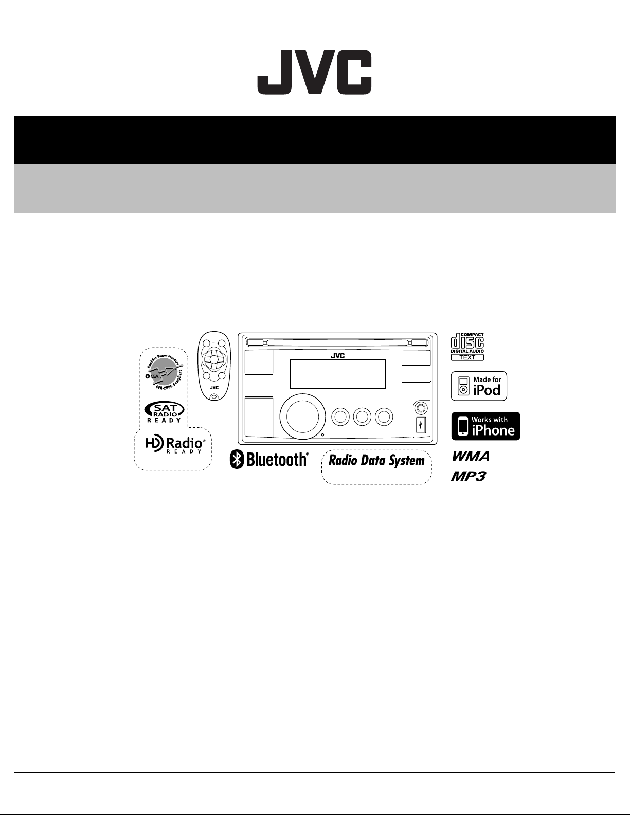
SERVICE MANUAL
CD RECEIVER
MA475<Rev.001>20103SERVICE MANUAL
KW-XR810J, KW-XR816U, KW-XR816UH,
KW-XR811E, KW-XR811EY, KW-XR811EU,
KW-XR817EE
except
KW-XR817
only KW-XR810
For KW-XR811/XR817
COPYRIGHT © 2010 Victor Company of Japan, Limited
Lead free solder used in the board (material : Sn-Ag-Cu, melting point : 219 Centigrade)
Lead free solder used in the board (material : Sn-Cu, melting point : 230 Centigrade)
TABLE OF CONTENTS
1 PRECAUTION. . . . . . . . . . . . . . . . . . . . . . . . . . . . . . . . . . . . . . . . . . . . . . . . . . . . . . . . . . . . . . . . . . . . . . . . . 1-5
2 SPECIFIC SERVICE INSTRUCTIONS . . . . . . . . . . . . . . . . . . . . . . . . . . . . . . . . . . . . . . . . . . . . . . . . . . . . . . 1-9
3 DISASSEMBLY . . . . . . . . . . . . . . . . . . . . . . . . . . . . . . . . . . . . . . . . . . . . . . . . . . . . . . . . . . . . . . . . . . . . . . . 1-9
4 ADJUSTMENT . . . . . . . . . . . . . . . . . . . . . . . . . . . . . . . . . . . . . . . . . . . . . . . . . . . . . . . . . . . . . . . . . . . . . . . 1-21
5 TROUBLESHOOTING . . . . . . . . . . . . . . . . . . . . . . . . . . . . . . . . . . . . . . . . . . . . . . . . . . . . . . . . . . . . . . . . . 1-24
COPYRIGHT © 2010 Victor Company of Japan, Limited
No.MA475<Rev.001>
2010/3
Page 2
SPECIFICATION
KW-XR810
AUDIO AMPLIFIER SECTION
Power Output 20 W RMS × 4 Channels at 4 Ω and < 1% THD+N
Signal-to-Noise Ratio 80 dBA (reference: 1 W into 4 Ω)
Load Impedance 4 Ω (4Ω to 8 Ω allowance)
Tone Control Range Bass ±12 dB (50 Hz, 100 Hz, 200 Hz) Q0.7, Q1.0, Q1.4, Q2.0
Middle ±12 dB (0.5 kHz, 1.0 kHz, 2.0 kHz) Q0.7, Q1.0, Q1.4, Q2.0
Treble ±12 dB (5.0 kHz, 10.0 kHz, 15.0 kHz) Q0.7, Q1.0, Q1.4, Q2.0
Frequency Response 40 Hz to 20 000 Hz
Line-Out Level/Impedance 2.5 V/20 kΩ load (full scale)
Subwoofer-Out Level/Impedance 2.5 V/20 kΩ load (full scale)
Output Impedance 1 kΩ
Other Terminal AUX (auxiliary) input jack, USB input terminal, USB cable, Antenna input, Expansion
port, Steering wheel remote input
TUNER SECTION
Frequency Range FM with channel interval set to 100 kHz or 200 kHz
with channel interval set to 50 kHz
AM with channel interval set to 10 kHz
with channel interval set to 9 kHz
FM Tuner Usable Sensitivity 9.3 dBf (0.8 µV/75 Ω)
50 dB Quieting Sensitivity 16.3 dBf (1.8 µV/75 Ω)
Alternate Channel Selectivity (400 kHz) 65 dB
Frequency Response 40 Hz to 15 000 Hz
Stereo Separation 40 dB
AM Tuner Sensitivity 20 µV
Selectivity 40 dB
CD PLAYER SECTION
Type Compact disc player
Signal Detection System Non-contact optical pickup (semiconductor laser)
Number of Channels 2 channels (stereo)
Frequency Response 5 Hz to 20 000 Hz
Dynamic Range 96 dB
Signal-to-Noise Ratio 98 dB
Wow and Flutter Less than measurable limit
MP3 Decoding Format: (MPEG1/2 Audio Layer 3) Max. Bit Rate: 320 kbps
WMA (Windows Media
USB SECTION
USB Standard USB 1.1, USB 2.0
Data Transfer Rate Full Speed Max. 12 Mbps
Compatible Device Mass storage class (except HDD)
Compatible File System FAT 32/16/12
Playable Audio Format MP3/WMA/WAV
Max. Current DC 5 V 500 mA
BLUETOOTH
Version Bluetooth 2.0 certified
Power Class Class 2 Radio (possible distance 10 m)
Service Area 10 m
Profile HFP 1.5, OPP 1.1, A2DP 1.2, AVRCP 1.3, PBAP 1.0
Max. Current DC 5 V 54.3 mA
GENERAL
Power Requirement Operating Voltage DC 14.4 V (11 V to 16 V allowance)
Grounding System Negative ground
Allowable Operating Temperature 0°C to +40°C (32°F to 104°F)
Dimensions (W × H × D)
(approx.)
Mass 1.9 kg (4.2 lbs) (excluding accessories)
Designs & specifications are subject to change without notice.
® Audio) Decoding Format Max. Bit Rate: 320 kbps
Low Speed Max. 1.5 Mbps
Installation Size 182 mm × 111 mm × 160 mm (7-3/16” × 4-3/8” × 6-5/16”)
Panel Size 188 mm × 117 mm × 23 mm (7-7/16” × 4-5/8” × 5/16”)
1-2 (No.MA475<Rev.001>)
Page 3
KW-XR811, KW-XR817
AUDIO AMPLIFIER SECTION
Maximum Power Output Front/Rear 50 W per channel
Continuous Power Output (RMS)
Load Impedance 4 Ω (4Ω to 8 Ω allowance)
Tone Control Range Bass ±12 dB (50 Hz, 100 Hz, 200 Hz) Q0.7, Q1.0, Q1.4, Q2.0
Frequency Response 40 Hz to 20 000 Hz
Signal-to-Noise Ratio 70 dB
Line-Out Level/Impedance 2.5 V/20 kΩ load (full scale)
Subwoofer-Out Level/Impedance 2.5 V/20 kΩ load (full scale)
Output Impedance 1 kΩ
Other Terminal AUX (auxiliary) input jack, USB input terminal, USB cable, Aerial input, Steering wheel
TUNER SECTION
Frequency Range FM 87.5 MHz to 108.0 MHz
FM Tuner Usable Sensitivity 9.3 dBf (0.8 µV/75 Ω)
MW Tuner Sensitivity 20 µV
AM Tuner Selectivity 40 dB
CD PLAYER SECTION
Type Compact disc player
Signal Detection System Non-contact optical pickup (semiconductor laser)
Number of Channels 2 channels (stereo)
Frequency Response 5 Hz to 20 000 Hz
Dynamic Range 96 dB
Signal-to-Noise Ratio 98 dB
Wow and Flutter Less than measurable limit
MP3 Decoding Format: (MPEG1/2 Audio Layer 3) Max. Bit Rate: 320 kbps
WMA (Windows Media
USB SECTION
USB Standard USB 1.1, USB 2.0
Data Transfer Rate Full Speed Max. 12 Mbps
Compatible Device Mass storage class (except HDD)
Compatible File System FAT 32/16/12
Playable Audio Format MP3/WMA/WAV
Max. Current DC 5 V 500 mA
BLUETOOTH
Version Bluetooth 2.0 certified
Power Class Class 2 Radio (possible distance 10 m)
Service Area 10 m
Profile HFP 1.5, OPP 1.1, A2DP 1.2, AVRCP 1.3, PBAP 1.0
Max. Current DC 5 V 54.3 mA
GENERAL
Power Requirement Operating Voltage DC 14.4 V (11 V to 16 V allowance)
Grounding System Negative ground
Allowable Operating Temperature 0°C to +40°C
Dimensions (W × H × D):
(approx.)
Mass 1.9 kg (excluding accessories)
Designs & specifications are subject to change without notice.
Front/Rear 20 W per channel into 4 Ω, 40 Hz to 20 000 Hz at no more than 1% total harmonic
distortion.
Middle ±12 dB (0.5 kHz, 1.0 kHz, 2.0 kHz) Q0.7, Q1.0, Q1.4, Q2.0
Treble ±12 dB (5.0 kHz, 10.0 kHz, 15.0 kHz) Q0.7, Q1.0, Q1.4, Q2.0
remote input(KW-XR811)
FM-LOW (KW-XR817) 65.0 MHz to 74.0 MHz
AM MW: 522 kHz to 1 620 kHz
LW: 144 kHz to 279 kHz
50 dB Quieting Sensitivity 16.3 dBf (1.8 µV/75 Ω)
Alternate Channel Selectivity (400 kHz) 65 dB
Frequency Response 40 Hz to 15 000 Hz
Stereo Separation 40 dB
Sensitivity 50 µV
® Audio) Decoding Format Max. Bit Rate: 320 kbps
Low Speed Max. 1.5 Mbps
Installation Size 182 mm × 111 mm × 160 mm
Panel Size 188 mm × 117 mm × 23 mm
(No.MA475<Rev.001>)1-3
Page 4
KW-XR816
AUDIO AMPLIFIER SECTION
Maximum Power Output Front/Rear 50 W per channel
Continuous Power Output (RMS)
Load Impedance 4 Ω (4Ω to 8 Ω allowance)
Tone Control Range Bass ±12 dB (50 Hz, 100 Hz, 200 Hz) Q0.7, Q1.0, Q1.4, Q2.0
Frequency Response 40 Hz to 20 000 Hz
Signal-to-Noise Ratio 70 dB
Line-Out Level/Impedance 5.0 V/20 kΩ load (full scale)
Subwoofer-Out Level/Impedance 5.0 V/20 kΩ load (full scale)
Output Impedance 1 kΩ
Other Terminal AUX (auxiliary) input jack, USB input terminal, USB rear cable, Antenna input, Steer-
TUNER SECTION
Frequency Range FM 87.5 MHz to 108.0 MHz
FM Tuner Usable Sensitivity 9.3 dBf (0.8 µV/75 Ω)
AM Tuner Sensitivity 20 µV
CD PLAYER SECTION
Type Compact disc player
Signal Detection System Non-contact optical pickup (semiconductor laser)
Number of Channels 2 channels (stereo)
Frequency Response 5 Hz to 20 000 Hz
Dynamic Range 96 dB
Signal-to-Noise Ratio 98 dB
Wow and Flutter Less than measurable limit
MP3 Decoding Format: (MPEG1/2 Audio Layer 3) Max. Bit Rate: 320 kbps
WMA (Windows Media
USB SECTION
USB Standard USB 1.1, USB 2.0
Data Transfer Rate Full Speed Max. 12 Mbps
Compatible Device Mass storage class (except HDD)
Compatible File System FAT 32/16/12
Playable Audio Format MP3/WMA/WAV
Max. Current DC 5 V 500 mA
BLUETOOTH
Version Bluetooth 2.0 certified
Power Class Class 2 Radio (possible distance 10 m)
Service Area 10 m
Profile HFP 1.5, OPP 1.1, A2DP 1.2, AVRCP 1.3, PBAP 1.0
Max. Current DC 5 V 54.3 mA
GENERAL
Power Requirement Operating Voltage DC 14.4 V (11 V to 16 V allowance)
Grounding System Negative ground
Allowable Operating Temperature 0°C to +40°C
Dimensions (W × H × D):
(approx.)
Mass 1.6 kg (excluding accessories)
Designs & specifications are subject to change without notice.
Front/Rear 20 W per channel into 4 Ω, 40 Hz to 20 000 Hz at no more than 1% total harmonic
distortion.
Middle ±12 dB (0.5 kHz, 1.0 kHz, 2.0 kHz) Q0.7, Q1.0, Q1.4, Q2.0
Treble ±12 dB (5.0 kHz, 10.0 kHz, 15.0 kHz) Q0.7, Q1.0, Q1.4, Q2.0
ing wheel remote input
AM MW: 522 kHz to 1 620 kHz
LW: 144 kHz to 279 kHz
50 dB Quieting Sensitivity 16.3 dBf (1.8 µV/75 Ω)
Alternate Channel Selectivity (400 kHz) 65 dB
Frequency Response 40 Hz to 15 000 Hz
Stereo Separation 40 dB
Selectivity 40 dB
® Audio) Decoding Format Max. Bit Rate: 320 kbps
Low Speed Max. 1.5 Mbps
Installation Size 182 mm × 111 mm × 160 mm
Panel Size 188 mm × 117 mm × 23 mm
1-4 (No.MA475<Rev.001>)
Page 5
SECTION 1
PRECAUTION
1.1 Safety Precautions
(1) This design of this product contains special hardware and
many circuits and components specially for safety purposes. For continued protection, no changes should be made
to the original design unless authorized in writing by the
manufacturer. Replacement parts must be identical to
those used in the original circuits. Services should be performed by qualified personnel only.
(2) Alterations of the design or circuitry of the product should
not be made. Any design alterations of the product should
not be made. Any design alterations or additions will void
the manufacturers warranty and will further relieve the
manufacture of responsibility for personal injury or property
damage resulting therefrom.
(3) Many electrical and mechanical parts in the products have
special safety-related characteristics. These characteristics are often not evident from visual inspection nor can the
protection afforded by them necessarily be obtained by using replacement components rated for higher voltage, wattage, etc. Replacement parts which have these special
safety characteristics are identified in the Parts List of Service Manual. Electrical components having such features
are identified by shading on the schematics and by ( ) on
the Parts List in the Service Manual. The use of a substitute
replacement which does not have the same safety characteristics as the recommended replacement parts shown in
the Parts List of Service Manual may create shock, fire, or
other hazards.
(4) The leads in the products are routed and dressed with ties,
clamps, tubings, barriers and the like to be separated from
live parts, high temperature parts, moving parts and/or
sharp edges for the prevention of electric shock and fire
hazard. When service is required, the original lead routing
and dress should be observed, and it should be confirmed
that they have been returned to normal, after reassembling.
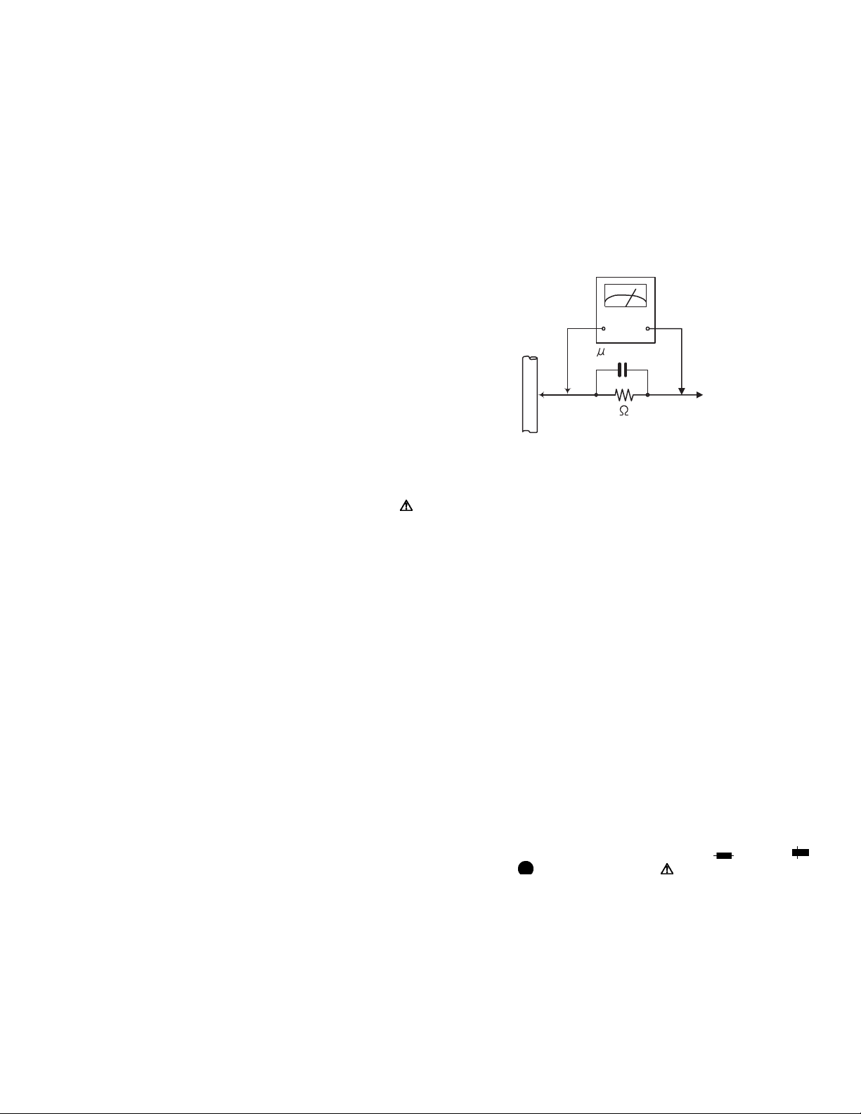
(5) Leakage shock hazard testing
After reassembling the product, always perform an isolation check on the exposed metal parts of the product (antenna terminals, knobs, metal cabinet, screw heads,
headphone jack, control shafts, etc.) to be sure the product
is safe to operate without danger of electrical shock.Do not
use a line isolation transformer during this check.
• Plug the AC line cord directly into the AC outlet. Using a
"Leakage Current Tester", measure the leakage current
from each exposed metal parts of the cabinet, particularly any exposed metal part having a return path to the
chassis, to a known good earth ground. Any leakage current must not exceed 0.5mA AC (r.m.s.).
• Alternate check method
Plug the AC line cord directly into the AC outlet. Use an
AC voltmeter having, 1,000Ω per volt or more sensitivity
in the following manner. Connect a 1,500Ω 10W resistor
paralleled by a 0.15µF AC-type capacitor between an ex-
posed metal part and a known good earth ground.
Measure the AC voltage across the resistor with the AC
voltmeter.
Move the resistor connection to each exposed metal
part, particularly any exposed metal part having a return
path to the chassis, and measure the AC voltage across
the resistor. Now, reverse the plug in the AC outlet and
repeat each measurement. Voltage measured any must
not exceed 0.75 V AC (r.m.s.). This corresponds to 0.5
mA AC (r.m.s.).
AC VOLTMETER
(Having 1000
ohms/volts,
or more sensitivity)
0.15 F AC TYPE
Place this
probe on
1500 10W
Good earth ground
1.2 Warning
(1) This equipment has been designed and manufactured to
meet international safety standards.
(2) It is the legal responsibility of the repairer to ensure that
these safety standards are maintained.
(3) Repairs must be made in accordance with the relevant
safety standards.
(4) It is essential that safety critical components are replaced
by approved parts.
(5) If mains voltage selector is provided, check setting for local
voltage.
1.3 Caution
Burrs formed during molding may be left over on some parts
of the chassis.
Therefore, pay attention to such burrs in the case of preforming repair of this system.
1.4 Critical parts for safety
In regard with component parts appearing on the silk-screen
printed side (parts side) of the PWB diagrams, the parts that are
printed over with black such as the resistor ( ), diode ( )
and ICP ( ) or identified by the " " mark nearby are critical
for safety. When replacing them, be sure to use the parts of the
same type and rating as specified by the manufacturer.
(This regulation dose not Except the J and C version)
each exposed
metal part.
(No.MA475<Rev.001>)1-5
Page 6
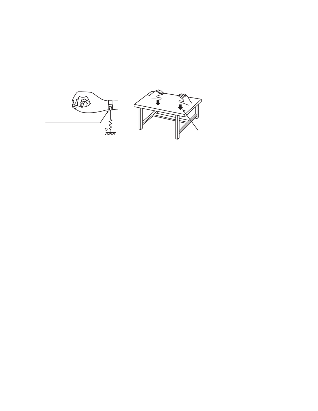
1.5 Preventing static electricity
Electrostatic discharge (ESD), which occurs when static electricity stored in the body, fabric, etc. is discharged, can destroy the laser
diode in the traverse unit (optical pickup). Take care to prevent this when performing repairs.
1.5.1 Grounding to prevent damage by static electricity
Static electricity in the work area can destroy the optical pickup (laser diode) in devices such as laser products.
Be careful to use proper grounding in the area where repairs are being performed.
(1) Ground the workbench
Ground the workbench by laying conductive material (such as a conductive sheet) or an iron plate over it before placing the
traverse unit (optical pickup) on it.
(2) Ground yourself
Use an anti-static wrist strap to release any static electricity built up in your body.
(caption)
Anti-static wrist strap
1M
Conductive material
(conductive sheet) or iron palate
(3) Handling the optical pickup
• In order to maintain quality during transport and before installation, both sides of the laser diode on the replacement optical
pickup are shorted. After replacement, return the shorted parts to their original condition.
(Refer to the text.)
• Do not use a tester to check the condition of the laser diode in the optical pickup. The tester's internal power source can easily
destroy the laser diode.
1.6 Handling the traverse unit (optical pickup)
(1) Do not subject the traverse unit (optical pickup) to strong shocks, as it is a sensitive, complex unit.
(2) Cut off the shorted part of the flexible cable using nippers, etc. after replacing the optical pickup. For specific details, refer to the
replacement procedure in the text. Remove the anti-static pin when replacing the traverse unit. Be careful not to take too long a
time when attaching it to the connector.
(3) Handle the flexible cable carefully as it may break when subjected to strong force.
(4) I t is not possible to adjust the semi-fixed resistor that adjusts the laser power. Do not turn it.
1-6 (No.MA475<Rev.001>)
Page 7
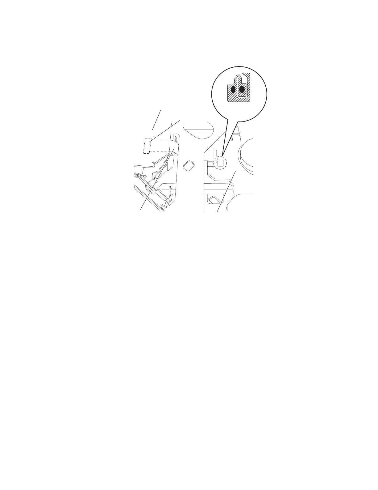
1.7 Attention when traverse unit is decomposed
*Please refer to "Disassembly method" in the text for the pickup unit.
• Apply solder to the short land sections before the card wire is disconnected from the connector on the servo board. (If the card wire
is disconnected without applying solder, the pickup may be destroyed by static electricity.)
• In the assembly, be sure to remove solder from the short land sections after connecting the card wire.
Mechanism control board
CN102
Flexible wire
Short land section
Pickup
(No.MA475<Rev.001>)1-7
Page 8
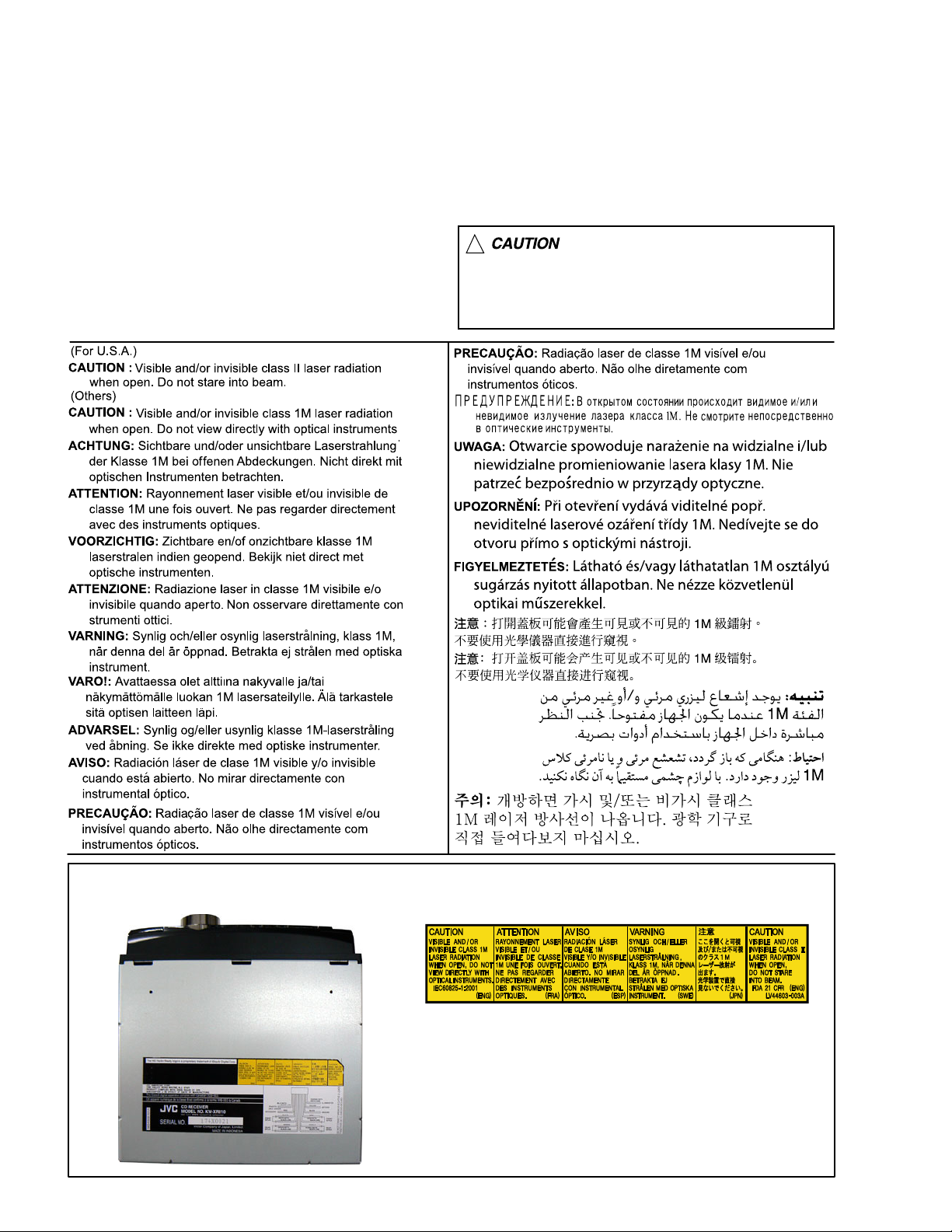
1.8 Important for laser products
1.CLASS 1 LASER PRODUCT
2.CAUTION :
(For U.S.A.) Visible and/or invisible class II laser radiation
when open. Do not stare into beam.
(Others) Visible and/or invisible class 1M laser radiation
when open. Do not view directly with optical instruments.
3.CAUTION : Visible and/or invisible laser radiation when
open and inter lock failed or defeated. Avoid direct
exposure to beam.
4.CAUTION : This laser product uses visible and/or invisible
laser radiation and is equipped with safety switches which
prevent emission of radiation when the drawer is open and
the safety interlocks have failed or are defeated. It is
dangerous to defeat the safety switches.
5.CAUTION : If safety switches malfunction, the laser is able
to function.
6.CAUTION : Use of controls, adjustments or performance of
procedures other than those specified here in may result in
hazardous radiation exposure.
!
Please use enough caution not to
see the beam directly or touch it
in case of an adjustment or operation
check.
REPRODUCTION AND POSITION OF LABELS and PRINT
WARNING LABEL and PRINT
1-8 (No.MA475<Rev.001>)
Page 9
SECTION 2
SPECIFIC SERVICE INSTRUCTIONS
This service manual does not describe SPECIFIC SERVICE INSTRUCTIONS.
SECTION 3
DISASSEMBLY
3.1 Main body (Used model: KW-XR610)
3.1.1 Removing the Front panel (See Fig.1)
(1) Remove the two screws A attaching the both side of the
Front panel.
(2) Disengage four hooks a engaged both side of the Front
panel.
A hook a
Fig.1
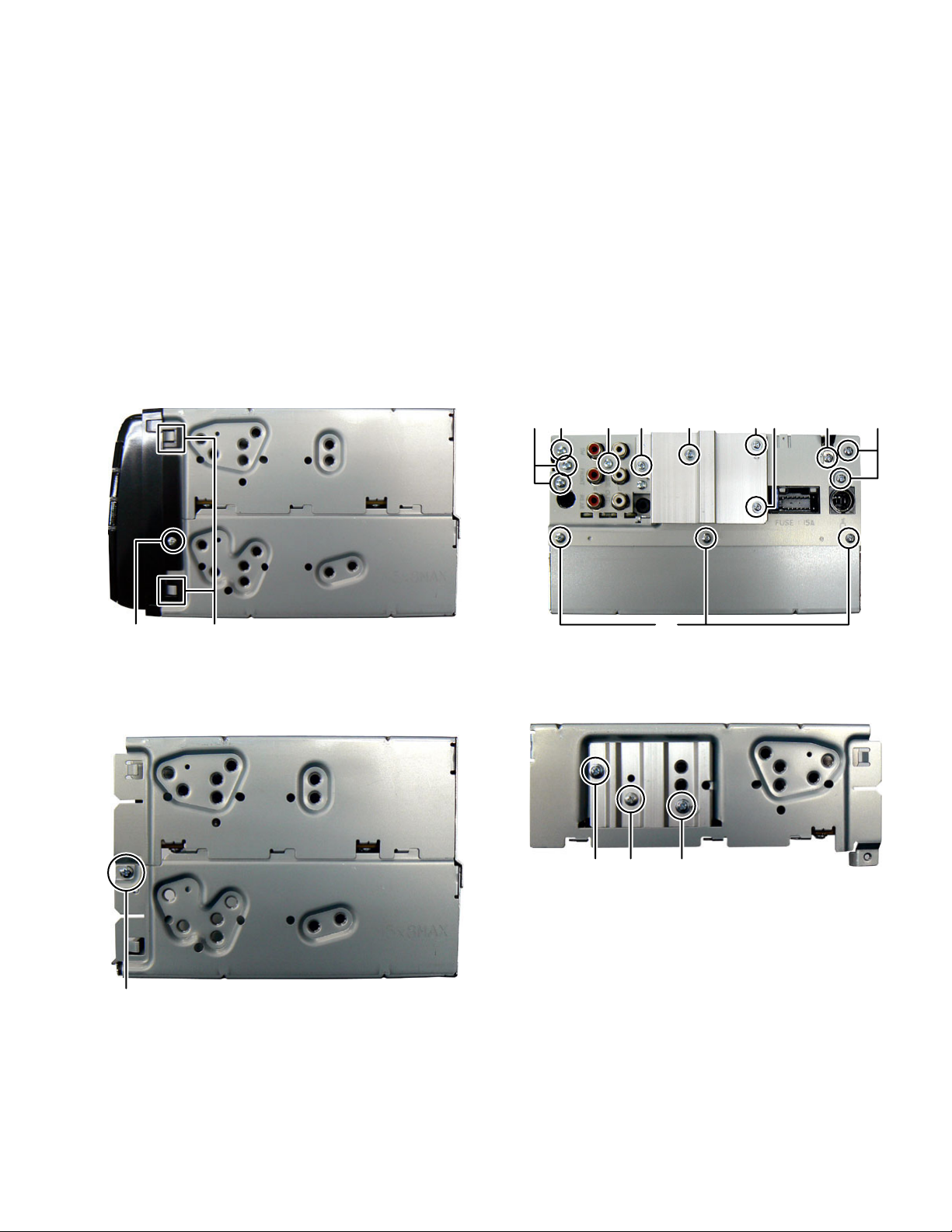
3.1.2 Removing the Bottom chassis (See Fig.2, 3)
(1) Remove the two screws B attaching the both side of the
Bottom chassis. (See Fig.2)
(2) Remove the three screws C attaching the Bottom chassis.
(See Fig.3)
(3) Remove the three screws D and one screw E attaching the
Heat sink. (See Fig.3)
(4) Remove the six screws F and one screw G attaching the
Rear bracket. (See Fig.3)
DDFFFFGDE
C
Fig.3
3.1.3 Removing the Main board (See Fig.4, 5)
(1) Remove the two screws H and one screw J attaching the
Side plate. (See Fig.4)
B
HHJ
Fig.4
Fig.2
(No.MA475<Rev.001>)1-9
Page 10
(2) Remove the three screws K attaching the Main board. (See
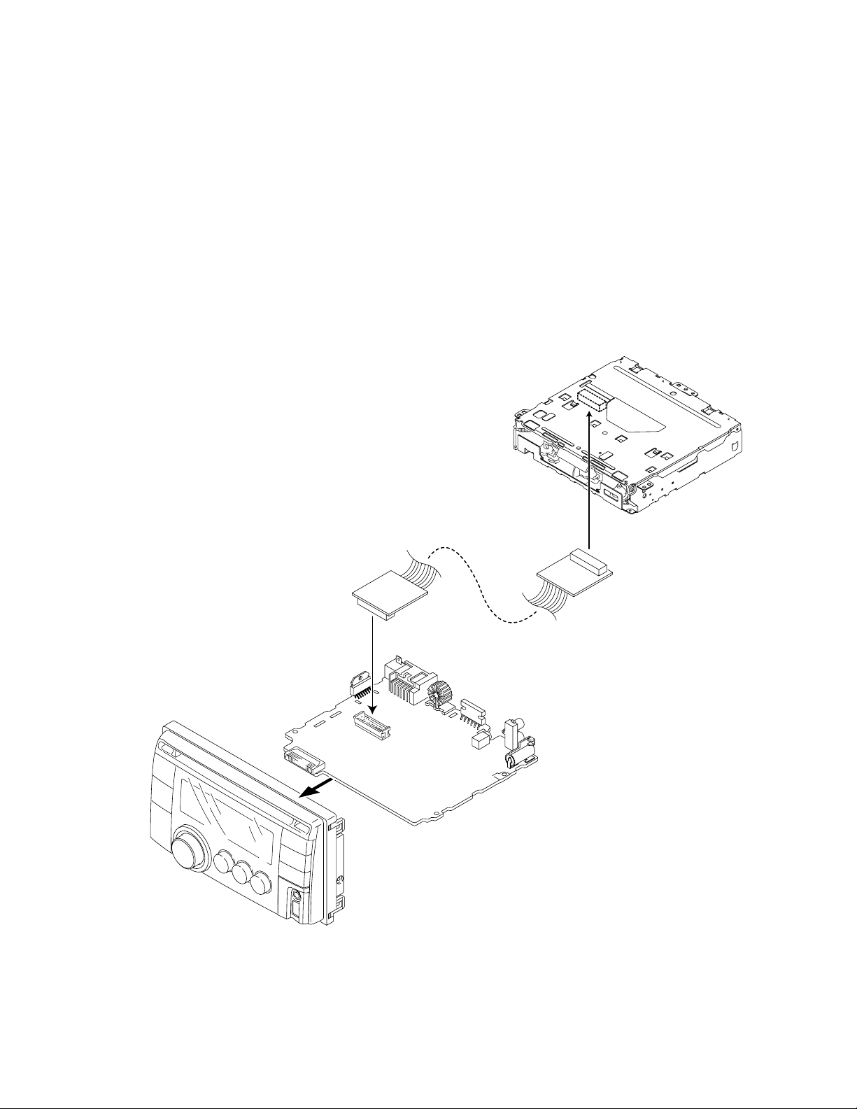
Fig.5)
(3) Disconnect B-B connector CN501
nected the CD mechanism and Main board. (See Fig.5)
of the Main board con-
K
CN501
Fig.5
3.1.4 Removing the CD mechanism (See Fig.6)
(1) Remove the three screws L attaching the CD mechanism.
L
K
L
Fig.6
3.1.5 Removing the Switch board (See Fig.7)
(1) Remove the Volume knob.
(2) Disconnect the flexible wire from LCD connected to con-
nector CN602
(3) Remove the sixteen screws M attaching the Switch board.
of the Switch board.
CN602
M
M
Fig.7
M
1-10 (No.MA475<Rev.001>)
Page 11
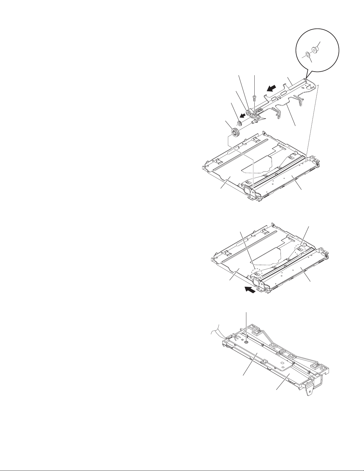
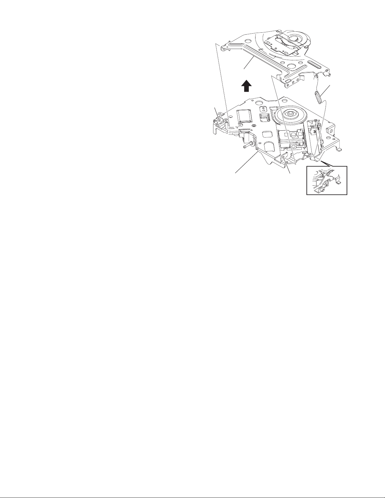
3.2 CD MECHANISM assembly section
• Remove the CD MECHANISM assembly from the main body.
3.2.1 Removing the MECHANISM CONTROL BOARD as-
sembly (See Fig.1 and 2
(1) From the bottom side of CD MECHANISM assembly, re-
move the solders from the soldered sections (a, b and c)
on the MECHANISM CONTROL BOARD assembly. (See
Fig.1.)
(2) Remove the three screws A and one screw B attaching the
MECHANISM CONTROL BOARD assembly. (See Fig.1.)
(3) Solder the short land sections on the pickup. (See Fig.2.)
Caution:
• Solder the short land sections on the pickup before
disconnecting the flexible wire from the connector
on the MECHANISM CONTROL BOARD as-
CN102
sembly.
If the card wire is disconnected without attaching
solder, the pickup may be destroyed by static
electricity. (See Fig.2.)
• When attaching the MECHANISM CONTROL BOARD
assembly, remove the solders from the short land sections after connecting the flexible wire to the connector
on the MECHANISM CONTROL BOARD as-
CN102
sembly.
)
Mechanism
control board
a
A
A
Fig.1
b
CN102
B
A
c
Mechanism control board
CN102
Flexible wire
Short land section
Pickup
Fig.2
(No.MA475<Rev.001>)1-11
Page 12
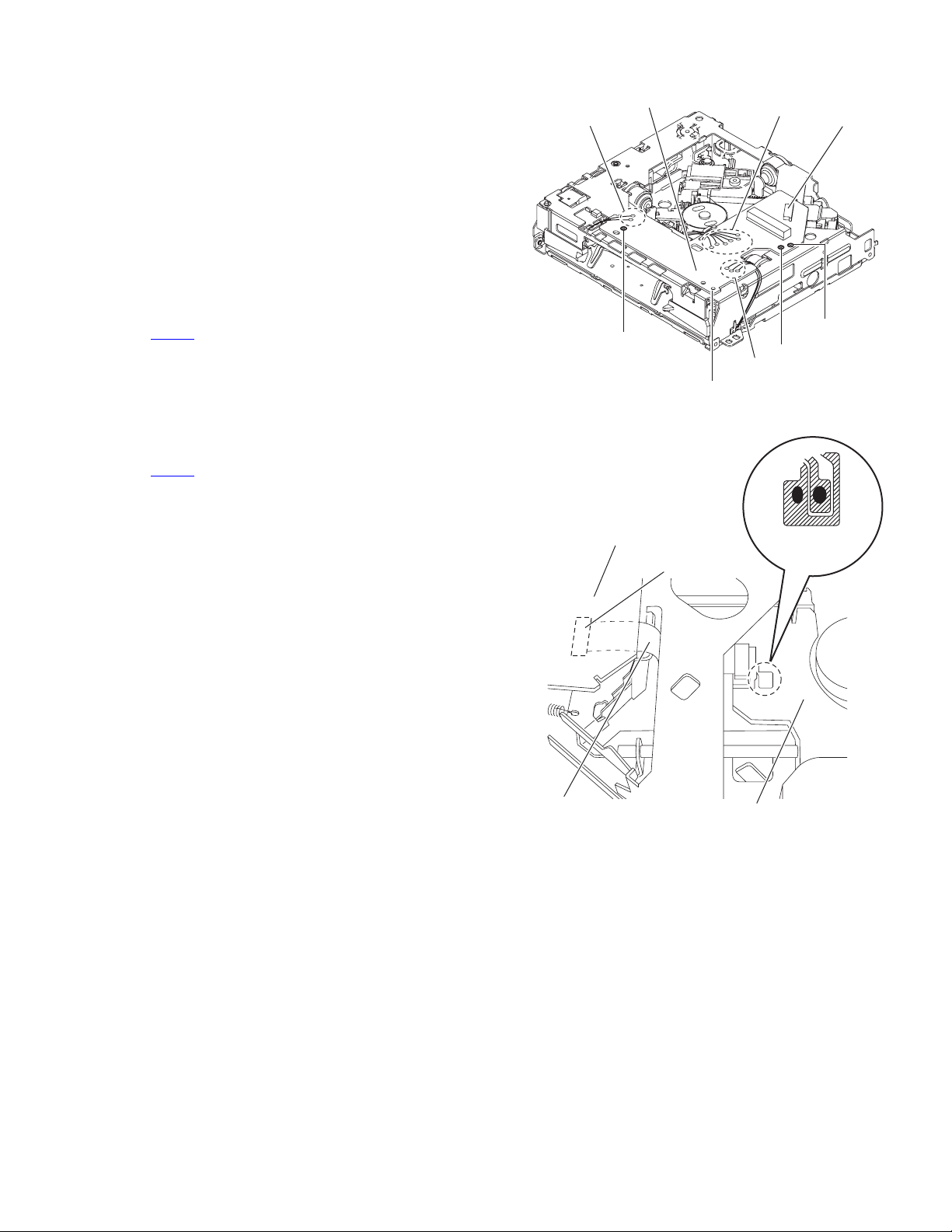
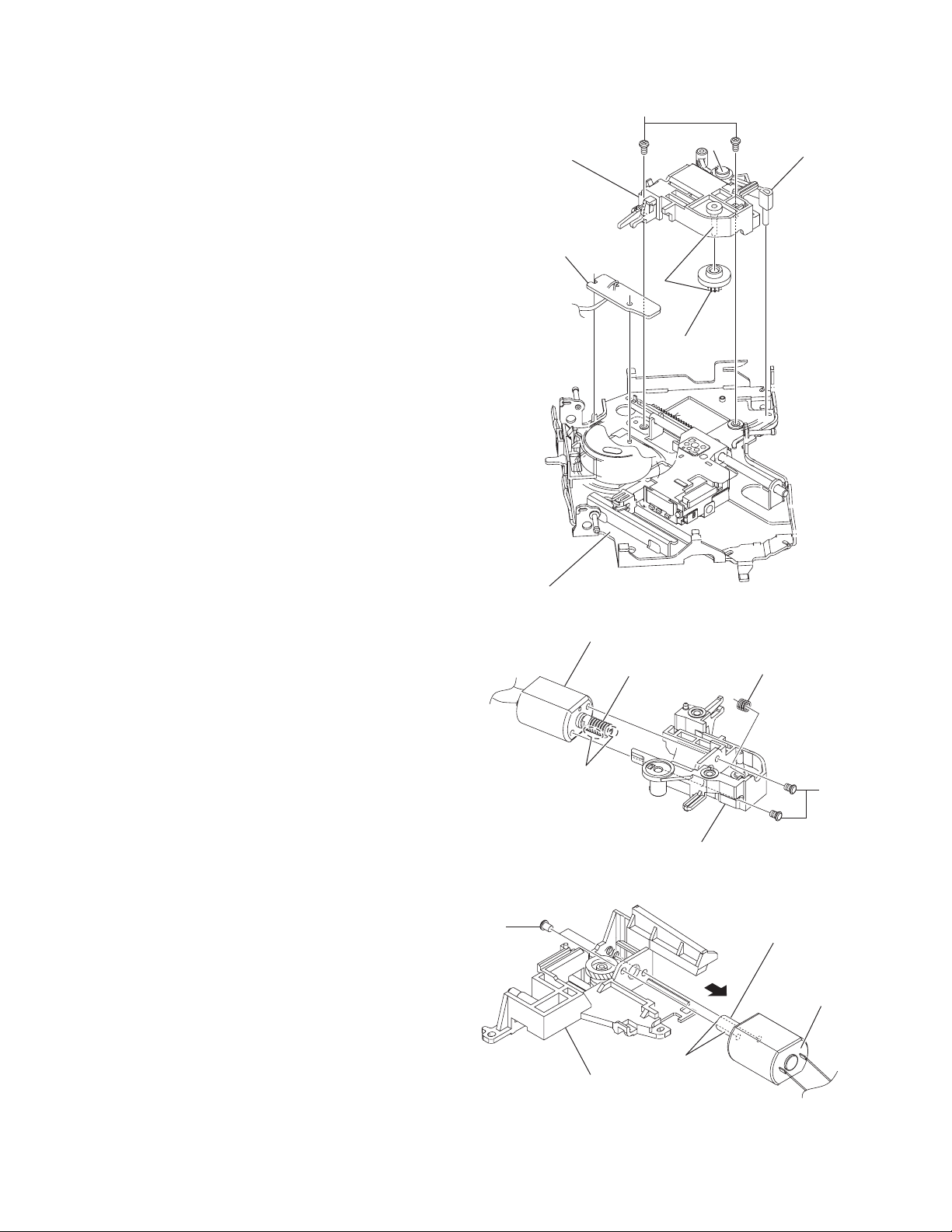
3.2.2 Removing the top cover (See Fig.3 to 5)
• Remove the MECHANISM CONTROL BOARD assembly.
(1) From the front side of the CD MECHANISM assembly,
change the hook position of the two roller springs. (See
Fig.3.)
(2) From the side of the CD MECHANISM assembly, remove
the six screws C attaching the top cover. (See Fig.3 and 4.)
(3) Take out the top cover in an upward direction. (See Fig.5.)
Top cover
C
Top cover
Fig.5
Roller spring Roller spring
Fig.3
Top cover
C
Fig.4
C
1-12 (No.MA475<Rev.001>)
Page 13
3.2.3 Removing the roller (See Fig.6)
• Remove the MECHANISM CONTROL BOARD assembly and
top cover.
(1) From the bottom side of the top cover, remove the screw D
attaching the gear holder.
(2) Remove the R.holder assembly from disc plate, and then
take out the roller from R.holder assembly in the direction
of the arrow.
Reference:
When attaching the R.ACT gear (2) and R.ACT gear (3),
apply grease to the section d of R.holder assembly.
Gear holder
Roller gear
R.ACT gear(3)
D
Roller coller
Washer
Roller
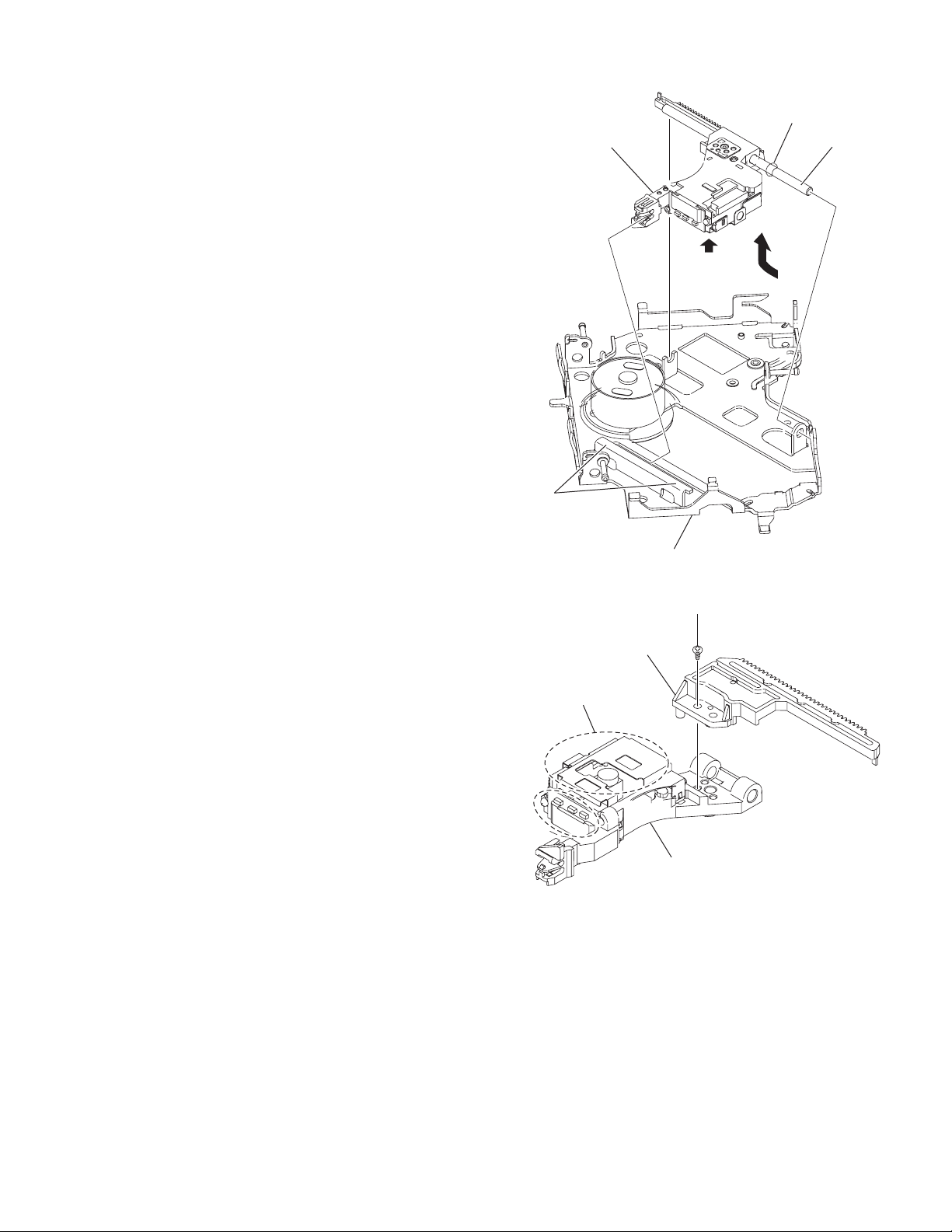
3.2.4 Removing the PHOTO BOARD assembly (See Fig.7 and 8)
• Remove the MECHANISM CONTROL BOARD assembly and
top cover.
From the bottom side of the top cover, release the
(1)
projection
7
Fig.
(2) Take out the disc plate in the direction of the arrow. (See
Fig.7.)
(3) From the reverse side of the disc plate, remove the screw
E attaching the PHOTO BOARD assembly. (See Fig.8.)
e
from the notch of the disc plate. (See
.)
R.ACT gear(2)
Top cover
Top cover
d
R.holder assembly
Disc plate
Fig.6
e
e
Disc plate
E
Photo board
Fig.7
Disc plate
Fig.8
(No.MA475<Rev.001>)1-13
Page 14
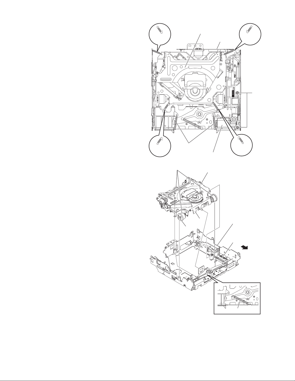
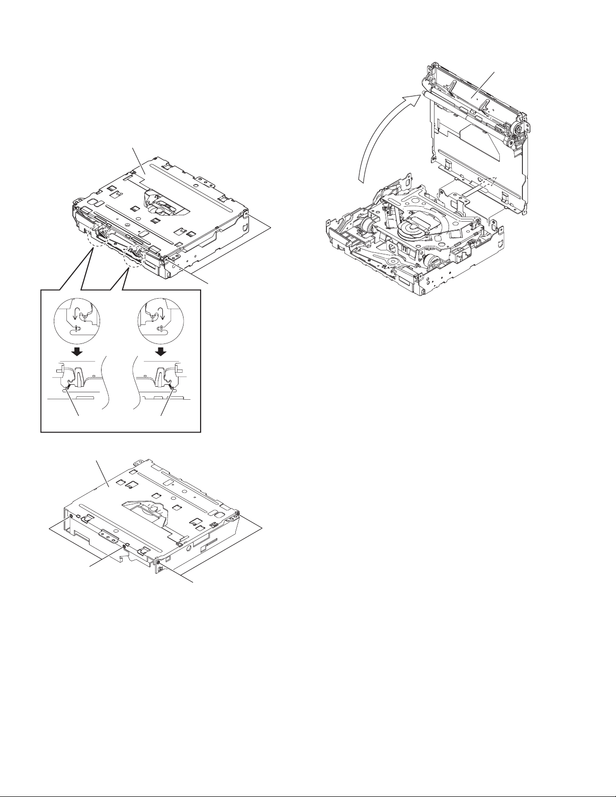
3.2.5 Removing the mechanism section (See Fig.9 and 10)
• Remove the MECHANISM CONTROL BOARD assembly and
top cover.
(1)
From the top side of the CD MECHANISM assembly,
F
remove the two screws
assembly. (See Fig.
(2) Remove the two roller springs on the top side of the mecha
frame. (See Fig.9.)
(3) Remove the four SUS springs on the top side of the mecha
frame. (See Fig.9.)
(4) Remove the link spring on the top side of the mecha frame.
(See Fig.10.)
(5) Release section f of the three dampers from the mecha
frame. (See Fig.10.)
Reference:
When attaching the roller spring and SUS spring, keep
direction before remove.
Move the slide cam (R) assembly in the direction of the
(6)
arrow, and then take out the mechanism section in an
upward direction. (See Fig.10.)
Reference:
When attaching the mechanism section, apply grease to
the section g. (See Fig.10.)
attaching the loading motor
9
.)
SUS
spring
SUS
spring
Mechanism section
Roller spring
Loading motor assembly
Fig.9
Damper
Mechanism section
Mecha frame
SUS
spring
F
SUS
spring
g
f
Fig.10
Mecha frame
Slidecam(R)
assembly
Link spring
1-14 (No.MA475<Rev.001>)
Page 15
3.2.6 Removing the slide cam (L) (See Fig.11 to 13)
• Remove the MECHANISM CONTROL BOARD assembly, top
cover and mechanism section.
(1) From the top side of the mecha frame, remove the screw G
attaching the cam cover. (See Fig.11.)
Take out the cam cover from mecha frame in an upward
(2)
11
G
.)
Cam cover
direction. (See Fig.
(3) Take out the slide cam (L) in the direction of the arrow.
(See Fig.12.)
Reference:
When attaching the slide cam (L), apply grease to the
section h. (See Fig.13.)
h
Slide cam(L)
h
h
h
h
Slide cam(L)
h
Fig.13
h
h
Mecha frame
Slide cam(L)
Fig.11
Mecha frame
Fig.12
(No.MA475<Rev.001>)1-15
Page 16
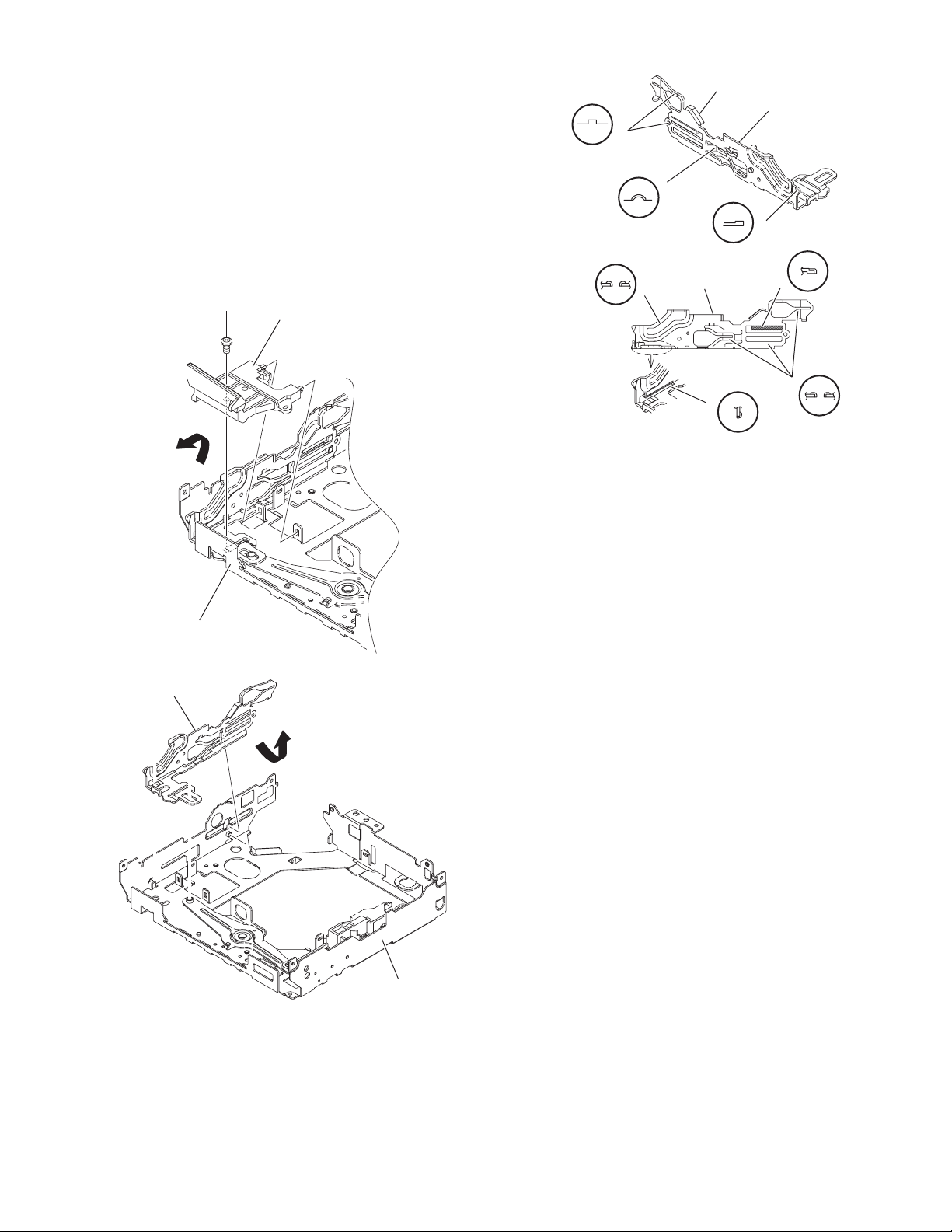
3.2.7 Removing the F.lock lever and slide cam (R) (See
Fig.14 and 15)
• Remove the MECHANISM CONTROL BOARD assembly, top
cover and mechanism section.
(1) From the top side of the mecha frame, take out the slide
cam (R) assembly in an upward direction. (See Fig.14.)
(2) Rotate the F.lock lever in the direction of the arrow 1, and
then take out the direction of the arrow 2. (See Fig.14.)
Reference:
When attaching the slide cam (R) assembly, the f.lock
lever and the link arm apply grease to the section
14
(See Fig.
and 15.)
h
Slide cam(R) assembly
h
F.lock lever
2
1
h
.
h
Mecha frame
h
h
Fig.14
Link arm
h
Slide cam(R) assembly
h
h
h
3.2.8 Removing the damper (See Fig.16)
• Remove the MECHANISM CONTROL BOARD assembly, top
cover and mechanism section.
From the mechanism section, pull out the three dampers in the
direction of the arrow.
Reference:
Before inserting the shaft to the dampers, apply IPA to the
pocket j of damper.
h
h
h
Slide cam(R) assembly
Fig.15
Damper (Gray)
Damper (Brown)
j
j
1-16 (No.MA475<Rev.001>)
Damper (Brown)
j
Fig.16
Page 17
3.2.9 Removing the clamper assembly (See Fig.17)
• Remove the MECHANISM CONTROL BOARD assembly, top
cover and mechanism section.
(1) From the top side of the mechanism section, release the
clamper spring.
(2) Move the clamper assembly in the direction of the arrow,
and then release the joints (k and m).
Take out the clamper assembly from the T.M chassis
(3)
assembly.
Clamper assembly
Clamper spring
k
T.M. chassis assembly
m
Fig.17
(No.MA475<Rev.001>)1-17
Page 18
3.2.10 Removing the feed motor (See Fig.18 and 19)
r
• Remove the MECHANISM CONTROL BOARD assembly, top
cover, mechanism section and clamper assembly.
(1) From the bottom side of the T.M chassis assembly, remove
the two screws H attaching the feed motor assembly. (See
Fig.18.)
Remove the two screws J attaching the feed motor to
(2)
19
f.motor holder. (See Fig.
Reference:
When attaching the f. wheel gear, trigger arm and feed
motor, apply grease to the sections (n, p and q). (See
Fig.18 and 19.)
3.2.11 Removing the SWITCH BOARD assembly (See
Fig.18)
• Remove the MECHANISM CONTROL BOARD assembly, top
cover, mechanism section, clamper assembly and feed motor
assembly.
From the bottom side of the T.M chassis assembly, take out
the SWITCH BOARD assembly in an upward direction from
T.M chassis assembly.
.)
Feed motor assembly
Switch board
H
n
F.wheel gear
p
Trigger arm
3.2.12 Removing the loading motor (See Fig.20)
• Remove the MECHANISM CONTROL BOARD assembly, top
cover, mechanism section and clamper assembly.
(1) From the right side of the L.M base assembly, remove the
two screws K attaching the loading motor.
(2) Take out the loading motor in the direction of the arrow
from the L.M base assembly.
Reference:
When attaching the loading motor, apply grease to the
section r.
T.M. chassis assembly
Feed motor
F.worm gear
q
K
L.M. base assembly
Fig.18
Comp. spring
J
F.motor holder
Fig.19
L.worm gear
Loading moto
r
1-18 (No.MA475<Rev.001>)
Fig.20
Page 19
3.2.13 Removing the pickup assembly (See Fig.21 to 22)
• Remove the MECHANISM CONTROL BOARD assembly, top
cover, mechanism section, clamper assembly and feed motor
assembly.
Caution:
• Do not touch section u on the pickup assembly. (See Fig.21
and 22.)
(1) From the bottom side of the T.M chassis assembly, move
the pickup assembly in the direction of the arrow from the
T.M chassis assembly. (See Fig.21.)
(2) Pull out the main shaft. (See Fig.21.)
(3) Remove the screw M attaching the pickup to the rack plate.
(See Fig.22.)
Reference:
When attaching the loading motor, apply grease to the
sections s and t. (See Fig.21.)
Pick up assembly
s
t
Main shaft
u
T.M. chassis assembly
Rack plate
u
Pick up
Fig.21
M
Fig.22
(No.MA475<Rev.001>)1-19
Page 20
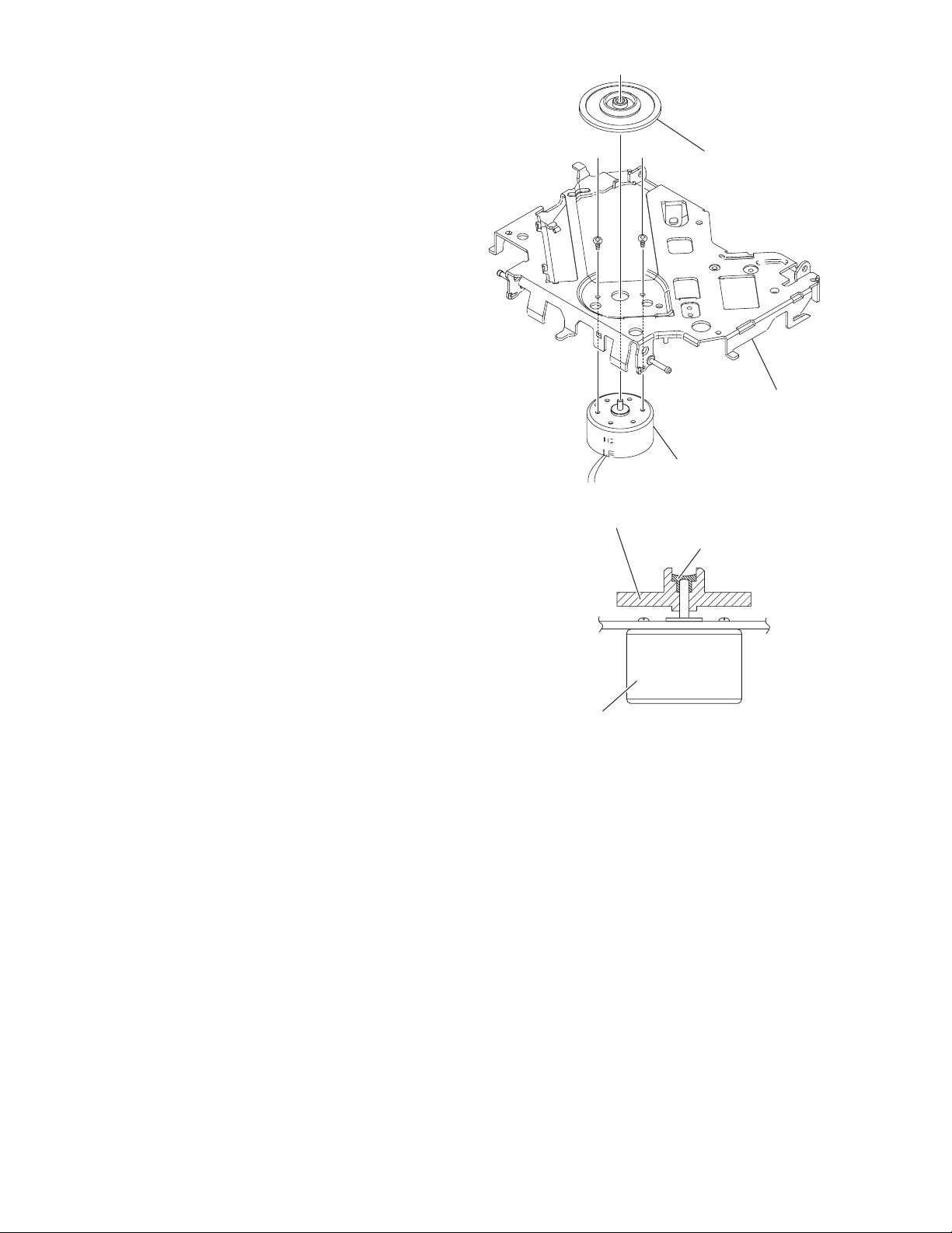
3.2.14 Removing the spindle motor (See Fig.23 and 24)
•
Remove the MECHANISM CONTROL BOARD assembly,
top cover, mechanism section, clamper assembly, feed motor
assembly and pickup assembly.
(1) From the top side of the T.M chassis assembly, remove the
CD T.table assembly from the spindle motor. (See Fig.23.)
(2) Remove the two screws N attaching the spindle motor.
(See Fig.23.)
(3) Take out the spindle motor from the bottom side of the T.M
chassis assembly. (See Fig.23.)
Reference:
When attaching the CD T.table assembly to the spindle
motor shaft, apply loctite 460 to inside the CD T.table
assembly. (See Fig.24.)
NN
Spindle motor
Fig.23
CD T.table assembly
CD T.table assembly
T.M.chassis assembly
Loctite
Spindle motor
Fig.24
1-20 (No.MA475<Rev.001>)
Page 21
SECTION 4
ADJUSTMENT
4.1 Test instruments required for adjustment
(1) Digital oscilloscope (100MHz)
(2) Digital tester
(3) Test Disc
(4) Extension cable : EXTGS004-26PL
4.2 Standard measuring conditions
Power supply voltage DC14.4V(10.5 to 16V)
Load impedance 20K ohm (2 Speakers connection)
Output Level Line out 2.5V (Vol. MAX)
4.5 How to connect the extension cable for adjusting
Caution:
Be sure to attach the heat sink and rear bracket onto the power amplifier IC and regulator IC respectively, before supply the power.
If voltage is applied without attaching these parts, the power amplifier IC and regulator IC will be destroyed by heat.
4.3 Standard volume position
Balance and Bass &Treble volume : lndication"0"
Loudness : OFF
4.4 Dummy load
Exclusive dummy load should be used for AM,and FM.
For FM dummy load, there is a loss of 6dB between SSG output
and antenna input.
The loss of 6dB need not be considered sincedirect reading of
figures are applied in this working standard.
Extension cable
EXTGS004-26PL
(No.MA475<Rev.001>)1-21
Page 22

4.6 Service Mode
4.6.1 Service mode setting
(1) Push POWER BUTTON (Power ON)
(2) Set to service mode
Keep this state more 3 seconds while connecting pressing the [MENU] button and [] button sequentially.
(3) Select the menu with [VOL -] and [VOL+], and decide it with [Enter] button.
(4) When the [BACK] button is pushed, it returns to the former menu.
Service mode (MENU)
Service Mode
Data Clear
Tuner Service Mode
CD Service mode
Bluetooth Version
HD Service Mode
Rom correction Mode
Service mode
Version
MAIN ****
HD V***
CH V***
Error Read
OK: Function
CD Data Read
OK: Function
Data Clear
Initialize All
Name Clear
CD Error Clear
USB Error Clear
CH Error Clear
Init Bluetooth
Init HD Radio
Tuner Service Mode
VER=#***
TINJ=**
##**
#####
SPI=####
PI =####
TP =#TA=*
AF=####
LEV=##H
IFC=##H
RFAGC=##
RDS Engineer Mode
VOL PUSH: Enter
Panel V***
USB V***
R **-**
########
########
PTY=##
MS =#DI=*
**** $$$
U&W=##H
IFBW=#
IFAGC=##
MAIN: Main micon version Panel: Panel micon version
HD : HD radio version USB : USB micon version
CH : CH version R : Panel micon ROM version
CD Error Read
USB Error Read
CH Error Read
Total Error :****
E1 ******
E2 ******
1 ******
2 ******
3 ******
ADJ NOW
ADJ INT
OTHERS
FEB *** FEO*** TEB***
FGA *** TEO*** TGA***
RFG ***
IOP TEMP I**T
TEMP MAX*** IOP INT**
P TOTAL ****H
TUR=## - - **
TUW=## - - **
F/A-LEV=******
F/A-USN=******
F/A-WAM=******
F/A-IFC=******
F-LV1=******
IF-BW=******
SKTM=******
RDTM=******
##** ########
#####
E3 ******
4 ******
5 ******
ADJ NOW
ADJ INT
OTHERS
CD Service Mode
FEBC =**
TEBC =**
FEOF =**
RFGC=**
JPTRM=**
RFRP=**
TEPK=**
DMO=**
Bluetooth Version
SW BT_CORE ***
HW BT_MODULE ***
SW BT_MODULE ***
ADR-*******
HD Service Mode
(It is displayed in HD Radio Tuner connection.)
SM **
IDM V***
MP **
ADJ **
IFBW *
IF ******
QI **
SNR **
BCNT *
AGAIN **
SPROC **
Rom correction Mode : Rom corre version
FGADD=**
TGADD=**
TEOF =**
SPOFF=**
JPTRL=**
TRLPF=**
TEBT=**
1-22 (No.MA475<Rev.001>)
Page 23

4.6.2 Mechanical Error Detail Codes
Condition Details Error Code Detail Code
Disc Loading Error
(1) B1 Time Out After detecting SW1=L, it does not become SW2=L 09 0011
(2) B2 Time Out After detecting SW2=H, it does not become SW2=L 09 0012
(3) C1 Time Out After detecting SW2=L, it does not become SW2=H 09 0013
Eject Error
(1) B1 Time Out After detecting SW2=H, it does not become SW2=L 01 0021
(2) C2 Time Out After detecting SW2=L, it does not become SW2=H 01 0022
(3) B2 Time Out After detecting SW1=L, it does not become SW2=L
immediately after RESET and so on.
(4) D0 Panel Close Disc can not be ejected due to closed panel. 01 0024
Forced Eject Error
(1) E1 Error SW1=H, SW2=L detected from NO DISC 01 0041
(2) E2 Error Detected SW1=L after RESET, and then detected SW1=H 01 0042
(3) E3 Error Detected SW1=H after RESET 01 0043
(4) E4 Error Detected SW1=H after SW1=L 01 0044
(5) E5 Error Detected SW1=H after SW2=H→L010045
(6) E6 Error Time Out for Loading after RESET 01 0046
(7) E7 Error Detected SW1=H after SW2=H→L→H010047
(8) E8 Error Eject Key input while the procedure is not completed after 01 0048
Forced Eject execution
(9) E9 Error Eject Key input during Disc is on the way and not completed 01 0049
Loading Waiting Error
(1) SW1=H or NO DISC
detection before Loading
Motor activation during
Disc is waiting at the
waiting location.
(2) SW2=L before Loading
Motor activation during
Disc is waiting at the
waiting location.
Disc is removed or NO DISC detection condition 09 0031
Disc is inserted 09 0032
01 0023
(No.MA475<Rev.001>)1-23
Page 24

5.1 16 PIN CORD DIAGRAM (For KW-XR810)
8
GN/BK
7
VI/BK GY/BK
6
5
VI GY
NC
WHGN
WH/BK
NC
SECTION 5
TROUBLESHOOTING
Black
9
10
11
12
134
BK
RD
BL
WH
VI
Red
Blue
White
Violet
GN
GY
YL
Green
Gray
OrangeOR
Yellow
BK
1
YL
16
OR/WH
15
RD
2
GN
8
GN/BK
7
VI
5
3
2
1
BL/WH
RD
BK
NC
OR/WH
YL
14
15
16
VI/BK
6
WH
9
WH/BK
10
GY
12
GY/BK
11
BL/WH
3
1-24 (No.MA475<Rev.001>)
Page 25

5.2 16 PIN CORD DIAGRAM (For KW-XR811, KW-XR817)
8
7
GN/BK
6
VI/BK GY/BK
5
VI GY
NC
3
BL/WH
WHGN
WH/BK
NC
NC
9
10
11
12
134
14
BK
RD
BL
WH
VI
Black
Red
Blue
White
Violet
GN
GY
YL
Green
Gray
OrangeOR
Yellow
2
16
15
1
3
8
2
1
RD1
YL1
OR/WH
BK
BL/WH
GN
RD
BK
OR/WH
YL
15
16
RD2
RD3
YL2
7
4
6
8
5
7
3
5
7
NC
BL/WH
RD 3
NC NC
1
2
4
YL 2
6
OR/WH
8
BK
7
5
6
9
10
12
11
GN/BK
VI
VI/BK
WH
WH/BK
GY
GY/BK
8
1
2
5
1
VI
GY
3
6
3
4
(No.MA475<Rev.001>)1-25
WH
5
7
GN
2
VI/BK
4
GY/BK
6
WH/BK
8
GN/BK
Page 26

5.3 16 PIN CORD DIAGRAM (For KW-XR611)
1
16
4
3
8
GN/BK
7
6
5
BL/WH
3
2
1
BK
YL
BL
BL/WH
WHGN
WH/BK
VI/BK GY/BK
VI GY
NC
RD
BK
NC
NC
OR/WH
YL
9
10
11
12
134
14
15
16
BK
RD
BL
WH
VI
Black
Red
Blue
White
Violet
GN
GY
YL
Green
Gray
OrangeOR
Yellow
RD
2
OR/WH
15
GN
8
GN/BK
7
VI
5
VI/BK
6
WH
9
WH/BK
10
GY
12
GY/BK
11
1-26 (No.MA475<Rev.001>)
Page 27

Page 28

Victor Company of Japan, Limited
Mobile Entertainment Division 10-1,1chome,Ohwatari-machi,Maebashi-city,371-8543,Japan
(No.MA475<Rev.001>)
Printed in Japan
VSE
Page 29

SCHEMATIC DIAGRAMS
21
CD RECEIVER
KW-XR810JKW-XR816UKW-XR816UH
KW-XR811EKW-XR811EYKW-XR811EU
KW-XR817EE
(No.MA475<Rev.001>)1/
Page 30

■ PRECAUTIONS ON SCHEMATIC DIAGRAMS
z Due to the improvement in performance, some part numbers shown in the circuit diagrams
may not agree with those indicated in the Parts List.
z The parts numbers, values and rated voltage etc. in the Schematic Diagrams are for
reference only.
z Since the circuit diagrams are standard ones, the circuits and circuit constants may be
subject to change for improvement without any notice.
■ PRECAUTIONS ON PARTS LIST
z
The parts identified by the symbol are critical for safety. Whenever replacing these parts, be sure to
use specified ones to secure the safety.
z
The parts not indicated in this Parts List and those which are filled with lines --- in the Parts No.
columns will not be supplied.
z
P.W. BOARD Ass'y will not be supplied, but those which are filled with the Parts No. in the Parts No.
columns will be supplied.
z
When ordering chips, screws etc., place bulk orders (unit of tens) whenever possible to improve
shipping efficiency.
z
There are cases where the actual implemented parts in the sets and the service parts are different.
When ordering parts, make sure to refer to the Parts List.
■
PRECAUTIONS ON SERVICE
Certain parts of the power circuits and the GNDs differ according to the models. Care must be
taken for the following points as the differences are indicated separately in the LIVE GND ( ) and
the ISOLATED (NEUTRAL) GND ( ).
1. Do not touch the LIVE GND, or do not touch the LIVE GND and the ISOLATED (NEUTRAL)
GND at the same time. It may cause an electric shock.
Before pulling out the chassis or other parts, make sure to pull out the power cord from the
wall outlet first.
2. Do not short circuit between the LIVE GND and ISOLATED (NEUTRAL) GND, or never
measure the LIVE GND and ISOLATED (NEUTRAL) GND at the same time using measuring
instruments (oscilloscope, etc.). It may blow fuses or damage other parts.
■ DEVIATION TOLERANCE RANGE
DEVIATION TOLERANCE RANGE
F G J K M N R H Z P
± 1% ± 2% ± 5% ±10% ±20% ±30%
+30%
-10%
+50%
-10%
+80%
-20%
+100%
-0%
21
(No.MA475<Rev.001>)2/
Page 31

Q852Q851
Q785
Q784
Q781
Q201
Q101
,
,
,
,
Q977
Q976
PS2
DIMMER INPUT
Q881
AUTO
ANTENNA
MUTE CONTROL
Q782
Q704
Q703
Q702
Q701
SWITCH
Q603
KEYIN DRIVER
Q602
REGULATOR
Q601
Q502
Q501
Q401
Q332
Q322
Q302
Q301
Q251
S.W .&
LINE
OUT
MUTING
IC941
IC931
DC-DC
USB0 5V
USB1 5V
IC921
3.3V REG.
IC902
3.3V REG.
IC901
REGULATOR
JVC BUS
IC801
IC771
EPROM
IC701
CPU
IC681
REMOCON
IC661
FRONT
CPU
IC602
RESET
24-BIT DAC
IC601
IC601
RGB
DRIVER
IC581
CD L.P.F.
IC521
D.SERVO
& DSP
IC501
CD DRIVER
1.8V REG.
IC491
IC481
IPOD
DECODER
SWITCH
IC471
SDRAM
IC442
FLASH ROM
IC441
IC402
EEPROM
USB DECODER
IC401
IC361
L/O 5V AMP
IC301
POWER
AMP.
IC271
SUBWOOFER
4V AMP
IC201
MIC PREAMP
IC181
E.VOLUME
IC71
RDS DETECTOR
IC1
FM/AM TUNER
MIC
10V
SELECT
3.3V
SW5V
EXT
MUTE
OUTFL
OUTFR
OUTRL
OUTRR
OUTSW
Used on J, E, EE versions
Used on U version only
MICROPHONE
CABLE
CDL
CDR
TRVP
PSW
SW1
MIC
TRST, MUTE.CTL
UTX(USBTX), URX(USBRX)
UH0+
UH0-
ACC5V
VDD5V
VDD3.3
DSPRST
EN0
EN1
EN0, EN1
USB5V
USB5V
(CN472)
CD-0N
TUL
TUR
CHL
CHR
PSW
SW1
U1+, U1-
M
SPINDLE
MOTOR
FEED
MOTOR
LOAD
MOTOR
DAC_L
DAC_R
CLK16M (CD16M)
TRVP
MCLK, MLD
MDATA
STAT, NRST
BLKCK
CBCLK (DBCLK)
CLRCK (D_LRCLK)
SRDATA (D_SDATA)
U0+, U0-
VDD3.3V
10V
LED7
RED, GREEN, BLUE
R, G, B
USB0.EN, USB1.EN
U1+, U1-, MIC, A_MUTE
RESET, URX, UTX
DAC_L
DAC_R
DACMS
DACMC
DACMD
DAO
BCLK
LRCLK
SW1
MCLK, MLD, MDATA, STAT, NRST
D_BCLK, D_LRCLK, D_SDATA, PSW, SW2
BLKCK, B.MUTE, REV, FWD, U0+, U0-
SCLK
CN442
SW1
SW2
ILLUMINATION
USB_D+
USB_D-
CLKSW
CD16M
SCK
ESCL
ESDA
FWD
REV
B.MUTE
16.934MHz
X521
USB3.3V
U1.8V
XA12, XA17 to XA19
OE, NOR_CS
MODE0
D_RESET
12MHz
X401
XA20, XA21
SDCS
SDCLK
SDCKE
nRESET
I2C_SCL
I2C_SDA
USB section
XD0 to 15
XA0 to 11
XA13 to 16
WE
,
LD
LD
CN101
LOAD+/FEED+/SP+/-
TRK+/-
FOCUS+/-
VF1, VF2
VT1, VT2
MD
CD servo control section
PSW
SW1, SW2
FOP, TRP
SPOUT
FEED+, FEED-
REST (PSW)
SP+, SP-
FOCUS &
TRACKING
COIL
SW1
TRK+, TRKFCS+, FCS-
PICK UP
VF1, VF2, VT1
VT2, LD, MD
VOL1, VOL2
LCDCL, LCDCS, LCDRST
A0, LCDWR, LCDRD
D0 to D7, THERMAL
DOT LCD
MODULE
CN602
RESET_DISP
X661
16MHz
RESET
KEYDATA
DISPDATA (LCDDA)
DISPCE (LCDCD)
DISPCLK (LCDCK)
LEVEL
5V
,
D618
SCL
SDA
/OE
10V
AUXL, AUXR
PS1
VDD5V
MEMORY
AUX.L, AUX.R, LEVEL
USB5V
(CN701)
Used on J version only
MUTE
SUBMUTE
REMO
ACCO
BUZZER
Used on E, EE versions only
SWREG
J801
BUS-I/O, /BUS-I/O, BUSSCK
BUSSI, BUSSO, BUSINT
J-CLK
J-DATA
CH.L
CH.R
CHANGER
CONTROL
CTRL
ANTCTRL
ANT
DIMMER IN
R728
CN472
USBH1
KEYIN
KEY2
D601 to D605
RGB LIGHTING
Front section
D609, D610
RGB LIGHTING
D630
,,
D620, D621
LED
S661 to S677
KEY MATRIX
J601
CN601
REMOCON
KEY0
EN601
ENCODER
AUX
JACK
X71
4.332MHz
X11
4MHz
RDSCL
RDSDA
MPXOUT
TUSDA
TUSCL
TU.L
TU.R
Used on J, U, E versions only
Not used on EE version
Used on E, EE versions only
Used on U versions only
LINE &
SUBWOOFER
OUTPUT
X701
20MHz
X702
32.768kHz
EEPROMDI
EEPROM_CLK
DISPRST
STEERING
ANTO
ANTOUT
ILM
MEMORY
ACC.IN
EXT
SW5V, ACC5V, VDD5V, CD8V, 9V, ILM.10V, EXT
CD.L, CD.R
CN701
CN702
STEERING
REMOTE
J321
CN901
SPK
BATTERY
J1
ANT
RESET
VOLDA
VOLCK
FL+
FLFR+
FRRL+
RLRR+
RR-
OUTFL, OUTFR
OUTRL, OUTRR
EACH BLOCK
AUXL
AUXR
LEVEL
LCDCK, LCDCE, LCDDA
REMOCON, KEYDATA
Main amplifier & System control section
MEMORY
ANT
LOAD+, LOAD-
D101, D201
CN441
CN603
USB
M
M
POWER
D721, D722
ILM.10V
3.3V
(RDS)
(CN441)
PS2
CN202
CN501
S691
RESET SW
DISPRST
KEY1
Block diagram
created date:2010-03-17No.MA475
21
(No.MA475<Rev.001>)3/
Page 32

2.6V
3.2V
3.3V
*
(3.3V)0V
3.2V
3.2V
0V
5V
2.6V
5V
0V
6.9V
3.3V
0V
0V
3.2V
3.2V
0V
0V
0V
0V
3.2V
0V
0V
0V
0V
0V
0V
0V
3.2V
0V
0V
0V
3.2V
3.2V
3.2V
3.2V
3.2V
3.1V
0V
0V
0V
0V0V0V
0V0V3.3V
0V
1.4V
3.2V
0V
0V
3.2V
3.2V
0V
0V
0V
0V
3.2V
0V
0V
0V
0V
0V
0V
0V
0V
0V
0V
0V
0V(3.2V)
0V
3.2V
0V
3.2V
3.2V
0V
3.2V
0V
3.2V
0V
3.2V
0V
3.2V
0V
3.2V
0V
3.2V
0V
0V
1.1V
1.2V
0V
0V
2.4V
1.1V
1.2V
3.2V
3.2V
3.2V
3.2V
0V0V0V
0V
0V
0V
1.6V
1.6V
0V
0V
3.3V
5.1V
0V
5.1V
5.1V
0V
(8.1V)
9.80V
(5.1V)
1.3V
14.4V
9.2V
0V
0V
13.5V
2.65V
5.8V
4.4V
5.2V
13.5V
0V
0V
0.8V
0.5V
5.2V
2.0V
14.1V
11.3V
3.2V
1.3V
0.8V
0.5V
1.3V
5.2V
0V
0V
2.0V
14.1V
11.3V
3.2V
4.6V
4.6V
4.6V
4.6V
4.6V
4.6V
4.6V
4.6V
3.3V
9.1V
4.6V
4.6V
4.6V
4.6V
4.6V
4.6V
4.6V
4.6V
4.6V
4.6V
4.6V
0V
0V
4.6V
4.6V
4.6V
4.6V
( )
( )
( )
( )
( )
( )
( )
( )
( )
( )
( )
( )
( )
( )
( )
( )
( )
( )
( )
0
1K
1K
2.2K
22K
10K
10K
220/6.3
100/6.3
100/25
0.01
0.01
0.0047
0.0047
0.0047
0.0047
( )
( )
( )
( )
( )
( )
( )
( )
( )
( )
( )
( )
( )
( )
( )
( )
( )
( )
( )
( )
( )
( )
( )
( )
( )
( )
( )
( )
( )
( )
( )
( )
*
( )
( )
( )
*FOR KW-XR810J ONLY
(0.5%)
(0.5%)
(0.5%)
(0.5%)
*FOR J VERSION ONLY
( )
( )
( )
NOT USENOT USENOT USEUSEJBus ckt
*
NOT USENOT USE
NOT USE
NOT USE
NOT USE
NOT USE
NOT USE
USEUSE
USEUSE
USE
EEPROM CKT
RDS CKT
Auto Antenna
*
*
*
NOT USEUSE USEUSE
SUBWOOFER 4V AMP
Bypass Resistor
L/O 4V AMP
Bypass Resistor
( )
!
!
!
!
!
( )
( )
( )
( )
( )
NOT USE USEUSEUSE
R273
USEUSEUSE NOT USE
R373,R374
R371,R372
STEERING REMOTE
NOT USE
NOT USE
NOT USE
NOT USE
NOT USE
NOT USE
USE
USE
SUBWOOFER 4V AMP
L/O 4V AMP
NC
NCNCNCNCNCNCNCNCNCNCNC
NC
NC
NC
NC
NC
NC
NC
NC
NC
NC
NC
NC
NC
NC
*
*
NC
USE
NOT USENOT USE
USE NOT USE
USE
NOT USE
USE
KW-XR817EEKW-XR811EKW-XR816UKW-XR810J
R750
R749
MICON STAGE
GND
KEYDATA
3.3V
USB5V
GND
LCDDA
LCDCE
LCDCK
DSPRST
LEVEL
VDD5V
REMOCON
GND
AUX.R
AUX.G
AUX.L
GND
3.3V
EN0
EN1
MUTE.CTL
TRST
USBRX
USBTX
SW5V
UH0-
UH0+
USB5V
GND
SW1
0
0
( )
( )
REAR RIGHT(+)
REAR LEFT(-)
*
FRONT LEFT(+)
FRONT RIGHT(+)
REAR RIGHT(-)
MEMORY
ACC
REMOTE
*
PARKING
FRONT LEFT(-)
REAR LEFT(+)
FRONT RIGHT(-)
ANT
TELMUTE
GND
ILLUMINATION
( )
( )
( )
3
2
1
REMOTE
( )
( )
EACH
USE 1/10W
R5 & R8
( )
SUB-MUTE
MAIN PWB: GEB10292A
*
*
FOR U VERSION ONLY
( )
( )
ONLY
USED FOR KW-XR816U
ONLY
SUBWOOFER 4V AMP
E.VOL
*
*
*
KW-XR811E, KW-XR817EE
MODELS ONLY
FOR
REMOTE
STEERING
UNLESS OTHERWISE SPECIFIED.
NOTES
2.
1. VOLTAGES ARE DC-MEASURED WITH A DIGITAL VOLT METER WITHOUT INPUT SIGNAL
ALL RESISTANCE VALUES ARE IN OHM.
ALL E.CAPACITORS ARE SHOWN IN THE FORM OF CAPACITANCE(uF)/RATED VOLTAGE(V)
CONDITION---FM MODE. AM MODE. ( )CD MODE.
3.
ALL CAPACITORS ARE 50V OR 25V CERAMIC CAPACITOR.
ALL CAPACITANCE VALUES ARE IN uF(P=pF)
ALL RESISTORS ARE 1/16W 5% METAL GLAZE RESISTOR.
COMPONENTS IN () INDICATE NOT USE.
MUTING
4.8V
8.2V
8V
-CL
ROUT
0V
0V
+RIN
9.3V
-CR
-RIN
3.2V
LOUT
CRPR
VCCR
3.2V
+LIN
VCCL
-LIN
8.5V
+CL
*
CRPL
+CR
GNDL
0V 0V
GNDR
IN3R
VREF
HPF3RHPF3L
HPF2R
HPF1L
OUTRL
IN2R
OUTSWL
IN4R
IN5R
IN1R
OUTSWR
OUTRR
OUTFR
MIXIN
IN1L
IN2L
IN4L
VCC
OUTFL
IN3L
IN5L
IN5G
IN6L
HPF1R
HPF2L
IN6G
IN6R
GND
DISPRST
KEYDATA
NOT USED
4.5v
-
-
+
+
( )
( )
( )
( )
( )
DC-DC USB0 5V
C930-C932:
C937-C938:
DC-DC USB1 5V
C940-C942:
C947-C948:
9V
GND
4.5V 0v
4.5v
4.5v
4.5v
CIRCUIT
MIC PREAMP
VCC
9.0v
4.5v
0V
0V
13.3V
(1/4W)
12.9V
4.9V
13.6V
ANTOUT
ANTCTRL
VOL2
EEPROM-DI
NC
NC
QD3R
QD3G
QD3L
SCL
SDA
11.2V
0V
12.2V
0.3V
5.3V
0V
4.1V
5.7V
5.6V
3.3V
OFFSET
TAB
*
10V ADJ
NOT USED
( )
GND OUTIN
POWER CORD ASS'Y
0V
0V
0V
0V
0V
3.3V
3.3V
0V
0V
0V
0V
0V
0V
3.2V
Vdd
GND
2.3V
4.0V
3.0V
1.8V
2.9V
4.2V
8.5V
8.5V
0V
2.3V
4.1V
5.7V
0V
8.5V
6.5V
3.9V
5.2V
5.2V
0V
6.2V
6.2V
3.8V
3.6V
0.4V
3.8V
3.8V
8.5V
3.2V
3.2V
0V
0V
0V
0V
1.4V
0V
0V
AMSELOUT2
AMSELOUT1
AMIFAGC1
AMSELIN2
AMSELIN1
PLL2
PLLREF
PLL1
VCO
GNDRF
VCC
VREG
VREF
SDA
SCL
DGNDXTAL
TEST
RSSI
MPXOUT
MPXIN
AMIFAGC2
AGND
ROUT
LOUT
AMRFAGC
NOT USED
VCC
GNDRF
FMRFIN1
FMRFIN2
AMRFIN
AMRFDEC
3.2V
1.5V
1.5V
3.0V
6.8V
6.8V
3.7V
3.8V
3.8V
3.3V
3.3V
0V
8.0V
8V
3.2V
3.2V
9.2V
0V
0V
0V
0V
3.3V
0V
3.3V
3.3V
0V
3.2V
13.9V
0V
6.4V
6.4V
5V
6.4V
6.4V
0V
6.4V
6.4V
6.4V
6.4V
0V
6.4V
6.4V
6.4V
0
0
6V
0V3.2V
0V
0V
3.2V
4.8V
3.2V
3.2V
8.0V
1.0V
Ω
Ω
FB4
6.4V
0V
5V
6.4V
( )
Ω
CIN1
1.6V
RLOUT
FB2
RLIN
V+
Ω
RRIN
RROUT
CIN2
*
*
*
*
USED FOR KW-XR815U
L/O 5V AMP
GND
0V
COUT2
FROUT
NC
GND
ILM.10V
ILM.ADJ
NC
MEM-IN
SW5V
EXT
(
CD8V
CTRL
(
(
QUAL
T57
OSCO
(
(
OSCI
TEST
(
(
(
(
(
(
MODE
(
(
(
(
MUX
CIN
SCOUT
VDD5V
Vref
DATA
Vdd
GND
CLK
(1/8W)
(1/8W)
(1/4W)
Vdd
A0
A1
A2
WPIN
MUTING
GND
GND
NC
LCDDATA
VOL-CLK
VOL-DA
CD-0N
PS1
PS2
STEERING REMOTE
ACC.IN
ACC5V
9V
ANT CONT
NC
FB3
(
USE OF OTHER DIV : JEIN
FRIN
*
*
*
*
13.9V
8.7v
( )
1.6V
1.6V
3.1V
1.6V
1.6V
1.5V
0
3.1V01.6V
1.6V
RDS DETECTOR
*
ANTENNA
USBRX
USBTX
BUS-INT
EEPROM-D0
Ω
( )
0V
REGULATOR
LINE OUTPUT
RESET
REMOCON
S-GND
RDS CLK
USB RESET
LINE OUT
CD (NC)
( )
CPU
*
(1/10W)
(1/10W)
(1/10W)
6.4V
0V
0V
USBMUTE CONT
JVC BUS
POWER AMP.
STEERING
TUNER
FM/AM
REF
(1/10W)
A-GND
OUT
( )
BUS-I/0
OUTFL-
VERSION ONLYFOR E & EE
( )
EEPROM
GND
IN
GND
FLIN
INFL
OUTFL+
OUTRL+
OUTRL-
MUTE
INRL
SVR
GND
OUTFR-
GND
OUTFR+
INFR
INRR
OUTRR-
GND
VCC3/4
GND
TAB
OUTRR+
VCC1/2
AC-GND
STBY
FB1
MEMORY.IN
BUS-SO
BUS-SI
Vdd
SCL
BUS-SCK
FLOUT
COUT1
LCD CE
DIMMER INPUT
/BUS-I/O
CHANGER CONTROL
STAGE1
SDA
DETACH
EJECT
SWREG
SUBMUTE
KEY2
BUZZER
GND
KEY1
KEY0
AUTO
GND
VDD
VOL1
DIMMER IN
AVREF0
REGC
EEPROM-CLK
TU-SDA
LCD CLK
DISPDATA
TU-SCL
EVDDO
FLMDOX1EVSSO
VSSX2VDD
XT1
XT2
RESET
DEBUG-DA
DEBUG-CLK
RDS DA
NC
VDD
T.M
SW1
(TXM)
SUBWOOFER OUTPUT
&
3.3V
AMPKILL
*
ILM
POWER
CHR
CHL
AGND
AGND
VD701
GND
VDD3.3
TUGND
VDD5V
ACC5V
AUX.G
EN0
EN1
PSW
TRVP
TRVP
PSW
VOL2
VOL1
VOL2
LCDDA
VOL1
SWREG
UH0+
REMOCON
LCDCK
LCDCE
LCDDA
UH0-
CREF
KEYDATA
OUTRR
OUTRL
RESET
RESET
10V
USB5V
OUTFR
OUTRR
TUR
OUTRL
OUTFL
AUXR
AUXG
AUXL
TUL
CDR
CDL
LEVEL
VOLCK
TU.R
TU.L
EN0
EN1
MUTE.CTL
TRST
UH0-
UH0+
MIC
CD8V
SW1SW1
CD.R
CD.L
SUBMUTE
CD.R CDR
CDLCD.L
AMPKILL
AMPKILL
TUSCL
REMO
BUS-I/O
BUZZER
MUTE.CTL
DIM
/BUS-I/O
CTRL
DISPRST
PS2
BUSSCK
MUTE
VOLDA
RLO
RRO
FRO
FLO
OUTFL
OUTFR
CREF
AUXR
AUXG
AUXL
TUR
TUL
AUX.G
AUX.R
AUX.L
KEYDATA
LEVEL
DISPRST
RDSDA
RDSCL
TUSDA
MUTE
EEPROMDI
EEPROMDI
TUSCL
TUSDA
LCDCK
AUX.L
AUX.R
FL-
FL+
RL-
RL+
RR+
RR-
FR+
FR-
RDSDA
RDSCL
REMOCON
BUSINT
BUZZER
SUBMUTE
MUTE
STEERING
BUSSI
CHR
CHL
J-CLK
PS1
RR+
FR+
RR-
PS2
SWREG
USBRX
USBTX
V33-2
ANT
VOLCK
VOLDA
STEERING
POWER
SUBMUTE
FR-
RL-
FL-
PS2
TRST
BUS-I/O
BUSSO
BUSSI
FL+
OUTRL
RL+
BUSSCK
OUTFL
J-DATA
BUSSO
/BUS-I/O
BUSINT
SW1
TU.R
ANTO
TU.L
OUTFR
LCDDA
LCDCE
FRO
FLO
OUTRR
ACCO
RRO
USBTX
USBRX
RLO
DIM
9V
EN1
MUTE.CTL
TRST
TRVP
PSW
EN0
GND
3.3V
SW5V
USB5V
USB-TX
USB-RX
GND
CD8V
AGND
MIC
UH0+
SW1
CD.R
CD.L
UH0-
123456789101112131415
16
sure to use the specified one.
When replacing those parts make
Parts are safety assurance parts.!
1 2 3
X701
QAX0916-001Z
X702
QAX0953-001
X11
QAX0952-001Z
X71
QAX0954-001Z
RESET
X1
VDD
VSS
FLMDO
TOOL0
DEBUGCLK
MIC+
MIC-
R365
33k
R186
0
R726
5.6k
R371
0
NRS125J-390X
R924
NRS125J-390X
R925
R6
100
R374
0
R743
47k
R99
NI
NI
R305
R4
4.7K
R717NIR716
NI
R7
100
R801
3.9K
NI
R768
5.6k
NI
R769
1k
R951
10K
R952
10K
R942
390k
R806
100K
R807
100
R809
6.8K
R277
4.7K
R901
1k
R274
33k
R727
6.8k
R812
3.9K
R761
3.9K
NI
R314
R921
0
NI
R313
R810
100K
R276
100
R723
2.2k
R759
1K
R728
22K
R745
47k
NI
R91
R977
15k
R8
47
R999
0
R72
2.2K
R948
NI
R938
NI
R310
4.7k
NI
R81
R763
4.7k
R166
47k
R762
0
R976
51k
R180
NI
R729
39k
NI
R82
R741
47k
R363
47k
R796
12K
R387
47k
R798
470k
R383
47k
R804
100
R797
100k
OPEN
R75
NI
R721
100
R750
10K
R351
2.2k
R272
33k
NI
R747
R746
NI
R702
10M
R783
1K
R273
0
R703
0
R271
22k
R707
22K
R725
39K
R772
270
R278
100
R275
820
R785
NI
R851
4.7K
R771
270
R1950R189
100
R922
0
R923
0
R734
47K
NI
R757
R756 0
NI
R905
OPEN
R718 NI
R704
NI
R705
0
R786
15K
NI
R907
R935
22k
R737
NI
OPEN
R720
NI
15k
R936
R972
NI
R902
9.1k
R3
100
R733
1.2K
82k
R937
R882
4.7K
R765
1K
R930
10K
R805
47K
R792
1K
R361
33k
R932
390k
R362
22k
R931
3.9k
R933
680
R366
22k
R386
22k
R385
33k
R881
47K
R758
10K
R731
10k
R943
680
R945
22k
R382
22k
NI
R904
82k
R947
R381
33k
R940
10k
R719
47k
R793
1K
R701
47k
R712
100
R767
1K
R903
4.7k
R372
0
15k
R946
R71
0
R722
47k
R941
3.9k
R304
1K
R373
0
R5
47
R811
100K
R715
47k
R714
47k
R713
47k
R15
4.7k
NRSA6AJ-103W
R202
R782
2.2K
R790
22k
R791
2.2k
NI
R732
R239
10k
R231
1.2k
R230
8.2k
R808
47K
R749
10K
R232
1.2k
R24310
R238
120k
R323
100
R234
33K
NI
R92
R233
120k
R235
8.2K
R242
0
R333
100
R971 3.3k
R208
NI
R321
2.2k
R331
2.2k
R240
8.2k
R241
0
R237
10k
R73
2.2k
R853
1k
R852
47k
R74
0
NI
R908
R781
47K
R755 47K
R753 47K
R740NIR739
NI
R322
820
R332
820
OPEN
NI
R813
NI
R773
22k
R803
6.8K
R748
47k
R367
47k
R14
4.7k
R11
4.7
R2
470K
R1
470K
R309
10
R784
0
R190
NI
R343
100
R814
0
R709
12K
R710
12K
R167
470
R708
NI
R176
47k
R711
10k
R341
2.2k
R735
3.9K
R342
820
R311
1K
R312
1K
R302
1K
R301
1K
R738
NI
R352
820
R736
3.9K
R764
4.7k
R353
100
OPEN
NI
R706
R724
2.2k
R998
0
R754 47K
OPEN
NI
Q801
Q852
RT1N141C-X
NI
Q301
NI
Q902
Q703
RT1N141C-X
Q976
RT1N141C-X
Q881
RT1N141C-X
Q784
RT1P141C-X
Q704
RT1P141C-X
Q785
RT1P141C-X
Q781
RT1P141C-X
KTD1304-X
Q251
Q782
2SC1623A/5-6/-X
2SC1623A/5-6/-X
Q702
2SA812A/5-6/-X
Q701
Q977
ISA1530AC1/QR/X
Q851
2SB1132/QR/-W
L701
4.7
L7
4.7
L702
4.7
L901
QQR0703-001
QQL244K-4R7Z
L8
4.7
NQLC8CM-220X
L941
NQLH25M-4R7X
L932
NQLC8CM-220X
L931
QQL244J-470Z
L703
L6
560
L3
NQL093K-R22X
L1
NQL093K-R47X
L2
NQL093K-1R8X
L9
NQL093K-R47X
L5
560
NQLH25M-4R7X
L933
K705
0
K703 0
K704 0
100
99
98
97
96
95
94
93
92
91
90
89
88
87
86
85
84
83
82
81
80
79
78
77
76
75 74 73 72 71 70 69 68 67 66 65 64 63 62 61 60 59 58 57 56 55 54 53 52 51
50
49
48
47
46
45
44
43
42
41
40
39
38
37
36
35
34
33
32
31
30
29
28
27
26
25242322212019181716151413121110987654321
UPD78F1167AGC
IC701
1 2 3 4 5 6 7 8 9 10 11 12 13 14 15 16
17181920212223242526272829303132
IC1
TEF6606T/V5-X
1 2 3 4 5 6 7 8 9 10 11 12 13 14 15 16
17181920212223242526272829303132
NJW1222V-X
IC181
123456789101112131415161718192021222324252627
TDA7851A
IC301
12345678910
11 12 13 14 15 16 17 18 19 20
IC361
NJM2792V-X
12345678
9 10 11 12 13 14 15 16
IC271
NJM2160BV-X
12345678
9 10 11 12 13 14 15 16
IC71
LC72725KV-X
151413121110987654321
R2S25400DS-E
IC901
1234567
8 9 10 11 12 13 14
IC801
74AHCT126PW-X
1234
5 6 7 8
IC771
R1EX24016ASAA-X
1 2 3 4
8 7 6 5
NJM4565E-X
IC201
654
3 2 1
IMX9-W
Q332
654
3 2 1
IMX9-W
Q322
43
2 1
OPEN
IC702
NI
43
2 1
IC902
XC6213B332NG-X
321
NJM2855DL1-33-X
IC921
87
64
3 2 1
QQR1872-001
L4
QMFZ064-150-J1
0
F971
D331
BAW56-TP-X
D321
BAW56-TP-X
BAW56-TP-X
D722
MC2838-X
D717
-
MC2838-XD721
D714
UDZW6.2B-X
D713
UDZW6.2B-X
D171
MA8100/M/-X
D711
UDZW6.2B-X
D707
NI
D703
NI
D712
UDZW6.2B-X
D706
NI
D709
UDZW6.2B-X
D705
NI
D784
MA8110/M/-X
D702
NI
D161
MA8100/M/-X
D704
NI
D708
UDZW6.2B-X
D710
UDZW6.2B-X
D789
1SS380-X
D902
MA111-X
RB055L-40-X
D941
D788
MA111-X
D785
MA111-X
D852
MBRX130-TP-X
D2
NID1NI
D851
MBRX130-TP-X
D901
1N5401-BPC04
D787
MA111-X
D972
MBRX130-TP-X
D786
MA111-X
D781
MA111-X
D971
MBRX130-TP-X
OPEN
D715
NI
RB055L-40-X
D931
QEKJ1EM-476Z
C929
47/25
QTE1A57-107Z
C179
100/10
C386
4.7/50
2
1
QTE1C57-476Z
C169
47/16
QTE1H64-225Z
C172
C366
4.7/50
C385
4.7/50
C922
100/6.3
C723
330/6.3
C365
4.7/50
QEKJ1EM-476Z
C928
47/25
QTE1H64-225Z
C162
2.2/50
C914
NI
C784
100/16
C913
10/16
OPEN
C719
NI
C908
220/10
C910
10/16
C905
47/16
C232
4.7/50
C781
100/6.3
C909
330/6.3
C881
22/16
QTE1C57-476Z
C317
47/16
C903
47/16
NI
C902
C276
10/16
C273
100/16
C271
4.7/50
QTE1H57-475Z
C306
4.7/50
C272
10/16
C387
100/16
C236
22/16
C904
10/16
C316
4.7/50
C733
10/16
C244
22/16
NI
C27
NI
C924
NI
C917
C73
2.2/50
C907
100/16
QTE1H57-475Z
C318
4.7/50
C368
220/10
C369
22/16
C30
100/16
C367
220/10
C381
4.7/50
C231
4.7/50
C382
4.7/50
C785
47/6.3
C234
4.7/50
C361
4.7/50
C26
100/16
C362
4.7/50
C919
NI
QEZ0870-278
C901
C951
100/6.3
C950
100/6.3
C77
47/6.3
C851
10/25
C330
82P
C307
0.01
C308
0.01
C303
56p
C304
56p
C313
56p
C314
56p
C167
0.1
C315
1.0
C175
1
C166
1
C165
1
C163
1
C173
1
C1611C171
1
C706
22p
C705
22p
C241
0.027
C242
22p
C233
330p
C239
0.033
C245
0.1
C243
0.033
C240
0.027
C238
330p
C711
47P
C713
47P
C949
10P
NCJ11EK-106X-A
C940
10
C947
C945
2700p
C946
5.6p
C941
C943 0.1
NCB10JK-106X-A
C948
C944
0.1
C942
C935
2700p
C933 0.1
NCB10JK-106X-A
C938
C939
10P
C934
0.1
NCJ11EK-106X-A
C930
C936
5.6p
10
C937
C932
C931
C707
0.1
C708
NI
C181
0.1
C182
0.1
C191
0.1
C192
0.1
C274
0.1
C275
0.0015
C731
0.047
C732
0.047
C926
0.1/50
C927
NI
NI
C277
C193
1
NI
C991NIC998NIC999
NI
C993
C988
0.0047
NI
C992
NI
C996
NI
C997
NI
C995
C994
NI
NI
C987
NI
C984
C985
0
NI
C986
C712
NI
C82
NI
C92
NI
C325
NI
C180
0.0047
C4
0.22
C726
470P
C720
0.047
C852
0.22
C918
0.01
C715
0.1
C13
1
C74
27p
C31
0.001
0.47
QFV91HJ-474Z
C301
C75
27p
NI
C32
C319
0.022
C71
560p
C76
0.01
C72
330p
C371
0.1
C370
0.0015
C372
0.0015
2
1
C168
0.22
C78
0.01
NI
C990
C716
1
C6
22P
NI
C28
C701
22P
C10
1
C702
27P
C703
NI
NI
C29
C704
NI
C714
100P
NI
C729
C771
0.047
NI
C321
NI
C968
NI
C966
NI
C967
NI
C965
C786
0.1
NI
C964
C324
NI
C920
NI
C5
15p
C911
0.1
NI
C963
NI
C962
NI
C961
C341
NI
NI
C802
C33
5.6p
C3
0.001
C22
12P
C1
0.001
C14
0.22
C15
0.1
C23
0.1
C971
0.1
C721
0.047
C2
7p
C19
0.1
C174
0.0033
C916
0.01
C925
0.01
C16
0.01
C718
0.01
C710
0.1
C18
0.01
C164
0.0033
C727
0.047
C12
0.01
C11
0.01
0.47
QFV91HJ-474Z
C302
C717
0.047
C906
0.01
C9150.1
C709
0.1
C388
0.1
C17
0.1
C25
0.01
C912
0.01
C24
0.01
QFV91HJ-474Z
C311
C801
0.047
NI
C782
C722
0.01
C320
0.022
C921
1
C322
NI
C923
1
NI
C783
QFV91HJ-474Z
C312
C323
NI
1
2
3
QNB0190-001
J1
9
84
SUBWOOFER_L
7
FRONT_L6REAR_L
5
SUBWOOFER_R
3
FRONT_R2REAR_R
1
QNN0837-001
J321
QNS0283-001
CN702
9
12 13
1110
23
8
6 5 4
7
1
J801
QNZ0095-001
11
BOOT
1
VIN
2
EN
3
SS/TR
4
RT/CL
5
PH
10
GND
9
COMP
8
VSNS
7
PWRGD
6
TPS54140DGQ-X
IC931
11
BOOT
1
VIN
2
EN
3
SS/TR
4
RT/CL
5
PH
10
GND
9
COMP
8
VSNS
7
PWRGD
6
TPS54140DGQ-X
IC941
24
23
22
21
20
19
18
17
16
15
14
13
12
11
10
9
8
7
6
5
4
3
2
1
QGB1004K1-24
CN701
123456789
101112131415161718
CN901
QNZ0607-001
2
1
CN202
QGA2001C1-02
<Main section 1>
To Main section 2
CABLE
To MICROPHONE
CN601
To Switch section
SPK BATTERY
created date:2010-03-17No.MA475
21
(No.MA475<Rev.001>)4/
Page 33

3.4V
4.9V
5.5V
( )
1.7V
1.7V
4.9V
7.2V
0V
0V0V0V
1.7V
1.7V
1.3V
3.5V
3.1V
3.2V
1.7V
3.3V
3.2V
1.7V
1.7V
1.7V
1.7V
1.7V
1.7V
3.5V
3.0V
3.2V
0V
4.8V
3.3V
0V
0V
3.3V
6.4V
7.2V
0.2V
1.5V
0V
0V
0V
3.4V
0V
1.7V
1.4V
1.7V
1.7V
1.4V
1.7V
0V
1.5V
0.1V
1.6V
1.6V
1.7V
1.7V
0.8V
0V
0V
0V
1.6V
1.1V
1.9V
1.1V
1.9V
1.7V
1.9V
2.0V
2.0V
0V
1.7V
1.7V
1.7V
1.7V
0V
0V
3.3V
0V
3.3V
3.4V
3.4V
1.6V
1.7V
1.9V
3.4V
2.5V
0.2V
1.9V
0V
0V
0V
3.4V
1.5V
0.2V
1.7V
1.3V
0V
1.2V
0V
2.4V
3.2V
3.2V
1.7V
0V
3.4V
0V
( )
( )
( )
( )
( )
( )
( )
( )
TRVP
BLKCK
PSW
USBGND
U0-
U0+
DBCLK
D_LRCLK
NRST
D_SDATA
STAT
MLD
MDATA
MCLK
SW2
SW1
REV
B.MUTE
FWD
USB.GND
U1-
U1+
USB3.3V
USB0.EN
USB1.EN
A_MUTE
RESET
URX
UTX
MIC
DAC_L
DAC_R
A_GND
A5V
GND
GND
CD16M
( )
( )
( )
( )
( )
( )
( )
( )
( )
( )
( )
( )
( )
( )
( )
( )
( )
( )
( )
( )
!
MIC
CD8V
9V
CD.L
CD.R
UH0-
3.3V
GND
USB5V
MUTE.CTL
TRST
USBRX
USBTX
SW5V
EN1
UH0+
EN0
SW1
GND
4.5V9.1V
4.5V
0V
4.5V
-
+
4.5V
+
-
GND
Vcc
4.5V
4.5V
USBH1
5-CH BTL DRIVER
* CSEL: L(R514)-16.9344MHz
SERVO DSP
H(R515)-33.8688MHz
VR
GND
GND
GND
NOTES
ALL E.CAPACITORS ARE SHOWN IN THE FORM OF CAPACITANCE(uF)/RATED VOLTAGE(V)
UNLESS OTHERWISE SPECIFIED.
CONDITION---FM MODE. AM MODE. ( )CD MODE.
1. VOLTAGES ARE DC-MEASURED WITH A DIGITAL VOLT METER WITHOUT INPUT SIGNAL
2.
COMPONENTS IN () INDICATE NOT USE.3.
ALL CAPACITANCE VALUES ARE IN uF(P=pF)
ALL RESISTANCE VALUES ARE IN OHM.
ALL CAPACITORS ARE 50V OR 25V CERAMIC CAPACITOR.
ALL RESISTORS ARE 1/16W 5% METAL GLAZE RESISTOR.
MAIN PWB: GEB10292A
USE OF OTHER DIV : JEIN
AGND
VREF
B_MUTE
MDATA
CBCLK
MCLK
SRDATA
MLD
CLRCK
STAT
SW1
NRST
SW2
BLKCK
PSW
REV
UH0+
FWD
UH0-
CLK16M
TRVP
CD8V
B_MUTE
SRDATA
UH1+
UH1-
VCC
SW1
PSW
SW2
VF2
VT2
VT1
VF1
LD
MD
FEED+
FEED-
SP-
SP+
FOCUS-
FOCUS+
TRK+
TRK-
LOAD-
LOAD+
VF1
VT1
VT2
VF2
BLKCK
NRST
MCLK
TRP
MD
FOP
TRP
LOAD+
SP+
FEED+
MDATA
SP-
FEED-
MLD
SPOUT
STAT
CLRCK
CBCLK
FWD
REV
TRVP
FOP
LOAD-
FOCUS-
FOCUS+
TRK-
TRK+
CLK16M
SPOUT
UH0+
PSW
TRVP
SW1
CD.R
CD.L
UH0-
CD8V
9V
USB5V
SW5V
USB-TX
USB-RX
GND
GND
EN0
TRST
AGND
MUTE.CTL
EN1
MIC
3.3V
sure to use the specified one.
When replacing those parts make
Parts are safety assurance parts.!
X521
QAX0714-001Z
ARF
OSCIN
PCMK
SMON0
SMON1
MONON
FLAG
TX
EXT3
SMCK
EXT4
VREF
EXT1
EXT2
EXT0
DQSY
33RA522
33
RA521
8.2kR533
2
R525
150
R603
0
R602
NI
NRS125J-100X
R601
R524
68k
R519 47k
R548
220
0R534
8.2kR532
R503
33k
R511
5.6k
R599
0
NI
R598
R545 NI
R549
1M
R516 10k
NI
R997
R547 1k
R528 22
R505
8.2k
R551
1k
R546 10k
0R535
47kR539
10R537
R512 15k
R477
15k
10R538
R508
10k
R506
NI
0R554
R478
15k
R541 2.7k
R515
5.6k
R514
8.2k
R507 2.2k
0R553
R586
8.2k
R517
6.8k
R502 6.8k
R501
NI
R540
820
R544 0
22R552
0R536
R521
8.2k
R522
5.1k
0R531
R593
10k
R513
15k
R550 1k
R510
8.2k
R518 8.2k
R509 8.2k
R592
10k
R520 10
NIR555
R584
24k
R591
10k
R504
8.2k
82k
R542
R594
10k
R585
8.2k
R523
33k
R587
27k
R583
24k
R588 27k
NIR543
NI
Q503
Q601
NI
2SB1424/R/-WQ501
2SA2188/F/-X
Q502
2
1 4
3
L472
NQR0536-001X
1.8L521
NQR0022-005X
K581
DQSY 80
(BCLK) GIO2 79
(LRCK) GIO1 78
(SRDATA) GIO0 77
NSRVMONON 76
IOVDD2 75
X1 74
X2 73
DVSS2 72
NRST 71
BLKCK 70
STAT 69
MLD 68
MDATA 67
MCLK 66
TX 65
FLAG 64
TEST 63
NTEST2 62
DVDD2 61
CSEL60EXT059(CD16M) EXT1
58
EXT257EXT356EXT455LSPWM54AVDD153OUTR52NC51AVSS150OUTL49RFVDD248VCOF47PLLFO246PLLFO45PLLF44IREF43DSLF42NC
41
RFVSS240
NC39
ARFIN38
ARFFB37
ARFOUT36
ARFDC35
RFIN34
RFOUT33
RFENV32
CENV31
RFVDD130
LD29
PD28
A27
C26
B25
D24
F23
E22
RFVSS121
CTRCRS
20
VREF
19
OSCIN
18
FOP
17
TRP
16
TRVP2
15
TRVP
14
SPOUT
13PC12FG11
DVSS1
10
DVDD1
9
IOVDD1
8NC7NC6NC5
SRVMON14SRVMON0
3
PMCK2SMCK
1
MN6627553PA
IC521
38
GND
37
GND
36
S-GND
35
VCONT
34
MUTE1
33
MUTE234
32
VIN4-
31
VIN4
30
VREF-IN
29
VREF-OUT
28
REG-OUT
27
REG-IN
26
VIN+OP
25
VIN-OP
24
VO-OP
23
VIN3
22
VIN3-
21
VIN2
20
VIN2-
19
VIN2+
18
VIN117VIN1-16VIN1+15VCCS14VCCP113VO1+12VO1-11VO2-10VO2+
9
VO3-8VO3+7VO4-6VO4+5VLO+4VLO-3VCC22REV1FWD
LA6565-X
IC501
NJM4565E-X
IC581
VCC
YGND
IN
NC
NI
74LVC1G34GW-X
IC522
NAF0029-001X
D478
D602
NI
NAF0029-001X
D477
D601
NI
GS1J-LTP-X
D501
GS1J-LTP-X
D502
47/6.3
C545
47/6.3C559
47/6.3
C558
47/6.3
C550
QTE1H57-475Z
C586 4.7/50
C543
10/16
C541 10/16
C535
10/16
C513
47/16
C515
100/6.3
C532
10/16
C511
100/10
C528
10/16
QTE0J57-476Z
C590
47/6.3
QTE1H57-475Z
C585
4.7/50
QTE1A57-107Z
C591
100/10
C538 0.1
C507
6800p
3300pC553
C504
NI
C534 0.1
C505
2200p
0.1C530
C509
68p
0.015C520
0.1C551
0.1/10
C546
2700p
C549
C514 NI
C508 NI
0.1/10
C542
C512
0.1/16
0.33
C526
C561
0.1
C529 NI
0.1C556
C493
10
C517
1000p
C587
150p
C516 0.1
C522
1000p
C581
NI
C502 NI
0.15/10
C547
C533 0.1
C525 1000p
C592
0.1
0.33
C554
C583
820p
0.022C552
C584
820p
C562
0.1
C582
NI
0.1/10
C544
C588
150p
NI
C536
C560
0.1
4.7C555
C523 0.082
C503
5600p
C510 NI
NI
C548
C501
2200p
680pC557
C531
0.1
C506 NI
NI
C537
0.1C521
NIC524
0.1
C527
NIC989
C518
NI
C477
22p
C478
22p
C601
NI
C602
NI
NI
C563
26
25
24
23
22
21
20
19
18
17
16
15
14
13
12
11
10
9
8
7
6
5
4
3
2
1
CN501
QGB2027MD-26
181716151413121110
987654321
NI
CN442
181716151413121110
987654321
NI
CN441
5
4
3
2
1
QGA2001C1-05
CN472
2
1
NI
CN444
<Main section 2>
CN101
To Mecha control section
To Main section 1
CN444
To Module section
CN442
To Module section
CN441
To Module section
created date:2010-03-17No.MA475
21
(No.MA475<Rev.001>)5/
Page 34

0V
5V
0V
0V
0V
0V
0V
5V
5V
5V
0V
0V
0.1V
0V
0V
0V
0V
0.2V
0V
0V
0V
0V
0V
1
4.7
( )
( )
NOT USED
4.7K
( )
GEB10295A2
( )
( )
( )
( )
( )
( )
( )
( )
USBGND
USBGND
USBGND
USBGND
USB5V
STATICGND
USB5V
USB
RESET
RESET
RESET SWITCH
STATICGND
( )
( )
( )
000
0
10K
10K
0.047
RKZ3.9B2KG-X
RKZ3.9B2KG-X
0
4.70
0
0
7p
7p
1K
1M
0.047
10/16
RKZ3.9B2KG-X
RKZ3.9B2KG-X
RKZ3.9B2KG-X
RKZ3.9B2KG-X
RKZ3.9B2KG-X
0.0047
0.0047
47K
47K
RKZ3.9B2KG-X
22K
0.022
0.022
RESET
6
5
21
4
3
NCJ11EK-106X-R
RPT/PHONE
( )
5.6V
10V
5.0V
NCB31CK-105X
RGB DRIVER
( )
AUXL
AUXR
AUXG
ACC5V
10V
REMOCON
LEVEL
DISPRST
DISPCLK
DISPCE
DISPDA
GND
KEYDATA
USB5V
VDD3.3V
USB_DUSB_D+
DISPDA
DISPCE
DISPCLK
DISPRST
LEVEL
VDD
REMOCON
10V
ACC5V
GND
AUXG
AUXR
AUXL
( )
( )
()
USB_D-
( )
0V
( )
( )
USB5V
NBE21CM-106X
T3-10
T3-9
T3-8
T3-7
T3-6
T3-5
T3-4
T3-3
( )
NCB11EM-105X
NCJ31CK-105X-A
NCJ31CK-105X-A
NCJ31CK-105X-A
NCJ31CK-105X-A
NCB20JK-475X
NCB20JK-475X
NCB20JK-475X
( )
( )( )
( )
SVD2
( )
( )
( )
3.27V
3.27V
3.28V
3.28V
3.27V
3.27V
1.25V
3.22V
3.18V
3.18V
3.17V
3.17V
3.16V
3.17V
3.21V
3.17V
3.23V
3.28V
0V
3.27V
3.27V
3.28V
0V
3.26V
3.26V
3.28V
1.6V
1.62V
3.26V
3.28V
0V
3.28V
0V
0V0V0V
0V
0V
0V
0V
0V
0V
0V
0V
0V
0V
0V
0V0V0V
3.26V
3.26V
3.28V
3.28V
()
SWITCH PWB
( )
( )
( )
( )
( )
( )
( )
( )
( )
NCB20JK-475X
( )
T3-2
LED
REMOCON
0V
( )
USB_D+
GND
NCJ31CK-105X-A
4.96V
5.16V
( )
0V
MV2
MV1
VC
V1
V2
V3
CAP2+
CAP2-
CAP4+
CAP5+
CAP3+
CAP1-
CAP1+
VOUT
VDD2
VDD
VSS
VDI
0V
0V
0V
3.3V
3.3V
3.3V
3.25V
MICON IC661
FOR PROGRAMMING
3.25V
3.3V
B
A
( )
( )
SELECT
EQ
MENU
PWR/SRC
ENCODER
EJECT
T3-1
COLOR/RND/
KEY MATRIX
DOWN
UP
( )
VCC
D-
D+
GND
( )
BACK/TP
DISP
AUX IN
B-SKIPF-SKIP
KEYDATA
: GEB10295A1
NBE20JM-106X
NCB20JK-106X
GND
BLUE
GREEN
RED
VLED
10V
KEY2
KEYIN
D+
VDD3.3V
AUXR
D-
AUXL
AUXG
KEYDATA
DISPCE
DISPRST
VDD
REMOCON
LEVEL
DISPDATA
DISPCLK
KEY2
KEY1
KEY0
KEY1
SCL
SDA
RESET_DISP
VOL2
VOL1
KEY0
A0
LWR
LCDCS
LCDCL
/OE
PTTX
PTRX
PTCK
E8_BUSY
E8_EPM
CNVSS
THERMAL
/OE
R
G
B
KEYIN
LCDRD
LEVEL
KEYDATA
DISPDATA
DISPCLK
D6
D5
D4
D3
D2
D1
D0
E8_EPM
E8_BUSY
PTCK
PTRX
PTTX
D7
LCDCS
LCDRST
A0
LCDWR
DISPRST
VOL1
VOL2
LCDWR
LCDRD
D0
LWR
CNVSS
D1
D2
D+
D-
LCDCL
RGB
LCDRST
THERMAL
DISPCE
D3
D4
SCL
D5
D6
D7
SDA
1
2
3
X661
NAX0752-001X
E8-BUSY
T2-1
T2-3
T2-4
PTRX
T2-2
GND
VDD
LWR
PTTX
E8-EPM
CNVSS
PTCK
RST
T1-4
T1-2
T1-3
T1-1
S691
NSW0326-001X
4
3
2
1
NSW0326-001X
S671
4
3
2
1
NSW0326-001X
S670
4
3
2
1
NSW0326-001X
S669
4
3
2
1
NSW0326-001X
S668
4
3
2
1
NSW0326-001X
S667
4
3
2
1
NSW0326-001X
S666
4
3
2
1
NSW0326-001X
S665
4
3
2
1
NSW0326-001X
S664
4
3
2
1
NSW0326-001X
S663
4
3
2
1
NSW0326-001X
S662
4
3
2
1
NSW0326-001X
S661
4
3
2
1
NSW0326-001X
S674
4
3
2
1
NSW0326-001X
S673
4
3
2
1
NSW0326-001X
S677
4
3
2
1
NSW0326-001X
S676
4
3
2
1
NSW0326-001X
S675
4
3
2
1
NSW0326-001X
S672
5
6
7
8
4
3
2
1
RA664
330
5
6
7
8
4
3
2
1
RA665
330
876
5 4
321
RA661
4.7K
567
8
432
1
RA662
4.7K
5
6
7
8
4
3
2
1
RA663
4.7K
R630
2.7K
B641 0
R694 10K
R697
470K
R624
1.8K
R655 1K
R645 100
R658
47K
B614
0
B605
0
B685
0
B608
0
R646
47K
R647
2.2K
R696 47k
R695 47k
R648
NI
R631
820
R635
2.7K
R633
1.2K
R634
1.8K
R632
820
R650 4.7K
R664 10K
R653
680
R615
750
R613
470
R614
470
R621
820
B603NIB602
NI
B601
NI
R649
470
R693 10K
R686
470
R616NIR617
470
R687 1K
R691 4.7K
R668 15k
R642 15K
0
B697
R641 15K
R692 4.7K
R659
NI
R622
820
R602 100
R601 100
R643 NI
R604 1K
R606 NI
R683
NI
R681
3.9K
R679 NI
R669 10k
R660 10K
R627
820
R698
330
R688 4.7K
R682
10K
B610 0
B615 0
B613 0
B642
0
B606
NI
R680 10K
R666 10K
NIR640
R675
330
R605
0
R673 330
R652 680
R623
1.2K
R603 0
R607 430
R608 430
R609 820
R610 470
R611 470
R612 750
R672 330
R677
0
R654 1K
R684
NI
R685
NI
R703 820
R702 820
R701 1.2k
R663
NI
R670 10k
R625
2.7K
R629
1.8K
R651 4.7K
R662
68
R637
NI
R636 0
R671 NI
R667 NI
R639 NI
R620 620
R619 270
R661 2.2K
R618 270
R656 10K
R665 330
R626
820
R638
NI
R690 10K
R628
1.2K
R676 330
R674 NI
R657
47K
Q601
2SC1623A/5-6/-X
Q602
2SA812A/5-6/-X
Q603
2SA812A/5-6/-X
3
4 1
2
L640
NQR0536-001X
L603 47u
L661 47u
NQR0007-002X
L686
NQR0007-002X
L687
NQR0022-005X
L604
NQR0007-002X
L685
NC100
NC99
RY/BY98
AVCC97
VREF96
NC95
AVSS94
KEY093
KEY192
KEY291
THERMAL90
ANA89
NC88
MEMRST87
D086
D185
D284
D383
D482
D581
D680
D779
P1078
P1177
P1276
P1375P1474P1573P1672P17
71A070A169A268A367A466A565A664A763
VSS
62A861
VCC2
60A959
A1058A1157A1256A1355A1454A1553A1652A17
51
A18 50
A19 49
FLASHCS 48
LCDCS 47
NC 46
NC 45
NC 44
LCDWR 43
LCDRD 42
NC 41
NC 40
E8_EPM 39
NC 38
NC 37
NC 36
DISPCLK 35
DISPDATA 34
KEYDATA 33
E8_BUSY 32
PTCK 31
PTRX 30
PTTX 29
NC 28
NC 27
LCDCL 26
NC25NC24NC23NC22NC21/OE20LCDRST19KEY_IN18DISPCE17NC16NMI15VCC114XIN13VSS12XOUT11RESET10XCOUT9XCIN8CNVSS7BYTE6VOL15VOL24SCL3SDA2NC
1
M3030RFGPGP
IC661
VSS
1
A0
2
A1
3
A2
4
A3
5
A4
6
VSS
7
LED0
8
LED1
9
LED2
10
LED3
11
VSS12VSS
13
LED4
14
LED5
15
LED6
16
LED7
17
VSS
18
/OE
19
A5
20
A6
21
SCL
22
SDA
23
VDD
24
PCA9624PW-X
IC601
GND
4NC3
VDD2RST
1
IC602
S-80824CNNB-G-W
VCC3GND2OUT
1
KSM-2003TN2M
IC681
1
2
456
3
NSSM065T-X
D603
1
2
456
3
NSSM065T-X
D601
1
2
456
3
NSSM065T-X
D604
1
2
456
3
NSSM065T-X
D602
1
245
6
3
NSSM065T-X
D609
1
245
6
3
NSSM065T-X
D610
1
2
456
3
NSSM065T-X
D605
1
2
456
3
NSSM065T-X
D606
1
3
2
D630
MC2838-X
D621
LHQ974/LM/-X
D620
LHQ974/LM/-X
D607
LHQ974/LM/-X
D608
LHQ974/LM/-X
D618
RKZ5.6B2KG-X
NI
D693
D614NID611
NI
D625
NI
D641
RKZ5.1B2KG-X
D681
NI
D612
NI
D617
NI
D645
NI
D615
NI
D623
NI
D622
NI
D624
NI
D640
RKZ5.1B2KG-X
D613
NI
D651
HSU119-X
C667
10/6.3
C604 10/16
C603 NI
R699
0.0047
C609
NI
C606
NI
C608
0.1
C668
NI
C607
0.1
C605
NI
C662 10
NI
C694
C601
0.1
C602
1
C670
0.1
C640
10
C682
0.1
C665
NI
C659
0.1
C652
1
C666
NI
C681
NI
C642 4.7
C671
0.047
C645
NI
C646 4.7
C664
NI
C651
1
C649
1
C648
1
C650
1
C663 0.047
C647
1
C658
1
C621
NI
C622
NI
C657
1
C656
1
C655
1
C654
1
C684
NI
C685
NI
C641 0.01
C653
1
C669
0.047
C661 0.047
67
3 4
12
5
QSW1280-001
EN601
3
2
1
J601
QNS0303-001
33
32
31
30
29
28
27
26
25
24
23
22
21
20
19
18
17
16
15
14
13
12
11
10
9
8
7
6
5
4
3
2
1
QGF0522F3-33W
CN602
24
23
22
21
20
19
18
17
16
15
14
13
12
11
10
9
8
7
6
5
4
3
2
1
QGB1004J2-24X
CN601
6
5
4
3
2
1
CN603
QNZ0906-001
<Switch section>
DOT LCD MODULE
CN701
To Main section 1
created date:2010-03-17No.MA475
21
(No.MA475<Rev.001>)6/
Page 35

3.2V
3.2V
3.2V
3.2V
3.2V
3.2V
3.2V
0V
0V
1.6V
3.2V
CONDITION -- REAR USB MODE
3.1V
0V
0V
0V
1.8V
3.2V
3.2V
0V
0V
3.2V
3.2V
3.2V
3.2V
3.2V
3.2V
3.2V
3.2V
0V
0V
0V
0V
0V
3.2V
3.2V
1.6V
1.6V
0V
0V
1.6V
1.6V
1.6V
0V
3.2V
3.2V
3.2V
2.5V
2.6V
2.6V
5.2V
0V
0V
0V
0V
0V
0.2V
0.2V
0.2V
0V
0.1V
0.2V
0V
0.2V
0V
2.6V
0.7V
0.8V
0.9V
2.4V
0.6V
0V
2.6V
0.9V
2.0V
0V
0.9V
0V
0V
3.2V
3.0V
0V
0V
0.2V
0.2V
0.3V
0.2V
0.2V
0.2V
0.1V
0.2V
3.0V
3.2V
3.2V
0V
3.2V
3.2V
3.3V
3.2V
3.2V
0V
3.2V
0.1V
0.2V
0.2V
0.2V
0.3V
0.2V
0.2V
0.2V
0V
0.2V
0V
0.2V
0.2V
0.2V
0.1V
0.2V
0.2V
0.1V
0.2V
0.2V
0.2V
0V
2.6V
2.0V
0.9V
2.6V
0.9V
2.4V
0.6V
0.6V
0.9V
2.4V
0.9V
2.6V
2.0V
2.8V
2.8V
2.8V
2.8V
2.8V
2.8V
2.8V
2.8V
0V
3.2V
3.0V
0.9V
3.0V
0.9V
0V
0V
0V
0.7V
0.8V
0V
2.6V
0.7V
0.8V
3.3V
1.1V
1.6V
0.9V
0.9V
3.0V
1.6V
0.2V
0.3V
0.2V
0.2V
0.2V
0.1V
0.2V
0.2V
0.2V
3.0V
3.3V
3.1V
1.6V
1.6V
1.6V
0V
0V
3.0V
0V
0V
0V
0V
0V
0V
0V
0V
0V
0V
0V
0V
0V
0V
0V
0V
1.8V
1.8V
1.8V
1.8V
1.8V
1.8V
1.8V
1.8V
1.8V
0V
3.2V
3.2V
3.2V
3.2V
3.2V
3.2V
3.2V
3.2V
3.2V
3.2V
3.2V
3.2V
3.2V
3.2V
3.2V
3.2V
3.2V
3.2V
3.2V
0V
0V
0V0V0V
0V
0V
0V
3.2V
3.2V
3.2V
3.2V
3.2V
3.2V
3.2V
3.2V
3.2V
3.2V
3.2V
3.2V
3.2V
0V
0V
0V
0V
0V
0V
0V
0V
0V
0V
0V
0V
0V
3.2V
3.3V
NQR0286-007X
K446, K447
NQR0286-007X
K442 - K444
K449,K450:NQR0286-007X
NQR0286-007X
R451 - R454, R521:
NQR0022-005X
L404,L405,L407
RESET
* R423, R420 IS NOT INSERTED FOR
DEBUG JIG PCB.
FOR S29AL016J: 4.7k
FOR EN29LV160B: NI
* R445:
R2
R1
R2 = 47k
R1 = 47k
=
RT1N441C-X
= 1.406V (rms)
= 3.978V (p-p)
VOUT(p-p) = 0.78 x VCC
* DAC 0dB OUTPUT LEVEL:
PWB NO.: GEB10288A
GPIO_D15:H(NI)-AAC ENABLE
GPIO_D15:L(R415)-AAC DISABLE
* AAC DECODE:
GPIO_B25:H(NI)-NO CD
GPIO_B25:L(R423)-CD CTRL
* CD MODE:
2.
1.
ALL 0.1uF C.CAP ARE 16V RATING.
3.
L(R420)-NOR FLASH
BM2:H(R423)-J.T.A.G.
* BOOT MODE:
SDRAMNOR FLASH
BURR BROWN 24-BIT DAC
IPOD A.IC
1.8V REGULATOR
DEBUGGER
J.T.A.G.
T --- TANTALUM CAPACITOR.
NOTES
ALL E.CAPACITORS ARE SHOWN IN THE FORM OF CAPACITANCE(uF)/RATED VOLTAGE(V)
ALL CAPACITANCE VALUES ARE IN uF(p=pF)
ALL RESISTANCE VALUES ARE IN OHM.
ALL CAPACITORS ARE 50V OR 25V OR 16V CERAMIC CAPACITOR.
UNLESS OTHERWISE SPECIFIED:
VOLTAGES ARE DC-MEASURED WITH A DIGITAL VOLT METER WITHOUT INPUT SIGNAL
NI INDICATES NOT INSERTED.
ALL RESISTORS ARE 1/16W +5% METAL GLAZE RESISTOR.
RESET
USB.GND
USB.GND
NOR_CS
U0-
U0+
U1+
U1-
OE
WE
A_GND
NRST
D_BCLK
D_LRCLK
D_SDATA
USB1.EN
USB0.EN
B.MUTE
FWD
REV
SW2
D_RESET
RESET
PSW
DACMS
DACMD
SCLK
CD16M
MLD
USB3.3V
A9V
DAC_R
DAC_L
CD16M
BLKCK
PSW
STAT
SW1
MCLK
MDATA
A_MUTE
UTX
URX
RESET
MIC
SW1
SW2
MCLK
MLD
STAT
BLKCK
MDATA
DACMC
DAO
BCLK
LRCLK
B.MUTE
MODE0
MODE0
A_MUTE
XA0
ESCL
ESDA
DAO
CLKSW
XA12
XA11
XA10
XA9
XA8
XA7
XA6
XA5
XA4
XA3
XA2
XA1
XA0
XD4
XD5
XD6
XD7
XD8
XD9
XD10
XD11
XD12
XD13
XD14
XD15
MIC
NRST
XD3
XD2
XD1
XD0
D_BCLK
D_LRCLK
D_SDATA
DACMD
DACMC
DACMS
CLKSW
ESCL
ESDA
USB1.EN
USB0.EN
SCLK
LRCLK
BCLK
U1+
U1-
U0+
U0-
UTX
URX
REV
FWD
NOR_CS
OE
SDCS
SDCKE
SDCLK
XA21
XA20
XA19
XA18
XA17
XA16
XA15
XA14
XA13
XA16
XA15
XA14
XA13
XA12
XA11
XA10
XA9
XA8
XA19
WE
D_RESET
XA18
XA17
XA7
XA6
XA5
XA4
XA3
XA2
XA1
XD0
XD8
XD1
XD9
XD2
XD10
XD3
XD11
XD4
XD12
XD5
XD13
XD6
XD14
XD7
XD15
XA3
XA2
XA1
XA0
XA10
XA14
XA13
SDCS
XA16
XA15
WE
XA21
XD0
XD1
XD2
XD3
XD4
XD5
XD6
XD7
XA4
XA5
XA6
XA7
XA8
XA9
XA11
SDCKE
SDCLK
XA20
XD15
XD14
XD13
XD12
XD11
XD10
XD9
XD8
NAX0975-001X X401
TMS
TCK
TRST
GND
TDO
TDI
BM2
NRSA02J-0R0X
L403
0
R605
22
R604
22
R606
22
1/8W
R608 180
R607
22
R414 33
R457 33
R456 33
R455 33
R444 47k
R413 33
NQR0286-007X
R603
NQR0286-007X
R601
NQR0022-005X
R406
R450 4.7k
R418 4.7k
R419 4.7k
R420 4.7k
NQR0286-007X
R602
R415
1k
R458 0
R416
270
R402
47
R401
47
R447 4.7k
R417
270
R422
2.2k
R421
2.2k
R412 33
22k
R409
R411 33
22k
R408
R425
1k
L406
150
R403
47
10k
R435
NI
R242
1/8W
R609 180
R433 1k
R521
R454
R453
R452
R451
R434
4.7k
R449 4.7k
R448 4.7k
R429
4.7k
R426
4.7k
R427
4.7k
R446 4.7k
NI
R445
NQR0286-007X
R424
NI
R423
R410
4.7k
NQR0286-007X
R407
R481
47k
R404
150
R428
100
R441
0
R432
1k
R431 100
R430 100
NI
R442
R443 4.7k
R405
1M
RT1N441C-X
Q401
4 3
21
L409
NQR0536-001X
4 3
21
L410
NQR0536-001X
0.12L401
0.12L402
L491
4.7
L407
L405
L601 47
L404
K446
K441 NQR0502-001X
NQR0022-005X
K451
NQR0286-007X
K448
K449
K447
K442
K450
NQR0286-007X
K445
K443
K444
XD3128
XD2127
XD1126
XD0125
VDDI124
GPIOA15/EXINT3123
GPIOA14/EXINT2122
GPIOA13/EXINT1121
GPIOA12/EXINT0120
VDDIO119
VSS118
GPIOA11/SCL117
GPIOA10/SDA116
GPIOA9/SCL115
GPIOA8/SDA114
GPIOA7/SDI1113
GPIOA6/FRM1112
GPIOA5/SCK1111
VDDI110
GPIOA4/SDO1109
GPIOA3/CDAI108
GPIOA2/CLRCK107
GPIOA1/CBCLK106
GPIOA0/SPDIFTX105
nTRST_JTAG104
TDO103
TCK102
TMS101
TDI100
GPIOD2199
GPIOD2098
VSS97
UART1RX
96
UART1TX
95
GPIOD17
94
GPIOD16
93
GPIOD15/UART1CTSn
92
VDDI
91
GPIOB25/DAI
90
GPIOB24/DAO/BM2
89
GPIOB23/MCLK
88
GPIOB22/LRCK/BM1
87
GPIOB21/BCLK/BM0
86
VDDIO
85
VDDUSB
84
USB1D+
83
USB1D-
82
VSS
81
USB0D+
80
USB0D-
79
MODE1
78
nRESET
77
VSSPLL
76
XFILT
75
VDDPLL
74
VDDPLL1
73
XFILT1
72
VSSPLL1
71
VSSADC
70
VDDADC
69
ADIN0
68
ADIN2
67
ADIN4
66
VDDIO
65
READY/MODE0 64
CTRL/UART0RX/GPIOB9 63
FLAG/UART0TX/GPIOB8 62
ND_nWE/GPIOB7 61
GPIOB6/IIDE_nCS 60
VSS 59
VDDI 58
XTIN 57
XTOUT 56
XIN 55
XOUT 54
nCS3/ND_NOE3/GPIOB5 53
nCS2/ND_NOE2/GPIOB4 52
nCS1/ND_NOE1/GPIOB3 51
nCS0/ND_NOE0/GPIOB2 50
nOE 49
nWE 48
SD_nCS/GPIOB1 47
SD_CKE/GPIOB0 46
VSS 45
SDCLK 44
VDDIO 43
XA21/DQM0 42
XA20/DQM1 41
VDDI 40
XA19/DQM1 39
XA18/DQM0 38
XA17/ND_CLE 37
XA16/SD_nRAS/ND_ALE 36
XA15/SD_nCAS 35
XA14/BA1 34
XA13/BA0 33
XA12
32
XA11
31
XA10
30
XA9
29
XA8
28
XA7
27
VDDIO
26
VSS
25
VDDI
24
XA6
23
XA5
22
XA4
21
XA3
20
XA2
19
XA1
18
XA0
17
XD15
16
XD14
15
XD13
14
XD12
13
XD11
12
XD10
11
XD9
10
VDDIO
9
VSS
8
VDDI
7
XD8
6
XD7
5
XD6
4
XD5
3
XD4
2
VSS
1
TCC8600
IC401
VSS
54
DQ15
53
VDD
1
DQ0
2
VDDQ
3
DQ1
4
DQ2
5
VSSQ
6
DQ3
7
DQ4
8
VDDQ
9
DQ5
10
DQ6
11
VSSQ
12
DQ7
13
VDD
14
LDQM
15
/WE
16
/CAS
17
/RAS
18
/CS
19
BA0
20
BA1
21
A10/AP
22
A0
23
A1
24
A2
25
A3
26
VSSQ
52
DQ14
51
DQ13
50
VDDQ
49
DQ12
48
DQ11
47
VSSQ
46
DQ10
45
DQ9
44
VDDQ
43
DQ8
42
VSS
41
NC/RFU
40
UDQM
39
CLK
38
CKE
37
NC
36
A11
35
A9
34
A8
33
A7
32
A6
31
A5
30
A4
29
VSS
28
VDD
27
IC442
M12L1281687TG2T
A15
1
A14
2
A13
3
A12
4
A11
5
A10
6
A9
7
A8
8
A19
9
NC
10
/WE
11
RST
12
NC
13
NC(WP)
14
R//B
15
A18
16
A17
17
A7
18
A6
19
A5
20
A4
21
A3
22
A2
23
A1
24
A0
25
/CE
26
VSS
27
/OE
28
D0
29
D8
30
D1
31
D9
32
D2
33
D10
34
D3
35
D11
36
VCC
37
D4
38
D12
39
D5
40
D13
41
D6
42
D14
43
D7
44
D15
45
VSS
46
/BYTE
47
A16
48
IC441
EN29LV160BT70TP
NC
20
NC
19
NC
18
NC
17
NC
16
NC
15
MODE0
14
I2C_SDA
13
I2C_SCL
12
VSS
11
NC
10
NC
9
NC
8
NC
7
NC
6
VCC5nRESET
4NC3
MODE12NC
1
IC481
MFI341S2162-X
ZEROL
1
/MS
2
MC
3
MD
4
SCK
5
DATA
6
BCK
7
LRCK
8
NC
9
NC
10
VCC
11
AGND
12
VCOM
13
OUTR
14
OUTL
15
ZEROR
16
IC601
PCM1780-X
A01A12A23GND
4
SDA
5
SCL
6WP7
VDD
8
R1EX24256ASAS-X
IC402
S
6
VCC
5
A
4
CD16M
3
GND
2
SCLK
1
74LVC1G3157GW-X
IC471
VIN
4
VOUT3GND
2
STBY
1
IC491
NJM2878F4-18-X
NID401
D601
5.1V
NQR0450-001XC430
T
C491
47/10
T
C442
22/6.3
T
C443
22/6.3
T
C495
22/6.3
T
C601
47/10
T
C604
47/10
C419
0.1
C416
10
C417
330p
C415
1200p
0.1
C414
0.1
C482
C418
0.15/10
C493
0.1
C492
10/6.3
C494 0.1/16
0.1
C481
0.1
C409
0.1
C405
0.1
C406
C404
0.1
C408
33P
C407
27P
C403
0.1
C402
0.1
C401
0.1
0.1/16
C471
NI
C411
0.1
C410
0.1
C441
C605
100p
C421
0.1
0.1
C448
0.1
C447
0.1
C446
0.1
C445
0.1
C444
0.1
C449
0.1
C450
0.1/16
C425
C606
100p
0.1/16
C424
0.1/16
C423
0.1
C422
C426
20p
C451 220p
C452
220p
C453
220p
NI
C456
NI
C457
NI
C455
NI
C454
C497
330p
C496NIC498
NI
NI
C429
NI
C428
NI
C427
C420
0.1
C603
0.1
C602
0.012/16
18
17
16
15
14
13
12
11
10
9
8
7
6
5
4
3
2
1
QGG2011M1-18X
CN441
18
17
16
15
14
13
12
11
10
9
8
7
6
5
4
3
2
1
QGG2011M1-18X
CN442
2
1
QGG2504M5-02
CN444
<Module section>
CN441
To Main section 2
CN442
To Main section 2
CN444
To Main section 2
created date:2010-03-17No.MA475
21
(No.MA475<Rev.001>)7/
Page 36

15k
LD
2
180kPTSW1
TRACKING COIL
HDU-120
TRK+
11
HOE
4
12
VT2
TRK-
MOTOR
MD
10
TRK+
26
22
GND
VR
16
PICKUP ASSEMBLY
8
SW1
180k
FEED+
10
SP-
5
PTSW2
FCS-
9
VCC
SW2
18
GND
4
SP+
LD
6
FEED-
4
VF1
1k
GND
TRK+
MD
7
7
VT1
FEED
2
8
LOAD
23
VF2
3
AN1105W21/BC/-X
GND
SP+
FEED+
VCC
25
LVA10874-A1
14
1
13
VT1
8
MOTOR
24
VT2
MECHA PWB
15
FCS+
13
GND
0.1
3
11
SP-
VT1
5
5
LOAD-
20
VCC
FCS+
2SC3928A/R/-X
11
VF1
2
FCS-
TRK-
6
REST
7
9
GND
1
SW5V
VR
2SC3928A/R/-X
VC
SW2
VC
LOAD+
10
6
10
180k
SW1
AN1105W21/BC/-X
1
LOAD-
FEED-
VF1
8.2k
2
12
MD
1
OPTIMA-750A1
15k
LOAD+
GND
8
17
VT2
13
14
VF2
21
TRK-
GND
VF2
390
FCS+
15
GND
FCS-
VC
5
4
MOTOR
3
SPINDLE
FOCUS COIL
7
VR
1
9
12
390
8.2k
180k
3
QGB2027LA-26X
15
LD
19
0.1
14
6
REST
9
R204
R202
R105
R102
R101
R201
R205
R104
R103
R203
Q201
Q101
-+-+ -+
D201
D101
CN102
CN101
<Mecha control section>
To Rest switch section
CN501
To Main section 2
To Photo section
created date:2010-03-17No.MA475
21
(No.MA475<Rev.001>)8/
Page 37

LVA10874-A2
PS1191RB22/BC/X
PHOTO TR.PWB
PS1191RB22/BC/X
Q302
Q301
<Photo section>
To Mecha control section
created date:2010-03-17No.MA475
21
(No.MA475<Rev.001>)9/
Page 38

NSW0291-001X
REST SW PWB
LVA10874-A3
SW1
<Rest switch section>
To Mecha control section
created date:2010-03-17No.MA475
21
(No.MA475<Rev.001>)10/
Page 39

<Main board>
(Lead free solder used in the board (material : Sn-Ag-Cu, melting point : 219 Centigrade))
(Lead free solder used in the board (material : Sn-Cu, melting point : 230 Centigrade))
F1A
S1A
I
I
A
GEA10292-
H
G
H
G
B
B
A
A
MARK
UL
PbF
Q301
R314
R313
R310
C917
C927
IC902
R948
R938
PP4
R278
C330
C543
C541
C535
C532
C555
C528
R593
C588
C582
C590
C584
C583
R592
C585
IC581
R584
R591
C592
C591
R594
R585
C586
R587
R583
R588
C581
R586
C587
C493
CN472
IC521
C529
C526
C512
C508
C549
C546
C551
C520
R555
C550
C530
C505
R501
R502
R517
L521
C534
RA522
C553
R554
C507
C554
C559
R537
IC501
C560
R535
C523
R546
R551
C503
C558
C513
R516
R549
C548
R503
R548
RA521
C527
C502
R538
R524
Q501
C506
R511
X521
R547
C510
R528
D501
Q502
PP6
C562
R508
C533
C538
R506
R514
C504
R553
R540
R550
C509
R543
R519
C545
R515
C514
R505
C542
R539
R541
C561
R507
C556
R545
C517
R512
C516
C522
IC522
R523
C547
R542
C525
R504
R520
R509
C552
R518
R510
R533
C544
R513
C536
R531
R522
C511
R521
C515
R536
C501
C557
C531
R552
C537
C521
C524
R544
R532
C518
R534
CN501
R525
L472
D477
R477
D478
R478
R717
C926
Q703
Q704
R729
D902
C733
C732
R796
C731
R798
D721
D722
L703
R797
Q701
Q702
C563
R997
C984
IC921
R716
IC271
R272
C275
C272
C274
C271
R273
C273
R271
C985
D786
Q332
Q322
C276
R276
C277
Q251
R275
R277
R274
R785
C986
R998
C987
D602
D601
C602
C601
Q601
R603
R602
R601
C988
PP3
C192
C191
R195
R189
R186
C182C181
C989
R999
C996
C993
C992
C995
C991
C994
C997
C998
C999
C478
C477
D502
CN441
CN442
R951
R952
L933
R769
IC181
R768
R734
PP5
R757
R756
C708
C707
R704
R705
K581
C193
IC201
D788
R935
IC931
C931
R936
C932
C937
C936
C930
R937
C934
C939
R930
L931
C938
C928
R932
D931
R931
R933
C933
C935
D171
D161
R758
C172
R943
R945
C942
L932
R947
C944
R940
C948
C929
D941
C943
C941
C946
C945
R946
L941
R942
R941
IC941
C947
C940
C949
C713
C711
C238
C240
R202
C243
C245
CN202
C239
R239
R231
R230
C232
C236
R232
R243
R238
C244
R234
C233
R233
R235
R242
C242
C231
R208
C241
C234
R240
R241
R237
Q852
R853
R852
Q851
R908
IC901
R755
R753
R740
R739
CN444
R599
D702
C705
C706
R598
C171
C161
C173
C163
C165
C166
C175
CN701
Q503
C315
R309
R784
D789
D331
D321
R99
R709
R710
R167
C167
F971
C314
C313
C304
C303
R311
R312
R302
R301
R738
C950
C308
C307
IC301
X701
X702
X71
X11
PP2
J321
R754
R74
R73
R71
R721
R75
R741
R82
R180
R976
R762
R763
R81
R72
R8
R977
R91
R745
R728
R759
R723
R727
R722
R921
R904
R805
R804
R810
R812
R901
R809
R807
R806
R801
R903
R761
R7
R365
R743
R6
R4
R764
R736
R352
R342
R735
R341
R781
R5
R304
R737
R786
R725
R707
R351
R750
R166
R925
R305
R726
R724
R706
R353
R711
R176
R708
R814
R343
R190
R1
R2
R11
R14
R367
R748
R803
R773
R813
R332
R322
R331
R321
R971
R333
R92
R323
R749
R808
R732
R791
R790
R782
R15
R713
R714
R715
R811
R371
R373
R372
R374
R767
R712
R701
R793
R719
R381
R382
R731
R881
R385
R386
R366
R362
R361
R792
R765
R882
R733
R3
R902
R972
R720
R907
R718
R905
R923
R922
R771
R851
R772
R703
R783
R702
R746
R747
R383
R387
R363
Q881
Q976
Q902
Q801
Q784
Q785
Q781
Q782
Q977
L4
L701
L7
L702
L901
L6
L3
L1
L2
L9
L5
L8
K704
K703
K705
CN702
J801
J1
IC701
IC1
IC361
IC71
IC801
IC771
IC702
D717
D709
D713
D714
D711
D707
D703
D712
D706
C951
D708
D705
D784
D704
D710
D715
D785
D2
D1
D851
D901
D787
D972
D852
D781
D971
PP1
CN901
C785
C365
C385
C366
C179
C386
C169
C922
C851
C162
C914
C784
C913
C719
C908
C910
C905
C781
C909
C881
C317
C903
C902
C306
C387
C904
C316
C27
C924
C382
C919
C362
C26
C361
C381
C367
C30
C369
C368
C318
C907
C73
C901
C77
C723
C712
C82
C92
C325
C180
C4
C726
C720
C852
C918
C715
C13
C74
C31
C301
C75
C32
C319
C71
C76
C72
C371
C370
C372
C168
C78
C990
C716
C6
C28
C701
C10
C702
C703
C29
C704
C714
C729
C771
R924
C321
C968
C966
C967
C965
C786
C964
C324
C920
C5
C911
C963
C962
C961
C341
C802
C33
C3
C22
C1
C14
C15
C23
C971
C721
C2
C19
C174
C916
C925
C16
C718
C710
C18
C164
C727
C12
C11
C302
C717
C906
C915
C709
C388
C17
C25
C912
C24
C311
C801
C782
C722
C320
C921
C322
C923
C783
C312
C323
created date:2010-03-17No.MA475
21
(No.MA475<Rev.001>)11/
Page 40

P1A
T1A
GEB10292A
VDD
TM
RM
C917
PP4
C543
C541
C535
C532
C528
C590
C585
C591
C586
CN472
C550
C559
C558
C513
X521
PP6
C545
C511
C515
CN501
C733
L703
C272
C271
C273
C276
PP3
CN441
CN442
PP5
C928
C172
C929
CN202
C232
C236
C244
C231
C234
R853
IC901
CN444
CN701
C950
IC301
X701
X702
X71
X11
RESET
PP2
DEBUGCLK
VSS
FLMDO
TOOL0
X1
J321
R901
L4
L701
L7
L702
L901
L6
L5
L8
CN702
J801
J1
C951
D901
PP1
CN901
C785
C365
C385
C366
C179
C386
C169
C922
C851
C162
C914
C784
C913
C719
C908
C910
C905
C781
C909
C881
C317
C903
C902
C306
C387
C904
C316
C27
C924
C382
C919
C362
C26
C361
C381
C367
C30
C369
C368
C318
C907
C73
C901
C77
C723
C301
C302
C311
C312
<Main board>
(Lead free solder used in the board (material : Sn-Ag-Cu, melting point : 219 Centigrade))
(Lead free solder used in the board (material : Sn-Cu, melting point : 230 Centigrade))
created date:2010-03-17No.MA475
21
(No.MA475<Rev.001>)12/
Page 41

<Switch board>
(Lead free solder used in the board (material : Sn-Ag-Cu, melting point : 219 Centigrade))
(Lead free solder used in the board (material : Sn-Cu, melting point : 230 Centigrade))
F1A
S1A
LCD1
A1
GEA10295-
C608
C606
D625
D623
CN603
EN601
S677
S676
S675
S674
S673
S672
C694
D693
B697
S691
D604
D602 D605D606
D621
D620
S671
S670
S669S668
S667
S666
S665
S664
S663
S662
S661
IC681
J601
D608
D607
D601
D603
created date:2010-03-17No.MA475
21
(No.MA475<Rev.001>)13/
Page 42

P1A
T1A
GEB10295A1
B615
B610
R703
R698
R688
MARK
UL
PbF
C607
B608
C605
B605
B614
D624
B613
R702
R701
R649
B685
C609
R699
B642
B606
B641
C662
L604
RA663
R694
CN601
CN603
L687
L686
L685
EN601
R631
R635
R633 R634
R632
R615
R613
R614
B603
B602
B601
R648
D622
R617
R616
GND
VDD
LWR
PTTX
E8-EPM
E8-BUSY
CNVSS
PTCK
RST
PTRX
R602
R601
R643
R604
D618
C603
Q601
C601
C602
CN602
C670
IC681
R605
J601
C640
C668
R603
R607
R608
R609
R610
R611
R612
IC601
IC661
X661
RA664
RA662
RA661
RA665
R670
R625
R629
R651
R662
R637
R636
R671
R667
R639
R620
R619
R661
R618
R656
R665
R626
R638
R690
R628
R676
R674
R657
R681
R677
R680
R627
R660
R659
R663
R685
R684
R672
R673
R675
R666
R682
R658
R655
R654
R622
R623
R652
R640
R645
R669
R679
R683
R606
R621
R653
R664
R650
R695
R696
R624
R697
R630
R646
R647
R693
R686
R687
R691
R668
R642
R641
R692
Q603
Q602
L640
L661
L603
IC602
D630
D681
D615
D617
D640
D641
D645
D613
D611
D614
D612
D651
C604
C667
C682
C665
C659
C652
C666
C681
C642
C671
C645
C646
C664
C651
C649
C648
C650
C663
C647
C658
C621
C622
C657
C656
C655
C654
C684
C685
C641
C653
C669
C661
<Switch board>
(Lead free solder used in the board (material : Sn-Ag-Cu, melting point : 219 Centigrade))
(Lead free solder used in the board (material : Sn-Cu, melting point : 230 Centigrade))
created date:2010-03-17No.MA475
21
(No.MA475<Rev.001>)14/
Page 43

<LED board>
(Lead free solder used in the board (material : Sn-Ag-Cu, melting point : 219 Centigrade))
(Lead free solder used in the board (material : Sn-Cu, melting point : 230 Centigrade))
F1A
S1A
GEA10295-A2
D610
D609
created date:2010-03-17No.MA475
21
(No.MA475<Rev.001>)15/
Page 44

P1A
T1A
GEB10295A2
PbF
MARK
UL
<LED board>
(Lead free solder used in the board (material : Sn-Ag-Cu, melting point : 219 Centigrade))
(Lead free solder used in the board (material : Sn-Cu, melting point : 230 Centigrade))
created date:2010-03-17No.MA475
21
(No.MA475<Rev.001>)16/
Page 45

<Module board>
(Lead free solder used in the board (material : Sn-Ag-Cu, melting point : 219 Centigrade))
(Lead free solder used in the board (material : Sn-Cu, melting point : 230 Centigrade))
1P1A
S1A
GND
B
B
A
GEA10288-
A
A
5:TRST4:TDO3:TCK2:TMS1:TDI
5
2
3
4
1
PbF
MARK
UL
C454
C455
C456
C457
R457
R456
R455
K448
K447
K446
K445
K444
K443
K442
RST
C498
C497
C496
R454
R453
R452
R451
C426
R450
R449
R448
R447
R446
R445
R444
L407
C605
C604
R431
R430
C471
C401
C402
C403
C404
R429
R242
R433
Q401
R434
L491
C495
C494
C492
C493
C491
IC491
R424
C410
R421
R422
R415
R420
R419
R418
L406
L405
L404
C421
C420
C419
L403
C416
C417
C415
C414
R407
R406
R402
L402
L401
R401
C409
C405C406
R404
C408
C407
R405
X401
R443
R442
R441
C442
C441
K441
C443
IC441
C424
C423
C422
IC401
R521
R607
R606
R604
R605
L601
IC601
IC471
C601
C430
C429
C603
C602
CN444
C606
K451
created date:2010-03-17No.MA475
21
(No.MA475<Rev.001>)17/
Page 46

4P1A
T1A
GEB10288A
R458
K450
K449
C453
C452
C451
R435
R609
CN442
CN441
R423
C425
IC402
R432
R428
R481
C482
C481
R427
R426
R425
D401
R408
C411
R409
R417
R416
R414
R413
R412
R411
R410
C418
R403
C448
C447
C446
C445
C444
C449
C450
IC442
IC481
R601
R603
R608
R602
D601
L410
C428
C427
CN444
L409
<Module board>
(Lead free solder used in the board (material : Sn-Ag-Cu, melting point : 219 Centigrade))
(Lead free solder used in the board (material : Sn-Cu, melting point : 230 Centigrade))
created date:2010-03-17No.MA475
21
(No.MA475<Rev.001>)18/
Page 47

BROWN
SW2
RED
PbF
LO
WHITE
BROWN
P2A
A1
SW2
SW1
LVA10873-
SW1
ORANGE
REST
SP
BLACK
RED
ORANGE
FE
YELLOW
WHITE
CN102
B101
R205
CN101
R102R102
R103R103
R203R203
R202
Q101
Q201
B102
MARK
UL
R101
R201
R105
R204
R104
D101
D201
<Mecha control board>
(Lead free solder used in the board (material : Sn-Ag-Cu, melting point : 219 Centigrade))
(Lead free solder used in the board (material : Sn-Cu, melting point : 230 Centigrade))
created date:2010-03-17No.MA475
21
(No.MA475<Rev.001>)19/
Page 48

SW1
RED
BROWN
SW2
ORANGE
LVA10873-A2
PbF
MARK
UL
Q302Q302
Q301Q301
<Photo board>
(Lead free solder used in the board (material : Sn-Ag-Cu, melting point : 219 Centigrade))
(Lead free solder used in the board (material : Sn-Cu, melting point : 230 Centigrade))
created date:2010-03-17No.MA475
21
(No.MA475<Rev.001>)20/
Page 49

P2A
LVA10873-A3
PbF
MARK
UL
SW1SW1
<Rest switch board>
(Lead free solder used in the board (material : Sn-Ag-Cu, melting point : 219 Centigrade))
(Lead free solder used in the board (material : Sn-Cu, melting point : 230 Centigrade))
created date:2010-03-17No.MA475
21
(No.MA475<Rev.001>)21/
Page 50

PARTS LIST
21
CD RECEIVER
KW-XR810JKW-XR816UKW-XR816UH
KW-XR811EKW-XR811EYKW-XR811EU
KW-XR817EE
(No.MA475<Rev.001>)1/
Page 51

■ PRECAUTIONS ON SCHEMATIC DIAGRAMS
z Due to the improvement in performance, some part numbers shown in the circuit diagrams
may not agree with those indicated in the Parts List.
z The parts numbers, values and rated voltage etc. in the Schematic Diagrams are for
reference only.
z Since the circuit diagrams are standard ones, the circuits and circuit constants may be
subject to change for improvement without any notice.
■ PRECAUTIONS ON PARTS LIST
z
The parts identified by the symbol are critical for safety. Whenever replacing these parts, be sure to
use specified ones to secure the safety.
z
The parts not indicated in this Parts List and those which are filled with lines --- in the Parts No.
columns will not be supplied.
z
P.W. BOARD Ass'y will not be supplied, but those which are filled with the Parts No. in the Parts No.
columns will be supplied.
z
When ordering chips, screws etc., place bulk orders (unit of tens) whenever possible to improve
shipping efficiency.
z
There are cases where the actual implemented parts in the sets and the service parts are different.
When ordering parts, make sure to refer to the Parts List.
■
PRECAUTIONS ON SERVICE
Certain parts of the power circuits and the GNDs differ according to the models. Care must be
taken for the following points as the differences are indicated separately in the LIVE GND ( ) and
the ISOLATED (NEUTRAL) GND ( ).
1. Do not touch the LIVE GND, or do not touch the LIVE GND and the ISOLATED (NEUTRAL)
GND at the same time. It may cause an electric shock.
Before pulling out the chassis or other parts, make sure to pull out the power cord from the
wall outlet first.
2. Do not short circuit between the LIVE GND and ISOLATED (NEUTRAL) GND, or never
measure the LIVE GND and ISOLATED (NEUTRAL) GND at the same time using measuring
instruments (oscilloscope, etc.). It may blow fuses or damage other parts.
■ DEVIATION TOLERANCE RANGE
DEVIATION TOLERANCE RANGE
F G J K M N R H Z P
± 1% ± 2% ± 5% ±10% ±20% ±30%
+30%
-10%
+50%
-10%
+80%
-20%
+100%
-0%
21
(No.MA475<Rev.001>)2/
Page 52

57
56
55
54
53
52
51
50
49
48
47
46
46
46
46
45
45
44
43
43
42
40
39
38
38
37
36
36
36
36
36
36
35
34
33
32
31
30
29
28
27
26
25
24
23
21
20
20
19
18
17
17
16
15
15
14
13
12
11
11
11
10
10
9
9
8
8
8
7
7
7
6
5
4
3
2
1
E
F
E
board
Module
EE
F
a
a
J
J,E,EY,EU
D
D
B
A
A
b
B
b
Switch board
Main board
The parts without symbol number are not service.
Block No.M1MM
Exploded view of general assembly
created date:2010-03-17No.MA475
21
(No.MA475<Rev.001>)3/
Page 53

MODEL MARK MODEL MARK MODEL MARK MODEL MARK
21
KW-XR810J A KW-XR816U B KW-XR816UH C KW-XR811E D
KW-XR811EY E KW-XR811EU F KW-XR817EE G
Safe Symbol No. Parts No. Parts Name Description QTY Local
General assembly <M1MM>
1 GE10275-001A TOP CHASSIS 1
2 GE10276-001A BOTTOM CHASSIS 1
3 GE33960-006A REAR BRACKET 1 A
3 GE33960-005A REAR BRACKET 1 B,C,D,E,F
3 GE33960-004A REAR BRACKET 1 G
4 GE33961-001A OE HOLDER 1 A,B,C,D,E,F
5 GE33962-001A HEAT SINK 1
6 GE40395-005A SIDE PANEL 1
7 QYSDST2604ZA TAP SCREW M2.6 x 4mm 3
8 GE40377-002A SCREW 3
9 QYSDST2606ZA TAP SCREW M2.6 x 6mm 2
10 QYSDST2606ZA TAP SCREW M2.6 x 6mm 2
11 QYSDST2606ZA TAP SCREW M2.6 x 6mm 3
12 QYSDST2604ZA TAP SCREW M2.6 x 4mm 1 A,B,C,D,E,F
13 QYSDST2606ZA TAP SCREW M2.6 x 6mm 1 A,B,C,G
14 GE40377-001A SCREW 1
15 GE40377-001A SCREW 2
16 QYSDSF2606ZA TAP SCREW M2.6 x 6mm 1
17 GE40377-002A SCREW 2
18 GE40377-003A SPECIAL SCREW 1
19 QYSDST2608ZA TAP SCREW M2.6 x 8mm 1
20 QYSDST2004ZA TAP SCREW M2 x 4mm 2
21 QLD0640-001 LCD MODULE 1
23 GE34021-018A FRT PANEL ASSY 1 A,B,C
23 GE34021-019A FRT PANEL ASSY 1 D,E,F,G
24 GE33963-001A EJECT BUTTON 1
25 GE33964-001A DISP BUTTON 1
26 GE34022-018A FINDER ASSY 1 A
26 GE34022-011A FINDER ASSY 1 B,C
26 GE34022-019A FINDER ASSY 1 D,E,F
26 GE34022-013A FINDER ASSY 1 G
27 GE33966-001A RIM COVER 1
28 GE40408-001A USB DOOR 1
29 GE33967-001A USB AUX COVER 1
30 GE33965-001A VOLUME KNOB 1
31 GE40127-001A KNOB SPRING 1
32 GE33968-001A LCD CASE 7.6 1
33 GE40489-001A LIGHTING SHEET 1
34 GE33971-002A LCD LENS 4.6 1
35 GE33972-001A LENS CASE 7.6 1
36 VKZ4777-010 MINI SCREW 16
37 GE40431-004A REMOTE SHEET 1
38 GE40218-0B2A SHEET 4
39 GE34009-001A NAME PLATE 1 A
39 GE34012-001A NAME PLATE 1 B,C
39 GE34015-002A NAME PLATE 1 D,E,F
39 GE34018-001A NAME PLATE 1 G
40 GE40442-001A FCC RULE LABEL 1 A
42 LV22425-007A SLEEVE ASSY 1 A,D,E,F,G
43 LV37151-004A SUPPORT BKT 2 A,D,E,F,G
44 GE20225-001A TRIM PLATE 1 A,D,E,F,G
45 QYSSSP5008ZA SCREW M5 x 8mm 4 A,D,E,F,G
46 QYSDST2604ZA TAP SCREW M2.6 x 4mm 4 A,D,E,F,G
47 GE40308-001A REG IC BRACKET 1
48 GE40354-001A IC BRACKET 1
! 49 QMFZ064-150-J1 FUSE 15A 1
50 QYSDST2606ZA TAP SCREW M2.6 x 6mm 1 A,D,E,F
51 GE33977-001A PRESET LIGHT 1
52 GE33978-001A EQ LIGHT GUIDE 1
53 QYSDST2606ZA TAP SCREW M2.6 x 6mm 1
54 QYSDST2606ZA TAP SCREW M2.6 x 6mm 1
55 GE40466-003A SPACER 1
56 QAM1002-001 CAR CABLE 1
57 QAM1077-001 CAR CABLE 1
Electrical parts list Main board <01>
! IC1 TEF6606T/V5-X IC 1
IC71 LC72725KV-X IC 1 D,E,F,G
IC181 NJW1222V-X IC 1
IC201 NJM4565E-X IC 1
IC271 NJM2160BV-X IC 1 B,C
! IC301 TDA7851A IC 1
IC361 NJM2792V-X IC 1 B,C
! IC501 LA6565-X IC 1
IC521 MN6627553PA IC 1
IC581 NJM4565E-X IC 1
! IC701 JES192B IC(MCU) 1 A,B,C
! IC701 JES193A IC(MCU) 1 D,E,F,G
IC771 R1EX24016ASAA-X IC 1 D,E,F,G
IC801 74AHCT126PW-X IC 1 A
! IC901 R2S25400DS-E IC 1
IC902 XC6213B332NG-X IC 1
IC921 NJM2855DL1-33-X IC 1
IC931 TPS54140DGQ-X IC 1
IC941 TPS54140DGQ-X IC 1
Q251 KTD1304-X TRANSISTOR 1
Q322 IMX9-W PAIR TRANSISTOR 1
Q332 IMX9-W PAIR TRANSISTOR 1
Q501 2SB1424/R/-W TRANSISTOR 1
Q502 2SA2188/F/-X TRANSISTOR 1
(No.MA475<Rev.001>)4/
Page 54

MODEL MARK MODEL MARK MODEL MARK MODEL MARK
21
KW-XR810J A KW-XR816U B KW-XR816UH C KW-XR811E D
KW-XR811EY E KW-XR811EU F KW-XR817EE G
Safe Symbol No. Parts No. Parts Name Description QTY Local
Q701 2SA812A/5-6/-X TRANSISTOR 1
Q701 or ISA1530AC1/QR/X TRANSISTOR 1
Q702 2SC1623A/5-6/-X TRANSISTOR 1
Q702 or 2SC3928A/QR/-X TRANSISTOR 1
Q703 RT1N141C-X DIGI TRANSISTOR 1
Q703 or UN2211-X TRANSISTOR 1
Q704 RT1P141C-X DIGI TRANSISTOR 1
Q704 or UN2111-X TRANSISTOR 1
Q781 RT1P141C-X DIGI TRANSISTOR 1
Q781 or UN2111-X TRANSISTOR 1
Q782 2SC1623A/5-6/-X TRANSISTOR 1
Q782 or 2SC3928A/QR/-X TRANSISTOR 1
Q784 RT1P141C-X DIGI TRANSISTOR 1
Q784 or UN2111-X TRANSISTOR 1
Q785 RT1P141C-X DIGI TRANSISTOR 1
Q785 or UN2111-X TRANSISTOR 1
Q851 2SB1132/QR/-W TRANSISTOR 1 B,C
Q852 RT1N141C-X DIGI TRANSISTOR 1 B,C
Q852 or UN2211-X TRANSISTOR 1 B,C
Q881 RT1N141C-X DIGI TRANSISTOR 1
Q881 or UN2211-X TRANSISTOR 1
Q976 RT1N141C-X DIGI TRANSISTOR 1
Q976 or UN2211-X TRANSISTOR 1
Q977 2SA812A/5-6/-X TRANSISTOR 1
Q977 or ISA1530AC1/QR/X TRANSISTOR 1
D161 RKZ10B2KG-X Z DIODE 1
D161 or MA8100/M/-X Z DIODE 1
D171 RKZ10B2KG-X Z DIODE 1
D171 or MA8100/M/-X Z DIODE 1
D321 BAW56-TP-X SI DIODE 1
D321 or MC2836-X DIODE 1
D331 BAW56-TP-X SI DIODE 1
D331 or MC2836-X DIODE 1
D477 NAF0029-001X DIODE V 1
D478 NAF0029-001X DIODE V 1
D501 GS1J-LTP-X DIODE 1
D502 GS1J-LTP-X DIODE 1
D708 RKZ6.2B2KG-X Z DIODE 1
D708 or MA8062/M/-X Z DIODE 1
D709 RKZ6.2B2KG-X Z DIODE 1
D709 or MA8062/M/-X Z DIODE 1
D710 RKZ6.2B2KG-X Z DIODE 1
D710 or MA8062/M/-X Z DIODE 1
D711 RKZ6.2B2KG-X Z DIODE 1
D711 or MA8062/M/-X Z DIODE 1
D712 RKZ6.2B2KG-X Z DIODE 1
D712 or MA8062/M/-X Z DIODE 1
D713 RKZ6.2B2KG-X Z DIODE 1
D713 or MA8062/M/-X Z DIODE 1
D714 RKZ6.2B2KG-X Z DIODE 1 A,B,C,D,E,F
D714 or MA8062/M/-X Z DIODE 1 A,B,C,D,E,F
D717 MC2838-X DIODE 1
D717 or MA152WK-X SI DIODE 1
D721 MC2838-X DIODE 1
D721 or MA152WK-X SI DIODE 1
D722 BAW56-TP-X SI DIODE 1
D722 or MC2836-X DIODE 1
D781 HSU119-X SI DIODE 1
D781 or MA111-X SI DIODE 1
D784 RKZ11B2KG-X Z DIODE 1
D784 or MA8110/M/-X Z DIODE 1
D785 HSU119-X SI DIODE 1
D785 or MA111-X SI DIODE 1
D786 HSU119-X SI DIODE 1
D786 or MA111-X SI DIODE 1
D787 HSU119-X SI DIODE 1
D787 or MA111-X SI DIODE 1
D788 HSU119-X SI DIODE 1
D788 or MA111-X SI DIODE 1
D789 1SS380-X SI DIODE 1
D851 MBRX130-TP-X SB DIODE 1 B,C
D851 or MA22D23-X SB DIODE 1 B,C
D852 MBRX130-TP-X SB DIODE 1 B,C
D852 or MA22D23-X SB DIODE 1 B,C
D901 1N5401-BPC04 SI DIODE 1
D901 or 1N5401-04 SI DIODE 1
D902 HSU119-X SI DIODE 1
D902 or MA111-X SI DIODE 1
D931 RB055L-40-X SB DIODE 1
D941 RB055L-40-X SB DIODE 1
D971 MBRX130-TP-X SB DIODE 1
D971 or MA22D23-X SB DIODE 1
D972 MBRX130-TP-X SB DIODE 1
D972 or MA22D23-X SB DIODE 1
C1 NDC31HJ-102X C CAPACITOR 1000pF 50V J 1
C2 NDC31HJ-7R0X C CAPACITOR 7pF 50V J 1
C3 NDC31HJ-102X C CAPACITOR 1000pF 50V J 1
C4 NCB31AK-224X C CAPACITOR 0.22uF 10V K 1
C5 NDC31HJ-150X C CAPACITOR 15pF 50V J 1
C6 NDC31HJ-220X C CAPACITOR 22pF 50V J 1
C10 NCB31AK-105X C CAPACITOR 1uF 10V K 1
C11 NCBA1CK-103W C CAPACITOR 0.01uF 16V K 1
(No.MA475<Rev.001>)5/
Page 55

MODEL MARK MODEL MARK MODEL MARK MODEL MARK
21
KW-XR810J A KW-XR816U B KW-XR816UH C KW-XR811E D
KW-XR811EY E KW-XR811EU F KW-XR817EE G
Safe Symbol No. Parts No. Parts Name Description QTY Local
C12 NCBA1CK-103W C CAPACITOR 0.01uF 16V K 1
C13 NCB31AK-105X C CAPACITOR 1uF 10V K 1
C14 NCB31AK-224X C CAPACITOR 0.22uF 10V K 1
C15 NCBA1CK-104W C CAPACITOR 0.1uF 16V K 1
C16 NCBA1CK-103W C CAPACITOR 0.01uF 16V K 1
C17 NCBA1CK-104W C CAPACITOR 0.1uF 16V K 1
C18 NCBA1CK-103W C CAPACITOR 0.01uF 16V K 1
C19 NCBA1CK-104W C CAPACITOR 0.1uF 16V K 1
C22 NDCA1HJ-120W C CAPACITOR 12pF 50V J 1
C23 NCB31CK-104X C CAPACITOR 0.1uF 16V K 1
C24 NCB31HK-103X C CAPACITOR 0.01uF 50V K 1
C25 NCB31HK-103X C CAPACITOR 0.01uF 50V K 1
C26 QEKJ1CM-107Z E CAPACITOR 100uF 16V M 1
C30 QEKJ1CM-107Z E CAPACITOR 100uF 16V M 1
C31 NDC31HJ-102X C CAPACITOR 1000pF 50V J 1
C33 NDC31HJ-5R6X C CAPACITOR 5.6pF 50V J 1
C71 NDCA1HJ-561W C CAPACITOR 560pF 50V J 1 D,E,F,G
C72 NDCA1HJ-331W C CAPACITOR 330pF 50V J 1 D,E,F,G
C73 QEKJ1HM-225Z E CAPACITOR 2.2uF 50V M 1 D,E,F,G
C74 NDCA1HJ-270W C CAPACITOR 27pF 50V J 1 D,E,F,G
C75 NDCA1HJ-270W C CAPACITOR 27pF 50V J 1 D,E,F,G
C76 NCBA1CK-103W C CAPACITOR 0.01uF 16V K 1 D,E,F,G
C77 QEKJ0JM-476Z E CAPACITOR 47uF 6.3V M 1 D,E,F,G
C78 NCBA1CK-103W C CAPACITOR 0.01uF 16V K 1 D,E,F,G
C161 NCB31AK-105X C CAPACITOR 1uF 10V K 1
C162 QTE1H64-225Z E CAPACITOR 2.2uF 50V 1
C163 QCZ0202-155Z C CAPACITOR 1uF 10V K 1 A
C164 NCBA1HK-332W C CAPACITOR 3300pF 50V K 1
C165 NCB31AK-105X C CAPACITOR 1uF 10V K 1
C166 NCB31AK-105X C CAPACITOR 1uF 10V K 1
C167 NCB31CK-104X C CAPACITOR 0.1uF 16V K 1
C168 NCB31AK-224X C CAPACITOR 0.22uF 10V K 1
C169 QTE1C57-476Z E CAPACITOR 47uF 16V 1
C171 NCB31AK-105X C CAPACITOR 1uF 10V K 1
C172 QTE1H64-225Z E CAPACITOR 2.2uF 50V 1
C173 QCZ0202-155Z C CAPACITOR 1uF 10V K 1 A
C174 NCBA1HK-332W C CAPACITOR 3300pF 50V K 1
C175 NCB31AK-105X C CAPACITOR 1uF 10V K 1
C179 QTE1A57-107Z E CAPACITOR 100uF 10V 1
C180 NCB31HK-472X C CAPACITOR 4700pF 50V K 1
C181 NCBA1CK-104W C CAPACITOR 0.1uF 16V K 1
C182 NCBA1CK-104W C CAPACITOR 0.1uF 16V K 1
C191 NCBA1CK-104W C CAPACITOR 0.1uF 16V K 1
C192 NCBA1CK-104W C CAPACITOR 0.1uF 16V K 1
C193 NCB31AK-105X C CAPACITOR 1uF 10V K 1
C231 QEKJ1HM-475Z E CAPACITOR 4.7uF 50V M 1
C232 QEKJ1HM-475Z E CAPACITOR 4.7uF 50V M 1
C233 NDCA1HJ-331W C CAPACITOR 330pF 50V J 1
C234 QEKJ1HM-475Z E CAPACITOR 4.7uF 50V M 1
C236 QEKJ1CM-226Z E CAPACITOR 22uF 16V M 1
C238 NDCA1HJ-331W C CAPACITOR 330pF 50V J 1
C239 NCBA1AK-333W C CAPACITOR 0.033uF 10V K 1
C240 NCB31HK-273X C CAPACITOR 0.027uF 50V K 1
C241 NCB31HK-273X C CAPACITOR 0.027uF 50V K 1
C242 NDCA1HJ-220W C CAPACITOR 22pF 50V J 1
C243 NCBA1AK-333W C CAPACITOR 0.033uF 10V K 1
C244 QEKJ1CM-226Z E CAPACITOR 22uF 16V M 1
C245 NCB31CK-104X C CAPACITOR 0.1uF 16V K 1
C271 QEKJ1HM-475Z E CAPACITOR 4.7uF 50V M 1 B,C
C272 QEKJ1CM-106Z E CAPACITOR 10uF 16V M 1 B,C
C273 QEKJ1CM-107Z E CAPACITOR 100uF 16V M 1 B,C
C274 NCB31CK-104X C CAPACITOR 0.1uF 16V K 1 B,C
C275 NCB31HK-152X C CAPACITOR 1500pF 50V K 1 B,C
C276 QERF1CM-106Z-E E CAPACITOR 10uF 16V M 1
C301 QFV91HJ-474Z MF CAPACITOR 0.47uF 50V J 1
C302 QFV91HJ-474Z MF CAPACITOR 0.47uF 50V J 1
C303 NDC31HJ-560X C CAPACITOR 56pF 50V J 1
C304 NDC31HJ-560X C CAPACITOR 56pF 50V J 1
C306 QTE1H57-475Z E CAPACITOR 4.7uF 50V 1
C307 NCB31HK-103X C CAPACITOR 0.01uF 50V K 1
C308 NCB31HK-103X C CAPACITOR 0.01uF 50V K 1
C311 QFV91HJ-474Z MF CAPACITOR 0.47uF 50V J 1
C312 QFV91HJ-474Z MF CAPACITOR 0.47uF 50V J 1
C313 NDC31HJ-560X C CAPACITOR 56pF 50V J 1
C314 NDC31HJ-560X C CAPACITOR 56pF 50V J 1
C315 NCB31AK-105X C CAPACITOR 1uF 10V K 1
C316 QEKJ1HM-475Z E CAPACITOR 4.7uF 50V M 1
C317 QTE1C57-476Z E CAPACITOR 47uF 16V 1
C318 QTE1H57-475Z E CAPACITOR 4.7uF 50V 1
C319 NCB31EK-223X C CAPACITOR 0.022uF 25V K 1
C320 NCB31EK-223X C CAPACITOR 0.022uF 25V K 1
C330 NDCA1HJ-820W C CAPACITOR 82pF 50V J 1
C361 QEKJ1HM-475Z E CAPACITOR 4.7uF 50V M 1 B,C,D,E,F,G
C362 QEKJ1HM-475Z E CAPACITOR 4.7uF 50V M 1 B,C,D,E,F,G
C365 QEKJ1HM-475Z E CAPACITOR 4.7uF 50V M 1
C366 QEKJ1HM-475Z E CAPACITOR 4.7uF 50V M 1
C367 QEKJ1AM-227Z E CAPACITOR 220uF 10V M 1 B,C
C368 QEKJ1AM-227Z E CAPACITOR 220uF 10V M 1 B,C
C369 QEKJ1CM-226Z E CAPACITOR 22uF 16V M 1
C370 NCBA1HK-152W C CAPACITOR 1500pF 50V K 1 B,C
(No.MA475<Rev.001>)6/
Page 56

MODEL MARK MODEL MARK MODEL MARK MODEL MARK
21
KW-XR810J A KW-XR816U B KW-XR816UH C KW-XR811E D
KW-XR811EY E KW-XR811EU F KW-XR817EE G
Safe Symbol No. Parts No. Parts Name Description QTY Local
C371 NCB31CK-104X C CAPACITOR 0.1uF 16V K 1 B,C
C372 NCBA1HK-152W C CAPACITOR 1500pF 50V K 1 B,C
C381 QEKJ1HM-475Z E CAPACITOR 4.7uF 50V M 1 B,C
C382 QEKJ1HM-475Z E CAPACITOR 4.7uF 50V M 1 B,C
C385 QEKJ1HM-475Z E CAPACITOR 4.7uF 50V M 1
C386 QEKJ1HM-475Z E CAPACITOR 4.7uF 50V M 1
C387 QEKJ1CM-107Z E CAPACITOR 100uF 16V M 1 B,C
C388 NCB31CK-104X C CAPACITOR 0.1uF 16V K 1 B,C
C477 NDC31HJ-220X C CAPACITOR 22pF 50V J 1
C478 NDC31HJ-220X C CAPACITOR 22pF 50V J 1
C493 NCB10JK-106X-A C CAPACITOR 10uF 6.3V K 1
C501 NCBA1HK-222W C CAPACITOR 2200pF 50V K 1
C503 NCB31HK-562X C CAPACITOR 5600pF 50V K 1
C505 NCBA1HK-222W C CAPACITOR 2200pF 50V K 1
C507 NCB31EK-682X C CAPACITOR 6800pF 25V K 1
C509 NDC31HJ-680X C CAPACITOR 68pF 50V J 1
C511 QEKJ1AM-107Z E CAPACITOR 100uF 10V M 1
C512 NCB31CK-104X C CAPACITOR 0.1uF 16V K 1
C513 QEKJ1CM-476Z E CAPACITOR 47uF 16V M 1
C515 QEKJ0JM-107Z E CAPACITOR 100uF 6.3V M 1
C516 NCB31CK-104X C CAPACITOR 0.1uF 16V K 1
C517 NCB31HK-102X C CAPACITOR 1000pF 50V K 1
C520 NCBA1CK-153W C CAPACITOR 0.015uF 16V K 1
C521 NCBA1AK-104W C CAPACITOR 0.1uF 10V K 1
C522 NCBA1HK-102W C CAPACITOR 1000pF 50V K 1
C523 NCB31CK-823X C CAPACITOR 0.082uF 16V K 1
C525 NCBA1HK-102W C CAPACITOR 1000pF 50V K 1
C526 NCB31AK-334X C CAPACITOR 0.33uF 10V K 1
C527 NCBA1AK-104W C CAPACITOR 0.1uF 10V K 1
C528 QEKJ1CM-106Z E CAPACITOR 10uF 16V M 1
C530 NCBA1AK-104W C CAPACITOR 0.1uF 10V K 1
C531 NCBA1AK-104W C CAPACITOR 0.1uF 10V K 1
C532 QEKJ1CM-106Z E CAPACITOR 10uF 16V M 1
C533 NCBA1AK-104W C CAPACITOR 0.1uF 10V K 1
C534 NCBA1AK-104W C CAPACITOR 0.1uF 10V K 1
C535 QEKJ1CM-106Z E CAPACITOR 10uF 16V M 1
C538 NCBA1AK-104W C CAPACITOR 0.1uF 10V K 1
C541 QEKJ1CM-106Z E CAPACITOR 10uF 16V M 1
C542 NCBA1AK-104W C CAPACITOR 0.1uF 10V K 1
C543 QEKJ1CM-106Z E CAPACITOR 10uF 16V M 1
C544 NCBA1AK-104W C CAPACITOR 0.1uF 10V K 1
C545 QEKJ0JM-476Z E CAPACITOR 47uF 6.3V M 1
C546 NCBA1AK-104W C CAPACITOR 0.1uF 10V K 1
C547 NCB31AK-154X C CAPACITOR 0.15uF 10V K 1
C549 NCB31HK-272X C CAPACITOR 2700pF 50V K 1
C550 QEKJ0JM-476Z E CAPACITOR 47uF 6.3V M 1
C551 NCBA1AK-104W C CAPACITOR 0.1uF 10V K 1
C552 NCBA1CK-223W C CAPACITOR 0.022uF 16V K 1
C553 NCBA1HK-332W C CAPACITOR 3300pF 50V K 1
C554 NCB31AK-334X C CAPACITOR 0.33uF 10V K 1
C555 NCJ21CK-475X-R C CAPACITOR 4.7uF 16V K 1
C556 NCBA1AK-104W C CAPACITOR 0.1uF 10V K 1
C557 NDC31HJ-681X C CAPACITOR 680pF 50V J 1
C558 QEKJ0JM-476Z E CAPACITOR 47uF 6.3V M 1
C559 QEKJ0JM-476Z E CAPACITOR 47uF 6.3V M 1
C560 NCB31CK-104X C CAPACITOR 0.1uF 16V K 1
C561 NCB31CK-104X C CAPACITOR 0.1uF 16V K 1
C562 NCB31CK-104X C CAPACITOR 0.1uF 16V K 1
C583 NDCA1HJ-821W C CAPACITOR 820pF 50V J 1
C584 NDCA1HJ-821W C CAPACITOR 820pF 50V J 1
C585 QTE1H57-475Z E CAPACITOR 4.7uF 50V 1
C586 QTE1H57-475Z E CAPACITOR 4.7uF 50V 1
C587 NDCA1HJ-151W C CAPACITOR 150pF 50V J 1
C588 NDCA1HJ-151W C CAPACITOR 150pF 50V J 1
C590 QTE0J57-476Z E CAPACITOR 47uF 6.3V 1
C591 QTE1A57-107Z E CAPACITOR 100uF 10V 1
C592 NCB31CK-104X C CAPACITOR 0.1uF 16V K 1
C701 NDCA1HJ-220W C CAPACITOR 22pF 50V J 1
C702 NDCA1HJ-270W C CAPACITOR 27pF 50V J 1
C705 NDC31HJ-220X C CAPACITOR 22pF 50V J 1
C706 NDC31HJ-220X C CAPACITOR 22pF 50V J 1
C707 NCB31HK-104X C CAPACITOR 0.1uF 50V K 1
C709 NCB31HK-104X C CAPACITOR 0.1uF 50V K 1
C710 NCB31HK-104X C CAPACITOR 0.1uF 50V K 1
C711 NDC31HJ-470X C CAPACITOR 47pF 50V J 1
C713 NDC31HJ-470X C CAPACITOR 47pF 50V J 1
C714 NDC31HJ-101X C CAPACITOR 100pF 50V J 1 A,B,C,D,E,F
C715 NCBA1AK-104W C CAPACITOR 0.1uF 10V K 1
C716 NCB31AK-105X C CAPACITOR 1uF 10V K 1
C717 NCBA1CK-473W C CAPACITOR 0.047uF 16V K 1
C718 NCBA1CK-103W C CAPACITOR 0.01uF 16V K 1
C720 NCB31CK-473X C CAPACITOR 0.047uF 16V K 1
C721 NCB31CK-473X C CAPACITOR 0.047uF 16V K 1
C722 NCB31HK-103X C CAPACITOR 0.01uF 50V K 1
C723 QEKJ0JM-337Z E CAPACITOR 330uF 6.3V M 1
C726 NCB31HK-471X C CAPACITOR 470pF 50V K 1
C727 NCBA1CK-473W C CAPACITOR 0.047uF 16V K 1
C731 NCB31EK-473X C CAPACITOR 0.047uF 25V K 1
C732 NCB31EK-473X C CAPACITOR 0.047uF 25V K 1
C733 QEKJ1CM-106Z E CAPACITOR 10uF 16V M 1
C771 NCBA1AK-473W C CAPACITOR 0.047uF 10V K 1 D,E,F,G
C781 QEKJ0JM-107Z E CAPACITOR 100uF 6.3V M 1
(No.MA475<Rev.001>)7/
Page 57

MODEL MARK MODEL MARK MODEL MARK MODEL MARK
21
KW-XR810J A KW-XR816U B KW-XR816UH C KW-XR811E D
KW-XR811EY E KW-XR811EU F KW-XR817EE G
Safe Symbol No. Parts No. Parts Name Description QTY Local
C784 QEKJ1CM-107Z E CAPACITOR 100uF 16V M 1
C785 QEKJ0JM-476Z E CAPACITOR 47uF 6.3V M 1
C786 NCBA1AK-104W C CAPACITOR 0.1uF 10V K 1
C851 QEKJ1EM-106Z E CAPACITOR 10uF 25V M 1 B,C
C852 NCB31CK-224X C CAPACITOR 0.22uF 16V K 1 B,C
C881 QEKJ1CM-226Z E CAPACITOR 22uF 16V M 1
C901 QEZ0869-278 E CAPACITOR 2700uF 1
C903 QEKJ1CM-476Z E CAPACITOR 47uF 16V M 1
C904 QEKJ1CM-106Z E CAPACITOR 10uF 16V M 1
C905 QEKJ1CM-476Z E CAPACITOR 47uF 16V M 1
C906 NCB31HK-103X C CAPACITOR 0.01uF 50V K 1
C907 QEKJ1CM-107Z E CAPACITOR 100uF 16V M 1
C908 QERF1AM-227Z E CAPACITOR 220uF 10V M 1
C909 QERF0JM-337Z E CAPACITOR 330uF 6.3V M 1
C910 QEKJ1CM-106Z E CAPACITOR 10uF 16V M 1
C911 NCB31EK-104X C CAPACITOR 0.1uF 25V K 1
C912 NCB31HK-103X C CAPACITOR 0.01uF 50V K 1
C913 QEKJ1CM-106Z E CAPACITOR 10uF 16V M 1
C915 NCB31EK-104X C CAPACITOR 0.1uF 25V K 1
C916 NCB31HK-103X C CAPACITOR 0.01uF 50V K 1
C918 NCB31HK-103X C CAPACITOR 0.01uF 50V K 1
C921 NCB31AK-105X C CAPACITOR 1uF 10V K 1
C922 QEKJ0JM-107Z E CAPACITOR 100uF 6.3V M 1
C923 NCB31AK-105X C CAPACITOR 1uF 10V K 1
C925 NCB31HK-103X C CAPACITOR 0.01uF 50V K 1
C926 NCB31HK-104X C CAPACITOR 0.1uF 50V K 1
C928 QEKJ1EM-476Z E CAPACITOR 47uF 25V M 1
C929 QEKJ1EM-476Z E CAPACITOR 47uF 25V M 1
C930 NCJ11EK-106X-A C CAPACITOR 10uF 25V K 1
C931 NCJ11EK-106X-A C CAPACITOR 10uF 25V K 1
C932 NCJ11EK-106X-A C CAPACITOR 10uF 25V K 1
C933 NCBA1CK-104W C CAPACITOR 0.1uF 16V K 1
C934 NCB31CK-104X C CAPACITOR 0.1uF 16V K 1
C935 NCB31HK-272X C CAPACITOR 2700pF 50V K 1
C936 NDC31HJ-5R6X C CAPACITOR 5.6pF 50V J 1
C937 NCB10JK-106X-A C CAPACITOR 10uF 6.3V K 1
C938 NCB10JK-106X-A C CAPACITOR 10uF 6.3V K 1
C939 NDCA1HJ-100W C CAPACITOR 10pF 50V J 1
C940 NCJ11EK-106X-A C CAPACITOR 10uF 25V K 1
C941 NCJ11EK-106X-A C CAPACITOR 10uF 25V K 1
C942 NCJ11EK-106X-A C CAPACITOR 10uF 25V K 1
C943 NCBA1CK-104W C CAPACITOR 0.1uF 16V K 1
C944 NCB31CK-104X C CAPACITOR 0.1uF 16V K 1
C945 NCB31HK-272X C CAPACITOR 2700pF 50V K 1
C946 NDC31HJ-5R6X C CAPACITOR 5.6pF 50V J 1
C947 NCB10JK-106X-A C CAPACITOR 10uF 6.3V K 1
C948 NCB10JK-106X-A C CAPACITOR 10uF 6.3V K 1
C949 NDCA1HJ-100W C CAPACITOR 10pF 50V J 1
C950 QEKJ0JM-107Z E CAPACITOR 100uF 6.3V M 1
C951 QEKJ0JM-107Z E CAPACITOR 100uF 6.3V M 1
C971 NCB31EK-104X C CAPACITOR 0.1uF 25V K 1
C985 NRSA63J-0R0X MG RESISTOR 0Ω 1/10W J 1
C988 NCB31HK-472X C CAPACITOR 4700pF 50V K 1
R1 NRSA63J-474X MG RESISTOR 470kΩ 1/16W J 1
R2 NRSA63J-474X MG RESISTOR 470kΩ 1/16W J 1
R3 NRSA63J-101X MG RESISTOR 100Ω 1/16W J 1
R4 NRSA6AJ-472W MG RESISTOR 4.7kΩ 1/16W J 1
R5 NRSA02J-470X MG RESISTOR 47Ω 1/10W J 1
R6 NRSA6AJ-101W MG RESISTOR 100Ω 1/16W J 1
R7 NRSA6AJ-101W MG RESISTOR 100Ω 1/16W J 1
R8 NRSA02J-470X MG RESISTOR 47Ω 1/10W J 1
R11 NRS181J-4R7X MG RESISTOR 4.7Ω 1/8W J 1
R14 NRSA6AJ-472W MG RESISTOR 4.7kΩ 1/16W J 1
R15 NRSA6AJ-472W MG RESISTOR 4.7kΩ 1/16W J 1
R71 NRSA6AJ-0R0W MG RESISTOR 0Ω 1/16W J 1 D,E,F,G
R72 NRSA6AJ-222W MG RESISTOR 2.2kΩ 1/16W J 1 D,E,F,G
R73 NRSA6AJ-222W MG RESISTOR 2.2kΩ 1/16W J 1 D,E,F,G
R74 NRSA02J-0R0X MG RESISTOR 0Ω 1/10W J 1 D,E,F,G
R166 NRSA6AJ-473W MG RESISTOR 47kΩ 1/16W J 1
R167 NRSA63J-471X MG RESISTOR 470Ω 1/16W J 1
R176 NRSA6AJ-473W MG RESISTOR 47kΩ 1/16W J 1
R186 NRSA6AJ-0R0W MG RESISTOR 0Ω 1/16W J 1
R189 NRSA6AJ-101W MG RESISTOR 100Ω 1/16W J 1
R195 NRSA6AJ-0R0W MG RESISTOR 0Ω 1/16W J 1
R202 NRSA6AJ-103W MG RESISTOR 10kΩ 1/16W J 1
R230 NRSA6AJ-822W MG RESISTOR 8.2kΩ 1/16W J 1
R231 NRSA6AJ-122W MG RESISTOR 1.2kΩ 1/16W J 1
R232 NRSA6AJ-122W MG RESISTOR 1.2kΩ 1/16W J 1
R233 NRSA6AJ-124W MG RESISTOR 120kΩ 1/16W J 1
R234 NRSA6AJ-333W MG RESISTOR 33kΩ 1/16W J 1
R235 NRSA6AJ-822W MG RESISTOR 8.2kΩ 1/16W J 1
R237 NRSA6AJ-103W MG RESISTOR 10kΩ 1/16W J 1
R238 NRSA6AJ-124W MG RESISTOR 120kΩ 1/16W J 1
R239 NRSA6AJ-103W MG RESISTOR 10kΩ 1/16W J 1
R240 NRSA6AJ-822W MG RESISTOR 8.2kΩ 1/16W J 1
R241 NRSA6AJ-0R0W MG RESISTOR 0Ω 1/16W J 1
R242 NRSA6AJ-0R0W MG RESISTOR 0Ω 1/16W J 1
R243 NRSA02J-100X MG RESISTOR 10Ω 1/10W J 1
R271 NRSA6AJ-223W MG RESISTOR 22kΩ 1/16W J 1 B,C
R272 NRSA63J-333X MG RESISTOR 33kΩ 1/16W J 1 B,C
(No.MA475<Rev.001>)8/
Page 58

MODEL MARK MODEL MARK MODEL MARK MODEL MARK
21
KW-XR810J A KW-XR816U B KW-XR816UH C KW-XR811E D
KW-XR811EY E KW-XR811EU F KW-XR817EE G
Safe Symbol No. Parts No. Parts Name Description QTY Local
R273 NRSA6AJ-0R0W MG RESISTOR 0Ω 1/16W J 1 A,D,E,F,G
R274 NRSA6AJ-333W MG RESISTOR 33kΩ 1/16W J 1
R275 NRSA63J-821X MG RESISTOR 820Ω 1/16W J 1
R276 NRSA63J-101X MG RESISTOR 100Ω 1/16W J 1
R277 NRSA6AJ-472W MG RESISTOR 4.7kΩ 1/16W J 1
R278 NRSA63J-101X MG RESISTOR 100Ω 1/16W J 1
R301 NRSA6AJ-102W MG RESISTOR 1kΩ 1/16W J 1
R302 NRSA6AJ-102W MG RESISTOR 1kΩ 1/16W J 1
R304 NRSA6AJ-102W MG RESISTOR 1kΩ 1/16W J 1
R309 NRSA02J-100X MG RESISTOR 10Ω 1/10W J 1
R310 NRSA6AJ-472W MG RESISTOR 4.7kΩ 1/16W J 1
R311 NRSA6AJ-102W MG RESISTOR 1kΩ 1/16W J 1
R312 NRSA6AJ-102W MG RESISTOR 1kΩ 1/16W J 1
R321 NRSA6AJ-222W MG RESISTOR 2.2kΩ 1/16W J 1
R322 NRSA63J-821X MG RESISTOR 820Ω 1/16W J 1
R323 NRSA63J-101X MG RESISTOR 100Ω 1/16W J 1
R331 NRSA6AJ-222W MG RESISTOR 2.2kΩ 1/16W J 1
R332 NRSA63J-821X MG RESISTOR 820Ω 1/16W J 1
R333 NRSA63J-101X MG RESISTOR 100Ω 1/16W J 1
R341 NRSA6AJ-222W MG RESISTOR 2.2kΩ 1/16W J 1
R342 NRSA63J-821X MG RESISTOR 820Ω 1/16W J 1
R343 NRSA63J-101X MG RESISTOR 100Ω 1/16W J 1
R351 NRSA6AJ-222W MG RESISTOR 2.2kΩ 1/16W J 1
R352 NRSA63J-821X MG RESISTOR 820Ω 1/16W J 1
R353 NRSA63J-101X MG RESISTOR 100Ω 1/16W J 1
R361 NRSA6AJ-333W MG RESISTOR 33kΩ 1/16W J 1 B,C
R362 NRSA6AJ-223W MG RESISTOR 22kΩ 1/16W J 1 B,C
R363 NRSA6AJ-473W MG RESISTOR 47kΩ 1/16W J 1
R365 NRSA6AJ-333W MG RESISTOR 33kΩ 1/16W J 1 B,C
R366 NRSA6AJ-223W MG RESISTOR 22kΩ 1/16W J 1 B,C
R367 NRSA6AJ-473W MG RESISTOR 47kΩ 1/16W J 1
R371 NRSA6AJ-0R0W MG RESISTOR 0Ω 1/16W J 1 A,D,E,F,G
R372 NRSA6AJ-0R0W MG RESISTOR 0Ω 1/16W J 1 A,D,E,F,G
R373 NRSA6AJ-0R0W MG RESISTOR 0Ω 1/16W J 1 A,D,E,F,G
R374 NRSA6AJ-0R0W MG RESISTOR 0Ω 1/16W J 1 A,D,E,F,G
R381 NRSA6AJ-333W MG RESISTOR 33kΩ 1/16W J 1 B,C
R382 NRSA6AJ-223W MG RESISTOR 22kΩ 1/16W J 1 B,C
R383 NRSA6AJ-473W MG RESISTOR 47kΩ 1/16W J 1
R385 NRSA6AJ-333W MG RESISTOR 33kΩ 1/16W J 1 B,C
R386 NRSA6AJ-223W MG RESISTOR 22kΩ 1/16W J 1 B,C
R387 NRSA6AJ-473W MG RESISTOR 47kΩ 1/16W J 1
R477 NRSA63J-153X MG RESISTOR 15kΩ 1/16W J 1
R478 NRSA63J-153X MG RESISTOR 15kΩ 1/16W J 1
R502 NRSA63J-682X MG RESISTOR 6.8kΩ 1/16W J 1
R503 NRSA6AJ-333W MG RESISTOR 33kΩ 1/16W J 1
R504 NRSA6AJ-822W MG RESISTOR 8.2kΩ 1/16W J 1
R505 NRSA6AJ-822W MG RESISTOR 8.2kΩ 1/16W J 1
R507 NRSA6AJ-222W MG RESISTOR 2.2kΩ 1/16W J 1
R508 NRSA6AJ-103W MG RESISTOR 10kΩ 1/16W J 1
R509 NRSA6AJ-822W MG RESISTOR 8.2kΩ 1/16W J 1
R510 NRSA6AJ-822W MG RESISTOR 8.2kΩ 1/16W J 1
R511 NRSA6AJ-562W MG RESISTOR 5.6kΩ 1/16W J 1
R512 NRSA6AJ-153W MG RESISTOR 15kΩ 1/16W J 1
R513 NRSA6AJ-153W MG RESISTOR 15kΩ 1/16W J 1
R514 NRSA6AJ-822W MG RESISTOR 8.2kΩ 1/16W J 1
R515 NRSA6AJ-562W MG RESISTOR 5.6kΩ 1/16W J 1
R516 NRSA6AJ-103W MG RESISTOR 10kΩ 1/16W J 1
R517 NRSA6AJ-682W MG RESISTOR 6.8kΩ 1/16W J 1
R518 NRSA6AJ-822W MG RESISTOR 8.2kΩ 1/16W J 1
R519 NRSA6AJ-473W MG RESISTOR 47kΩ 1/16W J 1
R520 NRS125J-100X MG RESISTOR 10Ω 1/2W J 1
R521 NRSA6AJ-822W MG RESISTOR 8.2kΩ 1/16W J 1
R522 NRSA6AJ-512W MG RESISTOR 5.1kΩ 1/16W J 1
R523 NRSA6AJ-333W MG RESISTOR 33kΩ 1/16W J 1
R524 NRSA6AJ-683W MG RESISTOR 68kΩ 1/16W J 1
R525 NRSA63J-151X MG RESISTOR 150Ω 1/16W J 1
R528 NRSA63J-220X MG RESISTOR 22Ω 1/16W J 1
R531 NRSA63J-0R0X MG RESISTOR 0Ω 1/10W J 1
R532 NRSA6AJ-822W MG RESISTOR 8.2kΩ 1/16W J 1
R533 NRSA6AJ-822W MG RESISTOR 8.2kΩ 1/16W J 1
R534 NRSA6AJ-0R0W MG RESISTOR 0Ω 1/16W J 1
R535 NRSA6AJ-0R0W MG RESISTOR 0Ω 1/16W J 1
R536 NRSA6AJ-0R0W MG RESISTOR 0Ω 1/16W J 1
R537 NRSA02J-100X MG RESISTOR 10Ω 1/10W J 1
R538 NRSA02J-100X MG RESISTOR 10Ω 1/10W J 1
R539 NRSA6AJ-473W MG RESISTOR 47kΩ 1/16W J 1
R540 NRSA6AJ-821W MG RESISTOR 820Ω 1/16W J 1
R541 NRSA6AJ-272W MG RESISTOR 2.7kΩ 1/16W J 1
R542 NRSA6AJ-823W MG RESISTOR 82kΩ 1/16W J 1
R544 NRSA6AJ-0R0W MG RESISTOR 0Ω 1/16W J 1
R546 NRSA6AJ-103W MG RESISTOR 10kΩ 1/16W J 1
R547 NRSA6AJ-102W MG RESISTOR 1kΩ 1/16W J 1
R548 NRSA6AJ-221W MG RESISTOR 220Ω 1/16W J 1
R549 NRSA6AJ-105W MG RESISTOR 1MΩ 1/16W J 1
R550 NRSA6AJ-102W MG RESISTOR 1kΩ 1/16W J 1
R551 NRSA6AJ-102W MG RESISTOR 1kΩ 1/16W J 1
R552 NRSA6AJ-220W MG RESISTOR 22Ω 1/16W J 1
R553 NRSA6AJ-0R0W MG RESISTOR 0Ω 1/16W J 1
R554 NRSA63J-0R0X MG RESISTOR 0Ω 1/10W J 1
R583 NRSA6AJ-243W MG RESISTOR 24kΩ 1/16W J 1
R584 NRSA6AJ-243W MG RESISTOR 24kΩ 1/16W J 1
R585 NRSA6AJ-822W MG RESISTOR 8.2kΩ 1/16W J 1
(No.MA475<Rev.001>)9/
Page 59

MODEL MARK MODEL MARK MODEL MARK MODEL MARK
21
KW-XR810J A KW-XR816U B KW-XR816UH C KW-XR811E D
KW-XR811EY E KW-XR811EU F KW-XR817EE G
Safe Symbol No. Parts No. Parts Name Description QTY Local
R586 NRSA6AJ-822W MG RESISTOR 8.2kΩ 1/16W J 1
R587 NRSA6AJ-273W MG RESISTOR 27kΩ 1/16W J 1
R588 NRSA6AJ-273W MG RESISTOR 27kΩ 1/16W J 1
R591 NRSA6AJ-103W MG RESISTOR 10kΩ 1/16W J 1
R592 NRSA6AJ-103W MG RESISTOR 10kΩ 1/16W J 1
R593 NRSA6AJ-103W MG RESISTOR 10kΩ 1/16W J 1
R594 NRSA6AJ-103W MG RESISTOR 10kΩ 1/16W J 1
R599 NRSA63J-0R0X MG RESISTOR 0Ω 1/10W J 1
R601 NRS125J-100X MG RESISTOR 10Ω 1/2W J 1
R603 NRSA63J-0R0X MG RESISTOR 0Ω 1/10W J 1
R701 NRSA6AJ-473W MG RESISTOR 47kΩ 1/16W J 1
R702 NRSA6AJ-106W MG RESISTOR 10MΩ 1/16W J 1
R703 NRSA6AJ-0R0W MG RESISTOR 0Ω 1/16W J 1
R705 NRSA63J-0R0X MG RESISTOR 0Ω 1/10W J 1
R707 NRSA6AJ-223W MG RESISTOR 22kΩ 1/16W J 1
R709 NRSA6AJ-123W MG RESISTOR 12kΩ 1/16W J 1
R710 NRSA6AJ-123W MG RESISTOR 12kΩ 1/16W J 1
R711 NRSA6AJ-103W MG RESISTOR 10kΩ 1/16W J 1
R712 NRSA6AJ-101W MG RESISTOR 100Ω 1/16W J 1
R713 NRSA6AJ-473W MG RESISTOR 47kΩ 1/16W J 1
R714 NRSA6AJ-473W MG RESISTOR 47kΩ 1/16W J 1
R715 NRSA6AJ-473W MG RESISTOR 47kΩ 1/16W J 1
R719 NRSA6AJ-473W MG RESISTOR 47kΩ 1/16W J 1
R721 NRSA63J-101X MG RESISTOR 100Ω 1/16W J 1
R722 NRSA6AJ-473W MG RESISTOR 47kΩ 1/16W J 1
R723 NRSA6AJ-222W MG RESISTOR 2.2kΩ 1/16W J 1
R724 NRSA6AJ-222W MG RESISTOR 2.2kΩ 1/16W J 1
R725 NRSA6AJ-393W MG RESISTOR 39kΩ 1/16W J 1
R726 NRSA6AJ-562W MG RESISTOR 5.6kΩ 1/16W J 1
R727 NRSA6AJ-682W MG RESISTOR 6.8kΩ 1/16W J 1
R728 NRSA6AJ-223W MG RESISTOR 22kΩ 1/16W J 1
R729 NRSA6AJ-393W MG RESISTOR 39kΩ 1/16W J 1
R731 NRSA6AJ-103W MG RESISTOR 10kΩ 1/16W J 1
R733 NRSA6AJ-122W MG RESISTOR 1.2kΩ 1/16W J 1
R734 NRSA6AJ-473W MG RESISTOR 47kΩ 1/16W J 1
R735 NRSA6AJ-392W MG RESISTOR 3.9kΩ 1/16W J 1
R736 NRSA6AJ-392W MG RESISTOR 3.9kΩ 1/16W J 1
R741 NRSA6AJ-473W MG RESISTOR 47kΩ 1/16W J 1
R743 NRSA6AJ-473W MG RESISTOR 47kΩ 1/16W J 1
R745 NRSA6AJ-473W MG RESISTOR 47kΩ 1/16W J 1
R748 NRSA6AJ-473W MG RESISTOR 47kΩ 1/16W J 1
R749 NRSA6AJ-103W MG RESISTOR 10kΩ 1/16W J 1 B,C,G
R750 NRSA6AJ-103W MG RESISTOR 10kΩ 1/16W J 1 A,D,E,F
R753 NRSA6AJ-473W MG RESISTOR 47kΩ 1/16W J 1
R754 NRSA6AJ-473W MG RESISTOR 47kΩ 1/16W J 1
R755 NRSA6AJ-473W MG RESISTOR 47kΩ 1/16W J 1
R756 NRSA6AJ-0R0W MG RESISTOR 0Ω 1/16W J 1
R758 NRSA6AJ-103W MG RESISTOR 10kΩ 1/16W J 1
R759 NRSA6AJ-102W MG RESISTOR 1kΩ 1/16W J 1 A
R761 NRSA6AJ-392W MG RESISTOR 3.9kΩ 1/16W J 1
R762 NRSA6AJ-0R0W MG RESISTOR 0Ω 1/16W J 1 A
R763 NRSA6AJ-472W MG RESISTOR 4.7kΩ 1/16W J 1 A
R764 NRSA6AJ-472W MG RESISTOR 4.7kΩ 1/16W J 1 A
R765 NRSA6AJ-102W MG RESISTOR 1kΩ 1/16W J 1 A
R767 NRSA6AJ-102W MG RESISTOR 1kΩ 1/16W J 1
R771 NRSA6AJ-271W MG RESISTOR 270Ω 1/16W J 1 D,E,F,G
R772 NRSA6AJ-271W MG RESISTOR 270Ω 1/16W J 1 D,E,F,G
R781 NRSA6AJ-473W MG RESISTOR 47kΩ 1/16W J 1
R782 NRSA6AJ-222W MG RESISTOR 2.2kΩ 1/16W J 1
R783 NRSA6AJ-102W MG RESISTOR 1kΩ 1/16W J 1
R784 NRSA6AJ-0R0W MG RESISTOR 0Ω 1/16W J 1
R786 NRSA63J-153X MG RESISTOR 15kΩ 1/16W J 1
R790 NRSA6AJ-223W MG RESISTOR 22kΩ 1/16W J 1 A,B,C,D,E,F
R791 NRSA6AJ-222W MG RESISTOR 2.2kΩ 1/16W J 1 A,B,C,D,E,F
R792 NRSA6AJ-102W MG RESISTOR 1kΩ 1/16W J 1
R793 NRSA6AJ-102W MG RESISTOR 1kΩ 1/16W J 1
R796 NRSA6AJ-123W MG RESISTOR 12kΩ 1/16W J 1
R797 NRSA6AJ-104W MG RESISTOR 100kΩ 1/16W J 1
R798 NRSA6AJ-474W MG RESISTOR 470kΩ 1/16W J 1
R801 NRSA6AJ-392W MG RESISTOR 3.9kΩ 1/16W J 1 A
R803 NRSA6AJ-682W MG RESISTOR 6.8kΩ 1/16W J 1 A
R804 NRSA6AJ-101W MG RESISTOR 100Ω 1/16W J 1 A
R805 NRSA6AJ-473W MG RESISTOR 47kΩ 1/16W J 1 A
R806 NRSA6AJ-104W MG RESISTOR 100kΩ 1/16W J 1 A
R807 NRSA6AJ-101W MG RESISTOR 100Ω 1/16W J 1 A
R808 NRSA6AJ-473W MG RESISTOR 47kΩ 1/16W J 1 A
R809 NRSA6AJ-682W MG RESISTOR 6.8kΩ 1/16W J 1 A
R810 NRSA6AJ-104W MG RESISTOR 100kΩ 1/16W J 1 A
R811 NRSA6AJ-104W MG RESISTOR 100kΩ 1/16W J 1 A
R812 NRSA6AJ-392W MG RESISTOR 3.9kΩ 1/16W J 1 A
R814 NRSA6AJ-0R0W MG RESISTOR 0Ω 1/16W J 1 A
R851 NRSA63J-472X MG RESISTOR 4.7kΩ 1/16W J 1 B,C
R852 NRSA63J-473X MG RESISTOR 47kΩ 1/16W J 1 B,C
R853 QRE142J-102X C RESISTOR 1kΩ 1/4W J 1 B,C
R881 NRSA6AJ-473W MG RESISTOR 47kΩ 1/16W J 1
R882 NRSA63J-472X MG RESISTOR 4.7kΩ 1/16W J 1
R901 QRE142J-102X C RESISTOR 1kΩ 1/4W J 1
R902 NRSA02J-912X MG RESISTOR 9.1kΩ 1/10W J 1
R903 NRSA02J-472X MG RESISTOR 4.7kΩ 1/10W J 1
R921 NRSA63J-0R0X MG RESISTOR 0Ω 1/10W J 1
(No.MA475<Rev.001>)10/
Page 60

MODEL MARK MODEL MARK MODEL MARK MODEL MARK
21
KW-XR810J A KW-XR816U B KW-XR816UH C KW-XR811E D
KW-XR811EY E KW-XR811EU F KW-XR817EE G
Safe Symbol No. Parts No. Parts Name Description QTY Local
R922 NRSA6AJ-0R0W MG RESISTOR 0Ω 1/16W J 1
R923 NRSA6AJ-0R0W MG RESISTOR 0Ω 1/16W J 1
R924 NRS125J-390X MG RESISTOR 39Ω 1/2W J 1
R925 NRS125J-390X MG RESISTOR 39Ω 1/2W J 1
R930 NRSA6AJ-103W MG RESISTOR 10kΩ 1/16W J 1
R931 NRSA6AJ-392W MG RESISTOR 3.9kΩ 1/16W J 1
R932 NRSA63J-394X MG RESISTOR 390kΩ 1/16W J 1
R933 NRSA6AJ-681W MG RESISTOR 680Ω 1/16W J 1
R935 NRSA6AJ-223W MG RESISTOR 22kΩ 1/16W J 1
R936 NRSA6AD-153W MG RESISTOR 15kΩ 1/16W D 1
R937 NRSA6AD-823W MG RESISTOR 82kΩ 1/16W D 1
R940 NRSA6AJ-103W MG RESISTOR 10kΩ 1/16W J 1
R941 NRSA6AJ-392W MG RESISTOR 3.9kΩ 1/16W J 1
R942 NRSA63J-394X MG RESISTOR 390kΩ 1/16W J 1
R943 NRSA6AJ-681W MG RESISTOR 680Ω 1/16W J 1
R945 NRSA6AJ-223W MG RESISTOR 22kΩ 1/16W J 1
R946 NRSA6AD-153W MG RESISTOR 15kΩ 1/16W D 1
R947 NRSA6AD-823W MG RESISTOR 82kΩ 1/16W D 1
R951 NRSA6AJ-103W MG RESISTOR 10kΩ 1/16W J 1
R952 NRSA6AJ-103W MG RESISTOR 10kΩ 1/16W J 1
R971 NRS181J-332X MG RESISTOR 3.3kΩ 1/8W J 1
R976 NRSA02J-513X MG RESISTOR 51kΩ 1/10W J 1
R977 NRSA02J-153X MG RESISTOR 15kΩ 1/10W J 1
R998 NRSA6AJ-0R0W MG RESISTOR 0Ω 1/16W J 1
R999 NRSA63J-0R0X MG RESISTOR 0Ω 1/10W J 1
RA521 NRZ0034-330W NET RESISTOR 33Ω 1/32W J x4 1
RA522 NRZ0034-330W NET RESISTOR 33Ω 1/32W J x4 1
L1 NQL093K-R47X P COIL 0.47uH K 1
L2 NQL093K-1R8X P COIL 1.8uH K 1
L3 NQL093K-R22X P COIL 0.22uH K 1
L4 QQR1872-001 RF COIL 1
L5 QQL244J-561Z COIL 560uH J 1
L6 QQL244J-561Z COIL 560uH J 1
L7 QQL244K-4R7Z COIL 4.7uH K 1
L8 QQL244K-4R7Z COIL 4.7uH K 1
L9 NQL093K-R47X P COIL 0.47uH K 1
L472 NQR0536-001X CHOKE COIL 1
L521 NQL093K-1R8X P COIL 1.8uH K 1
L701 QQL244K-4R7Z COIL 4.7uH K 1
L702 QQL244K-4R7Z COIL 4.7uH K 1
L703 QQL244J-470Z COIL 47uH J 1
L901 QQR0703-001 CHOKE COIL 1
L901 or QQR1852-001 CHOKE COIL 1
L931 NQLC8CM-220X COIL 22uH M 1
L932 NQLH25M-4R7X COIL 4.7uH M 1
L933 NQLH25M-4R7X COIL 4.7uH M 1
L941 NQLC8CM-220X COIL 22uH M 1
CN202 QGA2001C1-02 CONNECTOR W-B (1-2) 1
CN472 QGA2001C1-05 CONNECTOR W-B (1-5) 1
CN501 QGB2027MD-26 CONNECTOR B-B (1-26) 1
CN701 QGB1004K1-24 CONNECTOR B-B (1-24) 1
CN702 QNS0283-001 3.5 JACK 1 A,B,C,D,E,F
CN901 QNZ0607-001 CAR CONNECTOR 1
F971 NRSA63J-0R0X MG RESISTOR 0Ω 1/10W J 1
J1 QNB0190-001 ANT TERMINAL 1
J1 or QNB0348-001 ANT TERMINAL 1
J321 QNN0837-001 PIN JACK 1
J801 QNZ0095-001 CONNECTOR 1 A
K581 NQR0022-005X FERRITE BEADS 1
K703 NRSA02J-0R0X MG RESISTOR 0Ω 1/10W J 1
K704 NRSA02J-0R0X MG RESISTOR 0Ω 1/10W J 1
K705 NRSA02J-0R0X MG RESISTOR 0Ω 1/10W J 1
PP3 QZW0010-001 STYLE PIN 1
PP4 QZW0010-001 STYLE PIN 1
PP6 QZW0010-001 STYLE PIN 1
X11 QAX0952-001Z CRYSTAL 1
X71 QAX0954-001Z CRYSTAL 1 D,E,F,G
X521 QAX0714-001Z C RESONATOR 16.000MHz 1
X701 QAX0916-001Z CRYSTAL 1
X702 QAX0953-001 CRYSTAL 1
(No.MA475<Rev.001>)11/
Page 61

71
70
67
66
64
63
63
63
62
61
61
60
59
58
57
56
55
54
53
52
51
50
49
48
48
48
48
47
46
45
45
44
43
43
43
43
42
41
39
38
37
36
36
35
34
34
33
32
31
30
29
28
27
23
21
20
19
18
17
16
15
14
14
13
12
11
10
9
8
7
6
5
4
3
2
1
FLM-CD5-1D
11.1mm ± 0.1mm
11.1mm ± 0.1mm
Mecha control board
CD mechanism assembly
The parts without symbol number are not service.
Grease
JVS-1003
FG-87HS
JVG-31N
Block No.MBMM
Photo board
Rest switch board
B
D
D
F
G
G
F
E
E
C
C
B
A
A
Back side
created date:2010-03-17No.MA475
21
(No.MA475<Rev.001>)12/
Page 62

MODEL MARK MODEL MARK MODEL MARK MODEL MARK
21
KW-XR810J A KW-XR816U B KW-XR816UH C KW-XR811E D
KW-XR811EY E KW-XR811EU F KW-XR817EE G
Safe Symbol No. Parts No. Parts Name Description QTY Local
FLM-CD5-1D CD mechanism <MBMM>
1 LV11256-001A MECHA FRAME 1 A,B,C,D,E,F,G
2 LV36800-002A LINK ARM 1 A,B,C,D,E,F,G
3 LV44658-001A LINK SPRING 1 A,B,C,D,E,F,G
4 LV22300-002A SLIDE CAM (L) 1 A,B,C,D,E,F,G
5 LV22298-002A SLIDE CAM(R) 1 A,B,C,D,E,F,G
6 LV36802-001A LOAD RACK 1 A,B,C,D,E,F,G
7 LV44552-001A RETURN SPRING 1 A,B,C,D,E,F,G
8 LV36803-002A F LOCK LEVER 1 A,B,C,D,E,F,G
9 LV36804-002A CAM COVER 1 A,B,C,D,E,F,G
10 VKZ4539-054 MINI SCREW 1 A,B,C,D,E,F,G
11 QAR0373-002 MOTOR 1 A,B,C,D,E,F,G
12 QYSPSPT2025MA SCREW M2 x 2.5mm 2 A,B,C,D,E,F,G
13 LV36903-003A L M BASE ASSY 1 A,B,C,D,E,F,G
14 VKZ4539-054 MINI SCREW 2 A,B,C,D,E,F,G
15 LV36806-001A L WORM GEAR 1 A,B,C,D,E,F,G
16 LV36805-002A M WHEEL GEAR 1 A,B,C,D,E,F,G
17 LV36807-001A A WHEEL GEAR 1 A,B,C,D,E,F,G
18 LV36808-001A R ACT GEAR(1) 1 A,B,C,D,E,F,G
19 LV36809-001A LOAD ACT GEAR 1 A,B,C,D,E,F,G
20 LV36810-001A LOADING GEAR 1 A,B,C,D,E,F,G
21 QYWDL1230250 SLIT WASHER 3mm/1.2mm x 0.25mm 1 A,B,C,D,E,F,G
23 CM-FLMCD1D SPINDLE MOTOR ASSY 1 A,B,C,D,E,F,G
27 QAL1226-001 PICK UP 1 A,B,C,D,E,F,G
28 LV44555-001A MAIN SHAFT 1 A,B,C,D,E,F,G
29 LV36799-001A RACK PLATE 1 A,B,C,D,E,F,G
30 LV45227-001A RACK SPRING 1 A,B,C,D,E,F,G
31 QYSPSGT1745ZA TAP SCREW M1.7 x 4.5mm 1 A,B,C,D,E,F,G
32 LV36813-201A SUB GUIDE CAP 1 A,B,C,D,E,F,G
33 QAR0144-003 MOTOR 2.0V DC 1 A,B,C,D,E,F,G
34 QYSPSPT2025MA SCREW M2 x 2.5mm 2 A,B,C,D,E,F,G
35 LV22296-001A F MOTOR HOLDER 1 A,B,C,D,E,F,G
36 VKZ4539-054 MINI SCREW 2 A,B,C,D,E,F,G
37 LV36814-001A F WORM GEAR 1 A,B,C,D,E,F,G
38 LV36815-002A F WHEEL GEAR 1 A,B,C,D,E,F,G
39 LV36816-001A TRIGGER ARM 1 A,B,C,D,E,F,G
41 LV37326-003A CLAMPER ASSY 1 A,B,C,D,E,F,G
42 LV44557-002A CLAMPER SPRING 1 A,B,C,D,E,F,G
43 LV44558-001A SUS SPRING 4 A,B,C,D,E,F,G
44 LV36820-001A WIRE HOLDER 1 A,B,C,D,E,F,G
45 LV36904-001A DAMPER 2 A,B,C,D,E,F,G
46 LV37061-001A DAMPER 1 A,B,C,D,E,F,G
47 LV11260-003A TOP COVER 1 A,B,C,D,E,F,G
48 VKZ4539-054 MINI SCREW 4 A,B,C,D,E,F,G
49 LV11264-003A DISC PLATE 1 A,B,C,D,E,F,G
50 LV44586-001A SPECIAL SCREW 1 A,B,C,D,E,F,G
51 LV36801-002A GEAR HOLDER 1 A,B,C,D,E,F,G
52 VKZ4539-054 MINI SCREW 1 A,B,C,D,E,F,G
53 LV36821-201A R ACT GEAR(2) 1 A,B,C,D,E,F,G
54 LV36822-201A R ACT GEAR(3) 1 A,B,C,D,E,F,G
55 LV36823-201A ROLLER GEAR 1 A,B,C,D,E,F,G
56 LV44559-003A ROLLER SHAFT 1 A,B,C,D,E,F,G
57 LV22744-001A R HOLDER ASSY 2 1 A,B,C,D,E,F,G
58 LV44560-001A ROLLER 2 A,B,C,D,E,F,G
59 LV44590-001A WASHER 1 A,B,C,D,E,F,G
60 LV45268-001A ROLLER COLLAR 2 1 A,B,C,D,E,F,G
61 LV44562-002A ROLLER SPRING 2 A,B,C,D,E,F,G
62 QAL0817-003 FPC 1 A,B,C,D,E,F,G
63 VKZ4539-054 MINI SCREW 3 A,B,C,D,E,F,G
64 VKZ4539-054 MINI SCREW 1 A,B,C,D,E,F,G
66 LV45269-001A R HOLDER ROD 1 A,B,C,D,E,F,G
67 LV45270-001A WASHER 2 1 A,B,C,D,E,F,G
70 WJS0085-001A-E E-FL/RB WIRE 1 A,B,C,D,E,F,G
71 LV34916-002A WIRE CLAMP 1 A,B,C,D,E,F,G
Switch board <02>
IC601 PCA9624PW-X IC 1
IC602 S-80824CNNB-G-W IC 1
IC602 or IC-PST3424U-X IC 1
IC661 JES187F IC(MCU) 1
IC681 KSM-2003TN2M IR DETECT UNIT 1
Q601 2SC1623A/5-6/-X TRANSISTOR 1
Q601 or 2SC3928A/QR/-X TRANSISTOR 1
Q602 2SA812A/5-6/-X TRANSISTOR 1
Q602 or ISA1530AC1/QR/X TRANSISTOR 1
Q603 2SA812A/5-6/-X TRANSISTOR 1
Q603 or ISA1530AC1/QR/X TRANSISTOR 1
D601 NSSM065T-X LED 1
D602 NSSM065T-X LED 1
D603 NSSM065T-X LED 1
D604 NSSM065T-X LED 1
D605 NSSM065T-X LED 1
D609 NSSM065T-X LED 1
D610 NSSM065T-X LED 1
D618 RKZ5.6B2KG-X Z DIODE 1
D618 or MA8056/M/-X Z DIODE 1
D620 LHQ974/LM/-X LED 1
D621 LHQ974/LM/-X LED 1
D630 MC2838-X DIODE 1
D630 or MA152WK-X SI DIODE 1
D640 RKZ5.1B2KG-X Z DIODE 1
(No.MA475<Rev.001>)13/
Page 63

MODEL MARK MODEL MARK MODEL MARK MODEL MARK
21
KW-XR810J A KW-XR816U B KW-XR816UH C KW-XR811E D
KW-XR811EY E KW-XR811EU F KW-XR817EE G
Safe Symbol No. Parts No. Parts Name Description QTY Local
D640 or MA8051/M/-X Z DIODE 1
D641 RKZ5.1B2KG-X Z DIODE 1
D641 or MA8051/M/-X Z DIODE 1
D651 HSU119-X SI DIODE 1
D651 or MA111-X SI DIODE 1
D693 MA8051/M/-X Z DIODE 1
C601 NCB31CK-104X C CAPACITOR 0.1uF 16V K 1
C602 NCB31CK-105X C CAPACITOR 1uF 16V K 1
C604 NBE21CM-106X TA E CAPACITOR 10uF 16V M 1
C607 NCB31EK-104X C CAPACITOR 0.1uF 25V K 1
C608 NCB31EK-104X C CAPACITOR 0.1uF 25V K 1
C640 NCJ11EK-106X-R C CAPACITOR 10uF 25V 1
C641 NCB31EK-103X C CAPACITOR 0.01uF 25V K 1
C642 NCB20JK-475X C CAPACITOR 4.7uF 6.3V K 1
C646 NCB20JK-475X C CAPACITOR 4.7uF 6.3V K 1
C647 NCJ31CK-105X-A C CAPACITOR 1uF 16V K 1
C648 NCJ31CK-105X-A C CAPACITOR 1uF 16V K 1
C649 NCJ31CK-105X-A C CAPACITOR 1uF 16V K 1
C650 NCJ31CK-105X-A C CAPACITOR 1uF 16V K 1
C651 NCB11EM-105X C CAPACITOR 1uF 25V M 1
C652 NCJ31CK-105X-A C CAPACITOR 1uF 16V K 1
C653 NCB11EM-105X C CAPACITOR 1uF 25V M 1
C654 NCJ31CK-105X-A C CAPACITOR 1uF 16V K 1
C655 NCJ31CK-105X-A C CAPACITOR 1uF 16V K 1
C656 NCJ31CK-105X-A C CAPACITOR 1uF 16V K 1
C657 NCJ31CK-105X-A C CAPACITOR 1uF 16V K 1
C658 NCJ31CK-105X-A C CAPACITOR 1uF 16V K 1
C659 NCB31CK-104X C CAPACITOR 0.1uF 16V K 1
C661 NCB31EK-473X C CAPACITOR 0.047uF 25V K 1
C662 NCB20JK-106X C CAPACITOR 10uF 6.3V K 1
C663 NCB31EK-473X C CAPACITOR 0.047uF 25V K 1
C667 NBE20JM-106X TA E CAPACITOR 10uF 6.3V M 1
C669 NCB31EK-473X C CAPACITOR 0.047uF 25V K 1
C670 NCB31CK-104X C CAPACITOR 0.1uF 16V K 1
C671 NCB31EK-473X C CAPACITOR 0.047uF 25V K 1
C682 NCB31EK-104X C CAPACITOR 0.1uF 25V K 1
R601 NRSA63J-101X MG RESISTOR 100Ω 1/16W J 1
R602 NRSA63J-101X MG RESISTOR 100Ω 1/16W J 1
R603 NRSA63J-0R0X MG RESISTOR 0Ω 1/10W J 1
R604 NRSA63J-102X MG RESISTOR 1kΩ 1/16W J 1
R605 NRSA63J-0R0X MG RESISTOR 0Ω 1/10W J 1
R607 NRS181J-431X MG RESISTOR 430Ω 1/8W J 1
R608 NRS181J-431X MG RESISTOR 430Ω 1/8W J 1
R609 NRS181J-821X MG RESISTOR 820Ω 1/8W J 1
R610 NRS181J-471X MG RESISTOR 470Ω 1/8W J 1
R611 NRS181J-471X MG RESISTOR 470Ω 1/8W J 1
R612 NRS181J-751X MG RESISTOR 750Ω 1/8W J 1
R613 NRS181J-471X MG RESISTOR 470Ω 1/8W J 1
R614 NRS181J-471X MG RESISTOR 470Ω 1/8W J 1
R615 NRS181J-751X MG RESISTOR 750Ω 1/8W J 1
R618 NRS181J-271X MG RESISTOR 270Ω 1/8W J 1
R619 NRS181J-271X MG RESISTOR 270Ω 1/8W J 1
R620 NRS181J-621X MG RESISTOR 620Ω 1/8W J 1
R621 NRSA63J-821X MG RESISTOR 820Ω 1/16W J 1
R622 NRSA63J-821X MG RESISTOR 820Ω 1/16W J 1
R623 NRSA63J-122X MG RESISTOR 1.2kΩ 1/16W J 1
R624 NRSA63J-182X MG RESISTOR 1.8kΩ 1/16W J 1
R625 NRSA63J-272X MG RESISTOR 2.7kΩ 1/16W J 1
R626 NRSA63J-821X MG RESISTOR 820Ω 1/16W J 1
R627 NRSA63J-821X MG RESISTOR 820Ω 1/16W J 1
R628 NRSA63J-122X MG RESISTOR 1.2kΩ 1/16W J 1
R629 NRSA63J-182X MG RESISTOR 1.8kΩ 1/16W J 1
R630 NRSA63J-272X MG RESISTOR 2.7kΩ 1/16W J 1
R631 NRSA63J-821X MG RESISTOR 820Ω 1/16W J 1
R632 NRSA63J-821X MG RESISTOR 820Ω 1/16W J 1
R633 NRSA63J-122X MG RESISTOR 1.2kΩ 1/16W J 1
R634 NRSA63J-182X MG RESISTOR 1.8kΩ 1/16W J 1
R635 NRSA63J-272X MG RESISTOR 2.7kΩ 1/16W J 1
R636 NRSA63J-0R0X MG RESISTOR 0Ω 1/10W J 1
R641 NRSA63J-153X MG RESISTOR 15kΩ 1/16W J 1
R642 NRSA63J-153X MG RESISTOR 15kΩ 1/16W J 1
R645 NRSA63J-101X MG RESISTOR 100Ω 1/16W J 1
R646 NRSA63J-473X MG RESISTOR 47kΩ 1/16W J 1
R647 NRSA63J-222X MG RESISTOR 2.2kΩ 1/16W J 1
R649 NRS181J-471X MG RESISTOR 470Ω 1/8W J 1
R650 NRSA63J-472X MG RESISTOR 4.7kΩ 1/16W J 1
R651 NRSA63J-472X MG RESISTOR 4.7kΩ 1/16W J 1
R652 NRSA63J-681X MG RESISTOR 680Ω 1/16W J 1
R653 NRSA63J-681X MG RESISTOR 680Ω 1/16W J 1
R654 NRSA63J-102X MG RESISTOR 1kΩ 1/16W J 1
R655 NRSA63J-102X MG RESISTOR 1kΩ 1/16W J 1
R656 NRSA63J-103X MG RESISTOR 10kΩ 1/16W J 1
R657 NRSA63J-473X MG RESISTOR 47kΩ 1/16W J 1
R658 NRSA63J-473X MG RESISTOR 47kΩ 1/16W J 1
R660 NRSA63J-103X MG RESISTOR 10kΩ 1/16W J 1
R661 NRSA63J-222X MG RESISTOR 2.2kΩ 1/16W J 1
R662 NRSA63J-680X MG RESISTOR 68Ω 1/16W J 1
R664 NRSA63J-103X MG RESISTOR 10kΩ 1/16W J 1
R665 NRSA63J-331X MG RESISTOR 330Ω 1/16W J 1
R666 NRS181J-103X MG RESISTOR 10kΩ 1/8W J 1
R668 NRSA63J-153X MG RESISTOR 15kΩ 1/16W J 1
R669 NRSA63J-103X MG RESISTOR 10kΩ 1/16W J 1
(No.MA475<Rev.001>)14/
Page 64

MODEL MARK MODEL MARK MODEL MARK MODEL MARK
21
KW-XR810J A KW-XR816U B KW-XR816UH C KW-XR811E D
KW-XR811EY E KW-XR811EU F KW-XR817EE G
Safe Symbol No. Parts No. Parts Name Description QTY Local
R670 NRSA63J-103X MG RESISTOR 10kΩ 1/16W J 1
R672 NRSA63J-331X MG RESISTOR 330Ω 1/16W J 1
R673 NRSA63J-331X MG RESISTOR 330Ω 1/16W J 1
R675 NRSA63J-331X MG RESISTOR 330Ω 1/16W J 1
R676 NRS181J-331X MG RESISTOR 330Ω 1/8W J 1
R677 NRSA63J-0R0X MG RESISTOR 0Ω 1/10W J 1
R680 NRSA63J-103X MG RESISTOR 10kΩ 1/16W J 1
R681 NRSA63J-392X MG RESISTOR 3.9kΩ 1/16W J 1
R682 NRSA63J-103X MG RESISTOR 10kΩ 1/16W J 1
R686 NRSA63J-471X MG RESISTOR 470Ω 1/16W J 1
R687 NRS181J-102X MG RESISTOR 1kΩ 1/8W J 1
R688 NRSA63J-472X MG RESISTOR 4.7kΩ 1/16W J 1
R690 NRSA63J-103X MG RESISTOR 10kΩ 1/16W J 1
R691 NRSA63J-472X MG RESISTOR 4.7kΩ 1/16W J 1
R692 NRSA63J-472X MG RESISTOR 4.7kΩ 1/16W J 1
R693 NRS181J-103X MG RESISTOR 10kΩ 1/8W J 1
R694 NRSA63J-103X MG RESISTOR 10kΩ 1/16W J 1
R695 NRSA63J-473X MG RESISTOR 47kΩ 1/16W J 1
R696 NRSA63J-473X MG RESISTOR 47kΩ 1/16W J 1
R697 NRSA63J-474X MG RESISTOR 470kΩ 1/16W J 1
R698 NRS181J-331X MG RESISTOR 330Ω 1/8W J 1
R699 NCB31HK-472X C CAPACITOR 4700pF 50V K 1
R701 NRS181J-122X MG RESISTOR 1.2kΩ 1/8W J 1
R702 NRS181J-821X MG RESISTOR 820Ω 1/8W J 1
R703 NRS181J-821X MG RESISTOR 820Ω 1/8W J 1
RA661 NRZ0065-472X MG RESISTOR 4.7kΩ 1
RA662 NRZ0065-472X MG RESISTOR 4.7kΩ 1
RA663 NRZ0065-472X MG RESISTOR 4.7kΩ 1
RA664 NRZ0065-331X NET RESISTOR 330Ω 1
RA665 NRZ0065-331X NET RESISTOR 330Ω 1
L603 NQL79GM-470X COIL 47uH M 1
L604 NQR0022-005X FERRITE BEADS 1
L640 NQR0536-001X CHOKE COIL 1
L661 NQL79GM-470X COIL 47uH M 1
L685 NQR0007-002X FERRITE BEADS 1
L686 NQR0007-002X FERRITE BEADS 1
L687 NQR0007-002X FERRITE BEADS 1
CN601 QGB1004J2-24X CONNECTOR B-B (1-24) 1
CN602 QGF0522F3-33W CONNECTOR FFC/FPC (1-33) 1
CN603 QNZ0906-001 USB CONNECTOR 1
EN601 QSW1280-001 ROTARY ENCODER 1
J601 QNS0303-001 3.5 JACK 1
S661 NSW0326-001X TACT SWITCH 1
S662 NSW0326-001X TACT SWITCH 1
S663 NSW0326-001X TACT SWITCH 1
S664 NSW0326-001X TACT SWITCH 1
S665 NSW0326-001X TACT SWITCH 1
S666 NSW0326-001X TACT SWITCH 1
S667 NSW0326-001X TACT SWITCH 1
S668 NSW0326-001X TACT SWITCH 1
S669 NSW0326-001X TACT SWITCH 1
S670 NSW0326-001X TACT SWITCH 1
S671 NSW0326-001X TACT SWITCH 1
S672 NSW0326-001X TACT SWITCH 1
S673 NSW0326-001X TACT SWITCH 1
S674 NSW0326-001X TACT SWITCH 1
S675 NSW0326-001X TACT SWITCH 1
S676 NSW0326-001X TACT SWITCH 1
S677 NSW0326-001X TACT SWITCH 1
S691 NSW0326-001X TACT SWITCH 1
X661 NAX0752-001X C RESONATOR 1
Module board <03>
IC401 TCC8600 IC 1
IC402 R1EX24256ASAS-X IC 1
IC441 JVM481J PROGRAMMED IC 1
IC442 M12L1281687TG2T IC(DIGITAL) 1
IC471 74LVC1G3157GW-X IC 1
IC481 MFI341S2162-X IC 1
IC491 NJM2878F4-18-X IC 1
IC601 PCM1780-X IC 1
Q401 RT1N441C-X TRANSISTOR 1
Q401 or UN2213-X DIGI TRANSISTOR 1
D601 RKZ5.1B2KG-X Z DIODE 1
D601 or MA8051/M/-X Z DIODE 1
C401 NCB31CK-104X C CAPACITOR 0.1uF 16V K 1
C402 NCB31CK-104X C CAPACITOR 0.1uF 16V K 1
C403 NCB31CK-104X C CAPACITOR 0.1uF 16V K 1
C404 NCB31CK-104X C CAPACITOR 0.1uF 16V K 1
C405 NCB31CK-104X C CAPACITOR 0.1uF 16V K 1
C406 NCBA1CK-104W C CAPACITOR 0.1uF 16V K 1
C407 NDC31HJ-270X C CAPACITOR 27pF 50V J 1
C408 NDC31HJ-330X C CAPACITOR 33pF 50V J 1
C409 NCBA1CK-104W C CAPACITOR 0.1uF 16V K 1
C410 NCB31CK-104X C CAPACITOR 0.1uF 16V K 1
C414 NCBA1CK-104W C CAPACITOR 0.1uF 16V K 1
C415 NCBA1HK-122W C CAPACITOR 1200pF 50V K 1
C416 NCJ30JM-106X-A C CAPACITOR 10uF 6.3V M 1
C417 NDCA1HJ-331W C CAPACITOR 330pF 50V J 1
C418 NCB31AK-154X C CAPACITOR 0.15uF 10V K 1
C419 NCB31CK-104X C CAPACITOR 0.1uF 16V K 1
C420 NCB31CK-104X C CAPACITOR 0.1uF 16V K 1
(No.MA475<Rev.001>)15/
Page 65

MODEL MARK MODEL MARK MODEL MARK MODEL MARK
21
KW-XR810J A KW-XR816U B KW-XR816UH C KW-XR811E D
KW-XR811EY E KW-XR811EU F KW-XR817EE G
Safe Symbol No. Parts No. Parts Name Description QTY Local
C421 NCBA1CK-104W C CAPACITOR 0.1uF 16V K 1
C422 NCBA1CK-104W C CAPACITOR 0.1uF 16V K 1
C423 NCBA1CK-104W C CAPACITOR 0.1uF 16V K 1
C424 NCBA1CK-104W C CAPACITOR 0.1uF 16V K 1
C425 NCB31CK-104X C CAPACITOR 0.1uF 16V K 1
C426 NDCA1HJ-200W C CAPACITOR 20pF 50V J 1
C430 NQR0450-001X EMI FILTER 0.022uF 50V M 1
C441 NCBA1CK-104W C CAPACITOR 0.1uF 16V K 1
C442 NBE20JM-226X TA E CAPACITOR 22uF 6.3V M 1
C443 NBE20JM-226X TA E CAPACITOR 22uF 6.3V M 1
C444 NCB31CK-104X C CAPACITOR 0.1uF 16V K 1
C445 NCB31CK-104X C CAPACITOR 0.1uF 16V K 1
C446 NCB31CK-104X C CAPACITOR 0.1uF 16V K 1
C447 NCB31CK-104X C CAPACITOR 0.1uF 16V K 1
C448 NCB31CK-104X C CAPACITOR 0.1uF 16V K 1
C449 NCB31CK-104X C CAPACITOR 0.1uF 16V K 1
C450 NCB31CK-104X C CAPACITOR 0.1uF 16V K 1
C451 NDCA1HJ-221W C CAPACITOR 220pF 50V J 1
C452 NDCA1HJ-221W C CAPACITOR 220pF 50V J 1
C453 NDCA1HJ-221W C CAPACITOR 220pF 50V J 1
C471 NCBA1CK-104W C CAPACITOR 0.1uF 16V K 1
C481 NCB31CK-104X C CAPACITOR 0.1uF 16V K 1
C482 NCBA1CK-104W C CAPACITOR 0.1uF 16V K 1
C491 NBE41AM-476X TA E CAPACITOR 47uF 10V M 1
C492 NCB20JK-106X C CAPACITOR 10uF 6.3V K 1
C493 NCB31CK-104X C CAPACITOR 0.1uF 16V K 1
C494 NCBA1CK-104W C CAPACITOR 0.1uF 16V K 1
C495 NBE20JM-226X TA E CAPACITOR 22uF 6.3V M 1
C497 NDC31HJ-331X C CAPACITOR 330pF 50V J 1
C601 NBE41AM-476X TA E CAPACITOR 47uF 10V M 1
C602 NCBA1CK-123W C CAPACITOR 0.012uF 16V K 1
C603 NCBA1CK-104W C CAPACITOR 0.1uF 16V K 1
C604 NBE41AM-476X TA E CAPACITOR 47uF 10V M 1
C605 NDCA1HJ-101W C CAPACITOR 100pF 50V J 1
C606 NDCA1HJ-101W C CAPACITOR 100pF 50V J 1
R401 NRSA6AJ-470W MG RESISTOR 47Ω 1/16W J 1
R402 NRSA6AJ-470W MG RESISTOR 47Ω 1/16W J 1
R403 NRSA6AJ-470W MG RESISTOR 47Ω 1/16W J 1
R404 NRSA6AJ-151W MG RESISTOR 150Ω 1/16W J 1
R405 NRSA6AJ-105W MG RESISTOR 1MΩ 1/16W J 1
R406 NQR0022-005X FERRITE BEADS 1
R407 NQR0286-007X FERRITE BEADS 1
R408 NRSA6AJ-223W MG RESISTOR 22kΩ 1/16W J 1
R409 NRSA6AJ-223W MG RESISTOR 22kΩ 1/16W J 1
R410 NRSA6AJ-472W MG RESISTOR 4.7kΩ 1/16W J 1
R411 NRSA6AJ-330W MG RESISTOR 33Ω 1/16W J 1
R412 NRSA6AJ-330W MG RESISTOR 33Ω 1/16W J 1
R413 NRSA6AJ-330W MG RESISTOR 33Ω 1/16W J 1
R414 NRSA6AJ-330W MG RESISTOR 33Ω 1/16W J 1
R415 NRSA6AJ-102W MG RESISTOR 1kΩ 1/16W J 1
R416 NRSA6AJ-271W MG RESISTOR 270Ω 1/16W J 1
R417 NRSA6AJ-271W MG RESISTOR 270Ω 1/16W J 1
R418 NRSA6AJ-472W MG RESISTOR 4.7kΩ 1/16W J 1
R419 NRSA6AJ-472W MG RESISTOR 4.7kΩ 1/16W J 1
R420 NRSA6AJ-472W MG RESISTOR 4.7kΩ 1/16W J 1
R421 NRSA6AJ-222W MG RESISTOR 2.2kΩ 1/16W J 1
R422 NRSA6AJ-222W MG RESISTOR 2.2kΩ 1/16W J 1
R424 NQR0286-007X FERRITE BEADS 1
R425 NRSA6AJ-102W MG RESISTOR 1kΩ 1/16W J 1
R426 NRSA6AJ-472W MG RESISTOR 4.7kΩ 1/16W J 1
R427 NRSA6AJ-472W MG RESISTOR 4.7kΩ 1/16W J 1
R428 NRSA63J-101X MG RESISTOR 100Ω 1/16W J 1
R429 NRSA6AJ-472W MG RESISTOR 4.7kΩ 1/16W J 1
R430 NRSA6AJ-101W MG RESISTOR 100Ω 1/16W J 1
R431 NRSA6AJ-101W MG RESISTOR 100Ω 1/16W J 1
R432 NRSA6AJ-102W MG RESISTOR 1kΩ 1/16W J 1
R433 NRSA6AJ-102W MG RESISTOR 1kΩ 1/16W J 1
R434 NRSA6AJ-472W MG RESISTOR 4.7kΩ 1/16W J 1
R435 NRSA63J-103X MG RESISTOR 10kΩ 1/16W J 1
R441 NRSA6AJ-0R0W MG RESISTOR 0Ω 1/16W J 1
R443 NRSA63J-472X MG RESISTOR 4.7kΩ 1/16W J 1
R444 NRSA6AJ-473W MG RESISTOR 47kΩ 1/16W J 1
R446 NRSA63J-472X MG RESISTOR 4.7kΩ 1/16W J 1
R447 NRSA6AJ-472W MG RESISTOR 4.7kΩ 1/16W J 1
R448 NRSA6AJ-472W MG RESISTOR 4.7kΩ 1/16W J 1
R449 NRSA6AJ-472W MG RESISTOR 4.7kΩ 1/16W J 1
R450 NRSA6AJ-472W MG RESISTOR 4.7kΩ 1/16W J 1
R451 NQR0286-007X FERRITE BEADS 1
R452 NQR0286-007X FERRITE BEADS 1
R453 NQR0286-007X FERRITE BEADS 1
R454 NQR0286-007X FERRITE BEADS 1
R455 NRSA6AJ-330W MG RESISTOR 33Ω 1/16W J 1
R456 NRSA6AJ-330W MG RESISTOR 33Ω 1/16W J 1
R457 NRSA6AJ-330W MG RESISTOR 33Ω 1/16W J 1
R458 NRSA6AJ-0R0W MG RESISTOR 0Ω 1/16W J 1
R481 NRSA6AJ-473W MG RESISTOR 47kΩ 1/16W J 1
R521 NQR0286-007X FERRITE BEADS 1
R601 NQR0286-007X FERRITE BEADS 1
R602 NQR0286-007X FERRITE BEADS 1
R603 NQR0286-007X FERRITE BEADS 1
R604 NRSA6AJ-220W MG RESISTOR 22Ω 1/16W J 1
(No.MA475<Rev.001>)16/
Page 66

MODEL MARK MODEL MARK MODEL MARK MODEL MARK
21
KW-XR810J A KW-XR816U B KW-XR816UH C KW-XR811E D
KW-XR811EY E KW-XR811EU F KW-XR817EE G
Safe Symbol No. Parts No. Parts Name Description QTY Local
R605 NRSA6AJ-220W MG RESISTOR 22Ω 1/16W J 1
R606 NRSA6AJ-220W MG RESISTOR 22Ω 1/16W J 1
R607 NRSA63J-220X MG RESISTOR 22Ω 1/16W J 1
R608 NRS181J-181X MG RESISTOR 180Ω 1/8W J 1
R609 NRS181J-181X MG RESISTOR 180Ω 1/8W J 1
L401 NQL093K-R12X P COIL 0.12uH K 1
L402 NQL093K-R12X P COIL 0.12uH K 1
L403 NRSA02J-0R0X MG RESISTOR 0Ω 1/10W J 1
L404 NQR0022-005X FERRITE BEADS 1
L405 NQR0022-005X FERRITE BEADS 1
L406 NRSA63J-151X MG RESISTOR 150Ω 1/16W J 1
L407 NQR0022-005X FERRITE BEADS 1
L409 NQR0536-001X CHOKE COIL 1
L410 NQR0536-001X CHOKE COIL 1
L491 NQL79GM-4R7X COIL 4.7uH M 1
L601 NQL79GM-470X COIL 47uH M 1
CN441 QGG2011M1-18X CONNECTOR (1-18) 1
CN442 QGG2011M1-18X CONNECTOR (1-18) 1
CN444 QGG2504M5-02 CONNECTOR (1-2) 1
K441 NQR0502-001X FERRITE BEADS 1
K442 NQR0286-007X FERRITE BEADS 1
K443 NQR0286-007X FERRITE BEADS 1
K444 NQR0286-007X FERRITE BEADS 1
K445 NQR0286-007X FERRITE BEADS 1
K446 NQR0286-007X FERRITE BEADS 1
K447 NQR0286-007X FERRITE BEADS 1
K448 NQR0286-007X FERRITE BEADS 1
K449 NQR0286-007X FERRITE BEADS 1
K450 NQR0286-007X FERRITE BEADS 1
K451 NQR0022-005X FERRITE BEADS 1
X401 NAX0975-001X CRYSTAL 1
FLM-CD5-1D Mecha control board <04>
Q101 2SC3928A/R/-X TRANSISTOR 1 A,B,C,D,E,F,G
Q101 or 2SD601A/R/-X TRANSISTOR 1 A,B,C,D,E,F,G
Q201 2SC3928A/R/-X TRANSISTOR 1 A,B,C,D,E,F,G
Q201 or 2SD601A/R/-X TRANSISTOR 1 A,B,C,D,E,F,G
Q301 PS1191RB22/BC/X PHOTO TRANSISTOR 1 A,B,C,D,E,F,G
Q302 PS1191RB22/BC/X PHOTO TRANSISTOR 1 A,B,C,D,E,F,G
D101 AN1105W21/AB/-X IR LED 1 A,B,C,D,E,F,G
D201 AN1105W21/AB/-X IR LED 1 A,B,C,D,E,F,G
R101 NRSA02J-391X MG RESISTOR 390Ω 1/10W J 1 A,B,C,D,E,F,G
R102 NRSA63J-822X MG RESISTOR 8.2kΩ 1/16W J 1 A,B,C,D,E,F,G
R103 NRSA63J-184X MG RESISTOR 180kΩ 1/16W J 1 A,B,C,D,E,F,G
R104 NRSA63J-184X MG RESISTOR 180kΩ 1/16W J 1 A,B,C,D,E,F,G
R105 NRSA63J-153X MG RESISTOR 15kΩ 1/16W J 1 A,B,C,D,E,F,G
R201 NRSA02J-391X MG RESISTOR 390Ω 1/10W J 1 A,B,C,D,E,F,G
R202 NRSA63J-822X MG RESISTOR 8.2kΩ 1/16W J 1 A,B,C,D,E,F,G
R203 NRSA63J-184X MG RESISTOR 180kΩ 1/16W J 1 A,B,C,D,E,F,G
R204 NRSA63J-184X MG RESISTOR 180kΩ 1/16W J 1 A,B,C,D,E,F,G
R205 NRSA63J-153X MG RESISTOR 15kΩ 1/16W J 1 A,B,C,D,E,F,G
CN101 QGB2027LA-26X CONNECTOR B-B (1-26) 1 A,B,C,D,E,F,G
CN102 QGF0522F3-15W CONNECTOR FFC/FPC (1-15) 1 A,B,C,D,E,F,G
SW1 NSW0291-001X DETECT SWITCH 1 A,B,C,D,E,F,G
(No.MA475<Rev.001>)17/
Page 67

P11
P10
P8
P7
P6
P6
P5
P4
P3
P2
P1
KIT
A19
A18
A17
A16
A15
A13
A12
A11A10
A9
A8
A7
A6
A6
A3
A2
A1
,
E,EY,EU
,,,
,
,
,
:
The parts without symbol number are not service.
No additional / supplemental order of WARRANTY CARDs are available.
Block No.M3MM
Packing materials and accessories(J,E,EY,EU,EE)
J
created date:2010-03-17No.MA475
21
(No.MA475<Rev.001>)18/
Page 68

MODEL MARK MODEL MARK MODEL MARK MODEL MARK
21
KW-XR810J A KW-XR816U B KW-XR816UH C KW-XR811E D
KW-XR811EY E KW-XR811EU F KW-XR817EE G
Safe Symbol No. Parts No. Parts Name Description QTY Local
Packing and accessories J,E,EY,EU,EE<M3MM>
A1 GET0661-001A INST BOOK ENG SPA FRE 1 A
A1 GET0663-001A INST BOOK GER 1 D,E
A1 GET0664-001A INST BOOK RUS UKR 1 G
A2 GET0663-003A INST BOOK ENG FRE 1 D,F
A2 GET0663-007A INST BOOK CZE HUN 1 E
A3 GET0661-002A INSTALL MANUAL ENG SPA FRE 1 A
A3 GET0663-008A INSTALL MANUAL ENG FRE SPA GER DUT ITA
A3 GET0663-011A INSTALL MANUAL POL RUS GRE GER CZE HUN 1 E
A3 GET0663-010A INSTALL MANUAL ENG FRE SPA TUR RUS PER 1 F
A3 GET0664-002A INSTALL MANUAL RUS UKR 1 G
A6 ------------ WARRANTY CARD BT-51018-6 1 A
A6 ------------ WARRANTY CARD BT-54042-1 1 D,E,G
A7 ------------ WARRANTY CARD BT-52008-1 1 A
A8 BT-51044-1 REGISTRATION CARD 1 A
A9 GET0663-002A INST BOOK DUT SPA ITA POR 1 D
A9 GET0663-006A INST BOOK POL RUS GRE 1 E
A9 GET0663-005A INST BOOK SPA RUS TUR PER 1 F
A10 QYSDSP5008ZA SCREW M5 x 8mm 8 A,D,E,F,G
A11 QYSSSP5008ZA SCREW M5 x 8mm 4 A,D,E,F,G
A12 QAM1143-001 CAR CABLE 1 A
A12 QAM1149-002 CAR CABLE 1 D,E,F,G
A13 RM-RK50C1 REMOCON UNIT 1 A,D,E,F
A15 QAN0096-001 MICROPHONE 1 A,D,E,F,G
A16 GET0617-001C ADAPTER SHEET 1 A,D,E,F,G
A17 QAU0526-001 RF MODULE 1 A,D,E,F,G
A18 GE40476-001A BT LABEL 1 F
A19 LVT2148-001B GOST APPROVAL 1 G
KIT SRW-MA471 SCREW PARTS KIT A10 A11 1 A,D,E,F
P1 GE34010-001A CARTON 1 A
P1 GE34016-001A CARTON 1 D,E,F
P1 GE34019-001A CARTON 1 G
P2 GE10280-003A CUSHION L 1 A,D,E,F,G
P3 GE10281-001A CUSHION R 1 A,D,E,F,G
P4 QPC03504015PB POLY BAG 35cm x 40cm 1 A,D,E,F,G
P5 GE40467-003A NON WOVEN SHEET 1 A,D,E,F,G
P6 FSPG4002-001 POLY BAG 1 A,G
P6 FSPG4002-001 POLY BAG 2 D,E,F
P7 FSPG4002-001 POLY BAG 1 A
P8 QPA00801205 POLY BAG 8cm x 12cm 1 A,D,E,F,G
P10 FSPG4002-001 POLY BAG 1 A,D,E,F,G
POR
1 D
P11 QPC01002515 POLY BAG 10cm x 25cm 1 A,D,E,F,G
(No.MA475<Rev.001>)19/
Page 69

P11
P10
P9
P8
P6
P6
P5
P4
P3
P2
P1
KIT
A17
A16
A15
A14
A13
A12
A11
A10
A9
A5A4
A3
A2
A1
,
,,,
,:
U
The parts without symbol number are not service.
No additional / supplemental order of WARRANTY CARDs are available.
Block No.M4MM
Packing materials and accessories(U,UH)
created date:2010-03-17No.MA475
21
(No.MA475<Rev.001>)20/
Page 70

MODEL MARK MODEL MARK MODEL MARK MODEL MARK
21
KW-XR810J A KW-XR816U B KW-XR816UH C KW-XR811E D
KW-XR811EY E KW-XR811EU F KW-XR817EE G
Safe Symbol No. Parts No. Parts Name Description QTY Local
Packing and accessories U,UH<M4MM>
A1 GET0662-001A INST BOOK ENG THA 1 B,C
A2 GET0662-003A INST BOOK RUS 1 B
A3 GET0662-006A INSTALL MANUAL ENG THA 1 B,C
A4 GET0662-007A INSTALL MANUAL KOR CHI(TAIWAN) ARA PER 1 B
A5 GET0662-008A INSTALL MANUAL RUS 1 B
A9 GET0662-002A INST BOOK KOR CHI(TAIWAN) ARA PER 1 B
A10 QYSDSP5008ZA SCREW M5 x 8mm 8 B,C
A11 QYSSSP5008ZA SCREW M5 x 8mm 8 B,C
A12 QAM1146-001 CAR CABLE 1 B,C
A13 RM-RK50M REMOCON UNIT 1 B,C
A14 GE20224-003A TRIM PLATE 1 B,C
A15 QAN0096-001 MICROPHONE 1 B,C
A16 GET0617-001C ADAPTER SHEET 1 B,C
A17 QAU0526-001 RF MODULE 1 B,C
KIT SRW-KW400J SCREW PARTS KIT A10 A11 1 B,C
P1 GE34013-001A CARTON 1 B,C
P2 GE10278-001A CUSHION FRONT 1 B,C
P3 GE10279-001A CUSHION BACK 1 B,C
P4 QPC03504015PB POLY BAG 35cm x 40cm 1 B,C
P5 GE40467-003A NON WOVEN SHEET 1 B,C
P6 FSPG4002-001 POLY BAG 2 B
P6 FSPG4002-001 POLY BAG 1 C
P8 QPA00801205 POLY BAG 8cm x 12cm 1 B,C
P9 QPC01603015 POLY BAG 16cm x 30cm 1 B,C
P10 FSPG4002-001 POLY BAG 1 B,C
P11 QPC01002515 POLY BAG 10cm x 25cm 1 B,C
(No.MA475<Rev.001>)21/
 Loading...