

Page 1
SERVICE MANUAL
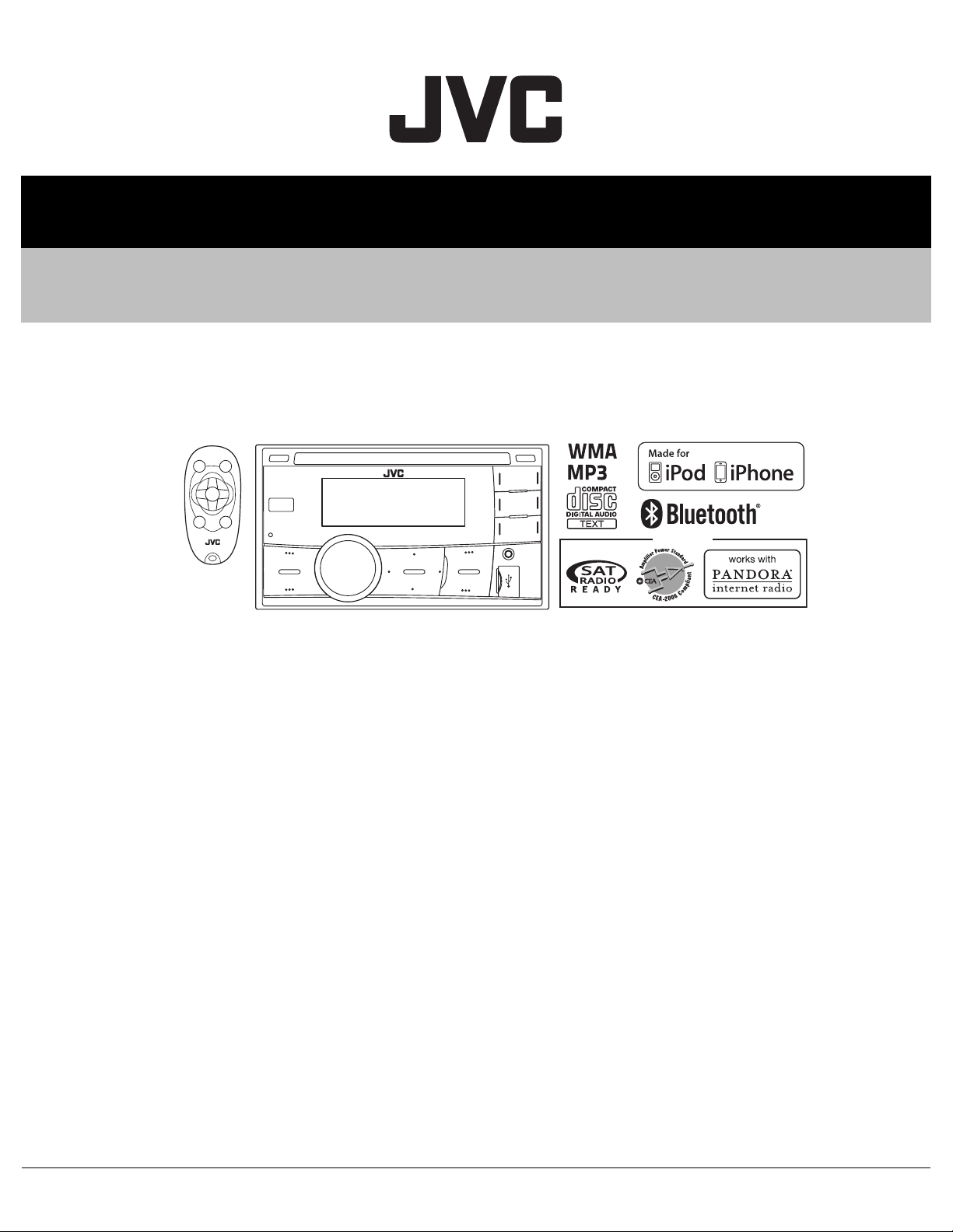
CD RECEIVER
MA520<Rev.001>20121SERVICE MANUAL
KW-R900BTJ, KW-R900BTU
COPYRIGHT © 2012 JVC KENWOOD Corporation
Lead free solder used in the board (material : Sn-Ag-Cu, melting point : 219 Centigrade)
Lead free solder used in the board (material : Sn-Cu, melting point : 230 Centigrade)
For us
COPYRIGHT © 2012 JVC KENWOOD Corporation
No.MA520<Rev.001>
2012/1
Page 2

SPECIFICATION
For US
AUDIO AMPLIFIER SECTION
Power Output 20 W RMS x 4 Channels at 4 Ω and ≤ 1% THD+N
Load Impedance 4 Ω (4 Ω to 8 Ω allowance)
Frequency Response 40 Hz to 20 000 Hz
Signal-to-Noise Ratio 80 dBA (reference: 1 W into 4Ω)
Line-Out or Subwoofer-Out Level/Impedance 5 V/20 kΩ load (full scale)
Output Impedance ≤ 600Ω
TUNER SECTION
FM Frequency Range 200 kHz step: 87.9 MHz to 107.9 MHz
50 kHz step: 87.5 MHz to 108.0 MHz
Usable Sensitivity 9.3 dBf (0.8 µV/75Ω)
50 dB Quieting Sensitivity 16.3 dBf (1.8 µV/75Ω)
Alternate Channel Selectivity (400 kHz)
Frequency Response 40 Hz to 15 000 Hz
Stereo Separation 40 dB
AM Frequency Range 10 kHz step: 530 kHz to 1 700 kHz
Sensitivity/Selectivity 20 µV/40 dB
CD PLAYER SECTION
Signal Detection System Non-contact optical pickup (semiconductor laser)
Number of Channels 2 channels (stereo)
Frequency Response 5 Hz to 20 000 Hz
Signal-to-Noise Ratio 102 dB
Wow and Flutter Less than measurable limit
USB SECTION
USB Standard USB 1.1, USB 2.0
Data Transfer Rate (Full Speed) Max. 12 Mbps
Compatible Device Mass storage class
Compatible File System FAT 32/16/12
Playable Audio Format MP3/WMA/WAV
Maximum Supply Current DC 5 V 1 A
BLUETOOTH SECTION
Version Bluetooth 2.1 certified (+EDR)
Power Class Class 2 Radio
Service Area 10 m (10.9 yd)
Profile HFP 1.5, OPP 1.1, A2DP 1.2, AVRCP 1.3, PBAP 1.0
GENERAL
Power Requirement (Operating Voltage) DC 14.4 V (11 V to 16 V allowance)
Grounding System Negative ground
Allowable Operating Temperature 0°C to +40°C (32°F to 104°F)
Dimensions (W × H × D)
(approx)
Mass 1.8 kg (4 lbs) (excluding accessories)
Installation Size 182 mm × 111 mm × 160 mm (7-3/16” × 4-3/8” × 6-5/16”)
Panel Size 188 mm × 117 mm × 18 mm (7-7/16” × 4-5/8” × 3/4”)
65 dB
9 kHz step: 531 kHz to 1 611 kHz
• Subject to change without notice.
• If a kit is necessary for your car, consult your telephone directory for the nearest car audio speciality shop.
(No.MA520<Rev.001>)2/16
Page 3
SPECIFICATION
For ASIA
AUDIO AMPLIFIER SECTION
Maximum Power Output 50 W per channel
Continuous Power Output (RMS) 20 W per channel into 4Ω, 40 Hz to 20 000 Hz at less than 1% total harmonic distortion.
Load Impedance 4 Ω (4 Ω to 8 Ω allowance)
Frequency Response 40 Hz to 20 000 Hz
Signal-to-Noise Ratio 80 dB
Line-Out or Subwoofer-Out Level/Impedance 5 V/20 kΩ load (full scale)
Output Impedance ≤ 600Ω
TUNER SECTION
FM Frequency Range 87.5 MHz to 108.0 MHz
Usable Sensitivity 9.3 dBf (0.8 µV/75Ω)
50 dB Quieting Sensitivity 16.3 dBf (1.8 µV/75Ω)
Alternate Channel Selectivity
(400 kHz)
Frequency Response 40 Hz to 15 000 Hz
Stereo Separation 40 dB
AM Frequency Range 531 kHz to 1 611 kHz
Sensitivity/Selectivity 20 µV/40 dB
CD PLAYER SECTION
Signal Detection System Non-contact optical pickup (semiconductor laser)
Number of Channels 2 channels (stereo)
Frequency Response 5 Hz to 20 000 Hz
Signal-to-Noise Ratio 102 dB
Wow and Flutter Less than measurable limit
USB SECTION
USB Standard USB 1.1, USB 2.0
Data Transfer Rate (Full Speed) Max. 12 Mbps
Compatible Device Mass storage class
Compatible File System FAT 32/16/12
Playable Audio Format MP3/WMA/WAV
Maximum Supply Current DC 5 V 1 A
BLUETOOTH SECTION
Version Bluetooth 2.1 certified (+EDR)
Power Class Class 2 Radio
Service Area 10 m
Profile HFP 1.5, OPP 1.1, A2DP 1.2, AVRCP 1.3, PBAP 1.0
GENERAL
Power Requirement (Operating Voltage) DC 14.4 V (11 V to 16 V allowance)
Grounding System Negative ground
Allowable Operating Temperature 0°C to +40°C
Dimensions
(W × H × D)
Mass 1.5 kg (excluding accessories)
Installation Size approx. 178 mm × 100 mm × 156 mm
Panel Size approx. 184 mm × 112 mm × 22 mm
65 dB
• Subject to change without notice.
(No.MA520<Rev.001>)3/16
Page 4
SECTION 1
PRECAUTION
1.1 Safety Precautions
(1) This design of this product contains special hardware and
many circuits and components specially for safety purposes. For continued protection, no changes should be made
to the original design unless authorized in writing by the
manufacturer. Replacement parts must be identical to
those used in the original circuits. Services should be performed by qualified personnel only.
(2) Alterations of the design or circuitry of the product should
not be made. Any design alterations of the product should
not be made. Any design alterations or additions will void
the manufacturers warranty and will further relieve the
manufacture of responsibility for personal injury or property
damage resulting therefrom.
(3) Many electrical and mechanical parts in the products have
special safety-related characteristics. These characteristics are often not evident from visual inspection nor can the
protection afforded by them necessarily be obtained by using replacement components rated for higher voltage, wattage, etc. Replacement parts which have these special
safety characteristics are identified in the Parts List of Service Manual. Electrical components having such features
are identified by shading on the schematics and by ( ) on
the Parts List in the Service Manual. The use of a substitute
replacement which does not have the same safety characteristics as the recommended replacement parts shown in
the Parts List of Service Manual may create shock, fire, or
other hazards.
(4) The leads in the products are routed and dressed with ties,
clamps, tubings, barriers and the like to be separated from
live parts, high temperature parts, moving parts and/or
sharp edges for the prevention of electric shock and fire
hazard. When service is required, the original lead routing
and dress should be observed, and it should be confirmed
that they have been returned to normal, after reassembling.
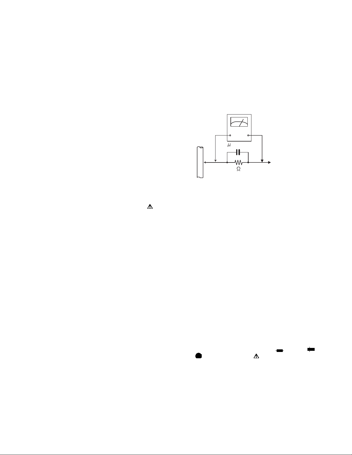
(5) Leakage shock hazard testing
After reassembling the product, always perform an isolation check on the exposed metal parts of the product (antenna terminals, knobs, metal cabinet, screw heads,
headphone jack, control shafts, etc.) to be sure the product
is safe to operate without danger of electrical shock.Do not
use a line isolation transformer during this check.
• Plug the AC line cord directly into the AC outlet. Using a
"Leakage Current Tester", measure the leakage current
from each exposed metal parts of the cabinet, particularly any exposed metal part having a return path to the
chassis, to a known good earth ground. Any leakage current must not exceed 0.5mA AC (r.m.s.).
• Alternate check method
Plug the AC line cord directly into the AC outlet. Use an
AC voltmeter having, 1,000Ω per volt or more sensitivity
in the following manner. Connect a 1,500Ω 10W resistor
paralleled by a 0.15µF AC-type capacitor between an exposed metal part and a known good earth ground.
Measure the AC voltage across the resistor with the AC
voltmeter.
Move the resistor connection to each exposed metal
part, particularly any exposed metal part having a return
path to the chassis, and measure the AC voltage across
the resistor. Now, reverse the plug in the AC outlet and
repeat each measurement. Voltage measured any must
not exceed 0.75 V AC (r.m.s.). This corresponds to 0.5
mA AC (r.m.s.).
AC VOLTMETER
(Having 1000
ohms/volts,
or more sensitivity)
0.15 F AC TYPE
Place this
probe on
1500 10W
Good earth ground
1.2 Warning
(1) This equipment has been designed and manufactured to
meet international safety standards.
(2) It is the legal responsibility of the repairer to ensure that
these safety standards are maintained.
(3) Repairs must be made in accordance with the relevant
safety standards.
(4) It is essential that safety critical components are replaced
by approved parts.
(5) If mains voltage selector is provided, check setting for local
voltage.
1.3 Caution
Burrs formed during molding may be left over on some parts
of the chassis.
Therefore, pay attention to such burrs in the case of preforming repair of this system.
1.4 Critical parts for safety
In regard with component parts appearing on the silk-screen
printed side (parts side) of the PWB diagrams, the parts that are
printed over with black such as the resistor ( ), diode ( )
and ICP ( ) or identified by the " " mark nearby are critical
for safety. When replacing them, be sure to use the parts of the
same type and rating as specified by the manufacturer.
(This regulation dose not Except the J and C version)
each exposed
metal part.
(No.MA520<Rev.001>)4/16
Page 5
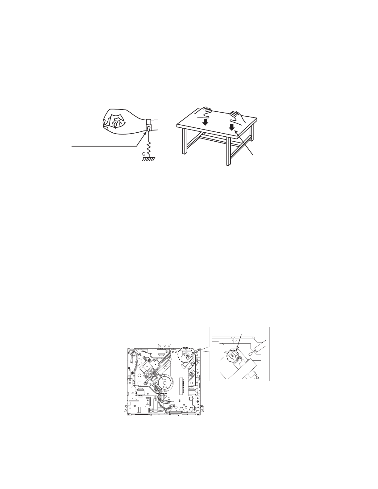
1.5 Preventing static electricity
Electrostatic discharge (ESD), which occurs when static electricity stored in the body, fabric, etc. is discharged, can destroy the laser
diode in the traverse unit (optical pickup). Take care to prevent this when performing repairs.
1.5.1 Grounding to prevent damage by static electricity
Static electricity in the work area can destroy the optical pickup (laser diode) in devices such as laser products.
Be careful to use proper grounding in the area where repairs are being performed.
(1) Ground the workbench
Ground the workbench by laying conductive material (such as a conductive sheet) or an iron plate over it before placing the
traverse unit (optical pickup) on it.
(2) Ground yourself
Use an anti-static wrist strap to release any static electricity built up in your body.
(caption)
Anti-static wrist strap
1M
Conductive material
(conductive sheet) or iron palate
(3) Handling the optical pickup
• In order to maintain quality during transport and before installation, both sides of the laser diode on the replacement optical
pickup are shorted. After replacement, return the shorted parts to their original condition.
(Refer to the text.)
• Do not use a tester to check the condition of the laser diode in the optical pickup. The tester's internal power source can easily
destroy the laser diode.
1.6 Handling the traverse unit (optical pickup)
(1) Do not subject the traverse unit (optical pickup) to strong shocks, as it is a sensitive, complex unit.
(2) Cut off the shorted part of the flexible cable using nippers, etc. after replacing the optical pickup. For specific details, refer to the
replacement procedure in the text. Remove the anti-static pin when replacing the traverse unit. Be careful not to take too long a
time when attaching it to the connector.
(3) Handle the flexible cable carefully as it may break when subjected to strong force.
(4) I t is not possible to adjust the semi-fixed resistor that adjusts the laser power. Do not turn it.
1.7 Attention when traverse unit is decomposed
*Please refer to "Disassembly method" in the text for the pickup unit.
• Apply solder to the short land sections before the card wire is disconnected from the connector on the servo board. (If the card wire
is disconnected without applying solder, the pickup may be destroyed by static electricity.)
• In the assembly, be sure to remove solder from the short land sections after connecting the card wire.
SOLDER
(No.MA520<Rev.001>)5/16
Page 6
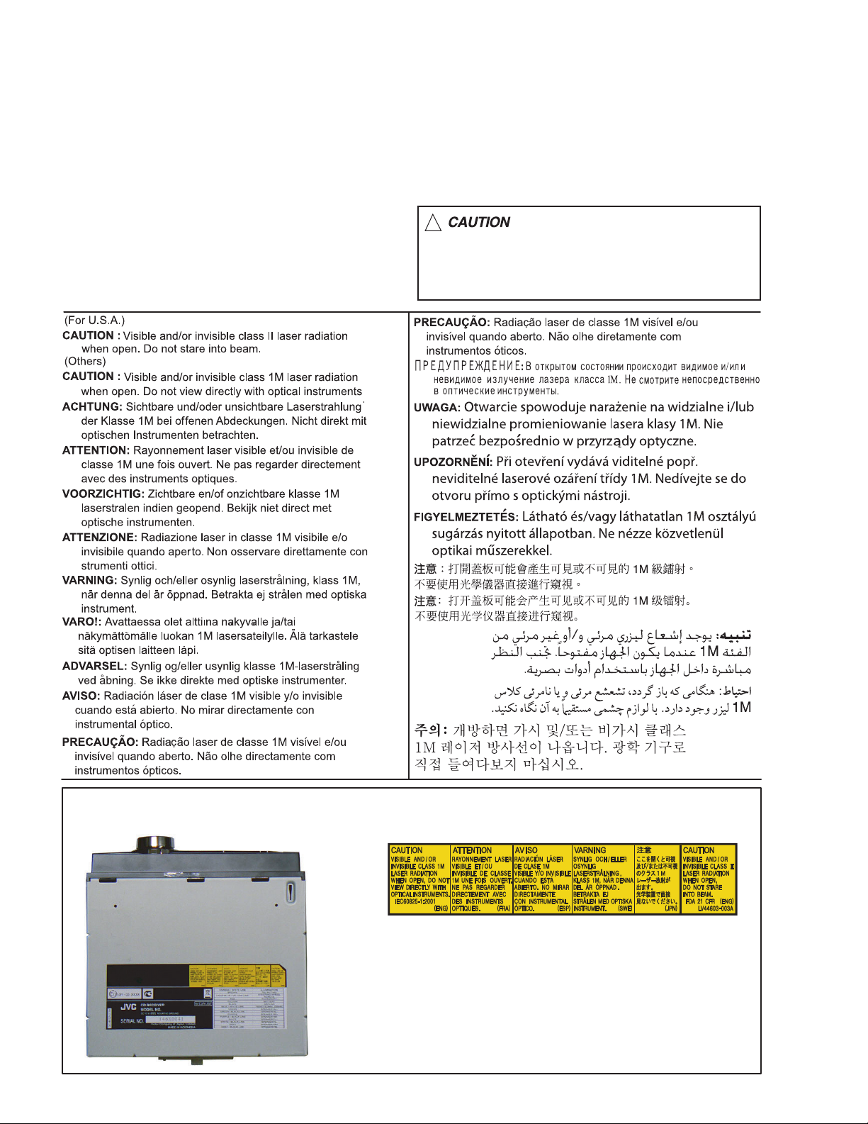
1.8 Important for laser products
1.CLASS 1 LASER PRODUCT
2.CAUTION :
(For U.S.A.) Visible and/or invisible class II laser radiation
when open. Do not stare into beam.
(Others) Visible and/or invisible class 1M laser radiation
when open. Do not view directly with optical instruments.
3.CAUTION : Visible and/or invisible laser radiation when
open and inter lock failed or defeated. Avoid direct
exposure to beam.
4.CAUTION : This laser product uses visible and/or invisible
laser radiation and is equipped with safety switches which
prevent emission of radiation when the drawer is open and
the safety interlocks have failed or are defeated. It is
dangerous to defeat the safety switches.
5.CAUTION : If safety switches malfunction, the laser is able
to function.
6.CAUTION : Use of controls, adjustments or performance of
procedures other than those specified here in may result in
hazardous radiation exposure.
!
Please use enough caution not to
see the beam directly or touch it
in case of an adjustment or operation
check.
REPRODUCTION AND POSITION OF LABELS and PRINT
WARNING LABEL and PRINT
(No.MA520<Rev.001>)6/16
Page 7
SECTION 2
SPECIFIC SERVICE INSTRUCTIONS
This service manual does not describe SPECIFIC SERVICE INSTRUCTIONS.
SECTION 3
DISASSEMBLY
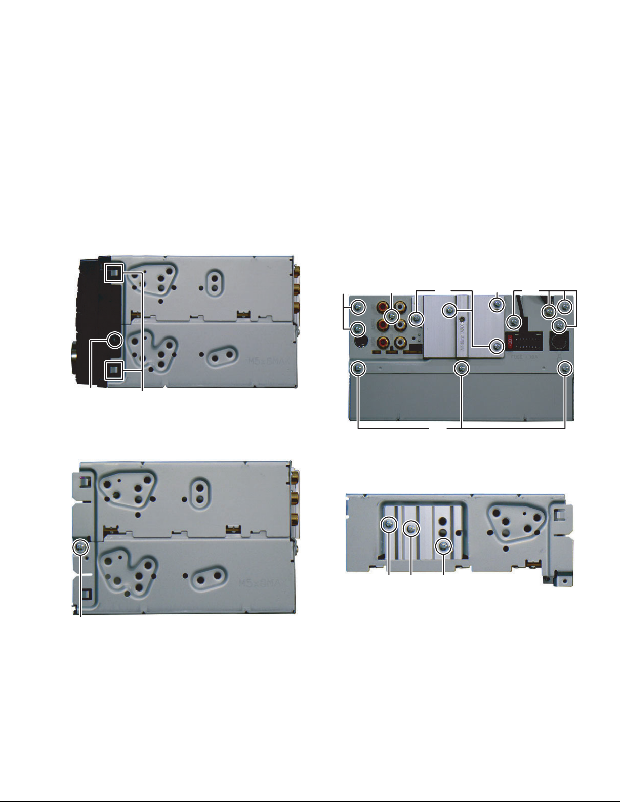
3.1 Main body (Used model: KW-R900BTJ)
3.1.1 Removing the Front panel (See Fig.1)
(1) Remove the 2 screws A attaching the both side of the Front
panel.
(2) Disengage 4 hooks a engaged both side of the Front panel.
(2) Remove the 3 screws C attaching the Bottom chassis.
(See Fig.3)
(3) Remove the 3 screws D and 1 screw E attaching the Heat
sink. (See Fig.3)
(4) Remove the 6 screws F and 1 screw G attaching the Rear
bracket. (See Fig.3)
hook
A
3.1.2 Removing the Bottom chassis (See Fig.2, 3)
(1) Remove the 2 screws B attaching the both side of the Bot-
tom chassis. (See Fig.2)
a
Fig.1
F
G
D F
E
C
Fig.3
3.1.3 Removing the Electric unit (See Fig.4, 5, 6)
(1) Remove the 2 screws H and one screw J attaching the
Side plate. (See Fig.4)
B
HHJ
Fig.4
Fig.2
(No.MA520<Rev.001>)7/16
Page 8
(2) Remove the 3 screws K attaching the Electric unit. (See
Fig.5)
K
K
3.1.5 Removing the Switch unit (See Fig.8)
(1) Remove the Volume knob.
(2) Disconnect the connector wire connected to connector
of the Switch unit.
CN602
(3) Remove the 13 screws M attaching the Switch unit.
CN602
Fig.5
(3) Disconnect B-B connector CN502 of the Electric unit con-
nected the CD mechanism and Electric unit. (See Fig.6)
CN502
Fig.6
3.1.4 Removing the CD mechanism (See Fig.7)
(1) Remove the 3 screws L attaching the CD mechanism.
M
M
M
Fig.8
L
L
Fig.7
(No.MA520<Rev.001>)8/16
Page 9
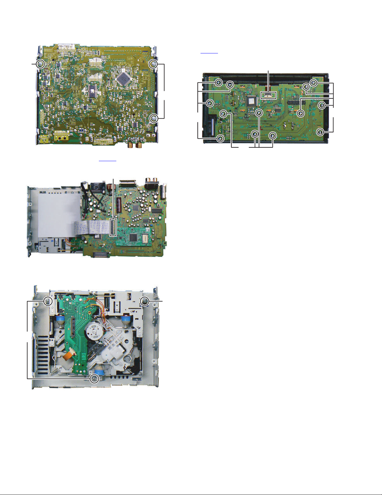
3.2 CD mechanism assembly section
3.2.1 Removing the Mecha control board
(1) Solder the short land on the pickup. (See Fig. 1)
SOLDER
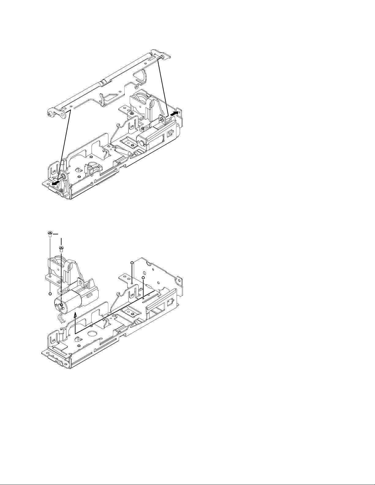
3.2.2 Removing the Traverse mechanism (See Fig.4, 5)
(1) Remove the 5 springs from the traverse mechanism. (See
Fig.4)
Fig.1
(2) Remove the 8 wires from the Mecha control board. (See
Fig.2)
BLACK
RED
WHITE
YELLOW
ORANGE
ORANGE
WHITE
YELLOW
Fig.2
(3) Disconnect the flexible wire from the pickup connected to
the connector CN102
on the Mecha control board. (See
Fig.3)
(4) Remove the 2 screws A attaching the Mecha control board.
(See Fig.3)
Fig.4
(2) Remove the 3 screws B attaching the bottom frame as-
sembly. (See Fig.5)
(3) Remove the 3 dumpers from the bottom frame assembly.
(See Fig.5)
B
B
Fig.5
3.2.3 Removing the Pickup (See Fig.6, 7)
(1) Remove the 2 screws C attaching the feed bracket assem-
bly. (See Fig.6)
CC
Fig.3
A
CN102
Fig.6
(No.MA520<Rev.001>)9/16
Page 10
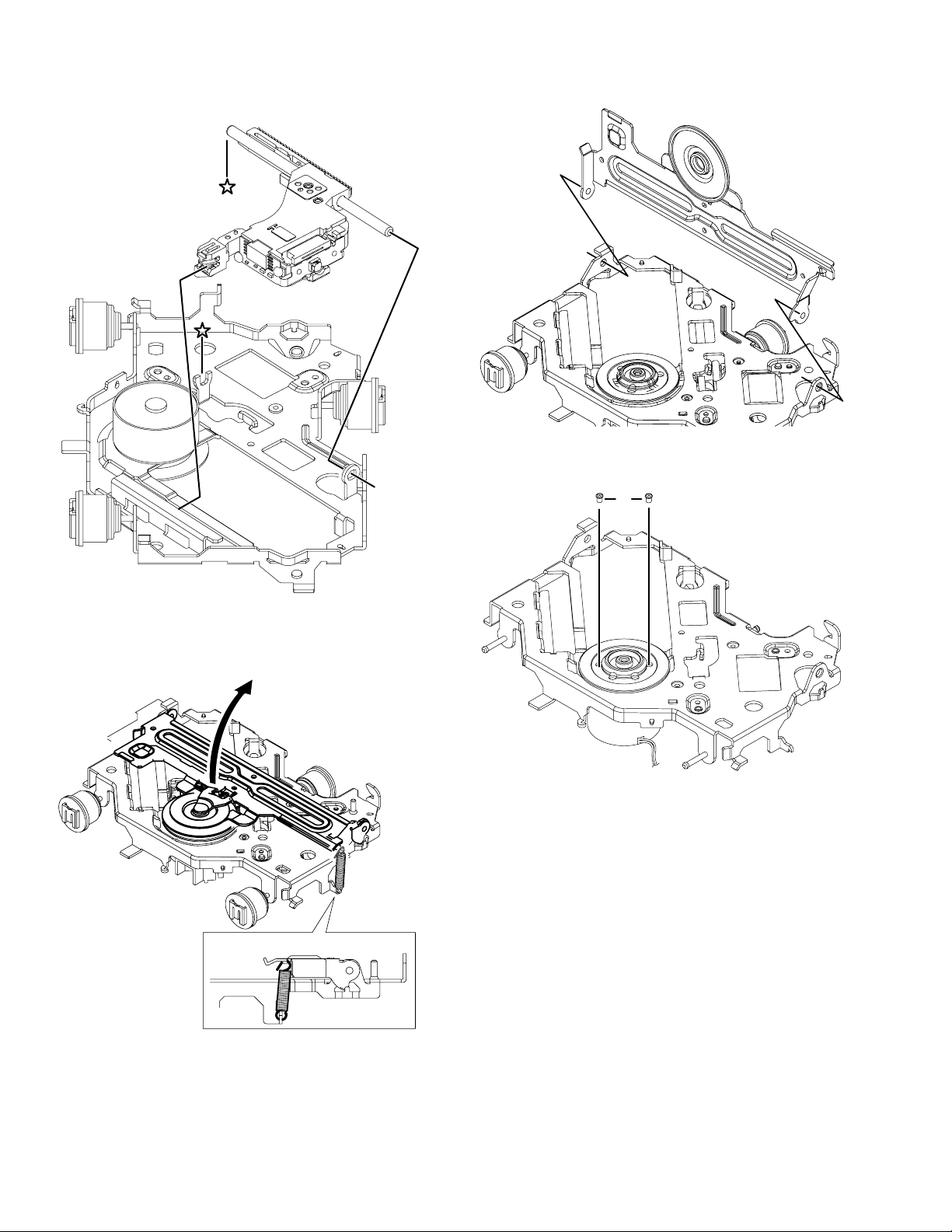
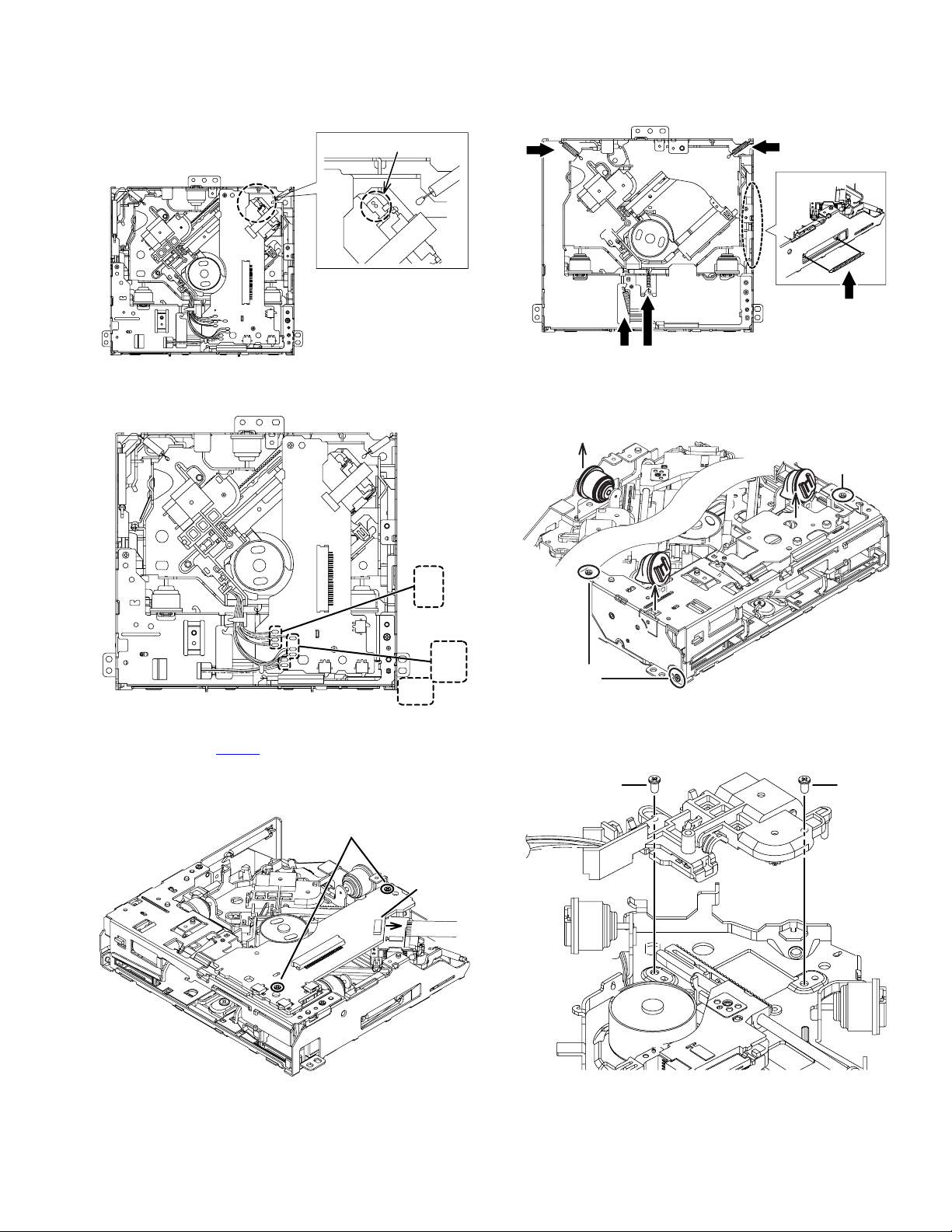
(2) Remove the shaft from the TM base. (See Fig.7)
(3) Disengage the hook a on the pickup from the TM base.
(See Fig.7)
shaft
(2) Remove the HC CL. base from the holes on the TM base.
(See Fig.9)
Fig.9
(3) Remove the 2 screws D attaching the spindle motor. (See
Fig.10)
D
Fig.7
3.2.4 Removing the Spindle motor (See Fig.8. 9)
(1) Remove the HC CL. Spring from the HC CL. base and the
TM base, and then lift up the HC CL. base. (See Fig.8)
HC CL. spring
[ SIDE VIEW ]
Fig.8
Fig.10
(No.MA520<Rev.001>)10/16
Page 11
3.2.5 Removing the Loading motor
(1) Remove the roller arm assembly from the bottom frame as-
sembly. (See Fig.11)
Fig.11
(2) Remove the 2 screws E attaching the loading motor as-
sembly, and then remove the loading motor assembly in
the direction of the arrow. (See Fig.12)
E
Fig.12
(No.MA520<Rev.001>)11/16
Page 12
SECTION 4
ADJUSTMENT
4.1 General Mode Functions
4.1.1 Micon Software / Firmware Version Checking Mode
Refer to “Service Mode” .
4.1.2 Service Mode
Refer to “Service Mode” .
4.1.3 Production Test Mode
Key to enter:
(1) In any Source
(2) In "Power On" condition, press and hold [MENU] + [POW-
ER] for 2s
(3) "PRODUCTION TEST" to be displayed in the display.
(4) Power off and On the unit to return to Normal mode.
Default setting value under Production Mode:
Item Setting
Volume 0 to 44(max)
Beep OFF
Demo OFF
SUB.W LEVEL SUB.W 04
SUB.W LPF MID 85Hz
EQ FLAT
* Only in "Power On" condition will be able to enter the Production Mode. Setting Value cannot be store under Production
Mode.
4.1.4 Volume 44
Key to enter:
(1) In any Source
(2) In "Power On" condition, press and hold [MENU] + [POW-
ER] for 2s → to enter Production Mode.
(3) Press and hold [BACK] + [UP] 3s → to enter Vol 44 mode
(4) LCD display shall display the following information after en-
tering this mode.
4.1.5 Bluetooth Test Mode
Key to enter:
(1) In any Source
(2) Press and hold [BACK] + [POWER] 3s
(3) Press [VOL] Key to select the display item
(4) Select "Mic Test" to test the Quality of the mic (Clear and
no noise).
TEST MODE
MIC TEST
IN PROGRESS
FINISHED
(5) Once "FINISHED", power off and On the unit to return to
Normal mode.
4.1.6 Bluetooth Connectivity Check Mode
* BT Connectivity Check Mode is for user checking BT connectivity.
Key to enter:
(1) Only In Bluetooth mode with the attached USB Bluetooth
Adapter
(2) Press and hold [Phone]+ Press [VOL] 3s → to perform BT
connectivity check mode
4.1.7 User Entry Mode
Key to enter:
(1) Only applicable for J&U series in Tuner Source
(2) Press and hold [DISP] + Press [VOL] 3s
(3) LCD display shall display the following information after en-
tering this mode.
VOLUME 44
Details:The display will shown "VOLUME 44" for 2s. After
2s,it will return back to the initial source.
(5) Power off and On the unit to return to Normal mode.
* Only applicable under Production Mode.
(No.MA520<Rev.001>)12/16
Details:Rename Tuner Station. It can be alphabets/numbers/symbols up to maximum 11 charaters
(4) To rename the Tuner Station, turn [Vol] left or right to select
alphabets/number/symbol
(5) Press [] key for next character.
(6) Press [Vol] to enter/confirm the name of the station.
(7) Press [BACK] to exit the mode.
Page 13
4.2 Service Mode
Force Eject mode
Long Press [Eject]
1DIN: No display on screen as panel will be flipped down.
2DIN: Normal pattern + Eject
Service mode
Key to enter:
(1) In any Source
(2) Press and hold [MENU] + [DOWN] for 3s
(3) Mode Select: [VOL] turn
Service Mode
Mecha Display
Data Clear
VOL press
BACK press
VOL press
BACK press
VOL press VOL press
BACK
press
Version
MAIN**** Panel V***
HD V***** R**-**
MINI V****USB V****
CD ###
Initialize All
VOL turn
Name Clear
VOL turn
CD Error Clear
VOL turn
USB Error Clear
VOL turn
CH Error Clear
VOL turn
Init Bluetooth
Panel micon Rom Correction
Shows Telechips Mini firmware version.
Where ### = HC1, HC2 mecha mount status display
HC1 = HC1 mecha, HC2 = HC2 mecha, *** = can not detect.
This display should be shown in every source with or
without disc inside mecha.
Initialize
After the clearing is a normal pattern
VOL press
Name Clrar
After the clearing is a normal pattern
VOL press
CD Error Clear
After the clearing is a normal pattern
VOL press
USB Error Clear
After the clearing is a normal pattern
VOL press
CH Error Clear
After the clearing is a normal pattern
VOL press
Init Bluetooth
After the clearing is a normal pattern
(No.MA520<Rev.001>)13/16
Page 14
CD Service Mode
BT Memorize Mode
HD Service Mode
* HD model only
VOL press
BACK press
VOL press
BACK press
VOL press
BACK
press
Sequence and description of Labels:-
FG0:- Focus gain automatic adjustment value in normal-speed mode (for setting use)
FEXP0:- Focus gain automatic adjustment value in normal-speed mode (for setting use)
FBAL:- Focus balance adjustment value
FRR:- Focus low-band feedback coefficient
TG0:- Tracking gain automatic adjustment value in normal-speed mode(for setting use)
TEXP0:- Tracking gain automatic adjustment value in normal-speed mode(for setting use)
TBAL:- Tracking balance adjustment value
TRR:- Tracking low-band feedback coefficient
FC:- Focus phase compensation coefficient
FR:- Focus low-band compensation coefficient
TC:- Tracking phase compensation coefficiennt
TR:- Tracking low-band compensation coefficient
FC2:- Focus phase compensation coefficient at vibration
FR2:- Focus low-band compensation coefficient at vibration
TC2:- Tracking phase compensation coefficient at vibration
TR2:- Tracking low-band compensation coefficient at vibration
FG2:- Focus gain coefficient mantissa part at vibration (for setting use)
FEXP2:- Focus gain coefficient exponent part at vibration (for setting use)
TG2:- Tracking gain coefficient mantissa part at vibration (for setting use)
TEXP2:- Tracking gain coefficient exponent part at vibration (for setting use)
TRVG0:- Traverse gain setting
OFSAC:- Ac offset adjustment value
OFSBD:- BD offset adjustment value
OFSE:- W offset adjustment value
OFSF:- F offset adjustment value
OFTD:- OFTduty measurement result
FMAX:- FE signal maximum value (8-bit 2's compliment)
FMIN:- FE signal minimum value (8-bit 2's compliment)
TMAX:- TE signal maximum value (8-bit 2's compliment)
TMIN:- TE signal minimum vlaue (8-bit 2's compliment)
FE_Gain:- Final digital gain setting
TE_IAGain:- TE initial analog gain setting
TE_AGain:- TE analog gain
TE_DGain:- TE digital gain
FE_AGain:-FE analog gain
Corresponding Address (HEX) : 00 ~ 6F
In Progress
*USB device should be connected bofore starting this function.
*Front USB is prioritized if USB devices are connected in both front and rear.
* All key is invalid expect 'Power' key.
SM
IDM
MP
ADJ
***
V***
***
***
Complete or Error Please power off
ROM Correcti on Mode
DCOK
or
DC Error
VOL press
BACK press
VOL press VOL press
BACK press BACK press
VOL turn
IFBW
IF
QI
SNR
BCNT
AGAIN
SPROC
VOL press
BACK press
DC1 OK
DC2 0
No DC error condition
DC1 Error
DC2 x
x:- number of time DC2 is detected
******
VOL turn
ROM CORRECTION
Version
* * * NON : when no ROM correction is done
VXX : when ROM correction is done
*
**
**
*
**
**
***
VOL press
BACK press
Clear DC1 Error?
VOL press: DC1 OK
Clear DC2 Error?
VOL press: DC2 x
(No.MA520<Rev.001>)14/16
Page 15
4.3 DC Offset error description
A
4.3.1 DC Offset detection circuit design
•Purpose:
To prevent breakdown, burning and emitting smoke from customer's car speaker when occur DC offset between speaker
output "+" and "-".
• Target:
Detect DC offset, then stop the Power Amp operation and shift
to specified condition.
4.3.2 Possible causes of DC offset at speaker output lines
(1) Mis-connection for Speaker output for example touch to car
body or battery line.
(2) Current leak of coupling capacitor for Power IC input.
(3) Current leak of Ac-GND capacitor for Power IC Ac-GND.
(4) Capacitor shorted of above parts due to foreign object.
C-tc
E-Vol
Win_TC
Win_In
DC Error
C-in
C-in
R3
C-in
C-in
C-ac2C-ac1
Sw5V
R2
R1
C3
R4
Audio Pwr Amp
In 1
In 2
In 3
In 4
AcGnd
Offset Detect
Out
Micon
ADC In
4.3.3 Type of checking
4.3.3.1 To detect DC Offset Error
• Mis-connection
- Short any one speaker out line to GND or Vcc
• Capacitor leak
- Parallel 330kΩ to either any one of coupling cap or Ac-GND
cap (to simulate current leakage of capacitor)
- Shorted either any one of coupling cap or Ac-GND cap.
4.3.3.2 To avoid mis-judge music as DC offset error
• Low frequency signal (17Hz or 20Hz) is more prone to cause
mis-detection.
- Play 17Hz (or 20Hz) signal and make sure micon will not de-
tect and judge this as happen DC offset error.
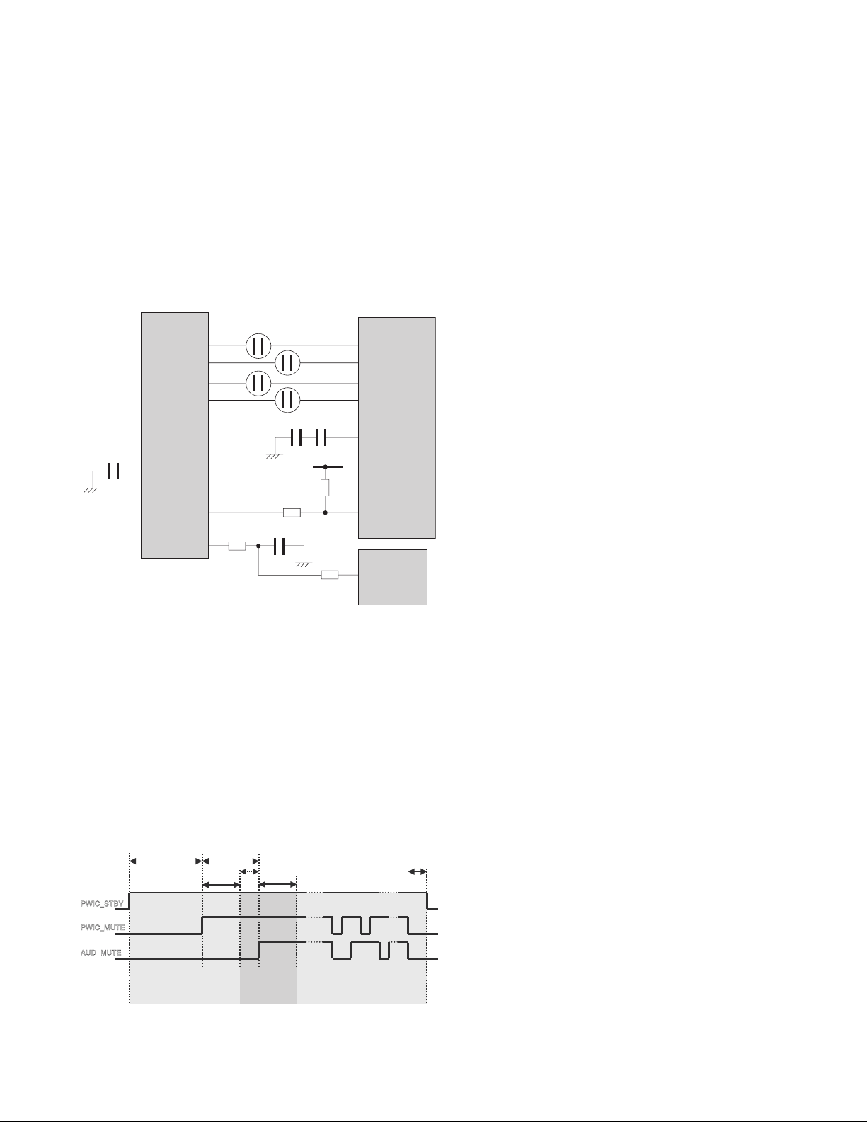
4.3.4 Detection Timing chart
50ms
or more
PWIC_STBY
PWIC_MUTE
2.0sec or more
1.5sec or more
0.8sec
0.7sec or more
1.0sec
4.3.5 Manipulate after detect DC Offset
• If detected error 10 consecutive times, and 10th error occurred
in "Mis-connect detection period", judge as "Mis-connect".
• If detected error 10 consecutive times, and 10th error occurred
in "Capacitor leak detection period", judge as "Capacitor leak ".
• If detected error 10 consecutive times, and 10th error occurred
in "Other detection period" and detected another 10 errors consecutively, then judge as "Other".
• If judge as "Mis-connect".
- turn off speaker output.
- display "MIS WIRING" → "CHK WIRING" → "THEN RESET"
→ "UNIT".
- key access disable except button of Eject, Reset and service
mode
- record error in EEPROM "DC1 ERR"
- Set is able to be recovered by Reset button.
• If judge as "Capacitor leak ".
- turn off speaker output.
- display "WIRING" → "CHK WIRING" → "THEN RESET" →
"UNIT".
- key access disable except button of Eject, Reset and service
mode
- record error in EEPROM "DC2 #" (# means counter number)
- Set can be recovered by pressing the Reset button before
the capacitor leak error counter reach "DC2 4".
After that, only clear the counter back to "0" can recover the
set.
• If judge as "Other" (manipulation same as mis-connect)
4.3.6 How to clear the DC offset error recorded in EEPROM
Refer to”Service Mode”.
SECTION 5
TROUBLESHOOTING
This service manual does not describe
TROUBLESHOOTING.
UD_MUTE
Missconnect
detection period
Capacitor leak
detection period
Other (miss detection etc.)
detection period
(No.MA520<Rev.001>)15/16
Page 16

JVC KENWOOD Corporation
Car Electronics Business Group 2967-3, Ishikawa-machi, Hachioji-shi, Tokyo, 192-8525, Japan
(No.MA520<Rev.001>)
Printed in Japan
VSE
Page 17

SCHEMATIC DIAGRAMS
18
CD RECEIVER
KW-R900BTJ KW-R900BTU
(No.MA520<Rev.001>)1/
Page 18

■ PRECAUTIONS ON SCHEMATIC DIAGRAMS
z Due to the improvement in performance, some part numbers shown in the circuit diagrams
may not agree with those indicated in the Parts List.
z The parts numbers, values and rated voltage etc. in the Schematic Diagrams are for
reference only.
z Since the circuit diagrams are standard ones, the circuits and circuit constants may be
subject to change for improvement without any notice.
■ PRECAUTIONS ON PARTS LIST
z
The parts identified by the symbol are critical for safety. Whenever replacing these parts, be sure to
use specified ones to secure the safety.
z
The parts not indicated in this Parts List and those which are filled with lines --- in the Parts No.
columns will not be supplied.
z
P.W. BOARD Ass'y will not be supplied, but those which are filled with the Parts No. in the Parts No.
columns will be supplied.
z
When ordering chips, screws etc., place bulk orders (unit of tens) whenever possible to improve
shipping efficiency.
z
There are cases where the actual implemented parts in the sets and the service parts are different.
When ordering parts, make sure to refer to the Parts List.
■
PRECAUTIONS ON SERVICE
Certain parts of the power circuits and the GNDs differ according to the models. Care must be
taken for the following points as the differences are indicated separately in the LIVE GND ( ) and
the ISOLATED (NEUTRAL) GND ( ).
1. Do not touch the LIVE GND, or do not touch the LIVE GND and the ISOLATED (NEUTRAL)
GND at the same time. It may cause an electric shock.
Before pulling out the chassis or other parts, make sure to pull out the power cord from the
wall outlet first.
2. Do not short circuit between the LIVE GND and ISOLATED (NEUTRAL) GND, or never
measure the LIVE GND and ISOLATED (NEUTRAL) GND at the same time using measuring
instruments (oscilloscope, etc.). It may blow fuses or damage other parts.
■ DEVIATION TOLERANCE RANGE
DEVIATION TOLERANCE RANGE
F G J K M N R H Z P
± 1% ± 2% ± 5% ±10% ±20% ±30%
+30%
-10%
+50%
-10%
+80%
-20%
+100%
-0%
18
(No.MA520<Rev.001>)2/
Page 19

IC941
LDO 5V
(1A)
IC932
LDO 5V
(1A)
IC931
DC/DC
CONVERTOR
IC921
3.3V LDO
REGULATOR
IC902
3.3V LDO
IC901
REGULATOR
JVC
IC801
BUS
IC771
EEPROM
MICON
IC701
REMOCON
IC681
LCD DRIVE
IC661
IC601
CONVERTOR
D/A
IC601
CONTROL
RGB
CD
L.P.F.
IC581
CD
DSP
IC541
BTL
DRIVER
IC501
1.8V
REGULATOR
IC491
IC481
iPOd IC
IC471
MCLK SW
USB/CD
IC442
SDRAM
FLASH ROM
IC441
IC402
EEPROM
IC401
TELECHIPS
USB DSP
AMP
IC301
POWER
IC201
AUDIO DSP
ELECTRICAL
VOLUME
IC161
IC90
MIC AMP
TUNER IC
IC1
RESET
SWITCH
LINE OUT REAR
J321
LINE OUT
LINE OUT FRONT
SUBWOOFER
FRONT LEFT(+)
FRONT LEFT(-)
FRONT RIGHT(+)
FRONT RIGHT(-)
REAR LEFT(+)
REAR LEFT(-)
REAR & FRONT
SUBWOOFER
MUTING
CIRCUIT
RST
MUTE
MICON PS2
REAR L
REAR R
FRONT R
FRONT L
SUBWOOFER
VDD5V
DC-OFFSET
CLLIPDET
VDD3.3V
14.4V MEM
SWREG
EN 0
6.2V
GND
EN0
CD-L
CD-R
6.2V
EN1
GND
FLG0, FLG1
P.IC MUTE
& MUTING
TRANSISTORS
CN901
DETECT
DIMMER INPUT
TU.L
TU.R
REAR RIGHT(-)
AUTO ANT, AMP REMOTE
STEERING REMOTE
TU/RDSCL
TU/RDSDA
EEPROM-DI
EEPROM-DO
EEPROM-CLK
To SPK,
BATTERY, GND
ANT JACK
MI
CN472
UH1+
UH1-
GND
USB5V R
CN90
(REAR)
To USB Cable
PS2
MUTE
MICON
CDON
PS1
CTRL1
CTRL2
ILM
POWER
VOL DA
VOLCK
MUTEA
MUTE0
MUTE1
MUTE2
EN0
EN1
BEEP
SW1
BUSINT
BUSSCK
/BUSI/O
BUSSI
BUSSO
ACIN2R
ACIN2L
ACOUTR
ACOUTL
ACIN0R
ACIN0L
ACIN1R
DISPPDN
VOLCK
VOLDA
RESET
ACIN1L
For J version
J-DATA
J-CLK
ADIN0
CH.L
CH.R
J801
To JBUS Connector
For J version
SW5V
PS2 BATT
REAR RIGHT(+)
DC ERR
EACH BLOCK
ELECTRIC UNIT
NRST
LRCK
MSW
BCK
SRDATA
BLKCK
3.3V
TRST
MUTE CTL
UART TX
UART RX
CDMCLK
ADIN0
UH0+/UH0-
UH1+UH1-
AOUT L/R
LOAD
MCLK
MDATA
SD_SEL
SW1
SW2
PSW
SW3
SPINDLE+
FEED+
FEED-
TRACKING+
TRACKING-
SPINDLE-
3.3V
CN442&CN441&CN444
CN442&CN441&CN444
SDA/SCL
AOUT L/R
ADIN0
CDON
TRST/MUTE CTL/UART TX/UART RX
USBH1D+/USBH1D-
USBH0D+/USBH0D-
SW1/SW2/SW3/PSW
LOAD/MSW
USB UNIT
BLOCK DIAGRAM
1.8V
DAO1
BCLK1
/DACMS
LRCLK1
DACMC
DACMD
MCLK
CLK SW/MCLK1
EPSDA/EPSCL
CDMCLK
FEED+
CD PLAYER UNIT
XA0-21
XD0-15
MLD/BLKCK/NRST/MDATA/MCLK/STAT/BCK/LRCK/SRDATA
FOCUS-
FOCUS+
VF1.VF2
VT1.VT2
MD.LD
3.3V
DISPRST
CIRCUIT
DISP RESET
GND
USB5V
CN502
CN101
SW1
SW2
SW3
PSW
UH0+
UH0-
KEYDATA
DISPCLK
DISPDATA
DISPCE
REMOCON
CN701
CN601
TRACKING+
FOCUS+
TRACKING-
FOCUS-
MOTOR
POSITION
SET SWITCH
PICK UP
MOTOR
SPINDLE
PSW
SPINDLE+
SPINDLE-
SW1
SW2
SW3
VF1/VF2
VT1/VT2
LD/MD
REMOCON
DISPCE
R,G.B
SDA,SCL
ALL LEDs
SW1,SW2,SW3
GND
USB5V
D-
D+
VOL2
EN601
VOL1
ILL 10V
KEYDATA
DISPRST
DISPCLK
CN603
ROTARY
KEY0
KEY1
D0-D7
VDD
S661 TO
LCDWR/RD
THERMAL
LCDCL/CS/RST
SWITCH UNIT
KEY
S677
ENCODER
J601
AUX IN
FRONT USB
USB JACK
CN602
LCD
DISPDATA
FEED-
LOAD&FEED
STAT
SW5V
AOUT L/R
created date:2012-01-17No.MA520
18
(No.MA520<Rev.001>)3/
Page 20

CONDITION
---FM MODE. ( )CD MODE.AM MODE.
3.3V
3.3V
3.3V
3.3V
3.3V
3.3V
3.3V
3.2V
0V
2.4V
2.4V
2.4V
0.0V
8.3v4v4v
4v
4v4v4v
4v
4v
8.3v
0v
3.4v
3.3v
3.3v
3.3v
3.3v
3.3v
3.3v
8.3V
2.8V
4.2V
2.8V
7.6V
0.7V
3.3V
0.8V
0V
5.2V
4.9V
0V
5.2V
5.2V
3.3V
10.0V
14.4V
1.6V
4.4V
1.0V
1.2V
0V
5.2V
1.6V
3.3V
9.9V
14.4V
1.0V
1.2V
0V
5.2V
0V
3.3V
3.3V
0.1V
3.3V
3.3V
4.2V
0.2V
0V
0V
0V
0.6V
3.0V
0V
0V
4.8V
0V
0V
0V
0V
3.3V
3.3V
(1/8W)
0v
(1/10W)
SYNCVCFB
GND
EN
LX
BST
IN
SYNCVCFB
GND
EN
LX
BST
IN
NCEN
GNDNC
FBNC
VCC OUT
RESET
DISPRST
USB_5V
USB_GND
USB_GND
D+
D-
AUX_L
REF1B
VSS4
AUDIO DSP
1.8v
DZF
PDN
VSS3
SDA
SCL
2.4V
CLKO
2.4V
DVDD
2.4V
2.4V
2.4V
3.3V
0.0V
4.8v
4.8v
4.8v
3.3V
2.1v
0.0V
2.1v
2.4V
0.0v
0.0V
0.0V
AOUT2L
AOUT3L
AOUT3R
AVDD
VREFH
VSS1
TSTI
VCOM
AINL
AINR
AOUT1R
AOUT1L
AOUT2R
BICK
LRCK
SDT01
SDT02
SDT03
XTI
XTO
VSS2
3.3v
3.3v
NC
NC
TU-SDA
TU-SCL
7 6 532
1
LEARNING2
LEARNING1
22K
22K
22K
22K
RT1P141C-X
RT1N141C-X
10K
10K
10K
10K
RT1P241C-X
RT1N241C-X
4.5v
3.3v
3.3v
3.3v
3.3v
3.3v
3.3v
3.3v
0v
8.3v
0v
3.3v
3.3v
3.3v
3.3v
3.3v
3.3v
3.3v
3.3v
7.0V
7.0V
7.1V
4.6V
4.9V
4.9V
4.9V0V4.9V
2.2V
14.3V
14.4V
1.6V
8.4V
0V
0V
1.25V
1.25V
9.9V
AUX_G
NC
BUZZER
**
ONLY
NOT USED/USEDUSED/NOT USED
L10 / R9
10K/5.1KNOT USED/10K
CLIPDET
RE.USB5V
FR.USB5V
QAM1331-001 QAM1332-001
0V
0V0V0V
0V0V
5V DSP REG
(1/10W)
(1/10W)
NC
PITSWL
OUTSWR
VDDLD
GNDLD
OUTLR
OUTLF
OUTRF
OUTRR
WINTC2
WINTC1
DCERR
WININ
MUTE2
MUTE1
MUTE0
MUTEA
SE1L
SE1R
SE0R
SE0L
QD1RDCSEL
NC
QD1L
QD1G
QD0R
QD0G
QD0L
CREF
GNDA
VCC
SDA
SCL
SE2R
SE2L
ACOUTL
ACOUTR
ACIN0L
ACIN0R
ACIN1L
ACIN1R
ACIN2L
ACIN2R
NC
MUTE2
MUTE1
MUTE0
C204-C207,C214-C217: QERF1EM-475Z-E
USED
KW-R900BTU
USED
5V
ILM.10V
ILM.ADJ
CTRL2
9V
SW5V
VDD5V
ACC.IN
DISPCE
DISPCLK
DISPDATA
KEYDATA
REMOCON
10V
C335-C338: NCB21CK-474X-A
IS COMBINED. BUT POP NOISE MIGHT OCCUR.
CURRENT CONDITION: SUB-MUTE AND NORMAL MUTE
ADD D781,Q781
IF SUB-MUTE NEEDS TO BE SEPARATED FROM
NORMAL MUTE, WE NEED TO:
REMOVE R786 (3 PAIR)/ REMOVE R785 (2 PAIR)
MUTING
IN
EN
SW3.3V
*
*
TELMUTE
OE REMOTE
FRONT RIGHT(+)
FRONT RIGHT(-)
FRONT LEFT(-)
FRONT LEFT(+)
REAR LEFT(+)
REAR LEFT(-)
REAR RIGHT(-)
REAR RIGHT(+)
5V
*
CIRCT
RST
MICON
DISP.
ONLY
SERIES
KD-R820
FOR
MUTE
SUBMUTE
PW.IC MUTE
SW5V
VDD3.3
RESET
PS2
MUTING CIRCUIT
BATT DETECT PS2
CD8V
9V-ADJ
MEM-IN
CTRL1
GND
ACC5V
ANTOUT
EXT
0V
0V
0V
0V
0V
0V
0V
0V
0V
0V
0V
0V
0V
3.2V
3.2V
3.2V
0V
0V
0V
0V
3.1V
2.6V
3.1V
3.3V
0V
0V
3.2V
3.3V
3.3V
0V
0V
3.4V
0V
0V
0V
(1/10W)
*
FLAG1
FLAG0
NC
NC
NC
NC
NC
NC
NCOPEN
NC
RxM
NCNCNCNCNCNCNC
MUTEA
NC
DSPPDN
D711-D713:
3.3V
0V
4.9V 4.9V
AGND
( )
VOUT
VIN
GND
CTRL
*
*
*
NOT USED
JVC BUS CIRCUIT, R759, R762, R763,R764, R765, C163, C173
NOT USED
AUTO ANTENNA CIRCUIT
KW-R900BTJ
GND
9V-TCC
UH0-
USB3.3
GND
USB5V
MUTE.CTL
TRST
USBRX
USBTX
UH0+
*
MEMORY
ACC
REMOTE
AUTO ANTENNA
GND
ILLUMINATION
EACH
USE 1/10W
R5 & R8
KW-R900BTJ
USED FOR
MAIN PWB:GEB10326A
CIRCUIT
SUBWOOFER
FOR U VERSION ONLY
SUBWOOFER 5V AMP
E.VOLUME
REMOTE
STEERING
UNLESS OTHERWISE SPECIFIED.
NOTES
2.
1. VOLTAGES ARE DC-MEASURED WITH A DIGITAL VOLT METER WITHOUT INPUT SIGNAL
ALL RESISTANCE VALUES ARE IN OHM.
ALL E.CAPACITORS ARE SHOWN IN THE FORM OF CAPACITANCE(uF)/RATED VOLTAGE(V)
3.
ALL CAPACITORS ARE 50V OR 25V CERAMIC CAPACITOR.
ALL CAPACITANCE VALUES ARE IN uF(P=pF)
ALL RESISTORS ARE 1/16W 5% METAL GLAZE RESISTOR.
COMPONENTS IN ( ) INDICATE NOT USE.
4.2V
0.7V
7.0V
-CL
ROUT
0V
0V
+RIN
8.3V
-CR
-RIN
2.8V
LOUT
CRPR
VCCR
2.8V
+LIN
VCCL
-LIN
7.6V
+CL
CRPL
+CR
GNDL
7.0V
GNDR
VCC
DSPRST
KEYDATA
4.1v
-
-
+
+
GND
4.1V
0v
4.2v
4.2v
4.2v
CIRCUIT
MIC PREAMP
VCC
8.3v
4.2v
EEPROM-DI NC
DCERR
OFFSET
TAB
POWER CORD ASS'Y
0V
3.1V
0V
0V
0V
4.9V
4.9V
0V
0V
0V
0V
0V
0V
3.2V
Vdd
GND
2.2V
5.0V
2.0V
1.8V
4.2V
2.9V
8.3V
8.3V
0V
2.2V
4.5V
5.6V
0V
8.3V
6.8V
3.9V
3.2V
3.2V
0V
5.9V
5.9V
3.9V
3.7V
0.4V
3.8V
3.3V
3.1V
3.3V
3.3V
3.3V
3.3V0V3.3V
1.6V
3.3V
3.3V
3.8V
0V
8.3V
3.1V
3.3V
0V
0V
0V
3.1V
3.3V
0V
0V
3.1V
0V
3.3V
1.1V
1.5V
0V
0V
2.5V
1.1V
1.4V
3.3V
3.3V
3.3V
3.2V
0V(3.3V)
3.3V
3.2V
3.1V
3.3V
3.3V
0V
0V
4.5V
3.2V
0V
3.2V
0V
0V
0V
0V
0V
0V
0V
0V
0V
0V
0V
0V
1.4V
0V
0V
AMSELOUT2
AMSELOUT1
AMIFAGC1
AMSELIN2
AMSELIN1
PLL2
PLLREF
PLL1
VCO
GNDRF
VCC
VREG
VREF
SDA
SCL
DGND
XTAL
TEST
RSSI
MPXOUT
MPXIN
AMIFAGC2
AGND
ROUT
LOUT
AMRFAGC
VCC
GNDRF
FMRFIN1
FMRFIN2
AMRFIN
AMRFDEC
4.4V
1.6V
1.6V
3.0V
6.6V
6.6V
3.7V
3.8V
3.8V
3.2V
3.2V
7.1V
7.2V
7.6V
2.8V
2.8V
8.3V
2.8V
0V
0V
0V
3.3V
0V
0V
3.3V
0V
2.8V
0V
0V
0V
0V
14.4V
0V
7.1V
7.0V
4.5V
7.0V
7.1V
0V
7.0V
6.9V
6.9V
0V
6.9V
6.9V
7.0V
7.6V
0V0.9V
7.0V
2.8V
2.8V
4.2V
2.8V
2.8V
7.1V
0.9V
FB4
0V
4.9V
7.1V
CIN1
0V
3.3V
3.3V
3.3V
3.3V
RLOUT
FB2
RLIN
V+
RRIN
RROUT
CIN2
L/O 5V AMP
GND
0V
COUT2
FROUT
MUTING
(1/8W)
A0
A1
A2
WPIN
MUTING
GND
VOL-CLK
VOL-DA
CDON
PS1
PS2
STEERING REMOTE
ANT CONT
PIC-STBY
FB3
FRIN
14.4V
ANTENNA
USBRX
USBTX
BUS-INT
EEPROM-D0
POWER CORD
REGULATOR
LINE OUTPUT
REMOCON
S-GND
USB RESET
LINE OUT
CLIPDET
R747 (L)/R748 (H)MICON STAGE SETTING =
CPU
*
* REMARKS
(1/10W)
(1/10W)
0V
0V
USBMUTE CONT
JVC BUS
POWER AMP.
TUNER
FM/AM
REF
(1/10W)
A-GND
BUS-I/0
OUTFL-
EEPROM
GND
FLIN
INFL
OUTFL+
OUTRL+
OUTRL-
MUTE
INRL
SVR
GND
OUTFR-
GND
OUTFR+
INFR
INRR
OUTRR-
GND
VCC3/4
GND
TAB
OUTRR+
VCC1/2
AC-GND
STBY
FB1
MEMORY.IN
BUS-SO
BUS-SI
Vdd
SCL
BUS-SCK
FLOUT
COUT1
DISPCE
DIMMER INPUT
/BUS-I/O
CHANGER CONTROL
STAGE1
SDA
DETACH
EJECT
SWREG
SUBMUTE
NC
GND
NC
NC
AUTO
GND
VDD
NC
DIMMER IN
AVREF0
REGC
EEPROM-CLK
DISPCK
DISPDATA
EVDDO
FLMDOX1EVSSO
VSSX2VDD
XT1
XT2
RESET
DEBUG-DA
DEBUG-CLK
NC
NC
VDD
T.M
SW1
(TXM)
SUBWOOFER OUTPUT
&
SW3.3V
*
ILM
POWER
USB_5V
DSPPDN
HC2-DET
MIC
EN1
EN0
SWREG
SWREG
MMRY
CH.L
CH.R
/BUS-I/O
J-CLK
J-DATA
SWREG
REMOCON
VDD3.3V
RST
DISPCE
DISPCLK
DISPDATA
KEYDATA
RESET
RESET
RESET
UH0+
UH0-
CD.R
CD.L
TUSCL
TUSDA
MUTE
PIC-STBY
POWER
OUTRL
OUTFL
OUTRR
OUTFR
LEARN2
LEARN1
EN1
EN0
UH0+
CLIPDET
CLIPDET
PS2
LEARN1
LEARN2
AUX_L
AUX_G
AUX_R
CH.L
CH.R
E-SL
E-SR
EV-RL
EV-FL
EV-FR
EV-RR
EVFR
EVRLEVRL
EVFL
EVRR
EVRR
VOLDA
VOLCK
ACCO
STEERING
MUTE
BUZZER
PS2
PIC-STBY
RESET
OFFSET
BUZZER
AUX_L
AUX_G
AUX_R
AUX_R
CD8V
E-SL
E-SR
DCERR
DSPPDN
MUTEA
MUTE0
MUTE1
MUTE2
KEYDATA
EVFR
EVRR
EVRL
EVFL
EV-FR
EV-RR
EV-RL
EV-FL
VOLCK
VOLDA
VOLCK
VOLDA
DCERR
OFFSET
MUTE2
MUTE1
MUTE0
MUTEA
STEERING
HC2-DET
CTRL
OUTFL
OUTRL
OUTFR
OUTRR
OE-REMOTE
ACC5V
OUTRL
DSPRST
ANTENA
SBMUTE
SBMUTE
BUSSI
BUSSO
BUS-I/O
EEPROMDI
OUTFR
FRO
FLO
OUTFL
BUSSCK
CD.R
CD.L
REMO
FL+
SW1
SW1
OUTRR
RLO
RRO
TUSCL
MUTE.CTL
DSPRST
TUSDA
EEPROMDI
DISPCLK
RL-
RL+
FL-
FL+
FR+
FR-
RR+
RR-
REMOCON
BUSINT
PS1
MUTE.CTL
TRST
UH0-
FR+
RR+
FR-
PS2
USBRX
USBTX
ANT
RR-
FL-
RL-
TRST
BUS-I/O
BUSSO
BUSSI
RL+
BUSSCK
/BUS-I/O
BUSINT
DISPDATA
DISPCE
FRO
FLO
RRO
USBTX
USBRX
RLO
MEMORY
9V-TCC
SW1
CD8V
GND
MIC
GND
USB3.3V
MUTE.CTL
TRST
URX
UTX
USB5V
HC2-DET
CD.R
UH0-
CD.L
UH0+
sure to use the specified one.
When replacing those parts make
Parts are safety assurance parts.!
!
!
!
!
!
!
!
!
!
43
2 1
NAX1133-001X
X201
1 2 3
X701
NAX0647-001X
X11
QAX0952-001Z
X702
QAX0401-001
VDD
RESET
VSS
FLMDO
TOOL0
DEBUGCLK
MIC+
MIC-
TM
RXM
TXM
R939
NI
R4
4.7K
R6
220
R365
33k
R7
220
R761
3.9K
R947
1K
R941
91k
R903 5.6k
R943
10k
R801
3.9K
R806
100K
R807
100
R809
6.8K
R901
10k
R812
3.9K
R804
100
R805
47K
R977
47k
R799
47k
R727
2.2k
R722
2.2k
R730
15k
R759
1K
R726
22K
R976
68k
R8
47
R172
NI
R162
NI
R161
0
R171
0
R763
4.7k
R766
10K
R756
10K
R762
0
R975
47k
R925
10k
R924
1.5k
R921
4.7k
R755
22K
R707
1k
R949
270
R764
4.7k
R740
3.9K
R706
1K
R754
22K
R352
330
R301
1K
R945
10k
R946
10k
R302
1K
R316
10k
R317
4.7K
R312
1K
R311
1K
R932
24k
R935
47K
R933
10k
R342
330
R739
3.9K
R341 4.7k
R5
47
R931
91k
R785
0
R309
10
R304
4.7K
R725
39K
R98
10k
R102
0
R101
8.2k
R351 4.7k
NI
R91
R717
47k
R103
0
R97
8.2K
R95
120k
R723
2.2k
R96
33K
R99
120k
R1040
R94
1.2k
R92
8.2k
R93
1.2k
R100
10k
R216
4.7K
R215
4.7K
R724
2.2k
NI
R798
R797
2.2K
NI
R796
R353
180
R728
2.2k
R704 NI
R90
10k
R794
0
R793
10k
R792
10k
R711
4.7k
R720
47k
R814
0
R773
NI
R783
10k
R343
180
R758
10K
R738
47K
R175
100
R165
100
R786
0
R265
330
R276
4.7K
R267
180
R757
1K
R275
330
R274
22k
NI
R374
R273
NI
R769
100k
R195
470
R770
470k
R1
680K
R271
22k
R272
33k
R768
12K
R2
680K
R14
3.3k
R324 22k
R314
1K
R313
820
NI
R373
R310
4.7k
R163
0
NI
R233
NI
R232
NI
R231
R278
33k
R15
3.3k
R306
10k
R307
4.7K
R268
33k
R743
10k
R716
150
R7350R734
0
R185
470
R721
180k
R1980R197
0
R187
0
R188
0
R277
180
R948
220k
R191
0
R192
0
R936
220k
R182
0
R266
4.7K
R181
0
R264
22k
R752
47K
R263
NI
R713
47k
R714
47k
R334 22k
R213
820
R203
820
R212
820
R202
820
R211
820
R201
820
R907 6.8k
R902 6.8k
R344 22k
R944
1k
R934
1k
R942
24k
R354 22k
R705
15k
R745
47K
R746
47k
R749
47K
R803
6.8K
R205
2.2
R702
10M
R715
47k
R206
1.5K
R782
330
R703
0
R772
270
R204
100
R214
100
NI
R371
NI
R372
R732
0
R851
4.7K
R733
0
R708
0
R709
0
R710
470
R332
330
R322
330
R771
270
R922
0
R923
0
R718 NI
R331
4.7k
R321
4.7k
NI
R16
NI
R17
R904
270k
R981 3.3k
R791
10k
R790
100k
NI
R3
R737
1.2K
R9
0
R333
180
R744
47K
R751
47K
R742
47K
NI
R305
R323
180
R747
R811
100K
R972
10k
R971
10k
R767
1K
R712
100
R973 20k
R974
47k
R261
22k
R808
47K
R882
47K
R905
4.7k
R906
27k
R765
1K
R361
33k
R810
100K
R362
22k
R366
22k
R386
22k
R385
33k
R781
47K
R881
27K
R731
10k
R262
33k
R382
22k
R381
33k
R719
47k
R729
22k
R701
47k
R760
22k
R748
Q881
DRC2114E-X
DRC2124E-X
Q783
DRC2114E-X
Q301
NI
Q781
Q782
DRA2114E-X
DRA2124E-X
Q784
Q971
2SC1623A/5-6/-X
NI
Q231
Q970
2SC1623A/5-6/-X
2SC1623A/5-6/-X
Q702
Q701
2SA812A/5-6/-X
L701
4.7
NI
L7
L702
4.7
L901
QQR1883-001
L2
1.8
QQL92AK-220Z
L931
L1
0.47
L201
47
QQL92AK-220Z
L941
L6
560
L3
0.27
L162
10
L9
0.47
L5
560
L703
47
L8
4.7
NQLH25M-4R7X
K941
NQR0269-026X
L10
NQL79GM-101X
L902
NQLH25M-4R7X
K931
K171
0
NQL553J-27NX
L161
K162
0
K172
0
15 14
13
12 11 10 9
8 7 6 5
4 3 2 1
QNZ0095-001
J801
100
99
98
97
96
95
94
93
92
91
90
89
88
87
86
85
84
83
82
81
80
79
78
77
76
75 74 73 72 71 70 69 68 67 66 65 64 63 62 61 60 59 58 57 56 55 54 53 52 51
50
49
48
47
46
45
44
43
42
41
40
39
38
37
36
35
34
33
32
31
30
29
28
27
26
25242322212019181716151413121110987654321
UPD78F1168GS
IC701
4443424140393837363534
3332313029282726252423
2221201918171615141312
11 10 9 8 7 6 5 4 3 2 1
TDA7716N
IC161
1 2 3 4 5 6 7 8 9 10 11 12 13 14 15 16
17181920212223242526272829303132
IC1
TEF6614TV1S4-X
1 2 3 4 5 6 7 8 9 10 11 12 13 14 15
161718192021222324252627282930
AK7600VF-X
IC201
123456789101112131415161718192021222324252627
TDA7851A
IC301
12345678910
11 12 13 14 15 16 17 18 19 20
IC361
NJM2792V-X
12345678
9 10 11 12 13 14 15 16
IC271
NJM2160BV-X
151413121110987654321
LV5680P
IC901
1234567
8 9 10 11 12 13 14
IC801
74AHCT126PW-X
9
8765
4 3 2 1
BD9673EFJ-X
IC941
9
8 7 6 5
4321
BD00GA3WEFJ-X
IC921
9
8765
4 3 2 1
BD9673EFJ-X
IC931
1234
5 6 7 8
IC771
BR24T02FJ-W-X
1 2 3 4
8 7 6 5
NJM4565E-X
IC90
654
3 2 1
IMX9-W
Q322
654
3 2 1
IMX9-W
Q332
654
3 2 1
IMX9-W
Q261
VIN
5
EN4/OC
3
GND
2
VOUT
1
RT9715EGB-X
IC932
43
2 1
IC902
XC6213B332NG-X
8 7
6 4
321
QQR1872-001
L4
NMFZ018-3R0X-E
F902
FUSE
QMFZ064-100-J1
BAW56-TP-X
D722
D782
BAW56-TP-X
NI
D781
D261
BAW56-TP-X
D331
BAW56-TP-X
D783
BAW56-TP-X
D321
BAW56-TP-X
MC2838-X
D721
NI
D702
D706
NI
D707
NI
D703
NI
RKZ6.2B2KG-X
D711
NI
D231
NAF0029-001X
D3
NI
D201
NI
D709
D714
RKZ6.2B2KG-X
D713
NI
D710
NI
D715
NI
D717
D971
RKZ6.8B2KG-X
D705
NI
D970
RKZ6.8B2KG-X
D704
NI
D712
NI
D708
D719
RKZ6.2B2KG-X
D718
RKZ6.2B2KG-X
D852
MBRX130-TP-X
1N5401-BPC04
D901
D1
NI
RB051L-40-X
D931
RKS801KF-X
D784
D851
MBRX130-TP-X
RB051L-40-X
D941
D2
NI
D982
MBRX130-TP-X
RKS801KF-X
D785
D981
MBRX130-TP-X
C266
10/25
C261
4.7/50
C262
10/25
C276
10/25
C919
NI
C271
4.7/50
C273
100/16
C733
10/25
C917
220/6.3
C907
100/16
C96
22/16
C368
220/10
C369
22/16
C367
220/10
C103
22/16
C381
4.7/50
C216
4.7/25
C206
4.7/25
NI
C952
C361
4.7/50
C26
100/16
C214
4.7/25
C204
4.7/25
QEKJ1CM-107Z-S
C169
100/16
C205
4.7/25
C365
10/25
QEKJ0JM-107Z-S
C209
100/6.3
QEKJ1HM-225Z-S
C210
2.2/50
C385
10/25
QEKJ1CM-106Z-S
C221
10/16
C366
10/25
C386
10/25
QTE1C57-106Z
C224
10/16
C922
100/6.3
NI
C851
C914
NI
NI
C913
C215
4.7/25
QEKJ1CM-476Z-S
C178
47/16
C908
220/10
QEKJ1HM-225Z-S
C170
2.2/50
C910
10/25
QEKJ1HM-225Z
C189
2.2/50
4.7/35
QTE1V67-475Z
C172
C905
47/16
QTE1V67-475Z
C162
4.7/35
QEZ0936-278
C901
C723
330/6.3
QEKJ1HM-225Z
C199
2.2/50
C909
330/6.3
C881
22/16
QEKJ1HM-105Z-S
C161
1/50
C217
4.7/25
C207
4.7/25
1/50
QEKJ1HM-105Z-S
C171
QTE1C57-476Z
C317
47/16
C382
4.7/50
C949
150/6.3
NIC924
C903
47/16
C904
100/16
C362
4.7/50
C316
4.7/50
NI
C27
C387
220/10
C939
150/6.3
C902
2.2/50
QERF1CM-106Z-E
C306
10/16
C263
100/16
QTE1C66-474Z
C312
N
QTE1C66-474ZC301
N
QTE1C66-474ZC302
N
QTE1C66-474ZC311
N
C307
0.01
C308
0.01
C305
82P
C303
56p
C304
56p
C313
56p
C314
56p
C315
1.0
C705
NI
C100
0.027
C101
22p
C94
330p
C104
0.1
C102
0.033
C99
0.027
C97
330p
C739
47p
C741
47p
C731
0.047
C732
0.047
NI
C926
NI
C927
C953
100p
C724
100p
C725
10
C713
0.47
C711
680p
C712
680p
C15
0.1
C34
NI
C35
NI
C173
1
C163
1
C264
0.1
C265
0.0015
C98
0.033
C709
0.1
NI
C786
C105
8p
NI
C91
NI
C90
C730
820p
NI
C734
C707
NI
C168
1000p
C25
0.01
C13
1
C14
0.22
C6
27p
C4
0.22
C334
NI
C332
NI
C333
NI
C331
NI
C916
3300p
NI
C912
C982
0.1
C7
470p
NI
C780
0.47
C335
0.47
C336
0.47
C337
0.47
C338
NCB21AK-105X-A
1
C318
C179
1000p
C223
0.1
C227
12p
C226
12p
C225
0.1
C222
1000p
C220
1000p
C208
1000p
C218
1000p
C211
1800p
C201
1800p
C202
1800p
C212
1800p
C203
1800p
C213
1800p
C181
470p
C182
470p
C192
470p
C191
470p
C185
3300p
C735
1
NI
C238
1000p
C239
C736
1
C738
1
C275
0.0015
C195
3300p
C274
0.1
C267NIC277
NI
C340
NI
C343NIC339NIC342
NI
C737
1
NI
C743
C784
1
C785
2.2
C30
56p
C991
NI
C993
NI
C32
27p
NI
C236
C95
1
C933
0.1
10
C934
C938
0.01
10
C931
C932
10
NI
C936
10
C935
C937
6800p
C744
100P
C719
100P
C92
1
C93
1
C706
NI
C742
1000p
C948
0.01
10
C941
C942
10
C947
6800p
C943
0.1
NI
C946
10
C945
10
C944
C951
0.47
C950
1
100p
C237
C928
390p
1000p
C235
C106
100p
C745
NI
C234
4700p
27p
C233
NI
C740
C325
NI
NI
C726
NI
C720
NI
C852
C918
0.01
C715 0.1
C31
NI
C8
2p
C319
0.022
C371
0.1
C370
0.0015
C372
0.0015
C990
27p
C716
1
NI
C28
C701
22P
C10
1
C702
27P
C703 NI
NI
C29
C704 NI
C714
100P
NI
C729
C771
0.047
C310
82P
NI
C321
C968
470p
C966
470p
C967
470p
C965
470p
C964
470p
C324
NI
C920
NI
C5
15p
C911
0.1
C963
470p
C962
470p
C961
470p
C341
NI
C802
C9
5.6p
C3
0.001
C22
12p
C1
0.001
C23
0.1
NI
C981
C721
0.047
C2
7p
C19
0.1
NCJ30JM-106X-A
C925 10
C16
0.01
C718
0.1
C18
0.01
C727
0.047
C12
0.01
C11
0.01
C717
0.047
C906
0.1
C915
0.1
C388
0.1
C17
0.1
C24
0.01
C801
0.047
NI
C782
C722
0.01
C320
0.022
C921
1
C322
NI
NI
C783
C323
NI
QNB0190-001
J1
24
23
22
21
20
19
18
17
16
15
14
13
12
11
10
9
8
7
6
5
4
3
2
1
QGB1004K1-24
CN701
123456789
101112131415161718
CN901
QNZ0607-001
8765432
1
QNN0877-001
J321
3
2
1
NI
CN702
2
1
CN90
QGA2001F1-02
ELECTRIC UNIT-1
To ELECTRIC UNIT-2
CN601
To SWITCH UNIT
BATTERY, GND
To SPK,
To ELECTRIC UNIT-2
created date:2012-01-17No.MA520
18
(No.MA520<Rev.001>)4/
Page 21

CONDITION
---FM MODE. ( )CD MODE.AM MODE.
4.8V
3.3V
3.3V
3.2V
0V
3.4V
( )
1.7V
1.7V
3.0V
3.2V
3.4V
3.3V
3.0V
3.2V
0V
1.7V
3.4V
0V
0V
0V
HOT!
HOT!
1.7V
1.7V
1.3V
4.8V
4.8V
5.4V
7.1V
5-CH BTL DRIVER
0V
6.3V
7.1V
1.7V
1.7V
1.7V
1.7V
1.7V
1.7V
0V
DSP
GND
USB.GND
H: HC2
L: HC1
HC2-DET
CD.L
A.GND
CD.R
SW1
9V-TCC
CD8V
MIC
SW3
GND
NOT USED
1/10W
1/10W
2.4V
3.1V
1.9V
1.7V
1.7V
1.7V
1.6V
1.6V
1.6V
1.7V
0V
0V
3.4V
1.7V
1.7V
1.5V
0V
0V
2.1V
3.3V
0V
3.2V
1.7V
0V
1.5V
0V
3.4V
0.1V
1.7V
1.7V
0.6V
3.4V
3.4V
1.6V
1.7V
0V
3.3V
0V
1.6V
0.1V
0V
0V
0V0V0V
3.3V
0V
3.4V
0V
0V
1.4V
1.4V
1.7V
0.8V
0V
1.7V
1.3V
1.2V
1.1V
1.0V
1.7V
1.6V
1.9V
3.4V
2.4V
0.2V
1.9V
1.9V
1.9V
1.9V
2.0V
2.0V
0V
A.
GND
GND
USB5V
MUTE.CTL
TRST
USBRX
USBTX
UH0+
UH0-
3.3V
4.2V
8.3V
4.2V
0V
4.2V
-
+
4.2V
+
-
GND
Vcc
4.2V
4.2V
USB.GND
BLKCK
PSW
USB.GND
U1-
U1+
USB3.3V
U0-
U0+
USB0.EN
USB1.EN
A_MUTE
RESET
URX
UTX
MIC
DAC_L
DAC_R
A_GND
A9V
GND
USB.GND
CD16M
D_BCLK
D_LRCLK
NRST
D_SDATA
STAT
MLD
MDATA
MCLK
SW2
SW1
REV
B.MUTE
FWD
USBH1
* CSEL: L(R544)-16.9344MHz
SERVO DSP
H(R545)-33.8688MHz
GND
GND
NOTES
ALL E.CAPACITORS ARE SHOWN IN THE FORM OF CAPACITANCE(uF)/RATED VOLTAGE(V)
UNLESS OTHERWISE SPECIFIED.
1. VOLTAGES ARE DC-MEASURED WITH A DIGITAL VOLT METER WITHOUT INPUT SIGNAL
2.
COMPONENTS IN ( ) INDICATE NOT USE.3.
ALL CAPACITANCE VALUES ARE IN uF(P=pF)
ALL RESISTANCE VALUES ARE IN OHM.
ALL CAPACITORS ARE 50V OR 25V CERAMIC CAPACITOR.
ALL RESISTORS ARE 1/16W 5% METAL GLAZE RESISTOR.
MAIN PWB: GEB10326A
SP+
SP-
VREF
CBCLK
CLRCK
SRDATA
MLD
MDATA
MCLK
STAT
LOAD-
LOAD+
FEED+
FEED-
FOCUS-
FOCUS+
TRK-
TRK+
TRP
FOP
TRVP
SPOUT
REV
FWD
VCC
UH1-
UH1+
FOCUS+
FOCUS-
TRK+
TRK-
LD
FEED-
FEED+
SP-
SP+
LOAD+
LOAD-
HC2-DET
MD
VT1
PSW
VT2
SW1
VF2
SW2
SW3
VF1
HC2-DET
PSW
SW1
SW3
SW2
FWD
REV
BLKCK
NRST
STAT
MCLK
SRDATA
MDATA
CBCLK
CLK16M
MLD
CLRCK
VF1
VT1
VT2
VF2
BLKCK
NRST
MD
FOP
TRP
SPOUT
TRVP
CLK16M
UH0+
UH0-
CD.L
CD.R
MIC
MUTE.CTL
USB3.3V
GND
TRST
GND
URX
UTX
USB5V
SW1
GND
HC2-DET
9V-TCC
CD8V
sure to use the specified one.
When replacing those parts make
Parts are safety assurance parts.!
!
123
X521
QAX0714-001Z
EXT0
DQSY
OSCIN
SMON0
SMON1
MONON
SMCK
VREF
ARF
PCMK
TX
EXT3
EXT2
EXT1
FLAG
EXT4
R505
8.2k
R509 8.2k
R524
68k
R522
5.1k
R517
6.8k
NIR543
R521
8.2k
NI
R526
R516 10k
47kR565
R513
15k
R554 1k
R518 8.2k
R508
10k
0R560
R504
8.2k
R540
820
R510
8.2k
0R548
R507 2.2k
R588
27k
R523
33k
R519 47k
R546 22
R550 1k
R503
33k
R506
NI
10R563
R552
220
R553
1M
R601
10
8.2kR559
R520 10
NI
R570
NI
R569
NI
R568
R544 0
R577
33
R576
33
R575
33
R585
8.2k
R551
1k
R587
27k
R594
10k
R593
10k
R591
10k
R511
5.6k
R592
10k
R549 10k
0
R561
R586
8.2k
R583
24k
10R564
R571
33
R572
33
R541 2.7k
R502 6.8k
NI
R479
0R556
R584
24k
R573
33
R478
NI
R574
33
NI
R475NIR476
R477
NI
NIR555
22R547
R512 15k
R545 NI
0
R562
82k
R542
8.2kR558
R501
NI
R514
8.2k
R515
5.6k
0R557
R566
0
2SB1424/R/-WQ501
2SA2188/F/-X
Q540
1
4 3
2
LF472
NQR0682-001X
1.8L521
K581
NQR0022-005X
DQSY 80
(BCLK) GIO2 79
(LRCK) GIO1 78
(SRDATA) GIO0 77
NSRVMONON 76
IOVDD2 75
X1 74
X2 73
DVSS2 72
NRST 71
BLKCK 70
STAT 69
MLD 68
MDATA 67
MCLK 66
TX 65
FLAG 64
TEST 63
NTEST2 62
DVDD2 61
CSEL60EXT059(CD16M) EXT1
58
EXT257EXT356EXT455LSPWM54AVDD153OUTR52NC51AVSS150OUTL49RFVDD248VCOF47PLLFO246PLLFO45PLLF44IREF43DSLF42NC
41
RFVSS2
40
NC39
ARFIN38
ARFFB37
ARFOUT36
ARFDC35
RFIN34
RFOUT
33
RFENV32
CENV
31
RFVDD1
30
LD29
PD
28
A
27
C
26
B25
D
24
F
23
E
22
RFVSS1
21
CTRCRS
20
VREF
19
OSCIN
18
FOP
17
TRP
16
TRVP2
15
TRVP
14
SPOUT
13PC12FG11
DVSS1
10
DVDD1
9
IOVDD1
8NC7NC6NC5
SRVMON14SRVMON0
3
PMCK2SMCK
1
MN6627553PA
IC541
38
GND
37
GND
36
S-GND
35
VCONT
34
MUTE1
33
MUTE234
32
VIN4-
31
VIN4
30
VREF-IN
29
VREF-OUT
28
REG-OUT
27
REG-IN
26
VIN+OP
25
VIN-OP
24
VO-OP
23
VIN3
22
VIN3-
21
VIN2
20
VIN2-
19
VIN2+
18
VIN117VIN1-16VIN1+15VCCS14VCCP113VO1+12VO1-11VO2-10VO2+
9
VO3-8VO3+7VO4-6VO4+5VLO+4VLO-3VCC22REV1FWD
LA6565-XIC501
1234
8765
NJM8801E-X
IC581
VCC
5Y4
GND3IN2NC
1
NI
IC540
NAF0029-001X
D478
NAF0029-001X
D477
GS1J-LTP-X
D501
GS1J-LTP-X
D502
47/6.3C559
47/6.3
C545
47/6.3
C550
47/6.3
C558
C591
NI
QEKJ0JM-476Z-S
C590
47/6.3
QERF1EM-475Z-E
C585
4.7/25
QERF1EM-475Z-E
C586
4.7/25
C511
100/16
C513
47/16
C515
100/6.3
C543
10/25
C541
10/25
C579
10/25
C576
10/25
C571
10/25
C521
82p
4.7C555
C572 NI
0.33
C569
2700p
C549
0.1
C546
0.1C551
0.015C563
C584
820p
C477 22p
0.1C573
C476 NI
C578 0.1
3300pC553
C493 10
0.33
C554
C592
0.1
C581
NI
C560
0.1
C588
150p
C566 0.082
C582
NI
C587
150p
C583
820p
C992
2200p
NI
C548
C478
22p
0.1
C570
C475
NI
C519
470p
C501
2200p
C507
6800p
C562
0.1
C577 0.1
C574 0.1
C520
470p
C506 NI
C509
68p
C518
NI
C516 0.1
0.1
C542
C503
5600p
C502 NI
C561
0.1
0.1C556
C504
NI
C565
1000p
C514 NI
0.15
C547
C508 NI
C568 1000p
0.022C552
C517
1000p
0.1
C544
C539
NI
1000p
C510
C512
0.1
680pC557
C575
0.1
C505
2200p
C540
NI
0.1C564
NIC567
470p
C538
C589
470p
C537
820p
VF1
26
SW3
25
D3.3V
24
SW2
23
VF2
22
SW1
21
VT2
20
PSW
19
VT1
18
VREF
17
MD
16
GND
15
HC2-DET
14
LOAD-
13
LOAD+
12
SP+
11
SP-
10
FEED+
9
FEED-
8
GND
7
LD
6
GND
5
TRK-
4
TRK+
3
FOCUS-
2
FOCUS+
1
CN502
QGF1049F1-26X
181716151413121110
987654321
NI
CN442
181716151413121110
987654321
NI
CN441
5
4
3
2
1
QGA2001C1-05
CN472
2
1
NI
CN444
ELECTRIC UNIT-2
To ELECTRIC UNIT-1
CN444
To USB UNIT
CN442
To USB UNIT
CN441
To USB UNIT
CN101
To CD PLAYER UNIT
created date:2012-01-17No.MA520
18
(No.MA520<Rev.001>)5/
Page 22

( )
0
10V
USB5V
USB_D-
USB_D+
USB5V
0V3.3V
GND VDD
3.3V
OUT
REMOCON
0V
5V
0V
0V
0V
0V
0V
5V
5V 5V
0V
0V
0.1V
0V
0V
0V
0.2V
0V
0V
0V
0V
0V
1
4.7
4.7K
GEB10329A2
USBGND
USBGND
USB
RESET SWITCH
10K
10K
0.047
RKZ3.9B2KG-X
7p
7p
10/16
RKZ3.9B2KG-X
RKZ3.9B2KG-X
RKZ3.9B2KG-X
RKZ3.9B2KG-X
0.0047
0.0047
47K
47K
0.022
0.022
RESET
6
5
21
4
3
NCJ11EK-106X-R
RPT/PHONE
5.6V
10V
5.0V
NCB31CK-105X
RGB DRIVER
AUXL
AUXR
AUXG
REMOCON
DISPRST
DISPCLK
DISPCE
DISPDA
( )
0V
NBE21CM-106X
T3-8
T3-7
T3-6
T3-5
T3-4
T3-3
NCB20JK-475X
3.27V
3.27V
3.28V
3.28V
3.27V
3.27V
1.25V
3.22V
3.18V
3.18V
3.17V
3.17V
3.16V
3.17V
3.21V
3.17V
3.23V
3.28V
0V
3.27V
3.27V
3.28V
0V
3.26V
3.26V
3.28V
1.6V
1.62V
3.26V
3.28V
0V
3.28V
0V
0V0V0V
0V
0V
0V
0V
0V
0V
0V
0V
0V
0V
0V
0V0V0V
3.26V
3.26V
3.28V
3.28V
SWITCH PWB : GEB10329A1
T3-2
LED
0V
0V
0V
0V
3.3V
3.3V
3.3V
3.25V
MICON IC661
FOR PROGRAMMING
3.25V
3.3V
B
A
SELECT
EQ
MENU
PWR/SRC
ENCODER
EJECT
T3-1
COLOR/RND/
KEY MATRIX
DOWN
UP
VCC
D-
D+
GND
BACK/TP
DISP
AUX IN
B-SKIPF-SKIP
NBE20JM-106X
NCB20JK-106X
AUXG
KEY1
KEY0
BLUE
GREEN
LCDDA
LCDCLK
LCDCD
LCDRST
LCDCS
LCDCD
LCDDA
LCDCLK
PTTX
PTCK
D-
D+
KEYDATA
KEYDATA
DISPDATA
DISPCLK
DISPCE
DISPRST
VDD3.3V
10V
RESET
RESET_DISP
RED
VLED
KEY2
KEYIN
AUXR
AUXL
KEY2
KEY0
KEY1
SCL
SDA
VOL2
VOL1
LCDCS
PTRX
E8_BUSY
CNVSS
R
G
B
KEYIN
KEYDATA
DISPDATA
DISPCLK
E8_BUSY
PTCK
PTRX
PTTX
DISPRST
VOL1
VOL2
CNVSS
D+
D-
RGB
LCDRST
DISPCE
SCL
SDA
1
2
3
X661
NAX0613-001X
T2-4
CE
EPM
PTRX
RST
PTCK
CNVSS
E8-BUSY
PTTX
VDD
GND
T2-2
T2-1
T2-3
T1-4
T1-2
T1-1
T1-3
NAD0028-103X
TH601
S691
NSW0246-001X
4
3
2
1
NSW0246-001X
S668
4
3
2
1
NSW0246-001X
S677
4
3
2
1
NSW0246-001X
S661
4
3
2
1
NSW0246-001X
S662
4
3
2
1
NSW0246-001X
S663
4
3
2
1
NSW0246-001X
S664
4
3
2
1
NSW0246-001X
S665
4
3
2
1
NSW0246-001X
S666
4
3
2
1
NSW0246-001X
S667
4
3
2
1
NSW0246-001X
S676
4
3
2
1
NSW0246-001X
S669
4
3
2
1
NSW0246-001X
S670
4
3
2
1
NSW0246-001X
S671
4
3
2
1
NSW0246-001X
S672
4
3
2
1
NSW0246-001X
S673
4
3
2
1
NSW0246-001X
S674
4
3
2
1
NSW0246-001X
S675
5
6
7
8
4
3
2
1
RA663
NI
567
8
432
1
RA662
NI
R650 4.7K
R669 10k
R683
330
R692 4.7K
R668 15k
R645
100
0
B697
R701 1.5K
R702 2.2K
R703 2.2K
R652 680
R691 4.7K
B606
NI
R623
1.2K
R684 4.7K
R698
330
R622
820
R654 1K
R655 1K
R658
47K
R666 10K
R675
330
R693 10K
R681
0
R694 10K
R678
NI
R688
NI
R663
1M
R686
NI
R682
NI
R637
10M
R685
1K
R644
1K
R606 NI
R647
2.2K
R659
NI
R679
10K
R631
820
R635
2.7K
R633
1.2K
R634
1.8K
R632
820
R660 150K
R627
820
R680 10K
R615
1K
R613
1.2K
R614
1.2K
R649
680
R657
47K
R674 47K
R616
1.2K
R617
1.2K
R639
2.2K
R638
2.2K
R628
1.2K
R690 10K
R626
820
R665 330
R656 10K
R602 100
R601 100
R643 NI
R604
1K
R618 330
R646
47K
R662
0
R630
2.7K
R697
470K
R624
1.8K
R621
820
R648
NI
R651 4.7K
R629
1.8K
R689
10K
R653
680
B642
0
R642 47K
R641 47K
R664 10K
R605
0
R661 2.2K
R696 47k
R695 47k
R603 1K
R607 330
R608 330
R609 750
R610 820
R611 820
R612 1.2K
R619 330
R620 750
R667
1K
R671 10K
R699
NI
R687
1K
R670 10k
R625
2.7K
Q601
2SC1623A/5-6/-X
Q603
2SA812A/5-6/-X
Q602
2SA812A/5-6/-X
3
2 1
4
LF691
NQR0682-001X
L661 47u
L603
47u
NQR0007-002X
L690
NQR0022-005X
L604
NQR0007-002X
L677
NQR0007-002X
L687
3 4
12
5
QSW1231-002
EN601
NC100
NC99
RY/BY98
AVCC97
VREF96
NC95
AVSS94
KEY093
KEY192
KEY291
THERMAL90
ANA89
NC88
MEMRST87
D086
D185
D284
D383
D482
D581
D680
D779
P1078
P1177
P1276
P1375P1474P1573P1672P17
71A070A169A268A367A466A565A664A763
VSS
62A861
VCC2
60A959
A1058A1157A1256A1355A1454A1553A1652A17
51
A18 50
A19 49
FLASHCS 48
LCDCS 47
LCKCL 46
LCDDA 45
/CE 44
LCDWR 43
LCDRD 42
NC 41
NC 40
E8_EPM 39
NC 38
NC 37
NC 36
DISPCLK 35
DISPDATA 34
KEYDATA 33
E8_BUSY 32
PTCK 31
PTRX 30
PTTX 29
NC 28
NC 27
NC 26
NC25NC24NC23NC22NC21/OE20LCDRST19KEY_IN18DISPCE17NC16NMI15VCC114XIN13VSS12XOUT11RESET10XCOUT9XCIN8CNVSS7BYTE6VOL15VOL24SCL3SDA2NC
1
R5F3650KDFB
IC661
VSS
1
A0
2
A1
3
A2
4
A3
5
A4
6
VSS
7
LED0
8
LED1
9
LED2
10
LED3
11
VSS12VSS
13
LED4
14
LED5
15
LED6
16
LED7
17
VSS
18
/OE
19
A5
20
A6
21
SCL
22
SDA
23
VDD
24
PCA9624PW-X
IC601
GND2NC
1
VDD
4
RST
3
IC602
XC6120N242NG-X
321
IC681
KSM-2003TN5B
1
245
6
3
NSSM065T-X
D609
1
2
456
3
PRESET KEYS
NSSM065T-X
D605
1
2
456
3
ENCODER
NSSM065T-X
D602
1
2
456
3
PHONE EQ FORWARD
NSSM065T-X
D604
1
2
456
3
ENCODER
NSSM065T-X
D601
1
2
456
3
POWER SOURCE NSSM065T-X
D603
1
245
6
3
NSSM065T-X
D610
1
3
2
D630
MC2838-X
DISPLAY
D621
LHQ974/LM/-X
EJECT
D620
LHQ974/LM/-X
D615NID614
NI
D618
RKZ5.6B2KG-X
D612
NI
NI
D693
D640
RKZ5.1B2KG-X
D641
RKZ5.1B2KG-X
D682
D613NID611
NI
D651
DA2J101-X
C681
C667
10/6.3
C603 NI
C604 10/16
C620
NI
C668
NI
C662 10
C609
NI
C682
0.1
NI
C694
C672
120p
C623
NI
C601
0.1
C605 0.01
C606 0.1
C608
4.7
C607
4.7
C650
1
C643
22p
C644
22p
C610
NI
C611
NI
C626
NI
C627
NI
C699
NI
C602
1
C640
10
C665
NI
C642 4.7
C671
0.047
C664
NI
C663 0.047
C621
NI
C622
NI
C677
NI
C687
NI
C641 0.01
C669
0.047
C661 0.047
3
2
1
J601
QNS0298-001
24
23
22
21
20
19
18
17
16
15
14
13
12
11
10
9
8
7
6
5
4
3
2
1
QGB1004J2-24X
CN601
15
14
13
12
11
10
9
8
7
6
5
4
3
2
1
QGF0534F5-15X
CN602
4
3
2
1
5
6
7
QNZ1076-001
CN603
SWITCH UNIT
CN701
To ELECTRIC UNIT-1
To LCD
To USB JACK
created date:2012-01-17No.MA520
18
(No.MA520<Rev.001>)6/
Page 23

X401: NAX1168-001X
NQR0286-007X
K452,K453:
NQR0286-007X
R601, R602, R603:
0V0V3.2V
3.2V
3.2V
3.2V
3.2V
R2
R1
=
RT1N441C-X
R2 = 47k
R1 = 47k
L409,L410:
NQR0682-001X
R406:
NQR0022-005X
R407,K445:
NQR0286-007X
NQR0286-007X
K447,K448,K454:
K442,K443,K444,
3.2V
3.2V
3.2V
3.2V
3.2V
3.2V
3.2V
0V
0V
1.6V
3.2V
CONDITION -- REAR USB MODE
3.1V
0V
0V
0V1.8V
3.2V3.2V
3.2V
3.2V
3.2V
0V
0V0V0V
0V
3.2V
3.2V
1.6V
1.6V
0V
0V
1.6V
1.6V
1.6V
0V
3.2V
3.2V
3.2V 2.5V
2.6V
2.6V
5.2V
0V
0V
0V
0V
0V
0.2V
0.2V
0.2V
0V
0.1V
0.2V
0V
0.2V
0V
2.6V
0.7V
0.8V
0.9V
2.4V
0.6V
0V
2.6V
0.9V
2.0V
0V
0.9V
0V
0V
3.2V
3.0V
0V
0V
0.2V
0.2V
0.3V
0.2V
0.2V
0.2V
0.1V
0.2V
3.0V
3.2V
3.2V
0V
3.2V
3.2V
3.3V
3.2V
3.2V
0V
3.2V
0.1V
0.2V
0.2V
0.2V
0.3V
0.2V
0.2V
0.2V
0V
0.2V
0V
0.2V
0.2V
0.2V
0.1V
0.2V
0.2V
0.1V
0.2V
0.2V
0.2V
0V
2.6V
2.0V
0.9V
2.6V
0.9V
2.4V
0.6V
0.6V
0.9V
2.4V
0.9V
2.6V
2.0V
2.8V
2.8V
2.8V
2.8V
2.8V
2.8V
2.8V
2.8V
0V
3.2V3.0V
0.9V
3.0V
0.9V
0V
0V
0V
0.7V
0.8V
0V
2.6V
0.7V
0.8V
3.3V
1.1V
1.6V
0.9V
0.9V
3.0V
1.6V
0.2V
0.3V
0.2V
0.2V
0.2V
0.1V
0.2V
0.2V
0.2V
3.0V
3.3V
3.1V
1.6V
1.6V
1.6V
0V
0V
3.0V
0V
0V
0V
0V
0V
0V
0V
0V
0V
0V
0V
0V
0V
0V0V0V
1.8V
1.8V
1.8V
1.8V
1.8V
1.8V
1.8V
1.8V
1.8V
0V
3.2V
3.2V
3.2V
3.2V
3.2V
3.2V
3.2V
3.2V
3.2V
3.2V
3.2V
3.2V
3.2V
3.2V
3.2V
3.2V
3.2V
3.2V
3.2V
0V
0V
0V0V0V
0V
0V
0V
3.2V
3.2V
3.2V
3.2V
3.2V
3.2V
3.2V
3.2V
3.2V
3.2V
3.2V
3.2V
3.2V
0V
0V
0V
0V
0V
0V
0V
0V
0V
0V
0V
0V
0V
3.2V
3.3V
NQR0286-007X
NQR0286-007X
R451 - R454, R521:
NQR0022-005X
L404,L405,L407
RESET
= 1.406V (rms)
= 3.978V (p-p)
VOUT(p-p) = 0.78 x VCC
* DAC 0dB OUTPUT LEVEL:
PWB NO.: GEB10288A
2.
1.
ALL 0.1uF C.CAP ARE 16V OR 10V RATING.
3.
L(R420)-NOR FLASH
BM2:H(R423)-J.T.A.G.
* BOOT MODE:
SDRAM
NOR FLASH
BURR BROWN 24-BIT DAC
IPOD A.IC
1.8V REGULATOR
DEBUGGER
J.T.A.G.
T --- TANTALUM CAPACITOR.
NOTES
ALL E.CAPACITORS ARE SHOWN IN THE FORM OF CAPACITANCE(uF)/RATED VOLTAGE(V)
ALL CAPACITANCE VALUES ARE IN uF(p=pF)
ALL RESISTANCE VALUES ARE IN OHM.
ALL CAPACITORS ARE 50V OR 25V OR 16V CERAMIC CAPACITOR.
UNLESS OTHERWISE SPECIFIED:
VOLTAGES ARE DC-MEASURED WITH A DIGITAL VOLT METER WITHOUT INPUT SIGNAL
NI INDICATES NOT INSERTED.
ALL RESISTORS ARE 1/16W +5% METAL GLAZE RESISTOR.
U0-
U0+
USB.GND
USB.GND
SCLK
MIC
U1-
U1+
SW3
ESDA
ESCL
ESDA
ESCL
SW3
SW2
SW2
OE
XA20
SW1
URX
UTX
SW1
PSW
MIC
FWD
REV
B.MUTE
RESET
A.MUTE
USB1.EN
A.MUTE
RESET
USB3.3V
USB0.EN
NOR_CS
WE
A_GND
NRST
D_BCLK
D_LRCLK
D_SDATA
USB1.EN
USB0.EN
D_RESET
RESET
PSW
DACMS
DACMD
CD16M
MLD
A9V
DAC_R
DAC_L
CD16M
BLKCK
STAT
MCLK
MDATA
MCLK
MLD
STAT
BLKCK
MDATA
DACMC
DAO
BCLK
LRCLK
REV
MODE0
MODE0
XA0
DAO
CLKSW
XA12
XA11
XA10
XA9
XA8
XA7
XA6
XA5
XA4
XA3
XA2
XA1
XA0
XD4
XD5
XD6
XD7
XD8
XD9
XD10
XD11
XD12
XD13
XD14
XD15
NRST
XD3
XD2
XD1
XD0
D_BCLK
D_LRCLK
D_SDATA
DACMD
DACMC
DACMS
CLKSW
SCLK
LRCLK
BCLK
U1+
U1-
U0+
U0-
UTX
URX
B.MUTE
FWD
NOR_CS
OE
SDCS
SDCKE
SDCLK
XA21
XA20
XA19
XA18
XA17
XA16
XA15
XA14
XA13
XA16
XA15
XA14
XA13
XA12
XA11
XA10
XA9
XA8
XA19
WE
D_RESET
XA18
XA17
XA7
XA6
XA5
XA4
XA3
XA2
XA1
XD0
XD8
XD1
XD9
XD2
XD10
XD3
XD11
XD4
XD12
XD5
XD13
XD6
XD14
XD7
XD15
XA3
XA2
XA1
XA0
XA10
XA14
XA13
SDCS
XA16
XA15
WE
XA21
XD0
XD1
XD2
XD3
XD4
XD5
XD6
XD7
XA4
XA5
XA6
XA7
XA8
XA9
XA11
SDCKE
SDCLK
XA20
XD15
XD14
XD13
XD12
XD11
XD10
XD9
XD8
12MHz
X401
TMS
TCK
TRST
GND
BM2
TDO
UIRX
U1TX
TDI
NI
R471
R417
270
R462 0
R463 0
R610
NI
22k
R409
R602
NI
R434
R481
47k
2.2k
R421
R416
270
22k
R408
4.7k
R423
4.7k
R415
R605
22
R425
1k
R604
22
R606
22
1/8W
R608 180
R607
22
R603
R601
R426
4.7k
R427
4.7k
R428
100
R420 4.7k
R441
0
R419 4.7k
R457 33
R456 33
R455 33
R418 4.7k
R414 33
NI
R442
R443 4.7k
R405 1M
R429
4.7k
R413 33
R412 33
R411 33
2.2k
R422
R410
4.7k
R458 0
R430 100
NI
R465
R403
47
R404
150
NI
R464
R407
R450 NI
NI
R468
0
R469
R431 100
NI
R470
R402
47
10k
R435
R436
10k
1/8W
R609 180
R521
R454
R453
R452
R451
R406
R449 NI
R448 NI
R447 NI
R401
47
R432
1k
R446 4.7k
R445
4.7k
NI
R459
R444 47k
LTC044EUB-X
Q401
LF409
LF410
0.12L402
0.12L401
L407
L491
4.7
L404
L406
150
L403
L601 47
L405
K443
K442
NI
K450
K444
K447
K445
NIK449
NQR0286-007X
K446
K441 NQR0502-001X
NIK454
K448
K452
K453
NQR0022-005X
K451
XD3128
XD2127
XD1126
XD0125
VDDI124
GPIOA15/EXINT3123
GPIOA14/EXINT2122
GPIOA13/EXINT1121
GPIOA12/EXINT0120
VDDIO119
VSS118
GPIOA11/SCL117
GPIOA10/SDA116
GPIOA9/SCL115
GPIOA8/SDA114
GPIOA7/SDI1113
GPIOA6/FRM1112
GPIOA5/SCK1111
VDDI110
GPIOA4/SDO1109
GPIOA3/CDAI108
GPIOA2/CLRCK107
GPIOA1/CBCLK106
GPIOA0/SPDIFTX105
nTRST_JTAG104
TDO103
TCK102
TMS101
TDI100
GPIOD2199
GPIOD2098
VSS97
UART1RX
96
UART1TX
95
GPIOD17
94
GPIOD16
93
GPIOD15/UART1CTSn
92
VDDI
91
GPIOB25/DAI
90
GPIOB24/DAO/BM2
89
GPIOB23/MCLK
88
GPIOB22/LRCK/BM1
87
GPIOB21/BCLK/BM0
86
VDDIO
85
VDDUSB
84
USB1D+
83
USB1D-
82
VSS
81
USB0D+
80
USB0D-
79
MODE1
78
nRESET
77
VSSPLL
76
XFILT
75
VDDPLL
74
VDDPLL1
73
XFILT1
72
VSSPLL1
71
VSSADC
70
VDDADC
69
ADIN0
68
ADIN2
67
ADIN4
66
VDDIO
65
READY/MODE0 64
CTRL/UART0RX/GPIOB9 63
FLAG/UART0TX/GPIOB8 62
ND_nWE/GPIOB7 61
GPIOB6/IIDE_nCS 60
VSS 59
VDDI 58
XTIN 57
XTOUT 56
XIN 55
XOUT 54
nCS3/ND_NOE3/GPIOB5 53
nCS2/ND_NOE2/GPIOB4 52
nCS1/ND_NOE1/GPIOB3 51
nCS0/ND_NOE0/GPIOB2 50
nOE 49
nWE 48
SD_nCS/GPIOB1 47
SD_CKE/GPIOB0 46
VSS 45
SDCLK 44
VDDIO 43
XA21/DQM0 42
XA20/DQM1 41
VDDI 40
XA19/DQM1 39
XA18/DQM0 38
XA17/ND_CLE 37
XA16/SD_nRAS/ND_ALE 36
XA15/SD_nCAS 35
XA14/BA1 34
XA13/BA0 33
XA12
32
XA11
31
XA10
30
XA9
29
XA8
28
XA7
27
VDDIO
26
VSS
25
VDDI
24
XA6
23
XA5
22
XA4
21
XA3
20
XA2
19
XA1
18
XA0
17
XD15
16
XD14
15
XD13
14
XD12
13
XD11
12
XD10
11
XD9
10
VDDIO
9
VSS
8
VDDI
7
XD8
6
XD7
5
XD6
4
XD5
3
XD4
2
VSS
1
TCC8600
IC401
VSS
54
DQ15
53
VDD
1
DQ0
2
VDDQ
3
DQ1
4
DQ2
5
VSSQ
6
DQ3
7
DQ4
8
VDDQ
9
DQ5
10
DQ6
11
VSSQ
12
DQ7
13
VDD
14
LDQM
15
/WE
16
/CAS
17
/RAS
18
/CS
19
BA0
20
BA1
21
A10/AP
22
A0
23
A1
24
A2
25
A3
26
VSSQ
52
DQ14
51
DQ13
50
VDDQ
49
DQ12
48
DQ11
47
VSSQ
46
DQ10
45
DQ9
44
VDDQ
43
DQ8
42
VSS
41
NC/RFU
40
UDQM
39
CLK
38
CKE
37
NC
36
A11
35
A9
34
A8
33
A7
32
A6
31
A5
30
A4
29
VSS
28
VDD
27
IC442
A3V28S40FTP-G6
A15
1
A14
2
A13
3
A12
4
A11
5
A10
6
A9
7
A8
8
A19
9
A20
10
/WE
11
RST
12
NC
13
WP/ACC
14
R//B
15
A18
16
A17
17
A7
18
A6
19
A5
20
A4
21
A3
22
A2
23
A1
24
A0
25
/CE
26
VSS
27
/OE
28
D0
29
D8
30
D1
31
D9
32
D2
33
D10
34
D3
35
D11
36
VCC
37
D4
38
D12
39
D5
40
D13
41
D6
42
D14
43
D7
44
D15
45
VSS
46
/BYTE
47
A16
48
IC441
EN29LV320BT70TI
NC
20
NC
19
NC
18
NC
17
NC
16
NC
15
MODE0
14
I2C_SDA
13
I2C_SCL
12
VSS
11
NC
10
NC
9
NC
8
NC
7
NC
6
VCC5nRESET
4NC3
MODE12NC
1
IC481
MFI341S2162-X
ZEROL
1
/MS
2
MC
3
MD
4
SCK
5
DATA
6
BCK
7
LRCK
8
NC
9
NC
10
VCC
11
AGND
12
VCOM
13
OUTR
14
OUTL
15
ZEROR
16
IC601
PCM1780-X
A01A12A23GND
4
SDA
5
SCL
6WP7
VDD
8
R1EX24512ASAS-X
IC402
S
6
VCC
5
A
4
CD16M
3
GND
2
SCLK
1
74LVC1G3157GW-X
IC471
VIN
4
VOUT3GND
2
STBY
1
IC491
NJM2878F4-18-X
D601
5.1V
NQR0450-001XC430
T
C442
22/6.3
T
C443
22/6.3
T
C491
47/10
T
C604
47/10
T
C495
22/6.3
T
C601
47/10
560
C410
C418
0.15/16
C416
10
C417
330p
C415
0.0012
0.1
C414
0.1/16
C471
C605
100p
C401
560
0.1/16
C425
C606
100p
C426
20p
0.1
C409
560
C405
470
C406
C402
560
C408
27P
C407
27P
C403
560
C453
470
C452
470
C451
470
C456
NI
C404
560
0.1
C441
NI
C457
C419
560
560
C448
560
C447
560
C446
560
C445
560
C444
560
C449
560
C450
C455
15k
C454
15k
0.1/16
C424
0.1/16
C423
0.1
C422
C497
330p
NI
C496NIC498
NI
C429
NI
C428
NI
C427
C420
560
C421
0.1
0.1
C482
0.1
C481
C494 0.1/16
C492
10/6.3
C493
0.1
NIC411
C603
0.1
C602
0.012/16
18
17
16
15
14
13
12
11
10
9
8
7
6
5
4
3
2
1
QGG2011M1-18X
CN441
18
17
16
15
14
13
12
11
10
9
8
7
6
5
4
3
2
1
QGG2011M1-18X
CN442
2
1
QGG2504M5-02
CN444
USB UNIT
CN441
To ELECTRIC UNIT-2
CN442
To ELECTRIC UNIT-2
CN444
To ELECTRIC UNIT-2
created date:2012-01-17No.MA520
18
(No.MA520<Rev.001>)7/
Page 24

LVB11141-A2
SW GND
LD
SW3
FOCUS-
LD
VR
MD
VT2
TRACKING+
Vc
VF2
VT1
GND
Vcc
TRACKING-
VF1
FOCUS+
GND
VT1
GND
VF1
FOCUS+
Vc
VF2
Vcc
TRACKING-
GND
FOCUS-
LD
VT2
VR
TRACKING+
MD
109876
5 4 3 2 1
HDU-120
0.1
1k
0.1
1
15
14
13
12
11
10
9
8
7
6
5
4
3
2
1
PICKUP A'SSY
OPTIMA-750B1
FOCUSING COIL TRACKING COIL
SPINDLE+
MD
PSW/REST
SW2
FEED+
SPINDLE-
TRACKING-
SW1
FOCUS-
VT1
Vcc
LVB11141-A1
MOTOR
MOTOR
MOTOR
LOAD
FEED
SPINDLE
LOADING-
LOADING+
GND
FEED-
TRACKING+
FOCUS+
GND
VREF(Vc)
VF1
VT2
VF2
SW GND
REST SW
SW2
TR-
LD
LD
SW1
SW2
SW3
VT2
VCC
LO-
VT1
VC
MD
VF2
REST
VF1
LO+
FO+
SP-
FO-
FE+
FE-
TR+
SP+
SW1
SW3
TR-
TR+
FO+
FO-
MD
VF1
VC
VT1
VT2
VCC
VF2
LO+
LO-
FE-
FE+
REST
SP-
SP+
MGND
FE+
FE-
LO+
SP-
SP+
LO-
REST
SL1
SL2
NSW0291-001X
SW2
NSW0291-001X
SW4
NSW0291-001X
SW3
13
NSW0291-001X
SW1
R1 130
B1
0
26
25
24
23
22
21
20
19
18
17
16
15
14
13
12
11
10
9
8
7
6
5
4
3
2
1
QGF1044F2-26X
CN101
15
14
13
12
11
10
9
8
7
6
5
4
3
2
1
QGF0522F3-15W
CN102
CD PLAYER UNIT
CN502
To ELECTRIC UNIT-2
created date:2012-01-17No.MA520
18
(No.MA520<Rev.001>)8/
Page 25

ELECTRIC UNIT
(Lead free solder used in the board (material : Sn-Cu, melting point : 230 Centigrade))
(Lead free solder used in the board (material : Sn-Ag-Cu, melting point : 219 Centigrade))
F1A
SPACER
SPACER
SPACER
SPACER
S1A
F
E
E
F
1
1
1
1
1
1
1
B
A
GEA10326-
D
C
D
C
B
A
A
C234
C521
R278
R268
B992
B370
R948
R936
C589
R907
R902
C952
C949
C939
L941
MARK
UL
PbF
B374
R163
R721
R755
R754
R707
R706
R520
R524
R523
R522
R521
C518
C517
C516
Q501
C515
C514
B305
B903
B304
B901
C513
C511
R513
D501
R512
C520
C501
R506
R946
C519
R507
R501
R518
C508
C506
C504
C502
R508
R514
R510
C505
R511
R509
R505
R503
R504
C503
R502
R519
C475
C478
CN502
R945
C586
C585
R594
R593
R591
C590
R592
C591
C476
CN444
R478
D478
D477
C477
R477
LF472
CN472
CN442
CN441
X521
C543
C541
C579
C576
C571
C572
C569
C550
C573
L521
R556
C559
R549
C558
R546
C562
R548
R543
C545
R541
R545
IC540
R547
R544
J321
R316
R317
R941
R942
C937
C948
R932
R943
C947
R933
C946
R944
C936
R931
C938
L931
R947
IC201
C236
B991
L162
C30
C785
C784
D785
L201
R798
R797
X201
R728
Q784
D783
R793
R792
Q783
R783
C342
C339
C343
C340
C277
C267
R276
D261
Q261
R274
C276
R273
C274
R195
C195
C271
R271
R272
C275
C273
R314
R313
C217
Q301
C238
R233
R232
R231
D231
Q231
R306
R307
C735
R743
R716
R735
R734
R185
C185
R198
R197
R187
R188
C207
C192
C191
C182
C181
R192
R191
R182
K172
K171
K162
C172
C162
C171
C161
C199
C168
C169
R766
R756
B501
B702
C213
C203
C212
C202
C201
C211
R213
R203
R212
R202
R211
R201
C216
C206
C218
C214
C204
C205
C208
C209
C210
C224
R206
C226
C227
C215
C189
C170
C178
R925
IC161
CN701
L902
C221
C318
C311
N
C312
N
C302
N
C301
N
R791
R790
IC921
C780
R744
R742
PP4
D781
D784
D782
Q782
R972
R971
Q971
Q970
R973
R974
D970
D971
C982
R905
C916
C331
C333
C332
C334
R781
C4
C27
C25
L6
C179
R181
R175
C707
C734
R263
C266
R264
R266
C786
J1
R374
R704
PP3
R752
R748
L4
C98
C263
C265
R262
C264
R261
C223
R305
C316
C35
C34
R17
R16
C15
C222
B701
R733
R732
C922
R934
PP2
R277
B306
R310
C917
C927
IC902
C926
C733
R768
C731
R770
D721
D722
L703
R769
Q701
Q702
C262
C261
Q332
Q322
R267
R786
R161
R171
R758
C741
C739
C102
CN90
R93
R92
C93
C96
R94
C103
R96
C94
R95
R97
C101
C92
C100
R101
R98
IC901
C315
R309
R785
D331
D321
C314
C313
C304
C303
R311
R312
R302
R301
IC301
X701
X702
X11
R975
R763
R8
R976
R726
R722
R727
R977
R901
R806
R801
R903
R7
R365
R6
R4
R764
R352
R341
R5
R304
R351
R723
R724
CN702
R353
R711
R343
R1
R2
R14
R324
R746
R773
R924
R332
R331
R321
R981
R333
R323
R747
R729
R760
R757
R15
R713
R767
R719
R382
R731
R881
R386
R366
R362
R361
R765
R882
R3
R904
R923
R922
R771
R851
R772
R703
R782
R749
R745
R354
R344
R334
Q881
R921
Q781
L701
L7
L702
L901
L1
L2
L9
L5
L8
R165
J801
IC701
IC1
D714
PP1
D2
D1
D851
D901
D982
D852
D981
CN901
C365
C385
C366
C386
C851
C914
C913
C908
C910
C905
C909
C881
C317
C903
C902
C306
C387
C904
C924
C382
C919
C362
C26
C361
C381
C367
C369
C368
C907
C901
C723
C740
C720
C852
C918
C715
C31
C8
C371
C370
C372
C716
C28
C10
C703
C29
C704
C714
C310
C966
C967
C964
C920
C963
C9
C3
C1
C981
C2
C19
C925
C16
C718
C18
C727
C717
C17
C24
C782
C921
C783
created date:2012-01-17No.MA520
18
(No.MA520<Rev.001>)9/
Page 26

P1A
URX
OFFSET
T1A
1
GEB10326A
RxM
CLIPDET
DCERR
1
UTX
TRST
UTX
URX
TRST
1
1
1
1
1
1
1
1
1
1
TM
MUTE
ARF
TxM
JOIN
TUSCL
TUSDA
VOLDA
CUT
VOLCK
R939
R949
C233
B203
B202
C745
B106
C106
D3
D201
B201
B924
C235
C537
C928
C538
C237
B312
B311
B371
C951
C950
C952
IC932
C949
C939
D941
K941
L941
K931
B934
B933
B310
B309
B308
B905
C744
C719
R577
R576
R575
R574
R573
R572
R571
C512
C515
B305
B903
B304
B303
B301
B
9
0
1
C513
R526
C511
D502
C507
R515
R517
C510
C509
B307
R516
IC501
C992
R601
R476
R570
R569
R568
C586
C583
C585
R585
C587
R587
C590
C582
C588
R586
R588
C581
C592
C591
R479
C493
CN444
CN472
CN442
K581
C584
R584
R583
CN441
R566
R475
X521
VREF
SMCK
MONON
SMON1
SMON0
OSCIN
DQSY
PCMK
IC541
FLAG
TX
EXT3
EXT4
EXT1
EXT2
EXT0
C543
C541
C579
C576
C555
C571
IC581
C549
C546
C551
C563
R555
C550
C578
C553
C554
C559
R564
C560
R561
C566
R551
C558
R553
C548
R552
C570
R563
R550
Q540
C577
C574
R540
R554
C545
C542
R565
C561
C556
C565
C547
R542
C568
C552
R558
C544
C539
R557
R562
C557
C575
C540
C564
C567
R559
R560
J321
IC941
D931
C942
C944
R935
C941
F902
C943
C935
C932
C931
IC931
C934
C945
C933
L931
C95
D717
D715
D710
C32
C993
C991
R216
R215
R799
C743
R796
C742
R794
L161
D712
C737
R265
R275
C276
C271
C273
C738
C736
C217
C239
C207
R172
R162
C172
C162
C171
C161
C199
C169
C216
C206
C214
C204
C205
C209
C220
C210
R205
C225
C224
R204
R214
C215
C189
C170
C178
C163
C173
CN701
C221
C338
C337
C336
C311
C312
C302
C301
C335
C7
R9
L10
R751
PP4
R906
C912
R810
C6
C27
C14
C13
L6
D708
C706
C730
C90
C91
C105
C266
J1
R373
D719
C709
PP3
D707
L4
C263
B932
C316
C712
C711
C713
R710
R709
R708
R372
R371
C922
C725
C724
C953
PP2
R730
R705
VDD
B306
RESET
VSS
FLMDO
TOOL0
DEBUGCLK
MIC+
MIC-
C917
C733
C732
IC271
C262
C261
R738
IC90
C97
C99
R90
C104
CN90
R100
C96
R104
R99
C103
R103
R91
R102
IC901
D702
C705
C305
C308
C307
IC301
X702
X11
R762
R759
R805
R804
R812
R809
R807
R761
R740
R342
R739
R725
D718
R717
CN702
R720
R814
R803
R322
R808
R714
R715
R811
R712
R701
R381
R385
R737
R718
R702
L901
L3
L5
J801
IC361
IC801
IC771
D713
PP1
D711
D703
D706
D709
D705
D704
D901
CN901
C365
C385
C366
C386
C851
C914
C913
C908
C910
C905
C909
C881
C317
C903
C902
C306
C387
C904
C924
C382
C919
C362
C26
C361
C381
C367
C369
C368
C907
C901
C723
C325
C726
C319
C990
C701
C702
C729
C771
C321
C968
C965
C324
C5
C911
C962
C961
C341
C802
C22
C23
C721
C12
C11
C906
C915
C388
C801
C722
C320
C322
C323
ELECTRIC UNIT
(Lead free solder used in the board (material : Sn-Cu, melting point : 230 Centigrade))
(Lead free solder used in the board (material : Sn-Ag-Cu, melting point : 219 Centigrade))
created date:2012-01-17No.MA520
18
(No.MA520<Rev.001>)10/
Page 27

SWITCH UNIT-1
(Lead free solder used in the board (material : Sn-Cu, melting point : 230 Centigrade))
(Lead free solder used in the board (material : Sn-Ag-Cu, melting point : 219 Centigrade))
F3A
S3A
A1GEA10329-
D621
D620
IC681
EN601
CN603
S677
S676
S675
S674
S673
S672
S691
D604
D602
D605
S671
S670
S669
S668
S667
S666
S665
S664
S663
S662
S661
J601
D601
D603
C614
TH601
created date:2012-01-17No.MA520
18
(No.MA520<Rev.001>)11/
Page 28

P3A
GEB10329A1
T3A
1
1
C608
C607
C606
C605
R687
R642
CN601
R689
C620
C623
R648
R649
R644
R685
C672
R682
R686
R681
D682
R683
C681
C682
IC681
B697
R699
R701
R702
R703
EN601
C609
B613
B615
B610
L604
R684
R698
B641
C662
RA663
R694
CN603
L687
L690
L677
C694
D693
R631
R635
R633
R634
R632
R615
R613
R614
T2-4
T2-3
T2-1
T2-2
GND
VDD
PTTX
E8-BUSY
CNVSS
PTCK
RST
PTRX
R602
R601
R643
R604
D618
C603
Q601
C601
C602
CN602
R605
J601
C640
C668
R603
R607
R608
R609
R610
R611
R612
IC601
IC661
X661
RA662
R641
R670
R625
R629
R651
R662
R637
R671
R667
R620
R619
R661
R618
R656
R665
R626
R690
R628
R674
R657
R672
R680
R627
R660
R659
R663
R688
R678
C611
C610
R675
R666
R658
R655
R654
R622
R623
R652
R639
R645
R669
R638
R606
R621
R653
R664
R650
R695
R696
R624
R697
R630
R646
R647
R693
R691
R668
R692
Q603
Q602
LF691
L661
L603
IC602
D630
D615
D640
D641
R617
D613
D611
D614
D612
D651
C604
C667
C665
R616
C699
C644
C642
C671
EPM
CE
C664
C627
B642
B643
C650
C663
B606
C643
C621
C622
MARK
UL
PbF
C626
R679
C677
C687
C641
C669
C661
SWITCH UNIT-1
(Lead free solder used in the board (material : Sn-Cu, melting point : 230 Centigrade))
(Lead free solder used in the board (material : Sn-Ag-Cu, melting point : 219 Centigrade))
created date:2012-01-17No.MA520
18
(No.MA520<Rev.001>)12/
Page 29

SWITCH UNIT-2
(Lead free solder used in the board (material : Sn-Cu, melting point : 230 Centigrade))
(Lead free solder used in the board (material : Sn-Ag-Cu, melting point : 219 Centigrade))
F3A
S3A
GEA10329A2
D610
D609
created date:2012-01-17No.MA520
18
(No.MA520<Rev.001>)13/
Page 30

P3A
T3A
GEB10329A2
MARK
UL
PbF
SWITCH UNIT-2
(Lead free solder used in the board (material : Sn-Cu, melting point : 230 Centigrade))
(Lead free solder used in the board (material : Sn-Ag-Cu, melting point : 219 Centigrade))
created date:2012-01-17No.MA520
18
(No.MA520<Rev.001>)14/
Page 31

USB UNIT
(Lead free solder used in the board (material : Sn-Cu, melting point : 230 Centigrade))
(Lead free solder used in the board (material : Sn-Ag-Cu, melting point : 219 Centigrade))
1P3A
S3A
B
A
5:TRST
4:TDO
2:TMS
3:TCK1:TDI
A
GEA10288-
4
5
6:TX
7:RX
6 7
GND
A
B
2
1
3
C454
C455
C456
C457
R457
R456
R455
K448
K447
K446
K445
K444
K443
K442
RST
C498
C497
C496
R454
R453
R452
R451
C426
R450
R449
R448
R447
R446
R445
PbF
R423
R444
L407
C605
C604
R432
R431
R430
C471
C401
C402
C403
C404
R429
R436
Q401
R434
L491
C495
C494
C492
C493
C491
IC491
C410
R415
R420
R419
R418
L406
L405
L404
C421
C420
C419
L403
C416
C417
C415
C414
R407
R406
R402
L402
L401
R401
C409
C405
C406
R404
C408
C407
R405
X401
R443
R442
R441
C442
C441
K441
C443
IC441
C424
C423
C422
IC401
MARK
UL
R521
R607
BM2
R606
R469
R468
R610
R604
R605
R422
K453
L601
K454
IC601
IC471
K452
C601
C430
C429
C603
C602
CN444
C606
K451
created date:2012-01-17No.MA520
18
(No.MA520<Rev.001>)15/
Page 32

4P3A
T3A
CN444
GEB10288A
R458
K450
K449
C453
C452
C451
R435
R609
CN442
CN441
C425
IC402
R428
R481
C482
C481
R427
R426
R425
R408
C411
R409
R417
R416
R414
R413
R412
R411
R410
C418
R403
C448
C447
C446
C445
C444
C449
C450
IC442
R601
R471
R603
R608
R470
R465
R463
R462
R464
IC481
R421
R602
D601
LF410
C428
C427
R459
CN444
LF409
USB UNIT
(Lead free solder used in the board (material : Sn-Cu, melting point : 230 Centigrade))
(Lead free solder used in the board (material : Sn-Ag-Cu, melting point : 219 Centigrade))
created date:2012-01-17No.MA520
18
(No.MA520<Rev.001>)16/
Page 33

CN101
A1
SW1
B1
PbF
SW2
SW3
WHT
LO+
YEL
LO-
REST
ORG
ORG
MGND
SL1
WHT
FE-
SP-
SP+
RED
BLK
YEL
FE+
CN102
R1
LVA11141-
P2A
MARK
UL
SW1
SW3
SW2
C
N
1
0
2
B1
R1
CN101
CD PLAYER UNIT-1
(Lead free solder used in the board (material : Sn-Cu, melting point : 230 Centigrade))
(Lead free solder used in the board (material : Sn-Ag-Cu, melting point : 219 Centigrade))
created date:2012-01-17No.MA520
18
(No.MA520<Rev.001>)17/
Page 34

PbF
P2A
LVA11141-A2
SW4
SW4
CD PLAYER UNIT-2
(Lead free solder used in the board (material : Sn-Cu, melting point : 230 Centigrade))
(Lead free solder used in the board (material : Sn-Ag-Cu, melting point : 219 Centigrade))
created date:2012-01-17No.MA520
18
(No.MA520<Rev.001>)18/
Page 35

PARTS LIST
22
CD RECEIVER
KW-R900BTJ KW-R900BTU
(No.MA520<Rev.001>)1/
Page 36

■ PRECAUTIONS ON SCHEMATIC DIAGRAMS
z Due to the improvement in performance, some part numbers shown in the circuit diagrams
may not agree with those indicated in the Parts List.
z The parts numbers, values and rated voltage etc. in the Schematic Diagrams are for
reference only.
z Since the circuit diagrams are standard ones, the circuits and circuit constants may be
subject to change for improvement without any notice.
■ PRECAUTIONS ON PARTS LIST
z
The parts identified by the symbol are critical for safety. Whenever replacing these parts, be sure to
use specified ones to secure the safety.
z
The parts not indicated in this Parts List and those which are filled with lines --- in the Parts No.
columns will not be supplied.
z
P.W. BOARD Ass'y will not be supplied, but those which are filled with the Parts No. in the Parts No.
columns will be supplied.
z
When ordering chips, screws etc., place bulk orders (unit of tens) whenever possible to improve
shipping efficiency.
z
There are cases where the actual implemented parts in the sets and the service parts are different.
When ordering parts, make sure to refer to the Parts List.
■
PRECAUTIONS ON SERVICE
Certain parts of the power circuits and the GNDs differ according to the models. Care must be
taken for the following points as the differences are indicated separately in the LIVE GND ( ) and
the ISOLATED (NEUTRAL) GND ( ).
1. Do not touch the LIVE GND, or do not touch the LIVE GND and the ISOLATED (NEUTRAL)
GND at the same time. It may cause an electric shock.
Before pulling out the chassis or other parts, make sure to pull out the power cord from the
wall outlet first.
2. Do not short circuit between the LIVE GND and ISOLATED (NEUTRAL) GND, or never
measure the LIVE GND and ISOLATED (NEUTRAL) GND at the same time using measuring
instruments (oscilloscope, etc.). It may blow fuses or damage other parts.
■ DEVIATION TOLERANCE RANGE
DEVIATION TOLERANCE RANGE
F G J K M N R H Z P
± 1% ± 2% ± 5% ±10% ±20% ±30%
+30%
-10%
+50%
-10%
+80%
-20%
+100%
-0%
22
(No.MA520<Rev.001>)2/
Page 37

PA1
P
N
N
N
N
M
M
LCD1
L
L
K
J
H
H
G
FC1
F1
F
F
F
E
E
E
E
E
E
E
E
D
D
C
C
C
B
B
B
A
A
A
A
A
A
A
239
239
237
236
235
234
229
228
228
227
219
218
217
216
215
214
213
212
211
210
209
208
207
206
205
204
203
202
201
732
703
J
b
b
722
702(2/2)
702(1/2)
721
730
724
723
726
731
725
733
701
J
J
c
c
d
d
a
a
Parts with the exploded numbers lager than 700 are not supplied.
Block No. M1MM
EXPLODED VIEW (UNIT)
created date:2012-01-17No.MA520
22
(No.MA520<Rev.001>)3/
Page 38

MODEL MARK MODEL MARK
22
KW-R900BTJ A KW-R900BTU B
Safe Symbol No. Parts No. Parts Name Description QTY Local
EXPLODED VIEW (UNIT) <M1MM>
! F1 QMFZ064-100-J1 FUSE 10A 1
FC1 WJT0296-001A-E E-CARD WIRE 1
LCD1 QLD0705-001 LCD MODULE 1
PA1 GE34823-011A FRONT PANEL ASSY 1
A QYSDSF2006ZA TAP SCREW M2 x 6mm 13
B QYSDST2604ZA TAP SCREW M2.6 x 4mm 3
C GE40377-002A SCREW 3
D QYSDST2606ZA TAP SCREW M2.6 x 6mm 2
E QYSDST2606ZA TAP SCREW M2.6 x 6mm 8
F GE40377-001A SCREW 3
G QYSDSF2608ZA TAP SCREW M2.6 x 8mm 1
H GE40377-002A SCREW 2
J GE40377-003A SPECIAL SCREW 1
K QYSDST2608ZA TAP SCREW M2.6 x 8mm 1
L QYSDST2004ZA TAP SCREW M2 x 4mm 2
M QYSSSP5008ZA SCREW M5 x 8mm 4 A
N QYSDST2604ZA TAP SCREW M2.6 x 4mm 4 A
P QYSDST2606ZA TAP SCREW M2.6 x 6mm 1 A
201 GE20304-009A FINDER 1 A
201 GE20304-010A FINDER 1 B
202 GE34802-001A EJECT BUTTON 1
203 GE34803-001A DISP. BUTTON 1
204 GE34804-001A LIGHT STRIP 1
205 GE34806-001A PRESET BTN 1 2 1
206 GE34807-002A PRESET BTN 3 4 1
207 GE34808-001A PRESET BTN 5 6 1
208 GE34812-001A NAVI BUTTON 1
209 GE34815-003A EQ BUTTON 1
210 GE34816-001A MENU BUTTON 1
211 GE40582-001A SRC BTN ASSY 1
212 GE34820-002A VOL KNOB 1
213 GE40127-005A KNOB SPRING 1
214 GE34817-002A RIM COVER 1
215 GE34813-001A RIM LENS 1
216 GE34821-002A LCD CASE 1
217 GE34822-002A LCD LENS 1
218 GE40573-003A LIGHT SHT(DOT) 1
219 GE40575-001A REFL. SHT(DOT) 1
227 LV22425-007A SLEEVE ASSY 1 A
228 LV37151-004A SUPPORT BKT 2 A
229 GE20225-001A TRIM PLATE 1 A
234 GE34805-001A LIGHT GUIDE (T) 1
235 GE34818-001A LIGHT GUIDE (B) 1
236 QAM1360-002 CAR CABLE 1
237 QAM1370-001 CAR CABLE 1
239 GE40622-002A SHEET 4
(No.MA520<Rev.001>)4/
Page 39

K
K
J
H
H
G
G
G
FPC1
F
E
DPU1
DM3
DM2
DM1
D
C
B
B
A
A
44
43
42
42
41
40
39
38
37
36
35
34
33
32
31
30
29
28
27
26
25
24
23
22
21
20
19
19
18
17
16
16
15
14
13
12
11
10
9
8
7
6
5
4
3
2
1
11.7mm±0.1mm
12.7mm±0.1mm
x2
x2
Parts with the exploded numbers larger than 700 are not supplied.
BOTTOM VIEW
SIDE VIEW
JVG-31N
460
TOP VIEW
FLM-HC3-1D
Grease
JVS-1003
G332
Block No.MBMM
EXPLODED VIEW (CD MECHANISM)
TOP VIEW
BACK SIDE VIEW
BOTTOM VIEW
BOTTOM VIEW
REST SWITCH UNIT
CD PLAYER UNIT
a
a
k
k
j
j
h
h
g
f
g
f
e
e
d
b
b
a
d
a
created date:2012-01-17No.MA520
22
(No.MA520<Rev.001>)5/
Page 40

MODEL MARK MODEL MARK
22
KW-R900BTJ A KW-R900BTU B
Safe Symbol No. Parts No. Parts Name Description QTY Local
EXPLODED VIEW (CD MECHANISM: FLM-HC3-1D) <MBMM>
DM1 CM-FLMHC1D SPINDLE MOTOR ASSY 1
DM2 QAR0144-003 MOTOR 2.0V DC 1
DM3 QAR0144-003 MOTOR 2.0V DC 1
! DPU1 QAL1226-001 PICK UP 1
FPC1 QAL0817-003 FPC 1
A QYSPSPT2025MA SCREW M2 x 2.5mm 2
B VKZ4539-054 MINI SCREW 2
C QYSPSGT1745ZA TAP SCREW M1.7 x 4.5mm 1
D VKZ4539-054 MINI SCREW 1
E QYSPSPT2025MA SCREW M2 x 2.5mm 2
F VKZ4539-054 MINI SCREW 2
G VKZ4539-054 MINI SCREW 3
H VKZ4539-054 MINI SCREW 2
J VKZ4539-054 MINI SCREW 1
K LV45449-001A WASHER 2
1 LV11685-004A TOP FRAME 1
2 LV38953-001A TRIGGER PLATE 1
3 LV38952-001A FL SLIDER(B) 1
4 LV22826-003A LOAD CAM 1
5 LV38951-001A TRIGGER RACK 1
6 LV45415-001A TRIGGER SPRING 1
7 LV22827-001A FL SLIDER(L) 1
8 LV45416-001A LOAD CAM SPRING 1
9 LV45417-001A FL SLIDERSPRING 1
10 LV11689-001A DISC GUIDE 1
11 LV38957-001A SW SLIDER(R) 1
12 LV45505-001A SW ACT SPRING 1
13 LV22828-001A FEED BRACKET 1
14 LV36814-201A F WORM GEAR 1
15 LV36815-002A F WHEEL GEAR 1
16 LV36904-001A DAMPER 2
17 LV37061-001A DAMPER 1
18 LV45422-001A SUS SPRING(F) 1
19 LV45423-001A SUS SPRING(B) 2
20 LV38960-001A FEED RACK 1
21 LV36813-201A SUB GUIDE CAP 1
22 LV44555-001A MAIN SHAFT 1
23 LV38950-002A HC CL.BASE ASSY 1
24 LV45421-001A HC CL.SPRING 1
25 LV11686-002A BOTTOM FRAME 1
26 LV38954-002A R.ARM GUIDE 1
27 LV39496-001A SW ACTUATOR (2) 1
28 LV45505-001A SW ACT SPRING 1
29 LV38962-001A WIRE GUIDE 1
30 LV11688-001A LOADING BASE 1
31 LV38963-001A D.WORM GEAR 1
32 LV38964-001A D.WHEEL GEAR 1
33 LV38965-002A ACT GEAR(1) 1
34 LV38966-001A ACT GEAR(2) 1
35 LV38967-001A ACT GEAR(3) 1
36 LV38968-001A ROLLER ACT GEAR 1
37 LV38969-001A DRIVE GEAR 1
38 LV11690-001A ROLLER ARM 1
39 LV45654-002A ROLLER SHAFT 2 1
40 LV45412-001A RA COLLAR(R) 1
41 LV38970-001A HC ROLLER GEAR 1
42 LV45424-001A HC ROLLER 2
43 LV45648-001A RA COLLAR(L) 2 1
44 LV45418-001A R.ARM SPRING 1
ELECTORIC UNIT <01>
! IC1 TEF6614TV1S4-X IC 1
IC90 NJM4565E-X IC 1
IC161 TDA7716N IC 1
IC201 AK7600VF-X IC 1
IC271 NJM2160BV-X IC 1
! IC301 TDA7851A IC 1
IC361 NJM2792V-X IC 1
! IC501 LA6565-X IC 1
IC541 MN6627553PA IC 1
IC581 NJM8801E-X IC 1
! IC701 JES235C IC(MCU) 1
IC771 BR24T02FJ-W-X IC 1
IC771 or R1EX24002ASAA-X IC 1
IC801 74AHCT126PW-X IC 1 A
! IC901 LV5680P IC 1
IC902 XC6213B332NG-X IC 1
! IC921 BD00GA3WEFJ-X IC 1
! IC931 BD9673EFJ-X IC 1
IC932 RT9715EGB-X IC 1
! IC941 BD9673EFJ-X IC 1
Q261 IMX9-W PAIR TRANSISTOR 1
Q301 DRC2114E-X DIGI TRANSISTOR 1
Q301 or RT1N141C-X DIGI TRANSISTOR 1
Q322 IMX9-W PAIR TRANSISTOR 1
Q332 IMX9-W PAIR TRANSISTOR 1
Q501 2SB1424/R/-W TRANSISTOR 1
Q540 2SA2188/F/-X TRANSISTOR 1
Q701 2SA812A/5-6/-X TRANSISTOR 1
Q701 or ISA1530AC1/QR/X TRANSISTOR 1
Q702 2SC1623A/5-6/-X TRANSISTOR 1
Q702 or 2SC3928A/QR/-X TRANSISTOR 1
Q782 DRA2114E-X DIGI TRANSISTOR 1
(No.MA520<Rev.001>)6/
Page 41

MODEL MARK MODEL MARK
22
KW-R900BTJ A KW-R900BTU B
Safe Symbol No. Parts No. Parts Name Description QTY Local
Q782 or RT1P141C-X DIGI TRANSISTOR 1
Q783 DRC2124E-X DIGI TRANSISTOR 1
Q783 or RT1N241C-X DIGI TRANSISTOR 1
Q784 DRA2124E-X DIGI TRANSISTOR 1
Q784 or RT1P241C-X TRANSISTOR 1
Q881 DRC2114E-X DIGI TRANSISTOR 1
Q881 or RT1N141C-X DIGI TRANSISTOR 1
Q970 2SC1623A/5-6/-X TRANSISTOR 1
Q970 or 2SC3928A/QR/-X TRANSISTOR 1
Q971 2SC1623A/5-6/-X TRANSISTOR 1
Q971 or 2SC3928A/QR/-X TRANSISTOR 1
D3 NAF0029-001X DIODE 1
D261 BAW56-TP-X SI DIODE 1
D261 or MC2836-X DIODE 1
D321 BAW56-TP-X SI DIODE 1
D321 or MC2836-X DIODE 1
D331 BAW56-TP-X SI DIODE 1
D331 or MC2836-X DIODE 1
D477 NAF0029-001X DIODE 1
D478 NAF0029-001X DIODE 1
D501 GS1J-LTP-X DIODE 1
D501 or 1SR154-400-X SI DIODE 1
D502 GS1J-LTP-X DIODE 1
D502 or 1SR154-400-X SI DIODE 1
D711 RKZ6.2B2KG-X Z DIODE 1
D711 or DZ2J062/M/-X Z DIODE 1
D712 RKZ6.2B2KG-X Z DIODE 1
D712 or DZ2J062/M/-X Z DIODE 1
D713 RKZ6.2B2KG-X Z DIODE 1
D713 or DZ2J062/M/-X Z DIODE 1
D714 RKZ6.2B2KG-X Z DIODE 1
D714 or DZ2J062/M/-X Z DIODE 1
D718 RKZ6.2B2KG-X Z DIODE 1
D718 or DZ2J062/M/-X Z DIODE 1
D719 RKZ6.2B2KG-X Z DIODE 1
D719 or DZ2J062/M/-X Z DIODE 1
D721 MC2838-X DIODE 1
D722 BAW56-TP-X SI DIODE 1
D722 or MC2836-X DIODE 1
D782 BAW56-TP-X SI DIODE 1
D782 or MC2836-X DIODE 1
D783 BAW56-TP-X SI DIODE 1
D783 or MC2836-X DIODE 1
D784 RKS801KF-X SI DIODE 1
D784 or DA2J101-X SI DIODE 1
D785 RKS801KF-X SI DIODE 1
D785 or DA2J101-X SI DIODE 1
D851 MBRX130-TP-X SB DIODE 1 B
D852 MBRX130-TP-X SB DIODE 1 B
D901 1N5401-BPC04 SI DIODE 1
D931 RB051L-40-X SB DIODE 1
D941 RB051L-40-X SB DIODE 1
D970 RKZ6.8B2KG-X Z DIODE 1
D970 or DZ2J068/M/-X Z DIODE 1
D971 RKZ6.8B2KG-X Z DIODE 1
D971 or DZ2J068/M/-X Z DIODE 1
D981 MBRX130-TP-X SB DIODE 1
D982 MBRX130-TP-X SB DIODE 1
C1 NCB31HK-102X C CAPACITOR 1000pF 50V K 1
C2 NDC31HJ-7R0X C CAPACITOR 7pF 50V J 1
C3 NCB31HK-102X C CAPACITOR 1000pF 50V K 1
C4 NCB31CK-224X C CAPACITOR 0.22uF 16V K 1
C5 NDC31HJ-150X C CAPACITOR 15pF 50V J 1
C6 NDC31HJ-270X C CAPACITOR 27pF 50V J 1
C7 NDC31HJ-471X C CAPACITOR 470pF 50V J 1
C8 NDC31HJ-2R0X C CAPACITOR 2pF 50V J 1
C9 NDC31HJ-5R6X C CAPACITOR 5.6pF 50V J 1
C10 NCB31AK-105X C CAPACITOR 1uF 10V K 1
C11 NCB31HK-103X C CAPACITOR 0.01uF 50V K 1
C12 NCB31HK-103X C CAPACITOR 0.01uF 50V K 1
C13 NCB31AK-105X C CAPACITOR 1uF 10V K 1
C14 NCB31CK-224X C CAPACITOR 0.22uF 16V K 1
C15 NCB31CK-104X C CAPACITOR 0.1uF 16V 1
C16 NCB31HK-103X C CAPACITOR 0.01uF 50V K 1
C17 NCB31CK-104X C CAPACITOR 0.1uF 16V 1
C18 NCB31HK-103X C CAPACITOR 0.01uF 50V K 1
C19 NCB31CK-104X C CAPACITOR 0.1uF 16V 1
C22 NDC31HJ-120X C CAPACITOR 12pF 50V J 1
C23 NCB31CK-104X C CAPACITOR 0.1uF 16V 1
C24 NCB31HK-103X C CAPACITOR 0.01uF 50V K 1
C25 NCB31HK-103X C CAPACITOR 0.01uF 50V K 1
C26 QEKJ1CM-107Z E CAPACITOR 100uF 16V M 1
C30 NDC31HJ-560X C CAPACITOR 56pF 50V J 1
C32 NDC31HJ-270X C CAPACITOR 27pF 50V J 1
C92 NCB31CK-105X C CAPACITOR 1uF 16V K 1
C93 NCB31CK-105X C CAPACITOR 1uF 16V K 1
C94 NDC31HJ-331X C CAPACITOR 330pF 50V J 1
C95 NCB31CK-105X C CAPACITOR 1uF 16V K 1
C96 QEKJ1CM-226Z E CAPACITOR 22uF 16V M 1
C97 NDC31HJ-331X C CAPACITOR 330pF 50V J 1
C98 NCB31HK-333X C CAPACITOR 0.033uF 50V K 1
C99 NCB31HK-273X C CAPACITOR 0.027uF 50V K 1
(No.MA520<Rev.001>)7/
Page 42

MODEL MARK MODEL MARK
22
KW-R900BTJ A KW-R900BTU B
Safe Symbol No. Parts No. Parts Name Description QTY Local
C100 NCB31HK-273X C CAPACITOR 0.027uF 50V K 1
C101 NDC31HJ-220X C CAPACITOR 22pF 50V J 1
C102 NCB31HK-333X C CAPACITOR 0.033uF 50V K 1
C103 QEKJ1CM-226Z E CAPACITOR 22uF 16V M 1
C104 NCB31CK-104X C CAPACITOR 0.1uF 16V 1
C105 NDC31HJ-8R0X C CAPACITOR 8pF 50V J 1
C106 NDC31HJ-101X C CAPACITOR 100pF 50V J 1
C161 QEKJ1HM-105Z-S E CAPACITOR 1uF 50V M 1
C162 QTE1V67-475Z E CAPACITOR 4.7uF 35V 1
C163 NCB31CK-105X C CAPACITOR 1uF 16V K 1 A
C168 NCB31HK-102X C CAPACITOR 1000pF 50V K 1
C169 QEKJ1CM-107Z-S E CAPACITOR 100uF 16V M 1
C170 QEKJ1HM-225Z-S E CAPACITOR 2.2uF 50V M 1
C171 QEKJ1HM-105Z-S E CAPACITOR 1uF 50V M 1
C172 QTE1V67-475Z E CAPACITOR 4.7uF 35V 1
C173 NCB31CK-105X C CAPACITOR 1uF 16V K 1 A
C178 QEKJ1CM-476Z-S E CAPACITOR 47uF 16V M 1
C179 NCB31HK-102X C CAPACITOR 1000pF 50V K 1
C181 NDC31HJ-471X C CAPACITOR 470pF 50V J 1
C182 NDC31HJ-471X C CAPACITOR 470pF 50V J 1
C185 NCB31HK-332X C CAPACITOR 3300pF 50V K 1
C189 QEKJ1HM-225Z E CAPACITOR 2.2uF 50V M 1
C191 NDC31HJ-471X C CAPACITOR 470pF 50V J 1
C192 NDC31HJ-471X C CAPACITOR 470pF 50V J 1
C195 NCB31HK-332X C CAPACITOR 3300pF 50V K 1
C199 QEKJ1HM-225Z E CAPACITOR 2.2uF 50V M 1
C201 NCB31HK-182X C CAPACITOR 1800pF 50V K 1
C202 NCB31HK-182X C CAPACITOR 1800pF 50V K 1
C203 NCB31HK-182X C CAPACITOR 1800pF 50V K 1
C204 QERF1EM-475Z-E E CAPACITOR 4.7uF 25V M 1
C205 QERF1EM-475Z-E E CAPACITOR 4.7uF 25V M 1
C206 QERF1EM-475Z-E E CAPACITOR 4.7uF 25V M 1
C207 QERF1EM-475Z-E E CAPACITOR 4.7uF 25V M 1
C208 NCB31HK-102X C CAPACITOR 1000pF 50V K 1
C209 QEKJ0JM-107Z-S E CAPACITOR 100uF 6.3V M 1
C210 QEKJ1HM-225Z-S E CAPACITOR 2.2uF 50V M 1
C211 NCB31HK-182X C CAPACITOR 1800pF 50V K 1
C212 NCB31HK-182X C CAPACITOR 1800pF 50V K 1
C213 NCB31HK-182X C CAPACITOR 1800pF 50V K 1
C214 QERF1EM-475Z-E E CAPACITOR 4.7uF 25V M 1
C215 QERF1EM-475Z-E E CAPACITOR 4.7uF 25V M 1
C216 QERF1EM-475Z-E E CAPACITOR 4.7uF 25V M 1
C217 QERF1EM-475Z-E E CAPACITOR 4.7uF 25V M 1
C218 NCB31HK-102X C CAPACITOR 1000pF 50V K 1
C220 NCB31HK-102X C CAPACITOR 1000pF 50V K 1
C221 QEKJ1CM-106Z-S E CAPACITOR 10uF 16V M 1
C222 NCB31HK-102X C CAPACITOR 1000pF 50V K 1
C223 NCB31EK-104X C CAPACITOR 0.1uF 25V K 1
C224 QTE1C57-106Z E CAPACITOR 10uF 16V 1
C225 NCB31CK-104X C CAPACITOR 0.1uF 16V 1
C226 NDC31HJ-120X C CAPACITOR 12pF 50V J 1
C227 NDC31HJ-120X C CAPACITOR 12pF 50V J 1
C233 NDC31HJ-270X C CAPACITOR 27pF 50V J 1
C234 NCB31HK-472X C CAPACITOR 4700pF 50V K 1
C235 NCB31HK-102X C CAPACITOR 1000pF 50V K 1
C237 NDC31HJ-101X C CAPACITOR 100pF 50V J 1
C239 NCB31HK-102X C CAPACITOR 1000pF 50V K 1
C261 QEKJ1HM-475Z E CAPACITOR 4.7uF 50V M 1
C262 QEKJ1EM-106Z E CAPACITOR 10uF 25V M 1
C263 QEKJ1CM-107Z E CAPACITOR 100uF 16V M 1
C264 NCB31CK-104X C CAPACITOR 0.1uF 16V 1
C265 NCB31HK-152X C CAPACITOR 1500pF 50V K 1
C266 QEKJ1EM-106Z E CAPACITOR 10uF 25V M 1
C271 QEKJ1HM-475Z E CAPACITOR 4.7uF 50V M 1
C273 QEKJ1CM-107Z E CAPACITOR 100uF 16V M 1
C274 NCB31CK-104X C CAPACITOR 0.1uF 16V 1
C275 NCB31HK-152X C CAPACITOR 1500pF 50V K 1
C276 QEKJ1EM-106Z E CAPACITOR 10uF 25V M 1
C301 QTE1C66-474Z E CAPACITOR 0.47uF 16V 1
C302 QTE1C66-474Z E CAPACITOR 0.47uF 16V 1
C303 NDC31HJ-560X C CAPACITOR 56pF 50V J 1
C304 NDC31HJ-560X C CAPACITOR 56pF 50V J 1
C305 NDC31HJ-820X C CAPACITOR 82pF 50V J 1
C306 QERF1CM-106Z-E E CAPACITOR 10uF 16V M 1
C307 NCB31HK-103X C CAPACITOR 0.01uF 50V K 1
C308 NCB31HK-103X C CAPACITOR 0.01uF 50V K 1
C310 NDC31HJ-820X C CAPACITOR 82pF 50V J 1
C311 QTE1C66-474Z E CAPACITOR 0.47uF 16V 1
C312 QTE1C66-474Z E CAPACITOR 0.47uF 16V 1
C313 NDC31HJ-560X C CAPACITOR 56pF 50V J 1
C314 NDC31HJ-560X C CAPACITOR 56pF 50V J 1
C315 NCB31AK-105X C CAPACITOR 1uF 10V K 1
C316 QEKJ1HM-475Z E CAPACITOR 4.7uF 50V M 1
C317 QTE1C57-476Z E CAPACITOR 47uF 16V 1
C318 NCB21AK-105X-A C CAPACITOR 1uF 10V K 1
C319 NCB31HK-223X C CAPACITOR 0.022uF 50V K 1
C320 NCB31HK-223X C CAPACITOR 0.022uF 50V K 1
C335 NCB21CK-474X-A C CAPACITOR 0.47uF 16V K 1
C336 NCB21CK-474X-A C CAPACITOR 0.47uF 16V K 1
C337 NCB21CK-474X-A C CAPACITOR 0.47uF 16V K 1
C338 NCB21CK-474X-A C CAPACITOR 0.47uF 16V K 1
C361 QEKJ1HM-475Z E CAPACITOR 4.7uF 50V M 1
C362 QEKJ1HM-475Z E CAPACITOR 4.7uF 50V M 1
(No.MA520<Rev.001>)8/
Page 43

MODEL MARK MODEL MARK
22
KW-R900BTJ A KW-R900BTU B
Safe Symbol No. Parts No. Parts Name Description QTY Local
C365 QEKJ1EM-106Z E CAPACITOR 10uF 25V M 1
C366 QEKJ1EM-106Z E CAPACITOR 10uF 25V M 1
C367 QEKJ1AM-227Z E CAPACITOR 220uF 10V M 1
C368 QEKJ1AM-227Z E CAPACITOR 220uF 10V M 1
C369 QEKJ1CM-226Z E CAPACITOR 22uF 16V M 1
C370 NCB31HK-152X C CAPACITOR 1500pF 50V K 1
C371 NCB31CK-104X C CAPACITOR 0.1uF 16V 1
C372 NCB31HK-152X C CAPACITOR 1500pF 50V K 1
C381 QEKJ1HM-475Z E CAPACITOR 4.7uF 50V M 1
C382 QEKJ1HM-475Z E CAPACITOR 4.7uF 50V M 1
C385 QEKJ1EM-106Z E CAPACITOR 10uF 25V M 1
C386 QEKJ1EM-106Z E CAPACITOR 10uF 25V M 1
C387 QERF1AM-227Z E CAPACITOR 220uF 10V M 1
C388 NCB31HK-104X C CAPACITOR 0.1uF 50V K 1
C477 NDC31HJ-220X C CAPACITOR 22pF 50V J 1
C478 NDC31HJ-220X C CAPACITOR 22pF 50V J 1
C493 NCB10JK-106X-A C CAPACITOR 10uF 6.3V K 1
C501 NCB31HK-222X C CAPACITOR 2200pF 50V K 1
C503 NCB31HK-562X C CAPACITOR 5600pF 50V K 1
C505 NCB31HK-222X C CAPACITOR 2200pF 50V K 1
C507 NCB31HK-682X C CAPACITOR 6800pF 50V K 1
C509 NDC31HJ-680X C CAPACITOR 68pF 50V J 1
C510 NCB31HK-102X C CAPACITOR 1000pF 50V K 1
C511 QEKJ1CM-107Z E CAPACITOR 100uF 16V M 1
C512 NCB31CK-104X C CAPACITOR 0.1uF 16V 1
C513 QEKJ1CM-476Z E CAPACITOR 47uF 16V M 1
C515 QEKJ0JM-107Z E CAPACITOR 100uF 6.3V M 1
C516 NCB31CK-104X C CAPACITOR 0.1uF 16V 1
C517 NCB31HK-102X C CAPACITOR 1000pF 50V K 1
C519 NDC31HJ-471X C CAPACITOR 470pF 50V J 1
C520 NDC31HJ-471X C CAPACITOR 470pF 50V J 1
C521 NDC31HJ-820X C CAPACITOR 82pF 50V J 1
C537 NDC31HJ-821X C CAPACITOR 820pF 50V J 1
C538 NDC31HJ-471X C CAPACITOR 470pF 50V J 1
C541 QEKJ1EM-106Z E CAPACITOR 10uF 25V M 1
C542 NCB31CK-104X C CAPACITOR 0.1uF 16V 1
C543 QEKJ1EM-106Z E CAPACITOR 10uF 25V M 1
C544 NCB31CK-104X C CAPACITOR 0.1uF 16V 1
C545 QEKJ0JM-476Z E CAPACITOR 47uF 6.3V M 1
C546 NCB31CK-104X C CAPACITOR 0.1uF 16V 1
C547 NCB31CK-154X C CAPACITOR 0.15uF 16V K 1
C549 NCB31HK-272X C CAPACITOR 2700pF 50V K 1
C550 QEKJ0JM-476Z E CAPACITOR 47uF 6.3V M 1
C551 NCB31CK-104X C CAPACITOR 0.1uF 16V 1
C552 NCB31HK-223X C CAPACITOR 0.022uF 50V K 1
C553 NCB31HK-332X C CAPACITOR 3300pF 50V K 1
C554 NCB31AK-334X C CAPACITOR 0.33uF 10V K 1
C555 NCB21CK-475X C CAPACITOR 4.7uF 16V K 1
C556 NCB31CK-104X C CAPACITOR 0.1uF 16V 1
C557 NDC31HJ-681X C CAPACITOR 680pF 50V J 1
C558 QEKJ0JM-476Z E CAPACITOR 47uF 6.3V M 1
C559 QEKJ0JM-476Z E CAPACITOR 47uF 6.3V M 1
C560 NCB31CK-104X C CAPACITOR 0.1uF 16V 1
C561 NCB31CK-104X C CAPACITOR 0.1uF 16V 1
C562 NCB31CK-104X C CAPACITOR 0.1uF 16V 1
C563 NCB31HK-153X C CAPACITOR 0.015uF 50V K 1
C564 NCB31CK-104X C CAPACITOR 0.1uF 16V 1
C565 NCB31HK-102X C CAPACITOR 1000pF 50V K 1
C566 NCB31CK-823X C CAPACITOR 0.082uF 16V K 1
C568 NCB31HK-102X C CAPACITOR 1000pF 50V K 1
C569 NCB31AK-334X C CAPACITOR 0.33uF 10V K 1
C570 NCB31CK-104X C CAPACITOR 0.1uF 16V 1
C571 QEKJ1EM-106Z E CAPACITOR 10uF 25V M 1
C573 NCB31CK-104X C CAPACITOR 0.1uF 16V 1
C574 NCB31CK-104X C CAPACITOR 0.1uF 16V 1
C575 NCB31CK-104X C CAPACITOR 0.1uF 16V 1
C576 QEKJ1EM-106Z E CAPACITOR 10uF 25V M 1
C577 NCB31CK-104X C CAPACITOR 0.1uF 16V 1
C578 NCB31CK-104X C CAPACITOR 0.1uF 16V 1
C579 QEKJ1EM-106Z E CAPACITOR 10uF 25V M 1
C583 NDC31HJ-821X C CAPACITOR 820pF 50V J 1
C584 NDC31HJ-821X C CAPACITOR 820pF 50V J 1
C585 QERF1EM-475Z-E E CAPACITOR 4.7uF 25V M 1
C586 QERF1EM-475Z-E E CAPACITOR 4.7uF 25V M 1
C587 NDC31HJ-151X C CAPACITOR 150pF 50V J 1
C588 NDC31HJ-151X C CAPACITOR 150pF 50V J 1
C589 NDC31HJ-471X C CAPACITOR 470pF 50V J 1
C590 QEKJ0JM-476Z-S E CAPACITOR 47uF 6.3V M 1
C592 NCB31CK-104X C CAPACITOR 0.1uF 16V 1
C701 NDC31HJ-220X C CAPACITOR 22pF 50V J 1
C702 NDC31HJ-270X C CAPACITOR 27pF 50V J 1
C709 NCB31HK-104X C CAPACITOR 0.1uF 50V K 1
C711 NDC31HJ-681X C CAPACITOR 680pF 50V J 1
C712 NDC31HJ-681X C CAPACITOR 680pF 50V J 1
C713 NCB31AK-474X C CAPACITOR 0.47uF 10V K 1
C714 NDC31HJ-101X C CAPACITOR 100pF 50V J 1
C715 NCB31CK-104X C CAPACITOR 0.1uF 16V 1
C716 NCB31AK-105X C CAPACITOR 1uF 10V K 1
C717 NCB31CK-473X C CAPACITOR 0.047uF 16V K 1
C718 NCB31CK-104X C CAPACITOR 0.1uF 16V 1
C719 NDC31HJ-101X C CAPACITOR 100pF 50V J 1
C721 NCB31CK-473X C CAPACITOR 0.047uF 16V K 1
(No.MA520<Rev.001>)9/
Page 44

MODEL MARK MODEL MARK
22
KW-R900BTJ A KW-R900BTU B
Safe Symbol No. Parts No. Parts Name Description QTY Local
C722 NCB31HK-103X C CAPACITOR 0.01uF 50V K 1
C723 QEKJ0JM-337Z E CAPACITOR 330uF 6.3V M 1
C724 NDC31HJ-101X C CAPACITOR 100pF 50V J 1
C725 NCB10JK-106X-A C CAPACITOR 10uF 6.3V K 1
C727 NCB31CK-473X C CAPACITOR 0.047uF 16V K 1
C730 NDC31HJ-821X C CAPACITOR 820pF 50V J 1
C731 NCB31CK-473X C CAPACITOR 0.047uF 16V K 1
C732 NCB31CK-473X C CAPACITOR 0.047uF 16V K 1
C733 QEKJ1EM-106Z E CAPACITOR 10uF 25V M 1
C735 NCB31CK-105X C CAPACITOR 1uF 16V K 1
C736 NCB31AK-105X C CAPACITOR 1uF 10V K 1
C737 NCB31AK-105X C CAPACITOR 1uF 10V K 1
C738 NCB31AK-105X C CAPACITOR 1uF 10V K 1
C739 NDC31HJ-470X C CAPACITOR 47pF 50V J 1
C741 NDC31HJ-470X C CAPACITOR 47pF 50V J 1
C742 NCB31HK-102X C CAPACITOR 1000pF 50V K 1
C744 NDC31HJ-101X C CAPACITOR 100pF 50V J 1
C771 NCB31CK-473X C CAPACITOR 0.047uF 16V K 1
C784 NCB31CK-105X C CAPACITOR 1uF 16V K 1
C785 NCB30JK-225X C CAPACITOR 2.2uF 6.3V K 1
C801 NCB31CK-473X C CAPACITOR 0.047uF 16V K 1 A
C881 QEKJ1CM-226Z E CAPACITOR 22uF 16V M 1
C901 QEZ0936-278 E CAPACITOR 2700uF 1
C902 QEKJ1HM-225Z E CAPACITOR 2.2uF 50V M 1
C903 QEKJ1CM-476Z E CAPACITOR 47uF 16V M 1
C904 QEKJ1CM-107Z E CAPACITOR 100uF 16V M 1
C905 QEKJ1CM-476Z E CAPACITOR 47uF 16V M 1
C906 NCB31HK-104X C CAPACITOR 0.1uF 50V K 1
C907 QEKJ1CM-107Z E CAPACITOR 100uF 16V M 1
C908 QERF1AM-227Z E CAPACITOR 220uF 10V M 1
C909 QERF0JM-337Z E CAPACITOR 330uF 6.3V M 1
C910 QEKJ1EM-106Z E CAPACITOR 10uF 25V M 1
C911 NCB31HK-104X C CAPACITOR 0.1uF 50V K 1
C915 NCB31HK-104X C CAPACITOR 0.1uF 50V K 1
C916 NCB31HK-332X C CAPACITOR 3300pF 50V K 1
C917 QEKJ0JM-227Z E CAPACITOR 220uF 6.3V M 1
C918 NCB31HK-103X C CAPACITOR 0.01uF 50V K 1
C921 NCB31AK-105X C CAPACITOR 1uF 10V K 1
C922 QEKJ0JM-107Z E CAPACITOR 100uF 6.3V M 1
C925 NCJ30JM-106X-A C CAPACITOR 10uF 6.3V M 1
C928 NDC31HJ-391X C CAPACITOR 390pF 50V J 1
C931 NCJ11EK-106X-R C CAPACITOR 10uF 25V 1
C932 NCJ11EK-106X-R C CAPACITOR 10uF 25V 1
C933 NCB31HK-104X C CAPACITOR 0.1uF 50V K 1
C934 NCJ11EK-106X-R C CAPACITOR 10uF 25V 1
C935 NCJ11EK-106X-R C CAPACITOR 10uF 25V 1
C937 NCB31HK-682X C CAPACITOR 6800pF 50V K 1
C938 NCB31HK-103X C CAPACITOR 0.01uF 50V K 1
C939 QEZ0850-157Z E CAPACITOR 150uF 1
C941 NCJ11EK-106X-R C CAPACITOR 10uF 25V 1
C942 NCJ11EK-106X-R C CAPACITOR 10uF 25V 1
C943 NCB31HK-104X C CAPACITOR 0.1uF 50V K 1
C944 NCJ11EK-106X-R C CAPACITOR 10uF 25V 1
C945 NCJ11EK-106X-R C CAPACITOR 10uF 25V 1
C947 NCB31HK-682X C CAPACITOR 6800pF 50V K 1
C948 NCB31HK-103X C CAPACITOR 0.01uF 50V K 1
C949 QEZ0850-157Z E CAPACITOR 150uF 1
C950 NCB31AK-105X C CAPACITOR 1uF 10V K 1
C951 NCB31CK-474X C CAPACITOR 0.47uF 16V K 1
C953 NDC31HJ-101X C CAPACITOR 100pF 50V J 1
C961 NDC31HJ-471X C CAPACITOR 470pF 50V J 1
C962 NDC31HJ-471X C CAPACITOR 470pF 50V J 1
C963 NDC31HJ-471X C CAPACITOR 470pF 50V J 1
C964 NDC31HJ-471X C CAPACITOR 470pF 50V J 1
C965 NDC31HJ-471X C CAPACITOR 470pF 50V J 1
C966 NDC31HJ-471X C CAPACITOR 470pF 50V J 1
C967 NDC31HJ-471X C CAPACITOR 470pF 50V J 1
C968 NDC31HJ-471X C CAPACITOR 470pF 50V J 1
C982 NCB31HK-104X C CAPACITOR 0.1uF 50V K 1
C990 NDC31HJ-270X C CAPACITOR 27pF 50V J 1
C992 NCB31HK-222X C CAPACITOR 2200pF 50V K 1
R1 NRSA63J-684X MG RESISTOR 680kΩ 1/16W J 1
R2 NRSA63J-684X MG RESISTOR 680kΩ 1/16W J 1
R4 NRSA63J-472X MG RESISTOR 4.7kΩ 1/16W J 1
R5 NRSA02J-470X MG RESISTOR 47Ω 1/10W J 1
R6 NRSA63J-221X MG RESISTOR 220Ω 1/16W J 1
R7 NRSA63J-221X MG RESISTOR 220Ω 1/16W J 1
R8 NRSA02J-470X MG RESISTOR 47Ω 1/10W J 1
R9 NRSA63J-0R0X MG RESISTOR 0Ω 1/10W J 1 B
R14 NRSA63J-332X MG RESISTOR 3.3kΩ 1/16W J 1
R15 NRSA63J-332X MG RESISTOR 3.3kΩ 1/16W J 1
R90 NRSA63J-103X MG RESISTOR 10kΩ 1/16W J 1
R92 NRSA63J-822X MG RESISTOR 8.2kΩ 1/16W J 1
R93 NRSA63J-122X MG RESISTOR 1.2kΩ 1/16W J 1
R94 NRSA63J-122X MG RESISTOR 1.2kΩ 1/16W J 1
R95 NRSA63J-124X MG RESISTOR 120kΩ 1/16W J 1
R96 NRSA63J-333X MG RESISTOR 33kΩ 1/16W J 1
R97 NRSA63J-822X MG RESISTOR 8.2kΩ 1/16W J 1
R98 NRSA63J-103X MG RESISTOR 10kΩ 1/16W J 1
R99 NRSA63J-124X MG RESISTOR 120kΩ 1/16W J 1
R100 NRSA63J-103X MG RESISTOR 10kΩ 1/16W J 1
R101 NRSA63J-822X MG RESISTOR 8.2kΩ 1/16W J 1
(No.MA520<Rev.001>)10/
Page 45

MODEL MARK MODEL MARK
22
KW-R900BTJ A KW-R900BTU B
Safe Symbol No. Parts No. Parts Name Description QTY Local
R102 NRSA63J-0R0X MG RESISTOR 0Ω 1/10W J 1
R103 NRSA63J-0R0X MG RESISTOR 0Ω 1/10W J 1
R104 NRSA02J-0R0X MG RESISTOR 0Ω 1/10W J 1
R161 NRSA63J-0R0X MG RESISTOR 0Ω 1/10W J 1
R163 NRSA63J-0R0X MG RESISTOR 0Ω 1/10W J 1
R165 NRSA63J-101X MG RESISTOR 100Ω 1/16W J 1
R171 NRSA63J-0R0X MG RESISTOR 0Ω 1/10W J 1
R175 NRSA63J-101X MG RESISTOR 100Ω 1/16W J 1
R181 NRSA63J-0R0X MG RESISTOR 0Ω 1/10W J 1
R182 NRSA63J-0R0X MG RESISTOR 0Ω 1/10W J 1
R185 NRSA63J-471X MG RESISTOR 470Ω 1/16W J 1
R187 NRSA63J-0R0X MG RESISTOR 0Ω 1/10W J 1
R188 NRSA63J-0R0X MG RESISTOR 0Ω 1/10W J 1
R191 NRSA63J-0R0X MG RESISTOR 0Ω 1/10W J 1
R192 NRSA63J-0R0X MG RESISTOR 0Ω 1/10W J 1
R195 NRSA63J-471X MG RESISTOR 470Ω 1/16W J 1
R197 NRSA63J-0R0X MG RESISTOR 0Ω 1/10W J 1
R198 NRSA63J-0R0X MG RESISTOR 0Ω 1/10W J 1
R201 NRSA63J-821X MG RESISTOR 820Ω 1/16W J 1
R202 NRSA63J-821X MG RESISTOR 820Ω 1/16W J 1
R203 NRSA63J-821X MG RESISTOR 820Ω 1/16W J 1
R204 NRSA63J-101X MG RESISTOR 100Ω 1/16W J 1
R205 NRSA63J-2R2X MG RESISTOR 2.2Ω 1/16W J 1
R206 NRSA63J-152X MG RESISTOR 1.5kΩ 1/16W J 1
R211 NRSA63J-821X MG RESISTOR 820Ω 1/16W J 1
R212 NRSA63J-821X MG RESISTOR 820Ω 1/16W J 1
R213 NRSA63J-821X MG RESISTOR 820Ω 1/16W J 1
R214 NRSA63J-101X MG RESISTOR 100Ω 1/16W J 1
R215 NRSA63J-472X MG RESISTOR 4.7kΩ 1/16W J 1
R216 NRSA63J-472X MG RESISTOR 4.7kΩ 1/16W J 1
R261 NRSA63J-223X MG RESISTOR 22kΩ 1/16W J 1
R262 NRSA63J-333X MG RESISTOR 33kΩ 1/16W J 1
R264 NRSA63J-223X MG RESISTOR 22kΩ 1/16W J 1
R265 NRSA63J-331X MG RESISTOR 330Ω 1/16W J 1
R266 NRSA63J-472X MG RESISTOR 4.7kΩ 1/16W J 1
R267 NRSA63J-181X MG RESISTOR 180Ω 1/16W J 1
R268 NRSA63J-333X MG RESISTOR 33kΩ 1/16W J 1
R271 NRSA63J-223X MG RESISTOR 22kΩ 1/16W J 1
R272 NRSA63J-333X MG RESISTOR 33kΩ 1/16W J 1
R274 NRSA63J-223X MG RESISTOR 22kΩ 1/16W J 1
R275 NRSA63J-331X MG RESISTOR 330Ω 1/16W J 1
R276 NRSA63J-472X MG RESISTOR 4.7kΩ 1/16W J 1
R277 NRSA63J-181X MG RESISTOR 180Ω 1/16W J 1
R278 NRSA63J-333X MG RESISTOR 33kΩ 1/16W J 1
R301 NRSA63J-102X MG RESISTOR 1kΩ 1/16W J 1
R302 NRSA63J-102X MG RESISTOR 1kΩ 1/16W J 1
R304 NRSA63J-472X MG RESISTOR 4.7kΩ 1/16W J 1
R306 NRSA63J-103X MG RESISTOR 10kΩ 1/16W J 1
R307 NRSA63J-472X MG RESISTOR 4.7kΩ 1/16W J 1
R309 NRSA02J-100X MG RESISTOR 10Ω 1/10W J 1
R310 NRSA63J-472X MG RESISTOR 4.7kΩ 1/16W J 1
R311 NRSA63J-102X MG RESISTOR 1kΩ 1/16W J 1
R312 NRSA63J-102X MG RESISTOR 1kΩ 1/16W J 1
R313 NRSA63J-821X MG RESISTOR 820Ω 1/16W J 1
R314 NRSA63J-102X MG RESISTOR 1kΩ 1/16W J 1
R316 NRSA63J-103X MG RESISTOR 10kΩ 1/16W J 1
R317 NRSA63J-472X MG RESISTOR 4.7kΩ 1/16W J 1
R321 NRSA63J-472X MG RESISTOR 4.7kΩ 1/16W J 1
R322 NRSA63J-331X MG RESISTOR 330Ω 1/16W J 1
R323 NRSA63J-181X MG RESISTOR 180Ω 1/16W J 1
R324 NRSA63J-223X MG RESISTOR 22kΩ 1/16W J 1
R331 NRSA63J-472X MG RESISTOR 4.7kΩ 1/16W J 1
R332 NRSA63J-331X MG RESISTOR 330Ω 1/16W J 1
R333 NRSA63J-181X MG RESISTOR 180Ω 1/16W J 1
R334 NRSA63J-223X MG RESISTOR 22kΩ 1/16W J 1
R341 NRSA63J-472X MG RESISTOR 4.7kΩ 1/16W J 1
R342 NRSA63J-331X MG RESISTOR 330Ω 1/16W J 1
R343 NRSA63J-181X MG RESISTOR 180Ω 1/16W J 1
R344 NRSA63J-223X MG RESISTOR 22kΩ 1/16W J 1
R351 NRSA63J-472X MG RESISTOR 4.7kΩ 1/16W J 1
R352 NRSA63J-331X MG RESISTOR 330Ω 1/16W J 1
R353 NRSA63J-181X MG RESISTOR 180Ω 1/16W J 1
R354 NRSA63J-223X MG RESISTOR 22kΩ 1/16W J 1
R361 NRSA63J-333X MG RESISTOR 33kΩ 1/16W J 1
R362 NRSA63J-223X MG RESISTOR 22kΩ 1/16W J 1
R365 NRSA63J-333X MG RESISTOR 33kΩ 1/16W J 1
R366 NRSA63J-223X MG RESISTOR 22kΩ 1/16W J 1
R381 NRSA63J-333X MG RESISTOR 33kΩ 1/16W J 1
R382 NRSA63J-223X MG RESISTOR 22kΩ 1/16W J 1
R385 NRSA63J-333X MG RESISTOR 33kΩ 1/16W J 1
R386 NRSA63J-223X MG RESISTOR 22kΩ 1/16W J 1
R502 NRSA63J-682X MG RESISTOR 6.8kΩ 1/16W J 1
R503 NRSA63J-333X MG RESISTOR 33kΩ 1/16W J 1
R504 NRSA63J-822X MG RESISTOR 8.2kΩ 1/16W J 1
R505 NRSA63J-822X MG RESISTOR 8.2kΩ 1/16W J 1
R507 NRSA63J-222X MG RESISTOR 2.2kΩ 1/16W J 1
R508 NRSA63J-103X MG RESISTOR 10kΩ 1/16W J 1
R509 NRSA63J-822X MG RESISTOR 8.2kΩ 1/16W J 1
R510 NRSA63J-822X MG RESISTOR 8.2kΩ 1/16W J 1
R511 NRSA63J-562X MG RESISTOR 5.6kΩ 1/16W J 1
R512 NRSA63J-153X MG RESISTOR 15kΩ 1/16W J 1
R513 NRSA63J-153X MG RESISTOR 15kΩ 1/16W J 1
R514 NRSA63J-822X MG RESISTOR 8.2kΩ 1/16W J 1
(No.MA520<Rev.001>)11/
Page 46

MODEL MARK MODEL MARK
22
KW-R900BTJ A KW-R900BTU B
Safe Symbol No. Parts No. Parts Name Description QTY Local
R515 NRSA63J-562X MG RESISTOR 5.6kΩ 1/16W J 1
R516 NRSA63J-103X MG RESISTOR 10kΩ 1/16W J 1
R517 NRSA63J-682X MG RESISTOR 6.8kΩ 1/16W J 1
R518 NRSA63J-822X MG RESISTOR 8.2kΩ 1/16W J 1
R519 NRSA63J-473X MG RESISTOR 47kΩ 1/16W J 1
R520 NRS124J-100X MG RESISTOR 10Ω 1/2W J 1
R521 NRSA63J-822X MG RESISTOR 8.2kΩ 1/16W J 1
R522 NRSA63J-512X MG RESISTOR 5.1kΩ 1/16W J 1
R523 NRSA63J-333X MG RESISTOR 33kΩ 1/16W J 1
R524 NRSA63J-683X MG RESISTOR 68kΩ 1/16W J 1
R540 NRSA63J-821X MG RESISTOR 820Ω 1/16W J 1
R541 NRSA63J-272X MG RESISTOR 2.7kΩ 1/16W J 1
R542 NRSA63J-823X MG RESISTOR 82kΩ 1/16W J 1
R544 NRSA63J-0R0X MG RESISTOR 0Ω 1/10W J 1
R546 NRSA63J-220X MG RESISTOR 22Ω 1/16W J 1
R547 NRSA63J-220X MG RESISTOR 22Ω 1/16W J 1
R548 NRSA63J-0R0X MG RESISTOR 0Ω 1/10W J 1
R549 NRSA63J-103X MG RESISTOR 10kΩ 1/16W J 1
R550 NRSA63J-102X MG RESISTOR 1kΩ 1/16W J 1
R551 NRSA63J-102X MG RESISTOR 1kΩ 1/16W J 1
R552 NRSA63J-221X MG RESISTOR 220Ω 1/16W J 1
R553 NRSA63J-105X MG RESISTOR 1MΩ 1/16W J 1
R554 NRSA63J-102X MG RESISTOR 1kΩ 1/16W J 1
R556 NRSA63J-0R0X MG RESISTOR 0Ω 1/10W J 1
R557 NRSA63J-0R0X MG RESISTOR 0Ω 1/10W J 1
R558 NRSA63J-822X MG RESISTOR 8.2kΩ 1/16W J 1
R559 NRSA63J-822X MG RESISTOR 8.2kΩ 1/16W J 1
R560 NRSA63J-0R0X MG RESISTOR 0Ω 1/10W J 1
R561 NRSA63J-0R0X MG RESISTOR 0Ω 1/10W J 1
R562 NRSA63J-0R0X MG RESISTOR 0Ω 1/10W J 1
R563 NRSA02J-100X MG RESISTOR 10Ω 1/10W J 1
R564 NRSA02J-100X MG RESISTOR 10Ω 1/10W J 1
R565 NRSA63J-473X MG RESISTOR 47kΩ 1/16W J 1
R566 NRSA63J-0R0X MG RESISTOR 0Ω 1/10W J 1
R571 NRSA63J-330X MG RESISTOR 33Ω 1/16W J 1
R572 NRSA63J-330X MG RESISTOR 33Ω 1/16W J 1
R573 NRSA63J-330X MG RESISTOR 33Ω 1/16W J 1
R574 NRSA63J-330X MG RESISTOR 33Ω 1/16W J 1
R575 NRSA63J-330X MG RESISTOR 33Ω 1/16W J 1
R576 NRSA63J-330X MG RESISTOR 33Ω 1/16W J 1
R577 NRSA63J-330X MG RESISTOR 33Ω 1/16W J 1
R583 NRSA63J-243X MG RESISTOR 24kΩ 1/16W J 1
R584 NRSA63J-243X MG RESISTOR 24kΩ 1/16W J 1
R585 NRSA63J-822X MG RESISTOR 8.2kΩ 1/16W J 1
R586 NRSA63J-822X MG RESISTOR 8.2kΩ 1/16W J 1
R587 NRSA63J-273X MG RESISTOR 27kΩ 1/16W J 1
R588 NRSA63J-273X MG RESISTOR 27kΩ 1/16W J 1
R591 NRSA63J-103X MG RESISTOR 10kΩ 1/16W J 1
R592 NRSA63J-103X MG RESISTOR 10kΩ 1/16W J 1
R593 NRSA63J-103X MG RESISTOR 10kΩ 1/16W J 1
R594 NRSA63J-103X MG RESISTOR 10kΩ 1/16W J 1
R601 NRSA63J-100X MG RESISTOR 10Ω 1/16W J 1
R701 NRSA63J-473X MG RESISTOR 47kΩ 1/16W J 1
R702 NRSA63J-106X MG RESISTOR 10MΩ 1/16W J 1
R703 NRSA63J-0R0X MG RESISTOR 0Ω 1/10W J 1
R705 NRSA63J-153X MG RESISTOR 15kΩ 1/16W J 1
R706 NRSA63J-102X MG RESISTOR 1kΩ 1/16W J 1
R707 NRSA63J-102X MG RESISTOR 1kΩ 1/16W J 1
R708 NRSA63J-0R0X MG RESISTOR 0Ω 1/10W J 1
R709 NRSA63J-0R0X MG RESISTOR 0Ω 1/10W J 1
R710 NRSA63J-471X MG RESISTOR 470Ω 1/16W J 1
R711 NRSA63J-472X MG RESISTOR 4.7kΩ 1/16W J 1
R712 NRSA63J-101X MG RESISTOR 100Ω 1/16W J 1
R713 NRSA63J-473X MG RESISTOR 47kΩ 1/16W J 1
R714 NRSA63J-473X MG RESISTOR 47kΩ 1/16W J 1
R715 NRSA63J-473X MG RESISTOR 47kΩ 1/16W J 1
R716 NRSA63J-151X MG RESISTOR 150Ω 1/16W J 1
R717 NRSA63J-473X MG RESISTOR 47kΩ 1/16W J 1
R719 NRSA63J-473X MG RESISTOR 47kΩ 1/16W J 1
R720 NRSA63J-473X MG RESISTOR 47kΩ 1/16W J 1
R721 NRSA63J-184X MG RESISTOR 180kΩ 1/16W J 1
R722 NRSA63J-222X MG RESISTOR 2.2kΩ 1/16W J 1
R723 NRSA63J-222X MG RESISTOR 2.2kΩ 1/16W J 1
R724 NRSA63J-222X MG RESISTOR 2.2kΩ 1/16W J 1
R725 NRSA63J-393X MG RESISTOR 39kΩ 1/16W J 1
R726 NRSA63J-223X MG RESISTOR 22kΩ 1/16W J 1
R727 NRSA63J-222X MG RESISTOR 2.2kΩ 1/16W J 1
R728 NRSA63J-222X MG RESISTOR 2.2kΩ 1/16W J 1
R729 NRSA63J-223X MG RESISTOR 22kΩ 1/16W J 1
R730 NRSA63J-153X MG RESISTOR 15kΩ 1/16W J 1
R731 NRSA63J-103X MG RESISTOR 10kΩ 1/16W J 1
R732 NRSA63J-0R0X MG RESISTOR 0Ω 1/10W J 1
R733 NRSA63J-0R0X MG RESISTOR 0Ω 1/10W J 1
R734 NRSA63J-0R0X MG RESISTOR 0Ω 1/10W J 1
R735 NRSA63J-0R0X MG RESISTOR 0Ω 1/10W J 1
R737 NRSA63J-122X MG RESISTOR 1.2kΩ 1/16W J 1
R738 NRSA63J-473X MG RESISTOR 47kΩ 1/16W J 1
R739 NRSA63J-392X MG RESISTOR 3.9kΩ 1/16W J 1
R740 NRSA63J-392X MG RESISTOR 3.9kΩ 1/16W J 1
R742 NRSA63J-473X MG RESISTOR 47kΩ 1/16W J 1
R743 NRSA63J-103X MG RESISTOR 10kΩ 1/16W J 1
R744 NRSA63J-473X MG RESISTOR 47kΩ 1/16W J 1
(No.MA520<Rev.001>)12/
Page 47

MODEL MARK MODEL MARK
22
KW-R900BTJ A KW-R900BTU B
Safe Symbol No. Parts No. Parts Name Description QTY Local
R745 NRSA63J-473X MG RESISTOR 47kΩ 1/16W J 1
R746 NRSA63J-473X MG RESISTOR 47kΩ 1/16W J 1
R747 NRSA63J-103X MG RESISTOR 10kΩ 1/16W J 1 B
R748 NRSA63J-103X MG RESISTOR 10kΩ 1/16W J 1 A
R748 NRSA63J-512X MG RESISTOR 5.1kΩ 1/16W J 1 B
R749 NRSA63J-473X MG RESISTOR 47kΩ 1/16W J 1
R751 NRSA63J-473X MG RESISTOR 47kΩ 1/16W J 1
R752 NRSA63J-473X MG RESISTOR 47kΩ 1/16W J 1
R754 NRSA63J-223X MG RESISTOR 22kΩ 1/16W J 1
R755 NRSA63J-223X MG RESISTOR 22kΩ 1/16W J 1
R756 NRSA63J-103X MG RESISTOR 10kΩ 1/16W J 1
R757 NRSA63J-102X MG RESISTOR 1kΩ 1/16W J 1
R758 NRSA63J-103X MG RESISTOR 10kΩ 1/16W J 1
R759 NRSA63J-102X MG RESISTOR 1kΩ 1/16W J 1 A
R760 NRSA63J-223X MG RESISTOR 22kΩ 1/16W J 1
R761 NRSA63J-392X MG RESISTOR 3.9kΩ 1/16W J 1
R762 NRSA63J-0R0X MG RESISTOR 0Ω 1/10W J 1 A
R763 NRSA63J-472X MG RESISTOR 4.7kΩ 1/16W J 1 A
R764 NRSA63J-472X MG RESISTOR 4.7kΩ 1/16W J 1 A
R765 NRSA63J-102X MG RESISTOR 1kΩ 1/16W J 1 A
R766 NRSA63J-103X MG RESISTOR 10kΩ 1/16W J 1
R767 NRSA63J-102X MG RESISTOR 1kΩ 1/16W J 1
R768 NRSA63J-123X MG RESISTOR 12kΩ 1/16W J 1
R769 NRSA63J-104X MG RESISTOR 100kΩ 1/16W J 1
R770 NRSA63J-474X MG RESISTOR 470kΩ 1/16W J 1
R771 NRSA63J-271X MG RESISTOR 270Ω 1/16W J 1
R772 NRSA63J-271X MG RESISTOR 270Ω 1/16W J 1
R781 NRSA63J-473X MG RESISTOR 47kΩ 1/16W J 1
R782 NRSA63J-331X MG RESISTOR 330Ω 1/16W J 1
R783 NRSA63J-103X MG RESISTOR 10kΩ 1/16W J 1
R785 NRSA63J-0R0X MG RESISTOR 0Ω 1/10W J 1
R786 NRSA63J-0R0X MG RESISTOR 0Ω 1/10W J 1
R790 NRSA63J-104X MG RESISTOR 100kΩ 1/16W J 1
R791 NRSA63J-103X MG RESISTOR 10kΩ 1/16W J 1
R792 NRSA63J-103X MG RESISTOR 10kΩ 1/16W J 1
R793 NRSA63J-103X MG RESISTOR 10kΩ 1/16W J 1
R794 NRSA63J-0R0X MG RESISTOR 0Ω 1/10W J 1
R797 NRSA63J-222X MG RESISTOR 2.2kΩ 1/16W J 1
R799 NRSA63J-473X MG RESISTOR 47kΩ 1/16W J 1
R801 NRSA63J-392X MG RESISTOR 3.9kΩ 1/16W J 1 A
R803 NRSA63J-682X MG RESISTOR 6.8kΩ 1/16W J 1 A
R804 NRSA63J-101X MG RESISTOR 100Ω 1/16W J 1 A
R805 NRSA63J-473X MG RESISTOR 47kΩ 1/16W J 1 A
R806 NRSA63J-104X MG RESISTOR 100kΩ 1/16W J 1 A
R807 NRSA63J-101X MG RESISTOR 100Ω 1/16W J 1 A
R808 NRSA63J-473X MG RESISTOR 47kΩ 1/16W J 1 A
R809 NRSA63J-682X MG RESISTOR 6.8kΩ 1/16W J 1 A
R810 NRSA63J-104X MG RESISTOR 100kΩ 1/16W J 1 A
R811 NRSA63J-104X MG RESISTOR 100kΩ 1/16W J 1 A
R812 NRSA63J-392X MG RESISTOR 3.9kΩ 1/16W J 1 A
R814 NRSA63J-0R0X MG RESISTOR 0Ω 1/10W J 1 A
R851 NRSA63J-472X MG RESISTOR 4.7kΩ 1/16W J 1 B
R881 NRSA63J-273X MG RESISTOR 27kΩ 1/16W J 1
R882 NRSA63J-473X MG RESISTOR 47kΩ 1/16W J 1
R901 NRSA02J-103X MG RESISTOR 10kΩ 1/10W J 1
R902 NRS181J-682X MG RESISTOR 6.8kΩ 1/8W J 1
R903 NRSA02J-562X MG RESISTOR 5.6kΩ 1/10W J 1
R904 NRSA63D-274X MG RESISTOR 270kΩ 1/16W D 1
R905 NRSA63J-472X MG RESISTOR 4.7kΩ 1/16W J 1
R906 NRSA63D-273X MG RESISTOR 27kΩ 1/16W D 1
R907 NRS181J-682X MG RESISTOR 6.8kΩ 1/8W J 1
R921 NRSA63D-472X MG RESISTOR 4.7kΩ 1/16W D 1
R922 NRSA63J-0R0X MG RESISTOR 0Ω 1/10W J 1
R923 NRSA63J-0R0X MG RESISTOR 0Ω 1/10W J 1
R924 NRSA63D-152X MG RESISTOR 1.5kΩ 1/16W D 1
R925 NRSA63J-103X MG RESISTOR 10kΩ 1/16W J 1
R931 NRSA63D-913X MG RESISTOR 91kΩ 1/16W D 1
R932 NRSA63D-243X MG RESISTOR 24kΩ 1/16W D 1
R933 NRSA63J-103X MG RESISTOR 10kΩ 1/16W J 1
R934 NRSA63J-102X MG RESISTOR 1kΩ 1/16W J 1
R935 NRSA63J-473X MG RESISTOR 47kΩ 1/16W J 1
R936 NRSA63D-224X MG RESISTOR 220kΩ 1/16W D 1
R941 NRSA63D-913X MG RESISTOR 91kΩ 1/16W D 1
R942 NRSA63D-243X MG RESISTOR 24kΩ 1/16W D 1
R943 NRSA63J-103X MG RESISTOR 10kΩ 1/16W J 1
R944 NRSA63J-102X MG RESISTOR 1kΩ 1/16W J 1
R945 NRSA63J-103X MG RESISTOR 10kΩ 1/16W J 1
R946 NRSA63J-103X MG RESISTOR 10kΩ 1/16W J 1
R947 NRSA63J-102X MG RESISTOR 1kΩ 1/16W J 1
R948 NRSA63D-224X MG RESISTOR 220kΩ 1/16W D 1
R949 NRS181J-271X MG RESISTOR 270Ω 1/8W J 1
R971 NRSA63J-103X MG RESISTOR 10kΩ 1/16W J 1
R972 NRSA63J-103X MG RESISTOR 10kΩ 1/16W J 1
R973 NRSA63J-203X MG RESISTOR 20kΩ 1/16W J 1
R974 NRSA63J-473X MG RESISTOR 47kΩ 1/16W J 1
R975 NRSA02J-473X MG RESISTOR 47kΩ 1/10W J 1
R976 NRSA02J-683X MG RESISTOR 68kΩ 1/10W J 1
R977 NRSA63J-473X MG RESISTOR 47kΩ 1/16W J 1
R981 NRS181J-332X MG RESISTOR 3.3kΩ 1/8W J 1
L1 NQL093K-R47X P COIL 0.47uH K 1
L2 NQL093K-1R8X P COIL 1.8uH K 1
L3 NQL093K-R27X P COIL 0.27uH K 1
L4 QQR1872-001 RF COIL 1
(No.MA520<Rev.001>)13/
Page 48

MODEL MARK MODEL MARK
22
KW-R900BTJ A KW-R900BTU B
Safe Symbol No. Parts No. Parts Name Description QTY Local
L5 QQL244J-561Z COIL 560uH J 1
L6 QQL244J-561Z COIL 560uH J 1
L8 NQL093K-4R7X P COIL 4.7uH K 1
L9 NQL093K-R47X P COIL 0.47uH K 1
L10 NQR0269-026X FERRITE BEADS 10.500mA 1 A
L161 NQL553J-27NX COIL 27nH J 1
L162 NQL79GM-100X COIL 10uH M 1
L201 NQL79GM-470X COIL 47uH M 1
L521 NQL093K-1R8X P COIL 1.8uH K 1
L701 NQL79GM-4R7X COIL 4.7uH M 1
L702 NQL79GM-4R7X COIL 4.7uH M 1
L703 NQL79GM-470X COIL 47uH M 1
L901 QQR1883-001 CHOKE COIL 1
L902 NQL79GM-101X COIL 100uH M 1
L931 QQL92AK-220Z COIL 22uH K 1
L941 QQL92AK-220Z COIL 22uH K 1
B106 NRZ0084-0R0X MG RESISTOR 0Ω 1
B202 NRZ0084-0R0X MG RESISTOR 0Ω 1
B301 NRS181J-0R0X MG RESISTOR 0Ω 1/8W J 1
B303 NRS181J-0R0X MG RESISTOR 0Ω 1/8W J 1
B307 NRZ0084-0R0X MG RESISTOR 0Ω 1
B308 NRZ0084-0R0X MG RESISTOR 0Ω 1
B309 NRS125J-0R0X MG RESISTOR 0Ω 1/2W J 1
B310 NRS125J-0R0X MG RESISTOR 0Ω 1/2W J 1
B311 NRZ0084-0R0X MG RESISTOR 0Ω 1
B312 NRZ0084-0R0X MG RESISTOR 0Ω 1
B370 NRSA63J-0R0X MG RESISTOR 0Ω 1/10W J 1
B371 NRZ0084-0R0X MG RESISTOR 0Ω 1
B501 NRS181J-0R0X MG RESISTOR 0Ω 1/8W J 1
B905 NRZ0084-0R0X MG RESISTOR 0Ω 1
B924 NRZ0084-0R0X MG RESISTOR 0Ω 1
B932 NRZ0084-0R0X MG RESISTOR 0Ω 1
B933 NRS181J-0R0X MG RESISTOR 0Ω 1/8W J 1
B934 NRS181J-0R0X MG RESISTOR 0Ω 1/8W J 1
B991 NRS181J-0R0X MG RESISTOR 0Ω 1/8W J 1
CN90 QGA2001F1-02 CONNECTOR W-B (1-2) 1
CN472 QGA2001C1-05 CONNECTOR W-B (1-5) 1
CN502 QGF1049F1-26X CONNECTOR FFC/FPC (1-26) 1
CN701 QGB1004K1-24 CONNECTOR B-B (1-24) 1
CN901 QNZ0607-001 CAR CONNECTOR 1
! F902 NMFZ018-3R0X-E FUSE 3A 1
J1 QNB0190-001 ANT TERMINAL 1
J1 or QNB0348-001 ANT TERMINAL 1
J321 QNN0877-001 PIN JACK 1
J801 QNZ0095-001 CONNECTOR 1 A
K162 NRSA02J-0R0X MG RESISTOR 0Ω 1/10W J 1
K171 NRSA02J-0R0X MG RESISTOR 0Ω 1/10W J 1
K172 NRSA02J-0R0X MG RESISTOR 0Ω 1/10W J 1
K581 NQR0022-005X FERRITE BEADS 1
K931 NQLH25M-4R7X COIL 4.7uH M 1
K941 NQLH25M-4R7X COIL 4.7uH M 1
LF472 NQR0682-001X CHOKE COIL 1
PP1 QZW0010-001 STYLE PIN 1
PP2 QZW0010-001 STYLE PIN 1
PP3 QZW0010-001 STYLE PIN 1
PP4 QZW0010-001 STYLE PIN 1
X11 QAX0952-001Z CRYSTAL 1
X201 NAX1133-001X CRYSTAL 1
X521 QAX0714-001Z C RESONATOR 16.000MHz 1
X701 NAX0647-001X C RESONATOR 20.000MHz 1
X702 QAX0401-001 CRYSTAL 32.768KHz 1
PANEL UNIT <02>
IC601 PCA9624PW-X IC 1
IC602 XC6120N242NG-X IC 1
IC661 JES237G IC(MCU) 1
IC681 KSM-2003TN5B IR DETECT UNIT 1
Q601 2SC1623A/5-6/-X TRANSISTOR 1
Q601 or 2SC3928A/QR/-X TRANSISTOR 1
Q602 2SA812A/5-6/-X TRANSISTOR 1
Q602 or ISA1530AC1/QR/X TRANSISTOR 1
Q603 2SA812A/5-6/-X TRANSISTOR 1
Q603 or ISA1530AC1/QR/X TRANSISTOR 1
D601 NSSM065T-X LED 1
D602 NSSM065T-X LED 1
D603 NSSM065T-X LED 1
D604 NSSM065T-X LED 1
D605 NSSM065T-X LED 1
D609 NSSM065T-X LED 1
D610 NSSM065T-X LED 1
D618 RKZ5.6B2KG-X Z DIODE 1
D618 or DZ2J056/M/-X Z DIODE 1
D620 SML-D12V8W-X LED 1
D621 SML-D12V8W-X LED 1
D630 MC2838-X DIODE 1
D640 RKZ5.1B2KG-X SB DIODE 1
D640 or DZ2J051/M/-X Z DIODE 1
D641 RKZ5.1B2KG-X SB DIODE 1
D641 or DZ2J051/M/-X Z DIODE 1
D651 RKS801KF-X SI DIODE 1
D651 or DA2J101-X SI DIODE 1
D682 RKZ3.3B2KG-X Z DIODE 1
D682 or DZ2J033/M/-X Z DIODE 1
(No.MA520<Rev.001>)14/
Page 49

MODEL MARK MODEL MARK
22
KW-R900BTJ A KW-R900BTU B
Safe Symbol No. Parts No. Parts Name Description QTY Local
D693 RKZ6.2B2KG-X Z DIODE 1
D693 or DZ2J062/M/-X Z DIODE 1
C601 NCB31CK-104X C CAPACITOR 0.1uF 16V 1
C602 NCB31CK-105X C CAPACITOR 1uF 16V K 1
C604 NBE21CM-106X TA E CAPACITOR 10uF 16V M 1
C605 NCB31HK-103X C CAPACITOR 0.01uF 50V K 1
C606 NCB31EK-104X C CAPACITOR 0.1uF 25V K 1
C607 NCB11EK-475X C CAPACITOR 4.7uF 25V K 1
C608 NCB11EK-475X C CAPACITOR 4.7uF 25V K 1
C614 NCB31CK-104X C CAPACITOR 0.1uF 16V 1
C640 NCJ11EK-106X-R C CAPACITOR 10uF 25V 1
C641 NCB31HK-103X C CAPACITOR 0.01uF 50V K 1
C642 NCB20JK-475X C CAPACITOR 4.7uF 6.3V K 1
C643 NDC31HJ-220X C CAPACITOR 22pF 50V J 1
C644 NDC31HJ-220X C CAPACITOR 22pF 50V J 1
C650 NCB31AK-105X C CAPACITOR 1uF 10V K 1
C661 NCB31EK-473X C CAPACITOR 0.047uF 25V K 1
C662 NCB20JK-106X C CAPACITOR 10uF 6.3V K 1
C663 NCB31EK-473X C CAPACITOR 0.047uF 25V K 1
C667 NBE20JM-106X TA E CAPACITOR 10uF 6.3V M 1
C669 NCB31EK-473X C CAPACITOR 0.047uF 25V K 1
C671 NCB31EK-473X C CAPACITOR 0.047uF 25V K 1
C672 NDC31HJ-121X C CAPACITOR 120pF 50V J 1
C682 NCB31CK-104X C CAPACITOR 0.1uF 16V 1
R601 NRSA63J-101X MG RESISTOR 100Ω 1/16W J 1
R602 NRSA63J-101X MG RESISTOR 100Ω 1/16W J 1
R603 NRSA63J-102X MG RESISTOR 1kΩ 1/16W J 1
R604 NRSA63J-102X MG RESISTOR 1kΩ 1/16W J 1
R605 NRSA63J-0R0X MG RESISTOR 0Ω 1/10W J 1
R607 NRS181J-331X MG RESISTOR 330Ω 1/8W J 1
R608 NRS181J-331X MG RESISTOR 330Ω 1/8W J 1
R609 NRS181J-681X MG RESISTOR 680Ω 1/8W J 1
R610 NRS181J-102X MG RESISTOR 1kΩ 1/8W J 1
R611 NRS181J-102X MG RESISTOR 1kΩ 1/8W J 1
R612 NRS181J-152X MG RESISTOR 1.5kΩ 1/8W J 1
R613 NRS181J-122X MG RESISTOR 1.2kΩ 1/8W J 1
R614 NRS181J-122X MG RESISTOR 1.2kΩ 1/8W J 1
R615 NRS181J-152X MG RESISTOR 1.5kΩ 1/8W J 1
R618 NRS181J-331X MG RESISTOR 330Ω 1/8W J 1
R619 NRS181J-331X MG RESISTOR 330Ω 1/8W J 1
R620 NRS181J-681X MG RESISTOR 680Ω 1/8W J 1
R621 NRSA63J-821X MG RESISTOR 820Ω 1/16W J 1
R622 NRSA63J-821X MG RESISTOR 820Ω 1/16W J 1
R623 NRSA63J-122X MG RESISTOR 1.2kΩ 1/16W J 1
R624 NRSA63J-182X MG RESISTOR 1.8kΩ 1/16W J 1
R625 NRSA63J-272X MG RESISTOR 2.7kΩ 1/16W J 1
R626 NRSA63J-821X MG RESISTOR 820Ω 1/16W J 1
R627 NRSA63J-821X MG RESISTOR 820Ω 1/16W J 1
R628 NRSA63J-122X MG RESISTOR 1.2kΩ 1/16W J 1
R629 NRSA63J-182X MG RESISTOR 1.8kΩ 1/16W J 1
R630 NRSA63J-272X MG RESISTOR 2.7kΩ 1/16W J 1
R631 NRSA63J-821X MG RESISTOR 820Ω 1/16W J 1
R632 NRSA63J-821X MG RESISTOR 820Ω 1/16W J 1
R633 NRSA63J-122X MG RESISTOR 1.2kΩ 1/16W J 1
R634 NRSA63J-182X MG RESISTOR 1.8kΩ 1/16W J 1
R635 NRSA63J-272X MG RESISTOR 2.7kΩ 1/16W J 1
R637 NRSA63J-106X MG RESISTOR 10MΩ 1/16W J 1
R641 NRSA63J-473X MG RESISTOR 47kΩ 1/16W J 1
R642 NRSA63J-473X MG RESISTOR 47kΩ 1/16W J 1
R644 NRSA63J-102X MG RESISTOR 1kΩ 1/16W J 1
R645 NRSA63J-101X MG RESISTOR 100Ω 1/16W J 1
R646 NRSA63J-473X MG RESISTOR 47kΩ 1/16W J 1
R647 NRSA63J-222X MG RESISTOR 2.2kΩ 1/16W J 1
R649 NRS181J-102X MG RESISTOR 1kΩ 1/8W J 1
R650 NRSA63J-472X MG RESISTOR 4.7kΩ 1/16W J 1
R651 NRSA63J-472X MG RESISTOR 4.7kΩ 1/16W J 1
R652 NRSA63J-681X MG RESISTOR 680Ω 1/16W J 1
R653 NRSA63J-681X MG RESISTOR 680Ω 1/16W J 1
R654 NRSA63J-102X MG RESISTOR 1kΩ 1/16W J 1
R655 NRSA63J-102X MG RESISTOR 1kΩ 1/16W J 1
R656 NRSA63J-103X MG RESISTOR 10kΩ 1/16W J 1
R657 NRSA63J-473X MG RESISTOR 47kΩ 1/16W J 1
R658 NRSA63J-473X MG RESISTOR 47kΩ 1/16W J 1
R660 NRSA63J-154X MG RESISTOR 150kΩ 1/16W J 1
R661 NRSA63J-222X MG RESISTOR 2.2kΩ 1/16W J 1
R662 NRSA63J-0R0X MG RESISTOR 0Ω 1/10W J 1
R663 NRSA63J-105X MG RESISTOR 1MΩ 1/16W J 1
R664 NRSA63J-103X MG RESISTOR 10kΩ 1/16W J 1
R665 NRSA63J-331X MG RESISTOR 330Ω 1/16W J 1
R666 NRS181J-103X MG RESISTOR 10kΩ 1/8W J 1
R667 NRSA63J-102X MG RESISTOR 1kΩ 1/16W J 1
R668 NRSA63J-153X MG RESISTOR 15kΩ 1/16W J 1
R669 NRSA63J-103X MG RESISTOR 10kΩ 1/16W J 1
R670 NRSA63J-103X MG RESISTOR 10kΩ 1/16W J 1
R671 NRSA63J-103X MG RESISTOR 10kΩ 1/16W J 1
R672 NRSA02J-103X MG RESISTOR 10kΩ 1/10W J 1
R674 NRSA63J-473X MG RESISTOR 47kΩ 1/16W J 1
R675 NRSA63J-331X MG RESISTOR 330Ω 1/16W J 1
R679 NRSA63J-103X MG RESISTOR 10kΩ 1/16W J 1
R680 NRSA63J-103X MG RESISTOR 10kΩ 1/16W J 1
R681 NRSA63J-0R0X MG RESISTOR 0Ω 1/10W J 1
R683 NRSA63J-331X MG RESISTOR 330Ω 1/16W J 1
(No.MA520<Rev.001>)15/
Page 50

MODEL MARK MODEL MARK
22
KW-R900BTJ A KW-R900BTU B
Safe Symbol No. Parts No. Parts Name Description QTY Local
R684 NRSA63J-472X MG RESISTOR 4.7kΩ 1/16W J 1
R685 NRSA63J-102X MG RESISTOR 1kΩ 1/16W J 1
R687 NRSA63J-102X MG RESISTOR 1kΩ 1/16W J 1
R689 NRSA63J-472X MG RESISTOR 4.7kΩ 1/16W J 1
R690 NRSA63J-103X MG RESISTOR 10kΩ 1/16W J 1
R691 NRSA63J-472X MG RESISTOR 4.7kΩ 1/16W J 1
R692 NRSA63J-472X MG RESISTOR 4.7kΩ 1/16W J 1
R693 NRS181J-103X MG RESISTOR 10kΩ 1/8W J 1
R694 NRSA63J-103X MG RESISTOR 10kΩ 1/16W J 1
R695 NRSA63J-473X MG RESISTOR 47kΩ 1/16W J 1
R696 NRSA63J-473X MG RESISTOR 47kΩ 1/16W J 1
R697 NRSA63J-474X MG RESISTOR 470kΩ 1/16W J 1
R698 NRSA63J-331X MG RESISTOR 330Ω 1/16W J 1
R701 NRS181J-152X MG RESISTOR 1.5kΩ 1/8W J 1
R702 NRS181J-122X MG RESISTOR 1.2kΩ 1/8W J 1
R703 NRS181J-122X MG RESISTOR 1.2kΩ 1/8W J 1
L603 NQL79GM-470X COIL 47uH M 1
L604 NQR0022-005X FERRITE BEADS 1
L661 NQL79GM-470X COIL 47uH M 1
L677 NQR0007-002X FERRITE BEADS 1
L687 NQR0007-002X FERRITE BEADS 1
L690 NQR0007-002X FERRITE BEADS 1
B606 NRS181J-0R0X MG RESISTOR 0Ω 1/8W J 1
B642 NRSA63J-0R0X MG RESISTOR 0Ω 1/10W J 1
B697 NRSA63J-0R0X MG RESISTOR 0Ω 1/10W J 1
CN601 QGB1004J2-24X CONNECTOR B-B (1-24) 1
CN602 QGF0534F5-15X CONNECTOR FFC/FPC (1-15) 1
CN603 QNZ1076-001 USB CONNECTOR 1
CN603 or QNZ1057-001 USB CONNECTOR 1
EN601 QSW1231-002 ROTARY ENCODER 1
J601 QNS0298-001 3.5 JACK 1
LF691 NQR0682-001X CHOKE COIL 1
S661 NSW0246-001X TACT SWITCH 1
S662 NSW0246-001X TACT SWITCH 1
S663 NSW0246-001X TACT SWITCH 1
S664 NSW0246-001X TACT SWITCH 1
S665 NSW0246-001X TACT SWITCH 1
S666 NSW0246-001X TACT SWITCH 1
S667 NSW0246-001X TACT SWITCH 1
S668 NSW0246-001X TACT SWITCH 1
S669 NSW0246-001X TACT SWITCH 1
S670 NSW0246-001X TACT SWITCH 1
S671 NSW0246-001X TACT SWITCH 1
S672 NSW0246-001X TACT SWITCH 1
S673 NSW0246-001X TACT SWITCH 1
S674 NSW0246-001X TACT SWITCH 1
S675 NSW0246-001X TACT SWITCH 1
S676 NSW0246-001X TACT SWITCH 1
S677 NSW0246-001X TACT SWITCH 1
S691 NSW0246-001X TACT SWITCH 1
TH601 NAD0028-103X N THERMISTOR 10kΩ 1
X661 NAX0613-001X C RESONATOR 16.000MHz 1
USB UNIT <03>
IC401 TCC8600 IC 1
IC402 R1EX24512ASAS-X IC 1
IC402 or M24512-WMN6-X IC 1
IC441 JVM546K PROGRAMMED IC 1
IC442 A3V28S40FTP-G6 IC 1
IC471 74LVC1G3157GW-X IC 1
IC481 MFI341S2162-X IC 1
IC491 NJM2878F4-18-X IC 1
IC601 PCM1780-X IC 1
Q401 or DRC5144E-X DIGI TRANSISTOR 1
D601 RKZ5.1B2KG-X SB DIODE 1
D601 or DZ2J051/M/-X Z DIODE 1
C401 NDC31HJ-561X C CAPACITOR 560pF 50V J 1
C402 NDC31HJ-561X C CAPACITOR 560pF 50V J 1
C403 NDC31HJ-561X C CAPACITOR 560pF 50V J 1
C404 NDC31HJ-561X C CAPACITOR 560pF 50V J 1
C405 NDC31HJ-561X C CAPACITOR 560pF 50V J 1
C406 NDCA1HJ-471W C CAPACITOR 470pF 50V J 1
C407 NDC31HJ-270X C CAPACITOR 27pF 50V J 1
C408 NDC31HJ-270X C CAPACITOR 27pF 50V J 1
C409 NCBA1CK-104W C CAPACITOR 0.1uF 16V K 1
C410 NDC31HJ-561X C CAPACITOR 560pF 50V J 1
C414 NCBA1CK-104W C CAPACITOR 0.1uF 16V K 1
C415 NCBA1HK-122W C CAPACITOR 1200pF 50V K 1
C416 NCJ30JM-106X-A C CAPACITOR 10uF 6.3V M 1
C417 NDCA1HJ-331W C CAPACITOR 330pF 50V J 1
C418 NCB31CK-154X C CAPACITOR 0.15uF 16V K 1
C419 NDC31HJ-561X C CAPACITOR 560pF 50V J 1
C420 NDC31HJ-561X C CAPACITOR 560pF 50V J 1
C421 NCBA1CK-104W C CAPACITOR 0.1uF 16V K 1
C422 NCBA1CK-104W C CAPACITOR 0.1uF 16V K 1
C423 NCBA1CK-104W C CAPACITOR 0.1uF 16V K 1
C424 NCBA1CK-104W C CAPACITOR 0.1uF 16V K 1
C425 NCB31CK-104X C CAPACITOR 0.1uF 16V 1
C426 NDCA1HJ-200W C CAPACITOR 20pF 50V J 1
C430 NQR0450-001X EMI FILTER 0.022uF 50V M 1
C441 NCBA1CK-104W C CAPACITOR 0.1uF 16V K 1
C442 NBE20JM-226X TA E CAPACITOR 22uF 6.3V M 1
C443 NBE20JM-226X TA E CAPACITOR 22uF 6.3V M 1
C444 NDC31HJ-561X C CAPACITOR 560pF 50V J 1
(No.MA520<Rev.001>)16/
Page 51

MODEL MARK MODEL MARK
22
KW-R900BTJ A KW-R900BTU B
Safe Symbol No. Parts No. Parts Name Description QTY Local
C445 NDC31HJ-561X C CAPACITOR 560pF 50V J 1
C446 NDC31HJ-561X C CAPACITOR 560pF 50V J 1
C447 NDC31HJ-561X C CAPACITOR 560pF 50V J 1
C448 NDC31HJ-561X C CAPACITOR 560pF 50V J 1
C449 NDC31HJ-561X C CAPACITOR 560pF 50V J 1
C450 NDC31HJ-561X C CAPACITOR 560pF 50V J 1
C451 NDCA1HJ-471W C CAPACITOR 470pF 50V J 1
C452 NDCA1HJ-471W C CAPACITOR 470pF 50V J 1
C453 NDCA1HJ-471W C CAPACITOR 470pF 50V J 1
C454 NRSA6AJ-153W MG RESISTOR 15kΩ 1/16W J 1
C455 NRSA6AJ-153W MG RESISTOR 15kΩ 1/16W J 1
C471 NCBA1CK-104W C CAPACITOR 0.1uF 16V K 1
C481 NCB31CK-104X C CAPACITOR 0.1uF 16V 1
C482 NCBA1CK-104W C CAPACITOR 0.1uF 16V K 1
C491 NBE41AM-476X TA E CAPACITOR 47uF 10V M 1
C492 NCB20JK-106X C CAPACITOR 10uF 6.3V K 1
C493 NCB31CK-104X C CAPACITOR 0.1uF 16V 1
C494 NCBA1CK-104W C CAPACITOR 0.1uF 16V K 1
C495 NBE20JM-226X TA E CAPACITOR 22uF 6.3V M 1
C497 NDC31HJ-331X C CAPACITOR 330pF 50V J 1
C601 NBE41AM-476X TA E CAPACITOR 47uF 10V M 1
C602 NCBA1CK-123W C CAPACITOR 0.012uF 16V K 1
C603 NCBA1CK-104W C CAPACITOR 0.1uF 16V K 1
C604 NBE41AM-476X TA E CAPACITOR 47uF 10V M 1
C605 NDCA1HJ-101W C CAPACITOR 100pF 50V J 1
C606 NDCA1HJ-101W C CAPACITOR 100pF 50V J 1
R401 NRSA6AJ-470W MG RESISTOR 47Ω 1/16W J 1
R402 NRSA6AJ-470W MG RESISTOR 47Ω 1/16W J 1
R403 NRSA6AJ-470W MG RESISTOR 47Ω 1/16W J 1
R404 NRSA6AJ-151W MG RESISTOR 150Ω 1/16W J 1
R405 NRSA6AJ-105W MG RESISTOR 1MΩ 1/16W J 1
R406 NQR0022-005X FERRITE BEADS 1
R407 NQR0286-007X FERRITE BEADS 1
R408 NRSA6AJ-223W MG RESISTOR 22kΩ 1/16W J 1
R409 NRSA6AJ-223W MG RESISTOR 22kΩ 1/16W J 1
R410 NRSA6AJ-472W MG RESISTOR 4.7kΩ 1/16W J 1
R411 NRSA6AJ-330W MG RESISTOR 33Ω 1/16W J 1
R412 NRSA6AJ-330W MG RESISTOR 33Ω 1/16W J 1
R413 NRSA6AJ-330W MG RESISTOR 33Ω 1/16W J 1
R414 NRSA6AJ-330W MG RESISTOR 33Ω 1/16W J 1
R415 NRSA6AJ-472W MG RESISTOR 4.7kΩ 1/16W J 1
R416 NRSA6AJ-271W MG RESISTOR 270Ω 1/16W J 1
R417 NRSA6AJ-271W MG RESISTOR 270Ω 1/16W J 1
R418 NRSA6AJ-472W MG RESISTOR 4.7kΩ 1/16W J 1
R419 NRSA6AJ-472W MG RESISTOR 4.7kΩ 1/16W J 1
R420 NRSA6AJ-472W MG RESISTOR 4.7kΩ 1/16W J 1
R421 NRSA6AJ-222W MG RESISTOR 2.2kΩ 1/16W J 1
R422 NRSA6AJ-222W MG RESISTOR 2.2kΩ 1/16W J 1
R423 NRSA63J-472X MG RESISTOR 4.7kΩ 1/16W J 1
R425 NRSA6AJ-102W MG RESISTOR 1kΩ 1/16W J 1
R426 NRSA6AJ-472W MG RESISTOR 4.7kΩ 1/16W J 1
R427 NRSA6AJ-472W MG RESISTOR 4.7kΩ 1/16W J 1
R428 NRSA63J-101X MG RESISTOR 100Ω 1/16W J 1
R429 NRSA6AJ-472W MG RESISTOR 4.7kΩ 1/16W J 1
R430 NRSA6AJ-101W MG RESISTOR 100Ω 1/16W J 1
R431 NRSA6AJ-101W MG RESISTOR 100Ω 1/16W J 1
R432 NRSA6AJ-102W MG RESISTOR 1kΩ 1/16W J 1
R435 NRSA63J-103X MG RESISTOR 10kΩ 1/16W J 1
R436 NRSA6AJ-103W MG RESISTOR 10kΩ 1/16W J 1
R441 NRSA6AJ-0R0W MG RESISTOR 0Ω 1/16W J 1
R443 NRSA63J-472X MG RESISTOR 4.7kΩ 1/16W J 1
R444 NRSA6AJ-473W MG RESISTOR 47kΩ 1/16W J 1
R445 NRSA63J-472X MG RESISTOR 4.7kΩ 1/16W J 1
R446 NRSA63J-472X MG RESISTOR 4.7kΩ 1/16W J 1
R451 NQR0286-007X FERRITE BEADS 1
R452 NQR0286-007X FERRITE BEADS 1
R453 NQR0286-007X FERRITE BEADS 1
R454 NQR0286-007X FERRITE BEADS 1
R455 NRSA6AJ-330W MG RESISTOR 33Ω 1/16W J 1
R456 NRSA6AJ-330W MG RESISTOR 33Ω 1/16W J 1
R457 NRSA6AJ-330W MG RESISTOR 33Ω 1/16W J 1
R458 NRSA6AJ-0R0W MG RESISTOR 0Ω 1/16W J 1
R462 NRSA6AJ-0R0W MG RESISTOR 0Ω 1/16W J 1
R463 NRSA6AJ-0R0W MG RESISTOR 0Ω 1/16W J 1
R469 NRSA6AJ-0R0W MG RESISTOR 0Ω 1/16W J 1
R481 NRSA6AJ-473W MG RESISTOR 47kΩ 1/16W J 1
R521 NQR0286-007X FERRITE BEADS 1
R601 NQR0286-007X FERRITE BEADS 1
R602 NQR0286-007X FERRITE BEADS 1
R603 NQR0286-007X FERRITE BEADS 1
R604 NRSA6AJ-220W MG RESISTOR 22Ω 1/16W J 1
R605 NRSA6AJ-220W MG RESISTOR 22Ω 1/16W J 1
R606 NRSA6AJ-220W MG RESISTOR 22Ω 1/16W J 1
R607 NRSA63J-220X MG RESISTOR 22Ω 1/16W J 1
R608 NRS181J-181X MG RESISTOR 180Ω 1/8W J 1
R609 NRS181J-181X MG RESISTOR 180Ω 1/8W J 1
L401 NQL093K-R12X P COIL 0.12uH K 1
L402 NQL093K-R12X P COIL 0.12uH K 1
L403 NRSA02J-0R0X MG RESISTOR 0Ω 1/10W J 1
L404 NQR0022-005X FERRITE BEADS 1
L405 NQR0022-005X FERRITE BEADS 1
L406 NRSA63J-151X MG RESISTOR 150Ω 1/16W J 1
(No.MA520<Rev.001>)17/
Page 52

MODEL MARK MODEL MARK
22
KW-R900BTJ A KW-R900BTU B
Safe Symbol No. Parts No. Parts Name Description QTY Local
L407 NQR0022-005X FERRITE BEADS 1
L491 NQL79GM-4R7X COIL 4.7uH M 1
L601 NQL79GM-470X COIL 47uH M 1
CN441 QGG2011M1-18X CONNECTOR (1-18) 1
CN442 QGG2011M1-18X CONNECTOR (1-18) 1
CN444 QGG2504M5-02 CONNECTOR (1-2) 1
K441 NQR0502-001X FERRITE BEADS 1
K442 NQR0286-007X FERRITE BEADS 1
K443 NQR0286-007X FERRITE BEADS 1
K444 NQR0286-007X FERRITE BEADS 1
K445 NQR0286-007X FERRITE BEADS 1
K446 NQR0286-007X FERRITE BEADS 1
K447 NQR0286-007X FERRITE BEADS 1
K448 NQR0286-007X FERRITE BEADS 1
K451 NQR0022-005X FERRITE BEADS 1
K452 NQR0286-007X FERRITE BEADS 1
K453 NQR0286-007X FERRITE BEADS 1
LF409 NQR0682-001X CHOKE COIL 1
LF410 NQR0682-001X CHOKE COIL 1
X401 NAX1168-001X CRYSTAL 1
CD PLYAER UNIT (FLM-HC3-1D) <04>
R1 NRSA63J-131X MG RESISTOR 130Ω 1/16W J 1
CN101 QGF1044F2-26X CONNECTOR FFC/FPC (1-26) 1
CN102 QGF0522F3-15W CONNECTOR FFC/FPC (1-15) 1
SW1 NSW0291-001X DETECT SWITCH 1
SW1 or NSW0233-001X DETECT SWITCH 1
SW2 NSW0291-001X DETECT SWITCH 1
SW2 or NSW0233-001X DETECT SWITCH 1
SW3 NSW0291-001X DETECT SWITCH 1
SW3 or NSW0233-001X DETECT SWITCH 1
SW4 NSW0291-001X DETECT SWITCH 1
SW4 or NSW0233-001X DETECT SWITCH 1
(No.MA520<Rev.001>)18/
Page 53

RC1
P3
P2
P1
DC1
A14
A13
A12
A11
A10
A9A8
A7A6A5
A3A1
PACKING AND ACCESSORIES (US)
,
, ,
,
,,
803
806
805
801
804
802
802
Parts with the exploded numbers lager than 700 are not supplied.
No additional / supplemental order of WARRANTY CARDs are available.
Block No.M3MM
created date:2012-01-17No.MA520
22
(No.MA520<Rev.001>)19/
Page 54

MODEL MARK MODEL MARK
22
KW-R900BTJ A KW-R900BTU B
Safe Symbol No. Parts No. Parts Name Description QTY Local
PACKING AND ACCESSORIES(US) <M3MM>
DC1 QAM1331-001 DC CORD 1 A
RC1 RM-RK52M REMOCON UNIT 1 A
A1 GET0808-001A INST BOOK ENG SPA FRE 1 A
A3 GET0808-002A INSTALL MANUAL ENG SPA FRE 1 A
A5 ------------ WARRANTY CARD BT-51018-6 1 A
A6 ------------ WARRANTY CARD BT-52008-1 1 A
A7 BT-51044-1 REGISTRATION CARD BT-51044-1 1 A
A8 GET0617-001H USB/BT ADP SHT 1 A
A9 GET0820-001A BT COUNTRY LIST 1 A
A10 QYSDSP5008ZA SCREW M5 x 8mm 8 A
A11 QYSSSP5008ZA SCREW M5 x 8mm 4 A
A12 QAU0526-002 RF MODULE 1 A
A13 QAN0109-001 MICROPHONE 1 A
A14 GET0725-001A BT DONGLE SHEET 1 A
P1 GE34972-001A INNER CARTON 1 A
P2 GE10280-003A CUSHION L 1 A
P3 GE10281-001A CUSHION R 1 A
(No.MA520<Rev.001>)20/
Page 55

RC1
P3
P2
P1
DC1
A16
A15
A13
A12
A11A10
A9
A8
A4A3A2A1
,
, ,, ,
803
801
804
805
806
802
802
<TOP SIDE>
PACKING AND ACCESSORIES (ASIA)
Parts with the exploded numbers lager than 700 are not supplied.
No additional / supplemental order of WARRANTY CARDs are available.
Block No.M4MM
created date:2012-01-17No.MA520
22
(No.MA520<Rev.001>)21/
Page 56

MODEL MARK MODEL MARK
22
KW-R900BTJ A KW-R900BTU B
Safe Symbol No. Parts No. Parts Name Description QTY Local
PACKING AND ACCESSORIES(ASIA) <M4MM>
DC1 QAM1332-001 DC CORD 1 B
RC1 RM-RK52M REMOCON UNIT 1 B
A1 GET0809-001A INST BOOK ENG CHI(TAIWAN) 1 B
A2 GET0809-002A INST BOOK RUS THA ARA PER 1 B
A3 GET0809-003A INSTALL MANUAL ENG CHI(TAIWAN) 1 B
A4 GET0809-004A INSTALL MANUAL RUS THA ARA PER 1 B
A8 GET0617-001H USB/BT ADP SHT 1 B
A9 GET0820-001A BT COUNTRY LIST 1 B
A10 QYSDSP5008ZA SCREW M5 x 8mm 8 B
A11 QYSSSP5008ZA SCREW M5 x 8mm 8 B
A12 QAU0526-002 RF MODULE 1 B
A13 QAN0109-001 MICROPHONE 1 B
A15 GET0713-001A CAUTION SHEET 1 B
A16 GE20224-001A TRIM PLATE 1 B
P1 GE34975-001A INNER CARTON 1 B
P2 GE10332-001A CUSHION F 1 B
P3 GE10333-001A CUSHION R 1 B
(No.MA520<Rev.001>)22/
 Loading...