

Page 1
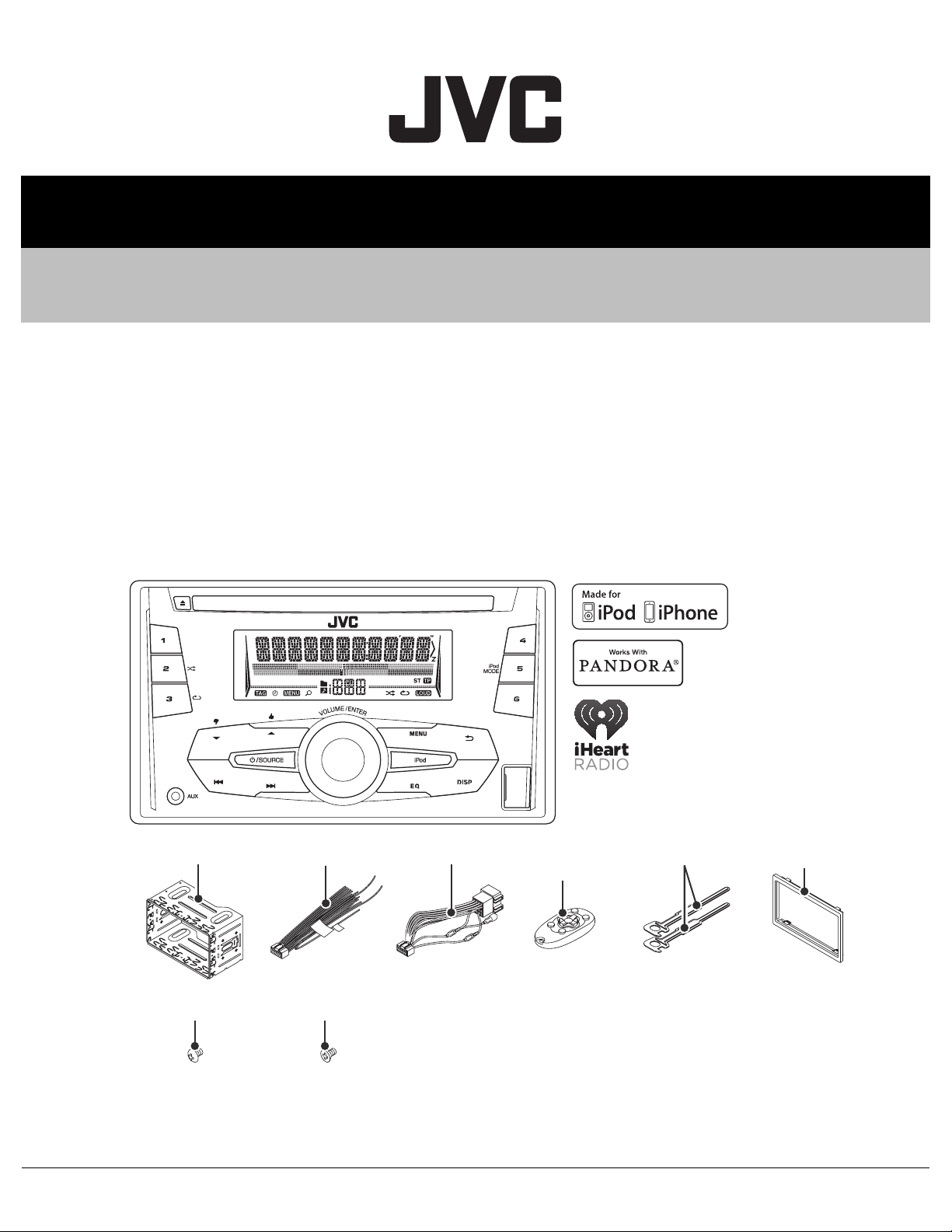
SERVICE MANUAL
MA578<Rev.002>20149SERVICE MANUAL
KW-R510E, KW-R510EE, KW-R510EN,
KW-R510EU, KW-R510EY, KW-R510U,
KW-R510UT, KW-R515U, KW-R710E,
KW-R710EN, KW-R710EY, KW-R710J,
KW-R710U, KW-R710UT
CD RECEIVER
Sleeve assy
(LV22876-001A)
Screw
(QYSDSP5008ZA) x8
COPYRIGHT © 2014 JVC KENWOOD Corporation
DC cord
(QAM1329-001)
Screw
(QYSSSP5008ZA) x8
Lead free solder used in the board (material: Sn-Ag-Cu, melting point: 219 Centigrade)
Lead free solder used in the board (material: Sn-Cu, melting point: 230 Centigrade)
COPYRIGHT © 2014 JVC KENWOOD Corporation
DC cord
(QAM1345-003)
Remocon unit
(RM-RK52C)
(LV45516-001A) x2 (GE20366-001A)
Trim plateLever
No.MA578<Rev.002>
2014/9
Page 2
SPECIFICATION
For US
TUNER
FM Frequency Range 87.9 MHz to 107.9 MHz (200 kHz step)
87.5 MHz to 108.0 MHz (50 kHz step)
Channel Space Selection 50 kHz/200 kHz
Usable Sensitivity (S/N = 26 dB) 8.2 dBf (0.71 µV/75 Ω)
Quieting Sensitivity(DIN S/N = 46 dB) 17.2 dBf (2.0 µV/75 Ω)
Frequency Response (±3 dB) 30 Hz to 15 kHz
Signal-to-Noise Ratio (MONO) 64 dB
Stereo Separation (1 kHz) 40 dB
AM Frequency Range 530 kHz to 1 700 kHz (10 kHz step)
531 kHz to 1 611 kHz (9 kHz step)
Channel Space Selection 9 kHz/10 kHz
Usable Sensitivity (S/N = 20 dB) 29 dBµ (28.2 µV)
CD player
Laser Diode GaAIAs
Digital Filter (D/A) 8 times over sampling
Spindle Speed 500 rpm - 200 rpm (CLV)
Wow & Flutter Below measurable limit
Frequency Response (±1 dB) 20 Hz - 20 kHz
Total Harmonic Distortion (1 kHz) 0.01%
Signal-to-Noise Ratio (1 kHz) 105 dB
Dynamic Range 90 dB
Channel Separation 85 dB
MP3 Decode Compliant with MPEG-1/2 Audio Layer-3
WMA Decode Compliant with Windows Media Audio
USB
USB Standard USB 1.1, USB 2.0 (Full speed)
Compatible Devices Mass storage class
File System FAT12/ 16/ 32
Maximum Supply Current DC 5 V 1 A
MP3 Decode Compliant with MPEG-1/2 Audio Layer-3
WMA Decode Compliant with Windows Media Audio
WAV Decode Linear-PCM
Auxiliary
Frequency Response (±3 dB) 20 Hz - 20 kHz
Input Maximum Voltage 1 200 mV
Input Impedance 30 kΩ
Audio
Maximum Output Power 50 W × 4
Full Bandwidth Power(at less than 1 % THD) 22 W × 4
Speaker Impedance 4 Ω - 8 Ω
Preout Level/Load (CD) 2 500 mV/10 kΩ load
Preout Impedance ≤ 600 Ω
General
Operating Voltage (10.5 V - 16 V allowable) 14.4 V
Maximum Current Consumption 10A
Operating Temperature Range 0°C to + 40°C
Installation Size (W × H × D) 180 mm × 100 mm × 158 mm (7-1/8" × 4" × 6-1/4")
Weight 1.25 kg (2.75 lbs)
• Subject to change without notice.
(No.MA578<Rev.002>)2/23
Page 3
For Europe
TUNER
FM Frequency Range 87.5 MHz to 108.0 MHz (50 kHz step)
Usable Sensitivity (S/N = 26 dB) 0.71 µV/75 Ω
Quieting Sensitivity(DIN S/N = 46 dB) 2.0 µV/75 Ω
Frequency Response (±3 dB) 30 Hz to 15 kHz
Signal-to-Noise Ratio (MONO) 64 dB
Stereo Separation (1 kHz) 40 dB
AM Frequency Range MW : 531 kHz to 1 611 kHz (9 kHz step)
LW : 153 kHz to 279 kHz (9 kHz step)
Usable Sensitivity (S/N = 20 dB) MW : 28.2 µV
LW : 50 µV
CD player
Laser Diode GaAIAs
Digital Filter 8 times over sampling
Spindle Speed 500 rpm - 200 rpm (CLV)
Wow & Flutter Below measurable limit
Frequency Response (±1 dB) 20 Hz - 20 kHz
Total Harmonic Distortion (1 kHz) 0.01%
Signal-to-Noise Ratio (1 kHz) 105 dB
Dynamic Range 90 dB
Channel Separation 85 dB
MP3 Decode Compliant with MPEG-1/2 Audio Layer-3
WMA Decode Compliant with Windows Media Audio
USB
USB Standard USB 1.1, USB 2.0 (Full speed)
Compatible Devices Mass storage class
File System FAT12/ 16/ 32
Maximum Supply Current DC 5 V 1 A
MP3 Decode Compliant with MPEG-1/2 Audio Layer-3
WMA Decode Compliant with Windows Media Audio
WAV Decode Linear-PCM
Auxiliary
Frequency Response (±3 dB) 20 Hz - 20 kHz
Input Maximum Voltage 1 200 mV
Input Impedance 30 kΩ
Audio
Maximum Output Power 50 W × 4
Output Power (DIN 45324, +B = 14.4 V) 30 W × 4
Speaker Impedance 4 Ω - 8 Ω
Preout Level/Load (CD) 2 500 mV/10 kΩ load
Preout Impedance ≤ 600 Ω
General
Operating Voltage 14.4 V (10.5 V - 16 V allowable)
Maximum Current Consumption 10A
Operating Temperature Range 0°C to + 40°C
Installation Size (W × H × D) 182 mm × 112 mm × 158 mm
Weight 1.5 kg
• Subject to change without notice.
(No.MA578<Rev.002>)3/23
Page 4
SPECIFICATION
For ASIA
TUNER
FM Frequency Range 87.5 MHz to 108.0 MHz (50 kHz step)
Usable Sensitivity (S/N = 26 dB) 8.2 dBf (0.71 µV/75 Ω)
Quieting Sensitivity(DIN S/N = 46 dB) 17.2 dBf (2.0 µV/75 Ω)
Frequency Response (±3 dB) 30 Hz to 15 kHz
Signal-to-Noise Ratio (MONO) 64 dB
Stereo Separation (1 kHz) 40 dB
AM Frequency Range Band 1 (MW): 531 kHz to 1 611 kHz (9 kHz step)
Band 2 (SW1): 2 940 kHz to 7 735 kHz (5 kHz step)
Band 3 (SW2): 9 500 kHz to 10 135 kHz (5 kHz step), 11 580 kHz to 18 135 kHz (5 kHz step)
Channel Space Selection Band 1: 9 kHz
Band 2/3: 5 kHz
Usable Sensitivity (S/N = 20 dB) MW: 29 dBµ (28.2 µV)
SW: 30 dBµ (32 µV)
CD player
Laser Diode GaAIAs
Digital Filter (D/A) 8 times over sampling
Spindle Speed 500 rpm - 200 rpm (CLV)
Wow & Flutter Below measurable limit
Frequency Response (±1 dB) 20 Hz - 20 kHz
Total Harmonic Distortion (1 kHz) 0.01%
Signal-to-Noise Ratio (1 kHz) 105 dB
Dynamic Range 90 dB
Channel Separation 85 dB
MP3 Decode Compliant with MPEG-1/2 Audio Layer-3
WMA Decode Compliant with Windows Media Audio
USB
USB Standard USB 1.1, USB 2.0 (Full speed)
Compatible Devices Mass storage class
File System FAT12/ 16/ 32
Maximum Supply Current DC 5 V 1 A
MP3 Decode Compliant with MPEG-1/2 Audio Layer-3
WMA Decode Compliant with Windows Media Audio
WAV Decode Linear-PCM
Auxiliary
Frequency Response (±3 dB) 20 Hz - 20 kHz
Input Maximum Voltage 1 200 mV
Input Impedance 30 kΩ
Audio
Maximum Output Power 50 W × 4
Full Bandwidth Power(at less than 1 % THD) 22 W × 4
Speaker Impedance 4 Ω - 8 Ω
Preout Level/Load (CD) 2 500 mV/10 kΩ load
Preout Impedance ≤ 600 Ω
General
Operating Voltage (10.5 V - 16 V allowable) 14.4 V
Maximum Current Consumption 10A
Operating Temperature Range 0°C to + 40°C
Installation Size (W × H × D) 180 mm × 100 mm × 158 mm
Weight 1.5 kg
• Subject to change without notice.
(No.MA578<Rev.002>)4/23
Page 5
SECTION 1
PRECAUTION
1.1 Safety Precautions
(1) This design of this product contains special hardware and
many circuits and components specially for safety purposes. For continued protection, no changes should be made
to the original design unless authorized in writing by the
manufacturer. Replacement parts must be identical to
those used in the original circuits. Services should be performed by qualified personnel only.
(2) Alterations of the design or circuitry of the product should
not be made. Any design alterations of the product should
not be made. Any design alterations or additions will void
the manufacturers warranty and will further relieve the
manufacture of responsibility for personal injury or property
damage resulting therefrom.
(3) Many electrical and mechanical parts in the products have
special safety-related characteristics. These characteristics are often not evident from visual inspection nor can the
protection afforded by them necessarily be obtained by using replacement components rated for higher voltage, wattage, etc. Replacement parts which have these special
safety characteristics are identified in the Parts List of Service Manual. Electrical components having such features
are identified by shading on the schematics and by ( ) on
the Parts List in the Service Manual. The use of a substitute
replacement which does not have the same safety characteristics as the recommended replacement parts shown in
the Parts List of Service Manual may create shock, fire, or
other hazards.
(4) The leads in the products are routed and dressed with ties,
clamps, tubings, barriers and the like to be separated from
live parts, high temperature parts, moving parts and/or
sharp edges for the prevention of electric shock and fire
hazard. When service is required, the original lead routing
and dress should be observed, and it should be confirmed
that they have been returned to normal, after reassembling.
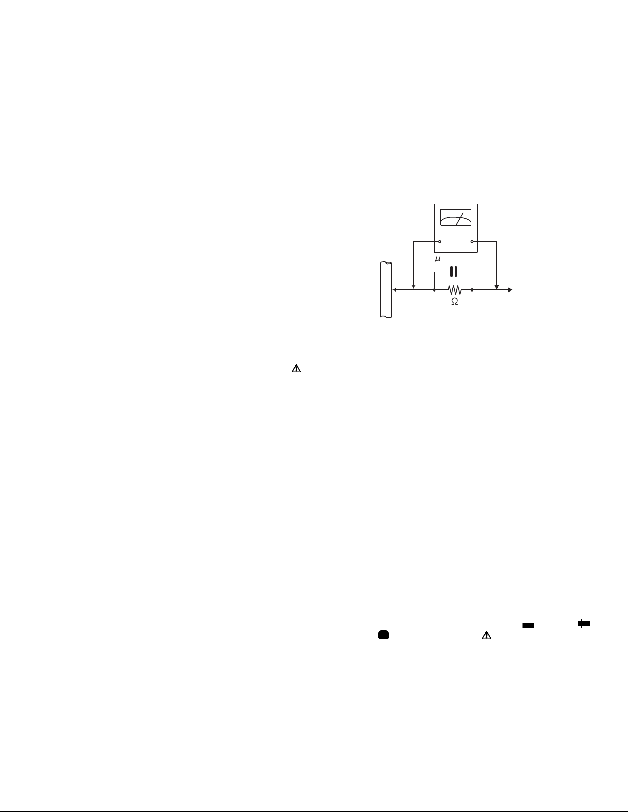
(5) Leakage shock hazard testing
After reassembling the product, always perform an isolation check on the exposed metal parts of the product (antenna terminals, knobs, metal cabinet, screw heads,
headphone jack, control shafts, etc.) to be sure the product
is safe to operate without danger of electrical shock.Do not
use a line isolation transformer during this check.
• Plug the AC line cord directly into the AC outlet. Using a
"Leakage Current Tester", measure the leakage current
from each exposed metal parts of the cabinet, particularly any exposed metal part having a return path to the
chassis, to a known good earth ground. Any leakage current must not exceed 0.5mA AC (r.m.s.).
• Alternate check method
Plug the AC line cord directly into the AC outlet. Use an
AC voltmeter having, 1,000Ω per volt or more sensitivity
in the following manner. Connect a 1,500Ω 10W resistor
paralleled by a 0.15µF AC-type capacitor between an ex-
posed metal part and a known good earth ground.
Measure the AC voltage across the resistor with the AC
voltmeter.
Move the resistor connection to each exposed metal
part, particularly any exposed metal part having a return
path to the chassis, and measure the AC voltage across
the resistor. Now, reverse the plug in the AC outlet and
repeat each measurement. Voltage measured any must
not exceed 0.75 V AC (r.m.s.). This corresponds to 0.5
mA AC (r.m.s.).
AC VOLTMETER
(Having 1000
ohms/volts,
or more sensitivity)
0.15 F AC TYPE
Place this
probe on
1500 10W
Good earth ground
1.2 Warning
(1) This equipment has been designed and manufactured to
meet international safety standards.
(2) It is the legal responsibility of the repairer to ensure that
these safety standards are maintained.
(3) Repairs must be made in accordance with the relevant
safety standards.
(4) It is essential that safety critical components are replaced
by approved parts.
(5) If mains voltage selector is provided, check setting for local
voltage.
1.3 Caution
Burrs formed during molding may be left over on some parts
of the chassis.
Therefore, pay attention to such burrs in the case of preforming repair of this system.
1.4 Critical parts for safety
In regard with component parts appearing on the silk-screen
printed side (parts side) of the PWB diagrams, the parts that are
printed over with black such as the resistor ( ), diode ( )
and ICP ( ) or identified by the " " mark nearby are critical
for safety. When replacing them, be sure to use the parts of the
same type and rating as specified by the manufacturer.
(This regulation dose not Except the J and C version)
1.5 Remote control
The Lithium battery is in danger of explosion if replaced incorrectly. Replace it only with the same or equivalent type.
each exposed
metal part.
(No.MA578<Rev.002>)5/23
Page 6
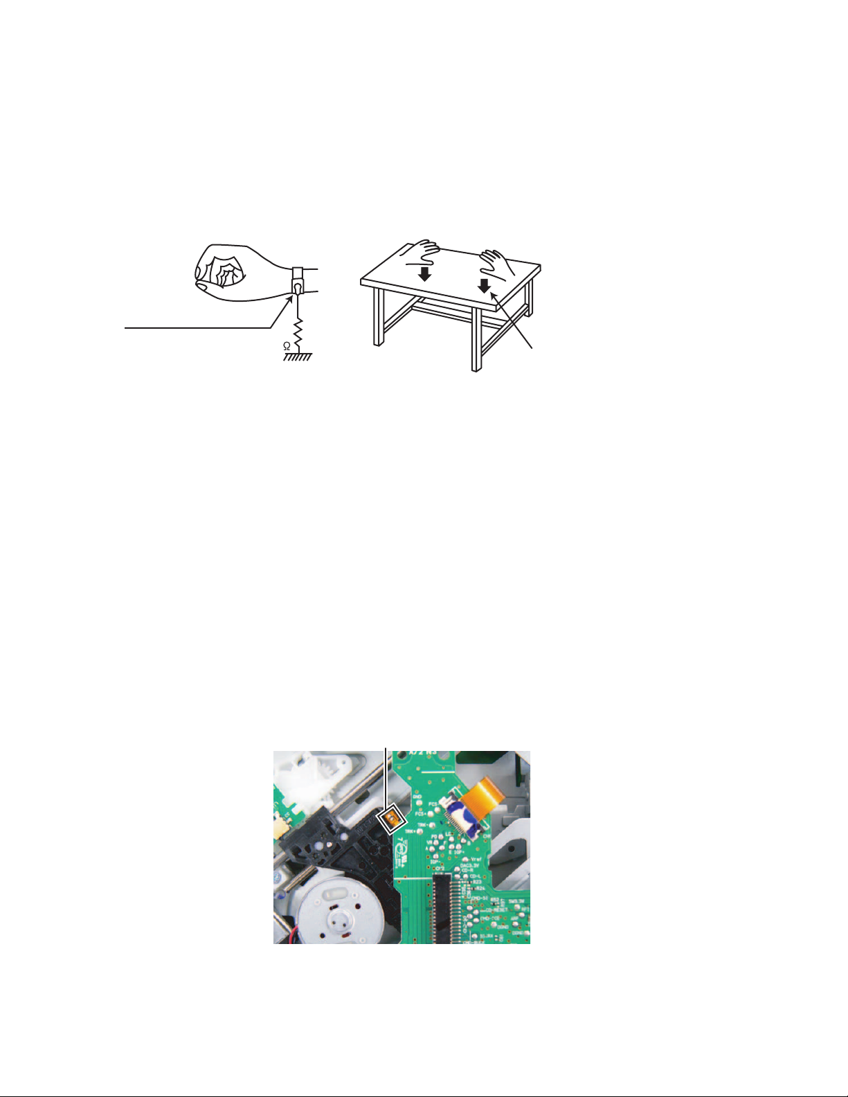
1.6 Preventing static electricity
Electrostatic discharge (ESD), which occurs when static electricity stored in the body, fabric, etc. is discharged, can destroy the laser
diode in the traverse unit (optical pickup). Take care to prevent this when performing repairs.
1.6.1 Grounding to prevent damage by static electricity
Static electricity in the work area can destroy the optical pickup (laser diode) in devices such as laser products.
Be careful to use proper grounding in the area where repairs are being performed.
(1) Ground the workbench
Ground the workbench by laying conductive material (such as a conductive sheet) or an iron plate over it before placing the
traverse unit (optical pickup) on it.
(2) Ground yourself
Use an anti-static wrist strap to release any static electricity built up in your body.
(caption)
Anti-static wrist strap
1M
Conductive material
(conductive sheet) or iron plate
(3) Handling the optical pickup
• In order to maintain quality during transport and before installation, both sides of the laser diode on the replacement optical
pickup are shorted. After replacement, return the shorted parts to their original condition.
(Refer to the text.)
• Do not use a tester to check the condition of the laser diode in the optical pickup. The tester's internal power source can easily
destroy the laser diode.
1.7 Handling the traverse unit (optical pickup)
(1) Do not subject the traverse unit (optical pickup) to strong shocks, as it is a sensitive, complex unit.
(2) Cut off the shorted part of the flexible cable using nippers, etc. after replacing the optical pickup. For specific details, refer to the
replacement procedure in the text. Remove the anti-static pin when replacing the traverse unit. Be careful not to take too long a
time when attaching it to the connector.
(3) Handle the flexible cable carefully as it may break when subjected to strong force.
(4) I t is not possible to adjust the semi-fixed resistor that adjusts the laser power. Do not turn it.
1.8 Attention when traverse unit is decomposed
*Please refer to "Disassembly method" in the text for the pickup unit.
• Apply solder to the short land sections before the card wire is disconnected from the connector on the servo board. (If the card wire
is disconnected without applying solder, the pickup may be destroyed by static electricity.)
• In the assembly, be sure to remove solder from the short land sections after connecting the card wire.
SOLDER
(No.MA578<Rev.002>)6/23
Page 7
1.9 Important for laser products
1.CLASS 1 LASER PRODUCT
2.CAUTION :
(For U.S.A.) Visible and/or invisible class II laser radiation
when open. Do not stare into beam.
(Others) Visible and/or invisible class 1M laser radiation
when open. Do not view directly with optical instruments.
3.CAUTION : Visible and/or invisible laser radiation when
open and inter lock failed or defeated. Avoid direct
exposure to beam.
4.CAUTION : This laser product uses visible and/or invisible
laser radiation and is equipped with safety switches which
prevent emission of radiation when the drawer is open and
the safety interlocks have failed or are defeated. It is
dangerous to defeat the safety switches.
5.CAUTION : If safety switches malfunction, the laser is able
to function.
6.CAUTION : Use of controls, adjustments or performance of
procedures other than those specified here in may result in
hazardous radiation exposure.
!
Please use enough caution not to
see the beam directly or touch it
in case of an adjustment or operation
check.
(No.MA578<Rev.002>)7/23
Page 8
SECTION 2
SPECIFIC SERVICE INSTRUCTIONS
2.1 How to repair a fuse pattern
2.1.1 Purpose of fuse pattern
In order to prevent serious damage on the circuit, fuse pattern is prepared on the GND line of RCA Terminal. This damage may
take due to improper part replacement with a external equipment via RCA line.
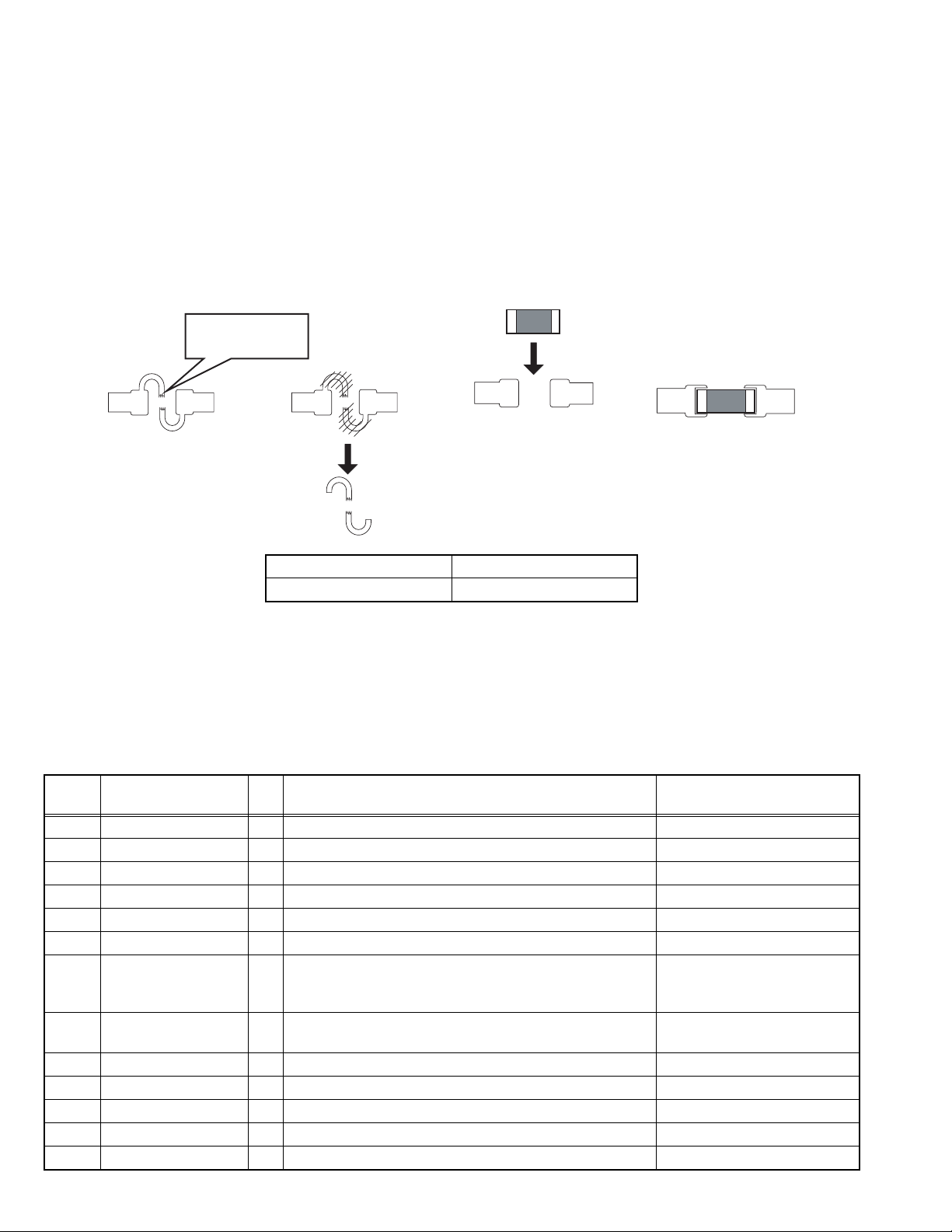
2.1.2 Repair Procedure
(1) Check the shorted circuit at the meltdown point.
Need to clean up if the shorted circuit or carbonization happen at the fuse pattern.
(2) Add following parts on the fuse pattern.
(3) Check output level.
Meltdown point
Parts Number SPEC
F53-0513-08 4A
2.1.3 After finished repair
Due to improper part replacement, this meltdown occurs.
Thus please notice following information when the unit is return to your customer.
Things to be checked before installing the unit.
(1) Check the GND line of external amplifier or other equipment which must connect properly.
(2) Check whether the GND line is not short-circuited with the battery terminal. (do not short-circuit these lines)
2.2 MICROCOMPUTER’S TERMINAL DESCRIPTION
IC701 (R5S726A0D216FP) on MAIN PWB ASSY
Pin No. Pin Name I/O Application Processing / Operation / De-
scription
1 LCD_INH O LCD Reset L: Reset ON / H: Reset OFF
2 BT_RST O BT Reset Output (For BT model) L: Reset ON / H: Reset OFF
2 NC O No Use (For non BT model) keep L output setting
3 PVcc - Power supply for I/O circuits
4 NRST O LSI Reset Signal (L: Reset) L: Reset ON / H: Reset OFF
5Vss -GND
6 PON_PANEL O Supply Control to Panel L: ON / H: OFF (within
11minutes after Acc OFF: L /
>11minutes after Acc OFF: H)
7 DC_ERR2 I Detect DC Clip (for ST Power Amp IC) L: DC Error ON / H: DC Error
OFF
8 PWIC_MUTE O Muting Output for Power Amp IC L: Mute ON / H: Mute OFF
9 LCD_CE O LCD Driver IC Chip Enable Output (for LCD Model)
10 Vss - GND
11 LCD_CLK O LCD CLK Output
12 Vcc - Power supply
(No.MA578<Rev.002>)8/23
Page 9

Pin No. Pin Name I/O Application Processing / Operation / De-
scription
13 RGB_CLK O I2C Clock Output for RGB Driver (For RGB Model)
13 NC O No Use (for non RGB model)
13 PCB_TEST_MODE_RXI PCB Test Mode RX
14 LCD_DATA_OUT O LCD DATA Output (for LCD Model)
14 LCD_RGB_DATA_OUTO LCD and RGB DATA Output (for RGB Model)
14 PCB_TEST_MODE_TXO PCB Test Mode TX
15 DEBUG_1B O For Debug
16 PVcc - Power supply for I/O circuits
17 BT_SYS_DATA I BT Data Input (For BT model only)
17 NC O No Use (for non BT model)
18 Vss - GND
19 BT_BT_DATA O BT Data Output (For BT model only)
19 NC O No Use (for non BT model)
20 Vcc - Power supply
21 DEBUG_1A O For Debug
21 SXM_PWR O Power Supply for SXM (For SXM model only) L: PWR Off / H: PWR On
22 SXM_RxD I SXM Data Input (For SXM model only)
22 NC O No Use (for non SXM model)
23 DEBUG_1C O For Debug
23 SXM_TxD O SXM Data Output (For SXM model only)
24 PWIC_STBY O Output to Power On Power Amp IC L: Standby / H: Play
25 PON_USB O Enable Output for High Side Switch L: HisideSW OFF / H: HisideSW
ON
26 PON_DCDC6V O Enable Output for DC-DC Regulator
27 PSW I CD Mecha Position Setting SW (Reset Switch)
28 PVcc - Power supply for I/O circuits
29 FREQ_SEL O Frequency Select Pulse: Power On / L: Power Off
30 Vss - GND
31 ENC2 I Volume Encoder Pulse Input 2
32 ENC1 I Volume Encoder Pulse Input 1
33 REMO I Remocon Input L (Pulse): Remote control data /
H: Standby
34 LCD_DATA_IN I LCD DATA Intput (for LCD Model)
35 SW1 I CD Mecha SW1
35 DEBUG_2A O For Debug
36 PVcc - Power supply for I/O circuits
37 CKIO O No Use (System Clock Output to External Devices [for LCD
Model])
38 Vss - GND
39 RESET I Reset Input
40 Vss - GND
41 PLLVcc - Power supply for PLL
42 PAN_DET I Panel Detection input L: Panel Attached / H: Panel De-
tached
(No.MA578<Rev.002>)9/23
Page 10

Pin No. Pin Name I/O Application Processing / Operation / De-
scription
42 NC I No Use (for non detachable model)
43 Vcc - Power supply
44 EXTAL I High Speed Clock 12MHz
45 XTAL O High Speed Clock 12MHz
46 Vss - GND
47 Vss - GND
48 PVcc - Power supply for I/O circuits
49 D-0 I/O USB Data- 0
50 D+0 I/O USB Data+ 0
51 ASEMD I ASE Mode Select Pin
52 STEERING_REMO1 I OE Remote In 1 (for DOP models)
52 NC I No Use (For KWD Model)
53 STEERING_REMO2 I OE Remote In 2 (for DOP models)
53 NC I No Use (For KWD Model)
54 STAGE2 I Model Selecting Input 2
55 STAGE1 I Model Selecting Input 1
56 TEL_MUTE I Tel Mute Detection Input (for JVC Model)
56 LINE_MUTE I Line Mute Detection Input (For KWD Model)
56 NC I No Use (For non support Tel mute model)
57 DC_ERR1 I Detect DC Offset Error from EVOL IC L:DC Error ON / H:DC Error
OFF
58 Avss - GND
59 Avcc - Power Supply
60 Avref - Reference Power Supply
61 TRST I Debugging Interface. Reset Input.
62 ASEBRKAK/ASEBRK I/O Emulator Break Mode Acknoledge/Break Input
63 TDO O Debugging Interface. Serial Output for Instructions and Data
64 TDI I Debugging Interface. Serial Input for Instructions and Data
65 TMS I Debugging Interface. Test Mode Select Signal Input.
66 TCK I Debugging Interface. Test Clock Input.
67 NC O No Use
68 NC I No Use
69 PVcc - Power supply for I/O circuits
70 SPBCLK O FLASH SPI Multi I/O Bus Clock output
71 Vss - GND
72 SPBSSL O FLASH SPI Multi I/O Bus Slave Select Output
73 SPBIO0 I/O FLASH SPI Multi I/O Bus I/O Data 0
74 SPBIO1 I/O FLASH SPI Multi I/O Bus I/O Data 1
75 SPBIO2 I/O FLASH SPI Multi I/O Bus I/O Data 2
76 Vss - GND
77 SPBIO3 I/O FLASH SPI Multi I/O Bus I/O Data 3
78 Vcc - Power supply
79 MD_CLK I Clock Mode Set (Power ON Reset) EXTAL Pin Input Clock
Ranges from 10 to 12 MHz
80 MD_BOOT I BOOT Mode Set L: Boot mode 0 / H: Boot mode 1
(No.MA578<Rev.002>)10/23
Page 11

Pin No. Pin Name I/O Application Processing / Operation / De-
scription
81 DRV_MUTE O Motor Driver Mute Control Signal L: Output OFF (mute)/ H: Output
ON (not mute)
81 DEBUG_2C O For Debug
82 PVcc - Power supply for I/O circuits
83 REG2-1 O Control Output for CTRL2 from regulator IC
84 Vss - GND
85 BT_MUTE I BT Mute L: Mute OFF / H: Mute ON
85 NC O No Use (For non BT model) keep L output setting
86 Vcc - Power supply
87 REG1-1 O Control Output for CTRL1 from regulator IC
88 REG1-2 O Control Output for CTRL1 from regulator IC
89 REG2-2 O Control Output for CTRL2 from regulator IC
90 MUTE O Muting Output for Evol & Line Out L: Mute ON / H: Mute OFF
91 SCL_EVOL I/O I2C Clock 240kHz for E-Vol
91 SCL_EP I/O I2C Clock 240kHz for E2PROM
91 SCL_TU I/O I2C Clock 240kHz for Tuner
92 SDA_EVOL I/O I2C Data for E-Vol
92 SDA_EP I/O I2C Data for E2PROM
92 SDA_TU I/O I2C Data for Tuner
93 IPOD_SCL O iPod Authentication IC I2C Clock Clock speed 23kHz
93 NC O No Use (For non-iPod Model)
94 IPOD_SDA O iPod Authentication IC I2C Data
94 NC O No Use (For non-iPod Model)
95 NC O No Use
96 ILM_SW O Enable Output for ILL 11V L: ILM SW OFF / H: ILM SW ON
97 CD_DSP_SW O CD DSP Switch L: Other sources / H: CD USB
SD source
98 DIM_IN I Dimmer Control Input (for JVC Model) L: Dimmer Detect ON / H: Dim-
mer Detect OFF
98 NC O No Use (For KWD Model) keep L output setting
99 PS1 I Power Save 1 (ACC Detection) L: Acc ON / H: Acc OFF
100 Vss - GND
101 PVcc - Power supply for I/O circuits
102 PS2 I Power Save 2 (BU Detection) L: Battery ON / H: Battery OFF
103 BCLK I Servo DSP Data Bit Clock
104 LRCK I Servo DSP Data Word Clock
105 SRDATA I Servo DSP Data Input
106 SRDATIN O Servo DSP Data Output
107 Vss - GND
108 MCLK O Microcontroller Command Clock Signal
109 Vcc - Power supply
110 MDATA O Microcontroller Command Data Signal
111 MLD O Microcontroller Command Load Signal
112 PVcc - Power supply for I/O circuits
113 STAT I DSP Status Signal
114 Vss - GND
(No.MA578<Rev.002>)11/23
Page 12
Pin No. Pin Name I/O Application Processing / Operation / De-
scription
115 DRV_CNT O Loading Motor Control Output
116 BEEP O Output for Beep Tone Generator H(Pulse): BEEP / L: OFF
117 DRV_Lo/Ej O Loading Motor Control Output
118 PCB_TEST_MODE I PCB Test Mode Switch L: Normal Mode / H: Check
Mode (After Reset software
need to check the pin input. If
detect high it should enter Serial
Number mode)
119 SW2 I CD Mecha SW2
119 DEBUG_2B O For Debug
119 Field Test 2 O RDS data log output (standby for field test)
120 BLKCK I Sub-Code Block Clock Signal
120 Field Test 1 O RDS data log output (standby for field test)
SECTION 3
DISASSEMBLY
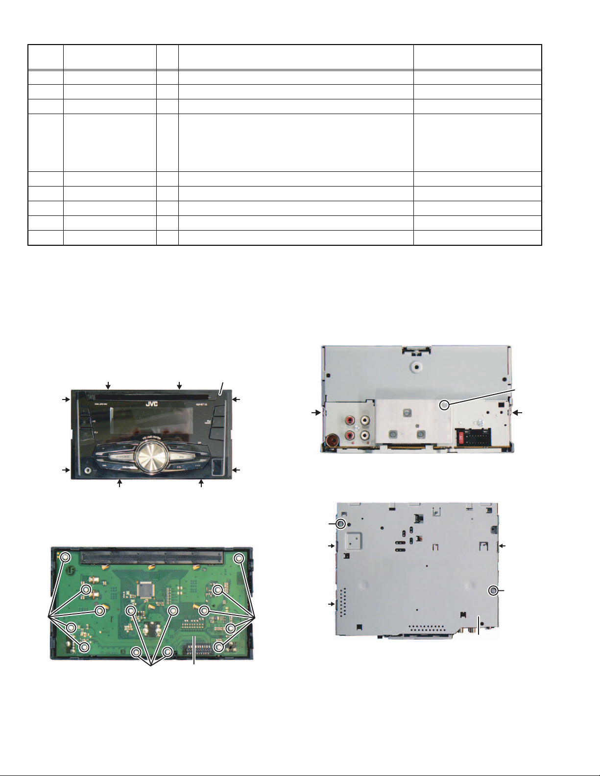
3.1 Main body
3.1.1 Removing the SW PWB (See Fig.1 and 2)
(1) Disengage the 8 hooks, and remove the Front chassis.
(See Fig.1)
HOOK HOOK
HOOK HOOK
HOOK HOOK
HOOK
Fig.1
(2) Remove the Volume knob.
Remove the 14 screws A, a
(3)
(See Fig.
2)
nd
remove the SW PWB.
FRONT CHASSIS
HOOK
A
3.1.2 Removing the Main PWB (See Fig.3 to 6)
(1)
Remove the 1 screw B and 2 screws C. (See Fig.
3)
B
C
Fig.3
(2) Remove the 2 screws D. (See Fig.4)
(3) Disengage the 3 hooks, and remove the Bottom cover.
(See Fig.4)
D
HOOK
C
HOOK
D
HOOK
A
A
Fig.2
BOTTOM COVER
Fig.4
SW PWB
(No.MA578<Rev.002>)12/23
Page 13
(4) Disconnect the FFC wire from connector CN1. (See Fig.5)
CN1
Fig.5
(5) Disengage the 2 hooks, and remove the Main PWB.
(See Fig.6)
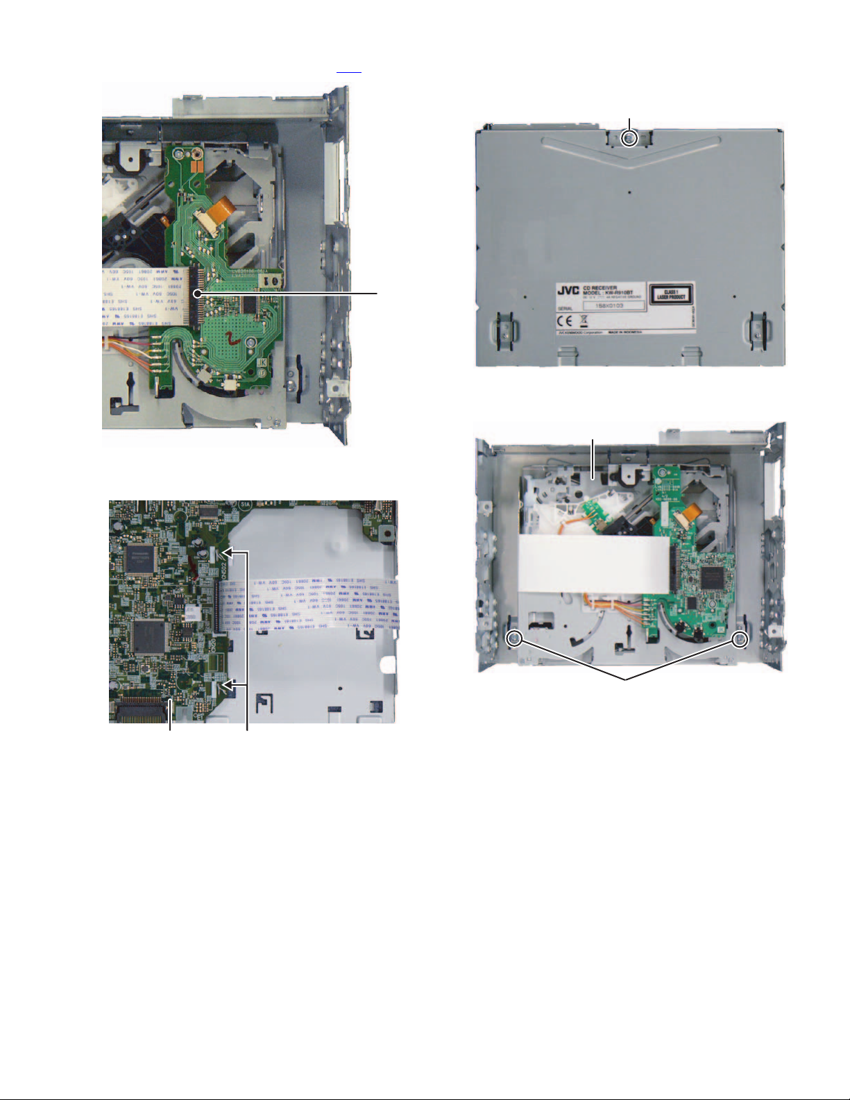
3.1.3 Removing the CD mechanism (See Fig.7)
(1) Remove the 1 screw E.(See Fig.7)
E
Fig.7
(2) Remove the 2 screws F, and remove the CD mechanism.
(See Fig.8)
CD MECHANISM
MAIN PWB HOOK
Fig.6
F
Fig.8
(No.MA578<Rev.002>)13/23
Page 14
3.2 CD mechanism
• NOTICE FOR HANDRIG OF MECHANISM ASSY
OK
Handle CHASSIS part.
• NOTICE FOR HANDRIG OF FEED MOTR ASSY
CAUTION: For mounting FEEDMOTOR ASSY, DON'T bump this part.
Because handling may cause this part easily deformed.
FEED MOTOR
WORM 1
NG
Do not stay MECHANISM ASSY in upside-down condition
for 1 hour and more.
NG
Do not touch P.C.B..
Do not touch DAMPER.
• NOTICE FOR HANDRIG OF ROLLER LEVER ASSY
OK
Do not handle roller part.
NG
• NOTICE FOR CLAMPER ASSY OF PICK UP ASSY
OK NG
Do not handle
the clamper part.
Do not touch
PICK UP ASSY.
NG
TOP SIDE BOTTOM SIDE
DO NOT TOUCH AREA
DO NOT TOUCH HOLES, MOTOR, DAMPER, PCB, FFC, OPU AND WIRE.
• THESE PARTS NEED CAUTION OF HANDLING
CAUTION:
Don't touch the following parts in particular by the hand which
touched grease. (It becomes a cause of traction problem)
CAUTION PARTS
HC TURN TABLE TRIGGER ARM
ROLLER DISC GUIDE
• NOTICE FOR HANDRIG OF MD CHASSIS ASSY
NG
OK
Handle CHASSIS part.
Do not handle the
turn table part.
• NOTICE FOR HANDRIG OF PICK UP ASSY
OK NG
Do not handle the lens part.
(No.MA578<Rev.002>)14/23
Page 15
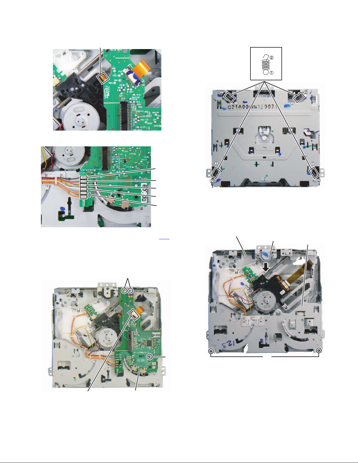
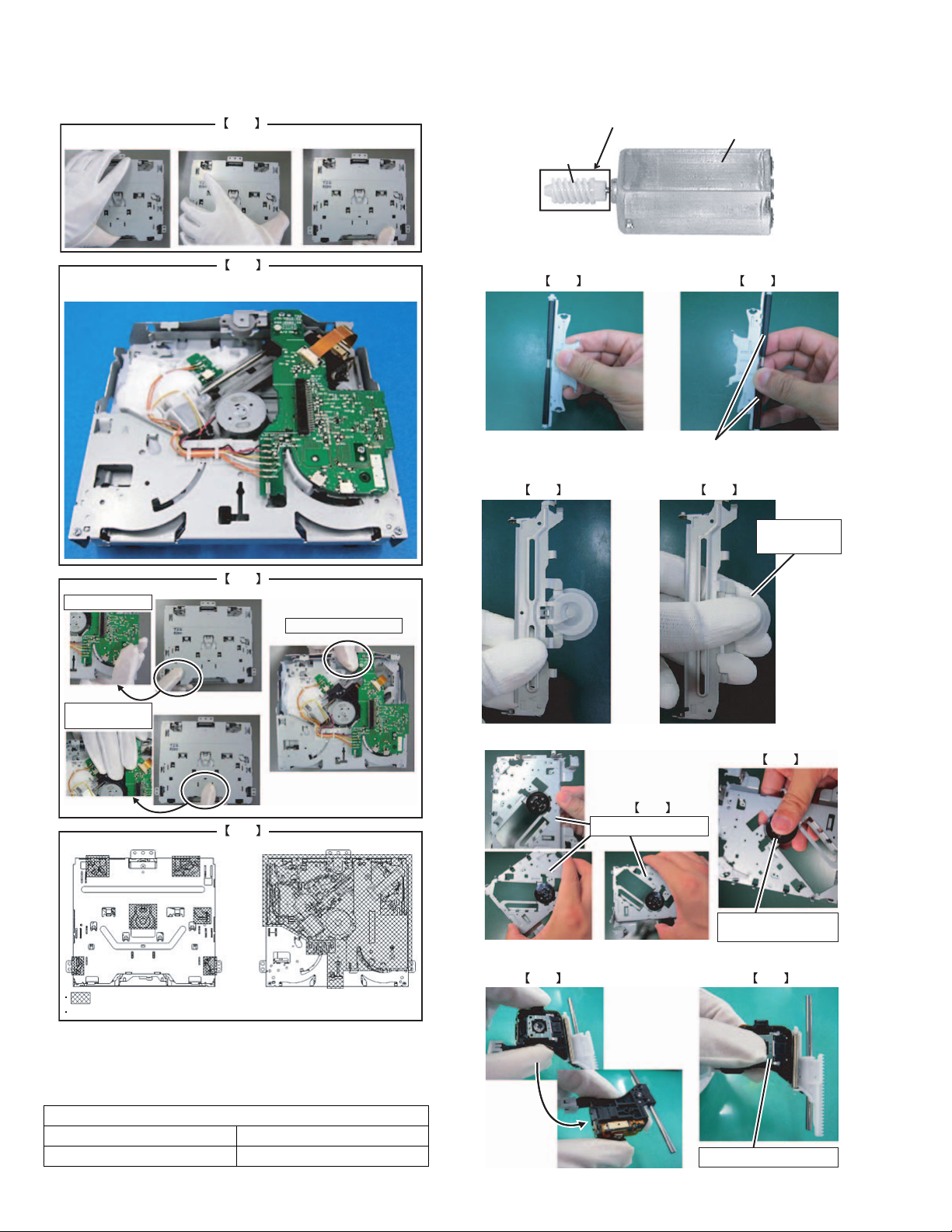
3.2.1 Removing the CD Player unit (See Fig.1 to 3)
(1) Solder the short land on the Pickup. (See Fig.1)
SOLDER
Fig.1
(2) Remove the 6 wires from the CD Player unit. (See Fig.2)
Black
Red
Yellow
Orange
Fig.2
(3) Disconnect the FPC wire from the connector CN1
Player unit). (See Fig.3)
(4) Remove the 3 screws A attaching the CD Player unit.
(See Fig.3)
(5) Remove the CD Player unit. (See Fig.3)
White
Orange
(CD
3.2.2 Removing the Traverse mechanism (See Fig.4, 5)
(1) Remove the 4 springs from the traverse mechanism.
(See Fig.4)
Spring
Fig.4
(2) Remove the 2 screws B attaching the Lower chassis.
(See Fig.5)
(3) Remove the Damper in the direction of the arrow.
(See Fig.5)
(4) Remove the Traverse mechanism. (See Fig.5)
Traverse mechanism
Damper
Lower chassis
CN1
Fig.3
A
CD Player unit
A
B
Fig.5
(No.MA578<Rev.002>)15/23
Page 16
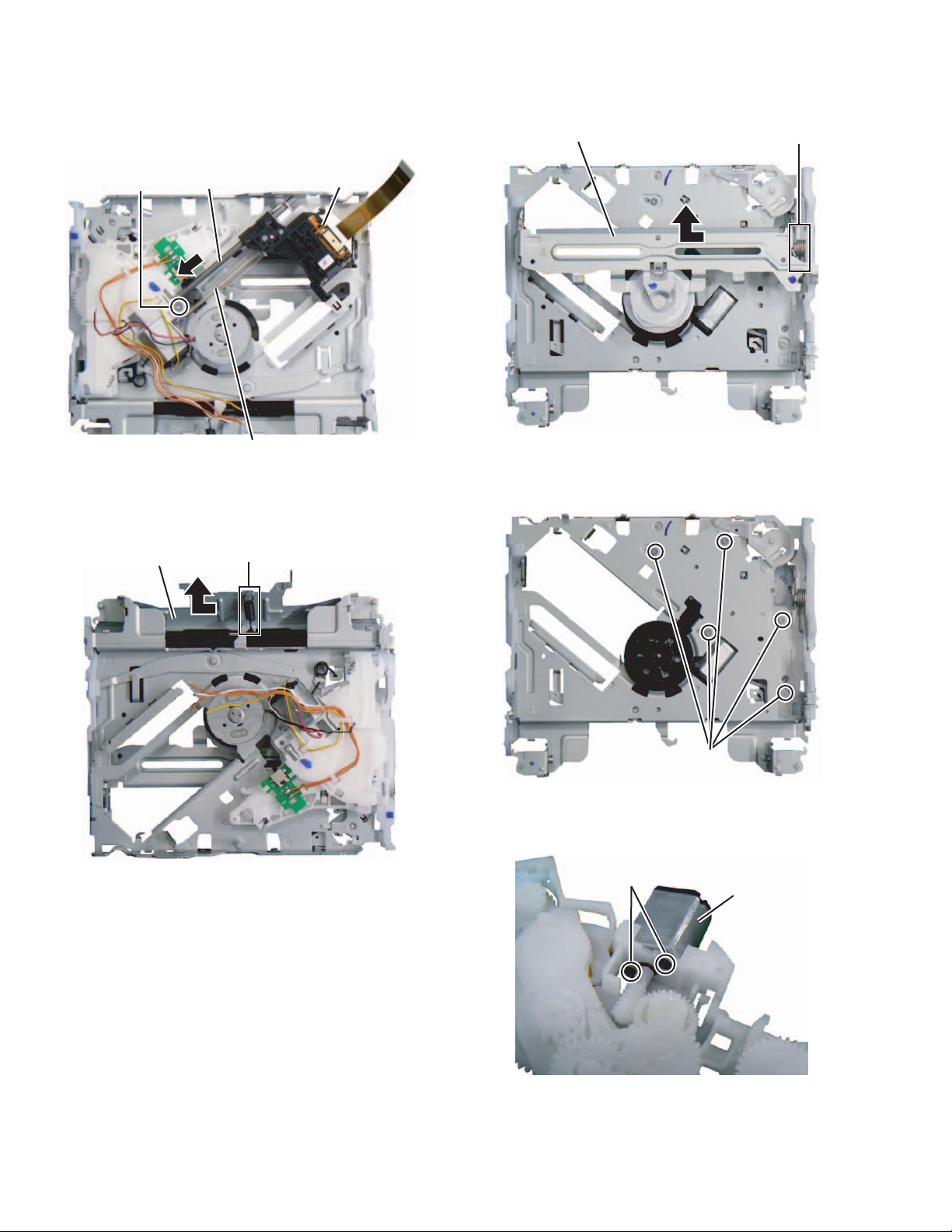
3.2.3 Removing the Pickup assy (See Fig.6)
(1) Remove the 1 screw C.
(2) Remove the Main shaft in the direction of the arrow.
(3) Remove the Spring.
(4) Remove the Pickup assy.
3.2.5 Removing the Clamp arm assy (See Fig.8)
(1) Remove the Spring.
(2) Remove the Clamp arm assy in the direction of the arrow.
Clamp arm assy
Spring
Main shaft
C
Spring
Fig.6
3.2.4 Removing the Roller lever assy (See Fig.7)
(1) Remove the Spring.
(2) Remove the Roller lever assy in the direction of the arrow.
Roller lever assy
Spring
Pickup assy
Fig.8
3.2.6 Removing the Feed motor (See Fig.9, 10)
(1) Remove the 5 screws D attaching the Feed motor assy.
(See Fig.9)
Fig.7
D
Fig.9
(2) Remove the 2 screws E attaching the Feed motor.
(See Fig.10)
(3) Remove the Feed motor. (See Fig.10)
E
Feed motor
Fig.10
(No.MA578<Rev.002>)16/23
Page 17
SECTION 4
ADJUSTMENT
4.1 Service Test mode
4.1.1 Default status immediately after the mode activation
Operating Key: [MENU] + [] (7sec) Press and hold.
4.1.2 How to release each Test mode
• Reset
•Acc off
• Power off
• Panel Detach
4.1.3 Mode content
Syscon shall display the following information after entering this mode. The operation shown below shall be workable.
Display content Detail
S R V T E S T
The display is released when another operation is executed.
4.1.4 Common operation mode for all sources
means Press and hold.
Operation Display content Detail
EQ/
PHONE*/
iPOD*/
CD error
information display
mode
Transit to CD error information display mode
DAB*()
MENU
Syscon version
display
S Y S #
@ @ @
# = Display of destination.
J = USA
R = EUROPE
E = EASTERN-EUROPE
U = OTHERS(e.g. ASIA)
@@@ = Syscon version number
Power ON duration
display
2
P O N T M 0 H X X
00 - 50 are displayed in " XX ".
For less than 1 hour, the display is
indicated per 10 minutes.
00001 - 10922 are displayed in " XXXXX ".
2
Power ON
duration clear
P O N T M X X X X X
P O N T M 0 H 0 0
MAX 10922 (hours).
Clear Power ON duration by pressing
for 2 seconds when Power ON duration
is displayed.
Disc operation
duration display
C D T M 0 H X X
1(*)()
00 - 50 are displayed in " XX ".
For less than 1 hour, the display is
indicated per 10 minutes.
(Not applicable for mechaless models)
00001 - 10922 are displayed in " XXXXX ".
C D T M X X X X X
MAX 10922 (hours). (Not applicable for
mechaless models)
1(*)()
Disc operation
duration clear
C D N T M 0 H 0 0
Clear Disc operation duration by pressing
for 2 seconds when it is displayed (Only
the displayed media is cleared).(Not
applicable for mechaless models)
For less than 1 hour, the display is
indicated per 10 minutes.
DISP()
DISP
()
Disc eject number
of times
Disc eject number
of times clear
E J C N T X X X X X
E J C N T 0 0 0 00
00001 - 99999 are displayed in
"XXXXX"
Clear Disc Eject number of times by
pressing for 2 seconds when it is displayed.
*This includes all media (CD, USB, iPod, SD) action duration.
Not applicable for mechaless models
(No.MA578<Rev.002>)17/23
Page 18

4.1.5 CD Error Information Display Mode (Not applicable for mechaless models)
Operation Display content Detail
CD mecha error
log display
Mecha error history 1,2,3 (latest)
# = History No. (1,2,3)
XX : kind of errors, " -- " when there is
none.
00: No Error
04: TOC read Error
M E C H E R #AXX
05: Unknown CD
06: Heat Error
0A: Update Error
0D: Hold Error
15: Unknown Disc
99: Mecha Error
CD load error
information display
L O A D E R # X X
Load error switch 1,2
# = History No. (1,2)
XX: numbers of errors, " -- " when there
is none
History No. 2 is un-used
CD eject error
information display
Eject error switch 1,2,3,4
# =History No. (1,2,3,4)
XX: numbers of errors, " -- "when there
Move
between
DISP
(Forward
search)
i t e m w i t h
[] / []
CD time code error
count information
display (count skip)
E J E C T E R # X X
C N T L O S E
C D D A XX
is none
History No.3 is un-used
History No.1: Eject before SW1 is on.
History No.2: Eject until SW1 and SW2
is on.
History No.3: Eject between SW2 on
and Eject end
CD-DA error count number information
CD-DA error count numbers
XX: numbers of errors and " -- " when
there is none
Can only be checked via debugger by
jap member
CD-ROM (compressed file) error count
numbers
XX: numbers of errors and " -- " when
C D R O M X X
there is none
Can only be checked via debugger by
jap member
CD time code error
count information
display (no count
update)
C N T S T A Y
C D D A XX
CD time code error count information
(count not updated) mode display
CD-DA error count numbers
XX: numbers of errors and " -- " when
there is none
CD-ROM (compressed file) error count
numbers
C D R O M X X
XX: numbers of errors and " -- " when
there is none
EQ/
PHONE*/
iPOD*/
CD error
information clear
CD error information all clear Clear CD error information by pressing
M E C H A E R 1 - -
for 2 seconds when it is displayed.
DAB*
EQ/
Mode release CD error information display mode release Back to default status, All lights on
PHONE*/
iPOD*/
DAB*
*Only for model without EQ key
(No.MA578<Rev.002>)18/23
Page 19

4.2 Service Information Clear Mode
4.2.1 Default status immediately after the mode activation
* The receiver is connected with the DC power supply (with the power supply turned off).
Operating Key: [BACK] + [POWER] Press and hold + DC power supply turned ON
4.2.2 How to release each Test mode
Cleared information changes will take place only after reset.
4.2.3 Mode content
After entering this mode, Syscon shall clear the information stored for service and output the result to the display tube.
CD will be ejected upon process ended.
Preset Frequencies and Tagging (HD models) information shall be cleared.
Display content Detail
I N I T IAL I Z E
D A T A C L R O K
Data Clear in Progress (Only application for BT model)
When normal end
When error end
D A T A C L R N G
Display blinks with 250ms interval.
The following table shows the data that is cleared.
Information for data clearing Detail Storage area
CD mecha log display E2PROM
CD load error information display E2PROM
CD mecha information
CD eject error information display E2PROM
CD time code error count information display (count skip) E2PROM
CD time code error count information display (no count update) E2PROM
Power ON duration display E2PROM
Service information
CD operation duration display E2PROM
CD EJECT number of times display E2PROM
Force Power OFF information display E2PROM
DC error information
DC error 1 display (wrong connection & other detection information in detecting duration) E2PROM
DC error 2 display (capacitor leakage detection number information) E2PROM
Tuner Area Setting E2PROM
Preset information
Preset Frequency E2PROM
Preset PI code E2PROM
Preset HD Station Name and Sub-Channel Number (HD models) E2PROM
SXM Preset Channel SID E2PROM
Sirius XM information
SXM Lock Channel SID E2PROM
SXM Channel Lock Code E2PROM
SXM Mature Channel Setting E2PROM
Tagging information (HD models) Token data memory index E2PROM
Bluetooth information
(Sent Initialize command to BT
Module)
Pairing Information FLASH ROM
in BT Module
Phonebook Entried of unit FLASH ROM
in BT Module
Call History information of unit FLASH ROM
in BT Module
DAB Information DAB Preset Service ID E2PROM
DAB Preset Channel ID & Sub Channel ID E2PROM
(No.MA578<Rev.002>)19/23
Page 20

4.3 DC error information mode
4.3.1 Default status immediately after the mode activation
* The receiver is connected with the DC power supply (with the power supply turned off).
Operating Key: [MENU] + [] Press and hold + DC power supply turned ON
4.3.2 How to release each Test mode
• Reset
•Acc off
• Power off
• Panel Detach
4.3.3 Mode content
Syscon shall display the following information after entering this mode. The operation shown below shall be workable.
Display content Detail
D C E R R
D C O K
When DC error is detected (in case that one of capacitor leakage,
wrong connection or other detection is found).
When DC error is not detected (in case that none of capacitor leakage, wrong connection or other detection is found).
4.3.4 Mode operation specification
means Press and hold
Operation Display content Detail
FSKIP
FSKIP
DC ERR1
display
DC ERR1
clear
D C 1 E R R
D C 1 O K
D C 1 O K
When wrong connection & DC error in other detection duration is detected.
When wrong connection & DC error in other detection duration is not detected.
Clear detection information when wrong connection & DC error in other detection duration is
displayed.(Clear data flash)
BSKIP
BSKIP
DC ERR2
display
DC ERR2
clear
D C 2 4
D C 2 0
Display detecting number of times in capacitor
leakage detection duration (0 - 4)
Clear number of times for detection information
in capacitor leakage detection duration.(Clear
data flash)
(No.MA578<Rev.002>)20/23
Page 21

4.4 DC offset error description
A
4.4.1 Indication of DC Offset
3-DIGIT DISPLAY 11-DIGIT DISPLAY
Display
Mode
Display
Character
[DC 1 Error]
i1 2 3
M I S WIR I N G
MISWIRING
[DC 1 Error]
HC K WIR I N G
CHK WIRING
[DC 1 Error]
HT E N R E S E T
THEN RESET
[DC 1 Error]
UNIT
DC
Offset
[DC 2 Error]
W A NR I N G
WARNING
[DC 2 Error]
HC K WIR I N G
CHK WIRING
[DC 2 Error]
HT E N R E S E T
THEN RESET
[DC 2 Error]
UNIT
4.4.2 DC Offset detection circuit design
•Purpose:
To prevent breakdown, when occur DC offset between speaker output "+" and "-".
• Target:
Detect DC offset, then stop the Power Amp operation and shift
to specified condition.
4.4.3 Possible causes of DC offset at speaker output lines
(1) Mis-connection for Speaker output for example touch to car
body or battery line.
(2) Current leak of coupling capacitor for Power IC input.
(3) Current leak of AC-GND capacitor for Power IC AC-GND.
(4) Capacitor shorted of above parts due to foreign object.
C-tc
E-Vol
Win_TC
Win_In
DC Error
C-in
C-in
R3
C-in
C-in
C-ac2C-ac1
Sw5V
R2
R1
C3
R4
Audio Pwr Amp
In 1
In 2
In 3
In 4
AcGnd
Offset Detect
Out
Micon
ADC In
Comment
45 67891011231
Display for 2 sec
Display for 2 sec
Display for 2 sec
U NIT
Display for 2 sec
Then loop to "MISWIRING"
Display for 2 sec
Display for 2 sec
Display for 2 sec
U NIT
Display for 2 sec
Then loop to "WARNING"
4.4.4 Type of checking
4.4.4.1 To detect DC Offset Error
• Mis-connection
- Short any one speaker out line to GND or Vcc
• Capacitor leak
- Parallel 330kΩ to either any one of coupling cap or AC-GND
capacitor (to simulate current leakage of capacitor)
- Shorted either any one of coupling capacitor or AC-GND capacitor.
4.4.5 Detection Timing chart
1.5sec or more
0.8sec
0.7sec or more
1.0sec
Capacitor leak
detection period
Other (miss detection etc.)
detection period
PWIC_STBY
PWIC_MUTE
UD_MUTE
2.0sec or more
Missconnect
detection period
50ms
or more
(No.MA578<Rev.002>)21/23
Page 22

4.4.6 Manipulate after detect DC Offset
• If detected error 10 consecutive times, and 10th error occurred
in "Mis-connect detection period", judge as "Mis-connect".
• If detected error 10 consecutive times, and 10th error occurred
in "Capacitor leak detection period", judge as "Capacitor leak ".
• If detected error 10 consecutive times, and 10th error occurred
in "Other detection period" and detected another 10 errors consecutively, then judge as "Other".
• If judge as "Mis-connect".
- turn off speaker output.
- - display "MISWIRING", check wiring connection then reset.
- key access disable except button of Eject, Reset and service
mode
- record error in EEPROM "DC1 ERR"
- the product is able to be recovered by Reset button.
• If judge as "Capacitor leak ".
- turn off speaker output.
- display "WIRING", check wiring connection then reset.
- key access disable except button of Eject, Reset and service
mode
- record error in EEPROM "DC2 #" (# means counter number)
- the product can be recovered by pressing the Reset button
before the capacitor leak error counter reach "DC2 4".
After that, only clear the counter back to "0" can recover the
product.
• If judge as "Other" (manipulation same as mis-connect)
SECTION 5
TROUBLESHOOTING
5.1 How to cancel DC offset error
Check to be sure the terminals of the speaker leads are covered with insulating tape properly, then reset the product.
If an error message does not disappear even after a reset, there is a need for internal repair.
5.2 How to clear DC offset error recorded in EEPROM
Refer to “4.3 DC error information mode”.
(No.MA578<Rev.002>)22/23
Page 23

JVC KENWOOD Corporation
CE Segment 2967-3, Ishikawa-machi, Hachioji-shi, Tokyo, 192-8525, Japan
(No.MA578<Rev.002>)
Printed in Japan
VSE
Page 24

SCHEMATIC DIAGRAMS
15
CD RECEIVER
KW-R510E KW-R510EE KW-R510EN
KW-R510EU KW-R510EY KW-R510U
KW-R510UT KW-R515U KW-R710E
KW-R710EN KW-R710EY KW-R710J
KW-R710U KW-R710UT
(No.MA578<Rev.002>)1/
Page 25

■ PRECAUTIONS ON SCHEMATIC DIAGRAMS
z Due to the improvement in performance, some part numbers shown in the circuit diagrams
may not agree with those indicated in the Parts List.
z The parts numbers, values and rated voltage etc. in the Schematic Diagrams are for
reference only.
z Since the circuit diagrams are standard ones, the circuits and circuit constants may be
subject to change for improvement without any notice.
■ PRECAUTIONS ON PARTS LIST
z
The parts identified by the symbol are critical for safety. Whenever replacing these parts, be sure to
use specified ones to secure the safety.
z
The parts not indicated in this Parts List and those which are filled with lines --- in the Parts No.
columns will not be supplied.
z
P.W. BOARD Ass'y will not be supplied, but those which are filled with the Parts No. in the Parts No.
columns will be supplied.
z
When ordering chips, screws etc., place bulk orders (unit of tens) whenever possible to improve
shipping efficiency.
z
There are cases where the actual implemented parts in the sets and the service parts are different.
When ordering parts, make sure to refer to the Parts List.
■
PRECAUTIONS ON SERVICE
Certain parts of the power circuits and the GNDs differ according to the models. Care must be
taken for the following points as the differences are indicated separately in the LIVE GND ( ) and
the ISOLATED (NEUTRAL) GND ( ).
1. Do not touch the LIVE GND, or do not touch the LIVE GND and the ISOLATED (NEUTRAL)
GND at the same time. It may cause an electric shock.
Before pulling out the chassis or other parts, make sure to pull out the power cord from the
wall outlet first.
2. Do not short circuit between the LIVE GND and ISOLATED (NEUTRAL) GND, or never
measure the LIVE GND and ISOLATED (NEUTRAL) GND at the same time using measuring
instruments (oscilloscope, etc.). It may blow fuses or damage other parts.
■ DEVIATION TOLERANCE RANGE
DEVIATION TOLERANCE RANGE
F G J K M N R H Z P
± 1% ± 2% ± 5% ±10% ±20% ±30%
+30%
-10%
+50%
-10%
+80%
-20%
+100%
-0%
15
(No.MA578<Rev.002>)2/
Page 26

6V
DC DC
IC981
IC901
REGULATOR
FLASH
IC840
RESET
IC720
EEPROM
IC710
MICON
IC701
DRIVER
LCD
IC661
PROCESSING
IC540
CD SIGNAL
POWER AMP
IC301
E-VOLUME
IC161
iPOD
IC80
BTL
TUNER
IC1
IC1
J602
CN603
SWITCH PWB ASSY
MAIN PWB ASSY
CD MECHA PWB ASSY
CN1
CN502
D-
D+
RGB
S2 TO S51
COM4
COM3
COM2
COM1
REMOCON
VOL2
VOL1
RGBCLK
LCDDA/RGBDA
RGBCL
KEY2
KEY1
KEY0
LCDDA/RGBDA
LCDCE
LCDCLK
RGB DRIVER
F-AUXG
F-AUXR
F-AUXL
F-AUXG
F-AUXR
F-AUXL
D-
D+
LCD
USB
RGB LEDs
REMOCON
AUX
ENCODER
KEY MATRIX
J182
CN601
DMO
FMO
TRO
FOO
DRV_MUTE
Lo/Ej
CNT
Vref
SW3.3
LD
CD_MD
VT2
VT1
VF2
VF1
PWS
SW2
SW1
TRK -
TRK +
FOCUS -
FOCUS +
TRK -
TRK +
FOCUS -
FOCUS +
LD
CD_MD
VT1, VT2
VF1, VF2
LOAD -
LOAD +
FEED -
FEED +
SW2
SW1
PSW
SW1,SW2
MOTOR
SPINDLE
MOTOR
LOAD&FEED
SWITCH
POSITION SET
PICK UP
CN701
D-
D+
USB
PON_
PON_6V
FREQ_SEL
RC LPF
CTRL2
CTRL1
ACC
ACC DET
BU DET
MEMORY
OFFSER 2
DC ERR
MUTE
ANT
MEMORY
EXT
REMOTE
ANT
HSS
MUTE
TEL
CD_PON
ACC DET
SURGE DET
BU-DET/
ERR
DC
ANT
J1
J321
CN901
DC CORD
RST
DC DC3.3V
3.3V
SW
3.3V_CD
LDO
CDR
CDL
RR-
RR+
RL-
RL+
SCL TU/EVOL
SDA TU/EVOL
F-AUXG
F-AUXR
F-AUXL
AMP STBY
AMP MUTE
SWR
SWL
RR OUT/SWR
FR OUT
RL OUT/SWL
FL OUT
RR
FR
RL
FL
FR-
FR+
FL-
FL+
TUR
TUL
CIRCUIT
MUTE
CP_SDA
CP_SCL
SPBSSL
SPBCLK
SPBIO3
SPBIO2
SPBIO1
SPBIO0
SCL TU/EVOL
SDA TU/EVOL
DATA IN
MCLK
MLD
MDATA
NRST
STAT
BCKOUT
SRDATA
LRCK
BLKCK
LD
CD_MD
VT2
VT1
VF2
VF1
DMO
FMO
TRO
FOO
Vref
CNT
Lo/Ej
DRVMUTE
PSW
SW2
SW1
MUTE
SD_CMD
SD_CLK
SD_DA
SD_DET
LCDCE
LCDCLK
LCDDA
RGBCLK
REMOCON
VOL2
VOL1
Panel 3.3V
SW
HSS
ILM
SW
PON_USB ILM_SW PON_Panel
BLOCK DIAGRAM
created date:2014-02-27No.MA578
15
(No.MA578<Rev.002>)3/
Page 27

3.
CONDITION---FM MODE.
1. VOLTAGES ARE DC-MEASURED WITH A DIGITAL VOLT METER
WITHOUT INPUT SIGNAL
ALL CAPACITORS ARE 50V OR 25V CERAMIC CAPACITOR.
ALL RESISTORS ARE 1/16W 5% METAL GLAZE RESISTOR.
UNLESS OTHERWISE SPECIFIED.
COMPONENTS IN ( ) INDICATE NOT USE.
( )CD MODE.AM MODE.
2.
ALL RESISTANCE VALUES ARE IN OHM.
TU33V
3.3V
*
1.5V
1.5V
0V
0V
1.5V
0V
3.3V
3.3V
0V
3.3V3.3V
0V
3.3V
1.2V
1.2V
2.8V
1.5V
1.5V
3.3V
3.3V
3.3V
3.3V
0V
0V
0V
0V
0V
0V
0V
0V
0V
3.3V
3.3V 0V
3.3V
0V
0V
3.3V
3.3V
0V
0V
0V
0V
0V
0V
0V
0V
0V
0V
0V
0V
0V
0V
0V
0V
0V
3.3V
0V
0V
0.6V
0V
0V
0.6V
0V 0V
3.3V
0V
0V
3.3V
3.3V
0V
0V
1.25V
3.3V
3.3V
0V
0V
1.25V
3.3V
3.3V
3.3V
3.3V
3.3V
3.3V
0V
0V
0V
0V
0V
0V
0V
0V
0V
0V
0V
0V
0V
0V
0V
0V
0V
0V
0V
0V
0V
3.3V
0V
1.25V
3.3V
3.3V
3.3V0V3.3V
3.3V
0V
0V0V0V
0V0V0V
3.3V
0V
1.25V
3.3V
3.3V
3.3V
1.6V
0V0V0V
0V
0V
0V
1.25V
1.25V
1.9V
1.9V
3.3V
3.3V
3.3V
3.3V
3.3V
3.3V
3.3V
0V
0V
0V
0V
0V
0V
0V
0V
0V
3.3V
3.3V
*
1.5V
3.3V
0V
3.3V
3.3V
3.3V
3.3V
3.3V
3.3V
1.5V
1.5V
1.5V
0V0V0V
0V0V0V
0V
0V
0V
1.25V
0V
3.3V
3.3V
3.3V
(3.3V)0V
0V
3.3V
1.25V0V3.3V
3.3V
NOT IN USE
* POWER CORD ASS'Y
8.4V
0V
3.3V
5.2V 5.2V
0V
0V
0V0V0V
0V
0V
0V
0V
0V
0V
0V
5.2V
14.3V
4.9V
3.3V
1.6V
0V
1.1V
1.0V
3.3V
3.3V
3.3V
3.3V
3.3V
3.3V
3.3V
3.3V
3.3V
3.3V
3.3V
3.3V
0V
4.0V
4.0V
4.0V
4.0V
4.0V
4.0V
4.0V
8.2V
3.3V
3.3V
3.3V
3.3V
3.3V
3.3V
0V
3.3V
6.2V
3.3V
3.3V
14.3V
14.3V
0V
14V
3.3V
14.3V
(3.3V)/1V
1.2V
(7.9V)
1.2V
0V
3.3V0V7.1V
3.5V
7.1V
14.2V
7.1V0V7.1V
7.0V
6.9V
6.9V
6.9V
0V
6.9V
7.1V
7.1V0V7.1V
14.2V
7.1V
3.2V
7.1V0V3.3V
0V
4.6V
3.3V
3.3V
3.3V
4.6V
0V
4.6V
4.6V
SGND
CD_GND
SGND
CD_GND
REMOTE OUT
ANT
MAIN PWB:GEB10370A
10V
LDO_1.25V
LINE MUTE
P.IC MUTE
SW3.3V
HSS_USB
IPOD CP CIRCUIT
EEPROM
RESET
1.7V
3.3V
3.3V
3.3V
3.3V
3.3V
0V
0V
3.3V
3.1V
3.1V
0V
0V
0V
0V
DCDC
DEBUGGING
FLASH
VDD
SW1
PON_USB
MGND
MGND
P.IC_GND
MGND
MGND
MICON_GND
DCDCGND
EVOL_GND
TEL_MUTE
ILM_10V
LCD_DA_I
MEMORY
MEMORY
MEMORY
MEMORY
OFFSET
SPBSSL
SPBIO1
SPBIO2
FL+
FL+
FR-
MICON1.25V
REMO
V6
DRST
SDATUVR
DC_ERR1
USB5V
AUDIO9V
AUDIO9V
AUDIO9V
AUDIO9V
IPOD_SDA
SXM_PWR
SXM_RX
TU3.3
PWIC_STBY
SW3.3V
SW3.3V
MLD
SPBCLK
BEEP
LCD_DA_O
IPOD_SCL
LCD_DA_O
LCD_CLK
ILM_SW
LCD_CE
LCD_INH
ENC2
PON_PANEL
RGB_CLK
ENC1
REMO
D-
AUX-G
AUX-R
D+
AUX-L
RESET
PON_PANEL
CD_PON
DIM_IN
D-
SPBCLK
ENC2
ENC1
OE1
OE2
LCD_INH
CD8V
CD8V
SRDATA
OE1
OE2
RESET
RESET
BU_DET
CTRL2
RR-
FR-
RL+
DRST
LCD_DA_I
BCLK
DRV_CNT
REMO
BLKCK
DRV_MUTE
DRST
DC_ERR1
RGB_CLK
SPBIO0
SPBIO3
RL/SUBL
RR/SUBR
SW2
DRV_LO_EJ
ILM_SW
PON_DCDC
VDD6V
MDATA
MCLK
SRDAIN
STAT
LRCK
DIM_IN
TU.R
PSW
CD_PON
FL-
RL-
RR+
FR+
OFFSET
FROUT
FLOUT
RROUT
ACC_DET
BU_DET
CTRL1
RESET
PON_DCDC
CD.R
SXI_AR
TEL_MUTE
FREQ_SEL
SXM_PWR
CD.L
SCLTUVR
SDATUVR
SRDAIN
SRDATA
BLKCK
CD.R
STAT
MLD
MDATA
MCLK
LRCK
BCLK
SW2
SW1
MUTE
BU_DET
E_MUTE
DRV_MUTE
PSW
NRST
DRV_LO_EJ
DRV_CNT
ACC_DET
FREQ_SEL
NRST
SXM_RX
DC_ERR2
SXM_TX
CTRL1
PWIC_MUTE
PON_USB
MUTE
SCLTUVR
LCD_CE
LCD_CLK
D+
IPOD_SCL
SPBSSL
CTRL2
IPOD_SDA
SPBIO0
SPBIO1
SPBIO2
SPBIO3
RL/SUBL
SDATUVR
SXI_AL
SXI_AG
SXI_AL
SXM_TX
SCLTUVR
SDATUVR
TU.L
CD.L
AUX-R
AUX-G
AUX-L
SCLTUVR
RR/SUBR
SXI_AG FLOUT
SXI_AR
E_MUTE
RLOUT
TU.R
FROUT
RROUT
E_MUTETU.L
RL+
FL-
RL-
FR-
RR-
FR+
RR+
RLOUT
PWIC_MUTE
DC_ERR2
PWIC_STBY
BEEP
RLOUT
FLOUT
FROUT
RROUT
GND4
GND5
sure to use the specified one.
When replacing those parts make
Parts are safety assurance parts.!
!
!
!
!
18 17
MEMORY
16
ILL
15
TEL MUTE
14
OE REMOTE
13
REAR RIGHT (+)
12
REAR RIGHT (-)
11
REAR LEFT (-)
10
REAR LEFT (+)
9
FRONT LEFT (+)
8
FRONT LEFT (-)
7
FRONT RIGHT (-)
6
FRONT RIGHT (+)
5
*ANTENNA
4
REMOTE/P-CON
3
ACC
2
GND
1
QNZ0607-001
CN901
!
!
!
!
!
12Mhz
NAX1243-001X
X701
9.216MHZ
QAX0969-001Z
X1
NAF0029-002X
D1
AR
SW33
INH
GND1
AUDFB
P33
LDI
V115
REM2
LCLK
D-
RCLK
RST1
CE
VOL2
5V
TXM
AL
AG
AC
TH
AUDCD
RL
DI
TU.R TU.L
VDD
REM
ASEMD
TU33
HOLD
V125
DO
DB1C
V6I
TCK
GND2
BUP
DB1B
DB2A
RXM
L
DB2B
SUBR
S2
R
DB2C
BDET
TMUTE
DIMMER_IN
S5
ILMFB
FB
SDET2
S6
HSSIN
D+
ERR1
S10
RST2
DB1A
ASEBRK
WP
ILM
TMS
MEM
VOL1
SDA
SCL
TDO
ANT
CS
ADET
TM
OE
TDI
CLK
SUBL
TRST
FR
SDET
RR
AIN
FL
TH30
1/4W
0
R486
470
R100
R912
R715
*
0
R952
R711
R101
R102
68k
R892
R917
R432
1/4W0
R307
0
1/4W
R170
3.3k
R709
R916
47k
R104
1/4W
470R424
R918
*
1/4W
0
R907
1/4W
0
R800
1/4W
470R425
1.6k
R706
R909
1.6kR707
0
R915
R919
R105
1/4W
1kR773
47kR727
47k
R103
1/4W
47k
R978
47k
R739
47k
R738
1/4W
2.2k
R718
4.7k
R904
R164
*
0
R85
1/4W
4.7k
R911
10k
R921
100kR884
22k
R883
*
R725
5.1
R303
1/4W
6.8k
R980
4.7k
R886
4.7k
R885
22k
R882
33k
R881
100k
R710
1/4W
6.8k
R979
1/8W
47k
R971
1/8W
68k
R970
0
R986
100k
R976
33k
R975
22k
R974
33k
R973
100k
R972
R162
0
R809
22k
R977
56k
R969
1/4W
0
R449
R163
R30
1/8W
0
R434
1/8W
0
R468
1/4W
0
R463
1/4W
0
R442
0
R418
0
R431
0
R21
R161
0.5%
20k
R990
10
R803
10R802
0
R404
0
R301
10
R905
47k
R419
33R578
33R577
0
R401
10
R20
0.5%
18k
R982
R716
12k
R893
100
R806
4.7
R5
R300
100k
R807
R14
1.6k
R701
R887
15kR732
100
R805
100
R169
*
100
R80
R714
100
R8
*
100
R81
100
R7
100
R168
1k
R758
1k
R4
1k
R914
1k
R940
10k
R784
1kR721
10kR761
1kR722
10k
R987
15kR731
*
180
R330
180
R250
R350
*
180
R320
180
R260
R12
10k
R717
10k
R989
10k
R171
10k
R891
10kR762
2.2k
R720
2.2k
R719
470
R985
4.7k
R902
2.2k
R804
47k
R411
R253
R340
100kR783
1M
R1
R10
1M
R729
R9
1M
R2
R992
0.5%
4.3k
R984
R983
1.6k
R704
1.6k
R705
910
R708
1.6k
R703
82
R3
R11
4.7R801
47k
R769
47k
R412
R724
47kR749
47k
R415
47kR757
47k
R840
47k
R417
47k
R746
47k
R421
47k
R842
*
R743
*
R742
47k
R991
47k
R414
47k
R409
47k
R420
R744
47k
R413
*
R741
R736
47k
R304
47kR756
R737
R712
22k
R780
47k
R747
47k
R841
47k
R726
*
R745
47k
R748
47k
R735
R408
4.7k
R764
4.7k
R403
*
4.7k
R851
2.2kR763
4.7kR759
4.7k
R765
4.7k
R702
*
4.7kR83
4.7k
R760
*
4.7k
R82
*
4.7k
R84
*
330
R323
R343
330
R781
*
330
R333
R353
330
R262
330
R252
27k
R903
33k
R901
270R776
270R777
2.2M
R740
22k
R251
R351
22k
R261
22k
R941
*
22k
R321
*
22k
R331 R341
2.2k
R302
2.2kR723
2.2k
R988
0
R167
2.2k
R730
R13
22R733
22R734
LTC043TEB-X
Q250
Q320
*
LTC043TEB-X
Q321
Q330
*
LTC043TEB-X
Q331
LTC043TEB-X
Q251
LTA014EEB-X
Q80
LTA024EEB-X
Q782
LTA014YEB-X
Q912
LTA024EEB-X
Q780
LTC024EEB-X
Q941
LTC024EEB-X
Q781
LSCR523UB-X
Q972
Q911
LSCR523UB-X
Q881
LSCR523UB-X
Q970
LSCR523UB-X
Q971
Q910
DSA2001/R/-X
Q940
L161
15u
L981
QQR1927-001
L901
4.7u
L982
4.7u
L941
4.7u
L9
0.12u
L10
1.0u
L8
0.22u
L11
0.47u
L7
0.15u
L6
0.1u
L3
4.7u
L5
NQR0269-017X
L750
L418
L401
NQR0022-005X
L701
NQR0022-005X
L782
NQR0022-005X
L752
NQR0022-005X
L757
NQR0022-005X
L756
NQR0022-005X
L755
NQR0022-005X
L754
NQR0022-005XL780
NQR0022-005XL783
L400
NQR0022-005X
L753
NQR0022-005XL781
NQR0269-030X
L751
NQR0154-006X
L841
NQR0154-006X
L758
1211
T10
10T99T88
T7
7T66T55T44
T3
3T22T11
QNZ0907-001
J801
8
SUB-L7FRONT-L6(REAR-L)
5
4
SUB-R3FRONT-R2(REAR-R)
1
/REAR-R
/REAR-L
*
J321
BLKCK120
DEBUG_2B/FIELD TEST 2/SW2119
PCB_TEST_MODE118
SERIAL_NO_MODE/DRV_Lo/Ej117
BEEP116
DRV_CNT115
Vss114
STAT113
PVcc112
MLD111
MDATA110
Vcc109
MCLK108
Vss107
SRDAIN106
SRDATA105
LRCK104
BCLK103
PS2102
PVcc101
Vss100
PS199
DIM_IN98
CD_DSP_SW97
ILM_SW96
DRST95
IPOD_SDA94
IPOD_SCL93
SDA_EVOL92
SCL_EVOL91
MUTE
90
REG2-289REG1-288REG1-1
87
Vcc
86NC85
Vss
84
REG2-1
83
PVcc
82
DEBUG_2C/DRV_MUTE
81
MD_BOOT
80
MD_CLK
79
Vcc
78
SPBIO3
77
Vss
76
SPBIO275SPBIO174SPBIO0
73
SPBSSL
72
Vss
71
SPBCLK
70
PVcc
69
AUDIO_X168AUDIO_X2
67
TCK
66
TMS
65
TD164TD0
63
ASEBRKAK/ASEBRK
62
TRST
61
AVref 60
AVcc 59
AVss 58
DC_ERR1 57
TEL_MUTE/LINE_MUTE 56
Stage1 55
Stage2 54
STEERING_REMO2 53
STEERING_REMO1 52
ASEMD 51
D+O 50
D-O 49
PVcc 48
Vss 47
Vss 46
XTAL 45
EXTAL 44
Vcc 43
PAN_DET 42
PLLVcc 41
Vss 40
RESET 39
Vss 38
CKIO 37
PVcc 36
DEBUG_2A/FIELD TEST 1/SW1 35
LCD_DATA_IN 34
REMO 33
ENC1 32
ENC2 31
Vss30FREQ_SEL29PVcc28PSW27PON_DCDC6V26PON_USB25PWIC_STBY24SXM_TxD/DEBUG_1C
23
SXM_RxD22SXM_PWR/DEBUG_1A
21
Vcc20NC19Vss18NC17PVcc16DEBUG_1B15LCD_DATA_OUT/PCB_TEST_MODE_TX
14
RGB_CLK/PCB_TEST_MODE_RX
13
Vcc12LCD_CLK11Vss10LCD_CE9PWIC_MUTE8DC_ERR27PON_PANEL6Vss5NRST4PVcc3NC2DRV_INH
1
R5S726A0D216FP
IC701
GND
33
XTAL_IN 32
VSS 31
DAC_L 30
SDA
24
VSSD_IO
23
I2S_SD_IN16
DR_I_DATA15
DAC_R 29
GPIO_0 28
GPIO_1 27
GPIO_2 26
SCL 25
VDDD
22
VSSD
21
i.c.
20
I2S_SD_1
19
I2S_BCK
18
I2S_WS
17
DR_Q_DATA14
DR_BCK13
DR_WS12
DR_BL11
AM_LNA_CAP10
AM_IN_P9
VSSA_RF
8
VDDA_RF
7
FM_RF_IN_P
6
FM_IN_M
5
FM_CAP
4
VBGP
3
VSSA_IFADC
2
VDDA_IFADC
1
TEF6657HN-X
IC1
SE1R1SE1L2SE2R3SE2L4SE3R5SE3L6QD1R7QD1G8QD1L9FD1R+/QD2R10FD1R-/QD2G11FD1L-/QD2G12FD1L+/QD2L13CREF
14
GND
15
OUTSWL
16
OUTSWR
17
OUTLF
18
OUTLR
19
OUTRR
20
OUTRF
21
WINTCWINTC
22
MUTEMUTE
23
VCCVCC
24
SCLSCL
25
SDASDA
26
DCERRDCERR
27
WININ
28
TDA7718B-X
IC161
TAB1
1
OFFDET
2
PWGND1
3
OUT2-
4
STBY
5
OUT2+
6
VCC1
7
OUT1-
8
PWGND2
9
OUT1+
10
SVR
11
IN1
12
IN2
13
SGND
14
IN4
15
IN3
16
ACGND
17
OUT3+
18
PWGND3
19
OUT3-
20
VCC2
21
OUT4+
22
MUTE
23
OUT4-
24
PWGND4
25
HSD
26
TAB2
27
JCV8031
IC301
ANT
14
ILM
1
ILM_F
2
CD
3
AUDIO_F
4
AUDIO
5
CTRL2
6
VCC2
7
CTRL1
8
VCC1
9
GND
10
V6IN
11
VDD
12
13
EXT
15
LV5684NPVD
IC901
9
VCC
8
RST
7
SCL
6
NC55NC4
4
NC3
3
SDA
2
GND
1
*
MFI337S3959-X
IC80
9
VCC
8
BST
7
EN
6
SYNC
5
FB
4
VC
3
GND
2
LX
1
BD9876EFJ-X
IC981
/CS
1
DO
2
/WP
3
GND
4
DI
5
CLK
6
/HOLD
7
VCC
8
W25Q16DVSSIG-X
IC840
A0
1
A1
2
A2
3
GND
4
SDA
5
SCL
6
WP
7
VCC
8
BR24T02FJ-W-X
IC710
OUT
6
ILIM
5
FLAG
4
EN
3
GND
2
IN
1
NCP380HSNAJAA-X
IC982
VCC
5Y4
GND
3A2B1
TC7SET08FU-J-X
IC802
VCC
5
OUT_Y
4
GND
3
IN_A
2
IN_B
1
TC7SH08FU-X
IC801
VOUT
5NC4
STBY3GND2VIN
1
BU1CTD3WG-W
IC943
VOUT
4
CT
3
VDD
2
GND
1
BU4228F-W
IC720
F321
D330
BAW56-TP-X
D891
BAW56-TP-X
D780
D320
BAW56-TP-X
D781
D250
BAW56-TP-X
D783
RSB6.8SM-X
D100
RSB6.8SM-X
D101
DZ2J062/M/-X
D970
DZ2J051/M/-X
D908
D881
UDZV5.1B-X
D975
D20
D800
D21
UDZV5.1B-X
D976
DZ2J062/M/-X
D972
DZ2J068/M/-X
D971
MBRX130-TP-X
D906
1N5401-BPC04
D901
SK34A-L-X
D902
*
MBRX130-TP-X
D852
MBR0530-X
D907
DB22306-X
D903
RB521SM-30-X
D909
D3
DA2J101-X
D300
SK34A-L-X
D981
DA2J101-X
D782
D30
D2
GS1J-LTP-X
D984
*
MBRX130-TP-X
D851
AUX_L 20
AUX_G 19
AUX_R 18
MAIN_GND 17
PANEL3.3V 16
10V 15
REMO 14
ENC1 13
ENC2 12
RGB_CLK 11
LCD_DI 10
LCD_INH 9
LCDCE 8
LCDCL 7
LCD/RGB_DO 6
RESET 5
USB_GND 4
D+ 3
D- 2
USB5V 1
QGB1004K2-20W
CN701
432
1
QGA2501C1-04
CN20
QEZ0981-228
16V
2200u
C901
35V
4.7u
C164
6.3V
100u
C979
25V
10u
C165
16V100uC172
6.3V
100u
C955
C918
16V
470uC904
16V
22uC903
35V
4.7u
C163
6.3V100uC905
16V47u
C304
0.22u
C5
C2
1u
C805
1uC803
1uC804
C919
C800
C920
1uC170
1u
C177
1uC167
1u
C161
1uC169
1u
C162
1uC168
1u
C368
1uC913
1uC914
4.7u
C369
0.47u
C954
0.47u
C953
C980
82p
C303
82p
C305
82p
C306
C308
C370
C301
C302
220p
*
C310
220p
*
C307
C314
C313
C309
C9
33pC122p
C13
C15
1000p
C6
C16
1000p
C7
1000p
C10
*
100p
C330
C340
C350
*
100p
C320
100p
C260
9p
C14
9p
C709
9p
C710
1pC8
0.1u
C12
0.1u
C711
0.1u
C701
0.1u
C987
0.047u
C728
12p
C28
0.01u
C984
0.22u
C316
0.22u
C317
0.01u
C802
0.22u
C318
0.22u
C319
10u
C988
C982
C983
10u
C986
10u
C989
10u
C985
1500p
C11
0.01u
C801
0.1u
C730
0.01u
C25
C27
0.1u
C707
0.1u
C714
0.1u
C891
0.1u
C715
7p
C916
10uC17
C18
1p
C26
1.0u
C312
*
470p
C360
*
470p
C367
0.1u
C708
C22
0.1u
C702
C720
*
470p
C365
50V
0.1u
C950
*
0.1u
C80
4700p
C840
C30
*
470p
C363
0.1u
C712
0.1u
C706
0.1u
C990
10u
C23
0.1u
C703
0.1u
C705
0.1u
C729
0.01u
C881
0.1u
C166
C841
4700p
C719
C21
470p
C842
*
4.7u
C331
100p
C250
*
4.7u
C321
C351
C341
0.1u
C29
470p
C713
470p
C725
5p
C20
4.7u
C251
C994
470p
C726
C400
C401
C491
4.7u
C261
6800p
C727
470p
C977
C978
1u
C910
1u
C911
C402
C403
C404
*
470p
C364
*
470p
C489
C494
C493
C495
C498
C497
C499
470p
C722
1uC171
0.22uC908
1uC907
0.1u
C991
C721
0.1u
C717
C731
0.01u
C781
*
470p
C361
0.1u
C806
*
470p
C362
0.1u
C718
0.1u
C992
6800p
C981
0.1u
C3
1u
C882
*
0.22uC909
0.1u
C704
1000p
C101
1u
C105
1000p
C102
1u
C104
*
470p
C366
0.1u
C716
1u
C103
C915
0.1
C807
0.1
C808
0.1u
C100
1u
C780
QNB0356-001
J1
MAIN PWB ASSY-1 (GEA10370-xxA)
CN601
(GEA10375-xxA)
To SW PWB ASSY
(GEA10370-xxA)
To MAIN PWB ASSY-2
ANT
created date:2014-02-27No.MA578
15
(No.MA578<Rev.002>)4/
Page 28

ALL CAPACITORS ARE 50V OR 25V CERAMIC CAPACITOR.
ALL RESISTORS ARE 1/16W 5% METAL GLAZE RESISTOR.
3.
UNLESS OTHERWISE SPECIFIED.
CONDITION---FM MODE.
1. VOLTAGES ARE DC-MEASURED WITH A DIGITAL VOLT METER
WITHOUT INPUT SIGNAL
COMPONENTS IN ( ) INDICATE NOT USE.
( )CD MODE.AM MODE.
2.
ALL RESISTANCE VALUES ARE IN OHM.
30K30K30K22K30K22K
KW-R510EUKW-R510E
30K
R725Remote
KW-R510U KW-R710UKW-R710J KW-R710EKW-R510EE
*MODELS
X
X
X
TEST
IMMUNITY
C307
C310
KW-R710U
X
KW-R510E KW-R510EEKW-R510EU
O
*MODELS
KW-R510U KW-R710J
XX
KW-R710E
O OX X X X O
KW-R710J KW-R710EKW-R510EEKW-R510EUKW-R510EKW-R510U KW-R710U
EMC Test R489
*MODELS
2.4V
1.51.5 0.6
0V(8.3V)
STAGE 01.8
47K
NI
2.32.32.3 2.7 2.7
8.2K
39K
27K
22K
1.5
27K
22K
27K
22K
33K
15K
33K
15K
33K
15K
0.6
8.2K
39K
33K
15K
2.3
39K
8.2K
39K
8.2K
2.7
39K
8.2K
27K
22K
R743
V
R741
V
R745
R742
KW-R510U KW-R710UKW-R710J KW-R710EKW-R510EE
*MODELS
KW-R510EUKW-R510E
OOX
CLK R952RGB
KW-R510U
X
KW-R710UKW-R710J
X
KW-R710EKW-R510EE
*MODELS
KW-R510EUKW-R510E
X O
QAM1329-001QAM1329-001QAM1345-003QAM1345-003 QAM1345-003QAM1345-003
KW-R510U KW-R710UKW-R710J KW-R710EKW-R510EEKW-R510EUKW-R510E
QAM1329-001
*MODELS
CORD
POWER
D851
C909
R851
D852
R907
CONTROL
ANT
O
O
X
X
X
X
O
KW-R710UKW-R710J KW-R710E
O
KW-R510EE
*MODELS
KW-R510EU
O
KW-R510E
X
X
X
X
X
X
X
X
X
X
O
O
X
O
O
KW-R510U
X
X
X
X
X
X
X
O
X
X
X
QNN0874-001QNN0874-001QNN0874-001 QNN0868-001 QNN0868-001 QNN0868-001
X
X
X
X
X
X
X
X
X
X
X
X
X
X
X
X
X
X
X
X
X
X
X
X
X
X
X
X
X
X
X
X
X
X
X
X
O
O
O
O
O
O
O
O
O
O
O
O
O
O
O
O
O
O
O
O
O
O
O
O
O
O
O
O
O
O
O
O
O
O
O
O
KW-R710UKW-R710J KW-R710EKW-R510EEKW-R510EUKW-R510E
O
O
O
O
O
O
O
O
O
O
O
O
O
O
O
O
X
X
X
X
X
X
X
X
IPOD
X
X
X
O
KW-R710UKW-R710J KW-R710EKW-R510EE
*MODELS
KW-R510EUKW-R510E
X
X
X
X
X
X
X
X
X
X
X
O
O
X
O
X
O
O
O
KW-R510U
X
X
X
X
X
O
X
X
X
X
X
X
X
X
X
X
X
X
X
X
X
X
X
X
X
X
X
X
X
X
X
X
X
X
X
X
X
X
X
X
X
O
O
O
O
O
O
O
O
KW-R710UKW-R710JKW-R510EEKW-R510EUKW-R510E
3V 1.8V
0V(3.3V)
0V(1.5V)
0V
3.6V
0V
0V(1.5V)
0V
0V(8.3V)
1.5V
3.3V
3.3V
2.1V
3.3V
3.3V
1.6V
1.6V
3.3V
0V
1.6V
0V
1.6V
3.3V
1.5V
0V(1.5V)
1.6V
1.6V
1.6V
1.6V
1.6V
1.9V
1.9V
1.9V
1.9V
1.9V
1.9V
2.4V
3.3V
1.9V
1.7V
1.1V
1.7V
1.1V
1.2V
1.3V
1.6V
0V
1V
1.4V
0.8V
1.6V
0V(3.3V)
0V(1.4V)
0V(1.4V)
0V(3.4V)
0V
0V
0V0V0V
0V
0V
0V
0V
0V(1.6V)
0V
0V
0V
0V0V0V
0V
0V
0V
0V
0V
0V
0V
0V
0V
KW-R510U
KW-R510U
C364
X
X
C361
C367
O
C366
C362
X
O
X
O
C363
O
O
O X
C360
X
O
X
X
C365
C/M
Noise
Horn
O
KW-R710E
*MODELS
1/4W
R85
IC80
C80
R84
R83
R82
R81
R80
QNN0874-001
X
X
X
X
X
X
X
X
X
X
X
X
*MODELS
J321
Q331
Q321
C331
C330
C321
C320
R333
R321
R323
R330
R320
R331
OUT
LINE
CD8V
CD8V
CD_GND
MAIN PWB:GEB10370A
LDO3.3_CD
MGND
MGND
NRST
DRV_CNT
CD3.3
BCLK
SRDAIN
CD.L
AUDIO9V
CD.R
CD_PON
VDD6V
CD1.5V
CD1.5V
DRST
VREF
VREF
VF1
MD
VT1
LD
SW2
SW1
PSW
VT2
VF2
MD
FOO
TRO
DRV_LO_EJ
TVO
SPL
DRV_MUTE
CD8V
DRV_CNT
BCLK
LRCK
LRCK
SRDATA
SRDATA
BLKCK
SRDAIN
NRST
BLKCK
STAT
MLD
MDATA
MCLK
VT2
VT1
MCLK
VF1
MDATA
MLD
CD.R
CD.L
VF2
FOO
STAT
TRO
SW1
SW2
TVO
PSW
DRV_MUTE
SPL
DRV_LO_EJ
sure to use the specified one.
When replacing those parts make
Parts are safety assurance parts.!
!
16.9344
NAX1224-001X
X540
MONO
FLAG
CD33
IOP-
EXT3
CNT
VREF
RF
PC
ARF
EXT0
TE
FE
PWM
EXT4
IOP+
EXT2
2.7k
R559
2.2M
R554
22k
R542
2.2k
R551
47k
R556
220
R572
R587
18k
R544
12k
R548
1M
R573
R575
10k
R546
10k
R571
0
R563
R549
1/4W
4.7
R557
1k
R569
0
R555
47k
R416
R564
2.2k
R550
5.6k
R541
820
R558
820
R589
820
R590
2.2k
R579
2.2k
R580
47k
R422
5.6k
R543
10
R530
R478
82k
R562
430
R591
R561
1k
R570
1/4W
0
R436
LTA043EEB-X
Q541
LTC024EEB-X
Q542
2SA2188/F/-X
Q540
NQR0022-005XL541
NQR0022-005X
L540
NQR0022-005X
L574
NQR0022-005X
L777
NQR0022-005X
L778
NQR0022-005X
L779
NQR0022-005X
L542
DQSY 80
BCLK 79
LRCK 78
SRDATA 77
NSRVMONO 76
IOVDD2 75
X1 74
X2 73
DVSS2 72
NRST 71
BLKCK 70
STAT 69
MLD 68
MDATA 67
MCLK 66
TX 65
FLAG 64
TEST 63
NTEST2 62
DVDD2 61
CSEL60EXT059DAC_CLK58EXT257EXT356EXT455LSPWM54AVDD153OUTR52NC51AVSS150OUTL49RFVDD248VCOF47PLLFO246PLLFO45PLLF44IREF43DSLF42NC
41
RFSS240
NC39
ARFIN38
ARFFB37
ARFOUT36
ARFDC35
RFIN34
RFOUT33
RFENV32
CENV31
RFVDD130
LD29
PD28
A27
C26
B25
D24
F23
E22
RFVSS121
CTRCRS
20
VREF
19
OSCIN
18
FOP
17
TRP
16
TRVP2
15
TRVP
14
SPOUT
13PC12FG11
DVSS1
10
DVDD1
9
IOVDD1
8NC7NC6NC5
SRVMON1
4
SRVMONO
3
LRCKIN
2
SRDATIN
1
MN6627553APA
IC540
VOUT
5
NC
4
STBY
3
GND
2
VIN
1
BU33TD3WG-W
IC530
DZ2J033/M/-X
D541
GS1J-LTP-X
D540
T24 24
T23 23
T22 22
T21 21
T20 20
T19 19
T18 18
T17 17
T16 16
T15 15
T14 14
T13 13
T12 12
T11 11
T10 10
T9 9
T8 8
T7 7
T6 6
T5 5
T4 4
T3 3
T2 2
T1 1
CN502
QGF1040C1-24
47/16
C533
C492
10u
C572
C580
10u
C561
680p
C560
C575
12p
C578
680p
C589
680p
C588
10p
C577
10u
C531
10u
C542
10u
C543
4.7u
C558
4.7u
C548
4.7u
C554
1u
C530
0.15u
C550
0.33u
C557
0.33u
C568
C566
1000p
C567
1000p
C564
0.01u
C545
0.01u
C544
0.1u
C571
0.1u
C570
0.1u
C559
C581
0.1u
C553
0.1u
C540
0.1u
C585
0.1u
C579
C582
0.1u
C563
0.1u
C549
0.1u
C541
0.015u
C562
0.022u
C555
3300p
C556
6800p
C546
0.082u
C565
6800p
C547
C551
6800p
C552
0.1u
C576
820p
C583
820p
C584
4700p
C574
4700p
C573
10u
C532
C487
C534
0.1u
C488
470p
C569
4700pC510
4700pC587
MAIN PWB ASSY-2 (GEA10370-xxA)
(GEA10370-xxA)
To MAIN PWB ASSY-1
CN1
(LVA20106-01A)
PWB ASSY
To CD MECHA
created date:2014-02-27No.MA578
15
(No.MA578<Rev.002>)5/
Page 29

10K
10K
LTC014EEB-X
10K
10K
LTA014EEB-X
Q611-Q613 : LSCR523EB-X
O
O
O
OX
X
XC641
IC681
MODEL
KW-R710E
KW-R710U
KW-R710J
KW-R510J
KW-R510EU
KW-R510U
O
R686
KW-R510EE
KW-R510E
Q607
Q606
X
X
Q601-Q603 : LSCR523EB-X
3.3V
0V
3.3V
3.3V
0V
0V
3.3V
0.8V
0V
0.1V
0.8V
0V
0.1V
0.8V
0V
0.1V
0.8V
0V
0.1V
0.8V
0V
0.1V
0.8V
0V
0.1V
0.8V
0V
0.1V
0.8V
0.1V
0V
0.1V
0V
0.8V
6.2V
5.5V
9.2V
3.3V
0V
10V
0V
3.2V
3.3V
0V
RED
GREEN
BLUE
GREEN
BLUE
RED
3.3V
2.7V
2.7V
2.7V
2.7V
1.8V
2.7V
2.7V
2.7V
2.7V
2.7V
2.7V
2.7V
2.7V
2.7V
2.7V
5V
2.7V
0V
2.7V
2.7V
2.7V
2.7V
2.7V
2.7V
2.7V
2.7V
2.7V
2.7V
2.7V
2.7V
2.7V
2.7V
2.7V
2.7V
5V
2.7V
5V
2.7V
2.7V
0V
2.7V
2.7V
2.7V
3.3V
2.7V
3.3V
5V
2.7V
2.7V
2.7V
2.7V
2.7V
5V
1.5V
5V
2.7V
2.7V
2.7V
2.7V
2.7V
3.3V
2.7V
2.7V
2.7V
2.7V
3.3V
2.7V
5.3V
2.7V
2.7V
2.7V
2.7V
2.7V
2.7V
2.7V
3.3V
0V
2.7V
X
GEB10375A2
MODEL
OX
X
X
270
O
O
O
470
O
O
O
O
O
O
O
O
O
O
O
O
O
XO
X
X
X
X
X
X
X
X
X
X
X
X
X
X
Q622
R668
R670
R647
Q621
R648
R672
RA603
L601
C602
R602
R643
R642
X
X
X
LRTBGFTG/Z1Z1X
LRTBGFTG/Z1Z1X
LWY1SG/45/Z1-X
LWY1SG/45/Z1-X
BL653
BL652
BL651
BL650
KW-R510J
KW-R510EE
KW-R510EU
KW-R510E
KW-R510U
Q611
Q612
Q613
R601
KW-R710E
KW-R710U
KW-R710J
R641
IC601
FOLDER DOWN
FOLDER UP
1
45
PHONE /iPOD/DIMMER
FORWARD
REVERSE /
RETURN
MENU /
FOLDER DOWN
FOLDER UP /
DISPLAY
EQ /
PRESET 4,5,6
PRESET 1,2,3
SWITCH PWB :GEB10375A1
PWR/SOURCE
MENU
EJECT
EQ<<
>>
BACK
DISP
2/RANDOM3/RPT
6
ALL CAPACITORS ARE 50V OR 25V CERAMIC CAPACITOR.
ALL E.CAPACITORS ARE SHOWN IN THE FORM OF CAPACITANCE(uF)/RATED VOLTAGE(V)
ALL RESISTORS ARE 1/10W +5% METAL GLAZE RESISTOR.
2.
ALL RESISTANCE VALUES ARE IN OHM.
T --- TANTAL CAPACITOR.
1. VOLTAGES ARE DC-MEASURED WITH A DIGITAL VOLT METER WITHOUT INPUT SIGNAL
UNLESS OTHERWISE SPECIFIED.
COMPONENTS IN ( ) INDICATE NOT USE.3.
ALL CAPACITANCE VALUES ARE IN uF(P=pF)
NOTES
R
G
B
LCD_DI
RED
GREEN
GREEN
BLUE
COM1
COM2
COM3
COM4
S51
S50
S49
S48
S47
S46
S45
S44
S43
S42
S41
S40
S39
S38
S37
S36
S35
S34
S33
S32
S31
S30
S29
S28
S27
S26
S25
S24
S23
S22
S21
S20
S19
S18
S17
S16
S15
S14
S13
S12
S11
S10
S9S8S7S6S5S4S3S2S1
LCD/RGB_DO
LCD_DI
LCDCE
LCDCL
LCD_INH
LCD_INH
LCDCE
LCDCL
LCD/RGB_DO
KI2
KS1
KS2
KS3
KS4
KI1
KS6
D-
D+
RGBCLK
KS2
KS3
KI2
KI5
KS1
KI4
KI3
KI1
KS4
BLUE
GREEN
RED REDBLUE
BLUE
GREEN
RED
RGBCLK
S1
S51
LCD/RGB_DO
KI4
KS1
S50
COM4
COM3
COM2
COM1
S37
S38
S39
S40
S41
S42
S43
S44
S45
S46
S47
S48
S49
S2S3S4S5S6S7S8S9S10
S11
S12
S13
S14
S15
S16
KI5
KI4
KI3
KS6
S36
S35
S34
S33
S32
S31
S30
S29
S28
S27
S26
S25
S24
S23
S22
S21
S20
S19
S18
S17
ENC2
T1-1
T2-1
T2-2
AUX-G
10V
PANEL3.3V
KS3
KS6
KS4
KI5
KI4
RESET
AUX-L
LCD_DI
USB5V
LCD/RGB_DO
AUX-R
LCDCL
MAIN_GND
REMO
ENC1
LCD_INH
T1-3
RGBCL
LCDCE
KS1
KS2
KI3
USB_GND
KI2KI1
T1-2
T3-4
T1-4
T2-3
S605
S612 S614
S611
S602S601
S617
RESET
NSW0246-001X
S619
S609
S604S603
S610
S613
S608
S618
S615
S606
S607
RK74GB1J000J
0
RA601
*
RK74GB1J000J
0
RA603
RK74GB1J000J
0
RA602
100
1/16W
R637
*
100
R602
0
R609
0
R615
0
R626
0 R614
R627
0 R617
0 R616
R632
1/4W
0
R610
*0R686
R661
820
R660
R667
820
R654
R655
820
R666
R669*R668
R671
*
470
R670
4.7
R605
470
R662
470
R664
R651
470
R656
470
R652
R653
470
R650
R657
470
R658
R659
R665
R663
R673
*
820
R672
10
R603
10
R604
1/8W
0
R628
0
R633
1/8W
330
R612
0
R689
*
4.7k
R647
4.7k
R644
1/2W
2.2
R640
47k
R623
4.7k
R645
*
4.7k
R648
*
100
R601
0
R608
1k
R613
*
1k
R643
*
1k
R642
*
1k
R641
10k
R630
470
R607
R611
4.7k
R649
4.7k
R646
*
LTA014EEB-X
Q606
*
LTC014EEB-X
Q607
*
Q612
Q601
*
Q613
*
LSCR523EB-X
Q622
Q603
LSCR523EB-X
Q623
*
Q611
Q602
LSCR523EB-X
Q605
*
LSCR523EB-X
Q621
NQR0704-001X
LF691
L640
*
NQR0022-005X
L601
7 6
5 4
32 1
QSW1231-002
EN601
7 65
VCC
4
D-
3
D+
2
GND
1
QNZ1076-001
CN603
3
2
1
QNS0322-001
J602
P280
P179
DI78
CL77
CE76
INHB75
OSC74
VSS73
DO72
NC71
VDD70
S6769
COM468
COM367
COM266
COM165
KI564
KI463
KI362
KI261
KI1
60
KS659KS558KS457KS356KS255KS1
54
S5553S5452S5351S5250S5149S5048S4947S4846S4745S4644S4543S4442S43
41
S42 40
S41 39
S40 38
S39 37
S38 36
S37 35
S36 34
S35 33
S34 32
S33 31
S32 30
S31 29
S30 28
S29 27
S28 26
S27 25
S26 24
S25 23
S24 22
S23 21
S2220S2119S2018S1917S1816S1715S1614S1513S1412S1311S1210S119S108S97S86S75P64P53P42P3
1
BU97520KV-X
IC661
1234
5 6 7 8
*
PCA9633DP1-X
IC601
321
*
SIR8630B6T
IC681
55545352515049484746454443
4241401 2 3 4 5 6 7 8 9 10 11 12 13 14 15 16 17 18 19 20 21 22 23 24 25 26 27 28 29 30 31 32 39383736353433
QLD0733-001
LCD1
*
LRTBGFTG/Z1Z1X
BL652
D655
*
BL651
LRTBGFTG/Z1Z1X
D650
LRTBGFTG/Z1Z1X
D654
D653
LRTBGFTG/Z1Z1X
D652
D651
*
LWY1SG/45/Z1-X
BL653
*
LWY1SG/45/Z1-X
BL650
DZ2J051/M/-X
D610
D604
D603
D602
D605
D607
DZ2J051/M/-X
D611
D608
D609
D601
DZ2J062/M/-X
D612
D606
MBRX130-TP-X
D615
MBRX130-TP-X
D614
20
19
18
17
16
15
14
13
12
11
10
9
8
7
6
5
4
3
2
1
QGB1004J2-20X
CN601
1
C614
25V
10u
C616
10C606
*
1
C641
C642
C615
*
1u
C602
C601
C609
C618
C619
4700p
C611
4700p
C608
4700p
C612
50V
C625
470p
C624
C622
50V
C626
470p
C607
0.01u
C617
27p
C604
27p
C605
1
C610
SW PWB ASSY (GEA10375-xxA)
CN701
(GEA10370-xxA)
To MAIN PWB ASSY-1
USB
AUX
created date:2014-02-27No.MA578
15
(No.MA578<Rev.002>)6/
Page 30

Voltage fating of all unspecified capacitors is 50V.
Power rating of all unspecified resisters is 1/10w.
SP-
SP+
LOAD
SLOUT
EJECT
SLIN
PSW
GND
PSW
12EJE_SW
LOS_SW
LVA20106-01A
MD
TP36
Lo/Ej
TP91
VF2
TP40
VF1
TP39
GND
TP43
VR
TP125
M8V
TP94
T+
TP64
VC
TP44
LD
TP37
VT2
TP42
SP+
TP9
F-
TP67
F+
TP66
VT1
TP41
SP-
TP10
VCC
TP45
SLIN/EJECT
TP8
SLOUT/LOAD
TP7
PSW
TP6
DGND
TP92
DGND
TP16
PRTOUT
TP93
DRV_MUTE
TP3
12EJE SW
TP85
LOS SW
TP81
T-
TP65
DRV_CNT
TP5
SPL
TP86
TVD
TP87
TRD
TP89
FOD
TP90
M8V
TP2
MGND
TP1
4
3
2
1
NSW0349-001X
SW2
4
3
2
1
NSW0349-001X
SW1
4
32
1
NSW0350-001X
SW3
1/4W0
R42
1/4W0
R48
1/4W0
R47
8.2k
R21
8.2k
R18
5.6k
R27
2.7k
R24
130
R50
110k
R28
100
R29
100
R30
0
R37
0
R36
0
R40
0
R38
25
IN1
24
CNT
23
IN2-122IN2-2
21
BIAS
20
IN319IN4
18
MUTE
17
PREGND
16
PRTC
15
VREG
14
PRTOUT
13
POWVCC2
12
POWGND2
11
VO4+
10
VO4-
9
VO3+
8
VO3-
7
VO2+
6
VO2-
5
VO1+
4
VO1-3POWGND1
2
POWVCC1
1
BD8266EFV-M-X
IC1
M8V24
MGND23
MGND22
DRV_CNT21
SPL20
TVD19
DRV_Lo/Ej18
Vref17
TRD16
FOD15
DRV_MUTE14
DGND13
M8V12
GND11
B(VF1)10
PD9
F(VT1)8
LD7
SW26
SW15
PSW4
E(VT2)3
Vcc3.3V2
A(VF2)1
CN1
QGF1044F2-24X
F-15
F+14
T+13
T-12
GND11
VF110
VR9
MD8
VC7
VT16
GND5
LD4
VT23
VCC2
VF21
CN2
QGF0522F6-15W
0.1u
C54
OPEN
0.1u
C25
OPEN
0.1u
C23
OPEN
0.1u
C57
OPEN
0.1u
C56
OPEN
0.1u
C58
OPEN
0.1u
C59
OPEN
0.1u
C24
OPEN
0.1u
C22
16V
10u
C55
16V
10u
C26
CD MECHA PWB ASSY (LVA20106-01A)
CN502
To MAIN PWB ASSY-2 (GEA10370-xxA)
PICK UP
created date:2014-02-27No.MA578
15
(No.MA578<Rev.002>)7/
Page 31

MAIN PWB ASSY GEA10370-xxA (GEB10370-001B)
(Lead free solder used in the board (material : Sn-Cu, melting point : 230 Centigrade))
(Lead free solder used in the board (material : Sn-Ag-Cu, melting point : 219 Centigrade))
F1B
S1B
A
F
1
D
1
1
GEA10370-
B
G
A
1
GEB10370A
1
1
B
1
A
F
1
D
1
1
1
G
1
1
1
1
1
FL SL
RL
FR SR
RR
C404
CN701
R431
C721
C402
C403
R990
R435
D909
R989
L752
C494
C493
R85
X540
R450
R591
R437
R454
Q542
Q80
R416
R422
R433
C994
R452
C882
L758
R453
C725
MARK
UL
C992
C991
R991
C713
R992
C990
C491
CN502
R448
R449
R488
R489
R490
R491
C720
C719
C22
PWM
B4
B3
R84
C492
R446
R445R447
B13
L161
B6
R406
R988
C17
R301
R300
B7
B5
Q541
B9
B10
R884
B2
B1
B8
C488
R486
L8
R253
R485
R487
R479
C510
R564
C549
C566
L778
R559
R558
C571
L542
C562
L777
C548
C540
C577
R550
R573
C551
R425
E1
C554
C556
R543
L541
R544
C567
FLAG
C564
C558
FE
C560
R563
C977
C552
IC530
C544
R546
C553
L783
TE
C547
R570
R542
C555
C531
C543
C545
C568
R562
C572
C575
C550
C563
IC540
R551
C578
C559
R572
L981
C557
C581
C565
R549
C546
R424
R554
R541
R569
R548
R480
C530
C261
R262
R481
D250
R261
R260
C260
R482
R483
R484
R417
R415 R414
R413
R412
R20
R409
C20
C21
D300
CN20
R14
R12
R13
C16
D3
D2
R10
R9
R11
C15
C14
L7
X701
R703
C918
Q321
C309
R905
R404
Q881
C251
TH30
C310
C308
C307
C800
D800
R323
R333
C321
C331
C351
C341
R426
R882
C903
C908
C909
C29
C980
C988
C989
R561
R977
Q972
R969 D972
R978
R980
R979
L982
C905
IC901
C904
C780
R941
R940
C950
Q941
Q940
D984
D881
C881
R881
R883
R886
R885
D901
C979
R405
C102
C101
C842
C916
R744
R714
L781
R701
C728
R777
R776
IC710
C489
Q912
R783
R784
D780D781
D783
Q781
Q780
Q782
D100
D101
R915
C915
R917
Q911
R919
R918
Q910
D851
R851
C913
C914
R907
D906
R911R909
D852
D907
R841
R722
R732
R721
IC982
R419
L757
R411
C729
C80
R757
R747
R765
R773
L756
L754
L750
L841
R726
R82
IC840
R756
L780
R760
R840
R702
R727
R578
R763
R725
C709
IC943
R745
R706
R738
R731
R739
R705
L779
R764
R704
R734
C953
R81
C840
L755
L751
R723
IC720
C712
R806
R742
R719
R762
R720
R749
R716
R746
B11
R733
R748
L753
R530
R715
R577
R718
C955
R707
R80
C710
R758
IC80
R730
R410
IC701
R759
R729
R743
R83
R717
R735
C703
R761
R741
R724
C534
R463
R801
C804
C803
C805
R807
C801
C802
R803
R802
R804
R809
R805
IC802
IC801
J801
C105
C104
C103
R104
R103
R101
R102
R105
R100
C100
C171
C165
R164
R161
R162
R163
C164
C163
C167
C168
C169
C162
C161
C177
R171
IC161
C170
R167
R168
R169
R170
C172
L901
C901
C367
C366
C365
C364
C363
C362
C360
R353
R343
C841
L540
R912
Q320
R252
R251
R250
C250
Q330
Q331
D320
D330
Q251
Q250
C320
R321
R341
R320
R340
C340
R331
R351
R330
R350
C330
C350
J321
R307
C319
C318
C317
C316
L782
C304
C983
C982
R984
R983
R982
D981
C727
R987 C981
C984
C986
C985
C987
IC981
IC301
R1
R2
C7
C9C8L3
R3
L5
C10C3C11
C12
R8
R7
R420
X1
C6
C5
J1
IC1
R976
Q971
R975
R974
Q970
R973
R972
D970
R893
R402
R892
C891
D891R891
C532
C533
R401
R887
CN901
created date:2014-02-27No.MA578
15
(No.MA578<Rev.002>)8/
Page 32

P1B
Refer to "2.1 How to repair a fuse pattern".
How to repair a fuse pattern.
T1B
1
1
C781
D903
R418
R740
R711
D976
R998
VDD
C499
D541
R436
RF
R442
R590
R440
PC
CNT
C497
SW33
R921
ERR1
C495
D975
C978
R710
C722
CN502
C400
C808
C487
AC
R468
C18
L9
R432
AUDFBILMFB
SDET2
C569
R434
TH
L418
C30
R952
R498
C574
R587
L574
C561
C585
CD33
R580
R579
C589
C588
C584
C583
C807
C541
C542
Q540
R589
R460
C582
E1
C580
C576
R461
VREF
MONO
C570
C573
IOP+
L400
C579
IOP-
R557
R575
ARF
D540
R556
R555
R571
C401
R408
R478
DB2A
DB2B
DB2C
C28
CN20
TU.R
TU.L
C920
C919
R403
D782
C26
R986
L11
C25
V125
C918
C587
C370
C314
C313
C302
C306
C305
R499
C369
BUP
REM
OE
HSSIN
V6I
TU33
GND2
CD
AUD
MEM
AIN
SDET
R30
D30
C312
C301
C303
R467
R800
C911
C903
C907
ADET
R985
R903
ILM
R902
C905
R901
IC901
C904
R904
D902
C910
R
L
L6
R494
L701
D1
C13
D901
R492
C979
D+
5V
LDI
INH
D-
CE
RCLK
VOL1
LCLK
VOL2
AL
V115
AG
AR
RST1
D908
R914
R709
R21
D20
D21
R497
R916
FB
TMS
R496
C707
R736
C701
C705
C714
C954
WP
ASEBRK
DB1A
L401
C706
DO
DB1B
C711
C726
RXM
C702
C730
CS
C715
TDO
R737
R495
C718
TM
TDI
TRST
R708
TCK
HOLD
C716
L941
DB1C
C23
DI
C27
TXM
C955
R712
R842
C704
C717
CLK
C708
C731
GND1
RST2
C806
J801
C166
C165
C164
C163
R438
C172
TMUTE
BDET
L901
C901
C361
C498
R4
L10
J321
R769
R781
R780
R304
C368
R303
C304
R302
IC301
SDA
SCL
R421
X1
R407
R5
C2
C1
J1
D971
R970
R971
R493
C533
CN901
MAIN PWB ASSY GEA10370-xxA (GEB10370-001B)
(Lead free solder used in the board (material : Sn-Cu, melting point : 230 Centigrade))
(Lead free solder used in the board (material : Sn-Ag-Cu, melting point : 219 Centigrade))
created date:2014-02-27No.MA578
15
(No.MA578<Rev.002>)9/
Page 33

SW PWB ASSY-1 GEA10375-xxA (GEB10375-001A)
(Lead free solder used in the board (material : Sn-Cu, melting point : 230 Centigrade))
(Lead free solder used in the board (material : Sn-Ag-Cu, melting point : 219 Centigrade))
F1A
S1A
A1GEA10375-
MARK
UL
BL653
S614
S608
S615
S619
D650
D651
D652
D653
BL650
D654
D655
EN601
S618
IC681
S604
S609
S617
S613
S612
S611
S610
S607
S606
S605
S603
S602
S601
LCD1
CN603
J602
created date:2014-02-27No.MA578
15
(No.MA578<Rev.002>)10/
Page 34

P1A
T1A
GEB10375A1
1
1
RA602
RA601
CN601
R607
KS4
R637
Q607
Q606
C608
C607
R652
R655
R654
R651
R653
R650
R661
R657
R658
R660
R659
R656
Q603
Q602
Q601
Q613
Q612
Q611R641
R642
R643
R646
R645
R644
R649
R648
R647
Q623
Q622
Q621
LF691
T1-4
T1-1T1-2
T1-3
R601
L601
R602
C601
C602
IC601
R667
R666
R665
R664
R663
R662
R673
R672
R671
R670
R669
R668
R628
IC661
R623
EN601
D612
C609
R614
L640
IC681
C624
C626
C625
R686
C616
R640
C642
C622
R611
R610
L661/R626
D615
D614
R676
R675
R674
C617
R609
R608
C619
RA603
C618
R632
10V
P3.3V
C614
R613
R612
C615
Q605
LCD_INH
R617
R616
R615
C610
KS1
KS2
KS3
KS6
KI5
KI4
KI3
KI2
KI1
USB_GND
RESET
LCD_DI
USB5V
LCD/RGB_DO
LCDCL
LCDCE
RGBCL
ENC2
ENC1
REMO
MAIN_GND
AUX-G
AUX-R
AUX-L
R627
R689
D610
D611
C604
C605
R630
C606
CN603
R603
R604
R605
C611
C612
J602
D608
D609
D607
D606
D605
D604
D603
D602
D601
C641
R633
SW PWB ASSY-1 GEA10375-xxA (GEB10375-001A)
(Lead free solder used in the board (material : Sn-Cu, melting point : 230 Centigrade))
(Lead free solder used in the board (material : Sn-Ag-Cu, melting point : 219 Centigrade))
created date:2014-02-27No.MA578
15
(No.MA578<Rev.002>)11/
Page 35

SW PWB ASSY-2 GEA10375-xxA (GEB10375-001A)
(Lead free solder used in the board (material : Sn-Cu, melting point : 230 Centigrade))
(Lead free solder used in the board (material : Sn-Ag-Cu, melting point : 219 Centigrade))
F1A
S1A
GEA10375-A2
BL651
BL652
MARK
UL
created date:2014-02-27No.MA578
15
(No.MA578<Rev.002>)12/
Page 36

P1A
T1A
GEB10375A2
T2-2
T2-3
SW PWB ASSY-2 GEA10375-xxA (GEB10375-001A)
(Lead free solder used in the board (material : Sn-Cu, melting point : 230 Centigrade))
(Lead free solder used in the board (material : Sn-Ag-Cu, melting point : 219 Centigrade))
created date:2014-02-27No.MA578
15
(No.MA578<Rev.002>)13/
Page 37

CD MECHA PWB ASSY LVA20106-01A (LVB20106-001B)
(Lead free solder used in the board (material : Sn-Cu, melting point : 230 Centigrade))
(Lead free solder used in the board (material : Sn-Ag-Cu, melting point : 219 Centigrade))
F1A
F1A
A/2
B/2
S1B
LVB20106-001B
S1B
PBF
LVA20106-A2
N
A1
N
LVA20106-
WHT
YEL
1
1
BLK
RED
ORG
ORG
1
SW3
C59
C58
C57
C56
PRTOUT
DGND
FOD
TRD
TVD
SPL
F-
F+
T-
T+
VCC
VF2
VF1
LD
MD
VR
Lo/Ej
12EJE SW
LOS SW
VC
GND
VT2
VT1
DGND
SP-
SP+
IN/EJ
OUT/Lo
PSW
D-CNT
D-MUTE
M8V
MGND
IC1
CN2
SW2
SW1
R40
R38
R37
R36
R48
R47
R30
R29
R28
R24
R27
R21
R18
R50
M8V
C55
C54
C25
C24
C23
C22
CN1
R42
C26
created date:2014-02-27No.MA578
15
(No.MA578<Rev.002>)14/
Page 38

CD MECHA PWB ASSY LVA20106-01A (LVB20106-001B)
(Lead free solder used in the board (material : Sn-Cu, melting point : 230 Centigrade))
(Lead free solder used in the board (material : Sn-Ag-Cu, melting point : 219 Centigrade))
created date:2014-02-27No.MA578
15
(No.MA578<Rev.002>)15/
Page 39

PARTS LIST
14
CD RECEIVER
KW-R510E KW-R510EE KW-R510EN
KW-R510EU KW-R510EY KW-R510U
KW-R510UT KW-R515U KW-R710E
KW-R710EN KW-R710EY KW-R710J
KW-R710U KW-R710UT
(No.MA578<Rev.002>)1/
Page 40

■ PRECAUTIONS ON SCHEMATIC DIAGRAMS
z Due to the improvement in performance, some part numbers shown in the circuit diagrams
may not agree with those indicated in the Parts List.
z The parts numbers, values and rated voltage etc. in the Schematic Diagrams are for
reference only.
z Since the circuit diagrams are standard ones, the circuits and circuit constants may be
subject to change for improvement without any notice.
■ PRECAUTIONS ON PARTS LIST
z
The parts identified by the symbol are critical for safety. Whenever replacing these parts, be sure to
use specified ones to secure the safety.
z
The parts not indicated in this Parts List and those which are filled with lines --- in the Parts No.
columns will not be supplied.
z
P.W. BOARD Ass'y will not be supplied, but those which are filled with the Parts No. in the Parts No.
columns will be supplied.
z
When ordering chips, screws etc., place bulk orders (unit of tens) whenever possible to improve
shipping efficiency.
z
There are cases where the actual implemented parts in the sets and the service parts are different.
When ordering parts, make sure to refer to the Parts List.
■
PRECAUTIONS ON SERVICE
Certain parts of the power circuits and the GNDs differ according to the models. Care must be
taken for the following points as the differences are indicated separately in the LIVE GND ( ) and
the ISOLATED (NEUTRAL) GND ( ).
1. Do not touch the LIVE GND, or do not touch the LIVE GND and the ISOLATED (NEUTRAL)
GND at the same time. It may cause an electric shock.
Before pulling out the chassis or other parts, make sure to pull out the power cord from the
wall outlet first.
2. Do not short circuit between the LIVE GND and ISOLATED (NEUTRAL) GND, or never
measure the LIVE GND and ISOLATED (NEUTRAL) GND at the same time using measuring
instruments (oscilloscope, etc.). It may blow fuses or damage other parts.
■ DEVIATION TOLERANCE RANGE
DEVIATION TOLERANCE RANGE
F G J K M N R H Z P
± 1% ± 2% ± 5% ±10% ±20% ±30%
+30%
-10%
+50%
-10%
+80%
-20%
+100%
-0%
14
(No.MA578<Rev.002>)2/
Page 41

RC1
PA1
LCD1
J
H
G
FC1
F901
F
E
E
DC2
DC1
D
D
D
C
C
C
B
A
A
A
A
A
503
502
501
258257
255
254
250
233
231
227
226
225
224
223
222
221
220
219
218
217
216
215
214
213
212
211
,
,
x8x8
737
x10
x2
(SW)
(2/2)702
(SW)
735
(1/2)702
742
741
x2
x2
a
701
(MAIN)
734
730
728
736
x2
740
739
738
a
732
EXPLODED VIEW (UNIT)
Block No.M1MM
Parts with the exploded numbers larger than 700 are not supplied.
created date:2014-09-18No.MA578
14
(No.MA578<Rev.002>)3/
Page 42

MODEL MARK MODEL MARK MODEL MARK MODEL MARK
14
KW-R510E A KW-R510EE B KW-R510EN C KW-R510EU D
KW-R510EY E KW-R510U F KW-R510UT G KW-R515U H
KW-R710E I KW-R710EN J KW-R710EY K KW-R710J L
KW-R710U M KW-R710UT N
Safe Symbol No. Parts No. Parts Name Description QTY Local
EXPLODED VIEW (UNIT) <M1MM>
! DC1 QAM1329-001 DC CORD 1 F,G,H,L,M,N
! DC2 QAM1345-003 DC CORD 1 A,B,C,D,E,I,J,K
! F901 QMFZ064-100-J1 FUSE 10A 1
FC1 WJT0345-001A-E E-CARD WIRE 1
LCD1 QLD0733-001 LCD MODULE 1
PA1 GE35860-002A FRONT PANEL ASSY 1
RC1 RM-RK52C REMOTE CONTROL UNI 1 D,F,G,H,L,M,N
A QYSDSF2006ZA TAP SCREW M2 x 6mm 14
B QYSDST2604ZA TAP SCREW M2.6 x 4mm 2
C QYSDST2606ZA TAP SCREW M2.6 x 6mm 3
D QYSDST2610ZA TAP SCREW M2.6 x 10mm 4
E GE40377-002A SCREW 2
F GE40377-005A SPECIAL SCREW 2
G QYSDSF2608ZA TAP SCREW M2.6 x 8mm 1
H QYSDSG3006ZA TAP SCREW M3 x 6mm 1
J QYSDST2608ZA TAP SCREW M2.6 x 8mm 1
211 GE20374-003A FINDER 1 A,B,C,E
211 GE20374-002A FINDER 1 D
211 GE20374-001A FINDER 1 F,G
211 GE20374-010A FINDER 1 H
211 GE20374-005A FINDER 1 I,J,K
211 GE20374-004A FINDER 1 L
211 GE20374-006A FINDER 1 M,N
212 GE34820-005A VOL KNOB 1
213 GE40127-009A KNOB SPRING 1
214 GE20379-001A RIM COVER 1
215 GE35858-001A LIGHT STRIP L 1
216 GE35851-001A PRESET LEFT 1
217 GE20376-001A UP DOWN BUTTON 1
218 GE20375-001A FORWARD BTN 1
219 GE35859-001A LIGHT STRIP R 1
220 GE35852-001A PRESET RIGHT 1
221 GE20377-001A MENU BUTTON 1
222 GE20378-001A DISP. BUTTON 1
223 GE35854-001A USB DOOR 1
224 GE35853-001A EJECT BUTTON 1
225 GE40670-001A RESET BUTTON 1
226 GE20380-001A RIM LENS 1 A,B,C,D,E,F,G,H
226 GE20380-002A RIM LENS 1 I,J,K,L,M,N
227 GE10411-002A LIGHT GUIDE 1
231 QNZ1122-001 RUBBER CONNE 1
233 QNZ1123-001 RUBBER CONNE 1
250 GE20366-001A TRIM PLATE 1 A,B,C,D,E,I,J,K
254 LV22876-001A SLEEVE ASSY 1 A,B,C,D,E,I,J,K
255 LV45516-001A LEVER 2 A,B,C,D,E,I,J,K
257 QYSDSP5008ZA SCREW M5 x 8mm 8
258 QYSSSP5008ZA SCREW M5 x 8mm 8
501 GET0949-001A INST MANUAL ENG FRE 1 A,C,I,J
501 GET0949-006A INST MANUAL RUS UKR 1 B
501 GET0949-007A INST MANUAL ENG FRE RUS PER THA ARA 1 D
501 GET0949-005A INST MANUAL RUS POL HUN CZE ROM UKR
501 GET0948-001A INST MANUAL ENG 1 F,M
501 GET0948-004A INST MANUAL KOR 1 G,N
501 B5A-0231-01 INST MANUAL RUS PER THA ARA 1 H
501 GET0947-001A INST MANUAL ENG FRE SPA 1 L
502 GET0949-002A INST MANUAL SPA ITA POR DUT GRE 1 A,I
502 GET0949-004A INST MANUAL DAN SWE FIN 1 C,J
502 GET0948-002A INST MANUAL RUS PER THA ARA 1 F,M
502 B5A-0231-00 INST MANUAL ENG 1 H
503 GET0949-003A INST MANUAL GER 1 A,C,E,I,J,K
503 GET0948-003A INST MANUAL CHI(TAIWAN) 1 F,G,M,N
503 B5A-0231-02 INST MANUAL CHI(TAIWAN) 1 H
T
BUL
1 E,K
(No.MA578<Rev.002>)4/
Page 43

G
G
FPC1
F
E
E
E
E
E
DPU1
DM2
DM1
D
D
D
D
C
C
B
A
A
60
56
56
55
54
50
49
46
44
43
42
41
40
39
38
38
37
37
33
33
32
28
27
26
25
24
23
22
21
20
19
18
15
14
13
12
10
9
8
7
6
5
4
3
2
1
847
811
x2
835
854
853
836
830
817
851
845
853
834
836
816
852
848
829
829
831
EXPLODED VIEW (CD MECHANISM: FC2-2A00NXN)
Block No.MBMM
Parts with the exploded numbers larger than 800 are not supplied.
Back view
p-
p-
n
n
m
m
Back view
a
a
g
h
h
k
g
f
k
f
d
d
e
b
e
b
W01-2067-08
Grease
JVS-1003
created date:2014-09-18No.MA578
14
(No.MA578<Rev.002>)5/
Page 44

MODEL MARK MODEL MARK MODEL MARK MODEL MARK
14
KW-R510E A KW-R510EE B KW-R510EN C KW-R510EU D
KW-R510EY E KW-R510U F KW-R510UT G KW-R515U H
KW-R710E I KW-R710EN J KW-R710EY K KW-R710J L
KW-R710U M KW-R710UT N
Safe Symbol No. Parts No. Parts Name Description QTY Local
EXPLODED VIEW (CD MECHANISM: FC2-2A00NXN) <MBMM>
DM1 CM-FC2-MD MD CHASSIS ASSY 1
DM2 CM-FC2-M LOADING MOTOR ASSY 1
! DPU1 QAL1521-001 PICK UP 1
FPC1 QAL1465-001 FPC 1
A LV45568-001A MINI SCREW 2
B QYSPSGT1745ZA TAP SCREW M1.7 x 4.5mm 1
C QYSPSPT2025MA SCREW M2 x 2.5mm 2
D VKZ4539-054 MINI SCREW 5
E LV45818-001A G.HOLDER SCREW 5
F LV45815-001A M. SHAFT SCREW 1
G LV45816-001A ROLLER WASHER 2
1 LV11877-003A OUTER CHASSIS 1
2 LV11878-002A LOWER CHASSIS 1
3 LV3A174-001A DISC ARM L 1
4 LV3A175-001A DISC ARM R 1
5 LV23057-001A SLIDER R 1
6 LV3A178-001A TRIGGER SLIDER 1
7 LV23058-001A SLIDER L 1
8 LV3A179-002A TRIGGER ARM 1
9 LV3A173-001A JOINT LEVER 1
10 LV23055-002A ROLLER LEVER 1
12 LV3A181-001A TRANSFER ARM 1
13 LV45797-002A SL LOCK CAM 1
14 LV3A182-003A SL LOCK ARM 1
15 LV3A183-001A PICK LOCK ARM 1
18 LV3A187-002A HELICAL GEAR 1 1
19 LV3A188-001A TRANSFER GEAR 1
20 LV3A189-001A LOAD GEAR H 1
21 LV3A190-001A DRIVE GEAR 1
22 LV3A191-001A JOINT GEAR 1
23 LV3A192-001A WORM GEAR 2 1
24 LV3A193-001A HELICAL GEAR 2 1
25 LV3A194-001A LOAD GEAR V 1
26 LV3A195-001A PICK GEAR 1 1
27 LV3A196-001A PICK GEAR 2 1
28 LV3A197-001A RACK GEAR 1
32 LV45796-001A R.RETAINER L 1
33 D39-0403-05 DAMPER F 2
37 LV45808-001A DISC ARM SPRING 2
38 LV45809-001A FLOAT SPRING(F) 2
39 LV45810-001A TRIGGER SPRING 1
40 LV45811-001A LOAD SPRING 1
41 LV45812-001A ROLLER SPRING 1
42 LV45813-001A CLAMP SPRING 1
43 LV45814-001A PICK SPRING 1
44 LV36813-201A SUB GUIDE CAP 1
46 LV44555-001A MAIN SHAFT 1
49 LV11881-002A GEAR HOLDER 1
50 LV11880-003A DISC GUIDE 1
54 CM-FC2-R ROLLER ASSY 1
55 D39-0404-05 DAMPER R 1
56 LV45835-001A FLOAT SPRING(R) 2
60 LV3A271-001A CL BASE ASSY 1
(No.MA578<Rev.002>)6/
Page 45

MODEL MARK MODEL MARK MODEL MARK MODEL MARK
14
KW-R510E A KW-R510EE B KW-R510EN C KW-R510EU D
KW-R510EY E KW-R510U F KW-R510UT G KW-R515U H
KW-R710E I KW-R710EN J KW-R710EY K KW-R710J L
KW-R710U M KW-R710UT N
Safe Symbol No. Parts No. Parts Name Description QTY Local
MAIN PWB ASSY (GEA10370-xxA) <01>
! IC1 TEF6657HN-X IC 1
IC80 MFI337S3959-X IC 1 I,J,K,L,M,N
IC161 TDA7718B-X IC 1
! IC301 JCV8031 IC 1
IC530 BU33TD3WG-W IC 1
! IC540 MN6627553APA IC 1
! IC701 R5S726A0D216FP IC 1
IC710 BR24T02FJ-W-X IC 1
IC720 BU4228F-W IC 1
! IC840 JES265G IC 1
! IC901 LV5684NPVD IC 1
IC943 BU1CTD3WG-W IC 1
IC981 BD9876AEFJ-X IC 1
IC982 NCP380HSNAJAA-X IC 1
Q250 LTC043TEB-X DIGI TRANSISTOR 1
Q251 LTC043TEB-X DIGI TRANSISTOR 1
Q321 LTC043TEB-X DIGI TRANSISTOR 1 I,J,K,L,M,N
Q331 LTC043TEB-X DIGI TRANSISTOR 1 I,J,K,L,M,N
Q540 2SA2188/F/-X TRANSISTOR 1
Q541 LTA043EEBFS8 DIGI TRANSISTOR 1
Q542 LTC024EEB-X DIGI TRANSISTOR 1
Q780 LTA024EEB-X DIGI TRANSISTOR 1
Q781 LTC024EEB-X DIGI TRANSISTOR 1
Q782 LTA024EEB-X DIGI TRANSISTOR 1
Q881 LSCR523UBFS8 TRANSISTOR 1
Q912 LTA014YEB-X DIGI TRANSISTOR 1
Q940 DSA2001/R/-X TRANSISTOR 1
Q941 LTC024EEB-X DIGI TRANSISTOR 1
Q970 LSCR523UBFS8 TRANSISTOR 1
Q971 LSCR523UBFS8 TRANSISTOR 1
Q972 LSCR523UBFS8 TRANSISTOR 1
D1 NAF0029-002X ESD SUPPRESSOR 1
D100 RSB6.8SM-X BP Z DIODE 1
D101 RSB6.8SM-X BP Z DIODE 1
D300 DA2J101 DIODE 1
D540 GS1J-LTP-X SI DIODE 1
D541 DZ2J033/M/-X Z DIODE 1
D780 BAW56-TP-X SI DIODE 1
D781 BAW56-TP-X SI DIODE 1
D782 DA2J101 DIODE 1
D783 BAW56-TP-X SI DIODE 1
D891 BAW56-TP-X SI DIODE 1
! D901 1N5401-BPC04 SI DIODE 1
D902 SK34A-L-X SB DIODE 1
D903 DB22306 SCHOTTKY DIODE 1
D906 MBRX130 SCHOTTKY DIODE 1
D907 MBR0530-X SB DIODE 1
D908 DZ2J051M Z DIODE 1
D909 RB521SM-30-X SB DIODE 1
D970 DZ2J062M Z DIODE 1
D971 DZ2J068M Z DIODE 1
D972 DZ2J062M Z DIODE 1
D975 DZ2J051M Z DIODE 1
D976 DZ2J051M Z DIODE 1
D981 SK34A-L-X SB DIODE 1
D984 GS1J-LTP-X SI DIODE 1
C1 CC73GCH1H330J C CAPACITOR 33pF 50V J 1
C3 NCB31HK-104X C CAPACITOR 0.1uF 50V K 1
C5 CK73GBB1C224K C CAPACITOR 0.22uF 16V K 1
C6 CK73GBB1H102K C CAPACITOR 1000pF 50V K 1
C7 CK73GBB1H102K C CAPACITOR 1000pF 50V K 1
! C8 CC73GCH1H010C C CAPACITOR 1pF 50V C 1
C10 CK73GBB1H102K C CAPACITOR 1000pF 50V K 1
C11 CK73GBB1H152K C CAPACITOR 1500pF 50V K 1
C12 NCB31HK-104X C CAPACITOR 0.1uF 50V K 1
C13 CC73GCH1H220J C CAPACITOR 22pF 50V J 1
C14 CC73GCH1H090D C CAPACITOR 9pF 50V D 1
C17 CK730AX0J106K C CAPACITOR 10uF 6.3V K 1
C20 CC73GCH1H050C C CAPACITOR 5pF 50V C 1
C23 CK730AX0J106K C CAPACITOR 10uF 6.3V K 1
C25 CK73GBB1H103K C CAPACITOR 0.01uF 50V K 1
! C26 CC73GCH1H010C C CAPACITOR 1pF 50V C 1
C28 CC73GCH1H120J C CAPACITOR 12pF 50V J 1
C29 NCB31HK-104X C CAPACITOR 0.1uF 50V K 1
C80 NCB31HK-104X C CAPACITOR 0.1uF 50V K 1 I,J,K,L,M,N
C100 CK73FBB1H104K C CAPACITOR 0.1uF 50V K 1
C101 CK73GBB1H102K C CAPACITOR 1000pF 50V K 1
C102 CK73GBB1H102K C CAPACITOR 1000pF 50V K 1
C103 NCB31CK-105X C CAPACITOR 1uF 16V K 1
C104 NCB31CK-105X C CAPACITOR 1uF 16V K 1
C105 NCB31CK-105X C CAPACITOR 1uF 16V K 1
C161 NCB31AK-105X C CAPACITOR 1uF 10V K 1
C162 NCB31AK-105X C CAPACITOR 1uF 10V K 1
C163 CD04AV1V4R7M E CAPACITOR 4.7uF 35V M 1
C164 CD04AV1V4R7M E CAPACITOR 4.7uF 35V M 1
C165 CD04AV1C100M E CAPACITOR 10uF 16V M 1
C166 NCB31HK-104X C CAPACITOR 0.1uF 50V K 1
(No.MA578<Rev.002>)7/
Page 46

MODEL MARK MODEL MARK MODEL MARK MODEL MARK
14
KW-R510E A KW-R510EE B KW-R510EN C KW-R510EU D
KW-R510EY E KW-R510U F KW-R510UT G KW-R515U H
KW-R710E I KW-R710EN J KW-R710EY K KW-R710J L
KW-R710U M KW-R710UT N
Safe Symbol No. Parts No. Parts Name Description QTY Local
C167 NCB31AK-105X C CAPACITOR 1uF 10V K 1
C168 NCB31AK-105X C CAPACITOR 1uF 10V K 1
C169 NCB31AK-105X C CAPACITOR 1uF 10V K 1
C171 NCB31CK-105X C CAPACITOR 1uF 16V K 1
C177 NCB31AK-105X C CAPACITOR 1uF 10V K 1
C250 CC73GCH1H101J C CAPACITOR 100pF 50V J 1
C251 CK73EBB1C475K C CAPACITOR 4.7uF 16V K 1
C260 CC73GCH1H101J C CAPACITOR 100pF 50V J 1
C261 CK73EBB1C475K C CAPACITOR 4.7uF 16V K 1
C303 CC73GCH1H820J C CAPACITOR 82pF 50V J 1
C304 CD04AV1C470M E CAPACITOR 47uF 16V M 1
C305 CC73GCH1H820J C CAPACITOR 82pF 50V J 1
C306 CC73GCH1H820J C CAPACITOR 82pF 50V J 1
C307 CK73GBB1H221K C CAPACITOR 220pF 50V K 1 M,N
C310 CK73GBB1H221K C CAPACITOR 220pF 50V K 1 M,N
C312 CK730AV1C105K C CAPACITOR 1uF 16V K 1
C316 CK730AV1C224K C CAPACITOR 0.22uF 16V K 1
C317 CK730AV1C224K C CAPACITOR 0.22uF 16V K 1
C318 CK730AV1C224K C CAPACITOR 0.22uF 16V K 1
C319 CK730AV1C224K C CAPACITOR 0.22uF 16V K 1
C320 CC73GCH1H101J C CAPACITOR 100pF 50V J 1 I,J,K,L,M,N
C321 CK73EBB1C475K C CAPACITOR 4.7uF 16V K 1 I,J,K,L,M,N
C330 CC73GCH1H101J C CAPACITOR 100pF 50V J 1 I,J,K,L,M,N
C331 CK73EBB1C475K C CAPACITOR 4.7uF 16V K 1 I,J,K,L,M,N
C360 CK73GBB1H471K C CAPACITOR 470pF 50V K 1 F,G,H,M,N
C361 CK73GBB1H471K C CAPACITOR 470pF 50V K 1 F,G,H,M,N
C362 CK73GBB1H471K C CAPACITOR 470pF 50V K 1 F,G,H,M,N
C363 CK73GBB1H471K C CAPACITOR 470pF 50V K 1 F,G,H,M,N
C364 CK73GBB1H471K C CAPACITOR 470pF 50V K 1 F,G,H,M,N
C365 CK73GBB1H471K C CAPACITOR 470pF 50V K 1 F,G,H,M,N
C366 CK73GBB1H471K C CAPACITOR 470pF 50V K 1 F,G,H,M,N
C367 CK73GBB1H471K C CAPACITOR 470pF 50V K 1 F,G,H,M,N
C368 NCB31AK-105X C CAPACITOR 1uF 10V K 1
C369 NCB20JK-475X C CAPACITOR 4.7uF 6.3V K 1
C489 CK73GBB1H471K C CAPACITOR 470pF 50V K 1 I,J,K,L,M,N
C510 CK73GBB1H472K C CAPACITOR 4700pF 50V K 1
C530 NCB31AK-105X C CAPACITOR 1uF 10V K 1
C531 NCB20JK-106X C CAPACITOR 10uF 6.3V K 1
C532 NCB20JK-106X C CAPACITOR 10uF 6.3V K 1
C533 CD04AV1C470M E CAPACITOR 47uF 16V M 1
C540 NCB31HK-104X C CAPACITOR 0.1uF 50V K 1
C541 NCB31HK-104X C CAPACITOR 0.1uF 50V K 1
C542 NCB20JK-106X C CAPACITOR 10uF 6.3V K 1
C543 NCB20JK-106X C CAPACITOR 10uF 6.3V K 1
C544 CK73GBB1H103K C CAPACITOR 0.01uF 50V K 1
C545 CK73GBB1H103K C CAPACITOR 0.01uF 50V K 1
C546 CK73GBB1H682K C CAPACITOR 6800pF 50V K 1
C547 CK73GBB1H682K C CAPACITOR 6800pF 50V K 1
C548 NCB20JK-475X C CAPACITOR 4.7uF 6.3V K 1
C549 NCB31HK-104X C CAPACITOR 0.1uF 50V K 1
C550 CK73GBB1C154K C CAPACITOR 0.15uF 16V K 1
C552 CK73GBB1H682K C CAPACITOR 6800pF 50V K 1
C553 NCB31HK-104X C CAPACITOR 0.1uF 50V K 1
C554 NCB20JK-475X C CAPACITOR 4.7uF 6.3V K 1
C555 CK73GBB1H223K C CAPACITOR 0.022uF 50V K 1
C556 CK73GBB1H332K C CAPACITOR 3300pF 50V K 1
C557 CK73GBB1A334K C CAPACITOR 0.33uF 10V K 1
C558 NCB20JK-475X C CAPACITOR 4.7uF 6.3V K 1
C559 NCB31HK-104X C CAPACITOR 0.1uF 50V K 1
C560 CK73GBB1H681K C CAPACITOR 680pF 50V K 1
C561 NCB11AK-106X C CAPACITOR 10uF 10V K 1
C562 CK73GBB1H153K C CAPACITOR 0.015uF 50V K 1
C563 NCB31HK-104X C CAPACITOR 0.1uF 50V K 1
C564 CK73GBB1H102K C CAPACITOR 1000pF 50V K 1
C565 CK73GBB1E823K C CAPACITOR 0.082uF 25V K 1
C567 CK73GBB1H102K C CAPACITOR 1000pF 50V K 1
C568 CK73GBB1A334K C CAPACITOR 0.33uF 10V K 1
C569 CK73GBB1H471K C CAPACITOR 470pF 50V K 1
C570 NCB31HK-104X C CAPACITOR 0.1uF 50V K 1
C571 NCB31HK-104X C CAPACITOR 0.1uF 50V K 1
C572 NCB20JK-106X C CAPACITOR 10uF 6.3V K 1
C574 CK73GBB1H472K C CAPACITOR 4700pF 50V K 1
C576 CK73FBB1H104K C CAPACITOR 0.1uF 50V K 1
C577 CC73GCH1H100D C CAPACITOR 10pF 50V D 1
C578 CC73GCH1H120J C CAPACITOR 12pF 50V J 1
C579 NCB31HK-104X C CAPACITOR 0.1uF 50V K 1
C583 CC73GCH1H821J C CAPACITOR 820pF 50V J 1
C584 CC73GCH1H821J C CAPACITOR 820pF 50V J 1
C587 CK73GBB1H472K C CAPACITOR 4700pF 50V K 1
C588 CC73GCH1H681J C CAPACITOR 680pF 50V J 1
C589 CC73GCH1H681J C CAPACITOR 680pF 50V J 1
C701 NCB31HK-104X C CAPACITOR 0.1uF 50V K 1
C702 NCB31HK-104X C CAPACITOR 0.1uF 50V K 1
C703 NCB31HK-104X C CAPACITOR 0.1uF 50V K 1
C704 NCB31HK-104X C CAPACITOR 0.1uF 50V K 1
C705 NCB31HK-104X C CAPACITOR 0.1uF 50V K 1
C707 NCB31HK-104X C CAPACITOR 0.1uF 50V K 1
C708 NCB31HK-104X C CAPACITOR 0.1uF 50V K 1
(No.MA578<Rev.002>)8/
Page 47

MODEL MARK MODEL MARK MODEL MARK MODEL MARK
14
KW-R510E A KW-R510EE B KW-R510EN C KW-R510EU D
KW-R510EY E KW-R510U F KW-R510UT G KW-R515U H
KW-R710E I KW-R710EN J KW-R710EY K KW-R710J L
KW-R710U M KW-R710UT N
Safe Symbol No. Parts No. Parts Name Description QTY Local
C709 CC73GCH1H090D C CAPACITOR 9pF 50V D 1
C710 CC73GCH1H090D C CAPACITOR 9pF 50V D 1
C711 NCB31HK-104X C CAPACITOR 0.1uF 50V K 1
C712 NCB31HK-104X C CAPACITOR 0.1uF 50V K 1
C713 CK73GBB1H471K C CAPACITOR 470pF 50V K 1
C714 NCB31HK-104X C CAPACITOR 0.1uF 50V K 1
C715 NCB31HK-104X C CAPACITOR 0.1uF 50V K 1
C716 NCB31HK-104X C CAPACITOR 0.1uF 50V K 1
C717 NCB31HK-104X C CAPACITOR 0.1uF 50V K 1
C718 NCB31HK-104X C CAPACITOR 0.1uF 50V K 1
C719 CK73GBB1H472K C CAPACITOR 4700pF 50V K 1
C722 CK73GBB1H471K C CAPACITOR 470pF 50V K 1
C725 CK73GBB1H471K C CAPACITOR 470pF 50V K 1
C727 CK73GBB1H682K C CAPACITOR 6800pF 50V K 1
C728 CK73GBB1C473K C CAPACITOR 0.047uF 16V K 1
C729 NCB31HK-104X C CAPACITOR 0.1uF 50V K 1
C730 NCB31HK-104X C CAPACITOR 0.1uF 50V K 1
C780 NCB31AK-105X C CAPACITOR 1uF 10V K 1
C781 CK73GBB1H103K C CAPACITOR 0.01uF 50V K 1
C840 CK73GBB1H472K C CAPACITOR 4700pF 50V K 1
C842 CK73GBB1H471K C CAPACITOR 470pF 50V K 1
C881 CK73GBB1H103K C CAPACITOR 0.01uF 50V K 1
C882 NCB31AK-105X C CAPACITOR 1uF 10V K 1
C891 NCB31HK-104X C CAPACITOR 0.1uF 50V K 1
C901 QEZ0981-228 E CAPACITOR 2200uF 1
C903 CD04AS1C220M E CAPACITOR 22uF 16V M 1
C904 CD04AR1C471M E CAPACITOR 470uF 16V M 1
C905 QEKJ0JM-107Z E CAPACITOR 100uF 6.3V M 1
C907 NCB31AK-105X C CAPACITOR 1uF 10V K 1
C908 CK73GBB1C224K C CAPACITOR 0.22uF 16V K 1
C910 NCB31CK-105X C CAPACITOR 1uF 16V K 1
C911 NCB31CK-105X C CAPACITOR 1uF 16V K 1
C913 CK73FBB1C105K C CAPACITOR 1uF 16V K 1
C914 CK73FBB1C105K C CAPACITOR 1uF 16V K 1
C916 CC73GCH1H070D C CAPACITOR 7pF 50V D 1
C950 NCB31HK-104X C CAPACITOR 0.1uF 50V K 1
C953 CK73GBB1C474K C CAPACITOR 0.47uF 16V K 1
C954 CK73GBB1C474K C CAPACITOR 0.47uF 16V K 1
C955 QEKJ0JM-107Z E CAPACITOR 100uF 6.3V M 1
C977 CK73GBB1H471K C CAPACITOR 470pF 50V K 1
C979 QEKJ0JM-107Z E CAPACITOR 100uF 6.3V M 1
C981 CK73GBB1H682K C CAPACITOR 6800pF 50V K 1
C984 CK73GBB1H103K C CAPACITOR 0.01uF 50V K 1
C985 CK73EXR1E106K C CAPACITOR 10uF 25V K 1
C986 CK73EXR1E106K C CAPACITOR 10uF 25V K 1
C987 NCB31HK-104X C CAPACITOR 0.1uF 50V K 1
C988 CK73EXR1E106K C CAPACITOR 10uF 25V K 1
C989 CK73EXR1E106K C CAPACITOR 10uF 25V K 1
C990 NCB31HK-104X C CAPACITOR 0.1uF 50V K 1
C991 NCB31HK-104X C CAPACITOR 0.1uF 50V K 1
R1 RK73GB2A105J MG RESISTOR 1MΩ 1/10W J 1
R2 RK73GB2A105J MG RESISTOR 1MΩ 1/10W J 1
R3 RK73GB2A820J MG RESISTOR 82Ω 1/10W J 1
R4 RK73GB2A102J MG RESISTOR 1kΩ 1/10W J 1
R5 RK73GB2A4R7J MG RESISTOR 4.7Ω 1/10W J 1
R7 RK73GB2A101J MG RESISTOR 100Ω 1/10W J 1
R8 RK73GB2A101J MG RESISTOR 100Ω 1/10W J 1
R20 RK73GB2A100J MG RESISTOR 10Ω 1/10W J 1
R80 RK73GB2A101J MG RESISTOR 100Ω 1/10W J 1 I,J,K,L,M,N
R81 RK73GB2A101J MG RESISTOR 100Ω 1/10W J 1 I,J,K,L,M,N
R82 RK73GB2A472J MG RESISTOR 4.7kΩ 1/10W J 1 I,J,K,L,M,N
R83 RK73GB2A472J MG RESISTOR 4.7kΩ 1/10W J 1 I,J,K,L,M,N
R84 RK73GB2A472J MG RESISTOR 4.7kΩ 1/10W J 1 I,J,K,L,M,N
R85 RK73GB2A000J MG RESISTOR 0Ω 1/10W J 1 I,J,K,L,M,N
R100 RK73GB2A471J MG RESISTOR 470Ω 1/10W J 1
R103 RK73GB2A473J MG RESISTOR 47kΩ 1/10W J 1
R104 RK73GB2A473J MG RESISTOR 47kΩ 1/10W J 1
R167 RK73GB2A000J MG RESISTOR 0Ω 1/10W J 1
R168 RK73GB2A101J MG RESISTOR 100Ω 1/10W J 1
R169 RK73GB2A101J MG RESISTOR 100Ω 1/10W J 1
R170 RK73EB2E000J MG RESISTOR 0Ω 1/4W J 1
R171 RK73GB2A103J MG RESISTOR 10kΩ 1/10W J 1
R250 RK73GB2A181J MG RESISTOR 180Ω 1/10W J 1
R251 RK73GB2A223J MG RESISTOR 22kΩ 1/10W J 1
R252 RK73GB2A331J MG RESISTOR 330Ω 1/10W J 1
R260 RK73GB2A181J MG RESISTOR 180Ω 1/10W J 1
R261 RK73GB2A223J MG RESISTOR 22kΩ 1/10W J 1
R262 RK73GB2A331J MG RESISTOR 330Ω 1/10W J 1
R301 RK73GB2A000J MG RESISTOR 0Ω 1/10W J 1
R302 RK73GB2A222J MG RESISTOR 2.2kΩ 1/10W J 1
R303 RK73EB2E5R1J MG RESISTOR 5.1Ω 1/4W J 1
R304 RK73GB2A473J MG RESISTOR 47kΩ 1/10W J 1
R307 RK73EB2E000J MG RESISTOR 0Ω 1/4W J 1
R320 RK73GB2A181J MG RESISTOR 180Ω 1/10W J 1 I,J,K,L,M,N
R321 RK73GB2A223J MG RESISTOR 22kΩ 1/10W J 1 I,J,K,L,M,N
R323 RK73GB2A331J MG RESISTOR 330Ω 1/10W J 1 I,J,K,L,M,N
R330 RK73GB2A181J MG RESISTOR 180Ω 1/10W J 1 I,J,K,L,M,N
(No.MA578<Rev.002>)9/
Page 48

MODEL MARK MODEL MARK MODEL MARK MODEL MARK
14
KW-R510E A KW-R510EE B KW-R510EN C KW-R510EU D
KW-R510EY E KW-R510U F KW-R510UT G KW-R515U H
KW-R710E I KW-R710EN J KW-R710EY K KW-R710J L
KW-R710U M KW-R710UT N
Safe Symbol No. Parts No. Parts Name Description QTY Local
R331 RK73GB2A223J MG RESISTOR 22kΩ 1/10W J 1 I,J,K,L,M,N
R333 RK73GB2A331J MG RESISTOR 330Ω 1/10W J 1 I,J,K,L,M,N
R401 RK73GB2A000J MG RESISTOR 0Ω 1/10W J 1
R402 RK73EB2E000J MG RESISTOR 0Ω 1/4W J 1
R403 RK73GB2A472J MG RESISTOR 4.7kΩ 1/10W J 1
R404 RK73GB2A000J MG RESISTOR 0Ω 1/10W J 1
R405 RK73GB2A000J MG RESISTOR 0Ω 1/10W J 1
R406 RK73EB2E000J MG RESISTOR 0Ω 1/4W J 1
R409 RK73GB2A473J MG RESISTOR 47kΩ 1/10W J 1
R411 RK73GB2A473J MG RESISTOR 47kΩ 1/10W J 1
R412 RK73GB2A473J MG RESISTOR 47kΩ 1/10W J 1
R413 RK73GB2A473J MG RESISTOR 47kΩ 1/10W J 1
R414 RK73GB2A473J MG RESISTOR 47kΩ 1/10W J 1
R415 RK73GB2A473J MG RESISTOR 47kΩ 1/10W J 1
R416 RK73GB2A473J MG RESISTOR 47kΩ 1/10W J 1
R417 RK73GB2A473J MG RESISTOR 47kΩ 1/10W J 1
R418 RK73GB2A000J MG RESISTOR 0Ω 1/10W J 1
R419 RK73GB2A473J MG RESISTOR 47kΩ 1/10W J 1
R420 RK73GB2A473J MG RESISTOR 47kΩ 1/10W J 1
R421 RK73GB2A473J MG RESISTOR 47kΩ 1/10W J 1
R422 RK73GB2A473J MG RESISTOR 47kΩ 1/10W J 1
R424 RK73EB2E471J MG RESISTOR 470Ω 1/4W J 1
R425 RK73EB2E471J MG RESISTOR 470Ω 1/4W J 1
R431 RK73EB2E000J MG RESISTOR 0Ω 1/4W J 1
R434 NRZ0084-0R0X MG RESISTOR 0Ω 1
R435 RK73GB2A1R0J MG RESISTOR 1Ω 1/10W J 1
R436 RK73EB2E000J MG RESISTOR 0Ω 1/4W J 1
R438 RK73EB2E000J MG RESISTOR 0Ω 1/4W J 1
R440 RK73EB2E000J MG RESISTOR 0Ω 1/4W J 1
R442 RK73EB2E000J MG RESISTOR 0Ω 1/4W J 1
R445 RK73EB2E000J MG RESISTOR 0Ω 1/4W J 1
R446 RK73EB2E000J MG RESISTOR 0Ω 1/4W J 1
R447 RK73EB2E000J MG RESISTOR 0Ω 1/4W J 1
R448 RK73EB2E000J MG RESISTOR 0Ω 1/4W J 1
R449 RK73EB2E000J MG RESISTOR 0Ω 1/4W J 1
R450 RK73GB2A000J MG RESISTOR 0Ω 1/10W J 1
R452 RK73GB2A000J MG RESISTOR 0Ω 1/10W J 1
R453 RK73GB2A000J MG RESISTOR 0Ω 1/10W J 1
R454 RK73GB2A000J MG RESISTOR 0Ω 1/10W J 1
R463 RK73EB2E000J MG RESISTOR 0Ω 1/4W J 1
R467 RK73EB2E000J MG RESISTOR 0Ω 1/4W J 1
R468 NRZ0084-0R0X MG RESISTOR 0Ω 1
R486 RK73EB2E000J MG RESISTOR 0Ω 1/4W J 1
R530 RK73EB2E100J MG RESISTOR 10Ω 1/4W J 1
R541 RK73GB2A562J MG RESISTOR 5.6kΩ 1/10W J 1
R542 RK73GB2A223J MG RESISTOR 22kΩ 1/10W J 1
R543 RK73GB2A562J MG RESISTOR 5.6kΩ 1/10W J 1
R544 RK73GB2A183J MG RESISTOR 18kΩ 1/10W J 1
R546 RK73GB2A103J MG RESISTOR 10kΩ 1/10W J 1
R548 RK73GB2A123J MG RESISTOR 12kΩ 1/10W J 1
R550 RK73GB2A222J MG RESISTOR 2.2kΩ 1/10W J 1
R551 RK73GB2A222J MG RESISTOR 2.2kΩ 1/10W J 1
R554 RK73GB2A225J MG RESISTOR 2.2MΩ 1/10W J 1
R555 RK73GB2A000J MG RESISTOR 0Ω 1/10W J 1
R556 RK73GB2A473J MG RESISTOR 47kΩ 1/10W J 1
R557 RK73EB2E4R7J MG RESISTOR 4.7Ω 1/4W J 1
R558 RK73GB2A821J MG RESISTOR 820Ω 1/10W J 1
R559 RK73GB2A272J MG RESISTOR 2.7kΩ 1/10W J 1
R562 RK73EB2E823J MG RESISTOR 82kΩ 1/4W J 1
R563 RK73GB2A000J MG RESISTOR 0Ω 1/10W J 1
R569 RK73EB2E102J MG RESISTOR 1kΩ 1/4W J 1
R570 RK73GB2A102J MG RESISTOR 1kΩ 1/10W J 1
R571 RK73GB2A103J MG RESISTOR 10kΩ 1/10W J 1
R572 RK73GB2A221J MG RESISTOR 220Ω 1/10W J 1
R573 RK73GB2A105J MG RESISTOR 1MΩ 1/10W J 1
R577 RK73GB2A330J MG RESISTOR 33Ω 1/10W J 1
R578 RK73GB2A330J MG RESISTOR 33Ω 1/10W J 1
R579 RK73GB2A222J MG RESISTOR 2.2kΩ 1/10W J 1
R580 RK73GB2A222J MG RESISTOR 2.2kΩ 1/10W J 1
R589 RK73GB2A821J MG RESISTOR 820Ω 1/10W J 1
R590 RK73GB2A821J MG RESISTOR 820Ω 1/10W J 1
R591 RK73EB2E431J MG RESISTOR 430Ω 1/4W J 1
R701 RK73GB2A162J MG RESISTOR 1.6kΩ 1/10W J 1
R702 RK73GB2A472J MG RESISTOR 4.7kΩ 1/10W J 1
R703 RK73GB2A162J MG RESISTOR 1.6kΩ 1/10W J 1
R704 RK73GB2A162J MG RESISTOR 1.6kΩ 1/10W J 1
R705 RK73GB2A162J MG RESISTOR 1.6kΩ 1/10W J 1
R706 RK73GB2A162J MG RESISTOR 1.6kΩ 1/10W J 1
R707 RK73GB2A162J MG RESISTOR 1.6kΩ 1/10W J 1
R708 RK73GB2A911J MG RESISTOR 910Ω 1/10W J 1
R709 RK73GB2A332J MG RESISTOR 3.3kΩ 1/10W J 1
R710 RK73GB2A104J MG RESISTOR 100kΩ 1/10W J 1
R717 RK73GB2A103J MG RESISTOR 10kΩ 1/10W J 1
R718 RK73EB2E222J MG RESISTOR 2.2kΩ 1/4W J 1
R719 RK73GB2A222J MG RESISTOR 2.2kΩ 1/10W J 1
R720 RK73GB2A222J MG RESISTOR 2.2kΩ 1/10W J 1
R721 RK73GB2A102J MG RESISTOR 1kΩ 1/10W J 1
R722 RK73GB2A102J MG RESISTOR 1kΩ 1/10W J 1
(No.MA578<Rev.002>)10/
Page 49

MODEL MARK MODEL MARK MODEL MARK MODEL MARK
14
KW-R510E A KW-R510EE B KW-R510EN C KW-R510EU D
KW-R510EY E KW-R510U F KW-R510UT G KW-R515U H
KW-R710E I KW-R710EN J KW-R710EY K KW-R710J L
KW-R710U M KW-R710UT N
Safe Symbol No. Parts No. Parts Name Description QTY Local
R723 RK73GB2A222J MG RESISTOR 2.2kΩ 1/10W J 1
R725 RK73GB2A223J MG RESISTOR 22kΩ 1/10W J 1 A,B,C,E
R725 RK73GB2A303J MG RESISTOR 30kΩ 1/10W J 1 D,F,G,H,I,J,K,L,M,N
R726 RK73GB2A473J MG RESISTOR 47kΩ 1/10W J 1
R727 RK73GB2A473J MG RESISTOR 47kΩ 1/10W J 1
R729 RK73GB2A105J MG RESISTOR 1MΩ 1/10W J 1
R730 RK73GB2A222J MG RESISTOR 2.2kΩ 1/10W J 1
R731 RK73GB2A153J MG RESISTOR 15kΩ 1/10W J 1
R732 RK73GB2A153J MG RESISTOR 15kΩ 1/10W J 1
R733 RK73GB2A220J MG RESISTOR 22Ω 1/10W J 1
R734 RK73GB2A220J MG RESISTOR 22Ω 1/10W J 1
R735 RK73GB2A473J MG RESISTOR 47kΩ 1/10W J 1
R738 RK73GB2A473J MG RESISTOR 47kΩ 1/10W J 1
R739 RK73GB2A473J MG RESISTOR 47kΩ 1/10W J 1
R741 RK73GB2A153J MG RESISTOR 15kΩ 1/10W J 1 A,B,C,D,E,F,G,H
R741 RK73GB2A822J MG RESISTOR 8.2kΩ 1/10W J 1 I,J,K,L,M,N
R742 RK73GB2A273J MG RESISTOR 27kΩ 1/10W J 1 A,C,D,E,I,J,K
R742 RK73GB2A223J MG RESISTOR 22kΩ 1/10W J 1 B
R742 RK73GB2A393J MG RESISTOR 39kΩ 1/10W J 1 F,G,H,M,N
R743 RK73GB2A333J MG RESISTOR 33kΩ 1/10W J 1 A,B,C,D,E,F,G,H
R743 RK73GB2A393J MG RESISTOR 39kΩ 1/10W J 1 I,J,K,L,M,N
R745 RK73GB2A223J MG RESISTOR 22kΩ 1/10W J 1 A,C,D,E,I,J,K
R745 RK73GB2A273J MG RESISTOR 27kΩ 1/10W J 1 B
R745 RK73GB2A822J MG RESISTOR 8.2kΩ 1/10W J 1 F,G,H,M,N
R745 RK73GB2A473J MG RESISTOR 47kΩ 1/10W J 1 L
R746 RK73GB2A473J MG RESISTOR 47kΩ 1/10W J 1
R747 RK73GB2A473J MG RESISTOR 47kΩ 1/10W J 1
R748 RK73GB2A473J MG RESISTOR 47kΩ 1/10W J 1
R749 RK73GB2A473J MG RESISTOR 47kΩ 1/10W J 1
R756 RK73GB2A473J MG RESISTOR 47kΩ 1/10W J 1
R757 RK73GB2A473J MG RESISTOR 47kΩ 1/10W J 1
R758 RK73GB2A102J MG RESISTOR 1kΩ 1/10W J 1
R759 RK73GB2A472J MG RESISTOR 4.7kΩ 1/10W J 1
R760 RK73GB2A472J MG RESISTOR 4.7kΩ 1/10W J 1
R761 RK73GB2A103J MG RESISTOR 10kΩ 1/10W J 1
R762 RK73GB2A103J MG RESISTOR 10kΩ 1/10W J 1
R763 RK73GB2A222J MG RESISTOR 2.2kΩ 1/10W J 1
R764 RK73GB2A472J MG RESISTOR 4.7kΩ 1/10W J 1
R765 RK73GB2A472J MG RESISTOR 4.7kΩ 1/10W J 1
R769 RK73GB2A473J MG RESISTOR 47kΩ 1/10W J 1
R773 RK73EB2E102J MG RESISTOR 1kΩ 1/4W J 1
R776 RK73GB2A271J MG RESISTOR 270Ω 1/10W J 1
R777 RK73GB2A271J MG RESISTOR 270Ω 1/10W J 1
R780 RK73GB2A223J MG RESISTOR 22kΩ 1/10W J 1
R781 RK73GB2A331J MG RESISTOR 330Ω 1/10W J 1
R783 RK73GB2A104J MG RESISTOR 100kΩ 1/10W J 1
R784 RK73GB2A103J MG RESISTOR 10kΩ 1/10W J 1
R840 RK73GB2A473J MG RESISTOR 47kΩ 1/10W J 1
R841 RK73GB2A473J MG RESISTOR 47kΩ 1/10W J 1
R842 RK73GB2A473J MG RESISTOR 47kΩ 1/10W J 1
R881 RK73GB2A333J MG RESISTOR 33kΩ 1/10W J 1
R882 RK73GB2A223J MG RESISTOR 22kΩ 1/10W J 1
R883 RK73GB2A223J MG RESISTOR 22kΩ 1/10W J 1
R884 RK73GB2A104J MG RESISTOR 100kΩ 1/10W J 1
R885 RK73GB2A472J MG RESISTOR 4.7kΩ 1/10W J 1
R886 RK73GB2A472J MG RESISTOR 4.7kΩ 1/10W J 1
R891 RK73GB2A103J MG RESISTOR 10kΩ 1/10W J 1
R892 RK73GB2A683J MG RESISTOR 68kΩ 1/10W J 1
R893 RK73GB2A123J MG RESISTOR 12kΩ 1/10W J 1
R901 RK73GB2A333J MG RESISTOR 33kΩ 1/10W J 1
R902 RK73GB2A472J MG RESISTOR 4.7kΩ 1/10W J 1
R903 RK73GB2A273J MG RESISTOR 27kΩ 1/10W J 1
R904 RK73GB2A472J MG RESISTOR 4.7kΩ 1/10W J 1
R905 RK73GB2A100J MG RESISTOR 10Ω 1/10W J 1
R909 RK73EB2E000J MG RESISTOR 0Ω 1/4W J 1 F,G,H,M,N
R911 RK73EB2E472J MG RESISTOR 4.7kΩ 1/4W J 1
R914 RK73GB2A102J MG RESISTOR 1kΩ 1/10W J 1
R915 RK73GB2A000J MG RESISTOR 0Ω 1/10W J 1
R921 RK73EB2E103J MG RESISTOR 10kΩ 1/4W J 1
R940 RK73GB2A102J MG RESISTOR 1kΩ 1/10W J 1
R941 RK73GB2A223J MG RESISTOR 22kΩ 1/10W J 1
R952 RK73GB2A000J MG RESISTOR 0Ω 1/10W J 1 I,J,K,L,M,N
R969 RK73GB2A563J MG RESISTOR 56kΩ 1/10W J 1
R970 RK73FB2B683J MG RESISTOR 68kΩ 1/8W J 1
R971 RK73FB2B473J MG RESISTOR 47kΩ 1/8W J 1
R972 RK73GB2A104J MG RESISTOR 100kΩ 1/10W J 1
R973 RK73GB2A333J MG RESISTOR 33kΩ 1/10W J 1
R974 RK73GB2A223J MG RESISTOR 22kΩ 1/10W J 1
R975 RK73GB2A333J MG RESISTOR 33kΩ 1/10W J 1
R976 RK73GB2A104J MG RESISTOR 100kΩ 1/10W J 1
R977 RK73GB2A223J MG RESISTOR 22kΩ 1/10W J 1
R978 RK73EB2E473J MG RESISTOR 47kΩ 1/4W J 1
R979 RK73EB2E682J MG RESISTOR 6.8kΩ 1/4W J 1
R980 RK73EB2E682J MG RESISTOR 6.8kΩ 1/4W J 1
R982 RK73GH2A183D MG RESISTOR 18kΩ 1/10W D 1
R984 RK73GH2A432D MG RESISTOR 4.3kΩ 1/10W D 1
R985 RK73GB2A471J MG RESISTOR 470Ω 1/10W J 1
R986 RK73GB2A000J MG RESISTOR 0Ω 1/10W J 1
(No.MA578<Rev.002>)11/
Page 50

MODEL MARK MODEL MARK MODEL MARK MODEL MARK
14
KW-R510E A KW-R510EE B KW-R510EN C KW-R510EU D
KW-R510EY E KW-R510U F KW-R510UT G KW-R515U H
KW-R710E I KW-R710EN J KW-R710EY K KW-R710J L
KW-R710U M KW-R710UT N
Safe Symbol No. Parts No. Parts Name Description QTY Local
R987 RK73GB2A103J MG RESISTOR 10kΩ 1/10W J 1
R988 RK73EB2E222J MG RESISTOR 2.2kΩ 1/4W J 1
R989 RK73GB2A103J MG RESISTOR 10kΩ 1/10W J 1
R990 RK73GH2A203D MG RESISTOR 20kΩ 1/10W D 1
L3 NQLM93K-R10X COIL 0.1uH K 1
L5 NQLM93K-4R7X COIL 4.7uH K 1
L6 NQLM93K-R15X COIL 0.15uH K 1
L7 NQLM93K-R47X COIL 0.47uH K 1
L8 NQLM93K-1R0X COIL 1uH K 1
L9 LR73Z0AD4R7M COIL 4.7uH 1
L10 NQLM93K-R12X COIL 0.12uH K 1
L11 NQLM93K-R22X COIL 0.22uH K 1
L540 LB73G0BA-005 CHIP FERRITE 1 A,B,C,D,E,F,G,I,J,K,
L540 NQR0713-001X FERRITE BEADS 1 H
L541 LB73G0BA-005 CHIP FERRITE 1 A,B,C,D,E,F,G,I,J,K,
L541 NQR0713-001X FERRITE BEADS 1 H
L542 LB73G0BA-005 CHIP FERRITE 1 A,B,C,D,E,F,G,I,J,K,
L542 NQR0713-001X FERRITE BEADS 1 H
L574 LB73G0BA-005 CHIP FERRITE 1 A,B,C,D,E,F,G,I,J,K,
L574 NQR0713-001X FERRITE BEADS 1 H
L701 LB73G0BA-005 CHIP FERRITE 1 A,B,C,D,E,F,G,I,J,K,
L701 NQR0713-001X FERRITE BEADS 1 H
L750 LB73G0CA-002 CHIP FERRITE 1
L751 NQR0269-030X FERRITE BEADS 1
L752 LB73G0BA-005 CHIP FERRITE 1 A,B,C,D,E,F,G,I,J,K,
L752 NQR0713-001X FERRITE BEADS 1 H
L753 LB73G0BA-005 CHIP FERRITE 1 A,B,C,D,E,F,G,I,J,K,
L753 NQR0713-001X FERRITE BEADS 1 H
L754 LB73G0BA-005 CHIP FERRITE 1 A,B,C,D,E,F,G,I,J,K,
L754 NQR0713-001X FERRITE BEADS 1 H
L755 LB73G0BA-005 CHIP FERRITE 1 A,B,C,D,E,F,G,I,J,K,
L755 NQR0713-001X FERRITE BEADS 1 H
L756 LB73G0BA-005 CHIP FERRITE 1 A,B,C,D,E,F,G,I,J,K,
L756 NQR0713-001X FERRITE BEADS 1 H
L757 LB73G0BA-005 CHIP FERRITE 1 A,B,C,D,E,F,G,I,J,K,
L757 NQR0713-001X FERRITE BEADS 1 H
L758 LB73G0BK-006 CHIP FERRITE 1
L777 LB73G0BA-005 CHIP FERRITE 1 A,B,C,D,E,F,G,I,J,K,
L777 NQR0713-001X FERRITE BEADS 1 H
L778 LB73G0BA-005 CHIP FERRITE 1 A,B,C,D,E,F,G,I,J,K,
L778 NQR0713-001X FERRITE BEADS 1 H
L779 LB73G0BA-005 CHIP FERRITE 1 A,B,C,D,E,F,G,I,J,K,
L779 NQR0713-001X FERRITE BEADS 1 H
L780 LB73G0BA-005 CHIP FERRITE 1 A,B,C,D,E,F,G,I,J,K,
L780 NQR0713-001X FERRITE BEADS 1 H
L781 LB73G0BA-005 CHIP FERRITE 1 A,B,C,D,E,F,G,I,J,K,
L781 NQR0713-001X FERRITE BEADS 1 H
L782 LB73G0BA-005 CHIP FERRITE 1 A,B,C,D,E,F,G,I,J,K,
L782 NQR0713-001X FERRITE BEADS 1 H
L783 LB73G0BA-005 CHIP FERRITE 1 A,B,C,D,E,F,G,I,J,K,
L783 NQR0713-001X FERRITE BEADS 1 H
L841 LB73G0BK-006 CHIP FERRITE 1
L901 QQR1927-001 CHOKE COIL 1
L941 LR73Z0AD4R7M COIL 4.7uH 1
L981 NQLN9EM-150X COIL 15uH M 1
L982 LK73Z0AK4R7M P COIL 4.7uH 1
CN502 QGF1040C1-24 CONNECTOR FFC/FPC (1-24) 1
CN701 QGB1004K2-20W CONNECTOR B-B (1-20) 1
CN901 QNZ0607-001 CAR CONNECTOR 1
J1 QNB0356-001 ANT TERMINAL 1
J321 QNN0874-001 PIN JACK 1 A,B,C,D,E,F,G,H
J321 QNN0868-001 PIN JACK 1 I,J,K,L,M,N
X1 QAX0969-001Z CRYSTAL 1
X540 NAX1224-001X CRYSTAL 1
X701 NAX1243-001X CRYSTAL 1
L,M,N
L,M,N
L,M,N
L,M,N
L,M,N
L,M,N
L,M,N
L,M,N
L,M,N
L,M,N
L,M,N
L,M,N
L,M,N
L,M,N
L,M,N
L,M,N
L,M,N
L,M,N
SW PWB ASSY (GEA10375-xxA) <02>
IC601 PCA9633DP1-X IC 1 I,J,K,L,M,N
IC661 BU97520KV-X IC 1
IC681 SIR8630B6T IR DETECT UNIT 1 D,F,G,H,I,J,K,L,M,N
Q601 LSCR523EBFS8 TRANSISTOR 1
Q602 LSCR523EBFS8 TRANSISTOR 1
(No.MA578<Rev.002>)12/
Page 51

MODEL MARK MODEL MARK MODEL MARK MODEL MARK
14
KW-R510E A KW-R510EE B KW-R510EN C KW-R510EU D
KW-R510EY E KW-R510U F KW-R510UT G KW-R515U H
KW-R710E I KW-R710EN J KW-R710EY K KW-R710J L
KW-R710U M KW-R710UT N
Safe Symbol No. Parts No. Parts Name Description QTY Local
Q603 LSCR523EBFS8 TRANSISTOR 1
Q605 LSCR523EBFS8 TRANSISTOR 1
Q606 LTA014EEBFS8 DIGI TRANSISTOR 1 D,F,G,H,I,J,K,L,M,N
Q607 LTC014EEBFS8 DIGI TRANSISTOR 1 D,F,G,H,I,J,K,L,M,N
Q611 LSCR523EBFS8 TRANSISTOR 1 I,J,K,L,M,N
Q612 LSCR523EBFS8 TRANSISTOR 1 I,J,K,L,M,N
Q613 LSCR523EBFS8 TRANSISTOR 1 I,J,K,L,M,N
Q621 LSCR523EBFS8 TRANSISTOR 1 I,J,K,L,M,N
Q622 LSCR523EBFS8 TRANSISTOR 1 I,J,K,L,M,N
Q623 LSCR523EBFS8 TRANSISTOR 1
D610 DZ2J051M Z DIODE 1
D611 DZ2J051M Z DIODE 1
D612 DZ2J062M Z DIODE 1
D614 MBRX130 SCHOTTKY DIODE 1
D615 MBRX130 SCHOTTKY DIODE 1
D650 LRTBGFTG/Z1Z1X LED 1
D651 LRTBGFTG/Z1Z1X LED 1
D652 LRTBGFTG/Z1Z1X LED 1
D653 LRTBGFTG/Z1Z1X LED 1
D654 LRTBGFTG/Z1Z1X LED 1
D655 LRTBGFTG/Z1Z1X LED 1
C602 NCB31CK-105X C CAPACITOR 1uF 16V K 1 I,J,K,L,M,N
C604 CC73GCH1H270J C CAPACITOR 27pF 50V J 1
C605 CC73GCH1H270J C CAPACITOR 27pF 50V J 1
C606 NCJ11EK-106X-R C CAPACITOR 10uF 25V 1
C607 CK73GBB1H471K C CAPACITOR 470pF 50V K 1
C608 CK73GBB1H472K C CAPACITOR 4700pF 50V K 1
C610 NCB31CK-105X C CAPACITOR 1uF 16V K 1
C611 CK73GBB1H472K C CAPACITOR 4700pF 50V K 1
C612 CK73GBB1H472K C CAPACITOR 4700pF 50V K 1
C614 NCB31CK-105X C CAPACITOR 1uF 16V K 1
C616 NCJ11EK-106X-R C CAPACITOR 10uF 25V 1
C617 CK73GBB1H103K C CAPACITOR 0.01uF 50V K 1
C624 CK73GBB1H471K C CAPACITOR 470pF 50V K 1
C641 NCB31AK-105X C CAPACITOR 1uF 10V K 1 D,F,G,H,I,J,K,L,M,N
R601 RK73GB2A101J MG RESISTOR 100Ω 1/10W J 1 I,J,K,L,M,N
R602 RK73GB2A101J MG RESISTOR 100Ω 1/10W J 1 I,J,K,L,M,N
R603 RK73FB2B100J MG RESISTOR 10Ω 1/8W J 1
R604 RK73FB2B100J MG RESISTOR 10Ω 1/8W J 1
R605 RK73FB2B4R7J MG RESISTOR 4.7Ω 1/8W J 1
R607 RK73GB2A471J MG RESISTOR 470Ω 1/10W J 1
R608 RK73GB2A000J MG RESISTOR 0Ω 1/10W J 1
R609 RK73GB2A000J MG RESISTOR 0Ω 1/10W J 1
R610 RK73EB2E000J MG RESISTOR 0Ω 1/4W J 1
R612 RK73EB2E331J MG RESISTOR 330Ω 1/4W J 1
R613 RK73GB2A102J MG RESISTOR 1kΩ 1/10W J 1
R614 RK73GB2A000J MG RESISTOR 0Ω 1/10W J 1
R615 RK73GB2A000J MG RESISTOR 0Ω 1/10W J 1
R616 RK73GB2A000J MG RESISTOR 0Ω 1/10W J 1
R617 RK73GB2A000J MG RESISTOR 0Ω 1/10W J 1
R623 RK73GB2A473J MG RESISTOR 47kΩ 1/10W J 1
R626 RK73GB2A000J MG RESISTOR 0Ω 1/10W J 1
R628 RK73FB2B000J MG RESISTOR 0Ω 1/8W J 1
R630 RK73GB2A103J MG RESISTOR 10kΩ 1/10W J 1
R633 RK73FB2B000J MG RESISTOR 0Ω 1/8W J 1
R637 RK73GB2A101J MG RESISTOR 100Ω 1/10W J 1
R640 RK73PB2H2R2J MG RESISTOR 2.2Ω 1/2W J 1
R641 RK73GB2A102J MG RESISTOR 1kΩ 1/10W J 1 I,J,K,L,M,N
R642 RK73GB2A102J MG RESISTOR 1kΩ 1/10W J 1 I,J,K,L,M,N
R643 RK73GB2A102J MG RESISTOR 1kΩ 1/10W J 1 I,J,K,L,M,N
R644 RK73GB2A472J MG RESISTOR 4.7kΩ 1/10W J 1
R645 RK73GB2A472J MG RESISTOR 4.7kΩ 1/10W J 1
R646 RK73GB2A472J MG RESISTOR 4.7kΩ 1/10W J 1
R647 RK73GB2A472J MG RESISTOR 4.7kΩ 1/10W J 1 I,J,K,L,M,N
R648 RK73GB2A472J MG RESISTOR 4.7kΩ 1/10W J 1 I,J,K,L,M,N
R649 RK73GB2A472J MG RESISTOR 4.7kΩ 1/10W J 1
R650 RK73FB2B471J MG RESISTOR 470Ω 1/8W J 1
R652 RK73FB2B471J MG RESISTOR 470Ω 1/8W J 1
R654 RK73FB2B821J MG RESISTOR 820Ω 1/8W J 1
R656 RK73FB2B471J MG RESISTOR 470Ω 1/8W J 1
R658 RK73FB2B471J MG RESISTOR 470Ω 1/8W J 1
R660 RK73FB2B821J MG RESISTOR 820Ω 1/8W J 1
R662 RK73FB2B471J MG RESISTOR 470Ω 1/8W J 1
R664 RK73FB2B471J MG RESISTOR 470Ω 1/8W J 1
R666 RK73FB2B821J MG RESISTOR 820Ω 1/8W J 1
R668 RK73FB2B271J MG RESISTOR 270Ω 1/8W J 1 A,B,C,D,E,F,G,H
R668 RK73FB2B471J MG RESISTOR 470Ω 1/8W J 1 I,J,K,L,M,N
R670 RK73FB2B471J MG RESISTOR 470Ω 1/8W J 1 I,J,K,L,M,N
R672 RK73FB2B821J MG RESISTOR 820Ω 1/8W J 1 I,J,K,L,M,N
R674 RK73EB2E000J MG RESISTOR 0Ω 1/4W J 1 I,J,K,L,M,N
R686 RK73GB2A000J MG RESISTOR 0Ω 1/10W J 1 D,F,G,H,I,J,K,L,M,N
R689 RK73EB2E000J MG RESISTOR 0Ω 1/4W J 1
RA601 RK74GB1J000J NET RESISTOR 0Ω 1/16W J 1
RA602 RK74GB1J000J NET RESISTOR 0Ω 1/16W J 1
RA603 RK74GB1J000J NET RESISTOR 0Ω 1/16W J 1 A,B,C,D,E,F,G,H
L601 LB73G0BA-005 CHIP FERRITE 1 I,J,K,L,M,N
BL650 LWY1SG/45/Z1-X LED 1 A,B,C,D,E,F,G,H
BL651 LRTBGFTG/Z1Z1X LED 1 I,J,K,L,M,N
(No.MA578<Rev.002>)13/
Page 52

MODEL MARK MODEL MARK MODEL MARK MODEL MARK
14
KW-R510E A KW-R510EE B KW-R510EN C KW-R510EU D
KW-R510EY E KW-R510U F KW-R510UT G KW-R515U H
KW-R710E I KW-R710EN J KW-R710EY K KW-R710J L
KW-R710U M KW-R710UT N
Safe Symbol No. Parts No. Parts Name Description QTY Local
BL652 LRTBGFTG/Z1Z1X LED 1 I,J,K,L,M,N
BL653 LWY1SG/45/Z1-X LED 1 A,B,C,D,E,F,G,H
CN601 QGB1004J2-20X CONNECTOR B-B (1-20) 1
CN603 QNZ1076-001 USB CONNECTOR 1
EN601 QSW1231-002 ROTARY ENCODER 1
J602 QNS0322-001 3.5 JACK 1
LF691 NQR0704-001X CHOKE COIL 1
S601 NSW0246-001X TACT SWITCH 1
S602 NSW0246-001X TACT SWITCH 1
S603 NSW0246-001X TACT SWITCH 1
S604 NSW0246-001X TACT SWITCH 1
S605 NSW0246-001X TACT SWITCH 1
S606 NSW0246-001X TACT SWITCH 1
S607 NSW0246-001X TACT SWITCH 1
S608 NSW0246-001X TACT SWITCH 1
S609 NSW0246-001X TACT SWITCH 1
S610 NSW0246-001X TACT SWITCH 1
S611 NSW0246-001X TACT SWITCH 1
S612 NSW0246-001X TACT SWITCH 1
S613 NSW0246-001X TACT SWITCH 1
S614 NSW0246-001X TACT SWITCH 1
S615 NSW0246-001X TACT SWITCH 1
S617 NSW0246-001X TACT SWITCH 1
S618 NSW0246-001X TACT SWITCH 1
S619 NSW0246-001X TACT SWITCH 1
CD MECHA PWB ASSY (LVA20106-01A) <03>
IC1 BD8266EFV-M-X IC 1
C26 CK730BW1C106K C CAPACITOR 10uF 16V K 1
C54 NCB31HK-104X C CAPACITOR 0.1uF 50V K 1
C55 CK730BW1C106K C CAPACITOR 10uF 16V K 1
R18 RK73GB2A822J MG RESISTOR 8.2kΩ 1/10W J 1
R21 RK73GB2A822J MG RESISTOR 8.2kΩ 1/10W J 1
R24 RK73GB2A272J MG RESISTOR 2.7kΩ 1/10W J 1
R27 RK73GB2A562J MG RESISTOR 5.6kΩ 1/10W J 1
R28 RK73GB2A114J MG RESISTOR 110kΩ 1/10W J 1
R29 RK73GB2A101J MG RESISTOR 100Ω 1/10W J 1
R30 RK73GB2A101J MG RESISTOR 100Ω 1/10W J 1
R36 RK73GB2A000J MG RESISTOR 0Ω 1/10W J 1
R37 RK73GB2A000J MG RESISTOR 0Ω 1/10W J 1
R38 RK73GB2A000J MG RESISTOR 0Ω 1/10W J 1
R40 RK73GB2A000J MG RESISTOR 0Ω 1/10W J 1
R42 RK73EB2E000J MG RESISTOR 0Ω 1/4W J 1
R47 RK73EB2E000J MG RESISTOR 0Ω 1/4W J 1
R48 RK73EB2E000J MG RESISTOR 0Ω 1/4W J 1
R50 RK73GB2A131J MG RESISTOR 130Ω 1/10W J 1
CN1 QGF1044F2-24X CONNECTOR FFC/FPC (1-24) 1
CN2 QGF0522F6-15W CONNECTOR FFC/FPC (1-15) 1
SW1 NSW0291-001X DETECT SWITCH 1
SW2 NSW0291-001X DETECT SWITCH 1
SW3 NSW0313-001X DETECT SWITCH 1
(No.MA578<Rev.002>)14/
Page 53

REVISION INFORMATION
CD RECEIVER
KW-R510E, KW-R510EE, KW-R510EN,
KW-R510EU, KW-R510EY, KW-R510U,
KW-R510UT, KW-R515U, KW-R710E,
KW-R710EN, KW-R710EY, KW-R710J,
KW-R710U, KW-R710UT
■ OVERVIEW
Add KW-R515U
■ DETAILS
COVER SECTION
Title Line No.MA578<Rev.001> No.MA578<Rev.002> Description
Revision Rev.001 Rev.002
Issue Date 2014/03 2014/09
Model No. KW-R510E,
KW-R510EE,
KW-R510EN,
KW-R510EU,
KW-R510EY,
KW-R510U,
KW-R510UT,
KW-R710E,
KW-R710EN,
KW-R710EY,
KW-R710J,
KW-R710U,
KW-R710UT
Category Car Electronics Consumer Division CE Segment
KW-R510E,
KW-R510EE,
KW-R510EN,
KW-R510EU,
KW-R510EY,
KW-R510U,
KW-R510UT,
KW-R515U,
KW-R710E,
KW-R710EN,
KW-R710EY,
KW-R710J,
KW-R710U,
KW-R710UT
COPYRIGHT © 2014 JVC KENWOOD Corporation
MA578-R002
2014/09
Page 54

SECTION 4 ADJUSTMENT
Title Line No.MA578<Rev.001> No.MA578<Rev.002> Description
4.4.2 DC Offset
detection circuit
design
2 To prevent breakdown, burning and
4.4.3 Possible
causes of DC offset
at speaker output
lines
3 3. Current leak of Ac-GND capacitor for
4.4.4.1 To detect DC
Offset Error
5 ● Parallel 330kΩ to either any one of
6 ● Shorted either any one of coupling cap
4.4.6 Manipulate
after detect DC
Offset
6 ● display "MIS WIRING" → "CHK
9 ● Set is able to be recovered by Reset
13 ● display "WARNING" → "CHK WIRING"
16 ● Set can be recovered by pressing the
17 After that, only clear the counter back to
T 4.4.2 DC offset detection circuit design 4.4.2 DC Offset detection circuit design
emitting smoke from customer's car
speaker when occur DC offset between
speaker output "+" and "-".
1 1. Mis-connection for speaker output for
example touch to car body or battery line.
Power IC Ac-GND.
T 4.4.4.1 To detect DC offset Error 4.4.4.1 To detect DC Offset Error
coupling cap or Ac-GND cap (to simulate
current leakage of capacitor)
or Ac-GND cap.
T 4.4.6 Manipulate after detect DC offset 4.4.6 Manipulate after detect DC Offset
WIRING" → "THEN RESET" → "UNIT".
button.
→ "THEN RESET" → "UNIT".
Reset button before the capacitor leak
error counter reach "DC2 4".
"0" can recover the set.
To prevent breakdown, when occur DC
offset between speaker output "+" and "".
1. Mis-connection for Speaker output for
example touch to car body or battery line.
3. Current leak of AC-GND capacitor for
Power IC AC-GND.
● Parallel 330kΩ to either any one of
coupling cap or AC-GND capacitor (to
simulate current leakage of capacitor)
● Shorted either any one of coupling
capacitor or AC-GND capacitor.
● - display "MISWIRING", check wiring
connection then reset.
● the product is able to be recovered by
Reset button.
● display "WIRING", check wiring
connection then reset.
● the product can be recovered by
pressing the Reset button before the
capacitor leak error counter reach "DC2
4".
After that, only clear the counter back to
"0" can recover the product.
SECTION 5 TROUBLESHOOTING
Title Line No.MA578<Rev.001> No.MA578<Rev.002> Description
5.1 How to cancel
DC offset error
5.2 How to clear DC
offset error recorded
in EEPROM
2 [MENU] + [:] Press and hold + DC power
3 DC1 ERR → [:] Press and hold.→ DC1
4 DC2 0-4 → [9] Press and hold.→ DC1 0 -
1 Check to be sure the terminals of the
speaker leads are covered with insulating
tape properly, then reset the unit.
1 DC Error Information Mode is started. Refer to "4.3 DC error information mode".
supply turned ON
OK
Check to be sure the terminals of the
speaker leads are covered with insulating
tape properly, then reset the product.
-
-
STANDARD SCHEMATIC DIAGRAMS
Description of Major ICs
Diagram Name No.MA578<Rev.001> No.MA578<Rev.002> Description
Menu 01IC840: JES265E 01IC840: JES265G
2 (MA578-R002)
Page 55

PARTS LIST
r
MODEL No. LIST
Model No. No.MA578<Rev.002>
KW-R510E 01
KW-R510EE 02
KW-R510EN 03
KW-R510EU 04
KW-R510EY 05
KW-R510U 06
KW-R510UT 07
KW-R515U 08
KW-R710E 09
KW-R710EN 0A
KW-R710EY 0B
KW-R710J 0C
KW-R710U 0D
KW-R710UT 0E
EXPLODED VIEW (UNIT) [M1MM]
Symbol or
!
M1MM 211 ------------ GE20374-010A FINDER (Addition) 1 08
M1MM 501 ------------ B5A-0231-01 INST MANUAL (Addition) 1 08
M1MM 502 ------------ B5A-0231-00 INST MANUAL (Addition) 1 08
M1MM 503 ------------ B5A-0231-02 INST MANUAL (Addition) 1 08
<Rev.001> <Rev.002>
EXPLODED VIEW (CD MECHANISM: FC2-2A00NXN) [MBMM]
Symbol o
!
MBMM 1 LV11877-002A LV11877-003A OUTER
MBMM 8 LV3A179-001A LV3A179-002A TRIGGER
MBMM 11 LV23056-001A ------------ CLAMP
MBMM 14 LV3A182-002A LV3A182-003A SL LOCK
MBMM 47 LV3A180-001A ------------ CLAMPER (Deletion) 1 01,02,03,04,05,06,07,09,0A,0B,0C,0D,0E
MBMM 60 ------------ LV3A271-001A CL BASE
<Rev.001> <Rev.002>
Part No.
Part No.
Part Name Description Qty Models
Part Name Description Qty Models
1 01,02,03,04,05,06,07,08,09,0A,0B,0C,0D,0E
CHASSIS
1 01,02,03,04,05,06,07,08,09,0A,0B,0C,0D,0E
ARM
(Deletion) 1 01,02,03,04,05,06,07,09,0A,0B,0C,0D,0E
ARM
1 01,02,03,04,05,06,07,08,09,0A,0B,0C,0D,0E
ARM
(Addition) 1 01,02,03,04,05,06,07,08,09,0A,0B,0C,0D,0E
ASSY
(MA578-R002) 3
Page 56

MAIN PWB ASSY (GEA10370-xxA) [01]
r
Symbol o
!
! 01 IC840 JES265E JES265G IC 1 01,02,03,04,05,06,07,08,09,0A,0B,0C,0D,0E
01 L540 ------------ NQR0713-001X FERRITE
01 L541 ------------ NQR0713-001X FERRITE
01 L542 ------------ NQR0713-001X FERRITE
01 L574 ------------ NQR0713-001X FERRITE
01 L701 ------------ NQR0713-001X FERRITE
01 L752 ------------ NQR0713-001X FERRITE
01 L753 ------------ NQR0713-001X FERRITE
01 L754 ------------ NQR0713-001X FERRITE
01 L755 ------------ NQR0713-001X FERRITE
01 L756 ------------ NQR0713-001X FERRITE
01 L757 ------------ NQR0713-001X FERRITE
01 L777 ------------ NQR0713-001X FERRITE
01 L778 ------------ NQR0713-001X FERRITE
01 L779 ------------ NQR0713-001X FERRITE
01 L780 ------------ NQR0713-001X FERRITE
01 L781 ------------ NQR0713-001X FERRITE
01 L782 ------------ NQR0713-001X FERRITE
01 L783 ------------ NQR0713-001X FERRITE
<Rev.001> <Rev.002>
Part No.
Part
Name
BEADS
BEADS
BEADS
BEADS
BEADS
BEADS
BEADS
BEADS
BEADS
BEADS
BEADS
BEADS
BEADS
BEADS
BEADS
BEADS
BEADS
BEADS
Description Qty Models
(Addition) 1 08
(Addition) 1 08
(Addition) 1 08
(Addition) 1 08
(Addition) 1 08
(Addition) 1 08
(Addition) 1 08
(Addition) 1 08
(Addition) 1 08
(Addition) 1 08
(Addition) 1 08
(Addition) 1 08
(Addition) 1 08
(Addition) 1 08
(Addition) 1 08
(Addition) 1 08
(Addition) 1 08
(Addition) 1 08
JVC KENWOOD Corporation
CE Segment 2967-3, Ishikawa-machi, Hachioji-shi, Tokyo, 192-8525, Japan
(MA578-R002)
Printed in Japan
No.MA578<Rev.001> VSE
 Loading...