

Page 1
SERVICE MANUAL
CASSETTE RECEIVER
KS-FX230
KS-FX230
KS-FX230
Area Suffix
/I
40WX4
ATT
SEL
Multi
Music
Scan
SSM
78 9101112
123456
CD CHANGER CONTROL
MO/RND SCAN/RPT
KS
-FX230
CD-CHTUNER TAPE
PROGBAND
SOUND
LOUD
DISP
UF ------------------ China
Contents
Safety precaution 1-2
Disassembly method 1-3
This service manual is printed on 100% recycled paper.
COPYRIGHT 2000 VICTOR COMPANY OF JAPAN, LTD.
Adjustment method 1-9
Description of major ICs 1-12
No.49565
1-1
Jul. 2000
Page 2
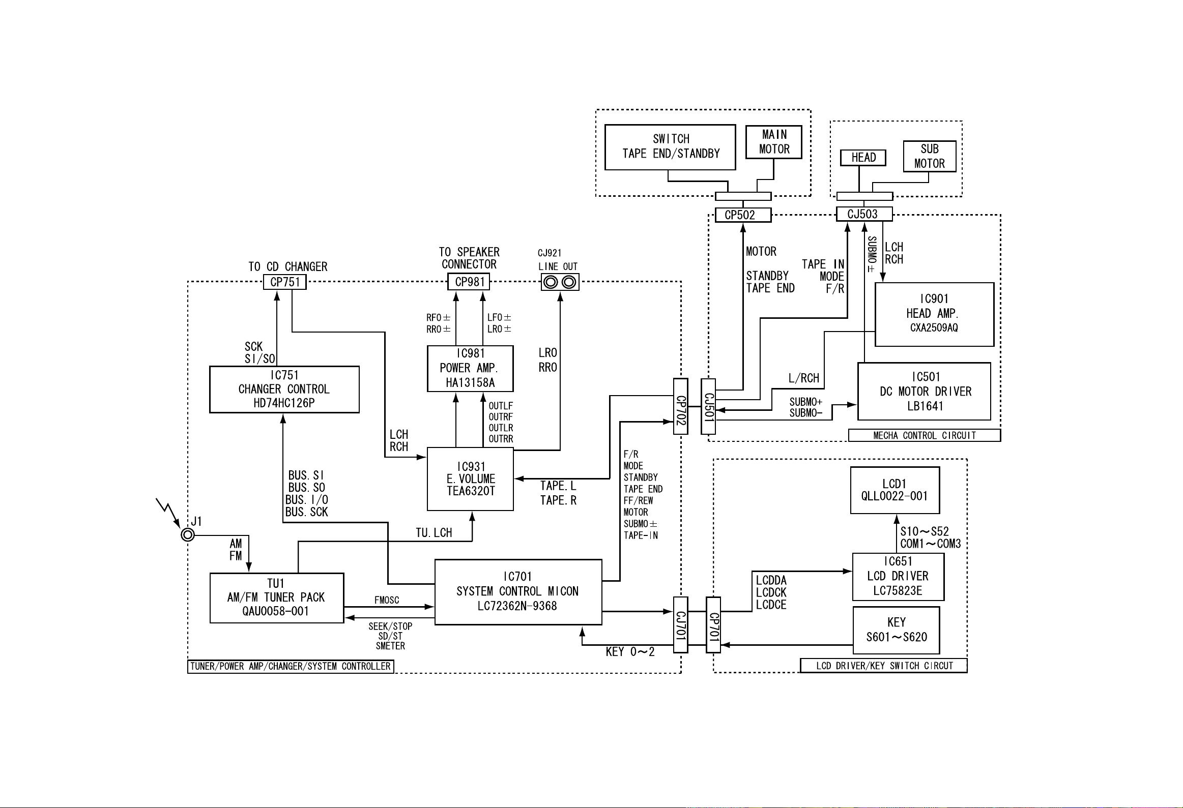
Block diagram
6
5
KS-FX230
4
3
2
1
BC
DE
F
G
HA
I
2-1
Page 3
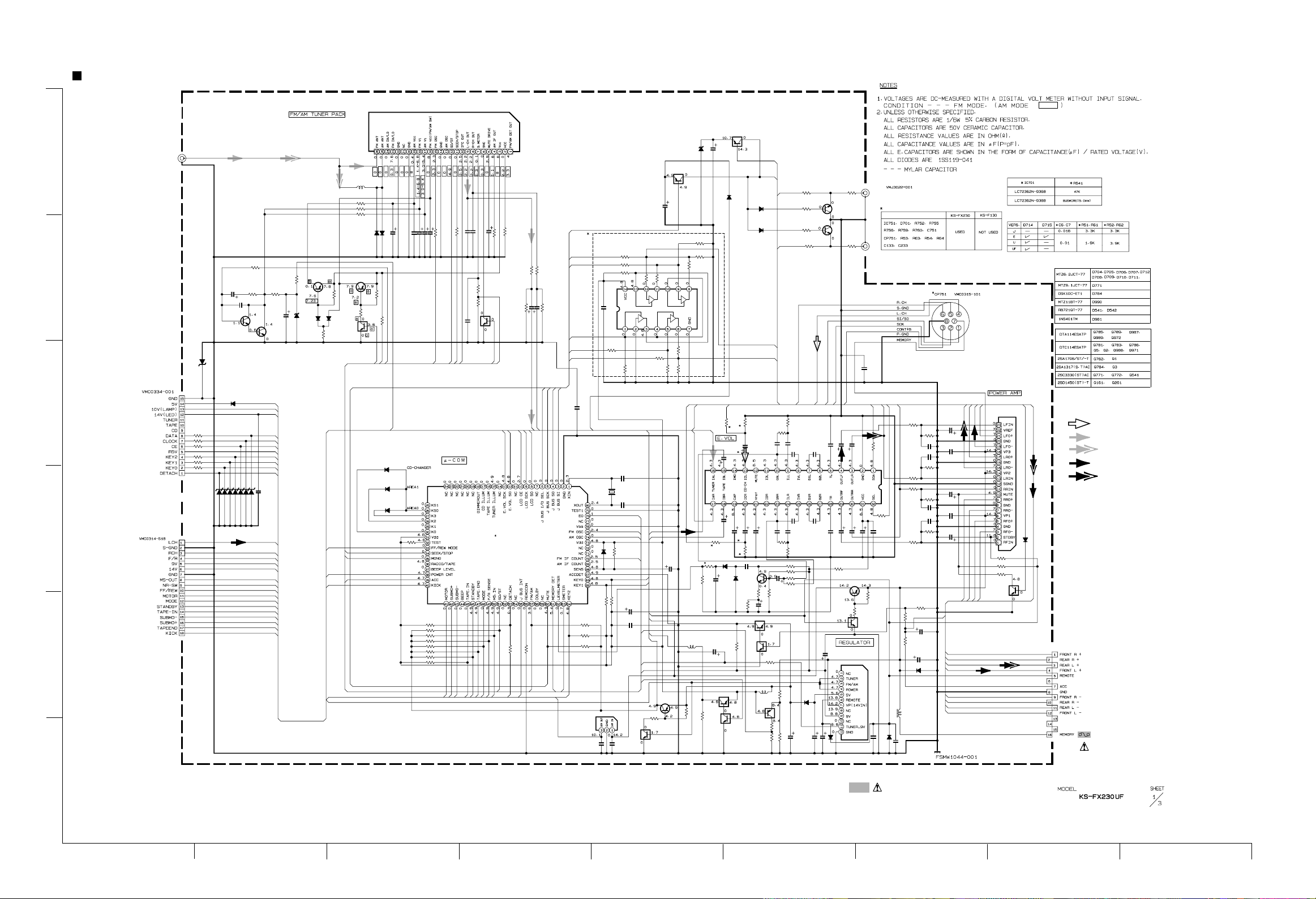
Standard schematic diagrams
Main amp. section
6
5
4
3
2
J1
CJ701
CP702
R774
1.5K
C772
R773
2.2/50
1K
C773
0.001
Q772
Q771
D712
D718
R719
3.3K
3.3K
R718
3.3K
R720
100
R717
100
R716
100
R715
D711
D704
MTZ6.2JCT-77
MTZ6.2JCT-77
LCD.SCK
C708
D705
D706
D707
D708
D709
0.015
MTZ6.2JCT-77
MTZ6.2JCT-77
MTZ6.2JCT-77
MTZ6.2JCT-77
MTZ6.2JCT-77
TAPE.14V
TAPEEND
LCD.SO
LCD.CE
KEY2
KEY1
KEY0
DETACH
TAPE.L
TAPE.R
MS.OUT
DOLBY
FF/REW
MOTOR
MODE
STDBY
TAPEIN
SUBMOSUBMO+
KICK
R771
R772
10K
C771
220/10
5V
10V
14V
R5V
F/R
9V
1K
1K
10K
47K
R764
C702
22P
C701
27P
VCX5026-001
EO
FM.OSC
AM.OSC
47K
R726
IF.C
KEY0
KEY1
C703
100/6.3
C704
0.22
KS-FX230
D990
Q972
C972
220/16
R756
100
10K
R759
R760
HD74HC126P
IC751
100330K
R751
R755
1K
47K
R753
R754
CD.RCH
TAPE.L
TAPE.R
C705
10/16
TAPE.14V
MEM.DET
R5V
5V
TUNER_9V
9V
Q783
14V
Q784
R786
R785
1K
ACC
Q989
C988
47/16
R757
47K
R758
47K
100
14V
CD.LCH
TU.LCH
TU.RCH
L782
47K
C132
C232
1/50
R63
20K
R541
D541
R545
C543
56K
0.47/50
47uH
C785
33/10
Q785
R790
2.7K
Q786
1/50
47/16
C934
ACC
MUTE
SCK
C150
1/50
C250
R164
100
R264
100
14V
1/50
1/50
C260
10
Q782
IC781
BA3918-V1
CJ921
C709
0.047
IC981
R151
RRO
LRO
SDA
SCL
1/50
3.3K
R721
C160
R722
3.3K
C932
0.01
C931
100/10
47K
R783
1K
R784
Q781
0.01
D785
C985
L981
C707
0.01
27K
470P
C162
R161
27K
R261
27K
470P
R251
27K
R988
10K
R989
100
R987
C981
2200/16
D981
1N5401TM
QQR0528-001
2.4K
C984
10/16
R152
82K
C152
470P
R162
82K
R262
82K
C262
C252
470P
R252
82K
LRO+
C986
10/16
C983
0.01
C971
4.7/25
C982
0.01
C951
4.7/25
RRO-
ACC
RFO+
RRO+
LRO+
LFO+
RFORROLROLFO-
HA13158
LRO-
LFO-
LFO+
MUTE
CD SIGNAL
FM/TUNER SIGNAL
AM SIGNAL
TAPE PB/MAIN SIGNAL (Front)
TAPE PB/MAIN SIGNAL (Rear)
D974
4.7K
R951
47K
R971
R972
Q971
470
RFO+
RRO+
RFO-
QNZ0002-001
CP981
R163
LRO
R131
22K
C134
TEA6320T
C234
R231
22K
C541
1/50
R542
22K
R795
R796
RRO
0.0082
0.0082
R543
R546
R133
47K
820
R165
2.2K
Q161
R265
2.2K
Q261
R263
820
SI/SO
CD.RCH
CD.LCH
R132
C138
0.0056
C137
0.15
C135
0.22
0.033
C136
C236
0.033
0.22
C237
0.15
C235
R232
R233
150K
10K
C783
2.2k 2.2k
12K
180K
150K
2200/6.3
C238
0.0056
R931
C784
220/10
D781
C781
C987
D784
10/16
10/16
D710
D161
D261
SCK
SI/SO
R54
20K
R53
7.5K
C133
1/50
IC931
1/50
C233
C933
100/10
R64
7.5K
C542
0.047
Q541
D542
100
R547
1K
R544
22/16
C544
Q987
10K
Q988
R990
6.8
R787
L781
47uH
Q789
R788
100K470K
R789
KS-FX230
QAU0058-001
TU1
L1
4.7uH
R1
10
1K
R2
1K
R3
D1
D2
R6
2.2K
FF/REW
PCNT5V
KICK
Q1Q3
R4
10K
D791
10K
1K
R5
R787
IFREQ
MONO
ACC
BAND
D701
D714
D715
6.8
TUNER_9V
EO
Q2
4.7K
D792
D771
R17
0.1/50
C6
*
0.01
C11
TAPEIN
C7
*
R14
R15
STDBY
1.5M
3.3M
TAPEEND
MODE
8.2K
0.1/50
100K
C8
R10
R11
R61
R51
*
*
1/50
1/50
Q5
S.METER
MONO
IC701
MS.OUT
F/R
SD/ST
C231
C131
R52
*
TU.RCH
TU.LCH
SDA
SCL
LCD.SO
LCD.CE
LCD.SCK
4.7K
47K
R724
R711
BUS.INT
BAND
DETACH
MUTE
0.01
C751
C706
5V
4.7K
3.3K
4.7K
IC790
C793 C792
0.1 0.33
R761
R763
R752
R762
1K
X701
D716
3.3K
3.3K
R714
R713
BUS.INT
BUS.SCK
R62
*
BUS.I/O
BUS.SO
BUS.SI
BUS.SO
BUS.SI
BUS.SCK
MUTE
MEM.DET
10V
S.METER
0.01
R710
R712
R709
KEY2
KIA7810PI
BUS.I/O
100
10/16
0.1/50
10/16
0.022
C1
C3
C2
14V
R727
47K
R725
R708
R702
R703
R704
R705
R706
R707
10K
C5
C4
R8
R9
IFREQ
FM.OSC
SD/ST
47K
47K
47K
47K
47K
47K
47K
47K
SUBMO+
SUBMO-
MOTOR
1
Parts are safety assurance parts.
When replacing those parts make
sure to use the specified one.
BC
DE
F
G
HA
I
2-2
Page 4
KS-FX230
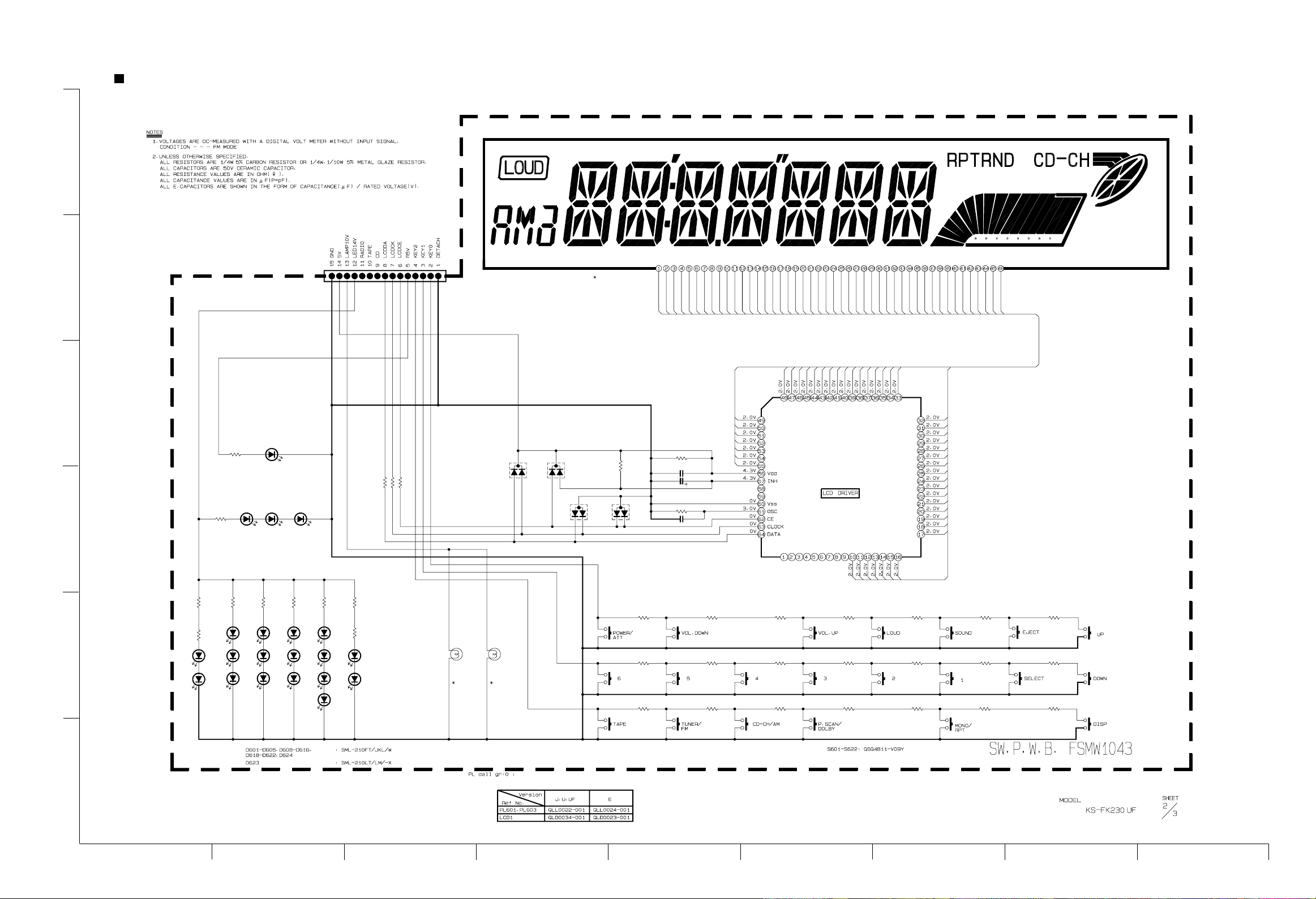
LCD & key switch section
6
D654
MA152WK-TX
MA152WA-TX
D653
LCD1
R653
150k
MA152WA-TX
D652
S10
S11
S12
S13
S14
S15
S16
S17
C651
R651
1.5k
R652
0.01
4.7/6.3
C653
680p
C652
S18
S19
S20
S21
S22
S23
S24
S25
S26
S27
S28
S29
S30
S31
S32
S33
S34
S35
S36
S37
S38
S39
S40
S41
S42
S43
S44
S45
S46
S47
S48
S49
S50
S48
S47
S46
S45
S44
S43
S42
S41
S40
S39
S38
S37
S33
S34
S35
S49
S50
S51
S52
COM1
COM2
COM3
47k
IC651
LC75823E
S36
S32
S31
S30
S29
S28
S27
S26
S25
S24
S23
S22
S21
S20
S19
S18
S17
S10
S11
S12
S13
S14
S15
S16
COM3
COM1
S51
S52
COM2
5
CP701
VMC0335-001
4
D623
R628
R631
820
10K
10K
10K
D602
D603
820
D601
R655
R656
R654
MA152WK-TX
D655
3
820
D618
D619
D620
R636
820
R635
D614
D615
D616
R637
510 510
R640 R638
2
D621
D622
560
820
R634
D612 D611D613
D608
D609D610
D624
R633
R639
510
510
D605 D604
PL601
PL603
R601
270 820
S601 S602
R608 R609 R610
270 330 390
R615 R616 R617
270 330 390
S617 S618 S619 S620
R602
330
S610 S611 S612
S604 S605
R605R603 R604
560390 470
R611
470
R618 R619
470 560
R612 R613
560 820
S613S609
R606
S606
S614
R614 R600
820 1K
S622
S607
S615
R607
R620
1K
1K
S608
S616
S603
1
BC
DE
F
G
HA
I
2-3
Page 5
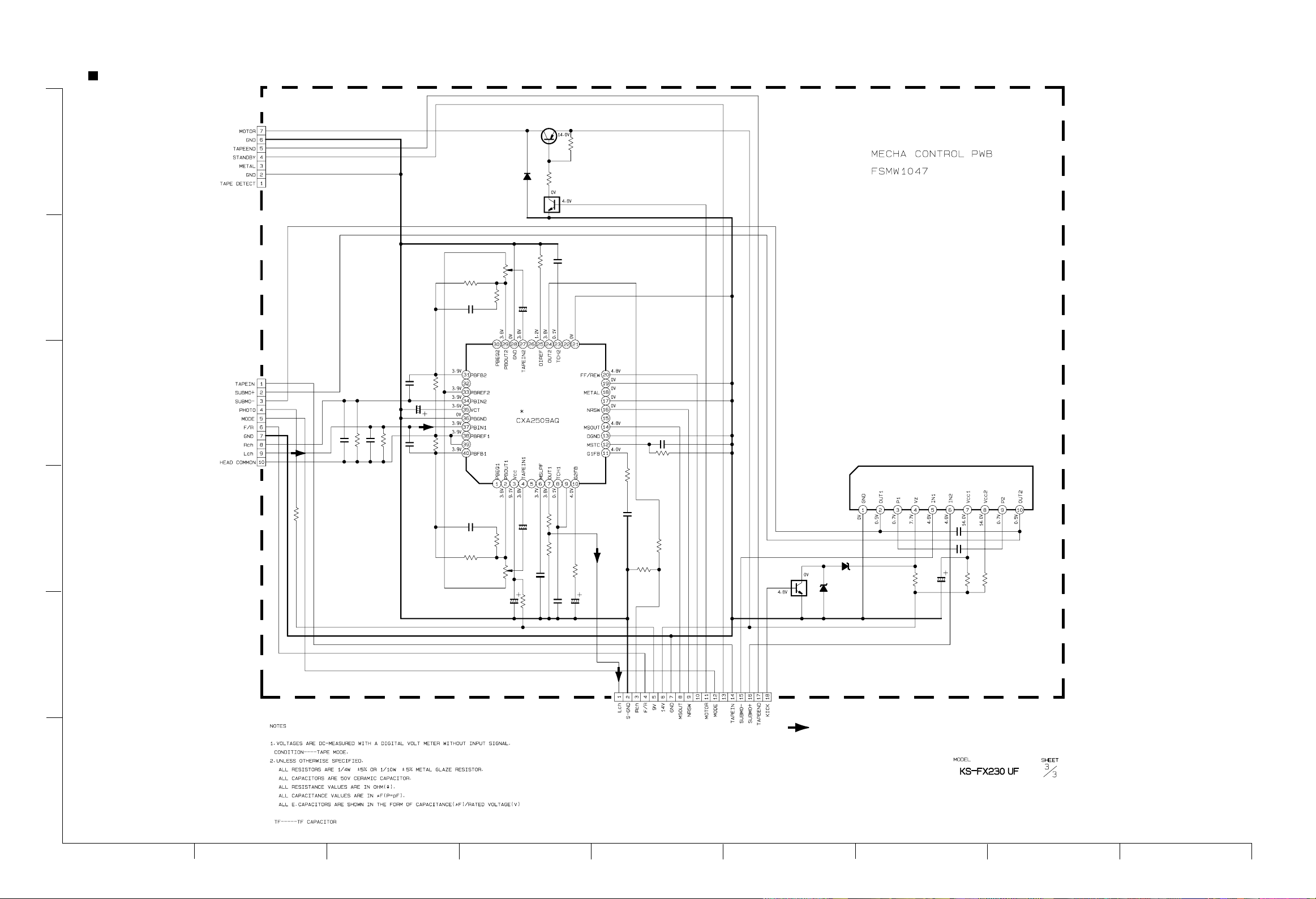
Mecha control section
KS-FX230
KS-FX230
D501
DSK10C
C203
IC901
1/50
Q501
2SB1322( RS)
3.3K
R502
0.1
C204
18K
R907
47K
R501
Q502
DTC114EKA
R903
22K
C905
R904
1.2M
0.1
IC501
LB1641
CP502
6
C202
0.01
VR201
R203
33K
12K
R105 R205
R204
300K
180 180
5
CJ503
4
470P
C101
C201
100K
R201
470P
R101
100K
C205
C906
22/16
C105
100P
100P
5.1K
C103
R901
1/50
100
C902
R108
R109
100P
1.5K
C104
3.3K
C503
10/16
C501
0.01
C502
0.1
R505
33
12
R504
C904
0.01
R208
5.1K
3.9K
R902
0.1
C903
0.47/50
1.5K
R209
Q503
DTC114EKA
D503
MA3075( M)
D502
MA3036( L)
R503
2.2K
R506
3
C102
0.01
R104
300K
R103
VR101
12K
33K
C901
22/16
2
CJ501
TAPE PB/MAIN SIGNAL
1
BC
DE
2-4
F
G
HA
I
Page 6
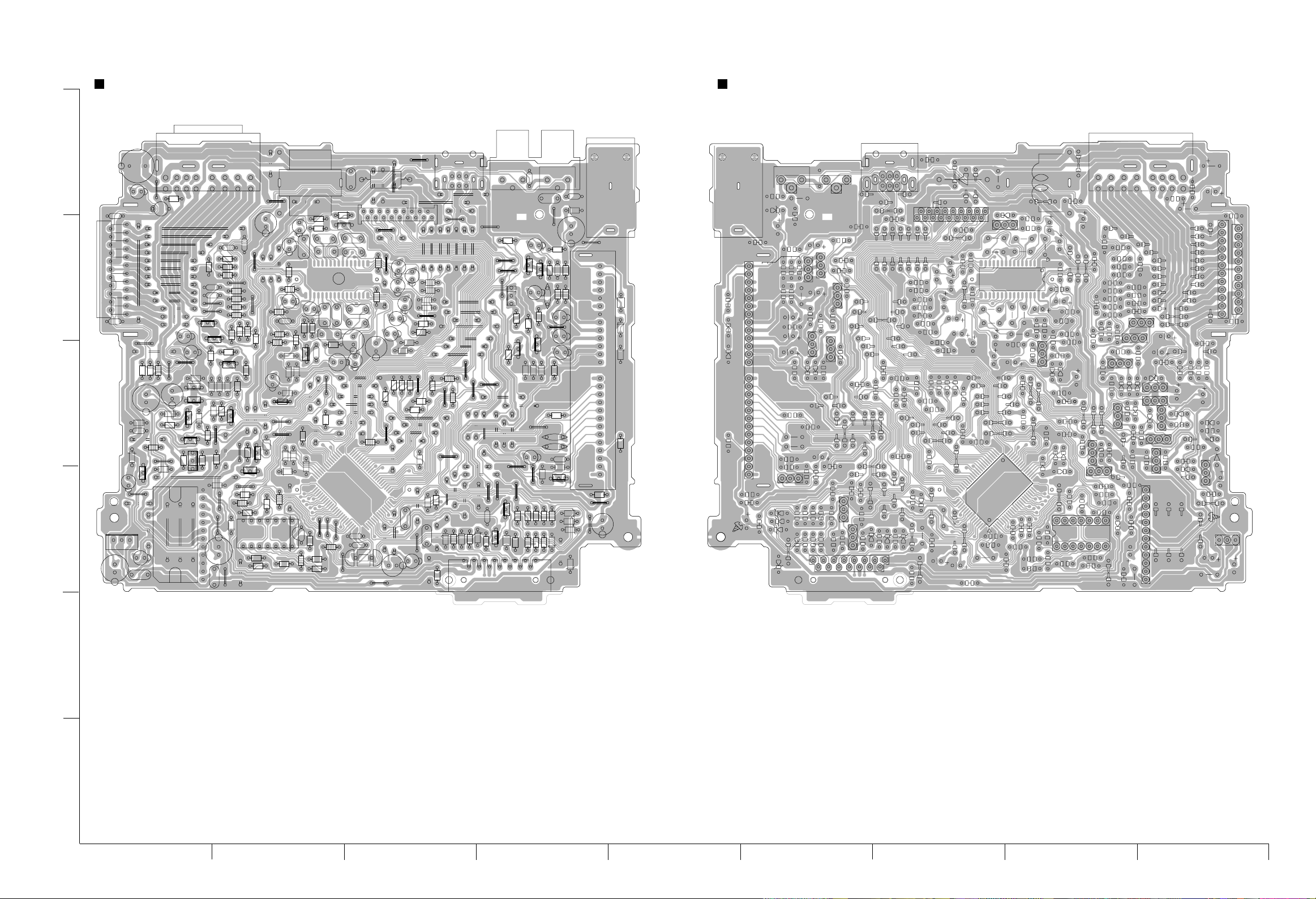
Printed circuit boards
Main board (Forward side) Main board (Reverse side)
KS-FX230
IC790
C983
C987
C982
C783
C972
IC981
B46
B104
B262
C792
R951
C986
B48
D784
C781
C981
B78
B131
R784
D981
C707
B108
R231R232
D713
D541
C260
R132
R131
C234
B94
C751
R727
R759
Q541
R757
C138
D701
R752
L981
B143
D931
Q931
C137
C135
R133
C136
C134
S04
C237
C238
R542
C542
C544
B25
B93
R761
B98
B41
B42
B43
R763
R233
C235
C236
C231
C933
C541
B186
B142
B141
B185
B135
B101
B111
R707
C701
C702
B44
X701
B54
B89
B49
R987
C984
B80
B109
B189
R971
D785
C985
Q781
B261
B251
B241
B232
B218
B217
B216
B215
B187
C152
B188
B144
C971
C951
B36
D990
B39
R989
C988
Q989
Q972
D710
Q783
D973
R786
Q784
Q782
B45
R783
D781
B252
R988
B235
B236
B234
CP981
C262
R251
R262
R252
R261
C162
B2
B33
Q161
R264
Q261
R163
Q971
R165
D974
D161
D261
D789
R788
B37
R785
B145
B35
R795
R796
R755
B40
R754
R764
B52
D718
IC781
C784
B102
B47
C793
R972
Q789
B27
C931
C150
C160
C252
B28
B146
B90B7B91
R931
C932
R263
C543
R762
C250
R546
R543
R541
B56
][
B95
B51
B53
L781
IC751
R756
D714
R545
D715
R547
D542
R751
R721
R722
R544
B100
R760
B30
R162
R152
R151
B31
R161
R164
R265
R789
B96
B97
Q987
R990
Q988
B38
R753
R758
R710
B55
CP751
B88
B147
CP702
B26
B86
B34
C232
B22
B82
B85
C934
B83
B184
C703
R706
R703
R705
B84
C704
C705
C133
R704
C131
B177
C132
C233
B23
R62
R61
B182
B137
B32
B219
B242
B110
B50
B176
B175
B174
B173
R51
R52
R54
R53
R63
R64
B214
R708
B21
R701
B16
R702
B231
B132
B15
R711
R726
D716
B183
B77
C708
D709
R719
B81
R787
B1
B172
B171
B212
B213
B71
B233
B179
B180
B19
B20
B17
R709
B181
B74
B73
B76
B140
B9
B99
B136
B139
C706
D708
R718
D707
R720
Q786
C264
CJ921
C772
R774
B3
B4
Q772
B10
Q1
C1
R4
R6
Q2
R5
D791
R17
B178
B138
B75
B14
C8
B134
B133
B6
B8
B18
R714
R725
Q785
R724
R716
R717
R790
L782
Q771
C709
R713
R715
D792
C164
D771
B13
C771
R771
R772
R773
C773
R2
R3
C2
C3
R1
B5
C4
Q3
C5
R8
R9
C6
C7
C11
R14
Q5
R15
R11
D704
R712
D705
D711
D706
B72
D712
CJ701
J1
B12
L1
D1 D2
R10
TU1
B11
B24
C785
FSMW1044
T04
J1
L1
D1 D2
R10
4
6
R4
R790
CJ701
CE
R5
B
L782
CLOCK
DATA
Q785
C706
R720
Q786
E
78
13
D707
R718
5V
10V[LAMP]
14V[LED]
CP751
1
CP702
TP201
TP101
R63
D709
C132
R54
R53
R64
R62
R701
R702
R703
R711
R726
D716
C708
R787
C705
R51
R52
R708
R709
D708
R719
151
GND
D981
C704
9
R544
R756
R541
IC751
R931
R546
C160
R721
R543
D542
D714
R722
R547
R545
R751
1
C931
C252
R262
R261
R162
R263
R164
R265
C543
Q987
E
L781
B
Q988
R754
R762
R753
R758
L981
C707
D931
18
C135
C136
16
R133
C131
C133
17
C233
C235
R233
C232
R61
R704
R705
C703
C231
R706
C236
C934
C541
R710
R707
C701
C702
X701
Q931
C933
C544
C237
R542
R132
R131
R759
R757
IC931
C542
C260
R231
C150
C138
1
C250
32
R232
C932
B
Q541
E
D541
R727
D713
D701
D715
1
C751
R752
14
R760
BE
C137
C134
C238
C234
R761
R763
CP981
C262
R251
C162
C152
R152
R151
R161
EB
R264
BE
Q261
R972
R163
E
Q971
D161
D974
R789
D261
E
D789
Q789
EB
R788
R785
R990
R795
R796
EB
R988
R755
R764
7
D718
8
C784
C793
R987
R252
Q161
C971
C951
R165
D990
Q989
EB
B
Q972
Q783
D973
B
BE
Q784
E
R783
Q782
IC781
112
C264
RRRL
C709
C771
C772
R771
EB
R3
C2
C1
C3
R1
C4
BE
C5
R8
D792
R9
C6
C7
R15
BE
Q5
R712
R713
D711
R715
DET
CJ921
Q771
D791
C8
R714
Q3
R725
R716
KEY0
R774
EB
Q772
EB
Q1
R6
BE
Q2
R17
R724
BE
R717
R5V
KEY2
KEY1
C164
D771
261
C773
R772
R773
R2
C11
TU1
R14
R11
D704
D705
C785
D706
D712
R786
D781
C984
8
C985
12
D710
R784
R989
R971
Q781
C781
C792
D785
C986
C981
BE
C972
R951
IC981
C987
C982
23
22
2
1
C983
D784
IC790
C783
6
5
4
3
2
1
BC
DE
F
G
HA
I
2-5
Page 7
KS-FX230
KS-FX230
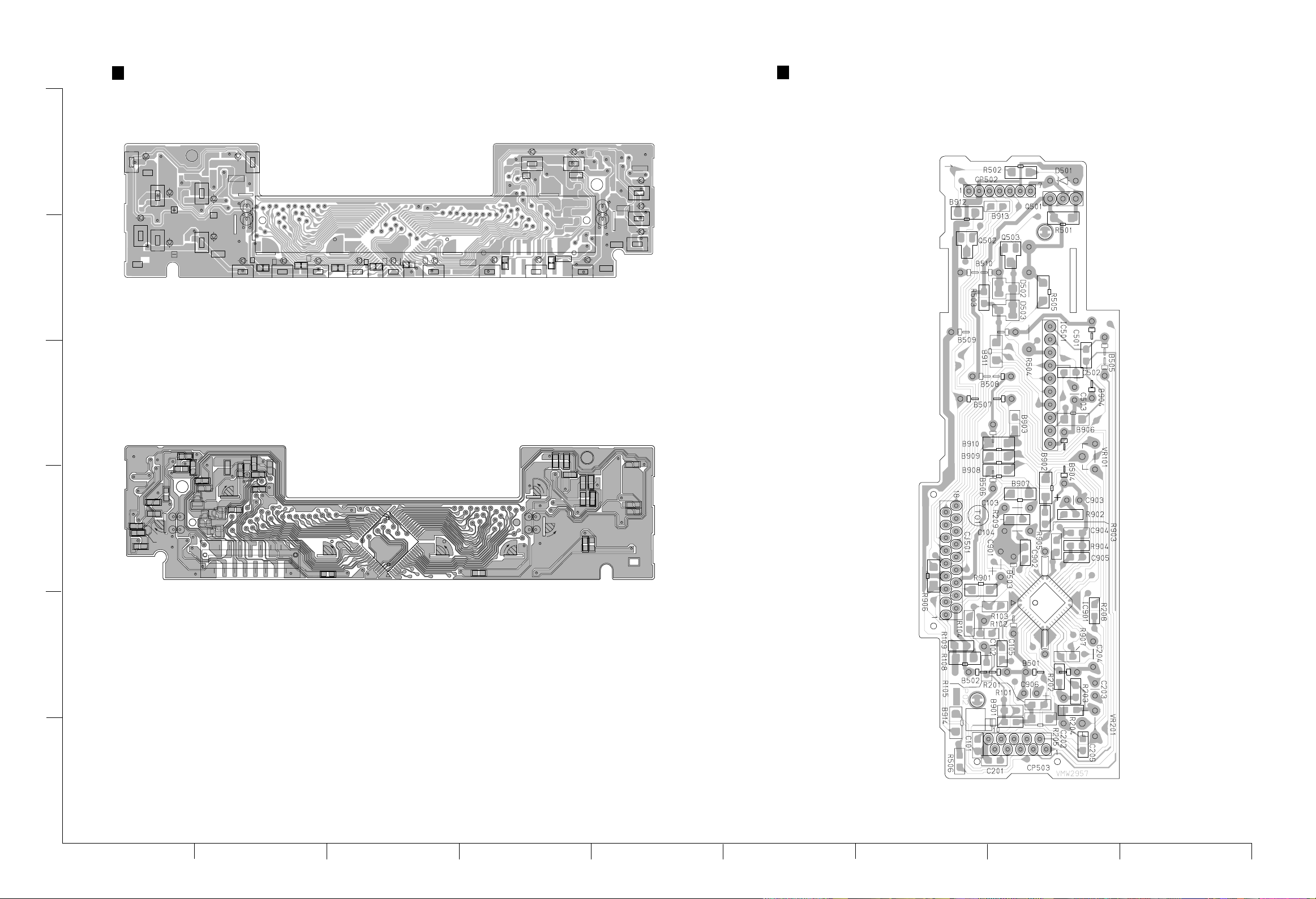
Swich board
Head amplifier board
Forward side
UP
DOWN
D604
PL601
PL602
S614
D605
D608
EJECT
D619
D601
S622
D602
R616
S619
S607
D616
LCD1
D615
S613
1
2
R612
R611
3
D613
D612
D614
S611
S612
R610
S610
R609
4
R608
5
D611
6
CD-CH
S609
D618
S620
MO
SCAN
PL603
TUNER
R615
S618
D603
S617
TAPE
SOUND
D620
S606
D621
LOUD
S605
PL604
D622
S603
DISP
6
D623
I/O
S601
S604
D624
S615
S602
SEL
S608
D609
S01
D610
S616
FSMW1043
5
4
Reverse side
3
2
1
BC
DE
2-6
F
G
HA
I
Page 8

KS-FX230
Safety precaution
!
Burrs formed during molding may be left over on some parts of the chassis. Therefore,
pay attention to such burrs in the case of preforming repair of this system.
1-2
Page 9
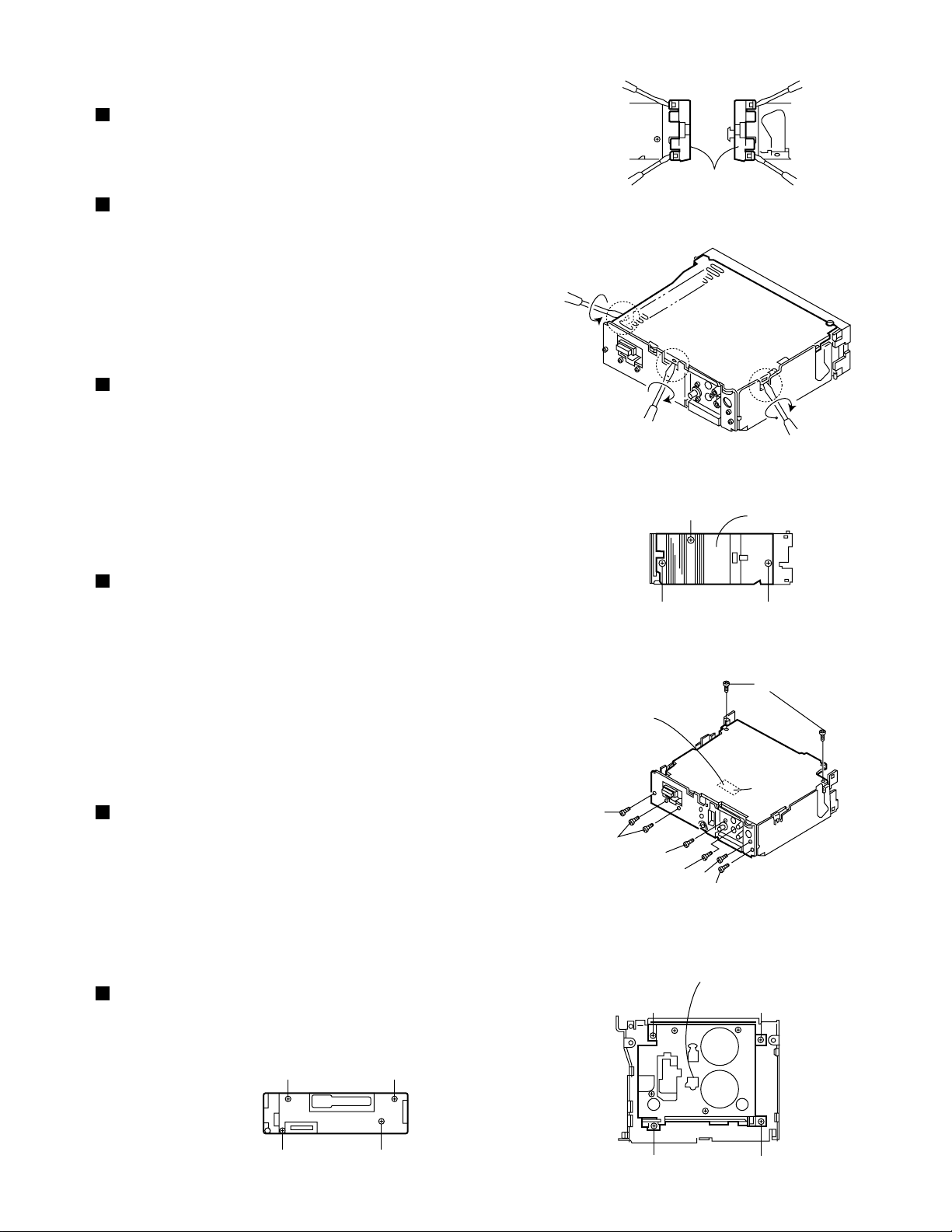
Disassembly method
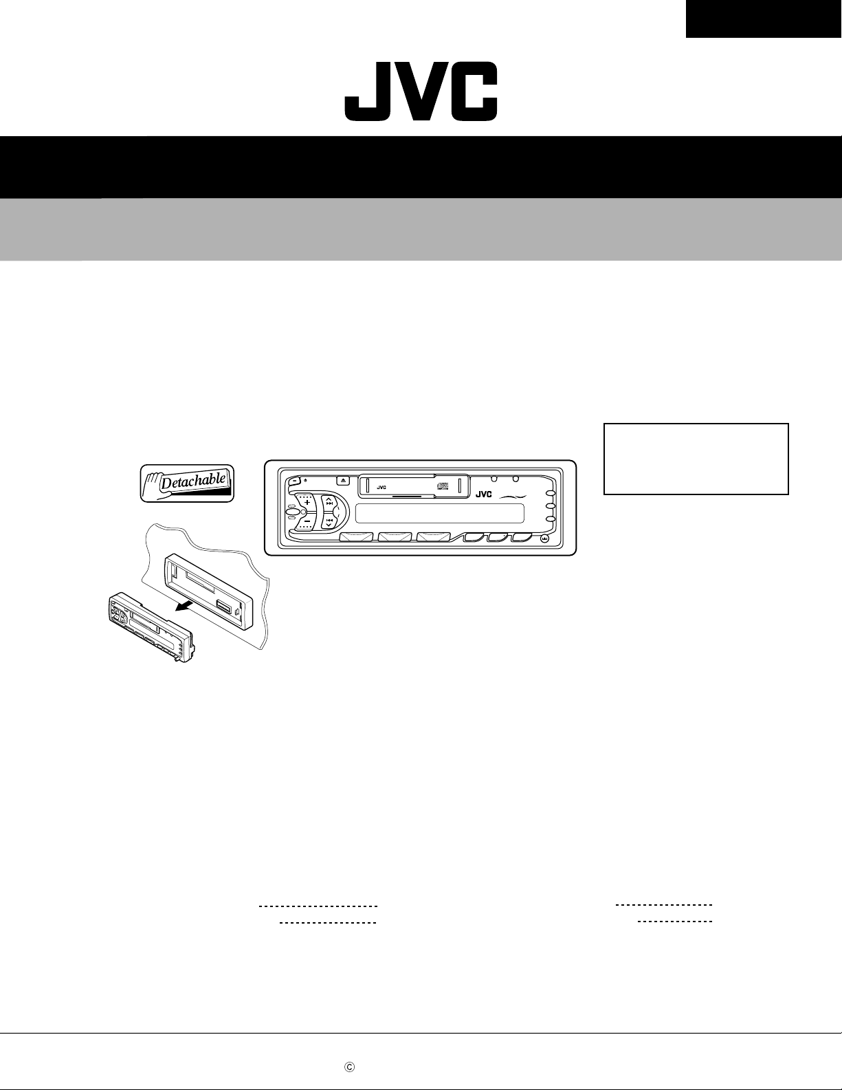
Removing the front chassis (see Fig.1)
1. Disengage the four tabs in the right and left side of
unit and pull the front chassis forward to remove it.
Removing the bottom cover and heat
sink (see Fig.2,3)
1.
Remove one screw A retaining the IC to the heat sink.
2.
Remove two screws B to remove the heat sink.
3.
Turn the upside down, the insert and turn the screwdriver
to remove the bottom cover and protect sheet.
Removing the main board (see Fig.4)
1.
Remove two screws C retaining the rear panel to the
chassis.
2.
Remove two screws D retaining the main board.
KS-FX230
Front chassis
Fig. 1
Bottom cover
Fig. 2
3.
Lift up the main board to remove it. At this time,
remove the connector CP702 connecting the main
board and mechanism assembly.
Removing the rear panel (see Fig.4)
1.
Remove six screws retaining the jacks or the like.
2.
Remove two screws E to the 16-pin jack.
3.
Remove one screw F to remove the line-out jack.
4.
Remove one screw G to remove the antenna jack.
Remove one screw H to remove the changer
controller jack.
Removing the mechanism ass'y (see Fig.5)
1.
Remove four mechanism mounting screws I retaining
the mechanism assembly.
2.
Remove four screws J retaining the cover.
3.
Remove one screw which is the fixation of top cover
and the substrate.
Removing the front panel unit (see Fig.6)
1. Remove four screws K retaining the rear cover.
A
Left side view
BB
Fig. 3
Connection to the mechanism
connector position
C
E
H
F
G
Fig. 4
Mechanism ass'y
JJ
Heat sink
D
Main board
CP702
C
KK
KK
Fig. 6
JJ
Fig. 5
1-3
Page 10

KS-FX230
<< Cassette mechanism section >>
Removing the head relay board (see Fig.1)
1.
Desolder the lead wires of the loading motor at the 2
positions shown (Red and Black).
2.
Desolder the lead wire of the head at the 3 positions
shown (RED, Yellow and Black).
3.
Remove the three screws A securing the head relay
board.
4.
Shift the interlocking section a securing the head
relay board in the direction shown by the arrow to
remove the board.
Removing the load arm ass'y (see Fig.2)
1.
Using tweezers, detach the mylar washer 1 securing
the load arm ass'y and pull out the load arm ass'y.
NOTE : When reassembling, be sure to use a new
mylar washer.
Red
A
Black
Black
Fig. 1
AA
Yellow
a
Red
Head relay board
Catch
2.3.Shift the load arm ass'y counter clockwise.
Remove the load arm ass'y from the catch.
Removing the cassette holder and arm
ass'y (see Fig.3)
1.
Remove the head relay board.
2.
Remove the load arm ass'y.
3.
Apply DC 6V to the lead wire of the loading motor
ass'y and turn the load gear ass'y to the position
shown in Fig. 3.
4.
Remove the screw B securing the cassette holder
and holder arm ass'y.
5.
Shift the cassette holder and holder arm ass'y in the
direction shown by the arrow and remove them from
the interlocking section b of the sub chassis ass'y.
Removing the sub chassis ass'y (see Fig.4)
1.
Remove the head relay board.
Load arm ass'y
Cassette holder
C
1
Fig. 2
B
Holder
b
D
2.
Remove the load arm ass'y.
3.
Remove the cassette holder and holder arm ass'y.
4.
Remove the two screw C and D securing the sub
chassis ass'y.
NOTE : When removing the sub chassis ass'y, the
mode gear may become detached. In this
case, set it back to the original position.
1-4
Sub chassis ass'y
Loading gear ass'y
Loading motor ass'y
Fig. 3
Apply DC 6V
Page 11

Removing the play head (see Fig.4)
1.
Remove the head relay board.
KS-FX230
2.
Remove the load arm ass'y.
3.
Remove the cassette holder and holder arm ass'y.
4.
Remove the sub chassis ass'y.
5.
Disengage the spring holding the play head down.
6.
Remove the two screws E securing the play head.
Removing the pinch roller ass'y (see Fig.5,6)
1.
Remove the head relay board.
2.
Remove the load arm ass'y.
3.
Remove the cassette holder and holder arm ass'y.
4.
Remove the sub chassis ass'y.
5.
Detach the mylar washers c at the two positions
securing the right and left pinch roller ass'y.
Play head
E
Spring
Fig.4
Pinch roller ass'y
c
Fig.5
E
c
NOTE : When reassembling, be sure to use new
mylar washers. Also, make sure that grease
is not adhering to the pinch rollers.
6. Pull out the pinch rollers.
Removing the reel disk ass'y (see Fig.7)
1.
Remove the head relay board.
2.
Remove the load arm ass'y.
3.
Remove the cassette holder and holder arm ass'y.
4.
Remove the sub chassis ass'y.
5.
Detach the mylar washer d from the tip by first
pressing down the reel feather to expose it.
NOTE : When reassembling, be sure to use a new
mylar washer
Pinch roller ass'y
Reel feather
push
Reel disk ass'y
Sub chassis
Fig.6
d
Fig.7
1-5
Page 12

KS-FX230
Removing the head plate (see Fig. 8,9)
1.
Remove the head amp PCB.
2.
Remove the load arm ass'y.
3.
Remove the cassette holder and holder arm ass'y.
4.
Remove the sub chassis ass'y.
5.
Remove the right and left pinch roller ass'y.
6.
From the rear of the head plate, detach the mylar
washer e and the washer pressing the forward/
reverse plate down. (see Fig. 8)
Forward/reverse plate
e
Spring
F
7.
Remove the screw F fixing the metal detection lever
and removal spring as shown in Fig. 8.
8.
Remove the head plate.
9.
Pull out the mode gear. (see Fig. 9)
NOTE : When installing the mode gear, set it to the
arrow mark.
Removing the flywheel ass'y (see Fig. 9)
1.
Remove the head relay PCB.
2.
Remove the load arm ass'y.
3.
Remove the cassette holder and holder arm ass'y.
4.
Remove the sub chassis ass'y.
5.
Remove the head plate.
6.
Disengage the main belt from the flywheel ass'y.
(see Fig. 8)
7.
Remove E washers f at the two positions which
secure the capstan shaft away from the surface.
(see Fig. 9)
Metal tape detection lever
Fig.8
Head plate
f
Capstan shaft
Fig.9
Main belt
f
Marking
Mode gear
8.
Pull out the flywheel ass'y from the rear.
Removing the reel disk PCB (see Fig. 10)
1.
Remove the head relay PCB.
2.
Remove the load arm ass'y.
3.
Remove the cassette holder and holder arm ass'y.
4.
Remove the sub chassis ass'y.
5.
Straighten the curved tab g securing the reel disk
PCB. (see Fig. 10)
6.
Remove the two screws G fixing the reel disc PCB.
7.
Remove the reel disk PCB.
1-6
g
G
Reel desk PCB
Fig.10
Page 13

Removing the loading motor ass'y
1.
Remove the head relay ass'y.
2.
Remove the load arm ass'y.
(see Fig. 11)
KS-FX230
Loading motor ass'y
h
H
Worm gear
3.
Remove the Mylar washer h fixing the worm gear.
(see Fig.11)
NOTE : When reassembling, be sure to use a new
mylar washer.
4.5.Remove the screw H fixing the loading motor ass'y.
(see Fig.11)
Remove the two screws I fixing the loading motor
ass'y. (see Fig 11)
(Procedures for reassembling)
1.2.Insert the mode gear into the sub chassis ass'y.
Install the sub chassis ass'y and secure it with the
two screws C and D as shown in Fig.12.
NOTE : The set arm ass'y and the mode gear
should be positioned as shown in Fig.12.
Sub chassis ass'y
C
Mode gear
Motor bracket
I
Fig.11
Sub chassis ass'y
D
Set arm ass'y
3. Attach the cassette holder as shown in Fig.13. In this
case, first pass the tab of the section i through the
mechanism j, then attach the cassette holder in the
direction shown by the arrow.
Fig.12
Cassette holder
i
j
Fig.13
1-7
Page 14

KS-FX230
4. Set the catch to the holder arm ass'y as shown in
Fig.14.
Holder arm ass'y
5.
While attaching the holder arm ass'y to the cassette
holder, insert the shaft of the holder arm ass'y into
the interlocking section k of the sub chassis ass'y as
shown in Fig.15.
6.
Install the spring attached to the folder arm ass'y
shaft over the set arm ass'y as shown in Fig.16.
7.
After the holder arm ass'y is installed, secure it with
the screw B. (see Fig.15)
Holder arm ass'y
Spring
Catch
Cassette holder
Fig.14
Holder arm ass'y
B
k
Fig. 16
After the installation, apply DC 6V to the lead wires
8.
of the loading motor ass'y to locate the load gear
ass'y as shown in Fig.17.
Install the load arm ass'y.
9.
10.
Install the head relay PCB.
NOTE : Install it so that the slide switch lever of the
head relay PCB is set in the PCB stay hook
of the sub chassis ass'y. (see Fig.18)
11.
Solder the loading motor and head lead wires to the
head relay PCB, respectively. (see Fig.19)
Head PCB
Set arm ass'y
Refer to Fig.16
Fig.15
Loading motor
Apply DC 6V
Fig. 17
Slide switch
1-8
Fig.19
PCB stay
Fig.18
Page 15

Adjustment method
KS-FX230
Equipment and measuring instruments
used for adujustment
Electoronic voltmeter
Audio frequency osillator
(range ; 50 20kHz and outp ut 0 dB with impedance of
660 )
Attenuator (impedance;600 )
Frequency counter
AM Standard signal generator
FM Standard signal generator
Wow flutter mater
Torqu testing cassette gauge
CTG N (mechanical adjusting)
TW 2111A (FWD play)
TW 2121A (REV play)
Standard tape
VT712 or VTT712 (tape speed,wow & flutter adj.)
VT724 or VTT724 (reference level)
VT738 or VTT736 (playback frequency response)
VT721 or VTT721 (output level)
VT703 or VTT703 (azimuth) (10kHz part only)
Preset Memory Initialization
For ver.U
Condition for measurement
Power Spupply DC14.4V
(Reduced voltage ; 10.5V)
Load 4
(4-speakers connection)
BASS / TRE,FADER Indication 0
Main volume Position with an output level
of 2V during VT721 playback
Tuner section
FM ; 400Hz,22.5kHz deviation (MONO)
FM STEREO ; 1kHz,6.5kHz deviation,
pilotsignal 7.5kHz,66dB V
AM ; 400Hz,30% modulation,74dB V
Output impedznce ; 50
Dummy antenna
SSG Level
66dB
FM SSG 50
SSG Level
74dB
AM SSG 50
Coaxial Cable
10
4.5
60
FM DUMMY ANTENNA
Coaxial Cable
15pF
30
60pF
AM DUMMY ANTENNA
Plug to fit
antenna jack
Input Level
60dB
Plug to fit
antenna jack
Metal shield
must be attached to plug
Band
FM(MHz)
AM(kHz)
M1
87.5
531
Preset Memory
M2
M3
89.9
97.9
603
999
M4
105.9
1404
M5
108.0
1602
M6
87.5
531
Manual Tuning Up/Down Frequency
FM: 50kHz
AM: 9kHz
1-9
Page 16

KS-FX230
< Information for using a Car Stereo service jig (for adjustment and checking) >
For 1995 and 1996,we're advancing eff orts to make our extension cords common f or all Car Stereo products .
Please use this type of extension cord as follows.
As a U shape type top cover is emplo yed,this type of extension cord is needed to check operation of the
mechanism assembly after disassembly.
Extension cords
EXT KSRT002 18P (18 pin extension cord)
For connection between mechanism assembly and main
PCB assembly.
Check for mechanism-driving section such as motor , etc.
Disassembly method (Refer to method to remove main parts)
1.
Remove the bottom cover.
2.
Remove the front panel assembly.
3.
Remove the top cover. (Remove the screws at each side of heat sink and rear panel.)
4.
Install the front panel (whose assembly was removed in step 2) to the main unit.
5.
Confirm that current is being carried by connecting an extension cord jig.
Connection diagram
Extension cord
Mechanism assembly
1-10
KS-FX230/KS-F130
Main board assembly
Front panel assembly
Available to connect to the CN701 connector
when installing the front panel.
Page 17

KS-FX230
Item
1.
Head
azimuth
adjustment
Conditions
Test tape:
SCC-1659
VT703(10kHz)
Adjustment and Confirmation methods
Head height adjustment
Adjust the azimuth directly. When you
adjust the height using a mirror tape,
remove the cassette housing from the
mechanism chassis. After installing the
cassette housing, perform the azimuth
adjustment.
Load the SCC-1659 mirror tape. Adjust with
1.
height adjustment screw A and azimuth
adjustment screw B so that line A of the
mirror tape runs in the center between Lch
and Rch in the reverse play mode.
After switching from REV to FWD then to
2.
REV, check that the head position set in
procedure 1 is not changed. (If the position
has shifted, adjust again and check.)
Adjust with azimuth adjustment screw B so
3.
that line B of the mirror tape runs in the
center between Lch and Rch in the forward
play mode.
Head azimuth adjustment
Load VTT724 (VT724) (1kHz) and play it
1.
back in the reverse play mode. Set the Rch
output level to max.
Load VTT703 (VT703) (10kHz) and play it
2.
back in the forward play mode. Adjust the
Rch and Lch output levels to max, with
azimuth adjustment screw B. In this case,
the phase difference should be within 45 .
Engage the reverse mode and adjust the
3.
output level to max, with azimuth
adjustment screw C.
(The phase difference should be 45 or
more.)
When switching between forward and
4.
reverse modes, the difference between
channels should be within 3dB. (Between
FWD L and R, REV L and R.)
S.Values Adjust
A line
Head shield
The head is at low position
during.
B line
Head shield
The head is at High position
during REV.
Output
level:
Maximum
PBHead
FWD Adj B
REV Adj C
(0 ) (45 )
HEIGHT Adj A
phase
Tape speed
2.
and wow
flutter
confirmation
Play back
3.
frequency
response
confiramation
When VTT721 (VT721) (315Hz) is played
5.
back, the level difference between channels
should be within 1.5dB.
Test tape: VTT712
(3kHz)
Test tape: VTT724
(1kHz)
VTT739
(63Hz / 1kHz / 10kHz)
The tuner section is of an adjustment-freedesign. In case the tuner is in trouble, replace the tuner pack.
Check to see if the reading of the F, counter /
1.
wow flutter meter is within 3015 3045(FWD
/ REV), and less than 0.35% (JIS RMS).
In case of out of specification, adjust the
2.
motor with a built-in volume resistor.
Play test tape VTT724, and set the volume
1.
position at 2V.
Play test tape VTT739 and confirm.
2.
1kHz / 10kHz: -1 3dB,
1kHz / 63Hz: 0 3dB,
When 10kHz is out of specification, it will be
3.
necessary to read adjust the azimuth.
Tape speed:
3015
3045Hz
Wow
flutter: less
than 0.35%
Speaker out
1kHz / 63Hz
: 0 3db
1kHz / 10kHz
: -1 3db
Built-in volume
resistor
1-11
Page 18

KS-FX230
Descrption of major ICs
TEA6320T-X (IC931) : E.volume
1.Pin layout
2.Block diagram
10 8 9 7 6
5
12
SDA
1
GND
2
OUTLR
OUTLF
MUTE
TL
B2L
B1L
IVL
ILL
QSL
IDL
ICL
IMD
IBL
IAL
3
4
5
6
7
8
9
10
11
12
13
14
15
16
3.Pin functions
Pin
Symbol
No.
SDA
1
SCL
32
VCC
31
OUTRR
30
OUTRF
29
TR
28
B2R
27
B1R
26
IVR
25
ILR
24
QSR
23
IDR
22
Vref
21
ICR
CD-CH
TAPE
TUNER
20
19
18
17
CAP
IBR
IAR
I/O
Serial data input/output.
I/O
MUTE
21
31
2
19
16
15
13
11
14
22
20
18
17
Functions Functions
POWER
SUPPLY
SOURCE
SELECTOR
23 25 24 26 27 28
VOLUME 1
+20 to -31 dB
LOUDNESS
LEFT
VOLUME 1
+20 to -31 dB
LOUDNESS
RIGHT
Pin
No.
17
Symbol
IAR
BASS
LEFT
+15 dB
LOGIC
BASS
RIGHT
+15 dB
I/O
I
Input A right source.
TREBLE
LEFT
+12 dB
TREBLE
RIGHT
+12 dB
FUNCTION
ZERO CROSS
DETECTOR
VOLUME 2
0 to 55 dB
BALANCE
FENDER REAR
VOLUME 2
0 to 55 dB
BALANCE
FENDER FRONT
HC BUS
REC
VOLUME 2
0 to -55dB
BALANCE
FENDER FRONT
VOLUME 2
0 to -55dB
BALANCE
FENDER REAR
3
4
32
1
29
30
2
3
4
5
6
7
8
9
10
11
12
13
14
15
16
GND
OUTLR
OUTLF
TL
B2L
B1L
IVL
ILL
QSL
IDL
MUTE
ICL
IMO
IBL
IAL
Ground.
output left rear.
O
output left front.
O
Treble control capacitor left channel or
I
input from an external equalizer.
Bass control capacitor left channel or
-
output to an external equalizer.
Bass control capacitor left channel.
Input volume 1. left control part.
I
Input loudness. left control part.
I
Output source selector. left channel.
O
Not used
Not used
Input C left source.
I
Not used
Input B left source.
I
Input A left source.
I
18
19
20
21
22
23
24
25
26
27
28
29
30
31
32
IBR
CAP
ICR
Vref
IDR
QSR
ILR
IVR
B1R
B2R
TR
OUTRF
OUTRR
Vcc
SCL
I
Input B right source.
-
Electronic filtering for supply.
I
Input C right source.
-
Reference voltage (0.5Vcc)
-
Not used
O
Output source selector right channel.
I
Input loudness right channel.
I
Input volume 1. right control part.
-
Bass control capacitor right channel
Bass control capacitor right channel or
O
output to an external equalizer.
Treble control capacitor right channel or
I
input from an external equalizer.
O
Output right front.
O
Output right rear.
-
Supply voltage.
I
Serial clock input.
1-12
Page 19

LC75823E(IC651):LCD driver
KS-FX230
1.Pin layout
48 to 33
49
to to
64
1 to 16
3.Pin function
PIN
No.
1 to 9
10 to 52
32
17
Symbol I/O
S10 to S52
2.Block diagram
COM1 COM2 COM3 S52 S51 S1
VDD1
VDD2
INH
OSC
COMMON
DRIVER
CLOCK
GENERATOR
DI CL CE
LATCH & DRIVER
SHIFT REGISTER
ADDRESS
DETECTOR
Functions
-
NOT USED
O
Segment outputs that display data transferred from
VDD VSS
53 to 55
56
57
58
59
60
61
62
63
64
COM1 to COM3
VDD
/INH
VSS
OSC
CE
CL
DI
serial data.
O
The frame frequency (fo) for the common driver output is
(fosc/384)Hz.
-
Power supply
I
Forcibly terns off the display. regardless of internal data.
Serial data can be input. whether this pin is high or low
-
NOT USED
-
-
To GND
I
Oscillator connection (for the common segment alternating
waveform)
I
Serial data transfer
I
pins.connected to a
I
microprocessor.
CE : Chip enable
CL : Sync.clock
DI : Transfer data
1-13
Page 20

KS-FX230
LC72362N-9388 (IC701) : System control
1. Pin layout
80 to 65
1
64
to to
24
25 to 40
2. Pin function
Pin No. Symbol I/O
1
2
3
4
5
6
7
8
9
10
11
12
13
14
15~18
19~22
23~26
27~30
31
32
33~36
37~40
41~43
44
45~48
49~52
53,54
55,56
57~60
61,62
63~66
67
68
69
70
71
72
73
74
75
76
77,78
79
80
PK1/INT1, PK0/INT0
PJ3/DAC3~PJ0/DAC0
PI1/ADI5, PI0/ADI4
PH3/ADI3~PH0/ADI0
XIN
TEST2
PG3/SI0
PG2/SO0
PG1/SCK0
PG0
PF3/SI1
PF2/SO1
PF1/SCK1
PF0
PE3/SI2
PE2/SO2
PE1/SCK2
PE0
PD3~PD0
PC3~PC0
PB3~PB0
PA3~PA0
V DD
PQ0
PP3~PP0
PO3~PO0
PN3~PN1
PN0/BEEP
PM3~PM0
PL3~PL0
PK3, PK2
HOLD
SNS
LCTR
HCTR
EO3
SUBPD
V DD
AMIN
FMIN
V SS
EO2,EO1
TEST1
XOUT
41
Function
I
4.5MHz crystal oscillator connections
LSI test pin.
General-purpose input/output and serial input/output shared ports.
I/O
Output only port.
O
Key source signal output only ports.
O
Key return signal input only port, of which threshold voltage is designed to be
I
low.
Power supply connections.
O
General-purpose input/output port.
O
Output only port.
O
General-purpose output port/BEEP tone shared output pins.
O
I/O
General-purpose input/output ports.
General-purpose input-output/external interrupt shared port.
I/O
O
General-purpose output port/DAC shared output pins.
I
General-purpose output port/ADC shared input pins.
I
PLL control, CLOCK STOP mode control pin.
I
Voltage sense/general-purpose input pin shared port.
Universal counter (frequency, cycle measurement)/general-purpose input
I
shared input port.
Universal counter/general-purpose input shared input port.
I
O
2nd PLL charge pump output pin.
Sub-charge pump output pin.
O
Power supply connections.
O
AM VCO (local oscillator) input pin.
I
FM VCO (local oscillator) input pin.
I
O
Power supply connections.
Main charge pump output pins.
O
LSI test pin.
4.5MHz crystal oscillator connections
O
1-14
Page 21

3.Block diagram
KS-FX230
XIN
XOUT
FMIN
AMIN
SNS
VDD
VSS
HCTR
LCTR
HOLD
TEST1
TEST2
PA0
PA1
PA2
PA3
PB0
PB1
PB2
BP3
PC0
PC1
PC2
PC3
PD0
PD1
PD2
PD3
PE0
SCK2/PE1
PO2/PE2
SI2/PE3
PF0
SCK1/PF1
SO1/PF2
SI1/PF3
V-DET
DIVIDER REFERENCE DIVIDER SELECTOR
1/16, 1/17
SNSFF
1/2
BUS
DRIV.
LATCH
BUS
DRIV.
LATCH
BUS
DRIV.
LATCH
BUS
DRIV.
LATCH
BUS
DRIV.
LATCH
BUS
DRIV.
PROGRAMMABLE DIVIDER
1/114, 1/124
LATCH
UNIVERSAL
COUNTER
(20bits)
RAM
512 4bits
ROM
12K 16bits
ADDRESS DECODER
PROGRAM COUNTER
STACK
ALU
ADDRESS
DECODER
BUS
DRIVER
INSTRUCTION
DECODER
JUDGE
PHASE
DETECTOR
UNLOCK
F/F
PHASE
DETECTOR
LATCH
LATCH
BUS
DRIV.
LATCH
BUS
DRIV.
LATCH
BUS
DRIV.
BEEP
LATCH
BUS
DRIV.
LATCH
BUS
DRIV.
LATCH
BUS
DRIV.
LATCH
BUS
DRIV.
BUS
DRIV.
SUB
C.P.
MPX
INTERRUPT
E01
E02
SUBPD
EO3
PQ0
PP3
PP2
PP1
PP0
PO3
PO2
PO1
PO0
PN3
PN2
PN1
PN0/BEEP
PM3
PM2
PM1
PM0
PL3
PL2
PL1
PL0
PK3
PK2
PK1/INT1
PK0/INT0
PJ3
PJ2
PJ1
PJ0
PI1/ADI5
PI0/ADI4
PF0
SCK1/PF1
SO1/PF2
SI1/PF3
SIO
LATCH
BUS
DRIV.
ADC
MPX
BUS
DRIV.
PH3/ADI3
PH2/ADI2
PH1/ADI1
PH0/ADI0
1-15
Page 22

KS-FX230
HD74HC126P (IC751) : Changer control
1.Pin arrangement 2. Pin function
11C
21A
31Y
42C
52A
62Y
7GND
3. Block diagram
1A
( TOP VIEW )
14
13
12
11
10
Vcc
4C
4A
4Y
3C
9
3A
8
3Y
Input Output
CA
X
LLH
HH H
Y
ZL
1Y
1C
2A
2C
3A
3C
4A
2Y
3Y
4Y
1-16
4C
Page 23

HA13158A (IC981) : Power amp
1. Pin layout
1 ~ 23
2. Block diagram
14 18 6
INVCC
INPUTBUFFER1
IN1
2
STBY
1
PVCC1PVCC2
AMP1
KS-FX230
3
+
4
-
5
IN2
IN3
IN4
11
13
23
10
MUTE
INPUTBUFFER2
INPUTBUFFER3
INPUTBUFFER4
PROTECTOR (ASO
SURGE, TSD)
12 22
AMP2
AMP3
AMP4
TAB
7
+
8
-
9
15
+
16
-
17
19
+
20
-
21
1-17
Page 24

KS-FX230
BA3918-V1 (IC781) : Regulator
1.Block diagram
REGULATOR
NC TUNER
2.Pin functions
Pin
Symbol
No.
1
2
3
4
5
6
7
8
9
10
11
12
NC
TUNER
FM/AM
POWER
5V
REMOTE
VP
NC
9V
NC
TUNER-9V
GND
FM/AM
I/O
GND
+
+
POWER
OIVPC
5V REMOTE VP
+
NC 9V
+
NC TUNER-9V
Functions
Not used
Output selector of AM and ANT.
O
Output selector for AM or FM or both outputs is off.
O
Output selector of COM and AMP. Only VDD output is on at STAND BY.
O
Output level is 5.6v. Output current is 100mA(min). It is voltage supply
for micro computer. Whenever Vcc terminal is connected, output always
keep running
Voltage which is about 1V lower than Vcc unit voltage. Output current is
500mA(min). Voltage supply for Remote Amp.
To be continued to BACK UP and ACC of car.
O
Not used
Output level is 8.7V. Output current is 150mA(min). It can be used for
system common power supply ; tone control, volume control, balance control,
equalize amplifier.
Not used
Output level is 8.7V. Output current is 250mA(min). Voltage supply for
FM Radio Tuner.
To GND
-
1-18
Page 25

CXA2509AQ(IC901):Cassette mecha controler
1.Block diagram and pin configuration
KS-FX230
LB1641 (IC501) : DC motor driver
1. Pin layout
1 2 3 4 5 6 7 8 9
GNDOUT1 P1
VZ IN1 IN2
2. Pin functions
Input Output
IN1 IN2 OUT1 OUT2
0 0 0 0
1 0 1 0
0 1 0 1
1 1 0 0
VCC1
VCC2 P2
10
OUT2
Mode
Brake
CLOCKWISE
COUNTER-CLOCKWISE
Brake
1-19
Page 26

KS-FX230
<<MEMO>>
1-20
Page 27

KS-FX230
KS-FX230
VICTOR COMPANY OF JAPAN, LIMITED
MOBILE ELECTRONICS DIVISION
PERSONAL & MOBILE NETWORK B.U. 10-1,1Chome,Ohwatari-machi,Maebashi-city,Japan
(No.49565)
1-21
Printed in Japan
200007(O)
 Loading...