

Page 1
SERVICE MANUAL
CASSETTE RECEIVER
KS-FX201
KS-FX201
Contents
Safety precaution
Disassembly method
Adjustment method
Description of major ICs
Area Suffix
U ---- Other Areas
1-2
1-3
1-12
1-16
This service manual is printed on 100% recycled paper.
COPYRIGHT 2001 VICTOR COMPANY OF JAPAN, LTD.
No.49589
Jan. 2001
Page 2

KS-FX201
Safety precaution
!
Burrs formed during molding may be left over on some parts of the chassis. Therefore,
pay attention to such burrs in the case of preforming repair of this system.
1-2
Page 3
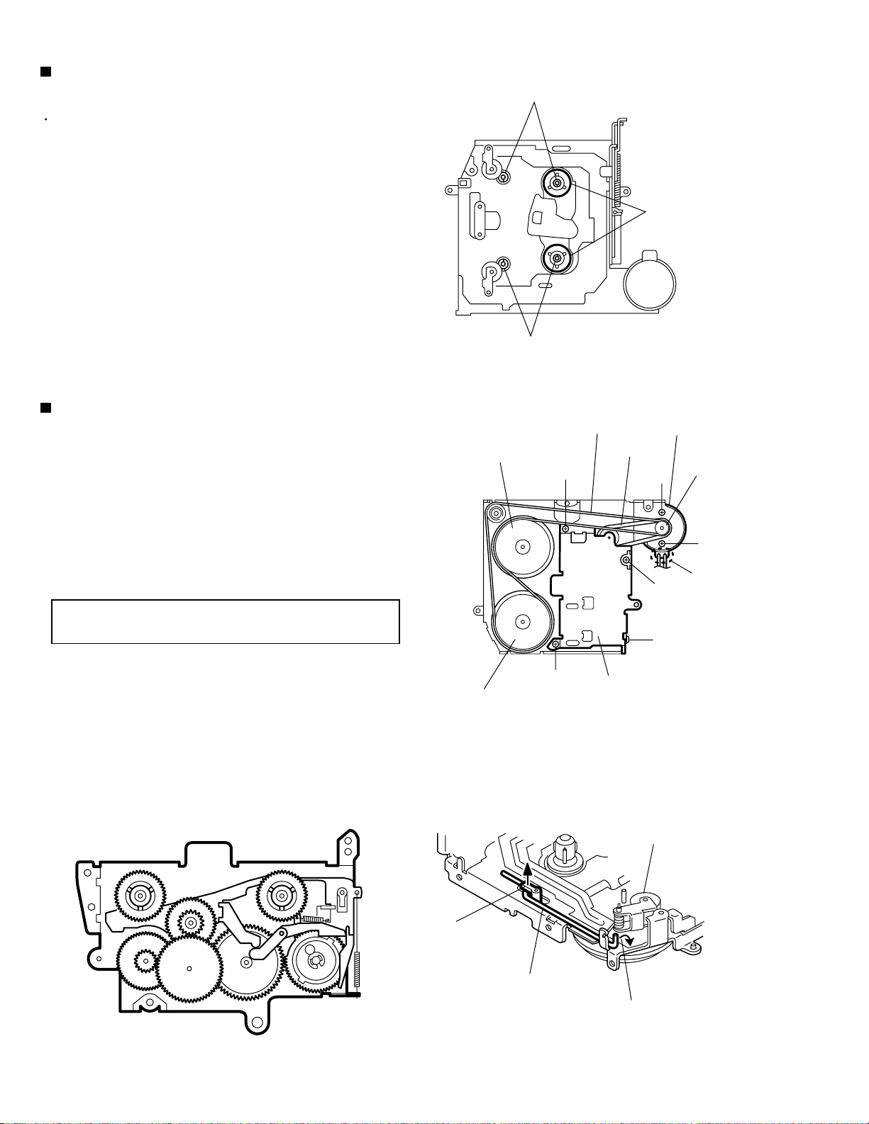
Disassembly Method
KS-FX201
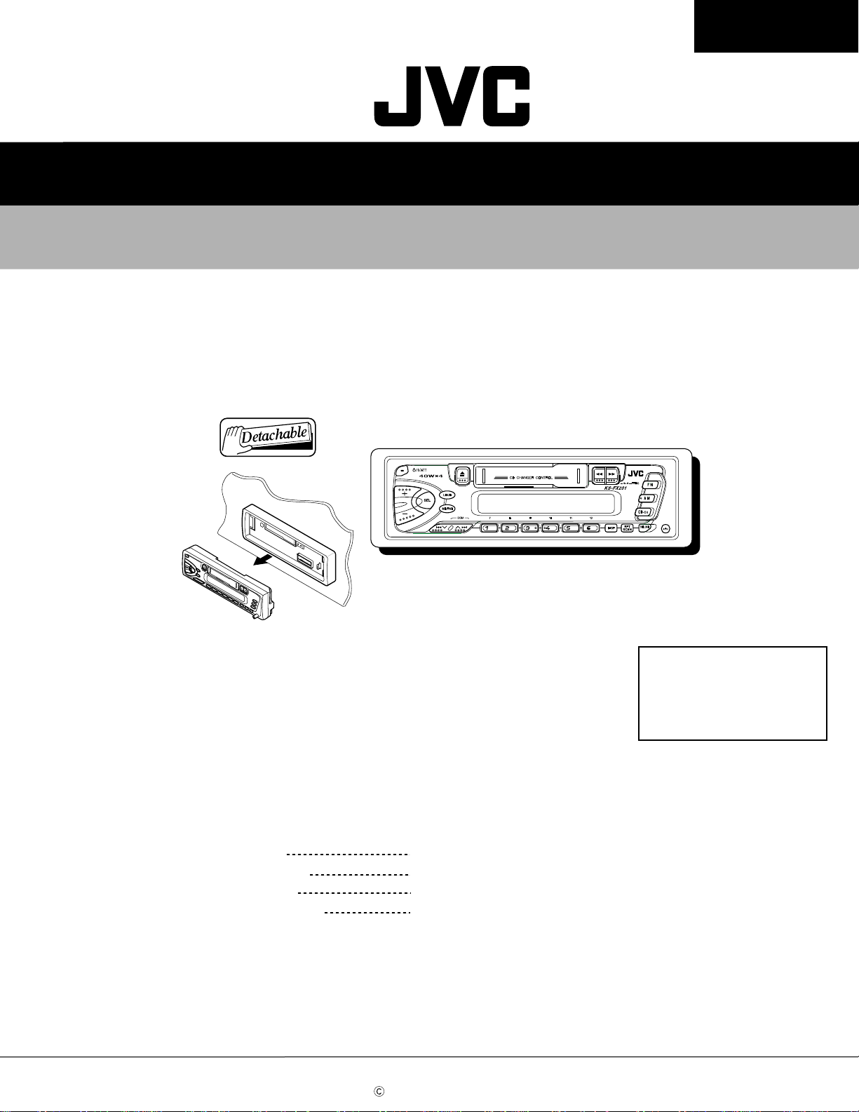
Detaching the Front Panel Unit
( See Fig.1 )
Push the Release button in the direction of arrow to
detach the front panel unit.
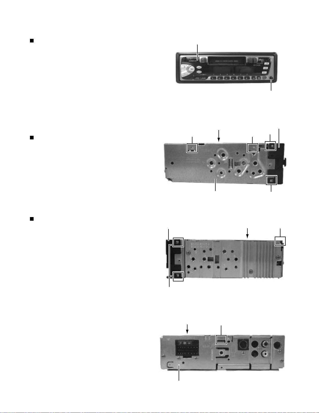
Removing the Front Chassis
( See Fig. 2 and 3 )
Disengage the four tabs ( a ) in the right and left sides of
unit and pull the front chassis forward to remove it.
Front panel unit
Fig. 1
Bottom cover
Push the release button
Front chassis
bc
a
Removing the Bottom Cover
( See Fig. 2 to 4 )
1. Removing the front chassis.
2 . Turn the unit up side down.
3. Insert the four engagements ( b, c, d, e ) to the
screwdriver .
4 . Turn the screwdriver and remove the bottom
cover.
Front chassis
a
Bottom cover
Top chassis
Fig. 2
Fig. 3
e
Bottom cover
a
d
Rear panel
Fig. 4
1-3
Page 4
KS-FX201
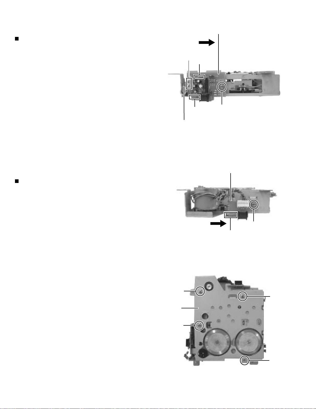
Removing the Heat Sink ( See Fig. 5 )
1. Removing the front chassis.
2. Removing the bottom cover.
3. Remove the three screws ( 1 and 1' ) retaining the
heat sink.
Removing the Main Board Assembly
( See Fig. 5 to 7)
1. Removing the front chassis.
2. Removing the bottom cover.
3. Removing the heat sink.
Attach the heat sink with a screw ( 1' ) on operat-
( )
ing checks.
4. Remove the two screws ( 2 ) retaining the main
board assembly.
5. Remove the six screws ( 3 ) and one screw ( 3' ) retaining
the rear panel.
6. Separate the main board assembly and cassette
mechanism assembly.
7. Take out the main board assembly.
1
Heat sink
1'
Fig. 5
1
2
2
Main board assembly
Fig. 6
3
3
Rear panel
Fig. 7
3'
3
1-4
Page 5
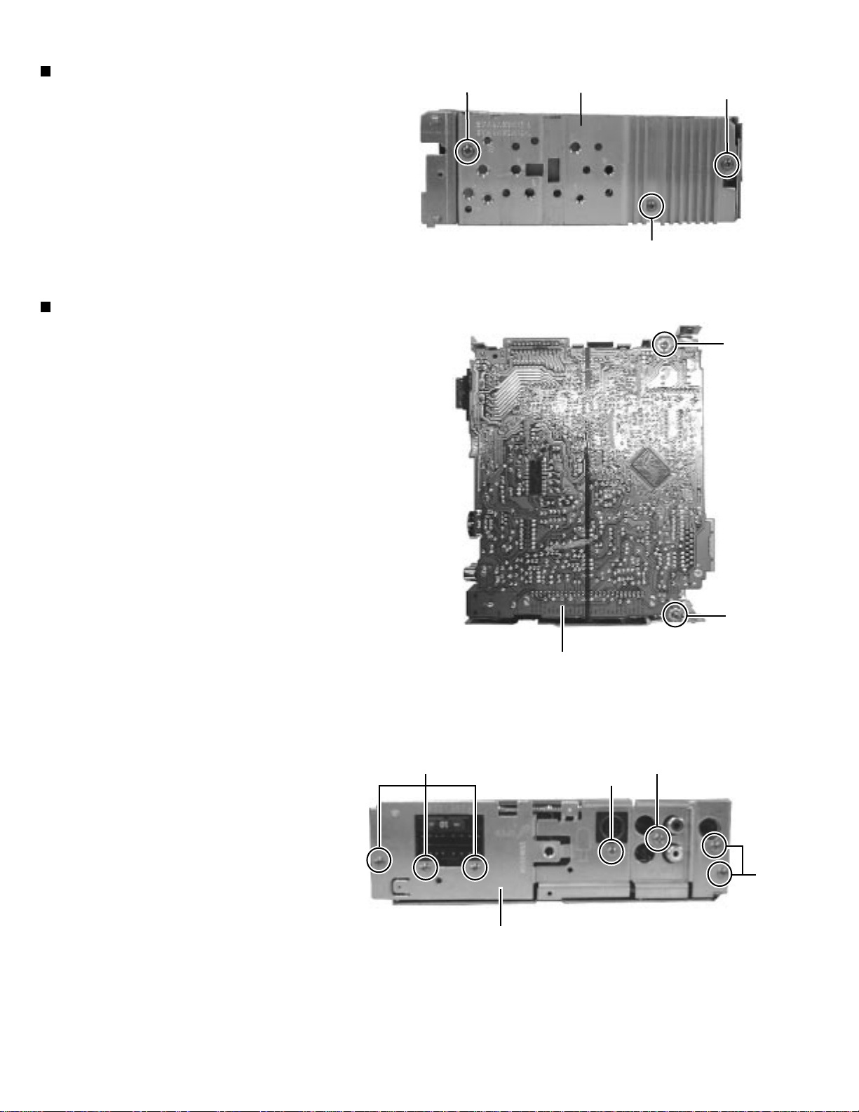
Removing the Cassette Mechanism assembly
( See Fig. 8 )
1. Removing the front chassis.
2. Removing the bottom cover.
3. Removing the heat sink.
4. Removing the main board assembly .
5. Remove the four screws ( 4 ) retaining the cassette
mechanism.
6. Separate the top chassis and cassette mechanism.
Cassette mechanism
4
KS-FX201
4
Front side
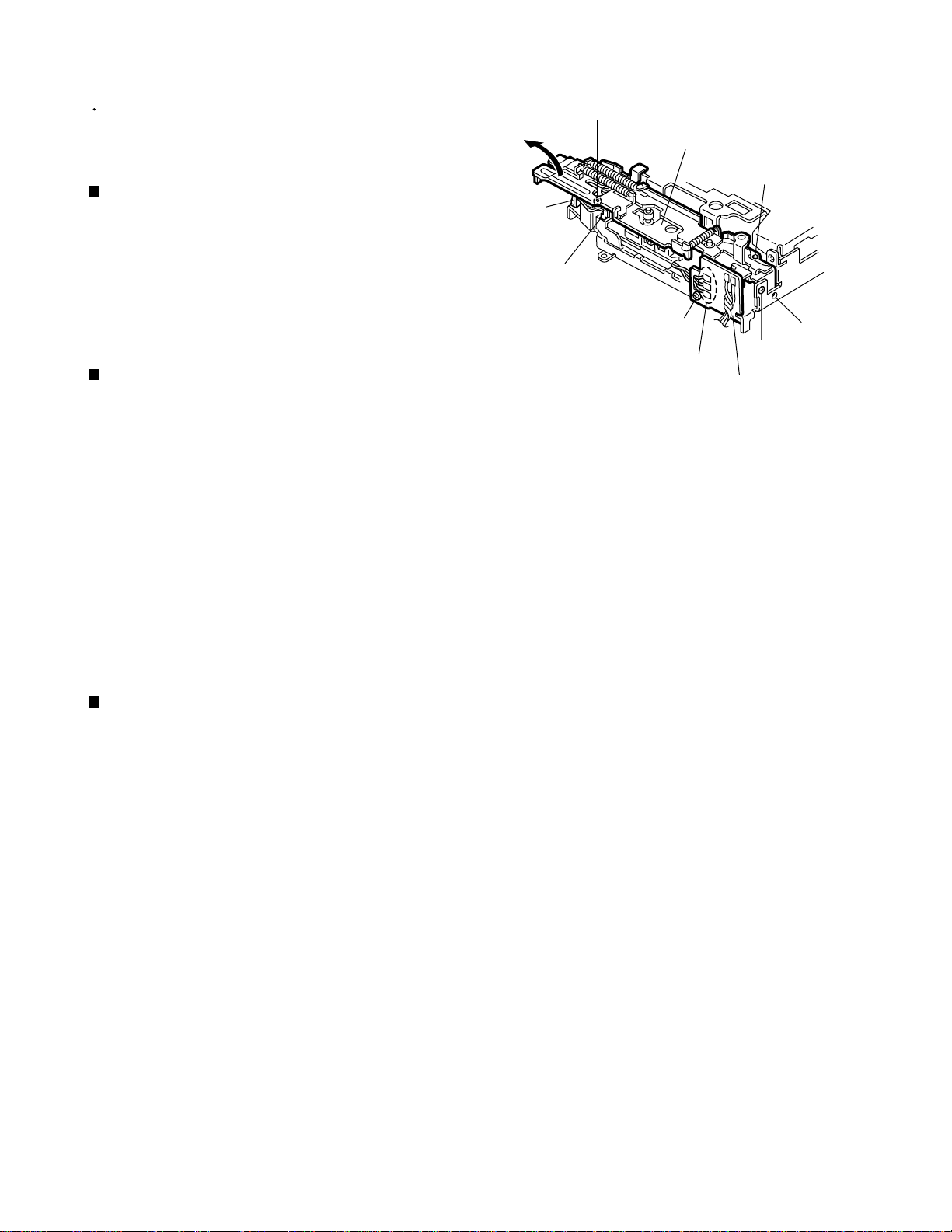
Removing the Operation Switch board
( See Fig. 9 to 11)
1. Detaching the front panel unit.
2. Turn the front panel back side down.
3. Remove the four screws ( 5 ) retaining the front
cover.
4. Open the front cover gradually by disengaging the
three engagements ( g ) while pushing the top of
the front cover in the arrow "A" direction, then
disengage the three engagements ( h ) on the both
sides.
5. Place the front panel unit front side down.
6. Disengage the three engagements ( i ) on the
bottom to separate the front cover from the front
panel.
(Be careful not to lose the button springs.)
h
g
5
5
Front panel
4
Top chassis
Fig. 8
Front cover
Front cover
A
Fig. 9
Fig. 10
4
g
g
5
h
h
5
iii
Operation switch board
Fig. 11
1-5
Page 6
KS-FX201
Head amplifier board
Removing the Head Amplifier Board
( See Fig. 12 )
1. Removing the front chassis.
2. Removing the bottom cover.
3. Removing the heat sink.
4. Removing the main board assembly .
5. Removing the cassette mechanism.
6. Remove the screw ( 6 ) retaining the head amplifier board.
7. Shift the two inter rocking sections ( j ) securing
the head amplifier board in the direction shown by
the arrow "B" to remove the printed circuit board.
8. From the connector CJ901 on the head amplifier
board from connector wire out going to the head
relay board.
Removing the Chassis Assembly
B
CJ901
To head relay board
j
j
6
Fig. 12
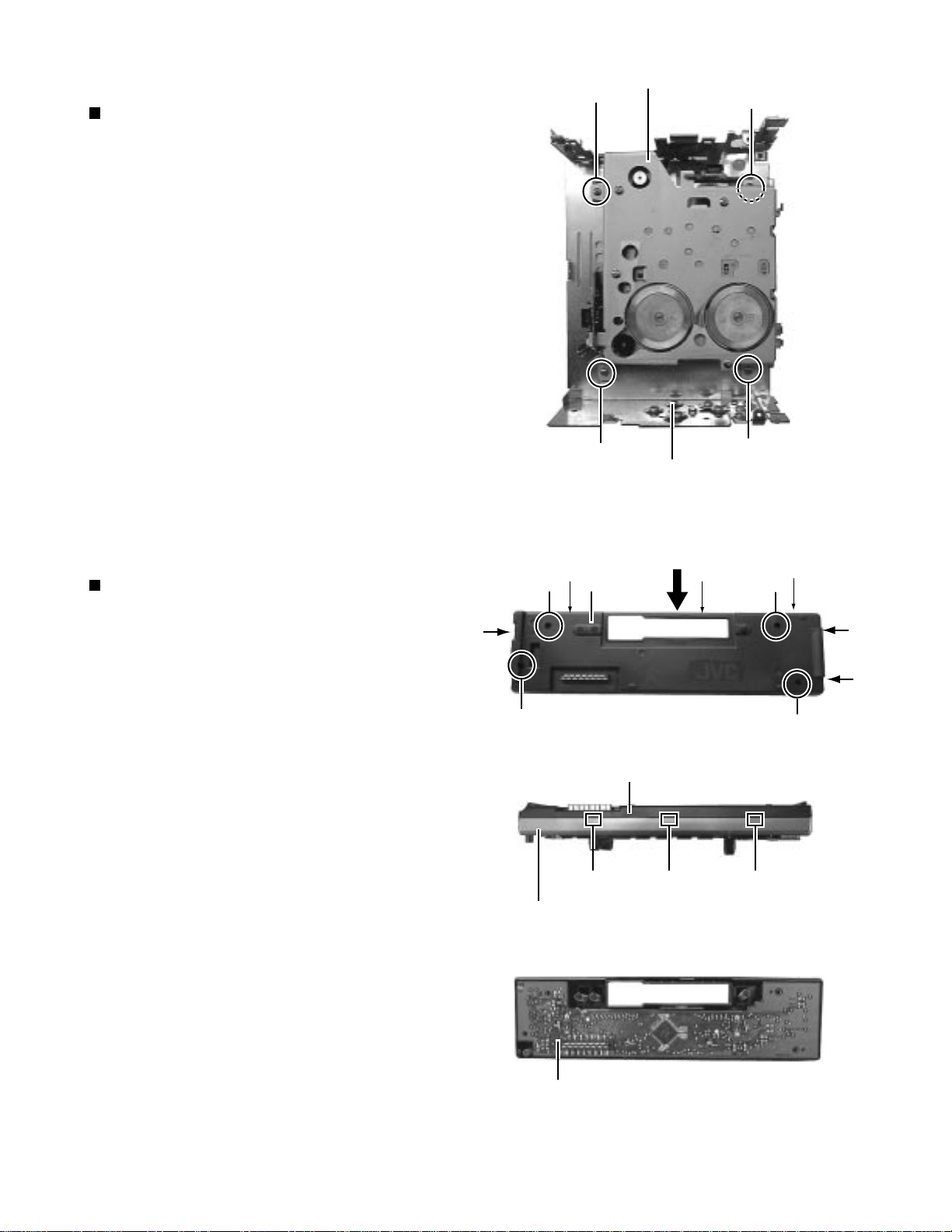
Relay board
( See Fig. 13 and 14 )
1. Removing the front chassis.
2. Removing the bottom cover.
3. Removing the heat sink.
4. Removing the main board assembly .
5. Removing the cassette mechanism.
6. Removing the head amplifier board.
7. Turn the left side to cassette mechanism.
8. Remove the screw ( 7 ) retaining the relay board.
9. Shift the one inter rocking sections ( k ) securing
the relay board in the direction shown by the
arrow "C" to remove the printed circuit board.
10. Turn the back side down, remove the four screws
( 8 ) retaining the chassis assembly.
Chassis assembly
C
k
Fig. 13
8
8
7
8
1-6
8
Fig. 14
Page 7
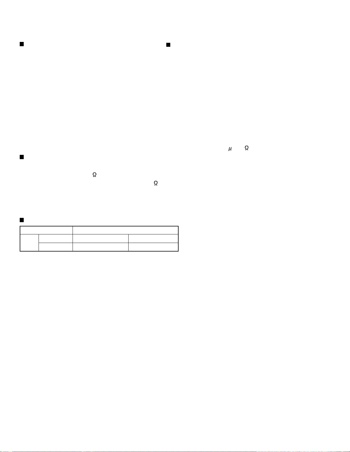
<Cassette mechanism assembly>
KS-FX201
Prior to performing the following procedures, remove
the head amplifier board, the relay board and the
mechanism bracket.
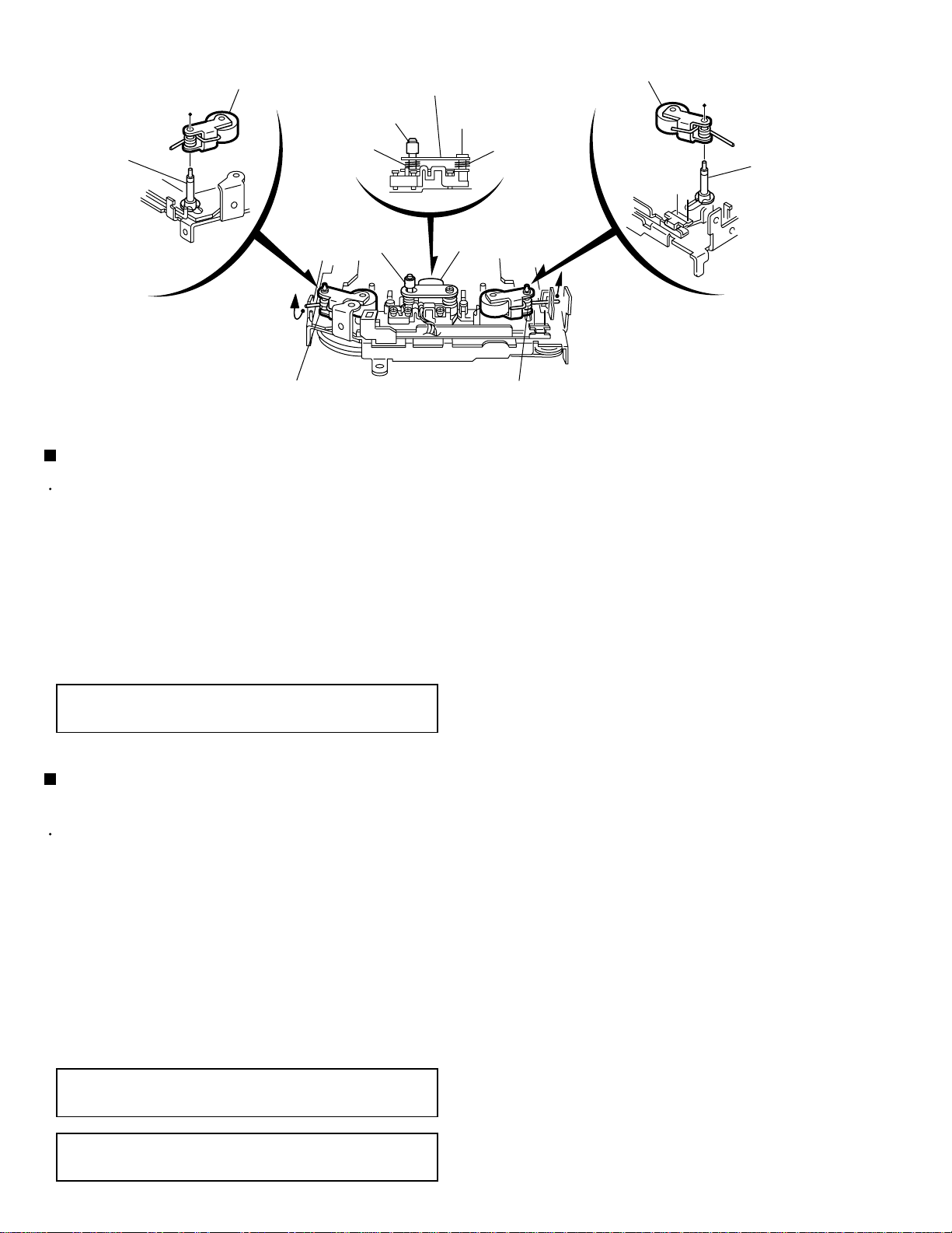
Removing the direction switch board
(See Fig.1)
1.
Unsolder the three wires a on the direction switch
board.
2.
Remove the one screw A attaching the direction
switch board.
Removing the FF / REW lever assembly
(See Fig.1)
1.
Remove the screw B attaching the FF / REW lever
assembly on the back of the cassette mechanism
assembly.
2.
Remove the screw C on the upper side of the FF /
REW lever assembly.
3.
Lift and pull forward the FF / REW lever assembly to
disengage the joints b, c, d and e.
Joint e
Joint d
C
FF / REW lever assembly
A
Solding a
Direction switch board
Fig.1
Joint c
Joint b
B
Reattaching the FF / REW lever assembly
(See Fig.1)
1.
Reattach the FF / REW lever assembly to the joint c
on the back of the chassis.
2.
Reattach the pinch-roller shaft e, the change lever d
and the return link e to the chassis.
1-7
Page 8
KS-FX201
Pinch-roller (R) assembly
A arm spring (b)
Shaft
Remove the P arm spring (r)
from the chassis.
P arm spring (r)
S support plate
C washer
FF roller
Removing the playback head (See Fig.2)
Prior to performing the following procedure, remove
the direction switch board and the FF / REW lever
assembly.
Pinch-roller (F) assembly
D
A arm spring (a)
Shaft
Playback head
Remove the P arm spring (f)
from the chassis.
P arm spring (f)
Fig.2
1.
Remove the screw D attaching the playback head.
2.
Remove the C washer and pull out the FF roller.
3.
Remove the S support plate, the A arm spring (a)
and (b), the playback head.
ATTENTION:
The A arm spring (a) differs from the A
arm spring (b).
Removing the pinch-roller (R) and (F)
assembly (See Fig.2)
Prior to performing the following procedure, remove
the direction switch board and the FF / REW lever
assembly.
1.
Remove the P arm spring (f) in the pinch-roller (F)
assembly from the chassis.
2.
Remove the P arm spring (r) in the pinch-roller (R)
assembly from the chassis.
3.
Draw out the pinch roller (F) and (R) assembly from
the shaft.
ATTENTION:
The P arm spring (f) differs from the P
arm spring (r).
ATTENTION:
The pinch roller (F) assembly differs
from the pinch roller (R) assembly.
1-8
Page 9
KS-FX201
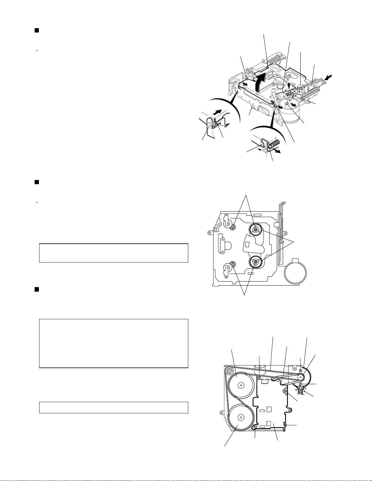
Removing the cassette hanger / cassette
holder (See Fig.3)
Prior to performing the following procedure, remove
the FF / REW lever assembly.
1.
From the rear of the unit, bend the two tabs f
outwards and disengage the two joints g in the
direction of the arrow.
2.
Push the eject lever and remove the cassette holder
from the playback head. Disengage the two joints h
of the cassette hanger / cassette holder and the eject
lever in the direction of the arrow.
3.
Lift the cassette hanger / cassette holder and disengage
the joint i of the return link and the eject lever.
Removing the reel disc assembly
(See Fig.4)
Prior to performing the following procedure, remove
the FF / REW lever assembly and the cassette
hanger / cassette holder.
Joint g
Cassette holder
Return link
Joint i
Cassette hanger
Eject lever
Joint h
Chassis
Joint h
Tab f
Tab f
Joint g
Fig.3
C washer
1.
Remove the C washer and pull out reel disc assembly.
ATTENTION:
Replace with a new C washer when
reattaching.
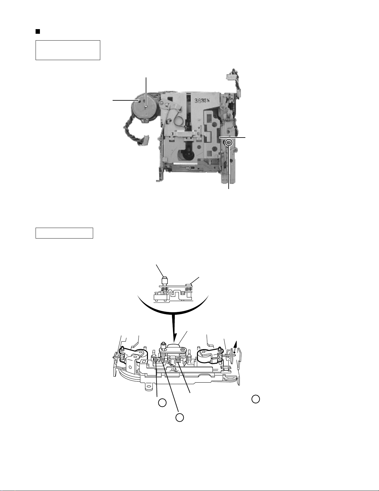
Removing the motor assembly
(See Fig.5)
1.
Unsolder the two wires j on the motor assembly.
ATTENTION:
2.
Turn over the cassette mechanism assembly and
remove the main belt and the sub-belt from the
motor pulley.
ATTENTION:
To replace the sub-belt, remove the
main belt and the sub-belt from the
motor pulley. Then remove the three
screws E and one screw F. Replace
with a new sub-belt while lifting the reel
base assembly slightly.
The main belt can now be removed.
C washer
Flywheel (BF)
Fig.4
Main-belt
E
Reel disc assembly
Motor assembly
Sub-belt
G
E
Motor pulley
G
Solding j
3.
Remove the two screws G attaching the motor
assembly.
Flywheel (BR)
Reel base assembly
E
Fig.5
F
1-9
Page 10
KS-FX201
Removing the Flywheel (BF) and (BR)
assembly (See Fig.4 and 5)
Prior to performing the following procedure, remove
the cassette hanger / cassette holder.
1.
From the upper side of the cassette mechanism
assembly, remove the C washer from each shaft of
the flywheel (BF) and (BR).
2.
Turn over the cassette mechanism assembly and
remove the main belt. Pull out the flywheel (BF) and
(BR) downward respectively.
Removing the reel base assembly
(See Fig.5 and 6)
1.
Raise the part k of the reel base assembly slightly
and remove the selector link (B) on the front side of
the cassette mechanism assembly by turning it as
shown in Fig.10.
C washer
C washer
Flywheel (BF)
Fig.4
Main-belt
E
Reel disc assembly
Motor assembly
Sub-belt
G
Motor pulley
2.
Remove the three screws E and the one screw F
on the underside of the cassette mechanism
assembly.
ATTENTION:
The reel base assembly is not
repairable. Handle with care.
Inside of the reel base assembly
Flywheel (BR)
k
Reel base assembly
E
Fig.5
Pinch-roller (R) assembly
G
Solding j
E
F
1-10
Selector link (B).
Turn the selector link (B).
Fig.6Fig.7
Page 11
Removing the mute switch board
(See Fig.8)
1.
Unsolder the two wires l on the mute switch board on
the back of the cassette mechanism assembly.
2.
Remove the screw H attaching the mute switch
board.
Cassette mechanism assembly
Solding l
Fig.8
H
Rower switch
Mute
switch board
KS-FX201
Motor assembly
Removing the power switch (See Fig.9)
Prior to performing the following procedure, remove
the motor assembly.
1.
Unsolder the two wires m on the power switch on the
side of the cassette mechanism assembly.
2.
Remove the screw I attaching the power switch.
Solding m
I
Cassette mechanism assembly
Rower switch
Fig.9
1-11
Page 12
KS-FX201
Adjustment Method
Test Instruments reqired for adjustment
1. Digital osclloscope(100MHz)
2. Frequency Counter meter
3. Electric voltmeter
4. Wow & flutter meter
5. T est T apes
VT724....................... for DOLBY level measurement
VT739............For playback frequency measurement
VT712....For wow flutter & tape speed measurement
VT703..................... For head azimuth measurement
6. T orque gauge .................... Cassette type for CTG-N
(mechanism adjustment)
Measuring conditions(Amplifier section)
Power supply voltage.............. DC14.4V (10.5 - 16V)
Load impedance ........... 4 (2Speakers connection)
Line out............................................................ 20k
Standard volume position
Balance and Bass,Treble volume .Fader
:Center(Indication"0")
Loudness,Dolby NR,Sound,Cruise:Off
Volume position is about 2V at speaker output with
following conditions.Playback the test tape VT721.
AM mode 999kHz/62dB,INT/400Hz,30%
modulation signal on recieving.
FM mono mode 97.9MHz/66dB,INT/400Hz,22.5kHz
deviation pilot off mono
FM stereo mode 1kHz,67.5kHz dev . pilot7.5kHz dev.
Output level 0dB(1 V,50 /open terminal)
Frequency Band
MODEL
Band
FM
AM
87.5-108MHz
531-1602KHz
KS-FX201
50KHz step
9KHz step
1-12
Page 13
Arrangement of Adjusting & Test points
Cassette mechanism
(Surface)
Motor assembly
Tape speed adjust
KS-FX201
Playback head
Head section view
Azimuth screw
Head azimuth screw
Fixed screw
Playback head
Height adjusting screw c
Height adjusting screw b
Height adjusting screw a
1-13
Page 14
KS-FX201
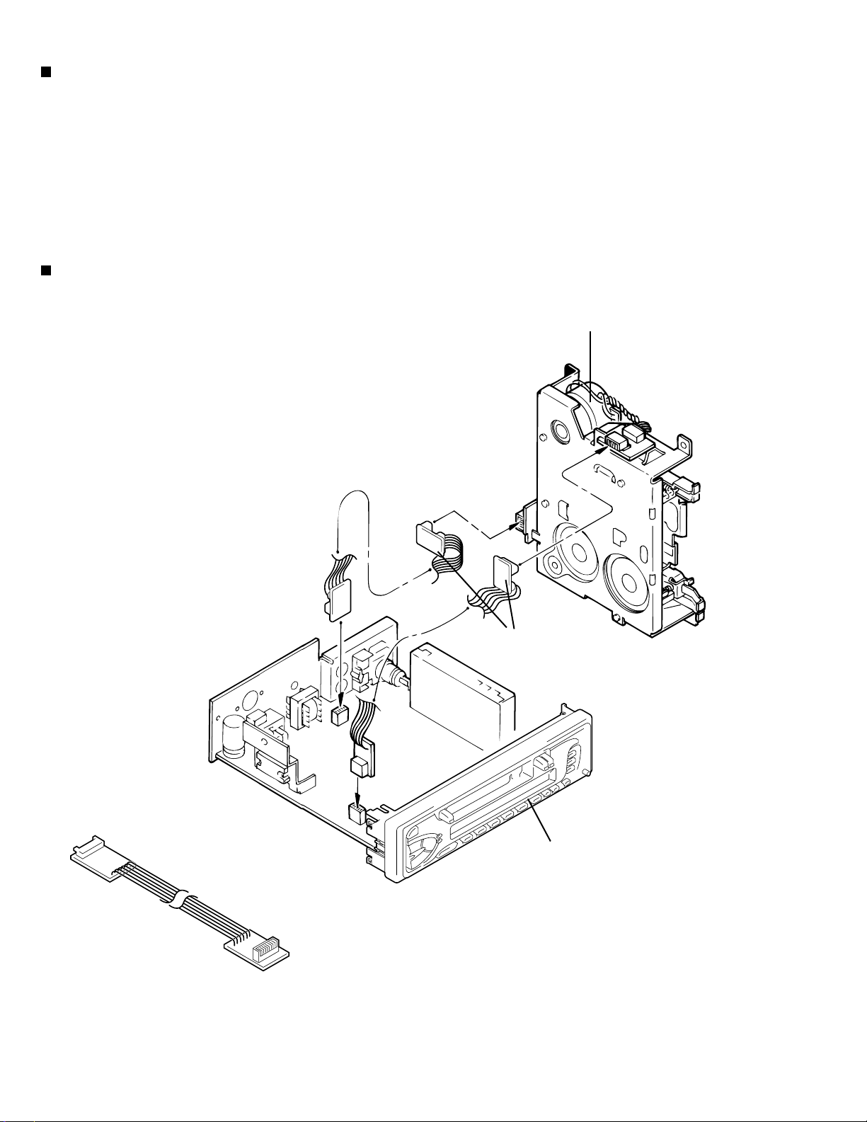
Information for using a Car Audio Service Jig
1. For 1995 and 1996 , we're advancing efforts to make our extension cords common for all car audio products.
Please use this type of extension cord as follows.
2. As a U-shape type top cover is employed, this type of extension cord is needed to check operation of the
mechanism assembly after disassembly.
3. Extension cord : EXTKSRT002-6P ( 6 pin extension cord ) For connection between mechanism assembly
and main board assembly .
Check for mechanism driving section such as motor ,etc..
Disassembly Method
1. Remove the bottom cover.
2. Remove the front panel assembly.
3. Remove the top cover .
4. Install the front panel.
5. Confirm that current is being carried by connecting
an extension cord jig.
Note
Available to connect to the CN701 connector when installing the front panel.
Cassette mechanism
EXTKSRT002-6P
Extension cord
: EXTKSRT002-6P
Main board
Front panel assembly
1-14
Page 15

Mechanism Adjustment Section
Item Adjusting & Confirmation Methods Adjust Std. Value
1.Head azimuth
"Head Height Adjustment"
Note
Adjust the azimuth directly . When you adjust the height using a mirror tape, remove the cassette housing from the
mechanism chassis.
After installing the cassette housing, perform the azimuth
adjustment.
1.load the mirror tape ( SCC-1659 ). Adjust with height
adjustmentscrew (a) and azimuth adjustment screw (b) so
that line "A" of the mirror tape runs in the center between
Lch and Rch in the reverse play mode.
2.After switching from REV to FWD then to REV, check that
the head position set in procedure "1" is not changed.
*If the position has shifted, adjust again and check.
3.Adjust the azimuth screw (b) so that line "B" of the mirror
tape runs in the center between Lch and Rch in the forward
play mode.
"Head Azimuth Adjustment"
1.Load the test tape ( VT724: 1kHz ) and play it back in the
reverse play mode. set the Rch output level to maximum.
2.Load the test tape ( VT703: 10kHz ) and play it back in the
forward play mode. Adjust the Rch and Lch output levels
tomaximum, with azimuth adjustment screw (b).
In this case, the phase difference should be within 45 .
3.Engage the reverse mode and adjust the output level to
maximum, with azimuth adjustment screw (c).
*The phase difference should be 45_Kor more.
4.When switching between forward and reverse modes, the
difference between channels should be within 3dB.
*Between FWD Lch and Rch, REV Lch and Rch.
5.When the test tape ( VT721 : 315Hz ) is played back, the
level difference between channels should be within 1.5dB.
Head shield
The head is at low position
during FWD.
Head shield
The head is at height position
during REV.
Head azimuth
screw
screw (c)
screw (b)
0
Phase
KS-FX201
A Line
B Line
Fixed screw
screw (a)
45
2.T ape Speed and
Wow & Flutter
3.Playback
Frequency
response
1.Check to see if the reading of the frequency counter & Wow
flutter meter is within 2940-3090 Hz( FWD/REV ), and less
than 0.35% ( JIS RMS ).
2.In case of out of specification, adjust the motor with a builtin volume resistor .
1.Play the test tape ( VT724 : 1kHz ) back and set the volume
position at 2V.
2.Play the test tape ( VT739 )back and confirm 0 + 3dB at1kHz/
-
8kHz and -4+2dB at 1kHz/125Hz.
3.When 8kHz is out of specification, it will be necessary to
read adjust the azimuth.
Built-in
volume resistor
T ape Speed
2940-3090Hz
Wow&Flutter
Less than
0.35%
(JIS RMS)
Speaker out
1kHz/8kHz
: 0dB_}3dB,
125Hz/1kHz
: -4dB+2dB,
1-15
Page 16

KS-FX201
Descrption of major ICs
TEA6320T-X (IC931) : E.volume
1.Pin layout
2.Block diagram
10 8 9 7 6
5
12
SDA
1
GND
2
OUTLR
OUTLF
MUTE
TL
B2L
B1L
IVL
ILL
QSL
IDL
ICL
IMD
IBL
IAL
3
4
5
6
7
8
9
10
11
12
13
14
15
16
3.Pin functions
Pin
Symbol
No.
SDA
1
SCL
32
VCC
31
OUTRR
30
OUTRF
29
TR
28
B2R
27
B1R
26
IVR
25
ILR
24
QSR
23
IDR
22
Vref
21
ICR
CD-CH
TAPE
TUNER
20
19
18
17
CAP
IBR
IAR
I/O
Serial data input/output.
I/O
MUTE
21
31
2
19
16
15
13
11
14
22
20
18
17
Functions Functions
POWER
SUPPLY
SOURCE
SELECTOR
23 25 24 26 27 28
VOLUME 1
+20 to -31 dB
LOUDNESS
LEFT
VOLUME 1
+20 to -31 dB
LOUDNESS
RIGHT
Pin
No.
17
Symbol
IAR
BASS
LEFT
+15 dB
LOGIC
BASS
RIGHT
+15 dB
I/O
I
Input A right source.
TREBLE
LEFT
+12 dB
TREBLE
RIGHT
+12 dB
FUNCTION
ZERO CROSS
DETECTOR
VOLUME 2
0 to 55 dB
BALANCE
FENDER REAR
VOLUME 2
0 to 55 dB
BALANCE
FENDER FRONT
HC BUS
REC
VOLUME 2
0 to -55dB
BALANCE
FENDER FRONT
VOLUME 2
0 to -55dB
BALANCE
FENDER REAR
3
4
32
1
29
30
2
3
4
5
6
7
8
9
10
11
12
13
14
15
16
GND
OUTLR
OUTLF
TL
B2L
B1L
IVL
ILL
QSL
IDL
MUTE
ICL
IMO
IBL
IAL
Ground.
output left rear.
O
output left front.
O
Treble control capacitor left channel or
I
input from an external equalizer.
Bass control capacitor left channel or
-
output to an external equalizer.
Bass control capacitor left channel.
Input volume 1. left control part.
I
Input loudness. left control part.
I
Output source selector. left channel.
O
Not used
Not used
Input C left source.
I
Not used
Input B left source.
I
Input A left source.
I
18
19
20
21
22
23
24
25
26
27
28
29
30
31
32
IBR
CAP
ICR
Vref
IDR
QSR
ILR
IVR
B1R
B2R
TR
OUTRF
OUTRR
Vcc
SCL
I
Input B right source.
-
Electronic filtering for supply.
I
Input C right source.
-
Reference voltage (0.5Vcc)
-
Not used
O
Output source selector right channel.
I
Input loudness right channel.
I
Input volume 1. right control part.
-
Bass control capacitor right channel
Bass control capacitor right channel or
O
output to an external equalizer.
Treble control capacitor right channel or
I
input from an external equalizer.
O
Output right front.
O
Output right rear.
-
Supply voltage.
I
Serial clock input.
1-16
Page 17

AN80T05LF (IC781) : Regulator
1.Terminal layout & Block diagram
Reference V oltage
ASO & Peak
Thermal
Protection
Current Protection
KS-FX201
Pre
Drive
1 2 3 4 5 6 7 8 9 10 11 12
ILL
10V
2.Pin function
Pin
No.
1
2
3
4
5
6
7
8
9
10
11
12
Pre
Drive
MODE2 MODE1 STB VDD
5.6V
AMP
Out
AMP VCC ANT COM
Symbol Function
ILL
MODE2
MODE1
STB
VDD
AMP
VCC
ANT
COM
AM
FM
GND
10V power supply for illumination.
When 5V is input,becomes AM. and the antenna output is turned on.
When 5V is input,becomes AM. and the output of FM is switched.
When 5V is input, outputs to ILL,COM,and AMP. It is 0V usually.
5.6V power supply.
Power supply supply to remote amplifier
Back up. connects with ACC with it.
Power supply supply to auto antenna.
8.7V power supply.
The power supply of 8.7V to AM.
The power supply of 8.7V to FM.
Ground
AMP
Out
Pre
Drive
Pre
Drive
8.7VAM8.7VFM8.7V
Pre
Drive
GND
1-17
Page 18

KS-FX201
LC72362N-9920 (IC701) : System control
1. Pin layout
80 to 65
1
64
to to
24
41
25 to 40
2. Pin function
Pin No. Symbol I/O
1
2
3
4
5
6
7
8
9
10
11
12
13
14
15~18
19~22
23~26
27~30
31
32
33~36
37~40
41~43
44
45~48
49~52
53,54
55,56
57~60
61,62
63~66
67
68
69
70
71
72
73
74
75
76
77,78
79
80
PK1/INT1, PK0/INT0
PJ3/DAC3~PJ0/DAC0
PI1/ADI5, PI0/ADI4
PH3/ADI3~PH0/ADI0
XIN
TEST2
PG3/SI0
PG2/SO0
PG1/SCK0
PG0
PF3/SI1
PF2/SO1
PF1/SCK1
PF0
PE3/SI2
PE2/SO2
PE1/SCK2
PE0
PD3~PD0
PC3~PC0
PB3~PB0
PA3~PA0
V DD
PQ0
PP3~PP0
PO3~PO0
PN3~PN1
PN0/BEEP
PM3~PM0
PL3~PL0
PK3, PK2
HOLD
SNS
LCTR
HCTR
EO3
SUBPD
V DD
AMIN
FMIN
V SS
EO2,EO1
TEST1
XOUT
Function
I
4.5MHz crystal oscillator connections
LSI test pin.
I/O
General-purpose input/output and serial input/output shared ports.
Output only port.
O
Key source signal output only ports.
O
Key return signal input only port, of which threshold voltage is designed to be
I
low.
Power supply connections.
O
General-purpose input/output port.
O
O
Output only port.
General-purpose output port/BEEP tone shared output pins.
O
I/O
General-purpose input/output ports.
General-purpose input-output/external interrupt shared port.
I/O
O
General-purpose output port/DAC shared output pins.
I
General-purpose output port/ADC shared input pins.
I
PLL control, CLOCK STOP mode control pin.
I
Voltage sense/general-purpose input pin shared port.
Universal counter (frequency, cycle measurement)/general-purpose input
I
shared input port.
Universal counter/general-purpose input shared input port.
I
O
2nd PLL charge pump output pin.
Sub-charge pump output pin.
O
Power supply connections.
O
AM VCO (local oscillator) input pin.
I
FM VCO (local oscillator) input pin.
I
O
Power supply connections.
Main charge pump output pins.
O
LSI test pin.
4.5MHz crystal oscillator connections
O
1-18
Page 19

KS-FX201
3.Block diagram
XIN
XOUT
FMIN
AMIN
SNS
VDD
VSS
HCTR
LCTR
HOLD
TEST1
TEST2
PA0
PA1
PA2
PA3
PB0
PB1
PB2
BP3
PC0
PC1
PC2
PC3
PD0
PD1
PD2
PD3
PE0
SCK2/PE1
PO2/PE2
SI2/PE3
PF0
SCK1/PF1
SO1/PF2
SI1/PF3
V-DET
DIVIDER REFERENCE DIVIDER SELECTOR
1/16, 1/17
SNSFF
1/2
BUS
DRIV.
LATCH
BUS
DRIV.
LATCH
BUS
DRIV.
LATCH
BUS
DRIV.
LATCH
BUS
DRIV.
LATCH
BUS
DRIV.
PROGRAMMABLE DIVIDER
1/114, 1/124
LATCH
UNIVERSAL
COUNTER
(20bits)
RAM
512 4bits
ROM
12K 16bits
ADDRESS DECODER
PROGRAM COUNTER
STACK
ALU
ADDRESS
DECODER
BUS
DRIVER
INSTRUCTION
DECODER
JUDGE
PHASE
DETECTOR
UNLOCK
F/F
PHASE
DETECTOR
LATCH
LATCH
BUS
DRIV.
LATCH
BUS
DRIV.
LATCH
BUS
DRIV.
BEEP
LATCH
BUS
DRIV.
LATCH
BUS
DRIV.
LATCH
BUS
DRIV.
LATCH
BUS
DRIV.
BUS
DRIV.
SUB
C.P.
MPX
INTERRUPT
LC72362N-9920
E01
E02
SUBPD
EO3
PQ0
PP3
PP2
PP1
PP0
PO3
PO2
PO1
PO0
PN3
PN2
PN1
PN0/BEEP
PM3
PM2
PM1
PM0
PL3
PL2
PL1
PL0
PK3
PK2
PK1/INT1
PK0/INT0
PJ3
PJ2
PJ1
PJ0
PI1/ADI5
PI0/ADI4
PF0
SCK1/PF1
SO1/PF2
SI1/PF3
SIO
LATCH
BUS
DRIV.
ADC
MPX
BUS
DRIV.
PH3/ADI3
PH2/ADI2
PH1/ADI1
PH0/ADI0
1-19
Page 20

KS-FX201
HA13158A (IC981) : Power amp
1. Pin layout
1 ~ 23
2. Block diagram
INVCC
IN1
2
STBY
1
14 18 6
PVCC1PVCC2
INPUTBUFFER1
AMP1
+
3
4
-
5
IN2
IN3
IN4
11
13
23
10
MUTE
INPUTBUFFER2
INPUTBUFFER3
INPUTBUFFER4
PROTECTOR (ASO
SURGE, TSD)
12 22
AMP2
AMP3
AMP4
TAB
7
+
8
-
9
15
+
16
-
17
19
+
20
-
21
1-20
Page 21

HD74HC126P(IC751) :CD CHANGER
KS-FX201
1.Terminal layout
1
1C
2
1A
3
1Y
4
2C
5
2A
6
2Y
7
GND
14
13
12
11
10
2.Pin function
Vcc
4C
4A
4Y
3C
3A
9
3Y
8
Input Output
C
L
H
H
A
X
L
H
Note)
H
:
High level
L
:
Low level
X
:
"H" or "L"
Z
:
Off state of three state output(High impedance)
Y
Z
L
H
UPC1228HA(IC901):Head amp
1
IN1
ANP1
2
NFB1
3
OUT1
VCC
4
GND
5
OUT2
6
7
NFB2
IN2
ANP2
8
UPC1228HA
1-21
Page 22

KS-FX201
VICTOR COMPANY OF JAPAN, LIMITED
MOBILE ELECTRONICS DIVISION
PERSONAL & MOBILE NETWORK BUSINESS UNIT. 10-1,1Chome,Ohwatari-machi,Maebashi-city,Japan
(No.49589)
Printed in Japan
200101(V)
Page 23

1
2
3
4
5
AB C
ANT
J1
AM
1
AM/FM TUNER PA CK
Tuner.Power AMP.Changer/System Controller
DIRECTION BOARD
TO CD CHANGER
SI/SO
SCK
IC751
CD CHANGER
HD74HC126P
BUS SI
BUS SO
BUS SCK
BUS I/O
FM
2
16
TU1
QAU0120-002
MAIN
MOTOR
TAPE /RADIO SW
MUTE SWITCH
CN721CP751
CD Lch
TAPE IN
PROG
SEEK/STOP,
MONO.SD/ST,
S METER,
FM OSC, EO, BAND
CP722
RELAY
BOARD
CP721
TO SPEAKER
CONNECTOR
TO LINE REAR OUT
CP981
Lch Rear
Lch Front
37
IC981
POWER AMP.
HA13158A
1
OUT L Front
4
13
IC931
E.VOLUME
TEA6320T
16
TUNER L
3
15
SDA
SCL
IC701
SYSTEM CONTROL MICON
LC72362N-9595
Lch Rear OUT
TAPE L
CJ921
F/R
KEY 0 - 2
CN901
CJ701
CP901
CP701
LCDDA
LCDCK
LCDCE
HEAD
PROG-SW
CJ901
LCH
F/R
1
IC901
HEAD AMPLIFIER
UPC1228HA
3
LCH
HEAD AMPLIFIER CIRCUIT
LCD1
QLD0335-001
S8 - S52
COM1 - COM3
IC651
LCD DRIVER
LC75823W
KEY
S601 - S620
LCD DRIVER/KEY SWITCH CIRCUT
Block Diagram
KS-FX201
2-1
Page 24

KS-FX201
< MEMO >
2-2
Page 25

Standard schematic diagrams
Receiver & System control circuit section
5
QNZ0009-001
ANT
R774
4
KTC3199/GL/-T
CJ701
VMC0334-001
3
CN721
QGB1214J1-06S
R719
R718
R720
R717
R716
R715
3.3K
3.3K
3.3K
100
100
100
2
CN901
QGB1214J1-06S
1
C772
2.2/50
Q772
KTC3199/GL/-T
D705
D704
D711
MTZJ5.6B-T2
MTZJ5.6B-T2
MTZJ5.6B-T2
10K
R704
47K
R705
C773
0.001
D786
DSK10C-T1
D708
D706
D707
MTZJ5.6B-T2
MTZJ5.6B-T2
MTZJ5.6B-T2
D718
1SS119-041
Q701
KTC3199/GL/-T
1.5K
R773
1K
Q771
LCD.SCK
D709
MTZJ5.6B-T2
TAPE.14V
R772
5V
LCD.SO
LCD.CE
KEY2
KEY1
KEY0
DETACH
PROG
TAPEIN
9V
F/R
TAPE.L
TAPE.R
10K
C771
220/10
R5V
R771
D771
Q3
4.7K
D792
MTZJ9.1C-T2
1SS119-041
KS-FX201
*TU1
KRA102M-T
Q989
ACC.MUTE
D990
1K
R762
1K
R751
R5V
5V
TU-9V
R786
1K
KRC102M-T
MTZ11B-T2
C972
100
*R759
R753
47K
TAPE.L
TAPE.R
9V
C705
10/16
Q784
Q972
KRA102M-T
2.2/10
*R756
HD74HC126P
100
*R755
R754
330K
C132
1/50
C232
1/50
14V
R785
47K
47uH
47K
L782
100
14V
TU.RCH
C13
47K
R757
R758
C988
CD.RCH
100p
TU.LCH
*R63
20K
47/16
CD.LCH
RB72/Q-T2
R792
6.8
*R53
20K
47/16
C934
7.5K
*R54
1/50
*C233
7.5K
*R64
KRA102M-T
R789
R790
1SS119-041
1SS119-041
SI/SO
*C133
IC931
1/50
C933
100/10
L781
47uH
Q789
100K470K
MUTE
SCK
R795
R796
LRO
RRO
R131
22K
C134
TEA6320T
C234
R231
22K
1SS119-041
18K
47K
CD.RCH
0.0082
C236
0.0082
Q782
D781
C783
R163
820
R165
2.2K
2SD2144S/VW/-T
R265
2.2K
R263
820
QNZ0095-001
*CP751
14V
R132
0.15
C135
C136
0.22
0.22
0.15
C235
2.2k 2.2k
R232
2SA1706/ST/-T
1K
R784
Q781
KRC102M-T
KRA102M-T
2200/6.3
10K
R990
SCK
C137
0.033
0.033
C237
47K
R783
Q987
1SS119-041
Q988
KRC102M-T
CJ921
Q161
Q261
SI/SO
C784
10K
D782
2SD2144S/VW/-T
CD.LCH
C150
C138
C250
0.0056 0.0056
1/50
C238
R931
220/10
10/16
10/16
C987
C781
R164
100
R264
100
FM Radio signal
AM Radio signal
CD signal
Tape PB/Main signal
IC981
RRO-
LRO+5VLFO-
RFO+
RFO-
KRC102M-T
LFO+
R971
HA13158A
R951
R972
D974
1SS119-041
4.7K
47K
Q971
CP981
R722
3.3K
3.3K
C932
0.01
LRO
C707
0.01
SCL
D785
RRO
L981
QQR0704-001
DSK10C-T1
R251
27K
470P
C162
R161
27K
R261
27K
470P
C152
R151
27K
C981
2200/16
D981
1N5401TM
R797
12K
R788
R252
82K
C252
470P
R162
82K
R262
82K
C262
470P
R152
82K
R787
100
C984
10/16
ACC.MUTE
C986
C983
C971
C982
C951
10/16
4.7/25
4.7/25
RRO+
0.01
0.01
LRO-
RFO+
RRO+
LRO+
LFO+
RFORROLROLFO-
SDA
C160
1/50
1/50
R721
C931
C260
100/10
1/50
10
C785
1/50
IC781
AN80T05
DSK10C-T1
D784
C985
1SS119-041
L1
4.7uH
R1
10
R2
1K
R3
1K
10/16
R725
R708
R702
R703
R707
0.022
C2
C10
8.2p
FM.OSC
0.1/50
10K
C6
C7
C5
C4
22K
R18
B69
47K
47K
47K
47K
47K
0.01
C11
0.1/50
D1
D2
C3
1SS119-041
1SS119-041
Q1
2SA1706/ST/-TKTA1267/YG/-T
R4
R5
Q2
KRC102M-T
IFREQ
MONO
ACC
1K
1SS119-041
1SS119-041
1SS119-041
BAND
*D701
D714
D715
10K
TU-9V
2200/16
EO
RB721Q-T2
14V
C786
D719
R727
47K
10K
R6
D791
1SS119-041
R17
2.2K
R9
R14
R15
IFREQ
1.5M
4.7M
TAPEIN
Q5
KRC102M-T
SD/ST
MONO
SCL
*IC701
LC72362N-XXXX
PROG
F/R
SD/ST
0.1/50
C8
0.01
C15
SDA
4.7K
R724
DETACH
R52
S.METER
LCD.CE
LCD.SCK
1K
R723
BUS.INT
R51
1/50
1/50
C231
C131
TU.RCH
TU.LCH
LCD.SO
BAND
R61
C9
R62
BUS.I/O
MUTE
0.01
IF.C
BUS.SO
BUS.SCK
MEM.DET
BUS.SI
S.METER
KEY2
MUTE
BUS.INT
BUS.SCK
BUS.I/O
BUS.SO
BUS.SI
C706
0.01
R710
R709
R712
*C12
100p
D973
L783
47uH
1K
R761
1K
R763
*R752
10K
10K
*R760
*IC751
0.01
*C751
R764
47K
C702
22P
X701
C701
QAX0406-001Z
27P
EO
FM.OSC
47K
R726
D716
IF.C
1SS119-041
KEY0
KEY1
3.3K
3.3K
C703
100/6.3
R713
R714
4.7K
4.7K
3.3K
C14
100p
C704
0.22
2SA1706/ST/-T
Q783
NOTE:/s/C/jes/3161ma.001
KS-FX200J/KS-F315EE/KS-FX201USERIES
FSDH3161-006AW 1/3
ABCD E F G
2-3
Page 26

KS-FX201KS-FX201
Head amplifier circuit section
5
CJ901
QGA2002C1-05
4
C203
C202
C201
100p
0.47/50
820p
CP722
QGA2002F1-06
3
R204
330k
R203
C204
IC901
UPC1228HA
R201
0.01
C205
100
47/6.3
C901
100/10
100
R901
R101
R104
330k
C105
C104
0.01
R103
47/6.3
C103
100p
100
C102
C101
0.47/50
820p
2
CP721
QGB1214K1-06S
CP901
QGB1214K1-06S
Tape PB/Main signal
1
NOTE:/s/C/jes/3161me.001
KS-FX200J/KS-F315EE/KS-FX201USERIES
FSDH3161-006MW 2/3
2-4
HABC DEFG
Page 27

KS-FX201
LCD driver & Operation switch circuit section
5
MA152WK-X
LCD1
QLD0145-001
S8S9S10
S11
S12
S13
S14
S15
S16
S17
S18
S19
S20
S21
S22
R661
1.5k
C651
150k
D653
MA152WA-X
D652
MA152WA-X
R601
270
S601
R606 R607 R608
270 330 390
S607
R612 R613 R614
270 330 390
S614 S615 S616 S617
0.1
C652
4.7/6.3
R662
47k
C653
680p
R602
330
S603
S608 S609 S610
S602
S49
S50
S51
S52
COM1
COM2
COM3
COM2
COM3
S52
S23
S24
S25
S26
S27
S28
S29
S30
S31
S32
S33
S34
S35
S36
S37
S38
S39
S40
S41
S42
S43
S44
S45
S46
S47
S48
S48
S47
S46
S45
S44
S43
S42
S41
S40
S39
S38
S37
S33
S34
S35
S36
S32
S31
S30
S29
S28
S27
IC651
LC75823W
S9
S8
S10
S11
S604 S605
R609
470
R615 R616
470 560
S26
S25
S24
S23
S22
S21
S20
S19
S18
S17
S12
S13
S14
S15
S16
R605R603 R604
560390 470
R610 R611
560 820
S611
S618
S606
S612
S619
COM1
S51
S49
S50
S613
R617
820
S620
CP701
VMC0335-001
4
R633
820
D623
R631
820
R634
820
D603
D602
R632
R640 R641
820
820
820
R643
D618
D619
D620
R644
R645
820
R642
330 330
D621
D622
3
2
D601
820
820
820
820
820
D614
D615
D616
R646
R647
D612 D611D613
R648
R649
D609
D610
D624
R650
R651
10K
10K
10K
R622
R621
R623
510
510
PL603
PL601
D605 D604
MA152WK-X
1
NOTE:/S/C/jes/3211sw.001
KS-FX200J/201U SERIES KS-F315EE
FSDH3161-006 3/3
ABCD E F G
2-5
Page 28

Printed circuit boards
Main boards
KS-FX201KS-FX201
5
4
3
2
FSMW1067C
CP722
T03
AMANT
FMANT
AMDX/LO
FMDX/LO
GND
FMVT
GND
GND
AMVCC
GND
FM/AMOSC
FMVCC
FM/AMVCC
AMVT
GND
L-CH
R-CH
GND
NC
SEEK/STOP
S.METER
SD/ST
SNC
COMP.OUT
FM/AMVCC
MUTEDRIVE
C105
CP721
31
7
8
CJ921
D771
J1
C10
C771
R771
D719
TU1
R773
R772
C773
R3
R2
5
L1
C3
D704
R715
C5
10
15
C4
C6
20
C7
R14
C15
25
Q5
B
D705
R716
R717
C786
D706
D2
D1
R18
C772
E
B
R774
R7
B
E
Q771
Q772
C2
E
D792
C11
E
R712
D711
1
214
E
C1
Q1
B
R1
R6
R4
B
Q3
R5
B
Q2
R17
D791
R9
R15
R713
R714
R708
E
C8
R724
C706
R725
L782
R720
CJ701
C9
D707
4
6
6
R51
R52
R63
C14
R709
C12
R718
D708
15
R719
D709
D981
CP751
C132
C934
C233
C236
C131
R132
R131
C136
16
17
C235
R61
C933
R710
64
65
C704
C703
C133
1
IC931
C232
R54
R53
C231
R62
R64
R707
R702
C13
R703
D716
R726
R723
R792
C705
D786
FSMW1067B
C203
R204
R201
C707
C135
C134
1
32
C237
C234
C238
R265
EB
Q261
D261
R761
41
1
80
C701
R763
C702
X701
1
R101
R104
C103
IC901
8
C205
1
R
S.GND
L981
C137
C150
C138
R721
C260
C250
R232
R231
R263
Q161
Q971
BE
BE
R972
D974
R165
R727
D713
D701
25
24
1
14
C751
R752
R757
R759
R760
R722
R756
L
C160
E
R931
R103
D714
R203
GND
R789
D161
R785
R762
R163
Q784
C971
D715
C104
C901
R901
6
9V
F/R
R164
C101
1
C102
CJ901
5
C204
C201
C202
CP901
CP981
D718
6
R951
C981
12
8
C982
C986
23
22
IC981
2
1
C988
Q787
D784
C983
R797
E
Q783
B
C985
E
B
Q781
C987
C783
C781
C984
D785
CN721
1
B
9
1
R787
C931
C932
C262
C252
R251
R262
R261
R162
R264
R161
R152
R151
C951
EB
R790
Q972
E
B
R795
Q789
R796
B
D781
D782
R990
L781
Q987
EB
BE
Q988
R788
R755
R751
R754
7
IC751
8
R753
R758
R252
C162
C152
C972
R971
R786
EB
Q989
D973
R783
B
L783
E
Q782
R764
C784
C785
R784
D990
R704
B
E
Q701
D705
12
IC781
1
1
NOTE:KS-FX200J,KS-FX201 FSMW1067-0203
/d2/c/jes/1067ma/1067mo
2-6
HABC DEFG
Page 29

LCD Driver & Operation switch board
KS-FX201
5
4
3
(Solder side) (Parts side)
R640
S601
D623
R601
S03
S603
FSMW1077A
S606
S608
S609
S610
S611
S612
R608
R607
R609
R611
D603
D602
R610
LCD1
D614
D604
D601
D605
R605
D620
R604
S602
R602
D618
S607
R642
R641
R606
D619
R603
D622
S605
PL601
R643
S604
D621
R631
R633
FSMW1077A
R651
R650
R662
C653
PL601
17
33
R634
R632
1
49
2
1
Note:KS-FX200,KS-FX201
/d2/c/jes/1077sw/1077mo
D615
S613
D616
S614
R612
D611
S615
R613
D613
PL603
D612
S616
R615
D624
S618
R647
S619
R646
S617
D610
R617
R616
R645
R644
R649
R648
D655
S620
D609
D653
R661
C652
C651
D652
D654
T03
PL603
R663
CP701
R623
R622
R621
R614
ABC
2-7
Page 30

PARTS LIST
[ KS-FX201 ]
* All printed circuit boards and its assemblies are not available as service parts.
Areas suffix
U --------------------- Other Areas
KS-FX201
- Contents -
Exploded view of general assembly and parts list
Cassette mechanism assembly and parts list
Electrical parts list
Packing materials and accessories parts list
3- 2
3- 5
3-10
3-14
3-1
Page 31

KS-FX201
Exploded view of general assembly and parts list
Block No.
61
60
M
M
1
M
Main board
52
50
LCD / Switch board
30
1
28
3-2
15
Page 32

KS-FX201
Parts list (General assembly)
Item Parts number Parts name Area
A
1 FSJC1053-006 FRONT PANEL 1
2 ZCKSFX12J-FB FRONT CHASS.ASSY 1
2-1 FSJC1055-001 FRONT CHASSIS 1
2-2 FSJC4003-027 CASSETTE LID 1
2-3 VKW4947-002 DOOR SPRING 1
3 QYSPSPT2625Z MINI SCREW 1
4 FSKM2005-002 MECHA BRACKET 1
5 QYSDST2605Z SCREW 2 PCB+MECHA
6 QYSDSP2604Z SCREW 4 MECHA+M.BRACKET
7 FSJC1029-012 TOP CHASSIS 1
8 FSMH3001-002 SIDE PANEL 1
9 FSKM3011-002 BOTTOM COVER 1
10 FSMA3004-003 INSULATOR 1
11 QYSDST2605Z SCREW 4 CHASSIS+MECHA BKT
12 FSKZ4005-001 SCREW 3
13 QYSDST2604Z SCREW 2 CHASSIS+REAR BKT
14 QYSDST2606Z SCREW 2 CHASSIS+MAIN PWB
15 FSJD3022-00E FINDER ASSY 1
17 FSKS3010-001 LOCK LEVER 1
18 FSKW4005-003 TORSION SPRING 1
19 FSXP3026-002 RLS KNOB 1
20 FSKW3002-004 COMP.SPRING 1
21 --------------- CASSETTE MECHA 1 CDS-363SJ1
22 VKL7821-001 EJECT LEVER 1
24 FSJK3014-001 LIGHT LENS 1
25 FSYH4036-031 SHEET 1 PRESET BTN
26 FSXP2035-108 PRESET BUTTON 1
27 FSXP4005-026 BBE BUTTON 1
28 FSXP2044-001 COMBO BUTTON 1
29 FSXP3053-002 POWER BUTTON 1
30 FSXP2034-037 D.FUNC BUTTON 1 FM/AM/CD-CH
31 FSXP3068-001 PUSH BUTTON 1
33 FSXP3066-001 FF BUTTON 1
34 FSXP3067-001 REW BUTTON 1
35 FSXP3065-001 EJECT BUTTON 1
36 FSKW3002-003 COMP. SPRING 3
37 FSXP3055-001 DETACH BUTTON 1
38 FSKW3002-012 COMP. SPRING 1 FOR DETACH BUTTON
39 FSJC1054-001 REAR COVER 1
40 VKZ4777-001 MINI SCREW 4 F.PANEL+REAR COVER
41 GE30126-002B NAME PLATE 1
42 VMA4652-001SS EARTH PLATE 1
43 FSKL4018-00B IC BRACKET 1
44 QMFZ047-100-T FUSE
A
45 FSKM3010-011 REAR BRACKET 1
46 QYSDST2606Z SCREW 1 REAR BKT+ANT JACK
50 FSYH4076-001 LIGHTING SHEET 1
51 QNZ0439-001 RUBBER CONNE 1
Q'ty Description
1-6,DISP,RPT/SCAN
LOUD,MD/RND
1
Block No. M1MM
3-3
Page 33

KS-FX201
Parts list (General assembly)
Item Parts number Parts name Area
A
52 FSJK3034-001 LCD LENS 1
54 FSYH3022-001 LCD CASE 1
55 FSKS3021-001 LENS CASE 1
56 QYSDST2606Z SCREW 2 REAR BKT+CONNECTOR
60 QYSDST2606Z SCREW 1 REAR BKT+CD IN JACK
61 QYSDSF3006Z SCREW 1 REAR BKT+PIN JACK
LCD 1 QLD0145-001 LCD MODULE 1
Q'ty Description
Block No. M1MM
3-4
Page 34

Cassette mechanism assembly and parts list
CDS-363SJ1
Block No.
M
2
M
KS-FX201
M
30
12
66
81
109
78
49
72
24
21
32
100
89
120
116
97
57
106
2
105
109
123
119
45
46
107
23
96
53
31
93
114
121
19
65
71
67
61
61
107
110
25
58
118
83
8
76
68
69
47
109
3
115
109
20
22
62
5
6
73
109
54
42
70
40
107
43
44
63
79
35
117
38
4
117
39
106
37
41
7
77
107
10
1
50
82
48
26
9
74
87
106
86
122
94
95
101
117
85
15
16
80
3-5
Page 35

KS-FX201
)
)
)
)
)
)
)
)
)
)
)
)
)
)
)
Parts list (Cassette mechanism)
Item Parts number Parts name Area
A
1 X-0363-1001S MAIN CHASSIS AS 1
2 X-0363-1002S HEAD PLATE ASSY 1
3 X-0363-1004S FR CONVERT ARM 1(A
4 X-0363-6001S REEL BASE ASSY 1
5 X-0363-6007S LEVER BRACKET 1(HD
6 X-0363-6003S TU GEAR ARM ASS 1
7 X-0363-6004S PINCH ARM(R) AS 1
8 X-0363-6005S PINCH ARM(F) AS 1
9 X-0363-6006S DETECTOR CAM AS 2(V
10 X-0363-2005S REEL SPINDLE AS 2
12 X-0363-1019S EJ.CAM LOCK ASS 1
15 1-0363-6010S FLYWHEEL ASSY(F 1 CPL
16 1-0363-6011S FLYWHEEL ASSY(R 1 CPL
19 1-0036-1065S FF LEVER(JVC
20 1-0036-1066S REW LEVER(JVC
21 1-0036-1007S EJECT LEVER 1
22 1-0036-1013S LOCK ARM 1
23 1-0036-1015S SPG SUPPORT PLT 1
24 1-0036-1018S CENTER PLATE 1
25 1-0036-1023S CHANGE LEVER(B
26 1-0036-1026S FR ARM(B
30 1-0138-1002S CASSETTE HANGER 1(X
31 1-0138-1006S ADJUSTER SHIM 1(X
32 1-0138-1010S CASSETTE HOLDER 1(X
35 1-0363-1003S EJECT CAM 1
37 1-0036-2001S IDLE GEAR 1
38 1-0036-2003S REDUCTION GEAR 1(B
39 1-0036-2004S REDUCTION GEAR 1(A
40 1-0036-2007-5S RATCHET 1
41 1-0036-2009S SENSOR ARM 1
42 1-0036-2010S SELECTOR GEAR 1
43 1-0036-2014S DETECTOR GEAR 1
44 1-0038-2014S GEAR LOCK ARM 1
45 1-0038-2018S TAPE GUIDE 1
46 1-0363-2006S ADJUSTER LINK(B 1
47 1-0138-2005-3S ADJUSTER ARM 1 BLUE
48 1-0036-2005S PULLEY GEAR 1
49 1-0032-2007S TAPE HOOKER 1
50 1-0058-2021-5S IDLE PULLEY(A
53 1-0363-3018S FF ROLLER 1
54 1-0036-3018S COLLAR 1(SELECTOR GEAR
57 1-0363-3007S HP ROLLER(A
58 1-0363-3011S PROGRAM ROLLER 1
61 1-0036-4001S FF/REW LEVER SP 2
62 1-0036-4002S LOCK LEVER SPG 1
63 1-0036-4003S G.LOCK ARM SPG 1
65 1-0036-4006S HEAD PLATE SPG 1
66 1-0036-4007S EJ.CAM LOCK SPG 1
Q'ty Description
1
1
1
1
1
1
Block No. M2MM
3-6
Page 36

KS-FX201
)
)
)
)
)
)
Parts list (Cassette mechanism)
Item Parts number Parts name Area
A
67 1-0036-4008S PROGRAM ARM SPG 1
68 1-0036-4010S ADJUSTER ARM SP 1(A
69 1-0036-4011S ADJUSTER ARM SP 1(B
70 1-0036-4015S DASH SPG 1
71 1-0036-4017S S.SELECT ARM SP 1
72 1-0036-4023S CENTER PLT SP(B 1
73 1-0038-4014S RATCHET SPG 1
74 1-0138-4001S BACK TENSION SP 2
76 1-0363-4003S PINCH ARM SPG F 1
77 1-0363-4004S PINCH ARM SPG R 1
78 1-0363-4005S EJECT LEVER SPG 1
79 1-0036-4005S EJECT CAM SPG 1
80 1-0036-5020S MAIN BELT(AL
81 1-0363-5007S RETURN LINK 1
82 1-0036-5001S SUB BELT 1
83 1-0363-5003S SELECTOR LINK(B 1
85 1-0036-7002S WIRE(A
86 1-0036-7003S WIRE(B
87 1-0036-7073S WIRE(AL
89 X-0363-7006S MOTOR ASSY 1
93 1-0363-7001S MUTE SWITCH 1
94 1-0363-7002S SLIDE SWITCH 1
95 1-0363-7008S SLIDE SW PWB 1
96 1-0036-7016S HEAD 1
97 1-0363-7005S POWER SWITCH 1
100 1-0036-7089S 6P WIRE ASY(JVC 1
101 1-0036-7088S 5P WIRE ASY(JVC 1
105 2-1816-0032-E8S LMW-S 2
106 2-1812-0030-D2S PSW-S 3
107 1-0036-5024S PSW(REEL)B 5
109 2-1712-0050-16S E RING 5
110 2-1712-5060-16S E RING 1
114 1-0363-7015S MUTE SW PWB 1
115 2-1331-7040-C2S SCREW S 1
116 2-1331-7060-C2S SCREW S 1
117 2-1382-0030-C2S SCREW B 5
118 2-1332-0040-C1S SCREW S 1
119 2-1032-0070-C2S SCREW 2
120 2-1032-0025-C2S SCREW 2
121 2-1012-0040-C2S SCREW 1
122 2-1012-0030-F2S SCREW 1
123 1-0138-5002S AZIMUTH SCREW 3
Q'ty Description
1
1 BLACK 60MM
1 RED 60MM
1 YELLOW 55MM
Block No. M2MM
3-7
Page 37

KS-FX201
Grease point 1/2
Grease
FL-942
SW-902
SW522B
FG-84M
C68
1
Reverse side
A
24
3-8
2
72
Page 38

Grease point 2/2
KS-FX201
19
20
5
35
30
12
3
38
16
39
42
37
43
4
15
3-9
Page 39

KS-FX201
Electrical parts list (Main board)
Item
A
C 2 QDX11EK-223Z C CAPACITOR
C 3 QEKJ1HM-104Z E CAPACITOR 0.1MF 20% 50V
C 4 QEKJ1HM-104Z E CAPACITOR 0.1MF 20% 50V
C 5 QEKJ1CM-106Z E CAPACITOR 10MF 20% 16V
C 6 QDX11EK-223Z C CAPACITOR
C 7 QDX11EK-223Z C CAPACITOR
C 8 QERF1HM-104Z E CAPACITOR 0.1MF 20% 50V
C 9 QDYB1CM-103Y C CAPACITOR
C 11 QDYB1CM-103Y C CAPACITOR
C 15 QDYB1CM-103Y C CAPACITOR
C 101 QDGB1HK-821Y C CAPACITOR
C 102 QEKJ1HM-474Z E CAPACITOR 0.47MF 20% 50V
C 103 QCBB1HK-101Y C CAPACITOR 100PF 10% 50V
C 104 QEKJ0JM-476Z E CAPACITOR 47MF 20% 6.3V
C 105 QFV61HJ-103Z MF CAPACITOR 0.01MF 5% 50V
C 131 QEKJ1HM-105Z E CAPACITOR 1.0MF 20% 50V
C 132 QEKJ1HM-105Z E CAPACITOR 1.0MF 20% 50V
C 133 QEKJ1HM-105Z E CAPACITOR 1.0MF 20% 50V
C 134 QFLK1HJ-822Z M CAPACITOR 8200PF 5% 50V
C 135 QFV61HJ-154Z MF CAPACITOR 0.15MF 5% 50V
C 136 QFV61HJ-224Z MF CAPACITOR 0.22MF 5% 50V
C 137 QFV61HJ-333Z MF CAPACITOR 0.033MF 5% 50V
C 138 QFLK1HJ-562Z M CAPACITOR 5600PF 5% 50V
C 150 QERF1HM-105Z E CAPACITOR 1.0MF 20% 50V
C 152 QCBB1HK-471Y C CAPACITOR 470PF 10% 50V
C 160 QEKJ1HM-105Z E CAPACITOR 1.0MF 20% 50V
C 162 QCBB1HK-471Y C CAPACITOR 470PF 10% 50V
C 201 QDGB1HK-821Y C CAPACITOR
C 202 QERF1HM-474Z E CAPACITOR 0.47MF 20% 50V
C 203 QCBB1HK-101Y C CAPACITOR 100PF 10% 50V
C 204 QEKJ0JM-476Z E CAPACITOR 47MF 20% 6.3V
C 205 QFV61HJ-103Z MF CAPACITOR 0.01MF 5% 50V
C 231 QERF1HM-105Z E CAPACITOR 1.0MF 20% 50V
C 232 QERF1HM-105Z E CAPACITOR 1.0MF 20% 50V
C 233 QERF1HM-105Z E CAPACITOR 1.0MF 20% 50V
C 234 QFLK1HJ-822Z M CAPACITOR 8200PF 5% 50V
C 235 QFV61HJ-154Z MF CAPACITOR 0.15MF 5% 50V
C 236 QFV61HJ-224Z MF CAPACITOR 0.22MF 5% 50V
C 237 QFV61HJ-333Z MF CAPACITOR 0.033MF 5% 50V
C 238 QFLK1HJ-562Z M CAPACITOR 5600PF 5% 50V
C 250 QERF1HM-105Z E CAPACITOR 1.0MF 20% 50V
C 252 QCBB1HK-471Y C CAPACITOR 470PF 10% 50V
C 260 QERF1HM-105Z E CAPACITOR 1.0MF 20% 50V
C 262 QCBB1HK-471Y C CAPACITOR 470PF 10% 50V
C 701 QDUB1HJ-270Y C CAPACITOR
C 702 QDCB1HJ-220Y C CAPACITOR
C 703 QERF0JM-107Z E CAPACITOR 100MF 20% 6.3V
C 704 QFV61HJ-224Z MF CAPACITOR 0.22MF 5% 50V
C 705 QERF1CM-106Z E CAPACITOR 10MF 20% 16V
C 706 QDYB1CM-103Y C CAPACITOR
C 707 QFV61HJ-103Z MF CAPACITOR 0.01MF 5% 50V
C 751 QDYB1CM-103Y C CAPACITOR
C 771 QERF1AM-227Z E CAPACITOR 220MF 20% 10V
C 772 QERF1HM-225Z E CAPACITOR 2.2MF 20% 50V
C 773 QDGB1HK-102Y C CAPACITOR
C 781 QEKJ1CM-106Z E CAPACITOR 10MF 20% 16V
C 783 QETN0JM-228Z E CAPACITOR 2200MF 20% 6.3V
C 784 QERF1AM-227Z E CAPACITOR 220MF 20% 10V
C 785 QERF1HM-105Z E CAPACITOR 1.0MF 20% 50V
C 786 QETM1AM-228 E CAPACITOR 2200MF 20% 10V
C 901 QEKJ1AM-107Z E CAPACITOR 100MF 20% 10V
C 931 QEKJ1AM-107Z E CAPACITOR 100MF 20% 10V
C 932 QDYB1CM-103Y C CAPACITOR
Parts number Parts name Area
Block No. 01
Remarks
Item
A
C 933 QERF1AM-107Z E CAPACITOR 100MF 20% 10V
C 934 QERF1CM-476Z E CAPACITOR 47MF 20% 16V
C 951 QERF1EM-475Z E CAPACITOR 4.7MF 20% 25V
C 971 QERF1EM-475Z E CAPACITOR 4.7MF 20% 25V
C 972 QERF1AM-227Z E CAPACITOR 220MF 20% 10V
C 981 QEZ0337-228 E CAPACITOR 2200MF
C 982 QDYB1CM-103Y C CAPACITOR
C 983 QDYB1CM-103Y C CAPACITOR
C 984 QERF1CM-106Z E CAPACITOR 10MF 20% 16V
C 985 QRE141J-472Y C RESISTOR 4.7K 5% 1/4W
C 986 QERF1CM-106Z E CAPACITOR 10MF 20% 16V
C 987 QEKJ1CM-106Z E CAPACITOR 10MF 20% 16V
C 988 QERF1CM-476Z E CAPACITOR 47MF 20% 16V
CJ701 VMC0334-001 CONNECTOR TO FRONT PANEL
CJ901 QGA2002C1-05 CONNECTOR
CJ921 QNN0183-001 PIN JACK
CN721 QGB1214J1-06S CONNECTOR TO MECHA
CN901 QGB1214J1-06S CONNECTOR TO MECHA
CP721 QGB1214K1-06S CONNECTOR
CP722 QGA2002F1-06 CONNECTOR
CP751 QNZ0095-001 CONNECTOR CH CONNECTOR
CP901 QGB1214K1-06S CONNECTOR
CP981 QNZ0002-001 16P CONNECTOR
D 1 1SS119-041 SI DIODE
D 2 1SS119-041 SI DIODE
D 161 1SS119-041 SI DIODE
D 261 1SS119-041 SI DIODE
D 701 1SS119-041 SI DIODE
D 704 MTZJ5.6B-T2 ZENER DIODE
D 705 MTZJ5.6B-T2 ZENER DIODE
D 706 MTZJ5.6B-T2 ZENER DIODE
D 707 MTZJ5.6B-T2 ZENER DIODE
D 708 MTZJ5.6B-T2 ZENER DIODE
D 709 MTZJ5.6B-T2 ZENER DIODE
D 711 MTZJ5.6B-T2 ZENER DIODE
D 714 1SS119-041 SI DIODE
D 716 1SS119-041 SI DIODE
D 718 1SS119-041 SI DIODE
D 719 RB721Q-T2 S.B.DIODE
D 771 MTZJ9.1C-T2 ZENER DIODE
D 781 1SS119-041 SI DIODE
D 782 1SS119-041 SI DIODE
D 784 DSK10C-T1 DIODE
D 785 DSK10C-T1 DIODE
D 786 DSK10C-T1 DIODE
D 791 1SS119-041 SI DIODE
D 792 1SS119-041 SI DIODE
D 973 1SS119-041 SI DIODE
D 974 1SS119-041 SI DIODE
D 981 1N5401-TM DIODE
D 990 MTZ11B-T2 SI DIODE
IC701 LC72362N-9920 IC
IC751 HD74HC126P IC
IC781 AN80T05LF IC
IC901 UPC1228HA IC
IC931 TEA6320T-X IC
IC981 HA13158A IC
J 1 QNZ0009-001 CAR ANT JACK
L 1 QQL231K-4R7Y INDUCTOR
L 781 QQL231K-470Y INDUCTOR
L 782 QQL231K-470Y INDUCTOR
L 783 QQL231K-470Y INDUCTOR
L 981 QQR0704-001 CHOKE COIL
Parts number Parts name Area
Remarks
3-10
Page 40

KS-FX201
Q
Q
Q
Q
Q
Q
Q
Q
Q
Q
Q
Q
Q
Q
Q
Q
Q
Q
Q
Electrical parts list (Main board)
Item
A
R 1 QRE141J-100Y C RESISTOR 10 5% 1/4W
R 2 QRE141J-102Y C RESISTOR 1.0K 5% 1/4W
R 3 QRE141J-102Y C RESISTOR 1.0K 5% 1/4W
R 4 QRE141J-103Y C RESISTOR 10K 5% 1/4W
R 5 QRE141J-102Y C RESISTOR 1.0K 5% 1/4W
R 6 QRE141J-103Y C RESISTOR 10K 5% 1/4W
R 9 QRE141J-103Y C RESISTOR 10K 5% 1/4W
R 14 QRE141J-155Y C RESISTOR 1.5M 5% 1/4W
R 15 QRE141J-475Y C RESISTOR 4.7M 5% 1/4W
R 17 QRE141J-222Y C RESISTOR 2.2K 5% 1/4W
R 18 QRE141J-223Y C RESISTOR 22K 5% 1/4W
R 51 QRE141J-122Y C RESISTOR 1.2K 5% 1/4W
R 52 QRE141J-472Y C RESISTOR 4.7K 5% 1/4W
R 53 QRE141J-203Y C RESISTOR 20K 5% 1/4W
R 54 QRE141J-752Y C RESISTOR 7.5K 5% 1/4W
R 61 QRE141J-122Y C RESISTOR 1.2K 5% 1/4W
R 62 QRE141J-472Y C RESISTOR 4.7K 5% 1/4W
R 63 QRE141J-203Y C RESISTOR 20K 5% 1/4W
R 64 QRE141J-752Y C RESISTOR 7.5K 5% 1/4W
R 101 QRE141J-153Y C RESISTOR 15K 5% 1/4W
R 103 QRE141J-101Y C RESISTOR 100 5% 1/4W
R 104 QRE141J-334Y C RESISTOR 330K 5% 1/4W
R 131 QRE141J-223Y C RESISTOR 22K 5% 1/4W
R 132 QRE141J-222Y C RESISTOR 2.2K 5% 1/4W
R 151 QRE141J-273Y C RESISTOR 27K 5% 1/4W
R 152 QRE141J-823Y C RESISTOR 82K 5% 1/4W
R 161 QRE141J-273Y C RESISTOR 27K 5% 1/4W
R 162 QRE141J-823Y C RESISTOR 82K 5% 1/4W
R 163 QRE141J-821Y C RESISTOR 820 5% 1/4W
R 164 QRE141J-101Y C RESISTOR 100 5% 1/4W
R 165 QRE141J-222Y C RESISTOR 2.2K 5% 1/4W
R 201 QRE141J-153Y C RESISTOR 15K 5% 1/4W
R 203 QRE141J-101Y C RESISTOR 100 5% 1/4W
R 204 QRE141J-334Y C RESISTOR 330K 5% 1/4W
R 231 QRE141J-223Y C RESISTOR 22K 5% 1/4W
R 232 QRE141J-222Y C RESISTOR 2.2K 5% 1/4W
R 251 QRE141J-273Y C RESISTOR 27K 5% 1/4W
R 252 QRE141J-823Y C RESISTOR 82K 5% 1/4W
R 261 QRE141J-273Y C RESISTOR 27K 5% 1/4W
R 262 QRE141J-823Y C RESISTOR 82K 5% 1/4W
R 263 QRE141J-821Y C RESISTOR 820 5% 1/4W
R 264 QRE141J-101Y C RESISTOR 100 5% 1/4W
R 265 QRE141J-222Y C RESISTOR 2.2K 5% 1/4W
R 702 QRE141J-473Y C RESISTOR 47K 5% 1/4W
Parts number Parts name Area
1 2SA1706/ST/-T TRANSISTOR
2 KRC102M-T D.TRANSISTOR
3 KTA1267/YG/-T TRANSISTOR
5 KRC102M-T D.TRANSISTOR
161 2SD2144S/VW/-T TRANSISTOR
261 2SD2144S/VW/-T TRANSISTOR
701 KTC3199/GL/-T TRANSISTOR
771 KTC3199/GL/-T TRANSISTOR
772 KTC3199/GL/-T TRANSISTOR
781 KRC102M-T D.TRANSISTOR
782 2SA1706/ST/-T TRANSISTOR
783 KRC102M-T D.TRANSISTOR
784 2SA1706/ST/-T TRANSISTOR
789 KRA102M-T D.TRANSISTOR
971 KRC102M-T D.TRANSISTOR
972 KRA102M-T D.TRANSISTOR
987 KRA102M-T D.TRANSISTOR
988 KRC102M-T D.TRANSISTOR
989 KRA102M-T D.TRANSISTOR
Block No. 01
Remarks
Item
A
R 703 QRE141J-473Y C RESISTOR 47K 5% 1/4W
R 704 QRE141J-103Y C RESISTOR 10K 5% 1/4W
R 705 QRE141J-473Y C RESISTOR 47K 5% 1/4W
R 707 QRE141J-473Y C RESISTOR 47K 5% 1/4W
R 708 QRE141J-473Y C RESISTOR 47K 5% 1/4W
R 709 QRE141J-472Y C RESISTOR 4.7K 5% 1/4W
R 710 QRE141J-472Y C RESISTOR 4.7K 5% 1/4W
R 712 QRE141J-332Y C RESISTOR 3.3K 5% 1/4W
R 713 QRE141J-332Y C RESISTOR 3.3K 5% 1/4W
R 714 QRE141J-332Y C RESISTOR 3.3K 5% 1/4W
R 715 QRE141J-101Y C RESISTOR 100 5% 1/4W
R 716 QRE141J-101Y C RESISTOR 100 5% 1/4W
R 717 QRE141J-101Y C RESISTOR 100 5% 1/4W
R 718 QRE141J-332Y C RESISTOR 3.3K 5% 1/4W
R 719 QRE141J-332Y C RESISTOR 3.3K 5% 1/4W
R 720 QRE141J-332Y C RESISTOR 3.3K 5% 1/4W
R 721 QRE141J-332Y C RESISTOR 3.3K 5% 1/4W
R 722 QRE141J-332Y C RESISTOR 3.3K 5% 1/4W
R 723 QRE141J-102Y C RESISTOR 1.0K 5% 1/4W
R 724 QRE141J-472Y C RESISTOR 4.7K 5% 1/4W
R 725 QRE141J-473Y C RESISTOR 47K 5% 1/4W
R 726 QRE141J-473Y C RESISTOR 47K 5% 1/4W
R 727 QRE141J-473Y C RESISTOR 47K 5% 1/4W
R 751 QRE141J-102Y C RESISTOR 1.0K 5% 1/4W
R 752 QRE141J-103Y C RESISTOR 10K 5% 1/4W
R 753 QRE141J-473Y C RESISTOR 47K 5% 1/4W
R 754 QRE141J-334Y C RESISTOR 330K 5% 1/4W
R 755 QRE141J-101Y C RESISTOR 100 5% 1/4W
R 756 QRE141J-101Y C RESISTOR 100 5% 1/4W
R 757 QRE141J-473Y C RESISTOR 47K 5% 1/4W
R 758 QRE141J-473Y C RESISTOR 47K 5% 1/4W
R 759 QRE141J-101Y C RESISTOR 100 5% 1/4W
R 760 QRE141J-103Y C RESISTOR 10K 5% 1/4W
R 761 QRE141J-102Y C RESISTOR 1.0K 5% 1/4W
R 762 QRE141J-102Y C RESISTOR 1.0K 5% 1/4W
R 763 QRE141J-102Y C RESISTOR 1.0K 5% 1/4W
R 764 QRE141J-473Y C RESISTOR 47K 5% 1/4W
R 771 QRE141J-472Y C RESISTOR 4.7K 5% 1/4W
R 772 QRE141J-103Y C RESISTOR 10K 5% 1/4W
R 773 QRE141J-102Y C RESISTOR 1.0K 5% 1/4W
R 774 QRE141J-152Y C RESISTOR 1.5K 5% 1/4W
R 783 QRE141J-473Y C RESISTOR 47K 5% 1/4W
R 784 QRE141J-102Y C RESISTOR 1.0K 5% 1/4W
R 785 QRE141J-473Y C RESISTOR 47K 5% 1/4W
R 786 QRE141J-102Y C RESISTOR 1.0K 5% 1/4W
R 787 QRE141J-101Y C RESISTOR 100 5% 1/4W
R 788 QRE141J-222Y C RESISTOR 2.2K 5% 1/4W
R 789 QRE141J-104Y C RESISTOR 100K 5% 1/4W
R 790 QRE141J-474Y C RESISTOR 470K 5% 1/4W
R 792 QRE141J-6R8Y C RESISTOR 6.8 5% 1/4W
R 795 QRE141J-183Y C RESISTOR 18K 5% 1/4W
R 796 QRE141J-473Y C RESISTOR 47K 5% 1/4W
R 797 QRE141J-123Y C RESISTOR 12K 5% 1/4W
R 901 QRE141J-101Y C RESISTOR 100 5% 1/4W
R 931 QRE141J-100Y C RESISTOR 10 5% 1/4W
R 951 QRE141J-472Y C RESISTOR 4.7K 5% 1/4W
R 971 QRE141J-473Y C RESISTOR 47K 5% 1/4W
R 972 QRE141J-471Y C RESISTOR 470 5% 1/4W
R 990 QRE141J-103Y C RESISTOR 10K 5% 1/4W
TU 1 QAU0154-002 TUNER
X 701 QAX0406-001Z CRYSTAL
Parts number Parts name Area
Remarks
3-11
Page 41

KS-FX201
Electrical parts list (LCD/Switch board)
Item
A
C 651 NCB21EK-104X C CAPACITOR
C 652 NBE20JM-475X TS E CAPACITOR
C 653 NCB21HK-681X C CAPACITOR
CP701 VMC0335-001 CONNECTOR
D 601 LNJ308G81/1-3/X LED
D 602 LNJ308G81/1-3/X LED
D 603 LNJ308G81/1-3/X LED
D 604 LNJ308G81/1-3/X LED
D 605 LNJ308G81/1-3/X LED
D 609 LNJ308G81/1-3/X LED
D 610 LNJ308G81/1-3/X LED
D 611 LNJ308G81/1-3/X LED
D 612 LNJ308G81/1-3/X LED
D 613 LNJ308G81/1-3/X LED
D 614 LNJ308G81/1-3/X LED
D 615 LNJ308G81/1-3/X LED
D 616 LNJ308G81/1-3/X LED
D 618 LNJ308G81/1-3/X LED
D 619 LNJ308G81/1-3/X LED
D 620 LNJ308G81/1-3/X LED
D 621 LNJ308G81/1-3/X LED
D 622 LNJ308G81/1-3/X LED
D 623 SML-310LT/MN/-X LED
D 624 LNJ308G81/1-3/X LED
IC651 LC75823W IC
PL601 QLL0092-001 LAMP
PL603 QLL0092-001 LAMP
R 601 NRSA02J-271X MG RESISTOR
R 602 NRSA02J-331X MG RESISTOR
R 603 NRSA02J-391X MG RESISTOR
R 604 NRSA02J-471X MG RESISTOR
R 605 NRSA02J-561X MG RESISTOR
R 606 NRSA02J-271X MG RESISTOR
R 607 NRSA02J-331X MG RESISTOR
R 608 NRSA02J-391X MG RESISTOR
R 609 NRSA02J-471X MG RESISTOR
R 610 NRSA02J-561X MG RESISTOR
R 611 NRSA02J-821X MG RESISTOR
R 612 NRSA02J-271X MG RESISTOR
R 613 NRSA02J-331X MG RESISTOR
R 614 NRSA02J-391X MG RESISTOR
R 615 NRSA02J-471X MG RESISTOR
R 616 NRSA02J-561X MG RESISTOR
R 617 NRSA02J-821X MG RESISTOR
R 621 NRSA02J-103X MG RESISTOR
R 622 NRSA02J-103X MG RESISTOR
R 623 NRSA02J-103X MG RESISTOR
R 631 NRSA02J-821X MG RESISTOR
R 632 NRSA02J-821X MG RESISTOR
R 633 NRSA02J-821X MG RESISTOR
R 634 NRSA02J-821X MG RESISTOR
R 640 NRSA02J-331X MG RESISTOR
R 641 NRSA02J-331X MG RESISTOR
R 642 NRSA02J-821X MG RESISTOR
R 644 NRSA02J-821X MG RESISTOR
R 646 NRSA02J-821X MG RESISTOR
R 648 NRSA02J-821X MG RESISTOR
R 650 NRSA02J-511X MG RESISTOR
R 651 NRSA02J-511X MG RESISTOR
R 661 NRSA02J-152X MG RESISTOR
R 662 NRSA02J-473X MG RESISTOR
R 663 NRSA02J-154X MG RESISTOR
S 601 NSW0066-001X TACT SWITCH
Parts number Parts name Area
Block No. 02
Remarks
Item
A
S 602 NSW0066-001X TACT SWITCH
S 603 NSW0066-001X TACT SWITCH
S 604 NSW0066-001X TACT SWITCH
S 605 NSW0066-001X TACT SWITCH
S 606 NSW0066-001X TACT SWITCH
S 607 NSW0066-001X TACT SWITCH
S 608 NSW0066-001X TACT SWITCH
S 609 NSW0066-001X TACT SWITCH
S 610 NSW0066-001X TACT SWITCH
S 611 NSW0066-001X TACT SWITCH
S 612 NSW0066-001X TACT SWITCH
S 613 NSW0066-001X TACT SWITCH
S 614 NSW0066-001X TACT SWITCH
S 615 NSW0066-001X TACT SWITCH
S 616 NSW0066-001X TACT SWITCH
S 617 NSW0066-001X TACT SWITCH
S 618 NSW0066-001X TACT SWITCH
S 619 NSW0066-001X TACT SWITCH
S 620 NSW0066-001X TACT SWITCH
Parts number Parts name Area
Remarks
3-12
Page 42

< MEMO >
KS-FX201
3-13
Page 43

KS-FX201
A7
A3
A4
A5
A6
Packing materials and accessories parts list
A1,A2
P1
P4
A9
Block No.
Block No.
P5
M
M
3
M
M
4
M
M
P5
A11
A10
P3
P2
KIT:
A3 ~ A7
A8
3-14
A3
A7
A4
A5
A11
A6
Page 44

KS-FX201
Parts list (Packing)
Item Parts number Parts name Area
A
P 1 FSPG4002-001 POLY BAG 1 INSTRUCTIONS
P 2 QPA00801205 POLY BAG 1 KIT
P 3 QPC03004315P POLY BAG 1 SET
P 4 GE30123-024A CARTON 1
P 5 FSPH1018-002 PAPER CUSHION 2
Q'ty Description
Parts list (Accessories)
Item Parts number Parts name Area
A
A 1 GET0023-001A INSTRUCTIONS 1
A 2 GET0023-002A INSTALL MANUAL 1
A 3 VKZ4027-202 PLUG NUT 1
A 4 VKH4871-001SS MOUNT BOLT 1
A 5 VKZ4328-001 LOCK NUT 1 FOR M5
A 6 WNS5000Z WASHER 1
A 7 FSKL4010-002 HOOK 2
A 8 FSJB3002-30C HARD CASE ASSY 1
A 9 FSKM2004-202 MOUNTING SLEEVE 1
A 10 QAM0013-006 16P CORD ASS'Y 1
A 11 FSJD2034-004 TRIM PLATE 1
KIT KDGS717K-SCREW1 SCREW PARTS KIT 1 A3-A7
Q'ty Description
ENG,CHI,ARA
ENG,CHI,ARA,THA
Block No. M3MM
Block No. M4MM
3-15
 Loading...