

Page 1
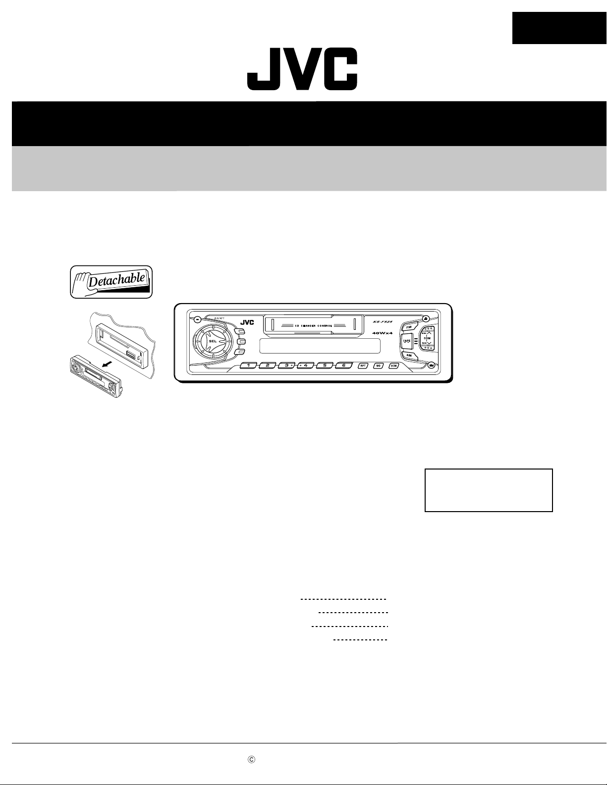
SERVICE MANUAL
DISP
SCAN
LOUD
CASSETTE RECEIVER
KS-F525
KS-F525
LOUD
DISP
SCAN
Contents
Safety precaution
Disassembly method
Adjustment method
Description of major ICs
Multi
Music
Scan
1- 2
1- 3
1-12
1-15~20
Area Suffix
EE ----- Russian Federation
COPYRIGHT 2002 VICTOR COMPANY OF JAPAN, LTD.
No.49708
Feb. 2002
Page 2

KS-F525
Safety precaution
!
Burrs formed during molding may be left over on some parts of the chassis. Therefore,
pay attention to such burrs in the case of preforming repair of this system.
1-2
Page 3
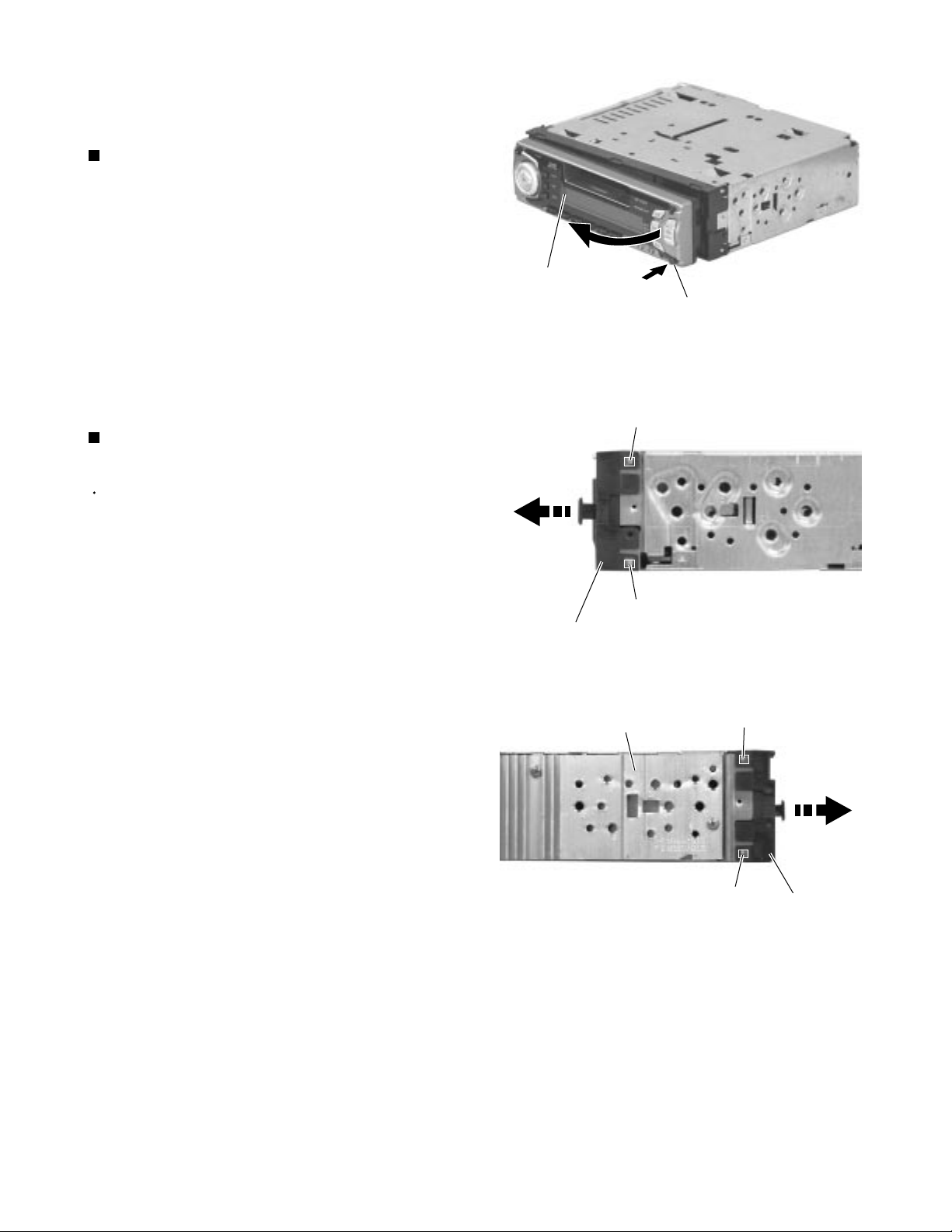
Disassembly method
<Main body>
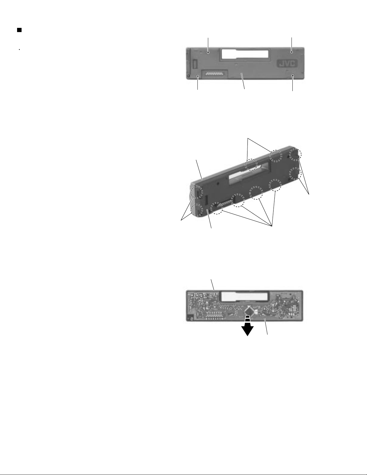
Removing the front panel assembly
(See Fig.1)
1.
Press the eject button in the lower right part of the
front panel. Remove the front panel assembly from
the body.
Removing the front chassis assembly
(See Fig.2 and 3)
KS-F525
Front panel assembly
Eject button
Fig.1
Tab a
Prior to performing the following procedure, remove
the front panel assembly.
1.
Release the four joint tabs a on both sides of the
front chassis assembly and remove the front chassis
assembly toward the front.
Tab a
Front chassis assembly
Heat sink
Fig.2
Tab a
Tab a
Front chassis
assembly
Fig.3
1-3
Page 4
KS-F525
Removing the heat sink (See Fig.4)
1.
Remove the three screws A on the left side of the
body.
Removing the bottom cover
(See Fig.5 and 6)
Prior to performing the following procedure, remove
the front panel assembly, the front chassis assembly
and the heat sink.
1.
Turn over the body and unjoint the five joints b with
the bottom cover and the body using a screwdriver.
Joint b
A
Joints b
Heat sink
Fig.4
Rear panel
Fig.5
A
Bottom cover
Joints b
Joints b
Joints b
Bottom cover
Joint b
Rear panel
Fig.6
1-4
Page 5
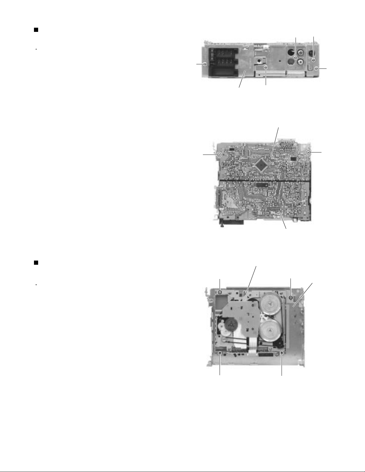
KS-F525
Removing the main board
(See Fig.7 and 8)
Prior to performing the following procedure, remove
the front panel assembly, the front chassis assembly,
the heat sink and the bottom cover.
1.
Remove the screw B, the two screws C and the two
screws D attaching the rear bracket on the back of
the body. Remove the rear panel.
2.
Remove the two screws E attaching the main board
on the bottom of the body. Disconnect connector
CP501 on the main board in the direction of the
arrow.
D
E
Rear panel
C
Fig.7
Main board
B
C
D
E
Removing the cassette mechanism section
(See Fig.9)
Prior to performing the following procedure, remove
the front panel assembly, the front chassis assembly,
the heat sink, the bottom cover and the main board.
1.
Remove the four screws F attaching the cassette
mechanism section on the back of the top chassis.
Fig.8
Cassette mechanism section
F
F
Fig.9
CP501
F
F
Top chassis
1-5
Page 6
KS-F525
Removing the control switch board
(See Fig.10 to 12)
Prior to performing the following procedure, remove
the front panel assembly.
1.
Remove the four screws G attaching the rear cover
on the back of the front panel assembly.
2.
Unjoint the ten joints c with the front panel and the
rear cover.
3.
Remove the control switch board on the back of the
front panel.
G
Front panel
G
Rear cover
Fig.10
Joints c
G
G
Joints c
Joints c
Rear cover
Front panel
Joints c
Fig.11
Control switch board
Fig.12
1-6
Page 7
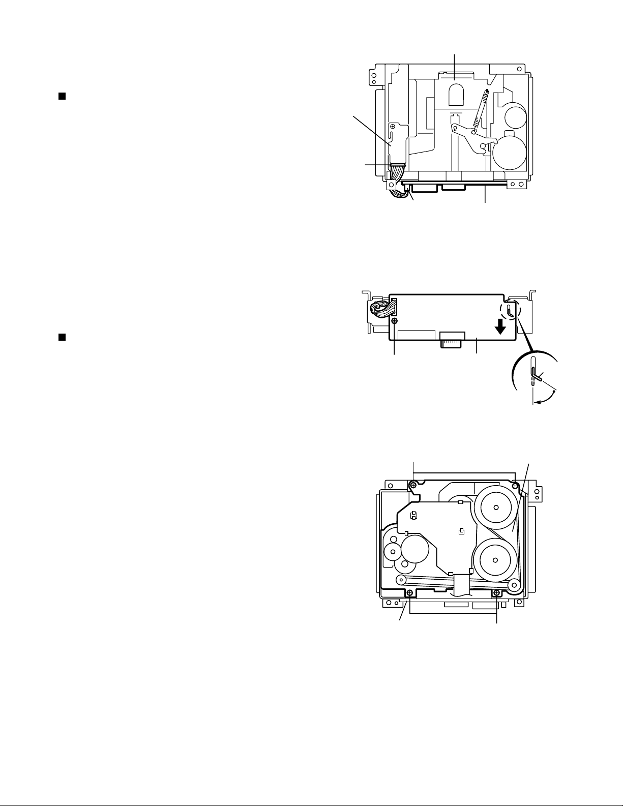
<Removal of the cassette mechanism>
KS-F525
Cassette mechanism ass’y
Removing the head amplifier board.
(See Fig.1 and 2)
1.
For the 6pin wire extending from connector CN402
on the head amplifier board, disconnect it from the
head relay board.
2.
Disconnect the card wire from connector CN403 on
the head amplifier board.
3.
Remove the screw A attaching the head amplifier
board.
4.
Move the tab a as shown in Fig.2 and remove the
head amplifier board while moving it in the direction
of the arrow.
Removing the cassette mechanism
assembly (See Fig.1 to 3)
1.
Disconnect the 6pin wire from connector CN402 and
the card wire from CN403 on the head amplifier
board (Refer to Fig.1 and 2).
Head relay
board
6pin
wire
CN402
A
CN403
CN402
Fig.1
CN403
Head amplifier board
Fig.2
Head amplifier board
Tab a
2.
Remove the four screws B on the bottom of the
cassette mechanism.
Head amplifier board
B
Cassette mechanism ass’y
B
Fig.3
1-7
Page 8

KS-F525
Removing the head relay board
(See Fig.4)
1.
Unsolder the soldering b on the head relay board.
2.
Remove the screw C attaching the head relay board.
3.
Remove the head relay board in the direction of the
arrow while releasing the two joints c.
Removing the load arm (See Fig.5)
1.
Remove the E washer attaching the load arm using
a pincette or something like that and remove the
spring d.
2.
Move the part of the load arm marked upwards to
release it from the axis of rotation. Then rotate the
load arm in the direction of the arrow to remove it
from the cach.
Fig.4
Cach
Load arm
Fig.5
Head relay board
Soldering b
C
E washer
Joint c
Spring d
Removing the sub chassis (See Fig.6)
Prior to performing the following procedure, remove
the head relay board.
1.
Remove the screw D attaching the sub chassis.
2.
Push the tab e in the direction of the arrow to detach
the one side of the sub chassis. Then release the
sub chassis from the tab f.
Removing the cassette holder and the
holder arm in the eject mode
(See Fig.7 and 8)
Prior to performing the following procedure, remove
the head relay board, the load arm and the sub
chassis.
1.
Remove the screw E attaching the reinforce bracket.
2.
Remove the reinforce bracket.
Tab f
Sub chassis
Head relay
board
D
Cassette mecha chassis
Cassette holder
Fig.6
Head relay board
Tab e
Reinforce bracket
E
Reinforce
bracket
tab g
3.
Push the tab g fixing the cassette holder in the
direction of the arrow and open the cassette holder
and the holder arm upward until they stop at an
angle of 45 degrees. Move the two joints h to the
side and remove the cassette holder and the holder
arm from the shaft.
1-8
Joint h
Load arm
Holder arm
Fig.7
Joint h
Page 9

Removing the play head (See Fig.9)
Prior to performing the following procedure, remove
the head relay board and the sub chassis.
1.
Remove the two screws F attaching the play head
(The spring under the play head comes off at the
same time).
Shaft
Joint h
Pinch roller ass’y
Fig.8
Play head
KS-F525
Cassette holder
and holder arm
Joint h
Shaft
Pinch roller ass’y
Removing the pinch roller ass’y
(See Fig.9)
Prior to performing the following procedure, remove
the head relay board and the sub chassis.
1.
Push each tab i in the direction of the arrow and pull
out the pinch rollers on both sides.
Removing the reel disc board
(See Fig.10)
1.
Unsolder the soldering j on the reel disc board.
2.
Push the seven tabs k on the bottom of the cassette
mechanism assembly in the direction of the arrow.
Removing the motor and the sub motor
(See Fig.10 and 11)
Tab i
Tab i
Soldering j
G
Motor
F
Pinch roller ass’y
Fig.9
Reel disc board
Tabs k
Tabs k
G
Tab i
Spring
Tab i
Cassette mechanism ass’y
Flyhwheel
Belt
Fig.10
1.
Unsolder the two soldering l of the motor and the sub
motor.
2.
Release the sub motor from the three tabs m. Push
the sub motor upward and pull out it.
3.
Remove the belt on the bottom of the cassette
mechanism assembly and remove the two screws G
attaching the motor.
ATTENTION:
The motors can be detached before
removing the load arm.
Sub motor
Tab m
Load arm
Soldering j
Tab m
Soldering l
Tab m
Soldering l
Motor
Fig.11
1-9
Page 10

KS-F525
Removing the flywheel
(See Fig.10 and 12)
1.
Prior to performing the following procedure, remove
the head relay board, the load arm, the sub chassis,
the cassette holder, the holder arm and the reel disc
board.
2.
Remove the belt on the bottom of the cassette
mechanism ass’y.
3.
Remove the slit washer attaching the flywheel on the
upper side of the cassette mechanism ass’y and pull
out the flywheel downward. Then remove another
flywheel in the same way.
ATTENTION:
When reassembling, make sure to use
a new slit washer.
Removing the reel disc ass’y( )
(See Fig.12 to 14)
Soldering j
G
Motor
Plate
Reel disc board
G
Slit washer
Tab k
Tab o
Cassette mechanism ass’y
Tab k
Belt
Fig.10
Reel driver
The part n
Tabs o
Flyhwheel
Reel disc
ass’y( )
Push aside
the gear
Prior to performing the following procedure, remove
the head relay board, the load arm, the sub chassis,
the cassette holder and the holder arm.
1.
Disengage the part n inside of the reel driver which
engages with the shaft, using a pincette or
something like that. Then remove the reel driver from
the shaft.
2.
Remove the reel driver spring and the reel table.
The part n
Slit washer
Shaft
Fig.13
The part n
Reel driver
Fig.12
Reel driver
Reel driver spring
Reel disc ass’y( )
1-10
Reel table
Fig.14
Page 11

KS-F525
Removing the reel disc ass’y( )
(See Fig.12 to 15)
ATTENTION:
1.
Release the plate from the three tabs o.
2.
Push aside the gear over the reel table using a
pincette or something like that.
3.
Remove the reel disc ass’y ( ) as with the reel disc
ass’y ( ).
ATTENTION:
Prior to performing the following
procedure, remove the reel disc ( ).
Do not break the front panel tab fitted
to the metal cover.
Push aside the gear and reattach the reel disc Ass’y( ).
Reel disc ass’y( )
Fig.15
1-11
Page 12

KS-F525
Adjustment method
Test Instruments reqired for adjustment
1.Digital osclloscope(100MHz)
2.Frequency Counter meter
3.Electric voltmeter
4.Wow & flutter meter
5.Test Tapes
VT724
VT739
VT712
VT703
6.Torque gauge
Power supply voltage
Load impedance
Line out
For playback frequency measurement
For wow flutter & tape speed measurement
Measuring conditions(Amplifier section)
for DOLBY level measurement
For head azimuth measurement
Cassette type for CTG-N
(mechanism adjustment)
DC14.4V(10.5~16V)
4 (2Speakers connection)
20k
Frequency Range
FM1/FM2 : 87.5 MHz to 108.0 MHz
FM3 : 65 MHz to 74 Hz
AM : (MW) 522 kHz to 1620 kHz
(LW) 144 kHz to 279 kHz
DUMMY LOAD
Exclusive dummy load should be used for AM
and FM dummy load,there is a loss of 6dB
between SSG output and antenna input. The
loss of 6dB need not be considered since
direct reading of figures are applied in this
working standard.
Standard volume position
Balance and Bass,Treble volume .Fader
:Center(Indication"0")
Loudness,Dolby NR,Sound,Cruise:Off
Volume position is about 2V at speaker output with
following conditions.Playback the test tape VT721.
AM mode 999kHz/62dB,INT/400Hz,30%
modulation signal on receiving.
FM mono mode 97.9MHz/66dB,INT/400Hz,22.5kHz
deviation pilot off mono.
FM stereo mode 1kHz,67.5kHz dev. pilot7.5kHz dev.
Output level 0dB(1 V,50 /open terminal).
Arrangement of Adjusting
Cassette Mechanism Section
Capstan motor
Cassette mechanism
(Surface)
Azimuth screw
(Forward side)
Playback head
Tape speed adjust
1-12
Azimuth screw
(Reverse side)
Page 13

KS-F525
Main board
Arrangment of adjusting
Head amplifier board section (Reverse side)
VR402:Rch
(Dolby NR level adj)
R411
VR402
T11
FSMW1093A
B409
R426
C423
R425
D401
R424
IC402
C418
R417
R415
C415
B410
1
B411
R412
R414
R418
21
R413
C417
B404
CJ403
2
B407
C425
C424
R410
Q401
B406
D402
R401
R416
C419
C422
C414
B408
C416
C421
R420
Q403
B403
B413
C413
1
VR401:Rch
(Dolby NR Frequency response adj)
11
C412
1
IC401
31
C411
B405
B412
R423
B402
VR401
C410
CJ401
R408
B401
C409
C405
R407
C406
C408
C402
R406
C407
R403
1
R405
C404
R404
C403
R422
C401
R402
2
Q402
1
Information for using a car audio service jig
1. We're advancing efforts to make our extension cords common for all car audio products.
Please use this type of extension cord as follows.
2. As a U-shape type top cover is employed, this type of extension cord is needed to check operation of the
mechanism assembly after disassembly.
3. Extension cord : EXTKSRT002-18P ( 18 pin extension cord ) For connection between mechanism assembly
and main board assembly.
Check for mechanism driving section such as motor ,etc..
Disassembly method
1. Remove the bottom cover.
2. Remove the front panel assembly.
3. Remove the top cover .
4. Install the front panel.
5. Confirm that current is being carried by connecting
an extension cord jig.
Note
Available to connect to the CP701 connector when installing the front panel.
Extension cord
EXTKSRT002-18P
to Cassette mechanism
Cassette mechanism
Main board
EXTKSRT002-18P
to Main board
Front panel assembly
1-13
Page 14

KS-F525
Item
Head
1.
azimuth
adjustment
Conditions
Test tape:
SCC-1659
VT703(10kHz)
Adjustment and Confirmation methods
Head height adjustment
Adjust the azimuth directly. When you
adjust the height using a mirror tape,
remove the cassette housing from the
mechanism chassis. After installing the
cassette housing, perform the azimuth
adjustment.
Load the SCC-1659 mirror tape. Adjust with
1.
height adjustment screw A and azimuth
adjustment screw B so that line A of the
mirror tape runs in the center between Lch
and Rch in the reverse play mode.
After switching from REV to FWD then to
2.
REV, check that the head position set in
procedure 1 is not changed. (If the position
has shifted, adjust again and check.)
Adjust with azimuth adjustment screw B so
3.
that line B of the mirror tape runs in the
center between Lch and Rch in the forward
play mode.
Head azimuth adjustment
Load VT724 (1kHz) and play it back in
1.
the reverse play mode.
Set the Rch output level to max.
Load VT703 (10kHz) and play it back in
2.
the forward play mode. Adjust the Rch
and Lch output levels to max, with
azimuth adjustment screw B. In this case,
the phase difference should be within 45 .
Engage the reverse mode and adjust the
3.
output level to max, with azimuth
adjustment screw C.
(The phase difference should be 45 or
more.)
When switching between forward and
4.
reverse modes, the difference between
channels should be within 3dB. (Between
FWD L and R, REV L and R.)
S.Values Adjust
A line
Head shield
The head is at low position
during.
B line
Head shield
The head is at High position
during REV.
Output
level:
Maximum
PBHead
FWD Adj B
REV Adj C
(0 ) (45 )
HEIGHT Adj A
phase
2.
3.
1-14
Tape speed
and wow
flutter
confirmation
Play back
frequency
response
confiramation
When VT721 (315Hz) is played back,
5.
the level difference between channels
should be within 1.5dB.
Test tape: VT712
(3kHz)
Test tape: VT724
(1kHz)
VT739
(63Hz / 1kHz / 10kHz)
The tuner section is of an adjustment-freedesign. In case the tuner is in trouble, replace the tuner pack.
Check to see if the reading of the F, counter /
1.
wow flutter meter is within 3015 3045(FWD
/ REV), and less than 0.35% (JIS RMS).
In case of out of specification, adjust the
2.
motor with a built-in volume resistor.
Play test tape VT724, and set the volume
1.
position at 2V.
Play test tape VT739 and confirm.
2.
1kHz / 10kHz: -1 3dB,
1kHz / 63Hz: 0 3dB,
When 10kHz is out of specification, it will be
3.
necessary to read adjust the azimuth.
Tape speed:
3015
3045Hz
Wow
flutter: less
than 0.35%
Speaker out
1kHz / 63Hz
: 0 3db
1kHz / 10kHz
: -1 3db
Built-in volume
resistor
Page 15

Description of major ICs
UPD178018AGC594(IC701) : System controller micon
1.Terminal Layout
24 – 1
25
80
KS-F525
–
40
–
65
41 – 64
2.Description
Pin
Symbol I/O Function
No.
1 KEY0 I Key input 0
2 KEY1 I Key input 1
3 KEY2 I Key input 2
4 LEVEL I Level meter input
5 SM I Signal meter input
6 SQ I Signal quality input
7 LCDCE O Chip enable output to LCD driver
8 LCDDA O Data output to LCD driver
9 LCDSCK O Clock output to LCD driver
10 BUSI/O O J-BUS I/O switch output
11 UNLOCK O PLL unlock output L:unlock H:lock
12 BUSSI I J-BUS data input
13 BUSSO O J-BUS data output
14 BUSSCK O J-BUS clock output
15 - 20 NC - Non connect
21 GNDPORT - GND for port
22 VDDPORT - VDD for port
23 NC - Non connect
24 AFCK O AF check output L:AF check
25 MONO O Monaural ON/OFF output H:Monaural ON
26 FM O Output for FM power supply H:FM Mode
27 SEEK/STOP O Auto seek/Stop output H:Aut seek L:Stop
28 NC I Non connect
29 IFC I FM middle frequency counter input
30 VDDPLL - VDD for PLL
31 OSC I FM/AM oscillation input
32 NC - Non connect
33 GNDPLL - GND for PLL
34 AMEO O AM error out output
35 FMEO O FM error out output
36 IC - Connect to Ground
37 SD/ST I Seek/Stop port H:SD input
Seek/Stop port L:Stereo input
38 STAGE I H:It is CD mode and there is REPEAT
L:Does not exist
39 NC - Non connect
40 MOTOR O Main motor output H:At rotation
41 FF/REW O MS IC sensitivity switch output L:FF/REW
42 F/R O FWD/REV change input H:FWD L:REV
Pin
Symbol I/O Function
No.
43 DOLBY O Dolby NR output H:Dolby NR ON
44 MS IN I Between tunes signal input
H:Between tunes
45 I2CSCK I/O E-VOL IC control clock I/O
46 I2CDAO O E-VOL IC control data output
47 I2CDAI I E-VOL IC control data input
48 REEL I Reel rotation detect signal input
49 SUBMO- O Sub motor output 50 SUBMO+ O Sub motor output +
51 MODE I Mode position detection input H:Non-mode
L:Mode position
52 TAPEIN I Cassette in detect input H:IN L:OUT
53 STBY I Standby detect input H:Eject side
L:Operation side
54-59 NC - Non connect
60 MUTE 2 O L:Mute ON H:Mute OFF
61 POWER O Power supply output H:power ON
62 TEL-MUTE I TEL-MUTE input
63, 64 NC - Non connect
65 ENC1 I Encoder signal input
66 ENC2 I Encoder signal input
67 ON I H:Operation mode L:Power save mode
68 ST
69
70 RDSDA I RDS data input
71 REMOCON I Remocon signal input (Not used)
7
2 DETACH I Detach input It is "L" of 200ms or more and
73 JBUS INT I J-BUS Interruption input
74 REGCPU - Connects GND through the capacitor
75 GND - To ground
76 X2 - Crystal oscillator connection for system
77 X1 - clock oscillation
78 REGOSC - Connects GND through the capacitor
79 VDD - Power supply
80 NC - Non connect
OP
RDSCK
I Stop mode input
I RDS clock input
an operation mode H:power save mode
of 0.1 F
of 0.1 F
1-15
Page 16

KS-F525
BA4905-V3 (IC961) : Regulator
1.Pin layout
12 34 56 78 9101112
2.Block diagram
REGULATOR
EXT
RESET
1 2 3 4 5 6 7 8 9 10 11 12
RESET COMP VDD 5.7V CD 8V VCC AJ
EXT ACC AUDIO 9V CTRL ILM 10V GND
3.Pin function
Pin no. Symbol Function
1
2
RESET
EXT output
If VDD voltage becomes 4V or less.RESET output becomes low level.
This output voltage is approximately 0.5V lower than VCC. and max
output current is 300mA.
3
COMP output
A voltage supply for ACC block. This output voltage is approximately
0.7V lower than VDD'S. The max output current is 100mA.
4
5
ACC
VDD output
Control of the COMP output by inputting voltage.
This output voltage is 5.7V, and max output current is 100mA.
This voltage supply is for microcomputer. Whenever back up voltage
supply is connected, the output keeps on running.
6
AUDIO output
This output voltage is 9.0v, and max output current is 500mA.
This voltage supply for AUDIO.
7
CD output
This output voltage is 8.0V, and max output current is 1A.
This voltage supply for CD.
8
9
10
CTRL
VCC
ILM output
Output selector of CD. AUDIO, ILM and EXT.
To be connected with the BACK UP of car.
This output voltage is 10V, and max output current is 500mA.
Output voltage is adjustable.
11
AJ
Putting a resistance between ILM and AJ or between AJ and GND
makes ILM output voltage adjustable.
12
GND
Ground.
Overvoltage
protection circuit
37K
5K
1-16
Page 17

CXA2559Q(IC401):Playback equalizer amplifier with music sensor
30
29
28
27
26
1.Pin layout
10
3.Pin function
2.Blockdiagram
31
1
30
21
32
33
34
35
36
37
38
39
40
45k
7k/12k
300k
300k
7k/12k
1
30k
30k
-
+
F2
F1
+
-
2
100k
X1
X1
100k
3
4
25
T2
BIAS
MUTE
TAPE EQ
FWD/RVS
LPF
T1
5
6
Vcc
KS-F525
24
23
22
21
24dB
-
+
MS MODE
+
-
F3
+
7
DET
-
24dB
8
9
MS ON/
OFF
10
20
19
18
17
16
15
14
13
12
11
Pin No.
1
2
3
4
5
6
7
8,9
10
11
12
13
14
15,16
17
18
19
20
21
22,23
24
25
26
27
28
29
30
31
32
33
34
35
36
37
38
39
40
Symbol
PBTC1
PBOUT1
OUTREF1
TAPEIN1
Vcc
NC
LINEOUT1
NC
MSLPF
G2FB
GI1FB
MSTC
MSOUT
NC
MUTESW
TAPESW
DRSW
MSMODE
MSSW
NC
LINEOUT2
DIREF
GND
TAPEIN2
OUTREF2
PBOUT2
PBTC2
PBFB2
PNRIN2
PBGND
PBFIN2
VCT
PBREF
PBFIN1
PBGND
PBRIN1
PBFB1
I/O
Function
-
Terminal of capacity of reproduction equalizer reproduction
O
Equalizer output terminal
O
Output standard terminal
I
Tape input terminal
-
Power supply terminal
-
Non connection
O
Line-out output terminal
-
Non connection
-
Detection LPF terminal between tunes
-
Detection level set terminal between tunes
-
Detection level set terminal between tunes
-
Time constant connection terminal for the detection between tunes
O
Detection output terminal between tunes
-
Non connection
I
Mute function control terminal
I
Reproduction equalizer control terminal
I
Head change control terminal
I
Detection mode control terminal between tunes
I
Detection function control terminal between tunes
-
Non connection
O
Line-out output terminal
-
Resistance connection terminal for standard current setting
-
Earth terminal
I
Tape input terminal
O
Output standard terminal
O
Reproduction equalizer output terminal
-
Terminal of capacity of reproduction equalizer
I
Reproduction equalizer return terminal
I
Reproduction equalizer input terminal
-
Reproduction equalizer system earth terminal
I
Reproduction equalizer input terminal
O
Middle point terminal
O
Reproduction equalizer standard terminal
I
Reproduction equalizer input terminal
-
Reproduction equalizer system earth terminal
I
Reproduction equalizer input terminal
I
Reproduction equalizer return terminal
1-17
Page 18

KS-F525
HA13158A (IC941) : Power amp
1. Pin layout
1 ~ 23
2. Block diagram
2
STBY
IN1
1
14 18 6
INVCC
INPUTBUFFER1
PVCC1PVCC2
AMP1
+
3
4
-
5
IN2
IN3
IN4
11
13
23
10
MUTE
INPUTBUFFER2
INPUTBUFFER3
INPUTBUFFER4
PROTECTOR (ASO
SURGE, TSD)
12 22
LB1641 (IC402) : DC motor driver
AMP2
AMP3
AMP4
TA B
+
7
8
-
9
15
+
16
-
17
19
+
20
-
21
1. Pin layout
1-18
1 2 3 4 5 6 7 8 9
GND OUT1 P1
VZ IN1 IN2
VCC1
VCC2 P2
2. Pin function
10
OUT2
Input Output
IN1 IN2 OUT1 OUT2
0 0 0 0
1 0 1 0
0 1 0 1
1 1 0 0
Mode
Brake
CLOCKWISE
COUNTER-CLOCKWISE
Brake
Page 19

LC75823W (IC651) : LCD driver
1. Pin Layout & Symbol
KS-F525
S1
S2
S3
S4
S5
S6
S7
S8
S9
S10
S11
S12
S13
S14
S15
S16
DICLCE
64 63 62 61 60 59 58 57 56 55 54 53 52 51 50 49
1
2
3
4
5
6
7
8
9
10
11
12
13
14
15
16
17 18 19 20 21 22 23 24 25 26 27 28 29 30 31 32
S17
S18
S19
OSC
S20
Vss
S21
VDD2
VDD1
S22
S23
INH
S24
VDD
S25
COM3
COM2
S26
S27
COM1
S52
S28
S29
S51
S30
S50
S31
S49
48
47
46
45
44
43
42
41
40
39
38
37
36
35
34
33
S32
S48
S47
S46
S45
S44
S43
S42
S41
S40
S39
S38
S37
S36
S35
S34
S33
2. Pin Function
Pin No.
1 to 52
53 to 55
COM1 to COM3
56
57
58
59
60
61
62
63
Symbol
S1 to S52
VDD
INH
VDD1
VDD2
Vss
OSC
CE
CL
I/O
O
Segment output pins used to display data transferred
Function
by serial data input.
O
Common driver output pins. The frame frequency is given
by : t0=(fosc/384)Hz.
--
Power supply connection. Provide a voltage of between
4.5 and 6.0V.
I
Display turning off input pin.
INT="L" (Vss) ----- off (S1 to S52, COM1 to COM3="L"
INT="H" (VDD)----- on
Serial data can be transferred in display off mode.
I
Used for applying the LCD drive 2/3 bias voltage
externally.
Must be connected to VDD2 when a 1/2 bias drive scheme
is used.
I
Used for applying the LCD drive 1/3 bias voltage
externally.
Must be connected to VDD1 when a 1/2 bias drive scheme
is used.
--
Power supply connection. Connect to GND.
I/O
Oscillator connection.
An oscillator circuit is formed by connecting an external
resistor and capacitor at this pin.
Serial data CE : Chip enable
interface connection
I
to the controller. CL : Sync clock
64
DI
DI : Transfer data
1-19
Page 20

KS-F525
TEA6320T-X (IC161) : E.volume
1.Pin layout
2.Block diagram
10 8 9 7 6
5
12
SDA
1
GND
2
OUTLR
OUTLF
MUTE
TL
B2L
B1L
IVL
ILL
QSL
IDL
ICL
IMD
IBL
IAL
3
4
5
6
7
8
9
10
11
12
13
14
15
16
3.Pin functions
Pin
Symbol
No.
SDA
1
SCL
32
VCC
31
OUTRR
30
OUTRF
29
TR
28
B2R
27
B1R
26
IVR
25
ILR
24
QSR
23
IDR
22
Vref
21
ICR
CD-CH
TAPE
TUNER
20
19
18
17
CAP
IBR
IAR
I/O
Serial data input/output.
I/O
MUTE
21
31
2
19
16
15
13
11
14
22
20
18
17
Functions Functions
POWER
SUPPLY
SOURCE
SELECTOR
23 25 24 26 27 28
VOLUME 1
+20 to -31 dB
LOUDNESS
LEFT
VOLUME 1
+20 to -31 dB
LOUDNESS
RIGHT
Pin
No.
17
Symbol
IAR
BASS
LEFT
+15 dB
LOGIC
BASS
RIGHT
+15 dB
I/O
I
Input A right source.
TREBLE
LEFT
+12 dB
TREBLE
RIGHT
+12 dB
FUNCTION
ZERO CROSS
DETECTOR
VOLUME 2
0 to 55 dB
BALANCE
FENDER REAR
VOLUME 2
0 to 55 dB
BALANCE
FENDER FRONT
HC BUS
REC
VOLUME 2
0 to -55dB
BALANCE
FENDER FRONT
VOLUME 2
0 to -55dB
BALANCE
FENDER REAR
3
4
32
1
29
30
2
3
4
5
6
7
8
9
10
11
12
13
14
15
16
GND
OUTLR
OUTLF
TL
B2L
B1L
IVL
ILL
QSL
IDL
MUTE
ICL
IMO
IBL
IAL
Ground.
-
output left rear.
O
output left front.
O
Treble control capacitor left channel or
I
input from an external equalizer.
Bass control capacitor left channel or
-
output to an external equalizer.
Bass control capacitor left channel.
-
Input volume 1. left control part.
I
Input loudness. left control part.
I
Output source selector. left channel.
O
Not used
-
Not used
-
Input C left source.
I
Not used
-
Input B left source.
I
Input A left source.
I
18
19
20
21
22
23
24
25
26
27
28
29
30
31
32
IBR
CAP
ICR
Vref
IDR
QSR
ILR
IVR
B1R
B2R
TR
OUTRF
OUTRR
Vcc
SCL
I
Input B right source.
-
Electronic filtering for supply.
I
Input C right source.
-
Reference voltage (0.5Vcc)
-
Not used
O
Output source selector right channel.
I
Input loudness right channel.
I
Input volume 1. right control part.
-
Bass control capacitor right channel
Bass control capacitor right channel or
O
output to an external equalizer.
Treble control capacitor right channel or
I
input from an external equalizer.
O
Output right front.
O
Output right rear.
-
Supply voltage.
I
Serial clock input.
1-20
Page 21

< MEMO >
KS-F525
1-21
Page 22

KS-F525
VICTOR COMPANY OF JAPAN, LIMITED
MOBILE ELECTRONICS DIVISION
PERSONAL & MOBILE NETWORK BUSINESS UNIT. 10-1,1Chome,Ohwatari-machi,Maebashi-city,371-8543,Japan
(No.49708)
200202
 Loading...