

Page 1
49813200302
KS-F383R,KS-F380R
SERVICE MANUAL
CASSETTE RECEIVER
KS-F383R,KS-F380R
Area Suffix
E ---- Continental Europe
EX -------- Central Europe
F
LO
UD
D
ISP
Model
KS-F383R
KS-F380R
SEL
O
Illumination color
Amber
Green
M
A
M
SS
M
TP
PTY
SCMM
TABLE OF CONTENTS
1 Important Safety Precautions . . . . . . . . . . . . . . . . . . . . . . . . . . . . . . . . . . . . . . . . . . . . . . . . . . . . . . . . . . . 1-2
2 Disassembly method . . . . . . . . . . . . . . . . . . . . . . . . . . . . . . . . . . . . . . . . . . . . . . . . . . . . . . . . . . . . . . . . . . 1-3
3 Adjustment method. . . . . . . . . . . . . . . . . . . . . . . . . . . . . . . . . . . . . . . . . . . . . . . . . . . . . . . . . . . . . . . . . . . 1-12
4 Description of major ICs. . . . . . . . . . . . . . . . . . . . . . . . . . . . . . . . . . . . . . . . . . . . . . . . . . . . . . . . . . . . . . . 1-16
COPYRIGHT © 2003 VICTOR COMPANY OF JAPAN, LTD.
No.49813
2003/03
Page 2

KS-F383R,KS-F380R
1.1 Safety Precautions
SECTION 1
Important Safety Precautions
!
Burrs formed during molding may be left over on some parts of the chassis. Therefore,
pay attention to such burrs in the case of preforming repair of this system.
1-2 (No.49813)
Page 3
SECTION 2
Disassembly method
2.1 Main body
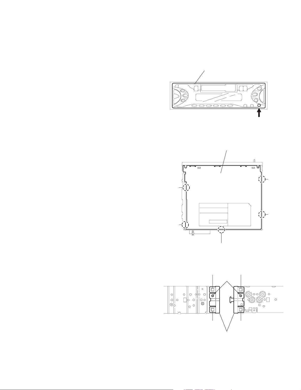
2.1.1 Removing the front panel assembly (See Fig.1)
(1) P ress the release button and remove the front panel as-
sembly.
2.1.2 Removing the bottom cover (See Fig.2)
• Prior to performing the following procedure, remove the front
panel assembly.
(1) Turn the body upside down.
(2) Insert a screwdriver under the joints to release the two
joints a on the left si de, the two joints b on the right side and
the joint c on the back of the body, then remove the bottom
cover from the body.
CAUTION:
When releasing the joint c using a screwdriver, do not
damage the main board.
KS-F383R,KS-F380R
Front panel assembly
Release button
Fig.1
Bottom cover
Joint b
Joint a
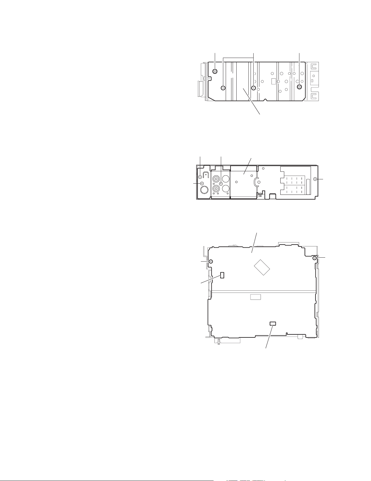
2.1.3 Removing the front chassis (See Fig.3)
• Prior to performing the following procedure, remove the front
panel assembly and bottom cover.
(1) Remove the screw A on each side of the body.
(2) Release the two joints d and two joints e on the sides, then
remove the front chassis toward the front.
Joint a
Joint c
Fig.2
Joint d Joint e
A
Joint d
Front chassis
Fig.3
Joint e
Joint b
(No.49813)1-3
Page 4
KS-F383R,KS-F380R
2.1.4 Removing the heat sink (See Fig.4)
• Prior to performing the following procedure, remove the front
panel assembly.
(1) Remove the two screws B and two screws C attaching the
heat sink on the left side of the body, and remove the heat
sink.
2.1.5 Removing the rear panel (See Fig.5 )
• Prior to performing the following procedure, remove the front
panel assembly and bottom cover.
(1) Remove the two screws D, screws E and screw F attaching
the rear panel on the back of the body.
CB C
Heat sink
Fig.4
FD
Rear panel
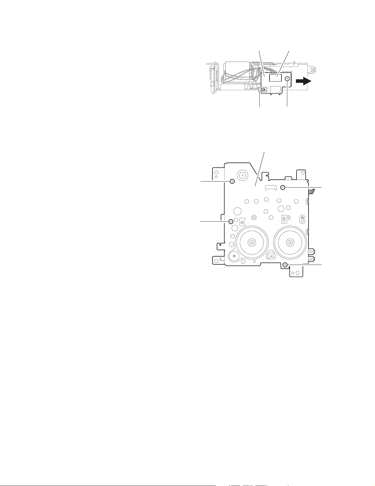
2.1.6 Removing the main board (See Fig.6)
• Prior to performing the following procedure, remove the front
panel assembly, bottom cover, front chassis, heat sink and
rear panel.
(1) Remove the two screws G attaching the main board on the
top chassis.
(2) Di sconnect the two connectors CN901 and CN9 02 on the
main board from the cassette mechanism assembly.
E
G
CN902
D
Fig.5
Main board
G
CN901
Fig.6
1-4 (No.49813)
Page 5
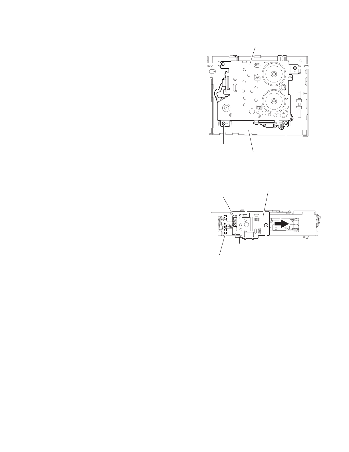
2.1.7 Removing the cassette mechanism assembly
(See Fig.7)
• Prior to performing the following procedure, remove the front
panel assembly, bottom cover, front chassis, heat sink, rear
panel and main board.
(1) Remove th e four screws H attaching the cassette mecha-
nism assembly on the top chassis.
H
KS-F383R,KS-F380R
Cassette mechanism assembly
H
2.1.8 Removing the head amplifier board
(See Fig.8)
• Prior to performing the following procedure, remove the front
panel assembly, bottom cover, front chassis, heat sink, rear
panel, main board and cassette mechanism assembly.
(1) Disconnect the wire from CJ901 on the head amplifier
board.
(2) Remove the screw J attaching the head amplifier board.
(3) Move the head amplifier board in the direction of the arrow
to release the two joints f, the head amplifier board can be
removed.
H
CJ901
Joint f
To head relay board
H
Top chassis
Fig.7
Head amplifier board
Joint f
J
Fig.8
(No.49813)1-5
Page 6
KS-F383R,KS-F380R
2.1.9 Removing the relay board (See Fig.9)
• Prior to performing the following procedure, remove the front
panel assembly, bottom cover, front chassis, heat sink, rear
panel, main board and cassette mechanism assembly.
(1) Di sco nnect the wire from CP722 on the relay board.
(2) Remove the screw K attaching the relay board.
(3) Move the relay board in the direction of the arrow to release
the joint g, the relay board can be removed.
Relay board
CP722
2.1.10 Removing the mecha br acket (See Fig.10)
• Prior to performing the following procedure, remove the front
panel assembly, bottom cover, front chassis, heat sink, rear
panel, main board, cassette mechanism assembly, head amplifier board and relay board.
(1) Remove the four screws L attaching the mecha bracket.
Joint g
Fig.9
Mecha bracket
K
L
L
L
L
Fig.10
1-6 (No.49813)
Page 7
2.1.11 Removing the switch (LCD & key) board
(See Fig.11~13)
• Prior to performing the following procedure, remove the front
panel assembly.
(1) Remove the four screws M attaching the rear cover on the
back of the front panel assembly.
(2) Release the eleven joints h, the front panel and the rear
cover become separate.
(3) Remove the switch board from the rear cover.
KS-F383R,KS-F380R
M
M
M M
Fig.11
Joint h
Joint hJoint h
Joint h
Fig.12
Switch (LCD & Key) board
Fig.13
(No.49813)1-7
Page 8
KS-F383R,KS-F380R
2.2 Cassette mechanism assembly
• Prior to performing the following procedures, remove the head
amplifier board, the relay board and the mechanism bracket.
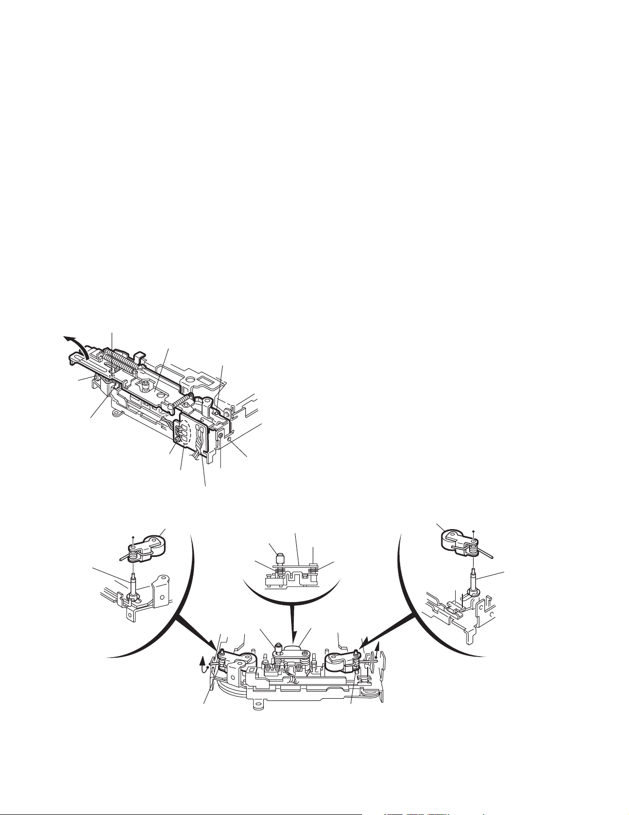
2.2.1 Removing the direction switch board (See Fig.1)
(1) Uns older the three wires a on the direction switch board.
(2) Remove the one screw A attaching the direction switch
board.
2.2.2 Removing the FF / REW lever assembly (See Fig.1)
(1) Remove the screw B attaching the FF / REW lever assem-
bly on the back of the cassette mechanism assembly.
(2) Remove the screw C on the upper side of the FF / REW
lever assembly.
(3) Lift and pull forward the FF / REW lever assembly to disen-
gage the joints b, c, d and e.
2.2.3 Reattaching the FF / REW lever assembly (See Fig.1)
(1) Reattach the FF / REW lever assembly to the joint c on the
back of the chassis.
(2) Reattach the pinch-roller shaft e, the change lever d and
the return link e to the chassis.
C
FF / REW lever assembly
Joint c
2.2.4 Removing the playback head (See Fig.2)
• Prior to performing the following procedure, remove the direc-
tion switch board and the FF / REW lever assembly.
(1) Remove the screw D attaching the playback head.
(2) Remove the C washer and pull out the FF roller.
(3) Remove the S support plate, the A arm spring (a) and (b),
the playback head.
ATTENTION:
The A arm spring (a) differs from the A arm spring (b).
2.2.5 Removing the pinch-roller (R) and (F) assembly (See Fig.2)
• Prior to performing the following procedure, remove the direc-
tion switch board and the FF / REW lever assembly.
(1) Re mov e the P arm spring (f) in the pinch-roller (F) assem-
bly from the chassis.
(2) Remove the P arm spring (r) in the pinch-roller (R) assem-
bly from the chassis.
(3) Draw out the pinch roller (F) and (R) assembly from the
shaft.
ATTENTION:
The P arm spring (f) differs from the P arm spring (r).
ATTENTION:
The pinch roller (F) assembly differs from the pinch roller (R)
assembly.
Joint e
Joint d
A
Soldering a
Direction switch board
Fig.1
Pinch-roller (R) assembly
Shaft
Remove the P arm spring (r)
from the chassis.
Joint b
B
C washer
A arm spring (b)
FF roller
S support plate
D
Playback head
Pinch-roller (F) assembly
A arm spring (a)
Shaft
Remove the P arm spring (f)
from the chassis.
1-8 (No.49813)
P arm spring (r)
P arm spring (f)
Fig.2
Page 9

KS-F383R,KS-F380R
2.2.6 Removing the cassette hanger / cassette holder (See Fig.3)
• Prior to performing the following procedure, remove the FF /
REW lever assembly.
(1) From the rear of the unit, bend the two tabs f outwards and
disengage the two joints g in the direction of the arrow.
(2) P ush the eject lever and remove the cassette holder from
the playback head. Disengage the two joints h of the cassette hanger / cassette holder and the eject lever in the direction of the arrow.
(3) Lift the cassette hanger / cassette holder and disengage
the joint i of the return link and the eject lever.
2.2.7 Removing the reel disc assembly (See Fig.4)
• Prior to performing the following procedure, remove the FF /
REW lever assembly and the cassette hanger / cassette holder.
(1) Remove the C washer and pull out reel disc assembly.
ATTENTION:
Replace with a new C washer when reattaching.
Joint g
Cassette holder
Cassette hanger
Chassis
Tab f
Tab f
C washer
Return link
Joint i
Eject lever
Joint h
Joint h
Joint g
Fig.3
2.2.8 Removing the motor assembly (See Fig.5)
(1) Unsolder the two wires j on the motor assembly.
(2) Turn over the cassette mechanism assembly and remove
the main belt and the sub-belt from the motor pulley.
ATTENTION:
The main belt can now be removed.
(3) Remove the two screws G attaching the motor assembly.
C washer
Flywheel (BF)
Fig.4
Main-belt
E
Reel disc assembly
Motor assembly
Sub-belt
G
E
Motor pulley
G
Soldering j
Flywheel (BR)
Reel base assembly
E
Fig.5
F
(No.49813)1-9
Page 10

KS-F383R,KS-F380R
2.2.9 Removing the Flywheel (BF) and (BR) assembly (See Fig.4 and 5)
• Prior to performing the following procedure, remove the cas-
sette hanger / cassette holder.
(1) From the upper side of the cassette mechanism assembly,
remove the C washer from each shaft of the flywheel (BF)
and (BR).
(2) Turn o ver the cassette mechanism a ssembly and remove
the main belt. Pull out the flywheel (BF) and (BR) downward respectively.
C washer
Reel disc assembly
C washer
Fig.4
Main-belt
Motor assembly
2.2.10 Removing the reel ba se assembly (See Fig.5 and 6)
(1) Raise the part k of the reel base assembly slightly and re-
move the selector link (B) on the front side of the cassette
mechanism assembly by turning it as shown in Fig.6.
(2) Remove the three screws E and the one screw F on the
underside of the cassette mechanism assembly.
ATTENTION:
The reel base assembly is not repairable. Handle with care.
Pinch-roller (R) assembly
k
Selector link (B).
Turn the selector link (B).
Fig.6
Inside of the reel base assembly
Flywheel (BF)
Flywheel (BR)
Sub-belt
E
Reel base assembly
E
Fig.5
G
E
F
Motor pulley
G
Soldering j
Fig.7
1-10 (No.49813)
Page 11

KS-F383R,KS-F380R
2.2.11 Removing the mute switch board (See Fig.8)
(1) Unsolder the two wires l on the mute switch board on the
back of the cassette mechanism assembly.
(2) Remove the screw H attaching the mute switch board.
2.2.12 Removing the power switch (See Fig.9)
• Prior to performing the following procedure, remove the motor
assembly.
(1) Unsol der the two wires m on the power switch on the side
of the cassette mechanism assembly.
(2) Remove the screw I attach ing the power switch.
Cassette mechanism assembly
Soldering l
H
Fig.8
Soldering m
I
Cassette mechanism assembly
Power switch
Fig.9
Rower switch
Motor assembly
Mute switch board
(No.49813)1-11
Page 12

KS-F383R,KS-F380R
SECTION 3
Adjustment method
Test instruments reqired for adjustment Standard volume position
1. Digital oscilloscoe(100MHz)
2. Frequency counter meter
3. Electric voltmeter
4. Wow & flutter meter
5. Test tapes
VT724.......................for DOLBY level measurement
VT739............For playback frequency measurement
VT712....For wow flutter & tape speed measurement
VT703.....................For head azimuth measurement
6. Torque gauge...................Cassette type for CTG-N
(Mechanism adjustment)
Measuring conditions(Amplifier section)
Balance and Bass, Treble volume, Fader
:Center(Indication"0")
Loudness, Dolby NR, Sound, Cruise: Off
Volume position is about 2V at speaker output with
following conditions, Playback the test tape VT721.
AM mode 999kHz/62dB, INT/400Hz,30%
modulation signal on recieving.
FM mono mode 97.9MHz/66dB, INT/400Hz,
22.5kHz deviation pilot off mono
FM stereo mode 1kHz, 67.5kHz dev.pilot 7.5kHz dev
Output level 0dB(1 V,50 /open terminal)
Power supply voltage.............. DC14.4V(11V - 16V allowance)
Load impedance............ 4 (4 to 8 allowance)
Line out level/Impedance..............1.0V/20k load (250 nWb/m)
Frequency band
Band
FM: 87.5 MHz to 108.0 MHz
AM : (MW) 522 kHz to 1620 kHz
(LW) 144 kHz to 279 kHz
1-12 (No.49813)
Page 13

KS-F383R,KS-F380R
Information for using a car audio service jig
1. For 1995 and 1996, we're advancing efforts to make our extension cords common for all car audio products.
Please use this type of extension cord as follows.
2. As a U-shape type top cover is employed, this type of extension cord is needed to check operation of the
mechanism assembly after disassembly.
3. Extension cord : EXTKSRT002-6P ( 6 pin extension cord ) For connection between mechanism assembly
and main board.
4. Check for mechanism driving section such as motor ,etc..
Disassembly method
1. Remove the front panel assembly.
2. Remove the bottom cover.
3. Remove the front chassis.
4. Remove the two screws D of the rear panel. (Refer to Disassembly method.)
5. Remove the heat sink.
6. Reattach the heat sink with two screws B. (Refer to Disassembly method.)
7. Install the front chassis and front panel assmbly.
8. Confirm that current is being carried by connecting an extension cord jig.
Note
Available to connect to the CJ701 connector when installing the front panel.
CAUTION :
Be sure to attach a heat sink on the power amplifier IC of a main board when supplying the power.
If voltage is applied without attaching the heat sink, the power amplifier IC will be destroyed by heat.
Cassette mechanism
EXTKSRT002-6P
Extension cord
: EXTKSRT002-6P
Main board
Front panel assembly
(No.49813)1-13
Page 14

KS-F383R,KS-F380R
Arrangement of adjusting & test points
Cassette mechanism
(Surface)
Motor assembly
Tape speed adjust
Playback head
Azimuth screw
Head section view
Head azimuth screw
Playback head
Height adjusting screw
c
Fixed screw
Height adjusting screw
a
1-14 (No.49813)
Height adjusting screw
b
Page 15

Mechanism adjustment section
Item Adjusting & Confirmation Methods Adjust Std. Value
Head azimuth
1.
"Head Height Adjustment"
Note
Adjust the azimuth directly. When you adjust the height using a mirror tape, remove the cassette housing from the
mechanism chassis.
After installing the cassette housing, perform the azimuth
adjustment.
Head shield
KS-F383R,KS-F380R
A Line
1. Load the mirror tape (SCC-1659). Adjust with height
adjustment screw (a) and azimuth adjustment screw (b) so
that line "A" of the mirror tape runs in the center between
Lch and Rch in the reverse play mode.
2. After switching from REV to FWD then to REV, check that
the head position set in procedure "1" is not changed.
*If the position has shifted, adjust again and check.
3. Adjust the azimuth screw (b) so that line "B" of the mirror
tape runs in the center between Lch and Rch in the forward
play mode.
"Head Azimuth Adjustment"
1. Load the test tape (VT724: 1kHz) and play it back in the
reverse play mode. set the Rch output level to maximum.
2. Load the test tape (VT703: 10kHz) and play it back in the
forward play mode. Adjust the Rch and Lch output levels
to maximum, with azimuth adjustment screw (b).
In this case, the phase difference should be within 45°.
3. Engage the reverse mode and adjust the output level to
maximum, with azimuth adjustment screw (c).
*The phase difference should be 45° or more.
4. When switching between forward and reverse modes, the
difference between channels should be within 3dB.
*Between FWD Lch and Rch, REV Lch and Rch.
5. When the test tape (VT721: 315Hz) is played back, the
level difference between channels should be within 1.5dB.
The head is at low position
during FWD.
B Line
Head shield
The head is at height position
during REV.
Head azimuth
screw
screw (c)
screw (b)
0
Phase
Fixed screw
screw (a)
45
2.Tape Speed
and Wow &
Flutter
3.Playback
Frequency
response
1. Check to see if the reading of the frequency counter & Wow
flutter meter is within 2940-3090 Hz (FWD/REV), and less
than 0.35% (JIS RMS).
2. In case of out of specification, adjust the motor with a built in volume resistor
1. Play the test tape (VT724: 1kHz) back and set the volume
position at 2V
2. Play the test tape (VT739) back and confirm 0 ± 3dB at1kHz/
8kHz and -4+2dB at 1kHz/125Hz.
3. When 8kHz is out of specification, it will be necessary to
readjust the azimuth.
Built-in
volume resistor
Tape Speed
2940-3090Hz
Wow&Flutter
Less than
0.35%
(JIS RMS)
Speaker out
1kHz/8kHz
: 0dB_}3dB,
125Hz/1kHz
: -4dB+2dB,
(No.49813)1-15
Page 16

KS-F383R,KS-F380R
4.1 AN80T05LF (IC961) : Regulator
• Pin layout & Block diagram
Reference Voltage
Thermal
Protection
SECTION 4
Description of major ICs
ASO & Peak
Current Protection
Pre
Drive
Pre
Drive
AMP
Out
AMP
Out
Pre
Drive
123456789101112
ILL
MODE2 MODE1 STB VDD
10V
5.6V
AMP VCC ANT COM
• Pin function
Pin No. Symbol Function
1 ILL 10V power supply for illumination.
2 MODE2 When 5V is input, becomes AM. and the antenna output is turned on.
3 MODE1 When 5V is input, becomes AM. and the output of FM is switched.
4 STB When 5V is input, outputs to ILL, COM, and AMP. It is 0V usually.
5 VDD 5.6V power supply.
6 AMP Power supply supp ly to remote amplifier
7 VCC Back up. connects with ACC with it.
8 ANT Power supply supply to auto antenna.
9 COM 8.7V power supply.
10 AM The power supply of 8.7V to AM.
11 FM The power supply of 8.7V to FM.
12 GND Ground
Pre
Drive
8.7VAM8.7VFM8.7V
Pre
Drive
GND
1-16 (No.49813)
Page 17

4.2 LC75823W (IC651) : LCD driver
• Pin Layout
KS-F383R,KS-F380R
DICLCE
OSC
Vss
VDD2
VDD1
INH
VDD
COM3
COM2
COM1
S52
S51
S50
S49
64 63 62 61 60 59 58 57 56 55 54 53 52 51 50 49
1
S1
S2
S3
S4
S5
S6
S7
S8
S9
S10
S11
S12
S13
S14
S15
S16
2
3
4
5
6
7
8
9
10
11
12
13
14
15
16
48
47
46
45
44
43
42
41
40
39
38
37
36
35
34
33
S48
S47
S46
S45
S44
S43
S42
S41
S40
S39
S38
S37
S36
S35
S34
S33
17 18 19 20 21 22 23 24 25 26 27 28 29 30 31 32
S17
S18
S19
S20
S21
S22
S23
S24
S25
S26
S27
S28
S29
S30
S31
S32
• Pin function
Pin No. Symbol I/O Functions
1 to 52 S1 to S52 O Segment output pins used to display data transferred by serial data input.
53 to 55 COM1 to COM3 O Common driver output pins. The frame frequency is given by : t0 =(fosc/384)Hz.
56 VDD -- Power supply connection. Provide a voltage of between 4.5 and 6.0V.
57 INH
58 VDD1 I Used for applying the LCD drive 2/3 bias voltage externally.
59 VDD2 I Used for applying the LCD drive 1/3 bias voltage externally.
60 Vss -- Power supply connection . Connect to GND.
61 OSC I/O Oscillator connection.
62 CE I Serial data interface connection to the controller. CE : Chip enable
63 CL I Serial data interface connection to the controller. CL : Sync clock
64 DI I Serial data interface connection to the controller. DI : Transfer data
I Display turning off input pin.
INT="L" (Vss) ----- off (S1 to S52, COM1 to COM3="L"
="H" (VDD)----- on
INT
Serial data can be transferred in display off mode.
Must be connected to VDD2 when a 1/2 bias drive scheme is used.
Must be connected to VDD1 when a 1/2 bias drive scheme is used.
An oscillator circuit is formed by connecting an external resistor and capacitor at this pin.
(No.49813)1-17
Page 18

KS-F383R,KS-F380R
4.3 LA4743K (IC941) : Power amp.
• Block diagram
IN 1
TAB
IN 2
+
0.22 F
+
0.22 F
11
1
12
Vcc 1/2 Vcc 3/4
6 20
-
+
Protective
circuit
-
+
2200 F 0.022 F
+
9
7
+
OUT 1+
OUT 1-
PWR GND1
8
+
OUT 2+
5
-
OUT 2-
3
PWR GND2
2
ST BY
R.F
47 F
IN 3
PRE GND
IN 4
+5V
ST ON
+
0.22 F
N.C
+
0.22 F
4
Stand by
Switch
Mute
10
+
Ripple
Filter
Mute
22
circuit
3.3 F
+
15
-
+
-
17
19
10K
+
OUT 3+
OUT 3-
Low Level
Mute ON
25
18
21
23
PWR GND3
OUT 4+
OUT 4-
13
14
Protective
circuit
-
+
+
-
ON TIME C
1-18 (No.49813)
22 F
Muting &
16
+
ON Time Control
Circuit
PWR GND4
24
Page 19

•Pin layout
TAB
GND
FR-
STDBY
FR+
VP1
RR-
GND
RR+
RIPPLE
INRF
INRR
SGND
FLIN
RLIN
DNTIME
RL+
GND
RL-
VP3
FL+
MUTE
FL-
GND
NC
• Pin function
Pin No. Symbol Function
1 TAB Header of IC
2 GND Power GND
3 FR- Outpur(-) for front Rch
4 STDBY Stand by input
5 FR+ Output (+) for front Rch
6 VP1 Power input
7 RR- Output (-) for rear Rch
8 GND Power GND
9 RR+ Output (+) for rear Rch
10 RIPPLE Ripple filter
11 RRIN Rear Rch input
12 FRIN Front Rch input
13 SGND Signal GND
14 FLIN Front Lch input
15 RLIN Rear Lch input
16 ONTIME Power on time control
17 RL+ Output (+) for rear Lch
18 GND Power GND
19 RL- Output (-) for rear Lch
20 VP3 Power input
21 FL+ Output (+) for front
22 MUTE Muting control input
23 FL- Output (-) for front
24 GND Power GND
25 NC Non connection
KS-F383R,KS-F380R
(No.49813)1-19
Page 20

KS-F383R,KS-F380R
4.4 TEA6320T-X (IC911) : E.volume
• Pin layout
SDA
1
GND
OUTLF
TL
B2L
B1L
IVL
ILL
QSL
IDL
MUTE
ICL
IMD
IBL
IAL
2
3
4
5
6
7
8
9
10
11
12
13
14
15
16
OUTLR
• Block diagram
CD-CH
TAPE
TUNER
32
31
30
29
28
27
26
25
24
23
22
21
20
19
18
17
SCL
VCC
OUTRR
OUTRF
TR
B2R
B1R
IVR
ILR
QSR
IDR
Vref
ICR
CAP
IBR
IAR
21
31
19
16
15
13
11
22
20
18
17
14
10 8 9 7 6
POWER
2
SUPPLY
VOLUME 1
+20 to -31 dB
LOUDNESS
LEFT
BASS
LEFT
+15 dB
LOGIC
5
TREBLE
LEFT
+12 dB
12
MUTE
FUNCTION
ZERO CROSS
DETECTOR
VOLUME 2
0 to 55 dB
BALANCE
FENDER REAR
VOLUME 2
0 to 55 dB
BALANCE
FENDER FRONT
HC BUS
REC
3
4
32
1
SOURCE
SELECTOR
VOLUME 1
+20 to -31 dB
LOUDNESS
RIGHT
BASS
RIGHT
+15 dB
TREBLE
RIGHT
+12 dB
VOLUME 2
0 to -55dB
BALANCE
FENDER FRONT
VOLUME 2
0 to -55dB
BALANCE
FENDER REAR
29
30
23 25 24 26 27 28
1-20 (No.49813)
Page 21

• Pin functions
Pin No. Symbol I/O Functions
1 SDA I/O Serial data input/output.
2 GND - Ground.
3 OUTLR O output left rear.
4 OUTLF O output left front.
5 TL I Treble control capacitor left channel or input from an external equalizer.
6 B2L - Bass control capacitor left channel or output to an external equalizer.
7 B1L - Bass control capacitor left channel.
8 IVL I Input volume 1. left control part.
9 ILL I Input loudness. left control part.
10 QSL O Output source selector. left channel.
11 IDL - Not used
12 MUTE - Not used
13 ICL I Input C left source.
14 IMO - Not used
15 IBL I Input B left source.
16 IAL I Input A left source.
17 IAR I Input A right source.
18 IBR I Input B right source.
19 CAP - Electronic filtering for supply.
20 ICR I Input C right source.
21 Vref - Reference voltage (0.5Vcc)
22 IDR - Not used
23 QSR O Output source selector right channel.
24 ILR I Input loudness right channel.
25 IVR I Input volume 1. right control part.
26 B1R - Bass control capacitor right channel
27 B2R O Bass control capacitor right channel or output to an external equalizer.
28 TR I Treble control capacitor right channel or input from an external equalizer.
29 OUTRF O Output right front.
30 OUTRR O Output right rear.
31 Vcc - Supply voltage.
32 SCL I Serial clock input.
KS-F383R,KS-F380R
4.5 UPC1228HA (IC901) : Head amp
• Pin layout & Block diagram
ANP1
1
IN1
2
NFB1
3
OUT1
4
VCC
5
GND
6
OUT2
ANP2
7
NFB2
UPC1228HA
8
IN2
(No.49813)1-21
Page 22

KS-F383R,KS-F380R
4.6 UPD178078GF-595 (IC701): System CPU
• Pin Layout
80 ~ 51
81
~
100
1 ~ 30
50
~
31
• Pin function
Pin No. S ymbol I/O Function
1 PS1 I Power save 1
2 PS2 I Power save 2
3~6 NC - No use
7 J-BUS I/O I/O J-BUS communication I/O port
8 J-BUS IN I J-BUS communication input
9 J-BUS OUT O J-BUS communication output
10 J-BUS SCK O J-BUS serial clock output
11 NC - No use
12 I2CDAO O Serial data output
13 I2C3CK O Serial clock output
14,15 NC - No use
16 F/R O Forward/Reverse selection
17~22 NC - No use
23 LEVEL I Audio level input
24 SM I Signal level meter input
25 SQ - Signal quality input
26 GND - GND
27 AVDD - Power supply
28 GND - GND
29 KEY0 I Key 0 input
30 KEY1 I Key 1 input
31 KEY2 I Key 2 input
32 AVSS - GND
33 REGCPU - Connect to GND with capacitor
34 VDD - Power supply
35 REGOSC - Connect to GND witj capacitor
36 X2 - System clock
37 X1 I System clock
38 GND0 - GND
39 SEEK/STOP O Switchng SEEK/STOP
40 GND2 - GND
41 NC - No use
42 IFC I IF control input
43 VDDPLL - Power supply for PLL
44 OSC INPUT I FM,AM osc input
45 NO USE - No use
46 GNDPLL - GND
1-22 (No.49813)
Page 23

Pin No. Symbol I/O Function
47 AM E0 O PLL error output for AM
48 FM E0 O PLL error output for FM
49 IC(VPP) - Setting to write for flsh
50 RESET I System reset
51 RDS CK O Clock output for RDS
52 RDS DA O Data ouytput for RDS
53 MONO O Mono by power force
54 SD/ST I Station detectior/Stereo indicator
55 FM/AM O FM / AM band selection
56 AFCK I AF check input
57 DETACH I Detach signal iunput
58,59 -- - No use
60 LCD DA O LCD data output
61 LCD CLK O LCD clock output
62 LCD CE O LCD chip enable output
63~68 NC - No use
69 RX - No use
70 TX - No use
71 SEEK2 O SEEK 2 signal output
72~77 NC - No use
78 REMOCON I Remocon signal input
79 NC - No use
80 J-BUS INT I J-BUS interrupt signal input
81 STERRING REMOTE - No use
82 GND1 - GND
83 STAGE1 - No use
84 STAGE2 - No use
85 MUTE O System mute
86 T MUTE O Tape mute signal output
87 TAPE IN I Tape in singal input
88 TEL MUTE O Telephone mute output
89 UNLOCK - No use
80~98 NC - No use
99 VDDPORT - Vdd
100 GNDPORT - Connect to GND
KS-F383R,KS-F380R
(No.49813)1-23
Page 24

KS-F383R,KS-F380R
E
4.7 SAA6579T-X(IC761): RDS detecter
• Pin layout
• Block diagram
QUAL
DATA
Vref
MUX
GND
CIN
SCOUT
V
dd
4
8
7
5
3
1
2
3
4
5
6
7
8
ANTIALIASING
FILTER
CLOCKED
COMPARATOR
REFERENCE
VOLTAGE
CLK
16
T57
15
OSCO
14
OSCI
13
V
dd
12
GND
11
TEST
10
MOD
9
121413
VP1
57 kHz
BAND PASS
(8th ORDER)
COSTAS LOOP
VARIABLE AND
FIXED DIVIDER
CLOCK
REGERATION
AND SYNC
RECONSTRUCTION
FILTER
TEST LOGIC AND OUTPUT
SELECTOR SWITCH
OSCILLATOR
AND
DIVIDER
BIPHASE
SYMBOL
DECODER
QUALITY BIT
GENERATOR
DIFFERENTIAL
DECODER
1
2
15
15
6 11
910
• Pin function
Pin No. Symbol Description
1 QUAL Quality indication output
2 DATA RDS da ta output
3 Vref Reference voltage output (0.5VDDA)
4 MUX Multiolex signal input
5 Vdd +5V supply voltage for analog part
6 GND Ground for analog part (0V)
7 CIN Sub carrier input to comparator
8 SCOUT Sub carrier output of reconstruction filter
9 MODE Oscillator mode / test control input
10 TEST Test enable input
11 GND Ground for digital part (0V)
12 Vdd +5V supply voltage for digital part
13 OSCI Oscillator input
14 OSCO Oscillator output
15 T57 57 kHz clock signal output
16 CLK RDS clock output
1-24 (No.49813)
Page 25

KS-F383R,KS-F380R
(No.49813)1-25
Page 26

KS-F383R,KS-F380R
VICTOR COMPANY OF JAPAN, LIMITED
AV & MULTIMEDIA COMPANY 10-1,1chome,Ohwatari-machi,Maebashi-city,371-8543,Japan
(No.49813)
Printed in Japan
200303WPC
 Loading...