

Page 1
SERVICE MANUAL
VCD/CD RECEIVER
4983720036
KD-SV3000
Area Suffix
U --------------------- Other Areas
ATT
FM/AM
CDE
Q
UP
VOL
DOWN
VIDEO CD
P
BC
ENTER
RET
URN
123
OSD
456
AUDI
O
7809
TABLE OF CONTENTS
1 Precautions . . . . . . . . . . . . . . . . . . . . . . . . . . . . . . . . . . . . . . . . . . . . . . . . . . . . . . . . . . . . . . . . . . . . . . . . . . 1-3
2 Disassembly method . . . . . . . . . . . . . . . . . . . . . . . . . . . . . . . . . . . . . . . . . . . . . . . . . . . . . . . . . . . . . . . . . . 1-5
3 Adjustment. . . . . . . . . . . . . . . . . . . . . . . . . . . . . . . . . . . . . . . . . . . . . . . . . . . . . . . . . . . . . . . . . . . . . . . . . . 1-24
4 Description of major ICs. . . . . . . . . . . . . . . . . . . . . . . . . . . . . . . . . . . . . . . . . . . . . . . . . . . . . . . . . . . . . . . 1-27
COPYRIGHT © 2003 VICTOR COMPANY OF JAPAN, LIMITED
No.49837
2003/6
Page 2
SPECIFICATION
AUDIO AMPLIFIER
SECTION
VIDEO SECTION Color system PAL/NTSC
TUNER SECTION Frequency Range FM 87.5 MHz to 108 MHz
CD PLAYER SECTION Type Compact disc player
GENERAL Power Requirement Operating Voltage: DC 14.4 V (11 V to 16 V al-
Maximum Power
Output
Continuous Power
Output (RMS):
Load Impedance 4 Ω (4 Ω to 8 Ω allowance)
Tone Control Rang Bass ±10 dB at 100 Hz
Frequency Response 40 Hz to 20 000 Hz
Signal-to-Noise Ratio 70 dB
Line-Out Level/Impedance 2.0 V/20 kΩ load (full scale)
Output Impedance 1 kΩ
Video output (composite) 1Vp-p/75Ω
[FM Tuner] Usable Sensitivity 11.3 dBf (1.0 µV/75 Ω)
[AM Tuner] Sensitivity 20 µV
Signal Detection System Non-contact optical pickup (semiconductor la-
Number of channels 2 channels (stereo)
Frequency Response 5 Hz to 20 000 Hz
Dynamic Range 88 dB
Signal-to-Noise Ratio 90 dB
Wow and Flutter Less than measurable limit
MP3 decoding format MPEG1 Audio Layer 3
Max. Bit Rate 320 Kbps
Grounding System Negative ground
Allowable Operating Temperature 0ºC to +40ºC
Dimensions
(W × H × D)
Mass (approx.) 1.3 kg (excluding accessories)
Front 50 W per channel
Rear 50 W per channel
Front 19 W per channel into 4 Ω 40 Hz to 20 000 Hz
at no more than 0.8% total harmonic distortion.
Rear 19 W per channel into 4 Ω 40 Hz to 20 000 Hz
at no more than 0.8% total harmonic distortion.
Treble ±10 dB at 10 kHz
AM 531 kHz to 1 602 kHz
50 dB Quieting Sensitivity 16.3 dBf (1.8 µV/75 Ω)
Alternate Channel Selectivity (400 kHz) 65 dB
Frequency Response 40 Hz to 15 000 Hz
Stereo Separation 35 dB
Capture Ratio 1.5 dB
Selectivity 35 dB
ser)
lowance)
Installation Size (approx.) 182 mm × 52 mm × 150 mm
Panel Size (approx.) 188 mm × 58 mm × 11 mm
Design and specifications are subject to change without notice.
1-2 (No.49837)
Page 3
1.1 Safety Precautions
SECTION 1
Precautions
!
!
Burrs formed during molding may be left over on some parts of the chassis. Therefore,
pay attention to such burrs in the case of preforming repair of this system.
Please use enough caution not to see the beam directly or touch it in case of an
adjustment or operation check.
(No.49837)1-3
Page 4

1.2 Preventing static electricity
Electrostatic discharge (ESD), which occurs when static electricity stored in the body, fabric, etc. is discharged, can destroy the laser
diode in the traverse unit (optical pickup). Take care to prevent this when performing repairs.
1.2.1 Grounding to prevent damage by static electricity
Static electricity in the work area can destroy the optical pickup (laser dio de) in devices such as CD players.
Be careful to use proper grounding in the area where repairs are being performed.
(1) Ground the workbench
Ground the workbench by laying conductive material (such as a conductive sh eet) or an iron plate over it before placing the
traverse unit (optical pickup) on it.
(2) Ground yourself
Use an anti-static wrist strap to release any static electricity built up in your body.
(caption)
Anti-static wrist strap
1M
Conductive material
(conductive sheet) or iron plate
(3) Handli ng the optical pickup
• In order to ma intain quality during transport and be fore installation, both sides of the laser diode on the re placement optical
pickup are shorted. After replacement, return the shorted parts to their original condition.
(Refer to the text.)
• Do not use a tester to check the condition of the laser diode in the optical pickup. The tester's internal power source can easily
destroy the laser diode.
1.3 Handling the traverse unit (optical pickup)
(1) Do not subject the trav erse unit (optical pickup) to strong shocks, as it is a sensitive, complex unit.
(2) Cut off the shorted part of the flexible cable using nippers, etc. after replacing the optical pickup. For specific details, refer to the
replacement procedure in the text. Remove the anti-static pin when replacing the traverse unit. Be careful not to take too long a
time when attaching it to the connector.
(3) Handle the flexible cable carefully as it may break when subjected to strong force.
(4) It is not possible to adju st the semi-fixed resistor that adjusts the laser power. Do not turn it.
1.4 Attention when traverse unit is decomposed *Please refer to "Disassembly method" in the text for the CD pickup unit.
• Apply solder to the short land before the flexible wire is disconnected from the connector on the CD pickup unit.
(If the flexible wire is disconnected without applying solder, the CD pickup may be destroyed by static electricity.)
• In the assembly, be sure to remove solder from the short land after connecting the flexible wire.
Short-circuit point
(Soldering)
Flexible wire
1-4 (No.49837)
Short-circuit point
Pickup
Pickup
Page 5
SECTION 2
Disassembly method
2.1 Main body
2.1.1 Removing the front panel assembly
(See Fig.1)
(1) Push the rel ease button in the lower right pa rt of the front
panel assembly and remove the front panel assembly.
2.1.2 Removing the bottom cover
(See Fig.2)
(1) Turn the main body up side down.
(2) Insert a screwdriver under the joints to release the two
joints a on th e left side, two joints b on the right side and
joint c on the back side of the main body, then remove the
bottom cover from the main body.
CAUTION:
When releasing the joints using a screwdriver, do not damage
the main board.
Joint a
Front panel assembly
Release button
Fig.1
Bottom cover
Joint b
2.1.3 Removing the front chassis assembly
(See Fig.3)
• Prior to performing the following procedures, remove the front
panel assembly and bottom cover.
(1) Remove the screw A on the both sides of the main body.
(2) Release the two joints d and two joints e on the both sides
of the main body, then remove the front chassis assembly
toward the front.
Joint a
Joint c
Fig.2
Joint d Joint e
A
Joint d
Front chassis
Fig.3
Joint e
Joint b
(No.49837)1-5
Page 6
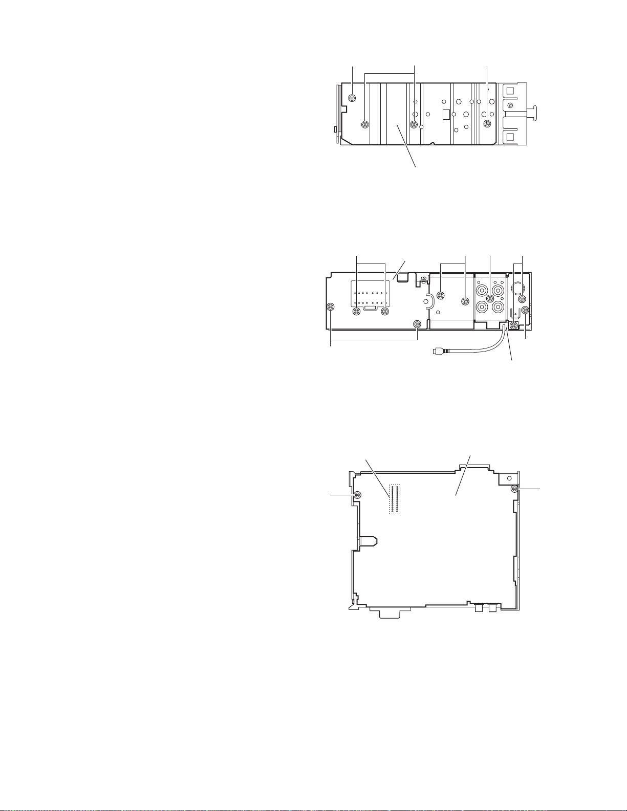
2.1.4 Removing the heat sink
(See Fig.4)
• Prior to performing the follo wing procedure, remove the front
panel assembly as required.
(1) Remove the two screws B and two screws C attaching the
heat sink on the left side of the main body, and remove the
heat sink.
2.1.5 Removing the rear bracket
(See Fig.5)
• Prior to performing the following procedure, remove the bottom
cover.
(1) Remove th e th ree screws D, screw E and six screws F at-
taching the rear bracket on the back side of the main body.
(2) Remove the rear bracket.
Reference:
During reassembly, before fixing the rear bracket onto the
main body, insert the video out cable into the slot.
C
FF
B
Heat sink
Fig.4
Rear bracket
F
C
E
2.1.6 Removing the main board
(See Fig.6)
• Prior to performing the follo wing procedure, remove the front
panel assembly, front chassis assembly, heat sink, bottom
cover and rear bracket.
(1) Remove the two screws G attaching the main board.
(2) Disconnect the connector CN501 and remove the main
board.
G
D
CN501
D
Insert the video out cable
into the slot.
Fig.5
Main board assembly
G
Fig.6
1-6 (No.49837)
Page 7
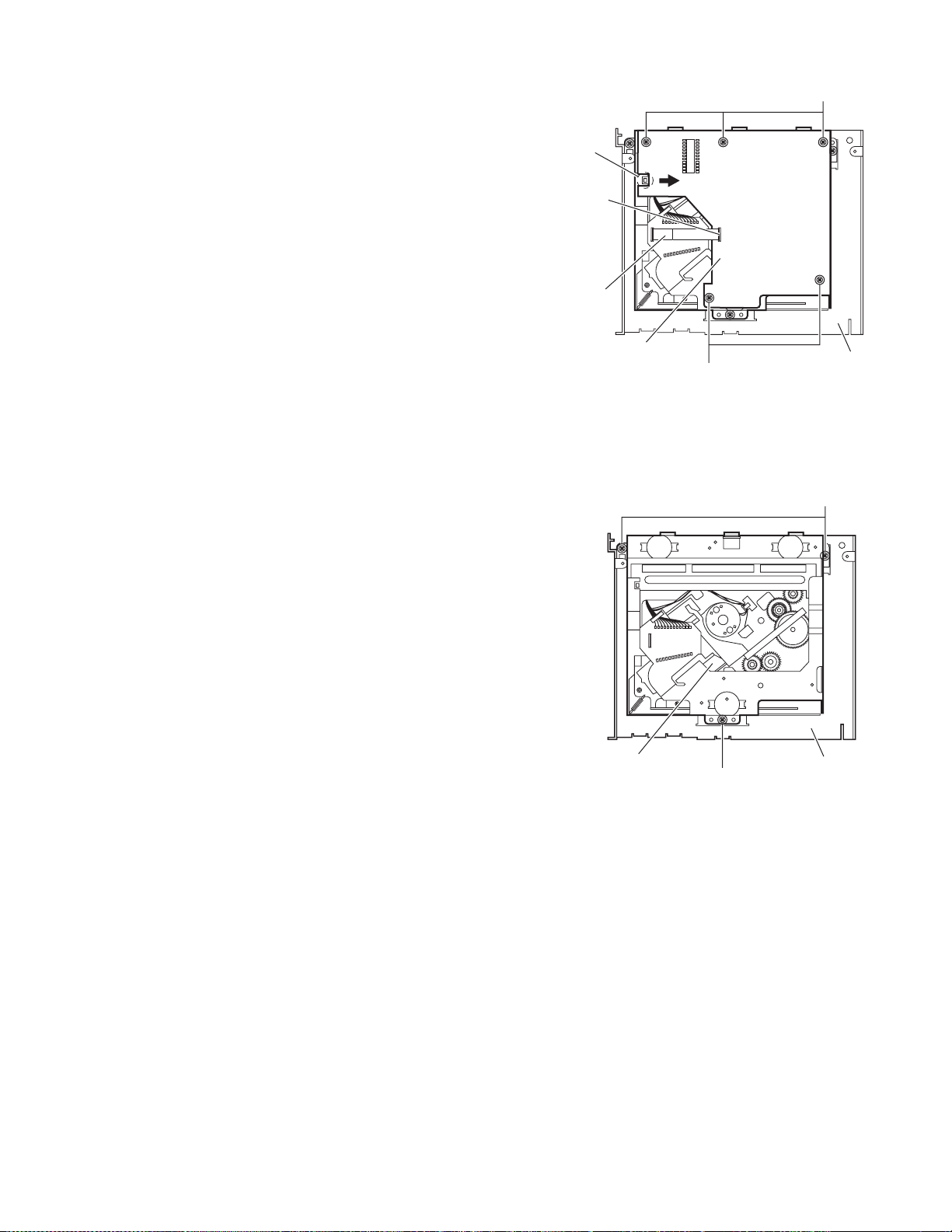
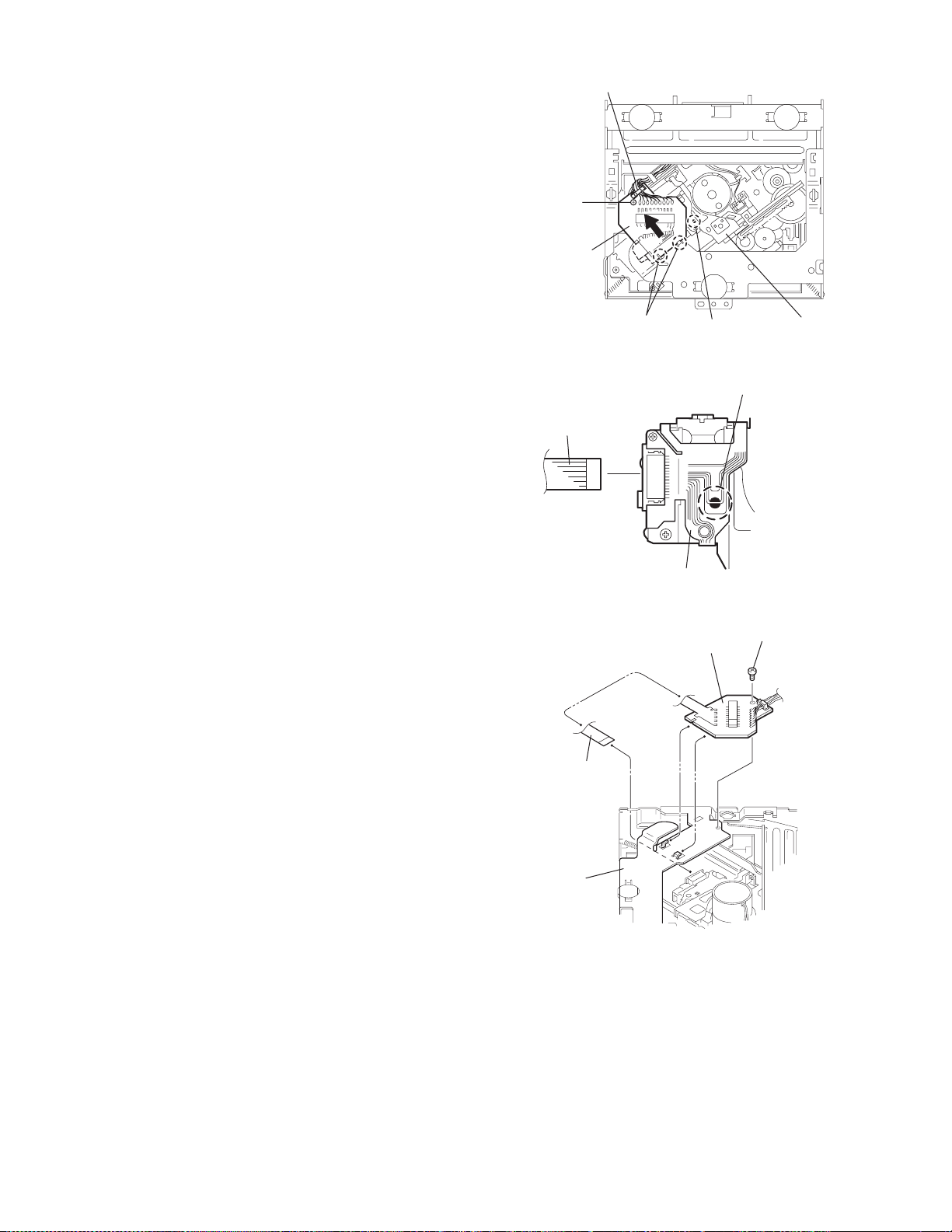
2.1.7 Removing the VCD/CD mechanism board
(See Fig. 7)
• Prior to performing the followin g procedure, remove the front
panel assembly, front chassis assembly, heat sink, bottom
cover, rear bracket and main board.
(1) Remove th e five screws H attaching the VCD/CD mecha-
nism board.
(2) Disconnect the card wire from the connector CN601 on the
VCD/CD mechanism board.
(3) Move the VCD/CD mechanism board in the direction of the
arrow to release it from the joint f.
H
Joint f
CN601
Card wire
2.1.8 Removing the CD mechanism assembly
(See Fig. 8)
• Prior to performing the followin g procedure, remove the front
panel assembly, front chassis assembly, heat sink, bottom
cover, rear bracket, main board and VCD/CD mechanism
board.
(1) Remove the three screws J attaching the top chassis.
(2) Take out the CD mechan ism as sembly.
VCD/CD mechanism board
CD mechanism assembly
Top chassis
H
Fig.7
J
Top chassis
J
Fig.8
(No.49837)1-7
Page 8
2.1.9 Removing the front board
(See Figs.9 to 11)
• Prior to performing the follo wing procedure, remove the front
panel assembly.
(1) Remove the four screws K on the back side of the front
panel assembly. (See Fig.9.)
(2) Release the thirteen joints g. (See Fig.10.)
(3) Release the joint h and take out the front board. (See
Fig.11.)
K
K
Fig.9
Joints g Joints g
Joints g
Front board
Joints g
Fig.10
Joint h
K
Joints g
Joints g
Front panel assembly
Fig.11
1-8 (No.49837)
Page 9
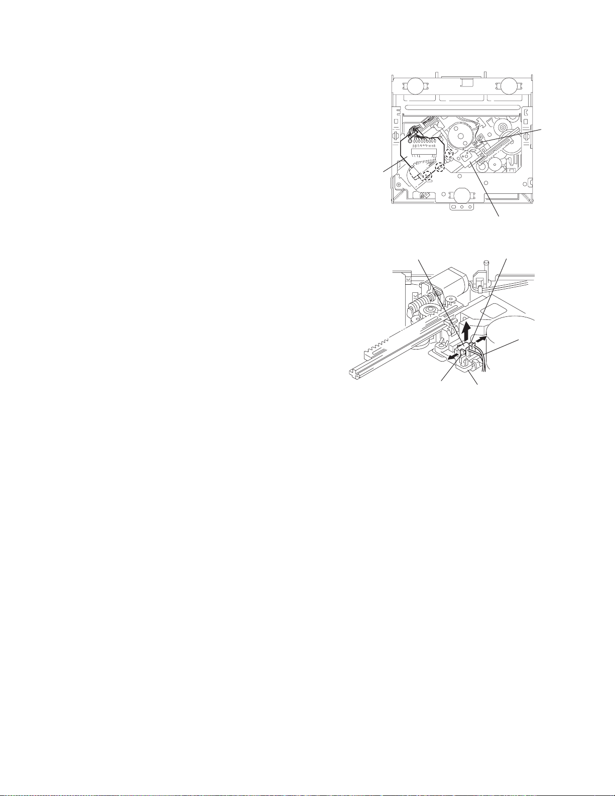
2.2 CD Mechanism section
A
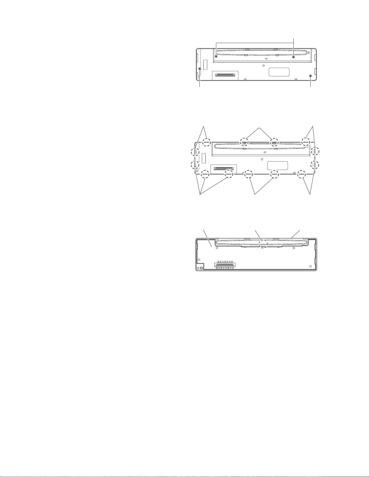
2.2.1 Removing the top cover
(See Figs.1 and 2)
(1) Remove the four screws A on the both side of the body.
(2) Lift the front side of the top cover an d move the top cover
backward to release the two joints a.
Top cover
Joints a
A
Joints a
A
Fig.1
Fig.2
Top cover
(No.49837)1-9
Page 10
2.2.2 Removing the connector board
(See Figs.3 to 5)
CAUTION:
Before disconnecting the flexible wire from the pickup, solder
the short-circuit point on the pickup. No observance of this instruction may cause damage of the pickup.
(1) Remove the screw B fixing the connector board.
(2) Solder the short-circuit point on the pickup.
(3) Disconnect the flexible wire from the pickup.
(4) Move th e connector board in the direction of the arrow to
release the two joints b.
(5) Unsolder the wires on the connector board if necessary.
CAUTION:
Unsolder the short-circuit point after reassembling.
B
Connector board
Flexible wire
Wires
Joints b
Short-circuit point
Fig.3
Short-circuit point
(Soldering)
Pickup
Flexible wire
Frame
Pickup
Fig.4
B
Connector board
Fig.5
1-10 (No.49837)
Page 11
2.2.3 Removing the DET switch
(See Figs.6 and 7)
(1) Exten d the two tabs c of the feed sw. hol der and pull out
the switch.
(2) Unsolder the DET switch wire if necessary.
DET
switch
Connector
board
Pickup
Fig.6
DET switch
Tab c
Tab c
DET switch wire
Feed sw. holder
Fig.7
(No.49837)1-11
Page 12
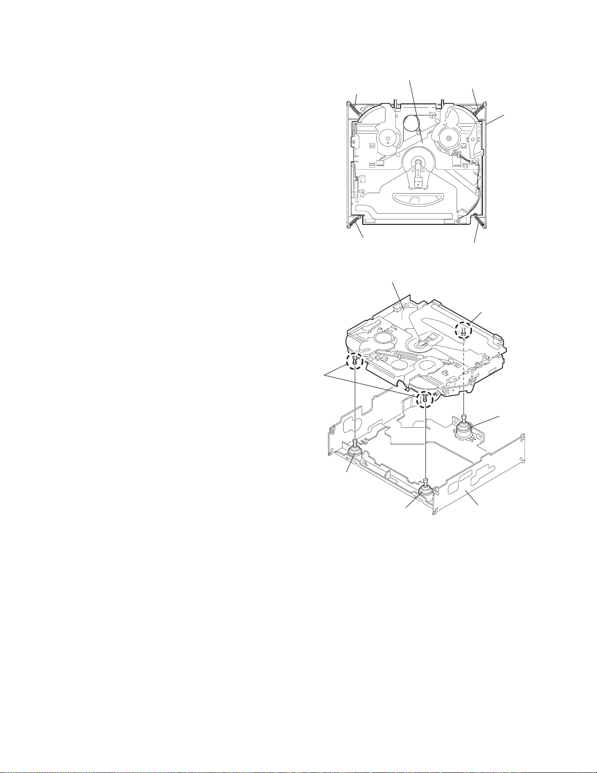
2.2.4 Removing the chassis unit
r
(See Figs.8 and 9)
• Prior to performing the following procedure, remove the top
cover and connector board.
(1) Remove the two suspension springs (L) and (R) attaching
the chassis unit to the frame.
CAUTION:
• The shape of the suspension spring (L) and (R) are different. Handle them with care.
• When reassembling, make sure that the three shafts
on the underside of the chassis unit are inserted to the
dampers certainly.
Suspension spring (R)
Chassis unit
Suspension spring (L)
Frame
Suspension spring (R)
Chassis unit
Shafts
Damper
Damper
Suspension spring (L)
Fig.8
Shaft
Dampe
Frame
Fig.9
1-12 (No.49837)
Page 13
2.2.5 Removing the clamper assembly
(See Figs.10 and 11)
• Prior to performi ng the following procedure, remove the top
cover.
(1) Remove the clamper arm spring.
(2) Move the clamper assembly in the direction of the arrow to
release the two joints d.
Clamper arm
spring
Joint d
Joint d
Clamper assembly
Fig.10
Clamper arm spring
Chassis rivet
assembly
Joint d
Clamper assembly
Chassis rivet assembly
Joint d
Fig.11
(No.49837)1-13
Page 14
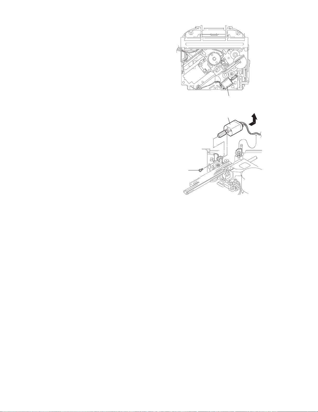
2.2.6 Removing the loading / feed motor assembly
(See Figs.12 and 13)
• Prior to performing the following procedure, remove the top
cover, connector board and chassis unit.
(1) Remove the screw C and move the loading / feed motor as-
sembly in the direction of the arrow to remove it from the
chassis rivet assembly.
(2) Disconnect the wire from the loading / feed motor assembly
if necessary.
CAUTION:
When reassembling, connect the wire from the loadin g /
feed motor assembly to the flame as shown in Fig.12.
Loading / feed motor assembly
Fig.12
Loading / feed motor assembly
C
Fig.13
1-14 (No.49837)
Page 15
2.2.7 Removing the pickup unit
r
(See Figs.14 to 18)
• Prior to performi ng the following procedure, remove the top
cover, connector board and chassis unit.
(1) Remove the screw D and pull out the pu. shaft holder from
the pu. shaft.
(2) Remove the screw E attaching the feed sw. holder.
(3) Move the part e of the pickup unit upward with the pu. shaft
and the feed sw. holder, then release the joint f of the feed
sw. holder in the direction of the arrow. The joint g of the
pickup unit and the feed rack is released, and the feed sw.
holder comes off.
(4) Remove the pu. shaft from the pickup unit.
(5) Remove the screw F attaching the feed rack to the pickup
unit.
2.2.8 Reattaching the pickup unit
(See Figs.14 to 17)
(1) Reattach the feed rack to the pickup unit using the screw F.
(2) Reattach the feed sw. holder to the feed rack while setting
the joint g to the slot of the feed rack and setting the joint f
of the feed rack to the switch of the feed sw. holder correctly.
(3) As the feed sw. holder is temporarily attached to the pickup
unit, set to the gear of the joint g and to the bending part of
the chassis (joint h) at a time.
CAUTION:
Make sure that the part i on the underside of the feed
rack is certainly inserted to the slot j of the change lock
lever.
(4) Reattach th e feed sw. holder using the screw E.
(5) Reattach th e pu. shaft to the pickup unit. Reatta ch the pu.
shaft holder to the pu. shaft using the screw D.
Part e
Joint g
Feed sw. holder
Feed rack
Part i
E
Slot j
F
Fig.15
Pu. shaft
Pickup unit
Joint f
Joint h
Fig.16
Feed rack
Pickup unit
Feed sw. holder
D
Pu. shaft holde
Joint f
Pu. shaft
D
Pu. shaft holder
Feed sw. holder
Pickup unit
Fig.14
Part e
E
Joint g
Pickup unit
Feed rack
Fig.17
Pickup unit
Joint g
Joint f
Feed sw. holder
Fig.18
(No.49837)1-15
Page 16

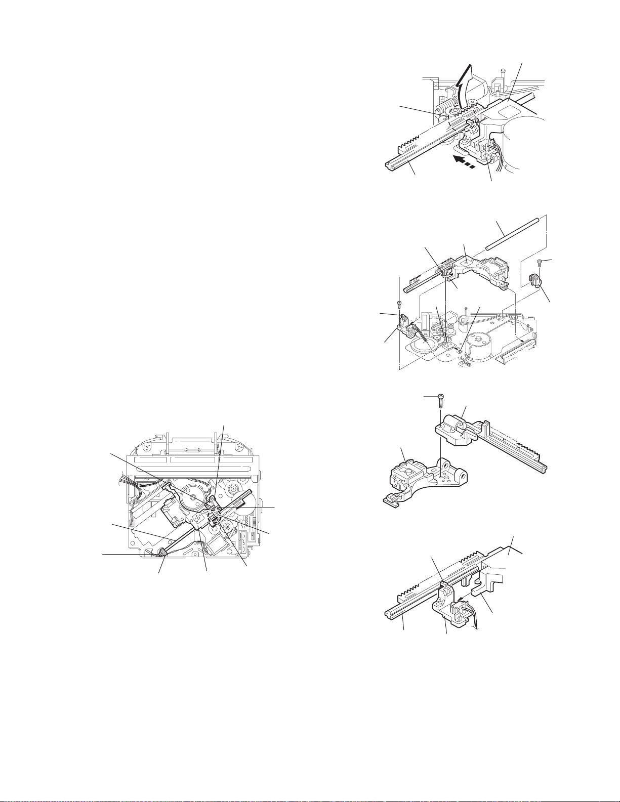
2.2.9 Removing the trigger arm
r
(See Figs.19 and 20)
• Prior to performing the following procedure, remove the top
cover, connector board and clamper unit.
(1) Turn the trigger arm in the direction of the arrow to release
the joint k and pull out upward.
CAUTION:
When reassembling, insert the part m and n of the trigger
arm into the part p and q at the slot of the chassis rivet
assembly respectively and join the joint k at a time.
Chassis rivet assembly
Trigger arm
Chassis
rivet
assembly
Joint k
Trigger arm
Fig.19
Part p
Part q
Part m
Part n
2.2.10 Removing the top plate assembly
(See Fig.21)
• Prior to performing the following procedure, remove the top
cover, connector board, chassis unit, and clamper assembly.
(1) Remove the screw H.
(2) Move the top plate assembly in the direction of the arrow to
release the two joints r.
(3) Unsolder the wire marked s if necessary.
H
Fig.20
Top plate assembly
Joints
s
Fig.21
1-16 (No.49837)
Page 17

2.2.11 Removing the mode sw. / select lock arm
(See Figs.22 and 23)
• Prior to performi ng the following procedure, remove the top
plate assembly.
(1) Bring up the mode sw. to release from the link plate (joint t)
and turn in the direction of the arrow to release the joint u.
(2) Unsolder the wire of the mode sw. marked s if necessary.
(3) Turn the select lock arm in the dire cti on of the arrow to re-
lease the two joints v.
(4) The select lock arm spring comes off the select lock arm at
the same time.
Link plate
Joint u
Fig.22
Joint t
Mode sw.
Select lock arm
s
Top plate
Select lock arm
Link plate
Select lock arm
Fig.23
Top plate
Hook w
Select lock
arm spring
Joints v
(No.49837)1-17
Page 18

2.2.12 Reassembling the mode sw. / select lock arm
(See Figs.24 to 26)
REFERENCE:
Reverse the above removing procedure.
(1) Reattach the select lock arm spring to the top plate and set
the shorter end of the select lock arm spring to the hook w
on the top plate.
(2) Set the other longer end of the select lock arm spring to the
boss x on the underside of the select lock arm, and join the
select lock arm to the slots (joint v). Turn the select lock
arm as shown in the figure.
(3) Reattach the mode sw. while setting the part t to th e first
peak of the link plate gear, and join the joint u.
CAUTION:
When reattaching the mode sw., check if the points y and
z are correctly fitted and if each part operates properly.
Select lock arm spring
Hook w
Joint v
Joint v
Select lock arm
Boss x
Fig.24
Joint t
Point y
Link plate
Point z
Link plate
Fig.25
Mode sw.
Select
lock arm
Joint t
Joint u
Fig.26
1-18 (No.49837)
Page 19

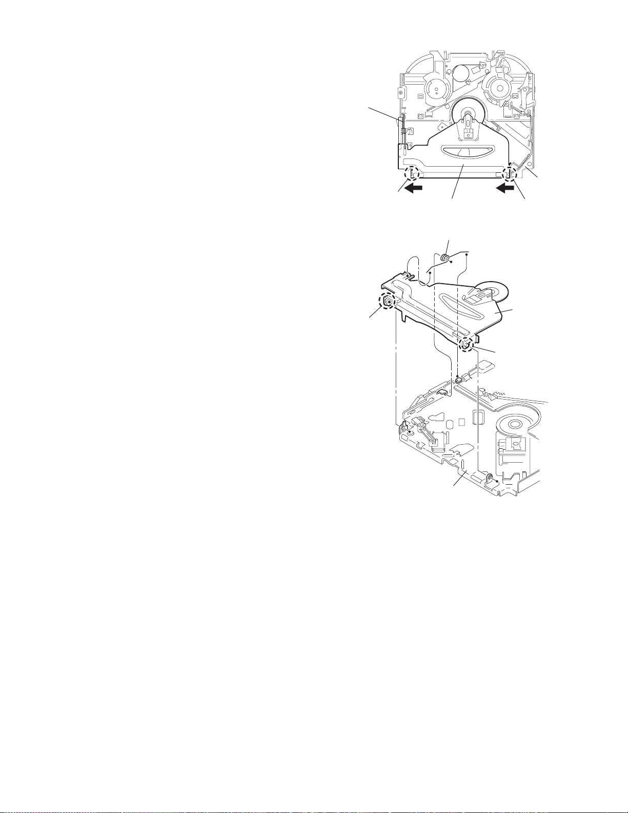
2.2.13 Removing the select arm R / link plate
(See Figs.27 and 28)
• Prior to performi ng the following procedure, remove the top
plate assembly.
(1) Bri ng up the select arm R to release from the link plate
(joint a') and turn as shown in the figure to release the two
joints b' and joint c'.
(2) Move the link plate in th e direction of the arrow to release
the joint d'. Remove the link plate spring at the same time.
REFERENCE:
Before removing the link plate, remove the mode sw..
Select arm R
Joint b'
Link plate spring
Joint c'
Joint a'
Link plate
Joint b'
Fig.27
Joint r
2.2.14 Reattaching the Select arm R / link plate
(See Figs.29 and 30)
REFERENCE:
Reverse the above removing procedure.
(1) Reattach th e link plate spring.
(2) Reattach the li nk plate to the link pla te spri ng while j oini ng
them at joint d'.
(3) Reattach the joint a' of the select arm R to the first peak of
the link plate while joining the two joints b' with the slots.
Then turn the select arm R as shown in the figure. The top
plate is joined to the joint c'.
CAUTION:
When reattaching the sele ct arm R, check if the points e'
and f' are correctly fitted and if each part operates properly.
Top plate
Select arm R
Joint b'
Joint d'
Link plate
Fig.28
Link plate spring
Joint c'
Joint d'
Joint b'
Joint a'
Fig.29
Joint a'
Point e'
Link plate
Point f'
Fig.30
(No.49837)1-19
Page 20

2.2.15 Removing the loading roller assembly
(See Figs.31 to 33)
• Prior to performing the following procedure, remove the
clamper assembly and top plate assembly.
(1) Push inw ard the loading roller assembly on the gear side
and detach it upward from the slot of the joint g' of the lock
arm rivet assembly.
(2) Detach the loading roller assembly from the slot of the joint
h' of the lock arm rivet assembly.
The roller guide comes off the gear section of the loading
roller assembly.
Remove the roller guide and the HL washer from the shaft
of the loading roller assembly.
(3) Remove the screw J attaching the lock arm rivet assembly.
(4) Push th e shaft at the joint i' of the lock arm rivet assembly
inward to release the lock arm rivet assembly from the slot
of the L side plate.
(5) Extend the lock arm rivet assembl y outward and release
the joint j' from the boss of the chassis rivet assembly. The
roller guide springs on both sides come off at the same
time.
CAUTION:
When reassembling, reattach the left and right roller
guide springs to the lock arm rivet assembly before reattaching the lock arm rivet assembly to the chassis rivet
assembly. Make sure to fit the part k' of the roller guide
spring inside of the roller guide. (Refer to Fig.34.)
Roller guide
spring
Part k'
Chassis rivet assembly
Loading roller assembly
Loading roller assembly
Roller guide
spring
Fig.32
Boss
Roller guide
Joint h'
Roller guide spring
Loading roller assembly
HL washer
Loading roller assembly
Joint g'
Lock arm rivet assembly
Fig.31
Roller guide
Roller guide spring
Roller guide spring
J
Lock arm rivet assembly
Lock arm rivet assembly
L side plate
Roller guide spring
Joint i'
Joint j'
Fig.33
Roller guide
HL washer
Roller shaft assembly
Loading roller
Roller guide spring
Fig.34
1-20 (No.49837)
Page 21

2.2.16 Removing the loading gear 5, 6 and 7
(See Figs.35 and 36)
• Prior to performi ng the following procedure, remove the top
cover, chassis unit, pickup unit and top plate assembly.
(1) Remove the screw K atta ching the loading gear bracket.
The loading gear 6 and 7 come off the loading gear bracket.
(2) Pull out the loading gear 5.
K
Loading gear 5
Loading gear bracket
K
Loading gear 6
Loading gear 5
Loading gear 3
Fig.35
Loading gear bracket
Loading gear 6
Loading gear 7
Fig.36
(No.49837)1-21
Page 22

2.2.17 Removing the gears
(See Figs.37 to 40)
• Prior to performing the following procedure, remove the top
cover, chassis unit, top plate assembly and pickup unit.
• Pull out the loading gear 3. (See Fig.35.)
(1) Pull out the feed gear.
(2) Move the load ing pl ate assembly i n the dire ctio n of the ar-
row to release the L side plate from the two slots m' of the
chassis rivet assembly. (See Fig.37.)
(3) Detach the loading pla te assembly upward from the chas-
sis rivet assembly while releasing the joint n'. Remove the
slide hook and loading plate spring from the loading plate
assembly.
(4) Pull out the loading gear 2 and remove the change lock le-
ver.
(5) Remov e the E ring and wa sher atta ching th e change gear
2.
(6) The change gear 2, change gear spring and adjusting
washer come off.
(7) Remov e the loading gear 1.
(8) Move the change plate rivet assembly in the direction of the
arrow to release from the three shafts of the chassis rivet
assembly upward. (See Fig.38.)
(9) Detach the loading gear plate rivet assembly from the shaft
of the chassis rivet assembly upward while releasing the
joint p'. (See Figs.38 and 40.)
(10) Pull out the loading gear 4.
Change plate
rivet assembly
Shafts
E ring
Loading plate assembly
Loading plate spring
Joint p'
Loading gear 4
Loading gear plate
rivet assembly
Shaft
Loading gear 2
Loading gear 1
Chassis rivet assembly
Change gear 2
Fig.38
Joint n'
Slide hook
Feed gear
Fig.37
Slot m'
L side plate
Loading plate assembly
Joint n'
Slot m'
Chassis rivet assembly
Chassis rivet assembly
E ring
Washer
Change gear 2
Change gear
spring
Adjusting
washer
Change plate
rivet assembly
L side plate
Slot m'
Slot m'
Fig.39
Loading gear 1
Loading gear 2
Change lock lever
Loading gear 4
1-22 (No.49837)
Chassis rivet assembly
Loading gear plate rivet
assembly
Fig.40
Page 23

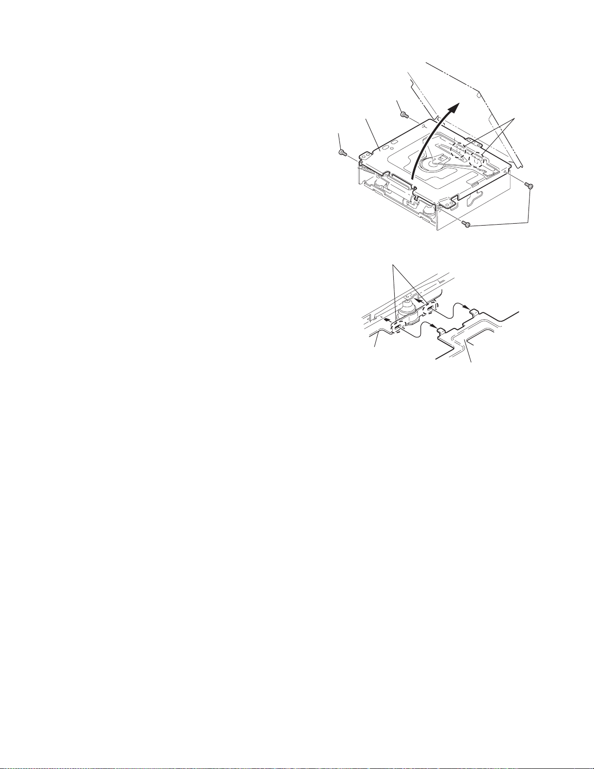
2.2.18 Removing the turn table / spindle motor
(See Figs.41 and 42)
• Prior to performi ng the following procedure, remove the top
cover, connector board, chassis unit and clamper assembly.
(1) Remove the two screws L a ttaching the spindle motor as-
sembly through the slot of the turn table on top of the body.
(2) Unsolder the wire on the connector board if necessary.
Turn table
L
Fig.41
L
Turn table
Spindle motor
Fig.42
(No.49837)1-23
Page 24

SECTION 3
Adjustment
3.1 Adjustment method Test instruments required for adjustment
(1) Digital oscilloscope (100MHz)
(2) AM Standard sign al generator
(3) FM Standard signal generator
(4) Stereo modulator
(5) Electric voltmeter
(6) Digital tester
(7) Tracking offset meter
(8) Test Disc JVC :CTS-100 0
(9) Extension ca ble for check
EXTSH002-22P × 1
Standard volume position
Balance and Bass &Treble volume : lndication"0"
Loudness : OFF
How to connect the extension cable for adjusting
Caution:
Be sure to attach the heat sink and rear bracket onto the power amplifier IC and regulator IC respectively, before supply the power.
If voltage is applied without attaching these parts, the power amplifier IC and regulator IC will be destroyed by heat.
Standard measuring conditions
Power supply voltage DC14.4V(11 to 16V)
Load impedance 20KΩ(2 Speakers connection)
Output Level Line out 2.0V (Vol. MAX)
Dummy load
Exclusive dummy load should be used for AM,and FM. For FM
dummy load,there is a loss of 6dB between SSG output and
antenna input.The loss of 6dB need not be considered since
direct reading of figures are applied in this working standard.
1-24 (No.49837)
Extension cable
EXTSH002-22P
Heat sink
(Attach the heat sink
using the two screws.)
Rear bracket
(Attach the rear bracket
using the screw.)
CN501
Page 25

3.2 Service mode
Operation method
Insert the test disc
"TOC read" starts
Press the [CD], [SEL]
and [POWER] keys
simultaneously for 2 seconds.
"VERSION" is
indicated on the LCD.
Press the [SEL] key
"MAIN 400" is
indicated on the LCD.
Press the [F.SKIP] key
"SUB 225" is
indicated on the LCD.
MAIN 400
SUB 225
(Note)
If "SUB 000" and "VCD 000"
are indicated on the LCD,
these operations are required.
Main micon software version
Space
Sub micon software version
Press the [F.SKIP] key
"SUB 144" is
indicated on the LCD.
Press the [F.SKIP] key
Sequence of LCD diaplay
Press the [F.SKIP] . . . . . . . . MAIN SUB VCD/CD MAIN
Press the [B.SKIP] . . . . . . . . MAIN VCD/CD SUB MAIN
Cancellation of service mode
No operation for ten seconds Return to normal display
Press the key except for [F.SKIP] or [B.SKIP] key Return to normal display
VCD 144
VCD/CD control IC software version
(No.49837)1-25
Page 26

3.3 Maintenance of laser pickup
(1) Cleani ng the pick up lens
Before you replace the pick up, please try to clean the lens
with a alcohol soaked cotton swab.
(2) Life of the laser diode
When the life of the laser diode has expired, the following
symptoms will appear.
• The level of RF output (EFM output: amplitude of eye
pattern) will be low.
3.4 Replacement of laser pickup
Turn off the power switch and,disconnect the
power cord from the ac outlet.
Replace the pickup with a normal one.(Refer
to "Pickup Removal" on the previous page)
Is RF output
1.3 0.4Vp-p?
NO
Replace it.
YES
O.K
(3) Semi-fixed resistor on the APC PC board
The semi-fixed resistor on the APC printed circuit board
which is attached to the pickup is used to adjust the laser
power.Since this adjustment should be performed to match
the characteristics of the whole optical block, do not touch
the semi-fixed resistor.
If the laser power is lower than the specified value, the laser diode is almost worn out, and the laser pickup should
be replaced. If the semi-fixed resistor is adjusted while the
pickup is functioning normally, the laser pickup may be
damaged due to excessive current.
Plug the power cord in,and turn the power on.
At this time,check that the laser emits for
about 3seconds and the objective lens moves
up and down.
Note: Do not observe the laser beam directly.
Play a disc.
Check the eye-pattern at RF test point.
Finish.
1-26 (No.49837)
Page 27

SECTION 4
A
A
A
A
A
A
A
A
O
4
3
1
0
P
A
Description of major ICs
4.1 AT27C020-70JCU5 (IC102) : 2M-bit (256K x 8) OTP EPROM
• Pin Layout
• Block Diagram
A12
432
5
7
6
6
7
5
8
4
9
3
10
2
11
1
12
0
13
0
14151617181920
O1
VCCPGMA17
A15
A16
VP
1
323130
O3O4O5
O2
ND
VCC
GND
VPP
CE
PGM
A0 - A17
DDRESS
INPUTS
OE
29
28
27
26
25
24
23
22
21
O6
A1
A1
A8
A9
A1
OE
A1
CE
O7
OE,CE AND
PROGRAM LOGIC
Y DECODER
X DECODER
DATA OUTPUTS
O0 - O7
OUTPUT
BUFFERS
Y-GATING
CELL MATRIX
IDENTIFICATION
• Pin function
Pin No. Symbol Function
1 VPP Power supply
2 A16 Address input
3 A15 Address input
4 A12 Address input
5 to 12 A7 to A0 Address inputs
13 to 15 O0 to O2 Outputs
16 O3 to O7 Outputs
17 to 21 GND Ground
22 CE Chip enable
23 A10 Address input
24 OE Output enable
25 A11 Address input
26 A9 Address input
27 A8 Address input
28 A13 Address input
29 A14 Address input
30 A17 Address input
31 PGM Program strobe
32 VCC Power supply
(No.49837)1-27
Page 28

4.2 ES3880FM (IC101) : Video CD processor
• Pin Layout
75 ~ 51
76
50
• Block Diagram
100
~
1 ~ 25
Serial Audio
TDM
Interface
Interface
~
26
Transport
Parser
32-Bit
RISC Processor
8KB cache
On-Screan
Display
Gateway and
DMA Controller
CRT
Controller
Huffman
Decoder
DRAM
Interface
Video
Processor
• Pin function
Pin No. Symbol I/O Descriptions
1 VDD I 2.85V power supply.
2 RAS# O Memory row address strobe (active-low).
3 DWE# O Memory write enable (active-low).
4~12 MA[8:0] O Multiplexed memory row and column address.
13~28 DBUS[0:15] I/O Memory data.
29 RESET# I System reset (active-low)
30 VSS I Ground.
31 VDD I 2.85V power supply.
32~39 YUV[0:7] O B-bit YUV output.
40 VSYNC I/O Vertical sync; programmable for rising or falling edge.
41 HSYNC I/O Horizontal sync; programmable for rising or falling edge.
42 CPUCLK I RISC and system clock input.
43 PCLK2X I/O Doubled pixel clock I/O for screen video interface.
44 PCLK I/O 27-MHz pixel clock qualifier I/O for screen video interface.
45~49 AUX[0:7] I/O Auxillary control (AUX0 and AUX1 are open collectors).
50 VSS I Ground.
51 VDD I 2.85V power supply.
52~54 AUX[0:7] I/O Auxillary control (AUX0 and AUX1 are open collectors).
55~62 LD[0:7] I/O RISC interface data.
1-28 (No.49837)
Page 29

Pin No. Symbol I/O Descriptions
63 LWR# O RISC interface write enable (active-low).
64 LOE# O RISC interface output enable (active-low).
65~67 LCS[3,1,0]# O RISC interface chip select (active-low).
68~79 LA[0:17] O RISC interface address.
80 VSS I Ground.
81 VPP I 5.0V power supply.
82~87 LA[0:17] O RISC interface address.
88 ACLK I/O Master clock for external audio DAC (8.192MHz, 11.2896MHz,
12.288MHz, 16.9344MHz, and 18.432MHz).
89 AOUT O Audio interface serial data.
SEL_PLL0 I Used with SEL_PLL1 pin 91 to select phase-lock loop (PLL) clock
frequency of CPUCLK pin 42:
00 = bypass PLL.
01 = 54MHz PLL.
10 = 67.5MHz PLL.
11 = 81MHz PLL.
90 ATCLK I/O Audio transmit bit clock.
91 ATFS O Audio interface transmit frame sync.
SEL_PLL1 I Used with SEL_PLL0 pin 89 to select phase-lock loop (PLL) clock
frequency of CPUCLK pin 42,
92 MA9 O Multiplexed memory row and column address.
DOE# O Memory output enable (active-low).
93 AIN I Audio interface serial data.
94 ARFS I Audio receive bit clock.
95 ARCLK I Audio interface receive frame sync.
96 TDMCLK I TDM serial clock.
97 TDMDR I TDM serial data receive.
98 TDMFS I TDM frame sync.
99 CAS# O Memory colomn address strobe (active-low).
100 VSS I Ground.
4.3 TC7 W08FU-X (IC107) : Nand gate
• Pin layout & Block diagram • Truth table
1A
1
8
Vcc
ABY
LLL
1B
2Y
GND
2
3
4
7
1Y
6
2B
5
2A
LHL
HLL
HHH
(No.49837)1-29
Page 30

4.4 ES3883F(IC104):VCD Companion chip
• Pin function
80
81
~
~
51
50
~
100
31
1
• Blockdiagram
30~
CD-ROM Controller
CD ROM
Kit
Remote
Control
Interrupt
Control
Audio DAC
Vista ES3880
(Video CD)
DSC
NTSC/PAL Video
PLL
ROM
Mic 1
DRAM
• Pin function
Pin No. Symbol I/O Function
1,25:26,31,72,75,77,91,100 VSS I Ground.
5,16,32,66,73,78,90 VCC I Voltage supply 5v.
6 DSC_C I Clock programming to access internal registers.
7 AUX0 I/O Servo Foward or Control Pin.
9 AUX1 I/O Servo Reverse or Control Pin.
11 AUX2 I/O Servo LDON or Control Pin.
70 AUX3 I/O Servo CW/Limit or Control Pin.
69 AUX4 I/O Servo CCW/Close or Control Pin.
68 AUX5 I/O Servo Data or Control Pin.
67 AUX6 I/O Servo XLAT or Control Pin/VFD_DO.
14 AUX7 I/O Servo BRKM/Sense or Control Pin/VFD_DI.
18 AUX8 I/O Servo Mute/Open or Control Pin/VFD_CLK.
20 AUX9 I/O Servo SQS0 or Control Pin.
34 AUX10 I/O Servo SQCK or Control Pin.
35 AUX11 I/O 3880 IRQ or Interrupt Output or Control Pin.
36 AUX12 I/O CD C2PO or Interrupt input or Control Pin.
38 AUX13 I/O Serial Interrupt/CD-Mute or Control Pin.
39 AUX14 I/O Servo SCOR(S0S1) or Interrupt Input or Control Pin.
40 AUX15 I/O Interrupt Input or Control Pin.
81,83,85,93,95,97,99,8 DSC_D[7:0] I/O Data for programming to access Internal registers.
10 DSC_S I Strobe for programming to access Internal registers.
12 DCLK O Dual-purpose pin DCLK is the MPEG decoder clock.
EXT_CLK I EXT_CLK is the external clock EXT_CLK is an input during bypass PLL mode.
13 RESET_B I Video reset(active-low).
15 MUTE O Audio mute.
17 MCLK I Audio master clock.
19 TWS I Dual-purpose pin TWS is the transmit audio frame sync.
SPLL_OUT O SPL L_OUT is the select PLL output.
21 TSD I Transmit audio data input.
22 TBCK I Transmit aud io bit clock.
Mic 2
Echo/Surround/Vocal Assist
Preamp
Volume Control
Preamp
Volume Control
VFD
Driver
Remote
receiver
Speakers
Television
VFD
Panel
1-30 (No.49837)
Page 31

Pin No. Symbol I/O Function
23 RWS O Dual-purpose pin RWS is the audio frame sync.
SEL_PLL1 I Pins SEL_PLL[1.0] select the PLL clock frequency for the DCLK output.
SEL_PLL1 SEL_PLL0 DCLK
0 0 Bypass PLL(input mode)
0 0 27 MHz(output mode)
1 0 32.4 MHz(output mode)
1 1 40.5 MHz(output mode)
24 RSTOUT_B O Reset output(active-low).
2:4,27:30,76 NC No connect.Do not connect to these pins.
33 RSD O Dual-purpose pin. RSD is the receive audio data input.
SEL_PLL0 I SEL_PLL0 along with SEL_PLL1 select the PLL clock frequency for the
DCLK output.See the table for pin number 23.
37 RBCK O Dual-purpose pin.RBCK is the receive audio bit clock.
SER_IN I SER_IN is the serial input DSC mode.
0-Parallel DSC mode.
1-Serial DSC mode.
41,51 VSSAA I Audio Analog Ground.
42 VCM I ADC Common Mode Reference(CMR) buffer output.CMR is approximately
2.25V.Bypass to analog ground with 47µF electrolytic in parallel with 0.1µF.
43 VREFP I DAC and ADC maximum reference.
Bypass to VCMR with 10µF in parallel with 0.1µF.
44 VCCAA I Analog VCC, 5V.
45:46 AOR+,AOR- O Right channel output.
47:48 AOL-,AOL+ O Left channel input.
49 MIC1 I Microph one input 1.
50 MIC2 I Microphone 2.
52 VREF I Internal resistor divider generates Common Mode Reference(CMR) voltage.
Bypass to analog ground with 0.1µF.
53 VREFM I DAC and ADC minimum reference.
Bypass to VCMR with 10µF in parallel with 0.1µF.
54 RSET I Full scale DAC current adjustment.
55 COMP I Compensation pin.
56:57,62:63 VSSAV I Video Analog Ground
58 CDAC O Modulates chrominance output.
59,60 VCCAV I Video VCC, 5V
61 YDAC O Y Iuminance data bus for screen video port.
64 VDAC O Composite video output.
65 ACAP I Audio CAP.
71 XOUT O Crystal output.
74 XIN I 27 MHz crystal input.
79 PCLK I/O 13.5 MHz pixel clock.
80 2XPCLK I/O 27 MHz(2 times pixel clock).
82 HSYN_B O Horizontal sync(active-low).
84 VSYN_B O Vertical sunc(active-low).
86:89,92,94,96,98 YUV[7:0] I YUV data bus for screen video port.
(No.49837)1-31
Page 32

4.5 AN22000A (IC601) : RF & SERVO AMP
• Terminal layout
ACBDPDF
323130292827262524232221201918
123456789
LD
PD
VCC
RFN
PDE
RFIN
RFOUT
TBAL
FBAL
GCTRL
FEOUT
10111213141516
ARF
CEA
CAGC
3TOUT
FEN
TEN
BDO
CBDO
TEOUT
TEBPF
OFTR
COFTR
• Block diagram
32
31
30
29
27
28
RFOUT
RF_EQ
AMP
AMP
AMP
AMP17GCA BCA
+
-
624754 8
RFIN
AGC
NRFDET
GCA BCA
GCA BCA
GCA BCA
11 12
BDO
SUBT
SUBT
VDET
VREF
17
GND
RFDET
13 14
OFTR
3TENV
VDET
• Pin function
Pin
Symbol I/O Function
No.
1 PD I APC Amp. input terminal
2 LD O APC Amp. output terminal
3 VCC - Power supply terminal
4 RFN I RF adder Amp. inverting input terminal
5 RFOUT O RF adder Amp. output terminal
6 RFIN I AGC input terminal
7 CAGC I Input terminal for AGC loop filter capacitor
8 ARF O AGC output terminal
9 CEA I Capacitor connecting terminal
for HPF-Amp.
10 3TOUT O 3 TENV output terminal
9
11 CBDO I Capacitor connecting terminal for envelope
detection on the darkness side
10
12 BDO O BDO output terminal
13 COFTR I Capacitor connecting terminal for envelope
15
detection on the light side
14 OFTR O OFTR output terminal
22
-
+
23
15 NRFDET O NRFDET output terminal
16 GND - Ground
17 VREF O VREF output terminal
18 VDET O VDET output terminal
21
-
+
20
19 TEBPF I VDET output terminal
20 TEOUT O TE Amp. output terminal
21 TEN I TE Amp. inverting input terminal
22 FEN I FE Amp. inverting input terminal
23 FEOUT O FE Amp. output terminal
19
18
24 GCTL O GCTL & APC terminal
25 FBAL O FBAL control terminal
26 TBAL O TBAL control terminal
27 E I Tracking signal input terminal 1
28 F I Tracking signal input terminal 2
29 D I Focus signal input terminal 4
-
+
2
LD
30 B I Focus signal input terminal 3
31 C I Focus signal input terminal 2
32 A I Focus signal input terminal 1
1-32 (No.49837)
GCTL26TBAL
25 16 3
FBAL
PD
1
Page 33

4.6 GLT44016-35J4-X (IC103) : Dram
A
A
A
A
A
•Pin layout •Pin function
A
A1
A2
A3
1
1
2
3
4
5
4
6
7
5
8
6
9
7
10
8
11
12
13
14
15
16
0
17
18
19
20
40
39
38
37
36
35
34
33
32
31
30
29
28
27
26
25
24
23
22
21
Vss
16
DQ
DQ
15
14
DQ
DQ
13
Vss
12
DQ
DQ
11
DQ
10
DQ9
NC
LCAS
UCAS
OE
A
8
7
A
A
6
5
A
A
4
Vss
Pin Name Functi on
A
0~A8
RAS
UCAS
LCAS
WE
OE
~DQ16Dara inputs / outputs
DQ
1
Vcc +5V power supply
Vss Ground
NC No connection
Vcc
DQ
DQ2
DQ3
DQ
Vcc
DQ
DQ
DQ
DQ
NC
NC
WE
RAS
NC
Vcc
• Block diagram
OE
WE
UCAS
LCAS
RAS
RAS
CLOCK
GENERATOR
CAS
CLOCK
GENERATOR
WE
CLOCK
GENERATOR
Address inpits
Row address strobe
Columu address strobe / upperbyte control
Columu address strobe / lower byte control
Write enable
Output enable
OE
CLOCK
GENERATOR
Vcc
Vss
Data I/O BUS
COLUMN DECODERS
REFRESH
COUNTER
Y
9
0
1
7
8
ADDRESS BUFFWRS
AND PREDECODERS
X0 - X
8
SeNSE AMPLIFIERS
- Y
0
8
512 16
512 16
ROW
DECODERS
MEMORY
ARRAY
512
4.7 TC7S08F-W (IC106) : Buffer
• Pin layout • Block diagram
IN B
IN A
1
2
5 4VDD
I/O
BUFFER
Vcc
I/O1
I/O2
I/O3
I/O4
I/O5
I/O6
I/O7
I/O8
I/O9
I/O10
I/O11
I/O12
I/O13
I/O14
I/O15
I/O16
Y
3
Vss
OUT X
B
GND
(No.49837)1-33
Page 34

4.8 LA47505 (IC321) : Power amp.
• Terminal layout
206
11
1
12
4
10
Stand by
Switch
Ripple
Filter
Protective
circuit
Mute
circuit
9
7
8
5
3
2
22
15
25
13
14
16
Muting &
On Time Control
Circuit
protective
circuit
17
19
18
21
23
24
1-34 (No.49837)
Page 35

• Terminal layout
AC CONT1
GND1
OUTFR-
STBY
OUTFR+
Vcc1/2
OUTRR-
GND2
OUTRR+
VREF
INRR
INFR
SGND
INFL
INRL
ONTIME
OUTRL+
GND3
OUTRL-
Vcc3/4
OUTFL+
MUTE
OUTFL-
GND4
NC
• Pin function
Pin No. Symbol Function
1 AC CONT1 Header of IC
2 GND1 Power GND
3 OUTFR- Outpur(-) for front Rch
4 STBY Stand by input
5 OUTFR+ Output (+) for front Rch
6 Vcc1/2 Power input
7 OUTRR- Output (-) for rear Rch
8 GND2 Power GND
9 OUTRR+ Output (+) for rear Rch
10 VREF Ripple filter
11 INRR Rear Rch input
12 INFR Front Rch input
13 SGND Signal GND
14 INFL Front Lch input
15 INRL Rear Lch input
16 ONTIME Power on time control
17 OUTRL+ Output (+) for rear Lch
18 GND3 Power GND
19 OUTRL- Output (-) for rear Lch
20 Vcc3/4 Power input
21 OUTFL+ Output (+) for front
22 MUTE Muting control input
23 OUTFL- Output (-) for front
24 GND4 Power GND
25 NC No connection
4.9 NJM4565V-X (IC151) : Dual ope amp
• Terminal layout & Pin function
1
2
3
4
1
8
A
+
-
7
B
+
-
6
AOUTPUT
2
A-INPUT
3
A+INPUT
4
V
5
B+INPUT
6
B-INPUT
7
B OUTPUT
8
V
5
(No.49837)1-35
Page 36

4.10 LA6589H-X (IC501) : BTL driver
• Pin layout & Block diagram
VIN1-A
1
+
VIN1+A
VCCP1
2
3
VIN1_SW
H : OP-AMP_A
L : OP-AMP_B
H
28
VIN1
L
27
VIN1-B
+
26
VIN1+B
VO1+
VO1-
VO2+
VO2-
FR
VO3+
VO3-
VO4+
4
5
6
7
Power system
FR
8
9
10
GND
Level shift Level shift
+
Level shift Level shift
33k
11k
+
It is ON/OFF as for all outputs.
5VREG(PNPTr External)
Signal system
GND
H : ON
L : OFF
Signal system
power supply
MUTE
Power system GND
+
25
24
23
22
FR
21
20
19
S-GND
VIN1-SW
MUTE
VREF_IN
FR
VCC_S
REG-OUT
REG_IN
VCCP2
VIN4G
1-36 (No.49837)
VO4-
VIN4
11
12
13
14
11k
+
33k
33k
33k
18
VIN2G
11k
+
11k
+
17
16
15
VIN2
VIN3G
VIN3
Page 37

• Pin function
S
O
V
D
G
T
I
Pin No. Symbol Function
1 VIN1-A CH1 input AMP_A reversing input
2 VIN1+A CH1 input AMP_A non-reversing input
3 VCCP1 CH1 and CH2 power steps power supply
4 VO1+ CH1 Output terminal (+)
5 VO1- CH1 Output terminal (-)
6 VO2+ CH2 Output terminal (+)
7 VO2- CH2 Output terminal (-)
8 VO3+ CH3 Output terminal (+)
9 VO3- CH3 Output terminal (-)
10 VO4+ CH4 Output terminal (+)
11 VO4- CH4 Output terminal (-)
12 VCCP2 CH3 and CH4 power steps power supply
13 VIN4 CH4 Input terminal
14 VIN4G CH4 Input terminal(For gain adjustment)
15 VIN3 CH3 Input terminal
16 VIN3G CH3 Input terminal(For gain adjustment)
17 VIN2 CH2 Input terminal
18 VIN2G CH2 Input terminal(For gain adjustment)
19 REGIN External PNP transistor base connection
20 REG-OUT 5VREG output terminal and external PNP transistor collector connection
21 VCCS Signal system power supply
22 VREFIN Standard voltage impression terminal
23 MUTE Output ON/OFF terminal
24 VIN1_SW CH1 input OP_AMP switch terminal
25 S_GND Signal system GND
26 VIN1+B CH1 AMP_B non-reversing input terminal
27 VIN1-B CH1 AMP_B reversing input terminal
28 VIN1 CH1 input terminal and input OP_AMP output terminal
*1 Frame (FR) at the center becomes system GND(P-GND) power . Please give (*O) as the lowest potential with system GND(S-
GND) signal.
*2 Be short-circuited of VCC_S (signal system power supply) and VCCP1 and VCCP2 (output steps power supply) o n the out-
side.
4.11 MN1510XN-X (IC550) : Driver
• Pin Layout • Block Diagram
VCC PS
AG
1
PS
6
3
6
Clamp
SA
2
UT
CC
3
5
GN
N
42
4
IN
bias
DRV.
6dB
5
GND
1
OU
(No.49837)1-37
Page 38

4.12 HA13164A (IC901) : Regulator
• Terminal layout
123456789101112131415
• Block diagram
ANT OUT
EXT OUT
ANT CTRL
CTRL
CD OUT
AUDIO OUT
C3
0.1u
C4
0.1u
C5
0.1u
C6
10u
2
1
7
11
12
10
VCC ACC
8
Surge Protector
BIAS TSD
15
3
TAB
C1
100u
C2
0.1u
13
ILM AJGND GND
+B
BATT.DET OUT
9
COMPOUT
6
VDD OUT
4
SW5VOUT
5
14
ACC
ILMOUT
R1
C7
0.1u
C8
0.1u
UNIT R:
C:F
note1) TAB (header of IC)
connected to GND
• Pin function
Pin No. Symbol Function
1 EXTOUT Output voltage is VCC-1 V when M or H level applied to CTRL pin.
2 ANTOUT Output voltage is VCC-1 V when M or H level to CTRL pin and H level to ANT-CTRL.
3 ACCIN Connected to ACC.
4 VDDOUT Regular 5.7V.
5 SW5VOUT Output voltage is 5V when M or H level applied to CTRL pin.
6 COMPOUT Output for ACC detector.
7 ANT CTRL L:ANT output OFF H:ANT output ON
8 VCC Connected to VCC.
9 BATT DET Low battery detect.
10 AUDIO OUT Output voltage is 9V when M or H level applied to CTRL pin.
11 CTRL L:BIAS OFF M:BIAS ON H:CD ON
12 CD OUT Output voltage is 8V when H level applied to CTRL pin.
13 ILM AJ Adjustment pin for ILM output voltage.
14 ILM OUT Output voltage is 10V when M or H level applied to CTRL pin.
15 GND Connected to GND.
1-38 (No.49837)
Page 39

4.13 MN101C30ACK1 (IC251) : Unit micon
8
3
T
• Pin Layout
64 49
1
4
16
3
17 32
• Pin function
Pin No. Symbol I/O Function
1,2 /SW1, /SW2 I SW1,SW2 input
3 /SW3 I Conne ct to ground
4 PCHKCD I Connect to ground
5 PCHKVCD I Connect to groun d
6 VREF+ I Connect to VDD
7 VDD - Power supply
8 OSC2 O Xtal output
9 OSC1 I Xtal input
10 VSS - Ground
11 XI I Connect to groun d
12 NC - Not connect
13 MMOD I Connect to ground
14 MSTAT O Status output
15 KCMD I Command input
16,17 NC - Not connect
18 SUBQ I/O SubQ. data
19 SQCK I/O SubQ. clock
20 /VCDRST I/O VCD reset
21 /CDMRST I Micon reset
22 NC - Not connect
23 UDSASTB I/O ES3883 STB for uDSA
24 UDSADAT I/O ES3883 DAT for uDSA
25 UDSAACK I/O ES3883 ACK for uDSA
Pin No. Symbol I/O Function
26 NC - Not connect
27 BLKCK I SubQ. blk. clk
28 GND - Ground
29 PS2 I PS2
30,31 GND - Ground
32 DSASTB I/O ES3880 STB for DSA
33 DSADAT I/O ES3880 DAT for DSA
34 DSAACK I/O ES3880 ACK for DSA
35 PS1 I/O PS1 slave
36 to 48 NC - Not connect
49 REST I/O Rest SW
50 LM O Loading motor control
51 MSW I/O Motor control SW
52 to 55 NC - Not connect
56 /LSIRST O CD LSI reset output
57 STAT I/O Status
58 MDATA I/O Com.data
59 MCLK I/O Com.clock
60 MLD I/O Com.load
61 VREF- I Connect to ground
62 /TLOCK I Tracking lock signal input
63 /FLOCK I Focus lock signal input
64 SENSE I Sense signal input
4.14 RPM6938-V4 (IC602) : Remocon reseiver
• Block diagram
AMP
I/V
conversion
PD
magnetic shield
AGC
BPF Detector
for
trimming
circuit
Vcc
Comp
Vcc
22k
ROU
GND
(No.49837)1-39
Page 40

4.15 MN6627482WA (IC651) : DSP & DAC
A
R
• Pin layout
20 ~ 1
• Block diagram
LRCKIN(MSEL)
BCLK(SSEL)
SRDATAIN
(PSEL)
IOSEL
CLVS
CRC
BLKCK
CLDCK
SBCK
SUBC
DEMPH
RESY
FLAG6(RESY)
SSEL
SQCK
SUBQ
AVDD2
AVDD2
PCK
EFM
PLLF
DSLF
IREF
DRF
ARF
RSEL
PSEL
MLD
MCLK
MDATA
CK384(EFM)
VCOF
BYTCK
SMCK
FCLK
CSEL
MSEL
X2
X1
ÊSTAT
21
~
40
41 ~ 60
DIGITAL
DEEMPHSIS
SUB
CODE
BUFFER
DSL.
PLL
VCO
VCO
ITUNING
GENERATION
PITCH
CONTROL
80
~
61
8TIMES
OVER SAMPUNC
DIGITAL FILTER
EFM
DEMODULATION
SYNC
INTERPOLATION
SUBCODE
DEMODULATION
MICRO
COMPUTER
INTERFACE
A/D
COVERTER
1BIT
DAC
LOGIC
S
16k
SRAM
CIRC
ERROR
CORRECTION
DEINTERLEVE
CLV
SERVO
INPUT
PEM
(R)
PEM
(L)
D/A
CONVERTER
OUTPUT
DIGITAL
AUDIO
INTERFASE
DIGITAL
AUDIO
INTERFASE
INTER POLATION
SOFT MUTING DIGITAL
ATTENUATION
PEAK DETECTIVE
AUTO CUE
PORT
SERVO
TIMING GENERATOR
AVSS1
AVDD1
OUTR
OUTL
FLAG
IPFLAG
TX
ECM
PC
LRCK
SRDAT
BCLK
DMUTE
TRKV
KICK
VREF
TRVST
ECS
TVD
TRD
FOD
TBAL
FBAL
TOFS
TES
/TLOCK
/FLOCK
PLAY
LDON
WVEL
SENSE
1-40 (No.49837)
D
/
D
V
V
V
R
V
S
D
D
S
S
S
D
D
T
S
1
1
F
/
E
T
E
S
T
R
T
F
E
E
N
V
T
R
C
R
S
B
V
D
D
O
E
T
/
R
F
D
E
O
F
T
Page 41

• Pin function
Pin No. Symbol I/O Function
1 BCLK O Not used
2 LRCK O Not used
3 SRDATA O Not used
4 DVDD1 - Power supply (Digital)
5 DVSS1 - Connected to GND
6 TX O Not used
7 MCLK I CPU command clock signal input(Data is
latched at signal's rising point)
8 MDATA I CPU command data input
9 MLD I CPU command load signal input
10 SENSE O Sense signal output
11 FLOCK O Focus lock signal output Active: Low
12 TLOCK O Tracking lock signal output Active: Low
13 BLKCK O sub-code/block/clock signal output
14 SQCK I Outside clock for sub-code Q resister in-
put
15 SUBQ O Sub-code Q -code output
16 DMUTE Connected to GND
17 STAT O Status signal(CRC,CUE,CLVS,
TTSTOP,ECLV,SQOK)
18 RST I Reset signal input (L:Reset)
19 SMCK - Not used
20 PMCK - Not used
21 TRV O Traverse enforced output
22 TVD O Traverse drive output
23 PC - Not used
24 ECM O Spindle motor drive signal (Enforced
mode output) 3-State
25 ECS O Spindle motor drive signal (Servo error
signal output)
26 KICK O Kick pulse output
27 TRD O Tracking drive output
28 FOD O Focus drive output
29 VREF - Reference voltage input pin for D/A out-
put block (TVD,FOD,FBA,TBAL)
30 FBAL O Focus Balance adjust signal output
31 TBAL O Tracking Balance adjust signal output
32 FE I Focus error signal input (Analog input)
33 TE I Tracking error signal input (Analog input )
34 RF ENV I RF envelope signal input (Analog input)
35 VDET I Vibration detect signal input (H:detect)
36 OFT I Off track signal input (H:off track)
37 TRCRS I Track cross signal input
38 RFDET I RF detect signal input (L:detect)
39 BDO I BDO input pin (L:detect)
Pin No. Symbol I/O Function
40 LDON O Laser ON signal output (H:on)
41 PLLF2 - Not used
42 TOFS O Tracking error shunt signal output
(H:shunt)
43 WVEL - Not used
44 ARF I RF signal input
45 IREF I Reference current input pin
46 DRF I Bias pin for DSL
47 DSLF I/O Loop filter pin for DSL
48 PLLF I/O Loop filter pin for PLL
49 VCOF - Not used
50 AVDD2 - Power supply (Analog)
51 AVSS2 - Connected to GND (Analog)
52 EFM - Not used
53 PCK - Not used
54 VCOF2 - PLL data slice output
55 SUBC - Not used
56 SBCK - Not used
57 VSS - Connected to GND (for X'tal oscillation
circuit)
58 XI I Input of 16.9344MHz X'tal oscillation cir-
cuit
59 X2 O Output of X'tal oscillation circuit
60 VDD - Power supply (for X'tal oscillation circuit)
61 BYTCK - Not used
62 CLDCK - Not used
63 FCLK - Not used
64 IPFLAG - Not used
65 FLAG - Not used
66 CLVS - Not used
67 CRC - Not used
68 DEMPH - Not used
69 RESY - Not used
70 IOSEL - pull up
71 TEST - pull up
72 AVDD1 - Power supply (Digital)
73 OUT L O Lch audio output
74 AVSS1 - Connected to GND
75 OUT R O Rch audio output
76 RSEL - pull up
77 CSEL - Connected to GND
78 PSEL - Connected to GND
79 MSEL - Connected to GND
80 SSEL - Pull up
(No.49837)1-41
Page 42

4.16 NJM78M05FA (IC931) : Regulator
T
• Terminal layout
1.INPUT
2.GND
3.OUTPU
1 2 3
• Block diagram
INPUT
OUTPUT
4.17 RT9161 / A-27CG-X (IC105) : Regulator
• Pin layout • Block diagram
VIN
123
GND VIN
(TAB)
• Pin function
Pin Name Function
VOUT Output Voltage
GND Ground
VIN Power Input
VOUT
Error Amp
1.2V
Reference
GND
VOUT
+
-
GND
1-42 (No.49837)
Page 43

4.18 PT6523LQ (IC601) : LCD driver
•Pin layout
48 ~ 33
49
32
• Block diagram
64
1 ~ 16
17
COMMON
DRIVER
CLOCK
GENERATOR
ADDRESS
DETECTOR
SEGMENT DRIVER & LATCH
SHIFT REGISTER
• Piin function
Pin No. Pin Name I/O Description
1~ 52 SG1 ~ SG52 O Segment Output Pins
53~55 COM1 ~ COM3 O Common Driver Output Pins
56 VDD - Power Supply
57 INH
I Display OFF Control Input Pin
When this pin is "Low", the Display is forcibly turned OFF. (SG1 to SG52, COM1 to COM3 are
set to "LOW"). (See Note 1)
When this pin is set to "High", the Displa is ON.
58 VDD1 I Used for the 2/3 Bias Voltage when the Bias Voltages are provied externally. Connect to VDD2
when 1/2 Bias is used.
59 VDD2 I Used for 1/3 Bias Voltage when the Bias Voltages are provided externally. Connect to VDD1
when 1/2 Bias is used.
60 VSS - Ground Pin.
61 OSC I/O Oscillation Input /Outout Pin
62 CE I Chip Enable Pin
63 CLK I Synchronization Clock
64 DI I Transfer Data Pin
Note 1:
When INH = "LOW" : Serial data trensfers can be performed when the display is forcibly OFF.
(No.49837)1-43
Page 44

4.19 UPD178078GF-642 (IC801) : System CPU
130
80 51
1
0
1
• Pin Layout
81
00
5
3
• Pin function
Pin No. Symbol I/O Function
1 to 8 NC - Not connect
9 E.VOL.DATA_OUT O E.VOLUME data output
10 E.VOL.SCK O E.VOLUME cl ock output
11 NC - Not connect
12 LCD SO O LCD data ou tput
13 LCD SCK O LCD driver clock output
14 MECHA POWER O Linked with MECHA ON
15 LCD CE O LCD driver chip enable signal output
16 to 18 NC - Not connect
19 ENC1 I Rotary volume signal A input
20 ENC2 I Rotary volume signal B input
21,22 NC - Not connect
23 KEY0 I Key input 1
24 KEY1 I Key input 2
25 KEY2 I Key input 3
26 to 29 AVDD - Power supply for A/D converter (Connect to VDD)
30 LEVEL IND I Level meter A/D input
31 SM I S meter (electric field strength) input
32 AVSS - Ground for A/D converter (Connect to ground)
33 REGCPU - Regulator for CPU power supply
34 VDD - Power supply
35 REGOSC - Power supply for oscillator circuit
36 XOUT O Crystal oscillator connect terminal for system clock
37 XIN I Crystal oscillator connect terminal for system clock
38 GND - Connect to ground
39 IFCCONT O IFC output prohibition signal
40 GND - Connect to ground
41 NC - Not connect
42 IF COUNT I FM/AM IF count signal input
43 VDDPLL - Connect to VDD
44 OSC IN I FM/AM local oscillation signal input
45 NC - Not connect
46 GNDPLL - Connect to ground
47 EQ O PLL error signa l output
48 NC - Not connect
49 VPP - Connect to ground through the resistor
50 RESET I Main micon reset input
51 REMOCON I Optical remocon signal input
52 NC - Not connect
53 MECHA.RESET O CD micon reset signal output
54 to 65 NC - Not connect
1-44 (No.49837)
Page 45

Pin No. Symbol I/O Function
66 VIDEO ON/OFF O L: VIDEO OFF, H: VIDEO ON
67 BAND O Tuner receive band switching signal (H: FM, L: AM)
68 NC - Not connect
69 RXD0 I For flas h ROM writing / UART(VCD sta tu s input)
70 TXD0 O For flash ROM writing / UART(VCD command ou tput)
71 SD/ST I Station detection / FM stereo input
72 /MONO O FM monaural control output
73 IF/AGC O IF count request output
74 NC - Not connect
75 ANT.REMOTE O Antenna remote control output (H: tuner)
76 PARKING BRAKE I L: VIDEO OFF, H: VIDEO ON
77 NC - Not connect
78 SW1 I/O S1 input, Disc insert detection on power OFF
79 P.SAVE1 I Power save 1(ACC) detection, L: Power save
80 P.SAVE2 I Power save 2(BATTERY) detection, L: Power save
81 P.SAVE.SLAVE O Power save 1 control signal output to mecha micon
82 GND - Connect to ground
83 to 91 NC - Not connect
92 MUTE O Mute control signal output
93 TEL MUTING I Tel muting input
94 POWER CONT O Power supply IC control signal output
95 to 97 NC - Not connect
98 DETACH I Panel connector detection
99 VDDPORT - Connect to VDD
100 GNDPORT - Connect to ground
4.20 MM1565AF-X (IC108, IC261, IC551) : Regulator
• Block diagram
Vin
Bias
Cont
Thermal
shutdown
GND
• Pin function
Pin No. Symbol Function
1 Vout Output terminal
2 NC Non connect
3 GND Connect to ground
4 Cn Noise decrease terminal
5 Cout Control terminal
6 Sub Substrate (Connect to ground)
7 Vin Input terminal
Driver
Current
limiter
Vo
Reference
Cn
(No.49837)1-45
Page 46

4.21 TEA6320T-X (IC301) : E.volume
• Pin layout
TAPE
32
31
30
29
28
27
26
25
24
23
22
21
20
19
18
17
SDA
GND
OUTLR
OUTLF
TL
B2L
B1L
IVL
ILL
QSL
IDL
MUTE
ICL
IMD
IBL
IAL
1
2
3
4
5
6
7
8
9
10
11
12
13
14
15
16
CD-CH
TUNER
• Block diagram
10 8 9 7 6
SCL
VCC
OUTRR
OUTRF
TR
B2R
B1R
IVR
ILR
QSR
IDR
Vref
ICR
CAP
IBR
IAR
5
12
21
31
2
19
POWER
SUPPLY
VOLUME 1
+20 to -31 dB
LOUDNESS
LEFT
16
15
13
11
14
22
20
SOURCE
SELECTOR
VOLUME 1
+20 to -31 dB
LOUDNESS
RIGHT
18
17
23 25 24 26 27 28
• Pin functions
Pin
No.
Symbol I/O Functions
1 SDA I/O Serial data input/output.
2 GND - Ground.
3 OUTLR O output left rear.
4 OUTLF O output left front.
5 TL I Treb le control capacitor left channel
or input from an external equalizer.
6 B2L - Bass control capacitor left channel or
output to an external equalizer.
7 B1L - Bass control capacitor left channel.
8 IVL I Input volume 1. left control part.
9 ILL I Input loudness. left control part.
10 QSL O Output source selector. left channel.
11 IDL - Not used
12 MUTE - Not used
13 ICL I Input C left source.
14 IMO - Not used
15 IBL I Input B left source.
16 IAL I Input A left source.
BASS
LEFT
+15 dB
LOGIC
BASS
RIGHT
+15 dB
VOLUME 2
0 to 55 dB
BALANCE
FENDER REAR
VOLUME 2
0 to 55 dB
BALANCE
FENDER FRONT
HC BUS
REC
3
4
32
TREBLE
LEFT
+12 dB
MUTE
FUNCTION
ZERO CROSS
DETECTOR
1
VOLUME 2
TREBLE
RIGHT
+12 dB
Pin
No.
Symbol I/O Functions
0 to -55dB
BALANCE
FENDER FRONT
VOLUME 2
0 to -55dB
BALANCE
FENDER REAR
29
30
17 IAR I Input A right source.
18 IBR I Input B right source.
19 CAP - Electronic filtering for supply.
20 ICR I Input C right source.
21 Vref - Reference voltage (0.5Vcc)
22 IDR - Not used
23 QSR O Output source selector right channel.
24 ILR I Input loudness right channel.
25 IVR I Input volume 1. right control part.
26 B1R - Bass control capacitor right channel
27 B2R O Bass control capacitor right channel
or output to an external equalizer.
28 TR I Treble control capacitor right channel
or input from an external equalizer.
29 OUTRF O Output right front.
30 OUTRR O Output right rear.
31 Vcc - Supply voltage.
32 SCL I Serial clock input.
1-46 (No.49837)
Page 47

(No.49837)1-47
Page 48

VICTOR COMPANY OF JAPAN, LIMITED
AV & MULTIMEDIA COMPANY MOBILE ENTERTAINMENT CATEGORY 10-1,1chome,Ohwatari-machi,Maebashi-city,371-8543,Japan
(No.49837)
Printed in Japan
WPC
 Loading...