

Page 1
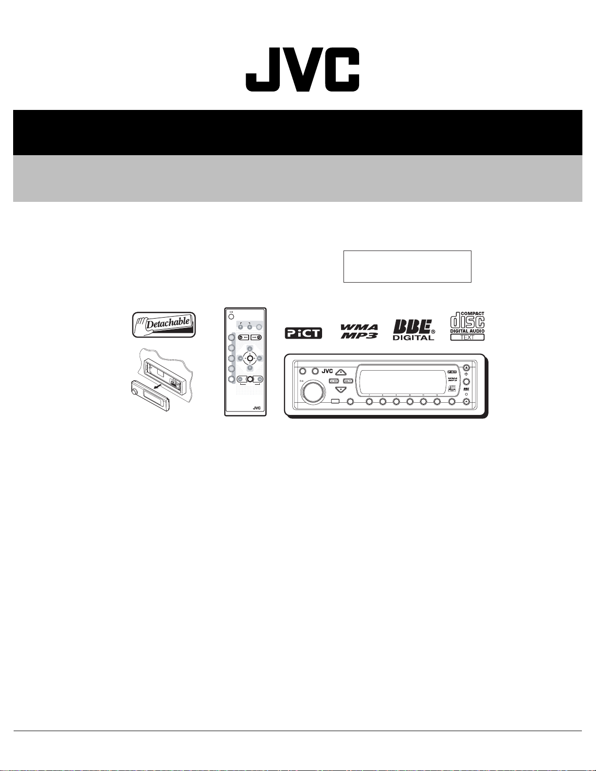
SERVICE MANUAL
CD RECEIVER
4983420036
KD-SH9105
Area Suffix
U -------------------- Other Areas
ATT
ANGLE
EQ
CD
DAB
DISC
FM
PRESET
PRESET
R D
AM
CH
AUX SEL
RM-RK100
50Wx4
SRC
DISC
VOLUME
D
DISP
ATT
MOSFET
SEL
KD-SH9105
BBE
3456 M21
MODE
TABLE OF CONTENTS
1 PRECAUTION. . . . . . . . . . . . . . . . . . . . . . . . . . . . . . . . . . . . . . . . . . . . . . . . . . . . . . . . . . . . . . . . . . . . . . . . . 1-3
2 SPECIFIC SERVICE INSTRUCTIONS. . . . . . . . . . . . . . . . . . . . . . . . . . . . . . . . . . . . . . . . . . . . . . . . . . . . . . 1-5
3 DISASSEMBLY . . . . . . . . . . . . . . . . . . . . . . . . . . . . . . . . . . . . . . . . . . . . . . . . . . . . . . . . . . . . . . . . . . . . . . . 1-6
4 ADJUSTMENT . . . . . . . . . . . . . . . . . . . . . . . . . . . . . . . . . . . . . . . . . . . . . . . . . . . . . . . . . . . . . . . . . . . . . . . 1-27
5 TROUBLE SHOOTING. . . . . . . . . . . . . . . . . . . . . . . . . . . . . . . . . . . . . . . . . . . . . . . . . . . . . . . . . . . . . . . . . 1-32
6 Description of major ICs. . . . . . . . . . . . . . . . . . . . . . . . . . . . . . . . . . . . . . . . . . . . . . . . . . . . . . . . . . . . . . . 1-33
COPYRIGHT © 2003 VICTOR COMPANY OF JAPAN, LIMITED
No.49834
2003/6
Page 2
SPECIFICATION
AUDIO AMPLIFIER SECTION Maximum Power Output Front 50 W per channel
Rear 50 W per channel
Continuous Power Output (RMS) Front 19 W per channel into 4 Ω, 40 Hz
to 20 000 Hz at no more than 0.8%
total harmonic distortion.
Rear 19 W per channel into 4 Ω, 40 Hz
to 20 000 Hz at no more than 0.8%
total harmonic distortion.
Load Impedance 4 Ω (4 Ω to 8 Ω allowance)
Equalizer Control Range Frequencies 60 Hz, 150 Hz, 400 Hz, 1 kHz, 2.4
kHz, 6 kHz, 12 kHz
Level ±10 dB
Frequency Response 40 Hz to 20 000 Hz
Signal-to-Noise Ratio 70 dB
Line-In Level/Impedance LINE IN 1.5 V/20 kΩ load
Line-Out Level/Impedance LINE OUT 4.0 V/20 kΩ load (full scale)
Output Impedance 1 kΩ
TUNER SECTION Frequency Range FM 87.5 MHz to 108.0 MHz
AM 531 kHz to 1 602 kHz
[FM Tuner] Usable Sensitivity 11.3 dBf (1.0 µV/75 Ω)
50 dB Quieting Sensitivity 16.3 dBf (1.8 µV/75 Ω)
Alternate Channel Selectivity
(400 kHz)
Frequency Response 40 Hz to 15 000 Hz
Stereo Separation: 35 dB
Capture Ratio 1.5 dB
[AM Tuner] Sensitivity 20 µV
Selectivity 35 dB
CD PLAYER SECTION Type Compact disc player
Signal Detection System Non-contact optical pickup (semiconductor laser)
Number of channels 2 channels (stereo)
Frequency Response 5 Hz to 20 000 Hz
Dynamic Range 98 Db
Signal-to-Noise Ratio 102 dB
Wow and Flutter Less than measurable limit
MP3 (MPEG Audio Layer 3) Max.
Bit rate:
WMA (Windows Media® Audio)
Max. Bit rate:
GENERAL Power Requirement Operating Voltage DC 14.4 V (11 V to 16 V allowance)
Grounding System Negative ground
Allowable Operating Temperature 0°C to +40°C
Dimensions (W × H × D) Installation Size 182 mm × 52 mm × 161 mm
Panel Size 188 mm × 58 mm × 17 mm
Mass 1.8 kg (excluding accessories)
320 Kbps
192 Kbps
65 dB
1-2 (No.49834)
Page 3
1.1 Safety Precautions
SECTION 1
PRECAUTION
!
!
Burrs formed during molding may be left over on some parts of the chassis. Therefore,
pay attention to such burrs in the case of preforming repair of this system.
Please use enough caution not to see the beam directly or touch it in case of an
adjustment or operation check.
(No.49834)1-3
Page 4
1.2 Preventing static electricity
Electrostatic discharge (ESD), which occurs when static electricity stored in the body, fabric, etc. is discharged, can destroy the laser
diode in the traverse unit (optical pickup). Take care to prevent this when performing repairs.
1.2.1 Grounding to prevent damage by static electricity
Static electricity in the work area can destroy the optical pickup (laser dio de) in devices such as CD players.
Be careful to use proper grounding in the area where repairs are being performed.
(1) Ground the workbench
Ground the workbench by laying conductive material (such as a conductive sh eet) or an iron plate over it before placing the
traverse unit (optical pickup) on it.
(2) Ground yourself
Use an anti-static wrist strap to release any static electricity built up in your body.
(caption)
Anti-static wrist strap
1M
Conductive material
(conductive sheet) or iron plate
(3) Handling the optical pickup
• In order to maintain quality during transport and before instal lation, both sides of the laser di ode on the replacement optica l
pickup are shorted. After replacement, return the shorted parts to their original condition.
(Refer to the text.)
• Do not use a tester to check the condition of the laser diode in the optical pickup. The tester's internal power source can easily
destroy the laser diode.
1.3 Handling the traverse unit (optical pickup)
(1) Do not subject the traverse unit (optical pickup) to strong shocks, as it is a sensitive, complex unit.
(2) Cut off the shorted part of the flexible cable using nippers, etc. after replacing the optical pickup. For specific details, refer to the
replacement procedure in the text. Remove the anti-static pin when replacing the traverse unit. Be careful not to take too long a
time when attaching it to the connector.
(3) Handle the flexible cable carefully as it may break when subjected to strong force.
(4) It is not possible to adjust the semi-fixed resistor that adjusts the laser power. Do not turn it.
1.4 Attention when traverse unit is decomposed *Please refer to "Disassembly method" in the text for the CD pickup unit.
• Apply solder to the short land before the flexible wire is disconnected from the connector on the CD pickup unit.
(If the flexible wire is disconnected without applying solder, the CDpickup may be destroyed by static electricity.)
• In the assembly, be sure to remove solder from the short land after connecting the flexible wire.
Short-circuit point
(Soldering)
Flexible wire
1-4 (No.49834)
Pickup
Page 5

SECTION 2
SPECIFIC SERVICE INSTRUCTIONS
This service manual does not describe SPECIFIC SERVICE INSTRUCTIONS.
(No.49834)1-5
Page 6
SECTION 3
DISASSEMBLY
3.1 Main body section
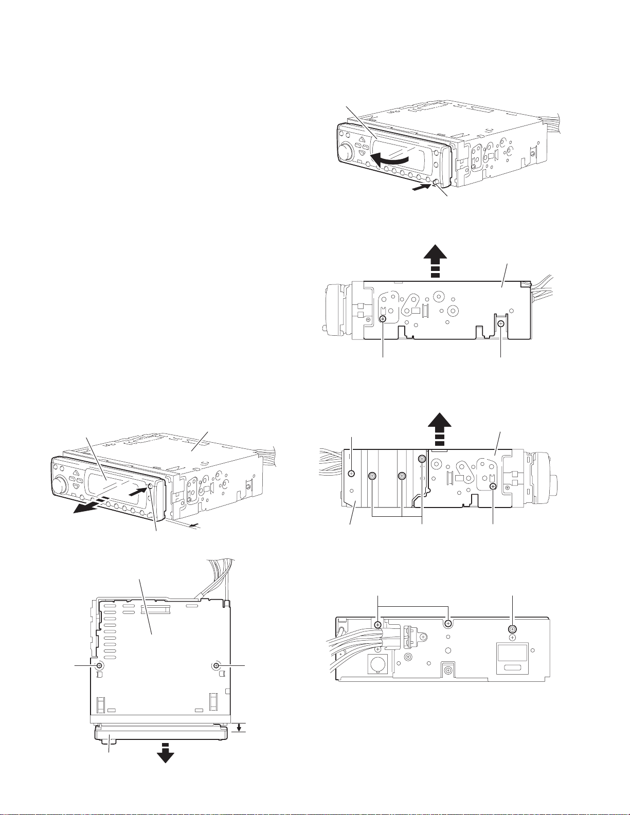
3.1.1 Removing the front panel assembly
(See Fig.1)
(1) Push the detach button in the lower right part of the front
panel assembly.
(2) Remove the front panel assembly in the direction of the arrow .
3.1.2 Removing the top chassis
(See Figs.2 to 6)
• Turn on power.
(1) Push the eject button in the upper right part of the front pan-
el assembly to move the front panel assembly as shown in
Fig.2 and turn off power.
(2) Remove the two screws A attaching the top chassis from
the top side of the main body. (See Fig.3.)
(3) Remove the three screws B attaching the top chassis from
the both sides of the main body. (See Figs.4 and 5.)
(4) Remove the screw C and three screws D attaching the heat
sink from the left side of the main body. (See Fig.5.)
(5) Remove the two screws E and screw F attaching the top
chassis from the back side of the main body. (See Fig.6 .)
(6) Move the top chassis up ward and remove it with the CD
mechanism assembly. The connector CN501 on the CD
mechanism assembly is disconnected from the connector
CN981 on the main board.
Front panel assembly
Top chassis
Front panel assembly
BB
C
Detach button
Fig.1
Top chassis
Fig.4
Top chassis
A
Front panel assembly
1-6 (No.49834)
Eject button
Fig.2
Top chassis
Fig.3
A
Heat sink
E
BD
Fig.5
F
Fig.6
Page 7
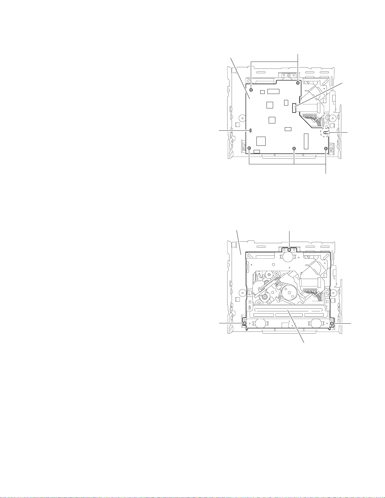
3.1.3 Removing the mecha control board
(See Fig.7)
• Prio r to performing the following procedures, remove the top
chassis.
(1) Disconnect the card wire from the connector CN601 on the
mecha control board.
(2) Remove the five screws G attaching the mecha control
board.
(3) Release the joints a and b, remove the mecha control
board.
Mecha control board
G
CN601
3.1.4 Removing the CD mechanism assembly
(See Fig.8)
• Prio r to performing the following procedure, remove the top
chassis.
(1) Remove the three screws H from the inside of the top chas-
sis and remove the CD mechanism assembly.
a
Top chassis
b
G
Fig.7
H
HH
CD mechanism assembly
Fig.8
(No.49834)1-7
Page 8
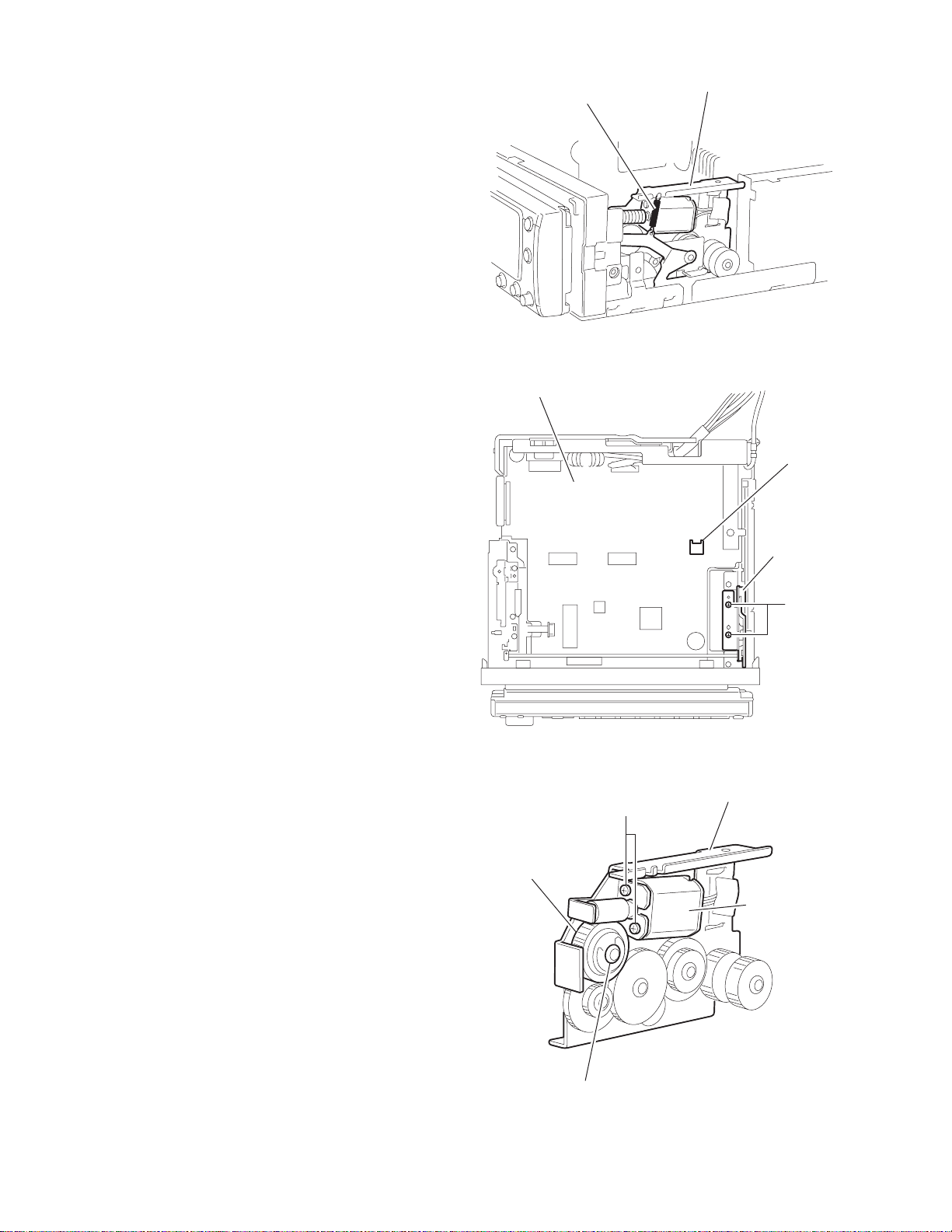
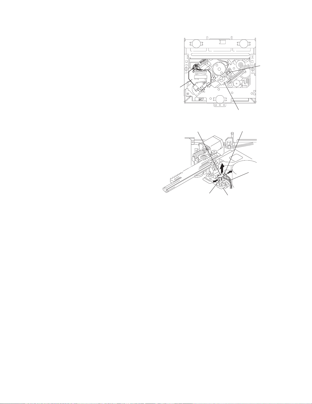
3.1.5 Removing the motor assembly
(See Figs.9 to 11)
• Prior to performing the following procedures, remove the top
chassis.
(1) Remove the spring from the motor bracket. (See Fig.9.)
(2) Disconnect the wire from the connector CN982 on the main
board. (See Fig.10.)
(3) Remove the two screws J attaching the motor bracket.
(See Fig.10.)
(4) Remove the washer attaching the clutch assembly and pull
out the clutch assembly from the shaft. (See Fig.11.)
(5) Remove the two screws K attaching the motor assembly to
the motor bracket. (See Fig.11.)
Main board
Spring
Motor braket
Fig.9
CN982
Clutch assembly
Motor braket
J
Fig.10
Motor braket
K
Motor assembly
1-8 (No.49834)
Washer
Fig.11
Page 9
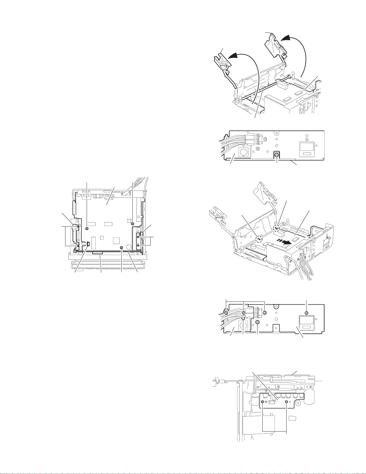
3.1.6 Removing the main board
k
(See Figs.12 to 16)
• Prio r to performing the following procedures, remove the top
chassis and motor assembly.
(1) Disconnect the flexible wires from the con nectors CN703
and CN991 on the main board respectively. (See Fig.12.)
(2) Move the front bracket backward until it stops.
(3) Remove the four screws L attaching the arm brackets (L)
and (R). Move the arm brackets (L) and (R) from the rod
gear. (See Fig.12.)
(4) Remove the rod gear.
(5) Remove the screw M attaching the rear panel to the bottom
cover from the back side of the main body. (See Fig.14.)
(6) Remove the three screws N attaching the main b oard and
move the main board backwards to release the two joints
c. (The main board will be removed with the rear panel and
rear heat sink) (See Figs.12 and 15.)
(7) Remove the screw P and Q attaching the rear he at sink.
(See Fig.16.)
(8) Remove the three screws R and screw S attaching the rear
panel, then remove the main board. (See Fig.16.)
NN
Main board
Arm
brackets (L)
L
Arm
brackets (R)
Arm brackets (L)
Arm brackets (R)
Rod gear
Rear panel
Joint c
Fig.13
M
Fig.14
Main board
Bottom cover
Joint c
Main board
L
CN703
3.1.7 Removing the lifter switch board
(See Fig.17)
• Prio r to performing the following procedure, remove the top
chassis, motor assembly and main board.
(1) Remove the two screws T attaching the lifter switch board
to the bottom chassis.
CN991
Fig.12
M
Rod gear
R
Rear panel
Lifter switch board
S
Q
Fig.15
P
Rear heat sin
Fig.16
Bottom chassis
T
Fig.17
(No.49834)1-9
Page 10
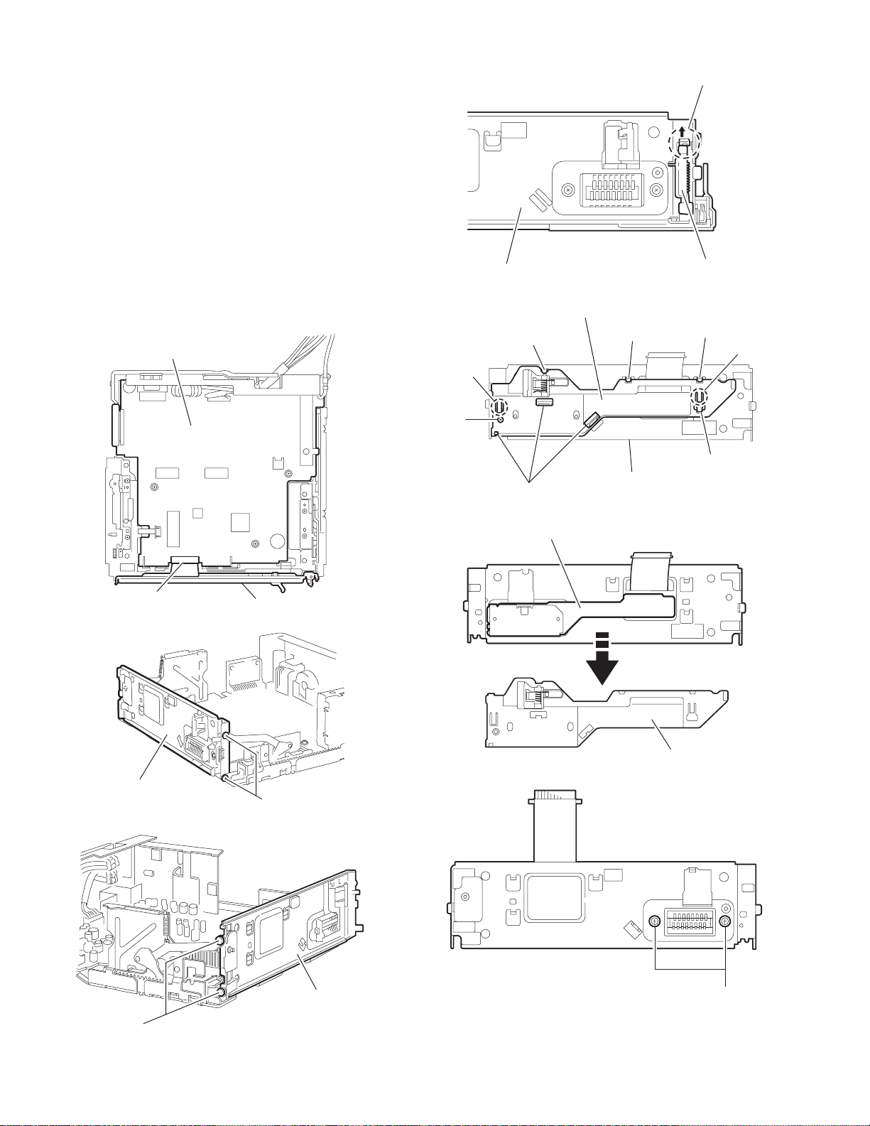
3.1.8 Removing the lifter board
(See Figs.18 to 24)
• Prior to performing the following procedures, remove the top
chassis and front panel assembly.
(1) Disconnect the flexible wire from the connector CN991 on
the main board. (See Fig.18.)
(2) Remove the four screws U attaching the front bracket on
the both sides of the main body. (See Figs.19 and 20.)
(3) Push the pin of the joint d on the front side of the front
bracket to release the detach lever. (See Fig.21.)
(4) Remove the screw V attaching the connector cover in the
rear side of the front bracket. (See Fig.22.)
(5) Release the two joints f while pushing them from the front
side, and then move the connector cover in the direction of the
arrow and release the eight joints e. (See Figs.22 and 23.)
(6) Remove the two screws W attach ing the lifter board from
the front side of the main body. (See Fig.24.)
Main board
Front bracket
Joint f
V
Connector cover
Joint e
Joints e
Lifter board
Fig.21
Joint
Front bracket
Fig.22
e
d
Joint
Datch lever
Joint e
Joint f
Joint e
CN991
Front bracket
U
Fig.18
Fig.19
Fig.20
Front bracket
U
Front bracket
Connector cover
Fig.23
W
Fig.24
1-10 (No.49834)
Page 11
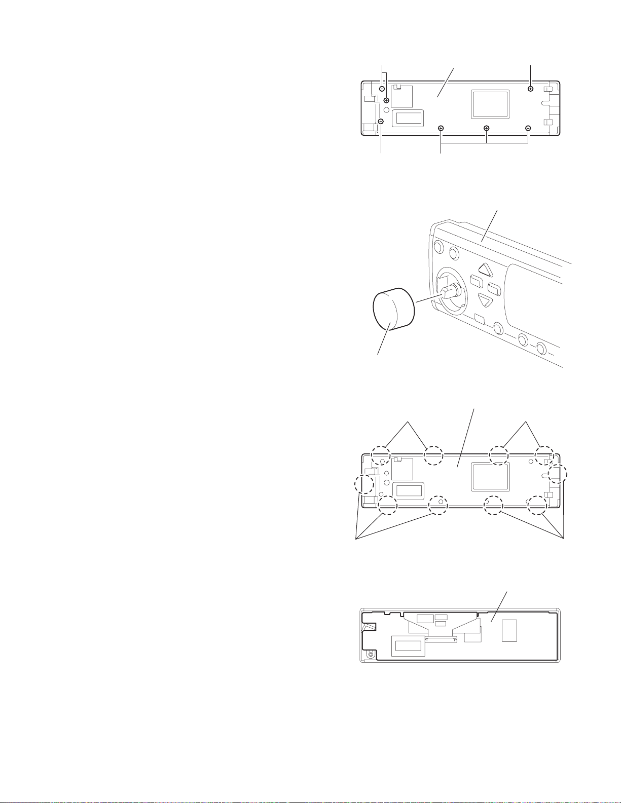
3.1.9 Removing the front board (See Figs.25 to 28)
• Prio r to performing the following procedure s, remove the front
panel assembly.
(1) Remove the six screws X attaching the rear panel to the
front panel assembly. (See Fig.25.)
(2) Pull out the volume knob from the front side of the front
panel assembly. (See Fig.26.)
(3) Release the ten joints g of the front panel and the rear pan-
el. (See Fig.27.)
(4) Take out the front bo ard from the front panel assembly.
(See Fig.28.)
XX
Rear panel
XX
Fig.25
Front panel assembly
Volume knob
Joints g
Joints g
Fig.26
Rear panel
Joints g
Joints g
Fig.27
Front board
Fig.28
(No.49834)1-11
Page 12
3.2 CD Mechanism section
A
3.2.1 Removing the top cover
(See Figs.1 and 2)
(1) Remove the four screws A on the both side of the body.
(2) Lift the front side of the top cover and move the top cover
backward to release the two joints a.
Top cover
Joints a
A
Joints a
A
Fig.1
Fig.2
Top cover
1-12 (No.49834)
Page 13
3.2.2 Removing the connector board
(See Figs.3 to 5)
CAUTION:
Before disconnecting the flexible wire from the pickup, solder
the short-circuit point on the pickup. No observance of this instruction may cause damage of the pickup.
(1) Remove the screw B fixing the connector board.
(2) Solder the short-circuit point on the pickup.
(3) Disconnect the flexible wire from the pickup.
(4) Move the connector board in the direction of the arrow to
release the two joints b.
(5) Unsolder the wires on the connector bo ard if necessary.
CAUTION:
Unsolder the short-circuit point after reassembling.
B
Connector board
Flexible wire
Wires
Joints b
Short-circuit point
Fig.3
Short-circuit point
(Soldering)
Pickup
Flexible wire
Frame
Pickup
Fig.4
B
Connector board
Fig.5
(No.49834)1-13
Page 14
3.2.3 Removing the DET switch
(See Figs.6 and 7)
(1) Extend the two tabs c of the feed sw. holder and pull out
the switch.
(2) Unsolder the DET switch wire if necessary.
DET
switch
Connector
board
Pickup
Fig.6
DET switch
Tab c
Tab c
DET switch wire
Feed sw. holder
Fig.7
1-14 (No.49834)
Page 15

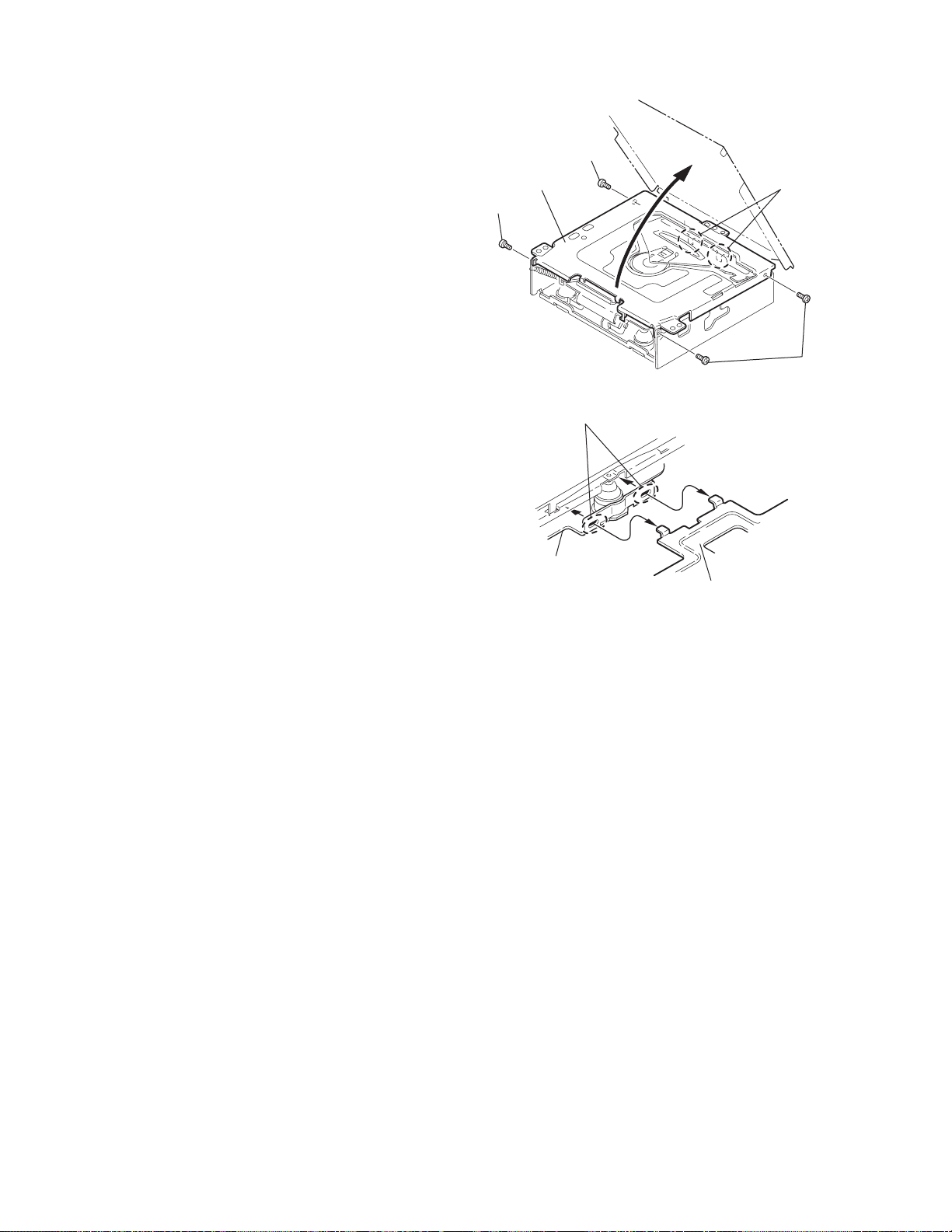
3.2.4 Removing the chassis unit
r
(See Figs.8 and 9)
• Prio r to performing the following procedure, remove the top
cover and connector board.
(1) Remove the two suspensi on springs (L) an d (R) attaching
the chassis unit to the frame.
CAUTION:
• The shape of the suspension spring (L) and (R) are different. Handle them with care.
• W hen reassembling, make sure that the three shafts
on the underside of the chassis unit are inserted to the
dampers certainly.
Suspension spring (R)
Chassis unit
Suspension spring (L)
Frame
Suspension spring (R)
Chassis unit
Shafts
Damper
Damper
Suspension spring (L)
Fig.8
Shaft
Dampe
Frame
Fig.9
(No.49834)1-15
Page 16

3.2.5 Removing the clamper assembly
(See Figs.10 and 11)
• Prior to performing the following procedure, remove the top
cover.
(1) Remove the clamper arm spring.
(2) Move the clamper assembly in the direction of the arrow to
release the two joints d.
Clamper arm
spring
Joint d
Joint d
Clamper assembly
Fig.10
Clamper arm spring
Chassis rivet
assembly
Joint d
Clamper assembly
Chassis rivet assembly
Joint d
Fig.11
1-16 (No.49834)
Page 17

3.2.6 Removing the loading / feed motor assembly
(See Figs.12 and 13)
• Prio r to performing the following procedure, remove the top
cover, connector board and chassis unit.
(1) Remove the screw C and move the loading / feed motor as-
sembly in the direction of the arrow to remove it from the
chassis rivet assembly.
(2) Disconnect the wire from the loading / feed motor assembly
if necessary.
CAUTION:
When reassembling, connect the wire from the loading /
feed motor assembly to the flame as shown in Fig.12.
Loading / feed motor assembly
Fig.12
Loading / feed motor assembly
C
Fig.13
(No.49834)1-17
Page 18

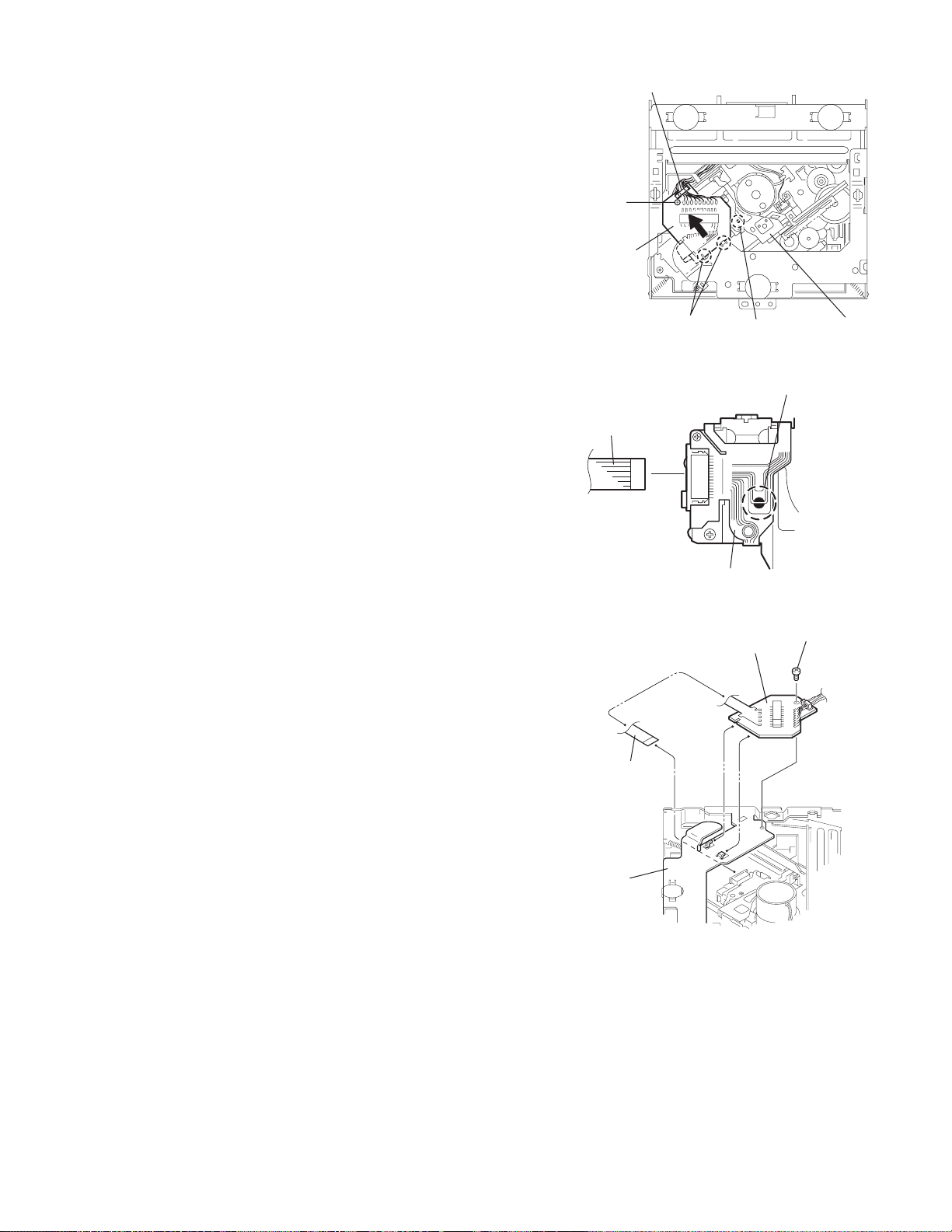
3.2.7 Removing the pickup unit
r
(See Figs.14 to 18)
• Prior to performing the following procedure, remove the top
cover, connector board and chassis unit.
(1) Remove the screw D and pull out the pu. shaft holder from
the pu. shaft.
(2) Remove the screw E attaching the feed sw. holder.
(3) Move the part e of the pickup unit upward with the pu. shaft
and the feed sw. holder, then release the joint f of the feed
sw. holder in the direction of the arrow. The joint g of the
pickup unit and the feed rack is released, and the feed sw.
holder comes off.
(4) Remove the pu. shaft from the pickup unit.
(5) Remove the screw F attaching the feed rack to the pickup
unit.
3.2.8 Reattaching the pickup unit
(See Figs.14 to 17)
(1) Reattach the feed rack to the pickup unit using the screw F.
(2) Reattach the feed sw. holder to the feed rack wh ile setting
the joint g to the slot of the feed rack and setting the joint f
of the feed rack to the switch of the feed sw. holder correctly.
(3) As the feed sw. holder is temporarily attached to the pickup
unit, set to the gear of the joint g and to the bending part of
the chassis (joint h) at a time.
CAUTION:
Make sure that the part i on the underside of the feed
rack is certainly inserted to the slot j of the change lock
lever.
(4) Reattach the feed sw. holder using the screw E.
(5) Reattach the pu. shaft to the pickup unit. Reattach the pu.
shaft holder to the pu. shaft using the screw D.
Part e
Joint g
Feed sw. holder
Feed rack
Part i
E
Slot j
F
Feed sw. holder
Fig.15
Pu. shaft
Pickup unit
Joint f
Joint h
Fig.16
Feed rack
Pickup unit
D
Pu. shaft holde
Joint f
Pu. shaft
D
Pu. shaft holder
Feed sw. holder
Pickup unit
Fig.14
Part e
E
Joint g
Pickup unit
Feed rack
Fig.17
Pickup unit
Joint g
Joint f
Feed sw. holder
Fig.18
1-18 (No.49834)
Page 19

3.2.9 Removing the trigger arm
r
(See Figs.19 and 20)
• Prio r to performing the following procedure, remove the top
cover, connector board and clamper unit.
(1) Turn the trigger arm in the direction of the arrow to release
the joint k and pull out upward.
CAUTION:
When reassembling, insert the part m and n of the trigger
arm into the part p and q at the slot of the chassis rivet
assembly respectively and join the joint k at a time.
Chassis rivet assembly
Trigger arm
Chassis
rivet
assembly
Joint k
Trigger arm
Fig.19
Part p
Part q
Part m
Part n
3.2.10 Removing the top plate assembly
(See Fig.21)
• Prio r to performing the following procedure, remove the top
cover, connector board, chassis unit, and clamper assembly.
(1) Remove the screw H.
(2) Move the top plate assembly in the direction of the arrow to
release the two joints r.
(3) Unsolder the wire marked s if necessary.
H
Fig.20
Top plate assembly
Joints
s
Fig.21
(No.49834)1-19
Page 20

3.2.11 Removing the mode sw. / select lock arm
(See Figs.22 and 23)
• Prior to performing the following procedure, remove the top
plate assembly.
(1) Bring up the mode sw. to release from the link plate (joint t)
and turn in the direction of the arrow to release the joint u.
(2) Unsolder the wire of the mode sw. marked s if necessary.
(3) Turn the select lock arm in the direction of the arrow to re-
lease the two joints v.
(4) The select lock arm spring comes off the select lock arm at
the same time.
Link plate
Joint u
Fig.22
Joint t
Mode sw.
Select lock arm
s
Top plate
Select lock arm
Link plate
Select lock arm
Fig.23
Top plate
Hook w
Select lock
arm spring
Joints v
1-20 (No.49834)
Page 21

3.2.12 Reassembling the mode sw. / select lock arm
(See Figs.24 to 26)
REFERENCE:
Reverse the above removing procedure.
(1) Reattach the select lock arm spring to the top plate and set
the shorter end of the select lock arm spring to the hook w
on the top plate.
(2) Set the other longer end of the select lock arm spring to the
boss x on the underside of the select lock arm, and join the
select lock arm to the slots (joint v). Turn the select lock
arm as shown in the figure.
(3) Reattach the mode sw. while setting th e part t to the first
peak of the link plate gear, and join the joint u.
CAUTION:
When reattaching the mode sw., check if the points y and
z are correctly fitted and if each part operates properly.
Select lock arm spring
Hook w
Joint v
Joint v
Select lock arm
Boss x
Fig.24
Joint t
Point y
Link plate
Point z
Link plate
Fig.25
Mode sw.
Select
lock arm
Joint t
Joint u
Fig.26
(No.49834)1-21
Page 22

3.2.13 Removing the select arm R / link plate
(See Figs.27 and 28)
• Prior to performing the following procedure, remove the top
plate assembly.
(1) Bring up the select arm R to release from the link plate
(joint a') and turn as shown in the figure to release the two
joints b' and joint c'.
(2) Move the link plate in the direction of the arrow to release
the joint d'. Remove the link plate spring at the same time.
REFERENCE:
Before removing the link plate, remove the mode sw..
Select arm R
Joint b'
Link plate spring
Joint c'
Joint a'
Link plate
Joint b'
Fig.27
Joint r
3.2.14 Reattaching the Select arm R / link plate
(See Figs.29 and 30)
REFERENCE:
Reverse the above removing procedure.
(1) Reattach the link plate spring.
(2) Reattach the link plate to th e lin k plate sprin g whil e joi ning
them at joint d'.
(3) Reattach the joint a' of the select arm R to the first peak of
the link plate while joining the two joints b' with the slots.
Then turn the select arm R as shown in the figure. The top
plate is joined to the joint c'.
CAUTION:
When reattaching the select arm R, check if the points e'
and f' are correctly fitted and if each part operates properly.
Top plate
Select arm R
Joint b'
Joint d'
Link plate
Fig.28
Link plate spring
Joint c'
Joint d'
Joint b'
Joint a'
Fig.29
1-22 (No.49834)
Joint a'
Point e'
Link plate
Point f'
Fig.30
Page 23

3.2.15 Removing the loading roller assembly
(See Figs.31 to 33)
• Prior to performing the following procedure, remove the
clamper assembly and top plate assembly.
(1) Push inward the loading roller assembly on the gear side
and detach it upward from the slot of the joint g' of the lock
arm rivet assembly.
(2) Detach the loading roller assembly from the slot of the joint
h' of the lock arm rivet assembly.
The roller guide comes off the gear section of the loading
roller assembly.
Remove the roller guide and the HL washer from the shaft
of the loading roller assembly.
(3) Remove the screw J attaching the lock arm rivet assembly.
(4) Push the shaft at the joint i' of the lock arm rivet assembly
inward to release the lock arm rivet assembly from the slot
of the L side plate.
(5) Extend the lock arm rivet assembly outward and release
the joint j' from the boss of the chassis rivet assembly. The
roller guide springs on both sides come off at the same
time.
CAUTION:
When reassembling, reattach the left and right roller
guide springs to the lock arm rivet assembly before reattaching the lock arm rivet assembly to the chassis rivet
assembly. Make sure to fit the part k' of the roller guide
spring inside of the roller guide. (Refer to Fig.34.)
Roller guide
spring
Part k'
Chassis rivet assembly
Loading roller assembly
Loading roller assembly
Roller guide
spring
Fig.32
Boss
Roller guide
Joint h'
Roller guide spring
Loading roller assembly
HL washer
Loading roller assembly
Joint g'
Lock arm rivet assembly
Fig.31
Roller guide
Roller guide spring
Roller guide spring
J
Lock arm rivet assembly
Lock arm rivet assembly
L side plate
Roller guide spring
Joint i'
Joint j'
Fig.33
Roller guide
HL washer
Roller shaft assembly
Loading roller
Roller guide spring
Fig.34
(No.49834)1-23
Page 24

3.2.16 Removing the loading gear 5, 6 and 7
(See Figs.35 and 36)
• Prior to performing the following procedure, remove the top
cover, chassis unit, pickup unit and top plate assembly.
(1) Remove the screw K attaching the loading gear bracket.
The loading gear 6 and 7 come off the loading gear bracket.
(2) Pull out the loading gear 5.
K
Loading gear 5
Loading gear bracket
K
Loading gear 6
Loading gear 5
Loading gear 3
Fig.35
Loading gear bracket
Loading gear 6
Loading gear 7
Fig.36
1-24 (No.49834)
Page 25

3.2.17 Removing the gears
(See Figs.37 to 40)
• Prio r to performing the following procedure, remove the top
cover, chassis unit, top plate assembly and pickup unit.
• Pull out the loading gear 3. (See Fig.35.)
(1) Pull out the feed gea r.
(2) Move the loading plate a ssemb ly in the d irection o f the ar-
row to release the L side plate from the two slots m' of the
chassis rivet assembly. (See Fig.37.)
(3) Detach the loading plate assemb ly upward from the chas-
sis rivet assembly while releasing the joint n'. Remove the
slide hook and loading plate spring from the loading plate
assembly.
(4) Pull out the loading gear 2 and remove the change lock le-
ver.
(5) Remove the E ring and washer attaching the change gear
2.
(6) The change gear 2, change gear spring and adjusting
washer come off.
(7) Remove the loading gear 1.
(8) Move the change plate rivet assembly in the direction of the
arrow to release from the three shafts of the chassis rivet
assembly upward. (See Fig.38.)
(9) Detach the loading gear plate rivet assembly from the shaft
of the chassis rivet assembly upward while releasing the
joint p'. (See Figs.38 and 40.)
(10) Pull out the loading gear 4.
Change plate
rivet assembly
Shafts
E ring
Loading plate assembly
Loading plate spring
Joint p'
Loading gear 4
Loading gear plate
rivet assembly
Shaft
Loading gear 2
Loading gear 1
Chassis rivet assembly
Change gear 2
Fig.38
Joint n'
Slide hook
Feed gear
Fig.37
Slot m'
L side plate
Loading plate assembly
Joint n'
Slot m'
Chassis rivet assembly
Chassis rivet assembly
E ring
Washer
Change gear 2
Change gear
spring
Adjusting
washer
Change plate
rivet assembly
L side plate
Slot m'
Slot m'
Fig.39
Loading gear 1
Loading gear 2
Change lock lever
Loading gear 4
Chassis rivet assembly
Loading gear plate rivet
assembly
Fig.40
(No.49834)1-25
Page 26

3.2.18 Removing the turn table / spindle motor
(See Figs.41 and 42)
• Prior to performing the following procedure, remove the top
cover, connector board, chassis unit and clamper assembly.
(1) Remove the two screws L attaching the spindle motor as-
sembly through the slot of the turn table on top of the body.
(2) Unsolder the wire on the connector board if necessary.
Turn table
L
Fig.41
L
Turn table
1-26 (No.49834)
Spindle motor
Fig.42
Page 27

SECTION 4
le
ADJUSTMENT
4.1 Adjustment method Test instruments required for adjustment
(1) Digital oscilloscope (100MHz)
(2) AM Standard signal generator
(3) FM Standard signal generator
(4) Stereo modulator
(5) Electric voltmeter
(6) Digital tester
(7) Tracking offset meter
(8) Test Disc JVC :CTS-1000
(9) Extension cable for check
EXTSH002-22P × 1
Standard volume position
Balance and Bass &Treble volume : lndication"0"
Loudness : OFF
How to connect the extension cable for adjusting
Caution:
Be sure to attach the heat sink and rear bracket onto the power amplifier IC and regulator IC respectively, before supply the power.
If voltage is applied without attaching these parts, the power amplifier IC and regulator IC will be destroyed by heat.
Standard measuring conditions
Power supply voltage DC14.4V(11 to 16V)
Load impedance 20KΩ(2 Speakers connection)
Output Level Line out 2.0V (Vol. MAX)
Dummy load
Exclusive dummy load should be used for AM,and FM. For FM
dummy load,there is a loss of 6dB between SSG output and
antenna input.The loss of 6dB need not be considered since
direct reading of figures are applied in this working standard.
Extension cab
EXTSH002-22P
(No.49834)1-27
Page 28

4.2 Service mode
When entering the service mode, "DATA CLEAR" is displayed without fail.
: Initial display
SEL
POWER
SOURCE
A
DATA_CLEAR
DISC+/-:CATEGORY
: SEEK UP
: SEEK DOWN
: DISC UP
: DISC DOWN
EPROM_CLEAR
NAME_CLEAR
CD_ERROR_CLEAR
CH_ERROR_CLEAR
SH_MECHA_ERROR_CLEAR
EPROM_CLEAR
NAME_CLEAR
CD_ERROR_CLEAR
CH_ERROR_CLEAR
SH_MECHA_ERROR_CLEAR
EPROM_CLEAR
NAME_CLEAR
CD_ERROR_CLEAR
CH_ERROR_CLEAR
SH_MECHA_ERROR_CLEAR
EPROM_CLEAR
NAME_CLEAR
CD_ERROR_CLEAR
CH_ERROR_CLEAR
SH_MECHA_ERROR_CLEAR
EPROM_CLEAR
NAME_CLEAR
CD_ERROR_CLEAR
CH_ERROR_CLEAR
SH_MECHA_ERROR_CLEAR
PICTURE_CLEAR
DSP_ERROR_CLEAR
PICTURE_CLEAR
DSP_ERROR_CLEAR
___NOW
___ERROR_CLEAR
SEL
*Letter turn on and off
(Turn on: 0.5sec, Turn off: 0.5sec)
___NOW
___NAME_CLEAR
SEL
*Letter turn on and off
(Turn on: 0.5sec, Turn off: 0.5sec)
___NOW
___CD_ERROR_CLEAR
SEL
*Letter turn on and off
(Turn on: 0.5sec, Turn off: 0.5sec)
___NOW
___CH_ERROR_CLEAR
SEL
*Letter turn on and off
(Turn on: 0.5sec, Turn off: 0.5sec)
___NOW
___SH_MECHA_ERROR_CLEAR
SEL
*Letter turn on and off
(Turn on: 0.5sec, Turn off: 0.5sec)
___NOW
___PICTURE_CLEAR
SEL
*Letter turn on and off
(Turn on: 0.5sec, Turn off: 0.5sec)
___NOW
___DSP_ERROR_CLEAR
SEL
*Letter turn on and off
(Turn on: 0.5sec, Turn off: 0.5sec)
EPROM all clear & Flash ROM all clear
(Following all contents are cleared.)
Execute by "SEL" key
Normal
display
EPROM (DISC/LINE NAME) clear
Execute by "SEL" key
Normal
display
EPROM (CD ERROR) clear
Execute by "SEL" key
Normal
display
EPROM (CH ERROR) clear
Execute by "SEL" key
Normal
display
EPROM (SH DOOR MECHA ERROR) clear
Execute by "SEL" key
Normal
display
Flash ROM (all PICTURE) clear
Execute by "SEL" key
Normal
display
Flash ROM (all DSP retry count number) clear
Execute by "SEL" key
Normal
display
RUNNING_MODE
DISC+/-:FUNCTION
B
C
1-28 (No.49834)
RUNNING_CD
RUNNING_SH_MECHA
RUNNING_CD
RUNNING_SH_MECHA
RUNNING_CD
COUNT :
ERROR :
SEL
RUNNING_SH_MECHA
COUNT :
ERROR :
SEL
CD running mode (SH mecha open)
Running number
CD error during running mode
by error code chart
Door mecha running mode (No retry action)
Running number
Door error during running mode
by error code chart
Page 29

B
C
CD_DATA_READ
DISC+/-:FUNCTION
ERROR_READ
DISC+/-:FUNCTION
ADJ_NOW
ADJ_INT
OTHERS
ADJ_NOW
ADJ_INT
OTHERS
ADJ_NOW
ADJ_INT
OTHERS
CD_ERROR_READ
CH_ERROR_READ
SH_MECHA_ERROR_READ
CD_ERROR_READ
CH_ERROR_READ
SH_MECHA_ERROR_READ
ADJ_NOW
FEB__ ____TEB__
FGA__ ____TGA__
SEL
FEO__ ____RFG__
TEO__
ADJ_INT
FEB__ ____TEB__
FGA__ ____TGA__
SEL
FEO__ ____RFG__
TEO__
OTHERS
IOP__TEMP____I T
IOP__INT__
SEL
TEMP__MAX__
P_TOTAL_ H
TOTAL_ERROR :
E1_ _____2_
E2_ _____3_
SEL
E3_ _____4_
1__ 5_
TOTAL_ERROR :
E1_ _____2_
E2_ _____3_
SEL
E3_ _____4_
1__ 5_
CD data display
Hex. code display
Total running time display
(Four figures (to 9999), hour only, omit)
CD error display
Total error number
Display by error code chart
CH error display
Total error number
Display by error code chart
VERSION
MAIN_V
CD_V
CH_V
A
CD_ERROR_READ
CH_ERROR_READ
SH_MECHA_ERROR_READ
CD_ERROR_READ
CH_ERROR_READ
SH_MECHA_ERROR_READ
E1_
E2_
SEL
E3_
1__
INIT_RETRY____TOTAL_
INIT_RETRY_NG_TOTAL_
SEL
SH door mecha error display
Display by error code chart
DSP initial setting data error
Retry total number of initial setting
Error number: NG after retry two times
(First transmit NG Retry first transmit NG
Second transmit NG : 1 count)
(No.49834)1-29
Page 30

4.3 Flow of functional operation unit TOC read
When the pickup correctly moves
to the inner area of the disc
$82
Microprocessor
commands
FMO
TC94A14FA "40"
FEED MOTOR
+TERMINAL
IC681 "17"
REST SW
When correctly focused
FEO
TA2157 "15"
$83
$81
Focus Servo Loop ONo
v
3.3V
Hi-Z
0V
6V
4V
2V
OFF
ON
Pickup feed to the inner area
2.2V
RF signal eye-pattern
remains closed
RF signal eye-pattern
opens
Power ON
Set Function CD
Disc inserted
YES
Laser emitted
Focus search
Disc rotates
n
Tracking loop closed
TOC read out
YES
When the laser diode correctly
emits
Microprocessor
commands
SEL
TC94A14FA "38"
LD
CN601 "10"
"No disc"
display
When the disc correctly rotates
Microprocessor
commands
DMO
TC94A14FA "41"
Spindle
motor(-)
IC681 "16"
$84 $86 $ A200
Acceleration Servo CLV
Rough
Servo
0.5 Sec 0.5 Sec
$84
3.3V
0V
4V
0V
3.3V
2.2V
0V
6V
3.2
2V
1-30 (No.49834)
Jump to the first track
Play
Tracking Servo Loop ON
RF signal
Rough Servo Modev
CLV Servo Mode
(Program Area)
CLV Servo Mode
(Lead-In Area;
Digital :0)
Page 31

4.4 Maintenance of laser pickup
(1) Cleaning the pick up lens
Before you replace the pick up, please try to clean the lens
with a alcohol soaked cotton swab.
(2) Life of the laser diode
When the life of the laser diode has expired, the following
symptoms will appear.
• The level of RF output (EFM output: amplitude of eye
pattern) will be low.
4.5 Replacement of laser pickup
Turn off the power switch and,disconnect the
power cord from the ac outlet.
Replace the pickup with a normal one.(Refer
to "Pickup Removal" on the previous page)
Is RF output
1.3 0.4Vp-p?
NO
Replace it.
YES
O.K
(3) Semi-fixed resistor on the APC PC board
The semi-fixed resistor on the APC printed circuit board
which is attached to the pickup is used to adjust the laser
power.Since this adjustment should be performed to match
the characteristics of the whole optical block, do not touch
the semi-fixed resistor.
If the laser power is lower than the specified value, the laser diode is almost worn out, and the laser pickup should
be replaced. If the semi-fixed resistor is adjusted while the
pickup is functioning normally, the laser pickup may be
damaged due to excessive current.
Plug the power cord in,and turn the power on.
At this time,check that the laser emits for
about 3seconds and the objective lens moves
up and down.
Note: Do not observe the laser beam directly.
Play a disc.
Check the eye-pattern at RF test point.
Finish.
(No.49834)1-31
Page 32

5.1 Feed section
NO
NO
n
SECTION 5
TROUBLE SHOOTING
Is the voltage output at
IC621 pin "40" 5V or 0V?
Is 4V present at both
sides of the feed motor?
Check the feed motor.
5.2 Focus section
5.3 Spindle section
YES
YES
NO YES NO
Is the wiring for IC621
pin "40"?
NO
NO
Does the S-search
waveform appear at
IC681 pins "13" and "14"?
Is 6V or 2V present at
IC681 "16" and "17"?
NO
Check IC681.
When the lens is
moving:
4V
YES
Is 3.3V present at IC681
pin "6"?
Check the vicinity of
IC621.
YES
Check the feed motor
connection wiring.
Check the circuits in
the vicinity of IC681
pins "13","14"and"1".
YES
Check the pickup and
its connections
YES
Check CD 8V
and 5V.
Is the disk rotated?
Does the RF signal
appear at IC601 pin "19"?
Is the RF waveform at
IC601 pin "19" distorted?
Proceed to the Tracking
section
5.4 Tracking section
When the disc is rotated
at first:
Is the tracking error signal
output at IC601 "11"?
YES
YES
YES
NO
NO
Approx. 1.2V
Is 4V present at IC681
pins "15" and "16"?
YES
Check the spindle motor
and its wiring
Check the circuits in the
vicinity of IC601 pin "19"
or the pickup
YES YES
Check the circuit in the
vicinity of IC601 pins
"2" to "7".
NO
Is 4V present at IC621
pins "41" ?
YES
Check the vicinity of
IC681.
Check the pickup and
its connections
NO
Check the circuits i
the vicinity of IC621
or IC621
1-32 (No.49834)
YES
Check IC621.
Page 33

Description of major ICs
+
+
-
-
+
+
-
-
-
+
+
6.1 BA3220FV-X (IC171,IC271) : Line out amp
•Pin layout
SECTION 6
• Block diagram
14
8
3220
17
CL-
14
LGND
13
OUTL OUTR RGND
1112
10
CR-
9
CR+
8
REFL
REFR
FILTER
1
2
Vcc
3
INL
4
NFLCL+
56
FIL
NFR
7
INR
(No.49834)1-33
Page 34

6.2 AK7740VT (IC101) : Audio DSP with AD/DA converter
• Pin layout
AINR3
AINL4
AINR4
AINL+
AINL-
AINR+
AINR-
AVS S
VCOM
AVD D
AOUTL1
AOUTR1
• Block diagram
SDOUTA
SDINA
SDIN
RQ
SO
SCLK
RDY
DRDY
JX
AINL3
AINR2
AINL2
AINR1
AINL1
VREFH
AVD D
AVS S
DVSS
DVDD
XTI
XTO
4847464544434241403938
1
2
3
4
5
6
7
48 pin LQFP
(TOP VIEW)
8
9
10
11
12
1314151617181920212223
JX
CLKO
SMODE
LRCLK
BITCLK
SDIN
SDINA
SDOUTA
SDOUT
DVSS
DRDY
37
36
35
34
33
32
31
30
29
28
27
26
25
24
DVDD
AOUTL2
AOUTR2
BVSS
DVSS
DVDD
INT_RESET
S_RESET
RQ
SCLK
SI
SO
RDY
Note) JX , SDIN and SDINA are Pull-down pins
SMODEXTOXTICLKOUTBITCLKLRCLK
SMODEXTOXTICLKOUTBITCLKLRCLK
OUTAE
SW3
RQ
SI
SI
SO
SCLK
RDY
DRDY
JX
72kbit DLRAM
DSP
SDINA
SDIN
ISEL[2:0]
SDOUTD1
SDOUTD1
SDOUT
*SW1,SW2,SW3,ISEL[2:0],
OUTAE control register
SW0
CONTROLLER
SD ATA
SW2
SW2
SW1
ADC
AINL-
AINL+
AINR-
AINR+
SDATA AOUTL
SD ATA
INT_RESET
VREFF
DAC1
DAC2
AOUTR
AOUTL
AOUTR
INT_RESET
S_RESETS_RESET
AINL-
AINL+
AINL1
AINL2
AINL3
AINL4
AINR-
AINR+
AINR1
AINR2
AINR3
AINR4
VREFF
VCOM
AOUTL1
AOUTR1
AOUTL2
AOUTR2
SDOUT
1-34 (No.49834)
Note)
C
A
B
When C is "L" (0) then A connects with Q
Q
Page 35

• P in function
Pin No. Symbol I/O Function
1 AINL3 I ADC single-ended analog Lch input pin No.3
2 AINR2 I ADC single-ended analog Rch input pin No.2
3 AINL2 I ADC single-ended analog Lch input pin No.2
4 AINR1 I ADC single-ended analog Rch input pin No.1
5 AINL1 I ADC single-ended analog Lch input pin No.1
6 VREFH I Analog Reference voltage input pin.
Normally connect to AVDD (pin 7) and connect 0.1mF and 10mF capacitors between this pin and AVSS.
7 AVDD - Power supply pin for analog section 3.3V (typ)
8 AVSS - Analog ground 0V
9 DVSS - Ground pin for digital section 0V
10 DVDD - Power supply pin for digital section 3.3V (typ)
11 XTI I Master clock input pin
Connect a crystal oscillator between this pin and the XTO pin or input the external CMOS clock signal XTI pin.
12 XTO O Crystal oscillator output pin
When a crystal oscillator is used it should be connected between XTI and XTO.
When the external clock is used keep this pin open
13 CLKO O Clock output pin Outputs the XTI clock. Allow s the output to be set to "L" by control register setting.
14 JX I External condition jump pin (Pull down)
15 SMODE I Slave/master mode selector pin
Set LRCLK and BITCLK to input or output mode.
SMODE-"L": Slave mode (These are set to input mode.)
SMODE-"H": Master mode (These are set to output mode.)
16 LRCLK I/O LR channel select Clock pin
SMODE-"L": Slave mode : Inputs the fs clock.
SMODE-"H": Master mode : Outputs the fs clock.
17 BITCLK I/O Serial bit clock pin
SMODE-"L": Slave mode : Inputs 64 fs or 48 fs clocks.
SMODE-"H": Master mode : Outputs 64 fs clocks.
18 SDIN I DSP Serial data input pin (Pull down)
Compatible with MSB/LSB justified 24 20 and 16 bits.
19 SDINA I DSP Serial data input pin (Pull down)
Leave opens or connect to DVSS at using the internal ADC.
Compatible with MSB justified 24 bits.
(No.49834)1-35
Page 36

6.3 BA6956AN (IC981) : Reversible motor driver
• Block diagram
TSD
CONTROL LOGIC
1 2 3 4 5 6 7 8 9
REF
OUT2
RNF
VM
OUT1
Vcc
FIN
GND
• Pin function
Pin No. Symbol Function
1 VREF Output high voltage level control terminal
2 OUT2 Output terminal for motor
3 RNF GND of driver division
4 OUT1 Output terminal for motor
5 VM Power supply for driver division
6 Vcc Power supply for signal division
7 FIN Input terminal for control logic
8GNDGND
9 RIN Input terminal for control logic
6.4 BU4066BCFV-X (IC322,IC351) : Quad analog switch
• Pin layout & Block diagram
VDD C1 C4 I/O4 I/O3O/I4 O/I3
14 13 12 11 810 9
RIN
• Truth table
FIN RIN OUT1 OUT2 MODE
H L H L Forward rotation mode
L H L H Reverse rotation mode
H H L L Break Mode
L L OPEN OPEN Stand-by mode
1-36 (No.49834)
1234 756
I/O1 O/I1 O/I2 I/O2 VssC2 C3
Page 37

6.5 HD74HCT126T-X : (IC503) Buffer
• Pin arrangement • Pin function
Input Output
1C
1A
1Y
2C
2A
2Y
GND
• Block diagram
1
2
3
4
5
6
7
14
13
12
11
10
Vcc
4C
4A
4Y
3C
9
3A
8
3Y
CA Y
LX Z
HL L
HH H
H : High level
L : Low level
X : Irrelevant
Z : Off (Hhigh-impedance)state of a 3-stage output
1A
1C
2A
2C
3A
3C
4A
1Y
2Y
3Y
4Y
4C
(No.49834)1-37
Page 38

6.6 LH28F160BJHET93 (IC803) : 16M flash memory
A
• Pin layout
• Block diagram
A15 1
14 2
A
A
13 3
12 4
A
A
11 5
A
10 6
A
9 7
8 8
A
19 9
A
NC 10
WE# 11
RP# 12
V
CCW 13
WP# 14
RY/BY# 15
A
18 16
A
17 17
7 18
A
A
6 19
A
5 20
A
4 21
A
3 22
A
2 23
A1 24
Output
buffer
48-LEAD TSOP
STANDARD PINOUT
12mm x 20mm
TOP VIEW
DQ0 to DQ15
Input
buffer
48
47
46
44
44
43
42
41
40
39
38
37
36
35
34
33
32
31
30
29
28
27
26
25
A
16
BYTE#
GND
DQ
15/A-1
DQ7
DQ14
DQ6
DQ13
DQ5
DQ12
DQ4
VCC
DQ11
DQ3
DQ10
DQ2
DQ9
DQ1
DQ8
DQ0
OE#
GND
CE#
A0
-1-A19
Input
buffer
Address
latch
Address
counter
Y
decoder
X
decoder
Output
Multiplexer
Boot block 0
Boot block 1
Parameter block 0
Parameter block 1
Parameter block 2
ID code
register
Status
register
comparator
Y gate
Main block 0
Parameter block 3
Parameter block 4
Parameter block 5
Data
32k word
(64k byte)
Main block
x 31
Main block 1
register
Command
interface
Data
machine
Main block 29
Main block 30
user
Write
state
I/O logic
Write/Erase
voltage
selecter
VCC
BYTE#
CE#
WE#
OE#
RP#
WP#
RY/BY#
VCCW
VCC
GND
1-38 (No.49834)
Page 39

• P in function
Pin No. Symbol I/O Function
1 to 8 A
9A
15
to A
19
I Address input for memory address
8
I Address input for memory address
10 NC - Non connection
11 WE# I Write enable
12 RP# I Reset
13 VCCW - Power supply for write/erase
14 WP# I Write prot ect
15 RY/BY# O Ready/Busy
16,17 A
18 to 25 A
18,A17
to A
7
I Address input for memory address
I Address input for memory address
0
26 CE# I Chip enable
27 GND - Ground
28 OE# I Output enable
29 DQ
30 DQ
31 DQ
32 DQ
33 DQ
34 DQ
35 DQ
36 DQ
0
8
1
9
2
10
3
11
I/O Data input/output
I/O Data input/output
I/O Data input/output
I/O Data input/output
I/O Data input/output
I/O Data input/output
I/O Data input/output
I/O Data input/output
37 VCC - Power supply
38 DQ
39 DQ
40 DQ
41 DQ
42 DQ
43 DQ
44 DQ
45 DQ
45 A
4
12
5
13
6
14
7
15
-1
I/O Data input/output
I/O Data input/output
I/O Data input/output
I/O Data input/output
I/O Data input/output
I/O Data input/output
I/O Data input/output
I/O Data input/output
I Address input for memory address
46 GND - Ground
47 BYTE# I Byte enable
48 A
16
I Address input for memory address
(No.49834)1-39
Page 40

6.7 IC-PST3424U-X (IC803) : Reset
T
• Pin layout
VOUT
VDD
• Block diagram
1
2
VDD
43VSS
NC
2
Vref
3
VSS
• Pin function
No. Pin Name Function
1 Vout Reset Signal Output PIN
2 VDD VDD PIN / Voltage Detect PIN
3 NC Non connect
4 VSS VSS PIN
+
-
1 VOU
1-40 (No.49834)
Page 41

6.8 NJM2360AM-X (IC921) : DC-DC convertor
•Pin layout
1. Cs
1
2
3
4
• Block diagram
8
7
6
5
2. Es
3. C
4. GND
5. INV
6. Vcc
7. S
8. C
T
IN
I
D
Switch
collector
Switch
emitter
Timing
capacitor
1
Q
2
3
4GND
6.9 NJM4565V-X (IC132,IC171) : Dual ope amp
• Terminal layout & Pin function
1
A
2
-
3
4
1
+
Q
2
V
REF
1.25V
B
-
QS
R
C OSC
T
+
Ipk
COMP
+
-
Driver
8
collector
Ipk sense
7
+
6
V
Comparator
5
reversal input
1
8
7
6
AOUTPUT
2
A-INPUT
3
A+INPUT
4
V
5
B+INPUT
6
B-INPUT
7
B OUTPUT
8
V
5
(No.49834)1-41
Page 42

6.10 NJU7241F33-X (IC504,IC804) : Voltage regulator
D
T
D
PIN FUNCTION
1
2
5
1. GND
IN
2. V
3. VOUT
4. +NC
5. STB
3
4
6.11 RPM6938-SV4 (IC602) : Remote control receiver
• Block diagram
I/V
conversion
PD
AMP
for
trimming circuit
magnetic shield
6.12 TDA7404D-X (IC911):Carradio signal processor
• Terminal layout
1
28
BPF
AGC
Detector
Vcc
Comp
22k
ohm
3
VD
OU
1
2
GN
• Block diagram
14
15
MIX
Gain/Auto Zero
Input Multiplexer
Mono/Beep
Mixing Stage
Beep
Supply
Loudness
Volume
Soft Mute
Digital Control I C-Bus
Treble
2
Bass
Mono Fader
Mono Fader
Mono Fader
Mono Fader
Mono Fader
Mono Fader
Zero Cross
1-42 (No.49834)
Page 43

6.13 TDA7560-8 U (IC301) : Car radio amplifier
•Pin layout
1 25
IN1
IN2
IN4
TAB
P-GND2
ST-BY
OUT2-
Vcc
OUT2+
OUT1-
P-GND1
SVR
OUT1+
S-GND
IN3
OUT3+
C-GND
OUT3-
P-GND3
• Block diagram
Vcc1 Vcc2
ST-BY
Vcc
MUTE
OUT4+
OUT4-
P-GND4
HSD
100nF470uF
IN1
IN2
IN3
IN4
MUTE
0.1µF
0.1µF
0.1µF
0.1µF
AC-GND
0.47uF 47uF
SVR TAB S-GND
HSD
HSD/V
OUT1+
OUT1-
PW-GND
OUT2+
OUT2-
PW-GND
OUT3+
OUT3-
PW-GND
OUT4+
OUT4-
PW-GND
OFF
DET
(No.49834)1-43
Page 44

6.14 UPD784217AGC227 (IC701) : CPU
• Pin layout
75 51
76 50
100 26
125
• Block diagram
Pin No Symbol I/O Function
1 S.SELECT O E-VOL selection output, H: REAR L: FRONT
2 DSP.SELECT O DSP or Source direct selection output, H: Source direct L: DSP
3 LINE IN ON O OTHER
4 AMP KILL O Internal amplifier ON/OFF selection, H: OFF L: ON
5 to 7 NOT USE - Not connect
8 ANT CONT O Antenna remote control
9 VDD - Power supply
10 X2 11 X1 I
12 VSS - Ground
13 XT2 14 XT1 15 RESET I System reset
16 REMOCON I Remocon input
17 BUS-INT I J-BUS INT
18 PS2 I Power save2, H means STOP mode
19 CD-REQ I CD REQ INPUT
20 RDS-SCK - Not use
21 STEERING
I Steering remocon input
REMOCON
22 KEY DATA I KEY DATA
23 AVDD - A/D converter power supply
24 AVREF0 - A/D reference voltage
25 VOL1 I Volume encoder pulse input 1
26 VOL2 I Volume encoder pulse input 2
27 to 29 NOT USE - Connect to ground
30 MRC I MRC input
31 SQ I Not use, pull down
32 SM I S.METER input
33 AVSS - Ground
34 NOT USE - Not connect
35 STAGE3 I Feature selection, H: SH9750 L: SH9700
36 AVREF 37 BUS-SI I J-BUS data input
38 BUS-SO O J-BUS data output
39 BUS-SCK I/O J-BUS clock input/output
40 BUS-I/O O J-BUS I/O selection output: H input: L
41 DISP DA O DISPLAY DATA output
42 DISP SCK O DISPLAY SCK
43 DISP CE O DISPLAY CE
44 BUZZER O Buzzer output
45 E2PROM-DI I I2C data input
46 E2PROM-DO O I2C data output
47 E2PROM-CLK O I 2C clock output
48 NOT USE - Not connect
1-44 (No.49834)
Page 45

Pin No Symbol I/O Function
49 DETACH I Detach detect input; H means detaching
50 RDY I DSP data writing ready input
51 INPUT OVER I lLINE,AUX input over detecting port, L: Input over
52 S.RESET O DSP system reset output
53 INIT.RESET O DSP initialize reset output
54 RQ O DSP request input, RQ=L: Interface to micom
55 DSP SCK O DSP CLOCK OUTPUT
56 DSP DA O DSP data output
57 DSP SI I DSP data input
58 BBE O BBE ON/OFF selecting output, H: BBE1,2,3,FIX L: OFF
59 NOT USE - Not connect
60 RDS DA - Not use
61 SD/ST I Station detector or stereo indicator input;
H means a station is there, L means the program is stereo.
62 AFCK - Not use
63 SEEK/STOP O Auto seek and stop selecting output; H means seeking, L means receiving.
64 CF SEL O Wide & Narrow
65 FM/AM O FM,AM band selecting output; H=FM, L=AM
66 PLL-CE O CE output for PLL IC
67 PLL-DO O Data output for PLL IC
68 PLL-CLK O Clock output for PLL IC
69 PLL-DI I Data input from PLL IC
70 TEL-MUTING I Telephone muting detection input; Active level can be selected H or L in PSM
71 DIM-OUT O Dimmer detector output
72 VSS - Ground
73 DIM-IN I Dimmer detector input L=dimmer on
74 PS1 I Power save1 L=ACC off
75 POWER O Power ON/OFF control output H=power on
76 NOT USE O Not connect
77 MUTING O Muting output L=muting on
78 CD MUTING I CD mute input L=mute on
79 CD RESET O CD reset control out H=reset on
80 NOT USE - Not connect
81 VDD - Power supply
82 VOL-MUTE - Not use
83 VOL-DA O Data output for e-vol IC
84 VOL-CLK O Clock output for e-vol IC
85 NOT USE O Not connect
86 SUB MUTING O Muting control output for subwoofe r
87 LPF1 O LPF control1
88 LPF2 O LPF control2
89 STAGE2 I Feature selection H: R or Do L: J or U
90 STAGE1 I Feature selection H: R or U L: J or Do
91 PM0 O Panel motor close control output
92 PM1 O Panel motor open control output
93 PMKICK O Panel motor kick control output
94 TEST For rewriting flash memory
95 PNL-SW1 I Panel position sw1
96 PNL-SW2 I Panel position sw2
97 PNL-SW3 I Panel position sw3
98 PNL-SW4 I Panel position sw4
99 PNL-SW5 I Panel position sw5
100 PNL-SW6 I Panel position sw6
(No.49834)1-45
Page 46

VICTOR COMPANY OF JAPAN, LIMITED
AV & MULTIMEDIA COMPANY MOBILE ENTERTAINMENT CATEGORY 10-1,1chome,Ohwatari-machi,Maebashi-city,371-8543,Japan
(No.49834)
Printed in Japan
WPC
 Loading...