

Page 1
SERVICE MANUAL
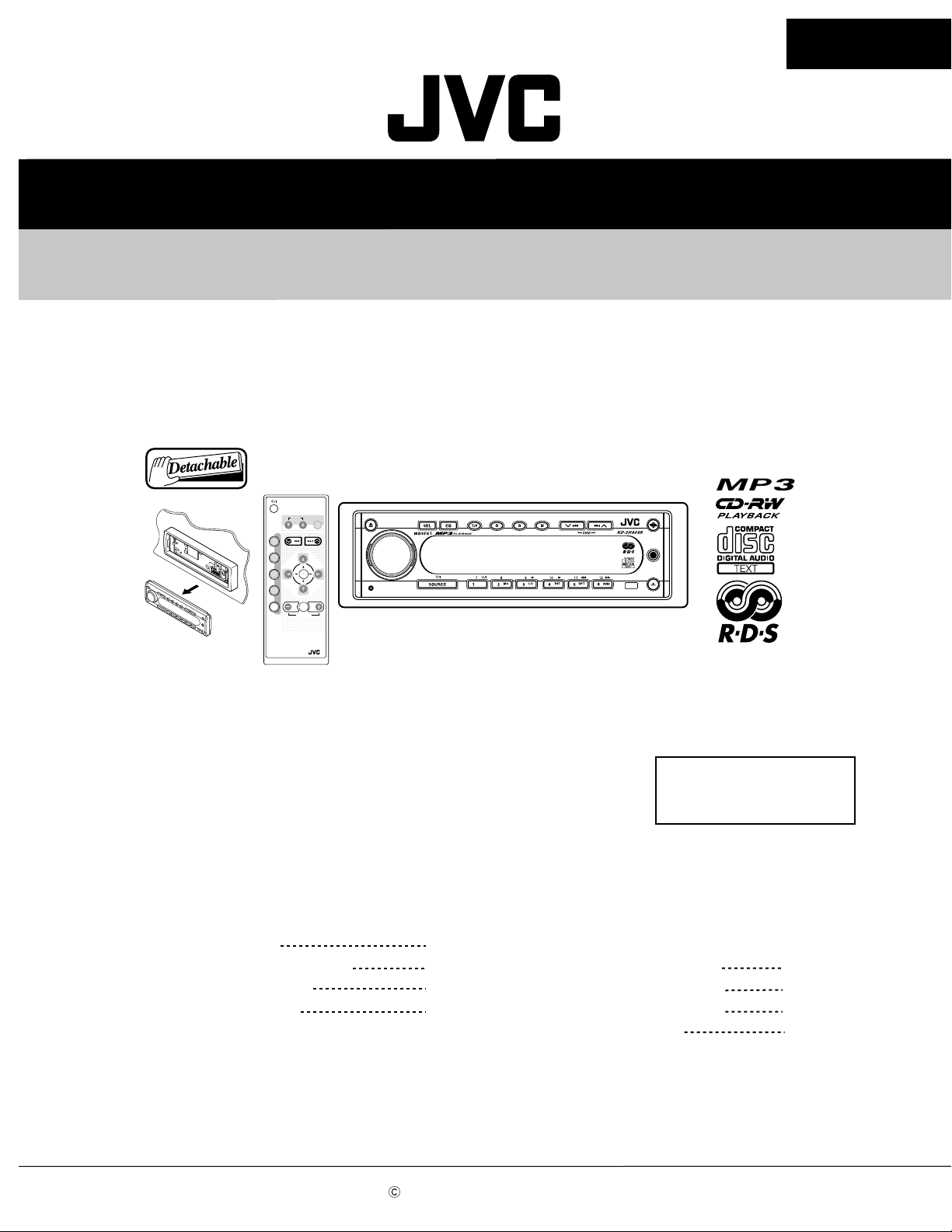
CD RECEIVER
KD-SH909R
KD-SH909R
Contents
Safety precaution
Preventing static electricity
Disassembly method
Adjustment method
ATT
ANGLE
CD
DAB
FM
PRESET
AM
CH
AUX SEL
RM-RK100
EQ
DISC
PRESET
R D
DISC
VOLUME
ATT
Area Suffix
E --------- Continental Europe
EX ------------- Central Europe
1-2
1-3
1-4
1-23
Flow of functional
operation unit TOC read
Maintenance of laser pickup
Replacement of laser pickup
Description of major ICs
1-24
1-26
1-26
1-27~51
COPYRIGHT 2002 VICTOR COMPANY OF JAPAN, LTD.
No.49712
Apr. 2002
Page 2
KD-SH909R
Safety precaution
!
!
Burrs formed during molding may be left over on some parts of the chassis. Therefore,
pay attention to such burrs in the case of preforming repair of this system.
Please use enough caution not to see the beam directly or touch it in case of an
adjustment or operation check.
1-2
Page 3
KD-SH909R
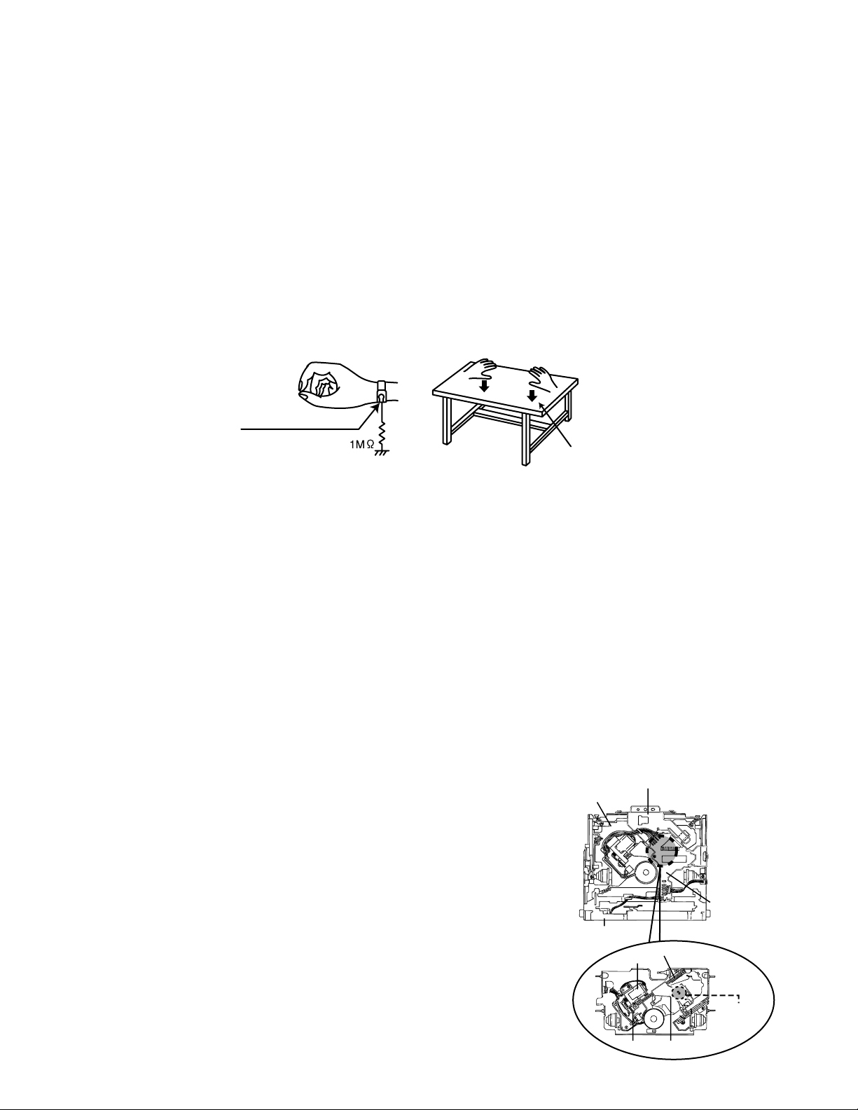
Preventing static electricity
1.Grounding to prevent damage by static electricity
Electrostatic discharge (ESD), which occurs when static electricity stored in the body, fabric, etc. is discharged,
can destroy the laser diode in the traverse unit (optical pickup). Take care to prevent this when performing repairs.
2.About the earth processing for the destruction prevention by static electricity
Static electricity in the work area can destroy the optical pickup (laser diode) in devices such as CD players.
Be careful to use proper grounding in the area where repairs are being performed.
2-1 Ground the workbench
Ground the workbench by laying conductive material (such as a conductive sheet) or an iron plate over
it before placing the traverse unit (optical pickup) on it.
2-2 Ground yourself
Use an anti-static wrist strap to release any static electricity built up in your body.
(caption)
Anti-static wrist strap
Conductive material
(conductive sheet) or iron plate
3. Handling the optical pickup
1. In order to maintain quality during transport and before installation, both sides of the laser diode on the
replacement optical pickup are shorted. After replacement, return the shorted parts to their original condition.
(Refer to the text.)
2. Do not use a tester to check the condition of the laser diode in the optical pickup. The tester's internal power
source can easily destroy the laser diode.
4.Handling the traverse unit (optical pickup)
1. Do not subject the traverse unit (optical pickup) to strong shocks, as it is a sensitive, complex unit.
2. Cut off the shorted part of the flexible cable using nippers, etc. after replacing the optical pickup. For specific
details, refer to the replacement procedure in the text. Remove the anti-static pin when replacing the traverse
unit. Be careful not to take too long a time when attaching it to the connector.
3. Handle the flexible cable carefully as it may break when subjected to strong force.
4. It is not possible to adjust the semi-fixed resistor that adjusts the laser power. Do not turn it
CD mechanism ass’y
Damper bracket
Attention when traverse unit is decomposed
*Please refer to "Disassembly method" in the text for pick-up and how to
detach the substrate.
1.Solder is put up before the card wire is removed from connector on
the CD substrate as shown in Figure.
(When the wire is removed without putting up solder, the CD pick-up
assembly might destroy.)
2.Please remove solder after connecting the card wire with
when you install picking up in the substrate.
Front bracket
Feed motor ass’y
FD screw
CD mechanism
control board
Soldering
FD gear
Pickup unit
1-3
Page 4
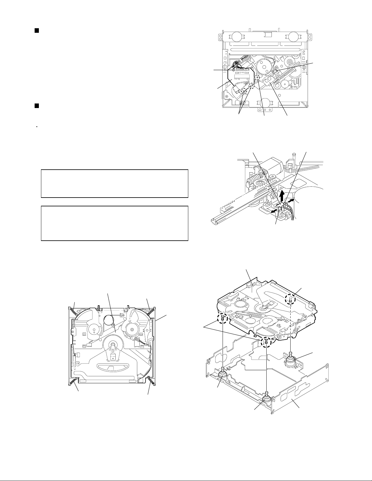
KD-SH909R
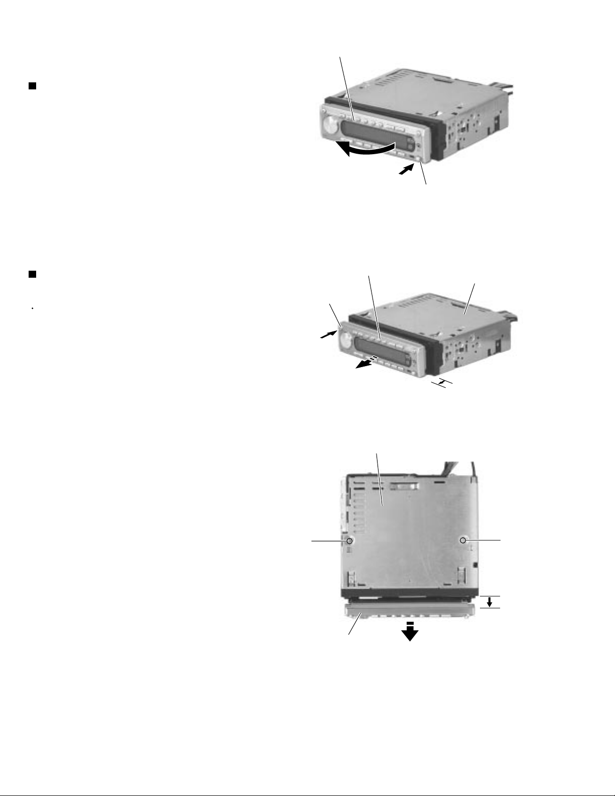
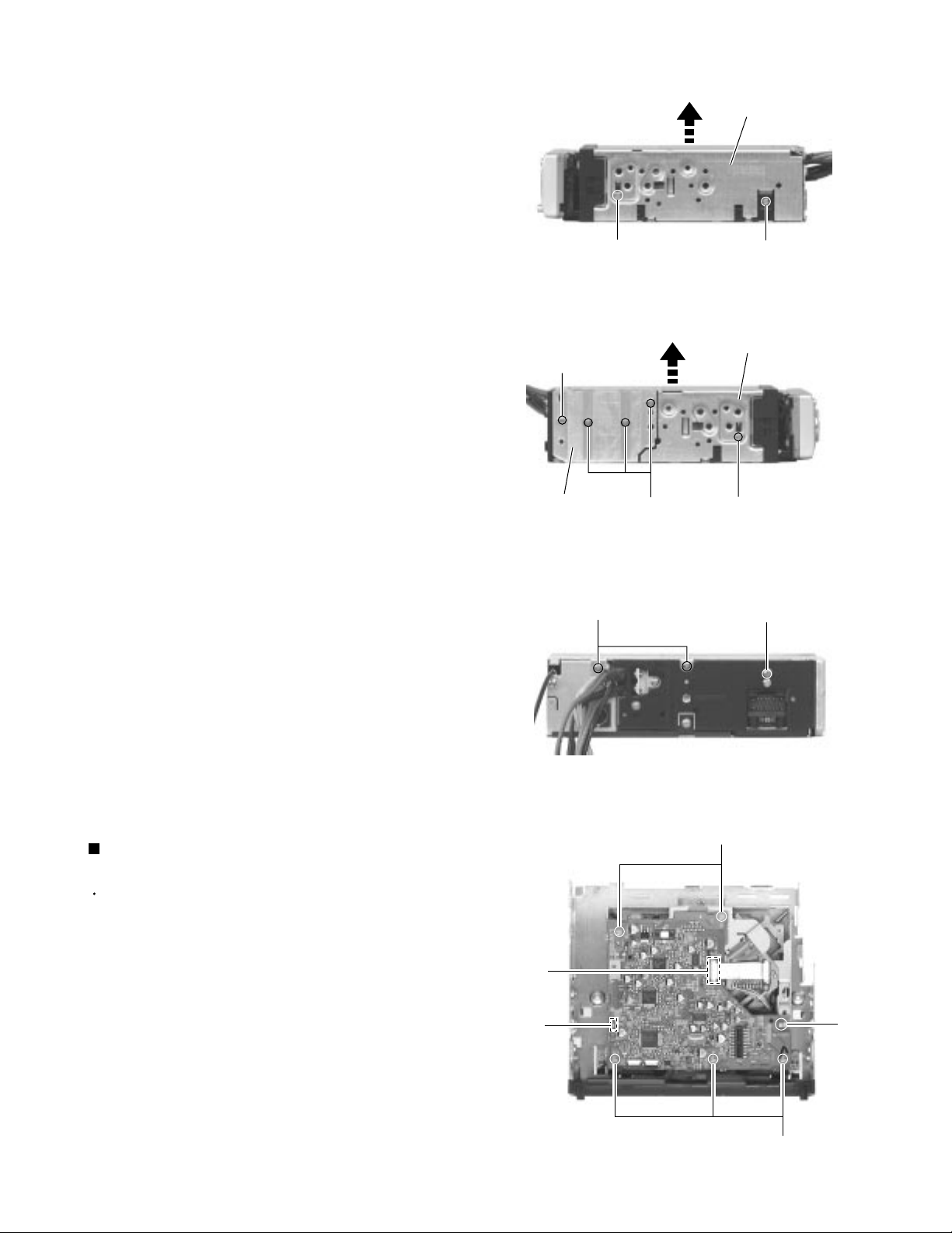
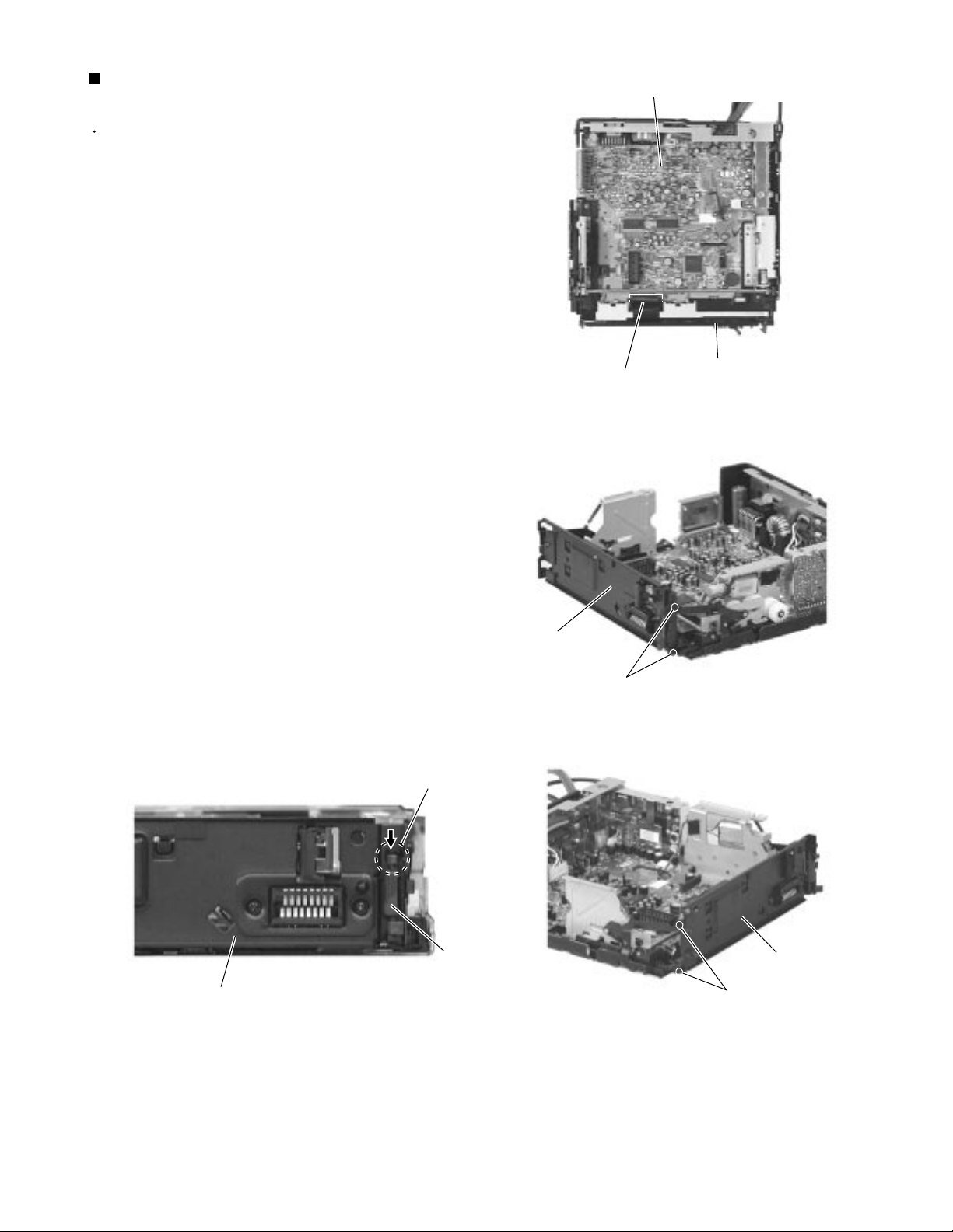
Disassembly method
Removing the front panel assembly
(See Fig.1)
1.
Press the release button in the lower right part of the
front panel assembly to unlock.
2.
Remove the front panel assembly in the direction of
the arrow.
Removing the top chassis
(See Fig.2 to 6)
Turn on power.
1.
Press the eject button in the upper left part of the
front panel assembly to move the assembly as
shown in Fig.2 and turn off power.
Front panel assembly
Front panel assembly
Eject button
Release button
Fig.1
Top chassis
2.
Remove the two screws A on the upper side of the
body.
Top chassis
A
Front panel assembly
Fig.2
A
Fig.3
1-4
Page 5
3.
Remove the three screws B on both sides of the
body.
4.
Remove the screw C and the three screws D on the
left side of the body.
5.
Remove the two screws E and the screw F on the
back of the body.
6.
Move the top chassis upward and remove it with the
CD mechanism assembly. The connector on the CD
mechanism assembly is disconnected from
connector CN601 on the main board.
KD-SH909R
Top chassis
BB
Fig.4
Top chassis
C
Removing the (A) board
(See Fig.7)
Prior to performing the following procedure, remove
the top cover.
Heat sink
E
BD
Fig.5
F
Fig.6
G
1.
Disconnect the wire from connector CN601on the (A)
board.
2.
Remove the five screws G and the (A) board, releasing
the joint a and b.
CN601
a
b
G
Fig.7
1-5
Page 6
KD-SH909R
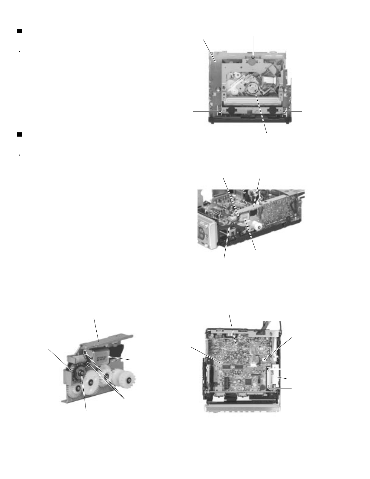
Removing the CD mechanism assembly
(See Fig.8)
Prior to performing the following procedure, remove
the top chassis.
1.
Remove the three screws H inside the top chassis
and remove the CD mechanisma ssembly.
Removing the motor assembly
(See Fig.9 to 11)
Prior to performing the following procedure, remove
the top chassis.
1.
Disconnect the wire from connector CN703 on the
main board.
2.
Remove the motor bracket and the spring attached
to the arm braket assembly (R).
Top chassis
H
Spring
H
H
CD mechanisma ssembly
Fig.8
Motor braket
3.
Remove the two screws I attaching the motor
bracket.
4.
Remove the washer attaching the clutch assembly
and pull out the clutch assembly from the shaft.
5.
Remove the two screws J and the motor assembly
from the motor bracket.
Motor braket
Clutch assembly
Motor assembly
Motor assembly
Arm braket assembly (R)
Fig.9
Main board
CN703
CN601
I
Motor braket
I
1-6
Washer
Fig.11
J
Fig.10
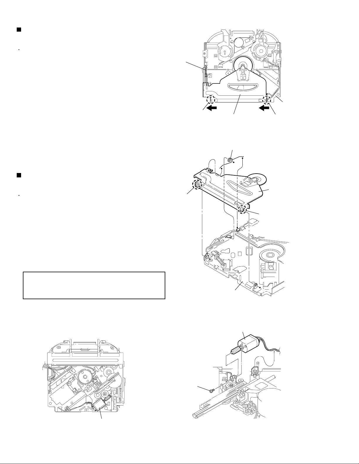
Page 7
Removing the main board
(See Fig.12 to 16)
Prior to performing the following procedures, remove
the top chassis and the motor bracket.
1.
Disconnect the flexible wire from connector CN701
and CN702 on the main board respectively.
2.
Move the front bracket backward until it stops.
3.
Remove the four screws K attaching the arm
brackets (L) and (R). Move the right and arm lefter
brackets from the rod gear.
4.
Remove the rod gear.
5.
Remove the screw M attaching the rear panel to the
bottom cover on the back of the body.
K
Arm
brackets (L)
K
CN701
L
CN702
Main board
Fig.12
KD-SH909R
L
Arm
brackets (R)
K
Rod gear
Arm brackets (R)
Arm brackets (L)
Main board
Rod gear
Fig.13
Rear panel
M
Fig.14
Bottom cover
1-7
Page 8
KD-SH909R
6.
Remove the two screws L and move the main board
backwards to release the two joints c. (The main
board will be removed with the rear panel and the
rear heat sink)
Joint c
7.
Remove the screw N and Q attaching the rear heat
sink.
8.
Remove the three screws O and the screw P
attaching the rear panel. Remove the main board.
Joint c
O
Rear panel
P
Q
Main board
Fig.15
N
Rear heat sink
Removing the lifter switch board
(See Fig.17)
Prior to performing the following procedures, remove
the top chassis, the motor bracket and the main
board.
1.
Remove the two screws R attaching the lifter switch
board.
Fig.16
Bottom cover
Lifter switch board
R
1-8
Fig.17
Page 9
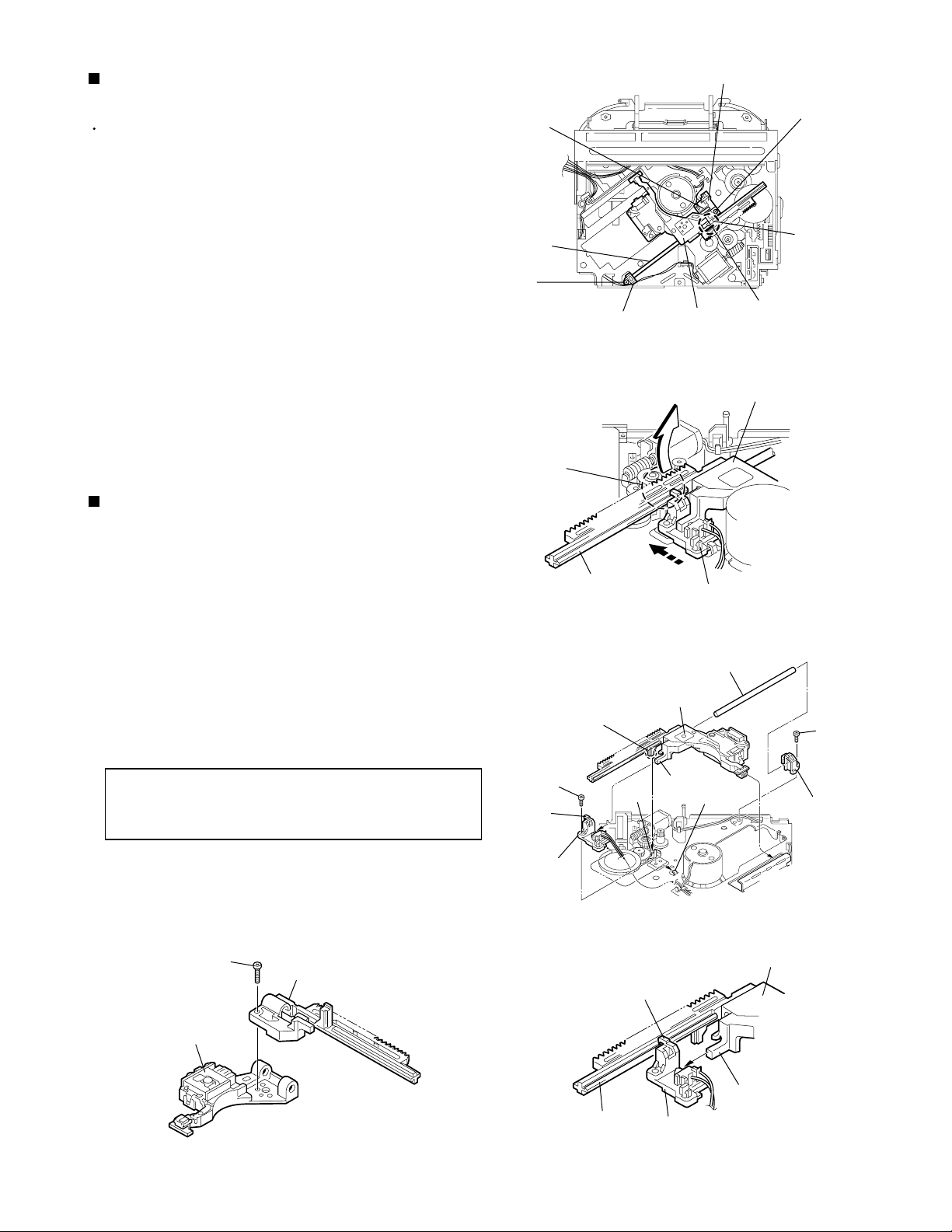
KD-SH909R
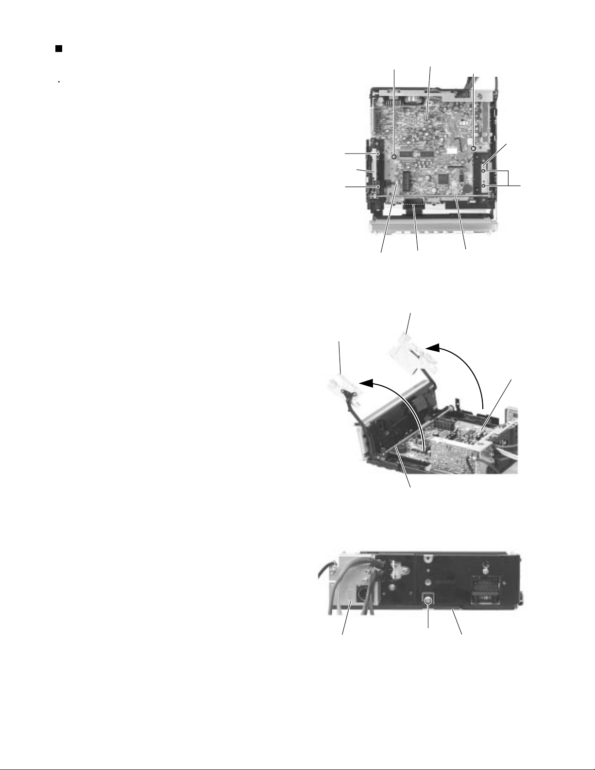
Removing the lifter board
(See Fig.18 to 24)
Prior to performing the following procedure, remove
the top chassis assembly and thefront panel
assembly.
1.
Disconnect the flexible wire from connector CN702
on the main board.
2.
Remove the four screws S attaching the front
bracket on both sides of the body.
3.
Push the pin of the joint d on the front of the front
bracket to release the lock lever.
Main board
CN702
Front bracket
Fig.18
Front bracket
Joint d
Lock lever
Front bracket
S
Fig.19
Front bracket
S
Fig.20Fig.21
1-9
Page 10
KD-SH909R
4.
Remove the screw T attaching the lifter board cover
in the rear of the front bracket.
5.
Release the two joints f while pushing the front side.
Move the lifter board cover inthe direction of the
arrow and release the eight joints e.
Joint f
Joints e
Lifter board cover
Joints e
Joint f
6.
Remove the two screws U attaching the lifter board
on the front of the body.
T
Joints e
Lifter board
Joint e
Front bracket
Fig.22
Lifter board cover
Fig.23
1-10
Fig.24
U
Page 11
KD-SH909R
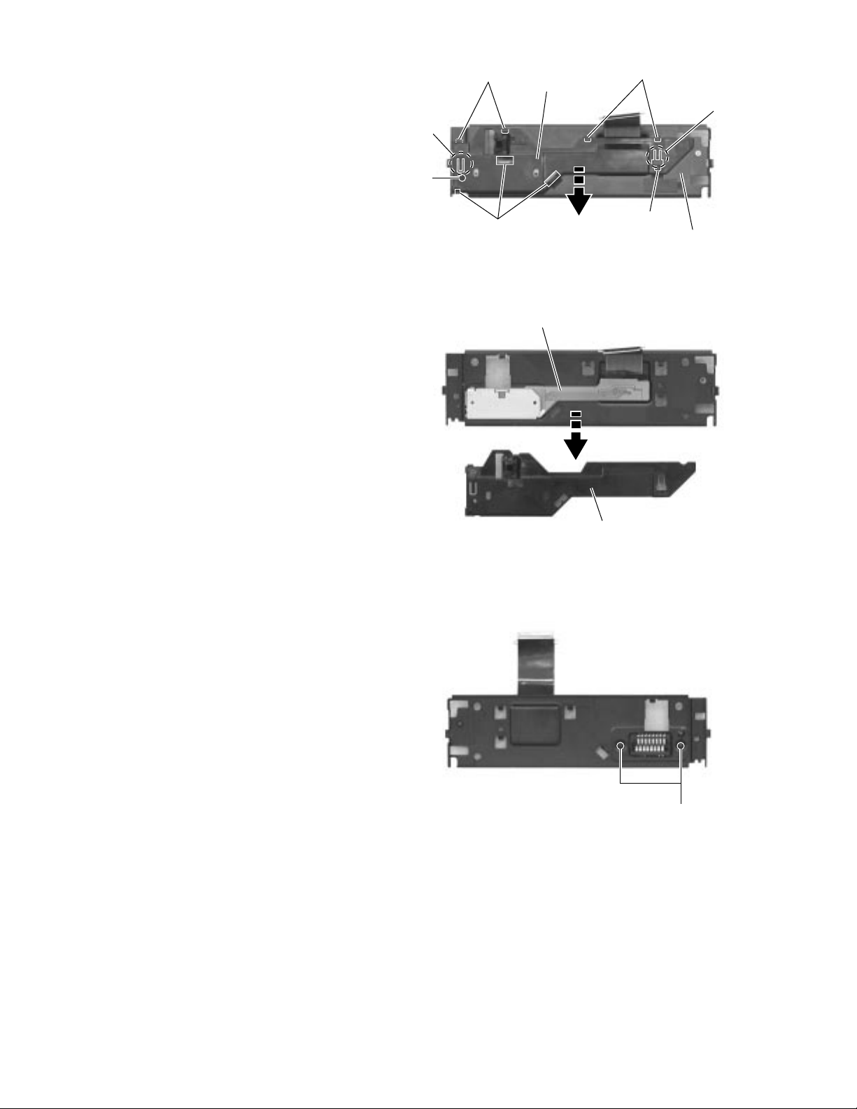
<Front panel assembly>
Prior to performing the following procedure, remove
the front panel assembly.
Removing the front board
(See Fig.25 and 26)
1.
Remove the four screws V attaching the rear panel
to the front panel assembly.
2.
Release the eleven joints g of the front panel and the
rear panel.
3.
Disconnect the wire from connector CN803 on the
front board.
4.
If necessary, unsolder the front board.
Removing the volume board
(See Fig.26 and 27)
V
W
Line in board
V
Joint g 11
Front board
Rear panel
Fig.25
Soldering
CN803
Soldering
W
W
V
V
Volume board
W
Prior to performing the following procedure, remove
the rear panel.
1.
Remove the four screws W attaching the volume
board.
2.
Disconnect the volume knob, ring lens and volume
ring from the volume board.
3.
If necessary, unsolder the volume board.
Removing the line in board
(See Fig.26 and 28)
Prior to performing the following procedure, remove
the rear panel.
1.
Disconnect the wire from connector CN803 on the
front board.
2.
Pull out the line in board from the front panel
assembly.
Fig.26
Volume board
Volume lens, Volume ring
Rng knob
Fig.27
Line in board
Fig.28
1-11
Page 12
KD-SH909R
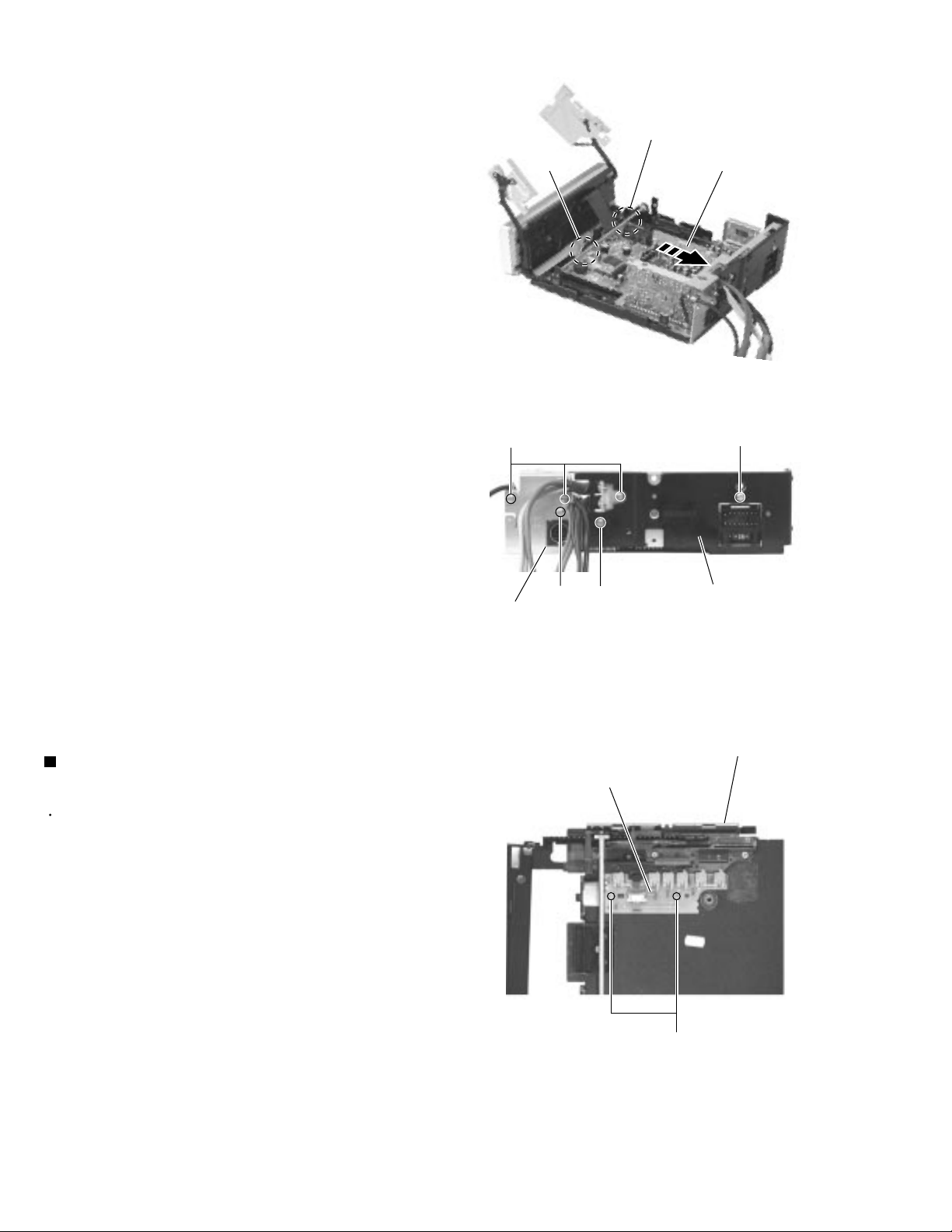
< CD mechanism section >
Removing the top cover
(See Fig.1 and 2)
1.
Remove the two screws A on each side of the body.
2.
Lift the front side of the top cover and move the
cover backward to release the two joints a.
Removing the connector board
(See Fig.3 to 5)
Top cover
A
A
Joints a
CAUTION:
1.
Remove the screw B fixing the connector board.
2.
Solder the short-circuit point on the connector board.
Disconnect the flexible wire from the pickup.
3.
Move the connector board in the direction of the
arrow to release the two joints b.
4.
Unsolder the wire on the connector board if
necessary.
CAUTION:
Before disconnecting the flexible wire
from the pickup, solder the short-circuit
point on the pickup. No observance of
this instruction may cause damage of
the pickup.
Unsolder the short-circuit point after
reassembling.
A
Fig.1
Joints a
Top cover
Fig.2
DET switch
B
1-12
Flexible wire
Frame
Connector board
B
Connector board
Joints b
Flexible wire
Short-circuit
Fig.3
Fig.4Fig.5
Pickup
Short-circuit point
(Soldering)
Pickup
Page 13
Removing the DET switch
(See Fig.3 and 6)
1.
Extend the two tabs c of the feed sw. holder and pull
out the switch.
2.
Unsolder the DET switch wire if necessary.
Removing the chassis unit
(See Fig.7 and 8)
Prior to performing the following procedure, remove
the top cover and the connector board.
B
Connector board
Joints b
Short-circuit
Fig.3
KD-SH909R
DET switch
Pickup
1.
Remove the two suspension springs (L) and (R)
attaching the chassis unit to the frame.
CAUTION:
The shape of the suspension spring (L)
and (R) are different. Handle them with
care.
CAUTION:
When reassembling, make sure that the
three shafts on the underside of the
chassis unit are inserted to the dampers
certainly.
Chassis unit
Suspension spring (R)
Suspension spring (L)
Frame
DET switch
Chassis unit
Tab c
Feed sw. holder
Tab c
Fig.6
Shaft
Suspension spring (R)
Suspension spring (L)
Shafts
Damper
Damper
Damper
Frame
Fig.8Fig.7
1-13
Page 14
KD-SH909R
Removing the clamper assembly
(See Fig.9 and 10)
Prior to performing the following procedure, remove
the top cover.
1.
Remove the clamper arm spring.
2.
Move the clamper assembly in the direction of the
arrow to release the two joints d.
Removing the loading / feed motor
assembly (See Fig.11 and 12)
Prior to performing the following procedure, remove
the top cover, the connector board and the chassis
unit.
1.
Remove the screw C and move the loading / feed
motor assembly in the direction of the arrow to
remove it from the chassis rivet assembly.
Clamper arm
spring
Joint d
Joint d
Clamper assembly
Fig.9
Clamper arm spring
Chassis rivet
assembly
Joint d
Clamper assembly
Joint d
2.
Disconnect the wire from the loading / feed motor
assembly if necessary.
CAUTION:
When reassembling, connect the wire
from the loading / feed motor assembly
to the flame as shown in Fig.11.
Chassis rivet assembly
Fig.10
Loading / feed motor assembly
C
1-14
Loading / feed motor assembly
Fig.12Fig.11
Page 15
KD-SH909R
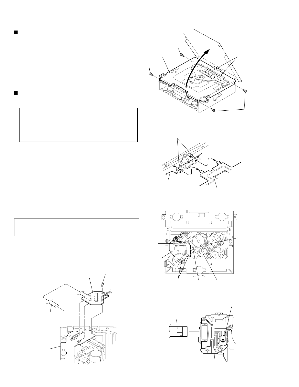
Removing the pickup unit
(See Fig.13 to 17)
Prior to performing the following procedure, remove
the top cover, the connector board and the chassis
unit.
1.
Remove the screw D and pull out the pu. shaft
holder from the shaft.
2.
Remove the screw E attaching the feed sw. holder.
3.
Move the part e of the pickup unit upward with the
shaft and the feed sw. holder, then release the joint f
of the feed sw. holder in the direction of the arrow.
The joint g of the pickup unit and the feed rack is
released, and the feed sw. holder comes off.
4.
Remove the shaft from the pickup unit.
5.
Remove the screw F attaching the feed rack to the
pickup unit.
Reattaching the pickup unit
(See Fig.13 to 16)
Joint f
Shaft
D
Joint e
Pu. shaft holder
Feed sw. holder
Pickup unit
Fig.13
Pickup unit
E
Joint f
Joint e
1.
Reattach the feed rack to the pickup unit using the
screw F.
2.
Reattach the feed sw. holder to the feed rack while
setting the joint tab g to the slot of the feed rack and
setting the part f of the feed rack to the switch of the
feed sw. holder correctly.
3.
As the feed sw. holder is temporarily attached to the
pickup unit, set to the gear of the joint g and to the
bending part of the chassis (joint h) at a time.
CAUTION:
4.
Reattach the feed sw. holder using the screw E.
5.
Reattach the shaft to the pickup unit. Reattach the
pu. shaft holder to the shaft using the screw D.
Make sure that the part i on the underside
of the feed rack is certainly inserted to the
slot j of the change lock lever.
F
Feed rack
E
Joint g
Feed sw. holder
Feed rack
Part i
Pickup unit
Slot j
Joint g
Feed sw. holder
Fig.14
Shaft
Joint f
Joint h
Fig.15
D
Pu. shaft holder
Pickup unit
Pickup unit
Feed rack
Joint f
Feed sw. holder
Fig.17Fig.16
1-15
Page 16
KD-SH909R
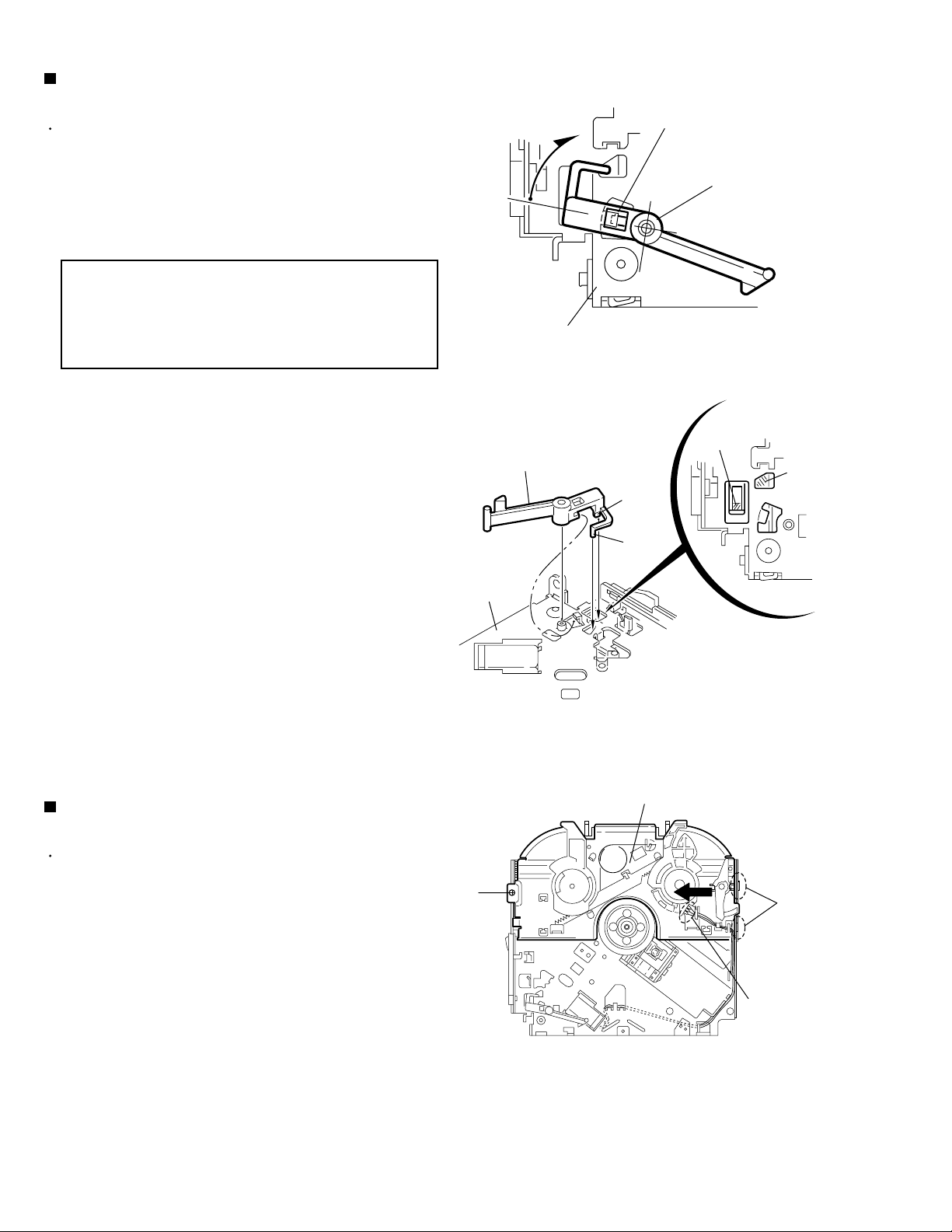
Removing the trigger arm
(See Fig.18 and 19)
Prior to performing the following procedure, remove
the top cover, the connector board and the clamper
unit.
1.
Turn the trigger arm in the direction of the arrow to
release the joint k and pull out upward.
Joint k
Trigger arm
CAUTION:
When reassembling, insert the part l and
m of the trigger arm into the part n and
o at the slot of the chassis rivet
assembly respectively and join the joint
k at a time.
Chassis rivet assembly
Chassis rivet assembly
Trigger arm
Fig.18
Part n
Part o
Part l
Part m
Fig.19
Removing the top plate assembly
(See Fig.20)
Prior to performing the following procedure, remove
the top cover, the connector board, the chassis unit,
and the clamper assembly.
1.
Remove the screw H.
2.
Move the top plate assembly in the direction of the
arrow to release the two joints p.
3.
Unsolder the wire marked q if necessary.
1-16
H
Top plate assembly
Joints p
q
Fig.20
Page 17

KD-SH909R
Removing the select arm (L) / select lock
arm (See Fig.21 and 22)
Prior to performing the following procedure, remove
the top plate assembly.
1.
Bring up the select arm (L) to release from the link
plate (joint r) and turn in the direction of the arrow to
release the joint s.
2.
Unsolder the wire of the select arm (L) marked q if
necessary.
3.
Turn the select lock arm in the direction of the arrow
to release the two joints t.
The select lock arm spring comes off the select lock
arm at the same time.
Reassembling the select arm (L) / select
lock arm (See Fig.23 to 25)
Select arm (R)
Joint z
Link plate spring
Top plate
Joint a'
Joint y
Link plate
Joint z
Joint s
Fig.21
Select lock arm
Select lock arm
Joint b'
Joint r
Select arm (L)
Select lock arm
q
Top plate
Hook u
Select lock
arm spring
Joints t
REFERENCE:
1.
Reattach the select lock arm spring to the top plate
Reverse the above removing procedure.
and set the shorter end of the select lock arm spring
to the hook u on the top plate.
2.
Set the other longer end of the select lock arm spring
to the boss v on the underside of the select lock arm,
and join the select lock arm to the slots (joint t). Turn
the select lock arm as shown in the figure.
3.
Reattach the select arm (L) while setting the part r to
the first peak of the link plate gear, and join the joint
s.
CAUTION:
When reattaching the select arm (L),
check if the points w and x are correctly
fitted and if each part operates properly.
Joint r
Link plate
Link plate
Select lock arm spring
Boss v
Select arm (R)
Joint a'
Fig.22
Hook u
Joint t
Joint t
Select lock arm
Fig.23
Link plate spring
Select arm (L)
Joint b'
Joint r
Fig.25Fig.24
Joint s
Select
lock arm
Point x
1-17
Page 18

KD-SH909R
Removing the select arm (R) / link plate
(See Fig.21 and 22)
Prior to performing the following procedure, remove
the top plate assembly.
1.
Bring up the select arm (R) to release from the link
plate (joint y) and turn as shown in the figure to
release the two joints z and joint a’.
2.
Move the link plate in the direction of the arrow to
release the joint b’. Remove the link plate spring at
the same time.
REFERENCE:
Before removing the link plate, remove
the select arm (L).
Reattaching the Select arm (R) / link
plate (See Fig.25 and 26)
REFERENCE:
Reverse the above removing procedure.
Select arm (R)
Joint z
Link plate spring
Top plate
Joint a'
Part y
Link plate
Joint z
Joint s
Fig.21
Select lock arm
Select lock arm
Joint b'
Joint r
Select arm (L)
Select lock arm
q
Top plate
Hook u
Select lock
arm spring
1.
Reattach the link plate spring.
2.
Reattach the link plate to the link plate spring while
joining them at joint b’.
3.
Reattach the part y of the select arm (R) to the first
peak of the link plate while joining the two joints z
with the slots. Then turn the select arm (R) as shown
in the figure. The top plate is joined to the joint a’.
CAUTION:
When reattaching the select arm (R),
check if the part c’ is correctly fitted and
if each part operates properly.
Select arm (R)
Joint z
Link plate
Link plate spring
Joint a'
Part y
Part y
Fig.22
Joint b'
Joint z
Fig.25
Joints t
Select arm (L)
Select
lock arm
Point x
1-18
Link plate
Fig.26
Page 19

KD-SH909R
Removing the loading roller assembly
(See Fig.27 to 29)
Prior to performing the following procedure, remove
the clamper assembly and the top plate assembly.
1.
Push inward the loading roller assembly on the gear
side and detach it upward from the slot of the joint d’
of the lock arm rivet assembly.
Detach the loading roller assembly from the slot of
the joint e’ of the lock arm rivet assembly.
The roller guide comes off the gear section of the
loading roller assembly.
Remove the roller guide and the washer from the
shaft of the loading roller assembly.
2.
Remove the screw I attaching the lock arm rivet
assembly.
3.
Push the shaft at the joint f’ of the lock arm rivet
assembly inward to release the lock arm rivet
assembly from the slot of the slide plate. Extend the
lock arm rivet assembly outward and release the
joint g’ from the boss of the chassis rivet assembly.
The roller guide springs on both sides come off.
Roller guide
Washer
Loading roller assembly
Roller guide
Joint e'
Roller guide spring
Roller guide spring
Joint d'
Loading roller assembly
Roller guide spring
Lock arm rivet assembly
Fig.27
Loading roller assembly
Roller guide
spring
CAUTION:
When reassembling, reattach the left
and right roller guide springs to the lock
arm rivet assembly before reattaching
the lock arm rivet assembly to the
chassis rivet assembly. Make sure to fit
the part h’ of the roller guide spring (L)
inside of the roller guide (Refer to
Fig.30).
Roller guide
Washer
Roller shaft assembly
Joint h'
Loading roller assembly
Roller guide
spring
Fig.28-1
Fig.28-2
Chassis rivet assembly
Boss
Slide plate
Roller guide spring
I
Frame
Loading roller
Roller guide spring
Lock arm rivet assembly
Joint f'
Part g'
Fig.29Fig.30
1-19
Page 20

KD-SH909R
Removing the loading gear (5), (6) and
(7) (See Fig.31 and 32)
Prior to performing the following procedure, remove
the top cover, the chassis unit and the top plate
assembly.
1.
Remove the screw J attaching the loading gear
bracket. The loading gear (6) and (7) come off the
loading gear bracket.
2.
Pull out the loading gear (5).
Loading gear bracket
J
Loading gear (6)
Loading gear (5)
Loading gear (3)
Fig.31
J
Loading gear bracket
Loading gear (5)
Loading gear (6)
Loading gear (7)
Fig.32
1-20
Page 21

Removing the gears (See Fig.33 to 36)
Prior to performing the following procedure, remove
the top cover, the chassis unit, the top plate
assembly and the pickup unit.
1.
Pull out the feed gear.
KD-SH909R
Slot j'
Slide plate
2.
Move the loading plate assembly in the direction of
the arrow to release the slide plate from the two slots
j’ of the chassis rivet assembly.
3.
Detach the loading plate assembly upward from the
chassis rivet assembly while releasing the joint k’.
Remove the slide hook and the loading plate spring
from the loading plate assembly.
4.
Pull out the loading gear (2) and remove the change
lock lever.
5.
Remove the E-washer and the washer attaching the
changer gear (2).
6.
The changer gear (2), the changer gear spring and
the adjusting washer come off.
7.
Remove the loading gear (1).
8.
Move the hang plate rivet assembly in the direction
of the arrow to release from the three shafts of the
chassis rivet assembly upward.
9.
Detach the loading gear plate rivet assembly from
the shaft of the chassis rivet assembly upward while
releasing the joint l’.
Feed gear
Change plate
rivet assembly
Shafts
E-washer
Loading plate assembly
Joint k'
Slot j'
Fig.33
Joint l'
Loading gear (4)
Loading gear plate
rivet assembly
Loading gear (2)
Loading gear (1)
Change gear (2)
10.
Pull out the loading gear (4).
Loading plate assembly
Loading plate spring
Slot j'
Chassis rivet assembly
Joint k'
Slide hook
Slide plate
Slot j'
E-washer
Washer
Loading gear (2)
Loading plate spring
Adjusting washer
Change plate
rivet assembly
Chassis rivet assembly
Fig.34
Loading gear (1)
Loading gear (2)
Change lock lever
Loading gear (4)
Loading gear plate rivet assembly
Fig.36Fig.35
1-21
Page 22

KD-SH909R
Removing the turn table / spindle motor
(See Fig.37 and 38)
Prior to performing the following procedure, remove
the top cover, the connector assembly and the
chassis / clamper assembly.
1.
Remove the two screws K attaching the spindle
motor assembly through the slot of the turn table on
top of the body.
2.
Unsolder the wire on the connector board if
necessary.
K
Turn table
Fig.37
K
Turn table
1-22
Spindle motor
Fig.38
Page 23

Adjustment method
KD-SH909R
Test instruments required adjustment
1.Digital oscilloscope (100MHz)
2.AM Standard signal generator
3.FM Standard signal generator
4.Stereo modulator
5.Electric voltmeter
6.Digital tester
7.Test disc(CTS-1000)
8.Extension cable for check
EXTGS004-22P
Standard measuring conditions
Power supply voltage DC 14.4V(11V to 16V allowance)
Load impedance 4 (4 to 8 allowance)
Line-out Level/Impedance
: 2.0 V/20k load(full scale)
Output impedance : 1k
Standard volume position
Balance and Bass & Treble volume : Indication "0"
Loudness : OFF
Frequency Band
FM 87.5kHz - 108.0 kHz
(MW) 522kHz - 16200kHz
AM
(LW) 144kHZ - 279kHz
Dummy load
Exclusive dummy load should be used for AM, and FM.
For FM dummy load, there is a loss of 6dB between SSG output
and antenna input. The loss of 6dB need not be considered
since direct reading of figures are applied in this workingo
standard.
How to connect the extension cable for adjusting
Extension cables
EXTGS004-26P
CN701
CD Mechanism
Front panel ass'y
1-23
Page 24

KD-SH909R
Flow of functional operation unit TOC read
Power ON
When the pickup correctly moves
v
to the inner area of the disc
Set Function CD
When the laser diode correctly
emits
Microprocessor
commands
FMO
TC94A14FA" 40"
FEED MOTOR
+TERMINAL
IC561"4"
REST SW
When correctly focused
FEO
TA2157" 15"
Focus Servo Loop ONo
$83
$82
$81
3.3V
Hi-Z
0V
6V
4V
2V
OFF
ON
Pickup feed to the inner area
2.2V
RF signal eye-patternn
remains closed
RF signal eye-pattern
opens
Disc inserted
YES
Laser emitted
Focus search
Disc rotates
Tracking loop closed
TOC read out
YES
Microprocessor
commands
SEL
TC94A14FA"38"
LD
CN501"15"
"No disc"
display
When the disc correctly rotates
Microprocessor
commands
DMO
TC94A14FA"41"
Spindle
motor(-)
IC561"1"
$84 $86 $ A200
Acceleration Servo CLV
Rough
Servo
0.5 Sec 0.5 Sec
$84
3.3V
0V
4V
0V
3.3V
2.2V
0V
6V
3.2
2V
1-24
Jump to the first track
Play
Tracking Servo Loop ON
RF signal
Rough Servo Modev
CLV Servo Mode
(Program Area)
CLV Servo Mode
(Lead-In Area;
Digital :0)
Page 25

Feed section
Is the voltage output at
IC521 pin "40" 5V or 0V?
YES
Is 4V present at both
sides of the feed motor?
YES
NO YES NO
NO
Is the wiring for IC521
(56)~(64) correct?
NO
Is 6V or 2V present at
IC561 "4" and "5"?
NO
Is 3.3V present at IC561
pin "20"?
Check the vicinity of
IC521.
YES
Check the feed motor
connection wiring.
YES
Check CD 8V
KD-SH909R
and 5V.
Check the feed motor.
Focus section
When the lens is
moving:
4V
Does the S-search
waveform appear at
IC561 pins "8" and "9"?
Spindle section
Is the disk rotated?
YES
Does the RF signal
appear at TP1?
YES
Is the RF waveform at TP1
distorted?
YES
Proceed to the Tracking
section
Check IC561.
NO
YES
NO
NO
NO
Check the circuits in
the vicinity of IC561
pins "8","9"and"15".
Check the pickup and
its connections
Is 4V present at IC561
pins "6" and "7"?
Check the spindle motor
and its wiring
Check the circuits in the
vicinity of IC501 "19"~
"24" or the pickup
YES
YES
NO
Is 4V present at IC521
pins "41" ?
Check the vicinity of
IC561.
NO
YES
Check IC521 and
IC501.
Tracking section
When the disc is rotated
at first:
Is the tracking error signal
output at IC501 "11"?
Check IC521.
Approx. 1.2V
YES
YES YES
Check the circuit in the
vicinity of IC501 pins
"2"~"12".
Check the pickup and
its connections
1-25
Page 26

KD-SH909R
Maintenance of laser pickup
(1) Cleaning the pickup lens
Before you replace the pickup,please try to
clean the lens with a alcohol soaked cotton
swab.
(2) Life of the laser diode
When the life of the laser diode has expired.
the following symptoms will appear..
(1) The level of RF output (EFM output:amplitude
of eye patterrn) will be low.
Is RF output
1.3 0.4Vp-p?
YES
O.K
(3) Semi-fixed resistor on the APC PC board
The semi-fixed resistor on the APC printed
circuit board which is attached to the pickup
is used to adjust the laser power.Since this.
adjustment should be performed to match the
characteristics of the whole optical block,
do not touch the semi-fixed resistor..
If the laser power is lower than the specified
value, the laser diode is almost worn out, and
the laser pickup should be replaced.
If the semi-fixed resistor is adjusted while
the pickup is functioning normally, the laser
pickup may be damaged due to excessive current.
NO
Replace it.
Replacement of laser pickup
Turn of the power switch and, disconnect the
power cord.
Replace the pickup with a normal one.(Refer
to "Pickup Removal" on the previous page)
Plug the power cord in, and turn the power on.
At this time, check that the laser emits for
about 3seconds and the objective lens moves
up and down.
Note: Do not observe the laser beam directly..
1-26
Play a disc.
Check the eye-pattern at TP1.
Finish.
Page 27

Description of major ICs
+
+
-
-
+
+
-
-
-
+
+
BA3220FV-X (IC301,IC401) : Line out amp
1.Pin layout
LGND
13
8
OUTL OUTR RGND
14
3220
17
2.Block diagram
CL-
14
KD-SH909R
CR-
1112
10
9
CR+
8
REFL
1
2
Vcc
3
INL
4
NFLCL+
REFR
FILTER
56
FIL
NFR
7
INR
1-27
Page 28

KD-SH909R
UPD784217AGC177 (IC701) : CPU
1. Pin layout
75 ~ 51
100 ~ 76
1 ~ 25
2. Pin function (1/2)
Pin No. FunctionSymbol I/O
1 5
6
7
8
9
10
11
12
13
14
15
16
17
18
19
20
21
22
23
24
25
26
27
28
29
30
31
32
33
34
35
36
37
38
39
40
41
42
43
44
45
NC
CD-MUTE
CD-REST
ANT REM
VDD
X2
X1
VSS
XT2
XT1
RESET
P.REQ
BUS-INT
PS2
NC
RDS-SCK
RDS-DA
REMOCON
AVDD
AVREF0
SD/ST
MRC DATA
KEY0
KEY1
TEMP
LEVEL
SQ
S.METER
AVSS
INLOCK
NC
AVREF
BUS-SI
BUS-SO
BUS-SCK
LCD-CE1
LCD-DA
LCD-CL
LCD-CE2
BUZZER
EPDAI
26 ~ 50
Non connect
CD MUTE
O
CD REST
O
Antenna remote output
O
5V connection
Connect to X'tal for main clock
Connect to X'tal for main clock
Connect to GND
Connect to X'tal for sub clock
Connect to X'tal for sub clock
Reset detection terminal
I
Mechanism power supply ON/OFF demand output ("L" on demand)
O
J-BUS signal interrupt input
I
Power save 2
I
Non connect
Clock input for RDS
I
RDS data input
I
Remocon signal input
I
5V connect
I
5V connect
I
Station detector, Stereo signal input
I
MRC data input
I
Key input 0
I
Key input 1
Temperature data input for contrast correction
I
Level meter input
S.quality level input
I
S.meter level input
I
Connect to GND
Lock detection output
I
Non connect
O
5V connect
I/O
J-BUS data input
I
J-BUS data output
O
J-BUS clock input/output
O
Chip enable 1 out put for LCD driver
O
Data output for LCD driver
O
Clock output to LCD driver
O
Chip enable 2 out put for LCD driver
O
Buzzer output
O
Communication data input 12C
I
1-28
Page 29

KD-SH909R
2. Pin function (2/2)
Pin No. FunctionSymbol I/O
46
47
48
49
50
51
52
53
54
55
56~61
62
63
64
65
66
67
68
69
70
71
72
73
74
75
76
77
78
79
80
81
82
83
84
85
86
87
88
89
90
91
92
93
94
95
96
97
98
99
100
EP-DAO
EPCLK
BUS-I/O
PM0
PM1
EQ-CLK
EQ-DA
EQ-LA
STAGE
VCR CONT
PNL-SW1~6
AFCK
SEEK/STOP
S.MUTE
FM/AM
PLL-CE
PLL-DO
PLL-CLK
PLL-DI
TEL MUTE
AMP KILL
VSS
DIMMER-IN
PS1
POWER
CD-ON
MUTE
W-LPF1
W-LPF2
W-MUTE
VDD
VOL-DA
VOL-CLK
CF SEL
PMKICK
SELECT
DIM-CONT
VOL-1
VOL-2
J/U
NC
NC
NC
TEST
NC
NC
NC
NC
DISCSEL
NC
Communication data input of 12C
O
Communication data input of 12C
O
J-BUS I/O switching output
O
Panel close side motor control signal output
O
Panel open side motor control signal output
O
Equalizer clock
O
Equalizer data
O
Equalizer latch
O
H:L: Initialization port
I
VCR control signal output
O
Panel position detection switch 1 to 6 signal input
I
AF clock output
O
SEEK:H STOP:L
O
Signal mute output
O
FM / AM select output
O
PLL IC control CE output
O
PLL IC control data output
O
PLL IC control clock output
O
PLL IC control data input
I
Telephone mute signal detection input
I
Amp off signal input
I
Connect to GND
Dimmer detection input
I
Power save 1
I
Power ON / OFF select output
O
Non connect
Mute output
O
Sub woofer cut off frequency control output 1
O
Sub woofer cut off frequency control output 2
O
Sub woofer mute output
O
5V connect
O
E. volume IC control data output
O
E. volume IC control clock data output
O
FM band area filter select signal output
O
Panel motor kick signal output
O
Non connect
Dimmer control signal output
O
Rotary volume pulse
I
Rotary volume pulse signal input
I
Pull down
I
Non connect
Non connect
Non connect
Connect to GND
I/O
Non connect
Non connect
Non connect
Non connect
H: 8 cm disc non correspondence L: 8 cm disc correspondence
O
Non connect
-
UPD784217AGC177
1-29
Page 30

KD-SH909R
UPD784225GK-623 (IC501) : CPU
1.Pin layout
60 ~ 41
61
40
~
80
1 ~ 20
2.Pin functions (1/2)
Pin No.
1
2,3
4
5
6
7
8
9
10
11
12
13
14
15
16
17
18
19
20
21
22
23
24
25
26
27
28
29
30
31
32
33
34
35
36
37
38
39
40
41~43
44
45
46
Symbol
TEMP IN
-
AVSS
ADCONT
-
AVREF1
EPROMDI
EPROMDO
EPROMCK
LCD CE
LCD DA
LCD CK
BUS I/O
BUS I/O
BUS SI
BUS SO
BUS SCK
BUSOUT
CD ON
CD REQ
CD MUTE
-
DSP RESET
CCE
BUCK
BUS3
BUS2
BUS1
BUS0
2X PLAY
RW SEL
VSS1
LD
LD/FE
MP3 DI
MP3 DO
MP3 CK
MP3 RESET
MP3 STB
-
DAC ML
DAC MC
DAC MD
21
~
I/O
I
-
-
O
-
I
O
I/O
O
O
O
O
O
I
O
I/O
O
O
O
O
O
O
O
I/O
I/O
I/O
I/O
O
O
O
O
I
O
O
O
O
O
O
O
Function
Temp. detection input terminal
No use
Connect to GND
Output H level at power to on
Connect to 3.3V
EEPROM data input terminal
EEPROM data output terminal
EEPROM clock signal input/output terminal
Chip enable output for LCD driver
Data output for LCD driver
Clock outout for LCD driver
JVC BUS input/output control terminal (negative)
JVC BUS input/output control terminal
JVC BUS data input terminal
JVC BUS data output terminal
JVC BUS clock input/output terminal
JVC BUS BUSOUT output terminal
Power supply (3.3V) control for CD
CD mechanism power supply to on request signal output terminal
CD mute signal output terminal
CD DSP reset signal output terminal
CD DSP chip enable output terminal
CD DSP data clock output terminal
CD DSP data 3 input/output terminal
CD DSP data 2 input/output terminal
CD DSP data 1 input/output terminal
CD DSP data 0 inout/output terminal
RF frequency responce select output of 2xspeed playback
CD-RW select output terminal (RW:L)
Connect to GND
Loading signal output terminal
Loading/Feed select signal output terminal (H:LD,L:FE)
CD MP3 data input terminal
CD MP3 data output terminal
Clock signal output terminal for CD MP3 data
CD MP3 reset signal output terminal
CD MP3 standby signal output terminal (H:Standby)
DAC mode control latch output terminal
DAC mode control BCK output terminal
DAC mode control data output terminal
1-30
Page 31

2.Pin functions (2/2)
KD-SH909R
Pin No.
47
48~51
52
53
54
55
56
57
58
59
60
61
62
63
64
65
66
67
68
69
70
71
72
73
74
75
76
77
78
79
80
Symbol
DAC CS
-
DISC SEL
DAC SEL
-
TEST MODE
MP3 SEL
8V DET
REST
SW2
RESET
SW1
B.DET
P. D E T
BUS INT
MP3 REQ
-
VSS0
VDD1
X2
X1
VPP
XT2
XT1
VDD0
AVDD
IOP
KEY0
KEY1
KEY2
KET3
I/O
O
I
I
I
I
I
I
I
I
I
I
I
I
I
-
-
-
O
I
-
O
I
-
I
I
I
I
I
Function
DAC chip select terminal
No use
8cm disc corespondance mode select terminal (respondance:L)
DAC select mode input terminal
LCD/AD key/Remocon invalid select mode input terminal L:invalid
MP3 select mode input terminal
CD mechanism power supply detection terminal (L:8V on)
CD mechanism rest switch input terminal
CD mechanism SW2 input terminal
Riset signal input terminal
CD mechanism SW1 input terminal
Backup power supply detection input terminal (H:Stop mode)
Main power off detection input terminal (H:HALT mode)
JVC BUS comunication start squeeze input terminal
CD MP3 request signal input terminal
Connect to GND
Connect to 3.3V
Ocsillator (6MHz)
Oscillator (6MHz)
Connec to GND
Open
Connect to GND
Connect to 3.3V
Connect to ADCONT
Pickup IOP measurment input terminal
Key input 0 (8bit A/D input) terminal
Key input 1 (8bit A/D input) terminal
Key input 2 (8bit A/D input) terminal
Key input 3 (8bit A/D input) terminal
1-31
Page 32

KD-SH909R
LA6579H-X (IC681) : 4-Channel bridge driver
1. Pin layout & Block diagram
VIN1-A
VIN1+A
VCCP1
1
+
VIN1_SW
[H]: OP-AMP_A
[L]: OP-AMP_B
2
3
[H]
[L]
28
VIN1
27
VIN1-B
-
+
26
VIN1+B
VO+
VO-
VO2+
VO2-
FR
VO3+
VO3-
VO4+
4
5
6
7
FR
8
9
10
Power system
GND
Level shift
33k
11k
-
Signal system
power supply
25
S-GND
+
24
VIN1-SW
Level shift
+
Level shift
Level shift
All outputs ON/OFF
H : ON
L : OFF
3.3VREG
(External:PTP Tr)
MUTE
Power system GND
Signal system
power supply
23
MUTE
22
VREFIN
FR
21
20
FR
VCCS
3.3VREG
+
-
19
REGIN
1-32
VO4-
VCCP2
VIN4
VIN4G
11
12
13
14
11k
33k
+
33k
33k
18
VIN2G
11k
-
17
VIN2
+
16
VIN3G
11k
-
15
VIN3
+
Page 33

3.Pin function
Pin No. Symbol Function
1
2
3
4
5
6
7
8
9
10
11
12
13
14
15
16
17
18
19
20
21
22
23
24
25
26
27
28
VIN1-A
VIN1+A
VCCP1
VO1+
VO1VO2+
VO2VO3+
VO3VO4+
VO4VCCP2
VIN4
VIN4G
VIN3
VIN3G
VIN2
VIN2G
REGIN
3.3VREG
VCCS
VREFIN
MUTE
VIN1_SW
S_GND
VIN1+B
VIN1-B
VIN1
CH1 input AMP_inverted input
CH1 input AMP_non-inverted input
CH1 and CH2 power stage power supply
Output pin(+)for channel 1
CH1 output pin (-) for channel 1
Output pin(+)for channel 2
Output pin(-)for channel 2
Output pin(+)for channel 3
Output pin(-)for channel 3
Output pin(+)for channel 4
Output pin(-)for channel 4
CH3 and CH4 power stage powr supply
Input pin for channel 4
Input pin for channel 4(for gain adjustment)
Input pin for channel 3
Input pin for channel 3(for gain adjustment)
Input pin for channel 2
Input pin for channel 2(for gain adjustment)
External PNP transistor, base connection
3.3VREG output pin, external PNP transistor,collector connection
Signal system GND
Reference voltage application pin
Output ON/OFF pin
CH1 input OP AMP_changeover pin
Signal system GND
CH1 AMP_B non-inverted input pin
CH1 AMP_B inverted input pin
CH1 input pin, input OP_AMP output pin
KD-SH909R
IC-PST9333U-X (IC702) : Regulator
1. Pin layout
NC 1
GND 2
3. Pin function
Pin No.
1
2
3
4
Symbol
GND
VOUT
4 Vcc
3 VOUT
Function
NC
Non connect
GND terminal
Reset signal output terminal
Vcc
Vcc terminal/Voltage detect terminal
Vcc 4
NC 1
2. Block diagram
3 VOUT
2 GND
1-33
Page 34

KD-SH909R
TA2157FN-X (IC601) : RF amp
1.Terminal layout
2.Block diagram
24 ~ 13
1 ~ 12
13
14
15
16
17
18
19
21
20
10pF
20k
20k
40k30k
20k 20k
15k
50 A
12k
12k
BOTTOM
PEAK
20k
20k
20k
PEAK
1.3V
40k
40k
240k
15pF
240k
15pF
50k
2k
20k
50k
14k
K
1
15k
x0.5
x2
x0.5
x2
1k
2k
1.75k
10pF
12
11
10
9
8
7
6
5
4
1-34
22
23
24
PIN SEL
VCTRLPIN
VCC
HiZ
GND
3k
3k
(APC SW)
APC ON
APC ON
APC OFF
(LDO=H)
180k
40pF
TEB
(TE BAL)
-50%
0%
+50%
180k
40pF
60k
60k
94k
22k
94k
22k
RFGC
(AGC Gian)
+12dB
+6dB
0dB
3
2
1
TEB
(TE BAL)
Normal mode
(0dB)
Normal mode
(0dB)
CD-RW mode
(+12dB)
Page 35

3.Pin function
Pin No. Symbol I/O Function
1
VCC
2
FNI
3
FPI
4
TPI
5
TNI
6
MDI
7
LDO
8
SEL
-
3.3V power supply pin
I
Main-beam amp input pin
I
Main-beam amp input pin
I
Sub-beam amp input pin
I
Sub-beam amp input pin
I
Monitor photo diode amp input pin
O
Laser diode amp output pin
I
APC circuit ON/OFF control signal, laser diode (LDO) control signal input
or bottom/peak detection frequency change pin.
KD-SH909R
TA2175FN-X
10
11
12
13
SEL
GND
Hiz
VCC
9
TEBC
I
Tracking error balance adjustment signal input pin
APC
circuit
LCD
OFF Connected VCC through 1k resistor
ON
Control signal output
ON Control signal output
Adjusts TE signal balance by ellminating carrier component from PWM
signal (3-state output,PWM carrier = 88.2kHz) output from TC94A14F/FA
TEBC pin using RC-LPF and inputting DC.
TEBC input voltage:GND~VCC
TEN
TEO
I
Tracking error signal genaration amp negative-phase input pin
O
Tracking error signal generation amp output pin.
Combining TEO signal RFRP signal with TC94A14F/FA configures tracking
search system.
RFDC
GVSW
O
RF signal peak detection output pin
I
AGC/FE/TE amp gain change pin
GVSW Mode
GND
Hiz
CD-RW
Normal
VCC
14
15
16
17
18
19
20
21
22
23
24
VRO
FEO
FEN
RFRP
RFRPIN
RFGO
RFGC
AGCIN
RFO
RFN
GND
O
Reference voltage (VRO) output pin
VRO=1/2VCC When VCC=3.3V
O
Focus error signal generation amp output pin
I
Focus error signal generation amp negative-phase input pin
O
Signal amp output pin for track count
Combining RFRP signal and TEO signal with TC94A14F/FA configures
tracking search system.
I
Signal generation amp input pin for track count
O
RF signal amplitude adjustment amp output pin
I
RF amplitude adjustment control signal input pin
Adjusts RF signal amplitude by eliminating carrier component from PWM
signal (3-state output,PWM carrier=88.2kHz)output fromTC94A14F/14FA
RFGC pin using RC-LPF and inputting DC.
RFGC input voltage:GND~VCC
I
RF signal amplitude adjustment amp input pin
O
RF signal generation amp output pin
I
RF signal generation amp input pin
-
GND pin
1-35
Page 36

KD-SH909R
TC94A14FA (IC621) : DSP & DAC
1.Terminal layout & block daiagram
49
50
51
52
53
54
55
56
57
58
59
60
61
62
63
48 47 46 45 44 43 42 41 40 39
Clock
LPF
generator
Micro-
controller
interface
1-bit
DAC
Audio out
circuit
Address
circuit
circuit
Correction
Digital
output
16 k
RAM
PWM
Servo
control
ROM
RAM
CLV servo
Synchronous
guarantee
EFM
decoder
Sub code
decoder
38 37 36 35 34 33
D/A
A/D
Digital equalizer
automatic
adjustment circuit
Data
slicer
VCO
PLL
TMAX
32
31
30
29
28
27
26
25
24
23
22
21
20
19
18
64
2.Pin function
Pin
Symbol I/O Descroption
No
1
BCK
2
LRCK
O
Bit clock output pin.32fs,48fs,or 64fs selectable by command.
O
L/R channel clock output pin."L" for L channel and "H" for R channel. Output polarity
can be inverted by command.
3
AOUT
4
DOUT
5
IPF
O
Audio data output pin. MSB-first or LSB-first selectable by command.
O
Digital data output pin.Outputs up to double-speed playback.
O
Correction flag output pin. When set to "H", AOUT output cannot be corrected by C2
correction processing.
6
7
8
9
10
11
12
13
14
15
V
DD3
V
SS3
SBOK
CLCK
DATA
SFSY
SBSY
HSO
UHSO
PV
DD3
-
Digital 3.3V power supply voltage pin.
-
Digital GND pin.
O
Subcode Q data CRCC result output pin. "H" level when result is OK.
O
Subcode P-W data read I/O pin. I/O polarity selectable by command.
O
Subcode P-W data output pin.
O
Playback frame sync signal output pin.
O
Subcode block sync signal output pin. "H" level at S1 when subcode sync is detected.
I/O
General-purpose input / output pins.
Input port at reset.
-
PLL-only 3.3V power supply voltage pin.
17
161514131211101 2 3 4 5 6 7 8 9
1-36
Page 37

Pin
Symbol I/O Description
No
16
17
PDO
TMAX
EFM and PLCK phase difference signal output pin.
O
TMAX detection result output pin.
O
KD-SH909R
TC94A14FA
18
19
20
21
22
23
24
25
26
27
28
29
30
31
32
33
34
35
36
37
38
39
40
41
42
43
44
45
46
47
48
49
50
51
52
53
54
55
56
57
58
59
60
61
62
63
64
LPFN
LPFO
PVREF
VCOF
AVSS3
SLCO
RFI
AVDD3
RFCT
RFZI
RFRP
FEI
SBAD
TEI
TEZI
FOO
TRO
VREF
RFGC
TEBC
SEL
AVDD3
FMO
DMO
VSS3
VDD3
TESIN
XVSS3
XI
XO
XVDD3
DVSS3R
RO
DVDD3
DVR
LO
DVSS3L
ZDET
VSS5
BUS0
BUS1
BUS2
BUS3
BUCK
/CCE
/RST
VDD5
TMAX Detection Result
Longer than fixed period
Within fixed period
Shorter than fixed period
Inverted input pin for PLL LPF amp.
I
Output pin for PLL LPF amp.
O
PLL-only VREF pin.
VCO filter pin.
O
Analog GND pin.
DAC output pin for data slice level generation.
O
RF signal input pin. Zin selectable by command.
I
Analog 3.3V power supply voltage pin.
RFRP signal center level input pin.
I
RFRP signal zero-cross input pin.
I
RF ripple signal input pin.
I
Focus error signal input pin.
I
Sub-beam adder signal input pin.
I
Tracking error input pin. Inputs when tracking servo is on.
I
Tracking error signal zero-cross input pin.
I
Focus equalizer output pin.
O
Tracking equalizer output pin.
O
Analog reference power supply voltage pin.
RF amplitude adjustment control signal output pin.
O
Tracking balance control signal output pin.
O
APC circuit ON/OFF signal output pin. At laser on, high impedance with UHS="L",
O
TMAX Output
DD3
"PV
"
"HiZ"
SS3
"AV
"
H output with UHS="H".
Analog 3.3V power supply voltage pin.
Feed equalizer output pin.
O
Disc equalizer output pin.
O
Digital GND pin.
Digital 3.3V power supply voltage pin.
Test input pin. Normally, fixed to "L".
I
System clock oscillator GND pin.
System clock oscillator input pin.
I
System clock oscillator output pin.
O
System clock oscillator 3.3V power supply voltage pin.
DA converter GND pin.
R-channel data forward output pin.
O
DA converter 3.3V power supply pin.
Reference voltage pin.
L-channel data forward output pin.
O
DA converter GND pin.
1 bit DA converter zero detection flag output pin.
O
Microcontroller interface GND pin.
-
Microcontroller interface data I/O pins.
I/O
Microcontroller interface clock input pin.
I
Microcontroller interface chip enable signal input pin.At "L", BUS0 to BUS3 are active.
I
Reset signal input pin. At reset, "L".
I
Microcontroller interface 5V power supply pin.
-
1-37
Page 38

KD-SH909R
TC94A02F-005 (IC652) : DSP
AD11
32
33
AD10
AD12
31
CKS
30
TESTP
29
VSSR
28
VRAR
27
Ro
26
VDAR
25
24
VDAL
Lo
VRAL
VSSL
VSS
STANDBY
VDD
/oE
23
22
21
20
19
18
17
16
/CE
AD9
VDDT
AD8
AD7
AD6
REQ
VSS
AD13
DAC
34
Bus
register
C-Pointer
register
Y-Pointer
register
X-Pointer
Switch
register
35
36
37
General
Output Port
38
39
40
41
Flag
2sets
Address Calc.
ERAM
2k word
*3
CROM
4k word
DAC
AX AY
MX MY MZ
X0 X1 X2
Y0 Y1 Y2
MAC ALU
A3
A2
A0 A1
round & limit
round & limit
Audio.I/F
15
AD5
14
LRCKiA
13
BCKiA
12
SDi0
AD4
11
AD3
10
9
SDo
87
VDDT
AD14
/WR
AD16
AD15
io0
io1
VSS
VSSX
AD2
6
/MiCK
543
MiDio
AD1
AD0
MiMD
2
/RESET
1
42
YRAM
4k word
43
Timer
44
4546
47
48
Interrupt
Control
SRAM I/F
49
io2
I-Bus
Generator
50
io3
Timing
51
io4
XRAM
52
VDD
4k word
53
io5
X-Bus
Start
Prog.
54
io6
Control
PRAM
256word
57
PDo
Program
PROM
4k*2+2k
=10kword
VC0
58
VCoi
59
VDDP
40bit
Decoder
Instruction
General Input Port
60
61
CK0
VDDX
Microcom.I/F
62
63
Xi
64
Xo
Y- B u s
DIT
55
56
io7
VSSP
1-38
Page 39

KD-SH909R
3.Pin function(1/2)
Pin No. Symbol Function
1
/RESET
2
MiMD
3
AD0
4
AD1
5
MiDio
6
/MiCK
7
AD2
8
VDDT
9
SDo
10
11
12
13
14
15
16
17
18
19
20
21
22
23
24
25
26
27
28
29
30
31
32
33
34
35
36
37
38
39
40
41
42
43
44
45
46
47
48
49
50
AD3
AD4
SDi0
BCKiA
LRCKiA
AD5
CE
OE
VDD
STANBY
VSS
VSSL
VRAL
LO
VDAL
VDAR
RO
VRAR
VSSR
TESTP
CKS
AD12
AD11
AD10
AD9
VDDT
AD8
AD7
AD6
REQ
VSS
AD13
AD14
WR
AD16
AD15
io0
io1
VSS
io2
io3
I/O
O
O
I/O
O
O
O
O
O
O
O
O
O
O
O
O
O
O
O
O
O
O
O
O
O
O
I/O
I/O
I/O
I/O
I
Hard reset input terminal(H:Normal operation L: Reset)
I
Micon I/F mode select input terminal
External SRAM address output 0 terminal
External SRAM address output 1 terminal
Micon I/F data input/output terminal
I
Micon I/F clock input terminal
External SRAM address output 2 terminal
-
Digital power supply (3.3V)
Data output terminal
External SRAM address output 3 terminal
External SRAM address output 4 terminal
I
Data input terminal 0
I
Bit clock input terminal A
I
LR clock input terminal A
External SRAM address output 5 terminal
External SRAM chip enable terminal
External SRAM output enable terminal
-
Digital power supply (2.5V)
I
Standby mode control terminal
-
Digital GND
-
DAC Lch GND
-
DAC Lch reference voltage terminal
DAC Lch output terminal
-
DAC Rch power supply terminal(2.5V)
-
DAC Lch power supply terminal(2.5V)
DAC Rch output terminal
-
DAC Rch reference voltage terminal
-
DAC Rch GND
I
Test terminal
I
VCO select terminal
External SRAM address output 12 terminal
External SRAM address output 11 terminal
External SRAM address output 10 terminal
External SRAM address output 9 terminal
-
Digital power supply terminal (3.3V)
External SRAM address output 8 terminal
External SRAM address output 7 terminal
External SRAM address output 6 terminal
Squeeze request terminal to host
-
Digital GND
External SRAM address output 13 terminal
External SRAM address output 14 terminal
External SRAM write signal
External SRAM address output 16 terminal
External SRAM address output 15 terminal
External SRAM data input/output 0 terminal
External SRAM data input/output 1 terminal
-
Digital GND
External SRAM data input/output 2 terminal
External SRAM data input/output 3 terminal
TC94A02F-005
1-39
Page 40

KD-SH909R
3.Pin function(2/2)
Pin No. Symbol Function
51
52
53
54
55
56
57
58
59
60
61
62
63
64
io4
VDD
io5
io6
io7
VSSP
Pdo
Vcoi
VDDP
Cko
VDDX
Xi
Xo
VSSX
I/O
I/O
I/O
I/O
I/O
O
O
O
External SRAM data input/output 4 terminal
-
Digital power supply (2.5V) terminal
External SRAM data input/output 5 terminal
External SRAM data input/output 6 terminal
External SRAM data input/output 7 terminal
-
VCO GND
PLL phase error detection signal output terminal
I
VCO control voltage input terminal
-
VCO power supply
16.934 MHz clock output terminal
-
Power supply (2.5V) terminal for oscillator
I
Connection terminal for oscillator(input)
Connection terminal for oscillator(output)
-
GND for oscillator
HD74HC126FP-X (IC771) : Buffer
1.Pin layout
2.Pin function
TC94A02F-005
1C
1
1A
2
1Y
3
2C
4
2A
5
2Y
6
GND
7
3.Block diagram
VU
14
4C
13
4A
12
4Y
11
3C
10
3A
9
3Y
8
Vcc Vcc
1A
2A
3A
Input
4A
1C
2C
3C
See Function Table
4C
1Y
2Y
2Y
3Y
4Y
Output
Output
Output
Output
Input
C
L
H
H
A
X
L
H
Output
Y
Z
H
L
Note) H:High level
L:Low level
X:Irrelevant
Z:Off(High-impedance)
State a 3-state input
1k
S1
CL
1k
Sample as Load Circuit 1
Sample as Load Circuit 1
Sample as Load Circuit 1
1-40
Note) CL includes probe and jig capacitance
Page 41

BA6956AN (IC495) : Reversible motor driver
1.Block diagram
TSD
CONTROL LOGIC
1 2 3 4 5 6 7 8 9
KD-SH909R
VREF
OUT2
RNF
VM
OUT1
Vcc
FIN
GND
RIN
2. Pin function 3. Truth table
Pin No.
1
2
3
4
5
6
7
8
9
Symbol
VREF
OUT2
RNF
OUT1
VM
Vcc
FIN
GND
RIN
Function
Output high voltage level control terminal
Output terminal for motor
GND of driver division
Output terminal for motor
Power supply for driver division
Power supply for signal division
Input terminal for control logic
GND
Input terminal for control logic
FIN
H
L
H
L
RIN
L
H
H
L
OUT1
OPEN
BU4066BCFV-X (IC322,IC351) : Quad analog switch
1. Pin layout & Block diagram
VDD C1 C4 I/O4 I/O3O/I4 O/I3
14 13 12 11 810 9
OUT2
H
L
L
OPEN
MODE
L
Forward rotation mode
H
Reverse rotation mode
L
Break Mode
Stand-by mode
1234 756
I/O1 O/I1 O/I2 I/O2 VssC2 C3
1-41
Page 42

KD-SH909R
BR24C01AFV-W-X (IC502) : EEPROM
1.Pin layout
2.Block diagram
A0
1
A1
2
A2
3
Vcc WP SCL SDA
A0 A1 A2 GND
1kbit EEPROM ARRAY
7bit
ADDRESS
DECODER
CONTROL LOGIC
SLAVE/WORD
7bit
ADDRESS REGISTER
START
STOP
ACK
8bit
DATA
REGISTER
Vcc
8
WP
7
SCL
6
GND
4
HIGH VOLTAGE GEN.
3.Pin function
Pin name I/O
Vcc
GND
A0,A1,A2
SCL
SDA
WP
*1 An open drain output requires a pull-up resister.
-
-
IN
IN
IN / OUT
IN
Power supply
Ground (0v)
Slave address set
Serial clock input
Slave and word address,
serial data input, serial data output *1
Write protect input
Vcc LEVEL DETECT
Function
SDA
5
1-42
Page 43

HA13164A (IC961) : Regulator
1.Terminal layout
123456789101112131415
KD-SH909R
2.Block diagram
ANT OUT
C3
0.1u
EXT OUT
C4
0.1u
ANT CTRL
CTRL
CD OUT
C5
0.1u
AUDIO OUT
C6
10u
11
12
10
BATT.DET OUT
9
COMPOUT
6
VDD OUT
4
SW5VOUT
5
14
UNIT R:
+B
ACC
ILMOUT
R1
C7
0.1u
0.1u
C8
C1
100u
VCC ACC
8
2
1
7
Surge Protector
BIAS TSD
15
3
TA B
note1) TAB (header of IC)
connected to GND
ILM AJGND GND
13
C2
0.1u
C:F
3.Pin function
Pin No. Symbol Function
1
2
EXTOUT
ANTOUT
Output voltage is VCC-1 V when M or H level applied to CTRL pin.
Output voltage is VCC-1 V when M or H level to CTRL pin and H level
to ANT-CTRL.
3
4
5
6
7
8
9
10
11
12
13
14
15
ACCIN
VDDOUT
SW5VOUT
COMPOUT
ANT CTRL
VCC
BATT DET
AUDIO OUT
CTRL
CD OUT
ILM AJ
ILM OUT
GND
Connected to ACC.
Regular 5.7V.
Output voltage is 5V when M or H level applied to CTRL pin.
Output for ACC detector.
L:ANT output OFF , H:ANT output ON
Connected to VCC.
Low battery detect.
Output voltage is 9V when M or H level applied to CTRL pin.
L:BIAS OFF, M:BIAS ON, H:CD ON
Output voltage is 8V when H level applied to CTRL pin.
Adjustment pin for ILM output voltage.
Output voltage is 10V when M or H level applied to CTRL pin.
Connected to GND.
1-43
Page 44

KD-SH909R
HD74HCT126T-X (IC503) : Buffer
1.Terminal layout
Vcc
14
1
1C
2.Block diagram
4C
13
2
1A
3
1Y
1A
4A
12
4Y
11
4
2C
3C
10
5
2A
3A
9
6
2Y
3Y
8
7
GND
3.Pin function
INPUT
C
L
H
H
H : High level
L : Low level
X : Irrelevant
Off (Hhigh-impedance)state of a 3-stage
Z :
output
OUTPUT
A
X
L
H
Y
Z
L
H
1C
2A
2C
3A
3C
4A
1Y
2Y
3Y
1-44
4Y
4C
Page 45

LC75878W (IC801,IC802) : LCD driver
1. Pin layout
100 ~ 76
1
75
KD-SH909R
2. Block diagram
OSC
VLCD
VLCD0
VLCD1
VLCD2
VLCD3
VLCD4
VDD
VSS
~
25
26 ~ 50
P1
GENERAL
PORT
CLOCK
GENERATOR
CONTRAST
ADJUSTER
P4
~
51
COM1
COMMON
DRIVER
COM8
S75/COM9
S74/COM10
S73
SEGMENT DRIVER & LATCH
CONTROL
REGISTER
SHIFT REGISTER
CCB
INTERFACE
S1
3. Pin function
No. Symbol
1~73
SEG1~SEG73
74
75
76~83
COM8~COM1
84~87
88
89
90
91
92
93
94
95
96
97
LCD RESET
98
99
100
SEG74
SEG75
P1~P4
VDD
VLCD
VLCD0
VLCD1
VLCD2
VLCD3
VLCD4
VSS
OSC
CE
CL
DI
DI
CL
INH
I/O
O
Segment driver output pin.
O
Segment driver output pin.
O
Segment driver output pin.
O
Common driver output pin.
O
General-purpose output pin.
-
Logic block power supply pin.
-
LCD driver power supply pin.
O
LCD driver bias 4/4 voltage (H-level) power pin.
I
LCD driver bias 3/4 voltage (intermediate level) power pin.
I
LCD driver bias 2/4 voltage (intermediate level) power pin.
I
LCD driver bias 1/4 voltage (intermediate level) power pin.
I
LCD driver bias 0/4 voltage (L-level) power pin.
-
Power supply pin to connect to ground.
I/O
Oscillator pin.
I
Display off, general-purpose output port "L" fixed input pin.
I
Chip enable
I
Synchronization clock
I
Transfer data
Function
CE
1-45
Page 46

KD-SH909R
M62449FP-X (IC912) : Equalizer
DATA
LATCH
DGND
OUT2
F5R2
F5O2
F5I2
F4R2
F4O2
F4I2
F3R2
F3O2
1
2
3
4
5
GE5
6
7
8
9
10
11
12
GE4
GE3
12K 12K
MICON
INTERFACE
12K
GE5
12K
GE4
GE3
42
41
40
39
38
37
36
3534
33
32
31
CLK
AVSS
DVDD
OUT1
F5R1
F5O1
F5I1
F4R1
F4O1
F4I1
F3R1
F3O1
F3I2
F2R2
F2O2
F2I2
F1R2
F1O2
F1I2
IN2
REFIN
13
14
15
16
17
18
19
20
21
GE2
2K
SBK
GE1
AVS S
40K
70K
CH2
40K
CH1
AVD D
70K
GE1
GE2
2K
68K
3029
28
27
2625
24
23
22
F3I1
F2R1
F2O1
F2I1
F1R1
F1O1
F1I1
IN1
AVDD
1-46
Page 47

NJM4565V-X (IC171,IC323,IC572,IC951) : Dual ope amp
1.Terminal layout & Pin function
1
1
8
A
2
+
-
7
B
3
+
-
4
6
5
AOUTPUT
2
A-INPUT
3
A+INPUT
4
V
5
B+INPUT
6
B-INPUT
7
B OUTPUT
8
V
NJU7241F25-X (IC651) : Regulator
1.Pin layout 2.Block diagram
KD-SH909R
GND 1
5 STB
VIN 2
VIN 2
Short protect
VOUT 3
4 NC
STB 5
Vref
GND 1
W24L010AJ-AS-X (IC653) : SRAM
1.Pin layout 2.Block diagram 3.Pin functions
NC
A16
A14
A12
A7
A6
A5
A4
A3
A2
A1
A0
I/O1
I/O2
I/O3
Vss
10
11
12
13
14
15
16
32
31
30
29
28
27
26
25
24
23
22
21
20
19
18
17
VDD
A15
CS2
WE
A13
A8
A9
A11
OE
A10
CS1
I/O8
I/O7
I/O6
I/O5
I/O4
VDD
VSS
A16
CS2
CS1
OE
WE
A0
DECODER
CONTROL
CORE
ARRAY
DATA I/O
I/O1
I/O8
1
2
3
4
5
6
7
8
9
Symbol
A0-A16
I/O1-I/O8
CS1,CS2
WE
OE
VDD
VSS
NC
3 VOUT
1 GND
Function
Address inputs
Data inpts/outputs
Chip select input
Write enable input
Output enable input
Power supply
Ground
No connection
1-47
Page 48

KD-SH909R
PCM1716E-X (IC571) : D/A converter
1. Pin layout
2. Block diagram
BCK
LBCK
DATA
ML/llS
MC/DM1
MD/DM0
CS/WO
MODE
MUTE
RST
3. Pin function
Pin
Symbol Function
No.
1
LRCK
2
DATA
3
BCK
4
CLKO
5
6
7
8
9
10
11
12
13
14
15
16
17
18
19
20
21
22
23
24
25
26
27
28
XTI
XTO
DGND
VDD
VDD2R
AGND2R
EXTR
NC
VOUTR
AGND1
Vcc1
VOUTL
NC
EXTL
AGND2L
Vcc2L
ZERO
RST
CS/IWO
MODE
MUTE
MD/DM0
MC/DM1
ML/IIS
28 15
114
Serial
Input
I/F
Mode
Control
I/F
Mult-level
8X Oversampling
Digital Filter
with
Function Controller
SCK
BPZ-Cont
Crystal OSC
XTI XTO CLKO Vcc1 VccAGND1 DGND
Delta-Sigma
Modulator
Power Supply
Vcc2L
DAC
DAC
AGND2L
Vcc2R
AGND2R
Open drain
Low-pass
Filter
Low-pass
Filter
I/O
I
LRCK clock input
I
Serial audio data input
I
Bit clock input for serial audio data
O
Buffered output of system clock
I
Oscillator input / External clock input
O
Oscillator output
-
Digital ground
-
Digital power +5V
-
Analog power +5V
-
Analog ground
O
Rch common pin of analog output amp
-
Non connection
O
Rch analog voltage output of audio signal
-
Analog ground
-
Analog power +5V
O
Lch analog voltage output of audio signal
-
Non connection
O
Lch common pin of analog output amp
-
Analog ground
-
Analog power +5V
O
Zero data flag
I
Reset
I
Chip select / Input format selection
I
Mode control select
I
Mute control
I
Mode control, Data / De-emphasis selection 1
I
Mode control, BCK / De-emphasis selection 2
I
Mode control, WDCK / Input format selection
Vou tL
EXTL
Vou tR
EXTR
ZERO
1-48
Page 49

RPM6938-SV4 (IC861) : Remote sensor
1.Block diagram
KD-SH909R
AGC
AMP
I/V
conversion
PD
magnetic shield
BPF
fo
trimming
circuit
Detector
TDA7404D-X (IC911) : Carradio signal processor
1.Termnal layout
28
27
26
25
24
23
22
21
20
19
18
17
16
Vcc
Comp
15
Vcc
22k
Rout
GND
2..Block diagram
DiffinL
Diffgnd
DiffinR
SE1L
SE1R
SE2L
SE2R
SE3L
SE3R
MONO+
MONO-
MIX
Input Multiplexer
1
MUX
ACOUTL
Gain/Auto Zero
Mono/Beep
2
3
ACOUTR
Mixing Stage
Beep
4
5
6
7
8
9
10
11
12
13
14
Volume
Loudness
MUTE
Soft Mute
Digital Control I C-Bus
Tr eb l e
2
Bass
ACINL
Zero cross
ACINR
Mono Fader
Mono Fader
Mono Fader
Mono Fader
Mono Fader
Mono Fader
OUTLF
OUTRF
OUTLR
OUTRR
SWL
SWR
SCL
SDA
Supply
Vref
GND
Vcc
1-49
Page 50

KD-SH909R
SAA6579T-X (IC51) : RDS
1.Pin layout 2.Block diagram
QUAL
RDDA
Vref
MUX
ODA
V
VSSA
CIN
SCOUT
1
2
3
4
5
6
7
8
RDCL
16
T57
15
OSCO
14
OSCI
13
0DD
V
12
VSSD
11
TEST
10
MODE
9
4
8
7
5
ANTIALIASING
FILTER
CLOCKED
COMPARATOR
VP1
57 kHz
BANDPASS
(8th ORDER)
COSTAS LOOP
VARIABLE AND
FIXED DIVIDER
RECONSTRUCTION
FILTER
OSCILATOR
AND
DIVIDER
BIPHASE
SYMBOL
DECODER
121413
QUALITY BIT
GENERATOR
DIFFERENTIAL
DECODER
1
2
15
3.Pin function
Pin No.
1
2
3
4
5
6
7
8
9
10
11
12
3
Symbol
QUAL
RDDA
Vref
MUX
VDDA
VSSA
CIN
SCOUT
MODE
TEST
VSSD
VDDD
REFERENCE
VOLTAGE
6 11
CLOCK
REGERATION
AND SYNC
TEST LOGIC AND OUTPUT
SELECTOR SWITCH
910
Function
Quality indication output
RDS data output
Reference voltage output (0.5VDDA)
Multiolex signal input
+5V supply voltage for analog part
Ground for analog part (0V)
Subcarrier input to comparator
Subcarrier output of reconstruction filter
Oscllator mode / test control input
Test enable input
Ground for digital part (0V)
+5V supply voltage for digital part
15
13
14
15
16
OSCI
OSCO
T57
RDCL
NJU7241F33-X (IC504) : Voltage regulator
PIN FUNCTION
1. GND
IN
2. V
3. V
OUT
4. +NC
5. STB
1-50
1
2
3
5
4
Oscillator input
Oscillator output
57 kHz clock signal output
RDS clock output
Page 51

TB2901H (IC941) : Power amp
1.Terminal layout
GND
AM ANT
AM VCC
FM VCC
FM ANT
GND
PLL VSS(2nd)CFLPF VCC
L-CH
R-CH
SD/ST
20
22
21
2.Block diagram
PLL VDDCEDICLDO
11
141312
18
16
15
19
17
10
MRC(2nd)
9
6
8
7
5
S.METER
MPX VCC
3
4
1
TA B
MUTE DRIVE
DET OUT
1
2
Vcc1
20
6
Vcc2
KD-SH909R
F
F
C5
3900
C3
0.1
0.22
0.22
0.22
0.22
OUT1
F
C1
11
IN1
PW-GND1
OUT1
OUT2
F
C1
12
IN2
RW-GND2
OUT2
F
1
C6
16
AC-GND
OUT3
F
C1
15
IN3
RW-GND3
OUT3
OUT4
F
C1
14
IN4
PW-GND4
OUT4
17
18
19
24
23
21
9
8
RL
7
5
2
RL
3
RL
RL
PRE-GND
13
RIP
10
C2
F
10
STBY
4
H-SW
25
MUTE
22
C4
F
1
47k
R1
PLAY
MUTE
:
PRE-GND
:
PW-GND
5V
1-51
Page 52

KD-SH909R
VICTOR COMPANY OF JAPAN, LIMITED
MOBILE ELECTRONICS DIVISION
PERSONAL & MOBILE NETWORK BUSINESS UNIT. 10-1,1Chome,Ohwatari-machi,Maebashi-city,371-8543,Japan
(No.49712)
200204
 Loading...