

Page 1
SERVICE MANUAL
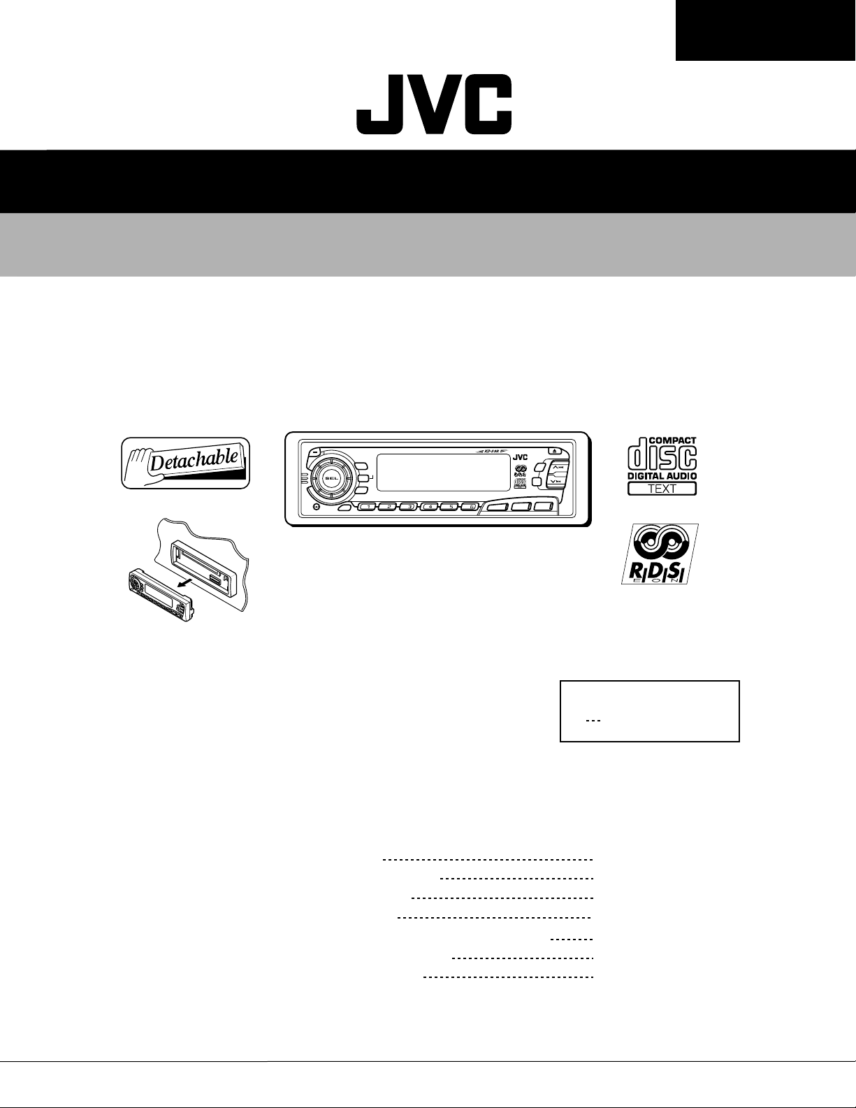
CD RECEIVER
KD-S9R
KD-S9R
Contents
A
T
T
/
/I
45Wx4
DISP
RDS
TP
PTY
789101112
SCM
MO
RND
SSM
RPT
CD
FM
AM
Area Suffix
E Continental Europe
Safety precaution
Preventing static electricity
Disassembly method
Adjustment method
Flow of functional operation unit TOC read
Maintenance of laser pickup
Description of major ICs
This service manual is printed on 100% recycled paper.
COPYRIGHT 2000 VICTOR COMPANY OF JAPAN, LTD.
1-2
1-3
1-4
1-9
1-10
1-11
1-12
No.49579
Dec. 2000
Page 2
KD-S9R
Safety precaution
CAUTION
!
CAUTION
!
Burrs formed during molding may be left over on some parts of the chassis. Therefore,
pay attention to such burrs in the case of preforming repair of this system.
Please use enough caution not to see the beam directly or touch it in case of an
adjustment or operation check.
1-2
Page 3
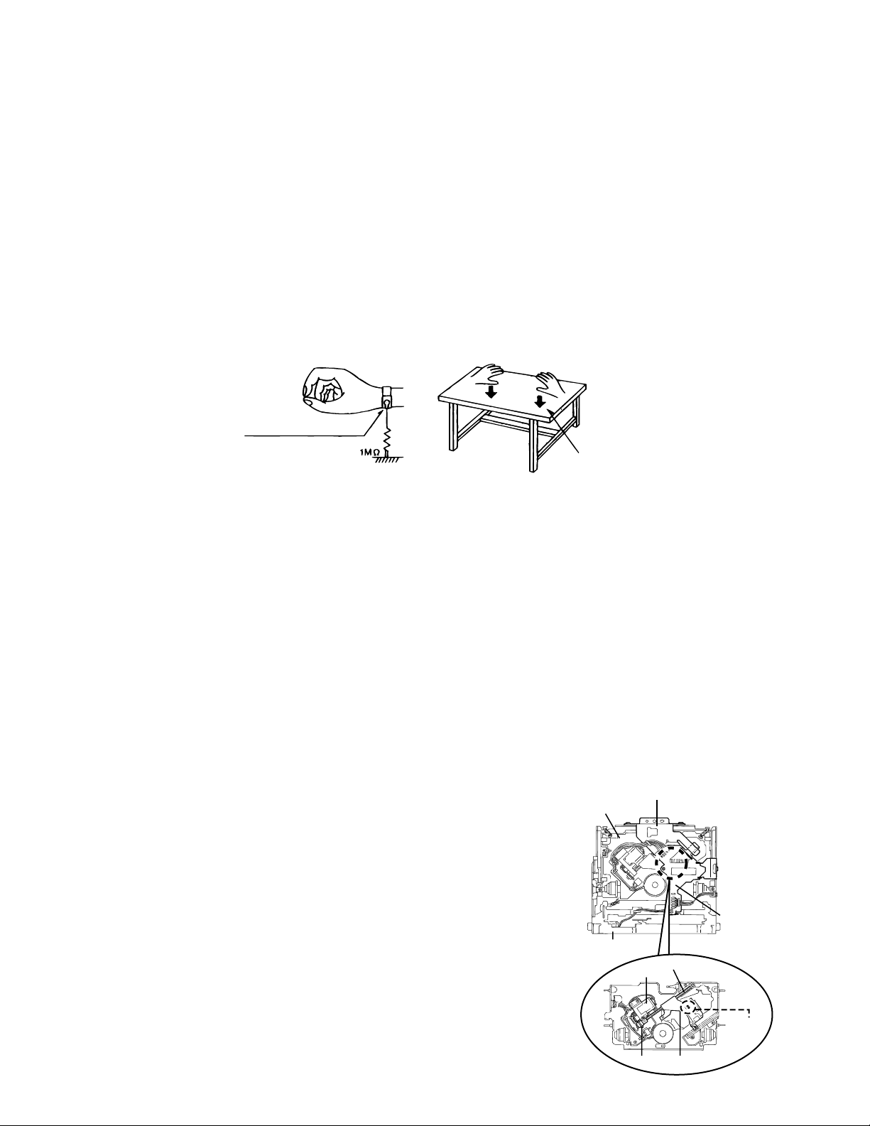
Preventing static electricity
1.Grounding to prevent damage by static electricity
Electrostatic discharge (ESD), which occurs when static electricity stored in the body, fabric, etc. is discharged,
can destroy the laser diode in the traverse unit (optical pickup). Take care to prevent this when performing repairs.
KD-S9R
2.About the earth processing for the destruction prevention by static electricity
Static electricity in the work area can destroy the optical pickup (laser diode) in devices such as CD players.
Be careful to use proper grounding in the area where repairs are being performed.
2-1 Ground the workbench
Ground the workbench by laying conductive material (such as a conductive sheet) or an iron plate over
it before placing the traverse unit (optical pickup) on it.
2-2 Ground yourself
Use an anti-static wrist strap to release any static electricity built up in your body.
(caption)
Anti-static wrist strap
Conductive material
(conductive sheet) or iron plate
3. Handling the optical pickup
1. In order to maintain quality during transport and before installation, both sides of the laser diode on the
replacement optical pickup are shorted. After replacement, return the shorted parts to their original condition.
(Refer to the text.)
2. Do not use a tester to check the condition of the laser diode in the optical pickup. The tester's internal power
source can easily destroy the laser diode.
4.Handling the traverse unit (optical pickup)
1. Do not subject the traverse unit (optical pickup) to strong shocks, as it is a sensitive, complex unit.
2. Cut off the shorted part of the flexible cable using nippers, etc. after replacing the optical pickup. For specific
details, refer to the replacement procedure in the text. Remove the anti-static pin when replacing the traverse
unit. Be careful not to take too long a time when attaching it to the connector.
3. Handle the flexible cable carefully as it may break when subjected to strong force.
4. It is not possible to adjust the semi-fixed resistor that adjusts the laser power. Do not turn it
CD mechanism ass’y
Damper bracket
Attention when traverse unit is decomposed
*Please refer to "Disassembly method" in the text for pick-up and how to
detach the substrate.
1.Solder is put up before the card wire is removed from connector on
the CD substrate as shown in Figure.
(When the wire is removed without putting up solder, the CD pick-up
assembly might destroy.)
2.Please remove solder after connecting the card wire with
when you install picking up in the substrate.
Front bracket
Feed motor ass’y
FD screw
CD mechanism
control board
Soldering
FD gear
Pickup unit
1-3
Page 4
KD-S9R
Disassembly method
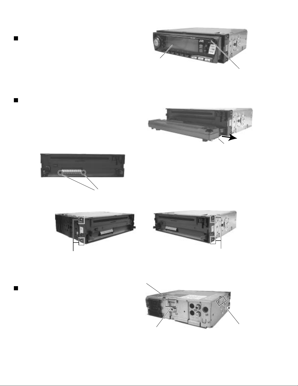
Removing the front panel unit (See Fig. 1, 2)
1.Press the Eject button to open the front panel unit
2.Push and open the right and left open/close shaft arms
outward to remove the shaft.
3.Remove the front panel unit from the same side as the
shaft was removed.
Removing the front chassis assembly (See Fig. 3, 4)
1.Remove the front panel unit.
2.Remove the two screws A attaching the front chassis
assembly.
3.Remove the four ribs a attaching the front chassis
assembly to the chassis.
Front panel unit
Eject button
Fig 1
Open/close
shaft arm
A
Fig 3
a
Removing the bottom cover assembly
(See Fig. 5)
Fig 4
b
Fig 2
a
Turn the unit upside down,then insert and turn to
b the screwdriver to remove the bottom cover.
1-4
b
b
Fig 5
Page 5
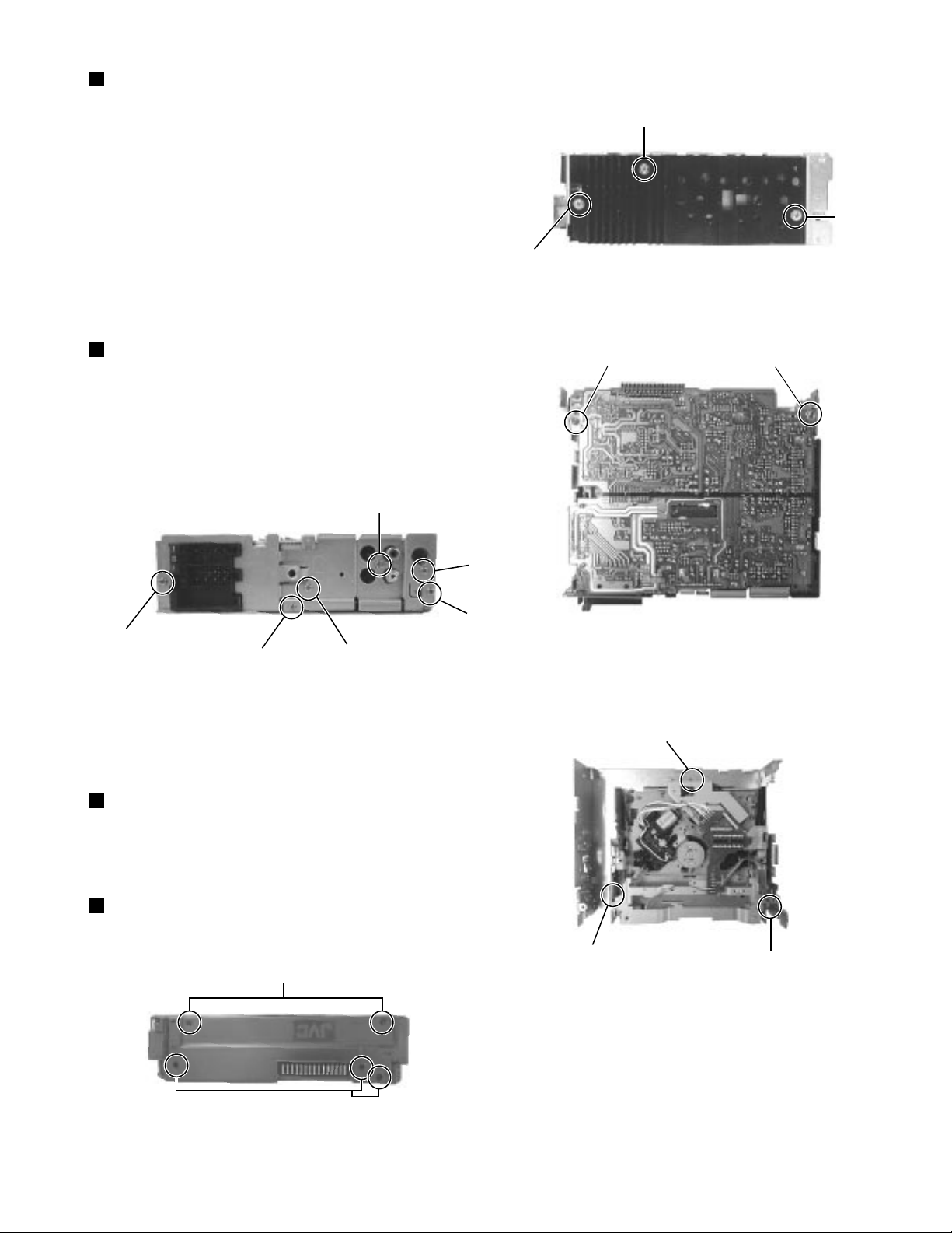
Removing the main board(wiht rear panel)
(See Fig. 6, Fig. 7)
1.Remove three screws E retaining the rear panel to the
chassis
2.Remove one screw C retaining the IC to the heat sink.
3.Remove two screws D retaining the main board.
4.Lift up the main board to remove it.
5.Remove two screws B to remove the heat sink.
KD-S9R
C
B
B
Fig 6
Removing the rear bracket (See Fig. 7)
1.Remove one screw I to remove the IC bracket.
2.Remove one screw F to remove the line-out jack.
3.Remove one screw G to remove the antenna jack.
F
E
E
I
Fig 7-2
G
E
D
D
Fig 7-1
J
CD mechanism assembly (See Fig. 8)
Remove three mechanism mounting screws J retaining the
top cover.
Front panel unit (See Fig.9)
Remove five screws K retaining the rear cover.
K
K
Fig 9
J
J
Fig 8
1-5
Page 6
KD-S9R
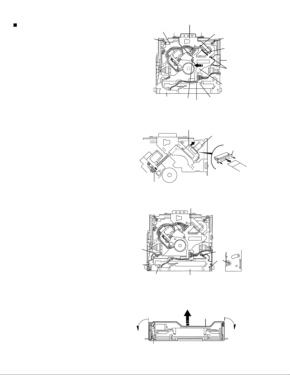
Removing the CD mechanism control
board (See Fig.1 and 2)
Unsolder the part f and g on the CD mechanism
control board.
Remove the stator fixing the CD mechanism control
board and the damper bracket (To remove the stator
smoothly, pick up the center part).
Remove the screw F attaching the CD mechanism
control board.
Remove the CD mechanism control board in the
direction of the arrow while releasing it from the two
damper bracket slots i and the front bracket slot j.
Disconnect the flexible wire from connector on the
pickup unit.
ATTENTION:
Turn the FD gear in the direction of the
arrow to move the entire pickup unit to
the appropriate position where the
flexible wire of the CD mechanism unit
can be disconnected easily (Refer to
Fig.2).
CD mechanism ass’y
m
Front bracket
Damper bracket
I
g
F
Fig.1
Pickup unit
I
j
Flexible wire
f
m
h
I
i
CD mechanism
control board
Shift the lock
k
G
Loading motor
Pull outward
FD gear
Fig.2
CD mechanism control board
Front bracket
Fig.3
Front bracket
k
G
Pull outward
1-6
Flame
Fig.4
Page 7
KD-S9R
Removing the loading motor
(See Fig.3 to 5)
*
Prior to performing the following procedure, remove
the CD mechanism control board.
1.
Remove the two springs k attaching the CD mechanism
ass’y and the front bracket.
2.
Remove the two screws G and the front bracket
while pulling the flame outward.
3.
Remove the belt and the screw H from the loading
motor.
Removing the CD mechanism ass’y
(See Fig.1, 6 to 9)
CD mechanism ass’y
I
Flame
m
Loading motor
Fig.5
I
Fig.6
H
Belt
Damper bracket
m
I
I
*
Prior to performing the following procedure, remove
the CD mechanism control PWB and the front
bracket (loading motor).
1.
Remove the three screws I and the damper bracket.
2.
Raise the both sides fix arms and move the fix plates
in the direction of the arrow to place the four shafts l
as shown in Fig.8 and 9.
3.
Remove the CD mechanism ass’y and the two
springs m attaching the flame.
4.
Remove the two screws J and both sides rear
damper brackets from the dampers. Detach the CD
mechanism ass’y from the left side to the right side.
ATTENTION:
The CD mechanism ass’y can be
removed if only the rear damper
bracket on the left side is removed.
Fix plate (L)
l
Fix arm (R)
Fig.7
Rear damper bracket
l
Fig.8
Rear damper bracket
J
Fix plate(R)
J
Fix arm (L)
Damper
Damper
l
l
Fig.9
1-7
Page 8
KD-S9R
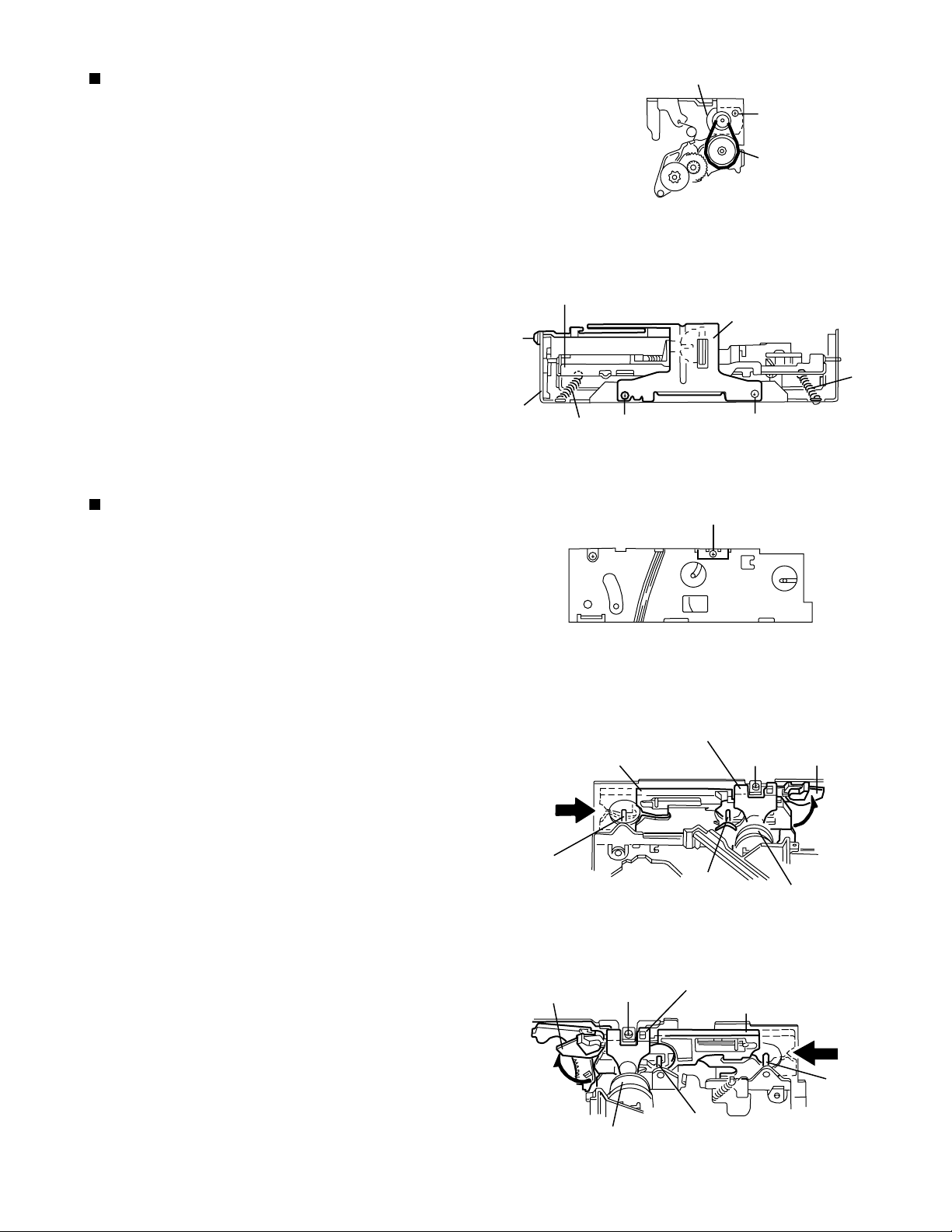
Removing the feed motor ass’y
(See Fig.10)
*
Prior to performing the following procedure, remove
the CD mechanism control board, the front bracket
(loading motor) and the CD mechanism ass’y.
1.
Remove the two screws K and the feed motor ass’y.
Removing the pickup unit
(See Fig.10 and 11)
*
*Prior to performing the following procedure, remove
the CD mechanism control board, the front bracket
(loading motor), the CD mechanism ass’y and the
feed motor ass’y.
1.
Detach the FD gear part of the pickup unit upward.
Then remove the pickup unit while pulling out the
part n of the FD screw.
Feed motor ass’y
K
FD gear
Nut push spring plate
FD screw
Pickup unit
Part n
Part O
Pickup unit
Fig.10
L
Pickup mount nut
Pickup unit
ATTENTION:
2.
Remove the screw L attaching the nut push spring
plate and the pickup mount nut from the pickup unit.
Pull out the FD screw.
When reattaching the pickup unit,
reattach the part o of the pickup unit,
then the part n of the FD screw.
Removing the spindle motor
(See Fig.12 and 13)
*
Prior to performing the following procedure, remove
the CD mechanism control board, the front bracket
(loading motor), the CD mechanism ass’y and the
feed motor ass’y.
1.
Turn up the CD mechanism ass’y and remove the
two springs p on both sides of the clamper arms.
Open the clamper arm upward.
2.
Turn the turn table, and remove the two screws M
and the spindle motor.
FD screw
p
Spindle motor
Fig.11
p
Fig.12
M
1-8
M
Fig.13
Page 9
Adjustment method
KD-S9R
Test instruments required for adjustment
1.Digital oscilloscope(100MHz)
2.AM Standard signal generator
3.FM Standard signal generator
4.Stereo modulator
5.Electric voltmeter
6.Digital tester
7.Tracking offset meter
8.Test Disc JVC:CTS-1000
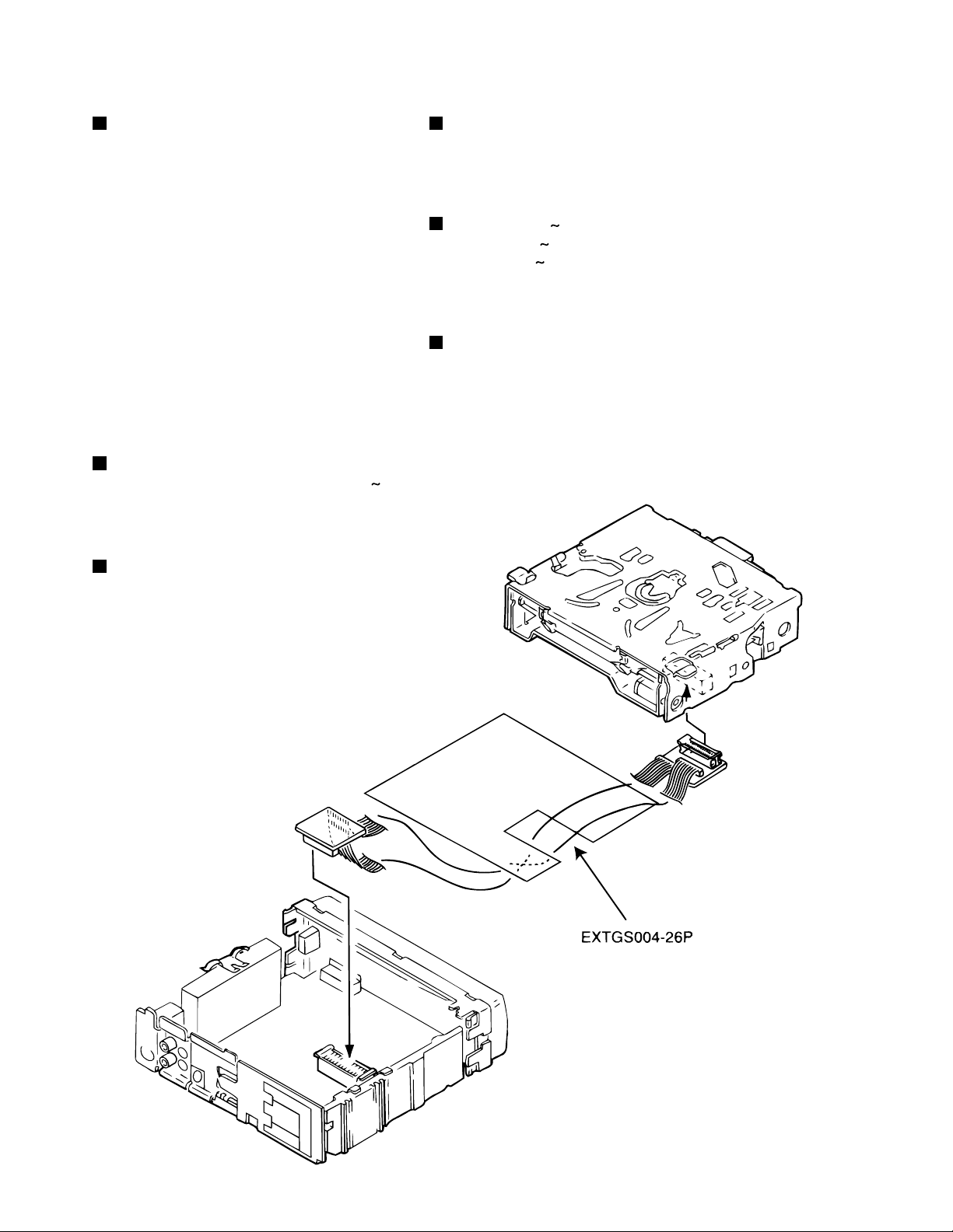
9.Extension cable for check
EXTGS004-26P x 1
Standard measuring conditions
Power supply voltage DC14.4V(10.5 16V)
Load impedance 20Kohm(2 Speakers connection)
Output Level Line out 2.0V (Vol.MAX)
How to connect the extension cable for adjusting
Standard volume position
Balance and Bass & Treble volume:Indication"0"
Loudness:OFF
BBE :OFF
Frequency Band
FM 87.5MHz 108.0MHz
MW 522kHz 1620 kHz
LW 144kHZ 279kHz
Dummy load
Exclusive dummy load should be used for AM, and FM,For
FM dummy load,there is a loss of 6dB between SSG output
and antenna input, The loss of 6dB need not be considered
since direct reading of figures are applied in this working
standard.
1-9
Page 10

KD-S9R
Flow of functional operation until TOC read
Power ON
• When the pickup correctly moves
to the inner area of the disc
Set Function to CD
• When the laser diode correctly
emits
Microprocessor
commands
FMO
TC9462 "53"
FEED MOTOR
+TERMINAL
TERMINAL
IC581 "5"
REST SW
• When correctly focused
Focus Servo Loop ON
Disc inserted
Pickup feed to the inner area
Laser emitted
Focus search
Disc rotates
RF signal eye-pattern
remains closed
Tracking loop closed
RF signal eye-pattern
opens
TOC readout
YES
YES
Microprocessor
commands
"No disc"
display
• When the disc correctly rotates
Microprocessor
commands
Spindle
motor (-)
IC581 "7"
AccelerationAcceleration
0.5 Sec
Rough
Servo
0.5 Sec
Servo CLV
1-10
Jump to the first track
Play
Tracking Servo Loop ON
• RF signal
Rough Servo Mode
CLV Servo Mode
(Program Area)
CLV Servo Mode
(Lead-In Area;
Digital: 0)
Page 11

Maintenance of laser pickup
(1) Cleaning the pick up lens
Before you replace the pick up, please try to
clean the lens with a alcohol soaked cotton
swab.
(2) Life of the laser diode
When the life of the laser diode has expired,
the following symptoms will appear.
(1) The level of RF output (EFM output:ampli tude of eye pattern) will be low.
KD-S9R
Is RF output
1.0 0.35Vp-p?
YES
O.K
(3) Semi-fixed resistor on the APC PC board
The semi-fixed resistor on the APC printed
circuit board which is attached to the pickup
is used to adjust the laser power.Since this
adjustment should be performed to match the
characteristics of the whole optical block,
do not touch the semi-fixed resistor.
If the laser power is lower than the specified
value,the laser diode is almost worn out, and
the laser pickup should be replaced.
If the semi-fixed resistor is adjusted while
the pickup is functioning normally,the laser
pickup may be damaged due to excessive current.
NO
Replace it.
Replacement of laser pickup
Turn off the power switch and,disconnect the
power cord from the ac outlet.
Replace the pickup with a normal one.(Refer
to "Pickup Removal" on the previous page)
Plug the power cord in,and turn the power on.
At this time,check that the laser emits for
about 3seconds and the objective lens moves
up and down.
Note: Do not observe the laser beam directly.
Play a disc.
Check the eye-pattern at TP1.
Finish.
1-11
Page 12

KD-S9R
Descrption of major ICs
UPD784215AGC126(IC701):DSP controller
1.Terminal layout
75 ~ 51
76
~
50
~
1-12
100
1 ~ 25
26
2.Pin function
Pin No. Symbol I/O Function
-
1~8
9
10
11
12
13
14
15
16
17
18
19
20
21
22
23
24
25~32
33
34,35
36
37,38
39
40
41
42
43
44
45,46
47
48
49
50
51,52
53
54~63
64,65
66
67
68
69,70
71
72
73~80
81
82
83
84
85
86
87
88
89
90~93
94
95~100
VDD
X2
X1
VSS
XT2
XT1
RESET
AUTODATA
LOCK
DIGITAL0
FORMAT
CHANNEL
ERR
RSTDET
AVDD
AVREF0
AVSS
RX,TX
DSPCOM
DSPSTS
DSPCLK
DSPRDY
MIDIO_IN/OUT
MICK
MICS
MILP
MIACK
DSPRST
CDTI/CDTO
CCLK
CS
XTS
PD
GND
VDD
3D-ON
3D-ON
ANA/T-TONE
REF-MIX
D.MUTE
S.MUTE
ASW1~4
TEST
I/O
I/O
Unused terminal
-
Power supply terminal
O
Crystal oscillation terminal 6.14MHz (main clock)
I
Crystal oscillation terminal 6.14MHz (main clock)
-
Connects to ground
-
Unused terminal
-
Unused terminal
I
Reset signal input
I
DSP general-purpose port output interrupt
I
DSP general-purpose port output interrupt
I
DSP general-purpose port output interrupt
I
DSP general-purpose port output interrupt
I
DSP general-purpose port output interrupt
I
DSP general-purpose port output interrupt
I
DSP general-purpose port output interrupt
-
Power supply terminal
-
Connects to ground
-
Connects to ground
-
Connects to ground
-
Unused terminal
-
Power supply terminal
-
Unused terminal
-
Unused terminal
I
Communication port with IC401
O
Status communication port to IC401
I
Clock input from IC401
I
Ready signal input from IC401
-
Unused terminal
DSP-microcomputer I/F
O
Clock signal to IC631
O
Chip selection to IC631
O
DSP-microcomputer I/F
O
DSP-microcomputer I/F
-
Unused terminal
O
Output of reset signal of DSP
-
Unused terminal
CODEC-microcomputer I/F
O
Clock signal to IC601
O
Chip selection to IC601
O
OSC selection
-
Unused terminal
O
Reset signal output
-
Connects to ground
-
Unused terminal
-
Power supply terminal
-
Unused terminal
O
Switches at the output destination of the surround channel
O
Test tone control
O
Control at output destination of LFE channel
-
Unused terminal
O
MUTE of digital out terminal
O
Audio signal MUTE
-
Unused terminal
O
Digital input selection
-
Test terminal
-
Unused terminal
Page 13

TEA6320T-X (IC161) : E.volume
1.Pin layout
2.Block diagram
10 8 9 7 6
KD-S9R
5
12
SDA
1
GND
2
OUTLR
OUTLF
MUTE
TL
B2L
B1L
IVL
ILL
QSL
IDL
ICL
IMD
IBL
IAL
3
4
5
6
7
8
9
10
11
12
13
14
15
16
3.Pin functions
Pin
Symbol
No.
SDA
1
SCL
32
VCC
31
OUTRR
30
OUTRF
29
TR
28
B2R
27
B1R
26
IVR
25
ILR
24
QSR
23
IDR
22
Vref
21
ICR
CD-CH
TAPE
TUNER
20
19
18
17
CAP
IBR
IAR
I/O
Serial data input/output.
I/O
MUTE
21
31
2
19
16
15
13
11
14
22
20
18
17
Functions Functions
POWER
SUPPLY
SOURCE
SELECTOR
23 25 24 26 27 28
VOLUME 1
+20 to -31 dB
LOUDNESS
LEFT
VOLUME 1
+20 to -31 dB
LOUDNESS
RIGHT
Pin
No.
17
Symbol
IAR
BASS
LEFT
+15 dB
LOGIC
BASS
RIGHT
+15 dB
I/O
I
Input A right source.
TREBLE
LEFT
+12 dB
TREBLE
RIGHT
+12 dB
FUNCTION
ZERO CROSS
DETECTOR
VOLUME 2
0 to 55 dB
BALANCE
FENDER REAR
VOLUME 2
0 to 55 dB
BALANCE
FENDER FRONT
HC BUS
REC
VOLUME 2
0 to -55dB
BALANCE
FENDER FRONT
VOLUME 2
0 to -55dB
BALANCE
FENDER REAR
3
4
32
1
29
30
2
3
4
5
6
7
8
9
10
11
12
13
14
15
16
GND
OUTLR
OUTLF
TL
B2L
B1L
IVL
ILL
QSL
IDL
MUTE
ICL
IMO
IBL
IAL
Ground.
-
output left rear.
O
output left front.
O
Treble control capacitor left channel or
I
input from an external equalizer.
Bass control capacitor left channel or
-
output to an external equalizer.
Bass control capacitor left channel.
-
Input volume 1. left control part.
I
Input loudness. left control part.
I
Output source selector. left channel.
O
Not used
-
Not used
-
Input C left source.
I
Not used
-
Input B left source.
I
Input A left source.
I
18
19
20
21
22
23
24
25
26
27
28
29
30
31
32
IBR
CAP
ICR
Vref
IDR
QSR
ILR
IVR
B1R
B2R
TR
OUTRF
OUTRR
Vcc
SCL
I
Input B right source.
-
Electronic filtering for supply.
I
Input C right source.
-
Reference voltage (0.5Vcc)
-
Not used
O
Output source selector right channel.
I
Input loudness right channel.
I
Input volume 1. right control part.
-
Bass control capacitor right channel
Bass control capacitor right channel or
O
output to an external equalizer.
Treble control capacitor right channel or
I
input from an external equalizer.
O
Output right front.
O
Output right rear.
-
Supply voltage.
I
Serial clock input.
1-13
Page 14

KD-S9R
BA4905-V3 (IC901) : Regulator
1.Terminal layout
12 34 56 78 9101112
2.Block diagram
REGULATOR
EXT
OIVPC
RESET
1 2 3 4 5 6 7 8 9 10 11 12
RESET COMP VDD 5.7V CD 8V VCC AJ
EXT ACC AUDIO 9V CTRL ILM 10V GND
37K
5K
1-14
Page 15

KD-S9R
Explanation of terminals
1
2
2
4
5
6
7
8
9
RESET
EXT output
COMP output
ACC
VDD output
AUDIO output
CD output
CTRL
VCC
BA4905-V3
If VDD voltage becomes 4V or less, RESET output becomes low level.
This outout voltage is approximately 0.5V lower than VCC, and max
output current is 300mA.
A voltage supply for ACC block this outout voltage is approximately
0.7V lower than VDD'S. The max output current is 100mA.
Control of the COMP output by inputting voltage.
This output voltage is 5.7V, and max output current is 100mA.
This voltage supply is for microcomputer. Whenever block up voltage
supply is connected. the output keeps on running.
This output voltage is 9.0V, and max output current is 500mA.
This voltage supply for AUDIO.
This output voltage is 8.0V, and max output current is 1A.
This voltage supply for CD.
Output selector of CD, AUDIO,ILM and EXT.
To be connected with the BACK UP of car.
10
11
12
ILM output
AJ
GND
This output voltage is 10V, and max output current is 500mA.
Output voltage is adjustable.
Putting a resistance between ILM and AJ or between AJ and GND
makes ILM output voltage adjustable.
Ground.
1-15
Page 16

KD-S9R
LA4743B(IC301):Power AMP
1.Block diagram
IN 1
TA B
IN 2
+
0.22 F
+
0.22 F
11
1
12
Vcc 1/2 Vcc 3/4
6 20
-
+
Protective
circuit
-
+
2200 F 0.022 F
+
9
7
+
OUT 1+
OUT 1-
PWR GND1
8
+
OUT 2+
5
-
OUT 2-
3
PWR GND2
2
ST BY
R.F
47 F
IN 3
PRE GND
IN 4
+5V
ST ON
+
0.22 F
N.C
+
0.22 F
4
Stand by
Switch
Mute
10
+
Ripple
Filter
Mute
22
circuit
3.3 F
+
15
-
+
-
17
19
10K
+
OUT 3+
OUT 3-
Low Level
Mute ON
25
18
24
23
PWR GND3
OUT 4+
OUT 4-
13
14
Protective
circuit
-
+
+
-
1-16
ON TIME C
22 F
Muting &
16
+
ON Time Control
Circuit
PWR GND4
24
Page 17

2.Terminal layout
3.Pin function
1
2
3
4
5
6
7
8
9
10
11
12
13
14
15
16
17
18
19
20
21
22
23
24
25
SymbolPin No. Function
TA B
GND
OUTRRSTBY
OUTRR+
VCC1/2
OUTRFGND
OUTRF+
RIPPLE
INRF
INRR
SGND
INLR
INLF
ONTIME
OUTLF+
GND
OUTLFVCC3/4
OUTLR+
MUTE
OUTLRGND
NC
Header of IC
Power GND
Outpur(-) for front Rch
Stand by input
Output (+) for front Rch
Power input
Output (-) for rear Rch
Power GND
Output (+) for rear Rch
Ripple filter
Rear Rch input
Front Rch input
Signal GND
Front Lch input
Rear Lch input
Power on time control
Output (+) for rear Lch
Power GND
Output (-) for rear Lch
Power input
Output (+) for front
Muting control input
Output (-) for front
Power GND
Non connection
KD-S9R
LA4743B
1-17
Page 18

KD-S9R
LA6567H-X(IC501):CD DRIVE
1.Pin layout & blockdiagram
VCC2
V05-
V05+
V04+
V04-
V03+
V03-
FR
1
2
3
4
5
6
7
FR
CH 3,4,5
Power supply
CH5
CH4
CH3
Thermal shutdown
Output control
Level shiftLevel shiftLevel shiftLevel shift
Input
22K 11K
Signal system power supply
28
27
26
25
24
23
22
FR
REV
FWD
S-GND
VCONT
VIN4
VIN4G
VCC-S
FR
VC2+
V02-
V01+
V01-
VCC1
VIN1
VIN1G
8
9
10
11
12
13
14
CH2
CH1
CH1,2
Power supply
11K
22K
5VREG(PNPTr
The outside puuting)
22K
11K
22K
11K
21
20
19
18
17
16
15
VREF-IN
REG-OUT
REG-IN
VIN3G
VIN3
VIN2G
VIN2
1-18
Page 19

KD-S9R
2. Pin function
Pin no. Symbol
1
2
3
4
5
6
7
8
9
10
11
12
13
14
15
16
17
18
19
20
21
22
23
24
25
26
27
28
VCC2
V05V05+
V04+
V04V03+
V03V02+
V02V01+
V01-
VCC1
VIN1
VIN1G
VIN2
VIN2G
VIN3
VIN3G
REG-IN
REG-OUT
VREF-IN
VCC-S
VIN4G
VIN4
VCONT
S-GND
FWD
REV
LA6567H-X(2/2)
Function
CH3,4,5 Power supply( It is short with VCC1,VCC-S)
Loading output(-)
Loading terminal (+)
CH4 Output terminal(+)
CH4 Output terminal(-)
CH3 Output terminal(+)
CH3 Output terminal(-)
CH2 Output terminal(+)
CH2 Output terminal(-)
CH1 Output terminal(+)
CH1 Output terminal(-)
CH1,2(BTL) Power supply(It is short with VCC-S,VCC2)
CH1 Input terminal
CH1 Input terminal(For gain adjustment)
CH2 Input terminal
CH2 Input terminal(For gain adjustment)
CH3 Input terminal
CH3 Input terminal(For gain adjustment)
Regulator terminal(Outside putting PNP base)
Regulator terminal(Outside putting PNP collector)
Standard voltage input terminal
Signal system power supply(It is short with VCC1,VCC2)
CH4 Input terminal(For gain adjustment)
CH4 Input terminal
5CH(VLO) Output voltag set terminal
Signal system GND
5CH(VLO)Signal output switch terminal(FWD),Input of logic of loading part
5CH(VLO)Signal output switch terminal(REV),
Input of logic of loading part
Frame(FR)at the center bocomes system GND power.
Please be short-circuited on the outside and use the terminal of the power supply system
and three teminals of VCC-S, VCC1,VCC2.
1-19
Page 20

KD-S9R
TC9462F(IC541):
1.Pin layout & Block Diagram
RST
DD
XV
80
79
81DV
SR
82RO
83DV
DD
84DVR
85LO
86DV
SL
87TEST1
88TEST2
89TEST3
90BUS0
91BUS1
92BUS2
93BUS3
94V
DD
95V
SS
96BUCK
97CCE
98TEST4
99TSMOD
100
1 2 3
TEST0
XO78XI
LPF
HSO
Micon
interface
UHSO
SS
XV
77
4 5
EMPH
DD
V
75
76
1bit
DAC
PXO
SS
PXI
V
74
73
Clock
generator
Correction
circuit
Audio out
circuit
6
7 8 9 10 11 12 13
SS
V
BCK
LRCK
AOUT
72
TESIO1
DOUT
71
TESIN
MBOV
DACT
69
70
Address circuit
16KRAM
Digital out
IPF
CKSE
SBOK
DMOUT
68
CLCK
IO3
IO265IO164IO063V
67
66
ROM
Automatic adjustment
RAM
Synchronous
guarantee
EFM decode
Sub code
decoder
14 15
16 17 18 19 20 21 22
SS
DD
V
V
DATA
SFSY
SS
DD
V
61
62
Servo
control
Digital equalizer
circuit
CLV servo
SBSY
SPCK
FLGD60FLGC59FLGB58FLGA57SEL562V
PWM D/A
A/D
Status
TMAX
23 24 25
DD
COFS
MONIT
V
TESIO0
SPDA
REF
DMO54FVO53FMO52TEBC51RFGC
55
+
-
Data
slicer
VCO
PLL
26
27 28
REF
ZDET
HSSW
P2V
+
PDO
50 V
REF
49 TRO
48 FOO
TEZI
+
TMAXS
30
TMAX
47
46 TEI
45 TSIN
44 SBAD
43 FEI
42 RFRP
41 RFZI
40 RFCT
39 AV
DD
38 RFI
37 SLCO
36 AV
SS
35 VCOF
34 VCOREF
33 PV
REF
32 LPFO
31 LPFN
+
-
-
-
29
2.Pin function
PIN No.
1
2
3
4
5
6
7
8
9
10
11
12
13
14
15
16
17
18
19
20
21
22
23
24
25 P2V
SYMBOL
TEST0
HSO
UHSO
EMPH
LRCK
V
SS
BCK
AOUT
DOUT
MBOV
IPF
SBOK
CLCK
V
DD
V
SS
DATA
SFSY
SBSY
SPCK
SADA
COFS
MONIT
V
DD
TESIO0--I
REF
FUNCTIONAL DESCRIPTION
I/O
Test mode terminal.Normally, Keep at open.
I
Playback speed mode fllag output terminal.
UHSO
HSO
O
H
H
L
O
Subcode Q data emphasis flag output terminal.Emphasis ON at "H" level and OFF at "L"
O
level.The output polarity can invert by command.
Channel clock output terminal.(44.1khz)L-ch at "L" level and R-ch at "H" level. the output
O
polarity can invert by command.
Digital GND terminal.
-O
Bit clock output terminal.(1.4122MHz)
Audio data output terminal.
O
Digital data output terminal.
O
Buffer memory over signal output terminal. Over at "H" level.
O
Correction flag output terminal. At "H" level,AOUT output is made to correction
O
impossibility by C
Subcode Q data CRCC check adjusting result output terminal.
O
The adjusting result is OK at "H" level.
Subcode P W data reabout clock input/output terminal.
I/O
This terminal can select by command bit.
--
Digital power supply voltage terminal.
--
Digital GND terminal.
O
Subcode P W data output terminal.
O
Play-back frame sync signal output terminal.
O
Subcode block sync signal output terminal.
O
Processor status signal reabout clock output terminal.
O
Processor status signal output terminal.
O
Correction frame clock output terminal. (7.35kHz)
Internal signal (DSP internal flag and PLL clock) output terminal.Selected by command.
O
This terminal output the text data with serial by command.
L
PLAYBACK SPEED
H
L
H
Nomal
2 times
4 times
L
2
correction processing.
--
Digital power supply voltage terminal.
Test input/output terminal.Normally,keep at "L" level.
The terminal that inputted the clock for read of text data by command.
--
PLL double reference voltage supply terminal.
REMARKS
With pull-up resistor.
--
--
--
--
--
--
--
--
--
--
--
--
--
--
--
--
--
--
--
--
--
--
--
1-20
Page 21

KD-S9R
2.Pin Function (2/2)
Pin No.
40
41
42
43
44
45
46
47
48
49
50
51
52
53
54
55
56
57
58~61
62
63
64~67
68
69
70
71
72
73
74
75
76
77
78
79
80
81
82
83
84
85
86
87~89
90~93
94
95
96
97
98
99
100
Symbol
RFCT
RFZI
RFRP
FEI
SBAD
TSIN
TEI
TEZI
FOO
TRO
VREF
RFGC
TEBC
FMO
FVO
DMO
2VREF
SEL
FLGA~D
VDD
VSS
IO0~3
DMOUT
CKSE
DACT
TESIN
TESIO1
VSS
PXI
PXO
VDD
XVSS
XI
XO
XVDD
DVSR
RO
DVDD
DVR
LO
DVSL
TEST1~3
BUS0~3
VDD
VSS
BUCK
CCE
TEST4
TSMOD
RST
I/O
RFRP signal center level input terminal
I
RFRP zero cross input terminal
I
RF ripple signal input terminal
I
Focus error signal input terminal
I
Sub-beam adder signal input terminal
I
Test input terminal Normally, keep at "vref" level
I
Tracking error signal input terminal. Take in at tracking servo ON.
I
Tracking error zero cross input terminal
I
Focus servo equalizer output terminal
O
Tracking servo equalizer output terminal
O
Analog reference voltage supply terminal
RF amplitude adjustment control signal output terminal
O
Tracking balance control signal output terminal
O
Feed equalizer output terminal
O
Speed error signal or feed search equalizer output terminal
O
Disk equalizer output terminal
O
Analog double reference voltage supply terminal
APC circuit ON/OFF indication signal output terminal
O
External flag output terminal for internal signal
O
Digital power supply voltage terminal
Digital GND terminal
General I/O terminal
I/O
This terminal control IO0~IO3 terminal
I
Normally, keep at open
I
DAC test mode terminal. Normally, keep at open
I
Test input terminal, Normally, keep at "L" level
I
Test input/output terminal. Normally, keep at "L" level
I
Digital GND terminal
Crystal oscillator connecting input terminal for DSP
I
Crystal oscillator connecting output terminal for DSP
O
Digital power supply voltage terminal
Oscillator GND terminal for system clock
Crystal oscillator connecting input terminal for system clock
I
Crystal oscillator connecting output terminal for system clock
O
Oscillator power supply voltage terminal for system clock
Analog GND terminal for DA converter (Rch)
R channel data forward output terminal
O
Analog supply voltage terminal for DA converter
Reference voltage terminal for DA converter
L channel data forward output terminal
O
Analog GND terminal for DA converter (Lch)
Test mode terminal . Normal keep at open
I
Micon interface data input/output terminal
I/O
Digital power supply voltage terminal
Digital GND terminal
Micon interface clock input terminal
I
Command and data sending/receiving chip enable signal input terminal
I
Test mode terminal. Normal, keep at open
I
Local test mode selection terminal
I
Reset signal input terminal. Reset at "L" level
I
Function
(PWM carrier=88.2kHz for DSP, Synchronize to PXO)
TC9462F
1-21
Page 22

KD-S9R
BA3880FS-X(IC181) : BBE
1. Pin layout & Block Diagram
GND
1
DETR
DEFR
2
CTL
3
CTL
24
23
22
DETL
DEFL
CTL
VCAR
MIXR
OUTR
INR
APFR
HPFR
LPFR
BIASC
10
11
12
4
5
6
7
8
9
VCA
HPF
LPF
+
+
HI MID
+
+
+
+
-
+
+
HI
LO
+
VCA
+
+
+
MID
+
+
LO
+
+
-
LPF
HPF
21
20
19
18
17
16
15
14
13
Vcc
VCAL
MIXL
OUTL
INL
APFL
HPFL
LPFL
2. Pin Functions
Pin
Symbole Function Symbole Function
No.
10
11
12
GND
1
DETR
2
DEFR
3
CTL
4
VCAR
5
MXIR
6
OUTR
7
8
APFR
9
HPFR
LPFR
BIAS
Grounding terminal
Peak level detector output for treble VCA control
Control signal time constant terminal
Control signal input terminal
Treble CA output terminal
Output MIX amplifier summing terminal
Signal output terminal
INR
Signal input terminal
Input inversion amplifier output terminal
HPF output terminal
LPF output terminal
Reference voltage output terminal (1/2 Vcc)
Pin
No.
13
14
15
16
17
18
19
20
21
22
23
24
LPFL
HPFL
APFL
INL
OUTL
MIXL
VCAL
VCC
DEFL
DETL
LPF output terminal
HPF output terminal
Input inversion amplifier output terminal
Non connector
Signal input terminal
Signal output terminal
Output MIX amplifier summing terminal
Treble CA output terminal
Power supply terminal
Control signal time constant terminal
Non connector
Peak level detector output for treble VCA control
1-22
Page 23

BA6218 (IC591) : Motor driver
KD-S9R
1. Block diagram
7
OUT 2
12k
6 Vcc
9 OUT1
6.8k 6.8k
12k
3
RIN
2. Function truth table
3Pin (IN)
20k
1Pin (IN)
H
L
H
L
L
H
H
L
528
GND GND COM
7Pin (OUT)
H
H
L
OPEN
9Pin (OUT)
OPEN
1 FIN
20k
H
L
L
1-23
Page 24

KD-S9R
HD74HC126FP-X (IC801) : Buffer
1.Terminal layout
1
2
3
4
5
6
7
2.Block diagram
Input
14
13
12
11
10
9
8
Vcc Vcc
1A
2A
3A
4A
1C
2C
3C
See Function Table
4C
3.Pin function
Output
1Y
2Y
Output
2Y
Output
3Y
Output
4Y
Input Outout
C
A
L
X
H
L
H
H
1k
CL
Sample as Load Circuit 1
Sample as Load Circuit 1
Sample as Load Circuit 1
Y
Z
H
L
S1
1k
1-24
Page 25

SAA6579T-X(IC71):RDS Detector
KD-S9R
1.Terminal Layout
QUAL
RDDA
MUX
VDDA
GND
SCOUT
Vref
CIN
1
2
3
4
5
6
7
8
16
15
14
13
12
11
10
9
RDCL
T75
OSCO
OSC1
VDD
GND
TEST
MODE
2.Pin Function
Pin
No.
1
2
3
4
5
6
7
8
9
10
11
12
13
14
15
16
QUAL
RDDA
Vref
MUX
VDDA
GND
CIN
SCOUT
MODE
TEST
GND
VDD
OSC1
OSC0
T75
RDCL
FunctionI/OSymbol
Non connect
RDS data output
O
Reference voltage output
O
Multiplex signal input
I
+5V Supply voltage for analog
Ground for analog part (0V)
Sub carrier output of reconstruction filter
I
Ground for digital part (0V)
O
Ground for digital part (0V)
Ground for digital part (0V)
Ground for digital part (0V)
+5V supply voltage for digital part
Oscillator input
I
Oscillator output
O
Non connect
RDS clock output
O
3.Block Diagram
4
8
7
5
3
ANI-
ALLUDING
FILTER
CLOCKED
COMPARATOR
REFERENCE
VOLTAGE
1413
5kHz
BAND PASS
(8th ORDER)
COSTAS LOOP
VARIABLE AND
FIXWD DIVIDER
CLOCK
REGENERATION
AND SYNC
6
RECONSTRUCTION
FILTER
BIPHASE
DECODER
TEST LOGIC AND OUTPUT
OSCILLATOR
AND
DIVIDER
SYMBOL
SELECTOR SWITCH
9
10
12
DUALITY BIT
GENERATOR
DIFFERENTIAL
DECODER
11
1
2
16
15
1-25
Page 26

KD-S9R
TA2109F-X (IC521) : RF amp.
1. Pin layout
24 13
112
2. Block diagram
SBAD
13
FEO
14
10pF
FEN
15
VRO
16
RFRP
17
RFIS
18
RFGO
19
10k ohm
21k ohm
20k ohm
20k ohm
50k ohm
36pF
7.96k ohm
50uA
20k ohm
15k ohm 30k ohm
15k ohm
20uA
10k ohm
21k ohm
12k ohm
12k ohm
PEAK
BOTTOM
10k ohm
10k ohm
30k ohm
21k ohm 29k ohm
24k ohm 24k ohm
180k ohm
1.74k ohm
20pF
65uA
10k ohm
47k ohm
SW3
13k ohm
7.67k ohm
3 STATE
DET.
SW1
1k ohm
SW2
680 ohm
2.12k ohm
LCD
20pF
TEO
TEN
2VRO
TEB
SEL
LDO
MDI
12
11
10
9
8
7
6
3. Pin function
Pin
Symbol I/O
No.
Vcc
FNI
FPI
TPI
TNI
MDI
SEL
I
I
I
I
I
O
I
I
O
I
O
10
11
12
1
2
3
4
5
6
7
8
9
LDO
TEB
2VRO
TEN
TEO
RFGC
20
AGCI
21
re=130 ohm
RFO
22
GND
23
RFN
24
23.5k ohm
3.3k ohm
12k ohm
1.53k ohm
3.3k ohm
Pin function
Power supply input terminal
Main beam I-V amp input terminal
Main beam I-V amp input terminal
Sub beam I-v input terminal
Sub beam I-V input terminal
Monitor photo diode amp input terminal
Laser diode amp output terminal
Laser diode control signal input terminal
T. error balance adj. signal input terminal
Reference voltage output terminal
TE amp negative input terminal
TE error signal output terminal
180k ohm
40pF
180k ohm
Pin
No.
13
14
15
16
17
18
19
20
21
22
23
24
180k ohm
20pF
60k ohm
60k ohm
40pF
Symbol I/O
SBAD
FEO
O
O
FEN
VRO
O
RFRP
O
RFIS
RFGO
O
RFGC
AGCI
RFO
O
GND
-
RFN
TNI
TPI
FPI
FNI
Vcc
5
4
3
2
1
I-I
I-I
20k ohm
20k ohm
20k ohm
20k ohm
Pin function
Sub beam adder signal output terminal
Focus error signal output terminal
FE amp negative input terminal
I
Reference voltage (VREF) output terminal
Track count signal output terminal
RFRP detect circuit input terminal
I
RF gain signal output terminal
RF amplitude adj. control signal input terminal
I
RF signal amplitude adj. amp input terminal
I
RF signal output terminal
Ground terminal
RF amp negative input terminal
I
1-26
Page 27

TB2118F-X (IC31) : PLL
1.Terminal Layout
2423222120191817161514
KD-S9R
13
2.Block diagram
osc
2
1
XO
24
XI
FM VCO
AMVCO
IFC
CE
DIN
DOUT
DIMM
15
16
13
3
4
5
6
123456789
Buff.
ON/OFF
OSC circuit
AMP
AMP
AMP
Serial
Interface
101112
Reference Counter
Prescaler
20-bit BINARY COUNTER
Resistor 1
Resistor 2
I/O PORT
Swallow counter
Phase
Comparator
4-bit
12-bit
Programmable counter
22-bit
40bit shift register
OUTPUT PORT
Constant
power supply voltage
switch
Vdd
switch
Vcc
AM CP.
20
+
+
-
REG.
22
19
vt
18
FM cp
3.Pin Function
Pin
Symbol I/O Function
No.
XOUT
10
11
12
1
2
3
4
5
6
7
8
9
OSC
CE
DI
CK
DOUT
SR
I/01
I/02
OUT1
OUT2
VDD2
Crystal oscillator pin
O
Non connect
Chip enable input
I
Serial data input
I
Clock input
I
Serial data output
O
Register control pin
O
I/O ports
I/O
I/O ports
I/O
Non connect
Non connect
Single power supply for REF. frequency block
-
7
SL
8
9
I/O -2I/O -1
10 11
12
out-2out-1
vdd2
Pin
Symbol I/O Function
No.
IFC
13
VDD
14
FMIN
15
AMIN
16
DGND
17
FMCP
18
VT
19
AMCP
20
VCC
21
RF
22
AGND
23
XIN
24
17
14
IF signal input
I
Power pins for digital block
FM band local signal input
I
AM band local signal input
I
Connect to GND (for digital circuit)
Charge pump output for FM
O
Tuning voltage biased to 2.5V.
Charge pump output for AM
O
Power pins for analog block
Ripple filter connecting pin
I
Connect to GND (for analog circuit)
Crystal oscillator pin
I
21
23
a-gnd
vccd-gndvdd
1-27
Page 28

KD-S9R
NJM2100M-WE (IC861) : Cruise
1. Pin layout
2. Block diagram
-INPUT
+INPUT
A OUTPUT
A -INPUT
A +INOUT
V-
1
2
3
4
V+
8
B OUTPUT
7
B -INPUT
6
B +INPUT
5
V+
OUTPUT
NJM4565M-WE (IC581,IC171) : Ope. amp
A OUTPUT
-
A INPUT
+
A INPUT
1
2
3
-
4
V
+
8
V
B OUTPUT
7
-
B INPUT
6
5
+
B INPUT
V-
1-28
Page 29

IC-PST600M/G/-W1197(IC702):Reset
1.Terminal layout
2.Block diagram
Co1
OP1
KD-S9R
Vcc
1
Vout
3
M24C16-WMN6-X(IC771):EPROM
1.Terminal layout 2.Block diagram
CONTROL
LOGIC
SDA SCL
VCC
Vss
I/O
WP
MEMORY
CONTROL
LOGIC
XDEC
GND
2
HV GENERATOR
EEPROM ARRAY
(8x 256 x8)
PAGE LATCHES
SENSE AMP
F/W CNTROL
YDEC
3.Pin function
Pin No.
1 3
Symbol Function
A0 A2
4
5
6
7
8
GND
SDA
SCL
WPIN
Vdd
No internal connection
+2.5V to 5.5V Power supply
Write protect input
Serial clock
Serial address / data I/O
Ground
1-29
Page 30

KD-S9R
VICTOR COMPANY OF JAPAN, LIMITED
MOBILE ELECTRONICS DIVISION
PERSONAL & MOBILE NETWORK BUSINESS UNIT. 10-1,1Chome,Ohwatari-machi,Maebashi-city,Japan
(No.49579)
Printed in Japan
200012 (V)
 Loading...