

Page 1
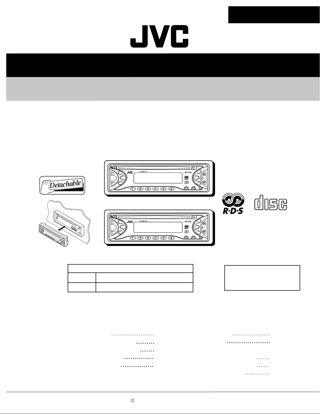
KD-S723R/KD-S721R
SERVICE MANUAL
CD RECEIVER
KD-S723R/KD-S721R
KD-S723R
TP/PTY
SEL
DISP
87 9
10 11
KD-S721R
TP/PTY
SEL
DISP
87 9
10 11
Difference point
KD-S723R LCD Color,Button Illumination--- Amber
KD-S721R LCD Color,Button Illumonation--- Green
Contents
FM
¢
CD
4
RNDRPTMO
12
RNDRPTMO
12
AM
SCMMODE
COMPACT
DIGITAL AUDIO
FM
¢
CD
4
AM
SCMMODE
Area Suffix
E -------- Continental Europe
EX ------------ Central Europe
Safety precaution
Preventing static electricity
Important for laser products
Location of main parts
Disassembly method
COPYRIGHT 2002 VICTOR COMPANY OF JAPAN, LTD.
1-2
1-3
1-4
1-5
1-6
Adjustment method
Flow of functional
operation unit TOC read
Maintenance of laser pickup
Replacement of laser pickup
Description of major ICs
1-11
1-12
1-14
1-14
1-15
No.49693
Feb. 2002
Page 2
KD-S723R/KD-S721R
Safety precaution
!
!
Burrs formed during molding may be left over on some parts of the chassis. Therefore,
pay attention to such burrs in the case of preforming repair of this system.
Please use enough caution not to see the beam directly or touch it in case of an
adjustment or operation check.
1-2
Page 3
KD-S723R/KD-S721R
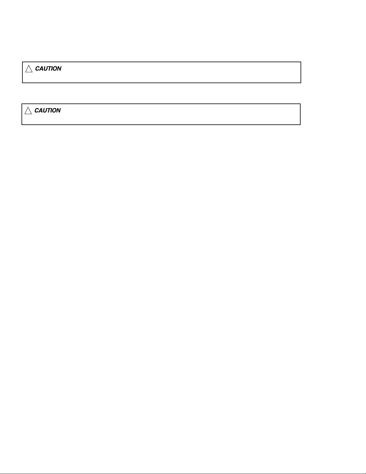
Preventing static electricity
Electrostatic discharge (ESD), which occurs when static electricity stored in the body, fabric, etc. is discharged,
can destroy the laser diode in the traverse unit (optical pickup). Take care to prevent this when performing repairs.
1.1. Grounding to prevent damage by static electricity
Static electricity in the work area can destroy the optical pickup (laser diode) in devices such as DVD players.
Be careful to use proper grounding in the area where repairs are being performed.
1.1.1. Ground the workbench
1. Ground the workbench by laying conductive material (such as a conductive sheet) or an iron plate over
it before placing the traverse unit (optical pickup) on it.
1.1.2. Ground yourself
1. Use an anti-static wrist strap to release any static electricity built up in your body.
(caption)
Anti-static wrist strap
Conductive material
(conductive sheet) or iron plate
1.1.3. Handling the optical pickup
1. In order to maintain quality during transport and before installation, both sides of the laser diode on the
replacement optical pickup are shorted. After replacement, return the shorted parts to their original condition.
(Refer to the text.)
2. Do not use a tester to check the condition of the laser diode in the optical pickup. The tester's internal power
source can easily destroy the laser diode.
1.2. Handling the traverse unit (optical pickup)
1. Do not subject the traverse unit (optical pickup) to strong shocks, as it is a sensitive, complex unit.
2. Cut off the shorted part of the flexible cable using nippers, etc. after replacing the optical pickup. For specific
details, refer to the replacement procedure in the text. Remove the anti-static pin when replacing the traverse
unit. Be careful not to take too long a time when attaching it to the connector.
3. Handle the flexible cable carefully as it may break when subjected to strong force.
4. It is not possible to adjust the semi-fixed resistor that adjusts the laser power. Do not turn it
Short circuit land
FD screw
Feed motor ass’y
Shorting
FD gear
Pickup unit
1-3
Page 4
KD-S723R/KD-S721R
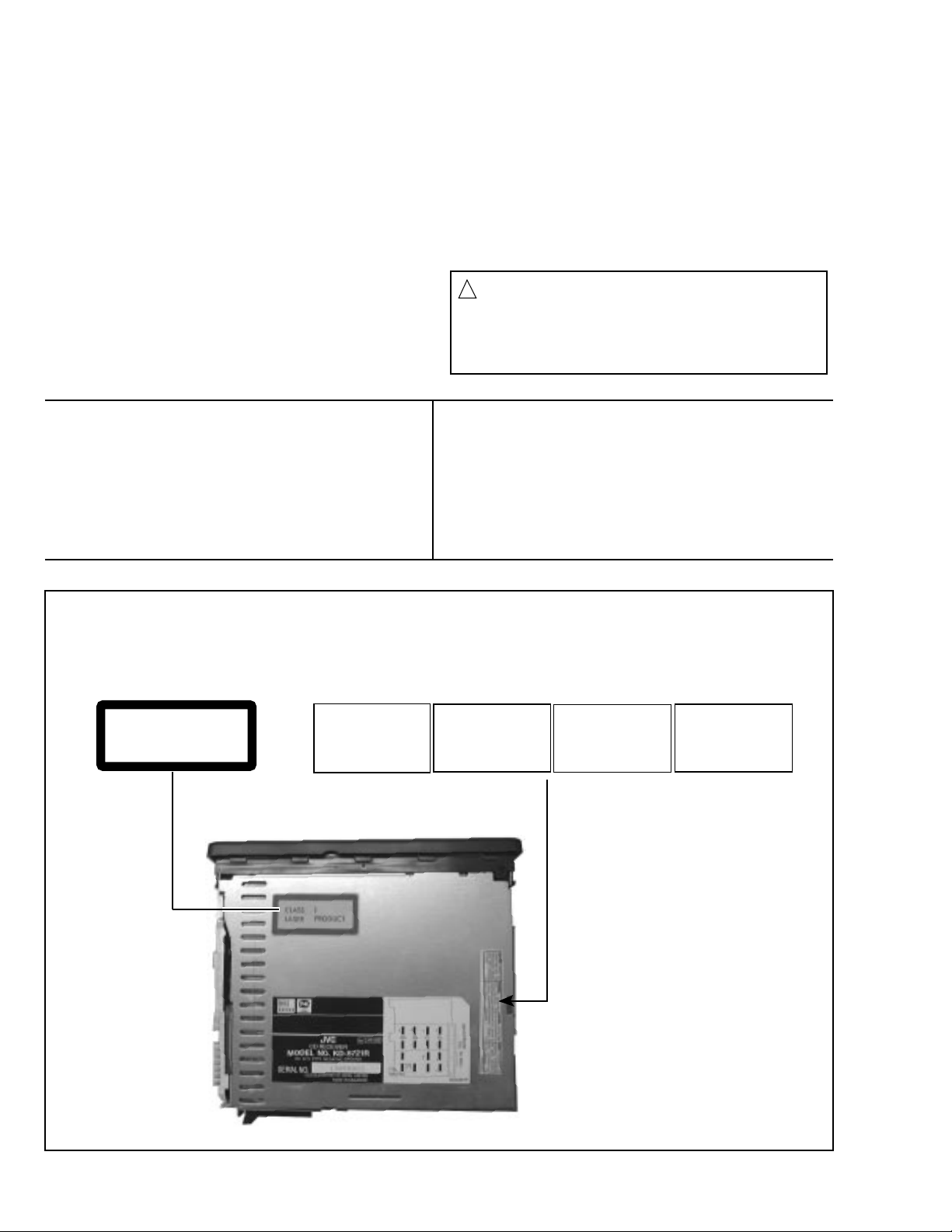
Important for laser products
1.CLASS 1 LASER PRODUCT
2.DANGER : Invisible laser radiation when open and inter
lock failed or defeated. Avoid direct exposure to beam.
3.CAUTION : There are no serviceable parts inside the
Laser Unit. Do not disassemble the Laser Unit. Replace
the complete Laser Unit if it malfunctions.
4.CAUTION : The compact disc player uses invisible
laserradiation and is equipped with safety switches
whichprevent emission of radiation when the drawer is
open and the safety interlocks have failed or are de
feated. It is dangerous to defeat the safety switches.
VARNING : Osynlig laserstrålning är denna del är öppnad
och spårren är urkopplad. Betrakta ej strålen.
VARO : Avattaessa ja suojalukitus ohitettaessa olet
alttiina näkymättömälle lasersäteilylle.Älä katso
säteeseen.
5.CAUTION : If safety switches malfunction, the laser is able
to function.
6.CAUTION : Use of controls, adjustments or performance of
procedures other than those specified herein may result in
hazardous radiation exposure.
CAUTION
!
Please use enough caution not to
see the beam directly or touch it
in case of an adjustment or operation
check.
ADVARSEL : Usynlig laserstråling ved åbning , når
sikkerhedsafbrydere er ude af funktion. Undgå
udsættelse for stråling.
ADVARSEL : Usynlig laserstråling ved åpning,når
sikkerhetsbryteren er avslott. unngå utsettelse
for stråling.
REPRODUCTION AND POSITION OF LABELS
WARNING LABEL
CLASS 1
LASER PRODUCT
DANGER : Invisibie laser
radiation when open and
interlock or defeated.
AVOID DIRECT EXPOSURE
TO BEAM (e)
ADVARSEL :Usynlig laserstråling ved åbning , når
sikkerhedsafbrydere er ude
af funktion. Undgå udsæt
telse for stråling. (f)
VARNING : Osynlig laserstrålning är denna del
är öppnad och spårren är
urkopplad. Betrakta ej
strålen. (s)
VARO : Avattaessa ja suojalukitus ohitettaessa olet
alttiina näkymättömälle
lasersäteilylle.Älä katso
säteeseen. (d)
1-4
Page 5
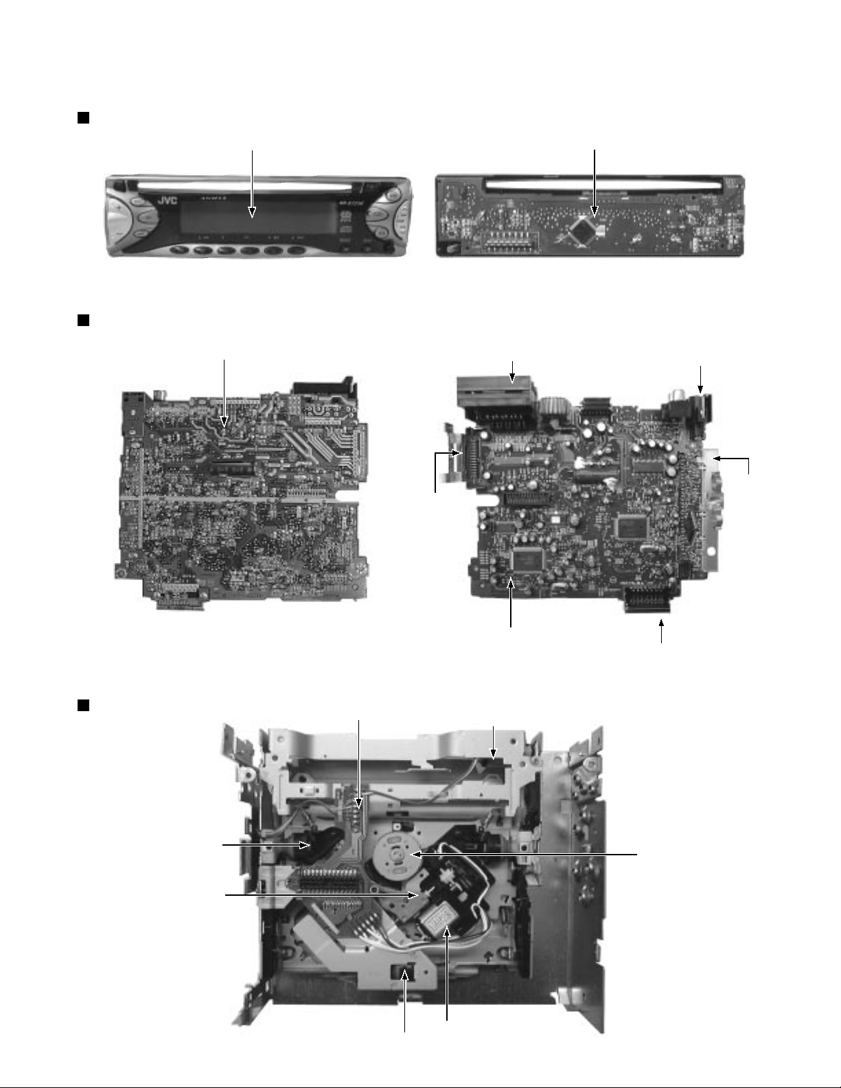
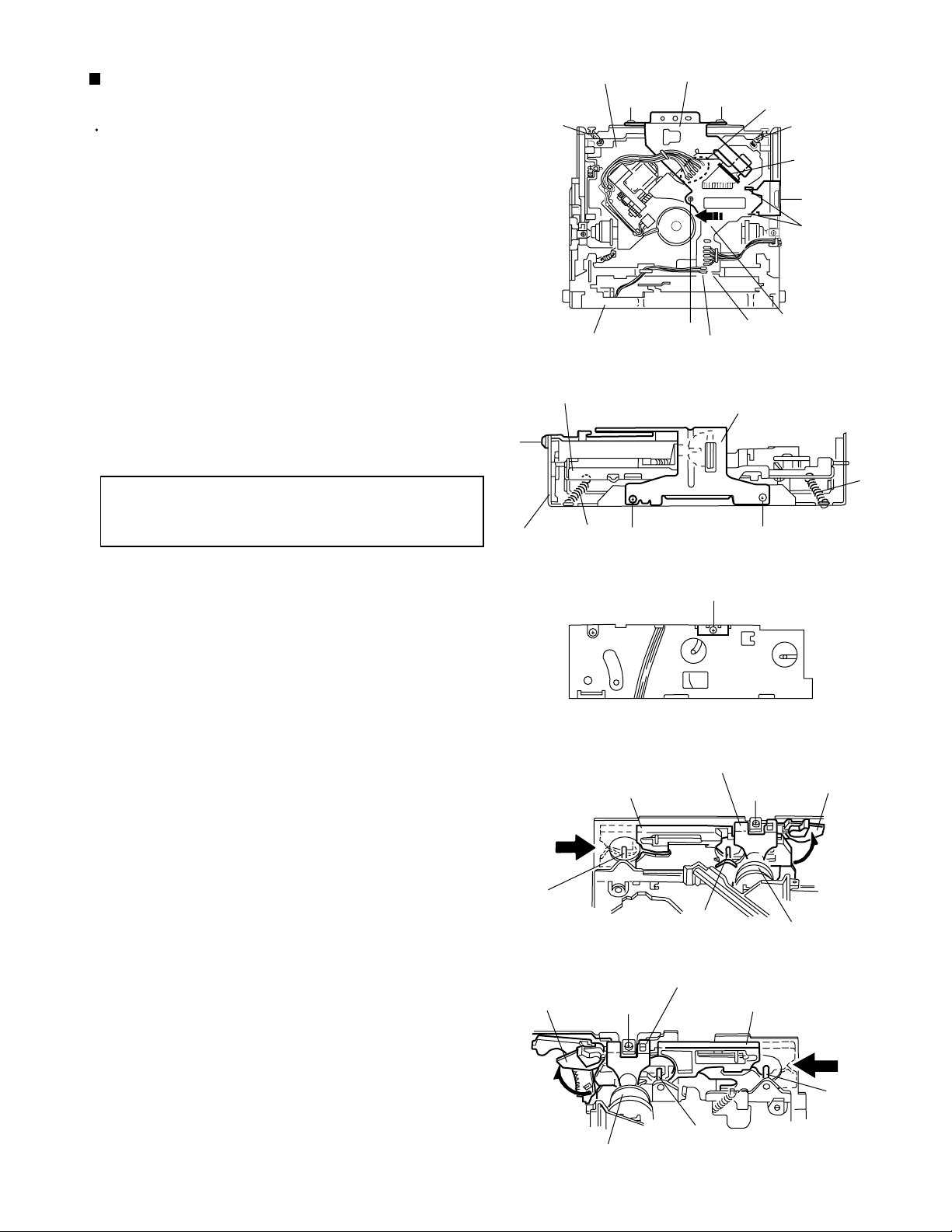
Location of main parts
Control unit
Display
Main unit
KD-S723R/KD-S721R
LED & key control board
Main board
CD mechanism
Power IC
Mechanism relay board
ISO connector
Main board
Loading motor
Antenna jack
Tuner
pack
Connector to controller
Damper
Pickup unit
Spindle motor
Feed motor
Damper
1-5
Page 6
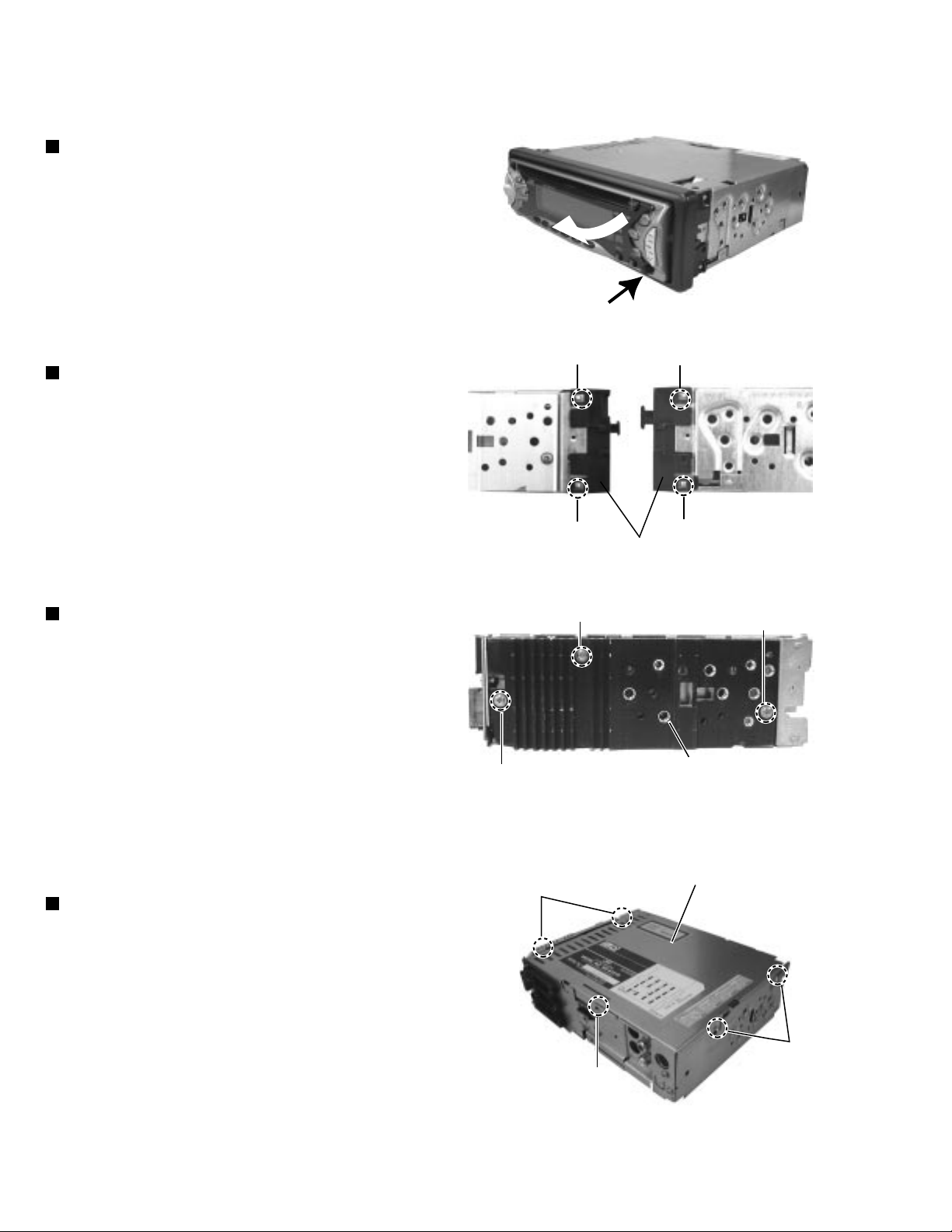
KD-S723R/KD-S721R
Disassembly method
Removing the front panel unit
(See Fig.1)
1. Press the release button and remove the front
panel unit in the direction of the arrow.
Fig.1
Removing the front chassis (See Fig.2)
1. Insert a screwdriver to the joints a on the side of the
front chassis and two joints b on the right side, then
detach the front chassis toward the front side.
Removing the heat sink (See Fig.3)
1. Remove the three screws A attaching the heat sink
on the left side of the body, and remove the heat
sink.
A
a
a
Front chassis
Fig.2
A
Fig. 3
b
b
A
Heat sink
Removing the bottom cover (See Fig.4)
1.2.Turn the body upside down.
Insert a screwdriver to the two joints c and two
joints d on both sides of the body and the joint e on
the back of the body, then detach the bottom cover
from the body.
1-6
Bottom cover
c
d
e
Fig. 4
Page 7
KD-S723R/KD-S721R
Removing the main amplifier board
(See Fig.5 and 6)
1.
Remove the front chassis.
2.
Remove the bottom cover.
3.
Remove the two screws B attaching the main
amplifier board assembly on the bottom of the body.
4.
Remove the three screws C attaching the main
amplifier board assembly on the back of the body.
5.
Disconnect connector CN501 on the main amplifier
board assembly from the CD mechanism assembly.
Main amplifier board
B
C
CN501
B
Fig.5
C
C
Fig. 6
Removing the CD mechanism assembly
(See Fig.7)
1.
Remove the front chassis.
2.
Remove the bottom cover.
3.
Remove the main amplifier board assembly.
4.
Remove the three screws D attaching the CD
mechanism assembly from the top cover.
Removing the control switch board
(See Fig.8 and 9)
1.
Remove the front chassis.
2.
Remove the four screws E attaching the rear cover
on the back of the front panel unit.
3.
Remove the control switch board from the front
panel unit.
CD mechanism assembly
Top cover
D
E
E
D
Fig. 7
E
Fig. 8
Control switch board
D
E
Fig. 9
1-7
Page 8
KD-S723R/KD-S721R
<CD mechanism section>
Removing the CD mechanism control
board (See Fig.1 and 2)
1.
Unsolder the part a and b on the CD mechanism
control board.
2.
Remove the stator fixing the CD mechanism control
board and the damper bracket (To remove the stator
smoothly, pick up the center part).
3.
Remove the screw A attaching the CD mechanism
control board.
4.
Remove the CD mechanism control board in the
direction of the arrow while releasing it from the two
damper bracket slots d and the front bracket slot e.
5.
Disconnect the flexible wire from connector on the
pickup unit.
ATTENTION:
Turn the FD gear in the direction of the
arrow to move the entire pickup unit to
the appropriate position where the
flexible wire of the CD mechanism unit
can be disconnected easily.
(Refer to Fig.2)
CD mechanism assembly
D
h
Front bracket
Pickup unit
Damper bracket
D
A
Fig.1
e
b
Flexible wire
a
h
c
D
d
CD mechanism
control board
Shift the lock
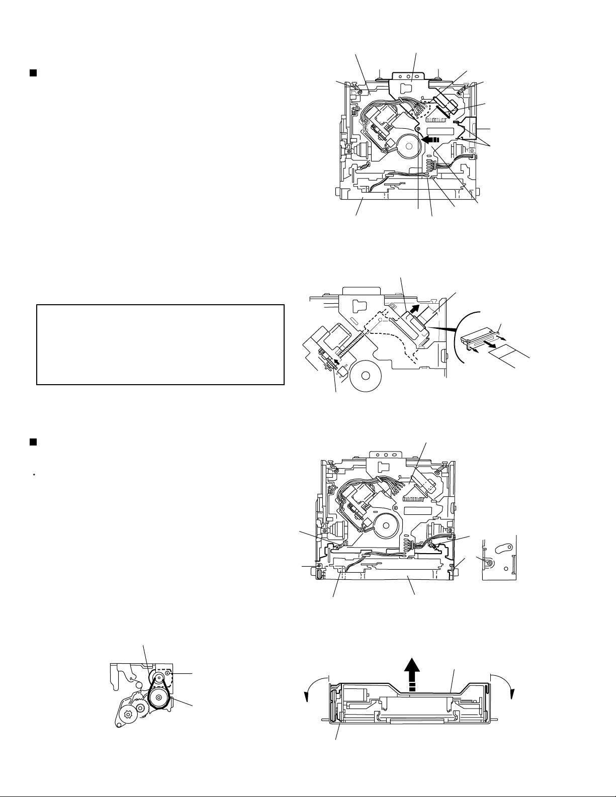
Removing the loading motor
(See Fig.3 to 5)
Prior to performing the following procedure, remove
the CD mechanism control board.
1.
Remove the two springs f attaching the CD
mechanism assembly and the front bracket.
2.
Remove the two screws B and the front bracket
while pulling the flame outward.
3.
Remove the belt and the screw C from the loading
motor.
Loading motor
C
FD gear
f
B
Loading motor
Pull outward
Fig.2
CD mechanism control board
f
B
Front bracket
Fig.3
Front bracket
Pull outward
1-8
Fig.5
Belt
Flame
Fig.4
Page 9
KD-S723R/KD-S721R
Removing the CD mechanism assembly
(See Fig.1, 6 to 9)
Prior to performing the following procedure, remove
the CD mechanism control board and the front
bracket (loading motor).
1.
Remove the three screws D and the damper
bracket.
2.
Raise the both sides fix arms and move the fix plates
in the direction of the arrow to place the four shafts g
as shown in Fig.8 and 9.
3.
Remove the CD mechanism assembly and the two
springs h attaching the flame.
4.
Remove the two screws E and both sides rear
damper brackets from the dampers. Detach the CD
mechanism assembly from the left side to the right
side.
ATTENTION:
The CD mechanism assembly can be
removed if only the rear damper
bracket on the left side is removed.
CD mechanism
h
Front bracket
CD mechanism
D
Flame
assembly
D
assembly
h
D
Damper bracket
D
A
Fig.5
e
b
Damper bracket
D
Fig.6
a
h
c
D
d
CD mechanism
control board
h
Fix plate (L)
g
Fix arm (R)
D
Fig.7
Rear damper bracket
g
Fig.8
Rear damper bracket
E
Fix plate(R)
E
Fix arm (L)
Damper
Damper
g
g
Fig.9
1-9
Page 10

KD-S723R/KD-S721R
Removing the feed motor assembly
(See Fig.10)
Prior to performing the following procedure, remove
the CD mechanism control board, the front bracket
(loading motor) and the CD mechanism assembly.
1.
Remove the two screws F and the feed motor
assembly.
Removing the pickup unit
(See Fig.10 and 11)
Prior to performing the following procedure, remove
the CD mechanism control board, the front bracket
(loading motor), the CD mechanism assembly and
the feed motor assembly.
1.
Detach the FD gear part of the pickup unit upward.
Then remove the pickup unit while pulling out the
part i of the FD screw.
Feed motor assembly
F
FD gear
Nut push spring plate
FD screw
Pickup unit
Fig.10
Part i
Part j
Pickup unit
G
Pickup mount nut
Pickup unit
ATTENTION:
2.
Remove the screw G attaching the nut push spring
plate and the pickup mount nut from the pickup unit.
Pull out the FD screw.
When reattaching the pickup unit,
reattach the part j of the pickup unit,
then the part i of the FD screw.
Removing the spindle motor
(See Fig.12 and 13)
Prior to performing the following procedure, remove
the CD mechanism control board, the front bracket
(loading motor), the CD mechanism assembly and
the feed motor assembly.
1.
Turn up the CD mechanism assembly and remove
the two springs k on both sides of the clamper arms.
Open the clamper arm upward.
2.
Turn the turn table, and remove the two screws H
and the spindle motor.
k
FD screw
Spindle motor
Fig.11
k
Fig.12
H
1-10
H
Fig.13
Page 11

Adjustment method
KD-S723R/KD-S721R
Test instruments required for adjustment
1. Digital oscilloscope (100MHz)
2. AM Standard signal generator
3. FM Standard signal generator
4. Stereo modulator
5. Electric voltmeter
6. Digital tester
7. Tracking offset meter
8. Test Disc JVC :CTS-1000
9. Extension cable for check
EXTGS004-26P 1
Standard measuring conditions
Power supply voltage DC14.4V(10.5~16V)
Load impedance 4 (4 to 8 allowance)
Output Level Line out 2.0V / 20 k (Vol. MAX)
How to connect the extension cable for adjusting
Standard volume position
Balance and Bass &Treble volume : lndication"0"
Loudness : OFF
BBE : OFF
Frequency Band
FM 87.5MHz ~ 108.0MHz
MW 522kHz ~ 1620 kHz
LW 144kHz ~ 279kHz
Dummy load
Exclusive dummy load should be used for AM,and FM. For
FM dummy load,there is a loss of 6dB between SSG output
and antenna input.The loss of 6dB need not be considered
since direct reading of figures are applied in this working
standard.
EXTGS004-26P
1-11
Page 12

KD-S723R/KD-S721R
Flow of functional operation until TOC read
Power ON
• When the pickup correctly moves
to the inner area of the disc
Set Function to CD
• When the laser diode correctly
emits
Microprocessor
commands
FMO
TC9462 "53"
FEED MOTOR
+TERMINAL
TERMINAL
IC501 "10"
REST SW
• When correctly focused
FEO
Focus Servo Loop ON
Disc inserted
Pickup feed to the inner area
Laser emitted
Focus search
Disc rotates
RF signal eye-pattern
remains closed
Tracking loop closed
RF signal eye-pattern
opens
TOC readout
YES
YES
Microprocessor
commands
1
"No disc"
display
• When the disc correctly rotates
Microprocessor
commands
Spindle
motor (-)
IC501 "7"
AccelerationAcceleration
0.5 Sec
Rough
Servo
0.5 Sec
Servo CLV
1-12
Jump to the first track
Play
Tracking Servo Loop ON
• RF signal
Rough Servo Mode
CLV Servo Mode
(ProgramArea)
CLV Servo Mode
(Lead-In Area;
Digital: 0)
Page 13

Feed Section
Is the voltage output at
IC541 pin "53" 5V or 0V?
YES
Is 4V present at both
sides of the feed motor?
YES
NO
Is the wiring for IC541
(90) ~ (100) correct?
NO
Is 6V or 2V present at
IC501 "10" and "11"?
NO
YES
YES
Is 5V present at IC501
pin "20"?
YES
Check the vicinity of
IC541.
Check the feed motor
connection wiring.
KD-S723R/KD-S721R
NONO
Check CD 9V
and 5V.
Check the feed motor.
Focus Section
When the lens is
moving:
4V
Does the S-search
waveform appear at
IC501 pins "6" and "7"?
Spindle Section
Is the disk rotated?
YES
Does the RF signal
appear at TP1?
YES
Is the RF waveform at TP1
distorted?
YES
Check IC501.
NO
YES
NO
NO
NO
Check the circuits in
the vicinity of IC501
pins "14" ~ "18".
Check the pickup and
its connections.
Is 4V present at IC501
pins "8" and "9" ?
Check the spindle motor
and its wiring.
Check the circuits in the
vicinity of IC521 "2" ~ "7",
"18"~"24" or the pickup
YES
YES
NO NO
Is 4V present at IC541
pin "55" ?
YES
Check the vicinity of
IC501.
Check IC521 and
IC541.
Proceed to the Tracking
section
Tracking Section
When the disc is rotated
at first:
Is the tracking error signal
output at IC521 "12"?
Check IC521.
Approx. 1.2 V
YES
Check the circuit in the
vicinity of IC521 pins
"2" ~ "12".
YESYES
Check the pickup and
its connections.
1-13
Page 14

KD-S723R/KD-S721R
Maintenance of laser pickup
(1) Cleaning the pick up lens
Before you replace the pick up, please try to
clean the lens with a alcohol soaked cotton
swab.
(2) Life of the laser diode
When the life of the laser diode has expired,
the following symptoms will appear.
(1) The level of RF output (EFM output:ampli
tude of eye pattern) will be low.
Is RF output
1.0 0.35Vp-p?
YES
O.K
(3) Semi-fixed resistor on the APC PC board
The semi-fixed resistor on the APC printed
circuit board which is attached to the pickup
is used to adjust the laser power.Since this
adjustment should be performed to match the
characteristics of the whole optical block,
do not touch the semi-fixed resistor.
If the laser power is lower than the specified
value,the laser diode is almost worn out, and
the laser pickup should be replaced.
If the semi-fixed resistor is adjusted while
the pickup is functioning normally,the laser
pickup may be damaged due to excessive current.
NO
Replace it.
Replacement of laser pickup
Turn off the power switch and,disconnect the
power cord from the ac outlet.
Replace the pickup with a normal one.(Refer
to "Pickup Removal" on the previous page)
Plug the power cord in,and turn the power on.
At this time,check that the laser emits for
about 3seconds and the objective lens moves
up and down.
Note: Do not observe the laser beam directly.
1-14
Play a disc.
Check the eye-pattern at TP1.
Finish.
Page 15

Description of major ICs
HA13164A(IC901):Regulator
1.Terminal layout
REMOTE
ANT
ACC.IN
VDD5V
SW5V
ACC5V
ANT.CTRL
MEMORY.IN
MEM.DET9VCTRL
123456789101112131415
2.Block diagram
CD8VAJILL10V
KD-S723R/KD-S721R
GND
3.Pin function
11
12
10
8
2
1
7
Surge Protector
BIAS TSD
15
3
TAB
note1) TAB (header of IC)
13
connected to GND
9
6
4
5
14
UNIT R:
C:F
Pin No. Symbol Function
1
2
REMOTE
ANT
Output voltage is VCC-1 V when M or H level applied to CTRL pin.
Output voltage is VCC-1 V when M or H level to CTRL pin and H level
to ANT-CTRL.
3
4
5
6
7
8
9
10
11
12
13
14
15
ACC.IN
VDD5V
SW5V
ACC5V
ANT.CTRL
MEMORY.IN
MEM.DET
9V
CTRL
CD8V
AJ
ILL10V
GND
Connected to ACC.
Regular 5.7V.
Output voltage is 5V when M or H level applied to CTRL pin.
Output for ACC detector.
L:ANT output OFF , H:ANT output ON
Connected to VCC.
Low battery detect.
Output voltage is 9V when M or H level applied to CTRL pin.
L:BIAS OFF, M:BIAS ON, H:CD ON
Output voltage is 8V when H level applied to CTRL pin.
Adjustment pin for ILM output voltage.
Output voltage is 10V when M or H level applied to CTRL pin.
Connected to GND.
1-15
Page 16

KD-S723R/KD-S721R
UPD178078GF-561 (IC701) : System CPU
81
~
NC
BUSINT
BUSSI
BUSSO
JBUS-SCK
NC
I2CDAI
I2CDAO
I2CCLK
NC
LCDDA
LCDSCK
BUSI/O
NC
LCDCE
SW2
SW3
SW4
RSTSW
NC
KEY0
KEY1
KEY2
LEVEL
AVDD
SM
SQ
NC
AVSS
REGCPU
VDD
REGOSC
X2
X1
GND0
SD/ST
GND2
NC
IFC
VDDPLL
OSC
NC
80 ~ 51
50
~
31
1 ~ 30
1.Pin layout
100
2.Pin function (1/2)
Pin
NO.
1
2
3
4
5
6,7
8
9
10
11
12
13
14
15
16
17
18
19
20
21,22
23
24
25
26
27
28
29
30,31
32
33
34
35
36
37
38
39
40
41
42
43
44
45
I/OSymbol FUNCTION
-
No connection
I
JVC bus communication line
I
JVC bus communication line
O
JVC bus communication line
O
JVC bus communication line
-
No connection
I
Serial data input
O
Serial data output
O
Serial clock output
-
No connection
O
LCD driver serial data output
O
LCD driver serial clock output
O
JVC bus output select
-
No connection
O
LCD driver communication line
I
CD mech switch
I
CD mech switch
I
CD mech switch
I
Traverse mech rest switch
I
No connection
I
Key input
I
Key input
I
Key input
I
Audio level input
-
Power supply
I
Signal level meter input
I
Signal quality input
-
Non connection
-
Connect to GND
-
Connect to GND with capacitor
-
Power supply
-
Connect to GND with capacitor
-
System clock
I
System clock
-
Connect to GND
I
Station detector & Stereo indicator
-
Connect to GND
-
No connection
I
IF count input
-
---
I
FM,AM osc input
-
No connection
1-16
Page 17

KD-S723R/KD-S721R
2.Pin function (2/2)
Pin
NO.
46
GNDPLL
47
AMEQ
48
FMEQ
49
IC(VPP)
50
RESET
51
SW1
52
REMOCON
53
NC
54
TEL_MUTE
55
POWER
56
CDON
57
MUTE
58
STAGE 1
59
BUZZER
60
STAGE 2
61~68
89~98
100
69
70
71
72
73
74
75
76
77
78
79
80
81
82
83
84
85
86
87
88
99
NC
LM0
LM1
BUCK
CCE
BUS0
BUS1
BUS2
BUS3
RST
PS1
PS2
DETACH
RDSSCK
GND1
MONO
SEEK/STOP
FM/AM
AFCK
RDSDATA
PLLMONITOR
NC
VDDPORT
GNDPORT
I/OSymbol FUNCTION
-
---
O
PLL error output for AM
O
PLL error output for FM
-
Setting to write for flash
I
System reset
I
CD mech switch
I
Remocon input
-
Non connection
O
TEL mute output
O
Power control
O
CD power control
O
Mute control
-
---
-
Non connection
-
---
-
Non connection
O
CD mech driver control
O
CD mech driver control
O
CD LSI communication line
O
CD LSI communication line
I/O
I/O
I/O
I/O
CD LSI communication line
CD LSI communication line
CD LSI communication line
CD LSI communication line
O
CD LSI communication line
I
ACC detection input
I
Memory detection
I
Detach detection
I
Clock input for RDS
-
Connect to GND
O
Mono by force
O
Switching SEEK & STOP
O
Band switch
O
AFcheck output
I
RDS data input
-
Non connection
-
Non connection
-
Vdd
-
Connect to GND
UPD178078GF-561
1-17
Page 18

KD-S723R/KD-S721R
LA4743K(IC302):Power AMP
1.Block diagram
+
0.22 F
+
0.22 F
11
1
12
6 20
-
+
Protective
circuit
-
+
2200 F 0.022 F
+
+
9
-
7
8
+
5
3
2
47 F
+5V
ST ON
+
0.22 F
N.C
+
0.22 F
4
Stand by
Switch
22
17
19
Mute
+
3.3 F
Low Level
Mute ON
10
+
Ripple
Filter
Mute
circuit
+
15
-
+
-
25
13
14
Protective
circuit
-
+
+
-
18
21
23
1-18
22 F
Muting &
16
+
ON Time Control
Circuit
24
Page 19

2.Terminal layout
KD-S723R/KD-S721R
VREF
3.Pin function
1
2
3
4
5
6
7
8
9
10
11
12
13
14
15
16
17
18
19
20
21
22
23
24
25
SymbolPin No. Function
TAB
GND1
OUTRRSTBY
OUTRR+
VCC1/2
OUTFRGND2
OUTFR+
VREF
INRR
INFR
SGND
INFL
INRF
ONTIME
OUTFL+
GND3
OUTFLVCC3/4
OUTRL+
MUTE
OUTRLGND4
NC
Header of IC
Power GND
Outpur(-) for front Rch
Stand by input
Output (+) for front Rch
Power input
Output (-) for rear Rch
Power GND
Output (+) for rear Rch
Ripple filter
Rear Rch input
Front Rch input
Signal GND
Front Lch input
Rear Lch input
Power on time control
Output (+) for rear Lch
Power GND
Output (-) for rear Lch
Power input
Output (+) for front
Muting control input
Output (-) for front
Power GND
No connection
LA4743K
1-19
Page 20

KD-S723R/KD-S721R
LA6567H-X(IC501):CD DRIVER
1.Pin layout & blockdiagram
VCC2
V05-
V05+
V04+
V04-
V03+
V03-
FR
1
2
3
4
5
6
7
FR
CH 3,4,5
Power supply
CH5
CH4
CH3
Thermal shutdown
Output control
Level shiftLevel shiftLevel shiftLevel shift
Input
22K 11K
Signal system power supply
28
27
26
25
24
23
22
FR
REV
FWD
S-GND
VCONT
VIN4
VIN4G
VCC-S
FR
V02+
V02-
V01+
V01-
VCC1
VIN1
VIN1G
8
9
10
11
12
13
14
CH2
CH1
CH1,2
Power supply
11K
22K
5VREG(PNPTr
The outside putting)
22K
11K
22K
11K
21
20
19
18
17
16
15
VREF-IN
REG-OUT
REG-IN
VIN3G
VIN3
VIN2G
VIN2
1-20
Page 21

KD-S723R/KD-S721R
2. Pin function
Pin no. Symbol
1
2
3
4
5
6
7
8
9
10
11
12
13
14
15
16
17
18
19
20
21
22
23
24
25
26
27
VCC2
V05V05+
V04+
V04V03+
V03V02+
V02V01+
V01-
VCC1
VIN1
VIN1G
VIN2
VIN2G
VIN3
VIN3G
REG-IN
REG-OUT
VREF-IN
VCC-S
VIN4G
VIN4
VCONT
S-GND
FWD
LA6567H-X(2/2)
Function
CH3,4,5 Power supply( It is short with VCC1,VCC-S)
Loading output(-)
Loading terminal (+)
CH4 Output terminal(+)
CH4 Output terminal(-)
CH3 Output terminal(+)
CH3 Output terminal(-)
CH2 Output terminal(+)
CH2 Output terminal(-)
CH1 Output terminal(+)
CH1 Output terminal(-)
CH1,2(BTL) Power supply(It is short with VCC-S,VCC2)
CH1 Input terminal
CH1 Input terminal(For gain adjustment)
CH2 Input terminal
CH2 Input terminal(For gain adjustment)
CH3 Input terminal
CH3 Input terminal(For gain adjustment)
Regulator terminal(Outside putting PNP base)
Regulator terminal(Outside putting PNP collector)
Standard voltage input terminal
Signal system power supply(It is short with VCC1,VCC2)
CH4 Input terminal(For gain adjustment)
CH4 Input terminal
5CH(VLO) Output voltage set terminal
Signal system GND
5CH(VLO)Signal output switch terminal(FWD),Input of logic of loading part
28
REV
5CH(VLO)Signal output switch terminal(REV),
Input of logic of loading part
Frame(FR)at the center becomes system GND.
Please be short-circuited on the outside and use the terminal of the power supply system
and three teminals of VCC-S, VCC1,VCC2.
1-21
Page 22

KD-S723R/KD-S721R
TC9462F(IC541):DSP&DAC
1.Pin layout & Block Diagram
81
82
83
84
85
86
87
88
89
90
91
92
93
94
95
96
97
98
99
100
80
79
LPF
1 2 3
78
Micon
interface
77
4 5
75
76
74
73
1bit
DAC
Clock
generator
Correction
circuit
Audio out
circuit
6
7 8 9 10 11 12 13
72
71 67
70
Address circuit
16KRAM
Digital out
69
68
66
65
64
ROM
Automatic adjustment
RAM
Synchronous
guarantee
EFM decode
Sub code
decoder
14 15
16 17 18 19 20 21 22
61 60
63
62
Servo
control
Digital equalizer
circuit
CLV servo
Status
58 57 56 55
59
PWM D/A
23 24 25
A/D
VCO
PLL
TMAX
54
Data
slicer
26
27 28 29 30
53 52 51
+
-
+
+
-
+
-
50
49
48
47
46
45
44
43
42
41
40
39
38
37
36
35
34
33
32
31
2.Pin function
PIN No.
1
2
3
4
5
6
7
8
9
10
11
12
13
14
15
16
17
18
19
20
21
22
23
24
25 P2V
SYMBOL
TEST0
HSO
UHSO
EMPH
LRCKOO
V
SS
BCK
AOUT
DOUT
MBOV
IPF
SBOK
CLCK
V
DD
V
SS
DATA
SFSY
SBSY
SPCK
SPDA
COFS
MONIT
V
DD
TESIO0--I
REF
FUNCTIONAL DESCRIPTION
I/O
Test mode terminal.Normally, Keep at open.
I
Playback speed mode flag output terminal.
UHSO
HSO
O
H
H
L
O
Subcode Q data emphasis flag output terminal.Emphasis ON at "H" level and OFF at "L"
level.The output polarity can invert by command.
Channel clock output terminal.(44.1khz)L-ch at "L" level and R-ch at "H" level. the output
polarity can invert by command.
Digital GND terminal.
--
O
Bit clock output terminal.(1.4112MHz)
Audio data output terminal.
O
Digital data output terminal.
O
Buffer memory over signal output terminal. Over at "H" level.
O
Correction flag output terminal. At "H" level,AOUT output is made to correction
O
impossibility by C
Subcode Q data CRCC check adjusting result output terminal.
O
The adjusting result is OK at "H" level.
Subcode P W data readout clock input/output terminal.
I/O
This terminal can select by command bit.
--
Digital power supply voltage terminal.
--
Digital GND terminal.
O
Subcode P W data output terminal.
O
Play-back frame sync signal output terminal.
O
Subcode block sync signal output terminal.
O
Processor status signal readout clock output terminal.
O
Processor status signal output terminal.
O
Correction frame clock output terminal. (7.35kHz)
Internal signal (DSP internal flag and PLL clock) output terminal.Selected by command.
O
This terminal output the text data with serial by command.
L
2
PLAYBACK SPEED
H
L
H
L
Nomal
2 times
4 times
--
correction processing.
Digital power supply voltage terminal.
Test input/output terminal.Normally,keep at "L" level.
The terminal that inputted the clock for read of text data by command.
--
PLL double reference voltage supply terminal.
REMARKS
With pull-up resistor.
--
--
--
--
--
--
--
--
--
--
--
--
--
--
--
--
--
--
--
--
--
--
--
1-22
Page 23

Pin No.
26
27
28
29
30
Symbol
HSSW
ZDET
PDO
TMAXS
TMAX
I/O
2/4 times speed at "VREF" voltage.
O
1 bit DA converter zero detect flag output terminal.
O
Phase difference signal output terminal of EFM
O
Function Remarks
signal and PLCK signal.
TMAX detection result output terminal. Selected by
O
command bit (TMPS)
TMAX detection result output terminal. Selected by
O
command bit (TMPS)
DIFFERENCE RESULT TMAX OUTPUT
Longer than fixed freq. "P2VREF"
Shorter than fixed freq. "VSS"
Within the fixed freq. "Hiz"
KD-S723R/KD-S721R
TC9462F(2/3)
2-state output(PVREF,HiZ)
3-state output.
(P2VREF,PVREF,VSS)
3-state output.
(P2VREF,PVREF,VSS)
3-state output.
(P2VREF,HiZ,VSS)
-
31
32
33
34
35
36
37
38
39
40
41
42
43
44
45
46
47
48
49
50
51
52
53
54
55
56
57
58~61
62
63
64~67
68
69
70
LPFN
LPFO
PVREF
VCOREF
VCOF
AVSS
SLCO
RFI
AVDD
RFCT
RFZI
RFRP
FEI
SBAD
TSIN
TEI
TEZI
FOO
TRO
VREF
RFGC
TEBC
FMO
FVO
DMO
2VREF
SEL
FLGA~D
VDD
VSS
IO0~3
DMOUT
CKSE
DDACT
LPF amplifier inverting terminal for PLL.
I
LPF amplifier output terminal for PLL.
O
PLL reference voltage supply terminal.
VCO center frequency reference level terminal. Normally,
I
keep at "PVREF" level.
VCO filter terminal.
O
Analog GND terminal.
Data slice level output terminal.
O
RF signal input terminal.
I
Analog power supply voltage terminal.
RFRP signal center level input terminal
I
RFRP zero cross input terminal
I
RF ripple signal input terminal
I
Focus error signal input terminal
I
Sub-beam adder signal input terminal
I
Test input terminal Normally, keep at "vref" level
I
Tracking error signal input terminal. Take in at tracking
I
servo ON.
Tracking error zero cross input terminal
I
Focus servo equalizer output terminal
O
Tracking servo equalizer output terminal
O
Analog reference voltage supply terminal
RF amplitude adjustment control signal output terminal
O
Tracking balance control signal output terminal
O
Feed equalizer output terminal
O
Speed error signal or feed search equalizer output
O
terminal
Disk equalizer output terminal
O
DSP, Synchronize to PXO)
Analog double reference voltage supply terminal
APC circuit ON/OFF indication signal output terminal
O
External flag output terminal for internal signal
O
Digital power supply voltage terminal
Digital GND terminal
General I/O terminal
I/O
This terminal control IO0~IO3 terminal
I
Normally, keep at open
I
DAC test mode terminal. Normally, keep at open
I
(PWM carrier=88.2kHz for
Analog input.
Analog output.
-
-
Analog output.
Analog output.
Analog input.
(Zin:selected by command)
Analog input(Zin : 50k )
Analog input.
Analog input.
Analog input.
Analog input.
Analog input.
Analog input.
Analog input(Zin :10k )
Analog output.(2VREF AVSS)
3-state PWM signal
output.
(2VREF,VREF,VSS)
(PWM carrier
=88.2kHz)
3-state output.
(2VREF,VREF,VSS)
-
-
-
-
-
With pull-up resistor.
With pull-up resistor.
With pull-up resistor.
1-23
Page 24

KD-S723R/KD-S721R
Pin No.
71
72
73
74
75
76
77
78
79
80
81
82
83
84
85
86
87~89
90~93
94
95
96
97
98
99
100
Symbol
TESIN
TESIO1
VSS
PXI
PXO
VDD
XVSS
XI
XO
XVDD
DVSR
RO
DVDD
DVR
LO
DVSL
TEST1~3
BUS0~3
VDD
VSS
BUCK
CCE
TEST4
TSMOD
RST
I/O
Test input terminal, Normally, keep at "L" level
I
Test input/output terminal. Normally, keep at "L" level
I
Digital GND terminal
Crystal oscillator connecting input terminal for DSP
I
Crystal oscillator connecting output terminal for DSP
O
Digital power supply voltage terminal
Oscillator GND terminal for system clock
Crystal oscillator connecting input terminal for system
I
clock
Crystal oscillator connecting output terminal for system
O
clock
Oscillator power supply voltage terminal for system clock
Analog GND terminal for DA converter (Rch)
R channel data forward output terminal
O
Analog supply voltage terminal for DA converter
Reference voltage terminal for DA converter
L channel data forward output terminal
O
Analog GND terminal for DA converter (Lch)
Test mode terminal . Normal keep at open
I
Micon interface data input/output terminal
I/O
Digital power supply voltage terminal
Digital GND terminal
Micon interface clock input terminal
I
Command and data sending/receiving chip enable signal
I
input terminal
Test mode terminal. Normal, keep at open
I
Local test mode selection terminal
I
Reset signal input terminal. Reset at "L" level
I
Function Remarks
TC9462F(3/3)
Analog input.
Analog input.
-
-
-
-
-
-
-
-
-
-
-
-
-
With piull-up resistor.
Schmit input.
With pull-up resistor.
-
Schmit input.
Schmit input.
With pull-up resistor.
With pull-up resistor.
With pull-up resistor.
1-24
Page 25

SAA6579T-X(IC71):RDS Detector
1.Pin layout
CLK
16
T57
15
OSCO
14
OSCI
13
V
dd
12
GND
11
TEST
10
MODE
9
SCOUT
2.Block diagram
QUAL
DATA
Vref
MUX
GND
CIN
1
2
3
4
dd
V
5
6
7
8
KD-S723R/KD-S721R
121413
3.Pin function
4
8
7
CLOCKED
COMPARATOR
5
3
REFERENCE
VOLT AGE
Pin No.
1
2
3
4
ANTIALIASING
FILTER
6 11
Symbol
QUAL
DATA
Vref
MUX
VP1
57 kHz
BANDPASS
(8th ORDER)
COSTAS LOOP
VARIABLE AND
FIXED DIVIDER
CLOCK
REGERATION
AND SYNC
Quality indication output
RDS data output
Reference voltage output (0.5VDDA)
Multiolex signal input
RECONSTRUCTION
FILTER
TEST LOGIC AND OUTPUT
SELECTOR SWITCH
Description
OSCILATOR
AND
DIVIDER
BIPHASE
SYMBOL
DECODER
910
QUALITY BIT
GENERATOR
DIFFERENTIAL
DECODER
1
2
15
15
5
6
7
8
9
10
11
12
13
14
15
16
Vdd
GND
CIN
SCOUT
MODE
TEST
GND
Vdd
OSCI
OSCO
T57
CLK
+5V supply voltage for analog part
Ground for analog part (0V)
Subcarrier input to comparator
Subcarrier output of reconstruction filter
Oscllator mode / test control input
Test enable input
Ground for digital part (0V)
+5V supply voltage for digital part
Oscillator input
Oscillator output
57 kHz clock signal output
RDS clock output
1-25
Page 26

KD-S723R/KD-S721R
TA2109F-X (IC501) : RF amp.
1. Pin layout
24 13
112
2. Block diagram
SBAD
13
FEO
14
10pF
FEN
15
VRO
16
RFRP
17
RFIS
18
RFGO
19
10k ohm
21k ohm
20k ohm
20k ohm
50k ohm
36pF
7.96k ohm
50uA
20k ohm
15k ohm 30k ohm
15k ohm
20uA
10k ohm
21k ohm
12k ohm
12k ohm
PEAK
BOTTOM
10k ohm
10k ohm
30k ohm
21k ohm 29k ohm
24k ohm 24k ohm
1.74k ohm
180k ohm
20pF
65uA
47k ohm
SW3
13k ohm
7.67k ohm
10k ohm
3 STATE
DET.
SW2
680 ohm
2.12k ohm
SW1
LDC
1k ohm
20pF
TEO
TEN
2VRO
TEB
SEL
LDO
MDI
12
11
10
9
8
7
6
3. Pin function
Pin
SymbolI/O
No.
Vcc
FNI
FPI
TPI
TNI
MDI
SEL
TEB
TEN
I
I
I
I
I
O
I
I
O
I
O
10
11
12
1
2
3
4
5
6
7
8
9
LDO
2VRO
TEO
RFGC
20
AGCI
21
re=130 ohm
RFO
22
GND
23
RFN
24
23.5k ohm
3.3k ohm
12k ohm
1.53k ohm
3.3k ohm
Pin function
Power supply input terminal
Main beam I-V amp input terminal
Main beam I-V amp input terminal
Sub beam I-v input terminal
Sub beam I-V input terminal
Monitor photo diode amp input terminal
Laser diode amp output terminal
Laser diode control signal input terminal
T. error balance adj. signal input terminal
Reference voltage output terminal
TE amp negative input terminal
TE error signal output terminal
180k ohm
40pF
180k ohm
Pin
No.
13
14
15
16
17
18
19
20
21
22
23
24
180k ohm
20pF
60k ohm
60k ohm
40pF
SymbolI/O
SBAD
RFRP
RFGO
RFGC
FEO
FEN
VRO
RFIS
AGCI
RFO
GND
RFN
O
O
I
O
O
I
O
I
I
O
-
I
TNI
TPI
FPI
FNI
Vcc
5
4
3
2
1
I-I
I-I
20k ohm
20k ohm
20k ohm
20k ohm
Pin function
Sub beam adder signal output terminal
Focus error signal output terminal
FE amp negative input terminal
Reference voltage (VREF) output terminal
Track count signal output terminal
RFRP detect circuit input terminal
RF gain signal output terminal
RF amplitude adj. control signal input terminal
RF signal amplitude adj. amp input terminal
RF signal output terminal
Ground terminal
RF amp negative input terminal
1-26
Page 27

LC75823W (IC601) : LCD driver
1. Pin Layout & Symbol
KD-S723R/KD-S721R
S1
S2
S3
S4
S5
S6
S7
S8
S9
S10
S11
S12
S13
S14
S15
S16
DICLCE
64 63 62 61 60 59 58 57 56 55 54 53 52 51 50 49
1
2
3
4
5
6
7
8
9
10
11
12
13
14
15
16
17 18 19 20 21 22 23 24 25 26 27 28 29 30 31 32
S17
S18
S19
OSC
S20
Vss
S21
VDD2
VDD1
S22
S23
INH
S24
VDD
S25
COM3
COM2
S26
S27
COM1
S52
S28
S29
S51
S30
S50
S31
S49
48
47
46
45
44
43
42
41
40
39
38
37
36
35
34
33
S32
S48
S47
S46
S45
S44
S43
S42
S41
S40
S39
S38
S37
S36
S35
S34
S33
2. Pin Function
Pin No.
1 to 52
53 to 55
COM1 to COM3
56
57
58
59
60
61
62
63
Symbol
S1 to S52
VDD
INH
VDD1
VDD2
Vss
OSC
CE
CL
I/O
O
Segment output pins used to display data transferred
Function
by serial data input.
O
Common driver output pins. The frame frequency is given
by : t0=(fosc/384)Hz.
--
Power supply connection. Provide a voltage of between
4.5 and 6.0V.
I
Display turning off input pin.
INT="L" (Vss) ----- off (S1 to S52, COM1 to COM3="L"
INT="H" (VDD)----- on
Serial data can be transferred in display off mode.
I
Used for applying the LCD drive 2/3 bias voltage
externally.
Must be connected to VDD2 when a 1/2 bias drive scheme
is used.
I
Used for applying the LCD drive 1/3 bias voltage
externally.
Must be connected to VDD1 when a 1/2 bias drive scheme
is used.
--
Power supply connection. Connect to GND.
I/O
Oscillator connection.
An oscillator circuit is formed by connecting an external
resistor and capacitor at this pin.
Serial data CE : Chip enable
interface connection
I
to the controller. CL : Sync clock
64
DI
DI : Transfer data
1-27
Page 28

KD-S723R/KD-S721R
TEA6320T-X (IC161) : E.volume
1.Pin layout
SDA
GND
OUTLR
OUTLF
TL
B2L
B1L
IVL
ILL
QSL
INCOCHL
IMO
INTUL
INCDL
1
2
3
4
5
6
7
8
9
10
11
12
13
14
15
16
32
31
30
29
28
27
26
25
24
23
22
21
20
19
18
17
SCL
VCC
OUTRR
OUTFR
TR
B2R
B1R
IVR
ILR
QSR
Vref
INCDCHR
CAP
INTUL
INCDR
2.Block diagram
10 8 9 7 6
21
31
2
19
16
15
13
11
14
22
20
18
17
POWER
SUPPLY
SOURCE
SELECTOR
23 25 24 26 27 28
VOLUME 1
+20 to -31 dB
LOUDNESS
LEFT
VOLUME 1
+20 to -31 dB
LOUDNESS
RIGHT
BASS
LEFT
+15 dB
LOGIC
BASS
RIGHT
+15 dB
5
TREBLE
LEFT
+12 dB
TREBLE
RIGHT
+12 dB
12
MUTE
FUNCTION
ZERO CROSS
DETECTOR
VOLUME 2
0 to 55 dB
BALANCE
FENDER REAR
VOLUME 2
0 to 55 dB
BALANCE
FENDER FRONT
HC BUS
REC
VOLUME 2
0 to -55dB
BALANCE
FENDER FRONT
VOLUME 2
0 to -55dB
BALANCE
FENDER REAR
3
4
32
1
29
30
3.Pin functions
Pin
Symbol
No.
SDA
1
GND
2
OUTLR
3
OUTLF
4
TL
5
B2L
6
B1L
7
IVL
8
ILL
9
QSL
10
11
12
I
NCDCHL
13
I/O
Serial data input/output.
I/O
Ground.
output left rear.
O
output left front.
O
Treble control capacitor left channel or
I
input from an external equalizer.
Bass control capacitor left channel or
-
output to an external equalizer.
Bass control capacitor left channel.
Input volume 1. left control part.
I
Input loudness. left control part.
I
Output source selector. left channel.
O
Not used
Not used
Input C left source.
I
Functions Functions
Pin
No.
17
18
19
20
21
22
23
24
25
26
27
28
29
Symbol
INCDR
INTUR
CAP
INCDCHR
Vref
QSR
ILR
IVR
B1R
B2R
TR
OUTRF
I/O
I
Input A right source.
I
Input B right source.
-
Electronic filtering for supply.
I
Input C right source.
-
Reference voltage (0.5Vcc)
-
Not used
O
Output source selector right channel.
I
Input loudness right channel.
I
Input volume 1. right control part.
-
Bass control capacitor right channel
Bass control capacitor right channel or
O
output to an external equalizer.
Treble control capacitor right channel or
I
input from an external equalizer.
O
Output right front.
1-28
14
15
16
IMO
INTUL
INCDL
Not used
Input B left source.
I
Input A left source.
I
30
31
32
OUTRR
Vcc
SCL
O
Output right rear.
-
Supply voltage.
I
Serial clock input.
Page 29

HD74HC126FP-X (IC801) : Buffer
KD-S723R/KD-S721R
1.Terminal layout
1C
1
1A
2
1Y
3
2C
4
2A
5
2Y
6
GND
7
2.Block diagram
Input
VU
14
4C
13
4A
12
4Y
11
3C
10
3A
9
3Y
8
Vcc Vcc
1A
2A
3A
4A
1C
2C
3C
See Function Table
4C
3.Pin function
Output
1Y
2Y
Output
2Y
Output
3Y
Output
4Y
Input
C
L
H
H
A
X
L
H
Output
Y
Z
H
L
Note) H:High level
L:Low level
X:Irrelevant
Z:Off(High-impedance)
State a 3-state input
1k
S1
CL
1k
Sample as Load Circuit 1
Sample as Load Circuit 1
Sample as Load Circuit 1
Note) CL includes probe and jig capacitance
NJM4565M-WE (IC581) : Ope. amp
A OUTPUT
-
A INPUT
+
A INPUT
1
2
3
-
4
V
+
8
V
B OUTPUT
7
-
B INPUT
6
5
+
B INPUT
1-29
Page 30

KD-S723R/KD-S721R
VICTOR COMPANY OF JAPAN, LIMITED
MOBILE ELECTRONICS DIVISION
PERSONAL & MOBILE NETWORK BUSINESS UNIT. 10-1,1Chome,Ohwatari-machi,Maebashi-city,371-8543,Japan
(No.49693)
200202
 Loading...