

Page 1
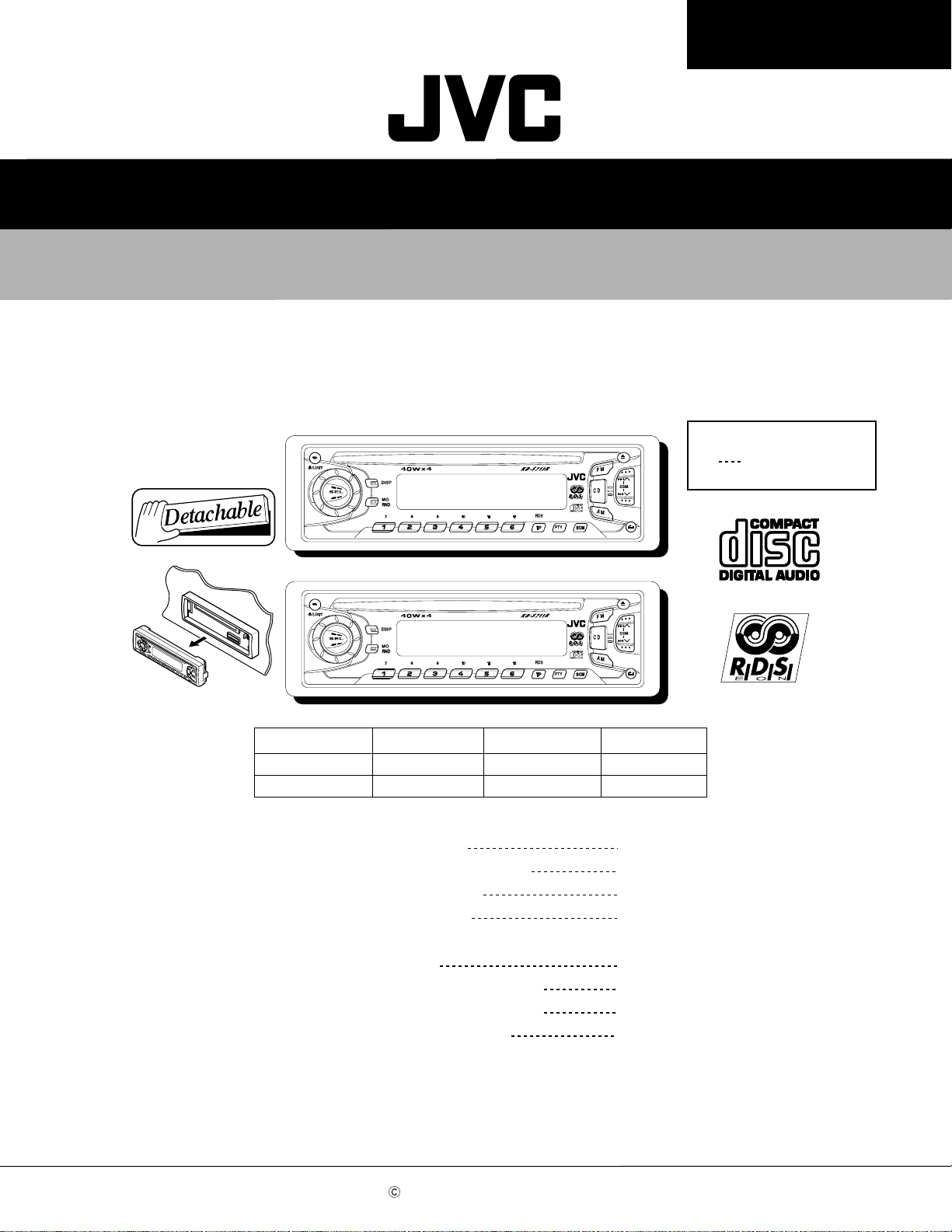
KD-S713R/KD-S711R
SERVICE MANUAL
CD RECEIVER
KD-S713R / KD-S711R
E Continental Europe
Area Suffix
Difference piont
KD-S713R
KD-S711R
Contents
Safety preccaution
Preventing static electricity
Disassembly method
Adjustment method
Flow of functional operation
until TOC read
Maintenance of laser pickup
Replacement of laser pickup
Description of major ICs
LCD back light
AMBER
GREEN
COPYRIGHT 2001 VICTOR COMPANY OF JAPAN, LTD.
Control buttons
AMBER
GREEN
SCM buttons
GREEN
RED
1-2
1-3
1-4
1-9
1-10
1-11
1-11
1-12~25
No.49603
Jun. 2001
Page 2
KD-S713R/KD-S711R
Safety precaution
!
!
Burrs formed during molding may be left over on some parts of the chassis. Therefore,
pay attention to such burrs in the case of preforming repair of this system.
Please use enough caution not to see the beam directly or touch it in case of an
adjustment or operation check.
1-2
Page 3
KD-S713R/KD-S711R
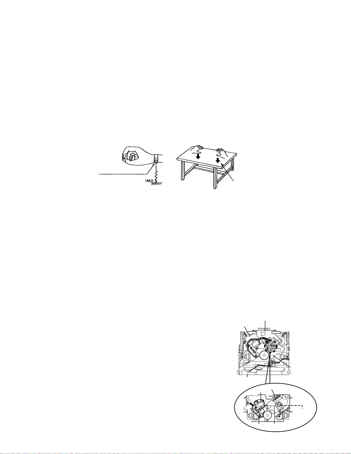
Preventing static electricity
1.Grounding to prevent damage by static electricity
Electrostatic discharge (ESD), which occurs when static electricity stored in the body, fabric, etc. is discharged,
can destroy the laser diode in the traverse unit (optical pickup). Take care to prevent this when performing repairs.
2.About the earth processing for the destruction prevention by static electricity
Static electricity in the work area can destroy the optical pickup (laser diode) in devices such as CD players.
Be careful to use proper grounding in the area where repairs are being performed.
2-1 Ground the workbench
Ground the workbench by laying conductive material (such as a conductive sheet) or an iron plate over
it before placing the traverse unit (optical pickup) on it.
2-2 Ground yourself
Use an anti-static wrist strap to release any static electricity built up in your body.
(caption)
Anti-static wrist strap
Conductive material
(conductive sheet) or iron plate
3. Handling the optical pickup
1. In order to maintain quality during transport and before installation, both sides of the laser diode on the
replacement optical pickup are shorted. After replacement, return the shorted parts to their original condition.
(Refer to the text.)
2. Do not use a tester to check the condition of the laser diode in the optical pickup. The tester's internal power
source can easily destroy the laser diode.
4.Handling the traverse unit (optical pickup)
1. Do not subject the traverse unit (optical pickup) to strong shocks, as it is a sensitive, complex unit.
2. Cut off the shorted part of the flexible cable using nippers, etc. after replacing the optical pickup. For specific
details, refer to the replacement procedure in the text. Remove the anti-static pin when replacing the traverse
unit. Be careful not to take too long a time when attaching it to the connector.
3. Handle the flexible cable carefully as it may break when subjected to strong force.
4. It is not possible to adjust the semi-fixed resistor that adjusts the laser power. Do not turn it
CD mechanism ass’y
Damper bracket
Attention when traverse unit is decomposed
*Please refer to "Disassembly method" in the text for pick-up and how to
detach the substrate.
1.Solder is put up before the card wire is removed from connector on
the CD substrate as shown in Figure.
(When the wire is removed without putting up solder, the CD pick-up
assembly might destroy.)
2.Please remove solder after connecting the card wire with
when you install picking up in the substrate.
Front bracket
Feed motor ass’y
FD screw
CD mechanism
control board
Soldering
FD gear
Pickup unit
1-3
Page 4
KD-S713R/KD-S711R
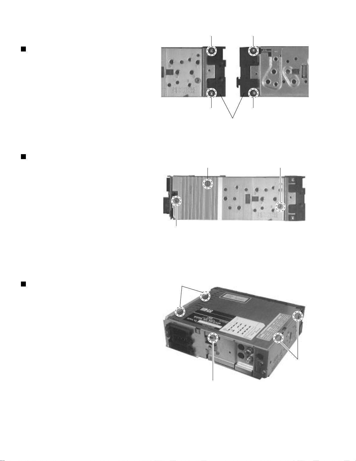
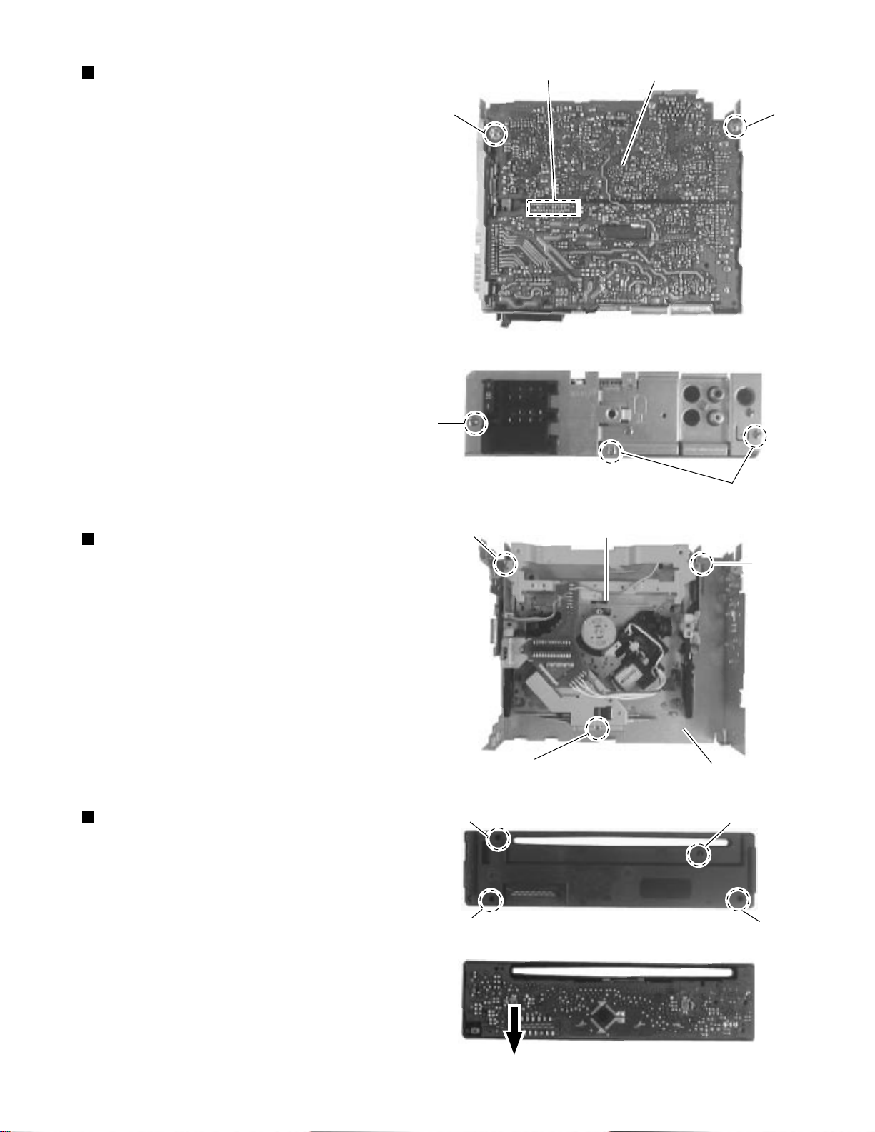
Disassembly method
Removing the front chassis (See Fig.1)
1.
Insert a screwdriver to the joints a on the side of
the front chassis and two joints b on the right
side, then detach the front chassis toward the
front side.
Removing the heat sink (See Fig.2)
1.
Remove the three screws A attaching the heat
sink on the left side of the body, and remove the
heat sink.
ab
ab
Front chassis
Fig. 1
A
A
Removing the bottom cover (See Fig.3)
1.
Turn the body upside down.
2.
Insert a screwdriver to the two joints c and two
joints d on the both sides of the body and the
joint e on the back of the body, then detach the
bottom cover from the body.
A
Fig. 2
c
d
e
Fig. 3
1-4
Page 5
KD-S713R/KD-S711R
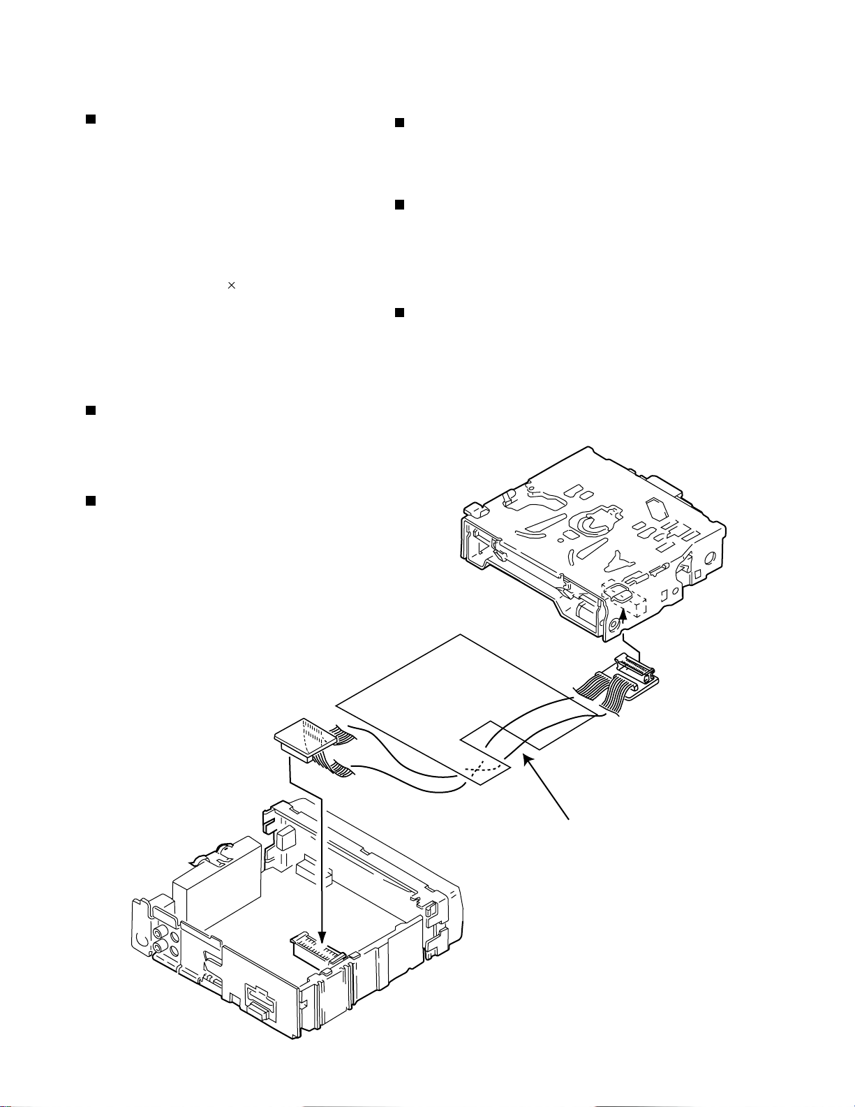
Removing the main board
(See Fig.4 and 5)
1.
Remove the front chassis.
2.
Remove the bottom cover.
3.
Remove the two screws B attaching the main
board on the bottom of the body.
4.
Remove the three screws C attaching the main
board on the back of the body.
5.
Disconnect the connector CN501 from the CD
mechanism assembly.
C
B
CN501 Main board
B
Fig. 4
Removing the CD mechanism assembly
(See Fig.6)
1.
Remove the front chassis.
2.
Remove the bottom cover.
3.
Remove the main board.
4.
Remove the three screws D attaching the CD
mechanism assembly from the top cover.
Removing the front board
(See Fig.7 and 8)
1.
Remove the front chassis.
2.
Remove the four screws E attaching the rear
cover on the back of the front panel unit.
3.
Remove the front board from the front panel unit.
D
Fig. 5
CD mechanism assembly
C
D
D
Fig. 6
Top cover
EE
EE
Fig. 7
Fig. 8
1-5
Page 6
KD-S713R/KD-S711R
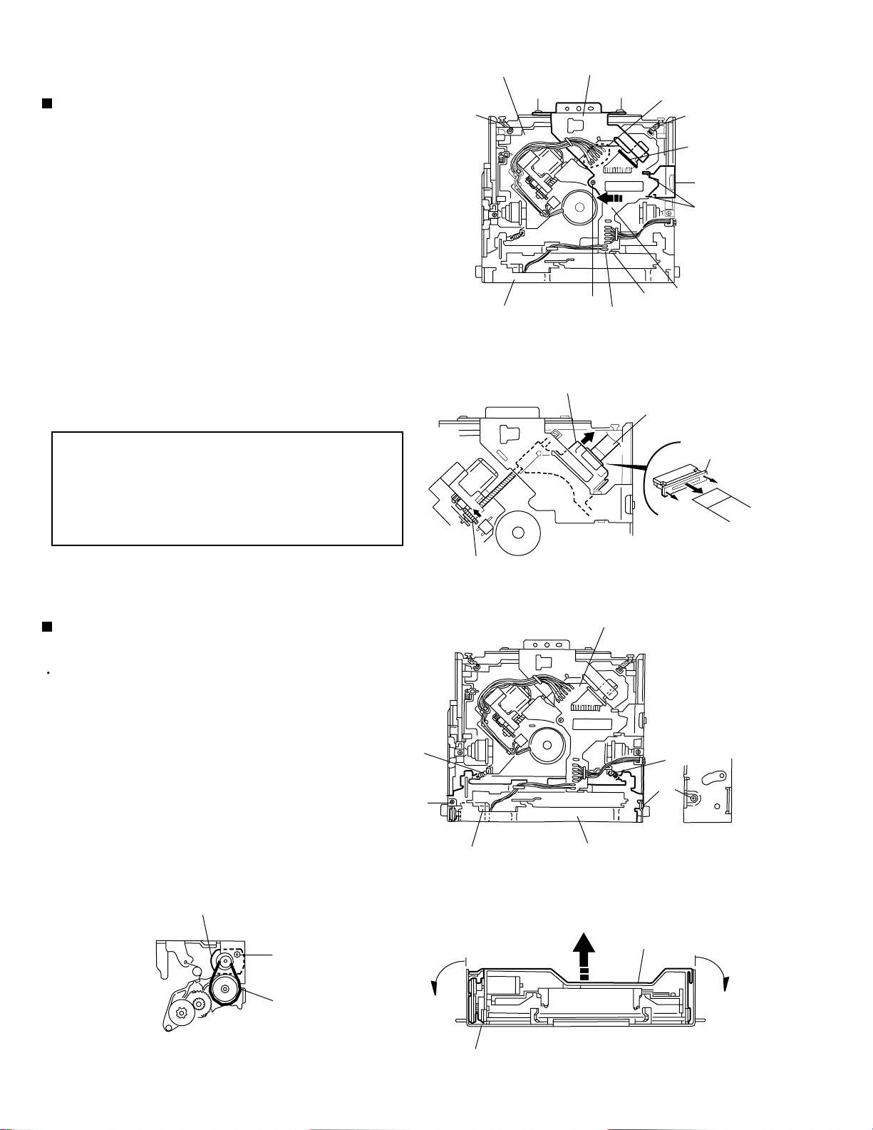
<CD mechanism section>
Removing the CD mechanism control
board (See Fig.1 and 2)
1.
Unsolder the part a and b on the CD mechanism
control board.
2.
Remove the stator fixing the CD mechanism control
board and the damper bracket (To remove the stator
smoothly, pick up the center part).
3.
Remove the screw A attaching the CD mechanism
control board.
4.
Remove the CD mechanism control board in the
direction of the arrow while releasing it from the two
damper bracket slots d and the front bracket slot e.
5.
Disconnect the flexible wire from connector on the
pickup unit.
ATTENTION:
Turn the FD gear in the direction of the
arrow to move the entire pickup unit to
the appropriate position where the
flexible wire of the CD mechanism unit
can be disconnected easily.
(Refer to Fig.2)
CD mechanism assembly
D
h
Front bracket
Pickup unit
Damper bracket
D
A
Fig.1
e
b
Flexible wire
a
h
c
D
d
CD mechanism
control board
Shift the lock
Removing the loading motor
(See Fig.3 to 5)
Prior to performing the following procedure, remove
the CD mechanism control board.
1.
Remove the two springs f attaching the CD
mechanism assembly and the front bracket.
2.
Remove the two screws B and the front bracket
while pulling the flame outward.
3.
Remove the belt and the screw C from the loading
motor.
Loading motor
C
FD gear
f
B
Loading motor
Pull outward
Fig.2
CD mechanism control board
f
B
Front bracket
Fig.3
Front bracket
Pull outward
1-6
Fig.5
Belt
Flame
Fig.4
Page 7

KD-S713R/KD-S711R
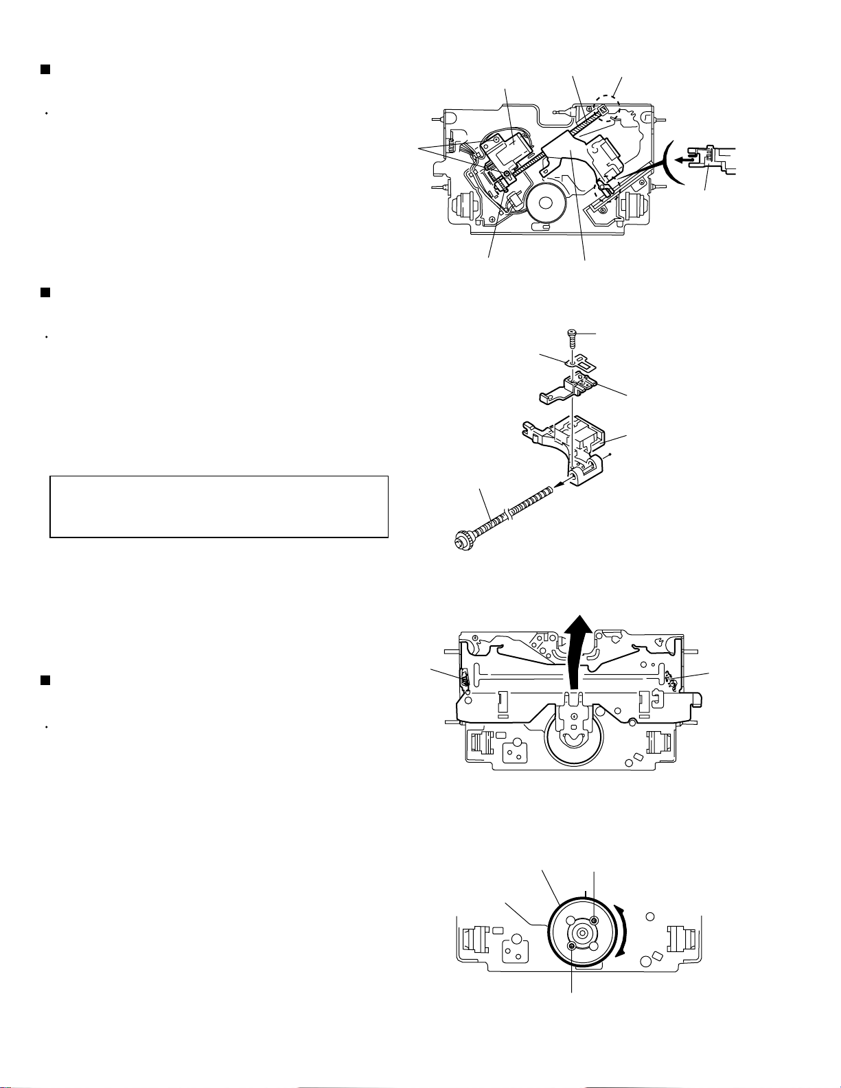
Removing the CD mechanism assembly
(See Fig.1, 6 to 9)
Prior to performing the following procedure, remove
the CD mechanism control board and the front
bracket (loading motor).
1.
Remove the three screws D and the damper
bracket.
2.
Raise the both sides fix arms and move the fix plates
in the direction of the arrow to place the four shafts g
as shown in Fig.8 and 9.
3.
Remove the CD mechanism assembly and the two
springs h attaching the flame.
4.
Remove the two screws E and both sides rear
damper brackets from the dampers. Detach the CD
mechanism assembly from the left side to the right
side.
ATTENTION:
The CD mechanism assembly can be
removed if only the rear damper
bracket on the left side is removed.
CD mechanism
h
Front bracket
CD mechanism
D
Flame
assembly
D
assembly
h
D
Damper bracket
D
A
Fig.1
e
b
Damper bracket
D
Fig.6
a
h
c
D
d
CD mechanism
control board
h
g
Fix arm (R)
Fix plate (L)
E
D
Fig.7
Rear damper bracket
E
g
Fig.8
Rear damper bracket
Fix plate(R)
Fix arm (L)
Damper
Damper
g
g
Fig.9
1-7
Page 8
KD-S713R/KD-S711R
Removing the feed motor assembly
(See Fig.10)
Prior to performing the following procedure, remove
the CD mechanism control board, the front bracket
(loading motor) and the CD mechanism assembly.
1.
Remove the two screws F and the feed motor
assembly.
Removing the pickup unit
(See Fig.10 and 11)
Prior to performing the following procedure, remove
the CD mechanism control board, the front bracket
(loading motor), the CD mechanism assembly and
the feed motor assembly.
1.
Detach the FD gear part of the pickup unit upward.
Then remove the pickup unit while pulling out the
part i of the FD screw.
Feed motor assembly
F
FD gear
Nut push spring plate
FD screw
Pickup unit
Fig.10
Part i
Part j
Pickup unit
G
Pickup mount nut
Pickup unit
ATTENTION:
2.
Remove the screw G attaching the nut push spring
plate and the pickup mount nut from the pickup unit.
Pull out the FD screw.
When reattaching the pickuap unit,
reattach the part j of the pickup unit,
then the part i of the FD screw.
Removing the spindle motor
(See Fig.12 and 13)
Prior to performing the following procedure, remove
the CD mechanism control board, the front bracket
(loading motor), the CD mechanism assembly and
the feed motor assembly.
1.
Turn up the CD mechanism assembly and remove
the two springs k on both sides of the clamper arms.
Open the clamper arm upward.
2.
Turn the turn table, and remove the two screws H
and the spindle motor.
k
FD screw
Spindle motor
Fig.11
k
Fig.12
H
1-8
H
Fig.13
Page 9
Adjustment method
KD-S713R/KD-S711R
Test instruments required for adjustment
1. Digital oscilloscope (100MHz)
2. AM Standard signal generator
3. FM Standard signal generator
4. Stereo modulator
5. Electric voltmeter
6. Digital tester
7. Tracking offset meter
8. Test Disc JVC :CTS-1000
9. Extension cable for check
EXTGS004-26P 1
Standard measuring conditions
Power supply voltage DC14.4V(10.5~16V)
Load impedance 20Kohm(2 Speakers connection)
Output Level Line out 2.0V (Vol. MAX)
How to connect the extension cable for adjusting
Standard volume position
Balance and Bass &Treble volume : lndication"0"
Loudness : OFF
BBE : OFF
Frequency Band
FM 87.5MHz ~ 108.0MHz
MW 144kHz ~ 279kHz, 520kHz ~ 1620 kHz
Dummy load
Exclusive dummy load should be used for AM,and FM. For
FM dummy load,there is a loss of 6dB between SSG output
and antenna input.The loss of 6dB need not be considered
since direct reading of figures are applied in this working
standard.
EXTGS004-26P
1-9
Page 10
KD-S713R/KD-S711R
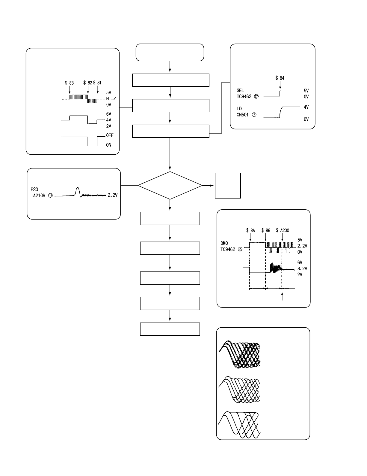
Flow of functional operation until TOC read
Power ON
• When the pickup correctly moves
to the inner area of the disc
Set Function to CD
• When the laser diode correctly
emits
Microprocessor
commands
FMO
TC9462 "53"
FEED MOTOR
+TERMINAL
TERMINAL
IC581 "5"
REST SW
• When correctly focused
Focus Servo Loop ON
Disc inserted
Pickup feed to the inner area
Laser emitted
Focus search
Disc rotates
RF signal eye-pattern
remains closed
Tracking loop closed
RF signal eye-pattern
opens
TOC readout
YES
YES
Microprocessor
commands
"No disc"
display
• When the disc correctly rotates
Microprocessor
commands
Spindle
motor (-)
IC581 "7"
AccelerationAcceleration
0.5 Sec
Rough
Servo
0.5 Sec
Servo CLV
1-10
Jump to the first track
Play
Tracking Servo Loop ON
• RF signal
Rough Servo Mode
CLV Servo Mode
(ProgramArea)
CLV Servo Mode
(Lead-In Area;
Digital: 0)
Page 11
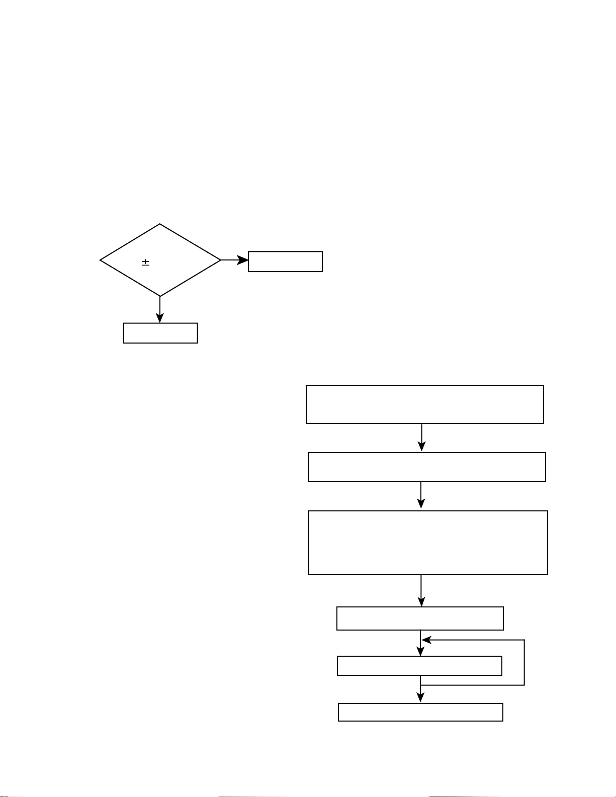
Maintenance of laser pickup
(1) Cleaning the pick up lens
Before you replace the pick up, please try to
clean the lens with a alcohol soaked cotton
swab.
(2) Life of the laser diode
When the life of the laser diode has expired,
the following symptoms will appear.
(1) The level of RF output (EFM output:ampli
tude of eye pattern) will be low.
KD-S713R/KD-S711R
Is RF output
1.0 0.35Vp-p?
YES
O.K
(3) Semi-fixed resistor on the APC PC board
The semi-fixed resistor on the APC printed
circuit board which is attached to the pickup
is used to adjust the laser power.Since this
adjustment should be performed to match the
characteristics of the whole optical block,
do not touch the semi-fixed resistor.
If the laser power is lower than the specified
value,the laser diode is almost worn out, and
the laser pickup should be replaced.
If the semi-fixed resistor is adjusted while
the pickup is functioning normally,the laser
pickup may be damaged due to excessive current.
NO
Replace it.
Replacement of laser pickup
Turn off the power switch and,disconnect the
power cord from the ac outlet.
Replace the pickup with a normal one.(Refer
to "Pickup Removal" on the previous page)
Plug the power cord in,and turn the power on.
At this time,check that the laser emits for
about 3seconds and the objective lens moves
up and down.
Note: Do not observe the laser beam directly.
Play a disc.
Check the eye-pattern at TP1.
Finish.
1-11
Page 12
KD-S713R/KD-S711R
Description of major ICs
UPD178078GF-540 (IC701) : System CPU
81
~
NC
BUSINT
BUSSI
BUSSO
JBUS-SCK
NC
I2CDAI
I2CDAO
I2CCLK
NC
LCDDA
LCDSCK
BUSI/O
NC
LCDCE
SW2
SW3
SW4
RSTSW
ENC1
ENC2
KEY0
KEY1
KEY2
LEVEL
AVDD
SM
SQ
NC
AVSS
REGCPU
VDD
REGOSC
X2
X1
GND0
SD/ST
GND2
NC
IFC
VDDPLL
OSC
NC
80 ~ 51
50
~
31
1 ~ 30
1.Pin layout
100
2.Pin function (1/2)
Pin
NO.
1
2
3
4
5
6,7
8
9
10
11
12
13
14
15
16
17
18
19
20
21
22
23
24
25
26
27
28
29
30,31
32
33
34
35
36
37
38
39
40
41
42
43
44
45
I/OSymbol FUNCTION
-
Non connection
I
JVC bus communication line
I
JVC bus communication line
O
JVC bus communication line
O
JVC bus communication line
-
Non connection
I
Serial data input
O
Serial data output
O
Serial clock output
-
Non connection
O
LCD driver serial data output
O
LCD driver serial clock output
O
JVC bus output select
-
Non connection
O
LCD driver communication line
I
CD mech switch
I
CD mech switch
I
CD mech switch
I
Traverse mech rest switch
I
Encoder input
I
Encoder input
I
Key input
I
Key input
I
Key input
I
Audio level input
-
Power supply
I
Signal level meter input
I
Signal quality input
-
Non connection
-
Connect to GND
-
Connect to GND with capacitor
-
Power supply
-
Connect to GND with capacitor
-
System clock
I
System clock
-
Connect to GND
I
Station detector & Stereo indicator
-
Connect to GND
-
Non connection
I
IF count input
-
---
I
FM,AM osc input
-
Non connection
1-12
Page 13
2.Pin function (2/2)
Pin
NO.
46
47
48
49
50
51
52
53
54
55
56
57
58
59
60
61~68
69
70
71
72
73
74
75
76
77
78
79
80
81
82
83
84
85
86
87
88
89~98
99
100
GNDPLL
AMEQ
FMEQ
IC(VPP)
RESET
SW1
REMOCON
NC
TEL_MUTE
POWER
CDON
MUTE
STAGE 1
BUZZER
STAGE 2
NC
LM0
LM1
BUCK
CCE
BUS0
BUS1
BUS2
BUS3
RST
PS1
PS2
DETACH
RDSSCK
GND1
MONO
SEEK/STOP
FM/AM
AFCK
RDSDATA
PLLMONITOR
NC
VDDPORT
GNDPORT
I/OSymbol FUNCTION
-
---
O
PLL error output for AM
O
PLL error output for FM
-
Setting to write for flash
I
System reset
I
CD mech switch
I
Remocon input
-
Non connection
O
TEL mute output
O
Power control
O
CD power control
O
Mute control
-
---
-
Non connection
-
---
-
Non connection
O
CD mech driver control
O
CD mech driver control
O
CD LSI communication line
O
CD LSI communication line
I/O
I/O
I/O
I/O
CD LSI communication line
CD LSI communication line
CD LSI communication line
CD LSI communication line
O
CD LSI communication line
I
ACC detection input
I
Memory detection
I
Detach detection
I
Clock input for RDS
-
Connect to GND
O
Mono by force
O
Switching SEEK & STOP
O
Band switch
O
AFcheck output
I
RDS data input
-
Non connection
-
Non connection
-
Vdd
-
Connect to GND
KD-S713R/KD-S711R
1-13
Page 14
KD-S713R/KD-S711R
BA4905-V3 (IC961) : Regulator
1.Terminal layout
1234 56 789101112
2.Block diagram
REGULATOR
EXT
OIVPC
RESET
1 2 3 4 5 6 7 8 9 10 11 12
RESET COMP VDD 5.7V CD 8V VCC AJ
EXT ACC AUDIO 9V CTRL ILM 10V GND
37K
5K
1-14
Page 15

KD-S713R/KD-S711R
Explanation of terminals
1
2
2
4
5
6
7
8
9
RESET
EXT output
COMP output
ACC
VDD output
AUDIO output
CD output
CTRL
VCC
BA4905-V3
If VDD voltage becomes 4V or less, RESET output becomes low level.
This outout voltage is approximately 0.5V lower than VCC, and max
output current is 300mA.
A voltage supply for ACC block this outout voltage is approximately
0.7V lower than VDD'S. The max output current is 100mA.
Control of the COMP output by inputting voltage.
This output voltage is 5.7V, and max output current is 100mA.
This voltage supply is for microcomputer. Whenever block up voltage
supply is connected. the output keeps on running.
This output voltage is 9.0V, and max output current is 500mA.
This voltage supply for AUDIO.
This output voltage is 8.0V, and max output current is 1A.
This voltage supply for CD.
Output selector of CD, AUDIO,ILM and EXT.
To be connected with the BACK UP of car.
10
ILM output
This output voltage is 10V, and max output current is 500mA.
Output voltage is adjustable.
Putting a resistance between ILM and AJ or between AJ and GND
11
12
AJ
GND
makes ILM output voltage adjustable.
Ground.
RPM6938-SV4(IC602) : Remote Censor
1.Block diagram
AMP
I/V
conversion
PD
BPF
fo
trimming
circuit
AGC
Detector
Vcc
Comp
Vcc
22k
Rout
magnetic shield
GND
1-15
Page 16

KD-S713R/KD-S711R
LA6567H-X(IC501) :CD DRIVE
1.Pin layout & blockdiagram
VCC2
V05-
V05+
V04+
V04-
V03+
V03-
FR
1
2
3
4
5
6
7
FR
CH 3,4,5
Power supply
CH5
CH4
CH3
Thermal shutdown
Output control
Level shiftLevel shiftLevel shiftLevel shift
Input
22K 11K
Signal system power supply
28
27
26
25
24
23
22
FR
REV
FWD
S-GND
VCONT
VIN4
VIN4G
VCC-S
FR
VC2+
V02-
V01+
V01-
VCC1
VIN1
VIN1G
8
9
10
11
12
13
14
CH2
CH1
CH1,2
Power supply
11K
22K
5VREG(PNPTr
The outside puuting)
22K
11K
22K
11K
21
20
19
18
17
16
15
VREF-IN
REG-OUT
REG-IN
VIN3G
VIN3
VIN2G
VIN2
1-16
Page 17

KD-S713R/KD-S711R
2. Pin function
Pin no. Symbol
1
2
3
4
5
6
7
8
9
10
11
12
13
14
15
16
17
18
19
20
21
22
23
24
25
26
27
28
VCC2
V05V05+
V04+
V04V03+
V03V02+
V02V01+
V01-
VCC1
VIN1
VIN1G
VIN2
VIN2G
VIN3
VIN3G
REG-IN
REG-OUT
VREF-IN
VCC-S
VIN4G
VIN4
VCONT
S-GND
FWD
REV
LA6567H-X(2/2)
Function
CH3,4,5 Power supply( It is short with VCC1,VCC-S)
Loading output(-)
Loading terminal (+)
CH4 Output terminal(+)
CH4 Output terminal(-)
CH3 Output terminal(+)
CH3 Output terminal(-)
CH2 Output terminal(+)
CH2 Output terminal(-)
CH1 Output terminal(+)
CH1 Output terminal(-)
CH1,2(BTL) Power supply(It is short with VCC-S,VCC2)
CH1 Input terminal
CH1 Input terminal(For gain adjustment)
CH2 Input terminal
CH2 Input terminal(For gain adjustment)
CH3 Input terminal
CH3 Input terminal(For gain adjustment)
Regulator terminal(Outside putting PNP base)
Regulator terminal(Outside putting PNP collector)
Standard voltage input terminal
Signal system power supply(It is short with VCC1,VCC2)
CH4 Input terminal(For gain adjustment)
CH4 Input terminal
5CH(VLO) Output voltag set terminal
Signal system GND
5CH(VLO)Signal output switch terminal(FWD),Input of logic of loading part
5CH(VLO)Signal output switch terminal(REV),
Input of logic of loading part
Frame(FR)at the center bocomes system GND power.
Please be short-circuited on the outside and use the terminal of the power supply system
and three teminals of VCC-S, VCC1,VCC2.
1-17
Page 18

KD-S713R/KD-S711R
TC9462F(IC541) : DSP
1.Pin layout & Block Diagram
RST
DD
XV
80
79
81DV
SR
82RO
83DV
DD
84DVR
85LO
86DV
SL
87TEST1
88TEST2
89TEST3
90BUS0
91BUS1
92BUS2
93BUS3
94V
DD
95V
SS
96BUCK
97CCE
98TEST4
99TSMOD
100
1 2 3
TEST0
XO78XI
LPF
HSO
Micon
interface
UHSO
SS
XV
77
4 5
EMPH
76
DAC
DD
V
75
1bit
PXO
SS
PXI
V
74
73
Clock
generator
Correction
circuit
Audio out
circuit
6
7 8 9 10 11 12 13
SS
V
BCK
LRCK
AOUT
TESIO1
72
DOUT
71
TESIN
MBOV
DACT
69
70
Address circuit
16KRAM
Digital out
IPF
CKSE
SBOK
68
DMOUT
67
14 15
CLCK
IO3
IO265IO164IO063V
66
SS
Servo
control
ROM
Digital equalizer
Automatic adjustment
RAM
Synchronous
guarantee
EFM decode
Sub code
decoder
16 17 18 19 20 21 22
SS
DD
V
V
DATA
SFSY
SBSY
DD
V
FLGD60FLGC59FLGB58FLGA57SEL562V
61
62
circuit
CLV servo
Status
SPDA
SPCK
COFS
MONIT
REF
PWM D/A
A/D
VCO
PLL
TMAX
23 24 25
DD
REF
V
P2V
TESIO0
DMO54FVO53FMO52TEBC51RFGC
55
+
-
+
+
-
Data
slicer
+
-
26
27 28
29
PDO
ZDET
HSSW
TMAXS
30
TMAX
50 V
REF
49 TRO
48 FOO
TEZI
47
46 TEI
45 TSIN
44 SBAD
43 FEI
42 RFRP
41 RFZI
40 RFCT
39 AV
DD
38 RFI
37 SLCO
36 AV
SS
35 VCOF
34 VCOREF
33 PV
REF
32 LPFO
31 LPFN
2.Pin function
PIN No.
1
2
3
4
5
6
7
8
9
10
11
12
13
14
15
16
17
18
19
20
21
22
23
24
25 P2V
SYMBOL
TEST0
HSO
UHSO
EMPH
LRCK
V
SS
BCK
AOUT
DOUT
MBOV
IPF
SBOK
CLCK
V
DD
V
SS
DATA
SFSY
SBSY
SPCK
SADA
COFS
MONIT
V
DD
TESIO0--I
REF
FUNCTIONAL DESCRIPTION
I/O
Test mode terminal.Normally, Keep at open.
I
Playback speed mode fllag output terminal.
UHSO
HSO
O
H
H
L
O
Subcode Q data emphasis flag output terminal.Emphasis ON at "H" level and OFF at "L"
O
level.The output polarity can invert by command.
Channel clock output terminal.(44.1khz)L-ch at "L" level and R-ch at "H" level. the output
O
polarity can invert by command.
Digital GND terminal.
-O
Bit clock output terminal.(1.4122MHz)
Audio data output terminal.
O
Digital data output terminal.
O
Buffer memory over signal output terminal. Over at "H" level.
O
Correction flag output terminal. At "H" level,AOUT output is made to correction
O
impossibility by C
Subcode Q data CRCC check adjusting result output terminal.
O
The adjusting result is OK at "H" level.
Subcode P W data reabout clock input/output terminal.
I/O
This terminal can select by command bit.
--
Digital power supply voltage terminal.
--
Digital GND terminal.
O
Subcode P W data output terminal.
O
Play-back frame sync signal output terminal.
O
Subcode block sync signal output terminal.
O
Processor status signal reabout clock output terminal.
O
Processor status signal output terminal.
O
Correction frame clock output terminal. (7.35kHz)
Internal signal (DSP internal flag and PLL clock) output terminal.Selected by command.
O
This terminal output the text data with serial by command.
L
2
PLAYBACK SPEED
H
L
H
L
Nomal
2 times
4 times
--
correction processing.
Digital power supply voltage terminal.
Test input/output terminal.Normally,keep at "L" level.
The terminal that inputted the clock for read of text data by command.
--
PLL double reference voltage supply terminal.
REMARKS
With pull-up resistor.
--
--
--
--
--
--
--
--
--
--
--
--
--
--
--
--
--
--
--
--
--
--
--
1-18
Page 19

KD-S713R/KD-S711R
2.Pin Function
Pin No.
40
Symbol
RFCT
41
42
RFRP
43
44
SBAD
45
46
47
48
49
50
51
52
VREF
RFGC
TEBC
53
54
55
56
2VREF
57
58~61
FLGA~D
62
63
64~67
68
69
70
71
72
IO0~3
DMOUT
CKSE
DACT
TESIN
TESIO1
73
74
75
76
77
XVSS
78
79
80
81
XVDD
DVSR
82
83
DVDD
84
85
86
87~89
90~93
TEST1~3
BUS0~3
94
95
96
BUCK
97
98
99
TEST4
TSMOD
100
RFZI
FEI
TSIN
TEI
TEZI
FOO
TRO
FMO
FVO
DMO
SEL
VDD
VSS
VSS
PXI
PXO
VDD
XI
XO
RO
DVR
LO
DVSL
VDD
VSS
CCE
RST
I/O
RFRP signal center level input terminal
I
RFRP zero cross input terminal
I
RF ripple signal input terminal
I
Focus error signal input terminal
I
Sub-beam adder signal input terminal
I
Test input terminal Normally, keep at "vref" level
I
Tracking error signal input terminal. Take in at tracking servo ON.
I
Tracking error zero cross input terminal
I
Focus servo equalizer output terminal
O
Tracking servo equalizer output terminal
O
Analog reference voltage supply terminal
RF amplitude adjustment control signal output terminal
O
Tracking balance control signal output terminal
O
Feed equalizer output terminal
O
Speed error signal or feed search equalizer output terminal
O
Disk equalizer output terminal
O
Analog double reference voltage supply terminal
APC circuit ON/OFF indication signal output terminal
O
External flag output terminal for internal signal
O
Digital power supply voltage terminal
Digital GND terminal
General I/O terminal
I/O
This terminal control IO0~IO3 terminal
I
Normally, keep at open
I
DAC test mode terminal. Normally, keep at open
I
Test input terminal, Normally, keep at "L" level
I
Test input/output terminal. Normally, keep at "L" level
I
Digital GND terminal
Crystal oscillator connecting input terminal for DSP
I
Crystal oscillator connecting output terminal for DSP
O
Digital power supply voltage terminal
Oscillator GND terminal for system clock
Crystal oscillator connecting input terminal for system clock
I
Crystal oscillator connecting output terminal for system clock
O
Oscillator power supply voltage terminal for system clock
Analog GND terminal for DA converter (Rch)
R channel data forward output terminal
O
Analog supply voltage terminal for DA converter
Reference voltage terminal for DA converter
L channel data forward output terminal
O
Analog GND terminal for DA converter (Lch)
Test mode terminal . Normal keep at open
I
Micon interface data input/output terminal
I/O
Digital power supply voltage terminal
Digital GND terminal
Micon interface clock input terminal
I
Command and data sending/receiving chip enable signal input terminal
I
Test mode terminal. Normal, keep at open
I
Local test mode selection terminal
I
Reset signal input terminal. Reset at "L" level
I
Function
(PWM carrier=88.2kHz for DSP, Synchronize to PXO)
TC9462F(2/2)
1-19
Page 20

KD-S713R/KD-S711R
HA13158A (IC301) : Power amp
1. Pin layout
1 ~ 23
2. Block diagram
INVCC
IN1
2
STBY
1
14 18 6
PVCC1PVCC2
INPUTBUFFER1
AMP1
+
3
4
-
5
IN2
IN3
IN4
11
13
23
10
MUTE
INPUTBUFFER2
INPUTBUFFER3
INPUTBUFFER4
PROTECTOR (ASO
SURGE, TSD)
12 22
AMP2
AMP3
AMP4
TAB
7
+
8
-
9
15
+
16
-
17
19
+
20
-
21
1-20
Page 21

HD74HC126FP-X (IC801) : Buffer
KD-S713R/KD-S711R
1.Terminal layout
1
2
3
4
5
6
7
2.Block diagram
Input
14
13
12
11
10
9
8
Vcc Vcc
1A
2A
3A
4A
1C
2C
3C
See Function Table
4C
3.Pin function
Output
1Y
2Y
Output
2Y
Output
3Y
Output
4Y
Input Outout
C
A
L
X
H
L
H
H
1k
CL
Sample as Load Circuit 1
Sample as Load Circuit 1
Sample as Load Circuit 1
Y
Z
H
L
S1
1k
NJM4565M-WE (IC581) : Ope. amp
A OUTPUT
-
A INPUT
+
A INPUT
1
2
3
-
4
V
+
8
V
B OUTPUT
7
B INPUT
-
6
5
+
B INPUT
1-21
Page 22

KD-S713R/KD-S711R
LC75823W (IC601) : LCD driver
1. Pin Layout & Symbol
S1
S2
S3
S4
S5
S6
S7
S8
S9
S10
S11
S12
S13
S14
S15
S16
DICLCE
64 63 62 61 60 59 58 57 56 55 54 53 52 51 50 49
1
2
3
4
5
6
7
8
9
10
11
12
13
14
15
16
17 18 19 20 21 22 23 24 25 26 27 28 29 30 31 32
S17
S18
S19
OSC
S20
Vss
S21
VDD2
VDD1
S22
S23
INH
S24
VDD
S25
COM3
COM2
S26
S27
COM1
S52
S28
S29
S51
S30
S50
S31
S49
48
47
46
45
44
43
42
41
40
39
38
37
36
35
34
33
S32
S48
S47
S46
S45
S44
S43
S42
S41
S40
S39
S38
S37
S36
S35
S34
S33
2. Pin Function
Pin No.
1 to 52
53 to 55
S1 to S52
COM1 to COM3
56
57
58
59
60
61
62
63
Symbol
VDD
INH
VDDD1
VDD2
Vss
OSC
CE
CL
I/O
O
Segment output pins used to display data transferred
Function
by serial data input.
O
Common driver output pins. The frame frequency is given
by : t0=(fosc/384)Hz.
--
Power supply connection. Provide a voltage of between
4.5 and 6.0V.
I
Display turning off input pin.
INT="L" (Vss) ----- off (S1 to S52, COM1 to COM3="L"
INT="H" (VDD)----- on
Serial data can be transferred in display off mode.
I
Used for applying the LCD drive 2/3 bias voltage
externally.
Must be connected to VDD2 when a 1/2 bias drive scheme
is used.
I
Used for applying the LCD drive 1/3 bias voltage
externally.
Must be connected to VDD1 when a 1/2 bias drive scheme
is used.
--
Power supply connection. Connect to GND.
I/O
Oscillator connection.
An oscillator circuit is formed by connecting an external
resistor and capacitor at this pin.
Serial data CE : Chip enable
interface connection
I
to the controller. CL : Sync clock
1-22
64
DI
DI : Transfer data
Page 23

SAA6579T-X (IC71) : RDS detector
1.Terminal Layout 2.Pin Function
KD-S713R/KD-S711R
QUAL
RDDA
Vref
MUX
VDDA
GND
CIN
SCOUT
Pin
No.
1
2
3
4
5
6
7
8
16
15
14
13
12
11
10
9
RDCL
T75
OSCO
OSC1
VDD
GND
TEST
MODE
1
2
3
4
5
6
7
8
9
10
11
12
13
14
15
16
QUAL
RDDA
Vref
MUX
VDDA
GND
CIN
SCOUT
MODE
TEST
GND
VDD
OSC1
OSC0
T75
RDCL
Non connect
RDS data output
O
Reference voltage output
O
Multiplex signal input
I
+5V Supply voltage for analog
Ground for analog part (0V)
Sub carrier output of reconstruction filter
I
Ground for digital part (0V)
O
Ground for digital part (0V)
Ground for digital part (0V)
Ground for digital part (0V)
+5V supply voltage for digital part
Oscillator input
I
Oscillator output
O
Non connect
RDS clock output
O
FunctionI/OSymbol
3.Block Diagram
4
8
7
5
3
ANI-
ALLUDING
FILTER
CLOCKED
COMPARATOR
REFERENCE
VOLTAGE
1413
5kHz
BAND PASS
(8th ORDER)
COSTAS LOOP
VARIABLE AND
FIXWD DIVIDER
CLOCK
REGENERATION
AND SYNC
6
RECONSTRUCTION
FILTER
BIPHASE
SYMBOL
DECODER
TEST LOGIC AND OUTPUT
OSCILLATOR
AND
DIVIDER
SELECTOR SWITCH
9
10
12
DUALITY BIT
GENERATOR
DIFFERENTIAL
DECODER
11
1
2
16
15
1-23
Page 24

KD-S713R/KD-S711R
TA2109F-X (IC521) : RF amp.
1. Pin layout
24 13
112
2. Block diagram
SBAD
13
FEO
14
10pF
FEN
15
VRO
16
RFRP
17
RFIS
18
RFGO
19
10k ohm
21k ohm
20k ohm
20k ohm
50k ohm
36pF
7.96k ohm
50uA
20k ohm
15k ohm 30k ohm
15k ohm
20uA
10k ohm
21k ohm
12k ohm
12k ohm
PEAK
BOTTOM
10k ohm
10k ohm
30k ohm
21k ohm 29k ohm
24k ohm 24k ohm
180k ohm
1.74k ohm
20pF
65uA
10k ohm
47k ohm
SW3
13k ohm
7.67k ohm
3 STATE
DET.
SW1
1k ohm
SW2
680 ohm
2.12k ohm
LCD
20pF
TEO
TEN
2VRO
TEB
SEL
LDO
MDI
12
11
10
9
8
7
6
3. Pin function
Pin
SymbolI/O
No.
Vcc
FNI
FPI
TPI
TNI
MDI
SEL
I
I
I
I
I
O
I
I
O
I
O
10
11
12
1
2
3
4
5
6
7
8
9
LDO
TEB
2VRO
TEN
TEO
RFGC
20
AGCI
21
re=130 ohm
RFO
22
GND
23
RFN
24
23.5k ohm
3.3k ohm
12k ohm
1.53k ohm
3.3k ohm
Pin function
Power supply input terminal
Main beam I-V amp input terminal
Main beam I-V amp input terminal
Sub beam I-v input terminal
Sub beam I-V input terminal
Monitor photo diode amp input terminal
Laser diode amp output terminal
Laser diode control signal input terminal
T. error balance adj. signal input terminal
Reference voltage output terminal
TE amp negative input terminal
TE error signal output terminal
180k ohm
40pF
180k ohm
Pin
No.
13
14
15
16
17
18
19
20
21
22
23
24
180k ohm
20pF
60k ohm
60k ohm
40pF
SymbolI/O
SBAD
FEO
O
O
FEN
VRO
O
RFRP
O
RFIS
RFGO
O
RFGC
AGCI
RFO
O
GND
RFN
TNI
TPI
FPI
FNI
Vcc
5
4
3
2
1
I-I
I-I
20k ohm
20k ohm
20k ohm
20k ohm
Pin function
Sub beam adder signal output terminal
Focus error signal output terminal
FE amp negative input terminal
I
Reference voltage (VREF) output terminal
Track count signal output terminal
RFRP detect circuit input terminal
I
RF gain signal output terminal
RF amplitude adj. control signal input terminal
I
RF signal amplitude adj. amp input terminal
I
RF signal output terminal
Ground terminal
RF amp negative input terminal
I
1-24
Page 25

TEA6320T-X (IC161) : E.volume
1.Pin layout
2.Block diagram
10 8 9 7 6
KD-S713R/KD-S711R
5
12
SDA
1
GND
2
OUTLR
OUTLF
MUTE
TL
B2L
B1L
IVL
ILL
QSL
IDL
ICL
IMD
IBL
IAL
3
4
5
6
7
8
9
10
11
12
13
14
15
16
3.Pin functions
Pin
Symbol
No.
SDA
1
SCL
32
VCC
31
OUTRR
30
OUTRF
29
TR
28
B2R
27
B1R
26
IVR
25
ILR
24
QSR
23
IDR
22
Vref
21
ICR
CD-CH
TAPE
TUNER
20
19
18
17
CAP
IBR
IAR
I/O
Serial data input/output.
I/O
MUTE
21
31
2
19
16
15
13
11
14
22
20
18
17
Functions Functions
POWER
SUPPLY
SOURCE
SELECTOR
23 25 24 26 27 28
VOLUME 1
+20 to -31 dB
LOUDNESS
LEFT
VOLUME 1
+20 to -31 dB
LOUDNESS
RIGHT
Pin
No.
17
Symbol
IAR
BASS
LEFT
+15 dB
LOGIC
BASS
RIGHT
+15 dB
I/O
I
Input A right source.
TREBLE
LEFT
+12 dB
TREBLE
RIGHT
+12 dB
FUNCTION
ZERO CROSS
DETECTOR
VOLUME 2
0 to 55 dB
BALANCE
FENDER REAR
VOLUME 2
0 to 55 dB
BALANCE
FENDER FRONT
HC BUS
REC
VOLUME 2
0 to -55dB
BALANCE
FENDER FRONT
VOLUME 2
0 to -55dB
BALANCE
FENDER REAR
3
4
32
1
29
30
2
3
4
5
6
7
8
9
10
11
12
13
14
15
16
GND
OUTLR
OUTLF
TL
B2L
B1L
IVL
ILL
QSL
IDL
MUTE
ICL
IMO
IBL
IAL
Ground.
output left rear.
O
output left front.
O
Treble control capacitor left channel or
I
input from an external equalizer.
Bass control capacitor left channel or
-
output to an external equalizer.
Bass control capacitor left channel.
Input volume 1. left control part.
I
Input loudness. left control part.
I
Output source selector. left channel.
O
Not used
Not used
Input C left source.
I
Not used
Input B left source.
I
Input A left source.
I
18
19
20
21
22
23
24
25
26
27
28
29
30
31
32
IBR
CAP
ICR
Vref
IDR
QSR
ILR
IVR
B1R
B2R
TR
OUTRF
OUTRR
Vcc
SCL
I
Input B right source.
-
Electronic filtering for supply.
I
Input C right source.
-
Reference voltage (0.5Vcc)
-
Not used
O
Output source selector right channel.
I
Input loudness right channel.
I
Input volume 1. right control part.
-
Bass control capacitor right channel
Bass control capacitor right channel or
O
output to an external equalizer.
Treble control capacitor right channel or
I
input from an external equalizer.
O
Output right front.
O
Output right rear.
-
Supply voltage.
I
Serial clock input.
1-25
Page 26

KD-S713R/KD-S711R
VICTOR COMPANY OF JAPAN, LIMITED
MOBILE ELECTRONICS DIVISION
PERSONAL & MOBILE NETWORK BUSINESS UNIT. 10-1,1Chome,Ohwatari-machi,Maebashi-city,371-8543,Japan
(No.49603)
200106
Page 27

KD-S711R/KD-S713R
PARTS LIST
[ KD-S711R ]
[ KD-S713R ]
* All printed circuit boards and its assemblies are not available as service parts.
Area suffix
E ----------- Continental Europe
- Contents -
Exploded view of general assembly and parts list
CD mechanism assembly and parts list
Electrical parts list
Packing materials and accessories parts list
3- 2
3- 4
3- 7
3-12
3-1
Page 28

KD-S711R/KD-S713R
Exploded view of general assembly and parts list
Block No.
M
M
1
M
4
46
7
47
7
46
7
45
48
43
2
6
44
42
49
8
10
11
8
33
3
40
38
35
37
39
34
13
14
33
9
A
1
41
B
32
5
12
26
25
5
24
23
5
Front board
31
22
19
15
18
17
20
21
16
27
36
28
30
29
3-2
Page 29

Item Parts number Parts name Area
Parts list(General assembly)
M1MM
)
FOR ANT
16P & TR BRACK &
A
1 FSJC1029-404 TOP CHASSIS 1
2 FSMH3001-202 SIDE PANEL 1
3 FSKM3011-002 BOTTOM COVER 1
4 FSMA3004-003 INSULATOR 1
5 QYSDST2604Z SCREW 3 CHASSIS+MECHA B
6 FSKZ4005-001 SCREW 3 CHASSIS+SIDE PA
7 QYSDST2604Z SCREW 3 CHASSIS+REAR BK
8 QYSDST2606Z SCREW 2 CHASSIS+MAIN PW
9 FSJC2013-003 FRONT CHASSIS 1
10 FSKS3010-001 LOCK LEVER 1
11 FSKW4005-003 TORSION SPRING 1 FOR LOCK LEVEL
12 FSXP3026-002 RLS KNOB 1
13 FSKW3002-015 COMP.SPRING 1
14 FSPK3009-001 BLIND 1
15 GE10003-001A FRONT PANEL 1
16 GE30111-004A FINDER LENS 1 KD-S713R
GE30111-003A FINDER 1 KD-S711R
17 GE20104-001B PRESET BUTTON 1
18 FSYH4036-069 SHEET 2
19 GE30105-002A POWER BUTTON 1
20 GE30109-002A EJECT BUTTON 1
21 GE20110-004C D.FUNC BUTTON 1 FM/CD/AM
22 GE30112-001A PUSH BUTTON(2
23 GE30102-001A SEL BUTTON 1
24 FSYH4036-032 SHEET 1 FOR SEL BUTTON
25 GE30103-001B KNOB 1
26 GE30104-001A RIM LENS 1
27 GE20109-001C UP DOWN BUTTON 1
28 GE30106-003A SND FUNC BUTTON 1
29 FSXP3055-001 DETACH BUTTON 1
30 FSKW3002-012 COMP. SPRING 1 FOR DETACH BUTT
31 GE30117-001A LIGHT LENS 1
32 GE10004-001A REAR COVER 1
33 VKZ4777-001 MINI SCREW 4 FRONT+REAR
34 QLD0162-001 LCD 1
35 QNZ0442-001 RUBBER CONNE 1
36 GE30107-001A LCD CASE 1
37 FSJK3035-001 LCD LENS 1
38 FSKS3022-002 LENS CASE 1
39 FSYH4078-001 LIGHTING SHEET 1
40 GE30144-002A NEME PLATE 1 KD-S713R
GE30143-002A NAME PLATE 1 KD-S711R
41 --------------- CD MECHA 1 TN-CCD1001Z
42 FSKM3012-012 REAR BRACKET 1
43 FSKL4018-00B IC BRACKET 1
44 FSKL4014-002 HEAT SINK 1
45 FSKL4015-002 REG BRACKET 1
46 QYSDST2606Z SCREW 2
47 QYSDSF3006Z SCREW 1 LINE OUT
48 QMFZ021-100-J1 FUSE
A
49 VMA4652-001SS EARTH PLATE 1
Q'ty Description
1
1
KD-S711R/KD-S713R
Block No.
3-3
Page 30

KD-S711R/KD-S713R
CD mechanism assembly and parts list
Grease
G-31SA
G-31SA(Bottom side)
RX-405
TN-CCD1001Z-136J
102
23
102
Block No.
M
49
2
M
M
12
90
91
b
113
14
70
3
80
101
16
71
86
1
23
101
101
101
15
17
5
100
7
20
10
9
11
105
65
66
62
13
2
4
100
7
6
19
18
8
48
43
64
b
a
62
68
d
110
67
c
61
72
41
113
103
135
134
50
42
3-4
88
93
102
22
79
c
62
133
101
82
81
117
22
108
89
92
49
116
84
107
36
131
56
107
d
d
107
33
106
49
130
29
38
108
32
52
39
109
106
a
132
104
51
63
40
107
57
Page 31

Item Parts number Parts name Area
Parts list(CD mechanism)
M2MM
)
)
)
)
)
)
)
)
)
)
)
)
)
)
)
)
)
)
)
)
)
)
)
)
A
1 30310101T FRAME 1
2 30310103T DANPER PIN 2
3 30310107T UPPER PLATE 1
4 30310108T SEL STOP PLATE 1
5 30310142T SEL ARM (L)L 1
6 30310143T SEL ARM (R)L 1
7 30310145T S ARM SPRING(L
8 30310112T TRIG LEVER 1
9 30310155T TRIG PL(Z
10 30310115T TRIG PL SPRING 1
11 30310116T TRIG ARM 1
12 30310134T FIX ARM (L)B 1
13 30310159T FIX ARM (R)Z 1
14 30310150T FIX PL (L)Z 1
15 30310156T FIX PL (R) Z 1
16 30310138T LDG GR (6)B 1
17 30310122T LDG GEAR (6)SP 1
18 30310148T S.L ARM(N
19 30310125T S.L ARM SPRING 1
20 30310149T REAR DAM BKT(Z
22 30310151T HUNG UP SP (FZ
23 30310129T HUNG UP SP (R
29 30300510T PU GEAR(B
32 30310544T F.M.BASE(Z
33 30310547T FD GR BLK(Z
36 30310546T PU GUIDE(Z
38 30310533T THRUST SPR(M
39 30310548T PU M NUT(Z
40 30310512T NUT PUSH SPR PL 1
41 30310558T CLP ARM(Z
42 30310514T CLP ARM SPRING 1
43 30310552T CLAMPER(Z
48 30310557T CLAMPER PLATE(Z 1
49 30310524T DAMPER (J
50 30310525T CLP ARM SPR (L
51 30310545T F SCREW GUIDE(Z 1
52 30310556T PU G.SP PLT(Z
56 64180405T DET SW 1 ESE11SF4
57 OPTIMA-720L1 C.D PICK (CAR
61 30311035T FPC HOLDER(Z
62 19501403T WIRE CLAMPER 3
63 30311037T PICK UP FPC(Z
64 30311036T CONNECT.PCB(Z-J 1
65 30311038T WIRE (5P-Z
66 30311039T WIRE (LD-Z
67 30311040T WIRE (FD-Z
68 30311041T WIRE (RS-Z
70 64180402T DET SWITCH 2 ESE22MH1
KD-S711R/KD-S713R
Block No.
Q'ty Description
2
1
1
1
2
2
1
1
1
1
1
1
1
1
3
1
1
1
1
1
1
1
1
1
3-5
Page 32

KD-S711R/KD-S713R
)
)
)
)
)
)
)
Parts list(CD mechanism)
Item Parts number Parts name Area
A
71 64180403T DET SWITCH 2 ESE22MH3
72 68150232T CONNECTOR 1 TKC-W26X-C1
79 30311105T SOPPORT PLATE 1
80 30311138T GR MT BLK(N
81 30311109T LDG GEAR (2
82 30311110T LDG GEAR (3
84 30311112T LDG GEAR (5
86 30311136T LDG ROLLER 2
88 30311118T L.P SPRING (L
89 30311119T L.P SPRING (R
90 30311123T SW PCB 1
91 30311124T SW ACTUATOR 1
92 30311129T LDG BELT 1
93 30311140T FRONT BRKT (J
100 9C0620503T C B TAP SCREW 2 M2X5
101 9C2020401T C SCREW TS.G 5 M2X4
102 9C4320403T C B TAP SCREW 4 M2X4
103 9C0117223T SCREW 2 M1.7X2.2
104 9C0917703T C TAP SCREW S3 1 M1.7X7
105 9C0320201T C TAP SCREW S3 1 M2X2
106 9C4920013T C TAP SCREW S3 2 M2X10
107 9C4920603T C TAP SCREW B3 4 M2X6
108 9P0220031T TAMS SCREW 2 M2X3
109 9C0314203T C TAP SCREW 1 M1.4X2
110 9C0420253 C TAP SCREW 1 M2X2.5
113 9W0330276 NW BLUE 2 2.9X5X0.3
116 9W0725030T LUMILAR W 1 2.3X9.8X0.25
117 9W0640030T WASHER 1 1.4X3.2X0.4
130 303105310T FEED MO ASSY 1
131 303105311T SPINDLE MO ASSY 1
132 303105312T FEED SCREW ASSY 1
133 303111301T LDG MOTOR ASSY 1
134 303111302T RDG RLR SFT ASY 1
135 303105502T T.T.BASE ASSY 1
Q'ty Description
1
1
1
1
1
1
1
Block No. M2MM
3-6
Page 33

KD-S711R/KD-S713R
Electrical parts list(Main board)
Item
A
C 1 NDC21HJ-5R0X C CAPACITOR
C 2 NDC21HJ-100X C CAPACITOR
C 3 QERF1HM-104Z E CAPACITOR .10MF 20% 50V
C 4 NCS21HJ-221X C CAPACITOR
C 5 QERF1HM-474Z E CAPACITOR .47MF 20% 50V
C 6 NCB21EK-473X C CAPACITOR
C 7 NCS21HJ-101X C CAPACITOR
C 9 QERF41AM-227Z E CAPACITOR 220MF 20% 10V
C 10 NCB21HK-102X C CAPACITOR
C 31 QERF1HM-225Z E CAPACITOR 2.2MF 20% 50V
C 32 NCB21HK-102X C CAPACITOR
C 41 NCB21HK-333X C CAPACITOR
C 42 NCB21HK-822X C CAPACITOR
C 43 QERF1CM-107Z E CAPACITOR 100MF 20% 16V
C 44 NCB21HK-103X C CAPACITOR
C 51 QERF1HM-474Z E CAPACITOR .47MF 20% 50V
C 52 NCB21HK-472X C CAPACITOR
C 53 NCB21EK-104X C CAPACITOR
C 54 NCB21HK-103X C CAPACITOR
C 55 NCB21HK-331X C CAPACITOR
C 71 NDC21HJ-820X C CAPACITOR
C 72 NDC21HJ-470X C CAPACITOR
C 73 NCB21HK-103X C CAPACITOR
C 74 QERF1AM-476Z E CAPACITOR 47MF 20% 10V
C 75 NCS21HJ-561X C CAPACITOR
C 76 QEKJ1HM-225Z E CAPACITOR 2.2MF 20% 50V
C 77 NCB21EK-223X C CAPACITOR
C 161 QEKJ1HM-105Z E CAPACITOR 1.0MF 20% 50V
C 162 NCB21HK-822X C CAPACITOR
C 163 NCB21CK-154X C CAPACITOR
C 164 QEKJ1HM-224Z E CAPACITOR .22MF 20% 50V
C 165 NCB21HK-333X C CAPACITOR
C 166 NCB21HK-562X C CAPACITOR
C 167 QEKJ1HM-225Z E CAPACITOR 2.2MF 20% 50V
C 168 QEKJ1HM-225Z E CAPACITOR 2.2MF 20% 50V
C 169 QERF41HM-105Z E CAPACITOR 1.0MF 20% 50V
C 171 QERF41HM-105Z E CAPACITOR 1.0MF 20% 50V
C 172 NCB21HK-183X C CAPACITOR
C 173 NCB21EK-104X C CAPACITOR
C 181 QEKJ1HM-105Z E CAPACITOR 1.0MF 20% 50V
C 182 NCB21HK-822X C CAPACITOR
C 183 NCB21CK-154X C CAPACITOR
C 184 QEKJ1HM-224Z E CAPACITOR .22MF 20% 50V
C 185 NCB21HK-333X C CAPACITOR
C 186 NCB21HK-562X C CAPACITOR
C 187 QERF1HM-225Z E CAPACITOR 2.2MF 20% 50V
C 188 QERF1HM-225Z E CAPACITOR 2.2MF 20% 50V
C 189 QEKJ1HM-105Z E CAPACITOR 1.0MF 20% 50V
C 191 QERF41HM-105Z E CAPACITOR 1.0MF 20% 50V
C 192 NCB21HK-183X C CAPACITOR
C 241 NCB21HK-153X C CAPACITOR
C 242 NCB21EK-473X C CAPACITOR
C 243 QEKJ1CM-226Z E CAPACITOR 22MF 20% 16V
C 244 QEKJ1HM-105Z E CAPACITOR 1.0MF 20% 50V
C 309 QERF41CM-106Z E CAPACITOR 10MF 20% 16V
C 310 QERF41CM-106Z E CAPACITOR 10MF 20% 16V
C 312 NCB21EK-473X C CAPACITOR
C 313 NCB21EK-104X C CAPACITOR
C 314 NCB21EK-104X C CAPACITOR
C 315 NCB21EK-104X C CAPACITOR
C 322 NCS21HJ-391X C CAPACITOR
C 332 NCS21HJ-391X C CAPACITOR
C 342 NCS21HJ-391X C CAPACITOR
Parts number Parts name Area
Block No. 01
Remarks
Item
A
C 352 NCS21HJ-391X C CAPACITOR
C 501 QERF41AM-227Z E CAPACITOR 220MF 20% 10V
C 502 NCB21HK-103X C CAPACITOR
C 503 QEKJ1CM-226Z E CAPACITOR 22MF 20% 16V
C 521 NCB21HK-103X C CAPACITOR
C 522 NCB21HK-103X C CAPACITOR
C 523 NCB21EK-103X C CAPACITOR
C 524 QEKJ1AM-107Z E CAPACITOR 100MF 20% 10V
C 525 NCB21HK-103X C CAPACITOR
C 526 QEKJ0JM-107Z E CAPACITOR 100MF 20% 6.3V
C 527 QERF0JM-107Z E CAPACITOR 100MF 20% 6.3V
C 528 NCS21HJ-101X C CAPACITOR
C 529 NCB21HK-103X C CAPACITOR
C 530 QEKJ0JM-107Z E CAPACITOR 100MF 20% 6.3V
C 531 NCB21EK-104X C CAPACITOR
C 532 NCB21EK-104X C CAPACITOR
C 533 NCS21HJ-560X C CAPACITOR
C 541 QEKJ0JM-107Z E CAPACITOR 100MF 20% 6.3V
C 542 NCB21HK-103X C CAPACITOR
C 543 QEKJ1HM-105Z E CAPACITOR 1.0MF 20% 50V
C 544 QEKJ0JM-107Z E CAPACITOR 100MF 20% 6.3V
C 545 NCB21HK-103X C CAPACITOR
C 546 QERF0JM-107Z E CAPACITOR 100MF 20% 6.3V
C 547 NDC21HJ-470X C CAPACITOR
C 548 NCB21HK-153X C CAPACITOR
C 549 QEKJ0JM-107Z E CAPACITOR 100MF 20% 6.3V
C 550 NCB21HK-103X C CAPACITOR
C 551 NCB21HK-272X C CAPACITOR
C 552 NCB21HK-103X C CAPACITOR
C 553 QEKJ0JM-107Z E CAPACITOR 100MF 20% 6.3V
C 554 NCB21HK-103X C CAPACITOR
C 555 NCB21EK-333X C CAPACITOR
C 556 NCB21HK-332X C CAPACITOR
C 557 NCS21HJ-561X C CAPACITOR
C 558 QEKJ0JM-107Z E CAPACITOR 100MF 20% 6.3V
C 559 NCB21HK-473X C CAPACITOR
C 560 NCB21HK-473X C CAPACITOR
C 561 NCB21HK-473X C CAPACITOR
C 562 NCB21HK-473X C CAPACITOR
C 563 QEKJ0JM-107Z E CAPACITOR 100MF 20% 6.3V
C 564 NCB21HK-103X C CAPACITOR
C 565 NCB21HK-103X C CAPACITOR
C 566 NDC21HJ-100X C CAPACITOR
C 567 NDC21HJ-100X C CAPACITOR
C 568 NCB21HK-103X C CAPACITOR
C 569 QEKJ0JM-107Z E CAPACITOR 100MF 20% 6.3V
C 570 NCS21HJ-101X C CAPACITOR
C 571 QEKJ0JM-107Z E CAPACITOR 100MF 20% 6.3V
C 572 QEKJ0JM-107Z E CAPACITOR 100MF 20% 6.3V
C 573 NCB21HK-103X C CAPACITOR
C 581 NCS21HJ-821X C CAPACITOR
C 582 QEKJ41EM-475Z E CAPACITOR 4.7MF 20% 25V
C 583 QEKJ0JM-476Z E CAPACITOR 47MF 20% 6.3V
C 584 NCS21HJ-121X C CAPACITOR
C 591 NCS21HJ-821X C CAPACITOR
C 592 QEKJ41EM-475Z E CAPACITOR 4.7MF 20% 25V
C 593 QEKJ0JM-476Z E CAPACITOR 47MF 20% 6.3V
C 594 NCS21HJ-121X C CAPACITOR
C 595 QEKJ1AM-107Z E CAPACITOR 100MF 20% 10V
C 701 NDC21HJ-220X C CAPACITOR
C 702 NDC21HJ-220X C CAPACITOR
C 703 NCB21EK-104X C CAPACITOR
C 704 NCB21EK-104X C CAPACITOR
Parts number Parts name Area
Remarks
3-7
Page 34

KD-S711R/KD-S713R
Q
Q
Q
Q
Q
Q
Q
Q
Q
Q
Q
Q
Q
Q
Q
Q
Q
Q
Q
Q
Q
Q
Q
Q
Q
Q
Q
Q
Q
Q
Q
Electrical parts list(Main board)
Item
A
C 706 QEKJ0JM-107Z E CAPACITOR 100MF 20% 6.3V
C 707 NCB21HK-103X C CAPACITOR
C 708 QERF0JM-107Z E CAPACITOR 100MF 20% 6.3V
C 709 NCB21HK-103X C CAPACITOR
C 712 NDC21HJ-680X C CAPACITOR
C 713 NCB21HK-103X C CAPACITOR
C 718 NCB21HK-103X C CAPACITOR
C 719 NCB21EK-104X C CAPACITOR
C 720 NCB21EK-104X C CAPACITOR
C 721 NCB21EK-104X C CAPACITOR
C 781 QERF0JM-107Z E CAPACITOR 100MF 20% 6.3V
C 782 QERF1CM-226Z E CAPACITOR 22MF 20% 16V
C 783 NCB21EK-823X C CAPACITOR
C 891 NCB21EK-473X C CAPACITOR
C 901 QERF41AM-227Z E CAPACITOR 220MF 20% 10V
C 902 NCB21HK-103X C CAPACITOR
C 903 QEKJ1CM-226Z E CAPACITOR 22MF 20% 16V
C 904 QERF41AM-227Z E CAPACITOR 220MF 20% 10V
C 905 QERF41CM-106Z E CAPACITOR 10MF 20% 16V
C 906 QERF41CM-106Z E CAPACITOR 10MF 20% 16V
C 907 QERF1HM-225Z E CAPACITOR 2.2MF 20% 50V
C 908 QEZ0338-228 E CAPACITOR 2200MF
C 909 NCB21EK-104X C CAPACITOR
C 911 QERF1AM-476Z E CAPACITOR 47MF 20% 10V
C 912 QEKJ1AM-107Z E CAPACITOR 100MF 20% 10V
C 913 QEKJ1CM-107Z E CAPACITOR 100MF 20% 16V
C 914 QERF1EM-475Z E CAPACITOR 4.7MF 20% 25V
C 915 QERF41CM-106Z E CAPACITOR 10MF 20% 16V
CN501 QGB2027M1-26S CONNECTOR
CP601 VMC0334-001 CONNECTOR F.PANEL CONN.
CP961 QNZ0112-001 CAR CONNECTOR
D 1 1SS133-T1 SI DIODE
D 2 1SS133-T1 SI DIODE
D 3 MA152WK-X SI DIODE
D 161 MA152WK-X SI DIODE
D 241 1SS133-T1 SI DIODE
D 242 1SS133-T1 SI DIODE
D 341 MA152WA-X DIODE
D 501 DSK10C-T1 DIODE
D 781 MA152WK-X SI DIODE
D 782 1SS133-T1 SI DIODE
D 784 MA3110/M/-X ZENER DIODE
D 891 MA152WA-X DIODE
D 909 MA152WA-X DIODE
D 910 CRS03-W SB DIODE
D 911 1N5401-TU-15 DIODE
D 912 CRS03-W SB DIODE
D 953 MA152WK-X SI DIODE
IC 71 SAA6579T-X IC
IC161 TEA6320T-X IC
IC301 HA13158A IC
IC501 LA6567H-X IC
IC521 TA2109F-X IC
IC541 TC9462F IC
IC581 NJM4565M-WE IC
IC701 UPD178078GF-540 IC
IC961 BA4905-V3 IC
J 1 QNZ0009-001 CAR ANT JACK
J 301 QNN0170-001 PIN JACK (REEL)
L 1 QQL244J-4R7Z INDUCTOR
L 541 QQL244J-4R7Z INDUCTOR
L 542 QQL244J-4R7Z INDUCTOR
L 701 QQL244J-4R7Z INDUCTOR
Parts number Parts name Area
Block No. 01
Remarks
Item
A
L 961 QQR0703-001 CHOKE COIL
R 1 NRSA02J-0R0X MG RESISTOR
R 2 NRSA02J-102X MG RESISTOR
R 3 NRSA02J-102X MG RESISTOR
R 4 NRSA02J-223X MG RESISTOR
R 5 NRSA02J-472X MG RESISTOR
R 6 NRSA02J-473X MG RESISTOR
R 7 NRSA02J-472X MG RESISTOR
R 8 NRSA02J-473X MG RESISTOR
R 9 NRSA02J-332X MG RESISTOR
R 10 NRS181J-8R2X MG RESISTOR
R 31 NRSA02J-102X MG RESISTOR
R 32 NRSA02J-103X MG RESISTOR
R 33 NRSA02J-152X MG RESISTOR
R 41 NRSA02J-332X MG RESISTOR
R 42 NRSA02J-102X MG RESISTOR
R 43 NRSA02J-102X MG RESISTOR
R 44 NRS181J-330X MG RESISTOR
R 51 NRSA02J-471X MG RESISTOR
R 52 NRSA02J-153X MG RESISTOR
R 53 NRSA02J-103X MG RESISTOR
R 54 NRSA02J-103X MG RESISTOR
R 55 NRSA02J-222X MG RESISTOR
R 56 NRSA02J-473X MG RESISTOR
R 57 NRSA02J-473X MG RESISTOR
R 58 NRSA02J-473X MG RESISTOR
R 71 NRSA02J-222X MG RESISTOR
R 72 NRSA02J-222X MG RESISTOR
R 73 NRSA02J-222X MG RESISTOR
R 161 NRSA02J-224X MG RESISTOR
R 162 NRSA02J-223X MG RESISTOR
R 163 NRSA02J-222X MG RESISTOR
Parts number Parts name Area
1 UN2211-X TRANSISTOR
2 2SD601A/R/-X TRANSISTOR
3 UN2111-X TRANSISTOR
4 2SB709A/R/-X TRANSISTOR
5 2SB815/7/-X TRANSISTOR
7 UN2211-X TRANSISTOR
31 2SD601A/R/-X TRANSISTOR
32 2SD601A/R/-X TRANSISTOR
41 2SD601A/R/-X TRANSISTOR
42 2SC3661-X TRANSISTOR
43 UN2211-X TRANSISTOR
51 2SD601A/R/-X TRANSISTOR
52 2SD601A/R/-X TRANSISTOR
53 UN2211-X TRANSISTOR
161 2SD601A/R/-X TRANSISTOR
162 UN2111-X TRANSISTOR
174 UN2111-X TRANSISTOR
181 2SD601A/R/-X TRANSISTOR
241 2SD601A/R/-X TRANSISTOR
341 2SD1048/6-7/-X TRANSISTOR
351 2SD1048/6-7/-X TRANSISTOR
501 2SB1322/RS/-T TRANSISTOR
521 2SB1322/RS/-T TRANSISTOR
781 UN2111-X TRANSISTOR
782 UN2211-X TRANSISTOR
783 UN2111-X TRANSISTOR
891 UN2211-X TRANSISTOR
901 2SB709A/R/-X TRANSISTOR
902 UN2213-X TRANSISTOR
976 UN2211-X TRANSISTOR
977 2SB709A/R/-X TRANSISTOR
Remarks
3-8
Page 35

KD-S711R/KD-S713R
Electrical parts list(Main board)
Item
A
R 164 NRSA02J-332X MG RESISTOR
R 165 NRSA02J-473X MG RESISTOR
R 166 NRSA02J-473X MG RESISTOR
R 167 NRSA02J-103X MG RESISTOR
R 168 NRSA02J-223X MG RESISTOR
R 169 NRSA02J-472X MG RESISTOR
R 170 NRSA02J-472X MG RESISTOR
R 181 NRSA02J-224X MG RESISTOR
R 182 NRSA02J-223X MG RESISTOR
R 183 NRSA02J-222X MG RESISTOR
R 184 NRSA02J-332X MG RESISTOR
R 185 NRSA02J-473X MG RESISTOR
R 186 NRSA02J-473X MG RESISTOR
R 187 NRSA02J-103X MG RESISTOR
R 188 NRSA02J-223X MG RESISTOR
R 241 NRSA02J-224X MG RESISTOR
R 242 NRSA02J-102X MG RESISTOR
R 243 NRSA02J-101X MG RESISTOR
R 244 NRSA02J-123X MG RESISTOR
R 245 NRSA02J-184X MG RESISTOR
R 246 NRSA02J-223X MG RESISTOR
R 247 NRSA02J-473X MG RESISTOR
R 310 NRSA02J-472X MG RESISTOR
R 321 NRSA02J-273X MG RESISTOR
R 331 NRSA02J-273X MG RESISTOR
R 341 NRSA02J-273X MG RESISTOR
R 342 NRSA02J-102X MG RESISTOR
R 343 NRSA02J-222X MG RESISTOR
R 344 NRSA02J-101X MG RESISTOR
R 351 NRSA02J-273X MG RESISTOR
R 352 NRSA02J-102X MG RESISTOR
R 353 NRSA02J-222X MG RESISTOR
R 354 NRSA02J-101X MG RESISTOR
R 501 NRSA02J-822X MG RESISTOR
R 502 NRSA02J-562X MG RESISTOR
R 503 NRSA02J-242X MG RESISTOR
R 504 NRSA02J-203X MG RESISTOR
R 506 NRS181J-0R0X MG RESISTOR
R 507 NRS181J-822X MG RESISTOR
R 508 NRS181J-203X MG REGISTOR
R 521 NRSA02J-473X MG RESISTOR
R 522 NRSA02J-473X MG RESISTOR
R 523 NRSA02J-473X MG RESISTOR
R 524 NRSA02J-473X MG RESISTOR
R 525 NRSA02J-104X MG RESISTOR
R 526 NRSA02J-104X MG RESISTOR
R 527 NRSA02J-220X MG RESISTOR
R 528 NRSA02J-220X MG RESISTOR
R 529 NRSA02J-273X MG RESISTOR
R 530 NRSA02J-473X MG RESISTOR
R 531 NRSA02J-222X MG RESISTOR
R 532 NRSA02J-153X MG RESISTOR
R 533 NRSA02J-682X MG RESISTOR
R 534 NRSA02J-473X MG RESISTOR
R 541 NRSA02J-472X MG RESISTOR
R 542 NRSA02J-472X MG RESISTOR
R 543 NRSA02J-472X MG RESISTOR
R 544 NRSA02J-472X MG RESISTOR
R 545 NRSA02J-103X MG RESISTOR
R 546 NRSA02J-103X MG RESISTOR
R 547 NRSA02J-473X MG RESISTOR
R 548 NRSA02J-683X MG RESISTOR
R 549 NRSA02J-474X MG RESISTOR
Parts number Parts name Area
Block No. 01
Remarks
Item
A
R 550 NRSA02J-333X MG RESISTOR
R 551 NRSA02J-103X MG RESISTOR
R 552 NRSA02J-152X MG RESISTOR
R 553 NRSA02J-153X MG RESISTOR
R 554 NRSA02J-332X MG RESISTOR
R 555 NRSA02J-332X MG RESISTOR
R 556 NRSA02J-682X MG RESISTOR
R 557 NRSA02J-152X MG RESISTOR
R 558 NRS181J-101X MG RESISTOR
R 581 NRSA02J-243X MG RESISTOR
R 582 NRSA02J-223X MG RESISTOR
R 583 NRSA02J-223X MG RESISTOR
R 584 NRSA02J-333X MG RESISTOR
R 585 NRSA02J-123X MG RESISTOR
R 586 NRSA02J-152X MG RESISTOR
R 591 NRSA02J-243X MG RESISTOR
R 592 NRSA02J-223X MG RESISTOR
R 593 NRSA02J-223X MG RESISTOR
R 594 NRSA02J-333X MG RESISTOR
R 595 NRSA02J-123X MG RESISTOR
R 596 NRSA02J-152X MG RESISTOR
R 685 NRSA02J-103X MG RESISTOR
R 686 NRSA02J-103X MG RESISTOR
R 701 NRSA02J-102X MG RESISTOR
R 702 NRSA02J-122X MG RESISTOR
R 703 NRSA02J-222X MG RESISTOR
R 704 NRSA02J-222X MG RESISTOR
R 705 NRSA02J-222X MG RESISTOR
R 706 NRSA02J-103X MG RESISTOR
R 707 NRSA02J-473X MG RESISTOR
R 708 NRSA02J-473X MG RESISTOR
R 709 NRSA02J-472X MG RESISTOR
R 710 NRSA02J-472X MG RESISTOR
R 711 NRSA02J-472X MG RESISTOR
R 712 NRSA02J-472X MG RESISTOR
R 713 NRSA02J-103X MG RESISTOR
R 714 NRSA02J-103X MG RESISTOR
R 715 NRSA02J-103X MG RESISTOR
R 716 NRSA02J-103X MG RESISTOR
R 717 NRSA02J-103X MG RESISTOR
R 718 NRSA02J-103X MG RESISTOR
R 719 NRSA02J-472X MG RESISTOR
R 720 NRSA02J-472X MG RESISTOR
R 721 NRSA02J-472X MG RESISTOR
R 722 NRSA02J-0R0X MG RESISTOR
R 723 NRSA02J-104X MG RESISTOR
R 725 NRSA02J-104X MG RESISTOR
R 726 NRSA02J-473X MG RESISTOR
R 727 NRSA02J-473X MG RESISTOR
R 728 NRSA02J-473X MG RESISTOR
R 729 NRSA02J-473X MG RESISTOR
R 730 NRSA02J-104X MG RESISTOR
R 731 NRSA02J-104X MG RESISTOR
R 732 NRSA02J-473X MG RESISTOR
R 733 NRSA02J-473X MG RESISTOR
R 734 NRSA02J-103X MG RESISTOR
R 736 NRSA02J-103X MG RESISTOR
R 737 NRSA02J-473X MG RESISTOR
R 738 NRSA02J-103X MG RESISTOR
R 739 NRSA02J-473X MG RESISTOR
R 740 NRSA02J-103X MG RESISTOR
R 743 NRSA02J-473X MG RESISTOR SELECT2
R 744 NRSA02J-222X MG RESISTOR LM0
Parts number Parts name Area
Remarks
3-9
Page 36

KD-S711R/KD-S713R
Electrical parts list(Main board)
Item
A
R 745 NRSA02J-222X MG RESISTOR LM1
R 746 NRSA02J-473X MG RESISTOR STAGE2 P.UP
R 750 NRSA02J-473X MG RESISTOR NO REMOCON
R 781 NRS181J-273X MG RESISTOR
R 782 NRS181J-102X MG RESISTOR
R 801 NRSA02J-104X MG RESISTOR
R 802 NRSA02J-104X MG RESISTOR
R 803 NRSA02J-104X MG RESISTOR
R 806 NRSA02J-223X MG RESISTOR
R 807 NRSA02J-104X MG RESISTOR
R 809 NRSA02J-104X MG RESISTOR
R 891 NRSA02J-473X MG RESISTOR
R 892 NRSA02J-102X MG RESISTOR
R 901 NRSA02J-222X MG RESISTOR
R 902 NRSA02J-473X MG RESISTOR
R 903 NRSA02J-0R0X MG RESISTOR
R 905 NRSA02J-472X MG RESISTOR
R 906 NRSA02J-103X MG RESISTOR
R 907 QRZ0125-470X C RESISTOR 47 1/1W
R 911 NRSA02J-100X MG RESISTOR
R 976 NRSA02J-473X MG RESISTOR
R 977 NRSA02J-273X MG RESISTOR
R 978 NRSA02J-123X MG RESISTOR
TU 1 QAU0222-001 TUNER
X 71 QAX0263-001Z CRYSTAL
X 541 QAX0413-001Z CRYSTAL
X 701 QAX0406-002Z CRYSTAL
Parts number Parts name Area
Block No. 01
Remarks
3-10
Page 37

KD-S711R/KD-S713R
Electrical parts list(Front board)
Item
A
C 601 NCB31HK-223X C CAPACITOR
C 602 NCS31HJ-681X C CAPACITOR
C 603 NBE20JM-106X TS E CAP SVB20J
C 681 NCB31HK-223X C CAPACITOR
C 682 NCB31HK-223X C CAPACITOR
CJ601 VMC0335-001 CONNECTOR
D 601 LNJ308G81/1-3/X LED KD-S711R
D 601 SML-310DT/KL/-X LED KD-S713R
D 602 SML-310DT/KL/-X LED KD-S713R
D 602 LNJ308G81/1-3/X LED KD-S711R
D 603 LNJ308G81/1-3/X LED KD-S711R
D 603 SML-310DT/KL/-X LED KD-S713R
D 604 SML-310DT/KL/-X LED KD-S713R
D 604 LNJ308G81/1-3/X LED KD-S711R
D 605 LNJ308G81/1-3/X LED KD-S711R
D 605 SML-310DT/KL/-X LED KD-S713R
D 606 SML-310DT/KL/-X LED KD-S713R
D 606 LNJ308G81/1-3/X LED KD-S711R
D 607 LNJ308G81/1-3/X LED KD-S711R
D 607 SML-310DT/KL/-X LED KD-S713R
D 608 SML-310DT/KL/-X LED KD-S713R
D 608 LNJ308G81/1-3/X LED KD-S711R
D 609 LNJ308G81/1-3/X LED KD-S711R
D 609 SML-310DT/KL/-X LED KD-S713R
D 610 SML-310DT/KL/-X LED KD-S713R
D 610 LNJ308G81/1-3/X LED KD-S711R
D 611 LNJ308G81/1-3/X LED KD-S711R
D 611 SML-310DT/KL/-X LED KD-S713R
D 613 SML-310DT/KL/-X LED KD-S713R
D 613 LNJ308G81/1-3/X LED KD-S711R
D 614 SML-310DT/KL/-X LED KD-S713R
D 614 LNJ308G81/1-3/X LED KD-S711R
D 615 SML-310DT/KL/-X LED KD-S713R
D 615 LNJ308G81/1-3/X LED KD-S711R
D 616 LNJ308G81/1-3/X LED KD-S711R
D 616 SML-310DT/KL/-X LED KD-S713R
D 617 SML-310DT/KL/-X LED KD-S713R
D 617 LNJ308G81/1-3/X LED KD-S711R
D 618 SML-310VT/JK/-X LED KD-S711R
D 618 LNJ308G81/1-3/X LED KD-S713R
D 619 LNJ308G81/1-3/X LED KD-S711R
D 619 SML-310DT/KL/-X LED KD-S713R
D 620 SML-310DT/KL/-X LED KD-S713R
D 620 LNJ308G81/1-3/X LED KD-S711R
D 621 LNJ308G81/1-3/X LED KD-S711R
D 621 SML-310DT/KL/-X LED KD-S713R
D 622 SML-310DT/KL/-X LED KD-S713R
D 622 LNJ308G81/1-3/X LED KD-S711R
D 623 SML-310DT/KL/-X LED KD-S713R
D 623 LNJ308G81/1-3/X LED KD-S711R
D 624 SML-310DT/KL/-X LED KD-S713R
D 624 LNJ308G81/1-3/X LED KD-S711R
D 625 SML-310LT/MN/-X LED
D 641 UDZS5.1B-X Z DIODE
D 642 1SS355-X DIODE
D 643 1SS355-X DIODE
IC601 LC75823W IC
JS690 QSW0863-001 JOG SHUTTLE SW
PL601 QLL0056-001 PILOT LAMP KD-S711R
PL601 QLL0075-001 PILOT LAMP KD-S713R
PL602 QLL0075-001 PILOT LAMP KD-S713R
PL602 QLL0056-001 PILOT LAMP KD-S711R
R 601 NRSA63J-182X MG RESISTOR
Parts number Parts name Area
Block No. 02
Remarks
Item
A
R 602 NRSA63J-122X MG RESISTOR
R 603 NRSA63J-182X MG RESISTOR
R 604 NRSA63J-272X MG RESISTOR
R 605 NRSA63J-392X MG RESISTOR
R 606 NRSA63J-821X MG RESISTOR
R 607 NRSA63J-821X MG RESISTOR
R 608 NRSA63J-122X MG RESISTOR
R 609 NRSA63J-182X MG RESISTOR
R 610 NRSA63J-272X MG RESISTOR
R 611 NRSA63J-392X MG RESISTOR
R 612 NRSA63J-821X MG RESISTOR
R 613 NRSA63J-821X MG RESISTOR
R 614 NRSA63J-122X MG RESISTOR
R 615 NRSA63J-182X MG RESISTOR
R 616 NRSA63J-272X MG RESISTOR
R 631 NRSA63J-821X MG RESISTOR
R 632 NRSA63J-182X MG RESISTOR
R 633 NRSA63J-182X MG RESISTOR
R 634 NRSA63J-182X MG RESISTOR
R 635 NRSA63J-182X MG RESISTOR
R 636 NRSA63J-821X MG RESISTOR
R 637 NRSA63J-821X MG RESISTOR
R 638 NRSA63J-511X MG RESISTOR
R 639 NRSA63J-511X MG RESISTOR
R 640 NRSA63J-511X MG RESISTOR
R 641 NRSA63J-511X MG RESISTOR
R 642 NRSA63J-182X MG RESISTOR
R 643 NRSA63J-182X MG RESISTOR
R 644 NRSA63J-182X MG RESISTOR
R 645 NRSA63J-182X MG RESISTOR
R 646 NRSA63J-821X MG RESISTOR
R 647 NRSA63J-821X MG RESISTOR
R 648 NRSA63J-911X MG RESISTOR
R 649 NRSA63J-911X MG RESISTOR
R 651 NRSA63J-222X MG RESISTOR
R 652 NRSA63J-222X MG RESISTOR
R 653 NRSA63J-103X MG RESISTOR
R 654 NRSA63J-103X MG RESISTOR
R 655 NRSA63J-103X MG RESISTOR
R 656 NRSA63J-103X MG RESISTOR
R 657 NRSA63J-513X MG RESISTOR
R 658 NRSA63J-184X MG RESISTOR
R 681 NRSA63J-101X MG RESISTOR
S 601 NSW0124-001X TACT SW POWER
S 602 NSW0124-001X TACT SW 1
S 603 NSW0124-001X TACT SW 2
S 604 NSW0124-001X TACT SW 3
S 605 NSW0124-001X TACT SW 4
S 606 NSW0124-001X TACT SW 5
S 607 NSW0124-001X TACT SW SELECT
S 608 NSW0124-001X TACT SW LOUD
S 609 NSW0124-001X TACT SW DISP
S 610 NSW0124-001X TACT SW SCAN/RPT
S 611 NSW0124-001X TACT SW MO/RND
S 612 NSW0124-001X TACT SW EJECT
S 613 NSW0124-001X TACT SW
S 614 NSW0124-001X TACT SW 6
S 615 NSW0124-001X TACT SW SCM
S 616 NSW0124-001X TACT SW AM
S 617 NSW0124-001X TACT SW CD
S 618 NSW0124-001X TACT SW FM
S 619 NSW0124-001X TACT SW
Parts number Parts name Area
Remarks
3-11
Page 38

KD-S711R/KD-S713R
Packing materials and accessories parts list
P1
A1
P6
Block No.
Block No.
P7
M
M
3
M
M
4
M
M
P7
P1
A2,A3,A4
P5
A14
A13
P2
KIT1:A5 A9
A11
A12
P3
3-12
P4
A10
Page 39

A
Parts list(Packing)
M3MM
Parts list(Accessories)
M4MM
A
KD-S711R/KD-S713R
Block No.
Item Parts number Parts name Area
P 1 FSPG4002-001 POLY BAG 2 INST.BOOK
P 2 QPA00801205 POLY BAG 1
P 3 QPA01003003 POLY BAG 1
P 4 FSYH4036-068 SHEET 1
P 5 QPC03004315P POLY BAG 1 SET(300X430X0.0
P 6 GE30123-009A CARTON 1 KD-S713R
GE30123-008A CARTON 1 KD-S711R
P 7 GE10008-001A CUSHION 2
Item Parts number Parts name Area
A 1 GET0013-001A INST.BOOK 1 ENG GER FRE DUT
A 2 GET0013-002A INST.BOOK 1 SPA ITA SWE FIN
A 3 GET0013-003A INSTALL MANUAL 1 ENG GER FRE
GET0013-004A INSTALL MANUAL 1 DUT SPA ITA
GET0013-005A INSTALL MANUAL 1 SWE FIN
A 4 BT-54013-1 WARRANTY CARD 1
A 5 VKZ4027-202 PLUG NUT 1
A 6 VKH4871-001SS MOUNT BOLT 1
A 7 VKZ4328-001 LOCK NUT 1 FOR M5
A 8 WNS5000Z WASHER 1
A 9 FSKL4010-002 HOOK 2
A 10 FSJB3001-30C HARD CASE 1
A 11 FSKM2004-202 MOUNTING SLEEVE 1
A 12 QAM0175-001 POWER CORD 1
A 13 FSJD2034-001 TRIM PLATE 1
A 14 LV40978-001A CAUTION SHEET 1
K I T KDGS717K-SCREW1 SCREW PARTS KIT 1 A5-A9
Q'ty Description
Block No.
Q'ty Description
3-13
Page 40

Block diagram
KD-S713R/KD-S711R
J601
ENC1,ENC2
KEY0~KEY2
CP601
IC701
6
CD MECHANISM
CD PICKUP UNIT
SW1~SW4
5
TRACKING
FOCUS
MECHA SWITCH
SPINDLE/FEED
MOTOR
SPINDLE
FEED
LOADING
MOTOR
4
SYSTEM
CONTROLLER
IC581
CD LPF
IC801
CHANGER
CONTROL
CD L/R
CH L/R
VOL CL
VOL DA
RDSDA
RDSSK
IC71
RDS
DETECTOR
IC161
E.VOLUME
JS690
VOLUME
JOG
S601~S619
OPERATION
SWITCH
LCDSO
LCDCLK
LCDCO
IC601
LCD DRIVER
S1~S50 COM1~COM3
LCD
CN501
SW1~SW4
3
IC521
RF AMP
BTL DRIVER
RF
TE
2
FEB
CD SERVO CONTROL
FMO
DMO
TRO
FOO
IC541
1
Main board
LOADING
LM0,LM1
IC501
BUS0~BUS3
BUCK,CCE,RST
CD L/R
J801
CHANGER LINE OUT
TUL/R
TU1
FM/AM TUNER
J301
J1
IC301
POWER AMP
FRONT L
FRONT R
REAR L
REAR R
CN961
SPK
Front board
BC
DE
F
G
HA
I
2-1
Page 41

Standard schematic diagrams
Standard chematic diagram
KD-S713R/KD-S711RKD-S713R/KD-S711R
6
TU1
QAU0222-001
J1
QNZ0009-001
L1
4.7u
D1
C1
1SS133
5P
C4
220P
R2
1k
R3
1k
C31
R31
5
4
9V
CD.L
CD.R
REST
SW1
SW2
SW3
SW4
LM0
LM1
CD8V
RST
BUS0
BUS1
BUS2
BUS3
BUCK
CCE
3
CP601
VMC0334-001
2.2/50
C32
0.001
Q31
2SD601A
R33
1.5K
R41
C41
0.033
3.3K
C42
0.0082
Q41
2SD601A
GND
10K
R686
DETACH
10V
ACC5V
REMOCON
ENC1
ENC2
LCDCL
LCDDA
LCDCE
KEY0
KEY1
KEY2
D706
C44
0.01
R32
10K
1K
Q32
2SD601A
R43
1K
R42
1K
C43
100/16
Q42
2SC3661
10K
R685
D705
D704
2
R801
100k
R802
100k
R810
Main ampl section
CH.L
GND
SI
CONT+B
1
CH.R
MEM-IN
J801
QNZ0095-001
100
C801
100K
0.01
R803
C77
COMP.OUT
1/50
C189
UN2211
D2
1SS133
C2
10P
C5
C6
0.047
0.47/50
Q43
UN2211
MONO
C10
IFC
0.001
SD/ST
OSC
AMEO
FMEO
R44
33
D41
MA3110
C719
C720
0.1
0.1
R804
IC801
HD74HC126FP
UN2211
FM/AM
2SB815
R7
Q7
4.7K
SQ
R52
15K
R51
470
Q52
2SD601A
C51
0.47/50
R53
10K
D703
10k
R805
Q1
0
R1
C7
100P
Q5
R8
47k
R54
10K
47K
Q51
C53
2SD601A
0.1
R55
2.2K
C52
4700P
D702
D701
SI
SO
I/O
100K
R808
SCK
22k
R806R807
100
100K
100k
C802
0.047
R809
0.018
C172
C8
0.01
R4
22k
Q4
2SB709A
R6
47K
D3
MA152WK
R9
3.3K
R56
C54
0.01
C55
330P
47K
R57
SEEK/STP
MONO
SEEK/STP
FM/AM
AFCK
C169
C3
0.1/50
C192
0.018
220/10
C9
0
B51
R10
8.2( 1/8W)
SK/STP
9V
R58
47K
Q53
UN2211
SM
AFCK
R167
1/50
Q2
2SD601A
Q161
2SD601A
R5
4.7k
R169
4.7k
Q3
UN2111
C74
47/10
C73
0.01
C72
47P
X71
QAX0263-001
C71
82P
LEVEL
SK/STP
C721
R706
10K
VDD
VSS
0.022
10K
10K
2SD601A
22k
R168
R170
B174
0
D161
MA152WK
2.2k
R71
2.2k
R72
PS2
0.1
R730
100K
R725
100K
47k
R726
47K
R727
R728
47k
47k
R729
Q181
4.7k
IC71
SAA6579T-X
9V
C718
DETACH
R738
UN2111
0.01
10K
Q174
100K
R731
RST
ACC5V
4.7k
4.7k
R711
R710
SISOSCK
C191R187
1/50
C171
1/50
22k
R188
C173
0.1
Q162
UN2111
C75
560P
C76
2.2/50
2.2k
R73
D241
220K
0.015
R241
C241
BUS2
BUS0
BUS1
BUS3
4.7k
R709
SDA
1SS133
C242
0.047
1SS133
R243
100
1k
D242
R242
LM1
CCE
BUCK
R745
2.2K
UPD178078GF-540
R704
SCL
CH.L
CD.L
CD.R
CH.R
9V
R244
12k
2SD601A
Q241
C243
22/16
LM0
2.2K
R744
LM1
IC701
2.2k
4.7k
R703
2.2k
R712
I/O
LCDDA
LCDCL
LCDCE
R161
220k
C161
1/50
C911
47/10
220k
R181
D953
MA152WK
R245
180k
C244
1/50
22k
R732
47K
47k
R247
R246
R164 R184
3.3K 3.3K
SDA
47K
R746
LM0
10K
10K
R705
2.2k
R718
10k
R736
R734
SW2
SW3
SW4
REST
KEY0
ENC1
ENC2
2.2k
R163
R162
22k
C162
C164
0.22/50
1/50
C181
C182
C912
100/10
R733
47K
SCL
TEL_MUTE
R747
47K
R717
R716
10k
10k
10k
R715
KEY1
KEY2
LEVEL
C166
0.0056
C163
0.15
C165
0.033
0.0082
C184
0.22/50
C185
0.033
C183
0.15
0.0082
C186
10
0.0056
R911
R183
22k
R182
C913
2.2k
100/16
PS2
R743R742
R723
SW1
100K
REMOCON
R724
4.7K
R701
1K
R702
1.2K
47K
R750
RESET
100/6.3
R722
0R0
QAX0406-002Z
10k
10k
R714
R713
4.7k
R721
4.7k
R720
4.7k
R719
SM
SQ
C168
2.2/50
C167
2.2/50
47K47K
47K
R165R185
UN2111
Q781
MA152WK
R166
47K
R186
R781
27K
1K
R782
D782
1SS133
Q782
UN2211
C783
0.082
D781
C781
100/6.3
1K
47K
R892
R891
D891
MA152WA-X
Q891
UN2211
C891
0.047
Q977
2SB709A
Q976
UN2211
C902
C901
220/10
0.01
Q901
2SB709A
R901
2.2K
BA4905-V3
IC961
C903
22/16
R902
47k
Q902
UN2213
Q783
UN2111
MA3110/M/-X
D784
R903
0
C915
10/16
R978
C782
22/16
12K
R977
27K
MA152WA
D909
10/16
C905
C904
220/10
R342
R352
D341
MA152WA
C907
2.2/50
10/16
C906
R905 R906
4.7K 10k
IC161
TEA6320T
C188
2.2/50
C187
2.2/50
C712
C713
68p
0.01
R976
47K
L701
4.7u
47K47K
C706
C704
0.1
R708
47K
R707
47K
CD8V
10V
C708
CONT+B
100/6.3
ACC5V
C707
0.01
VPP
R737
47K
R740
TEL_MUTE
47K
FMEO
AMEO
OSC
IFC
R739
X1
47K
SD/ST
C701
22P
C702
22P
X701
C703
0.1
MEM-IN
C709
0.01
IC301
HA13158A
R351
27K
R331
27K
R341
27K
R321
27K
1K
1K
R353
2.2k
R343
2.2k
Q341
2SD1048
47( 1/4W)
0.047
C914
4.7/25
390P
390P
C332
C352
390P
390P
C310
10/16
C342
C322
R310
4.7K
Q351
2SD1048
100
100
R354
R344
L961
R907
D910
CRS03-W
C312
J301
QNN0170-001
QQR0703-001
D912
C909
CRS03-W
0.1
CP961
QNZ0112-001
QMFZ021-100-J1
1N5401-TU
C908
2200/16
0.1
0.1
C313
C314
D911
0.1
C315
C309
10/16
Parts are safety assurance parts.
When replacing those parts make
sure to use the specified one.
TUNER SIGNAL
CD SIGNAL
FRONT SIGNAL
REAR SIGNAL
BC
DE
2-2
F
G
HA
I
Page 42

KD-S713R/KD-S711R
CD servo control section
6
5
R508
LM0
LM1
R504
20K
LA6567
IC501
LOADING+
LOADING-
TRACKING-
TRACKING+
FOCUS-
FOCUS+
R533
56P
C533
R521
47K
R522
47K
R523
47K
R524
47K
R525
100K
R526
100K
6.8K
R532 R531
R534
15K 2.2K
47K
IC521
TA2109F
C523
0.01
C524
100/6.3
LOADING-
LOADING+
SPINDLE+
FOCUS-
SPINDLE-
FOCUS+
TRACKING+
TRACKING-
LD
VCC
SW4
VF
SW3
VB
SW1
VA
SW2
VE
VC
MD
REST
VREF
FEED+
FEED-
VREF
C521
0.01
C522
0.01
VC
VA
VB
VE
VF
MD
LD
LD
VCC
SW4
VF
4
3
SW3
VB
SW1
VA
SW2
VE
GND
VC
LOADING-
LOADING+
MD
REST
VREF
SPINDLE+
FOCUSSPINDLEFOCUS+
FEED+
TRACKING+
FEEDTRACKING-
QGB2027M1-26S
CN501
2
FO
SP
220/10
0.01
C502
SPINDLE+
SPINDLE-
FEED+
FEED-
FD
RF
RFGC
RFRP
TP1
RF
0.1
0.1
C531
C532
VCC
SEL
C526
100/6.3
R528
C525
0.01
Q521
2SB1322
R527
Q501
C503
2SB1322
22/16
R502
5.6K
R503
2.4K
FE
SBAD
TP2
VREF
0.01
C529
C530
100/6.3
R530
47K
27K
100P
C527
100/6.3
C528
R529
TEB
TE
22
22
R501
8.2K
C501
20K
R507
8.2K
D501
DSK10C
D502
R506
DSK10C
0R0
C569
C567
C568
C570
L541
4.7uH
100
R558
C571
100/6.3
C572
C573
L542
4.7uH
4.7K
4.7K
4.7K
4.7K
R545
R541
R542
R543
R544
10K
C541
100/6.3
C542
0.01
100P
100/6.3
GND
100/6.3
R-CH
0.01
L-CH
BUCK
BUS0
CCE
BUS1
BUS2
BUS3
RST
C543
IC541
1/50
TC9462F
C565
10P
10P
0.01
0.01
X541 C566
QAX0413-001
R581
C582
R-CH
24K
R591
L-CH
24K
C564
C563
C545
0.01
C544
100/6.3
4.7/25
C581
820P
C591
820P
0.01
100/6.3
22K22K
22K22K
R582R583
R592R593
C583
C593
47/6.3
47/6.3
C592
4.7/25
C562
C561
SEL
TEB
C560
6.8K
3.3K
1.5K
R555
R556
R557
R549
R548
R546 R547
10K 47K
C546
100/6.3
R584
R585
12K
R595
33K
R594
0.047
0.047
0.047
C559
0.047
R554
3.3K
15K
R553
1.5K
R552
C555
R551
0.01
C552
2700P
C551
0.01
C550
R550
C548
33K
0.015
470K
68K
47P
C547
R586
33K
12K
1.5K
C584
120P
IC581
NJM4565M
C595
100/10
C594
120P
R596
1.5K
RFGC
C558
C557
560P
100/6.3
C556
3300P
0.033
10K
TE
SBAD
FE
RFRP
C554
0.01
C553
RF
100/6.3
C549
100/6.3
9V
CD.R
GND
CD.L
REST
SW1
SW2
SW3
SW4
LM0
LM1
BUS0
BUS1
BUS2
BUS3
BUCK
CCE
RST
CD8V
GND
1
CD SIGNAL
BC
DE
F
G
HA
I
2-3
Page 43

LCD & Key control section
KD-S713R/KD-S711RKD-S713R/KD-S711R
6
RPM6938-SV4
IC602
10k
R661
5
LCD1
QLD0162-001
S1S2S3S4S5S6S7S8S9
S10
S11
S12
S13
S14
S15
S16
S17
S18
S19
S20
S21
S22
S23
S24
S25
S26
S27
S28
S29
S30
S31
S32
S33
S34
S35
S36
S37
S38
S43
S44
S46
S47
S48
S49
S39
S41
S42
S40
S45
S50
COM2
COM3
COM1
BUS2
S50
BUS1
S48
S49
4.7/6.30.01
C611
C612
S47
S46
S41
S44
S40
S42
S43
S45
470
R662
C682
S35
S36
S37
S38
S39
S34
4
R605
3.9K
S606
S605
R611 R610 R609
3.9K 2.7K 1.8K
S613
S611S612
3
S619
S603S604
S610
1.2K
R602R603R604
1.2K1.8K2.7K
R608
R614 R613R615R616
1.2K 8201.8K2.7K
S602
R601
1.8K
R607
820
Key0
2.2k
LCD_CO
LCD_CLK
LCD_SO
C603
10/6.3
R651
2.2k
R652
D642
D643
R658
R653
R654
R655
R656
10K
10K
10K
1SS335-X
1SS335-X
180k
10K
D616
D619
D620
D621
1.8K
R634
1.8K
R633
D622
D623
D624
1.8K
R632
R631
SML-310LT/MN/-X
D625
820
PL601
PL602
D613
D614
D615
510
R638
910
R648
D618
910
R649
820
R637
D617
820
R636
1.8K
R635
D609
D606
D603
D601
S601
R606
Key1
820
S608S609
S607
R612
Key2
820
S614S615S616S617S618
820
R647
D602
820
R646
1.8K
R645
D604
D605
1.8K
R644
1.8K
R643
D607
D608
1.8K
R642
510
R641
D610
D611
510
R640
510
R639
UDZS5.1B-X
D641
0.022
C601
680P
C602
COM1
COM2
COM3
51K
R657
S3S4S5S6S7S8S9
S2
S1
IC601
LC75823W
S11
S13
S14
S10
S15
S12
S16 S33
0.022
100
R681
QSW0863-001
JS690
0.022
C681
S32
S31
S30
S29
S28
S27
S26
S25
S24
S23
S22
S21
S20
S19
S18
S17
BUS3
ILL_10V
REMOCON
ENC1
ENC2
LCD_CLK
LCD_SO
LCD_CO
KEY0
KEY1
KEY2
GND
BUS4
VMC0335-001
CJ601
2
1
BC
DE
2-4
F
G
HA
I
Page 44

Printed circuit boards
Main board (Forward side)
KD-S713R/KD-S711R
6
IC501
D910
D911
C907
C908
L701
R976
C707
C569
X541
C903
D502
C549
114
28
R507
R745
B501
R508
R542
R543
R544
R541
C593
8
C592
IC581
C571
R584
C582
C572
C541
CP961
IC301
C309
C352
C342
5
C310
C527
R528
R527
Q521
4
C546
C530
C558
3
C304
C301
C302
C303
C305
C306
C307
D891
Q891
R891
C332
C322
D782
C914
Q782
C782
R781
C522
C523
C525
12
13
IC521
31
.
.
.
50
R555
R554
C560
C561
C553
C308
C891
R892
Q781
Q783
D781
CN501
C526
1
C524
R553
24
C543
C503
R545
30
.
.
.
.
..
51 80
IC541
R556
C563
L961
B323
C781
R978
Q976
R977
Q977
R503
Q501
R504
C502
15
R552
C557
L541
L542
1
.
.
100
.
.
.
81
.
.
C544
IC961
Q321
Q901
D501
C904
R902
C906
C187
Q902
R901
C167
C168
R244
R245
R702
R746
R595
C594
C595
R596
C802
R805
C242
C243
Q241
R747
C706
C713
R701
50
51
.
.
.
.
.
80
.
81
R725
R706
R730
R804
R807
R806
R808
R809
R810
R802
R803
C915
R907
C244
D242
C501
R744
R594
R586
C584
R585
C583
C901
C188
D241
X701
..
IC701
S01
FSMW1082A
J801
R323
D342
C184
C913
IC161
C164
C241
D953
R739
31
...
100
B319
R713
R714
C189
30
.
.
.
R716
R717
.
R718
.
R732
1
R184
B320
C708
CP601
C10
D161
R733
R58
Q51
R54
R164
B732
Q341 Q351
Q331
R333
C912
C181
R43
C161
R168
R33
C171
C51
Q174
Q53
R57
C53
C905
R343
C911
C9
C43
C31
R187
C173
B174
C191
Q52
R53
C74
J301
D341
R353
L1
C42
D41
R32
Q32
R9
Q751
C169
C190
R188
C3
IC71
X71
J1
D1
D2
C5
TU1
C76
Front board (Forward side)
2
1
S601
D608
JS690
GEB10012A
D625
S1A
D606
D601
IC602
S608
D602
PL602
D607
LCD1
S609
D609
S602
R601
D610
S603
R602
D611
S604
R603
D613
S605
R604
D614
S606
R605
D615
S614
S610
S611
D616
D617
R608
D605
D604
D603
S607
R644R645
D619
R655
S617
D620
R638
PL601
D618
S615
R639
D621
R609
D622
S612
S618
R616
D623
R633
D624
R610
S616
S619
R632
S613
R634
R635
ABCDE
2-5
Page 45

KD-S713R/KD-S711R
Main board (Reverse side)
L961
ACC.5V
VDD.5V
VDD
D701
IC961
ACC.IN
R728
R740
EXT.
A.9V
D909
C904
C244
D242
VPP
R247
C915
R907
R906
R582
R903
R246
RESET
D911
C903
D501
C501
C582
C583
GND
CTRL
CD.8V
NC
MEM.IN
ILM.10V
C901
C902
C703
R242
C168
IC801
R750
C906
C187
C167
R243
C243
C701
C702
C706
R737
RESET
R723
R743
R742
R729
R726
R727
LM1
C595
R801
C188
X701
X1
C704
R708
R724
VSS
R712
LM0
R709
C709
D703
D702
J301
B321
B322
6
D1
C1
C4
5
4
D2
FMVT
AMVCC
FM/AMOSC
FMVCC
Q4
R6
C172
L-CH
C5
R-CH
C192
S.METER
COMP.OUT
C77
R8
VCC
MUTE
TU1
C44
AMVT
SEEK/STOP
C8
3
J1
AMANT
FMANT
C2
C7
C170
SD/ST
C76
Q161
R354
R342
R352
L1
C911
C9
Q41
NC
NC
C41
R167
NC
SNC
R7
C75
R41
R10
R2
Q43
C6
GND
VCC
GND
GND
R72
R73
R42
R31
R3
R1
Q5
D3
C169
R169
R170
Q181
C191
B51
Q1
Q3
Q7
C3
C73
C72
X71
C71
C720
C719
C311
C312
R334
R324
C801
R322
R332
R344
C912
C164
C162
R5
C183
R4
C55
C54
R738
ENC.1
C710
R183
R162
R751
C189
C52
R55
ENC.2NCNC
R686
R736
R685
C163
R161
CP601
C186
C165
C184
C185
R163
R703
R704
R734
R52
R56
C712
SCK
DATA
C181
C182
R181
R182
C43
Q42
C31
C32
Q31
C161
R44
C171
C51
Q162
Q2
R51
C74
C905
R71
REMO
5V
DET.
10V
R705
CE
C718
R186
C166
KEY0
R241
C241
KEY1
R185
C913
C708
KEY2
R731
R165
R911
SO
D706
R721
R720
R719
J801
R166
B318
B317
D241
R722
R715
R707
SCK
R710
SI
R711
D705
C721
T01
D704
GND
C908
R592
D502
C593
C714
C541
C572
R905
B325
C581
C907
C592
C556
R506
R331
R351
C549
D912
C545
C909
B310
B309
B313
B314
L701
R501
L542
C591
R591
R593
R583
R581
C571
X541
C569
C542
C573
B304
B315B316
R321
R341
C781
C521
26
25
Q501
L541
R558
C543
B324
C568
C570
C567
C566
C544
C554
TEL-MUTE MEM
B308
C783
C526
C524
C563
C565
R522
C503
C564
B305
B306
B307
CP961
GND
ACCREM
C313
IC301
23
B301
B303
R502
D784
R548
D782
R534
R557
R549
C553
R523
R782
C782
R521
R551
R524
B302
C562
R546
R547
2
1
CN501
R525
C555
C559
C309
C314
1
C914
R310
C528
R526
TP1
RF
Q521
R530
C552
R531
R532
R533
C533
C310
C531
C532
C547
R550
C548
C530
R529
TP2
VREF
C529
C550
C551
C315
C527
C546
C558
2-6
2
1
Front board (Reverse side)
R648
R649
D642
R657
D641
R615
R612
R637
R636
D643
C602
R654
R656
PL601
CJ601
1
R614
R613
R658
C603
R653
R611
C601
R651
R652
T1A
15
1
PL602
R641
R640
IC602
R607
R661
R647
C611
C612
R662
R646
R606
R631
C681
C682
R681
R642
R643
ABCDE
 Loading...