

Page 1
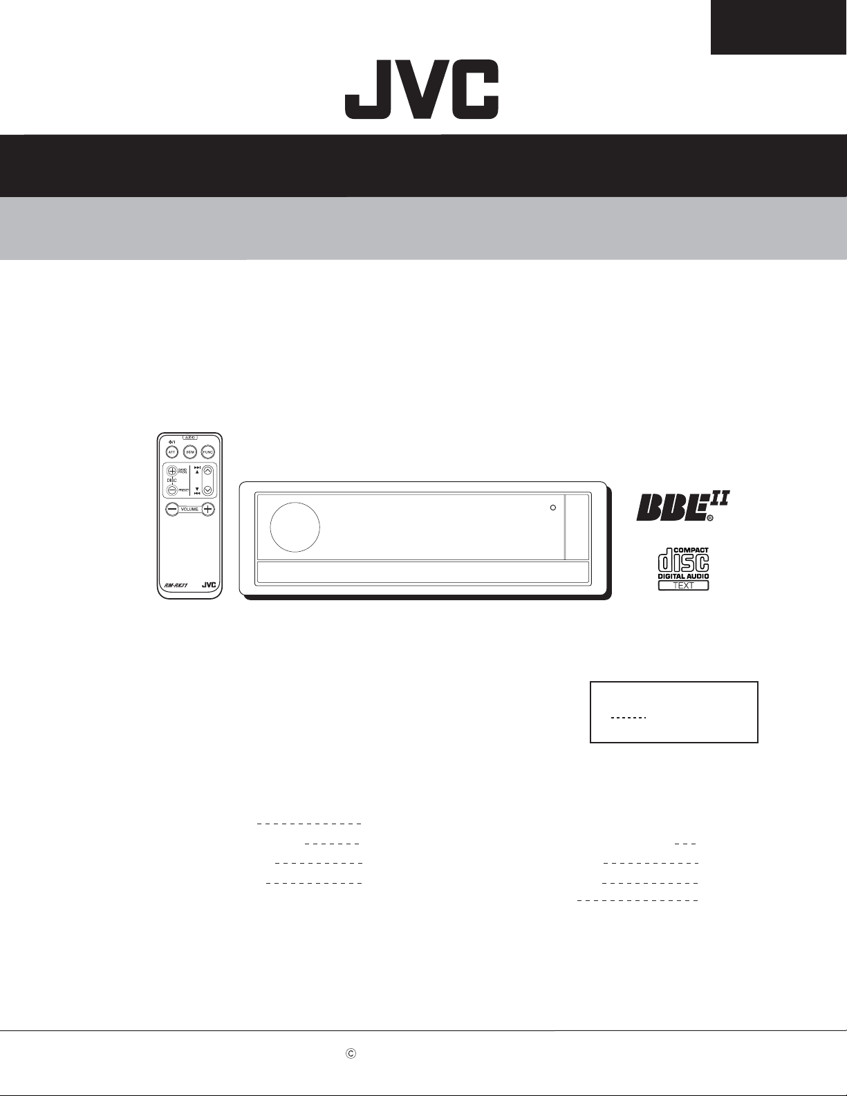
SERVICE MANUAL
CD RECEIVER
KD-LX333
KD-LX333
Contents
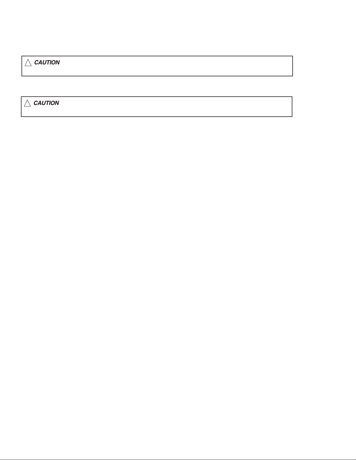
Safety precaution
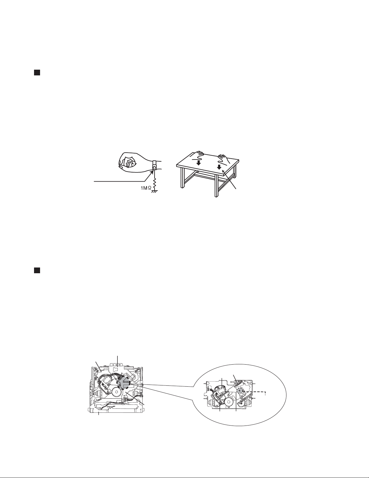
Preventing static electricity
Disassembly method
Adjustment method
1-2
1-3
1-4
1-13
COPYRIGHT 2002 VICTOR COMPANY OF JAPAN, LTD.
Flow of finctional operation intil opelation
until TOC read
Maintenance of laser pickup
Replacement of laser pickup
Description of Major ICs
Area Suffix
J Northern America
1-14
1-16
1-16
1-17~33
No.49722
Jun. 2002
Page 2
KD-LX333
Safety precaution
!
!
Burrs formed during molding may be left over on some parts of the chassis. Therefore,
pay attention to such burrs in the case of preforming repair of this system.
Please use enough caution not to see the beam directly or touch it in case of an
adjustment or operation check.
1-2
Page 3
KD-LX333
Preventing static electricity
Electrostatic discharge (ESD), which occurs when static electricity stored in the body, fabric, etc. is discharged,
can destroy the laser diode in the traverse unit (optical pickup). Take care to prevent this when performing repairs.
Grounding to prevent damage by static electricity
Static electricity in the work area can destroy the optical pickup (laser diode) in devices such as mechanism unit.
Be careful to use proper grounding in the area where repairs are being performed.
1. Ground the workbench
Ground the workbench by laying conductive material (such as a conductive sheet) or an iron plate over
it before placing the traverse unit (optical pickup) on it.
2. Ground yourself
Use an anti-static wrist strap to release any static electricity built up in your body.
(caption)
Anti-static wrist strap
Conductive material
(conductive sheet) or iron plate
3. Handling the optical pickup
1. In order to maintain quality during transport and before installation, both sides of the laser diode on the
replacement optical pickup are shorted. After replacement, return the shorted parts to their original condition.
(Refer to the text.)
2. Do not use a tester to check the condition of the laser diode in the optical pickup. The tester's internal power
source can easily destroy the laser diode.
Handling the traverse unit (optical pickup)
1. Do not subject the traverse unit (optical pickup) to strong shocks, as it is a sensitive, complex unit.
2. Cut off the shorted part of the flexible cable using nippers, etc. after replacing the optical pickup. For specific
details, refer to the replacement procedure in the text. Remove the anti-static pin when replacing the traverse
unit. Be careful not to take too long a time when attaching it to the connector.
3. Handle the flexible cable carefully as it may break when subjected to strong force.
4. It is not possible to adjust the semi-fixed resistor that adjusts the laser power. Do not turn it
CD mechanism ass’y
Damper bracket
Front bracket
CD mechanism
control board
Feed motor ass’y
FD gear
FD screw
Soldering
Pickup unit
1-3
Page 4
KD-LX333
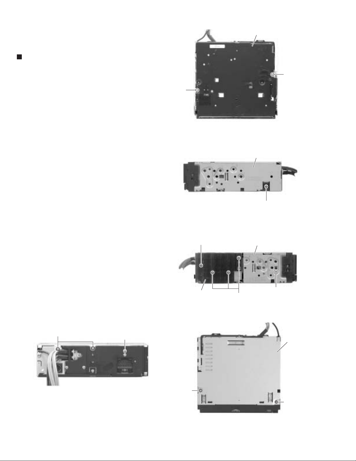
Disassembly method
<Main body>
Removing the top chassis
(See Fig.1 to 5)
1.
Remove the two screws A attaching the bottom
cover to the top chassis on the bottom of the body.
2.
Remove the two screws B attaching the top chassis
on both sides of the body.
3.
Remove the two screws C and the two screw D
attaching the heat sink on the left side of the body.
4.
Remove the two screws E and the screw F on the
back of the body.
5.
Remove the two screws G on the upper side of the
body.
6.
Move the top chassis upward and disconnect the CD
mechanism connector from the main board
connector by pulling it. Remove the top chassis from
the body.
Bottom cover
A
A
Fig.1
Top chassis
B
Fig.2
E
Fig.4
F
C
Heat sink
G
Top chassis
B
D
Fig.3
Top chassis
G
1-4
Fig.5
Page 5
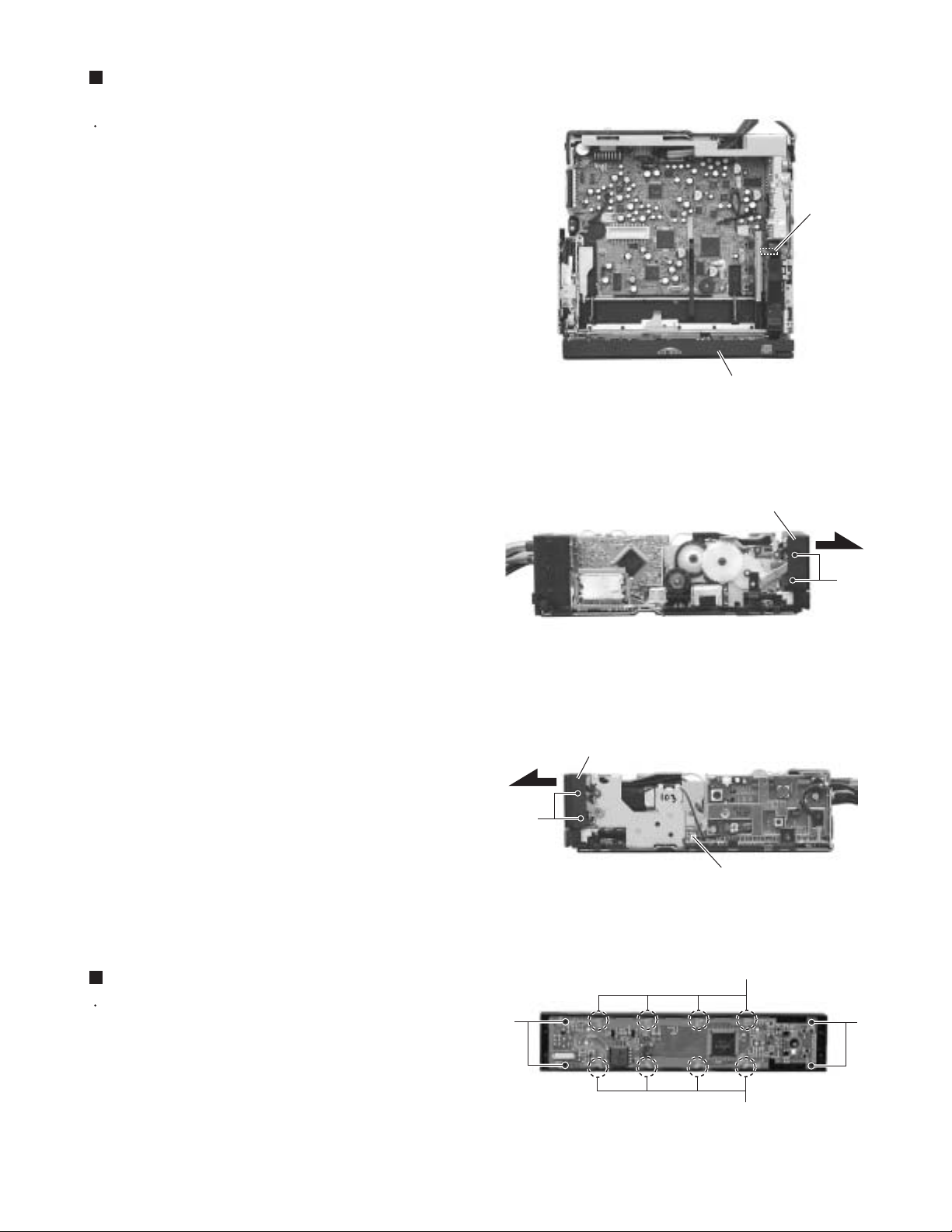
Removing the front panel assembly
(See Fig.6 to 8)
Prior to performing the following procedure, remove
the top chassis assembly.
1.
Disconnect the flexible harness from connector
CN701 on the main board assembly.
2.
Remove the four screws H attaching the front panel
assembly on both sides of the body. Remove the
front panel toward the front.
KD-LX333
CN701
Front panel assembly
Fig.6
Front panel assembly
H
Front panel assembly
H
Fig.7
CN701
Fig.8
Removing the Front Board (See Fig.9)
Prior to performing the following procedure, remove
the top chassis assembly and the front panel
assembly.
1.
Remove the four screws I attaching the front board
on the back of the front panel assembly and release
the eight joints a.
Joints a
I
Joints a
Fig.9
I
1-5
Page 6
KD-LX333
Removing the lifter unit (See Fig.10)
Prior to performing the following procedure, remove
the top chassis assembly and the front panel
assembly.
1.
Disconnect the harness from connector CN503and
CN504 on the main board.
2.
Remove the four screws J and detach the lifter unit
from the bottom cover.
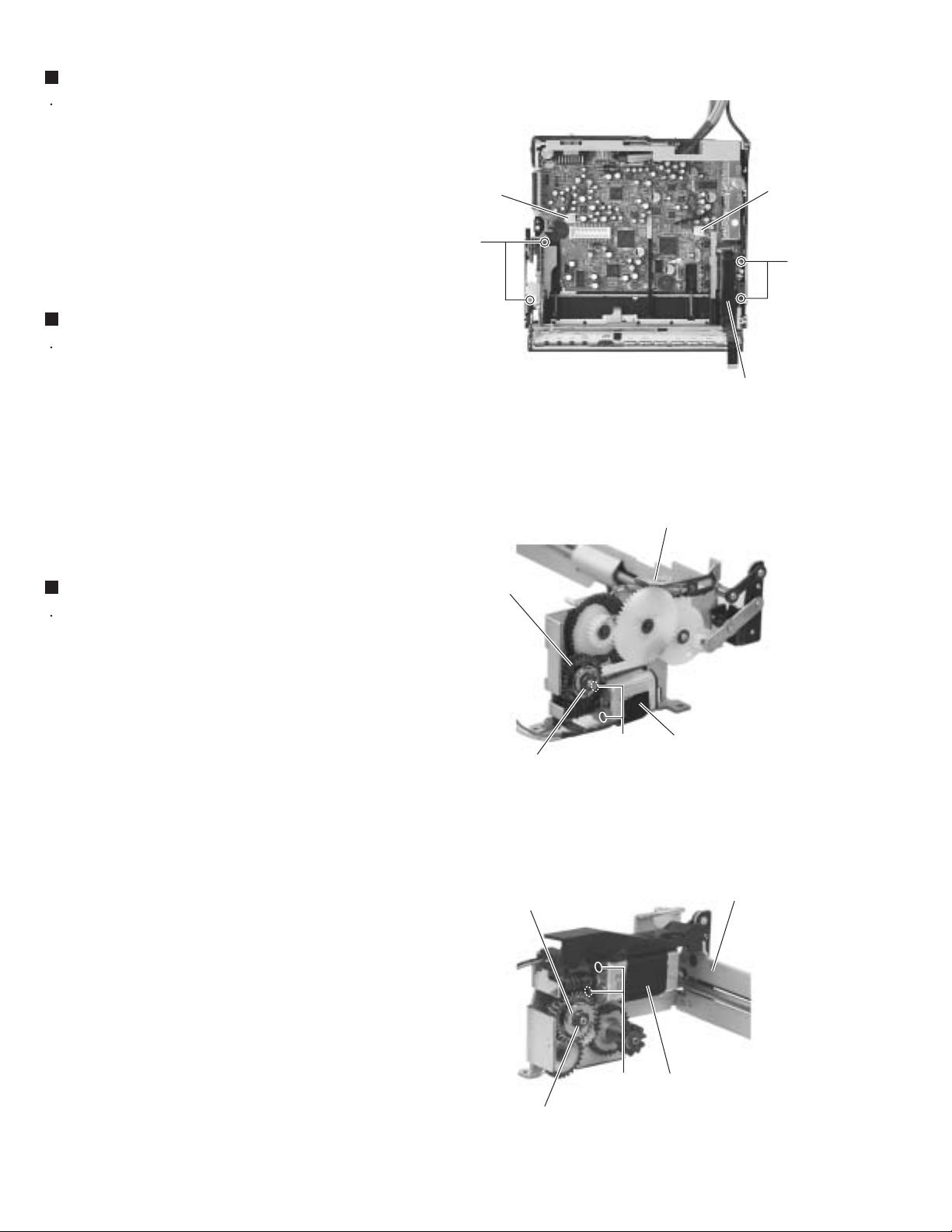
Removing the feed motor (L) (See Fig.11)
Prior to performing the following procedure, remove
the lifter unit.
1.
Remove the washer attaching the clutch assembly
and detach the clutch assembly from the shaft of the
lifter unit.
2.
Remove the two screws K attaching the feed motor
(L).
CN503
J
CN504
J
Lifter unit assembly
Fig.10
Lifter unit assembly
Removing the feed motor (R) (See Fig.12)
Prior to performing the following procedure, remove
the lifter unit.
1.
Remove the washer attaching the clutch assembly
and detach the clutch assembly from the shaft of the
lifter unit.
2.
Remove the two screws L attaching the feed motor
(R).
Clutch assembly
Washer
Clutch assembly
Feed motor (L) assembly
K
Fig.11
Lifter unit assembly
1-6
Washer
Feed motor (R) assembly
L
Fig.12
Page 7
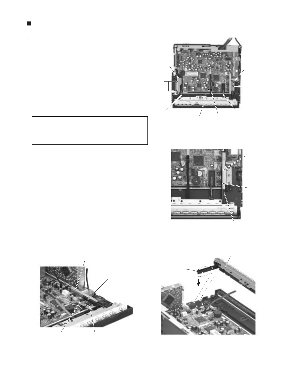
Removing the operation assembly
(See Fig.13 to 16)
Prior to performing the following procedure, remove
the top chassis assembly, the front panel assembly
and the lifer unit.
1.
Disconnect the card wire from connector CN702 on
the main board and remove the operation assembly.
2.
Remove the three screws M attaching the right and
left brackets which fix gears on both sides of the
operation assembly.
3.
Remove the springs 5 and 6 from the operation
assembly.
ATTENTION:
When reassembling, correctly engage
the switch S651 and S652 on the
main board and the right gear with
the part b of the operation assembly.
Bracket (L)
M
Spring 5
Operation assembly
Fig.13
KD-LX333
Bracket (R)
M
Spring 6
CN702
Bracket (R)
Operation assembly b
S652
S651
Operation assembly b
Fig.14
Operation assembly
b
S652
S651
Fig.15Fig.16
1-7
Page 8
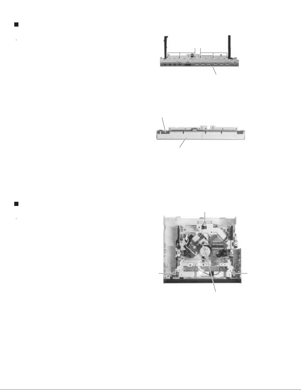
KD-LX333
Removing the operation switch board
(See Fig.17 and 18)
Prior to performing the following procedure, remove
the operation assembly.
1.
Remove the six screws N attaching the button panel
on the operation assembly.
2.
Pull out the operation switch board from inside of the
button panel.
NN
Button panel
Fig.17
Operation switch board
Button panel
Removing the CD mechanism assembly
(See Fig.19)
Prior to performing the following procedure, remove
the top chassis.
1.
Remove the three screws O and the CD mechanism
assembly from the top chassis.
O
Fig.18
O
O
CD mechanism assembly
1-8
Fig.19
Page 9
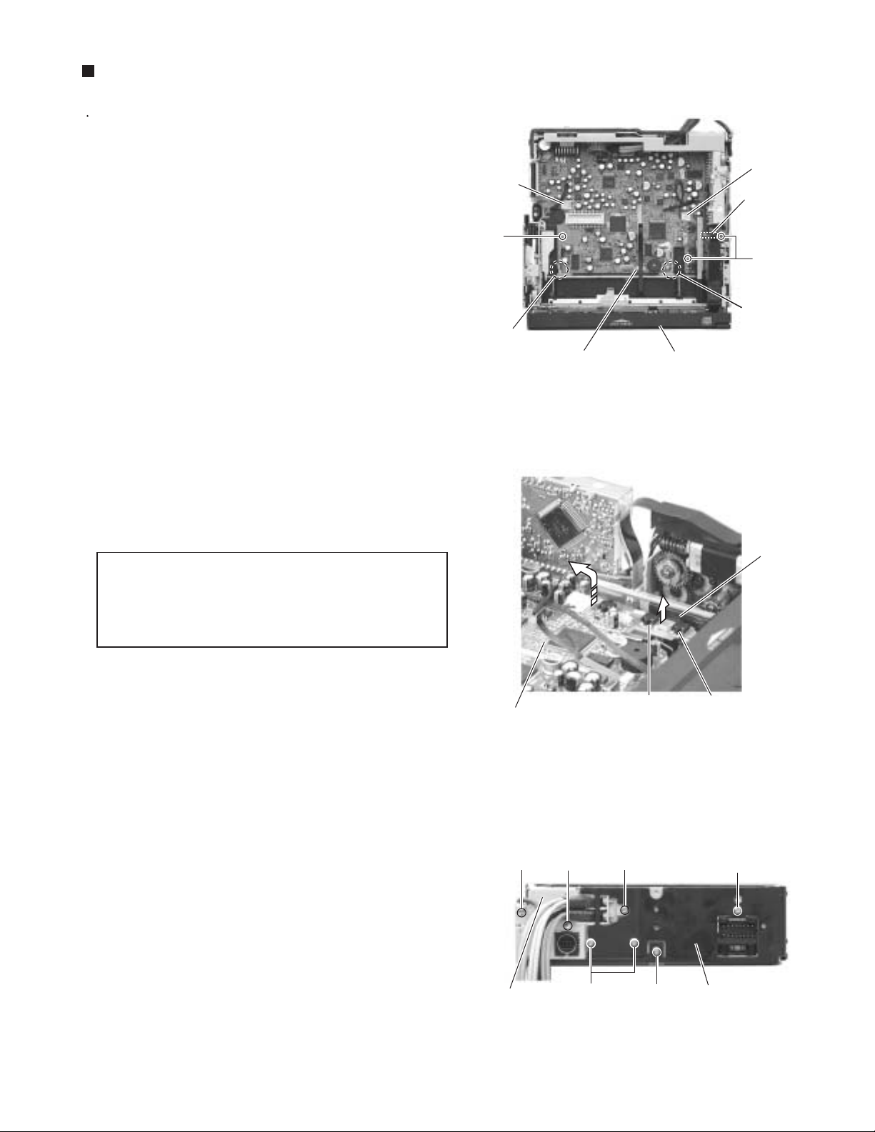
Removing the main board assembly
(See Fig.20 to 22)
Prior to performing the following procedure, remove
the top chassis.
KD-LX333
1.
Disconnect the flexible harness from connector
CN701, the card wire from CN702 on the main board
and the harness from CN503 and CN504
respectively.
2.
Remove the three screws P attaching the main
board assembly to the bottom cover on the upper
side of the body.
3.
Remove the screw Q attaching the rear panel and
the bottom cover on the back of the body. Move the
main board in the direction of the arrow and release
the two joints c. (At this point, the main board can be
removed with the rear panel and the rear heat sink.)
4.
Remove the three screws R attaching the rear heat
sink on the back of the body.
5.
Remove the two screws S and the screw T
attaching the rear panel. Now, the main board
assembly will be removed.
ATTENTION:
When reassembling, correctly engage
the switch S651 and S652 on the
main board and the right gear with
the part b of the operation assembly
(Refer to Fig.21).
CN503
P
Joint c
CN702
CN504
CN701
P
Joint c
Front panel assembly
Fig.20
b
Main board
S
Rear panel
T
S652
Fig.21
S
Fig.22
QR
S651
R
Rear heat sink
1-9
Page 10
KD-LX333
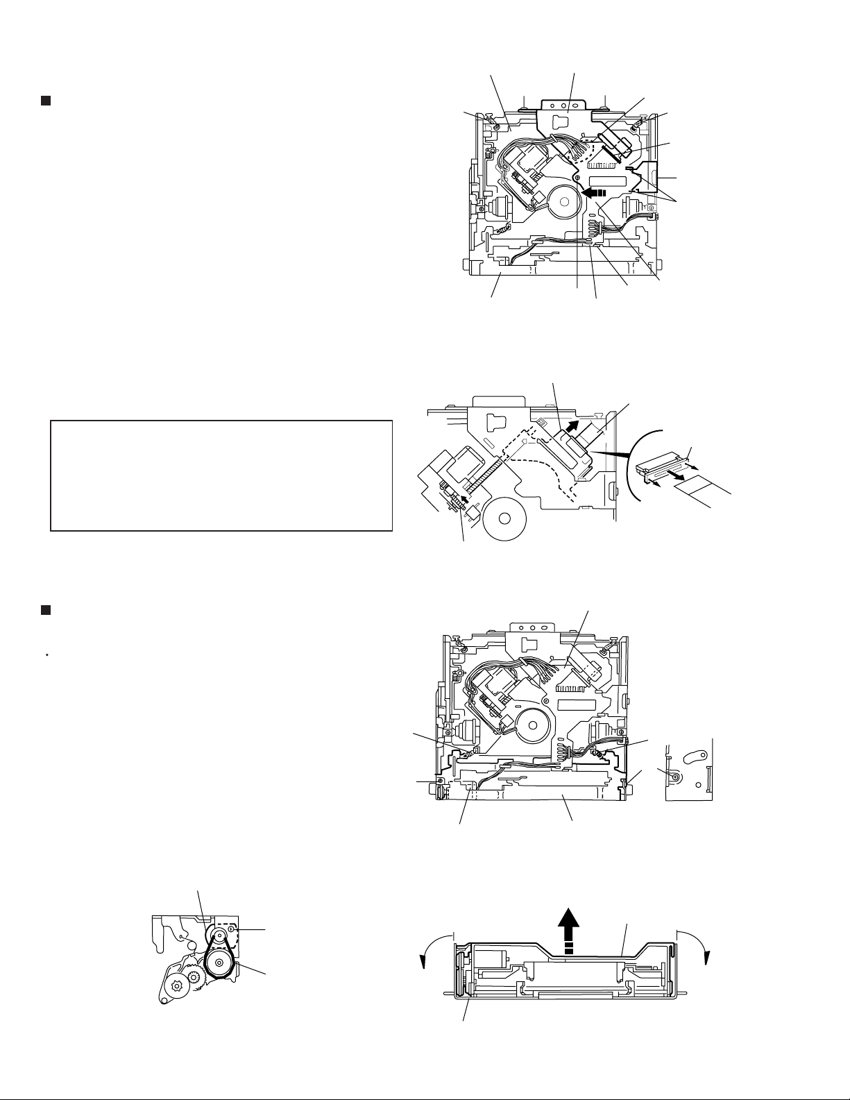
<CD mechanism section>
Removing the CD mechanism control
board (See Fig.1 and 2)
1.
Unsolder the part a and b on the CD mechanism
control board.
2.
Remove the stator fixing the CD mechanism control
board and the damper bracket (To remove the stator
smoothly, pick up the center part).
3.
Remove the screw A attaching the CD mechanism
control board.
4.
Remove the CD mechanism control board in the
direction of the arrow while releasing it from the two
damper bracket slots d and the front bracket slot e.
5.
Disconnect the flexible wire from connector on the
pickup unit.
ATTENTION:
Turn the FD gear in the direction of the
arrow to move the entire pickup unit to
the appropriate position where the
flexible wire of the CD mechanism unit
can be disconnected easily.
(Refer to Fig.2)
CD mechanism assembly
D
h
Front bracket
Pickup unit
Damper bracket
D
A
Fig.1
e
b
Flexible wire
a
h
c
D
d
CD mechanism
control board
Shift the lock
Removing the loading motor
(See Fig.3 to 5)
Prior to performing the following procedure, remove
the CD mechanism control board.
1.
Remove the two springs f attaching the CD
mechanism assembly and the front bracket.
2.
Remove the two screws B and the front bracket
while pulling the flame outward.
3.
Remove the belt and the screw C from the loading
motor.
Loading motor
C
FD gear
f
B
Loading motor
Pull outward
Fig.2
CD mechanism control board
f
B
Front bracket
Fig.3
Front bracket
Pull outward
1-10
Fig.5
Belt
Flame
Fig.4
Page 11
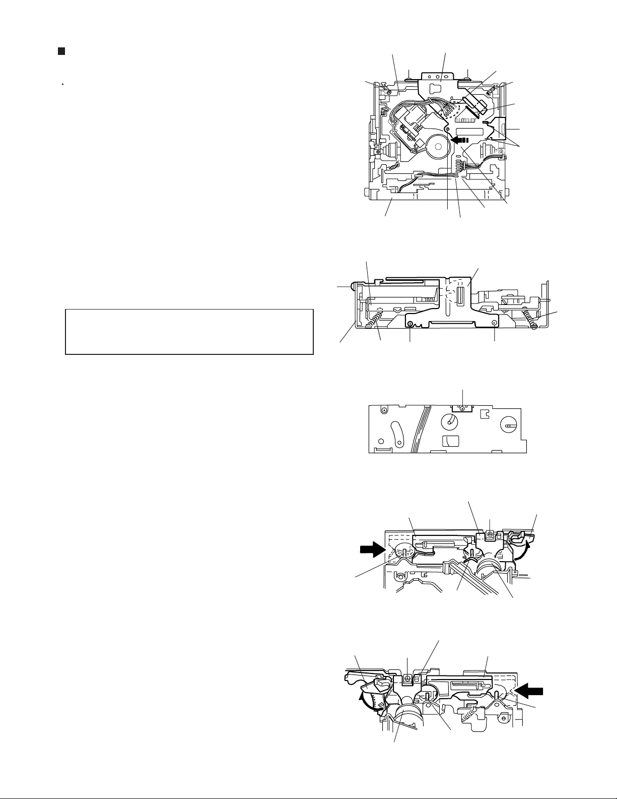
KD-LX333
Removing the CD mechanism assembly
(See Fig.1, 6 to 9)
Prior to performing the following procedure, remove
the CD mechanism control board and the front
bracket (loading motor).
1.
Remove the three screws D and the damper
bracket.
2.
Raise the both sides fix arms and move the fix plates
in the direction of the arrow to place the four shafts g
as shown in Fig.8 and 9.
3.
Remove the CD mechanism assembly and the two
springs h attaching the flame.
4.
Remove the two screws E and both sides rear
damper brackets from the dampers. Detach the CD
mechanism assembly from the left side to the right
side.
ATTENTION:
The CD mechanism assembly can be
removed if only the rear damper
bracket on the left side is removed.
CD mechanism
h
Front bracket
CD mechanism
D
Flame
assembly
D
assembly
h
D
Damper bracket
D
A
Fig.5
e
b
Damper bracket
D
Fig.6
a
h
c
D
d
CD mechanism
control board
h
Fix plate (L)
g
Fix arm (R)
D
Fig.7
Rear damper bracket
g
Fig.8
Rear damper bracket
E
Fix plate(R)
E
Fix arm (L)
Damper
Damper
g
g
Fig.9
1-11
Page 12

KD-LX333
Removing the feed motor assembly
(See Fig.10)
Prior to performing the following procedure, remove
the CD mechanism control board, the front bracket
(loading motor) and the CD mechanism assembly.
1.
Remove the two screws F and the feed motor
assembly.
Removing the pickup unit
(See Fig.10 and 11)
Prior to performing the following procedure, remove
the CD mechanism control board, the front bracket
(loading motor), the CD mechanism assembly and
the feed motor assembly.
1.
Detach the FD gear part of the pickup unit upward.
Then remove the pickup unit while pulling out the
part i of the FD screw.
Feed motor assembly
F
FD gear
Nut push spring plate
FD screw
Pickup unit
Fig.10
Part i
Part j
Pickup unit
G
Pickup mount nut
Pickup unit
ATTENTION:
2.
Remove the screw G attaching the nut push spring
plate and the pickup mount nut from the pickup unit.
Pull out the FD screw.
When reattaching the pickup unit,
reattach the part j of the pickup unit,
then the part i of the FD screw.
Removing the spindle motor
(See Fig.12 and 13)
Prior to performing the following procedure, remove
the CD mechanism control board, the front bracket
(loading motor), the CD mechanism assembly and
the feed motor assembly.
1.
Turn up the CD mechanism assembly and remove
the two springs k on both sides of the clamper arms.
Open the clamper arm upward.
2.
Turn the turn table, and remove the two screws H
and the spindle motor.
FD screw
k
Spindle motor
Fig.11
k
Fig.12
H
1-12
H
Fig.13
Page 13

Adjustment method
KD-LX333
Test instruments required adjustment
1.Digital oscilloscope (100MHz)
2.AM Standard signal generator
3.FM Standard signal generator
4.Stereo modulator
5.Electric voltmeter
6.Digital tester
7.Test disc(CTS-1000)
8.Extension cable for check
EXTGS004-22P
Standard volume position
Balance and Bass & Treble volume : Indication "0"
Loudness : OFF
requency Band
F
FM: 87.5 MHz to 107.9 MHz
(with channel interval set to 200 kHz)
87.5 MHz to 108.0 MHz
(with channel interval set to 50 kHz)
AM: 530 kHz to 1710kHz
(with channel interval set to 10 kHz)
531 kHz to 1602 kHz
(with channel interv
Dummy load
Exclusive dummy load should be used for AM, and FM.
For FM dummy load, there is a loss of 6dB between SSG output
and antenna input. The loss of 6dB need not be considered
since direct reading of figures are applied in this workingo
standard.
Standard measuring conditions
Power supply voltage DC 14.4V(11V to 16V allowance)
Load impedance 4 (4 to 8 allowance)
Line-out Level/Impedance
: 2.0 V/20k load(full scale)
Output impedance : 1k
al set to 9 kHz)
EXTLX002-JIG : Kit including the following 8 extension parts.
No.
1
2
3
4
5
6
7
Parts number Quantity Description
EXTLX001-2P
EXTLX001-6PF
EXTLX001-6PC
EXTLX002-16PF
EXTLX002-16PC
EXTLX002-SWPWB
EXTLX002-4P
2
1
1
1
1
1
1
EXTGS004-26P
EXTLX001-16PF
2Pin, 30cm extension cord
6Pin, 30cm flat wire
6Pin x 2, interlocking connector
16Pin flat wire
16Pin, interlocking connector
3 switch PWB
4Pin, 30cm extension cord
EXTLX002-4P
EXTLX002-SWPWB
EXTLX002-16PC
EXTLX001-2P
EXTLX001-6PC
EXTLX001-2P
EXTLX001-6PF
1-13
Page 14

KD-LX333
Flow of functional operation until TOC read
Power ON
When the pickup correctly moves
v
to the inner area of the disc
Set Function CD
When the laser diode correctly
emits
Microprocessor
commands
FMO
TC94A14FA" 40"
FEED MOTOR
+TERMINAL
IC501"4"
REST SW
When correctly focused
FEO
TA2157" 15"
Focus Servo Loop ONo
$83
$82
$81
3.3V
Hi-Z
0V
6V
4V
2V
OFF
ON
Pickup feed to the inner area
2.2V
RF signal eye-patternn
remains closed
RF signal eye-pattern
opens
Disc inserted
YES
Laser emitted
Focus search
Disc rotates
Tracking loop closed
TOC read out
YES
Microprocessor
commands
SEL
TC94A14FA"38"
LD
CN501"15"
"No disc"
display
When the disc correctly rotates
Microprocessor
commands
DMO
TC94A14FA"41"
Spindle
motor(-)
IC501"7"
$84 $86 $ A200
Acceleration Servo CLV
Rough
Servo
0.5 Sec 0.5 Sec
$84
3.3V
0V
4V
0V
3.3V
2.2V
0V
6V
3.2
2V
1-14
Jump to the first track
Play
Tracking Servo Loop ON
RF signal
Rough Servo Modev
CLV Servo Mode
(Program Area)
CLV Servo Mode
(Lead-In Area;
Digital :0)
Page 15

Feed section
Is the voltage output at
IC541 pin "40" 5V or 0V?
YES
Is 4V present at both
sides of the feed motor?
YES
NO YES NO
NO
Is the wiring for IC541
(56)~(64) correct?
NO
Is 6V or 2V present at
IC501 "4" and "5"?
NO
Is 3.3V present at IC501
pin "20"?
Check the vicinity of
IC541.
YES
Check the feed motor
connection wiring.
YES
Check CD 8V
KD-LX333
and 5V.
Check the feed motor.
Focus section
When the lens is
moving:
4V
Does the S-search
waveform appear at
IC501 pins "8" and "9"?
Spindle section
Is the disk rotated?
YES
Does the RF signal
appear at TP1?
YES
Is the RF waveform at TP1
distorted?
YES
Proceed to the Tracking
section
Check IC501.
NO
YES
NO
NO
NO
Check the circuits in
the vicinity of IC501
pins "8","9"and"15".
Check the pickup and
its connections
Is 4V present at IC501
pins "6" and "7"?
Check the spindle motor
and its wiring
Check the circuits in the
vicinity of IC521 "19"~
"24" or the pickup
YES
YES
NO
Is 4V present at IC541
pins "41" ?
Check the vicinity of
IC501.
NO
YES
Check IC541 and
IC521.
racking section
T
When the disc is rotated
Is the tracking error signal
output at IC521 "11"?
Check IC541.
at first:
Approx. 1.2V
YES
YES YES
Check the circuit in the
vicinity of IC521 pins
"2"~"12".
Check the pickup and
its connections
1-15
Page 16

KD-LX333
Maintenance of laser pickup
(1) Cleaning the pickup lens
Before you replace the pickup,please try to
clean the lens with a alcohol soaked cotton
swab.
(2) Life of the laser diode
When the life of the laser diode has expired.
the following symptoms will appear..
(1) The level of RF output (EFM output:amplitude
of eye patterrn) will be low.
Is RF output
1.3 0.4Vp-p?
YES
O.K
(3) Semi-fixed resistor on the APC PC board
The semi-fixed resistor on the APC printed
circuit board which is attached to the pickup
is used to adjust the laser power.Since this.
adjustment should be performed to match the
characteristics of the whole optical block,
do not touch the semi-fixed resistor..
If the laser power is lower than the specified
value, the laser diode is almost worn out, and
the laser pickup should be replaced.
If the semi-fixed resistor is adjusted while
the pickup is functioning normally, the laser
pickup may be damaged due to excessive current.
NO
Replace it.
Replacement of laser pickup
Turn of the power switch and, disconnect the
power cord.
Replace the pickup with a normal one.(Refer
to "Pickup Removal" on the previous page)
Plug the power cord in, and turn the power on.
At this time, check that the laser emits for
about 3seconds and the objective lens moves
up and down.
Note: Do not observe the laser beam directly..
1-16
Play a disc.
Check the eye-pattern at TP1.
Finish.
Page 17

Description of major ICs
/
TC9490FA (IC521) : DSP & DAC
1.Pin layout & Block daiagram
KD-LX333
DV
SS3
RO
DV
DD3
DVR
LO
DV
SS3
ZDET
SS5
V
BUS0
BUS1
BUS2
BUS3
BUCK
/CCE
/RST
VXDD3XOXI
SS3
XV
TEIN
DD3VSS3
V
DMO
FMO
DD3
AV
SEL
TEBC
RFGC
48 47 46 45 44 43 42 41 40 39 38 37 36 35 34 33
49
50
51
52
LPF
Clock
generator
1-bit
DAC
PWM
Servo control
A/D
53
54
55
56
Address
circuit
ROM
RAM
Digital equalizer
automatic
adjustment circuit
57
58
59
60
61
62
Micro-
controller
interface
circuit
Correction
Audio output
circuit
16k
RAM
Digital output
CLV servo
Sync signal
protection
EFM
Sub code
detector
TMAX
63
VCO
PLL
REF
V
D/A
Data
slicer
TRO
FOO
32
31
30
29
28
27
26
25
24
23
22
21
20
19
18
TEZI
TEI
SBAD
FEI
RFRP
RFZI
RFCT
DD3
AV
RFI
SLCO
AV
SS3
VCOF
REF
RV
LPFO
LPFN
64
DD5
V
17
TMAX
1 2 3 4 5 6 7 8 9 10 11 12 13 14 15 16
BCK
LRCK
AOUT
DOUT
IPF
DD3
V
V
SBOK
CLCK
DATA
SFSY
SBSY
/HSO
UHSO
DD3
PV
PDO
SS3
1-17
Page 18

KD-LX333
2.Pin function (1/2)
Pin No.
1
2
3
4
Symbol
BCK
LRCK
AOUT
DOUT
5
6
7
8
9
10
11
12
13
14
VDD3
VSS3
SBOK
CLCK
DATA
SFSY
SBSY
/HSO
/UHSO
IPF
I/O
O
O
O
O
O
-
-
O
I/O
O
O
O
O
O
TC9490FA(2/3)
Function
Bit clock outputpin 32fs, 48fs, or 64fs selectable by command.
L/R channel clock output pin."L" for L channe and "H" for R channel.
Output polarity can be inverted by command.
Audio data output pin. MSB-first or LSB-first selectable by command.
Digital data output pin. Outputs up to double-speed playback.
Correction flag output pin.When set to "H",AOUT output cannot be corrected
by C2 correction processing.
Digital 3.3V power supply voltage pin.
Digital GND pin.
Subcode Q data CRCC result output pin."H" level when result is OK.
Subcode P-W data read clockI/O pin. I/O polarity selectable by command.
Subcode P-W data output pin.
Playback frame sync signal output pin.
Subcode block sync signal output pin. "H" level at S1 when subcode sync is
detected.
Playback speed mode flag output pins.
/HSO
H
H
L
--
H
L
L
--
Playback speed/UHSO
Normal
Double
4 times
---
15
16
17
18
19
20
21
22
23
24
25
26
27
28
29
30
31
32
33
34
35
PVDD3
PDO
TMAX
LPFN
LPFO
PVREF
VCOF
SS3
AV
SLCO
RFI
AV
RFCT
RFZI
RFRP
FEI
SBAD
TEI
TEZI
FOO
TRO
REF
V
-
PLL-only 3.3V power supply voltage pin.
O
EFM and PLCK phase difference signal output pin.
O
TMAX detection result output pin.
TMAX OutputTMAX Detection result
Longer than fixed period
Within fixed period
Shorter than fixed period
I
Inverted input pin for PLL LPF amp.
O
Output oin for PLL LPF amp.
-
PLL-only V
VCO filter pin.
O
Analog GND pin.
DAC output pin for data slice level generation.
O
RF signal input pin.Zin selectable by command.
I
Analog 3.3V power supply voltage pin.
RFRP signal center level input pin.
I
RFRP signal zero-cross input pin.
I
RF ripple signal input pin.
I
Focus error signal input pin.
I
Sub-beam adder signal input pin.
I
Tracking error input pin. Inputs when tracking servo is on.
I
Tracking error signal zero-cross input pin.
I
Focus equalizer output pin.
O
Tracking equalizer output pin.
O
Analog reference power supply voltage pin.
-
REF pin.
"PVDD3"
"HIZ"
"AV
SS3"
1-18
Page 19

KD-LX333
2.Pin function (2/2)
Pin No.
36
37
38
39
40
41
42
43
44
45
Symbol
RFGC
TEBC
SEL
AV
FMO
DMO
V
V
TESIN
XV
46
47
48
49
XV
DV
50
51
52
DV
DVR
53
54
55
56
57
58
59
60
61
62
63
64
DV
ZDET
V
BUS0
BUS1
BUS2
BUS3
BUCK
/CCE
/RST
V
DD3
SS3
DD3
XI
XO
DD3
RO
DD3
LO
SS5
DD5
SS3
SS3
SS3
I/O
O
O
O
O
O
-
-
I
-
I
O
-
O
-
O
O
-
I/O
I
I
I
-
TC9490FA(3/3)
Function
RF amplitude adjustment control signal output pin.
Tracking balance control signal output pin.
APC circuit ON/OFF signal output pin. At laser on,high impedance with
UHS="L" ,H output with UHS="H".
Analog 3.3V power supply voltage pin.
Feed equalizer output pin.
Disc equalizer output pin.
Digital GND pin.
Digital 3.3V power supply voltage pin.
Test input pin. Normally,fixed to "L".
System clock oscillator GND pin.
System clock oscilatoe input pin.
System clock oscillator output pin.
System clock oscillator 3.3V power supply voltage pin.
DA converter GND pin.
R-channel data forward output pin.
DA converter 3.3V power supply pin.
Reference voltage pin.
L-channel data forward output pin.
DA converter GND pin.
1 bit DA converter zero data detection flag output pin.
Microcontroller interface GND pin.
Microcontroller interface data I/O pins.
Microcontroller interface clock input pin.
Microcontroller interface chip enable signal input pin.At "L".
Bus0 to BUS3 are active.
Reset signal input pin. At reset,"L".
Microcontroller interface 5V power supply pin.
NJM4565MD (IC151,IC171,IC323) : Operational amp
+
A OUTPUT
-
A INPUT
+
A INPUT
V
1
2
3
-
4
8
V
B OUTPUT
7
B INPUT
-
6
5
+
B INPUT
1-19
Page 20

KD-LX333
UPD784215AGC101 (IC701) : Main micon
1.Pin layout
100 ~ 76
1
75
~
25
26 ~ 50
2.Pin functions(1/3)
Pin No.
1
2
3
4
5
6
7
8
9
10
11
12
13
14
15
16
17
18
19
20
21
22
23
24
25
26
27
28
29
30
31
32
33
34
35
36
37
38
39
40
41
42
Symbol
SW2
SW3
SW4
RST-SW
LMO
LM1
DIM-OUT
ILLUM1
VDD
X2
X1
VSS
XT2
XT1
RESET
SW1
BUS-INT
PS2
CRUISE
NC
NC
REMOCON
AVDD
AVREFO
TEM1
KEY0
KEY1
KEY2
LEVEL
NC
SQ
SM
AVSS
W-VOL
DOT-CNT
AVREF
BUS-SI
BUS-SO
BUS-SCK
STAGE2
LCD-DA
LCD-SCK
~
51
I/O
Function
I
CD mechanical switch 2 detection signal input
I
CD mechanical switch 3 detection signal input
I
CD mechanical switch 4 detection signal input
I
Rest switch detection signal input
O
Motor signal control signal output at loading
O
Motor signal control signal output at leject
O
DIMMER pulse control output
O
POWER ON:H,FLAT PANEL:L
-
5V
-
-
-
GND
-
I
Reset detection teaminal
I
CD mechanical switch 1 detection signal input
I
J-BUS int
I
POWER SAVE2. Operating together with BACKUP.H input:STOP
I
Pulse signal for CRUISE input(only in 330R)
-
I
Remocon input
-
5V
-
5V
I
Temperature detection input
I
Key input 0
I
Key input 1
I
Key input 2
I
Level meter input
I
S.QUALITY level input
I
S.METER level input
-
GND
O
Subwoofer volume control analog output
O
Dot matrix contrast adjustment analog output
-
5V
I
J-BUS data input
O
J-BUS data output
I/O
J-BUS clock input and output
I
H:LX300 L:LX100
O
Data output to LCD driver
O
Clock output to LCD driver
1-20
Page 21

2.Pin functions(2/3)
KD-LX333
Pin No.
43
44
45
46
47
48
49
50
51
52
53
54
55
56
57
58
59
60
61
62
63
64
65
66
67
68
69
70
71
72
73
74
75
76
77
78
79
80
81
82
83
84
85
86
87
88
89
90
91
92
93
94
Symbol
LCD-CE1
BUZZER
12C-DAI
12C-DAO
12C-CLK
BUS-I/O
TMO
TM1
DMO
DM1
ST
NC
MONO
C-SW1
C-SW2
C-SW3
C-SW4
C-SW5
VOL1
VOL2
SEEK/STP
NC
FM/AM
PLL-CE
PLL-DO
PLL-CLK
PLL-DI
NC
AMP-KILL
VSS
DIM -IN
PS1
POWER
CD-ON
MUTE
W-LPF1
W-LPF2
W-MUTE
VDD
VOL-DA
VOL-CLK
NC
GVSW
LCD RST
NC
DMK
TMK
NC
BUCK
CCE
RST
TEST
I/O
Function
O
Chip enable output 1 to LCD driver
O
Buzzer output
I
12C communication data input
O
12C communication data output
O
12C communication clock output
O
J-BUSI/O signal terminal
O
Tray motor negative signal output terminal
O
Tray motor positive signal output terminal
O
Motor control signal output in door down
O
Motor control signal output in door up
I
Stereo detector stereo signal input H:Brordcasting station L:Stereo
O
O
Monaural ON/OFF selection output MONO ON:H
I
Chameleon machanical switch 1 detection signal input
I
Chameleon machanical switch 2 detection signal input
I
Chameleon machanical switch 3 detection signal input
I
Chameleon machanical switch 4 detection signal input
I
Chameleon machanical switch 5 detection signal input
I
Rotary volume signal 1 input
I
Rotary volume signal 2 input
O
Auto seek/stop selection output SEEK:H STOP:L
O
-
FM/AM selection output FM:H AM:L
O
IC control CE output
O
IC control data output
O
IC control clock output
I
IC control data input
O
Telephone mute detection input
O
POWER AMP ON/OFF selection output
-
GND
I
Dimmer detection input L:dimmer ON
I
Power save 1 Operating together with ACC.Power save :L Operating :H
O
Power ON/OFF selection output Power ON:H
O
CD power supply control signal output CD:H
O
Mute output MUTEON:L
O
Subwoofer cut off frequency control output 1
O
Subwoofer cut off frequency control output 2
O
Subwoofer mute output MUTE ON:H
-
5V
O
data output terminal
O
clock signal output terminal
O
O
CD-DA/CD-RW selection control output CD-RW:L
O
Reset signal output to LCD driver
-
O
Door motor kick signal output
O
Tray motor kick signal output
-
O
Data cmmunication clock output with CDLSI
O
Data cmmunication clock CE with CDLSI
O
CDLSI reset signal output
-
GND
1-21
Page 22

KD-LX333
+
+
-
-
+
+
-
-
-
+
+
2.Pin functions(3/3)
Pin No.
95
96
97
98
99
100
Symbol
BUSO
BUS1
BUS2
BUS3
DISCSEL
NC
I/O
Function
I/O
Data communication input and output port 0 with CDLSI
I/O
Data communication input and output port 1 with CDLSI
I/O
Data communication input and output port 2 with CDLSI
I/O
Data communication input and output port 3 with CDLSI
I
H:not for 8cm DISC L:for 8cm DISC
O
BA3220FV-X (IC301,IC401) : Line out amp
1.Pin layout
14
3220
17
8
2.Block diagram
1
CL-
14
LGND
13
REFL
2
Vcc
OUTL OUTR RGND
3
INL
1112
4
NFLCL+
10
REFR
FILTER
56
FIL
CR-
9
NFR
CR+
8
7
INR
1-22
Page 23

BD3860K (IC911) : E.Vol & Loud
1.Terminal layout
33 23
KD-LX333
2.Block diagram
GND FIL VCC SEL1
6 5 9 40 36 35 343328323130 2919 15 14
POWER
SUPPLY
A1
41
B1
42
C1
43
D1
44
INPUT
1
2
3
4
SELECTOR
A2
B2
C2
D2
34
44
1 11
INPUT
GAIN
0 18 dB
INPUT
GAIN
0 18 dB
22
12
VIN1 LOUD1 HF1 LF1 DET1 TIN1 TNF1 BNF1
MAIN
VOLUME
0 -40 dB
LOUDNESS
MAIN
VOLUME
0 -40 dB
LOUDNESS
LOW(f=50Hz) 6dB
PROCESS CONTROL +3 to 12dB
(f=10kHz)
LOGIC
LOW(f=50Hz) 6dB
PROCESS CONTROL +3 to 12dB
(f=10kHz)
TREBLE
-14 +14dB
TREBLE
-14 +14dB
-14 +14dB
-14 +14dB
BASS
BASS
BOUT1VCA1 MIX1 BBOUT1
FADER
CH1 FRONT
0 -5 dB
FADER
CH1 REAR
0 -5 dB
FADER
CH2 REAR
0 -5 dB
FADER
CH2 FRONT
0 -5 dB
13
12
37
10
11
7
8
OUTF1
OUTR1
SI
SC
OUTR2
OUTF2
3.Pin function
Pin
Symbol Function
No.
1
2
3
4
5
6
7
8
9
10
11
12
13
14
15
16
17
18
19
20
21
22
A2
B2
C2
D2
FIL
GND
SI
SC
VCC
OUTR2
OUTF2
OUTR1
OUTF1
BOUT1
BNF1
BOUT2
BNF2
TNF2
TNF1
TIN2
BBOUT2
MIX2
CH2 Input Pin A
CH2 Input Pin B
CH2 Input Pin C
CH2 Input Pin D
1/2 VCC Pin
Ground Pin
Serial Data Receiving Pin
Serial Clock Receiving Pin
Power Supply Pin
CH2 Rear Output Pin
CH2 Front Output Pin
CH1 Rear Output Pin
CH1 Front Output Pin
CH1 Bass Filter Setting Pin
CH1 Bass Filter Setting Pin
CH2 Bass Filter Setting Pin
CH2 Bass Filter Setting Pin
CH2 Treble Filter Setting Pin
CH1 Treble Filter Setting Pin
CH2 Treble Input Pin
CH2 BBE II Signal Output Pin
CH2 Output MIX Amplifier
Inverse Input Pin
39 38 37 25 24 26 23 22 21 20 18 17 16
Pin
Symbol Function
No.
23
24
25
26
27
28
29
30
BBOUT1
31
32
33
34
35
36
37
38
39
40
41
42
43
44
VCA2
LF2
HF2
DET2
DEF
DET1
TIN1
MIX1
VCA1
LF1
HF1
LOUD1
VIN1
LOUD2
VIN2
SEL2
SEL1
A1
B1
C1
D1
CH2 High Pass VCA Output Pin
CH2 Low Pass Filter Setting Pin
CH2 High Pass Filter Setting Pin
CH2 High Pass Attack/Release Time Setting Pin
BBE ON/OFF switching time constant pin
CH1 High Pass Attack/Release Time Setting Pin
CH1 treble Input Pin
CH1 BBE II Signal Output Pin
CH1 Output MIX Amplifier Inverse Input Pin
CH1 High Pass VCA Output Pin
CH1 Low Pass Filter Setting Pin
CH1 High Pass Filter Setting Pin
CH1 Loudness Filter Setting Pin
CH1 Main Volume Input Pin
CH2 Loudness Filter setting Pin
CH2 Main Volume Input Pin
CH2 Input Gain Output Pin
CH1 Input Gain output Pin
CH1 Input Pin A
CH1 Input Pin B
CH1 Input Pin C
CH1 Input Pin D
BOUT2BNF2TNF2TIN2BBOUT2MIX2VCA2DET2LF2HF2LOUD2VIN2SEL2
1-23
Page 24

KD-LX333
TA2147F-X (IC501) : RF amp.
1.Terminal layout
2.Block diagram
VRO
FEO
FEN
RFRP
RFRPIN
RFGO
RFGC
AGCIN
RFO
RFN
13GVSW
14
15
16
17
18
19
20
21
22
23
10pF
40k
30k
20k 20k
20k
20k
3k
15k
50 A
12k
12k
BOTTOM
PEAK
20k
180k
40pF
20k
20k
PEAK
1.3V
180k
40k
240k
15pF
240k
15pF
60k
40k
40pF
60k
50k
2k
20 A
20k
60 A
50k
14k
k
1
80k
80k
20k
20k
15k
x0.5
x2
x0.5
x2
1k
2k
1.75k
10pF
12 RFDC
11
TEO
10
TEN
TEBC
9
8
SEL
7
LDO
MDI
6
5
TNI
4
TPI
3
FPI
2
FNI
1-24
GND
24
3k
1
Vcc
Page 25

3.Pin function
Pin No.
1
2
3
4
5
6
7
8
Symbol
Vcc
FNI
FPI
TPI
TNI
MDI
LDO
SEL
I/O
Function
-
3.3V Power supply pin
I
Main-beam amp input pin
I
Main-beam amp input pin
I
Sub-beam amp input pin
I
Sub-beam input pin
I
Monitor photo diode amp input pin
O
Laser diode amp output pin
I
APC circuit ON/OFF control signal,laser diode (LDO) control signal input or
bottom/peak detection frequency change pin.
KD-LX333
9
10
11
12
13
TEBC
TEN
TEO
RFDC
GVSW
APC
circuit
GND OFF
HIZ
Vcc
I
Tracking error balance adjustment signal pin
Adjusts TE signal balance by eliminating carrier component from
PWM signal(3-state output, PWM carrier = 88.2kHz) output from
TC9490F/FA TEBC pin using RC-LPF and inputting DC.
TEBC input voltage:GND~Vcc
I
Tracking error signal generation amp negative-phase input pin
O
Tracking error signal generation amp output pin.
Combining TEO signal and RFRP signal with TC9490F/FA configures
tracking search system.
O
RF signal peak detection output pin
I
AGC/FE/TE amp gain change pin
GND
HIZ
Vcc
Connected to Vcc
through 1k resistor
Control signal output
ON
Control signal output
ON
ModeGVSW
CD-RW
CD-DA
CD-DA
LDOSEL
14
15
16
17
18
19
20
21
22
23
24
VRO
FEO
FEN
RFRP
RFRPIN
RFGO
RFGC
AGCIN
RFO
RFN
GND
Reference voltage (VRO) output pin *VRO = 1/2 Vcc when Vcc = 3.3V
O
Focus error signal generation amp output pin
O
Focus error signal generation amp negative-phase input pin
I
Signal amp output pin for track count
O
Combining RFRP signal TEO signal with TC9490F/FA configures tracking
search system.
Signal generation amp input pin for track count
I
RF signal amplitude adjustment amp output pin
O
RF amplitude adjustment control signal input pin
I
Adjusts RF signal amplitude by eliminating carrier component from PWM
signal (3-state output, PWM carrier = 88.2kHz) output from TC9490F/FA
RFGC pin using RC-LPF and inputting DC.
*RFGC input voltage : GND-Vcc
RF signal amplitude adjustment amp input pin
I
RF signal generation amp output pin
O
RF signal generation amp input pin
I
GND pin
-
1-25
Page 26

KD-LX333
F
TA8273H (IC941) : Power amp
1.Block diagram
INRF
0.22 F
AC CONT1
INRR
0.22 F
+
Vcc 1/2 Vcc 3/4
2200 F 0.022
6 20
+
11
-
+
+
-
9
7
OUT RF+
OUT RF-
1
Protective
circuit
+
-
+
12
+
-
GND
8
OUTRR+
5
OUTRR-
3
GND
2
ST BY
REF
47 F
INLF
AC CONT2
PRE GND
INLR
+5V
ST ON
+
0.22 F
+
0.22 F
4
Stand by
Switch
Mute
10
+
Ripple
Filter
Mute
22
circuit
3.3 F
+
15
-
+
-
17
19
10K
+
OUTLF+
OUTLF-
Low Level
Mute ON
25
18
21
23
GND
OUTLR+
OUT LR-
13
14
Protective
circuit
-
+
+
-
1-26
ON TIME
22 F
Muting &
16
+
ON Time Control
Circuit
GND
24
Page 27

2.Terminal layout
KD-LX333
3.Pin function
1
2
3
4
5
6
7
8
9
10
11
12
13
14
15
16
17
18
19
20
21
22
23
24
25
SymbolPin No. Function
AC CONT 1
GND
OUTRRSTBY
OUTRR+
VCC1/2
OUTRFGND
OUTRF+
REF
INRF
INRR
PREGND
INLR
INLF
ONTIME
OUTLF+
GND
OUTLFVCC3/4
OUTLR+
MUTE
OUTLRGND
AC CONT 2
Header of IC
Power GND
Outpur(-) for Rear Rch
Stand by input
Output (+) for Rear Rch
Power input
Output (-) for Front Rch
Power GND
Output (+) for Front Rch
Ripple filter
Front Rch input
Rear Rch input
Signal GND
Rear Lch input
Front Lch input
Power on time control
Output (+) for Front Lch
Power GND
Output (-) for Front Lch
Power input
Output (+) for Rear Lch
Muting control input
Output (-) for Rear Lch
Power GND
Header of IC
TA8273H
RPM6938-SV4 (IC602) : Remote sensor
1.Block diagram
AMP
I/V
conversion
PD
magnetic shield
BPF
fo
trimming
circuit
AGC
Detector
Vcc
Comp
Vcc
22k
Rout
GND
1-27
Page 28

KD-LX333
BR24C16F-X (IC703) : EEPROM
1. Pin layout
VCC WP SCL SDA
A0 A1 A2 GND
3. Block diagram
2. Pin function
Symbol
VCC
GND
A0,A1,A2
SCL
SDA
WP
I/O
-
Power supply.
-
GND
I
No use connect to GND.
I
Serial clock input.
I/O
Serial data I/O of slave and ward address.
I
Write protect terminal.
Function
A0 1
A1 2
A2 3
GND 4
11bit
Address
decoder
Control circuit
High voltage osc circuit
16kbit EEPROM allay
11bit
START
Slave W ard
Address resister
Power supply
voltage det.
STOP
BU4066BCFV-X (IC322) : Quad analog switch
1. Pin layout & Block diagram
VDD C1 C4 I/O4 I/O3O/I4 O/I3
14 13 12 11 810 9
ACK
8bit
Data
resister
8 Vcc
7 WP
6 SCL
5 SDA
1-28
1234 756
I/O1 O/I1 O/I2 I/O2 VssC2 C3
Page 29

FAN8037 (IC581) : CD driver
1. Pin layout & Block diagram
48 47 46 45 44 43 42 41 40 39 38 37
KD-LX333
2. Pin function
Pin
Symbol
No.
1
IN2+
2
IN2-
3
OUT2
4
IN3+
5
IN3-
6
OUT3
7
IN4+
8
IN4-
9
OUT4
10
CTL1
11
FWD1
12
REV1
13
CTL2
14
FWD2
15
REV2
16
SGND
17
FWD3
18
REV3
19
CTL3
20
SB
21
PS
22
MUTE
23
PVCC2
24
DO7-
1
2
3
4
5
6
7
8
9
10
11
12
13 14 15 16 17 18 19 20 21 22 23 24
I/O
Function
I
CH2 op-amp input(+)
I
CH2 op-amp input(-)
O
CH2 op-amp output
I
CH3 op-amp input(+)
I
Ch3 op-amp input(-)
O
CH3 op-amp output
I
CH4 op-amp input(+)
I
CH4 op-amp input(-)
O
CH4 op-amp output(+)
I
CH5 motor speed control
I
CH5 forward input
I
CH5 reverse input
I
CH6 motor speed control
I
CH6 forward input
I
CH6 reverse input
-
Signal ground
I
CH7 forward input
I
CH7 reverse input
I
CH7 motor speed control
I
Stand by
I
Power save
I
All mute
-
Power supply voltage
O
CH7 drive output(-)
M
s
S
w
C
M
s
S
w
C
M
s
S
w
C
T.S .D
D
D
D
D
D
D
STAND BY
ALL MUTE
POWER SAVE
Pin
No.
25
26
27
28
29
30
31
32
33
34
35
36
37
38
39
40
41
42
43
44
45
46
47
48
Symbol
DO7+
DO6-
DO6+
PGND2
DO5-
DO5+
DO4-
DO4+
DO3-
DO3+
PGND1
DO2-
DO2+
DO1-
DO1+
PVCC1
REGOX
REGX
RESX
VREF
SVCC
IN1+
IN1-
OUT1
36
35
34
33
32
31
30
29
28
27
26
25
Function
I/O
O
CH7 drive output(+)
O
CH6 drive output(-)
O
CH6 drive output(+)
-
Power ground2
O
CH5 drive output(-)
O
CH5 drive output(+)
O
CH4 drive output(-)
O
CH4 drive output(+)
O
CH3 drive output(-)
O
CH3 drive output(+)
-
Power ground1
O
CH2 drive output(-)
O
CH2 drive output(+)
O
CH1 drive output(-)
O
CH1 drive output(+)
-
Power supply voltage
I
Regulator feedback input
O
Regulator output
I
Regulator reset input
I
Bias voltage input
-
Signal supply voltage
I
CH1 op-amp input(+)
I
CH1 op-amp input(-)
O
CH1 op-amp output
1-29
Page 30

KD-LX333
HA13164A (IC961) : Regulator
1.Terminal layout
123456789101112131415
2.Block diagram
ANT OUT
C3
0.1u
EXT OUT
C4
0.1u
ANT CTRL
CTRL
CD OUT
C5
0.1u
AUDIO OUT
C6
10u
11
12
10
BATT.DET OUT
9
COMPOUT
6
VDD OUT
4
SW5VOUT
5
14
UNIT R:
+B
ACC
ILMOUT
R1
C7
0.1u
C8
0.1u
C1
100u
VCC ACC
8
2
1
7
Surge Protector
BIAS TSD
15
3
TAB
note1) TAB (header of IC)
connected to GND
ILM AJGND GND
13
C2
0.1u
C:F
1-30
3.Pin function
Pin No. Symbol Function
1
2
EXTOUT
ANTOUT
Output voltage is VCC-1 V when M or H level applied to CTRL pin.
Output voltage is VCC-1 V when M or H level to CTRL pin and H level
to ANT-CTRL.
3
4
5
6
7
8
9
10
11
12
13
14
15
ACCIN
VDDOUT
SW5VOUT
COMPOUT
ANT CTRL
VCC
BATT DET
AUDIO OUT
CTRL
CD OUT
ILM AJ
ILM OUT
GND
Connected to ACC.
Regular 5.7V.
Output voltage is 5V when M or H level applied to CTRL pin.
Output for ACC detector.
L:ANT output OFF , H:ANT output ON
Connected to VCC.
Low battery detect.
Output voltage is 9V when M or H level applied to CTRL pin.
L:BIAS OFF, M:BIAS ON, H:CD ON
Output voltage is 8V when H level applied to CTRL pin.
Adjustment pin for ILM output voltage.
Output voltage is 10V when M or H level applied to CTRL pin.
Connected to GND.
Page 31

KD-LX333
T
HD74HC126FP (IC771) : Changer control
OE1
A1
Y1
OE2
A2
Y2
Vss
1
2
3
4
5
6
7
HD74HC126
14
13
12
11
10
9
8
Vcc
OE4
A4
Y4
OE3
A3
Y3
NJM2100M (IC821) : Operational amp
A OUT
A IN–
A IN+
VEE
1
A
+–
2
B
+–
3
4
8
7
6
5
VCC
B OUT
B IN–
B IN+
NJM2904M (IC951) : Ope amp
1.Pin layout
1A OUT
2A -IN
8
7
+
V
B OU
M5282FP-X (IC321) : E. volume
1. Pin layout
1
2
3
4
5
3. Pin function
Pin
Symbol Function
No.
1
Vcc/2
2
Amp+IN
3
Amp-IN
4
Amp OUT
5
GND
6
7
VCA IN
8
9
VCA OUT
10
NC
Vc
Vcc
10
9
8
7
6
Vcc/2 output for microphone amp.
Microphone amp. positive input terminal.
Microphone amp. negative input terminal.
Microphone amp. output terminal.
Ground.
Non connection.
VCA input terminal.
VCA control terminal.
VCA output terminal.
Power supply.
2. Block diagram
3A +IN
4
10
1
2
3
457
9
8
6
5GND
B -IN
B +IN
1-31
Page 32

KD-LX333
LC75878W (IC601) : LCD driver
1. Pin layout
100 ~ 76
2. Block diagram
OSC
VLCD
VLCD0
VLCD1
VLCD2
VLCD3
VLCD4
VDD
VSS
1
~
25
26 ~ 50
P1
GENERAL
PORT
CLOCK
GENERATOR
CONTRAST
ADJUSTER
P4
75
~
51
COM1
COMMON
DRIVER
COM8
S75/COM9
S74/COM10
S73
SEGMENT DRIVER & LATCH
CONTROL
REGISTER
SHIFT REGISTER
CCB
INTERFACE
S1
3. Pin function
No. Symbol
1~73
74
75
76~83
84~87
88
89
90
91
92
93
94
95
96
97
98
99
100
1-32
SEG1~SEG73
SEG74
SEG75
COM8~COM1
P1~P4
VDD
VLCD
VLCD0
VLCD1
VLCD2
VLCD3
VLCD4
VSS
OSC
LCD RESET
CE
CL
DI
DI
INH
I/O
O
Segment driver output pin.
O
Segment driver output pin.
O
Segment driver output pin.
O
Common driver output pin.
O
General-purpose output pin.
-
Logic block power supply pin.
-
LCD driver power supply pin.
O
LCD driver bias 4/4 voltage (H-level) power pin.
I
LCD driver bias 3/4 voltage (intermediate level) power pin.
I
LCD driver bias 2/4 voltage (intermediate level) power pin.
I
LCD driver bias 1/4 voltage (intermediate level) power pin.
I
LCD driver bias 0/4 voltage (L-level) power pin.
-
Power supply pin to connect to ground.
I/O
Oscillator pin.
I
Display off, general-purpose output port L fixed input pin.
I
Chip enable
I
Synchronization clock
I
Transfer data
Function
CL
CE
Page 33

TB2118F-X (IC21) : PLL
1.Terminal Layout
2423222120191817161514
KD-LX333
13
2.Block diagram
osc
2
1
XO
24
XI
FM VCO
AMVCO
IFC
CE
DIN
CK
DOUT
15
16
13
3
4
5
6
123456789
Buff.
ON/OFF
OSC circuit
AMP
AMP
AMP
Serial
Interface
101112
Reference Counter
Prescaler
20-bit BINARY COUNTER
Resistor 1
Resistor 2
I/O PORT
Phase
Comparator
4-bit
Swallow counter
12-bit
Programmable counter
22-bit
40bit shift register
OUTPUT PORT
Constant
power supply voltage
switch
Vdd
Vcc
switch
AM CP.
20
+
+
-
RF
22
19
Vt
18
FM cp
3.Pin Function
Pin
Symbol I/O Function
No.
XOUT
10
11
12
1
2
3
4
5
6
7
8
9
OSC
CE
DI
CK
DOUT
SR
I/01
I/02
OUT1
OUT2
VDD2
Crystal oscillator pin
O
Non connect
Chip enable input
I
Serial data input
I
Clock input
I
Serial data output
O
Register control pin
O
I/O ports
I/O
I/O ports
I/O
Non connect
Non connect
Single power supply for REF. frequency block
-
7
SL
8
9
I/O -2I/O -1
10 11
12
out-2out-1
vdd2
Pin
Symbol I/O Function
No.
IFC
13
VDD
14
FMIN
15
AMIN
16
DGND
17
FMCP
18
Vt
19
AMCP
20
VCC
21
RF
22
AGND
23
XIN
24
17
14
IF signal input
I
Power pins for digital block
FM band local signal input
I
AM band local signal input
I
Connect to GND (for digital circuit)
Charge pump output for FM
O
Tuning voltage biased to 2.5V.
Charge pump output for AM
O
Power pins for analog block
Ripple filter connecting pin
I
Connect to GND (for analog circuit)
Crystal oscillator pin
I
21
23
a-gnd
vccd-gndvdd
1-33
Page 34

KD-LX333
VICTOR COMPANY OF JAPAN, LIMITED
MOBILE ELECTRONICS DIVISION
PERSONAL & MOBILE NETWORK BUSINESS UNIT. 10-1,1Chome,Ohwatari-machi,Maebashi-city,371-8543,Japan
(No.49722)
200206
 Loading...