

Page 1

KD-LX300/KD-LX100
SERVICE MANUAL
CD RECEIVER
KD-LX300/KD-LX100
J Northern America
Area Suffix
Difference piont
KD-LX300
KD-LX100
Contents
Safety preccaution
Preventing static electricity
Disassembly method
Adjustment method
Extension cord connectiong method
Functions of the mechanism
under the service mode
Flow of functional operation
until TOC read
Maintenance of laser pickup
Replacement of laser pickup
Description of major ICs
9
SEL
78
LINE IN
O
X
11 12
10
SUBWOOFER OUT
OFF
O
X
1-2
1-3
1-4
1-13
1-14
1-16
1-18
1-19
1-19
1-21~37
COPYRIGHT 2001 VICTOR COMPANY OF JAPAN, LTD.
No.49635
Apr. 2001
Page 2
KD-LX300/KD-LX100
Safety precaution
!
!
Burrs formed during molding may be left over on some parts of the chassis. Therefore,
pay attention to such burrs in the case of preforming repair of this system.
Please use enough caution not to see the beam directly or touch it in case of an
adjustment or operation check.
1-2
Page 3
KD-LX300/KD-LX100
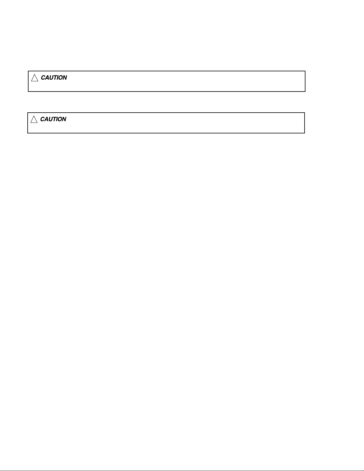
Preventing static electricity
1.Grounding to prevent damage by static electricity
Electrostatic discharge (ESD), which occurs when static electricity stored in the body, fabric, etc. is discharged,
can destroy the laser diode in the traverse unit (optical pickup). Take care to prevent this when performing repairs.
2.About the earth processing for the destruction prevention by static electricity
Static electricity in the work area can destroy the optical pickup (laser diode) in devices such as CD players.
Be careful to use proper grounding in the area where repairs are being performed.
2-1 Ground the workbench
Ground the workbench by laying conductive material (such as a conductive sheet) or an iron plate over
it before placing the traverse unit (optical pickup) on it.
2-2 Ground yourself
Use an anti-static wrist strap to release any static electricity built up in your body.
(caption)
Anti-static wrist strap
Conductive material
(conductive sheet) or iron plate
3. Handling the optical pickup
1. In order to maintain quality during transport and before installation, both sides of the laser diode on the
replacement optical pickup are shorted. After replacement, return the shorted parts to their original condition.
(Refer to the text.)
2. Do not use a tester to check the condition of the laser diode in the optical pickup. The tester's internal power
source can easily destroy the laser diode.
4.Handling the traverse unit (optical pickup)
1. Do not subject the traverse unit (optical pickup) to strong shocks, as it is a sensitive, complex unit.
2. Cut off the shorted part of the flexible cable using nippers, etc. after replacing the optical pickup. For specific
details, refer to the replacement procedure in the text. Remove the anti-static pin when replacing the traverse
unit. Be careful not to take too long a time when attaching it to the connector.
3. Handle the flexible cable carefully as it may break when subjected to strong force.
4. It is not possible to adjust the semi-fixed resistor that adjusts the laser power. Do not turn it
CD mechanism ass’y
Damper bracket
Attention when traverse unit is decomposed
*Please refer to "Disassembly method" in the text for pick-up and how to
detach the substrate.
1.Solder is put up before the card wire is removed from connector on
the CD substrate as shown in Figure.
(When the wire is removed without putting up solder, the CD pick-up
assembly might destroy.)
2.Please remove solder after connecting the card wire with
when you install picking up in the substrate.
Front bracket
Feed motor ass’y
FD screw
CD mechanism
control board
Soldering
FD gear
Pickup unit
1-3
Page 4
KD-LX300/KD-LX100
Disassembly method
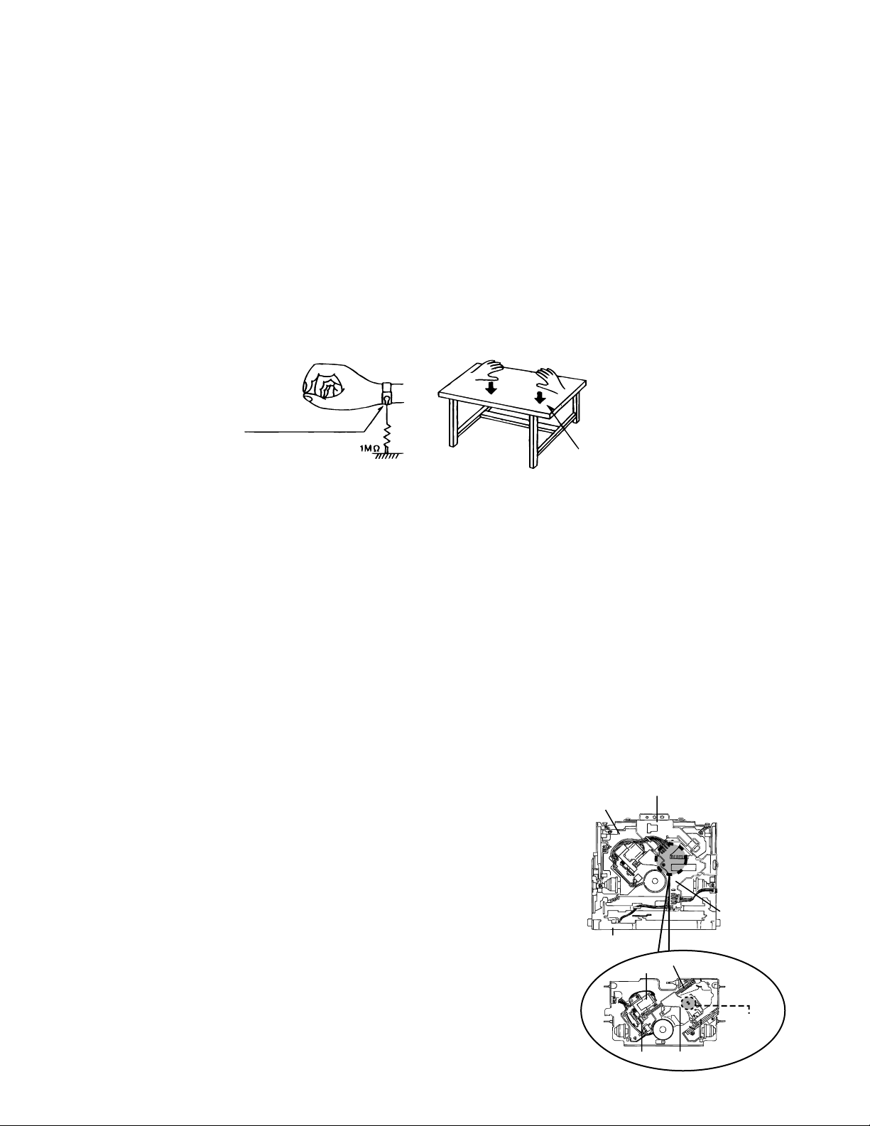
<Main body>
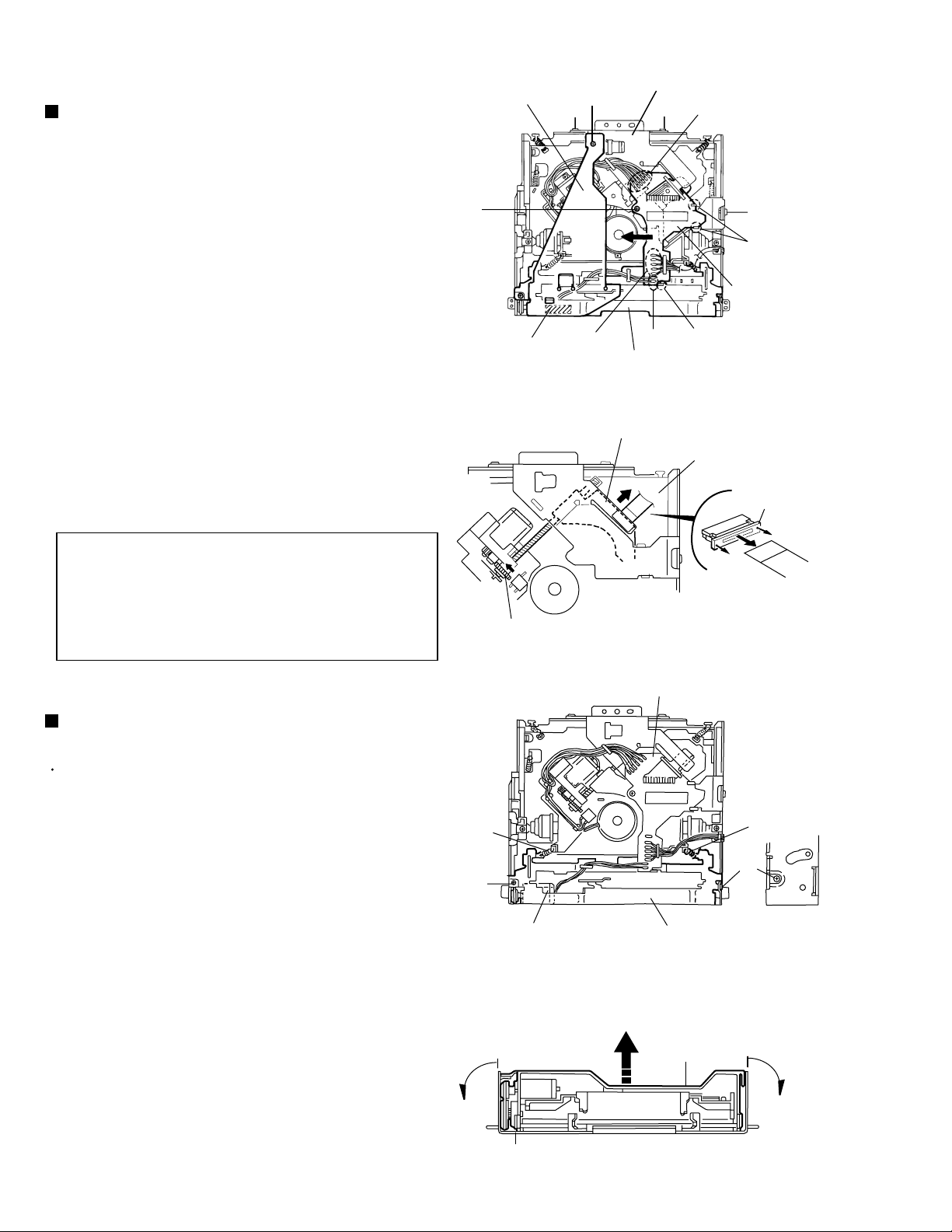
Removing the top chassis
(See Fig.1 to 5)
1.
Remove the two screws A attaching the bottom
cover to the top chassis on the bottom of the body.
2.
Remove the two screws B attaching the top chassis
on both sides of the body.
3.
Remove the two screws C and the two screw D
attaching the heat sink on the left side of the body.
4.
Remove the two screws E and the screw F on the
back of the body.
5.
Remove the two screws G on the upper side of the
body.
6.
Move the top chassis upward and disconnect the CD
mechanism connector from the main board
connector by pulling it. Remove the top chassis from
the body.
Bottom cover
A
A
Fig.1
Top chassis
B
Fig.2
E
Fig.4-1 (KD-LX300)
E
Fig.4-2 (KD-LX100)
F
F
C
Heat sink
G
Top chassis
B
D
Fig.3
Top chassis
G
1-4
Fig.5
Page 5
Removing the front panel assembly
(See Fig.6 to 8)
Prior to performing the following procedure, remove
the top chassis assembly.
1.
Disconnect the flexible harness from connector
CN701 on the main board assembly.
2.
Remove the four screws H attaching the front panel
assembly on both sides of the body. Remove the
front panel toward the front.
KD-LX300/KD-LX100
CN701
Front panel assembly
Fig.6-1 (KD-LX300)
Front panel assembly
Fig.7
H
CN701
Front panel assembly
Fig.6-2 (KD-LX100)
Front panel assembly
H
CN701
Fig.8
Removing the Front Board (See Fig.9)
Prior to performing the following procedure, remove
the top chassis assembly and the front panel
assembly.
1.
Remove the four screws I attaching the front board
on the back of the front panel assembly and release
the eight joints a.
Joints a
I
Joints a
Fig.9
I
1-5
Page 6
KD-LX300/KD-LX100
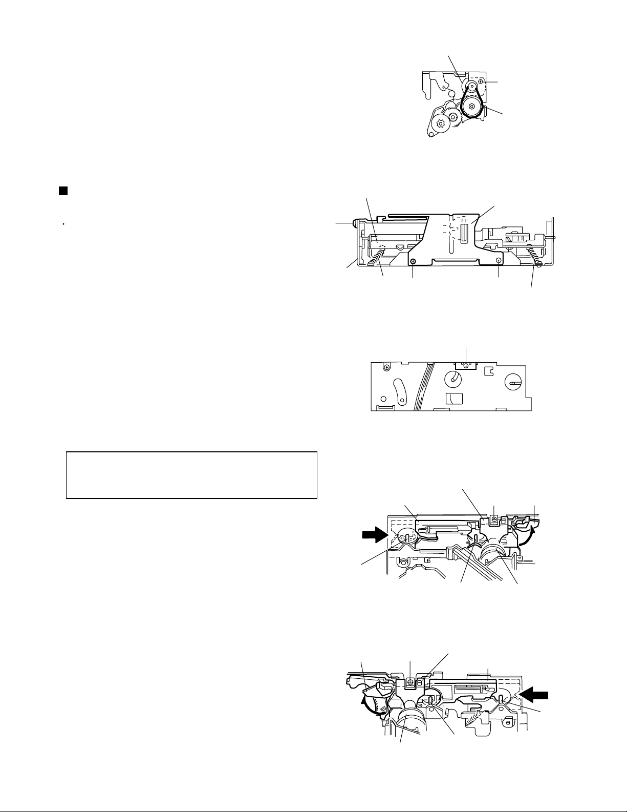
Removing the lifter unit (See Fig.10)
Prior to performing the following procedure, remove
the top chassis assembly and the front panel
assembly.
1.
Disconnect the harness from connector CN503and
CN504 on the main board.
2.
Remove the four screws J and detach the lifter unit
from the bottom cover.
Removing the feed motor (L) (See Fig.11)
Prior to performing the following procedure, remove
the lifter unit.
1.
Remove the washer attaching the clutch assembly
and detach the clutch assembly from the shaft of the
lifter unit.
2.
Remove the two screws K attaching the feed motor
(L).
CN503
J
CN504
J
Lifter unit assembly
Fig.10-1 (KD-LX300)
Removing the feed motor (R) (See Fig.12)
Prior to performing the following procedure, remove
the lifter unit.
1.
Remove the washer attaching the clutch assembly
and detach the clutch assembly from the shaft of the
lifter unit.
2.
Remove the two screws L attaching the feed motor
(R).
Clutch assembly
Lifter unit assembly
CN503
J
Clutch assembly
CN504
J
Lifter unit assembly
Fig.10-2 (KD-LX100)
Lifter unit assembly
1-6
Washer
Feed motor (R) assembly
L
Washer
Feed motor (L) assembly
K
Fig.11Fig.12
Page 7
Removing the operation assembly
(See Fig.13 to 17)
Prior to performing the following procedure, remove
the top chassis assembly, the front panel assembly
and the lifer unit.
1.
Disconnect the card wire from connector CN702 on
the main board and remove the operation assembly.
2.
Remove the three screws M attaching the right and
left brackets which fix gears on both sides of the
operation assembly.
3.
Remove the springs 5 and 6 from the operation
assembly.
ATTENTION:
When reassembling, correctly engage
the switch S651 and S652 on the
main board and the right gear with
the part b of the operation assembly.
Bracket (L)
M
Spring 5
Operation assembly
Fig.13
CN702
KD-LX300/KD-LX100
Bracket (R)
M
Spring 6
Bracket (R)
Operation assembly b
S652
S651
Operation assembly b
Fig.14
Operation assembly
b
S652
S651
Fig.15Fig.16
1-7
Page 8
KD-LX300/KD-LX100
Removing the operation switch board
(See Fig.17 and 18)
Prior to performing the following procedure, remove
the operation assembly.
1.
Remove the six screws N attaching the button panel
on the operation assembly.
2.
Pull out the operation switch board from inside of the
button panel.
Operation switch board
Button panel
N
N
Fig.17
Button panel
Removing the CD mechanism assembly
(See Fig.19)
Prior to performing the following procedure, remove
the top chassis.
1.
Remove the three screws O and the CD mechanism
assembly from the top chassis.
O
Fig.18
O
O
CD mechanism assembly
Fig.19
1-8
Page 9
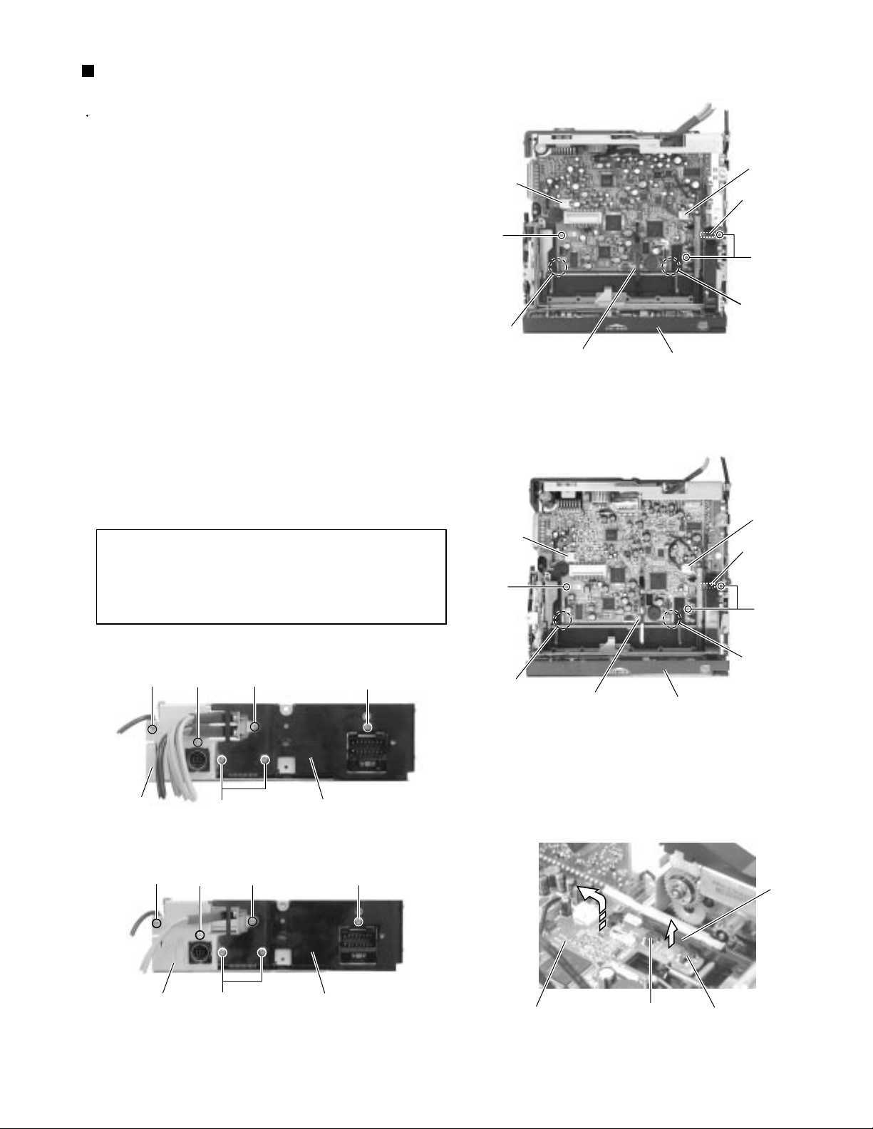
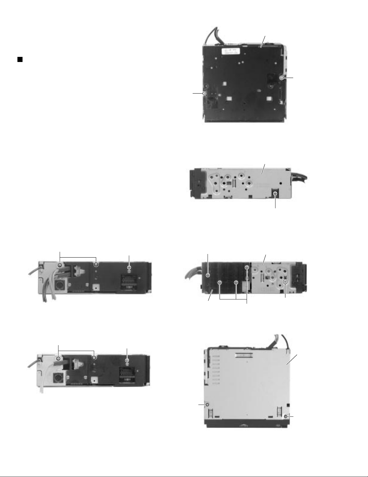
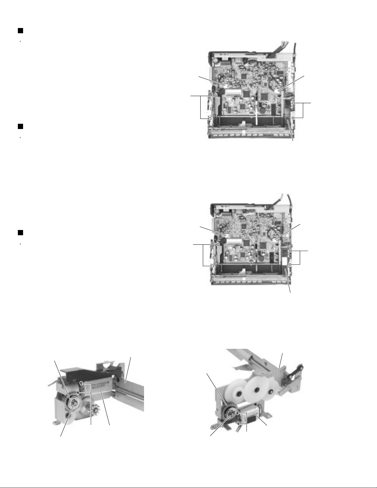
Removing the main board assembly
(See Fig.20 to 22)
Prior to performing the following procedure, remove
the top chassis.
KD-LX300/KD-LX100
1.
Disconnect the flexible harness from connector
CN701, the card wire from CN702 on the main board
and the harness from CN503 and CN504
respectively.
2.
Remove the three screws P attaching the main
board assembly to the bottom cover on the upper
side of the body.
3.
Move the main board in the direction of the arrow
and release the three joints c. (At this point, the main
board can be removed with the rear panel and the
rear heat sink.)
4.
Remove the three screws Q attaching the rear heat
sink on the back of the body.
5.
Remove the two screws R and the screw S
attaching the rear panel. Now, the main board
assembly will be removed.
ATTENTION:
When reassembling, correctly engage
the switch S651 and S652 on the
main board and the right gear with
the part b of the operation assembly
(Refer to Fig.21).
CN503
P
Joint c
CN503
P
CN702
Fig.20-1 (KD-LX300)
Front panel assembly
CN504
CN701
P
Joint c
CN504
CN701
P
Rear panel
Rear panel
R
R
S
Fig.22-1 (KD-LX300)
S
Fig.22-2 (KD-LX100)
Q
Q
R
Rear heat sink
R
Rear heat sink
Q
Q
Joint c
Main board
CN702
Fig.20-2 (KD-LX100)
Front panel assembly
S652
Fig.21
Joint c
b
S651
1-9
Page 10
KD-LX300/KD-LX100
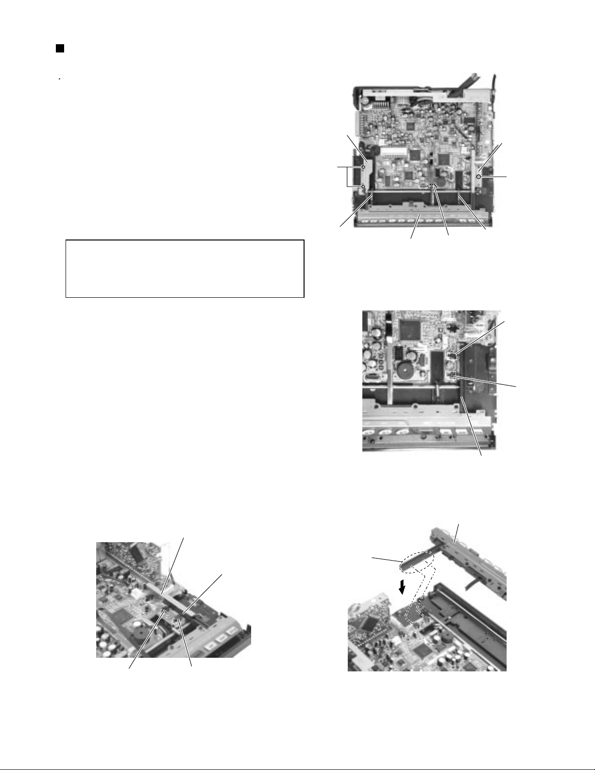
<CD mechanism section>
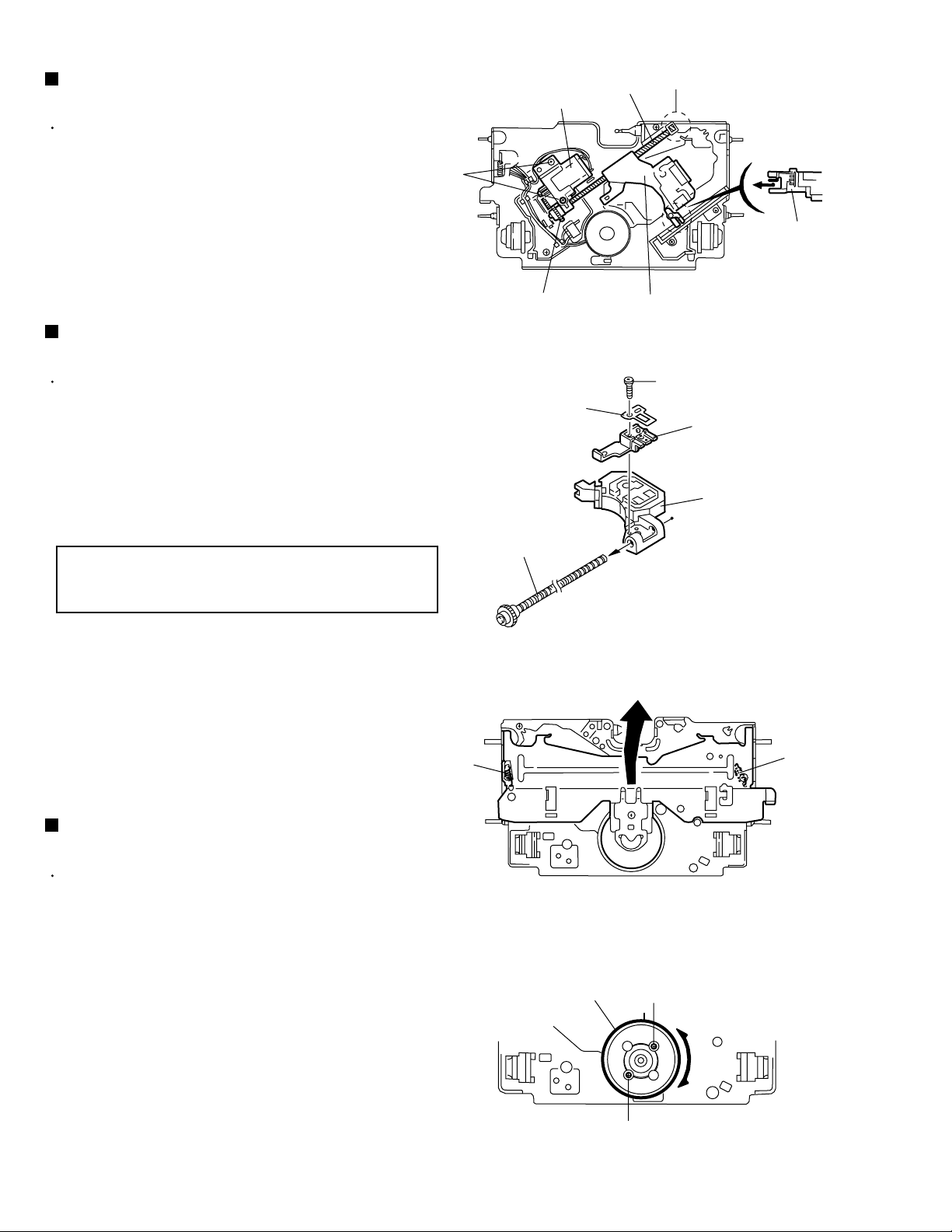
Removing the CD mechanism control
board (See Fig.1 and 2)
Remove the screw A and the pickup cover attached
1.
to the front bracket with the double-sided tapes.
Unsolder the three parts a, b and c on the CD
2.
mechanism control board.
Remove the stator fixing the CD mechanism control
3.
board and the damper bracket (To remove the stator
smoothly, pick up the center part).
Remove the screw B attaching the CD mechanism
4.
control board.
Remove the CD mechanism control board in the
5.
direction of the arrow while releasing it from the two
damper bracket slots d and the front bracket slot e.
Disconnect the flexible wire from connector on the
6.
pickup unit.
Pickup cover
B
Double-sided tape
Damper bracket
A
E
b
Front bracket
Pickup unit
c
Fig.1
E
e
Flexible wire
a
E
d
CD mechanism
control board
Shift the lock
ATTENTION:
Turn the FD gear in the direction of the
arrow to move the entire pickup unit to
the appropriate position where the
flexible wire of the CD mechanism unit
can be disconnected easily (Refer to
Fig.2).
Removing the loading motor
(See Fig.3 to 5)
Prior to performing the following procedure, remove
the CD mechanism control board and the pickup
cover.
1.
Remove the two springs f attaching the CD mechanism
assembly and the front bracket.
2.
Remove the two screws C and the front bracket
while pulling the flame outward.
3.
Remove the belt and the screw D from the loading
motor.
Spring f
C
FD gear
Loading motor
Fig.2
CD mechanism control board
Spring f
C
Front bracket
Fig.3
1-10
Pull outward
Flame
Front bracket
Fig.4
Pull outward
Page 11
Loading motor
Fig.5
KD-LX300/KD-LX100
D
Belt
Removing the CD mechanism assembly
(See Fig.1, 6 to 9)
Prior to performing the following procedure, remove
the CD mechanism control board and the front
bracket (loading motor).
1.
Remove the three screws E and the damper
bracket.
2.
Raise the both sides fix arms and move the fix plates
in the direction of the arrow to place the four shafts g
as shown in Fig.8 and 9.
3.
Remove the CD mechanism assembly and the two
springs h attaching the flame.
4.
Remove the two screws F and both sides rear
damper brackets from the dampers. Detach the CD
mechanism assembly from the left side to the right
side.
ATTENTION:
The CD mechanism assembly can be
removed if only the rear damper
bracket on the left side is removed.
CD mechanism assembly
E
Flame
Spring h
E
Fix plate (L)
Damper bracket
E
Fig.6
E
Fig.7
Rear damper bracket
F
Spring h
Fix arm (L)
Shaft g
Fix arm (R)
Damper
Shaft g
Fig.8
Rear damper bracket
F
Shaft g
Fig.9
Damper
Fix plate(R)
Shaft g
1-11
Page 12
KD-LX300/KD-LX100
Removing the feed motor assmbly
(See Fig.10)
Prior to performing the following procedure, remove
the CD mechanism control board, the front bracket
(loading motor) and the CD mechanism assembly.
1.
Remove the two screws G and the feed motor
assembly.
Removing the pickup unit
(See Fig.10 and 11)
Prior to performing the following procedure, remove
the CD mechanism control board, the front bracket
(loading motor), the CD mechanism assembly and
the feed motor assembly.
1.
Detach the FD gear part of the pickup unit upward.
Then remove the pickup unit while pulling out the
part j of the FD screw.
Feed motor assembly
G
FD gear
Nut push spring plate
FD screw
Pickup unit
Fig.10
Part j
Part i
Pickup unit
H
Pickup mount nut
Pickup unit
ATTENTION:
2.
Remove the screw H attaching the nut push spring
plate and the pickup mount nut from the pickup unit.
Pull out the FD screw.
When reattaching the pickup unit,
reattach the part i of the pickup unit,
then the part j of the FD screw.
Removing the spindle motor
(See Fig.12 and 13)
Prior to performing the following procedure, remove
the CD mechanism control board, the front bracket
(loading motor), the CD mechanism assembly and
the feed motor assembly.
1.
Turn up the CD mechanism assembly and remove
the two springs k on both sides of the clamper arms.
Open the clamper arm upward.
Spring k
FD screw
Spindle motor
Fig.11
Spring k
Fig.12
I
2.
Turn the turn table and remove the two screws I and
the spindle motor.
1-12
I
Fig.13
Page 13

Adjustment method
Test instruments required for adjustment
1. Digital oscilloscope (100MHz)
2. AM Standard signal generator
3. FM Standard signal generator
4. Stereo modulator
5. Electric voltmeter
6. Digital tester
7. Tracking offset meter
8. Test Disc JVC :CTS-1000
9. Extension cable for check
EXTGS004-26P 1
Standard measuring conditions
Power supply voltage DC14.4V(10.5~16V)
Load impedance 20Kohm(2 Speakers connection)
Output Level Line out 2.0V (Vol. MAX)
How to connect the extension cable for adjusting
Standard volume position
Balance and Bass &Treble volume : lndication"0"
Loudness : OFF
BBE : OFF
Frequency Band
FM 87.5MHz ~ 108.0MHz
MW 520kHz ~ 1620 kHz
Dummy load
Exclusive dummy load should be used for AM,and FM. For
FM dummy load,there is a loss of 6dB between SSG output
and antenna input.The loss of 6dB need not be considered
since direct reading of figures are applied in this working
standard.
KD-LX300/KD-LX100
EXTGS004-26P
EXTLX001-16PF
EXTLX002-SWPWB
EXTLX002-4P
EXTLX002-16PC
EXTLX001-2P
EXTLX001-6PC
EXTLX001-2P
EXTLX001-6PF
1-13
Page 14

KD-LX300/KD-LX100
Extension cord connecting method
Using the extention cords to connect the front panel with the main board
Remove the main board follwing the disassembly
methode. Then reattachi the heat sink to main
board.
Using the 2pin extention cord (EXTLX001-2p),
1.
connect the harness of the feed motor (L) assembly
with the connector CN503 on the main board.
Using the 2pin extention cord (EXTLX001-2p),
2.
connect the harness of the feed motor (R)
assembly with the connector CN504 on the main
board.
3.
4.
5.
Using the jig board (EXTLX002-SWPWB), its
installing to the chassis, then using 4pin extention
cord (EXTLX002-4P) connect the harness of the
lifter detecting board with the connector CN704 on
the board.
Connect the connector (EXTLX001-6PC) and
extension wire (EXTLX001-6PF), connect the 6pin
connector CN702 on the main board.
Connect the connector (EXTLX002-16PC) and
extension wire (EXTLX002-16PF), connect the
16pin connector CN701 on the main board.
EXTGS004-26P
EXTLX001-16PF
EXTLX002-SWPWB
EXTLX002-4P
EXTLX002-16PC
EXTLX001-2P
EXTLX001-6PC
EXTLX001-2P
EXTLX001-6PF
1-14
Page 15

Extension cord list
EXTLX002-JIG : Kit including the following 8 extension parts.
KD-LX300/KD-LX100
No.
1
2
3
4
5
6
7
Parts number Quantity Description
EXTLX001-2P
EXTLX001-6PF
EXTLX001-6PC
EXTLX002-16PF
EXTLX002-16PC
EXTLX002-SWPWB
EXTLX002-4P
Besides the above kit, we offer the conventional extension cord for CD mechanism
which are not essential to operation check or service. The mechanism should be
directly connected to the board using the extension wire. EXTGS004-26P
2
1
1
1
1
1
1
2Pin, 30cm extension cord
6Pin, 30cm flat wire
6Pin x 2, interlocking connector
16Pin flat wire
16Pin, interlocking connector
3 switch PWB
4Pin, 30cm extension cord
EXTGS004-26P
EXTLX001-16PF
EXTLX002-SWPWB
EXTLX002-4P
EXTLX002-16PC
EXTLX001-2P
EXTLX001-6PC
EXTLX001-2P
EXTLX001-6PF
1-15
Page 16

KD-LX300/KD-LX100
Functions of the mechanism under the service mode
With the three error modes stored in maximum in the internal memory of the mechanism in the body of this
system, it is posible under the service mode to call the contents of error according to the following steps when
any error has occurred.
Press the three buttons (UP button )+( button)+(Func button ). Then it is possible to select the follwing
service modes. After changing over to the service mode, press the UP button and DOWN button to
change the mode. For executing the respective service modes, press the SEL button.
With the service mode 2 , it is possible to call the error codes of the mechanism.
NORMAL MODE
(UP button ) + ( button) + ( button) at the same time.
DELEEPROM
CD-CH ERR
DEL CH-ERR
RUNNING
DELDATA
CD-ERR
Data stored in EEPROM
: Deletion of entire EEPROM data. This mode is used when
shipping this system from factry.
: This mode is used only when the CD changer is connected.
: This mode is used only when the CD changer is connected.
: Running mode (Do not use this mode under the servise mode)
: (Deletion of CD error code and RDS data)
: Calling of CD mechanism error code
1-16
1. RDS data
2. CD mechanism error cord
3. Station name (to be input by user)
4. DISC name (to be input by user)
5. AUX input name
*Any data 3 to 5 above should not be deleted.
UP
MODE 4
Page 17

1. Display of mechanism error
KD-LX300/KD-LX100
Error codesDescriptionOccurrence condition
Disc loading error
Eject error
Error during standby for loading
2. Display of CD error
Pickup feeding error
1. Inner peripheral feeding error
(10sec.)
2. Outer peripheral feeding error
(10sec.)
Focus search error
In the case of focusing error after
3-way focus searching
Tracking balance adjusting error
In the case of time-over (1sec.)
of timer
TOC area searching error
In the case of time-over (10sec.)
of timer
Reading error
IN the case of time-over (30sec.)
of timer
1st tracking access error
In the case of time-over (10sec.)
of timer
Last tracking access error
In the case of time-over (10sec.)
of timer
Q code reading error
In the case of time-over (0.6sec.)
of timer
TEXT data reading error
1. SW4 is not turned off.
2. SW3 is not turned on.
1. SW# is not turned off.
1. In case SW2 has been positioned to "L" before
starting loading during waiting for 15sec.
The pickup cannot returned to the inner
peripheral, and the REST switch is not turned off.
The pickup cannot be returned to the outer
peripheral, and the REST switch is not turned off.
In case the focus cannot be searched by one set
of focus searching (3-way focus searching) after
disc change and focus shock, judge that the focus
searching system is in error.
In case tracking balance cannot be adjusted even
after elapse of 1sec. following execution of the
adjusting command (TBA).
In case TOC area searching is not ended even after
elapse of 10sec.
In case reading is not ended even after elapse of 30
sec. during TOC reading action.
In case the first tracking access is not ended even
after elapse of 10sec. following completion of TOC
reading.
In case the last tracking access is not ended even
after elapse of 10sec. following completion of first
tracking under the RUNNING mode.
In case the Q code cannot be read for 0.6sec.
during playing TOC program area.
In case all TEXT data cannot be read.
09 0011
09 0013
01 0021
80 0031
Error codesDescriptionOccurrence condition
04 0051
04 0052
81 0053
82 0054
82 0055
84 0059
80 0060
80 0061
80 0062
80 0063
1-17
Page 18

KD-LX300/KD-LX100
Flow of functional operation until TOC read
Power ON
• When the pickup correctly moves
to the inner area of the disc
Set Function to CD
• When the laser diode correctly
emits
Microprocessor
commands
FMO
TC9462 "53"
FEED MOTOR
+TERMINAL
TERMINAL
IC581 "5"
REST SW
• When correctly focused
Focus Servo Loop ON
Disc inserted
Pickup feed to the inner area
Laser emitted
Focus search
Disc rotates
RF signal eye-pattern
remains closed
Tracking loop closed
RF signal eye-pattern
opens
TOC readout
YES
YES
Microprocessor
commands
"No disc"
display
• When the disc correctly rotates
Microprocessor
commands
Spindle
motor (-)
IC581 "7"
AccelerationAcceleration
0.5 Sec
Rough
Servo
0.5 Sec
Servo CLV
1-18
Jump to the first track
Play
Tracking Servo Loop ON
• RF signal
Rough Servo Mode
CLV Servo Mode
(ProgramArea)
CLV Servo Mode
(Lead-In Area;
Digital: 0)
Page 19

Feed Section
Is the voltage output at
IC521 pin "53" 5V or 0V?
YES
Is 4V present at both
sides of the feed motor?
YES
NO
Is the wiring for IC521
(90) ~ (100) correct?
NO
Is 6V or 2V present at
IC581 "5" and "6"?
NO
YES
YES
Is 5V present at IC581
pin "11"?
YES
Check the vicinity of
IC521.
Check the feed motor
connection wiring.
KD-LX300/KD-LX100
NONO
Check CD 9V
and 5V.
Check the feed motor.
Focus Section
When the lens is
moving:
4V
Does the S-search
waveform appear at
IC581 pins "17" and "18"?
Spindle Section
Is the disk rotated?
YES
Does the RF signal
appear at TP1?
YES
NO
YES
NO
Check IC581.
Check the circuits in
the vicinity of IC581
pins "15" ~ "18".
Check the pickup and
its connections.
Is 4V present at IC581
pins "7" and "8" ?
YES
Check the spindle motor
and its wiring.
NO
YES
NO NO
Is 4V present at IC521
pin "55" ?
YES
Check the vicinity of
IC581.
Check IC501 and
IC521.
Is the RF waveform at TP1
distorted?
YES
Proceed to the Tracking
section
Tracking Section
When the disc is rotated
at first:
Is the tracking error signal
output at IC501 "12"?
Check IC521.
NO
Approx. 1.2 V
YES
Check the circuits in the
vicinity of IC501 "19" ~
"24" or the pickup
Check the circuit in the
vicinity of IC501 pins
"2" ~ "12".
YESYES
Check the pickup and
its connections.
1-19
Page 20

KD-LX300/KD-LX100
Maintenance of laser pickup
(1) Cleaning the pick up lens
Before you replace the pick up, please try to
clean the lens with a alcohol soaked cotton
swab.
(2) Life of the laser diode
When the life of the laser diode has expired,
the following symptoms will appear.
(1) The level of RF output (EFM output:ampli
tude of eye pattern) will be low.
Is RF output
1.0 0.35Vp-p?
YES
O.K
(3) Semi-fixed resistor on the APC PC board
The semi-fixed resistor on the APC printed
circuit board which is attached to the pickup
is used to adjust the laser power.Since this
adjustment should be performed to match the
characteristics of the whole optical block,
do not touch the semi-fixed resistor.
If the laser power is lower than the specified
value,the laser diode is almost worn out, and
the laser pickup should be replaced.
If the semi-fixed resistor is adjusted while
the pickup is functioning normally,the laser
pickup may be damaged due to excessive current.
NO
Replace it.
Replacement of laser pickup
Turn off the power switch and,disconnect the
power cord from the ac outlet.
Replace the pickup with a normal one.(Refer
to "Pickup Removal" on the previous page)
Plug the power cord in,and turn the power on.
At this time,check that the laser emits for
about 3seconds and the objective lens moves
up and down.
Note: Do not observe the laser beam directly.
1-20
Play a disc.
Check the eye-pattern at TP1.
Finish.
Page 21

Description of major ICs
FAN8037 (IC661) : CD driver
1. Pin layout & Block diagram
48 47 46 45 44 43 42 41 40 39 38 37
1
2
3
4
5
6
KD-LX300/KD-LX100
36
35
34
33
32
31
2. Pin function
Pin
Symbol
No.
1
IN2+
2
IN2-
3
OUT2
4
IN3+
5
IN3-
6
OUT3
7
IN4+
8
IN4-
9
OUT4
10
CTL1
11
FWD1
12
REV1
13
CTL2
14
FWD2
15
REV2
16
SGND
17
FWD3
18
REV3
19
CTL3
20
SB
21
PS
22
MUTE
23
PVCC2
24
DO7-
7
8
9
10
11
12
13 14 15 16 17 18 19 20 21 22 23 24
Function
I/O
I
CH2 op-amp input(+)
I
CH2 op-amp input(-)
O
CH2 op-amp output
I
CH3 op-amp input(+)
I
Ch3 op-amp input(-)
O
CH3 op-amp output
I
CH4 op-amp input(+)
I
CH4 op-amp input(-)
O
CH4 op-amp output(+)
I
CH5 motor speed control
I
CH5 forward input
I
CH5 reverse input
I
CH6 motor speed control
I
CH6 forward input
I
CH6 reverse input
-
Signal ground
I
CH7 forward input
I
CH7 reverse input
I
CH7 motor speed control
I
Stand by
I
Power save
I
All mute
-
Power supply voltage
O
CH7 drive output(-)
M
s
S
w
C
M
s
S
w
C
M
s
S
w
C
T.S . D
D
D
D
D
D
D
STAND BY
ALL MUTE
POWER SAVE
Pin
No.
25
26
27
28
29
30
31
32
33
34
35
36
37
38
39
40
41
42
43
44
45
46
47
48
Symbol
DO7+
DO6-
DO6+
PGND2
DO5-
DO5+
DO4-
DO4+
DO3-
DO3+
PGND1
DO2-
DO2+
DO1-
DO1+
PVCC1
REGOX
REGX
RESX
VREF
SVCC
IN1+
IN1-
OUT1
30
29
28
27
26
25
Function
I/O
O
CH7 drive output(+)
O
CH6 drive output(-)
O
CH6 drive output(+)
-
Power ground2
O
CH5 drive output(-)
O
CH5 drive output(+)
O
CH4 drive output(-)
O
CH4 drive output(+)
O
CH3 drive output(-)
O
CH3 drive output(+)
-
Power ground1
O
CH2 drive output(-)
O
CH2 drive output(+)
O
CH1 drive output(-)
O
CH1 drive output(+)
-
Power supply voltage
I
Regulator feedback input
O
Regulator output
I
Regulator reset input
I
Bias voltage input
-
Signal supply voltage
I
CH1 op-amp input(+)
I
CH1 op-amp input(-)
O
CH1 op-amp output
1-21
Page 22

KD-LX300/KD-LX100
UPD784215AGC-128 (IC701) : UNIT CPU
1.Terminal Layout
75 ~ 51
76
~
50
~
100
1 ~ 25
2.Pin Function (1/2)
Pin No.
1
2
3
4
5
6
7
8
9
10
11
12
13
14
15
16
17
18
19
20
21
22
23
24
25
26
27
28
29
30
31
32
33
34
35
36
37
38
39
40
41
42
Symbol
SW2
SW3
SW4
REST-SW
LM0
LM1
DIMMER-OUT
LCD-PWR
VDD
X2
X1
VSS
XT2
XT1
RESET
SW1
BUS-INT
PS2
CRUISE
NC
NC
REMOCON
AVDD
AVREF0
VOL1
VOL2
KEY0
KEY1
KEY2
LEVEL
NC
S.METER
AVSS
W-VOL
DOT-CONT
AVREF
BUS-SI
BUS-SO
BUS-SCK
STAGE2
LCD-DA
LCDCL
26
I/O
Detection switch of CD mechanism
I
Detection switch of CD mechanism
I
Detection switch of CD mechanism
I
Reset signal input from CD mechanism
I
Loading motor control signal output
O
Loading motor control signal output
O
Dimmer signal output
O
LCD driver power supply control output H:ON
O
Power supply terminal
Connecting the crystal oscillator for system main clock
Connecting the crystal oscillator for system main clock
Power supply terminal
Connecting the crystal oscillator for system sub clock
Connecting the crystal oscillator for system sub clock
System reset signal input
I
Detection switch of CD mechanism
I
Cut-in input for J-BUS signal
I
Power save 2, Working together back up by H input, to stop mode
I
Pulse signal input port for Cruise control
I
Clock signal input for RDS
RDS data input
Remote control signal input
I
Power supply terminal
Power supply terminal
Input for rotation volume detection pulse judgment to relation V1
I
Input for rotation volume detection pulse judgment to relation V2
I
Key control signal input 0
I
Key control signal input 1
I
Key control signal input 2
I
Signal input port of level meter
I
Non connect
I
S.Meter level input
I
Connect to GND
Subwoofer volume control analogue output
O
Dot contrast signal output
O
Power supply terminal
J-BUS data input
I
J-BUS data output
O
J-BUS Clock signal I/O
I/O
Initial setting
I
Data output to LCD driver
O
Clock output to LCD driver
O
Function
1-22
Page 23

Pin Function (2/2)
KD-LX300/KD-LX100
Pin No.
43
44
45
46
47
48
49
50
51
52
53
54
55
56~60
61,62
63
64
65
66
67
68
69
70
71
72
73
74
75
76
77
78
79
80
81
82
83
84
85
86
87
88
89
90
91
92
93
94
95~98
99
100
Symbol
LCD-CE1
BUZZER
E2PR-DA-I
E2PR-DA-O
E2PR-CLK
BUS-I/O
TM0
TM1
DM0
DM1
SD/ST
LOCAL
MONO
CA-SW1~5
NC
SEEK/STOP
NC
FM/AM
PLL-CE
PLL-DA
PLL-CK
BAND IN
NC
AMP KILL
VSS
DIMMER-IN
PS1
POWER
CD-ON
MUTE
W-LPF1
W-LPF2
W-MUTE
VDD
VO-DA
VOL-CLK
NC
GVSW
LCDRST
LCD-CE2
DMK
TMK
NC
BUCK
CCE
RST
TEST
BUS0~3
DISC SEL
NC
I/O
Chip enable output to LCD driver
O
BUZZER control signal output
O
Data input terminal from EEPROM
I
Data output terminal for EEPROM
O
Clock signal I/O terminal with EEPROM
O
J-BUS I/O signal terminal
I/O
Tray motor negative signal output terminal
O
Tray motor positive signal output terminal
O
Door motor negative signal output terminal
O
Door motor positive signal output terminal
O
Station detector, Stereo signal input, H:Find Station L:Stereo
I
Local ON/OFF select signal output terminal
O
Monaural ON/OFF selecting output, H:MONO ON
O
DOOR/TRAY open close detect switch signal input terminal
I
Non connect
Auto seek/stop selecting output, H:Seek L:Stop
O
Non connect
Selecting output for FM/AM, L:FM H:AM
O
CE output for IC control for PLL
O
Data output for IC control for PLL
O
Clock output for IC control for PLL
O
AM detect signal input
I
Non connect
Non connect
Connect to GND
DIMMER signal input terminal
I
Power supply terminal
I
Selecting output for power ON/OFF, H:power ON
O
Power supply control signal for CD H:CD
O
MUTE output, L:MUTE ON
O
Subwoofer cut off frequency output 1
O
Subwoofer cut off frequency output 2
O
MUTE output for Subwoofer
O
Power supply terminal
Data output terminal
O
Clock signal output terminal
O
Non connect
AGC/FE/TE amp gain change terminal
O
LCD reset signal output terminal
O
Chip enable 2 output terminal for LCD driver
O
Motor speed control signal output terminal
O
Tray motor control signal output terminal
O
Non connect
Micon interface clock output terminal
O
Command and data sending/receiving chip enable signal output
O
Reset signal output terminal reset at "L" level
O
Connect to GND
Micon interface data input/output terminal
I/O
Initial setting
I
Non connect
-
Function
1-23
Page 24

KD-LX300/KD-LX100
TC9490FA (IC521) : DSP
1. Pin layout & Block diagram
DVss3 49
RO 50
DVDD3 51
DVR 52
LO 53
DVss3 54
ZDET 55
Vss5 56
BUS0 57
BUS1 58
BUS2 59
BUS3 60
47 XO
48 XVDD3
LPF
46 XI
Clock
generator
1-bit
DAC
45 XVss3
44 TESIN
circuit
Correction
43 VDD3
Address
circuit
16 k
RAM
42 Vss3
41 DMO
PWM
39 AVDD3
40 FMO
Servo control
ROM
RAM
CLV servo
Sync signal
protection
EFM
38 SEL
37 TEBC
Digital equalizer
automatic
adjustment circuit
36 RFGC
35 VREF
D/A
A/D
Data
slicer
VCO
34 TRO
33 FOO
32 TEZI
31 TEI
30 SBAD
29 FEI
28 RFRP
27 RFZI
26 RFCT
25 AVDD3
24 RFI
23 SLCO
22 AVss3
21 VCOF
BUCK 61
/CCE 62
/RST 63
VDD5 64
BCK 1
2. Pin function (1/2)
Pin No.
1
2
3
4
5
6
7
8
9
10
11
12
13
Symbol
BCK
LRCK
AOUT
DOUT
IPF
VDD3
Vss3
SBOK
CLCK
DATA
SFSY
SBSY
/HSO
Micro-
controller
interface
LRCK 2
I/O
O
O
O
O
O
-
O
O
O
O
O
O
Audio output
AOUT 3
circuit
DOUT 4
Digital output
IPF 5
VDD3 6
Vss3 7
CLCK 9
SBOK 8
Sub code
decoder
DATA 10
Function
Bit clock output terminal
L/R channel clock output terminal
Audio data output terminal
Digital data output terminal
Correction flag output terminal
Digital 3.3V power supply voltage terminal
Digital GND terminal
Subcode Q data CRCC result output terminal
Subcode P-W data read clock I/O terminal
Subcode P-W data output terminal
Playback frame sync signal output terminal
Subcode block sync signal output terminal
Playback speed mode output terminal
SFSY 11
SBSY 12
PLL
TMAX
/HSO 13
/UHSO 14
20 PVREF
19 LPFO
18 LPFN
17 TMAX
PDO 16
PVDD3 15
1-24
Page 25

2. Pin function (2/2)
Pin No.
14
15
16
17
18
19
20
21
22
23
24
25
26
27
28
29
30
31
32
33
34
35
36
37
38
39
40
41
42
43
44
45
46
47
48
49
50
51
52
53
54
55
56
57
58
59
60
61
62
63
64
Symbol
/UHSO
PVDD3
PDO
TMAX
LPFN
LPFO
PVREF
VCOF
AVss3
SLCO
RFI
AVDD3
RFCT
RFZI
RFRP
FEI
SBAD
TEI
TEZI
FOO
TRO
VREF
RFGC
TEBC
SEL
AVDD3
FMO
DMO
Vss3
VDD3
TESIN
XVss3
XI
XO
XVDD3
DVss3
RO
DVDD3
DVR
LO
DVss3
ZDET
Vss5
BUS0
BUS1
BUS2
BUS3
BUCK
/CCE
/RST
VDD5
I/O
Function
O
Playback speed mode output terminal
-
PLL-only 3.3V power supply voltage terminal
O
EFM and PLCK phase difference signal output terminal
O
TMAX detection result output terminal
I
Inverted input terminal for PLL LPF amp
O
Outpuit terminal for PLL LPF amp
-
PLL-only VREF terminal
O
VCO filter terminal
-
Analog GND terminal
O
DAC output terminal for data slice level generation
I
RF signal input terminal
-
Analog 3.3V power supply voltage terminal
I
RFRP signal center level input terminal
I
RFRP signal zero-cross input terminal
I
RF ripple signal input terminal
I
Focus error signal input terminal
I
Sub-beam adder signal input terminal
I
Tracking error input terminal
I
Tracking error signal zero-cross input terminal
O
Focus equalizer output terminal
O
Tracking equalizer output terminal
-
Analog reference power supply vpltage terminal
O
RF amplitude adjustment control signal output terminal
O
Tracking balance control signal output terminal
O
APC circuit ON/OFF signal output terminal
-
Analog 3.3V power supply voltage terminal
O
Feed equalizer output terminal
O
Disc equalizer output terminal
-
Digital GND terminal
-
Digital 3.3V power supply voltage terminal
I
Test input terminaal
-
System clock oscillator GND terminal
I
System clock oscillator input terminal
O
System clock oscillator output terminal
-
System clock oscillator 3.3V power supply voltage terminal
-
DA converter GND terminal
O
R-channel data forward output terminal
-
DA converter 3.3V power supply terminal
-
Reference voltage terminal
O
L-channel data forward output terminal
-
DA converter GND terminal
O
1 bit DA converter zero data detection flag output terminal
-
Microcontroller interface GND terminal
I/O
Microcontroller interface data I/O terminal
I/O
Microcontroller interface data I/O terminal
I/O
Microcontroller interface data I/O terminal
I/O
Microcontroller interface data I/O terminal
I
Microcontroller interface clock input terminal
I
Microcontroller interface chip enable signal input terminal
I
Reset signal input terminal
-
Microcontroller interface 5V power supply terminal
KD-LX300/KD-LX100
1-25
Page 26

KD-LX300/KD-LX100
BA3220FV-X (IC301,IC401) : Driver
1. Pin layout & Block diagram
CL- LGND OUTL OUTR RGND CR - CR +
1314
REFL REFR
1112 9 810
FILTER
2143675
CL+ Vcc INL NFL FIL NFR INR
2. Pin function
Pin
Symbol Function
No.
1
10
11
12
13
14
2
3
4
5
6
7
8
9
CL+
Vcc
INL
NFL
FIL
NFR
INR
CR+
CRRGND
OUTR
OUTL
LGND
CL-
Powe supply terminal for amp.
power supply terminal.
input terminal.
Negative feedback terminal.
Filter terminal.
Negative feedback terminal.
Input terminal
Power supply terminal for amp.
Output terminal of internal amp.
Rch GND terminal.
Rch output terminal.
Lch output terminal.
Lch GND terminal.
Output terminal of internal amp.
000874360-T (IC702) : System reset
1. Pin layout 2. Block diagram
13
2
1-26
1 Vcc
3 Vout
OP1
2 GND
Page 27

BD3860K (IC911) : E. volume
1.Terminal layout
33 23
KD-LX300/KD-LX100
2.Bockdiagram
GND FIL VCC SEL1
6 5 9 40 36 35 343328323130 2919 15 14
POWER
SUPPLY
A1
41
B1
42
C1
43
D1
44
INPUT
1
2
3
4
SELECTOR
A2
B2
C2
D2
34
44
1 11
INPUT
GAIN
0 18 dB
INPUT
GAIN
0 18 dB
22
12
VIN1 LOUD1 HF1 LF1 DET1 TIN1 TNF1 BNF1
MAIN
VOLUME
0 -40 dB
LOUDNESS
MAIN
VOLUME
0 -40 dB
LOUDNESS
LOW(f=50Hz) 6dB
PROCESS CONTROL +3 to 12dB
(f=10kHz)
LOGIC
LOW(f=50Hz) 6dB
PROCESS CONTROL +3 to 12dB
(f=10kHz)
TREBLE
-14 +14dB
TREBLE
-14 +14dB
-14 +14dB
-14 +14dB
BASS
BASS
BOUT1VCA1 MIX1 BBOUT1
FADER
CH1 FRONT
0 -5 dB
FADER
CH1 REAR
0 -5 dB
FADER
CH2 REAR
0 -5 dB
FADER
CH2 FRONT
0 -5 dB
13
12
10
11
7
8
OUTF1
OUTR1
SI
SC
OUTR2
OUTF2
3.Pin function
Pin
Symbol Function
No.
1
2
3
4
5
6
7
8
9
10
11
12
13
14
15
16
17
18
19
20
21
22
A2
B2
C2
D2
FIL
GND
SI
SC
VCC
OUTR2
OUTF2
OUTR1
OUTF1
BOUT1
BNF1
BOUT2
BNF2
TNF2
TNF1
TIN2
BBOUT2
MIX2
CH2 Input Pin A
CH2 Input Pin B
CH2 Input Pin C
CH2 Input Pin D
1/2 VCC Pin
Ground Pin
Serial Data Receiving Pin
Serial Clock Receiving Pin
Power Supply Pin
CH2 Rear Output Pin
CH2 Front Output Pin
CH1 Rear Output Pin
CH1 Front Output Pin
CH1 Bass Filter Setting Pin
CH1 Bass Filter Setting Pin
CH2 Bass Filter Setting Pin
CH2 Bass Filter Setting Pin
CH2 treble Filter Setting Pin
CH1 treble Filter Setting Pin
CH2 treble Input Pin
CH2 BBE II Signal Output Pin
CH2 Output MIX Amplifier
Inverse Input Pin
39 38 37 25 24 26 23 22 21 20 18 17 16
Pin
Symbol Function
No.
23
24
25
26
27
28
29
BBOUT1
30
31
32
33
34
35
36
37
38
39
40
41
42
43
44
VCA2
LF2
HF2
DET2
NC
DET1
TIN1
MIX1
VCA1
LF1
HF1
LOUD1
VIN1
LOUD2
VIN2
SEL2
SEL1
A1
B1
C1
D1
CH2 High Pass VCA Output Pin
CH2 Low Pass Filter Setting Pin
CH2 High Pass Filter Setting Pin
CH2 High Pass Attack/Release Time Setting Pin
Non connect
CH1 High Pass Attack/Release Time Setting Pin
CH1 treble Input Pin
CH1 BBE II Signal Output Pin
CH1 Output MIX Amplifier Inverse Input Pin
CH1 High Pass VCA Output Pin
CH1 Low Pass Filter Setting Pin
CH1 High Pass Filter Setting Pin
CH1 Loudness Filter Setting Pin
CH1 Main Volume Input Pin
VCH2 Loudness Filter setting Pin
CH2 Main Volume Input Pin
CH2 Input Gain Output Pin
CH1 Input Gain output Pin
CH1 Input Pin A
CH1 Input Pin B
CH1 Input Pin C
CH1 Input Pin D
BOUT2BNF2TNF2TIN2BBOUT2MIX2VCA2DET2LF2HF2LOUD2VIN2SEL2
1-27
Page 28

KD-LX300/KD-LX100
BR24C16F-X (IC703) : EEPROM
1. Pin layout
VCC WP SCL SDA
A0 A1 A2 GND
3. Block diagram
A0 1
A1 2
A2 3
11bit
Address
decoder
16kbit EEPROM allay
11bit
START
Control circuit
2. Pin function
Symbol
VCC
GND
A0,A1,A2
SCL
SDA
WP
Slave Ward
Address resister
STOP
I/O
-
Power supply.
-
GND
I
No use connect to GND.
I
Serial clock input.
I/O
Serial data I/O of slave and ward address.
I
Write protect terminal.
8bit
Data
resister
Function
8 Vcc
7 WP
6 SCL
ACK
GND 4
High voltage osc circuit
Power supply
voltage det.
BU4066BCFV-X (IC322) : Quad analog switch
1. Pin layout & Block diagram
VDD C1 C4 I/O4 I/O3O/I4 O/I3
14 13 12 11 810 9
5 SDA
1-28
1234 756
I/O1 O/I1 O/I2 I/O2 VssC2 C3
Page 29

HA13164 (IC961) : Regulator
1.Terminal layout
123456789101112131415
KD-LX300/KD-LX100
2.Block diagram
3.Pin function
ANT OUT
C3
0.1u
EXT OUT
C4
0.1u
ANT CTRL
CTRL
CD OUT
C5
0.1u
AUDIO OUT
C6
10u
11
12
10
BATT.DET OUT
9
COMPOUT
6
VDD OUT
4
SW5VOUT
5
14
UNIT R:
+B
ACC
ILMOUT
R1
C7
0.1u
C8
0.1u
C1
100u
VCC ACC
8
2
1
7
Surge Protector
BIAS TSD
15
3
note1) TAB (header of IC)
connected to GND
ILM AJGND
13
C2
0.1u
C:F
Pin No. Symbol Function
1
2
EXTOUT
ANTOUT
Output voltage is VCC-1 V when M or H level applied to CTRL pin.
Output voltage is VCC-1 V when M or H level to CTRL pin and H level
to ANT-CTRL.
3
4
5
6
7
8
9
10
11
12
13
14
15
ACCIN
VDDOUT
SW5VOUT
COMPOUT
ANT CTRL
VCC
BATT DET
AUDIO OUT
CTRL
CD OUT
ILM AJ
ILM OUT
GND
Connected to ACC.
Regular 5.7V.
Output voltage is 5V when M or H level applies to CTRL pin.
Output for ACC detector.
L:ANT output OFF , H:ANT output ON
Connected to VCC.
Low battery detect.
Output voltage is 9V when M or H level applied to CTRL pin.
L:BIAS OFF, M:BIAS ON, H:CD ON
Output voltage is 8V when H level applied to CTRL pin.
Adjustment pin for ILM output voltage.
Output voltage is 10V when M or H level applies to CTRL pin.
Connected to GND.
1-29
Page 30

KD-LX300/KD-LX100
HD74HC126FP (IC771) : Changer control
OE1
OE2
A1
Y1
A2
Y2
Vss
1
2
3
4
5
6
7
HD74HC126
14
13
12
11
10
Vcc
OE4
A4
Y4
OE3
A3
9
Y3
8
NJM2100M (IC821) : Operation amp
A OUT
A IN–
A IN+
VEE
1
A
+ –
2
B
+ –
3
4
8
7
6
5
VCC
B OUT
B IN–
B IN+
M5282FP-XE (IC321) : E. volume
1. Pin layout
1
2
3
4
5
3. Pin function
Pin
Symbol Function
No.
1
Vcc/2
2
Amp+IN
3
Amp-IN
4
Amp OUT
5
GND
6
7
VCA IN
8
9
VCA OUT
10
NC
Vc
Vcc
10
9
8
7
6
Vcc/2 output for microphone amp.
Microphone amp. positive input terminal.
Microphone amp. negative input terminal.
Microphone amp. output terminal.
Ground.
Non connection.
VCA input terminal.
VCA control terminal.
VCA output terminal.
Power supply.
2. Block diagram
1
2
3
10
457
9
8
1-30
Page 31

LA4743K (IC941) : Power amp
1.Block diagram
KD-LX300/KD-LX100
OUT 1+
9
+
20
Vcc 3/4
-
6
Vcc 1/2
11
IN 1
2.Terminal layout
OUT 1-
7
-
+
1
TA B
PWR GND1
OUT 2+
8
+
circuit
Protective
OUT 2-
5
3
-
-
+
12
IN 2
PWR GND2
2
Switch
Stand by
4
ST BY
Mute
22
Mute
Ripple
10
R.F
circuit
Filter
OUT 3+
17
+
-
15
IN 3
OUT 3-
19
-
+
Protective
25
N.C
PWR GND3
18
OUT 4+
21
+
circuit
-
13
PRE GND
OUT 4-
23
-
+
14
IN 4
PWR GND4
24
Circuit
Muting &
ON Time Control
16
ON TIME C
3.Pin function
1
2
3
4
5
6
7
8
9
10
11
12
13
14
15
16
17
18
19
20
21
22
23
24
25
SymbolPin No. Function
TA B
GND
OUTRRSTBY
OUTRR+
VCC1/2
OUTRFGND
OUTRF+
RIPPLE
INRF
INRR
SGND
INLR
INLF
ONTIME
OUTLF+
GND
OUTLFVCC3/4
OUTLR+
MUTE
OUTLRGND
NC
Header of IC
Power GND
Outpur(-) for front Rch
Stand by input
Output (+) for front Rch
Power input
Output (-) for rear Rch
Power GND
Output (+) for rear Rch
Ripple filter
Rear Rch input
Front Rch input
Signal GND
Front Lch input
Rear Lch input
Power on time control
Output (+) for rear Lch
Power GND
Output (-) for rear Lch
Power input
Output (+) for front
Muting control input
Output (-) for front
Power GND
Non connection
1-31
Page 32

KD-LX300/KD-LX100
LC75811W (IC602) : LCD driver
1. Pin layout
60 ~ 41
61
40
2. Block diagram
VDD
VLCD
VLCD1
VLCD2
VLCD3
VSS
RES
~
80
COM1
COMMON
DRIVER
1 ~ 20
COM8
TIMING
GENERATOR
CLOCK
GENERATOR
21
~
S60/COM9
S59/COM10
S58
INSTRUCTION
DECODER
INSTRUCTION
REGISTER
SEGMENT DRIVER
LATCH
ADRAM
60
bits
ADDRESS
COUNTER
ADDRESS
REGISTER
SHIFT REGISTER
CGRAM
5x9x16
bits
DCRAM
48x8
bits
CCB INTERFACE
S1
CGROM
5x9x240
bits
3. Pin function
1-32
Pin No.
1~58
59
60~65
66
67
68
69~71
72
73
74
75
76
77
78
79~80
OSCI
OSCO
Symbol I/O Function
O
S3~S60
COM0
COM3~COM8
COM1
VDD
VLCD
VLCD1~VLCD3
VSS
OSCO
OSCI
RES
CE
CL
DI
S1~S2
Segment driver output terminal
O
Common driver output terminal
O
Common driver output terminal
O
Common driver output terminal
-
Power supply for logic section
-
Power supply for LCD driver section
I
LCD voltage input terminal
-
Connect to ground
O
Oscillation output terminal
I
Oscillation input terminal
I
Reset signal input terminal
I
Chip enable input terminal
I
Clock signal input terminal
I
Serial data input terminal
O
Segmrnt driver output terminal
DI
CL
CE
Page 33

LC75823W (IC602) : LCD driver
1. Pin Layout & Symbol
KD-LX300/KD-LX100
S1
S2
S3
S4
S5
S6
S7
S8
S9
S10
S11
S12
S13
S14
S15
S16
2. Pin Function
Pin No.
1 to 52
53 to 55
S1 to S52
COM1 to COM3
56
57
58
59
60
61
62
63
DICLCE
64 63 62 61 60 59 58 57 56 55 54 53 52 51 50 49
1
2
3
4
5
6
7
8
9
10
11
12
13
14
15
16
17 18 19 20 21 22 23 24 25 26 27 28 29 30 31 32
S17
Symbol
S18
OSC
Vss
VDD2
VDD1
INH
VDD
COM3
COM2
S19
S20
S21
S22
S23
S24
S25
S26
S27
I/O
O
Segment output pins used to display data transferred
by serial data input.
O
Common driver output pins. The frame frequency is given
by : t0=(fosc/384)Hz.
--
VDD
Power supply connection. Provide a voltage of between
4.5 and 6.0V.
I
INH
Display turning off input pin.
INT="L" (Vss) ----- off (S1 to S52, COM1 to COM3="L"
INT="H" (VDD)----- on
Serial data can be transferred in display off mode.
I
VDD1
Used for applying the LCD drive 2/3 bias voltage
externally.
Must be connected to VDD2 when a 1/2 bias drive scheme
is used.
I
VDD2
Used for applying the LCD drive 1/3 bias voltage
externally.
Must be connected to VDD1 when a 1/2 bias drive scheme
is used.
--
Vss
OSC
Power supply connection. Connect to GND.
I/O
Oscillator connection.
An oscillator circuit is formed by connecting an external
resistor and capacitor at this pin.
CE
Serial data CE : Chip enable
interface connection
I
CL
to the controller. CL : Sync clock
COM1
S52
S28
S29
Function
S51
S30
S50
S31
S49
48
47
46
45
44
43
42
41
40
39
38
37
36
35
34
33
S32
S48
S47
S46
S45
S44
S43
S42
S41
S40
S39
S38
S37
S36
S35
S34
S33
64
DI
DI : Transfer data
1-33
Page 34

KD-LX300/KD-LX100
NJM2904M (IC951) : Dual ope amp
1. Pin layout
A OUT 1
A -IN 2
A +IN 3
GND 4
8 V+
7 B OUT
6 B -IN
5 B +IN
RPM6938-SV4 (IC603) : Remote censor
1.Block diagram
AMP
I/V
conversion
BPF
AGC
NJM4565MD (IC323,IC960) : Ope amp
1. Pin layout & Block diagram
A OUTPUT 1
A - INPUT 2
A + INPUT 3
V- 4
Vcc
Comp
Detector
22k
8 V+
BA
7 B OUTPUT
6 B - INPUT
5 B + INPUT
Vcc
Rout
PD
magnetic shield
fo
trimming
circuit
GND
1-34
Page 35

KD-LX300/KD-LX100
TA2147F-X (IC601) : Head amp
30 k
80 k
AGCIN 21
20 k
15 pF
1
x0.5
x2
240 k
1. Pin layout & Block diagram
GND 24
3 k
RFN 23
3 k
40 pF
20 k
180 k
60 k
80 k
RFO 22
180 k
40 pF
60 k
20 k
RFGC 20
15 pF
k
x0.5
x2
240 k
1.75 k
RFGO 19
40 k
14 k
2 k
RFRPIN 18
20 k
BOTTOM
PEAK
12 k
1.3V
60 A
1 k
RFRP 17
20 k
12 k
2 k
50 k
FEN 16
10 pF
50 A
40 k
FEO 15
15 k
20 k
20 k
10 pF
20 k
40 k
VRO 14
20 A
GVSW 13
20 k 20 k
PEAK
50 k
15 k
1 Vcc
2. Pin function
Pin No.
Symbol
1
2
3
4
5
6
7
8
9
10
11
12
13
14
15
16
17
18
19
20
21
22
23
24
MDI
LDO
SEL
TEBC
TEN
TEO
RFDC
GVSW
VRO
FEO
FEN
RFRP
RFRPIN
RFGO
RFGC
AGCIN
RFO
RFN
GND
Vcc
FIN
FPI
TPI
TNI
2 FNI
3 FPI
I/O
I
I
I
I
I
O
I
4 TPI
5 TNI
Function
3.3V power supply terminal
Main-beam amp input terminal
Main-beam amp input terminal
Sub-beam amp input terminal
Sub-beam amp input terminal
Monitor photo diode amp input terminal
Laser diode amp output terminal
APC circuit ON/OFF control signmal, laser diode (LDO) control signal input or
6 MDI
7 LDO
8 SEL
9 REBC
10 TEN
11 TEO
bottom/peak detection frequency change terminal
I
Tracking error balance adjustment signal input terminal
I
Tracking error signal generation amp negative-phase input terminal
O
Tracking error signal generation amp output terminal
O
RF signal peak detection output terminal
I
AGC/FE/TE amp gain change terminal
O
Reference voltage (VRO) output terminal
O
Focus error signal generation amp output terminal
I
Focus error signal generation amp negative-phase input terminal
O
Signal amp output pin for track count
I
Signal generation amp input terminal for track count
O
RF signal amplitude adjustment amp output terminal
I
RF amplitude adjustment control signal input terminal
I
RF signal amplitude adjustment amp input terminal
O
RF signal generation amp output terminal
I
RF signal generation amp input terminal
-
GND terminal
12 RFDC
1-35
Page 36

KD-LX300/KD-LX100
TA8273H (IC941) : 4ch amp
1. Pin layout 2. Block diagram
1
TA B
11
125
12
16
IN1
IN2
AUX IN
20 6
Vcc1 Vcc2
OUT1 (+)
PW-GND1
OUT1 (-)
OUT2 (+)
PW-GND2
OUT2 (-)
9
8
7
5
2
3
15
14
13
IN3
IN4
DIAGNOSIS
RIP STBY MUTE
10
4
OUT
25
OUT3 (+)
PW-GND3
OUT3 (-)
OUT4 (+)
PW-GND4
OUT4 (-)
22
17
18
19
21
24
23
1-36
Page 37

TB2118F-X (IC21) : PLL
1.Terminal Layout
2423222120191817161514
KD-LX300/KD-LX100
13
2.Block diagram
osc
2
1
XO
24
XI
FM VCO
AMVCO
IFC
CE
DIN
DOUT
DIMM
15
16
13
3
4
5
6
123456789
Buff.
ON/OFF
OSC circuit
AMP
AMP
AMP
Serial
Interface
101112
Reference Counter
Prescaler
20-bit BINARY COUNTER
Resistor 1
Resistor 2
I/O PORT
Swallow counter
Phase
Comparator
4-bit
12-bit
Programmable counter
22-bit
40bit shift register
OUTPUT PORT
Constant
power supply voltage
switch
Vdd
switch
Vcc
AM CP.
20
+
+
-
REG.
22
19
vt
18
FM cp
3.Pin Function
Pin
Symbol I/O Function
No.
XOUT
10
11
12
1
2
3
4
5
6
7
8
9
OSC
CE
DI
CK
DOUT
SR
I/01
I/02
OUT1
OUT2
VDD2
Crystal oscillator pin
O
Non connect
Chip enable input
I
Serial data input
I
Clock input
I
Serial data output
O
Register control pin
O
I/O ports
I/O
I/O ports
I/O
Non connect
Non connect
Single power supply for REF. frequency block
-
7
SL
8
9
I/O -2I/O -1
10 11
12
out-2out-1
vdd2
Pin
Symbol I/O Function
No.
IFC
13
VDD
14
FMIN
15
AMIN
16
DGND
17
FMCP
18
VT
19
AMCP
20
VCC
21
RF
22
AGND
23
XIN
24
17
14
IF signal input
I
Power pins for digital block
FM band local signal input
I
AM band local signal input
I
Connect to GND (for digital circuit)
Charge pump output for FM
O
Tuning voltage biased to 2.5V.
Charge pump output for AM
O
Power pins for analog block
Ripple filter connecting pin
I
Connect to GND (for analog circuit)
Crystal oscillator pin
I
21
23
a-gnd
vccd-gndvdd
1-37
Page 38

KD-LX300/KD-LX100
VICTOR COMPANY OF JAPAN, LIMITED
MOBILE ELECTRONICS DIVISION
PERSONAL & MOBILE NETWORK BUSINESS UNIT. 10-1,1Chome,Ohwatari-machi,Maebashi-city,371-8543,Japan
(No.49635)
200104
 Loading...