

Page 1

This file was downloaded and provided FREE OF CHARGE
from the ManualDirectory community.
You can find many free to download Service Manuals & Schematics at
http://www.manualdirectory.co.uk
Page 2
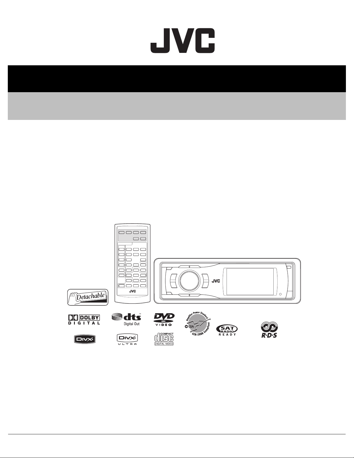
MA30420073SERVICE MANUALEXAD
SERVICE MANUAL
DVD/CD RECEIVER
KD-AVX11J,KD-AVX11E,
KD-AVX11EU,KD-AVX11EE,
KD-AVX11U,KD-AVX11UN,
KD-AVX11UT,KD-AVX11A
for Europefor Northern America
COPYRIGHT © 2007 Victor Company of Japan, Limited
Lead free solder used in the board (material : Sn-Ag-Cu, melting point : 219 Centigrade)
Lead free solder used in the board (material : Sn-Cu, melting point : 230 Centigrade)
TABLE OF CONTENTS
1 PRECAUTION. . . . . . . . . . . . . . . . . . . . . . . . . . . . . . . . . . . . . . . . . . . . . . . . . . . . . . . . . . . . . . . . . . . . . . . . . 1-6
2 SPECIFIC SERVICE INSTRUCTIONS . . . . . . . . . . . . . . . . . . . . . . . . . . . . . . . . . . . . . . . . . . . . . . . . . . . . . . 1-9
3 DISASSEMBLY . . . . . . . . . . . . . . . . . . . . . . . . . . . . . . . . . . . . . . . . . . . . . . . . . . . . . . . . . . . . . . . . . . . . . . 1-10
4 ADJUSTMENT . . . . . . . . . . . . . . . . . . . . . . . . . . . . . . . . . . . . . . . . . . . . . . . . . . . . . . . . . . . . . . . . . . . . . . . 1-24
5 TROUBLESHOOTING . . . . . . . . . . . . . . . . . . . . . . . . . . . . . . . . . . . . . . . . . . . . . . . . . . . . . . . . . . . . . . . . . 1-37
COPYRIGHT © 2007 Victor Company of Japan, Limited
No.MA304
2007/3
Page 3

SPECIFICATION
For Northern America
AMPLIFIER
Power Output 20 W RMS × 4 Channels at 4 Ω and [< or =] 1% THD+N
Signal-to-Noise Ratio 70 dB (reference: 1 W into 4 Ω)
Load Impedance 4 Ω (4 Ω to 8 Ω allowance)
Equalizer Control Range Frequencies 60 Hz, 150 Hz, 400 Hz, 1 kHz, 2.5 kHz, 6.3 kHz, 15 kHz
Level ±10 dB
Audio Output Level
LINE OUT(FRONT/REAR)/
SUBWOOFER
Color System NTSC
Video Output (composite) 1 Vp-p/75 Ω
Other Terminals Input LINE IN, VIDEO IN, Antenna input
Frequency Range FM (with channel interval set to 100 kHz or 200 kHz) 87.5 MHz to 107.9 MHz
FM Tuner Usable Sensitivity 11.3 dBf (1.0 µV/75 Ω)
AM Tuner Sensitivity/Selectivity 20 µV/35 dB
Signal Detection System Non-contact optical pickup (semiconductor laser)
Frequency Response DVD, fs=48 kHz 16 Hz to 22 000 Hz
Dynamic Range 93 dB
Signal-to-Noise Ratio 95 dB
Wow and Flutter Less than measurable limit
Screen Size 2.7 inch wide liquid crystal display
Number of Pixel 123 200 pixels: 560 (horizontal) × 220 (vertical)
Drive Method TFT (Thin Film Transistor) active matrix format
Color System PAL/NTSC
Aspect Ratio 16:9 (wide)
Allowable Storage Temperature -10°C to +60°C (14°F to 140°F)
Allowable Operating Temperature 0°C to +40°C (32°F to 104°F)
Power Requirement Operating Voltage DC 14.4 V (11 V to 16 V allowance)
Grounding System Negative ground
Allowable Operating Temperature 0°C to +40°C (32°F to 104°F)
Dimensions (W × H × D) Installation Size (approx.) 182 mm × 52 mm × 160 mm (7-3/16" × 2-1/16" × 6-5/16")
Mass (approx.) 2.1 kg (4.7 lbs) (excluding accessories)
Design and specifications are subject to change without notice.
Line-Out Level/Impedance 2.5 V/20 kΩ load (full scale)
Output Impedance 1 kΩ
Output VIDEO OUT, DIGITAL OUT (optical)
Others CD changer, OE REMOTE
FM/AM TUNER
FM (with channel interval set to 50 kHz) 87.5 MHz to 108.0 MHz
AM (with channel interval set to 10 kHz) 530 kHz to 1 710 kHz
AM (with channel interval set to 9 kHz) 531 kHz to 1 602 kHz
50 dB Quieting Sensitivity 16.3 dBf (1.8 µV/75 Ω)
Alternate Channel Selectivity (400 kHz) 65 dB
Frequency Response 40 Hz to 15 000 Hz
Stereo Separation 35 dB
DVD/CD
DVD, fs=96 kHz 16 Hz to 22 000 Hz
VCD/CD 16 Hz to 20 000 Hz
MONITOR
GENERAL
Panel Size (approx.) 188 mm × 58 mm × 14 mm (7-7/16" × 2-5/16" × 5/8")
1-2 (No.MA304)
Page 4
For Europe
AMPLIFIER
Maximum Power Output Front/Rear 50 W per channel
Continuous Power Output (RMS) Front/Rear 20 W per channel into 4 Ω, 40 Hz to 20 000 Hz at no more
than 0.8% total harmonic distortion
Load Impedance 4 Ω (4 Ω to 8 Ω allowance)
Equalizer Control Range Frequencies 60 Hz, 150 Hz, 400 Hz, 1 kHz, 2.5 kHz, 6.3 kHz, 15 kHz
Level ±10 dB
Signal-to-Noise Ratio 70 dB
Audio Output Level
LINE OUT(FRONT/REAR)/
SUBWOOFER
Color System PAL
Video Output (composite) 1 Vp-p/75 Ω
Other Terminals Input LINE IN, VIDEO IN, Aerial input
Frequency Range FM 87.5 MHz to 108.0 MHz
FM Tuner Usable Sensitivity (LW) 144 kHz to 279 kHz
MW Tuner Sensitivity/Selectivity 35 dB
LW Tuner Sensitivity 20 µV/35 dB
Signal Detection System Non-contact optical pickup (semiconductor laser)
Frequency Response DVD, fs=48 kHz 16 Hz to 22 000 Hz
Dynamic Range 93 dB
Signal-to-Noise Ratio 95 dB
Wow and Flutter Less than measurable limit
Screen Size 2.7 inch wide liquid crystal display
Number of Pixel 123 200 pixels: 560 (horizontal) × 220 (vertical)
Drive Method TFT (Thin Film Transistor) active matrix format
Color System PAL/NTSC
Aspect Ratio 16:9 (wide)
Allowable Storage Temperature -10°C to +60°C
Allowable Operating Temperature 0°C to +40°C
Power Requirement Operating Voltage DC 14.4 V (11 V to 16 V allowance)
Grounding System Negative ground
Allowable Operating Temperature 0°C to +40°C
Dimensions (W × H × D) Installation Size (approx.) 182 mm × 52 mm × 160 mm
Mass (approx.) 2.1 kg (excluding accessories)
Line-Out Level/Impedance 2.5 V/20 kΩ load (full scale)
Output Impedance 1 kΩ
Output VIDEO OUT, DIGITAL OUT (optical)
Others CD changer, OE REMOTE
FM/AM TUNER
AM (MW) 522 kHz to 1 620 kHz
50 dB Quieting Sensitivity 11.3 dBf (1.0 µV/75 Ω)
Alternate Channel Selectivity (400 kHz) 16.3 dBf (1.8 µV/75 Ω)
Frequency Response 65 dB
Stereo Separation 40 Hz to 15 000 Hz
DVD/CD
DVD, fs=96 kHz 16 Hz to 22 000 Hz
VCD/CD 16 Hz to 20 000 Hz
MONITOR
GENERAL
Panel Size (approx.) 188 mm × 58 mm × 14 mm
Design and specifications are subject to change without notice.
(No.MA304)1-3
Page 5

For Eastern Europe
AMPLIFIER
Maximum Power Output Front/Rear 50 W per channel
Continuous Power Output (RMS) Front/Rear 20 W per channel into 4 Ω, 40 Hz to 20 000 Hz at no more
than 0.8% total harmonic distortion
Load Impedance 4 Ω (4 Ω to 8 Ω allowance)
Equalizer Control Range Frequencies 60 Hz, 150 Hz, 400 Hz, 1 kHz, 2.5 kHz, 6.3 kHz, 15 kHz
Level ±10 dB
Signal-to-Noise Ratio 70 dB
Audio Output Level
LINE OUT(FRONT/REAR)/
SUBWOOFER
Color System PAL
Video Output (composite) 1 Vp-p/75 Ω
Other Terminals Input LINE IN, VIDEO IN, Aerial input
Frequency Range FM 87.5 MHz to 108.0 MHz
FM Tuner Usable Sensitivity 11.3 dBf (1.0 µV/75 Ω)
MW Tuner Sensitivity/Selectivity 20 µV/35 dB
LW Tuner Sensitivity 50 µV
Signal Detection System Non-contact optical pickup (semiconductor laser)
Frequency Response DVD, fs=48 kHz 16 Hz to 22 000 Hz
Dynamic Range 93 dB
Signal-to-Noise Ratio 95 dB
Wow and Flutter Less than measurable limit
Screen Size 2.7 inch wide liquid crystal display
Number of Pixel 123 200 pixels: 560 (horizontal) × 220 (vertical)
Drive Method TFT (Thin Film Transistor) active matrix format
Color System PAL/NTSC
Aspect Ratio 16:9 (wide)
Allowable Storage Temperature -10°C to +60°C
Allowable Operating Temperature 0°C to +40°C
Power Requirement Operating Voltage DC 14.4 V (11 V to 16 V allowance)
Grounding System Negative ground
Allowable Operating Temperature 0°C to +40°C
Dimensions (W × H × D) Installation Size (approx.) 182 mm × 52 mm × 160 mm
Mass (approx.) 2.1 kg (excluding accessories)
Line-Out Level/Impedance 2.5 V/20 kΩ load (full scale)
Output Impedance 1 kΩ
Output VIDEO OUT, DIGITAL OUT (optical)
Others CD changer, OE REMOTE
FM/AM TUNER
AM (MW) 522 kHz to 1 620 kHz
(LW) 144 kHz to 279 kHz
50 dB Quieting Sensitivity 16.3 dBf (1.8 µV/75 Ω)
Alternate Channel Selectivity (400 kHz) 65 dB
Frequency Response 40 Hz to 15 000 Hz
Stereo Separation 35 dB
DVD/CD
DVD, fs=96 kHz 16 Hz to 22 000 Hz
VCD/CD 16 Hz to 20 000 Hz
MONITOR
GENERAL
Panel Size (approx.) 188 mm × 58 mm × 14 mm
Design and specifications are subject to change without notice.
1-4 (No.MA304)
Page 6
For Asia and Australia
AMPLIFIER
Maximum Power Output Front/Rear 50 W per channel
Continuous Power Output Front/Rear 20 W per channel into 4 Ω, 40 Hz to 20 000 Hz at no more
than 0.8% total harmonic distortion.
Load Impedance 4 Ω (4 Ω to 8 Ω allowance)
Equalizer Control Range Frequencies 60 Hz, 150 Hz, 400 Hz, 1 kHz, 2.5 kHz, 6.3 kHz, 15 kHz
Level ±10 dB
Signal-to-Noise Ratio 70 dB
Audio Output Level
LINE OUT(FRONT/REAR)/
SUBWOOFER
Color System NTSC/PAL
Video Output (composite) 1 Vp-p/75 Ω
Other Terminals Input LINE IN, VIDEO IN, Antenna input
Frequency Range FM 87.5 MHz to 108.0 MHz
FM Tuner Usable Sensitivity 11.3 dBf (1.0 µV/75 Ω)
AM Tuner Sensitivity/Selectivity 20 µV/35 dB
Signal Detection System Non-contact optical pickup (semiconductor laser)
Frequency Response DVD, fs=48 kHz 16 Hz to 22 000 Hz
Dynamic Range 93 dB
Signal-to-Noise Ratio 95 dB
Wow and Flutter Less than measurable limit
Screen Size 2.7 inch wide liquid crystal display
Number of Pixel 123 200 pixels: 560 (horizontal) × 220 (vertical)
Drive Method TFT (Thin Film Transistor) active matrix format
Color System NTSC/PAL
Aspect Ratio 16:9 (wide)
Allowable Storage Temperature -10°C to +60°C
Allowable Operating Temperature 0°C to +40°C
Power Requirement Operating Voltage DC 14.4 V (11 V to 16 V allowance)
Grounding System Negative ground
Allowable Operating Temperature 0°C to +40°C
Dimensions (W × H × D) Installation Size (approx.) 182 mm × 52 mm × 160 mm
Mass (approx.) 2.1 kg (excluding accessories)
Line-Out Level/Impedance 2.5 V/20 kΩ load (full scale)
Output Impedance 1 kΩ
Output VIDEO OUT, DIGITAL OUT (optical)
Others: CD changer
FM/AM TUNER
AM 531 kHz to 1 602 kHz
50 dB Quieting Sensitivity 16.3 dBf (1.8 µV/75 Ω)
Alternate Channel Selectivity (400 kHz) 65 dB
Frequency Response 40 Hz to 15 000 Hz
Stereo Separation 35 dB
DVD/CD
DVD, fs=96 kHz 16 Hz to 22 000 Hz
VCD/CD 16 Hz to 20 000 Hz
MONITOR
GENERAL
Panel Size (approx.) 188 mm × 58 mm × 14 mm
Design and specifications are subject to change without notice.
(No.MA304)1-5
Page 7
1.1 Safety Precautions
SECTION 1
PRECAUTION
!
!
Burrs formed during molding may be left over on some parts of the chassis. Therefore,
pay attention to such burrs in the case of preforming repair of this system.
Please use enough caution not to see the beam directly or touch it in case of an
adjustment or operation check.
1-6 (No.MA304)
Page 8
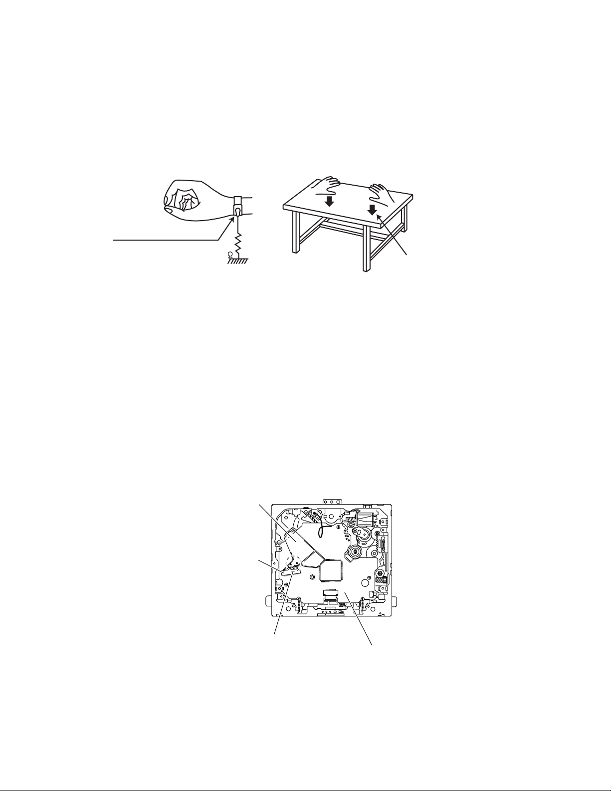
1.2 Preventing static electricity
Electrostatic discharge (ESD), which occurs when static electricity stored in the body, fabric, etc. is discharged, can destroy the laser
diode in the traverse unit (optical pickup). Take care to prevent this when performing repairs.
1.2.1 Grounding to prevent damage by static electricity
Static electricity in the work area can destroy the optical pickup (laser diode) in devices such as laser products.
Be careful to use proper grounding in the area where repairs are being performed.
(1) Ground the workbench
Ground the workbench by laying conductive material (such as a conductive sheet) or an iron plate over it before placing the
traverse unit (optical pickup) on it.
(2) Ground yourself
Use an anti-static wrist strap to release any static electricity built up in your body.
(caption)
Anti-static wrist strap
1M
Conductive material
(conductive sheet) or iron plate
(3) Handling the optical pickup
• In order to maintain quality during transport and before installation, both sides of the laser diode on the replacement optical
pickup are shorted. After replacement, return the shorted parts to their original condition.
(Refer to the text.)
• Do not use a tester to check the condition of the laser diode in the optical pickup. The tester's internal power source can easily
destroy the laser diode.
1.3 Handling the traverse unit (optical pickup)
(1) Do not subject the traverse unit (optical pickup) to strong shocks, as it is a sensitive, complex unit.
(2) Cut off the shorted part of the flexible cable using nippers, etc. after replacing the optical pickup. For specific details, refer to the
replacement procedure in the text. Remove the anti-static pin when replacing the traverse unit. Be careful not to take too long a
time when attaching it to the connector.
(3) Handle the flexible cable carefully as it may break when subjected to strong force.
(4) It is not possible to adjust the semi-fixed resistor that adjusts the laser power. Do not turn it.
1.4 Attention when traverse unit is decomposed
*Please refer to "Disassembly method" in the text for the pickup unit.
• Apply solder to the short land before the card wire is disconnected from the connector on the pickup unit.
(If the card wire is disconnected without applying solder, the pickup may be destroyed by static electricity.)
• In the assembly, be sure to remove solder from the short land after connecting the card wire.
Flexible wire
CN101
Short-circuit points
Mechanism control board
(No.MA304)1-7
Page 9
1.5 Important for laser products
1.CLASS 1 LASER PRODUCT
2.CAUTION :
(For U.S.A.) Visible and/or invisible class II laser radiation
when open. Do not stare into beam.
(Others) Visible and/or invisible class 1M laser radiation
when open. Do not view directly with optical instruments.
3.CAUTION : Visible and/or invisible laser radiation when
open and inter lock failed or defeated. Avoid direct
exposure to beam.
4.CAUTION : This laser product uses visible and/or invisible
laser radiation and is equipped with safety switches which
prevent emission of radiation when the drawer is open and
the safety interlocks have failed or are defeated. It is
dangerous to defeat the safety switches.
5.CAUTION : If safety switches malfunction, the laser is able
to function.
6.CAUTION : Use of controls, adjustments or performance of
procedures other than those specified here in may result in
hazardous radiation exposure.
!
Please use enough caution not to
see the beam directly or touch it
in case of an adjustment or operation
check.
REPRODUCTION AND POSITION OF LABELS and PRINT
WARNING LABEL and PRINT
1-8 (No.MA304)
Page 10

SECTION 2
SPECIFIC SERVICE INSTRUCTIONS
This service manual does not describe SPECIFIC SERVICE INSTRUCTIONS.
(No.MA304)1-9
Page 11
SECTION 3
DISASSEMBLY
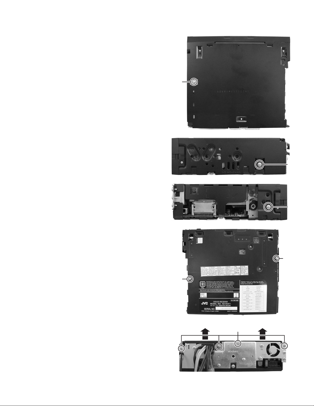
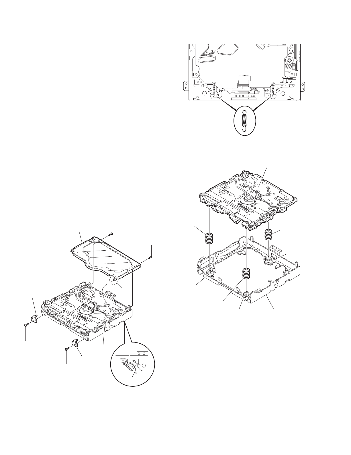
3.1 Main body
3.1.1 Removing the Side heat sink
(Fig.1)
(1) From the left side of the main body, remove the two screws
A and Two screws B attaching the Side heat sink.
A
B
Fig.1
1-10 (No.MA304)
Page 12
3.1.2 Removing the Top chassis assembly
(See Fig.2 to 6)
(1) From the top side of the main body, remove the one screw
C attaching the Top chassis assembly. (See Fig.2)
(2) From the both sides of the main body, remove the two
screws D attaching the Top chassis assembly. (See Fig.3
and 4)
(3) From the bottom side of the main body, remove the two
screws E attaching the Top chassis assembly. (See Fig.5)
(4) From the back side of the main body, remove the four
screws F attaching the Top chassis assembly. (See Fig.6)
(5) Lift the Top chassis assembly in the direction of the arrow.
(See Fig.6)
C
Fig.2
D
E
Fig.3
D
Fig.4
E
Fig.5
Fig.6
F
(No.MA304)1-11
Page 13
3.1.3 Removing the Front chassis assembly
(See Fig.7 and 8)
(1) From the both sides of the Top chassis assembly, remove
the two screws G attaching the Front chassis assembly.
(See Fig.7 and 8)
3.1.4 Removing the DVD mechanism assembly
(See Fig.9)
(1) From the inside of the Top chassis assembly, remove the
three screws H attaching the DVD mechanism assembly
and take out the DVD mechanism assembly.
(2) From the side of the DVD mechanism assembly, remove
the double-stick tape fixing the insulator.
(3) Remove the insulator from the DVD mechanism assembly.
G
Fig.7
G
Fig.8
HH
1-12 (No.MA304)
H
Fig.9
Page 14
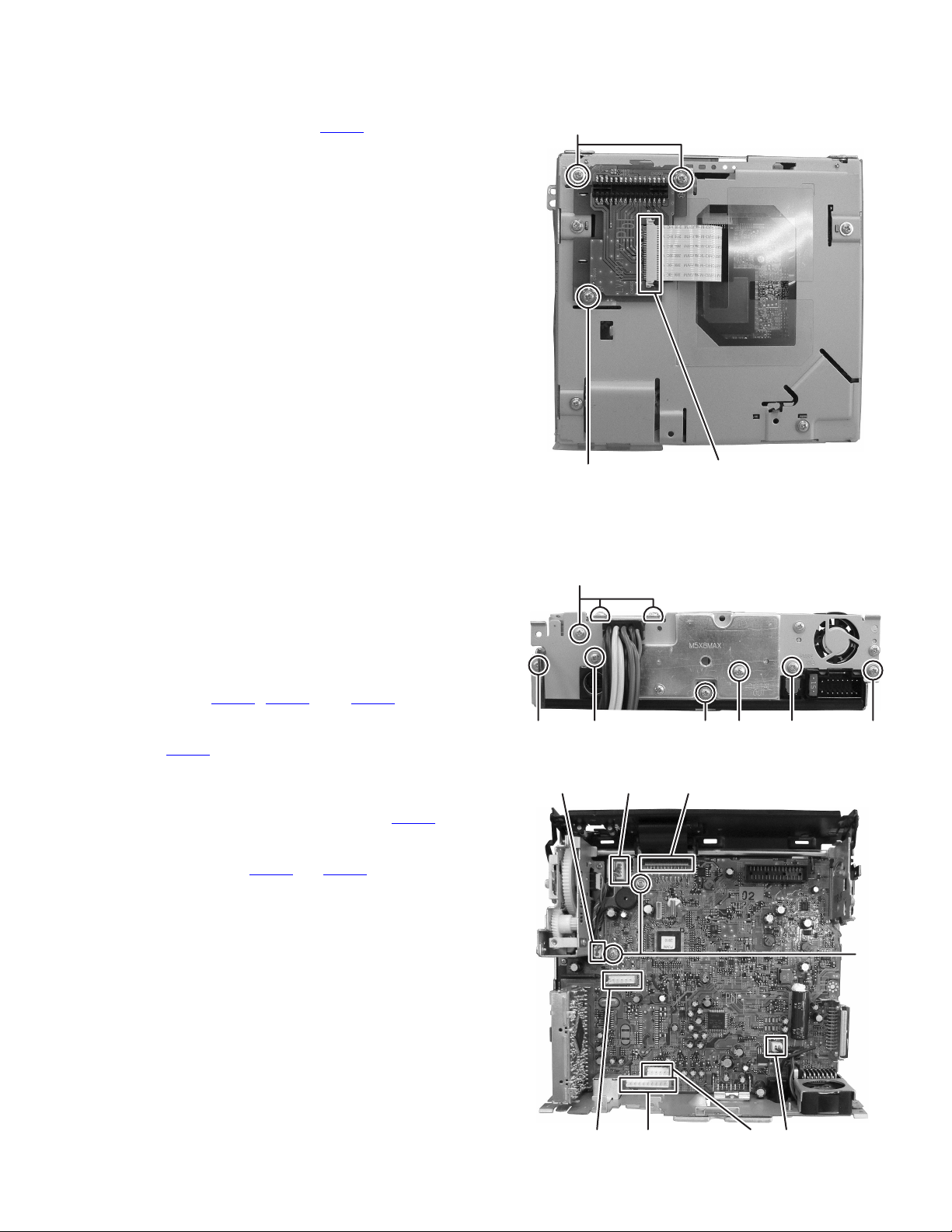
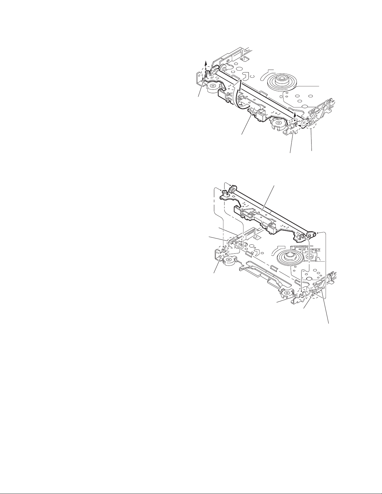
3.1.5 Removing the Connection board assembly
(See Fig.10)
(1) From the bottom side of the DVD mechanism assembly, re-
lease the lock of the connector CN965
board assembly and disconnect the card wire.
(2) Remove the three screws J attaching the Connection
board assembly on the DVD mechanism assembly. And remove the connection board assembly.
on the Connection
J
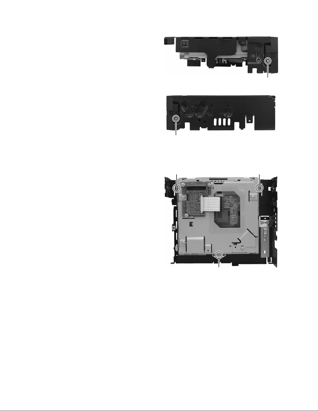
3.1.6 Removing the Rear bracket
(See Fig.11 and 12)
(1) Remove the one screw K attaching the Antenna cable, re-
move the one screw L attaching the CD-CH jack, remove
the one screw M attaching the IC bracket, remove the one
screw N attaching the Digital out jack and remove the two
screws P attaching the Rear bracket. (See Fig.11)
(2) Remove the three screws Q attaching the Wire holder.
(See Fig.11)
(3) Disconnect the connector wires from car cables connected
to connector CN931
board assembly. (See Fig.12)
(4) Disconnect the connector wire from Fan connected to con-
nector CN861
3.1.7 Removing the Main board assembly
(See Fig.12)
(1) Disconnect the card wire from connector CN962
Main board assembly.
(2) Disconnect the connector wire from Gear assembly con-
nected to connector CN881
assembly.
(3) Remove the two screws R attaching the Main board as-
sembly.
, CN311, and CN361 on the Main
on the Main board assembly. (See Fig.12)
on the
and CN891 on the Main board
J
CN965
Fig.10
Q
KL MNPP
Fig.11
CN962CN891CN881
CN931 CN361 CN311 CN861
Fig.12
(No.MA304)1-13
R
Page 15
3.1.8 Removing the Front door mechanism assembly
(See Fig.13)
(1) From the top side of the bottom chassis assembly, remove
the three screws S attaching the FPC guide to the Bottom
chassis assembly.
(2) Remove the five screws T attaching the Front door mech-
anism assembly to the Bottom chassis.
REFERENCE:
When attaching the screws S and T, apply a locking agent
them.
3.1.9 Removing the panel A control board assembly and panel B control board assembly
(See Fig.14 and 15)
(1) Remove the eight screws U attaching the Rear cover. (See
Fig.14)
(2) Remove the two screws V attaching the panel B control
board. (See Fig.15)
STT
U
Fig.13
U
Fig.14
V
Fig.15
1-14 (No.MA304)
Page 16
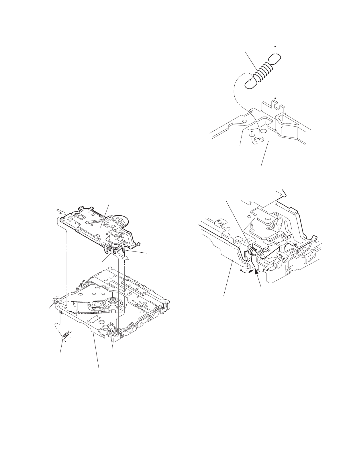
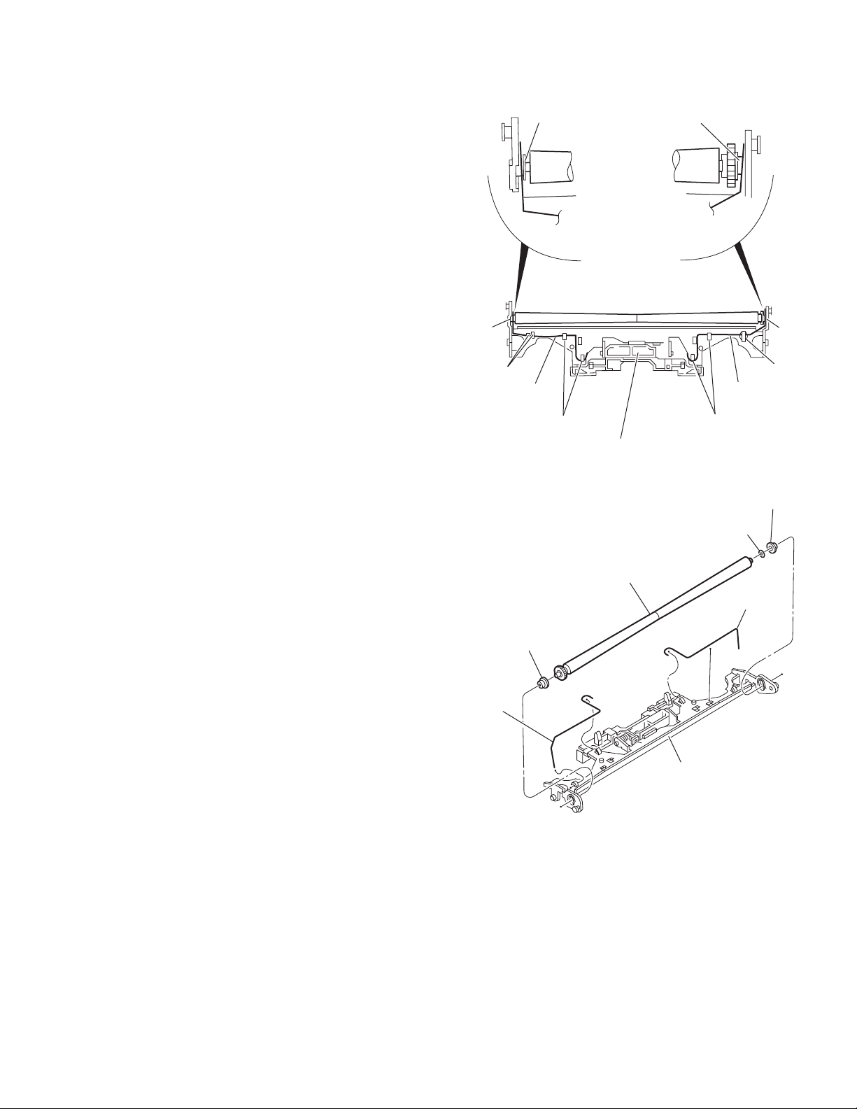
3.2 DVD mechanism assembly
3.2.1 Removing the mechanism control board
(See Fig.1)
Caution:
Before disconnecting the flexible wire extending from the DVD
pickup, solder the short-circuit point on the flexible wire using
a grounding soldering iron. If you do not follow this instruction,
the DVD pickup may be damaged.
(1) Turn over the body, and solder the short-circuit points on
the flexible wire extending from the DVD pickup.
(2) Disconnect the flexible wire from connector CN101
mechanism control board.
(3) Disconnect the card wire from connector CN201
mechanism control board.
(4) Disconnect the flexible wire from connector CN202
mechanism control board.
(5) Unsolder two soldered points a on the mechanism control
board and remove the wire extending from the feed motor.
(6) Remove the screw A attaching the lug wire.
(7) Remove the two screws B and screw C attaching the
mechanism control board.
Caution:
• As the flexible wire to be connected to CN101
attach it to the mechanism control board using a double
tape.
• After reassembling, unsolder the short-circuit points.
on the
on the
on the
, make sure to
Flexible wire
Double tape
CN101
B
Short-circuit points
A
Lug wire
B
CN201
Feed motor
a
C
CN202
Mechanism control board
Fig.1
(No.MA304)1-15
Page 17
3.2.2 Removing the top cover
(See Fig.2)
(1) Remove the two screws D attaching the top cover on the
back of the body.
(2) Remove the top cover upward.
Reference:
When reassembling, set part b of the top cover under the
bending part c of the chassis frame.
3.2.3 Removing the mechanism section
(See Fig.2 to 4)
• Remove the top cover.
(1) From the bottom of the body, remove the screw E attaching
the lug wire. (See Fig.2.)
(2) Remove the two screws F attaching the right and left stop-
pers on the front side. (See Fig.2.)
(3) Remove the two floating springs on the bottom of the body.
(See Fig.3.)
(4) Move the mechanism section upward and remove from the
chassis frame.
The three damper springs come off from the dampers.
(See Fig.4.)
Caution:
• When reassembling, reattach the damper spring to the
damper respectively and insert the three shafts on the bottom of the mechanism to the dampers.
• Before inserting the shaft to the dampers, apply IPA to the
hole of damper.
Floating spring
Fig.3
Mechanism section
Stopper
F
Top cover
Stopper
F
D
D
b
c
E
Lug wire
Damper SP.(F)
(Silver)
Damper (F)
(Black)
Damper SP.(F)
(Silver)
Damper (F)
(Black)
Fig.4
Damper SP.(R)
(Red)
Damper (R)
(Purple)
Chassis frame
1-16 (No.MA304)
Fig.2
Page 18
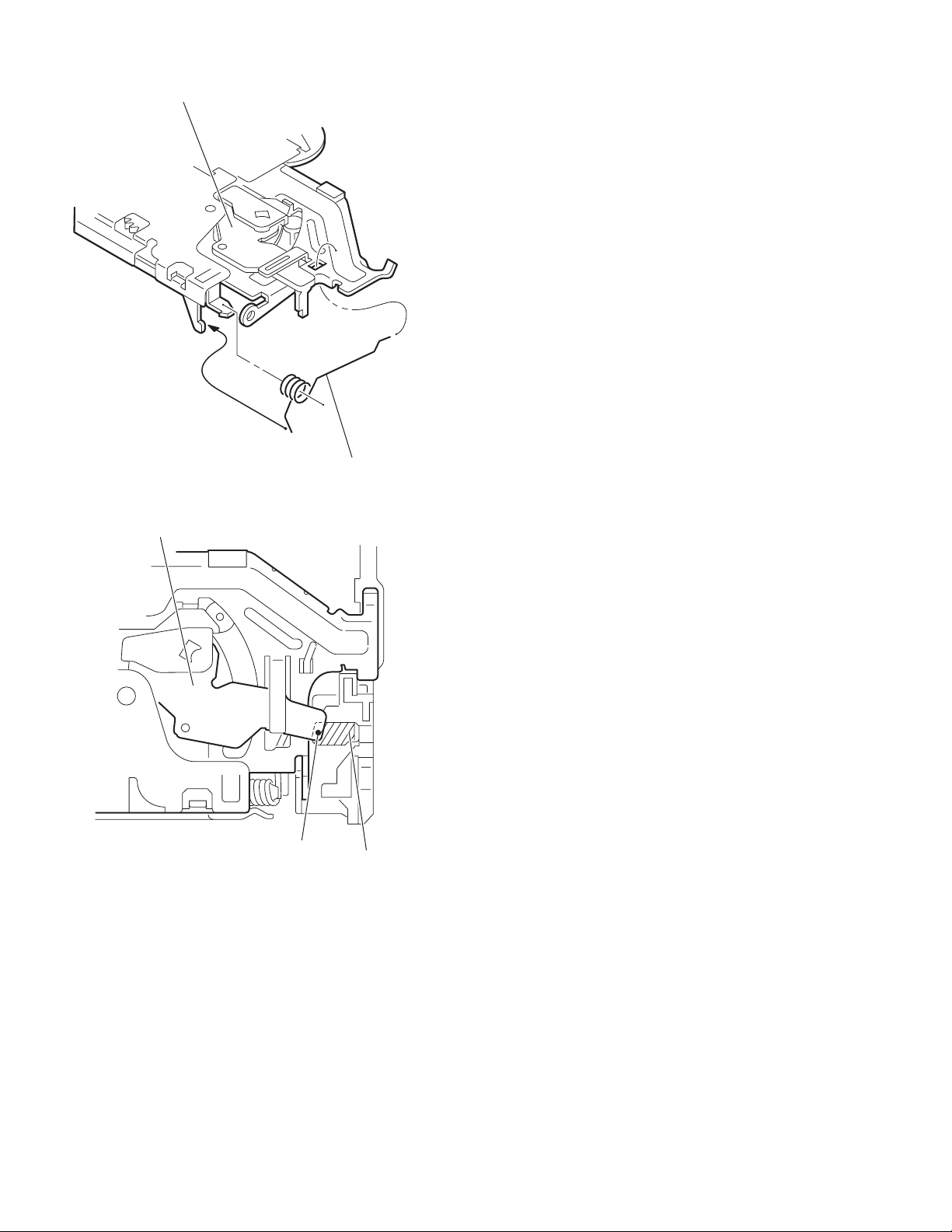
3.2.4 Removing the clamper unit
(See Fig.5 to 7)
• Remove the top cover and the mechanism section.
(1) Remove the clamper2 spring on the bottom of the mecha-
nism section. (See Figs.5.and 6.)
(2) Release the part d of the clamper spring from the bending
part of the chassis base assembly. (See Fig.7.)
(3) Move the clamper unit in the direction of the arrow and turn.
Release the two joints e and f, then remove the clamper
unit upward. (See Fig.6.)
3.2.5 Reattaching the clamper unit
(See Fig.5 to 9)
(1) Attach the clamper spring to the clamper unit. (See Fig.8.)
(2) Move the clamper unit to set the side joints e and f to each
boss of the chassis base assembly. Make sure that part g
is inserted to the notch of the chassis base assembly. (See
Figs.5 and 9.)
(3) Move the part d of the clamper spring to the outside of the
bending part of the chassis base assembly. (See Fig.7.)
(4) Attach the clamper2 spring to the chassis base assembly.
(See Figs.5 and 6.)
Caution:
When reattaching, temporarily hook the end of the clamper
spring as shown in the figure to make the work easy. (See
Fig.8.)
Clamper unit
Clamper2 spring
Chassis base assembly
Fig.6
Clamper spring
Clamper spring
f
Clamper2 spring
Chassis base assembly
g
d
Chassis base assembly
Fig.7
e
Fig.5
(No.MA304)1-17
Page 19
Clamper unit
Clamper unit
Clamper spring
Fig.8
1-18 (No.MA304)
Fig.9
g
Notch
Page 20
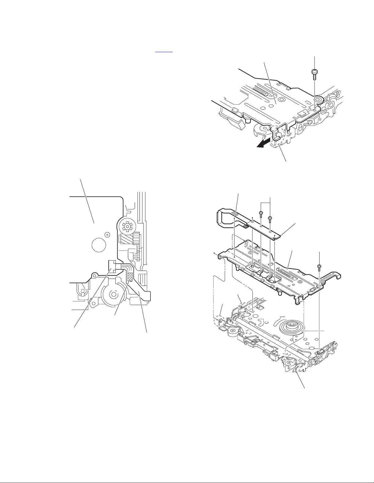
3.2.6 Removing the front unit
(See Fig.10 to 12)
• Remove the top cover and the mechanism section.
(1) Disconnect the flexible wire from connector CN202
mechanism control board at the bottom of the body. (See
Fig.10.)
(2) Remove the screw G attaching the front unit on the top of
the body. (See Fig.11.)
(3) Move the front unit toward the front to release joint h, and
release two joints i and j on the right side of the chassis
base assembly. Then remove the front unit upward. (See
Figs.11 and 12.)
(4) Remove the two screws H attaching the switch board. (See
Fig.12.)
Reference:
You can remove the switch board only without removing the
front unit.
Caution:
When reassembling, attach the flexible wire extending from
the switch board using the double tape. (See Figs.10 and 12.)
Mechanism control board
on the
G
Front unit
h
Fig.11
CN202
Double tape
Fig.10
Flexible wire
Double tape
j
i
H
Switch board
Front unit
G
Fig.12
h
(No.MA304)1-19
Page 21
3.2.7 Removing the loading arm assembly
(See Fig.13 , 14)
• Remove the top cover, the mechanism section and the front
unit.
(1) From the top of the body, move the loading arm assembly
from the front side upward, and release the bosses from
the right and left joints k and m of the chassis base assembly.
(2) Release the boss from notch n of the connect arm on the
right side of the body, and release the boss from notch p of
the slide cam assembly on the left side.
m
Loading arm assembly
Side cam
assembly
p
m
k
Fig.13
Loading arm assembly
k
n
n
Connect arm
1-20 (No.MA304)
Fig.14
Page 22
3.2.8 Removing the rod (L)(R)/roller assembly
(See Fig.15 and 16)
• Remove the top cover, the mechanism section, the front unit
and the loading arm assembly.
(1) Release the rod (L) and (R) from the joints q at the bottom
of the loading arm assembly (See Fig.15.)
(2) Remove the roller assembly from the loading arm assem-
bly. (See Fig.16.)
(3) Remove the two collars and washer from the roller assem-
bly. (See Fig.16.)
Caution:
After attaching the loading arm assembly to the roller assembly, attach the rod (L) and (R). Attach the rods to the right and
left collars of the roller. (See Fig.15.)
When reattaching the rod (L) and (R) to the loading arm assembly, engage each joint as shown in Fig.15. As joints q of
the rod (L), let the rod through q before reattaching it.
Collar
Collar
Rod(R) Rod(L)
q
q
q
Collar
Rod(L)
Rod(R)
q
Loading arm assembly
Fig.15
Roller assembly
Loading arm assembly
q
Rod(L)
q
Collar
Washer
Rod(R)
Fig.16
(No.MA304)1-21
Page 23
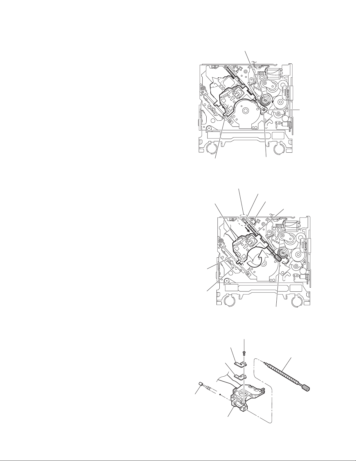
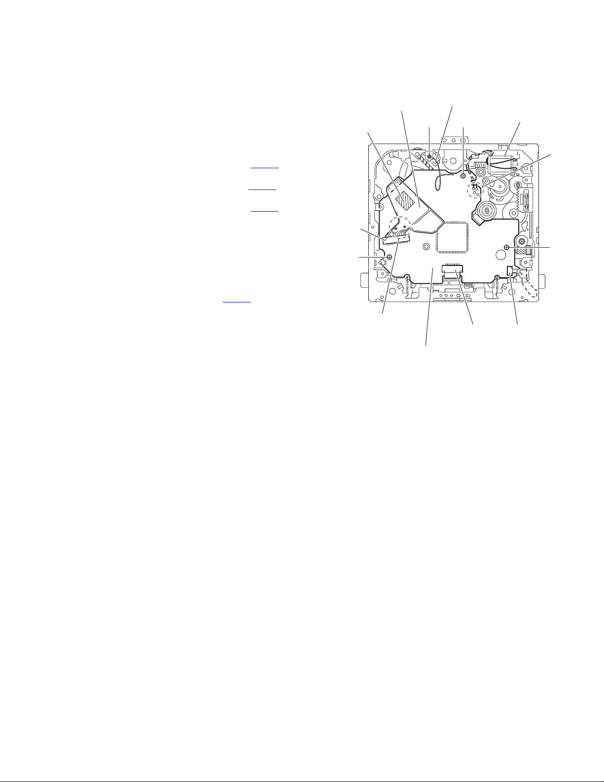
3.2.9 Removing the DVD pickup assembly
(See Fig.17 to 19)
• Remove the mechanism control board.
(1) From the bottom of the body, turn the feed gear in the di-
rection of the arrow to move the DVD pickup outwards.
(See Fig.17.)
(2) Remove the screw J attaching the thrust spring. (See
Fig.17.)
(3) Remove the DVD pickup assembly upward on the L.S.gear
side and release from sub shaft at joint r. Move the lead
screw of the DVD pickup assembly in the direction of the
arrow to release from joint s. (See Fig.18.)
Caution:
• When releasing the lead screw at joint s, the L.S.collar
comes off at the end of the lead screw. When reassembling, reattach the L.S.collar to the lead screw and
engage joint s. (See Fig.18.)
• When reattaching the L.S.collar, reattach it to the point
s of the lead screw, and to the rod (M). Make sure that
the L.S.collar is set on the rod (M) spring. (See Fig.18.)
(4) Remove the screw K attaching the rack spring/ rack plate
on the DVD pickup. (See Fig.19.)
(5) Pull out the lead screw. (See Fig.19.)
Caution:
Perform adjustment after replacing the pickup.
DVD Pickup assembly
DVD Pickup assembly
Feed gear
J
Thrust spring
Fig.17
s
L.S.collar
Rod(M)
Lead screw
Sub shaft
L.S.collar
r
L.S.gear
Fig.18
K
Rack spring
Lead screw
Rack plate
DVD Pickup
Fig.19
1-22 (No.MA304)
Page 24

3.2.10 Removing the spindle motor
r
(See Fig.20)
• Remove the mechanism control board.
Remove the two screws L attaching the spindle motor on the
bottom of the body.
Caution:
Perform adjustment when reattaching the spindle motor.
3.2.11 Removing the feed motor assembly
(See Fig.21 and 22)
• Remove the mechanism control board.
(1) Remove the feed TRI. spring on the bottom of the body.
(See Fig.21.)
(2) Remove the two screws M attaching the feed motor as-
sembly. (See Fig.21.)
(3) Remove the slit washer from the motor H. assembly and
pull out the worm wheel. (See Fig.22.)
Remove the two screws N attaching the feed motor. (See
Fig.22.)
Spindle motor
Feed TRI. spring
L
Fig.20
M
Feed motor assembly
Fig.21
Slit washer
Worm wheel
Feed moto
N
Motor H. assembly
Fig.22
(No.MA304)1-23
Page 25

SECTION 4
ADJUSTMENT
4.1 Test instruments required for adjustment
(1) Digital oscilloscope (100MHz)
(2) Jitter meter
(3) Digital tester
(4) Electric voltmeter
(5) Tracking offset meter
(6) Test Disc : VT501 or VT502
(7) Extension studs : STDV001-3P
(8) Extension cable : EXTDV002-30P
4.3 Connection method
Connection procedure
(1) Attach the front chassis assembly to the main board.
(2) Attach the heat sink and rear bracket to the main board.
(3) Attach the extension studs to the DVD mechanism assembly.
(4) Connect the DVD mechanism assembly and the main board with a extension cable.
4.2 Standard measuring conditions
Power supply voltage : DC14.4V(11 to 16V)
Load impedance : 4 Ω (2 Speakers connection)
Line Output : 20K Ω
Caution:
Be sure to attach the heat sink and rear bracket onto the power
amplifier IC and regulator IC respectively, before supply the
power. If voltage is applied without attaching these parts, the
power amplifier IC and regulator IC will be destroyed by heat.
Extension cable
EXTDV002-30P
Extension studs
STDV001-3P
Extension stud
STDV001-3P
1-24 (No.MA304)
Page 26

4.4 Adjustment method for jitter
After replacing the pickup, set the unit in the service mode to display a jitter value on the LCD.
Confirm that the jitter value measured with a jitter meter is within 12% of the jitter value displayed on the LCD.
If it is within 12%, then adjustment is not necessary.
If the measured jitter value is outside the 12% tolerance range, perform the following adjustments.
4.4.1 Adjustment procedure
(1) Set the unit to the service mode and display a jitter value (hex data) on the LCD.
(2) Turn each of the screws a, b and c, by a half-turn per step, in the direction that reduces the jitter value in order to minimize it.
(Do not turn a screw more than a half turn at a time, but adjust the screws in the cycle of the same level is turned in the pair of
b+c and the same level is turned in the pair of a+b.)
(3) After completing the adjustment, secure the screws with screw lock paint.
c
b
a
Jitter value adjustment procedure (Pickup horizontal level adjustment relative to the DVD recording surface)
(For the adjustment tool use a 3 mm wrench and not a screwdriver, this procedure will make the adjustment easier.)
3 mm wrench
(1) Set the unit to the service mode and display a jitter value (hex data) on the LCD.
(2) Turn each of the screws a, b and c, by a half-turn per step, in the direction that reduces the jitter value in order to minimize it.
(Do not turn a screw more than a half turn at a time, but adjust the screw in the cycle of same level turn by pair of b+c → pair of
a+b.)
(3) After completing the adjustment, secure the screws with screw lock paint.
(No.MA304)1-25
Page 27

4.5 Jitter value conversion table
Load the test DVD and set the unit to the service mode. A jitter value converted to the hex value is displayed on the LCD.
Refer to the corresponding decimal notation value shown in the following Jitter Conversion Table.
The adjustment is OK if the jitter value measured with a jitter meter is within 12% of the jitter value displayed on the LCD.
If the measured jitter value is outside the 12% tolerance range, adjust it to minimize the difference between the measured value and
the displayed value.
Jitter conversion value (DV2.1)
SPEED 1
Calculation
Indicated on the LCD Jitter (%)
E9A6
7.5
LCD
indication
Jitter value
(%)
LCD
indication
Jitter value
(%)
LCD
indication
Jitter value
(%)
LCD
indication
Jitter value
EF56 4.7 E972 7.6 E38E 10.5 DDAA 13.4
EF22 4.8 E93E 7.7 E35A 10.6 DD76 13.5
EEEE 4.9 E90A 7.8 E326 10.7 DD42 13.6
EEBA 5.0 E8D6 7.9 E2F2 10.8 DD0E 13.7
EE86 5.1 E8A2 8.0 E2BE 10.9 DCDA 13.8
EE52 5.2 E86E 8.1 E28A 11.0 DCA6 13.9
EE1E 5.3 E83A 8.2 E256 11.1 DC72 14.0
EDEA 5.4 E806 8.3 E222 11.2 DC3E 14.1
EDB6 5.5 E7D2 8.4 E1EE 11.3 DC0A 14.2
ED82 5.6 E79E 8.5 E1BA 11.4 DBD6 14.3
ED4E 5.7 E76A 8.6 E186 11.5 DBA2 14.4
ED1A 5.8 E736 8.7 E152 11.6 DB6E 14.5
ECE6 5.9 E702 8.8 E11E 11.7 DB3A 14.6
ECB2 6.0 E6CE 8.9 E0EA 11.8 DB06 14.7
EC7E 6.1 E69A 9.0 E0B6 11.9 DAD2 14.8
EC4A 6.2 E666 9.1 E082 12.0 DA9E 14.9
EC16 6.3 E632 9.2 E04E 12.1 DA6A 15.0
EBE2 6.4 E5FE 9.3 E01A 12.2 DA36 15.1
EBAE 6.5 E5CA 9.4 DFE6 12.3 DA02 15.2
EB7A 6.6 E596 9.5 DFB2 12.4 D9CE 15.3
EB46 6.7 E562 9.6 DF7E 12.5 D99A 15.4
EB12 6.8 E52E 9.7 DF4A 12.6 D966 15.5
EADE 6.9 E4FA 9.8 DF16 12.7 D932 15.6
EAAA 7.0 E4C6 9.9 DEE2 12.8 D8FE 15.7
EA76 7.1 E492 10.0 DEAE 12.9 D8CA 15.8
EA42 7.2 E45E 10.1 DE7A 13.0 D896 15.9
EA0E 7.3 E42A 10.2 DE46 13.1 D862 16.0
E9DA 7.4 E3F6 10.3 DE12 13.2
E9A6 7.5 E3C2 10.4 DDDE 13.3
(%)
1-26 (No.MA304)
Page 28

4.6 Service mode
4.6.1 Standard input/output conditions
Power supply voltage : DC14.4V(11 to 16V)
Load impedance : 4 Ω (2 Speakers connection)
Line Output : 20K Ω
4.6.2 Service mode setting procedure
(The DVD does not need to be loaded before starting the following procedure.)
4.6.3 Operation procedures
1.Service mode 1 (Indication of a service mode 1 is nothing.)
Keep this state more 2 seconds
while continuing pressing the
[STANDBY/ON ATTENUATOR] button
and [EJECT] button sequentially.
Screen indication
NO EJECT? 1
EMERGENCY EJECT? 2
Exchanging it operate a menu of a service mode with the [UP] button
and [DOWN] button. Operate choice of a menu with a [ENT] button.
1 : When an [ENT] button is pushed in NO EJECT indication, it is set
by an EJECT prohibition mode.
When an [ENT] button is pushed in EJECT OK indication, it is aet
bu a normal mode.
2 : Forced EJECT movement
A screen becomes normal indication after an ENT button was pushed.
2.Service mode 2
Keep this state more 2 seconds
while continuing pressing the
[MENU] button, [VOLUME-] button
and [ENT] button sequentially.
Screen indication
SERVICE MODE 2
INITIALIZE ALL
INITIALIZE
INITIALIZE DVD
INITIALIZE BT
Exchanging it operate a menu of a service mode with the [UP] button
and [DOWN] button. Operate choice of a menu with a [ENT] button.
A
(No.MA304)1-27
Page 29

A
INITIALIZE ALL
INITIALIZE ALL (Each EEPROM is initialized
NOW ...
INITIALIZE ALL
INITIALIZE ALL
OK
by a factory shipment state.)
EMain micon EEPROM initialization (user
entry domain, error history,
speaker setting, subarea of J-version, data
to pre-set )
EPanel micon EEPROM initialization
(picture adjustment data)
EDVD unit EEPROM initialization (except
a permanent domain)
EBluetooth (Module/Hideaway) EEPROM
initialization
EAfter clear completion, a screen returns
to normal indication after OK indication
INITIALIZE
was displayed for three seconds.
INITIALIZE (Initialization of a user area of
NOW ...
INITIALIZE
INITIALIZE
OK
each EEPROM)
EMain micon EEPROM initialization
(a user entry domain )
(a user entry domain, speaker setting,
subarea of J-version, data to pre-set )
EPanel micon EEPROM initialization
(picture adjustment data )
EDVD unit EEPROM initialization (except
a permanent domain)
EAfter clear completion, a screen returns
to normal indication after OK indication
was displayed for three seconds.
INITIALIZE DVD
Full initialization of EEPROM of a DVD unit
INITIALIZE DVD
OK
( It is included a permanent domain)
After clear completion, this indication is continued
till an effective key is input.
3.Service mode 3
Keep this state more 2 seconds
while continuing pressing the
[MENU] button, [DISP] button
and [ENT] button sequentially.
Screen indication
SERVICE MODE 3
SERVICE MODE
INITIALIZE ALL
RUNNING MODE
Exchanging it operate a menu of a service mode with the [UP] button
and [DOWN] button. Operate choice of a menu with a [ENT] button.
A
INITIALIZE BT
INITIALIZE BT
OK
Full initialization of EEPROM of Bluetooth ( Module/Hideaway )
After clear completion, this indication is continued
till an effective key is input.
1-28 (No.MA304)
Page 30

A
SERVICE MODE
SERVICE MODE
VERSION
AREA/REGION
TEMPERATURE
SERVICE MODE
ERROR READ
ERROR CLEAR
BT VERSION
MEMORY CHECK
DVD NTSC/PAL
DVD CHECK MODE
Exchanging it operate a menu
of a service mode with the [UP]
button and [DOWN] button.
Operate choice of a menu with
a [ENT] button.
Return to previous menu with
a [BACK] button.
VERSION
MAIN
JD8
CH
PANEL
P.DADJ
V [ ]
V V [ ]
Micon version indication
Main micon version and
ROM correction version
JD8 version
CH version
Panel micon version and
ROM correction version
00 : Panel No adjustment
(factory use)
01 : Complete Panel
adjustmen (factory use)
AREA/REGION
SYS-AREA :
JD8-AREA :
JD8-REGION :
JD8-CPPM : N FFFF
Area and region indicattion
Main micon area
JD8 area
JD8 region
CPPM does not have
KD-AVX11
TEMPERATURE Temperature data reading
ETemperature data by the temperature sensor in
the main micon and JD8-PCB is read every 5
seconds and displayed in hex numbers.
MEMORY CHECK ( It is displayed only at the time of
the disc insertion )
Memory residual quantity indication mode
Data residual quantity of a disc is displayed by LCD.
About the playback control-related key ([FSKIP],
[BSKIP],[UP], [DOWN], [VOL]), only movement is
effective.
Indication does not change as memory residual
quantity indication.
About cancellation of this mode, press the
[STANDBY/ON ATTENUATOR] button.
DVD NTSC/PAL
NTSC
PAL
DVD picture change
JD8 output picture setting
(NTSC)
JD8 output picture setting
(PAL)
DVD CHECK MODE
See "DVD CHECK MODE" for details.
ERROR READ
DVD ERROR READ
CH ERROR READ
MECHA ERROR READ
READ ALL
A B C
(No.MA304)1-29
Page 31

A B
C
DVD ERROR READ
Reading of a DVD unit error history
CH ERROR READ
Reading of a CD changer error
history
MECHA ERROR READ
Reading of a door mechanism error
history
READ ALL
Reading of a main micon EEPROM
(All contents)
INITIALIZE ALL
NOW ...
INITIALIZE ALL
RUNNING MODE
See "Running mode" for details.
ERROR CLEAR
DVD ERROR CLEAR
CH ERROR CLEAR
MECHA ERROR CLEAR
BT VERSION
SW BT CORE
HW BT MODULE
SW BT MODULE
SW HIDEAWAY
ADR-
INITIALIZE ALL
OK
Clear of each error history
A screen returns to
following indication after
clear completion.
Bluetooth version
indication
(When connect Blue tooth adapter, it is
displayed)
Software version of
BT core
Hardware version of
BT Module
Software version of
BT Module
Software version of
BT Hideaway controller
BT Address
INITIALIZE ALL (Each
EEPROM is initialized by
a factory shipment state.)
Main micon EEPROM
initialization (user entry
domain, error history,
speaker setting, subarea
of J-version, data to pre set )
Panel micon EEPROM
initialization (picture
adjustment data)
DVD unit EEPROM
initialization (except a
permanent domain)
Bluetooth
(Module/Hideaway)
EEPROM initialization
After clear completion,
a screen returns to
normal indication after
OK indication was
displayed for three
seconds.
1-30 (No.MA304)
Page 32

4.Service mode 4
Keep this state more 2 seconds
while continuing pressing the
[BACK] button, [MENU] button
and [DISP] button sequentially.
Screen indication
SERVICE MODE 4
RDS S MODE
MONITOR S MODE
Exchanging it operate s menu of a service mode with the [UP] button
and [DOWN] button. Operate choice of a menu with a [ENT] button.
RDS S MODE
RDS service mode (Only RDS model)
MONITOR S MODE
R/W CHROMA 1
R/W CHROMA 2
DATA CLEAR
4.6.4 DVD check mode
DVD CHECK MODE
NORMAL PLAY
EF OUT-TRACKING OFF
EF IN-TRACKING OFF
CD-LASER ON
DVD-LASER ON
DVDx1 JITTER MODE
DVD CHECK MODE
EEPROM DATA DISP
EEPROM DATA CLEAR
TEMPERATURE
SEARCH & JITTER
MONITOR
PLAY
Exchanging it operate a menu of a service mode with the [UP] button
and [DOWN] button. Operate choice of a menu with a [ENT] button.
Command
NORMAL PLAY
EF OUT-TRACKING OFF
EF IN-TRACKING OFF
CD-LASER ON
DVD-LASER ON
DVDx1 JITTER MODE
EEPROM DATA DISP
EEPROM DATA CLEAR
TEMPERATURE
SEARCH & JITTER
MONITOR
PLAY
STOP
OPEN
Mechanism unit operation
Start at normal speed
(After start, jitter is measured by an inner position.)
Tracking off the outermost position of CD
Tracking off the innermost position of CD
CD_LD lights and laser current is displayed.
DVD_LD lights and laser currrent is displayed
DVD x1 jitter measuring mode
(for use in mechanism adjustment)
Contents of EEPROM is displayed.
Contents of EEPROM is initialized.
Temperature indication
The search and jitter measurement to an appointed
position of DVD.
Monitor terminal setting
DVD x1 stopped start
(After start, jitter is measured by an inner position.)
Disc stopped, LD-OFF
OPEN
See "Monitor adjustment" for details.
CHROMA DATA read/write of NTSC/PAL signal processing IC
CHROMA DATA read/write of TFT driver IC
Clear of CHROMA DATA of 1,2 (return to an initial value)
DVD CHECK MODE
STOP
OPEN
Indication contents
Laser current value, jitter value
For EF phase error
For EF phase error
Laser current value, jitter value
Laser current value, jitter value
Laser current value, jitter value
EEPROM address
EEPROM contents
EEPROM address
EEPROM contents
Temperature is displayed in hex
numbers.
Position measured with VT-501
jitter value
Not displayed.
Not displayed.
Not displayed.
(No.MA304)1-31
Page 33

4.6.5 Error code tables
Mechanism error code
Error contents
Disc loading error
B1 time out
C1 time out
D1 time out
C2 time out
B2 time out
A2 time out
F1 time out
A0 (Switch state without existence)
G1 time out
G2 time out
Eject error
F2 time out
A1 time out
B1 time out
C1 time out
D1 time out
C2 time out
B2 time out
A0 (Switch state without existence)
Error in loading wait
Loading re-execution ¨ NG ¨ Eject
Eject re-execution ¨ NG ¨ Loading
Details
Loading of a running mode
Disc was pulled out in a wait.
Running mode error
Running mode error
Error code
0x09
0x09
0x09
0x09
0x09
0x09
0x09
0x09
0x09
0x09
0x01
0x01
0x01
0x01
0x01
0x01
0x01
0x01
0x09
0x09
0x01
Detailed error code
0x0011
0x0012
0x0013
0x0014
0x0015
0x0016
0x0017
0x0018
0x0019
0x0020
0x0021
0x0022
0x0023
0x0024
0x0025
0x0026
0x0027
0x0028
0x0031
0x0032
0x0033
Disc error code
Error contents
TOC read error
First track access error
Last track access error
T1 access error
T12 access error
T24 access error
Read-in area read error
DVD L1 layer adjustment error
NO DISC judgment
It is NO DISC by start failure
It is stopped by playback inability.
Logic format NG
Details
TOC lead movement of a CD is not completed.
Even if TOC reading passes after the end with
CD running mode for 30 seconds, the first track
access is not finished.
Even if first track passes after the end with
CD running mode for 30 seconds, the last track
access is not finished.
Even if T1 access passes in a DVD runnung
mode for 30 seconds, it is not finished.
Even if T12 access passes in a DVD runnung
mode for 30 seconds, it is not finished.
Even if T24 access passes in a DVD runnung
mode for 30 seconds, it is not finished.
Read-in area read operation of DVD is not
completed.
Adjustment of L1 layer of DVD is not finishhed
normally. (including focus jump failure)
Judgment without disc
Start is impossible
Stop in running mode playback
Logic format analysis inability or
non-correspondence logic format
Error code
0x84
0x80
0x80
0x80
0x80
0x80
0x84
0x80
0x80
0x80
0x80
0x80
Detailed error code
0x0059
0x0060
0x0061
0x0069
0x0070
0x0071
0x0072
0x0074
0x0090
0x0091
0x0093
0x0094
1-32 (No.MA304)
Page 34

Error codes of panel mechanism
PANEL ANGLE
Open error
1. Time out error by OPEN position cannot detect.
Close error (ANGLE 1 error)
1. Time out error by ANGLE 1 position cannot detect.
Angle positioning error
Moving to 10 degrees (ANGLE 2 error)
1. Time out error by ANGLE 2 position cannot detect at moving to open position.
2. Missing to ANGLE 1 and detected ANGLE 2 position at moving to open position.
3. Time out error by ANGLE 2 cannot detect at moving close position.
Moving to 20 degrees (ANGLE 3 error)
1. Time out error by ANGLE 3 position cannot detect at moving to open position.
2. Missing to ANGLE 2 and detected ANGLE 3 position at moving to open position.
3. Time out error by ANGLE 3 cannot detect at moving close position.
Moving to 30 degrees (ANGLE 4 error)
1. Time out error by ANGLE 4 position cannot detect at moving to open position.
2. Missing to ANGLE 3 and detected ANGLE 4 position at moving to open position.
3. Time out error by ANGLE 4 cannot detect at moving close position.
Abnormal switch position at moving panel
The Panel move to open and close position, detected abnormal switch position.
4.6.6 Running mode
2
3
4
Open
Panel1
Detail
Close
10 degrees
20 degrees
30 degrees
Open
Main Body
Error code
(Service mode)
0A0001
0B0006
0D0021
0D0022
0D0023
0E0031
0E0032
0E0033
0F0041
0F0042
0F0043
0A0000
Indication
RUNNING1 MECHA
RUNNING2 MECHA
Explanation
Door mecha running 1
Door mecha running 2
Operation contents of 1 cycle
Panel close ¨ Panel open
Panel close ¨ Panel open
¨ Panel detach position ¨Panel angle
RETRY
3 position ¨ Panel angle 1 position
RUNNING3 DVD
DVD+Door mecha running1
¨ Panel angle 2 position
Loading ¨ Eject ¨ Wait for 5 seconds+
NO RETRY
Door open/close
RUNNING4 DVD
DVD+Door mecha running2
Loading ¨ Eject ¨ Wait for 5 seconds+
Door open/close
RUNNING5 DVD
DVD+Door mecha running3
Loading ¨ Playback ¨ Eject ¨ Wait for
5 seconds+Door open/close
RUNNING6 DVD
DVD+Door mecha running4
Loading ¨ Playback ¨ Eject ¨ Wait for
5 seconds+Door open/close
RUNNING7 DVD
DVD+Door mecha running5
Loading ¨ Playback ¨ Eject ¨ Wait for
5 seconds+Door open/close
RUNNING8 DVD
DVD+Door mecha running6
Loading ¨ Playback ¨ Eject ¨ Wait for
5 seconds+Door open/close
Cancellation of running1,2 : Press the [EJECT] key
In running 1,2 cancellation, a door does not stop at the position and moves to a panel position.
Cancellation of running3 to 8 : Press the [POWER] key
The number of count and an error cord are displayed in running.
In
mecha error
-
Retry
Stop
Stop
Retry
Stop
Retry
Stop
Retry
In
disc error
-
-
-
-
-
Stop
Stop
Retry
Retry
(No.MA304)1-33
Page 35

Playback contents in a running mode
r
CD
The first track is played for 30 seconds. The last track is played for 30 seconds.
(The last track is played in the case of less than till the last for 30 seconds.)
DVD
2layer disc (Pit disc)
Title 1 (the L0 layer internal circumference) is played for 30 seconds. Title 12 (L0 layer circumference) is played for
30 seconds.
¨ Title 24 (L1layer internal circumference) is played for 30 seconds.
2layer disc (Recordable disc)
Title 1 (the L0 layer internal circumference) is played for 30 seconds. Title 13 (L0 layer circumference) is played fo
30 seconds.
¨ Title 24 (L1layer internal circumference) is played for 30 seconds.
1layer disc
First chapter of title 1 is played for 30 seconds. The last chapter of title 1 is played for 30 seconds.
4.6.7 Monitor adjustment
Monitor adjustment
When adjusting, switch on the main unit and insert a test disc (VT-501). And play the test disc and pause it.
(Exiti for VCO FREE-RUN adjustment)
1. Set the service mode 4.
2. Exchanging it operate a menu of a service mode with the [UP] button and [DOWN] button.
3. Change data with the [B.SKIP]/[F.SKIP] buttons.
4. Write data with a [ENT] button.
*When performing the VCO FREE-RUN(NTSC) adjustment, set the NTSC mode (Service mode 3 Service mode DVD
NTSC/PAL) and turn the input into the no input. Connect the frequency counter to the point (TP524-GND) on the panel
board and set the frequency into 15.734 0.01 (kHz).
*When performing the VCO FREE-RUN(PAL) adjustment, set the PAL mode (Service mode 3 Service mode DVD
NTSC/PAL) and turn the input into the no input. Connect the frequency counter to the point (TP524-GND) on the panel
board and set the frequency into 15.625 0.01 (kHz).
R/W CHROMA 1
Indication
Contrast
Color (NTSC)
Color (PAL)
Color (SECAM)
Tint (NTSC)
Tint (PAL)
Tint (SECAM)
Sharpness
Brightness
ABL off
Sub Contrast
White Lim
Black Lim
Gamma 1
Gamma 2
Sub Brt R
Sub Brt B
Drive R (NTSC)
Drive R (PAL)
Drive R (SECAM)
RY Gain
RY Phase (NTSC)
RY Phase (PAL)
Minimum
value
00
00
00
00
00
00
00
00
00
00
00
00
00
00
00
00
00
00
00
00
00
00
00
Maximum
value
7F
7F
7F
7F
7F
7F
7F
3F
FF
01
0F
0F
0F
FF
FF
0F
0F
3F
3F
3F
01
01
01
Reference
Initial
value
5E
33
32
3F
3C
3F
3F
20
89
01
09
0F
00
00
00
09
09
20
20
2F
00
00
00
register
value
5C
39
36
3F
3E
40
3F
20
96
01
09
0F
00
00
00
08
08
20
20
2F
00
00
00
Adjust
Adjust
Adjust
Fix
Adjust
Adjust
Fix
Fix
Adjust
Fix
Fix
Fix
Fix
Fix
Fix
Adjust
Adjust
Fix
Fix
Fix
Fix
Fix
Fix
Detail
Contrast control
Color control
Color control
Color control
Tint control
Tint control
Tint control
Sharpness control
Brightness control
Auto brightness limiter off
Controls the Y amplitude
White clipping voltage for RGB signal exceeding
over white
White clipping voltage for RGB signal exceeding
over white
Correction peak point
Boost gain correction peak point
Sub brightness control for R output signal
Sub brightness control for R output signal
Gain control for RGB video signal
Gain control for RGB video signal
Gain control for RGB video signal
Relative amplitude of R-Y color difference signal
Relative phase of G-Y color difference signal
Relative phase of G-Y color difference signal
1-34 (No.MA304)
Page 36

RY Phase (SECAM)
Drive G (NTSC)
Drive G (PAL)
Drive G (SECAM)
GY Gain
GY Phase (NTSC)
GY Phase (PAL)
GY Phase (SECAM)
Drive B (NTSC)
Drive B (PAL)
Drive B (SECAM)
Com Amp
Com DC
AFC2 Phase
DRVSEL
Unknown 1
Unknown 2
LPF
Unknown 3
DOTCLK Freq. Range
EXCHFI
PLL offset (NTSC)
PLL offset (PAL)
PLL offset (SECAM)
VD Phase (NTSC)
HD Phase (NTSC)
S GP Phase
S-ID Sense
S-ID M
HP Boost
P/N ID S
BPF/HPF
SECAM R-Y Black Adj
SECAM B-Y Black Adj
Gamma2-R
Gamma2-G
Gamma2-B
VD Phase (PAL)
VD Phase (SECAM)
HD Phase (PAL)
HD Phase (SECAM)
00
00
00
00
00
00
00
00
00
00
00
00
00
00
00
00
00
00
00
00
00
00
00
00
00
00
00
00
00
00
00
00
00
00
00
00
00
00
00
00
00
FF
FF
01
01
01
07
03
3F
3F
3F
07
1F
03
01
01
01
01
01
0F
0F
03
03
03
07
07
1F
1F
01
3F
3F
3F
01
01
01
01
3F
3F
3F
07
03
01
00 00 Fix Relative phase of G-Y color difference signal
20
20
2F
00
00
00
00
20
20
2F
80
80
04
00
00
00
01
00
07
01
28
32
2F
00
14
00
00
00
00
00
00
00
00
00
00
00
00
00
14
10
20
20
2F
00
00
00
00
20
20
2F
80
80
04
00
00
00
01
00
07
01
28
32
2F
00
14
00
00
00
00
00
00
00
00
00
00
00
00
00
14
00
Fix
Fix
Fix
Fix
Fix
Fix
Fix
Fix
Fix
Fix
Fix
Fix
Fix
Fix
Fix
Fix
Fix
Fix
Fix
Fix
Fix
Fix
Fix
Fix
Fix
Fix
Fix
Fix
Fix
Fix
Fix
Fix
Fix
Fix
Fix
Fix
Fix
Fix
Fix
Fix
Gain control for RGB video signal
Gain control for RGB video signal
Gain control for RGB video signal
Relative amplitude of R-Y color difference signal
Relative phase of G-Y color difference signal
Relative phase of G-Y color difference signal
Relative phase of G-Y color difference signal
Gain control for RGB video signal
Gain control for RGB video signal
Gain control for RGB video signal
Common pulse amplitude
Peference DC output
AFC2 phase control
Driving ability of pulse output stage
LPF
DOTCLK adjustment
VD phase phase
DOTCLK adjustment
DOTCLK adjustment
DOTCLK adjustment
VD out phase
HD out phase
SECAM gate pulse phase
SECAM ID sensitivity
SECAM ID mode
Enhance the higher side of SECAM bell filter
PAL / NTSC ID sensitivity for digital comb filter
Select chroma BPF frequency response
R-Y black level adjust for SECAM
R-Y black level adjust for SECAM
VD out phase
VD out phase
HD out phase
HD out phase
(No.MA304)1-35
Page 37

R/W CHROMA 2
Indication
USER-BRIGHT
SUB-BRIGHT R
SUB-BRIGHT B
CONTRAST
SUB-CONTRAST R
SUB-CONTRAST B
GAMMA 1
GAMMA 2
COM-LEVEL
COM-DC (NTSC)
VCO 11 (NTSC)
VCO 11 (PAL)
LPF
TRAP
SLCLP1
SLCLP0
H-POSITION (NTSC)
S/H-POSITION
HDO-POSITION
SLPAIR
BLK-POSITION
S/H-POSITION2
H POSITION (NTSC)
H-POSITION (PAL)
VCO 33 (NTSC)
VCO 33 (PAL)
COM-DC (PAL)
H POSITION (PAL)
Minimum
value
00
00
00
00
00
00
00
00
00
00
00
00
00
00
00
00
00
00
00
00
00
00
00
00
00
00
00
00
Maximum
value
FF
7F
7F
FF
7F
7F
7F
7F
7F
7F
FF
FF
07
01
01
01
3F
07
1F
01
1F
07
0F
3F
FF
FF
7F
0F
Initial
value
B1
4D
46
45
50
4B
45
00
28
3F
4B
4F
00
00
00
01
2B
01
00
00
10
00
00
2C
C5
CB
34
00
Reference
register
value
AC
4A
44
4A
5B
4C
45
00
28
3F
15.734
0.01(kHz)
15.625
0.01(kHz)
00
00
00
01
2C
01
00
00
10
00
2C
2C
B5
B5
32
00
Adjust
Adjust
Adjust
Adjust
Adjust
Adjust
Fix
Fix
Fix
Fix
Adjust
Adjust
Fix
Fix
Fix
Fix
Fix
Fix
Fix
Fix
Fix
Fix
Fix
2Fix
Fix
Fix
34
00
Detail
Brightness control
Sub brightness control for R output signal
Sub brightness control for R output signal
Contrast control
Controls the Y amplitude
Controls the Y amplitude
Correction peak point
Boost gain correction peak point
COM-LEVEL
Peference DC output
VCO FREE-RUN adjustment (NTSC)
VCO FREE-RUN adjustment (PAL)
LPF
TRAP
SLCLP1
SLCLP0
H-POSITION
S / H POSITION
HDO-POSITION
SLPAIR
BLK-POSITION
S / H POSITION2
H-POSITION
VCO FREE-RUN adjustment (NTSC)
VCO FREE-RUN adjustment (PAL)
Peference DC output
1-36 (No.MA304)
Page 38

SECTION 5
TROUBLESHOOTING
5.1 16 PIN CORD DIAGRAM (for J, U, UN, UT, A version)
BK
RD
BL
WH
BR
OR
Black
Red
Blue
White
Brown
Orange
1
BK
1
8
7
6
5
4
3
2
GN
GN/BK
VI/BK
VI
BL
BL/WH
RD
BK
WH
WH/BK
GY/BK
GY
BR
YG
OR/WH
YL
GN
VI
GY
YL
YG
10
11
12
13
14
15
16
9
Green
Violet
Gray
Yellow
YellowGreen
LOCKING THE WIRE WITH INSULOK
YL1
CONNECTOR
16PIN MOLEX
BATT
DIMENSION CASE
YL1
YL1 YL2
YL2
SET
VIEW TOP
VIEW SIDE
YL2
WIRE CUT
16
15
10
12
11
8
5
6
3
13
4
2
9
7
YL1
YL2
RD
OR/WH
WH
WH/BK
GY
GY/BK
GN
GN/BK
VI
VI/BK
BL/WH
BR
BL
YG
14
(No.MA304)1-37
Page 39

5.2 16 PIN CORD DIAGRAM (for E,EU, EE version)
BK
RD
BL
WH
BR
OR
8
7
6
5
4
3
2
1
GN
GN/BK
VI/BK
VI
NC
BL/WH
RD
BK
Black
Red
Blue
White
Brown
Orange
WH
WH/BK
GY/BK
GY
BR
YG
OR/WH
YL
2
RD1
10
11
12
13
14
15
16
GN
VI
GY
YL
YG
9
Green
Violet
Gray
Yellow
YellowGreen
LOCKING THE WIRE WITH INSULOK
YL2
CONNECTOR
16PIN MOLEX
BATT
RD3
SET
YL3
300501-2
RD2
1
3
5
7
NC
NC
BL/WH
RD
7
BR
YL
OR/WH
BK
2
4
6
8
16
1
3
13
15
8
7
5
6
9
10
12
11
14
YL2
BK
BL/WH
BR
OR/WH
GN
GN/BK
VI
VI/BK
WH
WH/BK
GY
GY/BK
YG
DIMENSION CASE
YL2
YL2 YL3
YL3
VIEW TOP
VIEW SIDE
YL 1
4
8
5
2
6
7
6
1
2
5
8
3
4
VI/BK
GY/BK
WH/BK
GN/BK
2
4
6
8
VI
1
GY
3
5
WH
GN
7
1-38 (No.MA304)
Page 40

(No.MA304)1-39
Page 41

Victor company of Japan, Limited
Mobile Entertainment Business Group Mobile Entertainment Category 10-1,1chome,Ohwatari-machi,Maebashi-city,Gumma-ken, 371-8543,Japan
(No.MA304)
Printed in Japan
VPT
Page 42

SCHEMATIC DIAGRAMS
DVD/CD RECEIVER
KD-AVX11J,KD-AVX11E,KD-AVX11EU
KD-AVX11EE,KD-AVX11U,KD-AVX11UN
KD-AVX11UT,KD-AVX11A
CD-ROM No.SML200703
for Europefor Northern America
Lead free solder used in the board (material : Sn-Ag-Cu, melting point : 219 Centigrade)
Lead free solder used in the board (material : Sn-Cu, melting point : 230 Centigrade)
Contents
Block diagram
Standard schematic diagrams
Printed circuit boards
COPYRIGHT 2007 Victor Company of Japan, Limited.
2-1
2-2
2-7 to 8
No.MA304SCH
2007/3
Page 43

Safety precaution
!
!
Burrs formed during molding may be left over on some parts of the chassis. Therefore,
pay attention to such burrs in the case of preforming repair of this system.
Please use enough caution not to see the beam directly or touch it in case of an
adjustment or operation check.
Page 44

Block diagram
FOCUS
&
TRACKING
COIL
PICK UP
LOAD
&
FEED
MOTOR
SPINDLE
MOTOR
LCD1
LCD
MODULE
DVD section
CD VR, DVD VR
CN101
CD/DVD
M
M
FLM+/-
H1+/-, H2+/-
CN201
H3+/-, VH
SM1 to SM3
IC398
FLASH ROM
SW2
CN202
SW1
to
SW3
SW1
SW3
TRVSW
SW4,SW5
L-END SW
REST SW
Panel micon section
X651
4.43361875
MHz
COM, VST
VCK, EN
DWN, XSTB
PCG, HST
REF, NRW
HCK1, HCK2
PSIG, RGT
R_OUT
CN471 CN472
G_OUT
B_OUT
TFT DRIVER
VLED1/2
GLED1/2
Q401,Q402,Q404,Q407,Q408
LIGHTING DISPLAY & LED-SW
Q105 to Q107
A, B, C, D, E, F, RF+/LPC1, LPC2, HAGUP
DVD LD
Q101
LPCO1
DVDLDCUR
Q102
CD LD
Q103
LPCO2
CDLDCUR
Q104
/DRVMUTE
TRDRV
FODRV
IC251
TRSDRV
DRVCONT
LDIN
Q231
SPDRV
/SPMUTE
FG
F+/T+/-
IC201
DRIVER
SP MOTOR
DRIVER
MA0 to MA11
MDQ0 to MDQ15
DQM0 to DQM1
BA0, BA1, MCK
NWE, NCSM
IC399
NCAS, NRAS
SDRAM
EXADT0 to EXADT15
EXADR16 to EXADR20
EXDAT0 to EXDAT15
NEXOE, NEXCE
NEXWE, /FL_RST
Q301
SW4
Q302
COMP
GDC-R
GDC-G
GDC-B
GDC-HDVD
IC651
CHROMA
CRM-DI, CRM-CLK, CRM-RST, WHBLK
DOTCLK
RED, GREEN
BLUE, BLAK
R/R-Y
G/Y, B/B-Y
IC471
D401 to D408,D410 to D416
VD, HD
TC_RST, TC_SDA
TC_SCK, TC_SEN
LM
IC301
DV3.2
IC601
GDC
DIMMER
TFT_LED
A0 to A20, D0 to D15
RE, WE0, WE1
GDC_CS, GDC_CLK
GDC_INT, GDC_RDY
GDCRST
12MHz
IC652
OSD
X351
27.000MHz
UCS
SCS
SCLK
U2SDT
S2UDT
CPURST
LRMUTE
TX
DAC4OUT
IC411
L.P.F.
AOUTL+/AOUTR+/-
IC401
DAC
PCMCLK
BCK
AOUT3
LRCLK
DACPDN
DACOCS
DCLK
DDATA
EPDIO
EPSK
EPCS
IC481
EPROM
D1.2V
IC302
2V to
1.2V REG.
D2V
X601
OSD_RST
OSD-SI, OSD-CS
OSD-CLK
X501
15MHz
L-CH
R-CH
SW1
SW4
IC502
CPU
CN403
CN965
M881
PAN EL
MOTOR
FAN
MOTOR
KEYDATA, DISPDATA
DISPCE, DISPCLK
RESET
PANEL_RST
RST
KEY0
KEY1
KEY2
KEYIN
A1 to A21
D0 to D15
CS1, RE, WE
RY/BY
MEMRST
W1
ANT
DIGITAL
OUT
PAN EL
SWITCH
M
M
IC501,Q501
S501
RESET
REMOCON
IC591
REMOCON
Q451 to Q453
S451 to S465
KEY MATRIX
Main amplifier & System control section
L-CH, R-CH
S.METER, AM_ST/MP, SD/ST, QOUT, AFS
SDA, SCL SDA, SCL
FM/AM
RDSSDA
RDSSCLK
D991,Q701
SLOT LED
BZ951,Q951
BUZZER
PM+/PMKICK
FAN
SCL
SDA
RESET
CN962
DETACH
PANEL_RST
A5V
LEVEL SHIFT
SLOT_LED
BUZZER
X701
20MHz
X702
32.768kHz
PNL_DATA
PNL_CE
PNL_CLK
REMOCON
KEYDATA
PANEL_RST
IC809
DVDSW
Q825
Q827
A5V SW
SW5V
DVDM8V
Q801,Q802
DVDM8V
SW
CD8V
CN961
CN966
IC912
CN891
CN881
CN861
IC581
FLASH
ROM
TU1
FM/AM TUNER
MPX out
IC31
RDS DETECTOR
Used for Area suffix E/EU/EE
DVD_FL/FR
UCS, SCS, SCLK, U2SDT, S2UDT
LRMUTE, CPURST, SW1, SW4
COMPSIT(DAC4OUT)
TX
PNL_SW1 to PNL_SW3
IC881,Q881
PAN EL
DRIVER
Q861,Q865
FAN
CONTROL
IC721
EPROM
IC731
RESET
CN502
CN504
CN501
A8.9V
IC807
A9V REG.
ILMI
P5V
IC802
P5V REG.
A9V
Q11,Q12
X31
4.332MHz
D3.3V,S3.3V
Q823,Q824
3.3V SW
SW_MUTE
IC701
CPU
PANEL3.3V
Q8085,Q8086
PANEL 3.3V SW
3.3V
IC804,Q8005
Q8051 to Q8053
3.3V REG.
MEMO
IC321
E.VOLUME
VOLDA
VOLCK
VOLMUTE
SW_OUT
SW_INV_IN
VREFOUT
IC331
SUB.W AMP.
MUTE
AMPKILL
TELMUTE
PBRK
DIMMER
ANT-CTL
PON CTRL
Q806,Q807
BATT
I/O
SI/SO
BUSINT
BUSSO
BUSSCK
LMUTEO
Q843
MUTE
STBY
Q373
TEL
Q845
PAR K
Q848
ILL
Q847
Q952,Q953
Q955
PS2
IC941,IC942
JVC BUS
MICON3.3V,VDD3.3V
IC821,IC822
PANEL MICON
3.3V REG.
D5V,M5V,S5V
SWREG5V
Q821,Q822
5V SW
SW_FREQ_SEL
VDD, SW5V, ACC5V
A9V, CD8V, ILMI
EACH BLOCK
REGULATOR
CHL, CHR
SCK, SI/SO
COMPSIT
Q8081
Q8082
5V SW
Used for Area suffix J/E/EU/EE
Q341, Q844
SUB.W MUTING
LINE-L/R
FL, FR
RL, RR
Q151,Q161,Q251,Q261
LINE OUT MUTING
FRONT L+/FRONT R+/REAR L+/REAR R+/-
IC371
POWER
Q374
MUTE
AMP.
ACC, EXT
IC801
MEMORY
AUTO ANT
D982
ANT
AUTO
ANTENNA
Used for Area suffix
J/A/U/UN/UT
DZONE
DZONE2
VIDEOIN
BKLAMP
IC935,IC936
DZONE SW
Q849
R_GEAR
V_OUT
V_IN
IC921
V-PANEL
5V
VIDEO SW
LED12V
IC803,Q8004
Q8011 to Q8013
Q8041 to Q8043
Q8094
to Q8098
MEMO
5V,LED12V REG.
MEMO,ILMI
MEMORY
ST_REM
SUB_WSUB_W
FL, FR
RL, RR
MEMORY
MEMO
SW
CN311
REMOTE OUT
SUB.W.OUT
CN361
LINE INPUT
FRONT/REAR
LINE OUT
CN901
SPK
BATTERY
CN860 CN931
JVC BUS
REVERSE
GEAR SIGNAL
VIDEO OUT
VIDEO IN
2-1
Page 45

Standard schematic diagrams
Main section
TU1
QAU0484-001
FM/AM
TUNER
ANTENNA
WIRE
W1
QAM0556-001
*2 RDS
2
1
TP99
NIC15
NIC16
NI
R97
C37
C36
C35
0V
0V
0V
0V
(2.5V)
(2.5V)
0V
5.1V5.1V
(2.5V)
(2.5V)
(2.5V)
87654321
MUX
GND
VDD
CIN
DATA
VREF
VDD
GND
TEST
MODESCOUT
OSCI
OSCO
T57
0V
0V
(0V)
(2.4V)
(2.6V)
5.0V
0V0V0V
5.1V
R35
X31
C32
C31
C33
C34
RT1N441C
47k
RT1P441C
47k
NOTES
1. VOLTAGES ARE DC-MEASURED WITH A DIGITAL VOLT METER WITHOUT INPUT SIGNAL
CONDITION --- DVD MODE,
2. UNLESS OTHERWISE SPECIFIED.
ALL RESISTORS ARE 1/10W +5% METAL GLAZE RESISTOR.
ALL CAPACITORS ARE 50V,25V CERAMIC CAPACITOR.
ALL RESISTANCE VALUES ARE IN OHM.
ALL CAPACITANCE VALUES ARE IN uF(P=pF)
ALL E.CAPACITORS ARE SHOWN IN THE FORM OF CAPACITANCE(uF)/RATED VOLTAGE(V)
F --- FILM CAPACITOR
3. NI STANDS FOR NOT MOUNTED PARTS
R85
(0V)
161514131211109
(2.5V)
47k
47k
NQL334J-4R7X
NI
C38
R37
QUAL
CLK
47kR98
47kR99
4.7L1
MA111-XD2
IC31
R36
FM ANT
AM ANT
GND
GND
N.C
N.C
N.C
123456789
0V
0V
0V
0V0V0V
0V
(8.7V)
8.6V
0
R870R88
330pC1
R92 1.8k
330pC2
R93 1.8k
R5 10k
R6 10k
u
R7 10k
MA111-XD3
0.1/16C4
6.8R13
NI
R73
NI
R74
R41
R9
NI
1
R8
1
RT1N141C
10k
RT1P141C
10k
( ) FM MODE, AM MODE.
GND
Vcc(5V)
Vcc(8.5V)
FSV(Vsm)
AM ST/MP
S-STOP
SDA
SCL
10111213141516171819202122
0V
5.1V
(0.2V)
(5.1V)
(0.4V)
(8.7V)
(0.2V)
(0.1V)
0V
8.6V
2.5V
8.2kR90
8.2kR91
100R1
100R2
0.1/16C8
S.METER
AM_ST/MP
SD/ST
47/16C3
0.1/16C6
47/6.3C5
6.8
R42
IC51
NI
NI
L52
NI
C55
C53
NI
NI
NI
R69
C58
NI
L57
10k
10k
L-CH
Vcc(8.5V)
GND
Quality out
AFS
MPX out
R-CH
0V
(3.2V)
(3.0V)
(3.0V)
(2.3V)
(4.6V)
3.2V
R83
0
R84
0
0R89
1kR4
LEVEL SHIFT
Q11
SSM3K15FS-X
7.5k
0.47/10
L55 NI
AMSELOUT2
AMRFDEC
L51
L53
C7 3.3kR3
AMSELOUT1
AMRFIN
SSM3K15FS-X
10k
R11
3.3V
DGS
3.3V5.1V
0.4V 0.4V
SDA
AFS
3.2V
5V
Q1
RT1N441C-X
NI
NI
C69
C67NIC64
NI
NIC71
NIC73
NIC66
NIC72
NI
C68
R71
VCOREF
VCCVCO
VCOLOOP1
AMIFAGC1
AMSELIN1GNDRF
VCOLOOP2
AMSELIN2
FMIN1
VCC8V5
AMRFAGC
ROUT
LOUT
FMIN2
NIC59
NI
NI
NIC56
NIC57
NIC54
R94
R95
18k
Q-OUT
ASDA
ASCL
L56 NI
32 31 30 29 28 27 26 25 24 23 22 21 20 19 18 17
NIC51
NIR62
NI
C52
NI
R63
3.3V
DGS
GNDANA
GNDAUD
C112
R111
4.7/50
10k
C212
R211
10k
4.7/50
Q12
SW3.3V
10k
R12
SCL
NI
NI
R66
C65
NI
R67
NIR68
1/4W
SDA
SCL
GNDDIG
VREGSUP
VREF4V0
VCC8V5_2
RSSI
AMIFAGC2
MPXOUT
TESTCTRL
XTAL
MPXIN
16151413121110987654321
NIC62
NI
C63
NIC61
NIR65
X51
4M
68kR113
820p
C113
ASCL
ASDA
NI
RDSSDA
RDSSCLK
FM/AM
(1/8W)
R859
100k
3300/16C901
VIN2VCC1GND
1.7V
C253
D863
R_GEAR
V_IN
V_IN.G
V_OUT
ART
FGND
1kR901
0R857
0R858
D901
ART
1N5401-F64
0V
5.2V
22p
2
SCK
SI/SO
NI
*1 AUTO ANTENNA
KD-AVX11
E/EU/EE
D982
D983
NI MA22D23-X
C981 0.1
R983NINI
*2 RDS
KD-AVX11
E/EU/EE
X31 QAX0263-001Z NI NI
IC31 LC72725KM-X NI NI
C31
0.01
C32
22/16
C33
33p
C34
33p
C35
560p
C36
0.01
C37NI10/6.3NINI NI
C38NI330p
R35
0
2.2k
R36
2.2k
R37
R113 68k 12k 68k
R213 68k 12k 68k
*3 OE REMOTE
KD-AVX11
E/EU/EE
K871
NQR0022-005X
D871
UDZW6.2B-X
00
R870
R871 0
0
270
R872
NI
R873
R874
0
R345
NI NI
REVERSE GEAR
CN931
SIGNAL
1
VIDEO IN
2
3
4
VIDEO OUT
5
*4 CAR CABLE
QGA2501C3-05Z
*4 CAR CABLE
LINE IN
LINE OUT
VIDEO IN/OUT
REVERCE GEAR SINGAL
SUB.W.OUT
OE REMOTE
*5 POWER CODE
POWER CODE
CN901
QNZ0095-001
1
GND
2
ACC
3
REMOTE
4
AUTO ANT
5
REAR R+
6
REAR R-
7
REAR L-
8
REAR L+
9
FRONT L+
10
FRONT L-
11
FRONT R-
12
FRONT R+
13
TEL
14
PARK
15
ILL
16
MEMORY
17
QMFZ039-150-T
18
F901
FUSE
15A
KD-AVX11 J
MA22D23-X
MA22D23-X
0.1
4.7k
KD-AVX11 J
NI
NI
NI
NI
NI
NI
NI NI
NI NI
NI
KD-AVX11 J
NQR0022-005X
UDZW6.2B-X
270
NI
0
KD-AVX11
J/E/EU/EE
QAM0967-001
QAM0969-001 QAM0968-001
KD-AVX11
E/EU/EE
POWER CODE ASSY
J/U/UN/UT/A
QAM0971-001QAM0970-001
KD-AVX11
U/UN/UT/A
MA22D23-XNI
4.7k
KD-AVX11
U/UN/UT/A
NI
NI
NI
NI
NI
NI
KD-AVX11
U/UN/UT/A
NI
NI
NI
NI
NI
0
NI
0
KD-AVX11
U/UN/UT/A
QAM0967-001
KD-AVX11
2SD2704K-X
CN311
Q341
0V 0V
D321
MA2SD31-X
R351
NI
R355
SW.REM
SW
REMOTE.OUT
*4 CAR CABLE
QGA2501C3-04Z
123
4
R873
SUB_W
R345 R874
C343
0.047/16
C341
0.001
100
R342
0V
4.7k
820
R343
R341
R324
10k
C323
10/25
47
R350
VOLMUTE
VOLCK
10kR347
1
VOLDA
AMPKILL
SW OUT MUTING
LINE OUT MUTING
Q863
RT1P141C-X
10.9V
47/16C841
D841
UDZW11B-X
R870
K871
R871
D871
*3 OE REMOTE
R866
0V
Q864
RT1P141C-X
13.3V
0V
13.3V
R872
1
D845
MA111-X
Q843
4.7V
4.7V
470R842
470R843
0V
4.7V
RT1P141C-X
C844
ST_REM
DZONE SW
C9931
0.1/16
IC921
IN25GND6IN1
4
MM1503XN-X
C9936
0.082/16
C925
0.1/16
R9936
IC934
VGND
123
OUT
GND
VCC
VIN
R9924 NI
NI
NJM2505F-X
ISOLATION
AMP
RR IN
GND
RR OUT-
RR OUT+
Vcc1
S-GND
FR IN
FL IN
REF
101112131415161718192021222324
0V
6.8V0V6.8V
8.7V
3.6V
3.6V
3.6V
0.01
C372
10/25
C284
100p
*1 AUTO ANTENNA
*D983
*
*
C981
MA22D23-X
D982
ANT
DZONE
ST_REM
DZONE2
V_PANEL
COMPSIT
VIDEOIN
OUT3VCC
3.8V0V3.5V
NI
R9935
45
R9923
RL IN
RL OUT+
AC-GND
3.6V
3.7V
C373
10/25
10/25
C378
C184
100p
*
R983
D984
AGND
3V3V9.0V
1SW2
0.082/16
NI
NI
GND
6.8V0V6.8V
MA22D23-X
C9933
C9935
C9925
NI
C9926
NI
RL OUT-
14.1V
0.1/16C982
IC935
MM1503XN-X
Vcc2
FL OUT+
3.2V
6.8V
C174
100p
2.2kR981
C9932
0.1/16
0.1/16
IC936
9V
2.6V
3
4
VCC
IN
3V
2
5
OUT
GND
3.3V
MM1510XN-X
R9925
NI
NIR9926
0R9927
NIC9906
NID921
NID922
FL OUT-
GND
MUTE
HSD
25
0V
6.8V
3.2V
Q371
0V
RT1N441C-X
C374
0.01
C902
2.2/50
2.2kR982
(1/8W)
(1/8W)
K251
NQR0022-005X
C865
0.1/25
C9930
3V
1
6
SAG
PS
330/6.3
75
R936
0
R934
R932
75
D932
D931
UDZW6.2B-X
UDZW6.2B-X
D302
UDZW18B-X
C851
0.1/16
Q372
14.1V
RT1P441C-X
11.1V
0V
47/16C375
D371
UDZW11B-X
TEL
PARK
ILL
0.1/16C845
NIC850
0.001C852
UDZW18B-X
D902
IC912
TOTX177L
3
R250
R255
0
2.2
0.01
C250
C254
K250
10/6.3
NQR0022-005X
CHL
CHR
150
R165
JVC BUS
CN860
QNZ0095-001
174
5
150
R265
0.001
C165
683
C861
0.1/16
0.001
C866
1/16
C265
D861
MA22D23-X
3.3k
R173
1k
R183
1k
1k
1k
RT1N441C-X
R962
180
IC371
100pC183
100p
C283
Q373
0V
R372
4.7k
Q374
0V
47kR853
Q849
RT1N141C-X
VIDEO SW
3V
3V
9.0V
1SW2
OUT3VCC
C9902
0.1/16
IN25GND6IN1
4
0V
3.8V
3.5V
C921
0.1/16
1M
2.2k
10
22/16C376
R377
C377
R923
GND
GND
STBY
FR OUT-
123456789
0V
0V
6.8V
4.7V
C274
100p
27k
R375
0
MA111-XD372
1/16
1M
R926
C9927
FR OUT+
6.8V
14.1V
C371
EXT
0.5%
100pC173
100pC273
R373
R374
4.7V
0V
R376
47k
R378
NI
3.3V
0V
D981
NIR854
NIR904
9.1kR902
10k
R856
3.3V
0V
0V
1/16C849
4.7k
R903
A9V
DZONE
V_PANEL
DZONE2
VIDEOIN
COMPSIT
R961
A9V
VIDEOIN
DZONE2
V_PANEL
COMPSIT
DZONE
POWER AMP.
TB2904HQ
C172
1/16
100R171
FL
RL
100R181
C182
1/16
NI
R182NIR172
NI
NI
R282
R272
C282
R283
RR
TEL MUTE
TEL
MC2836-X
R846
FR
TP8
47k
R847
NI
NI
3.3V
Q846
0V
Q847
0V
2SC3928A/QR/-X
SW5V
LMUTEO
ANT
AGND
CHR
SW3.3V
47k
R8441kR845
1
-
D846
2
Q845
RT1N141C-X
3
0V
2.6V
0V
NIC846
Q844
0V
RT1P141C-X
4.7V
100/6.3
1/16
100R281
100R271
ILL
10k
R848
0V
22/16
C847
47kR849
Q848
RT1N141C-X
R273
C272
1/16
R370
47k
2SC3928A/QR/-X
PARK
D847
MA111-X
4.7kR850
10k
R852
3.3V
0.3V
0V
1/16C848
LineIN R
LINE IN SUB.W.OUT
MA111-X
CN361
R-IN
L-IN
AGND
LGND
R115
R215
470
C315
R315
R216
2.2k
R116
2.2k
0R218
DVD_FL
DVD_FR
CHL
47k
47k
0.047/16
C215
C115
100p
100p
C262
100p
100
Q261
R263
1k
2.2k
R264
R262
2SD2114K/VW/-X
R261
47k
2
C261
4.7/50
D251
1
47
R240
NI
R334
R331
0
0V
N.C
34
4.5V
ACOUTR
35
SW_INV_IN
4.5V
ACINSW
36
SW_OUT
4.5V
ACOUTSW
37
C325
4.5V
CREF
38
22/16
0V
N.C
39
4.5V
IN4L
40
4.5V
IN4R
41
4.7/50C121
4.5V
IN3L
42
4.7/50C221
4.5V
IN3R
43
4.7/50C122
4.5V
IN2L
44
C222
CHR
4.7/50
LINE-L
LGND
LINE-R
C123
NI
C223
NI
SW3.3V
D312
D311
MA111-X
LINE-R
68kR213
*2 RDS
820p
C213
0R112
0R212
NIR217
*4 CAR CABLE
QGA2501C1-09
123456789
RR
FL
RL
FR
AGND
C252
100p
C362
Q251
100
R253
0.022/16
0V 0V0V0V0V0V 0V0V
1k
2SD2114K/VW/-X
2.2k
R254
R252
R251
47k
3
C251
4.7/50
MC2836-X
47
R230
R338
22k
C381
R337
22k
220p
4.5V
4.5V
0V
-
+
+
-
4.5V
4.5V
4.5V
C335
NI
R336
R332
0
0
R333
NI
C334
R335
C333
47/6.3
C322
0.047/16
C321
100/16
R321
4.5V
4.5V
4.5V
0V
8.9V
4.5V
VDD
ACINL
ACINR
ACOUTL
AC2INL
VREFOUT
N.C
N.C
N.C
IN-
INL+
IN2R
1234567891011
0V
0V
0V
4.5V
4.5V
4.5V
4.7/50C124
4.7/50C324
4.7/50C224
LINE OUT
C331
NI
NI
47k
4.5V
AC2OUTL
4.5V
4.5V
1234
8765
8.9V
4.5V
1.5V
R322
C340
4.7/50
0.1/16
4.5V0V0V
FILOL
MIX*5INR+
47k
100
R163
1k
2SD2114K/VW/-X
R162
C161
4.7/50
47
R140
IC331
A8.9V
4.5V
2324252627282930313233
OUTLF
OUTLR
AC2OUTR
N.C
GND
0V0V0V
C162
100p
Q161
0V
2.2k
R164
R161
47k
NJM4565V-X
N.C
OUTRF
OUTRR
AC2INR
FILOR
OUTSW
SAOUT
SMUTE
SACLK
SCL
SDA
N.C
IC321
TDA7416
E.VOLUME
NI
C326
2
D151
22
21
20
19
18
17
16
15
14
13
12
SSM3K15FS-X
C152
100p
Q151
100
R153
0V
0V0V
1k
2SD2114K/VW/-X
2.2k
R152
R154
R151
47k
3
C151
4.7/50
1
MC2836-X
47
R130
A8.9V
4.5V
4.5V
R323
47k
4.5V
4.5V
0V
0V
2.2kR326
3.3V
0V
R328
1
0.3V
3.3V
R348
R329
100
10k
S
Q321
G
D
SW3.3V
SW5V
A8.9V
FRONT L
FRONT R
REAR R
REAR L
LineIN L
Parts are safety assurance parts.
When replacing those parts make
sure to use the specified one.
DVD_FR
DVD_FL
FM/AM
RDSSDA
RDSSCLK
FM/AM
RDSSDA
RDSSCLK
TO SHEET 2/3
SDA
SCL
AFS
SD/ST
Q-OUT
VOLDA
VOLCK
VOLMUTE
S.METER
AM_ST/MP
SDA
SCL
Q-OUT
SD/ST
S.METER
AM_ST/MP
AMPKILL
AFS
VOLDA
VOLCK
VOLMUTE
AMPKILL
A9V
SW5V
BUZZ
SW3.3V
TO SHEET 2/3
ART
EXT
ANT
MGND
A8.9V
BAT_ACC
MUTE
TELMUTE
SW_MUTE
TELCONT
PBRK
DIMMER
ACC
AGND
BKLAMP
AMP_RESET
TO SHEET 2
DZONE2
DZONE
ST_REM
VIDEOIN
TX
COMPSIT
V_PANEL
SWREG5V
DGND
MEMORY
SCK
SI/SO
MAIN PWB
LVB10721-A1
2-2
Page 46

Micon section
ART
FGND
UDZW6.2B-X
UDZW6.2B-X
UDZW6.2B-X
UDZW6.2B-XD962
UDZW6.2B-XD963
UDZW6.2B-XD964
UDZW6.2B-XD965
QGF1041C4-24W
CN962
CN962
TO SHEET 3/3
CN961
QGB2027M4-30S
CN966
TO LVB10725
D961
D959
D960
1DGND
2LED12V
3RESET
4PS2
5REMOCON
6KEYDATA
7DISPDATA
8DIOSPCE
9DISPCLK
10NC
115V
12PANEL3.3V
13ACC 5V
14DGND
15V_PANEL
16DGND
17DGND
18DGND
19DGND
20MICON3.3V
21DGND
22MICON3.3V
23DETACH
24DGND
1DAC4OUT
2VGND
3UCS
4SCS
5SCLK
6U2SDT
7S2UDT
8CPURST
9LRMUTE
10SW1
11SW4
12A9V
13LCH
14RCH
15AGND
16A5V
17DGND
18DGND
19D2V
20TX
21D3.3
22S3.3
23S5V
24D5V
25DGND
26DGND
27DVDM8V
28MGND
29M5V
30MGND
R978
R979
C966
0
22k
NQL52EM-220X
1K
R959
3.3V
3.3V
VDD3.3V
NI
C962
D971
D970
MA22D23-X
MA22D23-X
L961
C967
0.1/16
47/16
22/16
C826
TO SHEET 1/3
DVD_FL
DVD_FR
DVD_FL
DVD_FR
UDZW6.2B-X
UDZW6.2B-XD966
UDZW6.2B-XD967
UDZW6.2B-XD968
0.001C973
0.001C974
D969
1kR987
RESET
100R965
REMOCON
100R960
KEYDATA
PNL_DATA
PNL_CE
PNL_CLK
100R963
IC809
TC7S32FU-X
GND4OUT_Y
IN_A
5
IN_B
VCC
0.01C9909
NI
C963
D972
C964
C965
10/6.3
10/6.3
MA22D23-X
DETACH
0V
3
PANEL_RST
0V
2
0V
1
TP35
TP36
10kR779
4.7k
SW1
JVC BUS
R946
R942
22pC943
4.7k
100
100
100
R755
NI
S.METER
R757
Q-OUT
0
AM_ST/MP
TP34
TELMUTE
TELCONT
PBRK
DIMMER
DVDSW
I/O
BUSSCK
SI/SO_
BUSSO
SW_FRQ_SEL
R771
10K
10KR770
0R768
R769
0V
3.3V
0.2V
3.3V
8765
SCL
Vdd
WPIN
IC721
A2A1A0
4321
0V
IC941
TC7WH125FU-X
0V
Vdd
0V
0V
0V 0V
4321
GND
0V
Vdd
3.2V 0V
0V
0V
4321
GND
IC942
TC7WT126FU-X
100
SDA
GND
0V0V0V
C721
470p
BR24L32F-W-X
8765
0V
0V
5.6V
8765
0V
0V
DGND
UCS_
0R972
SCS
SCLK_
0R975
U2SDT_
0R974
S2UDT
CPURST
0R973
LRMUTE_
SW1
SW4
A8.9V
A5V
0R977
C961
0.1/16
D2V_
D3.3V
S3.3V
S5V
D5V
DVD_M8V
M5V
MGND
DVD_FL
DVD_FR
NAD0028-103X
TH721
2.7KR791
R775
4.7k
PNL_SW3
PNL_SW2
PNL_SW1
4.7k
4.7k
R776
R777
R778
4.7kR773
4.7kR772
SW3.3V
VDD3.3V
EEPROM
SW4
SI/SO_
BUSSO
I/O
BUSSCK
BUSSCK
R945
R947
22kR943
100kR944
47kR940
PNL_SW3
PNL_SW2
PNL_SW1
123
4
CN891
GND
QGA2001C1-04
CODE1
CODE2
CODE3
NIC706
1%
R7001
10k
R750
C705
*6 AREA
0.047/16
C704
NI
470p
R7002
R7003
R774
10k
1%
TP45
TEST
10K
R792
0V
76 TEST KEY
0.2V
77 AREA
10kR756
0.2V
78 S.METER
3.2V
79 QOUT
1.3V
80 TEMP
10kR758
0V
81 AM ST/MP
0V
82 NC
1kR749
0V
83 TELMUTE
NIR751
0V
84 TEL_CONT
1kR752
3.3V
85 P_BRK
1kR753
3.3V
86 ACC
1kR754
3.3V
87 ILLUMI
0V
88 CODE3
3.3V
89 CODE2
3.3V
90 CODE1
0R759
3.2V
91 DVD_SW
1kR760
0V
92 BUS_IO
1kR761
0V
93 BUS_SCK
1kR762
0V
94 BUS_SI
1kR763
3.1V
95 BUS_SO
3V
96 MSW1
0V
97 MSW4
47R764
1.6V
98 SW freq SEL
0V
99 USBPWR
100
100
I2C_DA
R767
3.3V
220R766
TP26
VOLDA
VOLCK
SI/SO
C942
0.047/16
3.3V
R909
330
R906
4.7k
C944
0.047/16
R949
100
47k
22p
C941
R939
S.METER
Q-OUT
SDA
SCL
FM/AM
RDSSDA
RDSSCLK
SD/ST
AM_ST/MP
FM/AM
S.METER
AM_ST/MP
SD/ST
Q-OUT
AFS
SCL
SDA
RDSSDA
RDSSCLK
IC802
5.0V
1
Vout
2
NC
0V
3
GND
3.4V
C814
10/6.3
MM1595AF-X
470p
C813
MGND
ACC5V
PANEL3.3V
A8.9V
A5V
MICON3.3V
D2V_
D3.3V
S3.3V
S5V
D5V
M5V
DVD_M8V
PON
TP31
2.5V
75
T
0V
74
BUTT LOW DET
PANEL_RST
TP32TP33
1k
R748
3.3V
72NC73
AVSS
AVREF0
AMPKILL
PNL_CLK
PNL_CE
PNL_DATA
TP42
TxD
TP41
RxD
5.6k
1k
1k
1k
1k
R740
R747
R745
R746
R7411kR739
3.3V
3.3V
3.3V
3.3V
70
61
62
63
64
65
67
68
BT Rx66BT Tx
ANTREM
AVREF171PNLRST
AMPKILL
PNEL_CE69PNL_CLK
BT RESET
PNL_DATA
CPU
IC701
UPD78F1167GC
I2C_CL2CONT+B3BUZZER4CPURST5JD6LRMUTE6UCS7JD6S2UDT8JD6U2SDT9JD6SCLK10JD6SCS11DEBAGCK12DEBAGDA13RESET14XT215XT116FLMD017X218X119REGC20VSS21EVSS022VDD23EVDD024FANCONT25SUBWMUTE
1
0V0V0V
SCK
0V0V0V
1.1V
3.3V0V3.2V
0R702
1kR703
10kR701
1k
R704
UCS_
CPURST
LRMUTE_
VDD3.3V
SW3.3V
1.1V
3.2V
3.2V
3.2V
3.3V
3.3V
1k
1kR706
1kR705
1kR708
R709
R707
47kR781
SCS
S2UDT
U2SDT_
SCLK_
TP27
X702
32.768kHz
27p
C710
C709
RESETSISO
VDD
TP704
TP706
TP707
TP703
AFS
Cont4Cn
60
PWCONT
10M
QAX0401-001
22p
AMPKILL
VOLMUTE
VOLCK
VOLDA
AMPKILL
VOLMUTE
VOLCK
VOLDA
A9VP5V
9.0V
8
Vin
7
NC
6
NC
3.3V
5
1k
R811
SCL
SDA
ST_REM
VOLMUTE
3.3V
VOL_MUTE
1.1V
100R710
NAX0917-001X
GND
FLMD
TP701
TP702
BKLAMP
22k
R735
470
470
2.2k
C703
R737
R738
R736
NI
3.3V
3.3V
3.3V
3.3V
0V0V0V0V0V0V0V0V0V0V0V0V0V
51
52
53
54
56
58
SCL55SDA
EVDD1
ST_REM
5.1 CS59SW_SEL
5.1 SDA575.1 SCK
BACKLAMP
50NC
49AFCK
48SD_ST
47SW_INV
46SLOT LED
45BT/TUNER
44SELF_PRO
43EVSS1
42RDS_DA
41FM/AM
40BTPWR
39PMKICK
38PM1
37PM0
36REMOCON
35RDS_SCK
34BATT
0V
33BUSINT
0V
32DETACH
3.3V
31DZONE2
3.3V
30DZONE
3.3V
29VIDEO IN
3.2V
28PNL_KEY
4.8V
27MUTE
0V
26HPMUTE
4.5V
0V0V0V
3.3V
3.3V
1.1V
2.4V
1kR712
0R711
10kR797
1/6.3
C702
C717
NI
C701
NI
L701
NQR0022-005X
VDD3.3V
470pC713
47k
C716
0.1/16
R784
D731
R782
C800
10k
220/6.3
0.001C715
123
X701
20MHz
8
CN799
QGA1002C1-08X
C732 1/6.3
1234567
A9V
EXT
SW5V
BUZZ
SW3.3V
ACC5V
VDD3.3V
ANT-CTRL
TP30
0V
AFS
0V
1kR734
SD/ST
0.2V
1kR733
0V
R731
SLOT_LED
0V
100
0V
R788
0V
NI
0V
R729
RDSSDA
2.2k
0V
R728
FM/AM
3.3V
2.2k
R789
0
0V
R727
PMKICK
3.3V
2.2k
R726
0V
2.2k
PM+
R725
2.2k
PM-
0V
3.1V
R724
2.2k
0V
R723
RDSSCLK
22k
0V
R722
0
R721
1k
R720
DZONE2
2.2k
R719
2.2k
DZONE
R718
VIDEOIN
2.2k
R717
1k
R716
1k
MUTE
NI
R787
SW_MUTE
FAN
BUSSCK
AMP_RESET
1k
22k
R783
R785
MA111-X
3.3V
3.3V0V
12
0.01C731
VDD
Vout
GND
NC
34
S-80824CNNB-G-W
0V
IC731
RESET
A8.9V
ANT
SW3.3V
SLOT LED
TP29
REMOCON
DETACH
R714
47k
KEYDATA
100k
R713
RESET
PANEL.DRIVER
FIN
GND
RIN
0V
0V
7.9V
7.9V0V3.9V
100/16C881
MGND
ARTART
Q701
BA6956ANIC881
RNF
OUT1VMVCC
0V
0V
0.047/16C882
RT1N141C-X
QGA2501C1-02
BAT_ACC
1%
33KR795
D701 MA111-X
D702 MA111-X
22L702
D991
LSQ971/KL/-X
3.9V
0V
RT1N141C-X
VREF
OUT2
123456789
0V
R881
1k
0V
0V
Q881
CN881
M881
PANEL MOTOR
0V
D881
330R993
UDZW3.9B-X
2.8V
IC807
NI
3.9k
R951
3.9k
R952
R950
NI
C952
0.01C707
NIR994
D806
L841
L842
10
10
RT1N441C
RT1P441C
1
2
Q951
RT1N141C-X
13.4V
0V
0V
ACC5V
ANT-CTRL
SW5V
MA111-X
M8V
R8205
0
2125
47k
47k
47k
47k
3.9k
R953
C951
0.1/16
BZ951
QAN0023-001Z
2SA1530A/QR/-X
5.1V
Q825
4.4V
RT1N141C-X
C8810
D2V_
13.7V_O
PANEL3.3V
3.9k
R954
5.1V
47k
R836
2.2k
R837
Q827
0V
DVDSW
3.2V
0V
R8001
D3.3V
S3.3V
C8800
0.1/16
0.1/16
RT1N141C
RT1P141C
M
BA00CC0WFP-X
CTL2VIN3GND4VOUT5VC
A8.9V
1
0V
11V
2.5V
8.9V
1.2V
D801
R8221
MA22D23-X
10k
0.1/25C8096
R8094
10k
Q801
3.2V
0
(2125)
0R8006
(2125)
10k
10k
10k
10k
3.9k
R8096
2.2k
R8095
7.9V
7.9V
7.9V
456
S
D3
D2
123
RSQ030P03-W
7.9V
7.9V
1k
R805
0V
0V
Q802
RT1N141C-X
SW_FRQ_SEL
DVDSW
NOTES
1. VOLTAGES ARE DC-MEASURED WITH A DIGITAL VOLT METER WITHOUT INPUT SIGNAL
CONDITION --- DVD MODE,
2. UNLESS OTHERWISE SPECIFIED.
ALL RESISTORS ARE 1/10W +5% METAL GLAZE RESISTOR.
ALL CAPACITORS ARE 50V,25V CERAMIC CAPACITOR.
ALL RESISTANCE VALUES ARE IN OHM.
ALL CAPACITANCE VALUES ARE IN uF(P=pF)
ALL E.CAPACITORS ARE SHOWN IN THE FORM OF CAPACITANCE(uF)/RATED VOLTAGE(V)
F --- FILM CAPACITOR
3. NI STANDS FOR NOT MOUNTED PARTS
18k
10k
R955
R804
D1 D4
G
0.7V
PS2 PANEL MICON
0V
6.4V 6.4V
0V
RT1N441C-X
Q953
2SA1530A/QR/-X
DVDSW
150k
R971
100k
R976
6.4V
Q952
0V
0V
220k
R970
5.8V
68k
R956
Q955
2SC3928A/QR/-X
R820
0
(3216)
22L824
5.2V
D
22L825
22L826
Q821
1D2D3
22L827
5.2V
22L828
2SC3928A/QR/-X
Q822
R812
2.1V
2.2k
10k
R813
C815
1/6.3
3.2V
Q823
RSQ030P03-W
1D2D3
3.2V
SW5V
10k
R8207
D8006
MA111-X
D8005
MA111-X
( ) FM MODE,
MUTE
MUTE
REGULATOR
R2S25400DS-E
ACC
VDD
SW5V
ACC5V
ANT
EXT
1 2 34 56 78 9101112131415
0V
5.2V
4.2V
5.8V
5.1V0V5.7V
13.4V
5.8V
Q807
RT1P141U-X
10/6.3C804
10/25C801
0.1/16C802
220/6.3C803
0.1/16C809
D803
MA22D23-X
D807
MA111-X
C828
10/25
C831
D808
MA2SD31-X
SW5V
5.2V
5.2V
4S5D6
G
RSQ030P03-W
1.5V
5.2V
R829
D
C8002
Q8081
22k
R828
470
R8273.3k
1.5V
1.5V
C827
150/6.3
C8082
3.3V
4S5D6
PANEL3.3V
G
0V
10k
470
Q8085
R8210
R8212
RSQ030P03-W
0V
2.8V
Q824
0V
RT1N141C-X
NI
NI
C8086
0
R8211
AM MODE.
SW_MUTE
14.1V
0.001C808
MICON3.3V
1
NI
IC801
SW_MUTE
MEMORY
0V
VOUT
VDD2GND3CE
470/6.3
0V
0.01C805
3.3V
5.2V
3.3V
R8089
1D2D3
1D2D3
TELMUTE
BATT DET9VANT.CTRL
9V
5.8V
220/10C806
4NC5
R8111
D
10kR8083
3.3V
D
3.3V
10k
RT1N441C-X
TELCONT
TELMUTE
DIMMER
DIMMER
TELCONT
ILMI
AJ
CD8V
CTRL
GND
0V
11V
1.3V
8.0V
1k
R807
NI
R984
47k
R806
33k
R985
22/16C807
0
R986
0V
D804
IC822
MM3273DN-X
5V5V0V
C822
D805
10/6.3
MA2SD31-X
0
(3216)
5.2V
4S5D6
4.7kR8081
G
RSQ030P03-W
0V
R8082
470
RT1N441C-X
0V
Q8082
0V
0
R8086
(3216)
3.3V
4S5D6
4.7k
G
R8087
0V
R8088
470
0V
4.2V
0V
Q8086
TO SHEET 1/3
D8071
Q8041
RB051L-40-X
DGND
SI/SO
SCK
MEMORY
SWREG5V
TX
TP37
TP38
TP39
*6 AREA
KD-AVX11
KD-AVX11
KD-AVX11
KD-AVX11
EE
E/EU
33k
27k
R7001
15k
22k
KD-AVX11
U/UT/A
J
UN
47k
39k
33k
8.2k
150k
3.3kR7003
FAN CONTROL
0V
0V
11V
456
10k
R863
SG
D4
Q861
D1
RT1N441C-X
11V
0V
MEMORY
D8063
UDZW18B-X
5.4V
4S5D6
G
5.4V
0V
4S5D6
G
R8041
1.5V
10
4S5D6
G
14.1V
14V
SW5V
14.1V
11.7V
RTQ035N03-W
14.1V
12.6V
RT1N141C-X
Q8096
R8018
47
R8017
470
RSQ030P03-W
RSQ030P03-W
D2 D3
123
RSQ030P03-W
0V
0V
11V
R861
100
22k
14.1V
R8101
14.1V
Q8097
RT1P141C-X
R8105
4.5V
14V
R8051
Q8095
0V
C8015
0.0033
R8026
2.7k
Q8042
2SA1530A/QR/-X
Q8043
Q8052
2SC3928A/QR/-X
12.6V
5.6
2SA1530A/QR/-X
Q8053
R8102
0V
RT1N441C-X
5.6
R8214
Q8013
150
R8059
10.3V
1.5V
0V
2SC3928A/QR/-X
C8047
14.1V
12.6V
0V
470
10k
4.3V
14.1V
2SC3928A/QR/-X
11.7V
0V
2SA1530A/QR/-X
9.9V
220pC8048
0.3V
R8048
0
R8052
12.6V
12.6V
4.5V
10k
R8103
RT1P141C-X
Q8098
MA111-X
D8065
D8066NID8064
R8104
1k
470
R8012
Q8012
470
R8015
R8013
11.7V
56kR8037
470
R8042
C8035 0.22/10
33kR8043
100k
R8038
33k
R8044
R8049
10k
0.0068
R8047
10k
470
0.1/16
C8074
Q865
0V
NI
R8203
0.1/16C9102
MA111-X
D8070
5.4V
D
Q8011
1D2D3
5.4V
NI
L8041
NQL52EM-101
10.9V
D
1D2D3
10.9V
R8123
NI
3.4V
D
Q8051
1D2D3
3.4V
NI
D8074
5.1V
0V
C863
RSS060P05-X
1
S
2
S
3
S
G
5.1V
MA111-X
1k
0.1/16
C8034
C8055
NI
R8217
150
Q8094
R8106
IC803
R8045
10
R8053
470
0.1/16
D
D
D
NI
C9101
R8107
2.5V0V1.2V
16
15
SCP
Vref
1.6V
2.5V
R8046
2.5V0V0V0V0V
16
Vref
IC804
1.6V
R8058
NI
R8056
1.5k
CN861
QGA2001C1-02
TO FAN
1
M
2
FAN MOTOR
QAR0353-001
14.1V14.1V
8
14.1V
7
14.1V
6
14.1V
5D4
0.01
MEMO
10k
33k
33k
R8036
R8011
56k
R8034
C8033
NI
5.1V
Vcc
GND7OUT16DTC15FB14-IN13+IN12RT1CT
0V
NI
BA9743AFV-X
0.0027
C8030
C8073
BA9743AFV-X
33k
R8010
0.1/16
C8031
0.33/10
0.1/16C8071
0.33/10
33kR8035
68kR8033
0.001C8032
R8030
1.2k
0
NI
R8039
R8226
33k
R8078
56k
R8076
0.001C8075
33kR8077
82kR8075
RT1N441C-X
MAIN PWB
LVB10721-A1
RT1N441C-X
0V
Q8004
0V
C8036
0V
0.22/16
0V
Q8005
C8003
0V
0.22/16
0V
4.7k
R8019
C8016
C8017
0.0033
1.2V
1.7V
1.4V
9.4V
5.1V
14
12
11
9
FB2
Vcc
+IN213-IN2
DTC210OUT2
GND7OUT16DTC15FB14-IN13+IN12RT1CT
8
0V
1.2V
1.2V
1.9V
1.6V
9.8V
NIC8026
C8027
0.0022
R8029
5.6k
1k
2.4V
2.5V
15
14
12
11
9
SCP
FB2
+IN213-IN2
DTC210OUT2
8
2.5V
1.2V
1.2V
1.8V
1.5V
11.1V
C8057
0.0033
C8056
R8057
120
1k
R8055
AGND
AMP_RESET
PBRK
ACC
BKLAMP
BKLAMP
PBRK
TP40
1/16C811
NI
Q954
ST_REM
DZONE2
VIDEOIN
V_PANEL
COMPSIT
DZONE
ACC
AMP_RESET
ST_REM
DZONE2
VIDEOIN
DZONE
ART
SCK
SI/SO
FAN
PON
RT1N441U-X
Q806
0V
3V
0V
C953
NI
3.3V REG
3.3V
0V
4NC5
VOUT
IC821
VDD2GND3CE
MA111-X
MM3273DN-X
1
0V
4.9V
4.9V
C821
10/6.3
Q8091
RT1N141C-X
5.1V
0V
10/6.3C8018
4.2V
C8099
10/25C8012
UDZW6.2B-X
D8067
0R8112
0V
QEZ0851-686Z
(2125)
0
R8120
D8068
UDZW6.2B-X
D8069
MA111-X
5.1V
0.01
0V
10/6.3C8054
0V
Q8092
RT1N141C-X
5.6k
R8097
MEMO
L8011
NQL52EM-101
10/6.3C8013
150/6.3C8014
D8011
RB051L-40-X
D8041
RB051L-40-X
1/16C8042
10/25C8043
68/16C8044
Q8101
NI
NIC8101
(2125)
NI
R8121
R8122
NI
F801
10/25C8052
NMFZ018-1R5X-E
L8051
22
150/6.3C8058
10/6.3C8053
D8051
2-3
Page 47

Panel micon section
COM
VST
VCK
DWN
VDD
VSS
VSSG
XSTBY
PCG
HST
REF
TEST1
NRW
HCK2
HCK1
PSIG
LCD1 QLD0479-001
2.7inch TFT
GREEN
RED
BLUE
RGT
TEST2
NC
VLED1
GLED1
VLED2
GLED2
NC
REMOCON
ACC5V
3.2V
0V
5.3V
680R444
680R445
2.4V
MC2838-X
D416
3.2V
0V
2SA1530A/QR/-X
2SA1530A/QR/-X
TP526
TP527
LSQ971/KL/-X
TP659
RT1N141C
10K
RT1P141C
10K
RT1N140U-X
10K
TP504
KEYDATA
DISPDATA
DISPCE
DISPCLK
LVB10722
PANEL-A PWB
10K
10K
TP535
TP501
TP503
TP502
TP532
TP536
TP533
TP529
REMOCON
ACC5V
RESETSW
PANEL_RST
MICON3.3V
GDC3.3V
DGND
COMP
TO CN502
LVB10725
CN504
QGB0525M2-30X
REMOCON
1
ACC 5V
2
3
RESET
PANEL_RST
4
KEYDATA
5
DISPDATA
6
DISPCE
7
8
DISPCLK
MICON 3.3V
9
10
MICON 3.3V
11
MICON 3.3V
12
PANEL 3.3V
13
PANEL 3.3V
14
PANEL 3.3V
DGND
15
16
DGND
17
DGND
18
COMP
19
DGND
COMP
20
21
DGND
22
DGND
23
DGND
24
DGND
5V
25
5V
26
5V
27
5V
LED13V
28
29
LED13V
30
LED13V
A6
A2
A3
A5
A7
A8
GDC-HDVD
TP602
TP603
0.01
C644
0.1/10
C645
2.4V
0V
0V
0V
0V
0V
0V
2.4V
0V
0V
186
187
188
189
190
191
9
12
11
GND
VDDI
VSC_D
VSC_D10
VSC_D
VSC_D
IC601
MB87P2040PMT
182
183
184
185
8
7
VDDI
VSC_D6
VSC_D
VSC_D
GDC
16bit DATA MODE
24
26
23
21
25
22
VDDI
ULB_D
ULB-D
ULB-D
VDDI
ULB_D
VDDE2
GND
ULB-D
ULB-D
0V
3.2V
3.2V
3.1V
3.2V
3.2V
3.2V
3.2V
2.4V
2.4V
0.01C620
0.1/10
C621
C622
D9
D8
D7
D5
D10
D6
NI
R626
R624
1k
C643
0.1/10
0V
0V
3.1V
179
180
181
MODE2
MODE3
VSC_D5
20
19
ULB_D
GND2
ULB_D
0V
3.2V
3.2V
3.2V
0.1/10
D2
D4A4D0
0.1/10
C642
0V
0V
0V
3.1V
2.4V
174
175
176
177
178
3
4
GND
VDDI
VDDE9
VSC_D
VSC_D
18
16
17
GND
VDDI
ULB_D
ULB_D
ULB_D
0V
0V
2.4V
3.2V
3.2V
0.01C623
D1
NAX0918-001X
X601
NAX0918-001X
0.01
C646
C647
GDC-HDVD
R601
120
R602
120
R603
120
R604
C606 22/6.3
NQR0022-005X
C614
10/6.3
C615
0.01
C602
1/6.3
C603
100p
C604
1/6.3
R609
330
L602
10
NQL382M-100X
C617
0.01
K601
NQR0022-005X
22
100pC601
R605
K602
22
NQR0022-005X
R606
2.7k
K603
R607
NQR0022-005X
22
0.1/10C605
100pC607
T
0.01C608
C611
0.01
0.01C612
C613
100p
A20
A19
C616
A18
0.01
A17
A16
A15
A14
A13
A12
GDC_CLK
A11
A10
A9
A8
A7
A6
A5
GDCRST
GDC-G
GDC-B
GDC-R
R608
0
L601
321
R611
0
R612
0
0.1/10
10k
10k
R628
R627
0V
3.1V
0V
0V
3.1V
0V
3.1V
3.1V
207
208
VDDE10
CCFL_OFF
0V
MODE0
12345678910111213141516171819202122232425262728293031323334353637383940414243444546474849505152
0V
MODE1
0V
(OPEN)
(OPEN)
GND
0V
(OPEN)
0V
A_GREEN
0V
DAC2_VSSA1
2.5V
DAC2_VDDA1
2.5V
0V
A_BLUE
2.5V
2.5V
DAC1_VDDA1
0V
DAC1_VSSA1
1.2V
A_VRO
0V
DAC1_VSSA
2.5V
DAC1_VDDA
2.5V
0V
A-RED
2.5V
2.5V
DAC3_VDDA1
0V
DAC3_VSSA1
1.2V
VREF
0V
(OPEN)
2.5V
2.4V
VDDI
0V
TEST
0V
VSC_CLKV
3.2V
RESETX
1.6V
OSC_OUT
3.1V
VDDE0
1.5V
OSC_IN
0V
GND
2.4V
VDDI
0V
RDY-TRINE
2.5V
APLL_AVDD
0V
APLL_AVSS
0V
RCLK
0V
ULB_A20
0V
ULB_A19
2.4V
VDDI
0V
ULB_A18
0V
ULB_A17
0V
ULB_A16
0V
GND
0V
ULB_A15
0V
ULB_A14
0V
ULB_A13
3.1V
ULB_A12
3.1V
VDDE
1.6V
ULB_CLK
0V
ULB_A11
0V
ULB_A10
3.1V
ULB_A9
3.1V
ULB_A8
0V
ULB_A7
0V
GND
0V
ULB_A6
0V
ULB_A5
ULB_A4
ULB_A3
5354555657585960616263646566676869707172737475767778798081828384858687888990919293949596979899
0V
3.2V
A3
A4
0V
0V
0V
0V
3.1V
0V
0V
0V
0V
192
193
194
195
196
197
198
199
200
201
202
203
204
205
206
GND6
CCFL_FET1
CCFL_IGNIT
(OPEN)
(OPEN)
ULB_A1
ULB_A07GND
ULB_A2
0V
3.2V
3.2V
3.2V
A2
GDC_CS
A0
A1
CCFL_FET2
(OPEN)
USB_CS
15
14
13
GND
VDDE
SPB_TST
SPB_BUS
VSC_D
VSC_D
VSC_D
VSC_VREF
VSC_VACT
VSC_ALPHA
VSC_IDENT
30
29
27
28
VDDE
ULB_RDX
ULB_D31
ULB-D
ULB-D
ULB-D
VDDE
GND1
ULB_DACK(OPEN)
0V
3.2V
RE
ULB-D
0V
0V
3.1V
3.2V
3.2V
3.1V
3.2V
3.2V
3.2V
TP601
0.01C618
0.1/10
C619
D12
D11
D15
D13
D14
2SA1530A/QR/-X
2SC4617/QR/-X
NRW
RGT
HST
PCG
DWNENVCK
VST
TP524
0V
1.6V
24
0
0
22
L471
2.8V
3.2V
2.5V
2.5V
2.5V
4.9V
NQL382M-220X
0V
0V
3V
0V
0V
0V
VST
GND
252627282930313233343536
POF
HDO
VDO
VDD
GND
GND
GND
B_OUT
R_OUT
G_OUT
VCC2
PSIG_OUT
3738394041424344454647
2.5V
C475
0.1/10
PSIG
TFT DRIVER
2.2V
100k
R471
COM
R
B
G
C471
22/6.3
TP471
TP472
TP474
CN471
QGF0523F3-24W
24
CS
23
22
21
EN
20
19
C4706NIC4707
0.001
18
17
NC
16
15
14
13
12
11
10
9
8
7
6
5
4
3
2
1
6
5
4
3
2
1
CN472
QGF0523F3-06W
NI
R4707
XSTB
C4705
0.01
HCK2
HCK1
PSIG
NI
C4702
NI
0.001C4732
C4701
C4731 1/6.3
TP473
COM
VST
VCK
EN
DWN
NIC496
NIC492
PCG
HST
R496 NI
R492 NI
REF
NRW
L496 NI
L492 NI
RGT
Q4731
2SC3928A/QR/-X
8.6V
13.7V
9.2V
C4733
D4731
10/10
MA8056/M/-X
R4731 1M
10/10
0.1/10
C4735
C4734
T
TP476
TP475
C472
0.1/10
R491 0
R493
R495
C473
0.1/10
C474
22/10
T
NIC494
R494 NI
L494 NI
680
R4736
D4732
MA8091/M/-X
XSTB
0V
3.2V
0.2V
2.8V
PCG
DWNENVCK
XSTB
IC471
CXM3017TQ
COMDC
COM_OUT
COMREF
DA_OUT
REF
1.9V
3.8V0V1.6V
4.7/6.3
C478
0.1/10
C476
C477
1.5/6.3
REF
HCK1
HCK2
C489
C490
T
0.1/10
0V0V0V
3.2V
1.6V
1.6V
1314151617181920212223
RGT
HST
VDD
HCK1
HCK2
WIDE/NRW
VCC1
G/Y
R/R-Y
B/B-Y
SYNC_IN
GND
48
3.3V
1.7V
3.1V0V1.7V
1.7V
0.01C480
0.01C481
0.01C482
C479
0.1/10
R6501
TP651
TP652
CRM-B
TP654
TP653
CRM-R
R6515
NI
Q6503
TP656
TP655
CRM-G
L474
22/6.3
22
NQL382M-220X
R476 NI
R477 NI
C488
0.1/10
0V
GND
3.1V
VD
3.2V
XCLR
0V
TEST1
0V
SDAT
3.2V
SCK
3.2V
SEN
3.2V
VCC1
1.7V
RPD
0V
GND
1.2V
FILTER
1.2V
VCOREF
123456789101112
L472
22
T
NQL382M-220X
C483
22/6.3
NI
NI
NI
R6503
R6502
R6504
0
NI
R6513
NI
Q6501
R6507
0
NI
R6514
NI
Q6502
R6509
R6510
0
NI
820
R6512
TC_RST
R475
10k
TC_SDA
TC_SCK
TC_SEN
C487
0.1/10
T
C486
22/6.3
R474
10k
C485
2.2/10
C491
1.0/6.3
0.0068C484
R473 43k
1%
1%
R472 43k
22
L473
NQL382M-220X
3.3V
HD
R6500
0
NI
C6500
TP650
B/B-Y
820
R6506
R/R-Y
820
G/Y
2SA1774/QR/-X
HDHD
VD
TP657
CRM-VD
TP658
CRM-HD
CRM_DI
CRM_CLK
CRM_RST
5v
NI
C671
WHBLK
DOTCLK
BLAK
0.01
C641
10k
10k
R622
R623
2.3V
0.3V
0V
1.6V
0V
0.2V
0V
0V
172
173
2
1
VSC_D
VSC_D
15
14
ULB_D
ULB_D
0V
0V
C651
R695 1k
R694 1k
C652
R653
R654
R655
R657 100
C653
R678 1k
C654
C655
C656
10/6.3
0V
0V
0V
167
168
169
170
171
C.SYNC
VSC_D0
DIS_VSYNC
DIS_HSYNC
DIS_PIXCLK
13
11
12
GND3
ULB_D
ULB_D
VDDE3
ULB_D
0V
0V
0V
0V
3.1V
0.1/10
C624
Q6001
R6001
Q6002
Q6003
L657
0.01C692
0.22/16
C693
4.7K
R677
10/6.3
0.1/10
4.7K
R652
10k
47
47
NIR656
0.1/10
4.7/6.3
R679
1/6.3
10k
R658
0V
0V
0V
0V
3.1V
0V
157
158
159
160
161
162
163
164
165
166
18
20
22
23
21
GND
VDDE
DIS_D
DIS_D
DIS_D17
DIS_D19
DIS_D
DIS_D
DIS_D
GND
3.1V
C626
1.3V
1.2V
NQL382M-220X
0.01C691
4.7K
L651
(OPEN)
(OPEN)
(OPEN)
9
8
ULB_D
ULB_D
VDDE
0V
0V
0V
0.1/10
10/6.3
3.2V
R6004
47k
1k
R6003
1.9V
0.6V
0V
0.22/16
C690
4.7K
R676
3.2V
3.2V
3.5V
4.9V
3.2V
0V
3V
3.1V
0V
0.9V
1.5V
3.2V
0V
0V
3.5V
0V
22
NQL382M-220X
22L652
NQL382M-220X
(OPEN)
DIS_D
16
VDDE8
(OPEN)
(OPEN)
(OPEN)
GND
(OPEN)
DIS_D
15
(OPEN)
14
DIS_D
(OPEN)
13
DIS_D
(OPEN)
12
DIS_D
(OPEN)
11
DIS_D
(OPEN)
DIS_D10
VDDE
(OPEN)
9
DIS_D
(OPEN)
8
DIS_D
(OPEN)
DIS_D
7
(OPEN)
DIS_D
6
GND
(OPEN)
DIS_D
5
(OPEN)
4
DIS_D
(OPEN)
3
DIS_D
VDDI
(OPEN)
2
DIS_D
(OPEN)
DIS_D
1
(OPEN)
0
DIS_D
VDP
SDRAM_TTST
SDRAM_TBST
VDDI
GND
VDDE7
(OPEN)
SDRAM_PBI
ULB_WRX3
ULB_WRX2
SDRAM_VCC3
ULB_WRX1
VDDI
ULB_WRX0
ULB_INTRQ
ULB_DREQ
(OPEN)
GND
SDRAM_VCC2
ULB_DSTP
ULB_RDY
SDRAM_VCC1
VDDE
GND5
ULB_D0
ULB_D1
SDRAM_VCC0
VDDE5
ULB_D2
GND
ULB_D3
ULB_D4
105 106 107 108 109 110 111 112 113 114 115 116 117 118 119 120 121 122 123 124 125 126 127 128 129 130 131 132 133 134 135 136 137 138 139 140 141 142 143 144 145 146 147 148 149 150 151 152 153 154 155 156
6
ULB_D
ULB_D5
ULB_D
VDDE4
GND4
100
101
102
103
104
0V
0V
0V
3.1V
0.01C627
K604
NQR0022-005X
47k
R6005
10/6.3C6004
10/6.3
R6002
10k
C6005
10k
R6006
GDC-B
GDC-HDVD
100R674
0.1/10C688
0R675
2.2/6.3C689
220R688
0V
0V
2.3V
0.3V
0.3V
64
HD_IN
VD_IN
H_GND
CP_IN
SDA
12345678910111213141516
SCL
H.AFC2
H.VCC5V
CHROMA
H.AFC1
BUSENB
HD_OUT
VD_OUT
D.GND
RST_IN
DOTCLK
D.VDD
PFRP_IN
WHBLK_IN
APL_FILTF
YS
COM_OUT
B_IN
R_IN
VCEN
G_IN
171819202122232425262728293031
3.2V
2.3V
2.3V
2.3V5V3.1V
1k
R693 1k
R692 1k
R691
0.1/10C660
10/6.3C657
0.1/10
0.1/10C659
0.047/10
C661 100R673
C658
GREEN
RED
BLUE
0V
3.1V
0V
0V
0V
0V
0V
0V
0V
3.1V
0V
0V
0V
0V
0V
0V
0V
0V
2.4V
0V
0V
0V
0V
0V
0V
2.4V
0V
3.1V
2.4V
3.1V
3.1V
2.5V
1.5V
2.4V
3.2V
0V
0V
0V
2.5V
3.1V
0V
2.5V
3.1V
0V
0V
0V
2.5V
3.1V
0V
0V
0V
0V
2.5V
3.3V
2.5V
3.2V
45
IN
OUT
GND
noise
STBY
123
0V
1.3V
3.2V
R6009
0.01
C6003
GDC-G
GDC-R
0.1/10C687
0.1/10C686
220R689
220R690
0.01
220kR672
C685
1.7V
2.3V
2.3V
2.5V
C1_IN
G/Y_IN
B/Cb_IN
R/Cr_IN
BLACK_DET
CHROMA
IC651
TB1323FG
RGB_GND
DET_R
COM_DC
R_OUT
0V
3.2V
1.7V
R6508 2.7k
C662 4.7/6.3
R/R-Y
K605
GDC3.3V
47k
0.47
C684
1.8V
CVBS1_IN
DET_G
3.1V
4.7/6.3
C663
NQR0022-005X
R683
100
0V
1.7V
R6511 2.7k
G/Y
IC661
0.01
C683
1.7V
A.GND
G_OUT
3.1V
C664 4.7/6.3
C640
100p
C639
0.01
C638
1/6.3
10kR619
10kR618
10kR617
0R616
C635
1/6.3
C634
0.1/10
C633
100p
C628
0.1/10
L603
NQL382M-100X
10/6.3
C6002
NJM2871BF25-X
1.8k
R684
Q653
2SA1774/QR/-X
3.5V
3V
0V
T
C681 22/10
0.01
C682
1.1V
0.7V
1.7V
C2_IN
MON_OUT
SCP_OUT
CVBS2_IN
A.VCC7.5V
DET_B
B_OUT
VIN3
8V
5V
1.4V
R6505 2.7k
B/B-Y
R621
10k
R620
10k
C637
0.01
C636
0.01
WE0
WE1
GDC_INT
GDC_RDY
C632
1/6.3
C631
0.1/10
C630
10/6.3
C629
0.01
NI
R6007
0.01C6001
NI
R6008
R685
100
68pC678
0.1/10C680
22
L656
NQL382M-220X
22L655
330
R681
NIR682
R671
NQL382M-220X
1.9V
470
1.1V
4.8V
0V
495051525354555657585960616263
C679
A.VCC5V
1.9V
Y_IN
3.3V
APC
2.2V
X'TAL
3.2V
NAX0728-001X
A.VDD
3V
CW_OUT
5V
VIN1
0V
(NC)
0V
PWM1_OUT
0V
VIN2
0V
(NC)
0V
PWM2_OUT
0V
START_UP
2.4V
S-FILTR
R667
3.2V
VREF
5V
P.VCC5V
0V
PWM3_OUT
33 34 35 36 37 38 39 40 41 42 43 44 45 46 47 48
P.GND
32
0V
Q651
2SC3928A/QR/-X
8V
13.7V
8.6V
0.01
C665
C666
10/10
10/10
C667
DIS_CKEY
10
ULB_D
0V
C625
3.1V
2.5V
22k
22
R651
1k
DOTCLK
BLAK
BLUE
GREEN
RED
Q652
2SA1530A/QR/-X
1/6.3
X651
1k22L653
C668
NI
R581
A14
A15
A16
A17
A18
A19
A20
A21
GDC_INT
TP518
P3.3VON
TP519
TP521
TP522
TP523
GDC_RDY
HD
VD
R6601
3.9k
1k
R6604
C677
R670
33k
0.22/16
C676
0.1/10
5pC675
C674
0.1/10
T
22/6.3
C673
L654
22
NQL382M-220X
C672
0.47/10
NQL382M-220X
0.1/10C670
C669
10/6.3
820
R663
D651
0.1/10
or
MA8082/M/-X
UDZW8.2B-X
A18
0V
0V
0V
3.2V
3.2V
3.2V
0V
0V
24 23 22 21 20 19 18 17 16 15 14 13 12 11 10 9 8 7 6 5 4 3 2 1
A7
A6
A3
A4
A2
A1
A5
Q8
Q0
A0
Q1
OE
CE
GND
0V
3.2V
3.2V
3.2V
3.2V
3.2V
3.2V
3.2V
D1
D0
CS1
D9
RE
A1
D8
RA508
NRZ0065-471X
RA509
NRZ0065-471X
C510
NI
1kR540
KEYIN
470R541
1kR542
DISPCE
NIR543
VD
HD
TP528
1k
R550
R650 100
0.01C511
47kR547
0.01C512
0V
BLKC
0V
TEST0
0V
BLKB
0V
VC3
0V
BLKA
0V
VC2
R6602
0V
VC1
R6603
3.9k
0V
VC0
3.1V
3.9k
/VSYNC
3V
/HSYNC
20 19 18 17 16 15 14 13 12 11
1k
R6606
1k
R6605
MB90099PFV144EX
5V
3.3V
13V
A9
A20
IC652
A19
0V
A17
Q9
3.2V
D2
R539
OSD
A18
Q2
3.2V
3.1V
3.2V
3.2V
3.2V
3.2V
3.2V
1.8V
3.2V
A11
A10
A21
TP581
RY/BY
VCCW
MEMRST
3.2V
0V
2.8V
0V
3.2V
0V
0V
0V
3.2V
0V
3.2V
A9
WP
WE
A8
A19
A20
A10
VCCW
RY/BY
RESET
IC581
*ROM
Q10
VCC
Q5
Q6
Q13
Q11
Q4
Q12
Q14
Q3
3.2V
3.2V
3.2V
3.2V
3.2V
3.2V
3.2V
3.2V
3.2V
3.2V
3.2V
D7
D6
D14
D10
D5
D12
D4
D3
D13
D11
A9
A11
A13
A10
A12
RA507
NRZ0065-471X
0V
3.2V
0V
0V
3.2V
0V
47k
0V
97
0V
98
0V
99
0V
100
0V
101
0V
102
0V
103
0V
104
0V
105
106
0V
107
0V
108
0V
109
0V
110
111
3V
112
0V
113
114
115
116
117
0V
118
119
0V
120
0V
121
0V
122
0V
123
0V
124
0V
125
126
127
0V
128
/RESET
A9
A11
A14
A10
A12
A13
A15
A16
A17
A18
A19
A20
A21
(OPEN)
SECAM
VDD3
KEYIN
GDC_INT
DISPCE
50/60
VD
HD
(OPEN)
(OPEN)
stage1
(OPEN)
P3.3VON
TFTRST
JIGI
JIGO
WHBLK
P5VON
SDA
SDA
VSS
VDDI
VDD3
VPPEX
TC_SCK
TC_SEN
TC_RST
TC_SDA
DIMMER
TFT_LED
1 2 3 4 5 6 7 8 9 10 11 12 13 14 15 16 17 18 19 20 21 22 23 24 25 26 27 28 29 30 31 32
0V
3.2V
3.2V
3.2V
3.2V
3.1V
100
100
1kR548
100
1k
100
R512
R510
R511
R507
R508
TC_SEN
DIMMER
TC_SDA
TC_RST
TC_SCK
TFT_LED
R6607
0
L6602NIC6603
NI
0V
GND
10987654321
0V
TEST
1.5V
EXD
0V
XD
NI
C6602
3.2V
SDR
3.2V
VDD
3.2V
3.2V
SIN
3.2V
/CS
3.2V
SCLK
C6601
0.1/10
HD FREERUN
*ROM
A14
A16
A13D9A12
A15
KD-AVX11
0V
0V
0V
0V
KD-AVX11 J
A15
A14
A13
A11
A12
BYTE
Q7
GND
A16
Q15/A-1
484746454443424140393837363534333231302928272625
0V
0V
R583
3.2V
3.2V
10k
A17
D15
C581
470p
C582
NI
R582
A1
A3
A5D3A2
A4
A0
A8
A7
A6
RA505
NRZ0065-471X
RA506
470R538
470
R537
3.2V
0V
0V
0V
0V
3.2V
0V
0V
3.2V
3.2V
A1
A2
A7
A8
A3
A6
A5
A4
A0
VSS
CPU
IC502
MN103SB9NEW
GDCRESET
CRM_RST
CRM_DATA
GDC_RDY
CRM_CLK
VSEL
OCD_SDA
CKSEL0
OCD_SCL
CKSEL1
0V
0V
3.2V
3.2V
3.2V
3.2V
3.2V
2.8V
3.2V
3.2V
1k
470
470
100R518
NIR516
100R517
R515
R514
R513
47pC516
47pC517
CRM_DI
CRM_RST
CRM_CLK
WHBLK
C6604
0.1/10
820R401
OSD-RST
OSD-SI
OSD-CS
OSD-CLK
22
L6601
NQL382M-220X
NOTES
1. VOLTAGES ARE DC-MEASURED WITH A DIGITAL VOLT METER WITHOUT INPUT SIGNAL
CONDITION --- DVD MODE
2. UNLESS OTHERWISE SPECIFIED.
ALL RESISTORS ARE 1/10W +5% METAL GLAZE RESISTOR.
ALL CAPACITORS ARE 50V,25V CERAMIC CAPACITOR.
ALL RESISTANCE VALUES ARE IN OHM.
ALL CAPACITANCE VALUES ARE IN uF(P=pF)
ALL E.CAPACITORS ARE SHOWN IN THE FORM OF CAPACITANCE(uF)/RATED VOLTAGE(V)
F --- FILM CAPACITOR
3. NI STANDS FOR NOT MOUNTED PARTS
NRZ0065-471X
0V
(OPEN)
VSS
0V
D401
D402
D403
MP
IC(PROGRAMED)
E/EU/EE
SG16A90TFIR12A
A/U/UN/UT
SG32A90TFIR32P
C583
10/6.3
0.047/10
CS1
X501
15MHz
NAX0841-001X
GDC_CS
GDC_CLK
321
0
100R534
470R535
470
NIC509
C508
R536
R533
0V
3.2V
3.2V
3.2V
1.8V
1.6V
0V
3.2V
1.5V
VSS
CS1
OSCO
VDDI
OSCI
GDC-CS
(OPEN)
GDC-CLK
OSD_DATA
KEY2
KEY1
(OPEN)
DISPDATA
DISPCLK
KEYDATA
VDDI
0V
3.2V
1.8V
3.2V
3.2V
3.2V
3.2V
3.2V
3.2V
1kR522
1k
1kR520
1kR519
1kR521
0.01C513
R523
KEY1
KEY0
DISPCLK
KEYDATA
DISPDATA
OSD-CLK
OSD-SI
820R406
560R404
560R408
NIR410
FIRM WARE
IC(MICRO C ROM)
SG16A90TFI0002A
SG16A90TFIR1
SG32A90TFI0002P
SG32A90TFIR3
REMOCON
IC591
RS-771-X
GND
VCC
OUT
0.047/10C503
BACK/BAND
NSW0246-001X
NSW0246-001X
SOURCE
NSW0246-001X
NSW0246-001X
PICT/PTY
NSW0246-001X
NSW0246-001X
1kR434
(J/A/U ANGLE)
13.6V
1kR435
R503
3.2V
Q402
R593
NI
2SC3928A/QR/-X
Q501
0.1V
0V
R454
390
S453
S453
NSW0246-001X
NSW0246-001X
R460
390
UP
S458
S458
NSW0246-001X
NSW0246-001X
R466
390
S464
S464
NSW0246-001X
NSW0246-001X
13.7V
13V
5.6k
R436
123
0V
R594
5.1V
3.1V
R592
0
47
NIC592
47k
10/6.3
C591
L501
NQL382M-100X
3.3V
3.3V
MICON3.3V
47k
C501
R501
C502
10/6.3
0.047/10
R502
470k
R455
560
OK
S454
S454
DISC DOWN
NSW0246-001X
NSW0246-001X
R461
560
S459
S459
DISP/EXIT
NSW0246-001X
NSW0246-001X
R467
560
S465
S465
FSKIP
RSKIP
NSW0246-001X
NSW0246-001X
Q408
RT1P141C-X
47k
R437
0.1V
NIR446
2SA1530A/QR/-X
R456
47k
S455
S455
DISC UP
NSW0246-001X
NSW0246-001X
R462
47k
S460
S460
NSW0246-001X
NSW0246-001X
R468
47k
S462
S462
NSW0246-001X
NSW0246-001X
13.7V
3.3KR441
3.3kR440
PANEL_RST
RESETSW
Q451
3.2V
3.2V
Q452
DOWN
3.2V
3.2V
Q453
0V
ASPECT
470k
R469
TP534
VIDEO
TP671
TP672
LED13V
ACC5V
13.7V
NIR442
NIR443
TP520
0.01C507
1/6.3
1.8V
LON
OSD_CLK
47kR532
3.2V
0V
3.2V
3.2V
0V
6566676869707172737475767778798081828384858687888990919293949596
XO
XI
VDD3
VOUT
(OPEN)
(OPEN)
ETC_RST
BT_RESET
MEMMOD
GDCADJ
OSD_CS
KEY3
AVDD
(OPEN)
OSD_RST
0V
0V
3.2V
3.2V
3.2V
3.2V
470R525
1kR524
0.01C514
KEY2
OSD-CS
OSD-RST
820R414
1.2kR412
1.5kR413
RST
VSS
(OPEN)
VDDI
(OPEN)
WE1
WE0
D15
D14
D13
D12
D11
D10
VDD3
MOD
TMOD
MEMRST
RY/BY
560R416
3.2V
64
0V
63
0V
62
1.8V
61
0V
60
0V
59
0V
58
3.2V
57
3.2V
56
3.2V
RE
55
3.2V
54
3.2V
53
3.2V
52
3.2V
51
3.2V
50
3.2V
49
3.2V
D9
48
3.2V
D8
47
3.2V
46
3.2V
D7
45
3.2V
D6
44
3.2V
D5
43
3.2V
D4
42
3.2V
D3
41
3.2V
D2
40
3.2V
D1
39
3.2V
D0
38
3.2V
37
0V
36
0V
35
3.2V
34
0V
33
QGF0523F4-07WPP
1234567
PANEL_RST
820R418
C505
0.01
C515
NI
R531
470
R530
WE1
470
R529
WE0
470
R528
470
D15
D14
D13
D12
D11
D10
C506
0.01
1
2
RA501
NRZ0065-471X
470R527
MEMRST
470R526
RY/BY
47k
R549
CN503
GND
RESET
3.3V
CLK
VPP
DATA
Q401
2SA1530A/QR/-X
560R420
RESET
47k
R505
2.2k
R506
3.2V
3.2V
12
D502
34
IC501
0V
S-80824CNNB-G-W
KEY0
R457
KEY1KEY1
R463
KEY2
KEYIN
47k
MC2836-X
RST
VDD
GND
NC
S501
0V
RESET
S501
NSW0246-001X
NSW0246-001X
R504
1k
R452
1.5kR451
R453
300
270
S451
S452
S452
POWE/ATT
NSW0124-001X
1.5k
R458
R459
300
270
S457
S457
S456
NSW0124-001X
EJECT/ANGLE
1.5k
R464
R465
300
270
MENU
S461
S461
S463
S463
NSW0246-001X
NSW0246-001X
2SA1530A/QR/-X
1kR430
5.6kR428
1kR431
5.6kR432
4.7/6.3
RE
C504
NRZ0065-471X
RA504
RA503
D8
NRZ0065-471X
D7
D6
D5
RA502
D4
NRZ0065-471X
D3
D2
D1
D0
13.7V
13.6V
13V
R423
5.6k
R422
LED-SW
1.4V
LED
D401
D402
D403
D406
D407
D408
D410
D411
D412
D415
0.1V
3V
Q404
0V
RT1N141C-X
0V
E/EE/EU J/A/U/UN/UT
NECBB205/WPQR/X
NECBB205/WPQR/X
NECBB205/WPQR/X
NECBB205/WPQR/X
NECBB205/WPQR/X
NECBB205/WPQR/X
NECBB205/WPQR/X
NECBB205/WPQR/X
NECBB205/WPQR/X
NECBB205/WPQR/X
SML310BA1T/HJ-X
SML310BA1T/HJ-X
SML310BA1T/HJ-X
SML310BA1T/HJ-X
SML310BA1T/HJ-X
SML310BA1T/HJ-X
SML310BA1T/HJ-X
SML310BA1T/HJ-X
SML310BA1T/HJ-X
SML310BA1T/HJ-X
2.4V
D420
1.7V
0.1V
0.7V
POWER
2.2k R438
10k
DGND
R439
0V
0V
Q407
2SC3928A/QR/-X
RED
-
REV
EJECT
D404
D407
D410
NECBB205/WPQR/X
DOWNMENU
D405
NECBB205/WPQR/X
D406
*LED
*LED
ASPECTPICT
D411
+
D412
D408
*LED
*LED*LED
BAND
ENT
*LED
DIMMER
DISP
UPFF
*LED
D413
NECBB205/WPQR/X
D414
NECBB205/WPQR/X
TFT_LED
SRC
*LED
*LED *LED
D415
2-4
Page 48

Panel connection section Connection section
CN502
@30PIN2
REMOCON
ACC5V
RESET
PANEL_RST
KEYDATA
DISPDATA
DISPCE
DISPCLK
MICON3.3V
MICON3.3V
MICON3.3V
GDC3.3V
GDC3.3V
GDC3.3V
DGND
DGND
DGND
COMP
DGND
LVB10722
TO CN504
LED13.0V
LED13.0V
LED13.0V
COMP
DGND
DGND
DGND
DGND
5V
5V
5V
1
2
3
4
5
6
7
8
9
10
11
12
13
14
15
16
17
18
19
20
21
22
23
24
25
26
27
28
29
30
REMOCON
ACC5V
RESET
PANEL_RST
KEYDATA
DISPDATA
DISPCE
DISPCLK
MICIN3.3V
GDC3.3V
DDGND
COMP
5V
LED13V
C5003
10/6.3
UDZW5.6B-XD5002
UDZW5.6B-XD5001
UDZW5.6B-XD5003
UDZW5.6B-XD5004
UDZW5.6B-XD5005
UDZW5.6B-XD5006
UDZW5.6B-XD5007
UDZW20B-XD5008
UDZW5.6B-XD5009
UDZW5.6B-XD5010
UDZW5.6B-XD5011
UDZW5.6B-XD5013
UDZW5.6B-XD5018
LVB10725
PANEL-B PWB
NOTES
1. VOLTAGES ARE DC-MEASURED WITH A DIGITAL VOLT METER WITHOUT INPUT SIGNAL
CONDITION --- DVD MODE
2. UNLESS OTHERWISE SPECIFIED.
ALL RESISTORS ARE 1/10W +5% METAL GLAZE RESISTOR.
ALL CAPACITORS ARE 50V,25V CERAMIC CAPACITOR.
ALL RESISTANCE VALUES ARE IN OHM.
ALL CAPACITANCE VALUES ARE IN uF(P=pF)
ALL E.CAPACITORS ARE SHOWN IN THE FORM OF CAPACITANCE(uF)/RATED VOLTAGE(V)
F --- FILM CAPACITOR
3. NI STANDS FOR NOT MOUNTED PARTS
24
23
22
21
20
19
18
17
16
15
14
13
12
11
10
9
8
7
6
5
4
3
2
1
CN501
QGZ2204M1-24X
DGND
LED13.0V
RESET
PANEL_RST
REMOCON
KEYDATA
DISPDATA
DISPCE
DISPCLK
NC
5V
PANEL3.3V
ACC5V
DGND
COMP
DGND
DGND
DGND
DGND
MICON3.3V
DGND
MICON3.3V
DETOUCH
DGND
LVB10721
TO CN962
TO DVD MECHA(JD8)
CN965
DGND
D5V
M5V
M5V
M8V
M8V
MGND
MGND
MGND
MGND
QGF0522F3-45W
1D2V
2D2V
3D3.3V
4D3.3V
5DGND
6DGND
7TX
8DGND
9DGND
10UCS
11SCS
12SACK(NC)
13SCLK
14U2SDT
15U2UDT
16CPURST
17LRMUTE
18A5V
19A9V
20L-CH
21AGND
22R-CH
23AGND
24SW4
25SW1
26VGND
27DAC4OUT
28VGND
29S3.3V
30S3.3V
31S5V
32S5V
33DGND
34DGND
35DGND
36
37
38
39
40
41
42
43
44
45
C9003
R9083
390
NI
C9002
NI
NI
C9005
GND
DAC4OUT
VGND
U2SDT
U2UDT
CPURST
LRMUTE
L-CH
R-CH
AGND
S3.3V
S5V
DGND
DVDM8V
MGND
UCS
SCS
SCLK
SW1
SW4
A9V
A5V
D2V
TX
D3.3V
D5V
M5V
CONECTION
LVB10721-A2
GND
NIC9007
CN966
1 DAC4OUT
2 VGND
3 UCS
4 SCS
5 SCLK
6 U2SDT
7 S2UDT
8 CPURST
9 LRMUTE
10 SW1
11 SW4
12 A9V
13 LCH
14 RCH
15 AGND
16 A5V
17 DGND
18 DGND
19 D2V
20 TX
21 D3.3
22 S3.3
23 S5V
24 D5V
25 DGND
26 DGND
27 DVDM8V
28 MGND
29 M5V
30 MGND
QGB2027L9-30X
TO CN961
LVB10721-A1
2-5
Page 49

Front end section
TP21
TP20
TP19
C101
0.1/16
C103
0.1/16
TP1
CNT
H
L
HL
TP31
TP41
QGF0523F2-05W
SW4
NSW0184-001X
SW5
NSW0183-001X
C104
0.1/16
TP4
TP3
TP2
CH1-3 CH4
MUTE OFF
MUTE OFF
MUTE ON
MUTE ON
B211
NI
NI
B212
TP33
TP32
TP40
TP39
SW1
SW2
21
21
SWGND
C102
0.1/16
K101
NQR0007-002X
TP5
TP35
TP34
TP37
TP38
SW3
REST
TP22
TP9
TP7
TP6
TP8
LM ON
FEED ON
LM ON
MUTE ON
TP51
TP52
TP36
B201
B202
B203
B204
B205
DGND
L-END
OPT2050
CD VR
MD
DVD VR
GND
GND
Vref=2.2V
Vref=2.2V
Vcc=5V
VCC=5V
NC
NC
GSW
RF+
RF-
F
E
B
A
D
C
MSW
NC
CD LD
DVD LD
LD GND
LD GND
QGF1038F2-11X
30
29
28
27
26
25
24
23
22
21
20
19
H;HIGH
18
17
16
15
14
13
12
11
10
H;DVD
9
8
7
6
5
4
Tr+
3
Fo-
2
Tr-
1
Fo+
CN101
QGF0501F8-30X
MUTE
H
H
LL
FLM+
TP201
TP202
FLM-
1
SPDM3
2
SPDM2
3
SPDM1
4
H3-
5
H3+
6
VC-
7
H1+
8
H1-
9
VC+
10
H2+
11
H2-
CN201
CN202
5
SW1
4
DGND
3
SW2
2
DGND
1
SW3
EXADT15
EXADT14
EXADT13
EXADT12
EXADT11
EXADT10
EXADT9
EXADT8
EXADR19
EXADR20
NEXWE
/FL_RST
EXADR18
EXADR17
EXADT7
EXADT6
EXADT5
EXADT4
EXADT3
EXADT2
EXADT1
TP10
R398
R396
TP18
TP11
NI
NI
NI
NI
NI
2.9V
2.9V
1.4V
1.9V
3.0V
1.0V
1.8V
1.2V
NI
3.2V
47k
TP15
TP16
TP17
K102
NQR0007-002X
R126
T+
F-
T-
F+
TP12
PLAY
LOADING/EJECT
STOP
SM3
SM2
SM1
H3-
H3+
VH
H1+
H1-
H2+
H2-
SW1
SW2
SW3
SW4
TRVSW
FLASH ROM
SG32M90TFIR3
A15
A14
A13
A12
A11
A10
A9
A8
1.8V
A19
0V
NC(A20)
3.2V
/WE
3.2V
NC(/RST)
0V
NC(VPP)
NC
NC(R//B)
0.2V
A18
2.7V
A17
1.6V
A7
1.3V
A6
1.7V
A5
1.2V
A4
1.8V
A3
1.7V
A2
1.9V
A1
24 23 22 21 20 19 18 17 16 15 14 13 12 11 10 9 8 7 6 5 4 3 2 1
TP14
TP13
0
IC398
VREFH
HAGUP
RF+
RF-
CD/DVD
R127
2SC4617/R/-X
R260
C269
R302
NI
2.0V
2.0V
0V
0V
D2V
D3.3V
VGND
NQR0022-005X
R602
NI
NI
D3.3V
NI
NI
NI
NI
R356
R355
C303
D2V
C365
C364
47/6.3
0.1/16
NIR21
NIR22
FG1
TP324
TP325
TP321
TP322
TP323
NIR25
NIR26
DGND
NIR23
NIR24
FG2
TP318
TP316
CN402
QGF0522F3-06W
6
GND
5
SDATA
R390
4
GND
10k
3
SCLK
2
RESET
1
VCC
NI K461
NI K462
NI K420
NI K421
NI K422
NI K423
NI
K424
NI
K434
NI K426
NI K427
NI K428
NI K429
NI K430
NI K431
NI K432
NI K433
C454
DGND
NQR0022-005XK401
NQR0022-005XK402
NIK403
NQR0022-005XK404
NQR0022-005XK405
K406
NQR0022-005X
NQR0022-005XK407
NQR0022-005XK441
NQR0022-005XK442
NQR0022-005XK443
NQR0022-005XK444
0R441
NQR0022-005XK445
0R442
NQR0022-005XK451
NQR0022-005XK452
S3.3V
0
S5V
B601
DGND
D5V
M5V
M8V
MGND
NC
NC
NC
NC
NC
NC
NC
NC
NC
NC
NC
NC
NC
NC
CN403
QGF0534F3-45X
NC
1
TP417
D2V
2
D2V
TP416
3
D3.3V
D3.3V
4
5
DGND
C453
0.1/16
0.1/16
L451
10
C451
0.1/16
C452
0.1/16
TP420
6
DGND
7
TP422
TX
8
DGND
9
DGND
10
TP425
UCS
11
TP426
SCS
12
TP427
SACK
13
TP428
SCLK
14
TP429
U2SDT
15
TP430
S2UDT
16
TP431
CPURST
17
TP432
LRMUTE
18
TP433
A5V
19
TP434
A9V
20
TP435
L-CH
21
TP436
AGND
22
TP437
R-CH
23
AGND
24
TP439
SW4
25
TP440
SW1
26
TP441
VGND
27
TP442
DAC4OUT
28
VGND
29
TP444
S3.3V
30
S3.3V
31
TP446
S5V
32
S5V
33
TP448
DGND
34
DGND
35
DGND
36
DGND
37
TP452
D5V
38
TP453
M5V
39
M5V
40
TP455
M8V
41
M8V
42
TP457
MGND
43
MGND
44
MGND
45
MGND
R300
MA3
MA4
MA2
MA5
250
VDD33
TUBUYAKI
22k
10k
SACK
PCMCLK
BCK
AOUT3
LRCLK
DACPDN
DACOCS
DCLK
DDATA
MA1
C18
0.1/16
244
245
246
247
248
249
MA3
MA4
MA2
MA5
MA1
VSS
P11
P10P9P8
P7
P6P5P4
100R354
100R353
R369
SCS
UCS
SCLK
S2UDT
U2SDT
AOUT3
LRCLK
PCMCLK
BCK
DCLK
DDATA
P3.3V
K399
T
C391
C397
22/6.3
DGND
NI
C109
C110
R120
0
91
R101
0V0.2V
D
S
0V
0.1/16
0V0V1.6V
3.2V
GND
MUTE
IC201
BA5835FM-X
DRIVER
CNT
GND
0V
0V
0.1/16
MGND
C265
0.1/16
2.6V
0V
GND
CP1
IC251
BD6671FM-X
DRIVER
A3
RNF1
0V
3.4V
R259
10K
0.01
/SPMUTE
R103
30
30
0V
0V
0V
DVDLDCUR
NI
4.3k
C203
R104
2.4k
270p
MDQ0
0.1/16
MDQ1
MDQ2
MDQ3
MDQ4
0.1/16
MDQ5
MDQ6
MDQ7
DQM0
NWE
NCAS
NRAS
NCSM
BA0
BA1
MA10
MA0
MA1
MA2
1/2W
4.1V
2.2V
2SC4617/R/-X
30kR203
4.8V
R253
1/2W
OPOUT1
LDIN
GSW
A2
R105
0.1/16
0.1/16
12
3.5V
2SB1424/R/-W
C111
1.6V
1.6V
OPIN1-
OPOUTSL
1.6V
1.6V
0.022
H3-
H3+
0
C257
1.5V
1.5V
H3-
RNF1
3.4V0V3.4V
0.47
R251
C381
C382
C392
0.1/16
C393
0.1/16
C106
2.2
R106
R107
1k
Q101
Q102
1.1V
R109
R202
47k
1.6V
1.6V
OPIN1+
OPOUT2
OPINSL-
OPOUT3
1.6V
R221
10k
C221
H2-
H2+
0.001
C258
2.7V
H3+
H2-
VM
A1
0.8V
8.0V
C251
0.1/16
EXADR16
0V
A16
484746454443424140393837363534333231302928272625
R399
3.2V
D7
D6
D5
D4
D3
D2
D9
D1
D8
D0
A0
C396
0.1/16
R129
0V
R231
2.7k
R235
6.8k
0
0V
1.5V
EXDAT15
EXDAT7
0.8V
EXDAT14
0.8V
EXDAT6
1.2V
EXDAT13
0.9V
1.2V
EXDAT5
1.1V
EXDAT12
1.1V
EXDAT4
3.2V
1.2V
EXDAT11
1.4V
EXDAT3
EXDAT10
1.1V
1.2V
EXDAT2
1.2V
EXDAT9
0.8V
EXDAT1
0.8V
EXDAT8
1.0V
EXDAT0
1.8V
R397
0V
2.0V
1.7V
100k
0V
R128
G
10k
2SK3019-X
M5V
1
R201
C201
100/16
M8V
C211
4.8V
0V
MGND
C254
10/10
T
SBRK
SBRK
0
NQR0502-001X
NEXOE
NI
NEXCE
EXADT0
NI
NI
R121
R124
R122
R123
0
0
R119
0
91
R102
D
3.2V
G
Q106
Q107
S
2SK3019-X
0V
F-
F+T-T+
NI
NIC207
C208
C202
2.2V
2.0V
2.1V
2.1V
4.8V
141312111098 765432129
VO2-
VO2+
VO1-
VO1+VO4+
POWVCC1
VO4-
VO3+
VO3-
POWVCC2
3.9V
3.8V
8.0V
C212
100/16
NIC209
R232
15k
R234
390k
0V
Q231
H.EJECT
L.LOARDING
RT1N141U-X
0.047
0.1/16
0.1/16
C253
C266
C256
4.8V
0V
0.6V
12.3V
10.4V
141312111098 765432129
VCC
CNF
VG
CP2
MODE
*/BYTE
VSS
D15
D14
D13
D12
VCC
D11
D10
/OE
VSS
/CE
LPC2
LPC1
E
F
D
C
B
A
0.7V 0V
10k
Q105
D5V
R233
47
NI
SP MOTOR
RNF2
ECR
PS
VM
EC
0V
1.5V
1.6V
3.2V
8.0V
SPDRV
M8V
R252
0
R257
10k
C252
MGND
C267
C255
0.1/16
100/16
SPDRV
/SPMUTE
SDRAM
IC399
EDS1216AGTA-75
3.2V
VDD
0V
DQ0
3.2V
VDDQ
3.1V
DQ1
3.0V
DQ2
0V
VSSQ
3.0V
DQ3
3.1V
DQ4
3.3V
VDDQ
3.2V
DQ5
3.2V
DQ6
0V
VSSQ
3.0V
DQ7
3.2V
VDD
3.0V
LDMQ
3.2V
WE
3.2V
CAS
3.1V
RAS
3.1V
CS
1.4V
BA0
1.2V
BA1
0V
A10/AP
0V
A0
0.4V
A1
0.2V
A2
2.3V
26 25 24 23 22 21 20 19 18 17 16 15 14 13 12 11 10 9 8 7 6 5 4 3 2 1
3.2V
27
LPCO1
CDLDCUR
0
R110
47/10
R113
1/2W
470
R112
R108
2.4k
4.7V 4.7V
0V
3.2V
1.7V
C112
4.3k
R111
0.1/16
330
TDRV
R205
FDRV
150pC204
27k
R204
27k
15kR219
R220
18k
1.6V
1.6V
VR
OPIN2+
OPIN2-
OPIN3-
OPIN3+
PREVCC
2827262524232221201918171615
8.0V
C213
0.1/16
TRSDRV
R223
R222
10k
0
H1-
H1+
0.001
0.001
C259
4.0V0V2.7V
4.0V
H2+
H1-
H1+
FG3
VH
FG
2827262524232221201918171615
0V
R256
47
R254
10k
NI
C260NIC261NIC262
C264
20k
R255
C263
0.01
12
2SB1424/R/-W
2SC4617/R/-X
VHALF2
VH
SM1
SM2
SM3
NI
0V
VSS
DQ15
VSSQ
DQ14
DQ13
VDDQ
DQ12
DQ11
VSSQ
DQ10
DQ9
VDDQ
DQ8
VSS
N.C/RFU
UDQM
CLK
CKE
N.C
A11
VSSVDD
C108
47/10
2.2
R114
R115
1k
Q103
Q104
0V
DGND
R207
0
R206
0
MDQ15
3.0V
53 54
0V
MDQ14
3.1V
MDQ13
3.1V
C394
3.2V
MDQ12
3.1V
0.1/16
MDQ11
3.1V
0V
MDQ10
3.1V
MDQ9
3.1V
C384
3.2V
MDQ8
NI
3.1V
0V
C383
DQM1
3.0V
0.1/16
1.5V
MCK
3.2V
MA11
0V
MA9
0V
A9
1.0V
A8
A7
A6
A5
A4A3
R117
MA8
1.4V
MA7
0.3V
MA6
1.4V
MA5
MA4
1.4V
0V
28 29 30 31 32 33 34 35 36 37 38 39 40 41 42 43 44 45 46 47 48 49 50 51 52
MA3
S5V
LPCO2
S-5V
1
1/2W
R125
0
R118
470
R116
4.7V
0V
C105
47/10
330
/DRVMUTE
TRDRV
FODRV
VHALF
NIR210
0R211
P3.3V
TRSDRV
1k
R384
VHALF2
1k
DRVCONT
FG
1/16
C371
R385
LM
FG
/FL_RST
EXADT0
NEXCE
NEXOE
EXDAT0
EXDAT8
EXDAT1
EXDAT9
EXDAT2
EXDAT10
EXDAT3
EXDAT11
EXDAT4
EXDAT12
EXDAT5
EXDAT13
EXDAT6
EXDAT14
EXDAT7
EXDAT15
EXADR16
EXADT15
EXADT14
EXADT13
EXADT12
EXADT11
EXADT10
EXADT9
EXADT8
EXADR19
NEXWE
EXADR18
EXADR17
EXADT7
EXADT6
EXADT5
EXADT4
EXADT3
EXADT2
EXADT1
EXADR20
P3.3V
251
252
253
254
255
256
DQM3
DQM2
MDQ29
MDQ30
MDQ17
MDQ31
MDQ16
12345678910111213141516171819202122232425262728293031323334353637383940414243444546474849505152535455565758596061626364
MDQ18
0V
VSS
3.2V
C1
VDD33
0.1/16
MDQ28
MDQ19
MDQ27
MDQ20
3.2V
VDD33
0V
C2
VSS
0.1/16
MDQ26
MDQ21
MDQ25
MDQ22
MDQ24
MDQ23
0V
VSS
C3
3.2V
VDD33
0.1/16
EXADT0
NEXCE
NEXOE
0V
VSS
1.2V
C4
VDD12
0.1/16
EXDT0
EXDT8
EXDT1
EXDT9
EXDT2
EXDT10
EXDT3
EXDT11
EXDT4
EXDT12
EXDT5
0V
VSS
3.2V
C5
VDD33
0.1/16
EXDT13
EXDT6
EXDT14
EXDT7
EXDT15
EXADR16
EXADT15
EXADT14
0V
C6
0.1/16
C7
0.1/16
DGND
1kR310
0.1/16C380
100kR309
R323
0
C481
0.1/16
0V
0V
0V
0V
BR24L16F-W-X
VSS
1.2V
VDD12
EXADT13
EXADT12
EXADT11
EXADT10
EXADT9
EXADT8
0V
VSS
3.2V
VDD33
EXADR19
NEXWE
EXADR18
(MMOD)
EXADR17
EXADT7
EXADT6
EXADT5
EXADT4
EXADT3
EXADT2
EXADT1
(EXADR20)
P3
P2P1P0FGVDD33
VSS
6566676869707172737475767778798081828384858687888990919293949596979899
0
C8
3.2V 3.2V
VDD
NC
34
IC304
NI
C310
A0
A1
A2
GND
4321
IC481
R386
12
OUT
VSS
0.01
VCC
WP
SCL
SDA
0.1/16
0V
TP319
R319
NI
R324
R370
NI
R387
EPCS
EPSK
EPDIO
NIR482
10kR481
3.2V
8765
EPCS
0V
0V
EPSK
EPDIO
3.2V
EPDIO
EPSK
EPCS
NI
NI
R322
R321
NI
NI
R389
R388
NEXWE
R304
10k
47k
RT1N441U-X
RT1N141U-X
47k
10k
10k
MA8
MA6
MA0
MA7
MA10
C17
0.1/16
237
238
239
240
241
242
243
MA7
VSS
MA6
MA0
MA10
VDD33
P14
P13
P12
NRST
VSS
VDD12
C309
0.1/16
NI
22K
R308
1k
R380
DRVCONT
LM
FG
/DRVMUTE
CPURST
1.7V
MCLK
1.6V
BICK
1.2V
SDTI
1.6V
LRCK
3.2V
PDN
3.2V
CSN
3.2V
CCLK
3.2V 2.5V
87654321
CDTI
330p
C403
47kR404
AK4385ET-X
MA9
BA0
BA1
MA11
C16
0.1/16
231
232
233
234
235
236
MA8
VSS
BA0
MA9
BA1
VDD12
DRV1
DRV2
DRV3
DRV4
DRV5
10kR258
10kR224
C222
C268
HAGUP
CD/DVD
/SPMUTE
TRSDRV
SPDRV
TRVSW
DZFL
161514131211109
DZFR
4.9V
VDD
0V
VSS
2.6V
AOUTL+
2.6V
AOUTL-
2.5V
AOUTR+
AOUTR-
IC401
0
R403
DGND
MCK
NCAS
228
NCAS
IC301
MN2DS0009AA
NWE
DQM0
DQM1
27
R303
C15
0.1/16
220
221
222
223
224
225
226
227
VSS
MCK
NWE
VSS
MCKI
DQM0
DQM1
VDD33
NCSM
NRAS
229
230
MA11
NCSM
NRASVDD33
DV3.2
DRV0
MONI7
MONI6
MONI5
MONI4
MONI3
MONI2
MONI1
MONI0
VSS
TP313
0.1/16
C308
MONI7
0.01
NIR329
NIR328
0.015
AVDDD
100
101
TP309
TP312
TP308
TP307
TP306
TP303
TP302
MONI5
MONI3
MONI2
MONI1
MONI0
MONI4
MONI6
NIR631
NIR632
0R314
NIR378
NIR379
NIR327
NIR326
NIR395
MDQ9
MDQ5
MDQ3
MDQ2
MDQ0
MDQ7
MDQ8
MDQ6
MDQ4
MDQ10
MDQ11
C13
C14
0.1/16
0.1/16
209
210
211
212
213
214
215
216
217
218
219
VSS
MDQ7
MDQ8
MDQ6
MDQ9
MDQ5
MDQ4
MDQ11
VDD33
VDD12
PLFIL1
AVSSD
102
103
C335
0.1/16
0.033
C331
MDQ10
VREFH7
104
0.1/16 C333
ANAMONI2
VREFL7
AMNMONI1
CDATA
CCAPA
AVDDC
AVSSC
105
106
0.1/16 C332
NIR391
NIR392
NIR393
NIR394
NIR381
NIR382
NIR383
NIR305
RFINN
107
108
109
110
111
112
TP315
TP314
C330
0.1/16
0.1/16C350
C337
0.018
C338
0.0056
0R313
5p
C359
150
R364
RF-
MDQ1
MDQ12
206
207
208
VSS
MDQ3
MDQ12
RFINP
VIN2RF
VIN1RF
113
114
115
0.1/16C320
0.1/16C321
0.1/16C348
C358
150
R363
RF+
MDQ15
MDQ14
MDQ13
C12
0.1/16
204
205
MDQ2
VDD33
VIN4RF
VIN3RF
116
117
0.1/16C322
0.1/16C323
5p
C11
0.1/16
193
194
195
196
197
198
199
200
201
202
203
VSS
MDQ1
MDQ0
TRC-
DATA2
MDQ13
MDQ14
VDD33
MDQ15
VREFL5
LPC1
LPCO1
VREFH5
AVSSB
AVDDB
118
119
120
121
122
123
124
0.1/16C349
0.1/16C319
0.1/16C347
0
R312
LPCO1
LPC1
0V
TRCST
TRCDATA1
TRCDATA3
TRCDATA0
TRCCLK
EXTRG0
SDATA
SCLOCK
EXTRG1
VSS
VDD33
0.1/16
VDIO0
VDIO1
VDIO2
VDIO3
VDIO4
VDIO5
VDIO6
VDIO7
VDD33
VSS
IECOUT
ADOUT0
ADOUT1
ADOUT2
ADOUT3
SRCK
LRCK
DACCK
VDD12
VSS
OSCO
OSCI
AVSSG
AVDDG
AVSSE
AVDDE
DAC5OUT
DAC4OUT
AVSSF
COMP2
IREF1
VREF
COMP1
AVDDF
DAC1OUT
DAC2OUT
DAC3OUT
AVDDH
PWM0
PWM1
AVSSH
AD4
AD2
AD1
AD0
VIN1
VIN2
VIN4
VIN3
VIN8
VIN7
VIN6
VIN5
VIN9
VIN10
129 130 131 132 133 134 135 136 137 138 139 140 141 142 143 144 145 146 147 148 149 150 151 152 153 154 155 156 157 158 159 160 161 162 163 164 165 166 167 168 169 170 171 172 173 174 175 176 177 178 179 180 181 182 183 184 185 186 187 188 189 190 191 192
VREFH
LPC2
LPCO2
VHALF
125
126
127
128
VHALF
1/16
1/16C340
C324
L301
NI
LPCO2
VHALF
VREFH
LPC2
DGND
NIK631
S-3.3V
DATA3
CLK
CMD
DATA2
DATA0
DATA1CDWP
DGND
987654321
4.7
R535
4.7K
R531
4.7K
22k
R533
NJM4580V-X
22k
R433
R431
4.7K
R435
4.7K
10
22kR538
C531
3300P
R534
200
470P
C532
4.7K
R532
IC411
R432
C432
470P
4.7K
R434
200
C431
3300P
R536
200
3.7V
3.7V
0V
4321
5678
3.7V
3.7V
C433
R436
470P
200
R437
4.7K
R438
22k
4.7KR537
C533
470P
4.7V
4.7V
C412
33/16
C522
47/10
C521
0.1/16
C421
0.1/16
T
C422
8.9V
47/10
T
C411
0.1/16
LVB10714-001A
A5V
L-CH
1k
R521
T
1.2k
R522
AGND
1.2k
R422
1k
R421
R411
A9V
10
R-CH
CN404
NI
10R401
C402
T
47/10
C401
0.1/16
R402
NI
R405
C404
0.047
P3.3V
R317
22k
R367
NI
C315
C311
C316
R340
C341
C317
0.1/16
R371
47k
1K
R349
R3061KR307
TP317
LRMUTE
DACPDN
DACOCS
330R373
DDATA
330R372
DCLK
0.1/16
100
R320
NQL093K-1R8X
R621
NQL093K-1R8X
L306
NQL093K-1R8X
L307
NQL093K-1R8X
L305
0.1/16C9
0.1/16C313
0.1/16C339
180R325
1/16
30k
D
1/16
NIR360
K313
NIR359
NIR350
20kR208
22kR209
R333
0
0
R374
NIC352
R492
C492
NI
C343
C344
C345
C346
NOTES
1. VOLTAGES ARE DC-MEASURED WITH A DIGITAL VOLT METER WITHOUT INPUT SIGNAL
2. UNLESS OTHERWISE SPECIFIED.
3. NI STANDS FOR NOT MOUNTED PARTS
K301
NQR0502-001X
C302
C305
0.1/16
47/6.3
D1.2V
47k
47k
47k
NI
R348
R347
R346
R331NIR330
Q301
4.6V
0V 0V
0V
RT1N441U-X
SW1
SW2
SW3
NQL093K-1R8X
K425
NIR618
NIR619
NIR620
0R361
0R358
0R357
0R345
R351
C325
X351
150
NAX0741-001X
1M
R352
0
NI
DAC2
DAC3
R318
3.3k
0.1/16C336
TH491
NAD0025-103X
R493
C491
0.1/16
TP491
NI
NI
NI
NI
C326
0
0R316
K311
0.1/16C318
NQR0129-002X
D
NI
NIR344
VGND
R341
D
NI
L303
10
L304
FODRV
NI
TRDRV
S-5V
C206
560p
C205
CDLDCUR
680p
DVDLDCUR
A
150R334
B
150R335
D
150R336
C
150R337
F
0R338
E
0R339
R4910
4.7k
NI
TEMPDET
R362
R315
NIC342
R342
C312
1/16
1.6k
NIC351
CONDITION --- DVD MODE.
ALL RESISTORS ARE 1/10W +5% METAL GLAZE RESISTOR.
ALL CAPACITORS ARE 50V OR 25V CERAMIC CAPACITOR.
ALL RESISTANCE VALUES ARE IN OHM.
ALL CAPACITANCE VALUES ARE IN uF(P=pF)
ALL E.CAPACITORS ARE SHOWN IN THE FORM OF CAPACITANCE(uF)/RATED VOLTAGE(V)
T --- TANTAL CAPACITOR
IC303
0
R301
NI
0
1234
Vout
Vin
NC
NI
NI
910
R365
2k
R366
RT1N441U-X
BCK
Sub
GND
567
Cn
Cont
C360
IC302
BA00HC5WF-X
1.2V
0.8V
3.2V
3.2V
NI
1/16
R332
1k
C367
C366
SW4
Vo
ADJ
Vcc
4321
EN
8765
PVcc
PVcc
GND
GND
C361
C362
NIC368
47/6.3C369
3.2V
Q302
0V
AOUT3
LRCLK
PCMCLK
12p
12p
NIK312
DAC4
K435
NQR0022-005X
UCS
SCS
SACK
SCLK
U2SDT
S2UDT
CPURST
LRMUTE
A5V
A9V
L-CH
AGND
R-CH
NIR604
NIR603
S3.3V
C301
220/6.3
DGND
SW4
SW1
K601
R601
2-6
Page 50

Printed circuit boards
Main board
forward side
W1
D861
CN361
R261
R251
R161
R151
C802
R262
R252
R162
R152
C261
C251
C161
IC801
Q261
C151
Q251
Q161
Q151
R264
R254
R164
R154
R984
C831
TU1
CN311
C811
C807
C801
R901
IC912
Lead free solder used in the board (material : Sn-Ag-Cu, melting point : 219 Centigrade)
Lead free solder used in the board (material : Sn-Cu, melting point : 230 Centigrade)
(Main board)
C32
C16
C35
Q11
X51
R336
C222
C62
C335
C331
R322
Q861
C863
D902
C326
R351
R863
R861
R859
R68
C852
C61
R329
C31
IC51
C65
R328
C373
C66
R181
R183
R326
Q321
R172
R182
R173
C36
IC31
C56
C54
C55
C59
C57
L53
C71
C72
C68
C67
L55
C334
IC331
C122
C221
C325
R323
R347
R348
R281
R272
R282
R171
R271
C282 C272
C182
C172
C378
C372
R283
R273
C273
C283
C953
R255
R215
R115
R265
R165
CN860
D863
C215
C115
R986
C806
R902
R904
C112
C212
C866 R216
C343
R116
C809
K251
PP1
CN901
R874
K871
R345
R870
C902
D901
R42
C58
R130
Q865
Q954
IC807
C901
R985
C3
R111
R13
R872
R871
R240
CN861
R211
C323
D251
R230
R140
C5
R213
D151
R217
R113
R343
R350
R355
C213
R8221
R8095
C8096
C113
R74
L57
R342
R341
C223
C324
C224
PP7
D871
C803
R12
C63
Q341
R332
R806
C374
Q12
R65
C123
Q807
Q806
R8096
D801
R11
C333
R333
C124
R8094
C850
R858
R73
R807
C845
R857
C173
C183
L52
IC321
C377
R375
R97
X31
L51
L56
Q374
R378
C375
(Connection board)
C38
R37
R36
Q1
R856
R854
PP3
R853
C851
R62
D302
C849
C51
PP2
C841
D841
Q864
C73
Q844
C844
R337
R711
R338
C381
C846
R846
C340
R852
C848
D847
C121
R848
C847
C321
C322
R321
R370
Q373
R372
R8106
C9101
Q8098
R376
R377
R8103
R374
D8066
D8065
R373
D372
C9102
Q8095
D8063
Q8096
R955
Q372
D371
C376
D8074
R8051
D8051
Q8051
R8052
Q371
IC371
CN931
D846
R940
D804
D805
D808
D807
Q849
D702
C943
R944
D806
L8051
Q8052
IC881
D845
R866
R795
R945
R947
C8052
Q8053
Q863
Q843
Q845
R943
R946
R942
D803
Q846
D8064
C8053
C881
C9906
R932
D931
D932
R734
PP6
R735
R736
R737
R738
R739
R740
R741
R745
R746
R747
R748
R750
R774
Q848
Q847
R8107
D8068
R9927
R733
R99
D701
C707
R8104
C8003
R9925
D921
C9925
C9926
R729
R792
C944
R8053
C8071
C8075
Q8005
D922
R728
R7002
R755
C942
IC941
R8088
R8087
D8069
F801
R727
R7003
TH721
R8089
C8086
Q8085
C8054
C8058
R9923
IC934
R934
R726
IC701
R7001
R779
R749
R909
R906
Q8086
R8217
C8055
C8074
CN881
R756
R752
D8070
Q8092
R757
R791
R971
C821
IC821
C822
IC822
C8099
L8011
C9902
R758
R8112
R8059
Q8042
CN965
R9924
IC921
C925
R788
R751
IC942
R8097
C8042
R8042
C8013
R8056
R8058
IC804
PP4
R926
R753
C828
R8043
C8048
C8056
R9936
R754
R775
Q952
R8055
R8077
R923
R778
R970
Q955
C941
R820
R8086
L8041
Q8091
C9005
R9935
C9931
R98
R759
R777
R976
R949
R939
L702
C8057
R8057
IC935
R760
R776
R956
Q8011
R714
R761
Q953
R8041
D8071
C921
R762
R773
C721
R8078
C9933
C9935
R763
R771
R8082
D8067
D8011
R8226
R8076
C9936
R769
Q8081
R8081
D8041
Q8082
R8214
C8073
R713
R712
R768
R8075
C9932
IC936
R962
C702
R710
R709
R701
R767
IC721
C8082
R8083
C8043
C8030
R961
C717
R702
R766
C8018
R8111
Q8041
R8044
R8039
R8030
R725
L701
R703
Q824
R724
C713
R781
X701
R704
R8205
R8212
C8044
R723
C701
X702
R705
D321
R8210
D972
Q8043
C8012
R8012
C9930
R721
R706
Q823
C8014
Q8013
Q8012
R720
R707
D8005
C8031
R719
Q821
R718
CN799
R708
R828
R8013
R717
D8006
R8207
R8006
R8001
R827
C827
R716
C715
R784
R770
R783
R829
IC803
D731
R8211
C8002
C961
PP5
C800
Q822
R782
R785
C731
IC731
C732
C8036
C952
R950
C716
C8810
C8800
R994
R993
C8034
C8032
Q951
C9909
C973
Q827
Q802
R805
BZ951
IC809
R965
R959
R977
C964
Q8004
D968
D967
D966
D965
D964
R837
Q701
R8010
R8011
R8033
C8016
R960
R987
L961
C962
C967
C8035
CN891
R836
C963
R8038
R8037
C826
R8019
C8017
D960
Q825
R8036
R8035
R963
C813
C966
D971
C8026
D961
D969
R811
D963
D962
D959
R8045
C974
R973
Q801
R974
C8027
R8029
R8046
IC802
R804
R975
C8047
R8049
C9003
CN966
C814
R972
R978
CN961
R8048
R8047
C9007
CN962
R979
D991
D970
D982
D983
C981
R983
IC912
CN860
C865
TP99
W1
IC801
C152
C162
C362
C252
C262
CN361
K250
C831
R153
D3
D2
C274
R903
R163
R253
C174
C801
C807
R263
C15
reverse side
C184
C284
R982
R981
C982
CN901
PP1
C250
C253
C254
R250
D984
D981
C902
C804
TP40
C808
C805
C151
C161
C341
R324
C251
R873
C261
CN311
C315
R315
D312
D311
C212
C112
C165
C861
C265
R88
R87
L1
R85
C3
C806
C323
(Main board)
R8122
R8121
R8120
R845
R844
R797
R847
R849
R850
R842
CN931
IC881
C847
PP6
C8101
D881
Q8101
TP41
R9926
R881
C882
TP32
C8058
C9926
C9925
Q881
L841
L842
TP35
R8123
C704
TP31
C881
C705
TP33
TP45
TP42
C706
TP37
C828
TP30
PP4
CN881
TP34
TP38
C703
TP8
R731
R787
C9927
TP29
R789
R722
TP26
TP27
R9083
R772
R764
C8014
C8044
C709
TP36
C710
X702
R936
C9930
R8018
R813
C815
R812
C827
C800
R8017
R8026
TP706
C9002
C8015
TP39
TP702
R8034
R8015
TP703
TP707
TP704
PP5
L824
L825
BZ951
C8033
C965
L827
L828
L826
TP701
R952
C951
C826
R951
R954
CN961
C966
R953
CN891
IC371
C371
C375
C376
R8203
Q8094
C378
R212
C334
R71
R8101
R8105
Q8097
R8102
C372
R112
C321
R335
R6
R331
C340
C121
C221
C844
R843
R63
PP2
C52
C841
C53
R69
PP3
R35
C33
C4
X31
C34
R83
R84
R94
R95
R89
R3
C7
R4
C8
C325
C69
C37
R2
R7
C6
C901
C373
D901
CN861
C803
C124
C224
C222
C324
C122
R218
R334
C64
R66
R67
C58
PP7
X51
R41
C5
R9
C1
R92
C32
R8
R1
R5
R90
R91
TU1
R93
C2
(Connection board)
2-7
Page 51

Panle-A board
forward side
S451
D416
R6006
R6005
D401
R460
R684
R683
R685
TP671
TP672
S459
R452
R606
C608
R459
S458
D408
R604
R603
R626
R461
Q6003
Q6002
K601
R602
R605
R607
R624
D407
R621
S460
R619
S452
S456
reverse side
C674
TP603
C673
L656
L654
C681
C679
C680
C652
C651
C653
C656
R653
L657
L651
CN504
TP526
TP535
TP533
R504
TP534
X651
C675
Q653
TP602
TP529
C613
K603
R601
K602
R467
R466
D404
S465
R620
C634
R616
D402
L653
C669
C672
IC651
R652
R651
Lead free solder used in the board (material : Sn-Ag-Cu, melting point : 219 Centigrade)
Lead free solder used in the board (material : Sn-Cu, melting point : 230 Centigrade)
D411
R453
D410
L602
D413
C615
C614
R612
R455
D405
R454
TP472
C667
C668
D651
Q651
R663
L496
C670
TP655
TP656
TP654
TP653
TP650
R691
R6500
C6500
L652
C654
TP501
TP503
TP536
TP528
TP502
TP504
S455
S454
L492
TP652
C633
C496
D414
C630
TP471
TP651
C632
TP473
R496
TP474
S462
S457
D415
R465
R581
R468
S464
D406
S461
S453
D403
R464
L494
TP475
TP476
C471
C494
C473
C472
R494
TP527
C474
R492
C492
L471
R471
C476
C477
C479
C483
L472
R474
C484
R472
C485
C491
R6604
R6605
R6606
IC471
C487
C486
L473
R6607
R473
R6601
R6602
IC652
R6603
R458
TP657
C6604
R456
TP658
R462
TP524
TP659
L6601
TP532
CN503
IC591
Q452
X501
R507
R512
R517
R434
Q451
Q453
R457
R463
R548
R508
R510
R511
R515
R516
R518
R432
R435
R431
R430
R540
R469
R428
R541
R650
R451
R534
R533
R594
C591
R592
R444
R445
R442
R443
D420
CN471
C512
R446
R441
R440
C516
C513
C517
R520
R521
R522
R525
C514
R692
C660
R693
C658
C659
R679
RA501
C592
C4702
Q402
R539
R543
R513
R542
R514
R519
R523
R524
R549
R526
R593
C511
RA502
R437
Q407
C506
R416
R414
R413
R410
R406
R412
R436
R401
R408
R404
C4705
R418
R420
R438
Q401
Q408
C502
C501
R527
C4701
TP518
R439
R503
L501
CN472
R550
RA503
R423
D4731
R422
Q404
Q4731
R4736
C504
IC501
C503
D502
Q501
R505
R502
R501
TP523
R547
TP519
C510
RA509
RA507
IC502
R538
C509
C508
R532
C507
C505
C515
R530
R531
R529
RA504
R528
RA506
RA505
C4733
C4735
C4734
D4732
TP522
TP521
C4732
C4731
R4731
C6602
R506
R537
R536
C489
C6603
RA508
R535
C6601
TP520
C4706
C4707
R4707
R674
R675
R491
R493
R495
R6510
R6515
C475
C478
C490
L474
R672
C581
R6501
R6512
C480
Q6503
R6507
R6514
C481
R477
R476
C482
C488
R475
L6602
R671
C682
C683
R6002
C684
C685
C641
C689
R673
TP581
IC581
C583
C635
C629
C631
R623
R622
R6001
Q6001
L603
R582
C582
C665
R6502
R6003
TP601
C661
R617
Q6502
R6007
C6001
C657
R618
C6005
C6004
IC661
C666
C626
C637
C636
R6509
C6002
C621
R583
R6513
R6004
C619
R6504
Q6501
R6503
R6506
C6003
R6009
R6008
C618
C620
C622
C623
C624
C625
C627
C638
R667
C664
C663
C662
R6505
R6511
R6508
C686
C688
C687
R657
R654
R655
C671
R678
C655
R694
R695
R656
R658
X601
C616
C612
C617
C611
Front end board
Lead free solder used in the board (material : Sn-Ag-Cu, melting point : 219 Centigrade)
Lead free solder used in the board (material : Sn-Cu, melting point : 230 Centigrade)
forward side
S463
R681
C603
C602
C640
C677
R690
R688
R689
C692
R677
C693 C690
S501
C601
C606
D412
R682
L655
C678
Q652
K301
C691
R676
R608
L601
R628
R627
C647
IC601
C646
C645
C628
C644
K605
K604
C643
C642
IC303
C361
R302
R386
C264
R255
R251
C263
R233
C360
IC304
C213
K452
C366
C305
C301
R300
R301
R310
C380
C260C261
R253
C262
C254
C253
C252
R231
Q231
R234
R232
R235
C211
C201
C676
R670
R611
C607
R609
C605
C604
C639
IC411
SW4
R531
C533
K444
R442
L451
K313
R604
K425
R320
R618
R619
R620
C318
R342
DAC3
TH491
R491
C532
R441
R536
R537
R538
C453
K312
R603
K401 K402
K407
R325
R360
R359
DAC2
R350
C319
C351
C352
C492
R492
R493
C491
R201
R533
R535
C531
C454
K403
K406
K405
K404
R621
L307
R324
R309
C337
C347
C338
R118
R117
IC401
R532
R534
R356
R345
R355
K430
K431
K433
R361
R358
R357
K429
SW5
L305
L306
R373
R372
R387
R380
R321
R322
R388
R389
R354
C310
R370
R308
C333
R353
R323
C331
C332
Q104
R116
R115
C108
R114
R113
Q103
C431
R438
C433
R437
R25
R26
R435
R432
R433
R434
R436
C432
R431
K445
C452
C451
R331
Q302
R344
R362
R341
L304
R22
Panle-B board
forward side
D5004
D5006
D5001
reverse side
D5002
D5003
D5005
D5007
D5008
Lead free solder used in the board (material : Sn-Ag-Cu, melting point : 219 Centigrade)
Lead free solder used in the board (material : Sn-Cu, melting point : 230 Centigrade)
D5009
CN502
D5011
D5013
D5010
D5018
C5003
CN501
reverse side
C391
C381
R24
K399
C382
R23
C392
IC399
C8
C393
TP319
R319
EPSK
R369
TP427
R397
TP426
C396
R399
IC398
C330C335
R313R314
CN101
B204
L-END
C421
R422
SWGND
DCLK DDATA
LRCLK
AOUT3
PCMCLK
BCK
CN401
TP416
C18
IC301
TUBUYAKI
EPCS
R381
R382
R391
TP14
TP15
C110
C109
R108
TP417 TP420
R390
C15
R303
C17
C16
C308
C309
R305
R392
R383
TP17
CN404
R394
R119
R120
R121
Q102
Q101
R107
R128
R129
Q107
R104
Q106
Q105
B212
TP51 TP52
B205
REST
TP202
B211
TP201
C397
C394
C1C2C3
C384
C383
C4
C5
C6
R304
R396
TP429
R398
TP428
C103
R126
TP5
EPDIO
TP6
C104
IC481
NEXWE
C7
R481
R482
K102
C481
TP9
TP10
TP11
TP12
TP13
TP16
TP7
TP8
K101
C101
C102
TP18
TP19
TP21
TP20
R102
R122
R123
R124
R101
R127
TP22
TP444
C422
TP446
C412
R421
R521
C411
C521
R522
C401
C402
C522
TP425
K420
K421
K422
K423
K461
TP325
TP324
C13
C14
L301
TP314
R379
C358
C343
R631
R632
R378
C346
K631
R395
C345
C344
R393
R363
R364
R109
R110
R105
R106
C111
R103
C112
R111R112
R401
C350
C359
K424
TP315
R334
K462
TP323
C320
R335
C106
R338
R336
C105
TP313
TP312
TP303
TP302
TP441 TP442
R411
K443
K442
K426
K427
K434
TP321
TP322
R317
K428
K432
R367
R306
C11C12
R307
TP317
C311
R351
C9
C339
C312
C316C317
C349
R312
TP491
VHALF
C322
C324
C340
R206
R207
R205
TDRV
R318
R339
R326
R327
R328
R329
R337
R125
TP4
TP3
TP2
TP309
TP308
TP306TP307
TP433
R371
R374
C348
R204
TP1
TP434
K435
C325
C321
R202
K441
C403
R404
C404
TP435
K601
R349
R333
C336
C323
C204
TP437
TP436
TP432
B601
R602
R346
R209
C205
C206
R385
SW2
R402
SW1
R405
R403
B201
B202
B203
TP440
CN403
TP431
TP430
TP422
R601
Q301
R330
R347
R348
C315
R352
R315
R316
C313
X351
C342
K311
C341
C258
L303
TP35
R208
SBRK
VHALF2
R211
R384
C371
R210
C203
R203
FDRV
C208
C202
C207
R21
TRSDRV
TP448
C326
R340
C265
C266
C256
R219
TP439
TP455
TP452
TP37
TP34
R220
R259
C255
TP453
TP40
TP38
C259
R252
SW3
K451
C367
TP41
C257
IC201
SPDRV
C365
C302
R260
CN201
IC251
R257
C269
TP457
CN202
C364
IC302
R366
C368
R365
R332
C303
C369
C362
CN402
TP316
TP39
TP318
R224
R258
C222
C268
TP36
FG
R254
R256
C251
TP33
TP32
C267
TP31
/SPMUTE
R221
C221
R223
R222
C212
C209
2-8
Page 52

< MEMO >
Page 53

Victor Company of Japan, Limited
Mobile Entertainment Business Group Mobile Entertainment Category 10-1,1chome,Ohwatari-machi,Maebashi-city,Gumma-ken,371-8543,Japan
(No.MA304SCH)
Printed in Japan
VPT
Page 54

PARTS LIST
KD-AVX11J,KD-AVX11E,KD-AVX11EU,
KD-AVX11EE,KD-AVX11U,KD-AVX11UN,
KD-AVX11UT,KD-AVX11A
* All printed circuit boards and its assemblies are not available as service parts.
MA304
- Contents -
Exploded view of general assembly and parts list (Block No.M1)
DVD mechanism assembly and parts list (Block No.MJ)
Electrical parts list (Block No.01~04)
Packing materials and accessories parts list (Block No.M3)
3- 2
3- 6
3- 9
3-20
3-1
Page 55

Exploded view of general assembly and parts list
Block No.
4
44
43
M
M
1
M
only UT
47
35
46
25
A
C
D
40
L
42
a
38
L
38
38
2
2
43
39
42
41
Connection
6
1
1
3
5
control board
1
1
8
7
67
F
F'
28
66
16
18
68
f
g
23
22
21
20
G'
17
G
26
19
61
3-2
DVD mecha
back side
57
49
60
55
54
53
50
56
70
58
93
52
69
f
g
59
Panel A control board
51
64
62
Panel B control board
69
Page 56

35
only UT
91
73
73
73
73
73
73
37
C
36
88
v
89
k
M
h
U,UN,A
J,E,EU,EE
D
40
E
46
L
90
42
a
33
A
76
p
75
h
k
v
17
b
a
c
Main board
6
19
14
78
88
v
33
89
79
k
M
h
81
34
45
77
92
81
87
45
H
80
p
n
82
M
83
45
85
86
45
80
84
n
10
11
b
74
12
c
13
61
32
24
G
9
63
63
F
27
Panel B control board
69
l board
65
24
31
30
34
29
48
D
C
H
F'
E
G'
31
15
27
48
71
J/E/EU/EE
72
71
U/UN/UT/A
3-3
Page 57

General Assembly
Symbol No. Part No. Part Name Description Local
1 LV41200-004A SPECIAL SCREW (x4)
2 LV41200-004A SPECIAL SCREW (x3)
3 LV22471-001A PWB BRACKET
4 LV22474-002A INSULATOR MECHA
5 LV44854-002A INSULATOR(M-B)
6 LV44855-001A INSULATOR(B-P)
7 GE40278-001A SHEET
8 QUQU05-4507AC-E FFC WIRE 45pin 7cm
9 GE20156-001A GEAR BKT UNIT
10 LV40865-002A SCREW (x3)
11 LV40847-002A SPACER
12 FSYH4036-100 SHEET
13 GE30968-002A LEVER BKT UNIT
14 LV40865-002A SCREW (x2)
15 GE30964-003A LOWER LEVER ASS
16 LV36626-004A FRONT BKT ASSY
17 QNZ0836-002 CAR CONNECTOR
18 QYSPSGU2040ZA TAP SCREW M2 x 4mm(x2)
19 LV35484-001A DETACH LEVER
20 GE30973-001A KICK LEVER
21 GE40192-002A SHAFT
22 QYWDL123525 SLIT WASHER 3.5mm/1.2mm x 0.25mm(x2)
23 GE40193-002A SHAFT
24 QYWDL215025 SLIT WASHER 5mm/2.1mm x 0.25mm(x2)
25 GE40194-001A T SPRING
26 GE40195-002A T SPRING
27 LV42181-002A SPECIAL SCREW (x2)
28 LV43971-001A ABSORBER (x2)
29 LV11219-002A BOTTOM CHASSIS
30 LV36625-001A FPC GUIDE
31 LV40865-002A SCREW (x3)
32 LV36627-002A INSULATER
33 LV41200-004A SPECIAL SCREW (x2)
34 LV41200-004A SPECIAL SCREW (x2)
35 LV10970-004A TOP CHASSIS
36 LV35751-001A EARTH SPRING
37 LV44800-004A SPECIAL SCREW
38 LV44800-004A SPECIAL SCREW (x3)
39 LV36623-002A F.CHASSIS ASSY
40 GE40156-001A BLIND
41 GE40196-002A ABSORBER (x2)
42 QYSPSP2003ZA SCREW M2 x 3mm(x2)
43 LV44800-001A SPECIAL SCREW (x2)
44 LV44800-003A SPECIAL SCREW (x2)
45 LV41200-004A SPECIAL SCREW (x4)
46 LV41200-004A SPECIAL SCREW (x2)
47 LV35331-003A SIDE HEAT SINK
48 LV44800-001A SPECIAL SCREW (x2)
49 LV22433-004A PANEL ASSY J
49 LV22433-005A PANEL ASSY E,EU,EE
49 LV22433-006A PANEL ASSY U,UN,UT,A
50 LV37229-007A BUTTON ASSY(UD) J
51 LV37221-003A BUTTON (DETACH) E
52 LV37222-001A BUTTON(RESET)
53 LV37223-002A BUTTON(ENT)
54 LV37224-002A BUTTON(DISP)
55 LV37225-001A BUTTON(+-)
56 LV37226-001A BUTTON(SRC)
57 LV37227-001A BUTTON(POWER)
58 LV37228-001A BUTTON(TP) J,U,UN,UT,A
58 LV37228-002A BUTTON(TP) E,EU,EE
59 LV44055-001A COMPRESSION SPRING
60 GE40347-001A JVC BADGE
61 VKZ4777-010 MINI SCREW (x8)
62 VKZ4777-011 MINI SCREW (x2)
63 QYSPSPU1730ZA SCREW M1.7 x 3mm(x2)
64 LV37220-002A EARTH PLATE
65 LV11329-002A REAR COVER
66 QLD0479-001 LCD MODULE
67 LV22434-001A TFT CASE
68 LV22435-002A TFT HOLDER
69 LV40848-069A SPACER(P) (x3)
70 LV44924-002A SPACER(PWB)
71 LV37242-001A NAME PLATE J
Block No. [M][1][M][M]
3-4
Page 58

Symbol No. Part No. Part Name Description Local
71 LV37243-002A NAME PLATE E
71 LV37244-002A NAME PLATE AVX11EU
71 LV37464-001A NAME PLATE EE
71 LV37463-001A NAME PLATE U,UT
71 LV37465-001A NAME PLATE UN
71 LV37245-001A NAME PLATE A
72 LV44603-003A LASER CAUTION
73 GE40101-001A PIN CAP (x10)
74 QJJ010-040904-E SIN CR C-C WIR
75 LV41993-002A REG BKT
76 LV43967-001A IC BRACKET
77 LV37329-001A REAR BRACKET
78 LV43966-001A FAN BRACKET
79 LV37215-001A REAR HEAT SINK
80 GE40377-002A SCREW (x3)
81 GE40377-002A SCREW (x2)
82 LV35406-001A WIRE COVER
83 GE40377-002A SCREW
84 GE40377-002A SCREW
85 LV44800-001A SPECIAL SCREW
86 GE40377-002A SCREW
87 QYSDSF2608ZA TAP SCREW M2.6 x 8mm
88 QAM0967-001 CAR CABLE
89 QAM0969-001 CAR CABLE J,E,EU,EE
89 QAM0968-001 CAR CABLE U,UN,UT,A
90 QMFZ039-150-T FUSE 15A
91 LV35755-017A UT LABEL UT
92 QAR0353-001 FAN
93 LV44944-001A SPACER(PWB)
3-5
Page 59

DVD mechanism assembly and parts list
Grease
=
=
=
=
=
= FG-87HS
JVS-1003
MOBIL-1
JVG-31N
JC-803B
1401C
93
30
29
FMU-JD8-1D
97
94
96
92
95
14
15
18
87
Block No.
18
A
J
M
M
M
62
17
34
10
16
13
53
32
55
56
36
91
28
27
B
29
31
90
88
INSIDE
98
89
c
34
OUTSIDE
37
64
35
33
48
51
49
45
47
F
44
46
50
54
H
G
K
23
3
61
52
63
BACK SIDE
6
7
75
24
C
57
60
58
G
59
H
20
21
AFTER SET PICK UP SA.
APPLY GREASE
74
22
38
B
19
43
c
65
40
43
39
41
42
E
D
K
J
26
F
3
71
70
73
72
83
25
76
86
79
80
67
12
10
11
5
8
D
9
77
78
12
8
5
A
10
4
INSIDE
69
b
68
66
86
a
85
E
81
84
86
J
82
1
a
17
16
1
2
The parts without symbol number are not service.
3-6
Page 60

DVD mechanism
Symbol No. Part No. Part Name Description Local
1 VKZ4539-056 MINI SCREW (x2)
2 QYSPSFT2040ZA TAP SCREW M2 x 4mm
3 LV43481-001A COOLING RUBBER (x2)
4 LV10674-001A CHASSIS FRAME
5 LV30225-0J6A SPACER (x2)
6 VKZ4539-056 MINI SCREW
7 VYSA1R4-056 SPACER
8 LV35272-001A DAMPER(F) (x2)
9 LV35273-001A DAMPER(R)
10 QYSDST2005ZA TAP SCREW M2 x 5mm(x3)
11 LV43039-001A DAMPER SP.(R)
12 LV43849-001A DAMPER SP(F2) (x2)
13 LV43041-001A FLOATING SPRING (x2)
14 LV10675-002A TOP COVER
15 LV30225-0J5A SPACER
16 VKZ4539-056 MINI SCREW (x2)
17 LV33669-001A STOPPER (x2)
18 VKZ4539-056 MINI SCREW (x2)
19 LV21297-004A CHAS. BASE ASSY
20 LV33608-003A GEAR HOLDER
21 VKZ4539-056 MINI SCREW
22 LV43561-002A ABSORBER
23 LV30225-0J5A SPACER
24 LV36831-001A SLIDE CAM ASSY2
25 LV33610-002A FLOATING ARM
26 LV33611-001A CONNECT ARM
27 LV33678-003A LOADING A. ASSY
28 LV43049-001A LOADING SHAFT
29 LV43052-003A ROLLER (x2)
30 LV33612-001A LOADING GEAR
31 QYWFM124013 WASHER 4mm/1.2mm x 0.13mm
32 LV43053-002A ROD(L)
33 LV43054-003A ROD(R)
34 LV43001-001A COLLAR (x2)
35 LV21285-003A PROTECTOR
36 LV43055-001A PROTECTOR SP.
37 QAR0373-002 MOTOR
38 LV43002-002A WORM GEAR
39 QYSPSPT2025MA SCREW M2 x 2.5mm(x2)
40 LV33679-002A MOTOR H. ASSY
41 LV33614-003A WORM WHEEL
42 QYWDL1230250 SLIT WASHER 3mm/1.2mm x 0.25mm
43 VKZ4539-056 MINI SCREW (x2)
44 LV33615-001A GEAR 2
45 LV43057-004A IDLER ARM ASSY
46 QYWDL1635252 SLIT WASHER 3.5mm/1.6mm x 0.25mm
47 LV21286-001A CONTROL CAM
48 QYWDL1230196 SLIT WASHER 3mm/1.2mm x 0.19mm
49 LV33616-003A LOAD LOCK LEV
50 LV43060-001A CAM SPRING
51 LV43005-001A GEAR 4
52 LV43006-003A GEAR 5
53 LV33617-003A GEAR 6
54 LV33618-002A LOADING G. ARM
55 QYWDL1635252 SLIT WASHER 3.5mm/1.6mm x 0.25mm
56 LV43007-003A GEAR 7
57 LV33619-002A GEAR 8
58 LV42132-001A E RING
59 QYWFM215013 WASHER 5mm/2.1mm x 0.13mm
60 LV33620-001A GEAR 9
61 LV43008-001A GEAR10
62 LV43061-001A LOAD SPRING
63 LV33621-001A FEED GEAR
64 LV33622-003A TRIGGER ARM
65 LV43062-001A FEED TRI.SPRING
66 QAR0240-002 SPINDEL MOTOR
67 LV21287-003A SPINDLE BASE
68 LV44169-001A SPECIAL SCREW (x2)
69 VKZ4539-056 MINI SCREW (x2)
70 QAL0901-001 PICK UP
71 LV34583-002A CD RACK PLATE
72 LV34579-001A CD RACK SPRING
73 LV43903-002A MINI TAP SCREW
74 LV43037-001A LEAD SCREW
Block No. [M][J][M][M]
3-7
Page 61

Symbol No. Part No. Part Name Description Local
75 LV43010-001A L.S.GEAR
76 LV43063-001A L.S.COLLAR
77 LV43011-001A THRUST SPRING
78 QYSPSFT2040ZA TAP SCREW M2 x 4mm
79 LV33624-001A HOLDER(M)
80 VKZ4539-056 MINI SCREW (x2)
81 LV22130-001A HOLDER(S) 2
82 VKZ4539-056 MINI SCREW (x2)
83 LV43064-001A ROD(M)
84 LV43065-001A ROD(S)
85 LV43066-001A SUB SHAFT
86 VKZ4730-003 SPECIAL SCREW (x3)
87 LV21298-008A CLAMPER UNIT
88 LV43070-001A CLAMPER SPRING
89 LV43355-001A CLAMPER2 SPRING
90 LV30225-0J6A SPACER
91 LV22185-002A FRONT UNIT (C)
92 VKZ4539-056 MINI SCREW
93 LVB30012-002A SW FPC
94 NSW0187-001 SWITCH S1
95 NSW0187-001 SWITCH S1
96 NSW0187-001 SWITCH S1
97 VKZ4539-055 MINI SCREW (x2)
98 VYSA1R3-035 SPACER
3-8
Page 62

Electrical parts list
Main board
Symbol No.
IC31 LC72725KM-X IC
IC321 TDA7416 IC
IC331 NJM4565V-X IC
IC371 TB2904HQ IC
IC701 UPD78F1167GC5A IC(PROGRAMD)
IC721 BR24L32F-W-X IC(DIGITAL)
IC731 S-80824CNNB-G-W IC
IC801 R2S25400DS-E IC
IC802 MM1595AF-X IC
IC803 BA9743AFV-X IC
IC804 BA9743AFV-X IC
IC807 BA00CC0WFP-X IC
IC809 TC7S32FU-X IC
IC821 MM3273DN-X IC
IC822 MM3273DN-X IC
IC881 BA6956AN IC
IC912 TOTX177L OPTICAL JACK
IC921 MM1503XN-X IC
IC935 MM1503XN-X IC
IC936 MM1510XN-X IC
IC941 TC7WH125FU-X IC
IC942 TC7WT126FU-X IC
Q1 RT1N441C-X TRANSISTOR
Q11 SSM3K15FS-X MOS FET
Q12 SSM3K15FS-X MOS FET
Q151 2SD2114K/VW/-X TRANSISTOR
Q161 2SD2114K/VW/-X TRANSISTOR
Q251 2SD2114K/VW/-X TRANSISTOR
Q261 2SD2114K/VW/-X TRANSISTOR
Q321 SSM3K15FS-X MOS FET
Q341 2SD2704K-X TRANSISTOR
Q371 RT1N441C-X TRANSISTOR
Q372 RT1P441C-X DIGI TRANSISTOR
Q373 RT1N441C-X TRANSISTOR
Q374 2SC3928A/QR/-X TRANSISTOR
Q701 RT1N141C-X DIGI TRANSISTOR
Q801 RSQ030P03-W MOS FET
Q802 RT1N141C-X DIGI TRANSISTOR
Q806 RT1N441U-X TRANSISTOR
Q807 RT1P141U-X TRANSISTOR
Q821 RSQ030P03-W MOS FET
Q822 2SC3928A/QR/-X TRANSISTOR
Q823 RSQ030P03-W MOS FET
Q824 RT1N141C-X DIGI TRANSISTOR
Q825 2SA1530A/QR/-X TRANSISTOR
Q827 RT1N141C-X DIGI TRANSISTOR
Q843 RT1P141C-X DIGI TRANSISTOR
Q844 RT1P141C-X DIGI TRANSISTOR
Q845 RT1N141C-X DIGI TRANSISTOR
Q847 2SC3928A/QR/-X TRANSISTOR
Q848 RT1N141C-X DIGI TRANSISTOR
Q849 RT1N141C-X DIGI TRANSISTOR
Q861 RSQ030P03-W MOS FET
Q863 RT1P141C-X DIGI TRANSISTOR
Q864 RT1P141C-X DIGI TRANSISTOR
Q865 RT1N441C-X TRANSISTOR
Q881 RT1N141C-X DIGI TRANSISTOR
Q951 RT1N141C-X DIGI TRANSISTOR
Q952 2SA1530A/QR/-X TRANSISTOR
Q953 RT1N441C-X TRANSISTOR
Q955 2SC3928A/QR/-X TRANSISTOR
Q8004 RT1N441C-X TRANSISTOR
Q8005 RT1N441C-X TRANSISTOR
Q8011 RSQ030P03-W MOS FET
Q8012 2SC3928A/QR/-X TRANSISTOR
Q8013 2SA1530A/QR/-X TRANSISTOR
Q8041 RTQ035N03-W MOS FET
Q8042 2SA1530A/QR/-X TRANSISTOR
Q8043 2SC3928A/QR/-X TRANSISTOR
Q8051 RSQ030P03-W MOS FET
Part No. Part Name Description Local
Block No. [0][1]
E,EU,
EE
Symbol No.
Q8052 2SC3928A/QR/-X TRANSISTOR
Q8053 2SA1530A/QR/-X TRANSISTOR
Q8081 RSQ030P03-W MOS FET
Q8082 RT1N441C-X TRANSISTOR
Q8085 RSQ030P03-W MOS FET
Q8086 RT1N441C-X TRANSISTOR
Q8091 RT1N141C-X DIGI TRANSISTOR
Q8092 RT1N141C-X DIGI TRANSISTOR
Q8094 RSS060P05-X TRANSISTOR
Q8095 RT1N441C-X TRANSISTOR
Q8096 RT1N141C-X DIGI TRANSISTOR
Q8097 RT1P141C-X DIGI TRANSISTOR
Q8098 RT1P141C-X DIGI TRANSISTOR
D2 MA111-X SI DIODE
D2 or 1SS355W-X DIODE
D3 MA111-X SI DIODE
D3 or 1SS355W-X DIODE
D151 MC2836-X DIODE
D251 MC2836-X DIODE
D302 MA8180/M/-X Z DIODE
D302 or UDZW18B-X Z DIODE
D3 11 MA111 - X SI DIO D E
D311 or 1SS355W-X DIODE
D312 MA111-X SI DIODE
D312 or 1SS355W-X DIODE
D321 MA2SD31-X SB DIODE
D371 UDZW11B-X Z DIODE
D371 or MA8110/M/-X Z DIODE
D372 MA111-X SI DIODE
D372 or 1SS355W-X DIODE
D701 MA111-X SI DIODE
D701 or 1SS355W-X DIODE
D702 MA111-X SI DIODE
D702 or 1SS355W-X DIODE
D731 MA111-X SI DIODE
D731 or 1SS355W-X DIODE
D801 MA22D23-X SB DIODE
D803 MA22D23-X SB DIODE
D804 MA111-X SI DIODE
D804 or 1SS355W-X DIODE
D805 MA2SD31-X SB DIODE
D806 MA111-X SI DIODE
D806 or 1SS355W-X DIODE
D807 MA111-X SI DIODE
D807 or 1SS355W-X DIODE
D808 MA2SD31-X SB DIODE
D841 UDZW11B-X Z DIODE
D841 or MA8110/M/-X Z DIODE
D845 MA111-X SI DIODE
D845 or 1SS355W-X DIODE
D846 MC2836-X DIODE
D847 MA111-X SI DIODE
D847 or 1SS355W-X DIODE
D861 MA22D23-X SB DIODE
D871 UDZW6.2B-X Z DIODE
D871 or MA8062-X Z DIODE
D881 UDZW3.9B-X Z DIODE
D881 or MA8039/H/-X Z DIODE
D901 1N5401-F64 SI DIODE
D902 MA8180/M/-X Z DIODE
D902 or UDZW18B-X Z DIODE
D931 UDZW6.2B-X Z DIODE
D931 or MA8062-X Z DIODE
D932 UDZW6.2B-X Z DIODE
D932 or MA8062-X Z DIODE
D959 UDZW6.2B-X Z DIODE
D959 or MA8062-X Z DIODE
D960 UDZW6.2B-X Z DIODE
D960 or MA8062-X Z DIODE
D961 UDZW6.2B-X Z DIODE
D961 or MA8062-X Z DIODE
D962 UDZW6.2B-X Z DIODE
D962 or MA8062-X Z DIODE
Part No. Part Name Description Local
J,E,E
U,EE
J,E,E
U,EE
3-9
Page 63

Symbol No.
Part No. Part Name Description Local
Symbol No.
Part No. Part Name Description Local
D963 UDZW6.2B-X Z DIODE
D963 or MA8062-X Z DIODE
D964 UDZW6.2B-X Z DIODE
D964 or MA8062-X Z DIODE
D965 UDZW6.2B-X Z DIODE
D965 or MA8062-X Z DIODE
D966 UDZW6.2B-X Z DIODE
D966 or MA8062-X Z DIODE
D967 UDZW6.2B-X Z DIODE
D967 or MA8062-X Z DIODE
D968 UDZW6.2B-X Z DIODE
D968 or MA8062-X Z DIODE
D969 UDZW6.2B-X Z DIODE
D969 or MA8062-X Z DIODE
D970 MA22D23-X SB DIODE
D971 MA22D23-X SB DIODE
D972 MA22D23-X SB DIODE
D981 MA22D23-X SB DIODE
D982 MA22D23-X SB DIODE
D983 MA22D23-X SB DIODE
D984 MA22D23-X SB DIODE
D991 LSQ971/KL/-X LED
D8005 MA111-X SI DIODE
D8005 or 1SS355W-X DIODE
D8006 MA111-X SI DIODE
D8006 or 1SS355W-X DIODE
D8011 RB051L-40-X SB DIODE
D8041 RB051L-40-X SB DIODE
D8051 RB051L-40-X SB DIODE
D8063 MA8180/M/-X Z DIODE
D8063 or UDZW18B-X Z DIODE
D8065 MA111-X SI DIODE
D8065 or 1SS355W-X DIODE
D8066 MA111-X SI DIODE
D8066 or 1SS355W-X DIODE
D8067 UDZW6.2B-X Z DIODE
D8067 or MA8062-X Z DIODE
D8068 UDZW6.2B-X Z DIODE
D8068 or MA8062-X Z DIODE
D8069 MA111-X SI DIODE
D8069 or 1SS355W-X DIODE
D8070 MA111-X SI DIODE
D8070 or 1SS355W-X DIODE
C1 NDC31HJ-331X C CAPACITOR 330pF 50V J
C2 NDC31HJ-331X C CAPACITOR 330pF 50V J
C3 QEKJ1CM-476Z E CAPACITOR 47uF 16V M
C4 NCB31CK-104X C CAPACITOR 0.1uF 16V K
C5 QEKJ0JM-476Z E CAPACITOR 47uF 6.3V M
C6 NCB31CK-104X C CAPACITOR 0.1uF 16V K
C7 NCB31AK-474X C CAPACITOR 0.47uF 10V K
C8 NCB31CK-104X C CAPACITOR 0.1uF 16V K
C31 NCB31HK-103X C CAPACITOR 0.01uF 50V K
C32 QEKJ1CM-226Z E CAPACITOR 22uF 16V M
C33 NDC31HJ-330X C CAPACITOR 33pF 50V J
C34 NDC31HJ-330X C CAPACITOR 33pF 50V J
C35 NDC31HJ-561X C CAPACITOR 560pF 50V J
C36 NCB31HK-103X C CAPACITOR 0.01uF 50V K
C37 NCB20JK-106X C CAPACITOR 10uF 6.3V K
C38 NDC31HJ-331X C CAPACITOR 330pF 50V J
C112 QEKJ1HM-475Z E CAPACITOR 4.7uF 50V M
C113 NDC31HJ-821X C CAPACITOR 820pF 50V J
C115 NDC31HJ-101X C CAPACITOR 100pF 50V J
C121 QEKJ1HM-475Z E CAPACITOR 4.7uF 50V M
C122 QEKJ1HM-475Z E CAPACITOR 4.7uF 50V M
C124 QEKJ1HM-475Z E CAPACITOR 4.7uF 50V M
C151 QEKJ1HM-475Z E CAPACITOR 4.7uF 50V M
C152 NDC31HJ-101X C CAPACITOR 100pF 50V J
J,U,U
N,UT,
A
J,U,U
N,UT,
A
E,EU,
EE
E,EU,
EE
E,EU,
EE
E,EU,
EE
E,EU,
EE
E,EU,
EE
E,EU,
EE
E,EU,
EE
C161 QEKJ1HM-475Z E CAPACITOR 4.7uF 50V M
C162 NDC31HJ-101X C CAPACITOR 100pF 50V J
C165 NCB31HK-102X C CAPACITOR 1000pF 50V K
C172 NFV81CM-105X MF CAPACITOR 1uF 16V M
C173 NDC31HJ-101X C CAPACITOR 100pF 50V J
C174 NDC31HJ-101X C CAPACITOR 100pF 50V J
C182 NFV81CM-105X MF CAPACITOR 1uF 16V M
C183 NDC31HJ-101X C CAPACITOR 100pF 50V J
C184 NDC31HJ-101X C CAPACITOR 100pF 50V J
C212 QEKJ1HM-475Z E CAPACITOR 4.7uF 50V M
C213 NDC31HJ-821X C CAPACITOR 820pF 50V J
C215 NDC31HJ-101X C CAPACITOR 100pF 50V J
C221 QEKJ1HM-475Z E CAPACITOR 4.7uF 50V M
C222 QEKJ1HM-475Z E CAPACITOR 4.7uF 50V M
C224 QEKJ1HM-475Z E CAPACITOR 4.7uF 50V M
C250 NCB31HK-103X C CAPACITOR 0.01uF 50V K
C251 QEKJ1HM-475Z E CAPACITOR 4.7uF 50V M
C252 NDC31HJ-101X C CAPACITOR 100pF 50V J
C253 NDC31HJ-220X C CAPACITOR 22pF 50V J
C254 NCB20JK-106X C CAPACITOR 10uF 6.3V K
C261 QEKJ1HM-475Z E CAPACITOR 4.7uF 50V M
C262 NDC31HJ-101X C CAPACITOR 100pF 50V J
C265 NCB31HK-102X C CAPACITOR 1000pF 50V K
C272 NFV81CM-105X MF CAPACITOR 1uF 16V M
C273 NDC31HJ-101X C CAPACITOR 100pF 50V J
C274 NDC31HJ-101X C CAPACITOR 100pF 50V J
C282 NFV81CM-105X MF CAPACITOR 1uF 16V M
C283 NDC31HJ-101X C CAPACITOR 100pF 50V J
C284 NDC31HJ-101X C CAPACITOR 100pF 50V J
C315 NCB31CK-473X C CAPACITOR 0.047uF 16V K
C321 QEKJ1CM-107Z E CAPACITOR 100uF 16V M
C322 NCB31CK-473X C CAPACITOR 0.047uF 16V K
C323 QEKJ1EM-106Z E CAPACITOR 10uF 25V M
C324 QEKJ1HM-475Z E CAPACITOR 4.7uF 50V M
C325 QEKJ1CM-226Z E CAPACITOR 22uF 16V M
C331 NCB31CK-104X C CAPACITOR 0.1uF 16V K
C334 QEKJ0JM-476Z E CAPACITOR 47uF 6.3V M
C340 QEKJ1HM-475Z E CAPACITOR 4.7uF 50V M
C341 NCB31HK-102X C CAPACITOR 1000pF 50V K
C343 NCB31CK-473X C CAPACITOR 0.047uF 16V K
C362 NCB31CK-223X C CAPACITOR 0.022uF 16V K
C371 NCB31HK-103X C CAPACITOR 0.01uF 50V K
C372 QEKJ1EM-106Z E CAPACITOR 10uF 25V M
C373 QEKJ1EM-106Z E CAPACITOR 10uF 25V M
C374 NCB31HK-103X C CAPACITOR 0.01uF 50V K
C375 QEKJ1CM-476Z E CAPACITOR 47uF 16V M
C376 QEKJ1CM-226Z E CAPACITOR 22uF 16V M
C377 NCB21CK-105X C CAPACITOR 1uF 16V K
C378 QEKJ1EM-106Z E CAPACITOR 10uF 25V M
C381 NDC31HJ-221X C CAPACITOR 220pF 50V J
C704 NDC31HJ-471X C CAPACITOR 470pF 50V J
C705 NCB31CK-473X C CAPACITOR 0.047uF 16V K
C707 NCB31HK-103X C CAPACITOR 0.01uF 50V K
C709 NDC31HJ-270X C CAPACITOR 27pF 50V J
C710 NDC31HJ-220X C CAPACITOR 22pF 50V J
C713 NDC31HJ-471X C CAPACITOR 470pF 50V J
C715 NCB31HK-102X C CAPACITOR 1000pF 50V K
C716 NCB31CK-104X C CAPACITOR 0.1uF 16V K
C717 NCB30JK-105X C CAPACITOR 1uF 6.3V K
C721 NDC31HJ-471X C CAPACITOR 470pF 50V J
C731 NCB31HK-103X C CAPACITOR 0.01uF 50V K
C732 NCB30JK-105X C CAPACITOR 1uF 6.3V K
C800 QEKJ0JM-227Z E CAPACITOR 220uF 6.3V M
C801 QEKJ1EM-106Z E CAPACITOR 10uF 25V M
C802 NCB31CK-104X C CAPACITOR 0.1uF 16V K
C803 QEKJ0JM-227Z E CAPACITOR 220uF 6.3V M
C804 NCB20JK-106X C CAPACITOR 10uF 6.3V K
C805 NCB31HK-103X C CAPACITOR 0.01uF 50V K
C806 QERF1AM-227Z E CAPACITOR 220uF 10V M
C807 QEKJ1CM-226Z E CAPACITOR 22uF 16V M
C808 NCB31HK-102X C CAPACITOR 1000pF 50V K
C809 NCB31CK-104X C CAPACITOR 0.1uF 16V K
C811 NCB21CK-105X C CAPACITOR 1uF 16V K
C813 NDC31HJ-471X C CAPACITOR 470pF 50V J
C814 NCB20JK-106X C CAPACITOR 10uF 6.3V K
C815 NCB30JK-105X C CAPACITOR 1uF 6.3V K
C821 NCB20JK-106X C CAPACITOR 10uF 6.3V K
C822 NCB20JK-106X C CAPACITOR 10uF 6.3V K
3-10
Page 64

Symbol No.
Part No. Part Name Description Local
Symbol No.
Part No. Part Name Description Local
C826 QEKJ1CM-226Z E CAPACITOR 22uF 16V M
C827 QEZ0850-157Z E CAPACITOR 150uF
C828 QEKJ1EM-106Z E CAPACITOR 10uF 25V M
C831 QEZ0859-477Z E CAPACITOR 470uF
C841 QEKJ1CM-476Z E CAPACITOR 47uF 16V M
C844 QEKJ0JM-107Z E CAPACITOR 100uF 6.3V M
C845 NCB31CK-104X C CAPACITOR 0.1uF 16V K
C847 QEKJ1CM-226Z E CAPACITOR 22uF 16V M
C848 NCB31CK-105X C CAPACITOR 1uF 16V K
C849 NCB31CK-105X C CAPACITOR 1uF 16V K
C851 NCB31CK-104X C CAPACITOR 0.1uF 16V K
C852 NCB31HK-102X C CAPACITOR 1000pF 50V K
C861 NCB31CK-104X C CAPACITOR 0.1uF 16V K
C863 NCB31CK-104X C CAPACITOR 0.1uF 16V K
C865 NCB31EK-104X C CAPACITOR 0.1uF 25V K
C866 NCB31CK-105X C CAPACITOR 1uF 16V K
C881 QEKJ1CM-107Z E CAPACITOR 100uF 16V M
C882 NCB31CK-473X C CAPACITOR 0.047uF 16V K
C901 QEZ0722-338 E CAPACITOR 3300uF 160V M
C902 QEKJ1HM-225Z E CAPACITOR 2.2uF 50V M
C921 NCB31CK-104X C CAPACITOR 0.1uF 16V K
C925 NCB31CK-104X C CAPACITOR 0.1uF 16V K
C941 NDC31HJ-220X C CAPACITOR 22pF 50V J
C942 NCB31CK-473X C CAPACITOR 0.047uF 16V K
C943 NDC31HJ-220X C CAPACITOR 22pF 50V J
C944 NCB31CK-473X C CAPACITOR 0.047uF 16V K
C951 NCB31CK-104X C CAPACITOR 0.1uF 16V K
C961 NCB31CK-104X C CAPACITOR 0.1uF 16V K
C964 NCB20JK-106X C CAPACITOR 10uF 6.3V K
C965 NCB20JK-106X C CAPACITOR 10uF 6.3V K
C966 QEKJ1CM-476Z E CAPACITOR 47uF 16V M
C967 NCB31CK-104X C CAPACITOR 0.1uF 16V K
C973 NCB31HK-102X C CAPACITOR 1000pF 50V K
C974 NCB31HK-102X C CAPACITOR 1000pF 50V K
C981 NCB31CK-104X C CAPACITOR 0.1uF 16V K
C982 NCB31CK-104X C CAPACITOR 0.1uF 16V K
C8003 NCB31CK-224X C CAPACITOR 0.22uF 16V K
C8012 NCJ11EK-106X-R C CAPACITOR 10uF 25V
C8012 or NCJ11EK-106X-A C CAPACITOR 10uF 25V K
C8013 NCB20JK-106X C CAPACITOR 10uF 6.3V K
C8014 QEZ0850-157Z E CAPACITOR 150uF
C8015 NCB31HK-332X C CAPACITOR 3300pF 50V K
C8017 NCB31HK-332X C CAPACITOR 3300pF 50V K
C8018 NCB20JK-106X C CAPACITOR 10uF 6.3V K
C8027 NCB31HK-222X C CAPACITOR 2200pF 50V K
C8030 NCB31HK-272X C CAPACITOR 2700pF 50V K
C8031 NCB31CK-104X C CAPACITOR 0.1uF 16V K
C8032 NCB31HK-102X C CAPACITOR 1000pF 50V K
C8033 NCB31AK-334X C CAPACITOR 0.33uF 10V K
C8034 NCB31CK-104X C CAPACITOR 0.1uF 16V K
C8035 NCB31AK-224X C CAPACITOR 0.22uF 10V K
C8036 NCB31CK-224X C CAPACITOR 0.22uF 16V K
C8042 NCB31CK-105X C CAPACITOR 1uF 16V K
C8043 NCJ11EK-106X-R C CAPACITOR 10uF 25V
C8043 or NCJ11EK-106X-A C CAPACITOR 10uF 25V K
C8044 QEZ0851-686Z E CAPACITOR 68uF
C8047 NCB31HK-682X C CAPACITOR 6800pF 50V K
C8048 NDC31HJ-221X C CAPACITOR 220pF 50V J
C8052 NCJ11EK-106X-R C CAPACITOR 10uF 25V
C8052 or NCJ11EK-106X-A C CAPACITOR 10uF 25V K
C8053 NCB20JK-106X C CAPACITOR 10uF 6.3V K
C8054 NCB20JK-106X C CAPACITOR 10uF 6.3V K
C8057 NCB31HK-332X C CAPACITOR 3300pF 50V K
C8058 QEZ0850-157Z E CAPACITOR 150uF
C8071 NCB31CK-104X C CAPACITOR 0.1uF 16V K
C8073 NCB31AK-334X C CAPACITOR 0.33uF 10V K
C8074 NCB31CK-104X C CAPACITOR 0.1uF 16V K
C8075 NCB31HK-102X C CAPACITOR 1000pF 50V K
C8096 NCB31EK-104X C CAPACITOR 0.1uF 25V K
C8099 NCB31HK-103X C CAPACITOR 0.01uF 50V K
C8800 NCB31CK-104X C CAPACITOR 0.1uF 16V K
C8810 NCB31CK-104X C CAPACITOR 0.1uF 16V K
C9101 NCB31HK-103X C CAPACITOR 0.01uF 50V K
C9102 NCB31CK-104X C CAPACITOR 0.1uF 16V K
C9902 NCB31CK-104X C CAPACITOR 0.1uF 16V K
C9909 NCB31HK-103X C CAPACITOR 0.01uF 50V K
J,U,U
N,UT,
A
C9930 QERF0JM-337Z E CAPACITOR 330uF 6.3V M
C9931 NCB31CK-104X C CAPACITOR 0.1uF 16V K
C9932 NCB31CK-104X C CAPACITOR 0.1uF 16V K
C9933 NCB31CK-104X C CAPACITOR 0.1uF 16V K
C9935 NCB31CK-823X C CAPACITOR 0.082uF 16V K
C9936 NCB31CK-823X C CAPACITOR 0.082uF 16V K
R1 NRSA63J-101X MG RESISTOR 100Ω 1/16W J
R2 NRSA63J-101X MG RESISTOR 100Ω 1/16W J
R3 NRSA63J-332X MG RESISTOR 3.3kΩ 1/16W J
R4 NRSA63J-102X MG RESISTOR 1kΩ 1/16W J
R5 NRSA63J-103X MG RESISTOR 10kΩ 1/16W J
R6 NRSA63J-103X MG RESISTOR 10kΩ 1/16W J
R7 NRSA63J-103X MG RESISTOR 10kΩ 1/16W J
R8 NRSA63J-1R0X MG RESISTOR 1Ω 1/16W J
R11 NRSA63J-103X MG RESISTOR 10kΩ 1/16W J
R12 NRSA63J-103X MG RESISTOR 10kΩ 1/16W J
R13 NRSA63J-6R8X MG RESISTOR 6.8Ω 1/16W J
R35 NRSA63J-0R0X MG RESISTOR 0Ω 1/16W J
R36 NRSA63J-222X MG RESISTOR 2.2kΩ 1/16W J
R37 NRSA63J-222X MG RESISTOR 2.2kΩ 1/16W J
R41 NRSA63J-1R0X MG RESISTOR 1Ω 1/16W J
R42 NRSA63J-6R8X MG RESISTOR 6.8Ω 1/16W J
R83 NRSA63J-0R0X MG RESISTOR 0Ω 1/16W J
R84 NRSA63J-0R0X MG RESISTOR 0Ω 1/16W J
R87 NRSA63J-0R0X MG RESISTOR 0Ω 1/16W J
R88 NRSA63J-0R0X MG RESISTOR 0Ω 1/16W J
R89 NRSA63J-0R0X MG RESISTOR 0Ω 1/16W J
R90 NRSA63J-822X MG RESISTOR 8.2kΩ 1/16W J
R91 NRSA63J-822X MG RESISTOR 8.2kΩ 1/16W J
R92 NRSA63J-183X MG RESISTOR 18kΩ 1/16W J
R93 NRSA63J-183X MG RESISTOR 18kΩ 1/16W J
R94 NRSA63J-752X MG RESISTOR 7.5kΩ 1/16W J
R95 NRSA63J-183X MG RESISTOR 18kΩ 1/16W J
R98 NRSA63J-473X MG RESISTOR 47kΩ 1/16W J
R99 NRSA63J-473X MG RESISTOR 47kΩ 1/16W J
R111 NRSA63J-103X MG RESISTOR 10kΩ 1/16W J
R112 NRSA63J-0R0X MG RESISTOR 0Ω 1/16W J
R113 NRSA63J-123X MG RESISTOR 12kΩ 1/16W J J
R113 NRSA63J-683X MG RESISTOR 68kΩ 1/16W J
R115 NRSA63J-473X MG RESISTOR 47kΩ 1/16W J
R116 NRSA63J-222X MG RESISTOR 2.2k
R130 NRSA63J-470X MG RESISTOR 47
R140 NRSA63J-470X MG RESISTOR 47Ω 1/16W J
R151 NRSA63J-473X MG RESISTOR 47k
R152 NRSA63J-102X MG RESISTOR 1k
R153 NRSA63J-101X MG RESISTOR 100Ω 1/16W J
R154 NRSA63J-222X MG RESISTOR 2.2k
R161 NRSA63J-473X MG RESISTOR 47k
R162 NRSA63J-102X MG RESISTOR 1kΩ 1/16W J
R163 NRSA63J-101X MG RESISTOR 100
R164 NRSA63J-222X MG RESISTOR 2.2k
R165 NRSA63J-151X MG RESISTOR 150Ω 1/16W J
R171 NRSA63J-101X MG RESISTOR 100Ω 1/16W J
R173 NRSA63J-102X MG RESISTOR 1kΩ 1/16W J
R181 NRSA63J-101X MG RESISTOR 100Ω 1/16W J
R183 NRSA63J-102X MG RESISTOR 1kΩ 1/16W J
R211 NRSA63J-103X MG RESISTOR 10kΩ 1/16W J
R212 NRSA63J-0R0X MG RESISTOR 0Ω 1/16W J
R213 NRSA63J-123X MG RESISTOR 12kΩ 1/16W J J
R213 NRSA63J-683X MG RESISTOR 68kΩ 1/16W J
R215 NRSA63J-473X MG RESISTOR 47kΩ 1/16W J
R216 NRSA63J-222X MG RESISTOR 2.2k
R218 NRSA63J-0R0X MG RESISTOR 0
R230 NRSA63J-470X MG RESISTOR 47Ω 1/16W J
R240 NRSA63J-470X MG RESISTOR 47
R250 NRSA63J-0R0X MG RESISTOR 0
R251 NRSA63J-473X MG RESISTOR 47kΩ 1/16W J
R252 NRSA63J-102X MG RESISTOR 1kΩ 1/16W J
R253 NRSA63J-101X MG RESISTOR 100Ω 1/16W J
Ω
1/16W J
Ω
1/16W J
Ω
1/16W J
Ω
1/16W J
Ω
1/16W J
Ω
1/16W J
Ω
1/16W J
Ω
1/16W J
Ω
1/16W J
Ω
1/16W J
Ω
1/16W J
Ω
1/16W J
E,EU,
EE
E,EU,
EE
E,EU,
EE
E,EU,
EE,U,
UN,U
T, A
E,EU,
EE,U,
UN,U
T, A
3-11
Page 65

Symbol No.
Part No. Part Name Description Local
Symbol No.
Part No. Part Name Description Local
R254 NRSA63J-222X MG RESISTOR 2.2kΩ 1/16W J
R255 NRSA63J-2R2X MG RESISTOR 2.2Ω 1/16W J
R261 NRSA63J-473X MG RESISTOR 47kΩ 1/16W J
R262 NRSA63J-102X MG RESISTOR 1kΩ 1/16W J
R263 NRSA63J-101X MG RESISTOR 100Ω 1/16W J
R264 NRSA63J-222X MG RESISTOR 2.2kΩ 1/16W J
R265 NRSA63J-151X MG RESISTOR 150Ω 1/16W J
R271 NRSA63J-101X MG RESISTOR 100Ω 1/16W J
R273 NRSA63J-102X MG RESISTOR 1kΩ 1/16W J
R281 NRSA63J-101X MG RESISTOR 100Ω 1/16W J
R283 NRSA63J-102X MG RESISTOR 1kΩ 1/16W J
R315 NRSA63J-471X MG RESISTOR 470Ω 1/16W J
R321 NRSA63J-473X MG RESISTOR 47kΩ 1/16W J
R322 NRSA63J-473X MG RESISTOR 47kΩ 1/16W J
R323 NRSA63J-473X MG RESISTOR 47kΩ 1/16W J
R324 NRSA63J-103X MG RESISTOR 10kΩ 1/16W J
R326 NRSA63J-222X MG RESISTOR 2.2kΩ 1/16W J
R328 NRSA63J-1R0X MG RESISTOR 1Ω 1/16W J
R329 NRSA63J-101X MG RESISTOR 100Ω 1/16W J
R331 NRSA63J-0R0X MG RESISTOR 0Ω 1/16W J
R332 NRSA63J-0R0X MG RESISTOR 0Ω 1/16W J
R336 NRSA63J-0R0X MG RESISTOR 0Ω 1/16W J
R337 NRSA63J-223X MG RESISTOR 22kΩ 1/16W J
R338 NRSA63J-223X MG RESISTOR 22kΩ 1/16W J
R341 NRSA63J-821X MG RESISTOR 820Ω 1/16W J
R342 NRSA63J-101X MG RESISTOR 100Ω 1/16W J
R343 NRSA63J-472X MG RESISTOR 4.7kΩ 1/16W J
R345 NRSA63J-0R0X MG RESISTOR 0Ω 1/16W J
R347 NRSA63J-103X MG RESISTOR 10kΩ 1/16W J
R348 NRSA63J-103X MG RESISTOR 10kΩ 1/16W J
R350 NRSA63J-470X MG RESISTOR 47Ω 1/16W J
R351 NRSA63J-1R0X MG RESISTOR 1Ω 1/16W J
R370 NRSA63J-473X MG RESISTOR 47kΩ 1/16W J
R372 NRSA63J-472X MG RESISTOR 4.7kΩ 1/16W J
R373 NRSA63J-222X MG RESISTOR 2.2kΩ 1/16W J
R374 NRSA63J-100X MG RESISTOR 10Ω 1/16W J
R375 NRSA63J-273X MG RESISTOR 27kΩ 1/16W J
R376 NRSA63J-473X MG RESISTOR 47kΩ 1/16W J
R377 NRSA63J-0R0X MG RESISTOR 0Ω 1/16W J
R701 NRSA63J-103X MG RESISTOR 10kΩ 1/16W J
R702 NRSA63J-0R0X MG RESISTOR 0Ω 1/16W J
R703 NRSA63J-102X MG RESISTOR 1kΩ 1/16W J
R704 NRSA63J-102X MG RESISTOR 1kΩ 1/16W J
R705 NRSA63J-102X MG RESISTOR 1kΩ 1/16W J
R706 NRSA63J-102X MG RESISTOR 1k
R707 NRSA63J-102X MG RESISTOR 1k
R708 NRSA63J-102X MG RESISTOR 1kΩ 1/16W J
R709 NRSA63J-106X MG RESISTOR 10M
R710 NRSA63J-101X MG RESISTOR 100
R711 NRSA63J-0R0X MG RESISTOR 0Ω 1/16W J
R712 NRSA63J-102X MG RESISTOR 1k
R713 NRSA63J-104X MG RESISTOR 100k
R714 NRSA63J-473X MG RESISTOR 47kΩ 1/16W J
R716 NRSA63J-102X MG RESISTOR 1k
R717 NRSA63J-102X MG RESISTOR 1k
R718 NRSA63J-222X MG RESISTOR 2.2kΩ 1/16W J
R719 NRSA63J-222X MG RESISTOR 2.2kΩ 1/16W J
R720 NRSA63J-222X MG RESISTOR 2.2kΩ 1/16W J
R721 NRSA63J-102X MG RESISTOR 1kΩ 1/16W J
R722 NRSA63J-0R0X MG RESISTOR 0Ω 1/16W J
R723 NRSA63J-223X MG RESISTOR 22kΩ 1/16W J
R724 NRSA63J-222X MG RESISTOR 2.2kΩ 1/16W J
R725 NRSA63J-222X MG RESISTOR 2.2kΩ 1/16W J
R726 NRSA63J-222X MG RESISTOR 2.2kΩ 1/16W J
R727 NRSA63J-222X MG RESISTOR 2.2kΩ 1/16W J
R728 NRSA63J-222X MG RESISTOR 2.2kΩ 1/16W J
R729 NRSA63J-222X MG RESISTOR 2.2kΩ 1/16W J
R731 NRSA63J-101X MG RESISTOR 100Ω 1/16W J
R733 NRSA63J-102X MG RESISTOR 1k
R734 NRSA63J-102X MG RESISTOR 1k
R735 NRSA63J-223X MG RESISTOR 22kΩ 1/16W J
R736 NRSA63J-222X MG RESISTOR 2.2k
R737 NRSA63J-471X MG RESISTOR 470
R738 NRSA63J-471X MG RESISTOR 470Ω 1/16W J
R739 NRSA63J-102X MG RESISTOR 1kΩ 1/16W J
R740 NRSA63J-562X MG RESISTOR 5.6kΩ 1/16W J
R741 NRSA63J-102X MG RESISTOR 1kΩ 1/16W J
Ω
1/16W J
Ω
1/16W J
Ω
1/16W J
Ω
1/16W J
Ω
1/16W J
Ω
1/16W J
Ω
1/16W J
Ω
1/16W J
Ω
1/16W J
Ω
1/16W J
Ω
1/16W J
Ω
1/16W J
U,UN,
UT,A
R745 NRSA63J-102X MG RESISTOR 1kΩ 1/16W J
R746 NRSA63J-102X MG RESISTOR 1kΩ 1/16W J
R747 NRSA63J-102X MG RESISTOR 1kΩ 1/16W J
R748 NRSA63J-102X MG RESISTOR 1kΩ 1/16W J
R749 NRSA63J-102X MG RESISTOR 1kΩ 1/16W J
R750 NRSA63F-103X MG RESISTOR 10kΩ 1/16W F
R752 NRSA63J-102X MG RESISTOR 1kΩ 1/16W J
R753 NRSA63J-102X MG RESISTOR 1kΩ 1/16W J
R754 NRSA63J-102X MG RESISTOR 1kΩ 1/16W J
R756 NRSA63J-103X MG RESISTOR 10kΩ 1/16W J
R757 NRSA63J-0R0X MG RESISTOR 0Ω 1/16W J
R758 NRSA63J-103X MG RESISTOR 10kΩ 1/16W J
R759 NRSA63J-0R0X MG RESISTOR 0Ω 1/16W J
R760 NRSA63J-102X MG RESISTOR 1kΩ 1/16W J
R761 NRSA63J-102X MG RESISTOR 1kΩ 1/16W J
R762 NRSA63J-102X MG RESISTOR 1kΩ 1/16W J
R763 NRSA63J-102X MG RESISTOR 1kΩ 1/16W J
R764 NRSA63J-470X MG RESISTOR 47Ω 1/16W J
R766 NRSA63J-221X MG RESISTOR 220Ω 1/16W J
R767 NRSA63J-101X MG RESISTOR 100Ω 1/16W J
R768 NRSA63J-0R0X MG RESISTOR 0Ω 1/16W J
R769 NRSA63J-101X MG RESISTOR 100Ω 1/16W J
R770 NRSA63J-103X MG RESISTOR 10kΩ 1/16W J
R771 NRSA63J-103X MG RESISTOR 10kΩ 1/16W J
R772 NRSA63J-472X MG RESISTOR 4.7kΩ 1/16W J
R773 NRSA63J-472X MG RESISTOR 4.7kΩ 1/16W J
R774 NRSA63F-103X MG RESISTOR 10kΩ 1/16W F
R775 NRSA63J-472X MG RESISTOR 4.7kΩ 1/16W J
R776 NRSA63J-472X MG RESISTOR 4.7kΩ 1/16W J
R777 NRSA63J-472X MG RESISTOR 4.7kΩ 1/16W J
R778 NRSA63J-472X MG RESISTOR 4.7kΩ 1/16W J
R779 NRSA63J-103X MG RESISTOR 10kΩ 1/16W J
R781 NRSA63J-473X MG RESISTOR 47kΩ 1/16W J
R782 NRSA63J-103X MG RESISTOR 10kΩ 1/16W J
R783 NRSA63J-223X MG RESISTOR 22kΩ 1/16W J
R784 NRSA63J-473X MG RESISTOR 47kΩ 1/16W J
R785 NRSA63J-102X MG RESISTOR 1kΩ 1/16W J
R789 NRSA63J-0R0X MG RESISTOR 0Ω 1/16W J
R791 NRSA63J-272X MG RESISTOR 2.7kΩ 1/16W J
R792 NRSA63J-103X MG RESISTOR 10kΩ 1/16W J
R795 NRSA63F-333X MG RESISTOR 33kΩ 1/16W F
R797 NRSA63J-103X MG RESISTOR 10kΩ 1/16W J
R804 NRSA63J-103X MG RESISTOR 10kΩ 1/16W J
R805 NRSA63J-102X MG RESISTOR 1kΩ 1/16W J
R806 NRSA63J-473X MG RESISTOR 47kΩ 1/16W J
R807 NRSA63J-102X MG RESISTOR 1kΩ 1/16W J
R811 NRSA63J-102X MG RESISTOR 1kΩ 1/16W J
R812 NRSA63J-222X MG RESISTOR 2.2k
R813 NRSA63J-103X MG RESISTOR 10k
R820 NRS181J-0R0X MG RESISTOR 0Ω 1/8W J
R827 NRSA63J-471X MG RESISTOR 470
R828 NRSA63J-223X MG RESISTOR 22k
R829 NRSA63J-332X MG RESISTOR 3.3kΩ 1/16W J
R836 NRSA63J-473X MG RESISTOR 47k
R837 NRSA63J-222X MG RESISTOR 2.2k
R842 NRSA63J-471X MG RESISTOR 470Ω 1/16W J
R843 NRSA63J-471X MG RESISTOR 470Ω 1/16W J
R844 NRSA63J-473X MG RESISTOR 47kΩ 1/16W J
R845 NRSA63J-102X MG RESISTOR 1kΩ 1/16W J
R847 NRSA63J-473X MG RESISTOR 47kΩ 1/16W J
R848 NRSA63J-103X MG RESISTOR 10kΩ 1/16W J
R849 NRSA63J-473X MG RESISTOR 47kΩ 1/16W J
R850 NRSA63J-472X MG RESISTOR 4.7kΩ 1/16W J
R852 NRSA63J-103X MG RESISTOR 10kΩ 1/16W J
R853 NRSA63J-473X MG RESISTOR 47kΩ 1/16W J
R856 NRSA63J-103X MG RESISTOR 10kΩ 1/16W J
R857 NRSA63J-0R0X MG RESISTOR 0Ω 1/16W J
R858 NRSA63J-0R0X MG RESISTOR 0Ω 1/16W J
R859 NRSA63J-104X MG RESISTOR 100k
R861 NRSA63J-101X MG RESISTOR 100
R863 NRSA63J-103X MG RESISTOR 10kΩ 1/16W J
R866 NRSA63J-1R0X MG RESISTOR 1
R870 NRSA63J-0R0X MG RESISTOR 0
R871 NRSA63J-0R0X MG RESISTOR 0Ω 1/16W J
R872 NRSA63J-271X MG RESISTOR 270
Ω
1/16W J
Ω
1/16W J
Ω
1/16W J
Ω
1/16W J
Ω
1/16W J
Ω
1/16W J
Ω
1/16W J
Ω
1/16W J
Ω
1/16W J
Ω
1/16W J
Ω
1/16W J
J,E,E
U,EE
J,E,E
U,EE
J,E,E
U,EE
3-12
Page 66

Symbol No.
Part No. Part Name Description Local
Symbol No.
Part No. Part Name Description Local
R873 NRSA63J-0R0X MG RESISTOR 0Ω 1/16W J
R874 NRSA63J-0R0X MG RESISTOR 0Ω 1/16W J
R881 NRSA63J-102X MG RESISTOR 1kΩ 1/16W J
R901 NRS181J-102X MG RESISTOR 1kΩ 1/8W J
R902 NRSA63J-912X MG RESISTOR 9.1kΩ 1/16W J
R903 NRSA63J-472X MG RESISTOR 4.7kΩ 1/16W J
R906 NRSA63J-472X MG RESISTOR 4.7kΩ 1/16W J
R909 NRSA63J-331X MG RESISTOR 330Ω 1/16W J
R923 NRSA63J-105X MG RESISTOR 1MΩ 1/16W J
R926 NRSA63J-105X MG RESISTOR 1MΩ 1/16W J
R932 NRSA63J-750X MG RESISTOR 75Ω 1/16W J
R934 NRSA63J-0R0X MG RESISTOR 0Ω 1/16W J
R936 NRSA63J-750X MG RESISTOR 75Ω 1/16W J
R939 NRSA63J-473X MG RESISTOR 47kΩ 1/16W J
R940 NRSA63J-473X MG RESISTOR 47kΩ 1/16W J
R942 NRSA63J-101X MG RESISTOR 100Ω 1/16W J
R943 NRSA63J-223X MG RESISTOR 22kΩ 1/16W J
R944 NRSA63J-104X MG RESISTOR 100kΩ 1/16W J
R945 NRSA63J-101X MG RESISTOR 100Ω 1/16W J
R946 NRSA63J-472X MG RESISTOR 4.7kΩ 1/16W J
R947 NRSA63J-101X MG RESISTOR 100Ω 1/16W J
R949 NRSA63J-101X MG RESISTOR 100Ω 1/16W J
R951 NRSA63J-392X MG RESISTOR 3.9kΩ 1/16W J
R952 NRSA63J-392X MG RESISTOR 3.9kΩ 1/16W J
R953 NRSA63J-392X MG RESISTOR 3.9kΩ 1/16W J
R954 NRSA63J-392X MG RESISTOR 3.9kΩ 1/16W J
R955 NRSA63J-183X MG RESISTOR 18kΩ 1/16W J
R956 NRSA63J-683X MG RESISTOR 68kΩ 1/16W J
R959 NRSA63J-102X MG RESISTOR 1kΩ 1/16W J
R960 NRSA63J-101X MG RESISTOR 100Ω 1/16W J
R961 NRSA63J-332X MG RESISTOR 3.3kΩ 1/16W J
R962 NRSA63D-181X MG RESISTOR 180Ω 1/16W D
R963 NRSA63J-101X MG RESISTOR 100Ω 1/16W J
R965 NRSA63J-101X MG RESISTOR 100Ω 1/16W J
R970 NRSA63J-224X MG RESISTOR 220kΩ 1/16W J
R971 NRSA63J-154X MG RESISTOR 150kΩ 1/16W J
R972 NRSA63J-0R0X MG RESISTOR 0Ω 1/16W J
R973 NRSA63J-0R0X MG RESISTOR 0Ω 1/16W J
R974 NRSA63J-0R0X MG RESISTOR 0Ω 1/16W J
R975 NRSA63J-0R0X MG RESISTOR 0Ω 1/16W J
R976 NRSA63J-104X MG RESISTOR 100kΩ 1/16W J
R977 NRSA63J-0R0X MG RESISTOR 0Ω 1/16W J
R978 NRSA63J-0R0X MG RESISTOR 0Ω 1/16W J
R979 NRSA63J-223X MG RESISTOR 22kΩ 1/16W J
R981 NRS181J-222X MG RESISTOR 2.2k
R982 NRS181J-222X MG RESISTOR 2.2k
R983 NRSA63J-472X MG RESISTOR 4.7kΩ 1/16W J
R985 NRSA63J-333X MG RESISTOR 33k
R986 NRSA63J-0R0X MG RESISTOR 0
R987 NRSA63J-102X MG RESISTOR 1kΩ 1/16W J
R993 NRSA63J-331X MG RESISTOR 330
R7001 NRSA63J-473X MG RESISTOR 47k
R7001 NRSA63J-333X MG RESISTOR 33kΩ 1/16W J
R7001 NRSA63J-273X MG RESISTOR 27kΩ 1/16W J EE
R7001 NRSA63J-393X MG RESISTOR 39kΩ 1/16W J
R7003 NRSA63J-332X MG RESISTOR 3.3kΩ 1/16W J J
R7003 NRSA63J-153X MG RESISTOR 15kΩ 1/16W J E,EU
R7003 NRSA63J-223X MG RESISTOR 22kΩ 1/16W J EE
R7003 NRSA63J-822X MG RESISTOR 8.2kΩ 1/16W J
R7003 NRSA63J-154X MG RESISTOR 150kΩ 1/16W J UN
R8001 NRSA02J-0R0X MG RESISTOR 0Ω 1/10W J
R8006 NRSA02J-0R0X MG RESISTOR 0Ω 1/10W J
R8010 NRSA63J-333X MG RESISTOR 33k
R8011 NRSA63J-333X MG RESISTOR 33k
R8012 NRSA63J-471X MG RESISTOR 470Ω 1/16W J
R8013 NRSA63J-471X MG RESISTOR 470
R8015 NRSA63J-102X MG RESISTOR 1k
R8017 NRSA63J-471X MG RESISTOR 470Ω 1/16W J
R8018 NRSA63J-470X MG RESISTOR 47Ω 1/16W J
R8019 NRSA63J-472X MG RESISTOR 4.7kΩ 1/16W J
R8026 NRSA63J-272X MG RESISTOR 2.7kΩ 1/16W J
R8029 NRSA63J-562X MG RESISTOR 5.6kΩ 1/16W J
Ω
1/8W J
Ω
1/8W J
Ω
1/16W J
Ω
1/16W J
Ω
1/16W J
Ω
1/16W J J
Ω
1/16W J
Ω
1/16W J
Ω
1/16W J
Ω
1/16W J
U,UN,
UT,A
J,E,E
U,EE
J,U,U
N,UT,
A
E,EU,
UN
U,UT,
A
U,UT,
A
R8030 NRSA63J-122X MG RESISTOR 1.2kΩ 1/16W J
R8033 NRSA63J-683X MG RESISTOR 68kΩ 1/16W J
R8034 NRSA63J-563X MG RESISTOR 56kΩ 1/16W J
R8035 NRSA63J-333X MG RESISTOR 33kΩ 1/16W J
R8036 NRSA63J-333X MG RESISTOR 33kΩ 1/16W J
R8037 NRSA63J-563X MG RESISTOR 56kΩ 1/16W J
R8038 NRSA63J-104X MG RESISTOR 100kΩ 1/16W J
R8041 NRSA63J-100X MG RESISTOR 10Ω 1/16W J
R8042 NRSA63J-471X MG RESISTOR 470Ω 1/16W J
R8043 NRSA63J-333X MG RESISTOR 33kΩ 1/16W J
R8044 NRSA63J-333X MG RESISTOR 33kΩ 1/16W J
R8045 NRSA63J-100X MG RESISTOR 10Ω 1/16W J
R8046 NRSA63J-102X MG RESISTOR 1kΩ 1/16W J
R8047 NRSA63J-103X MG RESISTOR 10kΩ 1/16W J
R8048 NRSA63J-0R0X MG RESISTOR 0Ω 1/16W J
R8049 NRSA63J-103X MG RESISTOR 10kΩ 1/16W J
R8051 NRSA63J-5R6X MG RESISTOR 5.6Ω 1/16W J
R8052 NRSA63J-471X MG RESISTOR 470Ω 1/16W J
R8053 NRSA63J-471X MG RESISTOR 470Ω 1/16W J
R8055 NRSA63J-102X MG RESISTOR 1kΩ 1/16W J
R8056 NRSA63J-152X MG RESISTOR 1.5kΩ 1/16W J
R8057 NRSA63J-121X MG RESISTOR 120Ω 1/16W J
R8059 NRSA63J-151X MG RESISTOR 150Ω 1/16W J
R8075 NRSA63J-823X MG RESISTOR 82kΩ 1/16W J
R8076 NRSA63J-563X MG RESISTOR 56kΩ 1/16W J
R8077 NRSA63J-333X MG RESISTOR 33kΩ 1/16W J
R8078 NRSA63J-333X MG RESISTOR 33kΩ 1/16W J
R8081 NRSA63J-472X MG RESISTOR 4.7kΩ 1/16W J
R8082 NRSA63J-471X MG RESISTOR 470Ω 1/16W J
R8083 NRSA63J-103X MG RESISTOR 10kΩ 1/16W J
R8086 NRS181J-0R0X MG RESISTOR 0Ω 1/8W J
R8087 NRSA63J-472X MG RESISTOR 4.7kΩ 1/16W J
R8088 NRSA63J-471X MG RESISTOR 470Ω 1/16W J
R8089 NRSA63J-103X MG RESISTOR 10kΩ 1/16W J
R8094 NRSA63J-103X MG RESISTOR 10kΩ 1/16W J
R8095 NRSA63J-222X MG RESISTOR 2.2kΩ 1/16W J
R8096 NRSA63J-392X MG RESISTOR 3.9kΩ 1/16W J
R8097 NRSA63J-562X MG RESISTOR 5.6kΩ 1/16W J
R8101 NRSA63J-223X MG RESISTOR 22kΩ 1/16W J
R8102 NRSA63J-103X MG RESISTOR 10kΩ 1/16W J
R8103 NRSA63J-103X MG RESISTOR 10kΩ 1/16W J
R8104 NRSA63J-102X MG RESISTOR 1kΩ 1/16W J
R8105 NRSA63J-471X MG RESISTOR 470Ω 1/16W J
R8107 NRSA63J-103X MG RESISTOR 10kΩ 1/16W J
R8111 NRS181J-0R0X MG RESISTOR 0Ω 1/8W J
R8112 NRSA63J-0R0X MG RESISTOR 0Ω 1/16W J
R8120 NRSA02J-0R0X MG RESISTOR 0Ω 1/10W J
R8205 NRSA02J-0R0X MG RESISTOR 0
R8207 NRSA63J-103X MG RESISTOR 10k
R8210 NRSA63J-471X MG RESISTOR 470Ω 1/16W J
R8211 NRSA63J-0R0X MG RESISTOR 0
R8212 NRSA63J-103X MG RESISTOR 10k
R8214 NRSA63J-5R6X MG RESISTOR 5.6Ω 1/16W J
R8217 NRSA63J-151X MG RESISTOR 150
R8221 NRSA63J-103X MG RESISTOR 10k
R8226 NRSA63J-0R0X MG RESISTOR 0Ω 1/16W J
R9083 NRSA63J-391X MG RESISTOR 390Ω 1/16W J
R9927 NRSA63J-0R0X MG RESISTOR 0Ω 1/16W J
L1 NQL334J-4R7X COIL 4.7uH J
L701 NQR0022-005X FERRITE BEADS
L702 NQL382M-220X COIL 22uH M
L824 NQL79GM-220X COIL 22uH M
L825 NQL79GM-220X COIL 22uH M
L826 NQL79GM-220X COIL 22uH M
L827 NQL79GM-220X COIL 22uH M
L828 NQL79GM-220X COIL 22uH M
L841 NQL79GM-100X COIL 10uH M
L842 NQL79GM-100X COIL 10uH M
L961 NQL52EM-220X COIL 22uH M
L8011 NQL52EM-101X COIL 100uH M
L8041 NQL52EM-101X COIL 100uH M
L8051 NQLF3EM-220X COIL 22uH M
BZ951 QAN0023-001Z BUZZER
CN311 QGA2501C3-04Z CONNECTOR W-B (1-4)
CN361 QGA2501C1-09 CONNECTOR W-B (1-9)
CN860 QNZ0095-001 CONNECTOR
Ω
1/10W J
Ω
1/16W J
Ω
1/16W J
Ω
1/16W J
Ω
1/16W J
Ω
1/16W J
3-13
Page 67

Symbol No.
Part No. Part Name Description Local
Symbol No.
Part No. Part Name Description Local
CN861 QGA2001C1-02 CONNECTOR W-B (1-2)
CN881 QGA2501C1-02 CONNECTOR W-B (1-2)
CN891 QGA2001C1-04 CONNECTOR W-B (1-4)
CN901 QNZ0607-001 CAR CONNECTOR
CN931 QGA2501C3-05Z CONNECTOR W-B (1-5)
CN961 QGB2027M4-30S CONNECTOR B-B (1-30)
CN962 QGF1041C4-24W CONNECTOR FFC/FPC (1-24)
CN965 QGF0522F3-45W CONNECTOR FFC/FPC (1-45)
CN966 QGB2027L9-30X CONNECTOR B-B (1-30)
F801 NMFZ018-1R5X-E FUSE 1.5A
K250 NQR0022-005X FERRITE BEADS
K251 NQR0022-005X FERRITE BEADS
K871 NQR0022-005X FERRITE BEADS
PP1 QZW0010-001 STYLE PIN
PP4 QZW0010-001 STYLE PIN
PP5 QZW0010-001 STYLE PIN
PP6 QZW0010-001 STYLE PIN
PP7 QZW0010-001 STYLE PIN
TH721 NAD0028-103X N THERMISTOR 10k
TU1 QAU0484-001 TUNER
W1 QAM0556-001 CAR CABLE
X31 QAX0263-001Z CRYSTAL 4.332MHz
X701 NAX0917-001X CRYSTAL
X702 QAX0401-001 CRYSTAL 32.768KHz
Ω
Panel A control board
Block No. [0][2]
Symbol No.
IC471 CXM3017TQ IC
IC501 S-80824CNNB-G-W IC
IC502 MN103SB9NEW IC
IC581 SG32A90TFIR32P IC(PROGRAMED) J
IC581 SG16A90TFIR12A IC(PROGRAMED)
IC591 RS-771-X RM.RECEIVER
IC601 MB87P2040PMT IC(DIGITAL)
IC651 TB1323FG IC
IC652 MB90099PFV144EX IC
IC661 NJM2871BF25-X IC
Q401 2SA1530A/QR/-X TRANSISTOR
Q402 2SA1530A/QR/-X TRANSISTOR
Q404 RT1N141C-X DIGI TRANSISTOR
Q407 2SC3928A/QR/-X TRANSISTOR
Q408 RT1P141C-X DIGI TRANSISTOR
Q451 2SA1530A/QR/-X TRANSISTOR
Q452 2SA1530A/QR/-X TRANSISTOR
Q453 2SA1530A/QR/-X TRANSISTOR
Q501 2SC3928A/QR/-X TRANSISTOR
Q651 2SC3928A/QR/-X TRANSISTOR
Q652 2SA1530A/QR/-X TRANSISTOR
Q653 2SA1774/QR/-X TRANSISTOR
Q4731 2SC3928A/QR/-X TRANSISTOR
Q6001 2SA1530A/QR/-X TRANSISTOR
Q6002 2SC4617/QR/-X TRANSISTOR
Q6003 2SA1774/QR/-X TRANSISTOR
D401 SML310BA1T/HJ-X LED
D401 NECBB205/WPQR/X LED
D402 SML310BA1T/HJ-X LED
D402 NECBB205/WPQR/X LED
D403 SML310BA1T/HJ-X LED
Part No. Part Name Description Local
J,E,E
U,EE
E,EU,
EE
E,EU,
EE,U,
UN,U
T, A
J,U,U
N,UT,
A
E,EU,
EE
J,U,U
N,UT,
A
E,EU,
EE
J,U,U
N,UT,
A
D403 NECBB205/WPQR/X LED
D404 NECBB205/WPQR/X LED
D405 NECBB205/WPQR/X LED
D406 SML310BA1T/HJ-X LED
D406 NECBB205/WPQR/X LED
D407 SML310BA1T/HJ-X LED
D407 NECBB205/WPQR/X LED
D408 SML310BA1T/HJ-X LED
D408 NECBB205/WPQR/X LED
D410 SML310BA1T/HJ-X LED
D410 NECBB205/WPQR/X LED
D411 SML310BA1T/HJ-X LED
D411 NECBB205/WPQR/X LED
D412 SML310BA1T/HJ-X LED
D412 NECBB205/WPQR/X LED
D413 NECBB205/WPQR/X LED
D414 NECBB205/WPQR/X LED
D415 SML310BA1T/HJ-X LED
D415 NECBB205/WPQR/X LED
D416 LSQ971/KL/-X LED
D420 MC2838-X DIODE
D502 MC2836-X DIODE
D651 UDZW8.2B-X Z DIODE
D651 or MA8082/M/-X Z DIODE
D4731 MA8056/M/-X Z DIODE
D4731 or UDZW5.6B-X Z DIODE
D4732 MA8091/M/-X Z DIODE
D4732 or UDZW9.1B-X Z DIODE
C471 NBE20JM-226X TA E CAPACITOR 22uF 6.3V M
C472 NCBA1AK-104W C CAPACITOR 0.1uF 10V K
C473 NCBA1AK-104W C CAPACITOR 0.1uF 10V K
C474 NBE21AM-226X TA E CAPACITOR 22uF 10V M
C475 NCBA1AK-104W C CAPACITOR 0.1uF 10V K
C476 NCB20JM-475X C CAPACITOR 4.7uF 6.3V M
C477 NCB20JK-155X C CAPACITOR 1.5uF 6.3V K
C478 NCBA1AK-104W C CAPACITOR 0.1uF 10V K
C479 NCBA1AK-104W C CAPACITOR 0.1uF 10V K
C480 NCBA1CK-103W C CAPACITOR 0.01uF 16V K
C481 NCBA1CK-103W C CAPACITOR 0.01uF 16V K
C482 NCBA1CK-103W C CAPACITOR 0.01uF 16V K
C483 NBE20JM-226X TA E CAPACITOR 22uF 6.3V M
C484 NCBA1EK-682W C CAPACITOR 6800pF 25V K
C485 NCB21AK-225X C CAPACITOR 2.2uF 10V K
C486 NBE20JM-226X TA E CAPACITOR 22uF 6.3V M
C487 NCBA1AK-104W C CAPACITOR 0.1uF 10V K
C488 NCBA1AK-104W C CAPACITOR 0.1uF 10V K
C489 NBE20JM-226X TA E CAPACITOR 22uF 6.3V M
C490 NCBA1AK-104W C CAPACITOR 0.1uF 10V K
C491 NCB30JK-105X C CAPACITOR 1uF 6.3V K
C501 NCBA1AK-473W C CAPACITOR 0.047uF 10V K
C502 NCB20JK-106X C CAPACITOR 10uF 6.3V K
C503 NCBA1AK-473W C CAPACITOR 0.047uF 10V K
C504 NCB20JK-475X C CAPACITOR 4.7uF 6.3V K
C505 NCBA1CK-103W C CAPACITOR 0.01uF 16V K
C506 NCBA1CK-103W C CAPACITOR 0.01uF 16V K
C507 NCBA1CK-103W C CAPACITOR 0.01uF 16V K
C508 NCB30JK-105X C CAPACITOR 1uF 6.3V K
C511 NCBA1CK-103W C CAPACITOR 0.01uF 16V K
E,EU,
EE
J,U,U
N,UT,
A
E,EU,
EE
J,U,U
N,UT,
A
E,EU,
EE
J,U,U
N,UT,
A
E,EU,
EE
J,U,U
N,UT,
A
E,EU,
EE
J,U,U
N,UT,
A
E,EU,
EE
J,U,U
N,UT,
A
E,EU,
EE
J,U,U
N,UT,
A
E,EU,
EE
3-14
Page 68

Symbol No.
Part No. Part Name Description Local
Symbol No.
Part No. Part Name Description Local
C512 NCBA1CK-103W C CAPACITOR 0.01uF 16V K
C513 NCBA1CK-103W C CAPACITOR 0.01uF 16V K
C514 NCBA1CK-103W C CAPACITOR 0.01uF 16V K
C516 NDC31HJ-470X C CAPACITOR 47pF 50V J
C517 NDC31HJ-470X C CAPACITOR 47pF 50V J
C581 NDC31HJ-471X C CAPACITOR 470pF 50V J
C582 NCBA1AK-473W C CAPACITOR 0.047uF 10V K
C583 NCB20JK-106X C CAPACITOR 10uF 6.3V K
C591 NCB20JK-106X C CAPACITOR 10uF 6.3V K
C601 NDCA1HJ-101W C CAPACITOR 100pF 50V J
C602 NCB30JK-105X C CAPACITOR 1uF 6.3V K
C603 NDCA1HJ-101W C CAPACITOR 100pF 50V J
C604 NCB30JK-105X C CAPACITOR 1uF 6.3V K
C605 NCBA1AK-104W C CAPACITOR 0.1uF 10V K
C606 NBE20JM-226X TA E CAPACITOR 22uF 6.3V M
C607 NDCA1HJ-101W C CAPACITOR 100pF 50V J
C608 NCBA1CK-103W C CAPACITOR 0.01uF 16V K
C611 NCB31HK-103X C CAPACITOR 0.01uF 50V K
C612 NCBA1CK-103W C CAPACITOR 0.01uF 16V K
C613 NDCA1HJ-101W C CAPACITOR 100pF 50V J
C614 NCB20JK-106X C CAPACITOR 10uF 6.3V K
C615 NCBA1CK-103W C CAPACITOR 0.01uF 16V K
C616 NCB31HK-103X C CAPACITOR 0.01uF 50V K
C617 NCB31HK-103X C CAPACITOR 0.01uF 50V K
C618 NCBA1CK-103W C CAPACITOR 0.01uF 16V K
C619 NCBA1AK-104W C CAPACITOR 0.1uF 10V K
C620 NCBA1CK-103W C CAPACITOR 0.01uF 16V K
C621 NCBA1AK-104W C CAPACITOR 0.1uF 10V K
C622 NCBA1AK-104W C CAPACITOR 0.1uF 10V K
C623 NCBA1CK-103W C CAPACITOR 0.01uF 16V K
C624 NCBA1AK-104W C CAPACITOR 0.1uF 10V K
C625 NCBA1AK-104W C CAPACITOR 0.1uF 10V K
C626 NCB20JK-106X C CAPACITOR 10uF 6.3V K
C627 NCBA1CK-103W C CAPACITOR 0.01uF 16V K
C628 NCBA1AK-104W C CAPACITOR 0.1uF 10V K
C629 NCBA1CK-103W C CAPACITOR 0.01uF 16V K
C630 NCB20JK-106X C CAPACITOR 10uF 6.3V K
C631 NCBA1AK-104W C CAPACITOR 0.1uF 10V K
C632 NCB30JK-105X C CAPACITOR 1uF 6.3V K
C633 NDCA1HJ-101W C CAPACITOR 100pF 50V J
C634 NCBA1AK-104W C CAPACITOR 0.1uF 10V K
C635 NCB30JK-105X C CAPACITOR 1uF 6.3V K
C636 NCBA1CK-103W C CAPACITOR 0.01uF 16V K
C637 NCBA1CK-103W C CAPACITOR 0.01uF 16V K
C638 NCB30JK-105X C CAPACITOR 1uF 6.3V K
C639 NCBA1CK-103W C CAPACITOR 0.01uF 16V K
C640 NDCA1HJ-101W C CAPACITOR 100pF 50V J
C641 NCBA1CK-103W C CAPACITOR 0.01uF 16V K
C642 NCBA1AK-104W C CAPACITOR 0.1uF 10V K
C643 NCBA1AK-104W C CAPACITOR 0.1uF 10V K
C644 NCBA1CK-103W C CAPACITOR 0.01uF 16V K
C645 NCBA1AK-104W C CAPACITOR 0.1uF 10V K
C646 NCBA1CK-103W C CAPACITOR 0.01uF 16V K
C647 NCBA1AK-104W C CAPACITOR 0.1uF 10V K
C651 NCB20JK-106X C CAPACITOR 10uF 6.3V K
C652 NCBA1AK-104W C CAPACITOR 0.1uF 10V K
C653 NCBA1AK-104W C CAPACITOR 0.1uF 10V K
C654 NCB20JM-475X C CAPACITOR 4.7uF 6.3V M
C655 NCB30JK-105X C CAPACITOR 1uF 6.3V K
C656 NCB20JK-106X C CAPACITOR 10uF 6.3V K
C657 NCB20JK-106X C CAPACITOR 10uF 6.3V K
C658 NCBA1AK-104W C CAPACITOR 0.1uF 10V K
C659 NCBA1AK-104W C CAPACITOR 0.1uF 10V K
C660 NCBA1AK-104W C CAPACITOR 0.1uF 10V K
C661 NCBA1AK-473W C CAPACITOR 0.047uF 10V K
C662 NCB20JM-475X C CAPACITOR 4.7uF 6.3V M
C663 NCB20JM-475X C CAPACITOR 4.7uF 6.3V M
C664 NCB20JM-475X C CAPACITOR 4.7uF 6.3V M
C665 NCBA1CK-103W C CAPACITOR 0.01uF 16V K
C666 NCB11AK-106X C CAPACITOR 10uF 10V K
C667 NCB11AK-106X C CAPACITOR 10uF 10V K
C668 NCBA1AK-104W C CAPACITOR 0.1uF 10V K
C669 NCB20JK-106X C CAPACITOR 10uF 6.3V K
C670 NCBA1AK-104W C CAPACITOR 0.1uF 10V K
C672 NCB31AK-474X C CAPACITOR 0.47uF 10V K
C673 NBE20JM-226X TA E CAPACITOR 22uF 6.3V M
C674 NCBA1AK-104W C CAPACITOR 0.1uF 10V K
C675 NDC31HJ-5R0X C CAPACITOR 5pF 50V J
C676 NCBA1AK-104W C CAPACITOR 0.1uF 10V K
C677 NCB31CK-224X C CAPACITOR 0.22uF 16V K
C678 NDC31HJ-680X C CAPACITOR 68pF 50V J
C679 NCB30JK-105X C CAPACITOR 1uF 6.3V K
C680 NCBA1AK-104W C CAPACITOR 0.1uF 10V K
C681 NBE21AM-226X TA E CAPACITOR 22uF 10V M
C682 NCBA1CK-103W C CAPACITOR 0.01uF 16V K
C683 NCBA1CK-103W C CAPACITOR 0.01uF 16V K
C684 NCB31AK-474X C CAPACITOR 0.47uF 10V K
C685 NCBA1CK-103W C CAPACITOR 0.01uF 16V K
C686 NCBA1AK-104W C CAPACITOR 0.1uF 10V K
C687 NCBA1AK-104W C CAPACITOR 0.1uF 10V K
C688 NCBA1AK-104W C CAPACITOR 0.1uF 10V K
C689 NCB20JM-225X C CAPACITOR 2.2uF 6.3V M
C690 NCB31CK-224X C CAPACITOR 0.22uF 16V K
C691 NCBA1CK-103W C CAPACITOR 0.01uF 16V K
C692 NCBA1CK-103W C CAPACITOR 0.01uF 16V K
C693 NCB31CK-224X C CAPACITOR 0.22uF 16V K
C4705 NCBA1CK-103W C CAPACITOR 0.01uF 16V K
C4706 NCBA1HK-102W C CAPACITOR 1000pF 50V K
C4731 NCB30JK-105X C CAPACITOR 1uF 6.3V K
C4732 NCBA1HK-102W C CAPACITOR 1000pF 50V K
C4733 NCB11AK-106X C CAPACITOR 10uF 10V K
C4734 NCB11AK-106X C CAPACITOR 10uF 10V K
C4735 NCBA1AK-104W C CAPACITOR 0.1uF 10V K
C6001 NCBA1CK-103W C CAPACITOR 0.01uF 16V K
C6002 NCB20JK-106X C CAPACITOR 10uF 6.3V K
C6003 NCBA1CK-103W C CAPACITOR 0.01uF 16V K
C6004 NCB20JK-106X C CAPACITOR 10uF 6.3V K
C6005 NCB20JK-106X C CAPACITOR 10uF 6.3V K
C6601 NCBA1AK-104W C CAPACITOR 0.1uF 10V K
C6604 NCBA1AK-104W C CAPACITOR 0.1uF 10V K
R401 NRSA6AJ-821W MG RESISTOR 820Ω 1/16W J
R404 NRSA6AJ-561W MG RESISTOR 560Ω 1/16W J
R406 NRSA6AJ-821W MG RESISTOR 820Ω 1/16W J
R408 NRSA6AJ-561W MG RESISTOR 560Ω 1/16W J
R412 NRSA6AJ-122W MG RESISTOR 1.2kΩ 1/16W J
R413 NRSA6AJ-152W MG RESISTOR 1.5kΩ 1/16W J
R414 NRSA6AJ-821W MG RESISTOR 820Ω 1/16W J
R416 NRSA6AJ-561W MG RESISTOR 560Ω 1/16W J
R418 NRSA6AJ-821W MG RESISTOR 820Ω 1/16W J
R420 NRSA6AJ-561W MG RESISTOR 560Ω 1/16W J
R422 NRSA6AJ-562W MG RESISTOR 5.6kΩ 1/16W J
R423 NRSA6AJ-473W MG RESISTOR 47kΩ 1/16W J
R428 NRSA6AJ-562W MG RESISTOR 5.6kΩ 1/16W J
R430 NRSA6AJ-102W MG RESISTOR 1kΩ 1/16W J
R431 NRSA6AJ-102W MG RESISTOR 1k
R432 NRSA6AJ-562W MG RESISTOR 5.6k
R434 NRSA6AJ-102W MG RESISTOR 1kΩ 1/16W J
R435 NRSA6AJ-102W MG RESISTOR 1k
R436 NRSA6AJ-562W MG RESISTOR 5.6k
R437 NRSA6AJ-473W MG RESISTOR 47kΩ 1/16W J
R438 NRSA6AJ-222W MG RESISTOR 2.2k
R439 NRSA6AJ-103W MG RESISTOR 10k
R440 NRSA6AJ-332W MG RESISTOR 3.3kΩ 1/16W J
R441 NRSA6AJ-332W MG RESISTOR 3.3kΩ 1/16W J
R444 NRSA6AJ-681W MG RESISTOR 680Ω 1/16W J
R445 NRSA6AJ-681W MG RESISTOR 680Ω 1/16W J
R451 NRSA63J-152X MG RESISTOR 1.5kΩ 1/16W J
R452 NRSA63J-301X MG RESISTOR 300Ω 1/16W J
R453 NRSA63J-271X MG RESISTOR 270Ω 1/16W J
R454 NRSA63J-391X MG RESISTOR 390Ω 1/16W J
R455 NRSA63J-561X MG RESISTOR 560Ω 1/16W J
R456 NRSA63J-473X MG RESISTOR 47kΩ 1/16W J
R457 NRSA63J-152X MG RESISTOR 1.5kΩ 1/16W J
R458 NRSA63J-301X MG RESISTOR 300Ω 1/16W J
R459 NRSA63J-271X MG RESISTOR 270Ω 1/16W J
R460 NRSA63J-391X MG RESISTOR 390
R461 NRSA63J-561X MG RESISTOR 560
R462 NRSA63J-473X MG RESISTOR 47kΩ 1/16W J
R463 NRSA63J-152X MG RESISTOR 1.5k
R464 NRSA63J-301X MG RESISTOR 300
R465 NRSA63J-271X MG RESISTOR 270Ω 1/16W J
R466 NRSA63J-391X MG RESISTOR 390
R467 NRSA63J-561X MG RESISTOR 560
R468 NRSA63J-473X MG RESISTOR 47kΩ 1/16W J
R469 NRSA63J-474X MG RESISTOR 470kΩ 1/16W J
Ω
1/16W J
Ω
1/16W J
Ω
1/16W J
Ω
1/16W J
Ω
1/16W J
Ω
1/16W J
Ω
1/16W J
Ω
1/16W J
Ω
1/16W J
Ω
1/16W J
Ω
1/16W J
Ω
1/16W J
3-15
Page 69

Symbol No.
Part No. Part Name Description Local
Symbol No.
Part No. Part Name Description Local
R471 NRSA6AJ-104W MG RESISTOR 100kΩ 1/16W J
R472 NRSA63F-433X MG RESISTOR 43kΩ 1/16W F
R473 NRSA63F-433X MG RESISTOR 43kΩ 1/16W F
R474 NRSA6AJ-103W MG RESISTOR 10kΩ 1/16W J
R475 NRSA6AJ-103W MG RESISTOR 10kΩ 1/16W J
R491 NRSA6AJ-0R0W MG RESISTOR 0Ω 1/16W J
R493 NRSA6AJ-0R0W MG RESISTOR 0Ω 1/16W J
R495 NRSA6AJ-0R0W MG RESISTOR 0Ω 1/16W J
R501 NRSA6AJ-473W MG RESISTOR 47kΩ 1/16W J
R502 NRSA6AJ-474W MG RESISTOR 470kΩ 1/16W J
R504 NRSA6AJ-102W MG RESISTOR 1kΩ 1/16W J
R505 NRSA6AJ-473W MG RESISTOR 47kΩ 1/16W J
R506 NRSA6AJ-222W MG RESISTOR 2.2kΩ 1/16W J
R507 NRSA6AJ-102W MG RESISTOR 1kΩ 1/16W J
R508 NRSA6AJ-101W MG RESISTOR 100Ω 1/16W J
R510 NRSA6AJ-101W MG RESISTOR 100Ω 1/16W J
R511 NRSA6AJ-101W MG RESISTOR 100Ω 1/16W J
R512 NRSA6AJ-101W MG RESISTOR 100Ω 1/16W J
R513 NRSA6AJ-471W MG RESISTOR 470Ω 1/16W J
R514 NRSA6AJ-471W MG RESISTOR 470Ω 1/16W J
R515 NRSA6AJ-102W MG RESISTOR 1kΩ 1/16W J
R517 NRSA6AJ-101W MG RESISTOR 100Ω 1/16W J
R518 NRSA6AJ-101W MG RESISTOR 100Ω 1/16W J
R519 NRSA63J-102X MG RESISTOR 1kΩ 1/16W J
R520 NRSA6AJ-102W MG RESISTOR 1kΩ 1/16W J
R521 NRSA6AJ-102W MG RESISTOR 1kΩ 1/16W J
R522 NRSA6AJ-102W MG RESISTOR 1kΩ 1/16W J
R523 NRSA63J-102X MG RESISTOR 1kΩ 1/16W J
R524 NRSA63J-102X MG RESISTOR 1kΩ 1/16W J
R525 NRSA6AJ-471W MG RESISTOR 470Ω 1/16W J
R526 NRSA6AJ-471W MG RESISTOR 470Ω 1/16W J
R527 NRSA6AJ-471W MG RESISTOR 470Ω 1/16W J
R528 NRSA6AJ-471W MG RESISTOR 470Ω 1/16W J
R529 NRSA6AJ-471W MG RESISTOR 470Ω 1/16W J
R530 NRSA6AJ-471W MG RESISTOR 470Ω 1/16W J
R531 NRSA6AJ-471W MG RESISTOR 470Ω 1/16W J
R532 NRSA6AJ-473W MG RESISTOR 47kΩ 1/16W J
R533 NRSA6AJ-0R0W MG RESISTOR 0Ω 1/16W J
R534 NRSA6AJ-101W MG RESISTOR 100Ω 1/16W J
R535 NRSA6AJ-471W MG RESISTOR 470Ω 1/16W J
R536 NRSA6AJ-471W MG RESISTOR 470Ω 1/16W J
R537 NRSA6AJ-471W MG RESISTOR 470Ω 1/16W J
R538 NRSA6AJ-471W MG RESISTOR 470Ω 1/16W J
R539 NRSA6AJ-473W MG RESISTOR 47kΩ 1/16W J
R540 NRSA63J-102X MG RESISTOR 1kΩ 1/16W J
R541 NRSA6AJ-471W MG RESISTOR 470Ω 1/16W J
R542 NRSA6AJ-102W MG RESISTOR 1kΩ 1/16W J
R547 NRSA6AJ-473W MG RESISTOR 47k
R548 NRSA6AJ-102W MG RESISTOR 1k
R549 NRSA6AJ-473W MG RESISTOR 47kΩ 1/16W J
R550 NRSA6AJ-102W MG RESISTOR 1k
R583 NRSA6AJ-103W MG RESISTOR 10k
R592 NRSA6AJ-0R0W MG RESISTOR 0Ω 1/16W J
R593 NRSA6AJ-473W MG RESISTOR 47k
R594 NRSA6AJ-470W MG RESISTOR 47
R601 NRSA6AJ-121W MG RESISTOR 120Ω 1/16W J
R602 NRSA6AJ-121W MG RESISTOR 120Ω 1/16W J
R603 NRSA6AJ-121W MG RESISTOR 120Ω 1/16W J
R604 NRSA6AJ-220W MG RESISTOR 22Ω 1/16W J
R605 NRSA6AJ-220W MG RESISTOR 22Ω 1/16W J
R606 NRSA6AJ-272W MG RESISTOR 2.7kΩ 1/16W J
R607 NRSA6AJ-220W MG RESISTOR 22Ω 1/16W J
R608 NRSA6AJ-0R0W MG RESISTOR 0Ω 1/16W J
R609 NRSA6AJ-331W MG RESISTOR 330Ω 1/16W J
R611 NRSA6AJ-0R0W MG RESISTOR 0Ω 1/16W J
R612 NRSA6AJ-0R0W MG RESISTOR 0Ω 1/16W J
R616 NRSA6AJ-0R0W MG RESISTOR 0Ω 1/16W J
R617 NRSA6AJ-103W MG RESISTOR 10kΩ 1/16W J
R618 NRSA6AJ-103W MG RESISTOR 10k
R619 NRSA6AJ-103W MG RESISTOR 10k
R620 NRSA6AJ-103W MG RESISTOR 10kΩ 1/16W J
R621 NRSA6AJ-103W MG RESISTOR 10k
R622 NRSA6AJ-103W MG RESISTOR 10k
R623 NRSA6AJ-103W MG RESISTOR 10kΩ 1/16W J
R624 NRSA6AJ-102W MG RESISTOR 1k
R627 NRSA6AJ-103W MG RESISTOR 10k
R628 NRSA6AJ-103W MG RESISTOR 10kΩ 1/16W J
R650 NRSA6AJ-101W MG RESISTOR 100Ω 1/16W J
Ω
1/16W J
Ω
1/16W J
Ω
1/16W J
Ω
1/16W J
Ω
1/16W J
Ω
1/16W J
Ω
1/16W J
Ω
1/16W J
Ω
1/16W J
Ω
1/16W J
Ω
1/16W J
Ω
1/16W J
R651 NRSA6AJ-472W MG RESISTOR 4.7kΩ 1/16W J
R652 NRSA6AJ-472W MG RESISTOR 4.7kΩ 1/16W J
R653 NRSA6AJ-103W MG RESISTOR 10kΩ 1/16W J
R654 NRSA6AJ-470W MG RESISTOR 47Ω 1/16W J
R655 NRSA6AJ-470W MG RESISTOR 47Ω 1/16W J
R657 NRSA6AJ-101W MG RESISTOR 100Ω 1/16W J
R658 NRSA6AJ-103W MG RESISTOR 10kΩ 1/16W J
R663 NRSA6AJ-821W MG RESISTOR 820Ω 1/16W J
R667 NRSA6AJ-102W MG RESISTOR 1kΩ 1/16W J
R670 NRSA6AJ-333W MG RESISTOR 33kΩ 1/16W J
R671 NRSA6AJ-471W MG RESISTOR 470Ω 1/16W J
R672 NRSA6AJ-224W MG RESISTOR 220kΩ 1/16W J
R673 NRSA6AJ-101W MG RESISTOR 100Ω 1/16W J
R674 NRSA6AJ-101W MG RESISTOR 100Ω 1/16W J
R675 NRSA6AJ-0R0W MG RESISTOR 0Ω 1/16W J
R676 NRSA6AJ-472W MG RESISTOR 4.7kΩ 1/16W J
R677 NRSA6AJ-472W MG RESISTOR 4.7kΩ 1/16W J
R678 NRSA6AJ-102W MG RESISTOR 1kΩ 1/16W J
R679 NRSA6AJ-102W MG RESISTOR 1kΩ 1/16W J
R681 NRSA6AJ-331W MG RESISTOR 330Ω 1/16W J
R683 NRSA6AJ-101W MG RESISTOR 100Ω 1/16W J
R684 NRSA6AJ-182W MG RESISTOR 1.8kΩ 1/16W J
R685 NRSA6AJ-101W MG RESISTOR 100Ω 1/16W J
R688 NRSA6AJ-221W MG RESISTOR 220Ω 1/16W J
R689 NRSA6AJ-221W MG RESISTOR 220Ω 1/16W J
R690 NRSA6AJ-221W MG RESISTOR 220Ω 1/16W J
R691 NRSA6AJ-102W MG RESISTOR 1kΩ 1/16W J
R692 NRSA6AJ-102W MG RESISTOR 1kΩ 1/16W J
R693 NRSA6AJ-102W MG RESISTOR 1kΩ 1/16W J
R694 NRSA6AJ-102W MG RESISTOR 1kΩ 1/16W J
R695 NRSA6AJ-102W MG RESISTOR 1kΩ 1/16W J
R4731 NRSA6AJ-105W MG RESISTOR 1MΩ 1/16W J
R4736 NRSA6AJ-681W MG RESISTOR 680Ω 1/16W J
R6001 NRSA6AJ-223W MG RESISTOR 22kΩ 1/16W J
R6002 NRSA6AJ-103W MG RESISTOR 10kΩ 1/16W J
R6003 NRSA6AJ-102W MG RESISTOR 1kΩ 1/16W J
R6004 NRSA6AJ-473W MG RESISTOR 47kΩ 1/16W J
R6005 NRSA6AJ-473W MG RESISTOR 47kΩ 1/16W J
R6006 NRSA6AJ-103W MG RESISTOR 10kΩ 1/16W J
R6009 NRSA6AJ-473W MG RESISTOR 47kΩ 1/16W J
R6500 NRSA6AJ-0R0W MG RESISTOR 0Ω 1/16W J
R6504 NRSA6AJ-0R0W MG RESISTOR 0Ω 1/16W J
R6505 NRSA6AJ-272W MG RESISTOR 2.7kΩ 1/16W J
R6506 NRSA6AJ-821W MG RESISTOR 820Ω 1/16W J
R6507 NRSA6AJ-0R0W MG RESISTOR 0Ω 1/16W J
R6508 NRSA6AJ-272W MG RESISTOR 2.7kΩ 1/16W J
R6509 NRSA6AJ-821W MG RESISTOR 820Ω 1/16W J
R6510 NRSA6AJ-0R0W MG RESISTOR 0
R6511 NRSA6AJ-272W MG RESISTOR 2.7k
R6512 NRSA6AJ-821W MG RESISTOR 820Ω 1/16W J
R6601 NRSA6AJ-392W MG RESISTOR 3.9k
R6602 NRSA6AJ-392W MG RESISTOR 3.9k
R6603 NRSA6AJ-392W MG RESISTOR 3.9kΩ 1/16W J
R6604 NRSA6AJ-102W MG RESISTOR 1k
R6605 NRSA6AJ-102W MG RESISTOR 1k
R6606 NRSA6AJ-102W MG RESISTOR 1kΩ 1/16W J
R6607 NRSA6AJ-0R0W MG RESISTOR 0Ω 1/16W J
RA501 NRZ0065-471X NET RESISTOR 470
RA502 NRZ0065-471X NET RESISTOR 470
RA503 NRZ0065-471X NET RESISTOR 470
RA504 NRZ0065-471X NET RESISTOR 470
RA505 NRZ0065-471X NET RESISTOR 470
RA506 NRZ0065-471X NET RESISTOR 470
RA507 NRZ0065-471X NET RESISTOR 470
RA508 NRZ0065-471X NET RESISTOR 470
RA509 NRZ0065-471X NET RESISTOR 470
L471 NQL382M-220X COIL 22uH M
L472 NQL382M-220X COIL 22uH M
L473 NQL382M-220X COIL 22uH M
L474 NQL382M-220X COIL 22uH M
L501 NQL382M-100X COIL 10uH M
L601 NQR0022-005X FERRITE BEADS
L602 NQL382M-100X COIL 10uH M
L603 NQL382M-100X COIL 10uH M
L651 NQL382M-220X COIL 22uH M
L652 NQL382M-220X COIL 22uH M
L653 NQL382M-220X COIL 22uH M
Ω
1/16W J
Ω
1/16W J
Ω
1/16W J
Ω
1/16W J
Ω
1/16W J
Ω
1/16W J
Ω
Ω
Ω
Ω
Ω
Ω
Ω
Ω
Ω
3-16
Page 70

Symbol No.
L654 NQL382M-220X COIL 22uH M
L655 NQL382M-220X COIL 22uH M
L656 NQL382M-220X COIL 22uH M
L657 NQL382M-220X COIL 22uH M
L6601 NQL382M-220X COIL 22uH M
CN471 QGF0523F3-24W CONNECTOR FFC/FPC (1-24)
CN472 QGF0523F3-06W CONNECTOR FFC/FPC (1-6)
CN504 QGB0525M2-30X CONNECTOR B-B (1-30)
K601 NQR0022-005X FERRITE BEADS
K602 NQR0022-005X FERRITE BEADS
K603 NQR0022-005X FERRITE BEADS
K604 NQR0022-005X FERRITE BEADS
K605 NQR0022-005X FERRITE BEADS
S451 NSW0124-001X TACT SW
S452 NSW0246-001X TACK SW
S453 NSW0246-001X TACK SW
S454 NSW0246-001X TACK SW
S455 NSW0246-001X TACK SW
S456 NSW0124-001X TACT SW
S457 NSW0246-001X TACK SW
S458 NSW0246-001X TACK SW
S459 NSW0246-001X TACK SW
S460 NSW0246-001X TACK SW
S461 NSW0246-001X TACK SW
S462 NSW0246-001X TACK SW
S463 NSW0246-001X TACK SW
S464 NSW0246-001X TACK SW
S465 NSW0246-001X TACK SW
S501 NSW0246-001X TACK SW
X501 NAX0841-001X C RESONATOR
X601 NAX0918-001X C RESONATOR
X651 NAX0728-001X CRYSTAL 4.43361875MHz
Part No. Part Name Description Local
Panel B control board
Block No. [0][3]
Symbol No.
D5001 UDZW5.6B-X Z DIODE
D5001 or MA8056-X Z DIODE
D5002 UDZW5.6B-X Z DIODE
D5002 or MA8056-X Z DIODE
D5003 UDZW5.6B-X Z DIODE
D5003 or MA8056-X Z DIODE
D5004 UDZW5.6B-X Z DIODE
D5004 or MA8056-X Z DIODE
D5005 UDZW5.6B-X Z DIODE
D5005 or MA8056-X Z DIODE
D5006 UDZW5.6B-X Z DIODE
D5006 or MA8056-X Z DIODE
D5007 UDZW5.6B-X Z DIODE
D5007 or MA8056-X Z DIODE
D5008 UDZW20B-X Z DIODE
D5008 or MA8200-X Z DIODE
D5009 UDZW5.6B-X Z DIODE
D5009 or MA8056-X Z DIODE
D5010 UDZW5.6B-X Z DIODE
D5010 or MA8056-X Z DIODE
D5011 UDZW5.6B-X Z DIODE
D5011 or MA8056-X Z DIODE
D5013 UDZW5.6B-X Z DIODE
D5013 or MA8056-X Z DIODE
D5018 UDZW5.6B-X Z DIODE
D5018 or MA8056-X Z DIODE
C5003 NCB20JK-106X C CAPACITOR 10uF 6.3V K
CN501 QGZ2204M1-24X CONNECTOR (1-24)
CN502 QGB0525L1-30X CONNECTOR B-B (1-30)
Part No. Part Name Description Local
Front end board
Block No. [0][4]
Symbol No.
IC201 BA5835FM-X IC
IC251 BD6671FM-X IC
IC301 MN2DS0009AA IC
IC302 BA00HC5WF-X IC
IC398 SG32A90TFIR35H IC(PROGRAMED)
IC399 K4S281632I-UC75 IC (DIGITAL)
IC399 or EDS1216AGTA-75 IC(DIGITAL)
IC401 AK4385ET-X IC
IC411 NJM4580V-X IC
IC481 BR24L16F-W-X IC(DIGITAL)
Q101 2SB1424/R/-W TRANSISTOR
Q102 2SC4617/R/-X TRANSISTOR
Q103 2SB1424/R/-W TRANSISTOR
Q104 2SC4617/R/-X TRANSISTOR
Q105 2SC4617/R/-X TRANSISTOR
Q106 2SK3019-X MOS FET
Q107 2SK3019-X MOS FET
Q231 RT1N141U-X TRANSISTOR
Q301 RT1N441U-X TRANSISTOR
Q302 RT1N441U-X TRANSISTOR
C1 NCB31CK-104X C CAPACITOR 0.1uF 16V K
C2 NCB31CK-104X C CAPACITOR 0.1uF 16V K
C3 NCB31CK-104X C CAPACITOR 0.1uF 16V K
C4 NCB31CK-104X C CAPACITOR 0.1uF 16V K
C5 NCB31CK-104X C CAPACITOR 0.1uF 16V K
C6 NCB31CK-104X C CAPACITOR 0.1uF 16V K
C7 NCB31CK-104X C CAPACITOR 0.1uF 16V K
C8 NCB31CK-104X C CAPACITOR 0.1uF 16V K
C9 NCB31CK-104X C CAPACITOR 0.1uF 16V K
C11 NCB31CK-104X C CAPACITOR 0.1uF 16V K
C12 NCB31CK-104X C CAPACITOR 0.1uF 16V K
C13 NCB31CK-104X C CAPACITOR 0.1uF 16V K
C14 NCB31CK-104X C CAPACITOR 0.1uF 16V K
C15 NCB31CK-104X C CAPACITOR 0.1uF 16V K
C16 NCB31CK-104X C CAPACITOR 0.1uF 16V K
C17 NCB31CK-104X C CAPACITOR 0.1uF 16V K
C18 NCB31CK-104X C CAPACITOR 0.1uF 16V K
C101 NCB31CK-104X C CAPACITOR 0.1uF 16V K
C102 NCB31CK-104X C CAPACITOR 0.1uF 16V K
C103 NCB31CK-104X C CAPACITOR 0.1uF 16V K
C104 NCB31CK-104X C CAPACITOR 0.1uF 16V K
C105 NBE41AM-476X TA E CAPACITOR 47uF 10V M
C106 NBE41AM-476X TA E CAPACITOR 47uF 10V M
C108 NBE41AM-476X TA E CAPACITOR 47uF 10V M
C111 NCB31CK-104X C CAPACITOR 0.1uF 16V K
C112 NCB31CK-104X C CAPACITOR 0.1uF 16V K
C201 NEAF1CM-107X E CAPACITOR 100uF 16V M
C202 NCB31CK-104X C CAPACITOR 0.1uF 16V K
C203 NCB31HK-271X C CAPACITOR 270pF 50V K
C204 NDC31HJ-151X C CAPACITOR 150pF 50V J
C205 NCB31HK-681X C CAPACITOR 680pF 50V K
C206 NCB31HK-561X C CAPACITOR 560pF 50V K
C211 NEAF1CM-107X E CAPACITOR 100uF 16V M
C212 NCB31CK-104X C CAPACITOR 0.1uF 16V K
C213 NCB31CK-104X C CAPACITOR 0.1uF 16V K
C221 NCB31HK-223X C CAPACITOR 0.022uF 50V K
C222 NCB31HK-103X C CAPACITOR 0.01uF 50V K
C251 NCB31CK-104X C CAPACITOR 0.1uF 16V K
C252 NEAF1CM-107X E CAPACITOR 100uF 16V M
C253 NCB31CK-104X C CAPACITOR 0.1uF 16V K
C254 NBE21AM-106X TA E CAPACITOR 10uF 10V M
C255 NCB31CK-104X C CAPACITOR 0.1uF 16V K
C256 NCB31CK-473X C CAPACITOR 0.047uF 16V K
C257 NCB31HK-102X C CAPACITOR 1000pF 50V K
C258 NCB31HK-102X C CAPACITOR 1000pF 50V K
C259 NCB31HK-102X C CAPACITOR 1000pF 50V K
C264 NCB31HK-103X C CAPACITOR 0.01uF 50V K
C265 NCB31CK-104X C CAPACITOR 0.1uF 16V K
C266 NCB31CK-104X C CAPACITOR 0.1uF 16V K
C267 NCB31HK-103X C CAPACITOR 0.01uF 50V K
C268 NCB31HK-153X C CAPACITOR 0.015uF 50V K
C301 NEAF0JM-227X E CAPACITOR 220uF 6.3V M
Part No. Part Name Description Local
3-17
Page 71

Symbol No.
Part No. Part Name Description Local
Symbol No.
Part No. Part Name Description Local
C302 NBE40JM-476X TA E CAPACITOR 47uF 6.3V M
C305 NCB31CK-104X C CAPACITOR 0.1uF 16V K
C308 NCB31CK-104X C CAPACITOR 0.1uF 16V K
C309 NCB31CK-104X C CAPACITOR 0.1uF 16V K
C310 NCB31HK-103X C CAPACITOR 0.01uF 50V K
C311 NCB31CK-104X C CAPACITOR 0.1uF 16V K
C312 NCB21CK-105X C CAPACITOR 1uF 16V K
C313 NCB31CK-104X C CAPACITOR 0.1uF 16V K
C315 NCB31CK-104X C CAPACITOR 0.1uF 16V K
C316 NCB31CK-105X C CAPACITOR 1uF 16V K
C317 NCB31CK-104X C CAPACITOR 0.1uF 16V K
C318 NCB31CK-104X C CAPACITOR 0.1uF 16V K
C319 NCB31CK-104X C CAPACITOR 0.1uF 16V K
C320 NCB31CK-104X C CAPACITOR 0.1uF 16V K
C321 NCB31CK-104X C CAPACITOR 0.1uF 16V K
C322 NCB31CK-104X C CAPACITOR 0.1uF 16V K
C323 NCB31CK-104X C CAPACITOR 0.1uF 16V K
C324 NCB21CK-105X C CAPACITOR 1uF 16V K
C325 NDC31HJ-120X C CAPACITOR 12pF 50V J
C326 NDC31HJ-120X C CAPACITOR 12pF 50V J
C330 NCB31CK-104X C CAPACITOR 0.1uF 16V K
C331 NCB31CK-333X C CAPACITOR 0.033uF 16V K
C332 NCB31CK-104X C CAPACITOR 0.1uF 16V K
C333 NCB31CK-104X C CAPACITOR 0.1uF 16V K
C335 NCB31CK-104X C CAPACITOR 0.1uF 16V K
C336 NCB31CK-104X C CAPACITOR 0.1uF 16V K
C337 NCB31HK-183X C CAPACITOR 0.018uF 50V K
C338 NCB31HK-562X C CAPACITOR 5600pF 50V K
C339 NCB31CK-104X C CAPACITOR 0.1uF 16V K
C340 NCB21CK-105X C CAPACITOR 1uF 16V K
C341 NCB21CK-105X C CAPACITOR 1uF 16V K
C347 NCB31CK-104X C CAPACITOR 0.1uF 16V K
C348 NCB31CK-104X C CAPACITOR 0.1uF 16V K
C349 NCB31CK-104X C CAPACITOR 0.1uF 16V K
C350 NCB31CK-104X C CAPACITOR 0.1uF 16V K
C358 NDC31HJ-5R0X C CAPACITOR 5pF 50V J
C359 NDC31HJ-5R0X C CAPACITOR 5pF 50V J
C364 NBE40JM-476X TA E CAPACITOR 47uF 6.3V M
C365 NCB31CK-104X C CAPACITOR 0.1uF 16V K
C366 NCB21CK-105X C CAPACITOR 1uF 16V K
C369 NBE40JM-476X TA E CAPACITOR 47uF 6.3V M
C371 NCB21CK-105X C CAPACITOR 1uF 16V K
C380 NCB31CK-104X C CAPACITOR 0.1uF 16V K
C381 NCB31CK-104X C CAPACITOR 0.1uF 16V K
C382 NCB31CK-104X C CAPACITOR 0.1uF 16V K
C383 NCB31CK-104X C CAPACITOR 0.1uF 16V K
C391 NCB31CK-104X C CAPACITOR 0.1uF 16V K
C392 NCB31CK-104X C CAPACITOR 0.1uF 16V K
C393 NCB31CK-104X C CAPACITOR 0.1uF 16V K
C394 NCB31CK-104X C CAPACITOR 0.1uF 16V K
C396 NCB31CK-104X C CAPACITOR 0.1uF 16V K
C397 NBE20JM-226X TA E CAPACITOR 22uF 6.3V M
C401 NCB31CK-104X C CAPACITOR 0.1uF 16V K
C402 NBE41AM-476X TA E CAPACITOR 47uF 10V M
C403 NCB31HK-331X C CAPACITOR 330pF 50V K
C404 NCB31CK-473X C CAPACITOR 0.047uF 16V K
C411 NCB31CK-104X C CAPACITOR 0.1uF 16V K
C412 NBE41CM-336X TA E CAPACITOR 33uF 16V M
C421 NCB31CK-104X C CAPACITOR 0.1uF 16V K
C422 NBE41AM-476X TA E CAPACITOR 47uF 10V M
C431 NCB31HK-332X C CAPACITOR 3300pF 50V K
C432 NCS31HJ-471X C CAPACITOR 470pF 50V J
C433 NCS31HJ-471X C CAPACITOR 470pF 50V J
C451 NCB31CK-104X C CAPACITOR 0.1uF 16V K
C452 NCB31CK-104X C CAPACITOR 0.1uF 16V K
C453 NCB31CK-104X C CAPACITOR 0.1uF 16V K
C454 NCB31CK-104X C CAPACITOR 0.1uF 16V K
C481 NCB31CK-104X C CAPACITOR 0.1uF 16V K
C491 NCB31CK-104X C CAPACITOR 0.1uF 16V K
C521 NCB31CK-104X C CAPACITOR 0.1uF 16V K
C522 NBE41AM-476X TA E CAPACITOR 47uF 10V M
C531 NCB31HK-332X C CAPACITOR 3300pF 50V K
C532 NCS31HJ-471X C CAPACITOR 470pF 50V J
C533 NCS31HJ-471X C CAPACITOR 470pF 50V J
R101 NRSA63J-910X MG RESISTOR 91Ω 1/16W J
R102 NRSA63J-910X MG RESISTOR 91Ω 1/16W J
R103 NRSA63D-432X MG RESISTOR 4.3kΩ 1/16W D
R104 NRSA63D-242X MG RESISTOR 2.4kΩ 1/16W D
R105 NRS125J-120X MG RESISTOR 12Ω 1/2W J
R106 NRSA63J-2R2X MG RESISTOR 2.2Ω 1/16W J
R107 NRSA63J-102X MG RESISTOR 1kΩ 1/16W J
R108 NRSA63J-471X MG RESISTOR 470Ω 1/16W J
R109 NRSA63J-331X MG RESISTOR 330Ω 1/16W J
R110 NRSA63J-0R0X MG RESISTOR 0Ω 1/16W J
R111 NRSA63D-432X MG RESISTOR 4.3kΩ 1/16W D
R112 NRSA63D-242X MG RESISTOR 2.4kΩ 1/16W D
R113 NRS125J-120X MG RESISTOR 12Ω 1/2W J
R114 NRSA63J-2R2X MG RESISTOR 2.2Ω 1/16W J
R115 NRSA63J-102X MG RESISTOR 1kΩ 1/16W J
R116 NRSA63J-471X MG RESISTOR 470Ω 1/16W J
R117 NRSA63J-331X MG RESISTOR 330Ω 1/16W J
R118 NRSA63J-0R0X MG RESISTOR 0Ω 1/16W J
R119 NRSA63J-0R0X MG RESISTOR 0Ω 1/16W J
R120 NRSA63J-0R0X MG RESISTOR 0Ω 1/16W J
R122 NRSA63J-0R0X MG RESISTOR 0Ω 1/16W J
R123 NRSA63J-0R0X MG RESISTOR 0Ω 1/16W J
R125 NRS125J-1R0X MG RESISTOR 1Ω 1/2W J
R126 NRSA02J-0R0X MG RESISTOR 0Ω 1/10W J
R127 NRSA63J-103X MG RESISTOR 10kΩ 1/16W J
R128 NRSA63J-103X MG RESISTOR 10kΩ 1/16W J
R129 NRSA63J-104X MG RESISTOR 100kΩ 1/16W J
R201 NRS125J-1R0X MG RESISTOR 1Ω 1/2W J
R202 NRSA63J-473X MG RESISTOR 47kΩ 1/16W J
R203 NRSA63J-303X MG RESISTOR 30kΩ 1/16W J
R204 NRSA63J-273X MG RESISTOR 27kΩ 1/16W J
R205 NRSA63J-273X MG RESISTOR 27kΩ 1/16W J
R206 NRSA63J-0R0X MG RESISTOR 0Ω 1/16W J
R207 NRSA63J-0R0X MG RESISTOR 0Ω 1/16W J
R208 NRSA63J-203X MG RESISTOR 20kΩ 1/16W J
R209 NRSA63J-223X MG RESISTOR 22kΩ 1/16W J
R211 NRSA63J-0R0X MG RESISTOR 0Ω 1/16W J
R219 NRSA63J-153X MG RESISTOR 15kΩ 1/16W J
R220 NRSA63J-183X MG RESISTOR 18kΩ 1/16W J
R221 NRSA63J-103X MG RESISTOR 10kΩ 1/16W J
R222 NRSA63J-103X MG RESISTOR 10kΩ 1/16W J
R223 NRSA63J-0R0X MG RESISTOR 0Ω 1/16W J
R224 NRSA63J-103X MG RESISTOR 10kΩ 1/16W J
R231 NRSA63J-272X MG RESISTOR 2.7kΩ 1/16W J
R232 NRSA63J-153X MG RESISTOR 15kΩ 1/16W J
R233 NRSA63J-0R0X MG RESISTOR 0Ω 1/16W J
R234 NRSA63J-394X MG RESISTOR 390kΩ 1/16W J
R235 NRSA63J-682X MG RESISTOR 6.8kΩ 1/16W J
R251 NRS125J-R47X MG RESISTOR 0.47Ω 1/2W J
R252 NRSA63J-103X MG RESISTOR 10kΩ 1/16W J
R253 NRSA63J-0R0X MG RESISTOR 0
R254 NRSA63J-103X MG RESISTOR 10k
R255 NRSA63J-203X MG RESISTOR 20kΩ 1/16W J
R256 NRSA63J-470X MG RESISTOR 47
R257 NRSA63J-0R0X MG RESISTOR 0
R258 NRSA63J-103X MG RESISTOR 10kΩ 1/16W J
R259 NRSA63D-103X MG RESISTOR 10k
R260 NRSA63J-470X MG RESISTOR 47
R300 NRSA63J-0R0X MG RESISTOR 0Ω 1/16W J
R301 NRSA63J-0R0X MG RESISTOR 0Ω 1/16W J
R303 NRSA63J-270X MG RESISTOR 27Ω 1/16W J
R304 NRSA63J-103X MG RESISTOR 10kΩ 1/16W J
R306 NRSA63J-102X MG RESISTOR 1kΩ 1/16W J
R307 NRSA63J-102X MG RESISTOR 1kΩ 1/16W J
R308 NRSA63J-223X MG RESISTOR 22kΩ 1/16W J
R309 NRSA63J-104X MG RESISTOR 100kΩ 1/16W J
R310 NRSA63J-102X MG RESISTOR 1kΩ 1/16W J
R312 NRSA63J-0R0X MG RESISTOR 0Ω 1/16W J
R313 NRSA63J-0R0X MG RESISTOR 0Ω 1/16W J
R314 NRSA63J-0R0X MG RESISTOR 0Ω 1/16W J
R315 NRSA63J-0R0X MG RESISTOR 0Ω 1/16W J
R316 NRSA63J-0R0X MG RESISTOR 0
R317 NRSA63J-223X MG RESISTOR 22k
R318 NRSA63D-332X MG RESISTOR 3.3kΩ 1/16W D
R319 NRSA63J-223X MG RESISTOR 22k
R320 NRSA63J-101X MG RESISTOR 100
R323 NRSA63J-0R0X MG RESISTOR 0Ω 1/16W J
R325 NRSA63J-181X MG RESISTOR 180
R332 NRSA63J-102X MG RESISTOR 1k
R333 NRSA63D-162X MG RESISTOR 1.6kΩ 1/16W D
R334 NRSA63J-151X MG RESISTOR 150Ω 1/16W J
Ω
1/16W J
Ω
1/16W J
Ω
1/16W J
Ω
1/16W J
Ω
1/16W D
Ω
1/16W J
Ω
1/16W J
Ω
1/16W J
Ω
1/16W J
Ω
1/16W J
Ω
1/16W J
Ω
1/16W J
3-18
Page 72

Symbol No.
Part No. Part Name Description Local
Symbol No.
Part No. Part Name Description Local
R335 NRSA63J-151X MG RESISTOR 150Ω 1/16W J
R336 NRSA63J-151X MG RESISTOR 150Ω 1/16W J
R337 NRSA63J-151X MG RESISTOR 150Ω 1/16W J
R338 NRSA63J-0R0X MG RESISTOR 0Ω 1/16W J
R339 NRSA63J-0R0X MG RESISTOR 0Ω 1/16W J
R340 NRSA63D-303X MG RESISTOR 30kΩ 1/16W D
R345 NRSA63J-0R0X MG RESISTOR 0Ω 1/16W J
R346 NRSA63J-473X MG RESISTOR 47kΩ 1/16W J
R347 NRSA63J-473X MG RESISTOR 47kΩ 1/16W J
R348 NRSA63J-473X MG RESISTOR 47kΩ 1/16W J
R349 NRSA63J-473X MG RESISTOR 47kΩ 1/16W J
R351 NRSA63J-151X MG RESISTOR 150Ω 1/16W J
R352 NRSA63J-105X MG RESISTOR 1MΩ 1/16W J
R353 NRSA63J-101X MG RESISTOR 100Ω 1/16W J
R354 NRSA63J-101X MG RESISTOR 100Ω 1/16W J
R357 NRSA63J-0R0X MG RESISTOR 0Ω 1/16W J
R358 NRSA63J-0R0X MG RESISTOR 0Ω 1/16W J
R361 NRSA63J-0R0X MG RESISTOR 0Ω 1/16W J
R362 NRSA63J-0R0X MG RESISTOR 0Ω 1/16W J
R363 NRSA63J-151X MG RESISTOR 150Ω 1/16W J
R364 NRSA63J-151X MG RESISTOR 150Ω 1/16W J
R365 NRSA63D-911X MG RESISTOR 910Ω 1/16W D
R366 NRSA63D-202X MG RESISTOR 2kΩ 1/16W D
R370 NRSA63J-103X MG RESISTOR 10kΩ 1/16W J
R371 NRSA63J-0R0X MG RESISTOR 0Ω 1/16W J
R372 NRSA63J-331X MG RESISTOR 330Ω 1/16W J
R373 NRSA63J-331X MG RESISTOR 330Ω 1/16W J
R374 NRSA63J-0R0X MG RESISTOR 0Ω 1/16W J
R380 NRSA63J-102X MG RESISTOR 1kΩ 1/16W J
R384 NRSA63J-102X MG RESISTOR 1kΩ 1/16W J
R385 NRSA63J-102X MG RESISTOR 1kΩ 1/16W J
R386 NRSA63J-0R0X MG RESISTOR 0Ω 1/16W J
R390 NRSA63J-103X MG RESISTOR 10kΩ 1/16W J
R396 NRSA63J-473X MG RESISTOR 47kΩ 1/16W J
R399 NRSA63J-0R0X MG RESISTOR 0Ω 1/16W J
R401 NRSA63J-100X MG RESISTOR 10Ω 1/16W J
R402 NRSA63J-4R7X MG RESISTOR 4.7Ω 1/16W J
R403 NRSA63J-0R0X MG RESISTOR 0Ω 1/16W J
R404 NRSA63J-473X MG RESISTOR 47kΩ 1/16W J
R411 NRSA63J-100X MG RESISTOR 10Ω 1/16W J
R421 NRSA63J-102X MG RESISTOR 1kΩ 1/16W J
R422 NRSA63J-122X MG RESISTOR 1.2kΩ 1/16W J
R431 NRSA63J-472X MG RESISTOR 4.7kΩ 1/16W J
R432 NRSA63J-472X MG RESISTOR 4.7kΩ 1/16W J
R433 NRSA63J-223X MG RESISTOR 22kΩ 1/16W J
R434 NRSA63J-201X MG RESISTOR 200Ω 1/16W J
R435 NRSA63J-472X MG RESISTOR 4.7kΩ 1/16W J
R436 NRSA63J-201X MG RESISTOR 200
R437 NRSA63J-472X MG RESISTOR 4.7k
R438 NRSA63J-223X MG RESISTOR 22kΩ 1/16W J
R441 NRSA63J-0R0X MG RESISTOR 0
R442 NRSA63J-0R0X MG RESISTOR 0
R481 NRSA63J-103X MG RESISTOR 10kΩ 1/16W J
R491 NRSA63D-472X MG RESISTOR 4.7k
R492 NRSA63J-0R0X MG RESISTOR 0
R521 NRSA63J-102X MG RESISTOR 1kΩ 1/16W J
R522 NRSA63J-122X MG RESISTOR 1.2kΩ 1/16W J
R531 NRSA63J-472X MG RESISTOR 4.7kΩ 1/16W J
R532 NRSA63J-472X MG RESISTOR 4.7kΩ 1/16W J
R533 NRSA63J-223X MG RESISTOR 22kΩ 1/16W J
R534 NRSA63J-201X MG RESISTOR 200Ω 1/16W J
R535 NRSA63J-472X MG RESISTOR 4.7kΩ 1/16W J
R536 NRSA63J-201X MG RESISTOR 200Ω 1/16W J
R537 NRSA63J-472X MG RESISTOR 4.7kΩ 1/16W J
R538 NRSA63J-223X MG RESISTOR 22kΩ 1/16W J
R621 NQL093K-1R8X COIL 1.8uH K
L303 NQL044K-100X COIL 0.26Ω 10uH K
L305 NQL093K-1R8X COIL 1.8uH K
L306 NQL093K-1R8X COIL 1.8uH K
L307 NQL093K-1R8X COIL 1.8uH K
L451 NQL044K-100X COIL 0.26
CN101 QGF0501F8-30X CONNECTOR FFC/FPC (1-30)
CN201 QGF1038F2-11X CONNECTOR FFC/FPC (1-11)
CN202 QGF0523F2-05W CONNECTOR FFC/FPC (1-5)
CN402 QGF0522F3-06W CONNECTOR FFC/FPC (1-6)
CN403 QGF0534F3-45X CONNECTOR FFC/FPC (1-45)
Ω
1/16W J
Ω
1/16W J
Ω
1/16W J
Ω
1/16W J
Ω
1/16W D
Ω
1/16W J
Ω
10uH K
K101 NQR0007-002X FERRITE BEADS
K102 NQR0007-002X FERRITE BEADS
K301 NQR0502-001X FERRITE BEADS
K311 NQR0129-002X FERRITE BEADS
K399 NQR0502-001X FERRITE BEADS
K401 NQR0022-005X FERRITE BEADS
K402 NQR0022-005X FERRITE BEADS
K404 NQR0022-005X FERRITE BEADS
K405 NQR0022-005X FERRITE BEADS
K406 NQR0022-005X FERRITE BEADS
K407 NQR0022-005X FERRITE BEADS
K425 NQL093K-1R8X COIL 1.8uH K
K435 NQR0022-005X FERRITE BEADS
K441 NQR0022-005X FERRITE BEADS
K442 NQR0022-005X FERRITE BEADS
K443 NQR0022-005X FERRITE BEADS
K444 NQR0022-005X FERRITE BEADS
K445 NQR0022-005X FERRITE BEADS
K451 NQR0022-005X FERRITE BEADS
K452 NQR0022-005X FERRITE BEADS
K601 NQR0022-005X FERRITE BEADS
SW4 NSW0184-001X DETECT SW
SW5 NSW0183-001X DETECT SW
TH491 NAD0025-103X N THERMISTOR 10k
X351 NAX0741-001X CRYSTAL 27.000MHz
Ω
3-19
Page 73

Packing materials and accessories parts list
No additional / supplemental order of WARRANTY CARDs are available.
A1A8A3
Block No.
3
M
M
M
P2
P2
A1A7A3
A4(E,EU)
A1
A3
A4(U only)
A8
A5
A6(E only)
A8
E,EU,EE
P2
U,UN,UT,A
P8
J
P7
A18
P1
A17
A20
P6
A16
A15
KIT:
A9A10A11
A12 A13A14
A2
P2
E,EU,U
A21
A22
A23
P2
J
P3
3-20
P5
P4
A19
Page 74

Packing and Accessories
Symbol No. Part No. Part Name Description Local
A 1 LVT1655-001A INST BOOK ENG SPA FRE J
A 1 LVT1656-001A INST BOOK ENG GER FRE DUT E
A 1 LVT1656-003A INST BOOK ENG FRE SPA EU
A 1 LVT1656-005A INST BOOK ENG RUS UKR EE
A 1 LVT1657-002A INST BOOK ENG CHI(TAIWAN) THA U
A 1 LVT1657-004A INST BOOK ENG INA UN
A 1 LVT1657-005A INST BOOK ENG CHI(TAIWAN) UT
A 1 LVT1657-001A INST BOOK ENG A
A 2 LVT1656-002A INST BOOK SPA ITA SWE POR E
A 2 LVT1656-004A INST BOOK TUR PER EU
A 2 LVT1657-003A INST BOOK ARA KOR PER U
A 3 LVT1655-002A INSTALL MANUAL ENG SPA FRE J
A 3 LVT1656-006A INSTALL MANUAL ENG GER FRE DUT E
A 3 LVT1656-008A INSTALL MANUAL ENG FRE SPA EU
A 3 LVT1656-010A INSTALL MANUAL ENG RUS UKR EE
A 3 LVT1657-007A INSTALL MANUAL ENG CHI(TAIWAN) U,UT
A 3 LVT1657-009A INSTALL MANUAL ENG INA UN
A 3 LVT1657-006A INSTALL MANUAL ENG A
A 4 LVT1656-007A INSTALL MANUAL SPA ITA POR E
A 4 LVT1656-009A INSTALL MANUAL TUR PER EU
A 4 LVT1657-008A INSTALL MANUAL ARA KOR PER U
A 5 ------------ WARRANTY CARD BT-54031-1 E,EU,EE
A 6 VND3050-002 IDENTITY CARD E
A 7 VND3046-001 SERIAL TICKET E,EU,EE
A 8 LVT1672-001A INST SHEET
A 9 VKZ4027-202 PLUG NUT
A10 VKH4871-003 MOUNT BOLT
A11 VKZ4328-003 LOCK NUT
A12 QYWWS53A008ZA WASHER 0mm/5.3mm x
A13 GE40130-002A HOOK (x2)
A14 LV41478-001A CORD CONNECTER (x2)
A15 RM-RK241 REMOCON
A16 ------------ BATTERY 3V
A17 GE20137-003A MOUNTING SLEEVE
A18 LV22436-001A TRIM
A19 GE32788-002A HARD CASE ASSY
A20 QAM0971-001 CAR CABLE J,U,UN,UT,A
A20 QAM0970-001 CAR CABLE E,EU,EE
A21 BT-51041-1 REGIS. CARD BT-51041-1 J
A22 ------------ WARRANTY CARD BT-51018-5 J
A23 ------------ WARRANTY CARD BT-52006-2 J
KIT SRW-AVX11J SCREW PARTS KIT A9 A10 A11 A12 A13 A14
P 1 LV37235-001A CARTON J
P 1 LV37236-002A CARTON E,EU
P 1 LV37237-003A CARTON EE
P 1 LV37238-002A CARTON U,UN,UT,A
P 2 FSPG4002-001 POLY BAG (x2) J,U
P 2 QPA01803205P POLY BAG 18cm x 32cm(x2) E,EU
P 2 FSPG4002-001 POLY BAG EE,UN,UT,A
P 3 QPA00801205 POLY BAG 8cm x 12cm
P 4 FSYH4036-068 SHEET
P 5 QPA01003003 POLY BAG 10cm x 30cm
P 6 QPC03004315P POLY BAG 30cm x 43cm
P 7 LV11330-001A CUSHION (L)
P 8 LV11331-001A CUSHION (R)
Block No. [M][3][M][M]
3-21
 Loading...