

Page 1

R
SERVICE MANUAL
HD CAMERA RECORDER
GY-HD100U/GY-HD100E
GY-HD101E
GY-HD101E is added only the DV input function to GY-HD100E.
Note
s Lead free solder used in the board (material : Sn, Ag, In, Bi, melting point : 227 Centigrade)
100% recycled paper
COPYRIGHT © 2005 Victor Company of Japan, Limited
No. HC009
Aug. 2005
Page 2

TABLE OF CONTENTS
Section Title Page Section Title Page
Important Safety Precautions
INSTRUCTIONS
SECTION 1 SERVICE CAUTIONS AND DISASSEMBLY
1.1 HOW TO REMOVE THE COSMETIC PARTS ........................... 1-1
1.1.1 Left side cover ................................................................... 1-1
1.1.2 Right side cover ................................................................. 1-1
1.2 HOW TO REMOVE THE OPTICAL BLOCK ASSEMBLY .......... 1-2
1.3 HOW TO REMOVE VCR UNIT ................................................. 1-3
1.3.1 Mechanism unit ................................................................. 1-3
1.3.2 Cassette housing ............................................................... 1-4
1.4 HOW TO REMOVE THE MAJOR BOARDS ............................. 1-5
1.4.1 Audio board ........................................................................1-5
1.4.2 LCD monitor ....................................................................... 1-5
1.4.3 MIF board .......................................................................... 1-6
1.4.4 MAIN board ........................................................................ 1-6
1.4.5 HANDLE assembly ............................................................ 1-6
1.4.6 PS board ............................................................................. 1-8
1.5 SERVICE MENUS ..................................................................... 1-8
1.5.1 Modes required in servicing ............................................... 1-8
1.5.2 Operation in the first-level of the service menu ................. 1-8
1.5.3 CAMERA 1 menu ............................................................... 1-9
1.5.4 CAMERA 2 menu ............................................................. 1-10
1.5.5 CAMERA 3 menu ............................................................. 1-11
1.5.6 VTR 1 menu ..................................................................... 1-11
1.5.7 VTR 2 menu ..................................................................... 1-12
1.5.8 VTR 3 menu ..................................................................... 1-12
1.5.9 DIP SW menu .................................................................. 1-13
1.5.10 HOUR METER ................................................................ 1-15
1.5.11 ERROR HISTORY ........................................................... 1-15
1.5.12 Detail indication of ERROR HISTORY ............................. 1-15
1.5.13 OTHERS menu ............................................................... 1-19
1.5.14 CPU version menu ..........................................................1-20
1.5.15 EEP-ROM ........................................................................ 1-20
1.6 HOW TO UPDATE FIRMWARE ..............................................1-22
1.6.1 Preparation (Copy firmware to SD memory card) ............ 1-22
1.6.2 Update procedure ............................................................ 1-22
SECTION 2 MECHANICAL ADJUSTMENTS
2.1 BEFORE ADJUSTMENTS ........................................................ 2-1
2.1.1 Precautions ........................................................................ 2-1
2.1.2 Measuring instruments required for adjustments ............. 2-1
2.1.3 Equipment required for adjustments ................................. 2-1
2.2 BASICS OF MECHANISM DISASSAMBLY/ASSEMBLY .......... 2-2
2.2.1 Assembly mode ................................................................. 2-2
2.3 MECHANISM TIMING CHART ................................................. 2-3
2.4 MAINTENANCE AND INSPECTION OF MAJOR PARTS .......... 2-4
2.4.1 Layout of major parts ......................................................... 2-4
2.4.2 Maintenance and inspection list ........................................ 2-5
2.4.3 Cleaning ............................................................................. 2-6
2.4.4 Oiling and greasing ............................................................ 2-6
2.5 PERIODICAL MAINTENANCE .................................................. 2-7
2.6 DISASSEMBLY/ASSEMBLY OF MECHANISM ASSEMBLY ..... 2-8
2.6.1 Assembly/disassembly ...................................................... 2-8
2.6.2 Screws and washers used in mechanism assembly
disassembly/assembly ....................................................... 2-8
2.6.3 Mechanism assembly disassembly procedure table ......... 2-9
2.6.4 Mechanism disassembly/assembly procedure chart ....... 2-10
2.7 REPLACEMENT OF MAJOR PARTS ...................................... 2-11
2.8
CONFIRMATION AND ADJUSTMENT OF MECHANISM PHASES .....
2.9 DISASSEMBLY PROCEDURE LIST ........................................ 2-23
2.10 MECHANISM DISASSEMBLY/ASSEMBLY SHEET...............2-24
2.11 TORQUE ADJUSTMENTS .................................................... 2-26
2.12 COMPATIBILITY ADJUSTMENT ........................................... 2-27
2.12.1 Compatibility adjustment flow chart ............................... 2-27
2.12.2 Tape transport restriction ................................................ 2-28
2.12.3 Compatibility adjustment ................................................ 2-29
2-22
SECTION 3 ELECTRICAL ADJUSTMENTS
3.1 FUNCTIONS REQUIRED FOR ADJUSTMENTS, SETUP .......... 3-1
3.1.1 General instruments necessary for adjustment .................3-1
3.1.2 Special implements required for adjustment ..................... 3-1
3.2 STANDARD SETUP ..................................................................3-2
3.3 ADJUSTMENT MENU ..............................................................3-4
3.3.1 Switches and Functions Used in Adjustments .................. 3-4
3.3.2 Procedure ........................................................................... 3-4
3.3.3 Adjustment mode .............................................................. 3-4
3.4 CAMERA ADJUSTMENTS ....................................................... 3-5
3.4.1 Camera adjustments ..........................................................3-5
3.4.2 AUDIO adjustment ........................................................... 3-13
3.4.3 MONITOR LCD adjustment ............................................. 3-14
3.4.4 VIEWFINDER adjustment ................................................ 3-16
3.5 DVC UNIT ADJUSTMENTS .................................................... 3-18
SECTION 4 CHARTS AND DIAGRAMS
4.1 INDEX TO PAGES OF MAIN BOARDS AND
CIRCUIT BOARD LOCATION ................................................... 4-3
4.1.1 Circuit board location ......................................................... 4-3
4.2 GY-HD100 BLOCK DIAGRAM .................................................. 4-4
4.3 CAMERA PROCESS BLOCK DIAGRAM .................................. 4-5
4.4 OVERALL WIRING DIAGRAM ................................................. 4-6
4.5 ISG SCHEMATIC DIAGRAM .................................................... 4-7
4.6 ISB SCHEMATIC DIAGRAM .....................................................4-8
4.7 ISR SCHEMATIC DIAGRAM .....................................................4-9
4.8 ISG, ISB, ISR CIRCUIT BOARDS ............................................ 4-10
4.9 MAIN SCHEMATIC DIAGRAM ............................................... 4-11
4.10 MAIN CIRCUIT BOARD ........................................................ 4-29
4.11 MIF & PS CIRCUIT BOARDS ...............................................4-30
4.12 MIF SCHEMATIC DIAGRAMS .............................................. 4-31
4.13 PS SCHEMATIC DIAGRAM...................................................4-38
4.14 PRMDA CIRCUIT BOARD .....................................................4-39
4.15 PRMDA SCHEMATIC DIAGRAMS (1/3) ................................ 4-40
4.16 AUDIO CIRCUIT BOARD ...................................................... 4-43
4.17 AUDIO SCHEMATIC DIAGRAMS (1/2) ................................. 4-44
4.18 LINE SELECT SCHEMATIC DIAGRAM ................................. 4-46
4.19 LINE SELECT CIRCUIT BOARDS..........................................4-47
4.20 OPERATION-1 & ETC (MOS, DVOUT, VJK, EAR,
DC IN& SD) SCHEMATIC DIAGRAMS ..................................4-48
4.21 OPERATION-1 & ETC (MOS, DVOUT, VJK, EAR,
DC IN& SD) CIRCUIT BOARDS ............................................. 4-49
4.22 OPERATION-2 (AVR, STA, SWP, MNU, OPE, EJT,
AWB & XLR) SCHEMATIC DIAGRAMS ................................ 4-50
4.23 OPERATION-2 (AVR, STA, SWP, MNU, OPE, EJT,
AWB & XLR) CIRCUIT BOARDS ........................................... 4-51
4.24 OPERATION-3 (FTY, USR, FRL, PBM, AJK, FNC & ZBR)
& MECHA CONNECTOR SCHEMATIC DIAGRAMS ............. 4-52
4.25 OPERATION-3 (FTY, USR, FRL, PBM, AJK, FNC & ZBR)
& MECHA CONNECTOR CIRCUIT BOARDS ........................ 4-53
4.26 VF IF SCHEMATIC DIAGRAM ............................................... 4-54
4.27 VF IF & VF_DR CIRCUIT BOARDS ........................................4-55
4.28 VF DR SCHEMATIC DIAGRAM ............................................. 4-56
4.29 M BL SCHEMATIC DIAGRAM .............................................. 4-57
4.30 M BL CIRCUIT BOARDS .......................................................4-58
4.31 IC BLOCK DIAGRAMS .......................................................... 4-59
SECTION 5 EXPLODED VIEW AND PARTS LIST
5.1 CABINET ASSEMBLY M2 ....................................................... 5-2
5.2 CHASSIS ASSEMBLY M3 ....................................................... 5-4
5.3 RIGHT SIDE COVER ASSEMBLY M4...................................... 5-6
5.4 MONITOR LCD ASSEMBLY M5 ............................................. 5-7
5.5 HANDLE ASSEMBLY M6....................................................... 5-8
5.6 VF ASSEMBLY M7 ................................................................5-10
5.7 MECHANISM ASSEMBLY M8 ..............................................5-12
Page 3

Section Title Page
SECTION 6 ELECTRICAL PARTS LIST
6.1 ISB BOARD ASSEMBLY PARTS LIST 01 ...............................6-2
6.2 ISG BOARD ASSEMBLY PARTS LIST 02............................... 6-3
6.3 ISR BOARD ASSEMBLY PARTS LIST 03 ...............................6-4
6.4 MAIN BOARD ASSEMBLY PARTS LIST 10 ...........................6-5
6.5 MIF BOARD ASSEMBLY PARTS LIST 20
(GY-HD100U/100E) ................................................................. 6-13
6.6 MIF BOARD ASSEMBLY PARTS LIST 20 (GY-HD101E) ...... 6-16
6.7 PS BOARD ASSEMBLY PARTS LIST 21 .............................. 6-20
6.8 AUDIO BOARD ASSEMBLY PARTS LIST 30 ....................... 6-22
6.9 LINSEL BOARD ASSEMBLY PARTS LIST 31 ...................... 6-24
6.10 SD BOARD ASSEMBLY PARTS LIST 32.............................. 6-25
6.11 PRMDA BOARD ASSEMBLY PARTS LIST 33 ..................... 6-25
6.12 VF DR BOARD ASSEMBLY PARTS LIST 34 ........................ 6-27
6.13 MOS BOARD ASSEMBLY PARTS LIST 35.......................... 6-28
6.14 DC IN BOARD ASSEMBLY PARTS LIST 41......................... 6-28
6.15 VJK BOARD ASSEMBLY PARTS LIST 42 ............................ 6-28
6.16 DV OUT BOARD ASSEMBLY PARTS LIST 43 .....................6-28
6.17 EAR BOARD ASSEMBLY PARTS LIST 44 ........................... 6-28
6.18 MNU BOARD ASSEMBLY PARTS LIST 51.......................... 6-29
6.19 OPE BOARD ASSEMBLY PARTS LIST 52 ........................... 6-29
6.20 EJT BOARD ASSEMBLY PARTS LIST 53 ............................ 6-29
6.21 VF IF BOARD ASSEMBLY PARTS LIST 54 .......................... 6-29
6.22 AWB BOARD ASSEMBLY PARTS LIST 55 .......................... 6-29
6.23 XLR BOARD ASSEMBLY PARTS LIST 56............................ 6-30
6.24 SWP BOARD ASSEMBLY PARTS LIST 57 .......................... 6-30
6.25 STA BOARD ASSEMBLY PARTS LIST 58 ............................6-30
6.26 AVR BOARD ASSEMBLY PARTS LIST 59............................ 6-31
6.27 MON BL BOARD ASSEMBLY PARTS LIST 61 .................... 6-31
6.28 FTY BOARD ASSEMBLY PARTS LIST 62 ............................ 6-31
6.29 USR BOARD ASSEMBLY PARTS LIST 63 ........................... 6-31
6.30 FRL BOARD ASSEMBLY PARTS LIST 64............................ 6-31
6.31 PBM BOARD ASSEMBLY PARTS LIST 65 .......................... 6-32
6.32 ZBR BOARD ASSEMBLY PARTS LIST 66............................ 6-32
6.33 A.JACK BOARD ASSEMBLY PARTS LIST 67 ...................... 6-32
6.34 FNC BOARD ASSEMBLY PARTS LIST 68 ........................... 6-32
6.35 M.CONN. BOARD ASSEMBLY PARTS LIST 70................... 6-32
6.36 TERM. BOARD ASSEMBLY PARTS LIST 80 ....................... 6-32
SECTION 7 PACKING
7.1 PACKING ASSEMBLY M1 ......................................................7-1
SECTION 8 TECHNICAL INFORMATION
8.1 HDV FORMAT .......................................................................... 8-1
8.1.1 HDV Features ..................................................................... 8-1
8.1.2 HD Image Format .............................................................. 8-1
8.1.3 Progressive method ...........................................................8-1
8.1.4 Comparison of HDV format and DV format ....................... 8-2
8.1.5 Tape Format .......................................................................8-3
8.1.6 GY-HD100 & BR-HD50 Compatible Format ....................... 8-3
8.2 RECORDING SIGNAL SYNTAX .................................................. 8-4
8.2.1 720/30P ..............................................................................8-4
8.2.2 720/24P ..............................................................................8-4
8.2.3 720/25P ..............................................................................8-4
8.3 VIDEO CIRCUIT ........................................................................8-5
8.3.1 CCD .................................................................................... 8-5
8.3.2 VIDEO Signals ....................................................................8-6
8.3.3 AUDIO Signals ................................................................... 8-8
8.3.4 SYSTEM CONTROL .........................................................8-10
8.4 GLOSSARY ............................................................................. 8-11
Page 4
Important Safety Precautions
Connector
Metal sleeve
Prior to shipment from the factory, JVC products are strictly inspected to conform with the recognized product safety and electrical codes
of the countries in which they are to be sold. However, in order to maintain such compliance, it is equally important to implement the
following precautions when a set is being serviced.
Precautions during Servicing
1. Locations requiring special caution are denoted by labels and
inscriptions on the cabinet, chassis and certain parts of the
product. When performing service, be sure to read and comply with these and other cautionary notices appearing in the
operation and service manuals.
2. Parts identified by the
critical for safety.
Replace only with specified part numbers.
Note: Parts in this category also include those specified to com-
ply with X-ray emission standards for products using
cathode ray tubes and those specified for compliance
with various regulations regarding spurious radiation
emission.
3. Fuse replacement caution notice.
Caution for continued protection against fire hazard.
Replace only with same type and rated fuse(s) as specified.
4. Use specified internal wiring. Note especially:
1) Wires covered with PVC tubing
2) Double insulated wires
3) High voltage leads
5. Use specified insulating materials for hazardous live parts.
Note especially:
1) Insulation Tape 3) Spacers 5) Barrier
2) PVC tubing 4) Insulation sheets for transistors
6. When replacing AC primary side components (transformers,
power cords, noise blocking capacitors, etc.) wrap ends of
wires securely about the terminals before soldering.
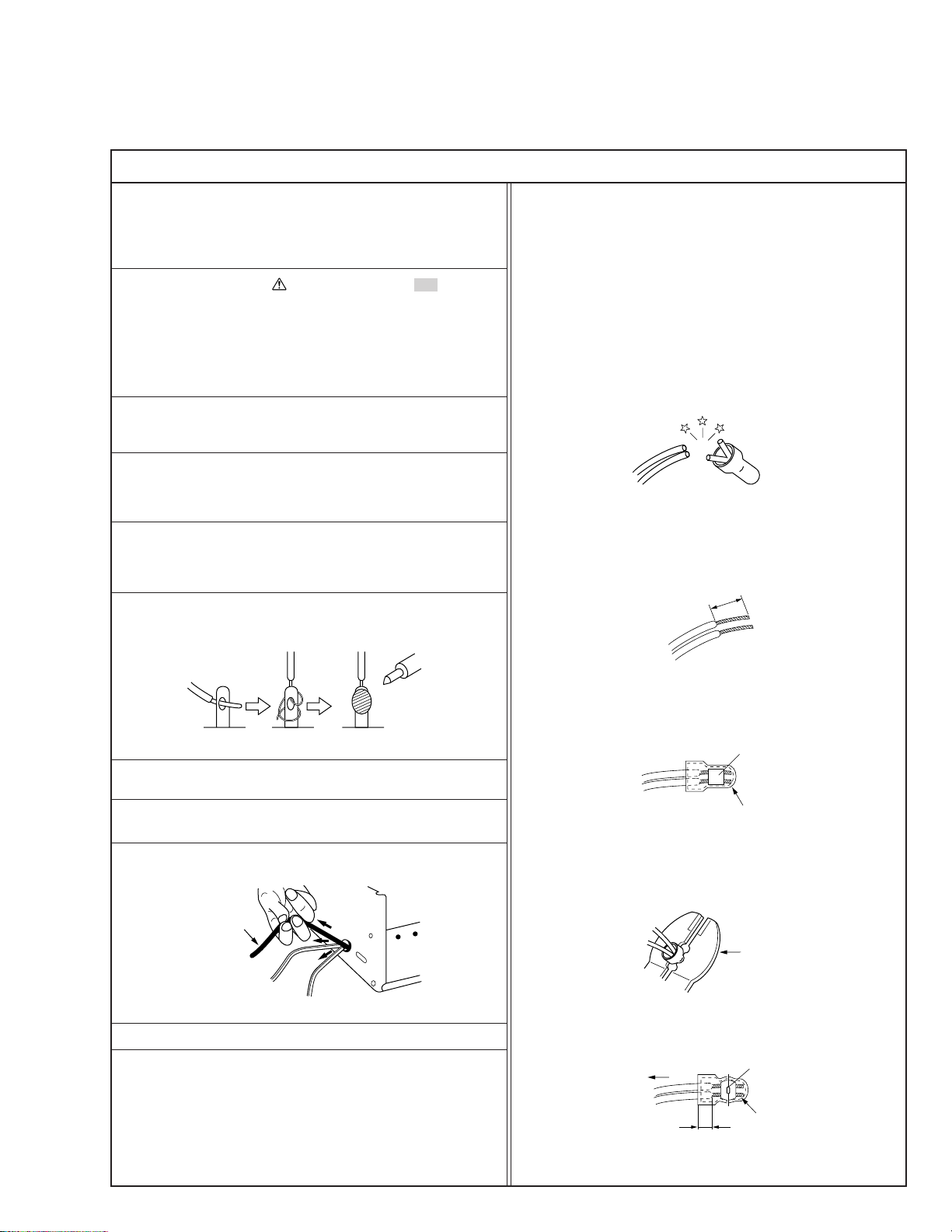
symbol and shaded ( ) parts are
12. Crimp type wire connector
In such cases as when replacing the power transformer in sets
where the connections between the power cord and power
transformer primary lead wires are performed using crimp type
connectors, if replacing the connectors is unavoidable, in order to prevent safety hazards, perform carefully and precisely
according to the following steps.
1) Connector part number : E03830-001
2) Required tool : Connector crimping tool of the proper type
which will not damage insulated parts.
3) Replacement procedure
(1) Remove the old connector by cutting the wires at a point
close to the connector.
Important : Do not reuse a connector (discard it).
cut close to connector
Fig.3
(2) Strip about 15 mm of the insulation from the ends of
the wires. If the wires are stranded, twist the strands to
avoid frayed conductors.
15 mm
7. Observe that wires do not contact heat producing parts
8. Check that replaced wires do not contact sharp edged or
9. When a power cord has been replaced, check that 10-15 kg of
10. Also check areas surrounding repaired locations.
11. Products using cathode ray tubes (CRTs)
Fig.1
(heatsinks, oxide metal film resistors, fusible resistors, etc.)
pointed parts.
force in any direction will not loosen it.
Power cord
Fig.2
In regard to such products, the cathode ray tubes themselves,
the high voltage circuits, and related circuits are specified for
compliance with recognized codes pertaining to X-ray emission.
Consequently, when servicing these products, replace the cathode ray tubes and other parts with only the specified parts.
Under no circumstances attempt to modify these circuits.
Unauthorized modification can increase the high voltage value
and cause X-ray emission from the cathode ray tube.
Fig.4
(3) Align the lengths of the wires to be connected. Insert
the wires fully into the connector.
Fig.5
(4) As shown in Fig.6, use the crimping tool to crimp the
metal sleeve at the center position. Be sure to crimp fully
to the complete closure of the tool.
1.25
2.0
5.5
Fig.6
(5) Check the four points noted in Fig.7.
Not easily pulled free
Wire insulation recessed
more than 4 mm
Fig.7
Crimping tool
Crimped at approx. center
of metal sleeve
Conductors extended
1
Page 5
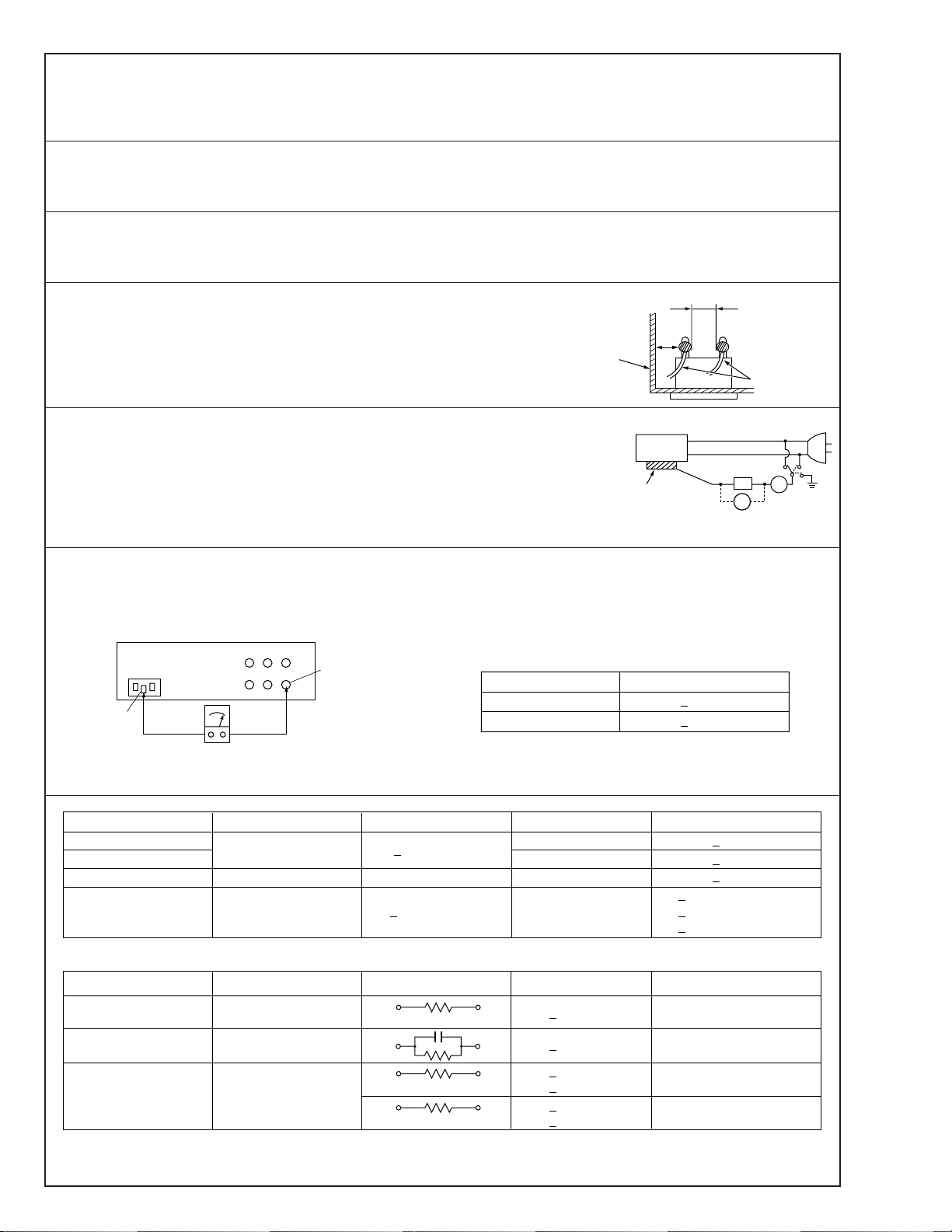
p
Safety Check after Servicing
Examine the area surrounding the repaired location for damage or deterioration. Observe that screws, parts and wires have been
returned to original positions, Afterwards, perform the following tests and confirm the specified values in order to verify compliance with safety standards.
1. Insulation resistance test
Confirm the specified insulation resistance or greater between power cord plug prongs and
externally exposed parts of the set (RF terminals, antenna terminals, video and audio input
and output terminals, microphone jacks, earphone jacks, etc.). See table 1 below.
2. Dielectric strength test
Confirm specified dielectric strength or greater between power cord plug prongs and exposed
accessible parts of the set (RF terminals, antenna terminals, video and audio input and output
terminals, microphone jacks, earphone jacks, etc.). See table 1 below.
3. Clearance distance
When replacing primary circuit components, confirm specified clearance distance (d), (d’) between soldered terminals, and between terminals and surrounding metallic parts. See table 1
below.
Chassis
Fig. 8
4. Leakage current test
Confirm specified or lower leakage current between earth ground/power cord plug prongs
and externally exposed accessible parts (RF terminals, antenna terminals, video and audio
input and output terminals, microphone jacks, earphone jacks, etc.).
Measuring Method : (Power ON)
Insert load Z between earth ground/power cord plug prongs and externally exposed accessible parts. Use an AC voltmeter to measure across both terminals of load Z. See figure 9 and
following table 2.
5. Grounding (Class 1 model only)
Confirm specified or lower grounding impedance between earth pin in AC inlet and externally exposed accessible parts (Video in,
Video out, Audio in, Audio out or Fixing screw etc.).
Measuring Method:
Connect milli ohm meter between earth pin in AC inlet and exposed accessible parts. See figure 10 and grounding specifications.
AC inlet
Earth pin
Exposed accessible part
Grounding Specifications
Region
USA & Canada
Europe & Australia
Externally
exposed
accessible
Grounding Impedance (Z)
d
d'
art
≤
Z 0.1 ohm
≤
Z 0.5 ohm
Power cord,
primary wire
Z
V
Fig. 9
ab
c
A
Milli ohm meter
Fig. 10
AC Line Voltage
100 V
100 to 240 V
110 to 130 V
110 to 130 V
200 to 240 V
100 V
110 to 130 V
110 to 130 V
220 to 240 V
Note: These tables are unofficial and for reference only. Be sure to confirm the precise values for your particular country and locality.
Region
Japan R 1 MΩ/500 V DC
USA & Canada
Europe & Australia R 10 MΩ/500 V DC
Region Load Z
Japan
USA & Canada
Europe & Australia
Table 2 Leakage current specifications for each region
Insulation Resistance (R)
≤
–
≤
Table 1 Specifications for each region
1 kΩ
0.15 µF
1.5 kΩ
2 kΩ
50 kΩ
Dielectric Strength
AC 1 kV 1 minute
AC 1.5 kV 1 miute
AC 900 V 1 minute
AC 3 kV 1 minute
AC 1.5 kV 1 minute
i1 mA rms Exposed accessible parts
i 0.5 mA rms
i 0.7 mA peak
i2 mA dc
i 0.7 mA peak
i2 mA dc
≤
≤
≤
≤
≤
≤
(Class 2)
(Class 1)
Clearance Distance (d), (d')
≤
d, d' 3 mm
≤
d, d' 4 mm
≤
d, d' 3.2 mm
≤
d 4 mm
≤
d' 8 mm (Power cord)
≤
d' 6 mm (Primary wire)
a, b, cLeakage Current (i)AC Line Voltage
Exposed accessible parts
Antenna earth terminals
Other terminals
2
Page 6
SECTION 1
3
4
SERVICE CAUTIONS AND DISASSEMBLY
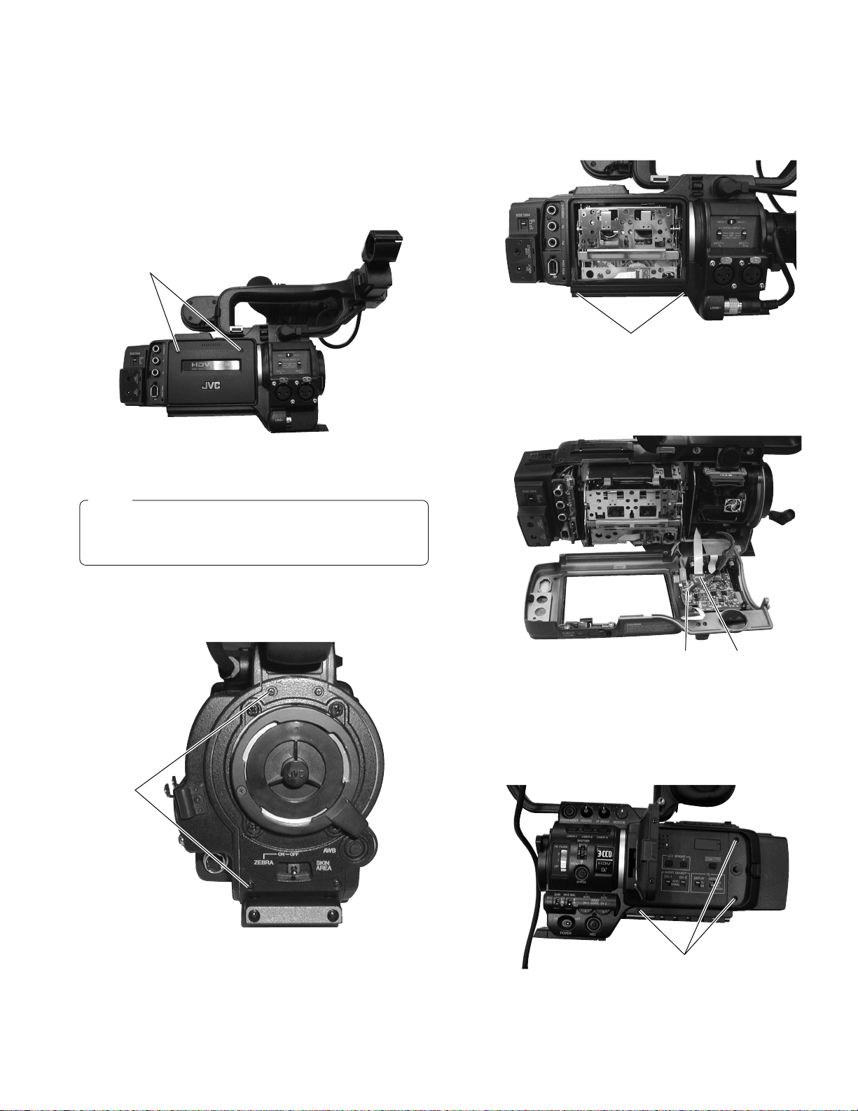
1.1 HOW TO REMOVE THE COSMETIC PARTS
1.1.1 Left side cover
(1) Remove the two screws
ward and pull out to remove.
, slide the cassette cover down-
1
1
Fig. 1.1.1 (1)
Note :
When attaching the cassette cover, make sure to insert the
hook of the cassette cover to the correct position of the
cassette housing.
(3) Remove the two screws
(4) Disconnect the cables CN13 and CN43.
and open the left side cover.
3
Fig. 1.1.1 (3)
(2) Remove the two screws
2
Fig. 1.1.1 (2)
2
.
CN13CN43
Fig. 1.1.1 (4)
1.1.2 Right side cover
(1) Remove the five screws 4 and open the right side cover.
Fig. 1.1.2 (1)
1-1
Page 7
1.2 HOW TO REMOVE THE OPTICAL BLOCK ASSEMBLY
CAUTION
When removing/mounting the optical block assembly in the
camera, take care not to damage cables, also the positioning of the wire assembly is important. A malfunction may
occur if a wire is somehow caught up.
4
Fig. 1.1.2 (2)
(2) Disconnect the cables CN14, CN24 and CN43 on AUDIO
board, CN10 and CN52 on STA board, CN52 on SWP board.
(1) Remove left side cover and the right side cover. (see sec-
tion 1.1.1 and 1.1.2)
(2) Remove the two screws
and remove the FAN motor.
1
1
Fig. 1.2 (1)
(3) Remove the two screws
(4) Disconnect the cables CN26, CN27 and CN28.
CN26 CN27
2
and remove the SD board.
2
1-2
CN52 CN10 CN43 CN24 CN14
Fig. 1.1.2 (3)
CN28
Fig. 1.2 (2)
Page 8
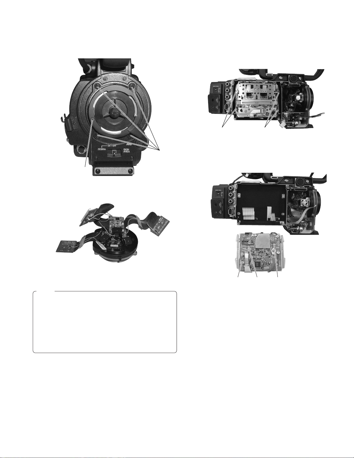
(5) Remove the five screws 3 3 and 4 , then remove the opti-
11
CN16CN75 CN17
cal block assembly carefully not to damage boards and cables.
3
4
Fig. 1.2 (3)
1.3 HOW TO REMOVE VCR UNIT
1.3.1 Mechanism unit
(1) Remove the left side cover. (see section 1.1.1)
(2) Remove the four screws
(3) Lift up the mechanism unit gently and disconnect the
cablesCN75, CN16 and CN17.
.
1
Fig. 1.3.1(1)
Fig. 1.2 (4)
Note :
• The CCDs are bonded precisely to the prism. In case of
trouble with a CCD, it is not possible to replace an individual CCD, but the entire optical block assembly should
be replaced.
• The optical block assembly supplied as a service part.
• When replacing the optical block, attach the original FAN
and FNC board to the new optical block because those
are not included on the optical block assembly.
Fig. 1.3.1(2)
1-3
Page 9
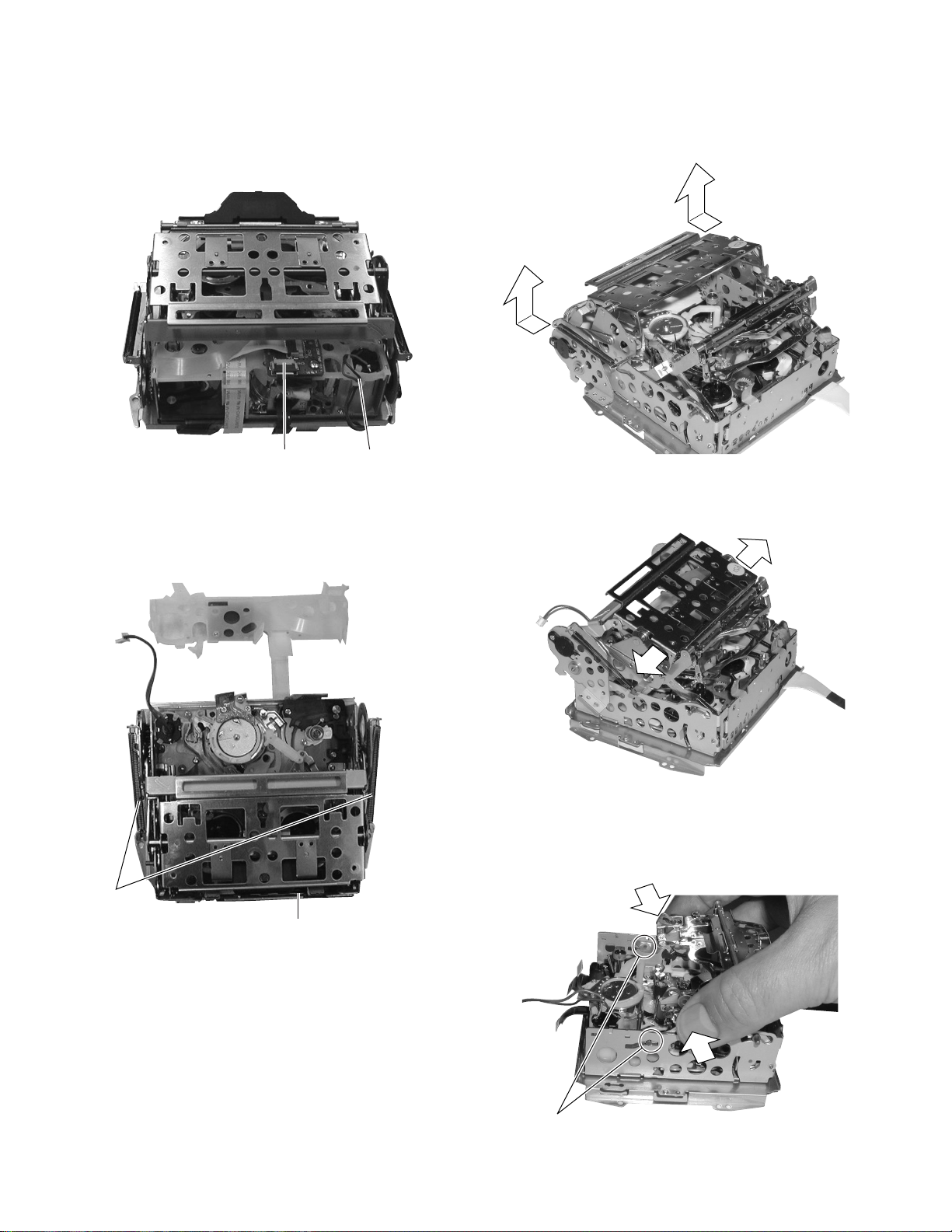
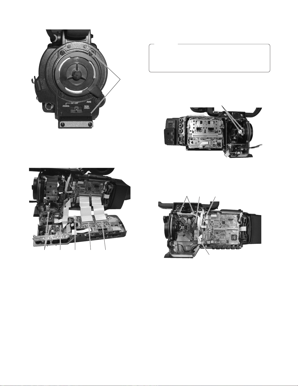
1.3.2 Cassette housing
(1) Remove the mechanism unit. (see section 1.3.1)
(2) Remove CN1 and release the motor wire. Release the lock
sideways and remove the tape guard
CN1 Motor Wire
(4) Slide the outer unit to rear direction and lift up slightly. Pull
out to side direction to release the outer unit. Perform same
manner other side.
Fig. 1.3.2(1)
(3) Pop up the cassette housing by sliding release lever and
remove the two screws
2
.
2
Release Lever
Fig. 1.3.2(3)
Fig. 1.3.2(4)
(5) Slide the cassette housing to the position of fig.1.3.2(5) and
hold the cassette housing slightly to inside direction to release it.
1-4
Fig. 1.3.2(2)
Release Position
Fig. 1.3.2(5)
Page 10
(6) Release bosses of the cassette housing from the mecha-
nism unit.
Fig. 1.4.1(2)
Fig. 1.3.2(6)
1.4 HOW TO REMOVE THE MAJOR BOARDS
1.4.1 Audio board
(1) Remove right side cover. (see section 1.1.2)
(2) Disconnect cables CN44, CN45 and CN62.
(3) Remove six screws
and 2.
1
1
1
Fig. 1.4.1(1)
2
1.4.2 LCD monitor
(1) Remove Audio board. (see section 1.4.1)
(2) Remove two screws
3
.
3
Fig. 1.4.2(1)
(3) Remove the hinge cover and remove two screws
Hinge Cover
4
4
.
Note :
CN62 may be slightly hard to connect FPC cable. Make sure
to insert the cable to correct position.
Fig. 1.4.2(2)
1-5
Page 11
1.4.3 MIF board
(1) Remove the right side cover. (see section 1.1.2)
(2) Remove four screws
(3) Remove the cables CN4, CN9, CN11, CN12, CN13, CN22,
CN23, 34 and CN48, then lift up MIF board to release B to B
connector between MIF board and MAIN board.
5
.
(4) Slide the MAIN board downward and pull out.
Do not bend the Heat Pipe.
Do not bend the Heat Pipe.
CN12CN13 CN23
CN22CN48
5
CN4
CN34
CN11
CN9
5
Fig. 1.4.3
1.4.4 MAIN board
(1) Remove MIF board. (see section 1.4.3)
(2) Remove six screws 6 and 7.
(3) Remove the cables CN3, CN16, CN17, CN18, CN19, CN26,
CN27, CN28, CN29 and CN30.
7
6
Fig. 1.4.4(2)
(5) Remove the two screws 8. Remove the heat sink carefully
because it is being fitted sticky.
8
CN26
CN27
CN28
CN17CN18 CN3 CN16
Fig. 1.4.4(1)
CN29
CN30
CN19
Fig. 1.4.4(3)
1.4.5 HANDLE assembly
(1) Remove left side cover and right side cover. (see section
1.1.1 and 1.1.2)
(2) Remove two screws
9
.
9
1-6
Fig. 1.4.5(1)
Page 12
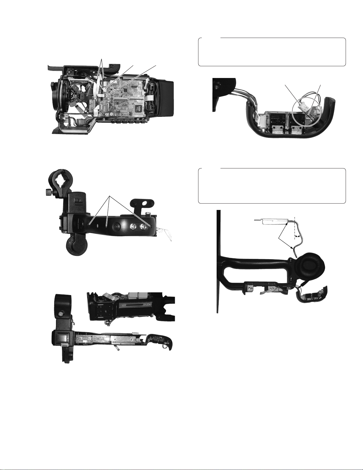
Longer PinRed wire
(3) Remove the cables CN12 and CN48. Remove the two screws
and lift up the handle assembly.
0
0
CN12 CN48
Fig. 1.4.5(2)
(4) Remove three screws
!
.
!
Note :
When connecting the LED connector on EAR board, ensure the polarity that the red wire should be connected
longer pin of LED.
Fig. 1.4.5(5)
Note :
When removing the Heat Sink Ass’y, bend the Heat Pipe
slightly like Fig. 1.4.5(6).
Return the bend after attaching the Heat Sink Ass’y.
Do not bend the other portion of Heat Pipe.
Fig. 1.4.5(3)
(5) Remove the handle cover R and handle cover T.
Fig. 1.4.5(4)
Do not bend
Fig. 1.4.5(6)
About
20 degrees
1-7
Page 13
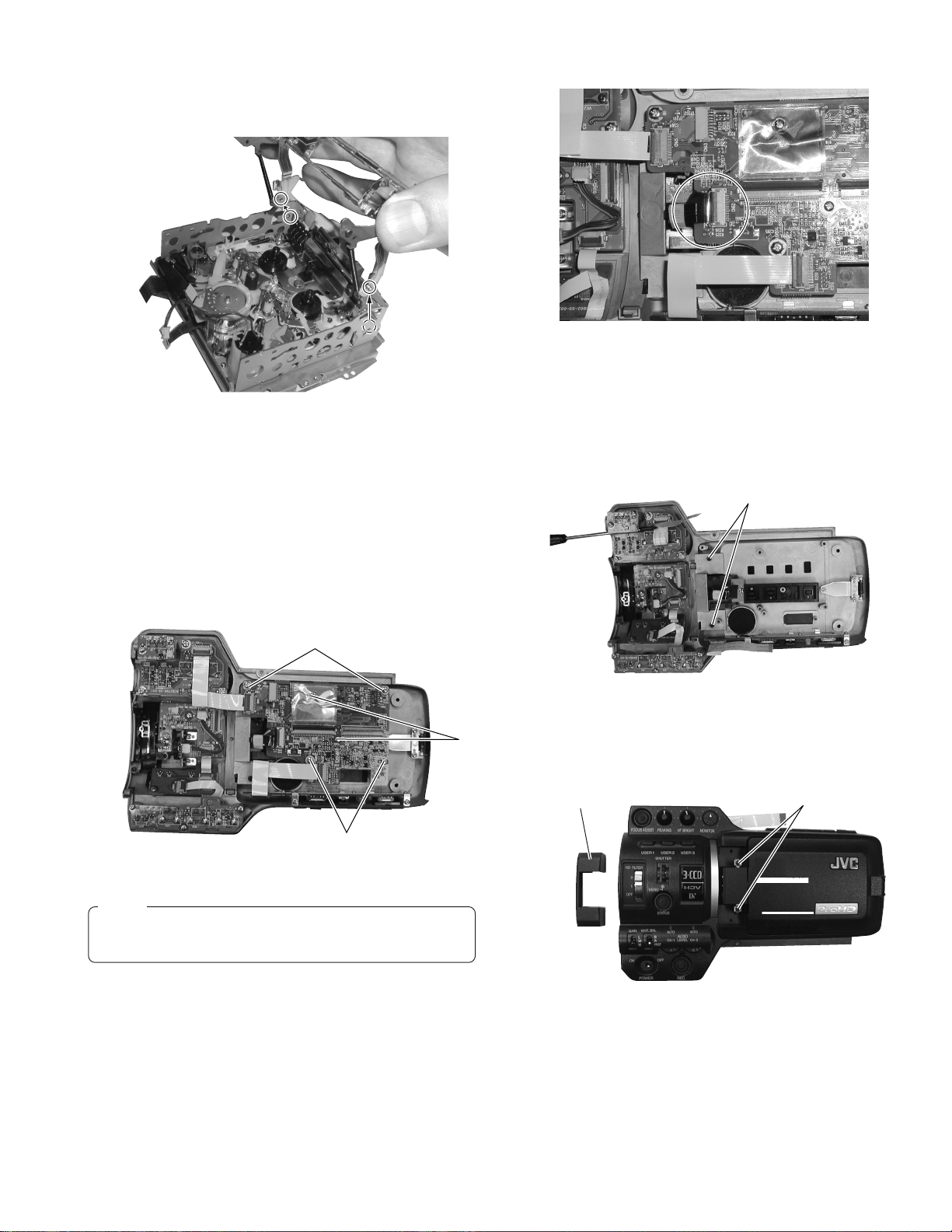
1.4.6 PS board
(1) Remove the four screws
Fig. 1.4.6(1)
(2) Remove the four screws
CN1, 29, CN30, CN53 and CN75.
.
@
@@
and $. Disconnect the cables
#
CN30
CN29
CN75
$
1.5 SERVICE MENUS
1.5.1 Modes required in servicing
(1) While holding down the specified button(s) (FOCUS ASSIST,
USER 3), press and hold the STATUS button for more than
1 second in order to display the first-level menu of the service menu hierarchy. The items in the first-level menu vary
according to which specified button is being held at the moment the STATUS button is pressed. (Characters are displayed on LCD monitor screen or View finder.)
When power up
Item Displayed Content
CAMERA1 MENU
CAMERA2 MENU
CAMERA3 MENU
VTR1 MENU
VTR2 MENU
VTR3 MENU
DIP SW
HOUR METER
ERROR HISTORY
OTHERS
VERSION
Camera setting, blemish detect
Error correct ON/OFF
AW data reset menu
Repeat, FF/REW speed setting
Long pause, shutdown setting
Reserved, BATT, Info.
DIP SW MENU
Hour Meter indication
Error History
MENU SAVE etc.
CPU Version indication
Holding
ⳮ
DISPLAY
button
Activation Method
FOCUS
USER 3
ASSIST
嘷
ⳮ
ⳮ
嘷
ⳮ
ⳮ
ⳮ
ⳮ
ⳮ
ⳮ
嘷
Holding
DISPLAY
button
FOCUS ASSIST
USER 3
嘷
嘷
ⳮ
嘷
嘷
ⳮ
嘷
嘷
嘷
嘷
ⳮ
+
嘷
嘷
嘷
嘷
嘷
嘷
嘷
嘷
嘷
嘷
ⳮ
Table 1-5-1 Service Menu First Tier List
CN1
CN53
#
Fig. 1.4.6(2)
Note :
When replacing the fuse F1, ensure to replace with same
type fuse. (refer to the parts list)
1.5.2 Operation in the first-level of the service menu
(1) While holding down the specified button(s) (FOCUS ASSIST
or USER 3), press and hold the STATUS button for more
than 1 second.
(2) The first-level of the service menu is displayed.
(3) Rotate the SHUTTER dial to move the cursor ( 3) on to the
item to be modified.
(4) Push into the SHUTTER dial to direct the item on which the
cursor ( 3) is located.
• Pressing the STATUS button returns to the MENU display.
• Can not open the service MENU while recording.
– – – A DV A NC E D M EN U – – –
V ERS ION CHECK . .
CAMERA 1 . .
VTR1 . .
EX I T
Fig. 1-5-2 (1)
While holding down the FOCUS ASSIST button, press and
hold STATUS button for more than 1 second,this MENU
screen is shown on the monitor. (Refer to Fig. 1-5-2(1))
1-8
Page 14
– – – S ER V I C EMENU–––
OFF When the face of LCD screen is
turned toward the camera subject,
does not invert the left and right of
the LCD display. (normal image)
ON When the face of LCD screen is
turned toward the camera subject,
inverts the left and right of the LCD
display. (mirror image)
AUTO When selected FAS mode, audio
recording Level will be
automatically set to AUTO mode.
SW SET When selected FAS mode, audio
recording level will be depending
on switch setting.
ALC + EEI
When selected ALC mode
including FAS mode, EEI function
will be activated.
ONLY ALC
When selected ALC mode
including FAS mode, EEI function
will not be activated.
U MODEL
1/240 Maximum shutter speed is
set to 1/240 second.
1/480 Maximum shutter speed is
set to 1/480 second.
1/960 Maximum shutter speed is
set to 1/960 second.
E MODEL
1/200 Maximum shutter speed is
set to 1/200 second.
1/400 Maximum shutter speed is
set to 1/400 second.
1/800 Maximum shutter speed is
set to 1/800 second.
OFF When selected FULL AUTO mode,
IRIS mode will be depeng on IRIS
MODE switch of the lens.
ON When selected FULL AUTO mode,
Auto Iris mode will be activated
even Manual Iris mode is selected.
CANCEL Does not execute blemish
detection.
EXECUTE
Execute blemish detection.
Item Parameter
LCD L/R
REVERSE
FAS
AUDIO
ALC MODE
EEI MAX
( indicates the factory setting.)
PIXEL
COMPEN DET
IRIS ENF.
AUTO
CAMERA 1 . .
CAMERA 2 . .
VTR1 . .
VTR2 . .
DIP S
HOUR ME T E R
ERROR H I STORY . .
OTHERS . .
EX I T
At first, while holding down the DISPLAY button, turn ON
the power switch, and then, while holding down the USER
3 button, press and hold STATUS button for more than 1
second, this MENU screen is shown on the monitor. (Refer
to Fig. 1-5-2(2))
– – – F A C T O R YMENU–––
CAMERA 1 . .
CAMERA 2 . .
CAMERA 3 . .
VTR1 . .
VTR2 . .
VTR3 . .
DIP S
HOUR ME T E R
ERROR H I STORY . .
At first, while holding down the DISPLAY button, turn ON
the power switch, and then, While holding down the FOCUS ASSIST and USER 3 button, press and hold STATUS
button for more than 1 second, this MENU screen is shown
on the monitor. (Refer to Fig. 1-5-2(3))
1.5.3 CAMERA 1 menu
(1) In a service menu, place the cursor ( 3) on “CAMERA 1”
and push the SHUTTER dial to display the CAMERA1 menu.
OTHERS . .
EX I T
LCD L / R REVERSE OFF
FAS AUD IO AUTO
ALC MODE ALC+EEI
EE I MAX 1 / 2 40
IRIS ENF AUTO ON
PIXEL COMPEN DET CANCEL
P AGE BACK
(2) Rotate the SHUTTER dial to move the cursor ( 3) on the
mode to be adjusted.
(3) Push the SHUTTER dial so that the parameter blinks.
(4) Rotate the SHUTTER dial to vary the parameter.
(5) After completing the parameter setting, push the SHUTTER
dial to stop the blinking of the parameter and store the set-
ting in memory.
(6) After completing the setting, move the cursor ( 3) to “PAGE
BACK” and push the SHUTTER dial to return to the display
at the higher hierarchy level.
W
..
Fig. 1-5-2 (2)
W
..
Fig. 1-5-2 (3)
– – – C AM ER A 1 – – –
Fig. 1-5-3 (1)
Table 1-5-3 (1)
䡵 White blemish detection
Open the User MENU, select "VIDEO FORMAT", "REC", set
to "HDV-HD24P" and push the SHUTTER dial.
Select "FRAME RATE", set to "24" and push the SHUTTER
dial. Select "EXECUTE", push the SHUTTER dial, then GYHD100 is automatically rebooted.
– – – V I D EO F OR M A T – – –
FRAME RATE 24
REC HDV - HD 2 4 P
ASPECT - - - PB OUTPUT 7 2 0P
PB T APE DVCAM
OUT P UT T ERM I NA L COMPOS I T E
SET UP 0 . 0
P AGE BACK
EXECUTE
EXECUTE
%
Fig. 1-5-3 (2)
1-9
Page 15
Open the Service MENU, select "CAMERA1", "PIXEL
COMPEN DET", "EXECUTE" and push the SHUTTER dial, then
CCD white blemish detect operation start automatically.
At this time, the lens is closed and the camera is in the SLOW
SHUTTER
mode.
– – – C AME RA 1 – – –
LCD L / R REVERSE OFF
FAS AUD IO AUTO
ALC MODE ALC+EE I
EE I MAX 1/240
IRIS ENF AUTO ON
PIXEL COMPENDET EXECUI T
P AGE BACK
Fig. 1-5-3 (3)
䡵 Details on correctable white blemish
Up to 127 errors with composite video levels of 50mV or
more can be corrected. No limitation of errors per line within
127 however, the maximum consecutive errors are 4 and
the correction results may be inferior to the case of single
error correction.
Oblique noise may be observed on the screen during white
blemish detection. This is due to the principles of error correction and is not a malfunction.
White blemish can be detected in the following area.
100%
After completing white blemish detection, return "REC" and
"FRAME RATE" setting to original one's.
When the white blemish detection completes, the result data
is stored in the memory of CPU,
end message is shown as below, then please turn off.
PIXEL COMPEN
END
TURN PO
AND ON AGA I N
W
ER OFF
Fig. 1-5-3 (4)
If any errors occurs during the detection operation, an error message is displayed , and return to MENU display.
Message TreatmentError details
LENS NOT
CLOSED?
COUNT OVER
The lens does not
close for detection.
The number exceeds
the specified count.
No result is stored in
the EEPROM.
Only the specified
count of data is
stored in the
EEPROM.
Table 1-5-3 (2)
100%
Fig. 1-5-3 (5)
1.5.4 CAMERA 2 menu
(1) In a service menu, place the cursor on “CAMERA 2” and
push the SHUTTER dial to display the CAMERA2 menu.
– – – C A MERA2 – – –
PIXEL COMPE N ON
TEST S I GNAL OFF
P AGE BACK
Fig. 1-5-4
Operation ways are almost same as CAMERA 1 MENU, so
please refer it.
Item Parameter
PIXEL
COMPEN *1
OFF Does not correct the detected white
blemish.
ON Corrects the detected white blemish.
CHECK
Light up the pixels which are the
detected white blemish.
( indicates the factory setting.)
Table 1-5-4
1-10
*1: This mode is automatically set to ON when the power
is turned on.
The OFF mode is enabled only after it is set to OFF at
this screen until the power is turned off.
Page 16
1.5.5 CAMERA 3 menu
OFF Does not indicate the Battery
information.
AUTO Show the Battery information as
Battery Info of VTR3 MENU.
OFF Disable repeat recording
2 Perform repeat recording 2 times.
5 Perform repeat recording 5 times.
12 Perform repeat recording 12 times.
ON Enable full repeat recording.
OFF Disable repeat playback.
ON Enable repeat playback.
FF/REW When FF/REW command is
received from REMOTE, it runs as
FF/REW mode.
SEARCH When FF/REW command is
received from REMOTE, it runs as
search FWD/REV mode.
FIELD
FRAME
X5 Maximum FF/REW speed is limited up
to x5.
X7.5 Maximum FF/REW speed is limited up
to x7.5.
X10 Maximum FF/REW speed is limited up
to x10.
MAX *1No limitation
DV Horizontal effective pixels are 720.
STANDARD Horizontal effective pixels are
710 at 60/30 frame rate and 702 at
50/25 frame rate.
Item Parameter
BATT.
DISPLAY
REC REPEAT
PLAY REPEAT
REMOTE
FF/REW
STEP
SLOW [DV]
FF/REW
SPEED
VIDEO OUT
HBLANK
( indicates the factory setting.)
In a service menu, place the cursor on “CAMERA 3” and push
the SHUTTER dial to display the CAMERA3 menu.
Operation ways are almost same as CAMERA 1 MENU, so
please refer it.
Item Parameter
AW/SKIN RESET
PIXEL COMP
RESET
CCD ADJ
RESET
CAM EEPROM
RESET
– – – C A ME R A 3 – – –
W
/SKIN RESET CANCEL
A
PIXEL COMP RESET CANCEL
CCD A D J RES E TCANCEL
CAN EE PROM RESET CANCEL
P AGE BACK
Fig. 1-5-5
CANCEL Does not reset the auto white
EXECUTE Resets the auto white data and
CANCEL Does not reset the detected white
EXECUTE Resets the detected white
CANCEL Does not reset the CCD
EXECUTE Resets the CCD adjustment data.
CANCEL Does not reset the EEPROM data
EXECUTE Resets the EEPROM data for
data and the skin detect data.
the skin detect data.
blemish data.
blemish data.
adjustment data.
for CAMERA CPU.
CAMERA CPU.
( indicates the factory setting.)
Table 1-5-5
1.5.6 VTR 1 menu
In a service menu, place the cursor on “VTR 1” and push the
SHUTTER dial to display the VTR 1 menu.
––– VTR1–– –
BATT . D I SPL AY AUTO
REC REPE AT OF F
PLAY REPEAT OFF
REMOTE FF /RE
STEP SLOW[DV] FRAME
FF / RE
W
VIDEO OUT HBLANK DV
P AGE BACK
W
FF / RE
SPEED MAX
W
Fig. 1-5-6
Operation ways are almost same as CAMERA 1 MENU, so
please refer it.
Table 1-5-6
*1: Maximum speed is x20 at VTR mode, but no function
at CAM mode.
1-11
Page 17
0 Normal setting
Refer to next page.
Item Parameter
RESERVED
BATTERY INFO
( indicates the factory setting.)
1.5.7 VTR 2 menu
In a service menu, place the cursor on “VTR 2” and push the
SHUTTER dial to display the VTR 2 menu.
1.5.8 VTR 3 menu
In a service menu, place the cursor on “VTR 3” and push the
SHUTTER dial to display the VTR 3 menu.
––– VTR2–– –
L ONG PAUSE ON
BATT . SHUT DO
B ATY.ALARM 6.9V
ANTON SHUT DO
ANTON ALARM 13 . 5V
DF MASK [ DV ] OFF
P AGE BACK
W
N6.0V
W
N12.6V
Fig. 1-5-7
Operation ways are almost same as CAMERA 1 MENU, so
please refer it.
Item Parameter
LONG PAUSE
OFF Disable the long pause function.
ON Enable the long pause function.
BATT.
SHUTDOWN *1
BATT.
ALARM *1
ANTON SHUT
DOWN
6.8V Setting of the battery voltage when
shutdown should occur. (Setting in
0.1V steps between 6.3V and 7.5V.)
6.9V Setting of the battery voltage when
battery alarm is indicated. (Setting in
0.1 V steps between 6.3V and 8.0V.)
12.0V Setting of the ANTON battery voltage
when shutdown should occur. (Setting
in 0.1V steps between 10.5V and
13.6V.)
ANTON
ALARM
13.5V Setting of the ANTON battery voltage
when battery alarm is indicated.
(Setting in 0.1 V steps between 10.5V
and 13.6V.)
DV DF MASK *2
OFF "1" is recorded as per format.
ON "0" is always recorded.
( indicates the factory setting.)
Table 1-5-7
––– VTR3–– –
RESERVD 0
BATTELY I NFO . .
PAG BACK
Fig. 1-5-8 (1)
Changing of setting is prohibited.
Table 1-5-8 (1)
䡵 BATTERY INFO Display
Display method
Move the cursor to the “BATTERY INFO..” in “VTR3” screen
and press SHUTTER dial. BATTERY INFO screen (right figure) will be displayed.
– – – B A T T E R Y I N F O – – –
T YPE ANTON SMART
R EMA I N 1 2 5M i n / 9 5
<12.8V 1.25A 30° C>
FUL L CAPACI TY 3 2 . 6Ah
PRESENT CAPAC I TY 3 0 . 5 A h
SER I A L NO. 5 5 5 2 0
MANU F AC T UR E2004/04
SOF TWARE REV . 1 2 . 5
CAL I BRAT I ON REQU I RED OFF
P AGE BACK
%
*1 : When operating by DC input, then “SHUT DOWN” will be
set to 6.0V, and “ALARM” will be set to 6.9V automatically, and these setting will not relate to menu setting.
*2 : FRAME RATE 50/25 only
1-12
Fig.1-5-8 (2) BATTERY INFO
(When the Anton/Bauer Smart Battery is detected)
Page 18
Item Descriptions
TYPE
ANTON SMART When ANTON/BAUER SMART BATTERY is connected
AFG When BATTERY with I/F of AFG (AnalogFuelGauge) is connected
OTHERS When other BATTERY is connected
NO DETECT When no BATTERY is connected
REMAIN Minute
%
Voltage
Current
Temperature
FULL CAPACITY
PRESENT CAPACITY
SERIAL NO.
MANUFACTURE
SOFTWARE REV.
CALIBRATION
REQUIRED
Remaining battery lasting time [min] calculated based on current power consumption
Current remaining capacity [%] corresponding to total battery capacity
Output voltage of battery
Output current of battery
Temperature of battery
Capacity [Ah] when the BATTERY is fully charged
Current BATTERY capacity [Ah]
Manufactured serial number
Manufactured date
Software revision number
OFF Calibration not required
ON Calibration required
Table 1-5-8 (2)
1.5.9 DIP SW menu
(1) In a service menu, place the cursor on “DIP SW ” and push the SHUTTER dial to display the DIP SW menu.
– – – D I P SW [ 1 / 6 ] – – –
W
ALL RESET CANCEL
DIPS
NEXT PAGE
P AGE BACK
Fig. 1-5-9 (1)
– – – D I P SW [ 4 / 6 ] – – –
W
16 OFF
DIPS
DIPS
W
17 OFF
DIPS
W
18 OFF
W
19 OFF
DIPS
DIPS
W
20 OFF
DIPS
W
21 OFF
DIPS
W
22 OFF
DIPSW23 OFF
NEXT PAGE
P AGE BACK
Fig. 1-5-9 (4)
– – – D I P SW [ 2 / 6 ] – – –
W
00
DIPS
DIPS
W
1OFF
DIPS
W
2OFF
W
3OFF
DIPS
DIPS
W
4OFF
DIPS
W
5OFF
DIPS
W
6OFF
DIPSW7OFF
NEXT PAGE
P AGE BACK
Fig. 1-5-9 (2)
– – – D I P SW [ 5 / 6 ] – – –
W
24 OFF
DIPS
DIPS
W
25 OFF
DIPS
W
26 OFF
W
27 OFF
DIPS
DIPS
W
28 OFF
DIPS
W
29 OFF
DIPS
W
30 OFF
DIPSW31 OFF
NEXT PAGE
P AGE BACK
Fig. 1-5-9 (5)
– – – D I P SW [ 3 / 6 ] – – –
W
8OFF
DIPS
DIPS
W
9OFF
DIPS
W
10 OFF
W
11 OFF
DIPS
DIPS
W
12 OFF
DIPS
W
13 OFF
DIPS
W
14 OFF
DIPSW15 OFF
NEXT PAGE
P AGE BACK
Fig. 1-5-9 (3)
– – – D I P SW [ 6 / 6 ] – – –
W
32 0
DIPS
DIPS
W
33 0
DIPS
W
34 0
W
35 OFF
DIPS
DIPS
W
36 OFF
DIPS
W
37 OFF
DIPS
W
38 OFF
DIPSW39 OFF
P AGE BACK
Fig. 1-5-9 (6)
1-13
Page 19
Operation ways are almost same as CAMERA 1 menu, so please
--- DIP SW 6/6 --0
0
0
OFF
OFF
OFF
OFF
OFF
DIP SW 32
DIP SW 33
DIP SW 34
DIP SW 35
DIP SW 36
DIP SW 37
DIP SW 38
DIP SW 39
Change prohibited
Change prohibited
Change prohibited
Change prohibited
Change prohibited
Change prohibited
Change prohibited
Change prohibited
gp
refer it.
All DIP Switch settings which are shown below should
not be changed ecxept for repair or maintenance. And
do not forget to return original position after repair.
Item Parameter
--- DIP SW 1/6 ---
DIP SW
ALL
RESET
CANCEL Cancel to reset all
DIPSW settings.
EXECUTE Execute to reset all
DIPSW settings.
--- DIP SW 2/6 ---
DIP SW 0
1:Displays error rate monitor
and CPU port information
DIP SW 1
ON : Disable warning message
display
DIP SW 2
DIP SW 3
DIP SW 4
DIP SW 5
DIP SW 6
DIP SW 7
Change prohibited
ON : Disable DEW warning
Change prohibited
Change prohibited
Change prohibited
Change prohibited
--- DIP SW 3/6 ---
DIP SW 8
DIP SW 9
DIP SW 10
Change prohibited
Change prohibited
ON :
Displays error rate solely
for audio block on the error rate
monitor screen
DIP SW 11
DIP SW 12
DIP SW 13
DIP SW 14
DIP SW 15
Change prohibited
Change prohibited
Change prohibited
Change prohibited
Change prohibited
Factory
setting
CANCEL
0
OFF
OFF
OFF
OFF
OFF
OFF
OFF
OFF
OFF
OFF
OFF
OFF
OFF
OFF
OFF
Table 1-5-9
ERROR RATE MONITOR screen
By setting "DIP SW 0" to "1", error rate and each CPU port information display screen will appear on the LCD monitor, View
finder and monitor.
The values which are pointed by arrow are the error rate value.
Error rate of CH-1 shown in upper row, and CH-2 shown in lower
row, and these value are indicated total AUDIO/VIDEO error rate.
When the error rate increase , the warning message "HEAD
CLEANING REQUIRED" is displayed. And this message is indicate when the error rate value is over 4,500 (one-channel AUDIO/VIDEO total) for 7 seconds consecutively.
ERROR RATE indicator
XXXX
65535 XX XX XX XX XX XX
65535 XX
FI L1
F5.68
STBY
XX
T
XX
D
XX XX XX
XX
XX XX XXXX
CHCH12---------+-+--
01/ 02/ 03 AM01: 23: 45
00: 00: 00: 00
XX XX XX
XX
--
SP 2 0 mir
ADP
FAS
-3 d B
XX
FA
12. 2V
W
I
SD
B
--- DIP SW 4/6 ---
DIP SW 16
DIP SW 17
DIP SW 18
DIP SW 19
DIP SW 20
DIP SW 21
DIP SW 22
DIP SW 23
--- DIP SW 5/6 ---
DIP SW 24
DIP SW 25
DIP SW 26
DIP SW 27
DIP SW 28
DIP SW 29
DIP SW 30
DIP SW 31
1-14
Change prohibited
Change prohibited
Change prohibited
Change prohibited
Change prohibited
Change prohibited
Change prohibited
Change prohibited
Change prohibited
Change prohibited
Change prohibited
Change prohibited
Change prohibited
Change prohibited
Change prohibited
Change prohibited
OFF
OFF
OFF
OFF
OFF
OFF
OFF
OFF
OFF
OFF
OFF
OFF
OFF
OFF
OFF
OFF
Fig. 1-5-9 (7)
Page 20
1.5.10 HOUR METER
In a service menu, place the cursor on “HOUR METER ” and
push the SHUTTER dial to display the HOUR METER menu.
– – – H O U R M ETER [ 1 / 2 ] – ––
DRUM CL E AR
TOTALDRUM 000000H
N
FA
PO
W
ER 000000H
C APSTAN 000000H
SEACH 000H00M
W
FF / RE
NEXT PAGE
P AGE BACK
000000H
000H00M
Fig. 1-5-10 (1)
– – – H O U R M ETER [ 2 / 2 ] –––
LOAD ING 0000000
EJECT 0000000
F
W
D/REV 0000000
CLEANING TAPE 0000000
P AGE BACK
Fig. 1-5-10 (2)
Operation ways are almost same as CAMERA 1 menu, so please refer it.
Item Parameter
DRUM
TOTAL DRUM
FAN
POWER
CAPSTAN
SEARCH
FF/REV
LOADING
EJECT
FWD/REV
CLEANING TAPE
000000 Displays the drum hour
meter(maintenance for drum)
CLEAR Resets the drum hour meter.
000000 Displays the total hour meter.
CLEAR Resets the total drum hour meter.
(This does not work unless the special
setting)
000000 Displays the fan hour meter.
CLEAR Resets the fan hour meter.
000000 Displays the power hour meter.
CLEAR Resets the power hour meter.
000000 Displays the capstan hour meter.
CLEAR Resets the capstan hour meter.
000000 Displays the search hour meter.
CLEAR Resets the search hour meter.
000000 Displays the FF/REW hour meter.
CLEAR Resets the FF/REW hour meter.
000000 Displays the loading count.
CLEAR Resets the loading count.
000000 Displays the eject count.
CLEAR Resets the eject count.
000000 Displays the forward/reverse
switching count.
CLEAR Resets the forward/reverse switching
count.
000000 Displays the cleaning tape working
count.
CLEAR Resets the cleaning tape working
count.
1.5.11 ERROR HISTORY
In a service menu, place the cursor on “ERROR HISTORY ” and
push the SHUTTER dial to display the ERROR HISTORY menu.
– – – E RR O R H ISTORY –––
(HISTORY - 1 ) 7101
CAP MOTOR FA I L URE
(HISTORY - 2 ) 7101
CAP MOTOR FA I L URE
(HISTORY - 3 ) 7101
CAP MOTOR FA I L URE
(HISTORY - 4 ) 7101
CAP MOTOR FA I L URE
CLEAR CANCEL
P AGE BACK
Fig. 1-5-11
(1) Rotate the SHUTTER dial to move the cursor onto the item
to show details.
(2) Push the SHUTTER dial so that the details of ERROR HIS-
TORY is shown.
(3) Rotate the SHUTTER dial to move cursor onto the “CLEAR”,
push the SHUTTER dial, then ERROR HISTORY will be deleted.
Note :
ERROR HISTORY was stored from “HISTORY-1” box to
“HISTORY-4”box. Latest error was stored “HISTORY-4”
box, and if there will be occur another error then latest error
history will be rewrite on “HISTORY-4”. From “HISTORY1” to “HISTORY-3” will not rewrite, except to “CLEAR”
operation.
1.5.12 Detail indication of ERROR HISTORY
In a ERROR HISTORY display, place a cursor onto the item and
push SHUTTER dial, then detail display (MECHANISM INFO)
picture will be shown.
MECHANISM INFO has 2 pages.
– – – M E CHAN I SM I NF 0 1 / 2 – –
P.TM 000000H
SYS MODE:PLAY(01. 00)
MSD MODE : P L A Y ( 0 1 . 00 )
LAST KEY:PLAY(01.00)
T APE REM[ 0 0 0 0 ]
DE
W
DIAMETER TU[00]SP[00]
NEXT PAGE
P AGE BACK
–>STOP( 00 . 00 )
[00] TEMP[00]
Fig. 1-5-12 (1)
– – – M E CHAN I SM I NF 0 2 / 2 – –
M.POSI BRK2FAST>BRK2FAST
H.POSI INI T >CASS IN
CAP [ OF F F
TU [ ON ] SP [ OFF ] DRM[ OFF ]
DRV [ 00 ] CAPV [ 0 0 ] RELV [ 00 ]
MCV [ 0 0 ] RE L I [ 0 0 ]
BGN [ OF F ] END [ ON ] CAS [ OFF ]
STD[OFF ] HW[OFF] HW2[OFF]
SPL [ OF F ] TH IN[ON]
P AGE BACK
W
D]REL [OFF FWD]
Table 1-5-10
Fig. 1-5-12 (2)
1-15
Page 21
Item Content Displayed Content
P.TM
SYS MODE
MSD MODE
LAST KEY
TAPE REM
DEW
TEMP
DIAMETER
M. POSI
CAP
REL
DRM
DIR
DRV
CAPV
RELV
POWER HOUR METER
SYSCON CPU mode when error occurred
PLAY (03, 00)
ParameterMODE DATA
MSD CPU mode and target mode when
error occurred
PLAY (01, 00)
ParameterMODE DATA
Final Key code when error occurred
PLAY (E7, 01)
ParameterMODE DATA
TAPE REMAIN
DEW sensor A/D intake value
Temperature sensor A/D intake value
The value “49” [5°C] is threshold of
detecting low temperture. The value “DC”
[60°C] is the threshold of displaying “OVER
HEATING” message.
Displays wound tape diameter (Take-up, Supply)
Mechanism position and target mechanism
position
Capstan status
Reel status
Drum status
Direction of tape running (Direction of target)
Drum control voltage
Capstan control voltage
Reel control torque value
Power hour meter is displayed.
SFF/SREW parameter is speed display.
(Refer to Table 1-9-11 (2) Speed parameter)
Parameters of other modes are irrelevant.
EJECT (01) : Eject
STOP (02) : Stop
PLAY (03) : Play REC (13) : Rec
STL (04) : Still RECP (14) : Rec Pause
FF (05) : FF DVRC (15) : DV Rec
REW (06) : Rew DVRP (16) : DV Rec Pause
SFF (07) :
SREW (08) :
SFF/SREW parameter is speed display (See Table 1-9-11 (2))
Other parameters are 01: ON, 00: OFF
REC (E0) : Rec SFF (EB) : Search Fwd
RECP (E1) : Rec Pause SREW (EC) : Search Rev
DVRP (E2) :
ADUB (E5) : Audio Dub EJECT (F1) : Eject
ADBP (E6) :
PLAY (E7) : Play HWDN (F3) : Housing Down
STL (E8) : Still POFF (F4) : Power Off
FF (E9) : FF DVRC (F5) : DV Rec
REW (EA) : Rew PON (FA) : Power on
Displays tape remaining in minutes ([FFFF] : not detected)
DEW display at over [48]
Temperature is displayed in hexadecimal value.
-10°Ca[22] 20°Ca[7C] 50°Ca[CC]
a
- 5°C
a
0°C
a
5°C
10°Ca[59] 40°Ca[B7] 65°Ca[E1]
a
15°C
[00]—[FF] : 0mm-82mm (Diameter) ([00] is non-detected)
[2EJ], [EJ], [EJ2CAIN], [CAIN], [CAIN2HLD], [HLD],
[HLD2REV], [REV], [REV2FWD], [FWD], [FWD2STP], [STP],
[STP2], [CLNOFF], [INIT]
[ON] : Rotate [FWD/REV]: Direction display
[OFF] : Stop
[ON] : Rotate [FWD/REV]: Direction display
[OFF] : Stop
[ON] : Rotate
[OFF] : Stop
[FWD/REV]: Direction display
[00-FF] : 0—3V
[00-FF] : 0—3V
[00-FF] : 0—3A
Search Fwd
Search Rev
DV Rec Pause
Audio Dub Pause
[2D] 25°Ca[8C] 55°Ca[D4]
[3A] 30°Ca[9C] 60°Ca[DC]
[49] 35°Ca[AA]
[6A] 45°Ca[C2] 70°Ca[E6]
POFF (1A) : Power Off
NDEF (1F) :
STOP (F0) : Stop
HWUP (F2) : Housing Up
“OVER HEATING” message
During initial operation
1-16
Page 22
Item Content Displayed Content
MCV/SPD
RELI
BGN
END
CAS
THIN
Loading/cassette housing control voltage
(when error code 4xxx and error code 3xxx
is displayed.)
Tape speed (When the code excepting
error code 4xxx and error code 3xxx is
displayed.)
Reel current (Cassette housing motor current
only during housing-related warning)
Begin sensor
End sensor
Cassette SW status
Thin tape detection
[00-FF] : 0—8V (Displays mode motor control voltage
during error code 3xxx)
(Displays cassette motor control voltage
during error code 4xxx)
[00-FA] : 0—25X (FF is displayed when the speed is faster
than this.)
“Tape speed” is a function to convert the
hexadecimal value into a decimal value,
and no speed parameter of the tape.
(ex. FAh = 250 → The speed is 25.0X.)
[00-FF] : 0—1.2A
[ON] : Leader tape detected
[OFF] : Magnetic tape detected
[ON] : Trailer tape detected
[OFF] : Magnetic tape detected
[ON] : No cassette
[OFF] : Cassette detected
[ON] : THIN
[OFF] : NORMAL
Table 1-5-12 (1) MECHANISM INFO content
Parameter Speed
BD + 8.5
A9 + 5.5
91 + 2.5
80 + 1
81 – 1.5
91 – 2.5
A9 – 4.5
BD – 6.5
Table 1.5.12 (2) HDV Speed parameter
Parameter Speed Parameter Speed
00 x 0 82 x 1.08
1F x 0.03 83 x 1.11
40 x 0.10 84 x 1.12
53 x 0.20 85 x 1.16
61 x 0.30 91 x 2.00
6D x 0.50 A9 x 5.00
7A x 0.80 BD x 9.00
7B x 0.84 C0 x 10.0
7D x 0.90
7F x 0.96
80 x 1.00
81 x 1.04
Table 1-5-12 (3) DV Speed parameter
1-17
Page 23

Error code
0201
3200
3300
4100
5605
5606
5607
5608
5609
5702
5802
7001
7101
7202
7203
7302
7303
7305
Display
CONDENSATION ON DRUM
LOADING FAILURE
UNLOADING FAILURE
No display
CASSETTE EJECT FAILURE
DEFECTIVE TAPE
DEFECTIVE TAPE
DEFECTIVE TAPE
DEFECTIVE TAPE
DEFECTIVE TAPE
TAPE END DET. ERROR
TAPE BEGIN DET. ERROR
DRUM MOTOR FAILURE
CAP MOTOR FAILURE
SUPPLY REEL FAILURE
SUPPLY REEL FAILURE
TAKE UP REEL FAILURE
TAKE UP REEL FAILURE
TAKE UP REEL FAILURE
Content of occurrence
DEW detected
Does not load
Does not unload
Does not intake
Does not eject
Tape abnormality
during intake
Tape tear during
unloading
Tape tear during
loading
Tape tear on the
loading side
Tape tear during
slack takeup
End sensor
abnormality
Begin sensor
abnormality
Drum motor does
not rotate
Capstan motor
does not rotate
SUP reel does not
rotate
SUP side tape slack
TU reel does not
rotate
TU side tape slack
Tape slack during
unloading
Method of detection Detected signal
If DEW sensor detects
condensation
If mechanism position does
not move in loading direction
within 5 seconds
If mechanism position does
not move in unloading
direction within 5 seconds
If intake is not completed
within 5 seconds (Ejects
without warning)
If eject is not completed
within 5 seconds
If begin or end side sensor is
ON after intake
If reel FG is excessive during
unloading
If reel FG is insufficient during
loading
If only supply side reel does
not rotate during FWD/REV
If tape slack takeup is not
completed within 10 seconds
If trailer tape sending is not
completed within 3 seconds
If leader tape sending is not
completed within 3 seconds
If drum motor does not rotate
for over 4 seconds
If capstan motor does not
rotate for over 2 seconds
If SUP reel does not rotate for
over 3 seconds
If only SUP reel does not
rotate during REV
If TU reel does not rotate for
over 3 seconds
If only TU reel does not rotate
during FWD
If TU reel FG is insufficient
during unloading
IC71 (MSD) –detects voltage
of pin E16
IC71 (MSD) –detects output
of pin F14, rotary encoder
IC71 (MSD) –detects output
of pin F14, rotary encoder
IC71 (MSD) –pin M9,
CASSETTE SW is not
detected within 5 seconds
IC71 (MSD) –pin P9,
HOUSING SW is not
detected within 5 seconds
IC71 (MSD) –pin E15, START
sensor and pin E14,
END sensor are both detected
IC71 (MSD) –pin R14, TU
REEL FG is detected
IC71 (MSD) –pin R14, TU
REEL FG is detected
IC71 (MSD) –pin R13, SUP
REEL FG is not detected
IC71 (MSD) –pin R14, TU
REEL FG and pin R13, SUP
REEL FG are both detected
IC71 (MSD) –pin E14, END
sensor is detected for over 3
seconds
IC71 (MSD) –pin E15, START
sensor is detected for over 3
seconds
IC71 (MSD) –pin T14, DRUM
FG is not detected for over 4
seconds
IC71 (MSD) –pin T13, CAP
FG is not detected for over 2
seconds
IC71 (MSD) –pin R13, SUP
REEL FG is not detected for
over 3 seconds
IC71 (MSD) –pin R13, SUP
REEL FG is not detected
IC71 (MSD) –pin R14, TU
REEL FG is not detected for
over 3 seconds
IC71 (MSD) –pin R14, TU
REEL FG is not detected
IC71 (MSD) –pin R14, TU
REEL sensor is detected
1-18
Table 1-5-12 (4) Error Code Contents
Page 24
1.5.13 OTHERS menu
In a service menu, place the cursor on “OTHERS” and push the SHUTTER dial to display the OTHERS menu.
– – –
OTHERS
M E M O R Y S
M E M O R Y S
A L L R E SE
MEM . ED I T AD R : 3 9 8
D ATA: 4 F
P AGE BACK
W L O A D
W S A V E
T
–––
:OFF
:OFF
:CANCEL
Fig. 1-5-13
Operation ways are almost same as CAMERA1 MENU, so please refer it.
Item Parameter
MEMORY SW
LOAD
MEMORY SW
SAVE
ALL RESET
OFF Standard setting
START Menu SW information is loaded from a store area.
OFF Standard setting
START Menu SW information is saved to a store area.
CANCEL Standard setting
EXECUTE Resets all EEP-ROM data to default settings except adjustment data, hour meter data, and
IEEE1394 ID data.
Default settings at time of shipment differ by market region.
I: for Japan, U: for USA, E: for EU, EC: for China
MEM.EDIT
Contents of the EEP-ROM can be edited directly
x
ADR: Address (0
000-0x7DF) display
DATA: Display of data embedded in address shown by ADR
Operation procedure
1. Rotate the SHUTTER dial to move the cursor to MEM.EDIT.
2. Push the SHUTTER dial to blink the “ADR” parameter.
3. Then rotate the SHUTTER dial to adjust the specified value.
4. Next, push the SHUTTER dial to blink the DATA parameter.
5. Rotate the SHUTTER dial to adjust the specified value.
6. Finally, push the SHUTTER dial to store the data.
(NOTE)
Data that is crucial for the system is stored in the EEP-ROM, and making unadvised changes to it can cause the
unit to stop operating correctly. Please do not use anything other than the IEEE1394 ID setting.
(䡺 is default setting when shipped from factory)
Table 1-5-13 OTHERS Menu Setting Items List
1-19
Page 25
1.5.14 CPU version menu
Displays version of SYSCON CPU, Camera CPU , VTR CPU, ENC CPU, PACKAGE, FPGA2, FPGA3 and FPGA4.
– – – V E RS I O N C H EC K – – –
SYS CPU C1590 V00–00
CAM CPU C15 9 1 V0 0 – 0 0
VTR CPU C1594 V00–00
ENC CPU L1187 V00–00
P ACKAGE C1 6 1 5 V 0 0 – 0 0
FPGA2 C1595 V00–00
FPGA3 C1596 V00–00
FPGA4 C1597 V00–00
P AGE BACK
Software version
Fig. 1-5-14 CPU Version
1.5.15 EEP-ROM
(1) EEP-ROM and maintenance data
GY-HD100 is equipped with three EEP-ROMS for the purpose of data maintenance, and their contents are as per the following list.
When the circuit board or EEP-ROM is replaced, there will be no data in the EEP-ROM. When the unit is powered up, and the
SYSCON CPU recognizes that there is no data in the EEP-ROM, it automatically writes initial data into the EEP-ROM to initialize it.
The memory data shown in Table 1-5-15 will all be reset back to default settings, so it will be necessary to perform necessary
adjustments and settings again.
EEP-ROM Board name Memory data content
IC70
MAIN board
(MSD CPU)
• Adjusted data (DVC section)
• IEEE1394 ID data
• HOUR METER data
IC57
MAIN board
• Blemish data
(Camera CPU)
IC61
MIF board
(SYSCON CPU)
• Adjusted data (Camera section)
• User menu and Service menu settings data
• ERROR HISTORY
Table 1-5-15 EEP-ROM Memory Data Content
(2) IEEE1394 ID setting method
IEEE1394 equipped units have an ID, as defined by the IEEE1394 standard, stored in the internal EEP-ROM (IC 70. At the time of
production, the ID numbers allotted to each individual unit are written into the unit’s memory, and a sticker bearing the ID is affixed
inside the unit. When the EEP-ROM or MAIN circuit board is replaced, the ID needs to be set again.
Procedure for setting IEEE1394 ID
The ID is an 8 digit, hexadecimal code, with 1 high-end Byte being the model code, and 3 low-end Bytes being unique to the unit.
The model code is automatically initialized, so only the lower 3 Bytes of unique code need to be set manually. Go from Service
Menu → OTHERS Menu → MEM. EDIT (Memory Edit) to select the address in the ID data section and make the setting directly.
The 3 low-end Byte address is as follows. Make the setting while confirming the ID printed on the label (GY-HD100U/E ID: 4Fxxxxxx,
GY-HD101E ID: 4Exxxxxx) pasted on the inside of the GY-HD100 (See Fig. 1-5-15).
IEEE1394 ID data : 4F xx xx xx (Indicates on the label of GY-HD100 inside.)
hhh
MEMORY Address number “391” “392” “393” (Each 1 Byte ID data are stored for every one Memory Address number.)
1-20
Page 26
Setting procedure
(1) Rotate the SHUTTER dial to move the cursor to MEM.
EDIT.
(2) Push the SHUTTER dial to make the ADR parameter blink.
(3) Select ADR parameter “391”.
(4) Push the SHUTTER dial to make the DATA parameter
blink.
(5) Rotate the SHUTTER dial to set the ID data for ADR =
“391”.
(6) Push the SHUTTER dial to confirm the DATA parameter.
(7) In the same manner, select ADR parameter “392” and
“393” to set the ID data.
ID Label
Fig. 1-5-15 ID Label Attachment Position
1-21
Page 27

1.6 HOW TO UPDATE FIRMWARE
Note :
• When replacing MIF board or MAIN board, firmware update is essential.
• Do not turn the power off during the update, otherwise CPU may be destroyed and replacement of CPU or board will be
required.
• Under the battery operation firmware update can not be allowed, use the AC adapter.
• When update is failed audio AUTO LED’s are flashing alternately. In this case try again after removing SD memory card.
• Remove the IEEE1394 cable, otherwise it may cause some troubles on GY-HD100.
• Do not format the SD memory card by PC.
The SD memory card formatted by PC will not work correctly due to wrong formatting. In this case format the SD memory card
on GY-HD100.
You can also format the SD memory card using the general digital still camera equipped SD memory card slot, or formatting
software supplied from SD memory card manufacturer such as Pnasonic.
1.6.1 Preparation (Copy firmware to SD memory card)
Note: 32MB - 512 MB of Panasonic SD memory card is recommended.
(1) Download the update file from JS-NET and unzip it to a PC.
(2) Insert the SD memory card to the PC and confirm that no file is in the SD memory card. If there are some files, delete them.
(3) Copy the unzipped update file(s) to the SD memory card.
1.6.2 Update procedure
(1) Eject and take out the cassette if loaded, and close the cassette cover.
(2) While pressing USER2 and USER3 buttons, turn on the power. Both HDV and DV LED will turn on a light.
(3) Insert the SD memory card to the card slot of GY-HD100.
(4) Rotate the SHUTTER dial, move the cursor to UPGRADE and press SHUTTER dial.
(5) Rotate the SHUTTER dial, select EXECUTE and press SHUTTER dial.
(6) Rotate the SHUTTER dial, move the cursor to CONTINUE? and press SHUTTER dial.
(7) Rotate the SHUTTER dial, select EXECUTE and press SHUTTER dial.
– – – S Y S T E M U PG RA DE – – –
UPGRADE SYS TEM F I RM
UPGRADE CANCEL
EX I T
W
ARE?
– – – S Y S T E M U PG RA DE – – –
W
UP GRADE
CURRENT F I RM
CONT I NUE ? CANCEL
B ACK
ILL ERASE
W
ARE !!!
– – – S Y S T E M U P D A T E – – –
UPDAT I NG . . .
Fig.1.6.2 SYSTEM UPDATE Menu Screen
(8) When update is completed, audio AUTO LED’s of AUDIO CH-1 and CH-2 are blinking slowly. It will take about seven minutes to
complete.
(9) Remove the SD memory card, then GY-HD100 will reboot automatically.
(10) Turn off the power and turn on again.
(11) Enter the Service Menu to check CPU VERSION.
1-22
Page 28
SECTION 2
MECHANICAL ADJUSTMENTS
2.1 BEFORE ADJUSTMENTS
2.1.1 Precautions
1) Be sure to apply a screw securing torque when attaching a
part.
The securing torque should be 0.04 N-m (0.4 kgf-cm) unless
otherwise specified.
2) Always unplug the power cord of the set before attaching,
removing or soldering a part.
3) When unplugging a connector, do not pull the wire but grasp
the connector body.
4) Do not make an adjustment or rotate a potentiometer blindly
while the source of trouble is not identified.
5) Before adjusting electrical circuitry, be sure to wait for more
than 10 minutes after turning the power on.
2.1.3 Equipment required for adjustments
Alignment tape
1
MC-1 (NTSC)
MC-2 (PAL)
2
DV tape
For use
in self-recording/playback.
(M-DV 63PRO BU)
2.1.2 Measuring instruments required for adjustments
Instrument
Oscilloscope
Torque screwdriver
5
YTU94088 YTU94088-003
Slit washer attaching tool
6
YTU94121A
Calibrated instrument with measuring
bandwidth of 100 MHz or more.
Table 2-1-1
Condition
Replaceable bit
(long type)
Cassette torque meter
3
YTU94150A (or YTU94151A)
Guide screwdriver
4
YTU94085
CK453800C
PTS40844-2
Table 2-1-2
7
Connector board (REWRITE PWB)
Chip IC replacement tool
8
2-1
Page 29
2.2
BASICS OF MECHANISM DISASSAMBLY/ASSEMBLY
2.2.1 Assembly mode
The disassembly and assembly of the mechanism can be done
in the ASSEMBLY mode (see Table 2-2-1).
The ASSEMBLY mode is provided in the intermediate position
between C-IN and Harf LOAD. As the C-IN (Cassette IN) mode
is usually set when a cassette tape is ejected, the ASSEMBLY
mode should be entered after entering the C-IN mode.
ASSEMBLY
39
Arm gear 2 assembly
See section 2.7.17
Main deck
H. LOAD
Table 2-2-1
POLE BASE
CTL PLATE
MAIN BRAKE(S)
Encorder gear
34
assembly
See section 2.7.16
EJECT C-IN
ON
OFF
OFF
OFF-OFF
ON-OFF
ON-ON
OFF-ON
ON
36
Arm gear 1 assembly
See section 2.7.16
There are 2 ways to set to ASSEMBLY mode as shown below:
1) Apply DC 3 V to the motor.
2) Remove the motor from the bracket (Gear cover) and turn
the wheel gear 2 using screwdriver.
As shown in Fig. 2-2-1, the ASSEMBLY mode position refers to
where the hole position of 7 cm component matches the hole
position of the main deck.
Hole of Arm gear
2 assembly
L-END
Hole of Sub cam
gear assembly
REV FWD STOP
Hole of Arm gear
1 assembly
Hole of Encode gear
Main deck
Main cam
35
See section 2.7.16
2-2
Centering arm assembly
37
See section 2.7.16
40
Top view Bottom view
Sub cam See
38
section 2.7.17
Clutch lock lever assembly
See section 2.7.17
Hole of Main cam gear
Phase alignment
Hole of Centering arm assembly
Hole of Clutch lock
lever assembly
Fig. 2-2-1
Page 30
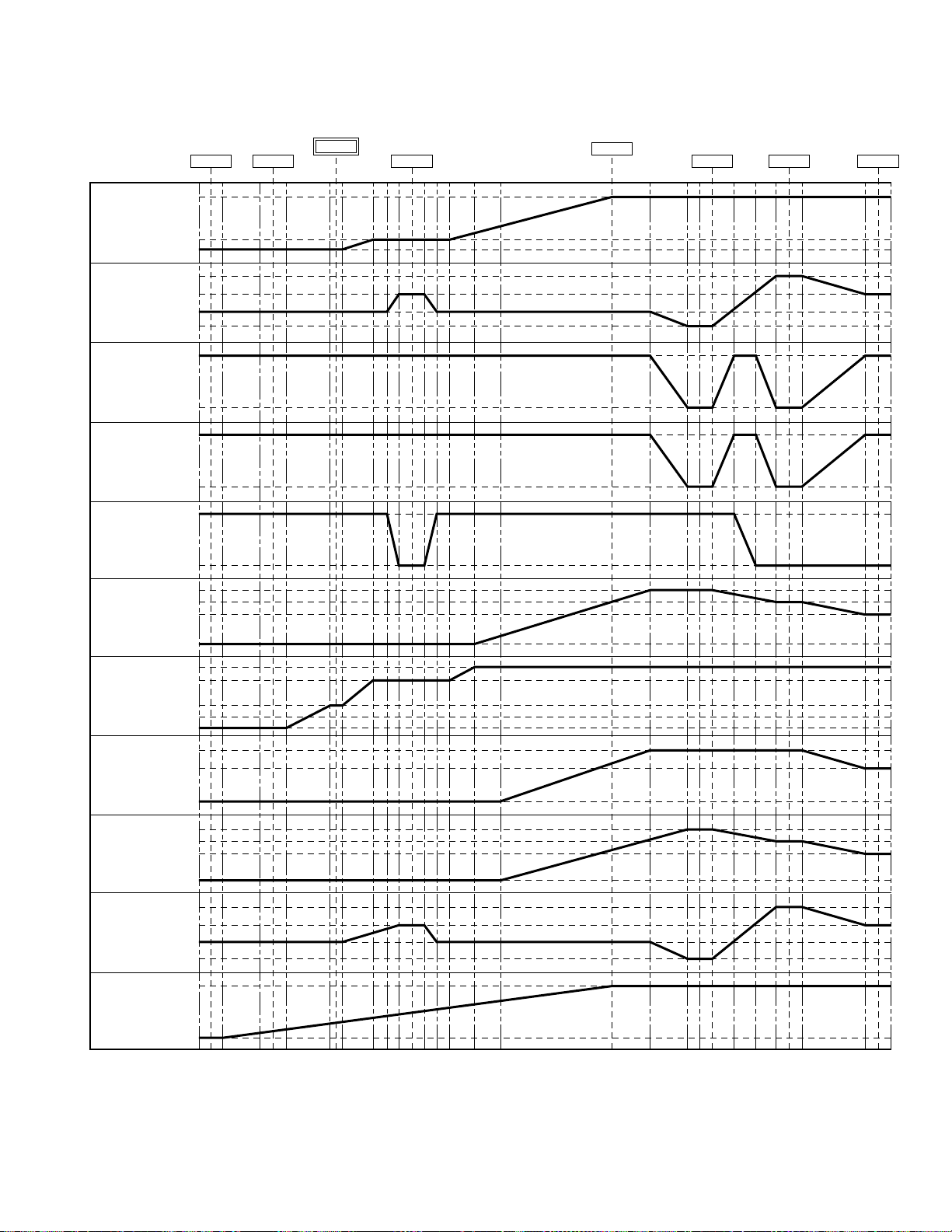
2.3 MECHANISM TIMING CHART
See following table (Table 2-3-1).
EJECT C-IN H. LOAD
ON
POLE BASE
OFF
OFF
OFF-OFF
CTL PLATE
MAIN BRAKE(S)
MAIN BRAKE(T)
SUB BRAKE
ON-OFF
ON-ON
OFF-ON
ON
OFF
ON
OFF
ON
ASSEMBLY
L-END
REV FWD STOP
ON(REV MODE)
ON(PLAY MODE)
PINCH ROLLER
EXIT GUIDE ARM
TENSHION ARM
BAND ARM PLATE
CENTERRING ARM
OFF1
HALF LOADING
ASSEMBLY
CLEANER ON
OFF1
OFF1
OFF1
TU CENTERRING
FREE
SUP CENTERRING
S. REV
C. HOUSING LOCK
OFF
OFF
ON
OFF
ON
OFF
ON
OFF
ON
OFF
Table 2-3-1
2-3
Page 31

2.4 MAINTENANCE AND INSPECTION OF MAJOR PARTS
Periodical inspection and maintenance are requisite to maintain
the initial performance and reliability of the product. Table 2-4-1
(Maintenance & Inspection List) has been compiled assuming
standard operating conditions, and the specifications in the table are greatly variable depending on the actual operating environment and conditions. Remember that, if the maintenance
and inspection are not enforced properly, the operating hours of
2.4.1 Layout of major parts
19 1 18 41 3
2
22
8
the product will not only reduce considerably but other
unfavorable influences may produce.
Rubber parts may deform or degrade after long period of storage even if they are not used in this period.
The service life of the drum is variable depending on the tape
used and operating environment.
43 45
9
5
44
15
7
14
47
2
34
35
12 2410 2513
23
6
47
46
2-4
38
37
Page 32

2.4.2 Maintenance and inspection list
1) The 6000 H maintenance consists of a replacement of the entire mechanism assembly.
2) When mounting the capstan motor on the main deck, control of the verticality is required. Therefore, when the capstan motor
reaches the end of its service life, the entire mechanism assembly should be replaced.
Part Name Ref.
Tape transport parts
1
2
Gear cover assembly
2
3
Tension arm assembly
8
4
Guide rail (S) assembly
(
5
Guide rail (T) assembly
*
6
Middle catcher assembly
3
7
Capstan shaft
q
8
Pinch roller arm assembly
5
9
Exit guide arm assembly
9
10
11
12
13
14
15
16
18
19
20
21
22
23
24
25
26
27
28
29
30
31
32
33
Drum assembly
1
Capstan motor
q
Reel drive pulley assembly
fi
R.drive gear 1
e
R.drive gear 2
r
Center gear assembly
›
Timing belt
‹
Sub-brake assembly
6
Main brake (S) assembly
@
Main brake (T) assembly
#
Reel disk assemblies
$ %
Band arm plate assembly
7
Swing arm assembly
0
Wheel gear-2
¤
Encoder gear
¢
Centering arm assembly
¶
Min cam
∞
Sub cam
•
Cleaner arm assembly
t
Cassette guide pin (Sub deck)
u
MIC contact (Sub deck)
y
Mechanism assembly (including cassette housing assembly)
FAN motor
Symbol
No.
46
M8
40
M8
22
M8
23
M8
24
M8
M8
44
M8
43
M8
50
M8
M8
33
M8
47
M8
48
M8
34
M8
11
M8
36
M8
38
M8
37
M8
39
M8
41
M8
42
M8
M8
21
M8
26
M8
M8
M8
43
M8
35
M8
35
M8
M8
43
M2
Operating Hours (DRUM Hour Meter)
500
1000
1500
2000
>
>
>
>
>
4
4
>
>
>
>
3
8
9
1
2500
3000
>
>
>
>
3500
4000
>
>
>
>
>
4500
5000
>
>
>
>
5500
6000
2.7.14
2.7.8
2.7.12
2.7.12
2.7.5
2.7.3
2.7.4
2.7.2
2.7.15
2.7.15
2.7.15
2.7.14
2.7.14
2.7.10
2.7.10
2.7.10
2.7.11
2.7.8
2.7.7
2.7.2
2.7.18
2.7.18
2.7.18
2.7.19
2.7.4
: Clean with ethanol. : Check and replace if required. : Replace. >: Oil the shaft.
After replacing a part, apply lubricant to the required points.
Table 2-4-1
2-5
Page 33

2.4.3 Cleaning
The mechanism incorporates a video head cleaner that is effective for the removal of magnetic dust, etc. However, tape lubricant adhering to the head surface produces a spacing loss, it is
recommended to polish the heads using a head cleaning tape.
When the video heads become soiled an increase in the error
rate results. Eventually, when the error rate increase is too much
to be corrected by the error correction circuit, block noise will
be observed in the picture.
1) Cleaning the video heads
Use the DVC cleaning cassette for cleaning the video heads.
Always be sure to use the cleaning cassette, Part No. MDV12CLAUX.
The video heads should be cleaned periodically. Moreover, care
should be taken about the operating environment as the tape
running time standard varies accordingly. Please refer to “Precautions for Use of Head Cleaning Tape” in the instructions.
Caution
As the DVC cleaning tape has a much higher lap-
ping effect than VHS cleaning tapes, frequent use
of the DVC cleaning tape will reduce the head service life. Do not play the DVC cleaning tape for more
than 10 seconds per run or for more than 4 times
per cleaning session.
The cleaning tape can be used effectively for up to
about 4 passes. It cannot improve the cleaning effect even if it is run for more than 4 times.
3) Cleaning the tape transport system
Moisten the tip of a cotton swab with alcohol and use it to
clean the tape transport parts. Take special care of the TU/
SUP guide roller flanges and the rear sides of the inclined
poles, as these are the parts that most frequently collect
magnetic dust.
Caution
Do not wipe the capstan shafts using alcohol. Otherwise, the oil in the bearings may be diluted by the
alcohol and become attached to the tape.
Ta ke special care.
Fig. 2-4-2 Guide Roller
2.4.4 Oiling and greasing
Table 2-4-2 shows the oil and greases used with the set.
Classification
Oil
Grease
Name
Cosmo Hydro HV100
Maltemp SH-P
Hanal
Part No.
YTU94027
KYODO-SH-P
RX-410R
2) Cleaning the upper/lower drums
Use a cleaning cloth or high-quality paper sheet to clean the
upper drum. Moisten the cloth or paper sheet with a small
amount of ethyl alcohol, apply it lightly against the upper
drum while turning it by hand.
After this operation, wipe it with a dry cloth or paper sheet
without alcohol. Be sure to play the cleaning tape to its end.
The lower drum tends to gather magnetic dust, etc. in its
lead section, and linearity cannot be achieved if this becomes
excessively dirty. The tape inlet and outlet areas are contaminated particularly easily, causing trouble such as dropout in FM signal reproduction, block noise on one side of a
monitored picture, absence of audio output or incapability of
time code readout. To clean the lead section, use a toothpick and rub lightly along the lead section. Be careful not to
scratch the video head when this is done.
High-quality paper
Apply lightly.
Core drum
Carefully clean the lead tape inlet/outlet.
Upper drum
Head tip
Toothpick
Lead
Lower drum
Table 2-4-2
1) Oiling should be performed periodically. Oil the shafts by
referring to the maintenance table.
2) After replacing a part, grease the required points. For the
parts to be greased see the exploded diagram in chapter 5,
“DISASSEMBLY DRAWINGS AND PARTS LIST”.
3) As Hanal separates over time, be sure to mix it (shake) well
before use.
4) Take care not to leave grease or oil on the tape transport
parts which come into contact with the tape or on the brake
pads.
5) Take care not to apply too much oil or grease. The standard
oiling quantity is one drop and the standard greasing quantity is the quantity with which the grease does not overflow.
2-6
Fig. 2-4-1
Page 34

2.5 PERIODICAL MAINTENANCE
Perform maintenance at the correct times in accordance with the maintenance table.
Fig. 2-5-1 shows the flow chart of periodical maintenance procedures at different operating hours.
6000-hour maintenance2000-hour maintenance
StartStart
Replaced parts
Gear cover
⁄
Tension arm assembly
8
Guide rail (SUP) assembly
(
Guide rail (TU) assembly
*
Middle catcher assembly
3
Pinch roller arm assembly
5
Exit guide arm assembly
9
Drum assembly
1
Reel drive pulley assembly
fi
R. drive gear 1
e
R. drive gear 2
r
Center gear assembly
›
Timing belt
‹
Sub-brake assembly
6
Main brake (TU) assembly
#
Reel disk assembly
$%
Band arm plate assembly
7
Swing arm assembly
0
Wheel gear-2
2
Encoder gear
¢
Centering arm assembly
¶
Main cam
∞
Sub cam
•
Cleaner arm assembly
t
Replaced parts
Mechanism assembly
including capstan motor
and cassette housing assembly
2.11 Torque adjustment
2.12 Compatibility adjustment
3.5.1 PB switching point adjustment
3.5.2 Recording current adjustment
3.5.3, 3.5.4 VCO center frequency adjustment
End
2.11 Torque adjustment
2.12 Compatibility adjustment
3.5.1 PB switching point adjustment
3.5.2 Recording current adjustment
3.5.3, 3.5.4 VCO center frequency adjustment
End
Fig. 2-5-1
2-7
Page 35

2.6
DISASSEMBLY/ASSEMBLY OF MECHANISM ASSEMBLY
2.6.1
Assembly/disassembly
The following table shows the mechanism assembly/disassembly procedures.
: Names of the disassembled/assembled parts.
1
: Items of disassembly.
2
: Parts to be removed for disassembly, such as screws, wash-
3
ers and springs, and points.
2.6.2 Screws and washers used in mechanism assembly
disassembly/assembly
Table 2-6-1 shows the symbols, designs, part numbers and colors
of the screws and washers used with the Mechanism assembly.
When disassembling or assembling the Mechanism assembly,
be sure to attach the correct screws and washers by referring
to the following table.
Symbol
S
W
P
*
1
2
3
4
Name or Point
Screw
Washer
Spring
Connector, lock (L), soldering (SD), shield, etc.
Part Name
Cassette housing assembly, ıMain deck assembly
Å
Drum assembly
1
Motor bracket (Gear cover) assembly
2
Middle catcher assembly
3
↑
1
Item No.
1
2
2
5
↑
2
Symbol
(S1)
(S2)
(S3)
(S4)
(S5)
Symbol
W1
W2
W3
2(S1), 2(L1)
3(S2)
2(S2)
3(S2)
Design
Design Part No.
Fig. 2-6-1
Points
↑
3
Part No.
QYSDSP2005Z
YQ43893
YQ43893-7
QYSPSF2006Z
LL40426-001A
YQ44246
YQ44246-3
YQ43933-2
Remark
Color
Gold
Silver
Black
Gold
Silver
Color
Red
Black
Black
2-8
Page 36

2.6.3 Mechanism assembly disassembly procedure table
No. Part Name
1
2
3
4
5
6
7
8
9
10
11
12
13
14
15
16
17
18
19
20
21
22
23
24
25
26
27
28
29
30
31
32
33
34
35
36
37
38
39
Cassette housing assembly 1 2 (S5), 2 (L1)
Å
Drum assembly 2 3 (S2)
1
Motor bracket (Gear cover) assembly 2 2 (S2)
2
Middle catcher assembly 5 3 (S2)
3
Reel cover assembly 6 (S2), 2 (L6)
4
Pinch roller arm assembly 3 (W1), (L7)
5
Sub-brake assembly 10 (P1), (W1), (L8)
6
Band arm plate assembly 8 (S3), (L9), (P2), (W2)
7
Tension arm assembly
8
Exit guide arm assembly 4 (W1)
9
Swing arm assembly 7 – Position alignment
0
Sub-deck assembly 9 5 (S2) Position alignment
!
Main brake (SUP) assembly 10 (P4), (L10)
@
Main brake (TU) assembly 10 (P5), (L11)
#
Reel disk assembly (SUP) 11 –
$
Reel disk assembly (TU) 11 –
%
Prism 7 (S2)
^
Control plate 11 2 (L12)
&
Guide rail (TU) assembly 12 4 (S2) Position alignment
*
Guide rail (SUP) assembly 12 (S2), 2 (L13) Position alignment
(
Wheel gear 2 13 –
¤
Timing belt 13 –
‹
Center gear assembly 13 –
›
Reel drive pulley assembly 14 (W1)
fi
Tension control arm assembly 15 (L15) Position alignment
·
Brake control arm assembly 15 (W1), (L16) Position alignment
‚
Charge arm assembly 15 (L17) Position alignment
¡
Encoder gear 16 – Phase alignment
¢
Main cam 16 (W1) Phase alignment
∞
Arm gear 1 assembly 16 Collar Position alignment
§
Centering arm assembly 16 – Position alignment
¶
Sub cam 17 (S2) Phase alignment
•
Arm gear 2 assembly 17 – Position alignment
ª
Clutch lock lever (C.P.D arm) assembly 17 (L19) Position alignment
º
Capstan motor – –
q
Drum base deck – 3 (S2)
w
R.drive gear 1 14 (W1)
e
R.drive gear 2 14 (W1)
r
Cleaner (Exit guide) arm assembly 4 (W1)
t
Item No.
8 (P3)
Table 2-6-2
Points Remark
Change with mechanism assembly
2-9
Page 37

4219 1 18 41 3
43 45
36
2
9
2
5
22
8
29
7
14
47
44
16
15
31
17
47
34
39
35
6
37
38
40
46
12
10
2430411 2513
23
Fig. 2-6-1
2.6.4 Mechanism disassembly/assembly procedure chart
<How to read the chart>
⋅ The following chart shows the disassembly/assembly procedures by dividing them into blocks A to I.
⋅ To remove the tension arm sub-assembly which is located in block D; start disassembly from block A. The tension arm sub-assembly
can be removed as the fourth operation after the removals of the cassette housing assembly (block A) → reel cover assembly (block
B) → band arm plate assembly (block C).
⋅ The parts enclosed in thick frames are the maintenance parts listed in the maintenance table.
⋅ For details on the disassembly/assembly, see section 2.7, “Replacement of Major Parts”.
2-10
A
B
C
D
E
F
G
H
I
BLOCK
BLOCK
BLOCK
BLOCK
BLOCK
BLOCK
BLOCK
BLOCK
BLOCK
Motor bracket
2
assembly
Assembly Procedure
Disassembly Procedure
Drum assembly
1
Guide rail
*
(TU) assembly
Guide rail (SUP)
(
assembly
pulley assembly
q
Drum base
w
deck
3
Tension arm
8
sub-assembly
Timing belt
‹
Reel drive
fi
Capstan motor
assembly
Middle catcher
assembly
Band arm
7
plate assembly
$
assembly (SUP)
Center gear
›
assembly
Reel base
Arm gear 1
§
assembly
Swing arm
0
assembly
Prism
^
Tension control
·
arm assembly
Main cam
∞
¶
arm assembly
Fig. 2-6-2
housing assembly
4
Centering
Cassette
Å
Reel cover
assembly
Main brake
@
(SUP) assembly
Sub-deck
!
assembly
Brake control
‚
arm assembly
Main brake
#
(TU) assembly
Base plate
)
assembly
Sub-brake
6
assembly
Reel base
%
assembly (TU)
Control plate
&
Clutch lock
º
lever assembly
Pinch roller
5
arm assembly
EXIT guide
9
arm assembly
Charge
¡
arm assembly
Sub cam
•
Arm gear 2
ª
assembly
Page 38

No.
Item Reference picture/drawing Procedure
2.7 REPLACEMENT OF MAJOR PARTS
⋅ Make sure that the mechanism is in the ASSEMBLY mode before proceeding to disassembly or assembly. (See section 2.1,
“Assembly Mode”.)
⋅ Screws must always be tightened using a torque screwdriver and at the specified torque.
1
Cassette housing assembly
Å
(L1)
1
(S5)
2
(S5)
<Removal>
Cassette housing assembly
1
See the 1.3.2 Cassette housing on the page 1-4.
Outer unit assembly
2
1) Align the boss
ing to the round hole
that pulls out the cassette hous-
Å
of Outer unit assembly,
ı
and then remove it.
2
B
Fig. 2-7-1
Drum assembly, 2 Motor bracket (Gear cover)
1
assembly
(S2)
4
8
(S2)
(S2)
(S2)
7
2
(L1)
A
<Attaching>
1)Reverse the removal procedure.
<Removal>
Drum assembly
1
3
1)Remove the 3 screws (S2) and take out the assembly.
5
(S2)
Motor bracket (Gear cover) assembly
2
1)Remove the 2 screws and take out the motor
bracket assembly.
2) After removing the lock of the motor bracket, the
motor can be removed by lifting the motor upward.
1
Fig. 2-7-2
<Attaching>
1) Reverse the removal procedure
NOTE
⋅ When mounting the motor, make sure that
the claw of the motor bracket is properly
locked.
If the claw is not properly locked, change the
direction for mounting the motor.
2-11
Page 39

No.
Item Reference picture/drawing Procedure
3
Pinch roller arm assembly
5
5
Fig. 2-7-3
(W1)
A
(L7)
<Removal>
1)Remove the washer (W1) and pull out the assembly.
<Attaching>
1) Fit the pinch roller arm assembly
(L7) of the charge arm assembly.
2) Attach the washer (W1).
into the boss
Å
4
Exit guide arm assembly
9
Cleaner arm assembly
t
<Removal>
1)Remove the washer (W1) and pull out the assembly.
45
(W1)
<Attaching>
1)Reverse the removal procedure.
9
Fig. 2-7-4
2-12
Page 40

No.
5
Item Reference picture/drawing Procedure
Middle catcher assembly
3
12
(S2)
Fig. 2-7-5
10
(S2)
11
(S2)
<Removal>
1)Remove the 3 screws (S2) and remove the assembly.
3
<Attaching>
1)Reverse the removal procedure.
6
Reel cover assembly
4
7
Swing arm assembly
0
(L6)
(L6)
4
10
13
(S2)
Fig. 2-7-6
<Removal>
1)Remove the screw (S2).
2)Slide the assembly toward the drum and lift the
assembly up to remove it.
NOTE
⋅ After having removed the reel cover, take care
because the parts located below the reel
cover tend to slip out easily.
<Attaching>
1)Insert the reel cover into (L6) and attach by reversing the removal procedure.
<Removal>
1) Pull the assembly upward.
Fig. 2-7-7
<Attaching>
1) Reverse the removal procedure.
2-13
Page 41

No.
8
Item Reference picture/drawing Procedure
Band arm plate assembly, 8 Tension arm assembly <Removal>
7
14
(S3)
(W2)
7
(P2)
1)Remove the washer (W2).
2)Remove the screw (S3).
3)Remove the spring (P2).
4)Remove the band arm plate assembly and tension
arm assembly.
(P3)
(L9)
Fig. 2-7-8(a)
Attaching the spring
Step 1
8
NOTE
Be careful not to lose the spring (P3).
<Attaching>
1) Attach the spring (P3) to the tension arm assem-
bly. Engage the longer end of spring to hook
and the shorter end to hook b as shown in Fig. 27-8(b).
2) Attach the tension arm sub-assembly.
3) Attach the band arm plate assembly.
4) Clamp with the screw (S3) and washer (W2).
5) Attach the spring (P2) to (L9).
NOTE
After attaching, ensure that the band arm assembly can rotate in the direction of the arrow as
shown in Fig. 2-7-8(c).
Attach so that the section
side of the tension arm assembly
comes on the outer
Å
.
8
a
2-14
Hook (Longer end)
a
Step 2
Hook (Shorter end)
b
Step 3
Fig. 2-7-8(b)
The spring (P3) should be attached only to the tension
arm assembly
not contact the band arm
plate assembly
. It should
8
.
7
Å
Fig. 2-7-8(c)
6) After attaching, adjust the tension.
Page 42

No.
Item Reference picture/drawing Procedure
8 <Tension arm assembly position adjustment> 1)Without loading a tape, set the mechanism mode
to PLAY mode.
To switch the mode, rotate wheel gear 2 while the
motor bracket assembly is disengaged (see 2.2,
“Mechanism Modes”).
2)Rotate the tension arm slightly clockwise to eliminate production of rattle with the band arm plate.
3)Ensure that the notch on the tension arm is located
within area A. (See Fig. 2-7-8(e).)
A
4)If the tension arm is not located in area A, loosen
screw B (black) lightly and fine-adjust the position
of the band arm plate assembly. Turn the screw
Notch on tension arm
counterclockwise to move the tension arm extremity toward the right or clockwise to move it toward
the left.
5)After the adjustment, clamp the band holder by
tightening screw B (black) (with a securing torque
of 5.88 Nm, or 0.6 kgf-cm). Then adjust the tension arm position again.
Notch on tension arm
Tension arm
Band arm plate
B (Black)
Counterclockwise
direction
Fig. 2-7-8(d)
Screw
Turn the tension arm
in the clockwise direction.
Joint between the tension arm
and band arm plate
(must not rattle here.)
Clockwise
direction
Band holder
A
0.5
0.5
OK (Lower limit)
No Good
OK (Center)
No Good
OK (Upper limit)
Fig. 2-7-8(e)
2-15
Page 43

No.
9
Item Reference picture/drawing Procedure
Sub-deck assembly <Removal>
!
15
(S2)
35
(S2)
18
(S2)
17
(S2)
11
The boss should
fit into the hole.
Phase alignment
Control plate
(
L11
16
(S2)
)
1)Remove the 5 screws (S2) and pull out the assembly.
<Attaching>
1)While sliding the control plate toward the left, attach the sub-deck assembly.
NOTE
⋅ Attach by aligning the phase holes of the
main deck assembly and control plate.
Fig. 2-7-9
10@ Main brake (SUP) assembly, # Main brake (TU) assembly,
Sub-brake assembly
6
12
(P4)
13
(
)
L10
(P5)
(W1)
(
L11
)
(L8)
11
2)Clamp with 5 screws (S2).
<Removal>
Main brake (SUP) (TU) assembly
1)Remove the spring by disengaging its ends from
the hooks (L10) and (L11).
Sub-brake assembly
1)Remove the washer (W1).
2)Remove the spring by disengaging it from the hook
(L8).
<Attaching>
1)Reverse the removal procedure.
2-16
6
(P1)
Fig. 2-7-10
Page 44

No.
Item Reference picture/drawing Procedure
11
Reel disk (SUP) assembly, % Reel disk (TU) assembly,
$
Control plate, ^ Prism
&
14
15
17
(
)
L12
(
)
L12
Fig. 2-7-11
11
16
<Removal>
1)Pull up each assembly to remove it. The control
plate can be removed by sliding it toward the left
as shown by the arrow.
2)Remove the screw (S2) to remove the prism.
<Attaching>
1)Reverse the removal procedure.
12
Guide rail (TU) assembly, ( Guide rail (SUP) assembly
*
(
)
L13
24
(S2)
19
21
(S2)
20
(S2)
22
(S2)
23
(S2)
18
<Removal>
Guide rail (TU) assembly:
1)Remove the 4 screws (S2) and remove the assembly.
Guide rail (SUP) assembly:
1)Remove the screw (S2) and remove the assembly.
<Attaching>
1)Return the guide pole fully to the unloading position, and attach the assemblies by reversing the
removal procedures. When attaching, place the
alignment markings of the two gears so that they
face each other. (See Fig. 2-7-12(b).)
19
18
Fig. 2-7-12(a)
Fig. 2-7-12(b)
2-17
Page 45

No.
Item Reference picture/drawing Procedure
13¤ Wheel gear 2, ‹ Timing belt, › Center gear assembly
23
24
22
Fig. 2-7-13
<Removal>
1)Each parts can be removed by simply pulling them
out.
<Attaching>
1)Reverse the removal procedure.
14
Reel drive pulley assembly, e R. drive gear 1, r R. drive gear 2
fi
(W1)
25
43
(W1)
44
(W1)
Fig. 2-7-14
<Removal>
1)Remove the washer (W1) and take out the assembly.
<Attaching>
1) Reverse the removal procedure.
2-18
Page 46

No.
Item Reference picture/drawing Procedure
15· Tension control arm assembly, ‚ Brake control arm assembly,
Charge arm assembly
¡
(
)
L16
(W1)
30
(
)
L17
(
L15
)
31
29
<Removal>
1)The brake control assembly can be removed after
removing the washer (W1).
<Attaching>
1)Align the phases of the main cam and sub cam ,
then attach by reversing the removal procedure.
Refer to Fig. 2-7-15(b) and Fig. 2-7-15(c).
Fig. 2-7-15(a)
34
30
Bosses
29
(Phase alignment)
35
Align the phase of the main cam ∞ then attach by fitting the
bosses in the cam groove.
Fig. 2-7-15(b)
Attaching Tension Control Arm Assembly
and Brake Control Arm Assembly
·
‚
31
•
39
, then
38
Phase
alignment
Bosses
(Phase alignment)
Phase alignment
Boss (Phase alignment)
Align the phase of the sub cam
attach by fitting the boss into the cam groove.
Fig. 2-7-15(c) Attaching the Charge Arm
Assembly
¡
2-19
Page 47

No.
Item Reference picture/drawing Procedure
16¢ Encoder gear, ∞ Main cam , § Arm gear 1 assembly,
Centering arm assembly
¶
34
37
(W1)
Collar
36
Fig. 2-7-16(a)
35
<Removal>
1)The main cam can be removed by removing the
washer (W1). As the cam gear is engaged at the
rear of the main deck assembly while the phase is
aligned, deviate the phase in the direction of the
arrow before removal. (See Fig. 2-7-16(b).)
37
Phase alignment
Fig. 2-7-16(b) Removing the Centering Arm
Assembly
¶
Phase alignment
Marking
Å
34
35
Phase alignment
Align the phase of the main cam ∞, then attach by aligning the redcolored markings
(on 2 gear teeth) inside Q.
Å
<Attaching>
1)Align the phase by referring to Figs. 2-7-16(c) and
2-7-16(d), then attach the ass’ies reverse the removal procedure.
35
Phase
alignment
36
Phase
alignment
37
Phase alignment
Align the phases of the arm gear 1 assembly
and centering arm assembly ¶, then align those
of the arm gear 1 assembly
arm assembly
bosses into the cam groove below, and fit the
slit washers.
, attach the gear by fitting the
¶
and centering
§
§
2-20
Fig. 2-7-16(c) Attaching the Rotary Encoder Assembly
¢
Fig. 2-7-16(d) Attaching the Main Cam
∞
Page 48

No.
Item Reference picture/drawing Procedure
17
Sub cam ª Arm gear 2 assembly, º Clutch lock lever assembly
•
31
(S2)
38
40
(
L19
)
39
<Removal>
1)Remove the screw (S2) and take out the sub cam .
As L19 is engaged at the rear of the main deck
assembly while the phase is aligned, deviate the
phase in the direction of the arrow before removal.
20. This checking should be done after completing the
switching point adjustment.
Phase alignment
40
Fig. 2-7-17(b) Removing the Clutch Lock Lever
Assembly
º
Fig. 2-7-17(a)
<Attaching>
1)Align the phase correctly by referring to Fig. 2-717(c), then attach by reversing the removal procedure.
39
38
Phase
alignment
Phase
alignment
40
Phase
alignment
Align the phases of the arm gear 2 assembly
and clutch lock lever assembly º, attach them by
fitting the boss into the cam groove below, and
clamp with the screw.
Fig. 2-7-17(c) Attaching the Sub Cam
ª
•
2-21
Page 49

2.8 CONFIRMATION AND ADJUSTMENT OF MECHANISM PHASES
See Fig. 2-8-1.
Encorder gear
34
assembly
See section 2.7.16
Arm gear 1 assembly
36
See section 2.7.16
Arm gear 2 assembly
39
See section 2.7.17
Sub cam
38
See section 2.7.17
Main cam
35
See section 2.7.16
Centering arm assembly
37
See section 2.7.16
Fig. 2-8-1
Clutch lock lever assembly
40
See section 2.7.17
2-22
Page 50

2.9 DISASSEMBLY PROCEDURE LIST
45
(W1)
7
8
14
15
(W2)
(P3)
14(S3)
15
(S2)
16
(S2)
12
17
29
13
11
6
2
38
42
3
19
1
18
10
4
23
(S2)
22
(S2)
10
(S2)
11
(S2)
3
(S2)
4
(S2)
24
(S2)
5
(S2)
12
(S2)
34
(S2)
32
(S2)
33
(S2)
31(S2)
20
(S2)
18
(S2)
21
(S2)
17
(S2)
7(S2)
8(S2)
(W1)
16
19
(S2)
B
(P7)
ADJ.
NUT
(W1)
(W1)
(W1)
(W1)
(W1)
13
(S2)
Collar
35
30
22
34
23
24
36
40
39
5
31
43
9
41
37
(W1)
(W1)
25
44
Note) For the grease and oil application points,
see section 5.6, ''MECHANISM ASSEMBLY PARTS LIST
Fig. 2-9-1
M6
''
2-23
Page 51

2.10 MECHANISM DISASSEMBLY/ASSEMBLY SHEET
Screw Management
Drawing No.
No.
Table
2S53S24S25
S5
S2
7S28
S2
1
Application
10
S2
11S212
S2
13
S2
!Å12347
15S216S217S218S235
14
S3
S2
Ref. No.
Cassette housing assembly
Å
No.1 No.2 No.5 No.9
1
(S5)
No.8
Drum assembly
1
4
(S2)
2
(S5)
S2
×
3
Motor bracket assembly
2
8
(S2)
A
B
×
4
S2
Middle catcher assembly
3
12
(S2)
3
(S2)
10
(S2)
5
(S2)
7
(S2)
11
(S2)
Reel cover assembly
4
(S2)
S2,L6
×
2
Pinch roller arm assembly
5
(W1)
W1,7
Sub-brake assembly
6
(W1)
13
(P1)
S37×2
Control plate
&
×
2
L12
Center gear
›
assembly
Main cam
∞
Reel drive
fi
pulley assembly
(W1)
W1
(W1)
*
S2
Arm gear 1 assembly
§
Collar
Collar
×
3
S2
Guide rail (TU) assembly
20
(S2)
21
(S2)
×
4
Centering arm assembly
¶
22
(S2)
23
(S2)
Tension control arm
·
assembly
(
L15
P1,W1,L8
Guide rail (SUP) assembly
(
(
)
L13
S2,L13×2
)
Sub cam
•
24
(S2)
Brake control
‚
arm
assembly
(
) (W1)
L16
W1,L16
31
(S2)
2-24
W1 S2
Collar
Page 52

Screw Management
^*( w
•
19 20 21 22 23 24 31 32 33 34
S2 S2 S2 S2 S2 S2
No.11 No.17
Band arm plate assembly
7
(P2)
S3,P2,L9,W2
Tension arm assembly
8
(P3)
P3
Exit guide arm assembly
9
Cleaner arm assembly
t
No.12
14
(S3)
(W2)
(W1)
S2 S2 S2 S2
Sub-deck assembly
!
(S2)
S2×5
Swing arm
0
assembly
16
−
R. drive
e
15
(S2)
(S2)
gear 1
35
18
(S2)
R. drive
r
gear 2
(W1) (W1)
17
(S2)
The slit washers cannot
be reused once they
have been removed.
Main brake
@
(SUP) assembly
(P4)
P4,L10 P5,L11
Reel base
$
assembly (SUP)
Prism
^
Main brake
#
(TU) assembly
(P5)
Reel base
%
assembly (TU)
19
(S2)
W1
Charge arm assembly
¡
(
)
L17
L17
Arm gear 2 assembly
ª
(W1)
Clutch lock lever assembly
º
(C.P.D arm assembly)
Wheel gear
¤
Capstan motor
q
ADJ NUT
S2
Timing belt
‹
Encorder gear
¢
Drum base deck
w
33
(S2)
32
(S2)
34
(S2)
L19 S2×3ADJ NUT,P7
(P7)
2-25
Page 53

No. Item instruments & Mode
Measuring
Input signals
2.11 TORQUE ADJUSTMENTS
1 SUP backup
torque
• Cassette torque
meter
Play (1) Insert the cassette torque meter and enter play
adjustment
Tension arm
Band arm plate
Screw (Black)
Measuring point (*)
Adjustment parts (-)
Adjustment level (+)
* Supply side indica
tion of cassette
torque meter
+1.47
+ 3.9 x 10
-0.39
(4.0 gf·cm)
+1.5
-0.4
-4
N·m
Adjustment procedure
mode.
(2) The supply backup torque should be as speci-
fied. (If it fluctuates, read the center value.)
(3) If it is out of specification, eject the tape, re-
move the cassette housing, loosen the screw
(black) slightly and fine-adjust the band holder.
Slightly turn the band holder as follows.
⋅ To increase torque: Counterclockwise
⋅ To decrease torque: Clockwise.
NOTE
The screw securing torque should be 0.0588
N-m (0.6 kgf⋅cm).
4) Check the supply backup torque again and repeat the above steps until it becomes as specified.
2 Take-up wind
torque
adjustment
Counterclockwise
Cassette torque
meter
YTU94150A
Clockwise
PLAY,
Adjustment
menu No. 110
Band
holder
* Take-up side reading
of cassette torque
meter
+4.90
+ 4.9
x 10-4 N·m
-1.96
+5.0
(5.0 gf·cm)
- 2.0
1) Select adjustment menu [119. FWD TORQUE].
(For the adjustment menu, see 3.3, “Adjustment menu”.)
2) Insert the torque cassette meter YTU94150A
and press the [PLAY] button.
3) Adjust the TU wind torque so that it is within
the specified range.
⋅ Press JOG dial to enter the adjustment mode.
⋅ To increase the torque → Rotate JOG dial to
the clockwise.
⋅ To decrease the torque → Rotate JOG dial to
the counter-clockwise.
4) After adjustment, press JOG dial to store the
adjustment data.
2-26
Page 54

2.12 COMPATIBILITY ADJUSTMENT
NG
NG
NG
NG
NG
NG
OK
OK
OK
OK
OK
OK
Start
Connect the connector board.
Set the RF envelope adjusted waveform flat.
Is the envelope flat?
Is the envelope
restored within 1 second after mode
transition from Eject to Play?
Eject the cassette tape and start
playback. Is the envelope still flat?
Is the envelope restored
within 1 second after mode transitions
from SEARCH FWD to PLAY and from
SEARCH REV to PLAY?
Electrical
adjustments
Tension band or
main brake
assembly defect.
Tension error.
Check the envelope during
FF and REW, and confirm that the specified
waveforms are output in both modes.
Transport system
part defect.
Enter modes PLAY → SEARCH REV →
SEARCH FWD → PLAY in this sequence,
and ensure that tape is not damaged
by wrinkles.
2.12.1 Compatibility adjustment flow chart
Fig. 2-12-1 shows the flow chart of compatibility adjustment.
Fig. 2-12-1
2-27
Page 55

13.6
6
TU guide roller
Upper restriction
7
MID guide roller
No restriction
8
MID guide roller
No restriction
9
Capstan shaft
No restriction
!
Exit guide pole
No restriction
Reference plane (Top of main deck)
Tape sensor
2.12.2 Tape transport restriction
1
± 0.02
19.25
(10.35)
13.6
Reference plane (Top of main deck)
Tape sensor
1
Entrance guide pole
No restriction
2
Tension pole
No restriction
3
SP guide roller
Upper restriction
4
SUP slant pole
No restriction
The unit uses only the SUP guide roller and TU guide roller to
restrict the tape transport. The tape is free (no restriction) from
other parts.
2
Entrance guide pole
3
Tension pole
SP guide roller
SUP slant pole
4
5
Drum
TU guide roller
6
Pinch roller
0
Fig. 2-12-2
MID guide roller
7
TU slant pole
8
Capstan shaft
9
Exit guide pole
!
2-28
Fig. 2-12-3 Tape Restriction on Supply Side
Fig. 2-12-4 Tape Restriction on Take-up Side
Page 56

No. Item instruments & Mode
Measuring
Input signals
2.12.3 Compatibility adjustment
1 Preparation
Measuring point (*)
Adjustment parts (-)
Adjustment level (+)
Connector board
Adjustment procedure
(1) Mount a connector board to the CN23 on the
A/L/S board by inserting it in the slot that is
provided to accommodate it. This may be
achieved without removing the R. side cover.
(See Fig. 2-12-6.)
NOTE
⋅ Make sure the component surface of the
connector board is upside.
NOTE
⋅ Be sure to clean the tape transport parts
and play a cleaning tape before proceeding to the compatibility adjustment.
2 RF envelope
adjustment
Fig. 2-12-5 How to mount a connector board
• Oscilloscope,
alignment tape
MC-1(NTSC)
MC-2(PAL)
Color bar portion
Play
* TP9 ENV OUT
[connector board]
* TP5 HID [connector
board]
- Supply guide roller
- Take-up guide roller
+ Make the wave-
forms flat. The drop
level should be less
than 3 dB with both
SUP and TU levels.
+ Flatness variation
should be less than
2 dB.
(1) Play alignment tape color bar portion.
(2) Observe the measuring points and adjust the
supply guide roller and take-up guide roller so
that the RF waveform is flat.
(3) Set the mode to EJECT, then set to the PLAY
mode and ensure that the RF waveform is flat.
Error on
supply side
Error on
take-up side
Fig. 2-12-6
2-29
Page 57

No. Item instruments & Mode
Measuring
Input signals
Measuring point (*)
Adjustment parts (-)
Adjustment level (+)
Adjustment procedure
3Waveform
rise check
4 Damage
check
• Oscilloscope,
alignment tape
MC-1(NTSC)
MC-2(PAL)
Color bar portion
• Self-recorded/
played tape
60ME
Eject →Play
Search FWD
→Play
Search REV
→ Play
Play
↓
Search REV
↓
Search FWD
↓
Play
* TP9 ENV OUT
[Rewrite board]
* TP5 HID
[Rewrite board]
+The envelope
waveform should be
restored within 1
sec.
* TP9 ENV OUT
[Rewrite board]
* TP5 HID
[Rewrite board]
+The tape should not
be damaged by
wrinkle.
(1) Switch the mode from Eject → Play and en-
sure that the envelope waveform is restored
in less than 1 sec.
(2) Switch the mode from Search FWD → Play
and from Search REV → Play, and ensure that
the envelope is restored in less than 1 sec. in
both cases.
(3) If the waveform does not restore in the speci-
fied period, fine-adjust the supply/take-up
guide rollers as far as the envelope waveform
specification is met, then restart checking from
the above procedure 1 again.
(1) Transport the self-recorded/played tape from
the beginning by changing modes in order of
Play → Search REV → Search FWD → Play,
and ensure that wrinkles due to strong restriction by the guide rollers and guide pole are not
produced on tape.
(2) Perform the same check at the section near
the end of tape.
(3) Make sure that no tape damage occurs when
a tape is being loaded, unloaded or ejected.
5 Envelope
check during
FF/REW
ENV OUT
HID
• Oscilloscope,
alignment tape
MC-1(NTSC)
MC-2(PAL)
Color bar portion
FF
REW
* TP9 ENV OUT
[Rewrite board]
* TP5 HID
[Rewrite board]
+
> 55µsec.
Å
+ı T/3
ı
t
Å
T
MAX
HIGH
LOW
(1) Insert the alignment tape and enter Stop mode.
(2) Enter FF mode.
(3) Ensure that the envelope output is present at
55 µs before the HID switching timing.
(4) Check the take-up side of the envelope to see
that the MAX output duration is more than 1/3
the HID duration.
This checking should be done after completing the switching point adjustment.
(5) Enter REW mode and check the same items
as (3) and (4) above.
(6) If the envelope is out of specification, check
the tension band and main brake assembly and
replace as required. Confirm the playback
switching point.
2-30
Fig. 2-12-7
Page 58

SECTION 3
ELECTRICAL ADJUSTMENTS
3.1 FUNCTIONS REQUIRED FOR ADJUSTMENTS, SETUP
3.1.1 General instruments necessary for adjustment
Instrument Condition
Oscilloscope
Vectorscope
Audio tester
3.1.2 Special implements required for adjustment
123
Waveform monitor (WFM)
Camera and lens
Calibrated instrument with a measuring
bandwidth of 100 MHz or more.
Calibrated instrument
Calibrated instrument
Gray scale chart
(Part No.:GS2L)
Monitor TV
Instrument Condition
Frequency counter
Monitor TV
Instrument calibrated for 8 digits or more.
Stability of 0.1 ppm or 1x10
required at 0 to 40°C.
Color video monitor with a 75Ø video input.
Accessory (Model name : KA-551U)
645
Alignment tape
Tripod base
MC-1 : NTSC
MC-2 : PAL
-7
or better is
7
CK453800C
REWRITE board
Fig. 3-1-1 Special implements required for adjustment
3-1
Page 59

3.2 STANDARD SETUP
Color video monitor
Vectorscope
Test pattern
Adjustment items
For Camera-1 adjustment
No. Item name
COUNTRY
0
VIDEO MODE CHANGE
1
27MHz CAM
2
SENC SDRAM
3
FPGA4 VD
5
FPGA4 SDRAM
6
Y LEVEL[COMPOSITE]
10
C LEVEL
11
Y LEVEL[COMPONENT]
12
B-Y LEVEL
13
R-Y LEVEL
14
FPGA BLACK[B]
20
FPGA BLACK[R]
21
MASTER BLACK
22
BLACK OFFSET[G]
23
BLACK OFFSET[B]
24
BLACK OFFSET[R]
25
WHITE OFFSET[G]
37
WHITE OFFSET[B]
38
WHITE OFFSET[R]
39
IN GAIN[G]
40
IN GAIN[B]
41
IN GAIN[R]
42
FLARE[B]
43
FLARE[R]
44
MASTER FLARE
45
75 Ø resistor for
termination
3200 K illumination
Waveform monitor (WFM)
Filter 1 (3200 K)
2 m or more
Adjustment value
U_E, I_EC
NTSC, PAL
NTSC & PAL
NTSC & PAL
0 to 255
-
0 to 7
0 to 15
NTSC & PAL
NTSC & PAL
NTSC & PAL
0 to 255
0 to 255
NTSC & PAL
0 to 255
0 to 255
0 to 255
0 to 40
0 to 40
0 to 40
0 to 63
0 to 63
0 to 63
100 to 143
100 to 143
100 to 143
-
NTSC & PAL
NTSC & PAL
NTSC & PAL
NTSC & PAL
NTSC & PAL
NTSC & PAL
NTSC & PAL
-
-
0 to 40
0 to 40
0 to 20
Remarks
NTSC
NTSC
NTSC
NTSC
NTSC
NTSC
NTSC
NTSC
NTSC
NTSC
NTSC
NTSC
NTSC
75 Ø resistor for
termination
Composite cable
GY-HD100
Component cable
AC adapter
(7.2 g 9.0 V DC/3A INPUT)
No. Item name
CORING[G]L
46
CORING[G]R
47
CORING[B]L
48
CORING[B]R
49
CORING[R]L
50
CORING[R]R
51
BLACK SHADING[G]L
52
BLACK SHADING[G]R
53
BLACK SHADING[B]L
54
BLACK SHADING[B]R
55
BLACK SHADING[R]L
56
BLACK SHADING[R]R
57
For AUDIO adjustmnt
No. Item name
6061AUDIO LEVEL[CH1]
AUDIO LEVEL[CH2]
For LCD & VF adjustment
No. Item name
SUB-BRIGHT[B]
70
SUB-BRIGHT[R]
71
CONTRAST
72
SUB-CONTRAST[B]
73
SUB-CONTRAST[R]
74
GAMMA-1
75
Oscilloscope
IEEE 1394
HDV
DV
LINE OUTPUT
DC INPUT
Adjustment value
Adjustment value
Adjustment value
VIDEO/Y
B
P
R
P
IEEE1394
0 to 63
0 to 63
0 to 63
0 to 63
0 to 63
0 to 63
0 to 80
0 to 80
0 to 80
0 to 80
0 to 80
0 to 80
-
-
-
-
100 to 160
10 to 120
10 to 120
0 to 80
Remarks
NTSC & PAL
NTSC & PAL
NTSC & PAL
NTSC & PAL
NTSC & PAL
NTSC & PAL
NTSC & PAL
NTSC & PAL
NTSC & PAL
NTSC & PAL
NTSC & PAL
NTSC & PAL
Remarks
NTSC
NTSC
Remarks
NTSC
NTSC
NTSC
NTSC
NTSC
NTSC
3-2
Page 60

For LCD & VF adjustment
For LCD & VF adjustment
No. Item name
GAMMA-2
76
PSIG BRIGHT
77
COMMON DC
78
HUE
79
VCO FINE
80
BLACK LIMITER
81
VCO COARSE
82
H-POSITION
83
RESOLUTION
84
VF SUB-BRIGHT[B]
85
VF SUB-BRIGHT[R]
86
VF CONTRAST
87
VF SUB-CONTRAST[B]
88
VF SUB-CONTRAST[R]
89
VF GAMMA-1
90
VF GAMMA-2
91
VF COM LEVEL
92
VF COMMON DC
93
VF HUE
94
VF VCOL
95
VF VCOH
96
VF H POSITION
97
VF V POSITION
98
VF RESOLUTION
99
For DVC unit adjustment
No. Item name
PB SW POINT
100
ME REC CURRENT
101
ME SP VCO
102
FS PLL 48kHz
103
FS PLL 44.1kHz
104
FS PLL 32kHz
105
27MHz VCO
106
ATF GAIN
107
AGC GAIN
108
BGNEND SENS
109
FWD TORQUE
110
For CAMERA-2 adjustmnt
No. Item name
AFE ALL RESET
200
H1 START[G]L
201
H1 STOP[G]L
202
H1 START[G]R
203
H1 STOP[G]R
204
RESET START[G]L
205
RESET STOP[G]L
206
Adjustment value
0 to 80
40 to 120
27 to 107
35 to 95
0 to 255
0 to 63
1 to 7
2 to 31
0 to 5
27 to 107
27 to 107
100 to160
10 to 120
10 to 120
0 to 80
0 to 80
0 to 255
27 to 107
35 to 95
0 to 255
0, 1
0 to 79
0 to 31
0 to 5
Adjustment value
00000000 to FFFFFFFF
0 to 255
0000H to FFFFH
0 to 255
0 to 255
0 to 255
0 to 255
0 to 255
0 to 255
0 to 255
0 to 255
Adjustment value
CANCEL, EXECUTE
0 to 63
0 to 63
0 to 63
0 to 8
34 to 36
0 to 63
Remarks
NTSC
NTSC
NTSC & PAL
NTSC
NTSC & PAL
NTSC
NTSC & PAL
NTSC & PAL
NTSC & PAL
NTSC
NTSC
NTSC
NTSC
NTSC
NTSC
NTSC
NTSC
NTSC & PAL
NTSC
NTSC & PAL
NTSC & PAL
NTSC & PAL
NTSC & PAL
NTSC & PAL
Remarks
NTSC
NTSC
NTSC
NTSC
NTSC
NTSC
NTSC
NTSC
NTSC
NTSC
NTSC
Remarks
NTSC & PAL
NTSC & PAL
NTSC & PAL
NTSC & PAL
NTSC & PAL
NTSC & PAL
NTSC & PAL
No. Item name
SHP PHASE[G]L
207
SHD PHASE[G]L
208
AD OUT PHASE[G]L
209
RESET START[G]R
210
RESET STOP[G]R
211
SHP PHASE[G]R
212
SHD PHASE[G]R
213
AD OUT PHASE[G]R
214
H1 START[B]L
221
H1 STOP[B]L
222
H1 START[B]R
223
H1 STOP[B]R
224
RESET START[B]L
225
RESET STOP[B]L
226
SHP PHASE[B]L
227
SHD PHASE[B]L
228
AD OUT PHASE[B]L
229
RESET START[B]R
230
RESET STOP[B]R
231
SHP PHASE[B]R
232
SHD PHASE[B]R
233
AD OUT PHASE[B]R
234
H1 START[R]L
241
H1 STOP[R]L
242
H1 START[R]R
243
H1 STOP[R]R
244
RESET START[R]L
245
RESET STOP[R]L
246
SHP PHASE[R]L
247
SHD PHASE[R]L
248
AD OUT PHASE[R]L
249
RESET START[R]R
250
RESET STOP[R]R
251
SHP PHASE[R]R
252
SHD PHASE[R]R
253
AD OUT PHASE[R]R
254
CLAMP ALL REST
300
CLAMP LEVEL[G]L
301
CLAMP LEVEL[G]R
302
CLAMP LEVEL[B]L
303
CLAMP LEVEL[B]R
304
CLAMP LEVEL[R]L
305
CLAMP LEVEL[R]R
306
Adjustment value
0 to 63
0 to 63
0 to 16
34 to 36
0 to 63
0 to 63
0 to 63
0 to 63
0 to 63
0 to 63
0 to 63
0 to 8
34 to 36
0 to 63
0 to 63
0 to 63
0 to 63
34 to 36
0 to 63
0 to 63
0 to 63
0 to 63
0 to 63
0 to 63
0 to 63
0 to 8
34 to 36
0 to 63
0 to 63
0 to 63
0 to 16
34 to 36
0 to 63
0 to 63
0 to 63
0 to 63
CANCEL, EXECUTE
0 to 63
0 to 63
0 to 63
0 to 63
0 to 63
0 to 63
NTSC & PAL
NTSC & PAL
NTSC & PAL
NTSC & PAL
NTSC & PAL
NTSC & PAL
NTSC & PAL
NTSC & PAL
NTSC & PAL
NTSC & PAL
NTSC & PAL
NTSC & PAL
NTSC & PAL
NTSC & PAL
NTSC & PAL
NTSC & PAL
NTSC & PAL
NTSC & PAL
NTSC & PAL
NTSC & PAL
NTSC & PAL
NTSC & PAL
NTSC & PAL
NTSC & PAL
NTSC & PAL
NTSC & PAL
NTSC & PAL
NTSC & PAL
NTSC & PAL
NTSC & PAL
NTSC & PAL
NTSC & PAL
NTSC & PAL
NTSC & PAL
NTSC & PAL
NTSC & PAL
NTSC & PAL
NTSC & PAL
NTSC & PAL
NTSC & PAL
NTSC & PAL
NTSC & PAL
NTSC & PAL
Remarks
3-3
Page 61

3.3 ADJUSTMENT MENU
3.3.1 Switches and Functions Used in Adjustments
Most of the adjustment items employ microcomputer-controlled adjustments using electric potentiometers. The adjustment data is
stored in EEPROM.
The switches used in the adjustments and their functions are as follows.
• MENU (STATUS) button : Press to start or exit from the adjustment menu.
• USER 1 , USER 2 : Press to select the adjustment item.
• JOG (SHUTTER) dial (rotate) : Rotate to adjust the selected item.
• JOG (SHUTTER) dial button (push in ) : Press to start an adjustment and store the adjustment value in memory.
3.3.2 Procedure
(1) Turn the power ON, while holding the USER 1 and USER 2 buttons
(2) When the power is ON, press the MENU button to display the ADJUST MENU.
(3) Push the JOG dial button so that “*” blinks, and rotate the JOG dial to the specified value while observing the designated TP and
measuring instrument. (In this mode, JOG dial rotate while holding the MENU button, then parameter value change quickly.)
(4) After completing the adjustment, push the JOG dial button to delete the “*” and store the adjustment value in memory.
(If do not push the JOG dial button, adjustment value will not stored.)
(5) Press the USER 1 and USER 2 button to select the next item to adjust.
(6) Adjust for each item to do same procedure as above (3)(4).
(7) After completing all adjustments, press the MENU button to exit the ADJUST MENU.
(8) To return to normal operation mode, turn the power OFF and ON again.(If did not re-start camera power, camera will be still in
ADJUST MODE, so if press the MENU button then ADJUST MENU indicate on the screen and will not indicate normal menu
screen.)
AD J US T [NTSC]
4. INGAIN(B)
*
VR DATA : 1 5 5
651:TUOLTC
502:ATADTES
:
XXXXXXXXX.FER
On-screen adjustment menu
3.3.3 Adjustment mode
When setting to adjustment mode with the MENU setting status below, an adjustment mode that outputs PAL signal will be set.
• FRAME RATE : 50/25
• REC : DV-50I
:BG:R
Usually not displayed. Starts blinking
when the SHUTTER (JOG) dial is pushed.
Potentiometer value
D/A output value
Adjustment value currently set
The value changes when
the potentiometer value is
stored in memory.
Displayed as the adjustment menu items.
3-4
Page 62

No. Item
instruments &
Input signals
3.4 CAMERA ADJUSTMENTS
3.4.1 Camera adjustments
Measuring
Mode
Measuring point
Adjustment parts
Adjustment level
(*)
(-)
(+)
Adjustment procedure
FH
1
adjustment
ENCODER
2
adjustment
(COMPOSITE)
BURST
LEVEL
ENCODER
3
adjustment
(COMPONENT)
Y
B-Y
0.7
Vp-p
Frequency
counter
Oscilloscope
H-rate
Oscilloscope
ADJUST MENU
ADJUST MENU
VIDEO
LEVEL
ADJUST MENU
1.0
Vp-p
* TP[FH] Rewrite
board
- JOG dial
+ 27,000,000 ± 30Hz
(1) Press the USER 1/2 button to select ADJUST
MENU No.2 ”27MHz CAM”.(Color bar signal
will be output automatically)
(2) Push the JOG dial button so that “*” blinks,
and then rotate the JOG dial to adjust to the
specified value.
(3) Press the JOG dial to store the adjustment
data.
* VIDEO OUT
- JOG dial
+ VIDEO level
1.000Vp-p
(1) Press the USER 1/2 button to select ADJUST
MENU No.10 ”Y LEVEL (COMPOSITE)” .
(2) Rotate the JOG dial to the specified value.
(3) Press the JOG dial to store the adjustment
data.
- - - - - - - - - - - - - - - - - - - - - - - - - - - - - - - - - - - - - - - - - - - - - - - - - - - - - - - - - - - -
* VIDEO OUT
- JOG dial
+ BURST level
NTSC: 0.286 ± 0.015V
PAL: 0.300 ± 0.015V
* Y OUT
- JOG dial
+
1.000Vp-p
(4) Press the USER 1/2 button to select ADJUST
MENU No.11 ”LEVEL” .
(5) Rotate the JOG dial to the specified value.
(6) Press the JOG dial to store the adjustment
data.
(1) Press the USER 1/2 button to select ADJUST
MENU No.12 ”Y LEVEL (COMPONENT)” .
(2) Rotate the JOG dial to the specified value.
(3) Press the JOG dial to store the adjustment
data.
- - - - - - - - - - - - - - - - - - - - - - - - - - - - - - - - - - - - - - - - - - - - - - - - - - - - - - - - - - - -
* PB OUT
- JOG dial
+ B-Y level
0.700 Vp-p
(4) Press the USER 1/2 button to select ADJUST
MENU No.13 ”B-Y (COMPONENT) LEVEL”.
(5) Rotate the JOG dial to adjust to the specified
value.
(6) Press the JOG dial to store the adjustment
data.
- - - - - - - - - - - - - - - - - - - - - - - - - - - - - - - - - - - - - - - - - - - - - - - - - - - - - - - - - - - -
* PR OUT
- JOG dial
+ R-Y level
0.700 Vp-p
(7) Press the USER 1/2 button to select ADJUST
MENU No.14 ”R-Y LEVEL (COMPONENT)”.
(8) Rotate the JOG dial to adjust to the specified
value.
(9) Press the JOG dial to store the adjustment
data.
R-Y
0.7Vp-p
3-5
Page 63

No. Item
Measuring
instruments &
Input signals
Mode
Measuring point
Adjustment parts
Adjustment level
(*)
(-)
(+)
Adjustment procedure
BLACK
4
adjustment
- - - - - - - - - - - - - - - - - - - - - - - - - - - - - - - - - - - - - - - - - - - - - - - - - - - - - - - - - - - - - - - - - - - - - - - - - - - - - - - - - - - - - - - - - - - - - - - - - - - - MASTER
BLACK
adjustment
Oscilloscope * VIDEO OUT
Oscilloscope * VIDEO OUT
ADJUST MENU
minimum
ADJUST MENU
- JOG dial
+ Minimize the carrier
leak
- - - - - - - - - - - - - - - - - - - - - - - - - - - - - - - - - - - - - - - - - - - - - - - - - - - - - - - - - - - - -
* VIDEO OUT
- JOG dial
+ Minimize the carrier
leak
- JOG dial
+ 0.053 ± 0.007V
0.053V
(1) Press the USER 1/2 button to select ADJUST
MENU No.20 ”FPGA BLACK (B)”.
(2) Rotate the JOG dial to adjust to the specified
value.
(3) Press the JOG dial to store the adjustment
data.
(4) Then, Press the USER 1/2 button to select
ADJUST MENU No.21 ”FPGA BLACK (R)”.
(5) Rotate the JOG dial to adjust to the specified
value.
(6) Press the JOG dial to store the adjustment
data.
(7) Then, press the USER 1/2 button to select
ADJUST MENU No.22 ”MASTER BLACK”.
(8) Rotate the JOG dial to adjust black level to the
specified value.
NOTE:
At first, set the level over than the specified value.
And adjust the level of left side becomes
equal to the specified value.
CLAMP
5
LEVEL
adjustmen
Lens cap
ADJUST MENU*LCD monitor
ADJUST [NTSC]
.CLAMP L E VE L [*]*.
***
*
VR DATA : 1 5 5
(9) Press the JOG dial to store the adjustment
data.
- - - - - - - - - - - - - - - - - - - - - - - - - - - - - - - - - - - - - - - - - - - - - - - - - - - - - - - - - - - - -
* VIDEO OUT
+ Less than 0.03Vp-p
-
JOG dial
+
[G] L Ref.: 127 or 128
651:TUOLTC
502:ATADTES
:
XXXXXXXXX.LFER
XXXXXXXXX.RFER
- - - - - - - - - - - - - - - - - - - - - - - - - - - - - - - - - - - - - - - - - - - - - - - - - - - - - - - - - - - - -
*
LCD monitor
-
JOG dial
+
[G] L Ref.: 127 or 128
:BG:R
(10) Check the CHROMA signal to confirm that
the carrier leakage should be specified level.
(1) Press the USER 1/2 button to select ADJUST
MENU No. 301 "CLAMP LEVEL[G]L".
(2) Rotate the JOG dial to the specified value.
(3) Press the JOG dial to store the adjustment
data.
(4) Press the USER 1/2 button to select ADJUST
MENU No. 302 "CLAMP LEVEL[G]R".
(5) Rotate the JOG dial to the specified value.
(6) Press the JOG dial to store the adjustment data.
3-6
Page 64

No. Item
Measuring
instruments &
Input signals
Mode
Measuring point
Adjustment parts
Adjustment level
(*)
(-)
(+)
Adjustment procedure
ADJUST [NTSC]
.CLAMP L E VE L [*]*.
***
*
VR DATA : 1 5 5
ADJUST [NTSC]
.CLAMP L E VE L [*]*.
***
*
VR DATA : 1 5 5
* LCD monitor
- JOG dial
+
[B] L Ref.: 127 or 128
(7) Press the USER 1/2 button to select ADJUST
MENU No. 303 "CLAMP LEVEL[B]L".
(8) Rotate the JOG dial to the specified value.
(9) Press the JOG dial to store the adjustment
data.
- - - - - - - - - - - - - - - - - - - - - - - - - - - - - - - - - - - - - - - - - - - - - - - - - - - - - - - - - - - - (10) Press the USER 1/2 button to select ADJUST
MENU No. 304 "CLAMP LEVEL[B]R".
(11) Rotate the JOG dial to the specified value.
(12) Press the JOG dial to store the adjustment
data.
(13) Press the USER 1/2 button to select ADJUST
MENU No. 305 "CLAMP LEVEL[R]L".
(14) Rotate the JOG dial to the specified value.
:BG:R
* LCD monitor
- JOG dial
+
[B] R Ref.: 127 or 128
651:TUOLTC
502:ATADTES
:
XXXXXXXXX.LFER
XXXXXXXXX.RFER
- - - - - - - - - - - - - - - - - - - - - - - - - - - - - - - - - - - - - - - - - - - - - - - - - - - - - - - - - - - - -
* LCD monitor
- JOG dial
+
[R] L Ref.: 127 or 128
(15) Press the JOG dial to store the adjustment
data.
- - - - - - - - - - - - - - - - - - - - - - - - - - - - - - - - - - - - - - - - - - - - - - - - - - - - - - - - - - - - (16) Press the USER 1/2 button to select ADJUST
MENU No. 306 "CLAMP LEVEL[R]R".
(17) Rotate the JOG dial to the specified value.
(18) Press the JOG dial to store the adjustment
data.
:BG:R
* LCD monitor
- JOG dial
+
[R] R Ref.: 127 or 128
651:TUOLTC
502:ATADTES
:
XXXXXXXXX.LFER
XXXXXXXXX.RFER
IN GAIN
6
adjustment
Vectorscope
Gray scale chart
R
ADJUST MENU*LCD display
-
Lens Iris
+
[G] Ref.: 370 ± 5
- - - - - - - - - - - - - - - - - - - - - - - - - - - - - - - - - - - - - - - - - - - - - - - - - - - - - - - - - - - - -
*
VIDEO OUT
-
JOG dial
+
Position the noise on
the B-Y
L axis at the
center of the
Vectorscope
- - - - - - - - - - - - - - - - - - - - - - - - - - - - - - - - - - - - - - - - - - - - - - - - - - - - - - - - - - - - -
*
VIDEO OUT
-
JOG dial
+
B-YL axis
Position the noise on
the R-C
Y axis at the
center of the
Vectorscope
- - - - - - - - - - - - - - - - - - - - - - - - - - - - - - - - - - - - - - - - - - - - - - - - - - - - - - - - - - - - -
*
VIDEO OUT
-
JOG dial
+
Position the noise at
the center of the
Vectorscope carrier
leak: less than 0.03V
(1) While shooting the gray scale chart, set the
Lens iris so that the [G] ref. data is specified
value.
(2) Press the USER 1/2 button to select ADJUST
MENU No. 41 "IN GAIN(B)".
(3) Rotate the JOG dial to the specified value.
(4) Press the JOG dial to store the adjustment
data.
(5) Press the USER 1/2 button to select ADJUST
MENU No. 42 "IN GAIN(R)".
(6) Rotate the JOG dial to the specified value.
(7) Press the JOG dial to store the adjustment
data.
(8) Repeat the adjustment from (1) to (6) avobe,
adjust such that the position the noise be-
comes center of the Vectorscope.
(9) Check the carrier leak of white window por-
tion is specified value.
R-CY axis
3-7
Page 65

No. Item
Measuring
instruments &
Input signals
Mode
Measuring point
Adjustment parts
Adjustment level
(*)
(-)
(+)
Adjustment procedure
FLARE
7
adjustment
Vectorscope
Gray scale chart
R
R-CY axis
ADJUST MENU
B-YL axis
* LCD display
- Lens Iris
+ Video level: 200%
(1) While shooting the gray scale chart, set the
Lens iris so that the [G] ref. data is 370 ± 5.
(2) Then, open the Lens iris by one step.
- - - - - - - - - - - - - - - - - - - - - - - - - - - - - - - - - - - - - - - - - - - - - - - - - - - - - - - - - - - - -
* VIDEO OUT
- JOG dial
+ Position the noise
on the B-Y
L axis at
the center of the
(3) Press the USER 1/2 button to select ADJUST
MENU No. 43 "FPGA FRARE(B)".
(4) Rotate the JOG dial to the specified value.
(5) Press the JOG dial to store the adjustment
data.
Vectorscope
- - - - - - - - - - - - - - - - - - - - - - - - - - - - - - - - - - - - - - - - - - - - - - - - - - - - - - - - - - - - -
* VIDEO OUT
- JOG dial
+ Position the noise
on the R-C
Y axis at
the center of the
(6) Press the USER 1/2 button to select ADJUST
MENU No. 44 "FPGA FRARE(R)".
(7) Rotate the JOG dial to the specified value.
(8) Press the JOG dial to store the adjustment
data.
Vectorscope
- - - - - - - - - - - - - - - - - - - - - - - - - - - - - - - - - - - - - - - - - - - - - - - - - - - - - - - - - - - - -
* VIDEO OUT
- JOG dial
+ Position the noise at
the center of the
Vectorscope
(9) Repeat the adjustment from (3) to (8) avobe,
adjust such that the position the noise be-
comes center of the Vectorscope.
(10) Check the carrier leak of white black portion
is specified value.
carrier leak: less
than 0.03V
8
MASTER
FRARE
adjustment
COREING [G]
9
adjustment
COREING [B]
10
adjustment
COREING [R]
11
adjustment
– * LCD display
ADJUST MENU
- JOG dial
+ VR DATA: 15
Oscilloscope * VIDEO OUT
ADJUST MENU
- JOG dial
+ Noise level on the
left and right sides
of the screen should
have same.
Oscilloscope * VIDEO OUT
ADJUST MENU
- JOG dial
+ Noise level on the
left and right sides
of the screen should
have same.
Oscilloscope * VIDEO OUT
ADJUST MENU
- JOG dial
+ Noise level on the
left and right sides
of the screen should
have same.
(1) Press the USER 1/2 button to select ADJUST
MENU No. 45 "MASTER FRARE(B)".
(2) Rotate the JOG dial to the specified value.
(3) Press the JOG dial to store the adjustment data.
(1) Press the USER 1/2 button to select ADJUST
MENU No. 46 "COREING[G]L" or ADJUST
MENU No. 47 "COREING[G]R".
(2) Rotate the JOG dial to the specified value.
(3) Press the JOG dial to store the adjustment
data.
(1) Press the USER 1/2 button to select ADJUST
MENU No. 48 "COREING[B]L" or ADJUST
MENU No. 49 "COREING[B]R".
(2) Rotate the JOG dial to the specified value.
(3) Press the JOG dial to store the adjustment
data.
(1) Press the USER 1/2 button to select ADJUST
MENU No. 50 "COREING[R]L" or ADJUST
MENU No. 51 "COREING[R]R".
(2) Rotate the JOG dial to the specified value.
(3) Press the JOG dial to store the adjustment
data.
3-8
Page 66

No. Item
Measuring
instruments &
Input signals
Mode
Measuring point
Adjustment parts
Adjustment level
(*)
(-)
(+)
Adjustment procedure
12
BLACK L/R
OFFSET
adjustment
Oscilloscope
- - - - - - - - - - - - - - - - - - - - - - - - - - - - - - - - - - - - - - - - - - - - - - - - - - - - - - - - - - - - - - - - - - - - - - - - - - - - - - - - - - - - - - - - Oscilloscope
ADJUST MENU
ADJUST MENU
* VIDEO OUT
- JOG dial
+ The black level on
the left and right
side of the screen
should have same
level
* VIDEO OUT
- JOG dial
+ The black level on
the left and right
side of the screen
should have same
level
(1) Press the USER 1/2 button to select ADJUST
MENU No. 23 “BLACK OFFSET (G)”.
(2) Rotate the JOG dial to the specified value.
(3) Press the JOG dial to store the adjustment data.
(4) Press the USER 1/2 button to select ADJUST
MENU No. 24 “BLACK OFFSET (B)”.
(5) Rotate the JOG dial to the specified value.
(6) Press the JOG dial to store the adjustment data.
minimum
- - - - - - - - - - - - - - - - - - - - - - - - - - - - - - - - - - - - - - - - - - - - - - - - - - - - - - - - - - - -
*VIDEO OUT
- JOG dial
+ The black level on
the left and right
side of the screen
should have same
level
(7) Press the USER 1/2 button to select ADJUST
MENU No. 25 “BLACK OFFSET (R)”.
(8) Rotate the JOG dial to the specified value.
(9) Press the JOG dial to store the adjustment data.
CROSS TALK
13
adjustment
Monitor TV
Point light source
(incandescent
lamp of more
than 40W)
ADJUST MENU
- - - - - - - - - - - - - - - - - - - - - - - - - - - - - - - - - - - - - - - - - - - - - - - - - - - - - - - - - - - -
* VIDEO OUT
- JOG dial
+ The black level on
the left and right
side of the screen
should have same
level
* VIDEO OUT
- JOG dial
+ The level at the edge
on the right screen
should not be
obvious.
(10) Repeat the adjustment from (4) to (9) above,
adjust such that the right and left sides of the
vectorscope become equal.
(1) Press the USER 1/2 button to select ADJUST
MENU No. 249 "AD OUTPUT PHASE (R)L".
(2) Set to a dark background and take photo such
that the point light source appears on the left
of the screen.
(3) Rotate the JOG dial to the specified value.
(4) Press the JOG dial to store the adjustment data.
3-9
Page 67

No. Item
Measuring
instruments &
Input signals
Mode
Measuring point
Adjustment parts
Adjustment level
(*)
(-)
(+)
Adjustment procedure
14
WHITE L/R
OFFSET [G]
LINEARITY
adjustment
Oscilloscope
Gray scale chart
- - - - - - - - - - - - - - - - - - - - - - - - - - - - - - - - - - - - - - - - - - - - - - - - - - - - - - - - - - - - - - - - - - - - - - - - - - - - - - - - - - - - - - - - Oscilloscope
Monitor TV
Oscilloscope
Gray scale chart
ADJUST MENU
ADJUST MENU
ADJUST MENU
* VIDEO OUT
- Lens IRIS
+ Video level : 0.98 V
(95IRE)
* VIDEO OUT
- JOG dial
* VIDEO OUT
- Lens IRIS
+ The level difference
between left and
right should be
maximum
- - - - - - - - - - - - - - - - - - - - - - - - - - - - - - - - - - - - - - - - - - - - - - - - - - - - - - - - - - - -
* VIDEO OUT
- JOG dial
+ The step levels of left
and right should be
the same.
(1) Adjust the lens iris so that the white level on
the gray scale chart is specified value.
(2) Press the USER 1/2 button to select ADJUST
MENU No. 37 “WHITE OFFSET (G)”.
(3) Rotate the JOG dial to the specified value.
(4) Press the JOG dial to store the adjustment data.
(1) Press the USER 1/2 button to select ADJUST
MENU No. 205 "RESET START (G)L".
(2) While shooting the gray scale chart, set the
Lens iris so that the video out level is specified
value.
(3) Rotate the JOG dial to the specified value.
(4) Press the JOG dial to store the adjustment data.
NOTE:
When the adjustment cannot be made,
change the value of ADJUST MENU No. 210
"RESET START [G]R", readjust (1) to (4) such
that the level difference becomes minimum.
3-10
- - - - - - - - - - - - - - - - - - - - - - - - - - - - - - - - - - - - - - - - - - - - - - - - - - - - - - - - - - - (5) When the adjustments of No. WHITE OFFSET
and No. LINEARITY cannot be made, change
the setting of ADJUST MENU No. 204 "H1
STOP (G)R" to the sequence as shown below
and readjust the 2 adjustments above.
Initial setting "5" → "6" → "7" → "4".
Page 68

No. Item
Measuring
instruments &
Input signals
Mode
Measuring point
Adjustment parts
Adjustment level
(*)
(-)
(+)
Adjustment procedure
WHITE L/R
15
OFFSET [B]
- - - - - - - - - - - - - - - - - - - - - - - - - - - - - - - - - - - - - - - - - - - - - - - - - - - - - - - - - - - - - - - - - - - - - - - - - - - - - - - - - - - - - - - - - - - - - - - - - - - - LINEARITY
adjustment
Oscilloscope
Gray scale chart
- - - - - - - - - - - - - - - - - - - - - - - - - - - - - - - - - - - - - - - - - - - - - - - - - - - - - - - - - - - - - - - - - - - - - - - - - - - - - - - - - - - - - - - - Oscilloscope
Monitor TV
Oscilloscope
Gray scale chart
ADJUST MENU
ADJUST MENU
ADJUST MENU
* VIDEO OUT
- Lens IRIS
+ Adjust such that the
100 % white portion
of the color bar and
the white portion of
the gray scale have
same level.
* VIDEO OUT
- JOG dial
+ Eliminate the gap of
the H rate output
waveform, and no
line should be seen at
the center of the
monitor TV screen.
* VIDEO OUT
- Lens Iris
+ The level difference
between left and
right should be
maximum
(1) Adjust the lens iris so that the white level on
the gray scale chart is specified value.
(2) Press the USER 1/2 button to select ADJUST
MENU No. 38 “WHITE OFFSET (B)”.
(3) Rotate the JOG dial to the specified value.
(4) Press the JOG dial to store the adjustment data.
(1) Press the USER 1/2 button to select ADJUST
MENU No. 225 "RESET START (B)L".
(2) While shooting the gray scale chart, set the
Lens iris so that the video out level is specified
value.
- - - - - - - - - - - - - - - - - - - - - - - - - - - - - - - - - - - - - - - - - - - - - - - - - - - - - - - - - - - -
* VIDEO OUT
- JOG dial
+ The step levels of left
and right should be
the same.
- - - - - - - - - - - - - - - - - - - - - - - - - - - - - - - - - - - - - - - - - - - - - - - - - - - - - - - - - - - -
(3) Rotate the JOG dial to the specified value.
(4) Press the JOG dial to store the adjustment data.
NOTE:
When the adjustment cannot be made,
change the value of ADJUST MENU No. 230
"RESET START [B]R", readjust (1) to (4) such
that the level difference becomes minimum.
(5) When the adjustments of No. WHITE OFFSET
and No. LINEARITY cannot be made, change
the setting of ADJUST MENU No. 224 "H1
STOP (G)R" to the sequence as shown below
and readjust the 2 adjustments above.
Initial setting "5" → "6" → "7" → "4".
3-11
Page 69

No. Item
Measuring
instruments &
Input signals
Mode
Measuring point
Adjustment parts
Adjustment level
(*)
(-)
(+)
Adjustment procedure
WHITE L/R
16
OFFSET [R]
- - - - - - - - - - - - - - - - - - - - - - - - - - - - - - - - - - - - - - - - - - - - - - - - - - - - - - - - - - - - - - - - - - - - - - - - - - - - - - - - - - - - - - - - - - - - - - - - - - - - LINEARITY
adjustment
Oscilloscope
Gray scale chart
- - - - - - - - - - - - - - - - - - - - - - - - - - - - - - - - - - - - - - - - - - - - - - - - - - - - - - - - - - - - - - - - - - - - - - - - - - - - - - - - - - - - - - - - Oscilloscope
Monitor TV
Oscilloscope
Gray scale chart
ADJUST MENU
ADJUST MENU
ADJUST MENU
* VIDEO OUT
- Lens IRIS
+ Adjust such that the
100 % white portion
of the color bar and
the white portion of
the gray scale have
same level.
* VIDEO OUT
- JOG dial
+ Eliminate the gap of
the H rate output
waveform, and no
line should be seen at
the center of the
monitor TV screen.
* VIDEO OUT
- Lens Iris
+ The level difference
between left and
right should be
maximum
(1) Adjust the lens iris so that the white level on
the gray scale chart is specified value.
(2) Press the USER 1/2 button to select ADJUST
MENU No. 39 “WHITE OFFSET (R)”.
(3) Rotate the JOG dial to the specified value.
(4) Press the JOG dial to store the adjustment data.
(1) Press the USER 1/2 button to select ADJUST
MENU No. 245 "RESET START (R)L".
(2) While shooting the gray scale chart, set the Lens
iris so that the video out level is specified value.
NOTE:
When the adjustment cannot be made,
change the value of ADJUST MENU No. 250
"RESET START [R]R", readjust (1) to (4) such
that the level difference becomes minimum.
3-12
- - - - - - - - - - - - - - - - - - - - - - - - - - - - - - - - - - - - - - - - - - - - - - - - - - - - - - - - - - - -
* VIDEO OUT
- JOG dial
+ The step levels of left
and right should be
the same.
- - - - - - - - - - - - - - - - - - - - - - - - - - - - - - - - - - - - - - - - - - - - - - - - - - - - - - - - - - - -
(3) Rotate the JOG dial to the specified value.
(4) Press the JOG dial to store the adjustment data.
(5) When the adjustments of No. WHITE OFFSET
and No. LINEARITY cannot be made, change
the setting of ADJUST MENU No. 244 "H1
STOP (G)R" to the sequence as shown below
and readjust the 2 adjustments above.
Initial setting "5" → "6" → "7" → "4".
Page 70

No. Item
3.4.2 AUDIO adjustment
Audio adjustments are required to input the test signal from LINE input.
All switches and VR’s should be set the position as below table.
AUDIO INPUT (INPUT1/INPUT2) : LINE AUDIO MODE (MENU) : 48k
CH2 INPUT : INPUT 2 AUDIO SELECT : MANUAL
AUDIO REF.LEVEL (MENU) : –20dB MONITOR SELECT : BOTH
OUTPUT CHARACTOR (MENU) : ON WIND CUT (MENU) : OFF
TEST TONE (MENU) : OFF
Measuring
instruments &
Input signals
Mode
Measuring point
Adjustment parts
Adjustment level
(*)
(-)
(+)
Adjustment procedure
INPUT LEVEL
1
setting
Audio level
2
meter adjustment
Audio tester
1KHz/+4dBs
1KHz/+4dBs
Camera mode
Camera mode
LCD should be
Spread indication
ADJUST MENU
No.60 : AUDIO
LEVEL (CH-1)
No.61 : AUDIO
LEVEL (CH-2)
* LINE OUT
- AUDIO LEVEL VR
+ -8dBs
* LCD MONITOR
(Audio level meter)
- Auto adjustment
+ -20dBs
(1) Input the test signal (1KHz /+4dBs) to the LINE
input, adjust the adjustment point to the specified level.
(1) This adjustment item should be do after com-
plete the INPUT LEVEL setting.
(2) Press the USER 1/2 button to select ADJUST
MENU No.60 “AUDIO LEVEL (CH1)”.
(3) Press the JOG dial to display (blink) the * mark
on the adjustment screen.
(4) Press the JOG dial again to clear the * mark
display.
(5)Press the USER1 button to select ADJUST
MENU No.61 “AUDIO LEVEL (CH2).
(6) Perform the adjustment using steps same as
(3) and (4) above.
(7) Turn off the power once and turn it on again.
(8) Press the DISPLAY button to select enlarged
display for the LCD level meter.
(9) Check that the LCD level meter is lit to the
level of –20dB.
3-13
Page 71

No. Item
Measuring
instruments &
Input signals
Mode
Measuring point
Adjustment parts
Adjustment level
(*)
(-)
(+)
Adjustment procedure
3.4.3 MONITOR LCD adjustment
For the MONITOR LCD adjustment, the following adjustment are required only. Other adjustment items should be default
value.
COMMON DC
1
adjustment
VCO adjust-
2
ment
—
—
ADJUST MENU
* MONITOR LCD
- JOG dial
+ Minimize the flicker
ADJUST MENU
* MONITOR LCD
- JOG dial
+ Most stable point
for monitor screen
OKNG OK NG
(1) Press the USER 1/2 button to select ADJUST
MENU No.78,”COMMON DC”.
(2) Set the MONITOR LCD to field invert mode,
rotate the JOG dial to adjust to the specified
level.
(3) Press the JOG dial to store the adjustment
data.
(1) Press the USER 1/2 button to select ADJUST
MENU No.80.”VCO FINE”.
(2) Rotate the JOG dial to adjust to the specified
level.
NOTE:
If adjustment cannot be done, change ADJUST MENU No. 82 “VCO COARSE” to 3 or
5 and readjust.
(3) Press the JOG dial to store the adjustment
data.
3
3-14
H-POSITION
adjustment
Gray scale chart
ADJUST MENU
50 %50 %
* MONITOR LCD
- JOG dial
+ Screen centering
(1) Press the USER 1/2 button to select ADJUST
MENU No.83,”H POSITION”.
(2) Rotate the JOG dial to adjust the marker to
horizontal center of the screen.
(3) Press the JOG dial to store the adjustment
data.
Page 72

No. Item
Measuring
instruments &
Input signals
Mode
Measuring point
Adjustment parts
Adjustment level
(*)
(-)
(+)
Adjustment procedure
SUB BRIGHT
4
adjustment
Oscilloscope
- - - - - - - - - - - - - - - - - - - - - - - - - - - - - - - - - - - - - - - - - - - - - - - - - - - - - - - - - - - - - - - - - - - - - - - - - - - - - - - - - - - - - - - - Vectorscope
ADJUST MENU
* LCD display
+ Y level
Should be 200 mV ~
400 mV.
*LCD display
- JOG dial
+ Position the noise
on the B-YL axis at
the center of the
vectorscope.
- - - - - - - - - - - - - - - - - - - - - - - - - - - - - - - - - - - - - - - - - - - - - - - - - - - - - - - - - - - -
*LCD display
- JOG dial
+ Position the noise
on the R-CY axis at
the center of the
vectorscope.
- - - - - - - - - - - - - - - - - - - - - - - - - - - - - - - - - - - - - - - - - - - - - - - - - - - - - - - - - - - -
*LCD display
- JOG dial
+ Position the noise at
the center of the
vectorscope.
(1) Shoot the LCD Screen using other cameras.
(2) Check the camera output taken from the LCD
Screen using a oscilloscope.
(3) Check that the minimum level is above 200
mV and the maximum level is above 400 mV.
(4) Press the USER 1/2 button to select ADJUST
MENU No. 70 "SUB BRIGHT (B)".
(5) Rotate the JOG dial to the specified value.
(6) Press the JOG dial to store the adjustment
data.
(7) Press the USER 1/2 button to select ADJUST
MENU No. 71 "SUB BRIGHT (R)".
(8) Rotate the JOG dial to the specified value.
(9) Press the JOG dial to store the adjustment
data.
(10) Repeat the adjustment from (4) to (9) above,
adjust such that the right and left sides of the
vectorscope become equal.
3-15
Page 73

No. Item
Measuring
instruments &
Input signals
Mode
Measuring point
Adjustment parts
Adjustment level
(*)
(-)
(+)
Adjustment procedure
3.4.4 VIEWFINDER adjustment
For the VIEWFINDER adjustment, the following adjustment are required only. Other adjustment items should be default
value.
VF COMMON
1
DC adjustment
VF VCO
2
adjustment
ADJUST MENU
* VIEWFINDER
- JOG dial
+ Minimize the flicker
ADJUST MENU
* VIEWFINDER
- JOG dial
+ Most stable point
for monitor screen
OKNG OK NG
(1) Press the USER 1/2 button to select ADJUST
MENU No.93,”VF COMMON DC”.
(2) Rotate the JOG dial to adjust to the specified
level.
(3) Press the JOG dial to store the adjustment
data.
(1) Press the USER 1/2 button to select ADJUST
MENU No.95.”VF VCO L”.
(2) Rotate the JOG dial to adjust to the specified
level.
NOTE:
If adjustment cannot be done, change ADJUST MENU No. 96 “VF VCO H” to 3 or 5
and readjust.
(3) Press the JOG dial to store the adjustment
data.
3
3-16
VF H-POSITION
adjustment
Gray scale chart
ADJUST MENU
50 %50 %
* VIEWFINDER
- JOG dial
+ Screen centering
(1) Press the USER 1/2 button to select ADJUST
MENU No.97,”VF H POSITION”.
(2) Rotate the JOG dial to adjust the marker to
horizontal center of the screen.
(3) Press the JOG dial to store the adjustment
data.
Page 74

No. Item
Measuring
instruments &
Input signals
Mode
Measuring point
Adjustment parts
Adjustment level
(*)
(-)
(+)
Adjustment procedure
VF V-POSI-
4
TION
adjustment
VF SUB
5
BRIGHT
adjustment
Gray scale chart * VIEWFINDER
ADJUST MENU
- JOG dial
+ Screen centering
(1) Press the USER 1/2 button to select ADJUST
MENU No.98 “VF V POSITION”.
(2) Shooting the Grey scale chart and rotate the
JOG dial to adjust the white part in the middle
of Grayscale so that it is at the center of the
screen.
(3) Press the JOG dial to store the adjustment
data.
50 %
50 %
Oscilloscope
* View Finder
- VF BRIGHT level
+ Y level
The maximum level
should be 500 mV.
(1) Shoot the View Finder using other cameras.
(2) Check the camera output taken from the View
Finder using a oscilloscope.
(3) Check that the maximum level is shown around
the center of V rate.
(4) Adjust such that the maximum level is above
500 mV.
- - - - - - - - - - - - - - - - - - - - - - - - - - - - - - - - - - - - - - - - - - - - - - - - - - - - - - - - - - - - - - - - - - - - - - - - - - - - - - - - - - - - - - - - Vectorscope
ADJUST MENU
* View Finder
- JOG dial
+ Position the noise
on the B-YL axis at
(5) Press the USER 1/2 button to select ADJUST
MENU No. 85 “VF SUB BRIGHT (B)”.
(6) Rotate the JOG dial to the specified value.
(7) Press the JOG dial to store the adjustment data.
the center of the
vectorscope.
- - - - - - - - - - - - - - - - - - - - - - - - - - - - - - - - - - - - - - - - - - - - - - - - - - - - - - - - - - - -
* View Finder
- JOG dial
+ Position the noise
on the R-CY axis at
the center of the
(8) Press the USER 1/2 button to select ADJUST
MENU No. 86 “VF SUB BRIGHT (R)”.
(9) Rotate the JOG dial to the specified value.
(10) Press the JOG dial to store the adjustment
data.
vectorscope.
- - - - - - - - - - - - - - - - - - - - - - - - - - - - - - - - - - - - - - - - - - - - - - - - - - - - - - - - - - - -
* View Finder
- JOG dial
+ Position the noise at
(11) Repeat the adjustment from (5) to (10) above,
adjust such that the right and left sides of the
vectorscope become equal.
the center of the
vectorscope.
3-17
Page 75

3.5 DVC UNIT ADJUSTMENTS
Preparation : Connect the Rewrite board (CK453800C) to
CN801 on the DBCD board. Connect it in the orientation shown in Fig. 3.4, so that the test point
surface (component mounting surface) faces upward.
NOTE:
When adjusting this item, set the MODE
switch to VTR.
REWRITE BOARD
Fig. 3.4 Rewrite board connection method
No. Item instruments & Mode
Measuring
Input signals
1 PB switching
point adjustment
HID (TP5)
SPA (TP6)
ENV OUT
(TP9)
Alignment tape,
NTSC : MC-1,
PAL : MC-2
color bar
recorded section
a
a, b : 126µ sec ±10µ sec
––– ADJUSTMENU–––
100 . PB SWPOINT
VR DATA : ---CTL DATA: 120
SET DATA: 120
DATA :00000000
• PLAY
• ADJUST
MENU, 100.
PB SW
POINT
b
∗
Measuring point (*)
Adjustment parts (-)
Adjustment level (+)
*
TP6 (SPA)
*
TP9 (ENV OUT)
TRIG: TP5 (HID)
GND: TP1 (GND)
[Rewrite board]
-
Auto adjustment
+
a, b = 126 µs sec
10 µs sec
Rotate the JOG dial to
display data.
After displaying the data,
press the JOG dial to
complete the adjustment.
Adjustment procedure
(1) Press the EDIT USER 1/2 button to select AD-
JUST MENU No. 100, "PB SW POINT".
(2) Play the alignment tape. Ensure that the com-
patibility adjustment has been performed and
the FM waveform at TP9 (ENV OUT) is flat and
stable.
(3) Press the JOG dial to cause the * marking to
blink. The PB switching point will be adjusted
automatically.
(4) Measure TP6 (SPA) by triggering TP5 (HID) and
confirm that the values a and b are within the
specified ranges.
(5) Rotate the JOG dial to display the adjustment
data in the "DATA:" field. (The DATA value
should not be 00000000 or FFFFFFFF.)
(6) Press the [JOG] button so that the * marking
stops blinking. Now the adjustment is complete.
NOTE:
Make sure that the data value is displayed
before pressing the JOG dial. If this adjustment is completed before the data value is
displayed the adjustment value will not be
put into the memory.
3-18
Page 76

No. Item instruments & Mode
Measuring
Input signals
Measuring point (*)
Adjustment parts (-)
Adjustment level (+)
Adjustment procedure
2 ME SP VCO
[Error rate
adjustment]
Oscilloscope
Self-recording
tape
• Self-REC/
PLAY
• ADJUST
MENU
No.102
––– ADJUSTMENU–––
106 .ME SP VCO
VR DATA : 08 DFH
SET DATA : 0 8DFH
65535
65535
Fig. 3.5.2 (1) SP VCO Menu
SBE waveform (abnormal)
Bright parts appear randomly on the waveform.
Fig. 3.5.2 (2)
SBE waveform (abnormal)
Narrow pulse trains appear uniformly Brightness
is low.
Fig. 3.5.2 (3)
Freeze the image Freeze the image
Value A Value B
Error
rate
Value C
Adjustment
Point
VR DATADecrease Increase
*
TP2 (SBE)
[REWRITE BOARD]
-
JOG dial
+
Minimum error rate,
which should be = 498
or less (per CH)
Adjusted EVR data value
Error rate display
Upper row : CH-1
Lower row : CH-2
Note:
• Be sure to use a brand-new tape for this adjustment.
• Be sure to clean the drum with a head cleaning tape before adjustment.
• The error rate should be mesured with the
Viterbi OFF. The Viterbi is set to OFF automatically when the adjustment mode is entered.
(1) Prior to the procedure below, prepare self-
recording tape.
(2) Select "102. ME SP VCO" adjustment.
(3) Play back the self recording tape, and decrease
the VR DATA to make the SBE waveform ab-
normal. (Fig. 3.5.2(2)) (Pressing the [STATUS]
button simultaneously with the JOG dial var-
ies the adjustment value by ±10 steps)
(4) Increase the adjustment VR DATA little by lit-
tle, and define the point where the SBE wave-
form becomes normal as value "A". (Fig.
3.5.2(3))
(5) Increase the adjustment VR DATA to make
the SBE waveform abnormal. (Fig. 3.5.2(2))
(6) Decrease the adjustment VR DATA little by lit-
tle, and define the point where the SBE wave-
form becomes normal as "B". (Fig. 3.5.2(3))
(7) Calculate the intermediate value "C" between
the point A and the point B, and set the value
C. (Since the adjustment values are hex
number, use a functional computation-capa-
ble calculator or the PC calculator provided in
Accessories.)
Setting value C=(A+B)/2
(8) Confirm that the error rate value is 498 or
less in each channel.
(9) Check the tolerance of adjustment. Shift the
adjustment value against the setting value by
±60h.
Conform that the error rate is 3,000 or less in
each channel. When the error rate is over
3,000, recheck the adjustment procedure
from (4).
(For example, when the adjustment value is
"9ED", ±60h is "A4D" and "98D". So, shift the
value to "A4D" and "98D", and check the tol-
erance of error rate adjustment.)
(10) Return the adjustment value to the setting
value C, and Press the JOG dial to store the
adjustment data.
Fig. 3.5.2 (4) Consept of the adjustment
3-19
Page 77

No. Item instruments & Mode
Measuring
Input signals
Measuring point (*)
Adjustment parts (-)
Adjustment level (+)
Adjustment procedure
3 FS PLL 48
kHz adjustment
4 FS PLL 44.1
kHzHz
adjustment
No input.
Frequency
counter
No input
Frequency
counter
EE
ADJUST
MENU,110. FS
PLL 48 kHz
EE
ADJUST
MENU, 111.
FS PLL
44.1 kHz
*
TP4 (FS PLL)
GND: TP1 (GND)
[Rewrite board]
-
JOG dial
+
12.288 MHz 0.1
MHz
*
TP4 (FS PLL)
GND: TP1 (GND)
[Rewrite board]
-
JOG dial
+
11.2896 MHz 0.1
MHz
(1) Press the USER 1/2 button to select ADJUST
MENU No. 103, "FS PLL 48 kHz".
(2) Adjust the frequency to the specified level.
(3) Press the JOG dial to store the adjustment
data.
(1) Press the USER 1/2 button to select ADJUST
MENU No. 104, "FS PLL 44.1 kHz".
(2) Adjust the frequency to the specified level.
(3) Press the JOG dial to store the adjustment
data.
5 27 MHz VCO
center
frequency
adjustment
3-20
No input.
Frequency
counter
EE
ADJUST
MENU,113.
27 MHz VCO
*
TP7 (MAIN VCO)
GND: TP1 (GND)
[Rewrite board]
-
JOG dial
+
13.5 MHz 0.1 MHz
(1) Press the USER 1/2 button to select ADJUST
MENU No. 106, "27 MHz VCO".
(2) Adjust the frequency to the specified level.
(3) Press the JOG dial to store the adjustment
data.
Page 78

R
Victor Company of Japan, Limited
R
is a registered Trademark owned by Victor Company of Japan, Limited
R
is a registered Trademark in Japan, the U.S.A., the U.K. and many other countries.
Printed in Japan
(S)-I.T, O.S, GEN
Page 79

EXPLODED VIEW AND PARTS LIST
SAFETY PRECATION
Parts identified by the ! symbol are critical for safety.
Replace only with specified parts numbers.
NOTE
Parts not denoted by parts numbers are not supplied by JVC.
SECTION 5
5-1
Page 80

CABINET ASSEMBLY PARTS LIST M2
Symbol
No.
1 LW10102-001C LEFT SIDE COVER
2LW30611-001C-H PACKING
! 3LW30561-001C-H COVER(JACK)
! 4LW30562-001A-H COLLAR
! 5LW30556-001B-H COVER(SD)
! 6LW40823-001A-H SHEET(AUDIO)
7 SC42550H-011 CABLE HOLDER
8 SC46668H-001 CABLE HOLDER
9LW30560-001B-H EJECT BRACKET
10 LW40822-001B-H SPRING
11 LW40821-001A-H WINDOW(EJECT)
12 LW30558-001A-H EJECT KNOB
13 LW30559-002A-H EJECT HOLDER
14 LW40163-001A-H SLIDE KNOB1
15 LW40164-001A-H SLIDE KNOB2 x2
16 QUQ105-0622AA-E FFC WIRE
17 LW40916-001A-H A.D.C.TAPE x3
18 QUQ105-1304AA-E FFC WIRE
! 19 LW20182-001A-H OUTER COVER
! 20 LW40820-001A-H PLATE GY-HD100U/GY-HD100E
! 20 LW40820-002A-H PLATE GY-HD101E
21 LW40840-001B MARK(JVC)
! 23 SC46608-021 CAUTION LABEL
! 24 SC46171H-001 WARNING LABEL GY-HD100E/GY-HD101E
26 LW10107-001B SHOULDER PAD
27 LW40450-001A-H SPACER x3
28 LW20180-001B-H SLIDE BASE
29 LW40864-001B-H PUSH PLATE
30 LW40865-001A-H COMPRESS SPRING
31 SCM1388-002A OPTICAL ASSEMBLY
31A LS40581-001A-H FAN BRACKET
31B LW40881-001A-H LENS CAP
31C LW30605-001A PING
31D SC45853-001 LENS PLATE
32 LS40543-002A FELT SPACER
38 LS40598-001A BANDAGE SHEET x4
39 LS40602-001A SHIELD CUSHION x3
40 LS40583-001A SHIELD
41 LS40583-002A SHIELD
42 LS40631-001A PAD
43 QAR0376-001 FAN MOTOR
44 QQR0988-002 FERITE CORE x3
45 LW40595-001A SPACER x3
46 LS40583-004A SHIELD
47 LW40695-002A SHIELD x2
48 LS40665-001A SHEET
49 LS40583-003A SHIELD
50 LS40627-001A SHEET (EJT KNOB)
51 LS40592-001A SPACER
52 – ZETSUEN TAPE HZT18-UL10-3M
63 QQR0895-014 FERITE CORE
S1 QYSPSPU2040MA SCREW M2x4.0
S4 QYSDSP2610MA SCREW M2.6x10
S7 QYSPSPT2080NA SCREW M2x8.0
S8 QYSDSF3008MA SCREW M3x10
S9 QYSDSP3012MA SCREW M3x12
S10 QYSPSPU2080MA SCREW M2x8.0
S11 QYSPSF3008NA SCREW M3x8
S12 QYSPSPU2040NA SCREW M2x4.0
S13 QYSPSFU2060NA SCREW M2x6.0
S14 SS411354-B2006N SCREW M2x6
S15 QYSPSPT2640MA SCREW M2.6x4.0
S37 QYSDSP4010NA SCREW M4x10
S40 QYSSSPT2040MA SCREW M2x40
S41 QYSDSP2614MA SCREW M2.6x14
S42 QYSPSPT1460MA SCREW M1.4x6.0
S44 QYSDSP3008MA SCREW M3x8
DescriptionPart No. Part Name
M2MM````
5-2
Page 81

5.1 CABINET ASSEMBLY M2
HANDLE
ASSEMBLY
M 6
S37
VF
ASSEMBLY
M 7
S. LABEL
20
S10
24
UL LABEL (GY-HD100U)
WEE LABEL (GY-HD100E/GY-HD101E)
21
S10
19
42
2
3
42
12
S10
46
50
1
13
17
45
11
45
S12
S12
41
10
9
S12
17
16
42
23
47
7
6
S11
S11
5
S13
S1
4
39
39
S15
CHASSIS
ASSEMBLY
15
47
49
40
14
8
51
38
M 3
XLR BOARD
ASSEMBLY
5 6
15
LINSEL BOARD
ASSEMBLY
3 1
S14
S14
EJECT BOARD
ASSEMBLY
5 3
S12
RIGHT SIDE COVER
ASSEMBLY
M 4
18
S1
52
S7
S7
S44
S44
S44
S1
S1
S44
S1
LATING
LABEL
S40
31B
31D
S15
S41
31C
43
31
31A
44
32
FNC BOARD
ASSEMBLY
5-3
6 8
ISB BOARD
ASSEMBLY
ISG BOARD
ASSEMBLY
S4
5-3
0 1
0 2
44
ISR BOARD
ASSEMBLY
52
0 3
S1
26
27
S8
S1
30
27
S9
28
29
48
27
S8
Page 82

5.2 CHASSIS ASSEMBLY M3
S19
S12
23
S12
S12
S12
f
67
10
c
MECHANISM
ASSEMBLY
d
e
20
M 8
49
W8
f
S19
25
37
S24
PR MDA BOARD
ASSEMBLY
3 3
19
S14
51
12
38
S6
16
15
14
S6
DC IN BOARD
ASSEMBLY
4 1
39
40
41
69
AJK BOARD
ASSEMBLY
S24
6 7
42
44
43
34
S18
S18
32
S20
35
S19
VJK BOARD
ASSEMBLY
4 2
13
S12
S27
d
e
68
OPE BOARD
ASSEMBLY
5 2
b
28
52
c
b
17
PS BOARD
ASSEMBLY
18
S12
64
31
S24
S25
3346
70
36
2 1
S23
30
10
S23
TERM BOARD
ASSEMBLY
10
g
S24
69
S23
S23
62
48
24
45
29
8 0
55
g
47
56
S14
S12
Accessory tooth
washer
21
Accessory nut
22
S14
DV OUT BOARD
ASSEMBLY
4 3
50
54
S10
S45
65
S14
MAIN BOARD
ASSEMBLY
1 0
57
S10
53
19
a
S14
63
50
W7
S23
27
9
a
W7
MIF BOARD
ASSEMBLY
2 0
S23
W7
S23
1
8
4
7
2
S17
S12
SD BOARD
ASSEMBLY
AWB BOARD
ASSEMBLY
8
S14
3 2
5 5
S17
58
S12
26
61
S12
5
S21
3
6
ZBR BOARD
ASSEMBLY
6 6
S23
59
10
S20
S21
60
S22
S22
5-4 5-4
Page 83

CHASSIS ASSEMBLY PARTS LIST M3
Symbol
No.
1 LW10101-001C CENTER FRAME
2 SC44828-002 SWITCH CAP
! 3LW20169-001B-H BOTTOM COVER
4LW40814-001A-H BALANCER SHAFT x2
5LW30547-001A-H BALANCER
6LW40863-001B-H GUIDE RAIL
7LW40886-001A-H AWB BRACKET
8 WJJ0604-001A-E CONNECTING WIRE FCN9 AWB/ABR-MIF
9 SCV2803-1515B FFC WIRE LCN13 MIF-LINSEL
10 – ZETSUEN TAPE HZT18-UL10-3M
12 LW30548-001C-H OPERATION COVER
! 13 LW30549-001B-H OPERATION BASE
14 LW40816-001A-H SHAFT
15 QYREE1200X E RING
16 SC46532H-001 SPRING(1)
17 LW30550-001A-H OPERATION KNOB
18 WJJ0602-001A-E CONNECTING WIRE
19 QUQ105-1010AA-E FFC WIRE CN34 VJK-MIF
20 QAM0754-001 CAMERA CABLE CN23 MIF
21 WJJ0600-001A-E LENS CONNECTOR CN3 MAIN
22 LW40815-001B-H LENS BRACKET
23 QSD0006-001 DEW SENSOR
24 QUQ105-2004AA-E FFC WIRE CN30 PS-MAIN
25 WJJ0603-001A-E CONNECTING WIRE CN75 PRMDA-PS
26 QUQ105-1607AA-E FFC WIRE CN17 PRMDA-MAIN
27 QUQ105-5007AA-E FFC WIRE CN16 PRMDA-MAIN
28 LW40900-001A-H SHIELD
! 29 LW10109-001C-H REAR COVER
30 WJM0444-001A-E CONNECTING WIRE TERM-PS
! 31 LW30553-001A-H BATTERY ROCK
32 LW30607-001A-H EJECT KNOB
33 LW40878-001A-H SPRING
34 LW40888-001B-H SPR BRACKET
35 – CAUTION LABEL SC45456, GY-HD100U
36 LS40543-002A FELT SPACER x2
! 37 LW40877-001B-H REAR PANEL
! 38 LW30608-001D-H CONECTOR COVER
! 39 LW20181-001B-H SWITCH COVER
40 LW40889-001A-H DC BRACKET
41 LW40891-001A-H KNOB
42 WJJ0610-001A-E CONNECTING WIRE CN54 AJK-MF
43 WJJ0609-001B-E E-SI C WIRE C-C CN19 AJK-MIF
44 WJJ0169-001B-E E-SH C WIRE C-C CN11-AJK-DVOUT
45 WJJ0601-001A-E CONNECTING WIRE CN29 PS-MAIN
! 47 LS30471-001A SHIELD SHEET(R)
! 48 LS40584-001A SHIELD SHEET
49 QQR0976-001 FERRITE CORE FOR C. CABLE
50 QQR1346-001 FERRITE PLATE x3
51 LS30481-001A SHEET (RCA)
! 52 LS20140-001A-H INSULATOR 1
53 LS30466-001A-H CONDUCT.PLATE
54 LS40564-001A-H PIPE.HOLDER.2
55 LS40586-001A PAD SHEET
56 LS40586-002A PAD SHEET
57 LS40586-003A PAD SHEET
58 LW40887-001A-H SD BRACKET
59 LS40601-001A SHIELD SHEET SD
60 LS40599-001A BADAGE SHEET 2
61 QUQ105-1007AA-E FFC WIRE
62 QQR0895-013 FERITE CORE
M4MM````
DescriptionPart No. Part Name
Symbol
No.
64 LS40610-001A SPACER(DV)
65 LS30472-001A REAR COVER T
! 67 LS40580-001B-H INSULATOR 2
68 LS40664-001A CUSHON (OPE) x2
69 LS40646-001A REAR CUSHON x2
70 LY21007-001E REAR UNIT
S6 QYSPSPT2040MA SCREW M2x4.0
S10 QYSPSPU2080MA SCREW M2x8.0
S12 QYSPSPU2040NA SCREW M2x40
S14 SS411354-B2006N SCREW
S17 QYSPSPU2030NA SCREW M2x30
S18 QYSPSFU2040MA SCREW M2x4
S19 YQ43893 SCREW
S20 QYSPSP2606MA SCREW M2.6x6
S21 QYSDSP2605MA SCREW M2.6x5
S22 QYSSSP2606NA SCREW M2.6x6
S23 QYSPSPH2006NA SCREW M2x6
S24 QYSPSFU2060MA SCREW M2x6.0
S25 QYSPSFT1730MA SCREW M1.7x3.0
S27 LY30031-003A SCREW
S45 QYSDSP3004MA SCREW M3x4
W7 QYWBS285803NA WASHER x4
W8 QYWBS224803NA WASHER
DescriptionPart No. Part Name
5-5
5-5
Page 84

5.3 RIGHT SIDE COVER ASSEMBLY M4
48
PBM BOARD
ASSEMBLY
S17
S6
6 5
S17
S14
44
S17
S13
S17
S14
S13
17
5
41
6
S14
45
51
MNU BOARD
ASSEMBLY
37
35
S14
5 1
S17
S17
AUDIO BOARD
ASSEMBLY
16
16
42
S17
S17
39
3 0
47
8
46
S17
26
30
28
27
31
S17
S18
30
S17
18
7
S17
MOS BOARD
ASSEMBLY
32
S17
S17
S6
3 5
19
34
33
22
21
20
25
24
50
50
50
1
50
S6
13
STA BOARD
ASSEMBLY
14
15
5 8
43
40
38
USR BOARD
ASSEMBLY
S17
6 3
36
S17
S14
SWP BOARD
ASSEMBLY
S14
AVR BOARD
ASSEMBLY
S14
S6
5 9
11
S14
9
5 7
12
39
52
23
7
7
S16
2
3
MONITOR LCD
ASSEMBLY
M 5
S12
4
10
29
5-6
5-6
Page 85

RIGHT SIDE COVER ASSEMBLY PARTS LIST M4
Symbol
No.
1 LW10103-001B R. SIDE COVER
2LW40182-003A-H COVER
3LW30562-001A-H COLLAR
4LW30563-001A-H LIGHT COVER
5LW40872-001B-H VR KNOB
6LW40873-001B-H VR KNOB
7 SC45246H-001 KNOB x3
8LW40827-001A-H SHUTTER BKT
9 LS40543-002A FELT SPACER
10 LW40824-001A-H VR.KNOB x2
11 LW30570-001A-H PUSH KNOB
12 LW30573-001A-H LED PLATE 2
! 13 LW20171-001A-H SLIDE BASE
14 LW30567-001C-H ND KNOB
! 15 LW30568-001B-H ND KNOB COVER
16 SC46796H-001 SLIDE KNOB x4
17 LS40571-001A SHIELD SHEET
18 LW30571-001A-H PUSH KNOB
19 LW30569-001A-H LCD BRACKET
20 LW40188-002A-H CUSHION
21 LW40184-001A-H RELEASE KNOB
22 LW40903-001A-H COMPRESS SPRING
23 LW40825-001B-H LCD KNOB
24 LW40826-001B-H TOR.SPRING
25 LW40884-001A-H SHAFT
26 LW40828-001A-H BRACKET
27 LW30572-001D-H LCD BOARD COVER
28 LW40829-001B-H TOR.SPRING
! 29 LW30564-001A-H HINGE COVER
30 LW30566-001A-H SLIDE KNOB x2
! 31 LW40885-001A-H SHEET
32 LW30603-001A-H BORD BRACKET
33 LW40831-001A-H LED PLATE 1
34 LW30565-001A-H PUSH KNOB
35 SCV2803-5010B FFC WIRE x2
36 QUQ105-10X5AA-E FFC WIRE CN55 USR-PBM
37 QUQ105-1103AA-E FFC WIRE CN50 USR-STA
38 QUQ105-2413AA-E FFC WIRE CN10 STA-MIF
39 QUQ105-18X7AA-E FFC WIRE x2
40 WJJ0608-001A-E CONNECTING WIRE CN52 STA-SWP
41 WJN0170-001A-E CONNECTING WIRE CN4 AUD-SWP
42 WJJ0607-001A-E CONNECTING WIRE CN51 MNU-STA
43 LS40600-001A SHEET
44 QQR1222-001 FERRITE CORE FOR No.41
45 QQR0895-011 FERITE CORE x2
46 LS40663-001A PAD (MOS)
47 LS40616-001A ND SPACER
48 LS40646-001A REAR CUSHION
49 LS40583-005A SHIELD
50 LS40602-001A SHIELD CUSHION x9
51 – ZETSUEN TAPE HZT18-UL10-3M
52 LW40383-001A-H CUSHION x2
S1 QYSPSPU2040MA SCREW M2x4.0
S6 QYSPSPT2040MA SCREW M2x4.0
S12 QYSPSPU2040NA SCREW M2x4.0
S13 QYSPSPU2030NA SCREW M2x3.0
S14 SS411354-B2006N SCREW M2x6
S16 QYSPSPT1730MA SCREW M1.7x3.0
S17 QYSPSPU2030NA SCREW M2x3.0
S18 QYSPSFU2040MA SCREW M2x4.0
M3MM````
DescriptionPart No. Part Name
5.4 MONITOR LCD ASSEMBLY M5
Plate
3
1
3
2
Step 1:
Align the FPCs so that A
comes above B and wrap
them with glass-cloth tape (3 cm).
Note) Fold the FPCs in order of through . Note) Fit both edge.
1 2 3 4
B
Note) Fold the FPCs in order of
through .
1
2
Align the right edge of FPC A
3
with the right edge of FPC B .
Ridge fold
Wrap with glass-cloth tape (3 cm).
4
11
B
A
Plate
Wrap with glass tape (3 cm).
A
1
A
B
Electrode surface
4
1
Valley fold
BA
NOTE) Solder.(x2 points)
Wind it around
the core 2.5 times.
4
3
2
1
9
4
AA
B
<FPC cross-section>
Note) FPC B should be loose.
A
B
12
DETECT SW
12
NOTE) Use the JIG.
(FPC SW SOLDER STAND KC4942)
11
FPC
S28
HINGE ASS’Y
B
A
S26
11
B
A
5
6
S28
1
b
MONITOR BL BOARD
ASSEMBLY
6 1
S18
a
c
4
3
7
2
S26
14
a
c
b
9
13
S27
MONITOR LCD ASSEMBLY PARTS LIST M5
Symbol
No.
Soldering
8
M5MM````
DescriptionPart No. Part Name
1 LW10104-001A MONITOR COVER
! 2LW10105-001A-H MONITOR CASE
3 QLD0378-001 LCD
4 QLL0172-001 BACK LIGHT
5 LW40840-001B MARK(JVC)
6 LW40832-001A PLATE(HD)
7LW20172-001A-H HINGE COVER 1
! 8LW20074-001C-H HINGE COVER 2
9 LY32079-001A HINGE ASSEMBLY
11 QAL0222-001 FPC
12 NSW0095-001 DETECT SWITCH
13 LW40279-003A RING SHEET
14 QQR1685-001 FERITE CORE
S18 QYSPSFU2040MA SCREW M2x4.0
S26 LY30031-0A8A SCREW
S27 LY30031-003A SCREW
S28 LY30031-052A SCREW
5-7 5-7
Page 86

5.5 HANDLE ASSEMBLY M6
18
14
14
12
13
17
15
S33
15
16
W4
S9
W2
S15
S15
11
S32
20
S15
S24
21
10
S12
S12
FRL BOARD
ASSEMBLY
30
29
6 4
31
S10
S12
46
32
S40
28
45
27
22
Red
Less than 3mm.
24
S24
Insert the LED lead into the
connector so that the longer
lead of the LED is the red wire
of the 2mm pitch connector.
Cut LED lead to be lead so that
its length is less than 3mm.
Note)Cut the lead aslant.
Red side should be long
length.
26
S10
47
EAR BOARD
ASSEMBLY
25
N1
W1
S10
23
4 4
16
38
S1
S31
37
39
36
FTY BOARD
ASSEMBLY
41
6 2
S24
35
40
42
S1
34
19
S32
S24
S10
33
43
S1
44
S30
6
4
S24
S35
S36
9
7
8
5
1
2
3
5-8
5-8
Page 87

HANDLE ASSEMBLY PARTS LIST M6
Symbol
No.
1LW30595-001A-H PAD HOLDER
2LW40901-001A-H DP SHEET
3LW30596-001A-H PAD
4LW40867-001A-H WIRE GUIDE
5 QAM0802-001 PLUG CORD
6 LW20179-001A CHEEK PAD
7 QAS0063-003 SPEAKER
8LW40410-001A-H SHEET
9LW40216-001B-H SP BRACKET
10 SC46668H-001 CABLE HOLDER
11 LW20177-001A HANDLE COVER FOR MIC HOLDER
12 LW30578-001A-H HOLDER COVER FOR MIC HOLDER
13 LW30577-001B-H HOLDER BASE FOR MIC HOLDER
14 LW40843-001A-H CUSHION x2
15 LW40924-001A-H MH CUSHION x2
16 LW40890-002A SPACER x2
17 LW40842-001A-H CUSHION
18 QYPRE2014 SPRING PIN
19 LW40838-001C-H BRACKET (F)
20 LW40833-001A-H SHOE
21 LW40834-001B-H SHOE SPRING
22 LW30575-001B-H E.H. COVER
! 23 LW20175-001A-H HANDLE COVER(R)
24 WJN0168-001B-E WIRE CN12 EAR-MIC
25 SLR-56VR3F L.E.D.
26 SM3512 L.E.D. MOUNTOR
27 WJJ0605-001A-E CONNECTING WIRE CN47 EAR-LED
! 28 LW20173-001C-H HANDLE COVER(T)
29 LW40837-001B-H HANDLE BUTTON
! 30 LW40836-001B-H BUTTON GUIDE
31 LW40835-001A-H SLIDE KNOB
32 QUQ105-1022AA-E FFC WIRE CN48FRL-CN8MIF
! 33 LW20176-001A-H HANDLE COVER(B)
34 SC42550H-011 C.HOLDER
35 QUQ105-1022AA-E FFC WIRE CN8 FTY-FRL
! 36 LW30574-001A-H TALLY CAP (F)
! 37 LW20174-001A-H HANDLE COVER(F)
38 LW40840-001B MARK(JVC)
39 LW30590-001A-H SLIDE BASE
! 40 LW40852-001A-H SLIDE LOCK RING
! 41 LW40893-001A-H SLIDE SCREW
42 LW10106-001C HANDLE
! 43 LW30576-001A-H V.F. GUIDE
44 LW40839-001C-H BRACKET (R)
45 LS30467-001B-H HEAT SINK ASSEMBLY
46 LS30465-001B-H SINK HOLDER.1
47 LS40566-001A CU SHEET
S1 QYSPSPU2040MA SCREW M2x4.0 x6
S9 QYSDSP3012MA SCREW M3x12 x2
S10 QYSPSPU2080MA SCREW M2x8.0 x4
S12 QYSPSPU2040NA SCREW M2x40 x3
S15 QYSPSPT2640MA SCREW M2.6x4.0 x5
S24 QYSPSFU2060MA SCREW M2x6.0 x11
S30 QYSDSP3004NA SCREW M3x4.0 x2
S31 QYSSSP3018MA SCREW M3x18 x2
S32 QYSSSP3005MA SCREW M3x5 x3
S33 LW40841-001B-H SCREW FOR MIC HOLDER
S35 QYSPSPT2040NA SCREW M2x4.0
S36 LW40866-001A-H SCREW x2
S40 QYSSSPT2040MA SCREW M2x4.0 x2
W1 LW40896-001A E.H. WASHER x2
W2 QYWSS327005NA WASHER x2
W4 LW40683-001A-H C WASHER
N1 LW40895-001A E.H. NUT x2
M6MM````
DescriptionPart No. Part Name
5-9
Page 88

VF ASSEMBLY PARTS LIST M7
Symbol
No.
1LW30579-001C-H EYE CAP
! 2LW20178-001B-H SHOE COVER
3LW40853-001A-H LOCK PIN
4LW40858-001A-H COIL SPRING
5 QYREE1500X E RING
6LW40860-001A-H NUT PLATE
7LW30589-001A-H SLIDE SHOE
! 8LW30588-001B-H VF COVER B
! 9LW30587-001B-H VF COVER T
10 QAM0753-001 CAMERA CABLE CN65 VF IF
! 11 LW30592-001B-H CLUTCH A
! 12 LW30593-001A-H CLUTCH B
13 LW40862-001A-H CLITCH SPRING x2
! 14 LW30591-001A-H CLUTCH BASE
15 LW40861-001B-H CLUTCH RING
! 16 LW40850-001A-H LOCK RING
! 17 LW40851-001A-H SPACER
! 18 LW30585-001C-H SLIDE COVER
! 19 LW30586-001B-H LCD HOLDER
20 LW40894-001A-H LCD PLATE
21 QLD0368-001 LCD
22 QUQ105-2017AA-E FFC WIRE
! 23 LW30580-001B-H FRONT COVER
24 LW40854-001B-H COVER SHEET
25 LW40849-001B FILTER(PL)
! 26 LW30584-001A-H CAM RING
! 27 LW30583-001C-H VF HOLDER
28 LW40855-001A-H PLATE
29 LW40856-001A-H KNOB
30 LW40859-001B-H COIL SPRING
31 LW40857-001A-H SPRING PLATE
! 32 LW30581-001C-H LENS HOLDER
33 LW40848-001B VF LENS 3
34 LW40847-001B VF LENS 2
35 LW40931-001A-H LENS SPACER
36 LW40846-001B VF LENS 1
! 37 LW30582-001B-H LENS HOLDERCAP
38 SC46425-001 LABEL
39 QQR1222-001 FERRITE CORE FOR No.10
40 LS40665-002A SHEET (SP) x2
S18 QYSPSFU2040MA SCREW M2x4.0
S24 QYSPSFU2060MA SCREW M2x6.0
S29 QYSPSFT2040MA SCREW M2x4.0
M7MM````
DescriptionPart No. Part Name
5-10
Page 89

5.6 VF ASSEMBLY M7
31
37
40
1
24
23
36
40
27
35
34
32
25
33
26
38
30
7
S24
28
S24
S24
29
9
19
21
20
S24
S29
S18
5
6
S18
S24
S24
4
S18
10
S18
13
11
S18
VF DR BOARD
ASSEMBLY
3 4
3
15
S18
2
14
22
39
18
S18
S18
12
13
VF IF BOARD
ASSEMBLY
16
5 4
17
S24
8
S24
5-11 5-11
Page 90

5.7 MECHANISM ASSEMBLY M8
60
No.
LEFT SIDE
AA
AA
RIGHT SIDE
AA
50
No.
BB
AA
BB
AA
8
No.
No.
AA
AA
AA
46
No.
AA
Do not apply grease to
the lower drum.
Make sure that it does
not protrude to the
upper part of the
spindle taper.
AA
9
AA AA
AA
AA
60
W3
41
a
38
AA
16
AA
17
S36
S37
37
40
S36
CC
39
S36
39
S36
S36
S36
S36
23
W5
36
S36
42
45
S36
S36
S36
S36
46
S36
S36
46A
S36
S47
83
No.
LEFT SIDE RIGHT SIDE
MECHA CONN BOARD ASSEMBLY 7
86
AAAA
0
CC
50
W5
44
BB
S36
43
24
W5
S36
BB
84
S36
AA
AA
88
1
S37
c
AA
S37
AA
83
AA
b
88
88
21
W5
33
S36
AA
9
S36
85
29
W5
48
34
30
11
91
8
AA
W5
26
31
S36
W5
3
35
S36
S36
S36
AA
2
22
4
6
5
W5
47
c
7
CC
AA
Classification drawing
Part No.
Grease KYODO-SH-P AA
Grease RX-410R BB
Oil YTU94027 CC
Symbol in
AA
25
AA
89
90
NOTES: • This section indicates that the grease and oil are to be applied
on locations marked with AA, BB and CC.
During checking and servicing, check if grease has been applied on the locations marked with AA, BB and oil on the locations marked with CC.
• Apply also grease and oil on some locations in the main cam
gear and the cam groove at the rear side of the sub cam gear.
CC
b
28
5-12
88
27
CC
a
S48
87
S48
S48
5-12
Page 91

MECHANISM ASSEMBLY PARTS LIST M8
Symbol
No.
1 LL30438-001A MECHA UNIT
2 LL20124-001A DRUM BASE DECK
3 LL40465-001A WHEEL GEAR2
4 QAR0012-002 CAPSTAN MOTOR
5 LY30002-003A COMPRESS SPRING
6 LY41390-001B ADJUST NUT
7 LY40224-001A COLLAR
8 LL10093-001A MAIN CAM
9 LL20126-001A SUB CAM
11 PRD45310 TIMING BELT
16 LL20127-001A CONTROL PLATE
17 LY41243-001A TORSION SPRING
21 LL30400-001A ENCODER GEAR
22 PRD31521B-04 GUIDE RAIL(S) ASSEMBLY
23 LY20097-004A G.RAIL(T) ASSEMBLY
24 LY30345-001A M.CATCHER ASSEMBLY
25 LY40223-001A ARM GEAR 1 ASSEMBLY
26 LL40464-001A CENTERING ARM ASSEMBLY
27 LL40466-001A ARM GEAR 2 ASSEMBLY
28 LL40468-001A C.P.D.ARM ASSEMBLY
29 LY30347-001A CHARGE ARM ASSEMBLY
30 LY40236-001A T.CTL ARM ASSEMBLY
31 LL40473-001A B.CTL.ARM ASSEMBLY
33 PRD31445A PULLEY GEAR ASSEMBLY
34 LY40239-003A CENT. GEAR ASSEMBLY
35 PRD31443C SUB DECK ASSEMBLY
36 LL40479-001B SUB BRAKE ASSEMBLY
37 LL40482-001A M.BRAKE(T) ASSEMBLY
38 LL40484-001A M.BRAKE(S) ASSEMBLY
39 LY40255-003A REEL DISK ASSEMBLY x2
40 LY41245-001B TENSION ARM SUB ASSEMBLY
41 LY41246-003B B.ARM PLATE SUB ASSEMBLY
42 LY30370-002D SWING ARM ASSEMBLY
43 LY30380-003A EXIT G.ARM ASSEMBLY
44 LY30374-001B P.R.ARM ASSEMBLY
45 LL40486-001A REEL COVER ASSEMBLY
46 LL30409-001A GEAR COVER ASSEMBLY
46A LL40489-001A MOTOR ASSEMBLY INC. No.46
47 PRD45311 R.DRIVE GEAR 1
48 PRD45312 R.DRIVE GEAR 2
50 YDV2100B DRUM FINAL ASSEMBLY
60 LL20129-001A C.HOUSING ASSEMBLY
83 LL20134-001A OUTER UNIT ASSEMBLY
84 LL20128-001A TAPE GUARD
85 LL30410-001A TU TAPE GUARD
86 QUQ105-13X7AA-E FFC WIRE
87 LL20125-001A MECHA BRACKET
88 LY42796-001A BUSH x5
89 LL30398-001A MAIN LOCK PLATE
90 LL40463-001A TENSION SPRING FOR No.89
91 LL40516-001A TENSION SPRING
S36 YQ43893 SCREW M1.4x2
S37 LL40426-001A SCREW M1.4x2
S43 QYSDSP2003ZA SCREW M2x3
S46 QYSPSPU1430MA SCREW M1.4x30
S47 QYSDSG2004NA SCREW M2x4
S48 LY30032-002A SCREW
W3 PRD45316 SLIT WASHER
W5 YQ44246 SLIT WASHER
M8MM````
DescriptionPart No. Part Name
5-13
Page 92

SECTION 6
ELECTRICAL PARTS LIST
SAFETY PRECAUTION:
Parts identified by the ! symbol are criticaI for safety. Replace only with specified parts numbers.
For maximum reliability and performance, all other replacement parts should be identical to those specified.
NOTE:
● Parts not denoted by parts numbers are not supplied by JVC.
● Abbreviations in this list are as follows:
RESISTORS
In the “Description” column:
All resistance values are in ohms (Ω).
k expresses kilo-ohm (1 000 ohms, kΩ).
M expresses mega-ohm (10
6
ohms, MΩ).
CAPACITORS
In the “Description” column:
All capacitance values are in microfarad (µ F) unless
otherwise indicated.
p expresses picofarad (10
–12
farad,pF).
In the “Parts Name”column:
CAR.RESISTOR : Carbon Resistor
C.M.F.RESISTOR : Constant Metalized Film Resistor
COMP.RESISTOR : Composition Resistor
FUSI.RESISTOR : Fusible Resistor
M.F.RESISTOR : Metal Film Resistor
M.G.RESISTOR : Metal Graze Resistor
M.P.RESISTOR : Metal Plate Resistor
O.M.F.RESISTOR : Oxide Metalized Film Resistor
TRIM.RESISTOR : Trimerer Resistor
U.F.RESISTOR : Non-inflammable Resistor
VAL.RESISTOR : Valiable Resistor
W.W.RESISTOR : Wire Wound Resistor
ln the “Description” column of the parts list, (U) means the parts for the GY-HD100U while
Note:
(E) is for the GY-HD100E.
Symbol
No.
Part No. Part Name Description
In the “Parts Name” column:
CER.CAPACITOR : Ceramic Capacitor
E.CAPACITOR : Electrolytic Capacitor
FILM CAPACITOR : Film Capacitor
M.F.CAPACITOR : Metalized Film Capacitor
MICA CAPACITOR : Mica Capacitor
MPP CAPACITOR : Metalized PolyPropylene Capacitor
MPPS CAPACITOR : Metalized PolyPhenylene Sulfied film
Capacitor
M.M.CAPACITOR:Metalized Mylar Capacitor
MYLAR CAPACITOR
: Mylar Capacitor
N.P.CAPACITOR : Non-Poler electrolytic Capacitor
P.P.CAPACITOR : PolyPropylene Capacitor
PPS CAPACITOR : PolyPhenylene Sulfied film Capacitor
P.S.CAPACITOR : PolyStyrene Capacitor
TAN.CAPACITOR : Tantal Capacitor
TRIM.CAPACITOR : Trimer Capacitor
VAL.CAPACITOR : Valiable Capacitor
JVCIC1 SCV1585-064 I.C.(M) (U)
JVCSCV1585-067 I.C.(M) (E)
for GY-HD100U
for GY-HD100E
6-1
Page 93

6.1 ISB BOARD ASSEMBLY PARTS LIST
CK279300A1
Symbol
No.
IC2 AD9949AKCPZ-W I.C.(M) ANALOG DEVICES
IC3 AD9949AKCPZ-W I.C.(M) ANALOG DEVICES
IC4 MM3142JN-X I.C.(M) MITSUMI
IC5 SN74LVC3G34U-X I.C.(M) TEXAS
IC6 SN74LVC3G34U-X I.C.(M) TEXAS
IC7 TC7SZ08FU-X I.C.(M) TOSHIBA
IC8 TC7SZ08FU-X I.C.(M) TOSHIBA
IC10 MM1573DN-X I.C.(M) MITSUMI
Q1 2SC5095/O/-X TRANSISTOR TOSHIBA
Q2 2SC4250-X TRANSISTOR TOSHIBA
Q3 2SC5095/O/-X TRANSISTOR TOSHIBA
Q4 2SC4250-X TRANSISTOR TOSHIBA
R2 NRSA6AD-103W M.G.RESISTOR 10k 1/16W
R3 NRSA6AD-103W M.G.RESISTOR 10k 1/16W
R4 NRSA6AD-332W M.G.RESISTOR 3.3k 1/16W
R5 NRSA6AD-472W M.G.RESISTOR 4.7k 1/16W
R7 NRSA6AD-103W M.G.RESISTOR 10k 1/16W
R8 NRSA6AD-103W M.G.RESISTOR 10k 1/16W
R9 NRSA6AD-332W M.G.RESISTOR 3.3k 1/16W
R10 NRSA6AD-472W M.G.RESISTOR 4.7k 1/16W
R11 NRSA6AJ-0R0W M.G.RESISTOR 0 1/16W
R12 NRSA6AJ-0R0W M.G.RESISTOR 0 1/16W
R21 NRSA6AJ-0R0W M.G.RESISTOR 0 1/16W
R23 NRSA6AD-220W M.G.RESISTOR 22 1/16W
R24 NRSA6AD-220W M.G.RESISTOR 22 1/16W
R25 NRSA6AD-220W M.G.RESISTOR 22 1/16W
R26 NRSA6AD-220W M.G.RESISTOR 22 1/16W
R27 NRSA6AJ-0R0W M.G.RESISTOR 0 1/16W
R29 NRSA6AJ-0R0W M.G.RESISTOR 0 1/16W
R30 NRSA6AJ-0R0W M.G.RESISTOR 0 1/16W
R31 NRSA6AD-220W M.G.RESISTOR 22 1/16W
R32 NRSA6AD-220W M.G.RESISTOR 22 1/16W
R33 NRSA6AJ-0R0W M.G.RESISTOR 0 1/16W
R34 NRSA6AJ-0R0W M.G.RESISTOR 0 1/16W
R35 NRSA6AJ-0R0W M.G.RESISTOR 0 1/16W
R36 NRSA6AJ-0R0W M.G.RESISTOR 0 1/16W
R37 NRSA6AD-102W M.G.RESISTOR 1k 1/16W
R38 NRSA6AD-102W M.G.RESISTOR 1k 1/16W
R39 NRSA6AD-102W M.G.RESISTOR 1k 1/16W
R40 NRSA6AD-102W M.G.RESISTOR 1k 1/16W
R41 NRSA6AD-102W M.G.RESISTOR 1k 1/16W
R42 NRSA6AD-102W M.G.RESISTOR 1k 1/16W
R43 NRSA6AJ-0R0W M.G.RESISTOR 0 1/16W
R44 NRSA6AJ-0R0W M.G.RESISTOR 0 1/16W
R45 NRSA6AD-103W M.G.RESISTOR 10k 1/16W
R51 NQR0559-009X C.FERRITE BEADS 5W
R52 NQR0559-009X C.FERRITE BEADS 5W
R55 NQR0559-009X C.FERRITE BEADS 5W
R56 NQR0559-009X C.FERRITE BEADS 5W
R57 NQR0559-009X C.FERRITE BEADS 5W
R58 NQR0559-009X C.FERRITE BEADS 5W
R59 NQR0559-009X C.FERRITE BEADS 5W
R65 NRSA6AJ-0R0W M.G.RESISTOR 0 1/16W
Part No. Part Name Description
01
01``````
Symbol
No.
C19 NCBA1AK-104W CER.CAPACITOR 0.1 10V
C20 NCB31CK-104X CER.CAPACITOR 0.1 16V
C21 NCB30JK-105X CER.CAPACITOR 1 6.3V
C22 NCB30JK-105X CER.CAPACITOR 1 6.3V
C23 NCBA1AK-104W CER.CAPACITOR 0.1 10V
C24 NBS40JM-686X TAN.CAPACITOR 68 6.3V
C25 NCBA1AK-104W CER.CAPACITOR 0.1 10V
C26 NCBA1AK-104W CER.CAPACITOR 0.1 10V
C27 NCB31CK-104X CER.CAPACITOR 0.1 16V
C28 NCBA1AK-104W CER.CAPACITOR 0.1 10V
C29 NCBA1AK-104W CER.CAPACITOR 0.1 10V
C30 NCBA1AK-104W CER.CAPACITOR 0.1 10V
C31 NCB31CK-104X CER.CAPACITOR 0.1 16V
C32 NCB30JK-105X CER.CAPACITOR 1 6.3V
C33 NCB30JK-105X CER.CAPACITOR 1 6.3V
C34 NCBA1AK-104W CER.CAPACITOR 0.1 10V
C37 NCB11AK-106X CER.CAPACITOR 10 10V
C38 NCB11AK-106X CER.CAPACITOR 10 10V
C39 NCB11AK-106X CER.CAPACITOR 10 10V
C40 NCBA1AK-104W CER.CAPACITOR 0.1 10V
C41 NCBA1AK-104W CER.CAPACITOR 0.1 10V
C42 NBS40JM-686X TAN.CAPACITOR 68 6.3V
C43 NCBA1AK-104W CER.CAPACITOR 0.1 10V
C44 NCBA1AK-104W CER.CAPACITOR 0.1 10V
C46 NCB30JK-105X CER.CAPACITOR 1 6.3V
C47 NCB11AK-106X CER.CAPACITOR 10 10V
C48 NCBA1AK-104W CER.CAPACITOR 0.1 10V
C50 NCB11AK-106X CER.CAPACITOR 10 10V
C51 NCB11AK-106X CER.CAPACITOR 10 10V
C52 NBZ0032-476X TAN.CAPACITOR 47
LC1 NQR0598-001X LC FILTER
LC2 NQR0598-001X LC FILTER
LC3 NQR0598-001X LC FILTER
LC4 NQR0598-001X LC FILTER
LC5 NQR0598-001X LC FILTER
LC6 NQR0598-001X LC FILTER
J1 QUBD70-X1A1A1-E SIN TWIST WIRE
CN26 QGB0801L1-54X CONNECTOR 54PIN
Part No. Part Name Description
C1 NCJ11EK-106X-R CER.CAPACITOR 10 25V
C2 NCJ11EK-106X-R CER.CAPACITOR 10 25V
C3 NBS41AM-476X TAN.CAPACITOR 47 10V
C4 NCB11AK-106X CER.CAPACITOR 10 10V
C5 NCB31EK-473X CER.CAPACITOR 0.047 25V
C6 NCB31EK-104X CER.CAPACITOR 0.1 25V
C7 NCB31EK-473X CER.CAPACITOR 0.047 25V
C8 NCB31HK-222X CER.CAPACITOR 2200p 50V
C10 NCB31EK-473X CER.CAPACITOR 0.047 25V
C12 NCB31EK-473X CER.CAPACITOR 0.047 25V
C13 NBS40JM-686X TAN.CAPACITOR 68 6.3V
C14 NCBA1AK-104W CER.CAPACITOR 0.1 10V
C15 NCBA1AK-104W CER.CAPACITOR 0.1 10V
C16 NCB31CK-104X CER.CAPACITOR 0.1 16V
C17 NCBA1AK-104W CER.CAPACITOR 0.1 10V
C18 NCBA1AK-104W CER.CAPACITOR 0.1 10V
6-2
Page 94

6.2 ISG BOARD ASSEMBLY PARTS LIST
CK279300A2
Symbol
No.
IC2 AD9949AKCPZ-W I.C.(M) ANALOG DEVICES
IC3 AD9949AKCPZ-W I.C.(M) ANALOG DEVICES
IC4 MM3142JN-X I.C.(M) MITSUMI
IC5 SN74LVC3G34U-X I.C.(M) TEXAS
IC6 SN74LVC3G34U-X I.C.(M) TEXAS
IC7 TC7SZ08FU-X I.C.(M) TOSHIBA
IC8 TC7SZ08FU-X I.C.(M) TOSHIBA
IC10 MM1573DN-X I.C.(M) MITSUMI
Q1 2SC5095/O/-X TRANSISTOR TOSHIBA
Q2 2SC4250-X TRANSISTOR TOSHIBA
Q3 2SC5095/O/-X TRANSISTOR TOSHIBA
Q4 2SC4250-X TRANSISTOR TOSHIBA
R2 NRSA6AD-103W M.G.RESISTOR 10k 1/16W
R3 NRSA6AD-103W M.G.RESISTOR 10k 1/16W
R4 NRSA6AD-332W M.G.RESISTOR 3.3k 1/16W
R5 NRSA6AD-472W M.G.RESISTOR 4.7k 1/16W
R7 NRSA6AD-103W M.G.RESISTOR 10k 1/16W
R8 NRSA6AD-103W M.G.RESISTOR 10k 1/16W
R9 NRSA6AD-332W M.G.RESISTOR 3.3k 1/16W
R10 NRSA6AD-472W M.G.RESISTOR 4.7k 1/16W
R11 NRSA6AJ-0R0W M.G.RESISTOR 0 1/16W
R12 NRSA6AJ-0R0W M.G.RESISTOR 0 1/16W
R21 NRSA6AJ-0R0W M.G.RESISTOR 0 1/16W
R23 NRSA6AD-220W M.G.RESISTOR 22 1/16W
R24 NRSA6AD-220W M.G.RESISTOR 22 1/16W
R25 NRSA6AD-220W M.G.RESISTOR 22 1/16W
R26 NRSA6AD-220W M.G.RESISTOR 22 1/16W
R27 NRSA6AJ-0R0W M.G.RESISTOR 0 1/16W
R29 NRSA6AJ-0R0W M.G.RESISTOR 0 1/16W
R30 NRSA6AJ-0R0W M.G.RESISTOR 0 1/16W
R31 NRSA6AD-220W M.G.RESISTOR 22 1/16W
R32 NRSA6AD-220W M.G.RESISTOR 22 1/16W
R33 NRSA6AJ-0R0W M.G.RESISTOR 0 1/16W
R34 NRSA6AJ-0R0W M.G.RESISTOR 0 1/16W
R35 NRSA6AJ-0R0W M.G.RESISTOR 0 1/16W
R36 NRSA6AJ-0R0W M.G.RESISTOR 0 1/16W
R37 NRSA6AD-102W M.G.RESISTOR 1k 1/16W
R38 NRSA6AD-102W M.G.RESISTOR 1k 1/16W
R39 NRSA6AD-102W M.G.RESISTOR 1k 1/16W
R40 NRSA6AD-102W M.G.RESISTOR 1k 1/16W
R41 NRSA6AD-102W M.G.RESISTOR 1k 1/16W
R42 NRSA6AD-102W M.G.RESISTOR 1k 1/16W
R43 NRSA6AJ-0R0W M.G.RESISTOR 0 1/16W
R44 NRSA6AJ-0R0W M.G.RESISTOR 0 1/16W
R45 NRSA6AD-103W M.G.RESISTOR 10k 1/16W
R51 NQR0559-009X C.FERRITE BEADS 5W
R52 NQR0559-009X C.FERRITE BEADS 5W
R55 NQR0559-009X C.FERRITE BEADS 5W
R56 NQR0559-009X C.FERRITE BEADS 5W
R57 NQR0559-009X C.FERRITE BEADS 5W
R58 NQR0559-009X C.FERRITE BEADS 5W
R59 NQR0559-009X C.FERRITE BEADS 5W
R65 NRSA6AJ-0R0W M.G.RESISTOR 0 1/16W
Part No. Part Name Description
02
02``````
02
Symbol
No.
C19 NCBA1AK-104W CER.CAPACITOR 0.1 10V
C20 NCB31CK-104X CER.CAPACITOR 0.1 16V
C21 NCB30JK-105X CER.CAPACITOR 1 6.3V
C22 NCB30JK-105X CER.CAPACITOR 1 6.3V
C23 NCBA1AK-104W CER.CAPACITOR 0.1 10V
C24 NBS40JM-686X TAN.CAPACITOR 68 6.3V
C25 NCBA1AK-104W CER.CAPACITOR 0.1 10V
C26 NCBA1AK-104W CER.CAPACITOR 0.1 10V
C27 NCB31CK-104X CER.CAPACITOR 0.1 16V
C28 NCBA1AK-104W CER.CAPACITOR 0.1 10V
C29 NCBA1AK-104W CER.CAPACITOR 0.1 10V
C30 NCBA1AK-104W CER.CAPACITOR 0.1 10V
C31 NCB31CK-104X CER.CAPACITOR 0.1 16V
C32 NCB30JK-105X CER.CAPACITOR 1 6.3V
C33 NCB30JK-105X CER.CAPACITOR 1 6.3V
C34 NCBA1AK-104W CER.CAPACITOR 0.1 10V
C37 NCB11AK-106X CER.CAPACITOR 10 10V
C38 NCB11AK-106X CER.CAPACITOR 10 10V
C39 NCB11AK-106X CER.CAPACITOR 10 10V
C40 NCBA1AK-104W CER.CAPACITOR 0.1 10V
C41 NCBA1AK-104W CER.CAPACITOR 0.1 10V
C42 NBS40JM-686X TAN.CAPACITOR 68 6.3V
C43 NCBA1AK-104W CER.CAPACITOR 0.1 10V
C44 NCBA1AK-104W CER.CAPACITOR 0.1 10V
C46 NCB30JK-105X CER.CAPACITOR 1 6.3V
C47 NCB11AK-106X CER.CAPACITOR 10 10V
C48 NCBA1AK-104W CER.CAPACITOR 0.1 10V
C50 NCB11AK-106X CER.CAPACITOR 10 10V
C51 NCB11AK-106X CER.CAPACITOR 10 10V
C52 NBZ0032-476X TAN.CAPACITOR 47
LC1 NQR0598-001X LC FILTER
LC2 NQR0598-001X LC FILTER
LC3 NQR0598-001X LC FILTER
LC4 NQR0598-001X LC FILTER
LC5 NQR0598-001X LC FILTER
LC6 NQR0598-001X LC FILTER
J1 QUBD70-X1A1A1-E SIN TWIST WIRE
CN27 QGB0801L1-54X CONNECTOR 54PIN
Part No. Part Name Description
[ISG]
C1 NCJ11EK-106X-R CER.CAPACITOR 10 25V
C2 NCJ11EK-106X-R CER.CAPACITOR 10 25V
C3 NBS41AM-476X TAN.CAPACITOR 47 10V
C4 NCB11AK-106X CER.CAPACITOR 10 10V
C5 NCB31EK-473X CER.CAPACITOR 0.047 25V
C6 NCB31EK-104X CER.CAPACITOR 0.1 25V
C7 NCB31EK-473X CER.CAPACITOR 0.047 25V
C8 NCB31HK-222X CER.CAPACITOR 2200p 50V
C10 NCB31EK-473X CER.CAPACITOR 0.047 25V
C12 NCB31EK-473X CER.CAPACITOR 0.047 25V
C13 NBS40JM-686X TAN.CAPACITOR 68 6.3V
C14 NCBA1AK-104W CER.CAPACITOR 0.1 10V
C15 NCBA1AK-104W CER.CAPACITOR 0.1 10V
C16 NCB31CK-104X CER.CAPACITOR 0.1 16V
C17 NCBA1AK-104W CER.CAPACITOR 0.1 10V
C18 NCBA1AK-104W CER.CAPACITOR 0.1 10V
6-3
Page 95

6.3 ISR BOARD ASSEMBLY PARTS LIST
CK279300A3
Symbol
No.
IC2 AD9949AKCPZ-W I.C.(M) ANALOG DEVICES
IC3 AD9949AKCPZ-W I.C.(M) ANALOG DEVICES
IC4 MM3142JN-X I.C.(M) MITSUMI
IC5 SN74LVC3G34U-X I.C.(M) TEXAS
IC6 SN74LVC3G34U-X I.C.(M) TEXAS
IC7 TC7SZ08FU-X I.C.(M) TOSHIBA
IC8 TC7SZ08FU-X I.C.(M) TOSHIBA
IC10 MM1573DN-X I.C.(M) MITSUMI
Q1 2SC5095/O/-X TRANSISTOR TOSHIBA
Q2 2SC4250-X TRANSISTOR TOSHIBA
Q3 2SC5095/O/-X TRANSISTOR TOSHIBA
Q4 2SC4250-X TRANSISTOR TOSHIBA
R2 NRSA6AD-103W M.G.RESISTOR 10k 1/16W
R3 NRSA6AD-103W M.G.RESISTOR 10k 1/16W
R4 NRSA6AD-332W M.G.RESISTOR 3.3k 1/16W
R5 NRSA6AD-472W M.G.RESISTOR 4.7k 1/16W
R7 NRSA6AD-103W M.G.RESISTOR 10k 1/16W
R8 NRSA6AD-103W M.G.RESISTOR 10k 1/16W
R9 NRSA6AD-332W M.G.RESISTOR 3.3k 1/16W
R10 NRSA6AD-472W M.G.RESISTOR 4.7k 1/16W
R11 NRSA6AJ-0R0W M.G.RESISTOR 0 1/16W
R12 NRSA6AJ-0R0W M.G.RESISTOR 0 1/16W
R21 NRSA6AJ-0R0W M.G.RESISTOR 0 1/16W
R23 NRSA6AD-220W M.G.RESISTOR 22 1/16W
R24 NRSA6AD-220W M.G.RESISTOR 22 1/16W
R25 NRSA6AD-220W M.G.RESISTOR 22 1/16W
R26 NRSA6AD-220W M.G.RESISTOR 22 1/16W
R27 NRSA6AJ-0R0W M.G.RESISTOR 0 1/16W
R29 NRSA6AJ-0R0W M.G.RESISTOR 0 1/16W
R30 NRSA6AJ-0R0W M.G.RESISTOR 0 1/16W
R31 NRSA6AD-220W M.G.RESISTOR 22 1/16W
R32 NRSA6AD-220W M.G.RESISTOR 22 1/16W
R33 NRSA6AJ-0R0W M.G.RESISTOR 0 1/16W
R34 NRSA6AJ-0R0W M.G.RESISTOR 0 1/16W
R35 NRSA6AJ-0R0W M.G.RESISTOR 0 1/16W
R36 NRSA6AJ-0R0W M.G.RESISTOR 0 1/16W
R37 NRSA6AD-102W M.G.RESISTOR 1k 1/16W
R38 NRSA6AD-102W M.G.RESISTOR 1k 1/16W
R39 NRSA6AD-102W M.G.RESISTOR 1k 1/16W
R40 NRSA6AD-102W M.G.RESISTOR 1k 1/16W
R41 NRSA6AD-102W M.G.RESISTOR 1k 1/16W
R42 NRSA6AD-102W M.G.RESISTOR 1k 1/16W
R43 NRSA6AJ-0R0W M.G.RESISTOR 0 1/16W
R44 NRSA6AJ-0R0W M.G.RESISTOR 0 1/16W
R45 NRSA6AD-103W M.G.RESISTOR 10k 1/16W
R51 NQR0559-009X C.FERRITE BEADS 5W
R52 NQR0559-009X C.FERRITE BEADS 5W
R55 NQR0559-009X C.FERRITE BEADS 5W
R56 NQR0559-009X C.FERRITE BEADS 5W
R57 NQR0559-009X C.FERRITE BEADS 5W
R58 NQR0559-009X C.FERRITE BEADS 5W
R59 NQR0559-009X C.FERRITE BEADS 5W
R65 NRSA6AJ-0R0W M.G.RESISTOR 0 1/16W
Part No. Part Name Description
03
03``````
Symbol
No.
C19 NCBA1AK-104W CER.CAPACITOR 0.1 10V
C20 NCB31CK-104X CER.CAPACITOR 0.1 16V
C21 NCB30JK-105X CER.CAPACITOR 1 6.3V
C22 NCB30JK-105X CER.CAPACITOR 1 6.3V
C23 NCBA1AK-104W CER.CAPACITOR 0.1 10V
C24 NBS40JM-686X TAN.CAPACITOR 68 6.3V
C25 NCBA1AK-104W CER.CAPACITOR 0.1 10V
C26 NCBA1AK-104W CER.CAPACITOR 0.1 10V
C27 NCB31CK-104X CER.CAPACITOR 0.1 16V
C28 NCBA1AK-104W CER.CAPACITOR 0.1 10V
C29 NCBA1AK-104W CER.CAPACITOR 0.1 10V
C30 NCBA1AK-104W CER.CAPACITOR 0.1 10V
C31 NCB31CK-104X CER.CAPACITOR 0.1 16V
C32 NCB30JK-105X CER.CAPACITOR 1 6.3V
C33 NCB30JK-105X CER.CAPACITOR 1 6.3V
C34 NCBA1AK-104W CER.CAPACITOR 0.1 10V
C37 NCB11AK-106X CER.CAPACITOR 10 10V
C38 NCB11AK-106X CER.CAPACITOR 10 10V
C39 NCB11AK-106X CER.CAPACITOR 10 10V
C40 NCBA1AK-104W CER.CAPACITOR 0.1 10V
C41 NCBA1AK-104W CER.CAPACITOR 0.1 10V
C42 NBS40JM-686X TAN.CAPACITOR 68 6.3V
C43 NCBA1AK-104W CER.CAPACITOR 0.1 10V
C44 NCBA1AK-104W CER.CAPACITOR 0.1 10V
C46 NCB30JK-105X CER.CAPACITOR 1 6.3V
C47 NCB11AK-106X CER.CAPACITOR 10 10V
C48 NCBA1AK-104W CER.CAPACITOR 0.1 10V
C50 NCB11AK-106X CER.CAPACITOR 10 10V
C51 NCB11AK-106X CER.CAPACITOR 10 10V
C52 NBZ0032-476X TAN.CAPACITOR 47
LC1 NQR0598-001X LC FILTER
LC2 NQR0598-001X LC FILTER
LC3 NQR0598-001X LC FILTER
LC4 NQR0598-001X LC FILTER
LC5 NQR0598-001X LC FILTER
LC6 NQR0598-001X LC FILTER
J1 QUBD70-X1A1A1-E SIN TWIST WIRE
CN28 QGB0801L1-54X CONNECTOR 54PIN
Part No. Part Name Description
C1 NCJ11EK-106X-R CER.CAPACITOR 10 25V
C2 NCJ11EK-106X-R CER.CAPACITOR 10 25V
C3 NBS41AM-476X TAN.CAPACITOR 47 10V
C4 NCB11AK-106X CER.CAPACITOR 10 10V
C5 NCB31EK-473X CER.CAPACITOR 0.047 25V
C6 NCB31EK-104X CER.CAPACITOR 0.1 25V
C7 NCB31EK-473X CER.CAPACITOR 0.047 25V
C8 NCB31HK-222X CER.CAPACITOR 2200p 50V
C10 NCB31EK-473X CER.CAPACITOR 0.047 25V
C12 NCB31EK-473X CER.CAPACITOR 0.047 25V
C13 NBS40JM-686X TAN.CAPACITOR 68 6.3V
C14 NCBA1AK-104W CER.CAPACITOR 0.1 10V
C15 NCBA1AK-104W CER.CAPACITOR 0.1 10V
C16 NCB31CK-104X CER.CAPACITOR 0.1 16V
C17 NCBA1AK-104W CER.CAPACITOR 0.1 10V
C18 NCBA1AK-104W CER.CAPACITOR 0.1 10V
6-4
Page 96

6.4 MAIN BOARD ASSEMBLY PARTS LIST
CK280000A1
Symbol
No.
IC1 JCY0210 I.C.(M) JVC
IC2 SC192IML-X I.C.(M) SEMTECH
IC3 BU3095-0CFV-X I.C.(M) ROHM
IC4 BU3095-0CFV-X I.C.(M) ROHM
IC5 JCP8076-2 I.C.(M) JVC
IC6 LMH6654MF-N-X I.C.(M) NATIONAL SEMICO
IC7 LMH6654MF-N-X I.C.(M) NATIONAL SEMICO
IC8 LMH6654MF-N-X I.C.(M) NATIONAL SEMICO
IC14 TA75S01F-X I.C.(M) TOSHIBA
IC15 LM4040CIM3-2.5X I.C.(M) NATIONAL SEMICO
IC22 SN74AHC2G53T-X I.C.(M) TEXAS
IC23 SN74AHC2G53T-X I.C.(M) TEXAS
IC24 SN74AHC2G53T-X I.C.(M) TEXAS
IC25 SC192IML-X I.C.(M) TEXAS
IC27 TC74VHC161FT-X I.C.(M) TOSHIBA
IC28 TC7SH04FU-X I.C.(M) TOSHIBA
IC29 MK3720DLF-X I.C.(M) INTEGRATED CIRC
IC30 TC7SH04FU-X I.C.(M) TOSHIBA
IC31 TC7SH04FU-X I.C.(M) TOSHIBA
IC32 TC7SZ08FU-X I.C.(M) TOSHIBA
IC34 TC7SZ08FU-X I.C.(M) TOSHIBA
IC35 TC7WZ74FU-X I.C.(M) TOSHIBA
IC36 TC7SZ08FU-X I.C.(M) TOSHIBA
IC38 TC7SH04FU-X I.C.(M) TOSHIBA
IC39 TC7SH04FU-X I.C.(M) TOSHIBA
IC40 TC7SH04FU-X I.C.(M) TOSHIBA
IC41 ICS570BLF-X I.C.(M) ICS
IC42 TC7SZ08FU-X I.C.(M) TOSHIBA
IC43 ICS660GILF-X I.C.(M) ICS
IC45 TC7SH04FU-X I.C.(M) TOSHIBA
IC46 XC3S20004FG676C I.C.(M) PLSC1595
IC47 K4S643233H-HN75 I.C.(M) SAMSUNG
IC48
IC49
IC50
IC51 ADV7123KSTZ50 I.C.(M) ANALOG DEVICES
IC52 ADV7123KSTZ50 I.C.(M) ANALOG DEVICES
IC53 K4S643233H-HN75 I.C.(M) SAMSUNG
IC54 PLSC1591 I.C.(M) HD64F2368VTE34V
IC55 NJM2904V-X I.C.(M) JRC
IC56 TC7W34FU-X I.C.(M) TOSHIBA
IC57 M95320-WMN6P-X I.C.(M) MITSUBISHI
IC70 M95320-WMN6P-X I.C.(M) MITSUBISHI
IC71 PLSC1594 I.C.(M) MN103SF66R
IC72 TC7W14FU-X I.C.(M) TOSHIBA
IC73 MM1572KN-X I.C.(M) MITSUMI
IC74 MM1571JN-X I.C.(M) MITSUMI
IC75 M62366GP-D-X I.C.(M) MITSUBISHI
IC76 JCY0136-X I.C.(M) JVC
IC77 TLC2933IPW-X I.C.(M) TEXAS
IC78 TC7W53FU-X I.C.(M) TOSHIBA
IC79 JCY0152-2 I.C.(M) JVC
IC81 TC7SZ02FU-X I.C.(M) TOSHIBA
IC82 TC7WH241FU-X I.C.(M) TOSHIBA
IC84 K4S641633H-BN75 I.C.(M) SAMSUNG
IC86 JCY0173 I.C.(M) JVC
IC88 MN5774 I.C.(M) MATSUSHITA
IC89 TSB41AB2PAP I.C.(M) TEXAS
IC90 SN74AHC1G08K-X I.C.(M) TEXAS
IC91 PLSL1187 I.C.(M) NLC0459APB
IC92 BU2288FV-X I.C.(M) ROHM
IC93
IC94 SA16D70BFI02A02 I.C.(M) FUJITSU
IC95
IC102 CXD3400N-X I.C.(M) SONY
IC103 CXD3400N-X I.C.(M) SONY
IC104 CXD3400N-X I.C.(M) SONY
IC105 SC192IML-X I.C.(M) SEMTECH
IC106
IC107 K4S643233H-HN75 I.C.(M) SAMSUNG
IC108 AK4363VF-X I.C.(M) ASAHI KASEI
IC110 LTC3411EDD-X I.C.(M) LINEAR
IC111 SC192IML-X I.C.(M) SEMTECH
Part No. Part Name Description
UPD6467GR533A-X
UPD6467GR533A-X
XC3S10004FG320C
DS1232AASE60TTE
DS1232AASE60TTE
XC3S10004FG320C
I.C.(M) NEC
I.C.(M) NEC
I.C.(M) PLSC1596
I.C.(M) NATIONAL SEMICO
I.C.(M) NATIONAL SEMICO
I.C.(M) PLSC1597
10
10``````
10
Symbol
No.
IC112 SC192IML-X I.C.(M) SEMTECH
IC113 LTC3414EFE-X I.C.(M) LINEAR
IC114 TC7SH04FU-X I.C.(M) TOSHIBA
IC115 MM1571JN-X I.C.(M) MITSUMI
Q1 DTC124EUA-X TRANSISTOR ROHM
Q2 DTA124EUA-X TRANSISTOR ROHM
Q3 DTC124EUA-X TRANSISTOR ROHM
Q4 DTA124EUA-X TRANSISTOR ROHM
Q5 DTC124EUA-X TRANSISTOR ROHM
Q6 DTA124EUA-X TRANSISTOR ROHM
Q7 DTC124EUA-X TRANSISTOR ROHM
Q8 DTC124EUA-X TRANSISTOR ROHM
Q25 DTA114EUA-X TRANSISTOR ROHM
Q26 UMC3N-W TRANSISTOR ROHM
Q27 UMC3N-W TRANSISTOR ROHM
Q28 DTC143EUA-X TRANSISTOR ROHM
Q37 DTC124EUA-X TRANSISTOR ROHM
Q38 RSQ035P03-W TRANSISTOR ROHM
Q39 RTQ035N03-W TRANSISTOR MITSUBISHI
Q100 2SC4626J/BC/-X TRANSISTOR MATSUSHITA
D1 1SS357-X DIODE TOSHIBA
D21 DAN202U-X DIODE ROHM
D22 DAN202U-X DIODE ROHM
D23 EC2C01C-TR-X VARI CAP DIODE SANYO
D24 EC2C01C-TR-X VARI CAP DIODE SANYO
D25 EC2C01C-TR-X VARI CAP DIODE SANYO
D48 MA142A-X DIODE MATSUSHITA
D49 MA142A-X DIODE MATSUSHITA
D50 MA142A-X DIODE MATSUSHITA
D51 MA142A-X DIODE MATSUSHITA
D100 MA8091/L/-X ZENER DIODE MATSUSHITA
R15 NRSA6AJ-0R0W M.G.RESISTOR 0 1/16W
R27 NRSA6AJ-0R0W M.G.RESISTOR 0 1/16W
R28 NRSA6AJ-0R0W M.G.RESISTOR 0 1/16W
R34 NRSA6AJ-0R0W M.G.RESISTOR 0 1/16W
R49 NRSA6AD-124W M.G.RESISTOR 120k 1/16W
R50 NRSA6AD-123W M.G.RESISTOR 12k 1/16W
R51 NRSA6AJ-0R0W M.G.RESISTOR 0 1/16W
R52 NRSA6AD-394W M.G.RESISTOR 390k 1/16W
R53 NRSA6AJ-0R0W M.G.RESISTOR 0 1/16W
R55 NRSA6AJ-0R0W M.G.RESISTOR 0 1/16W
R83 NRSA6AD-272W M.G.RESISTOR 2.7k 1/16W
R85 NRSA6AD-272W M.G.RESISTOR 2.7k 1/16W
R89 NRSA6AJ-0R0W M.G.RESISTOR 0 1/16W
R91 NRSA6AD-153W M.G.RESISTOR 15k 1/16W
R92 NRSA6AD-103W M.G.RESISTOR 10k 1/16W
R99 NRSA6AD-473W M.G.RESISTOR 47k 1/16W
R100 NRSA6AD-473W M.G.RESISTOR 47k 1/16W
R101 NRSA6AD-473W M.G.RESISTOR 47k 1/16W
R102 NRSA6AD-473W M.G.RESISTOR 47k 1/16W
R103 NRSA63J-150X M.G.RESISTOR 15 1/16W
R105 NRSA6AD-272W M.G.RESISTOR 2.7k 1/16W
R108 NRSA6AD-821W M.G.RESISTOR 820 1/16W
R109 NRSA6AD-220W M.G.RESISTOR 22 1/16W
R110 NRSA6AD-680W M.G.RESISTOR 68 1/16W
R111 NRSA63D-392X M.G.RESISTOR 3.9k 1/16W
R112 NRSA63D-473X M.G.RESISTOR 47k 1/16W
R113 NRSA63D-112X M.G.RESISTOR 1.1k 1/16W
R114 NRSA63D-332X M.G.RESISTOR 3.3k 1/16W
R115 NRSA63D-392X M.G.RESISTOR 3.9k 1/16W
R116 NRSA63D-473X M.G.RESISTOR 47k 1/16W
R117 NRSA63D-112X M.G.RESISTOR 1.1k 1/16W
R118 NRSA63D-332X M.G.RESISTOR 3.3k 1/16W
R119 NRSA63D-182X M.G.RESISTOR 1.8k 1/16W
R120 NRSA63D-183X M.G.RESISTOR 18k 1/16W
R121 NRSA63D-112X M.G.RESISTOR 1.1k 1/16W
R122 NRSA63D-821X M.G.RESISTOR 820 1/16W
R123 NRSA63D-102X M.G.RESISTOR 1k 1/16W
R124 NRSA63D-102X M.G.RESISTOR 1k 1/16W
Part No. Part Name Description
[MAIN]
6-5
Page 97

[MAIN]
10
Symbol
No.
R125 NRSA63D-102X M.G.RESISTOR 1k 1/16W
R128 NRSA6AD-151W M.G.RESISTOR 150 1/16W
R129 NRSA6AD-151W M.G.RESISTOR 150 1/16W
R130 NRSA6AD-151W M.G.RESISTOR 150 1/16W
R153 NRSA6AD-151W M.G.RESISTOR 150 1/16W
R156 NRSA6AD-151W M.G.RESISTOR 150 1/16W
R159 NRSA6AD-151W M.G.RESISTOR 150 1/16W
R174 NRSA6AD-270W M.G.RESISTOR 27 1/16W
R175 NRSA6AD-270W M.G.RESISTOR 27 1/16W
R176 NRSA6AD-270W M.G.RESISTOR 27 1/16W
R177 NRSA6AD-124W M.G.RESISTOR 120k 1/16W
R178 NRSA6AD-123W M.G.RESISTOR 12k 1/16W
R179 NRSA6AD-103W M.G.RESISTOR 10k 1/16W
R180 NRSA6AD-394W M.G.RESISTOR 390k 1/16W
R181 NRSA6AJ-0R0W M.G.RESISTOR 0 1/16W
R183 NRSA6AJ-0R0W M.G.RESISTOR 0 1/16W
R185 NRSA6AD-103W M.G.RESISTOR 10k 1/16W
R186 NRSA6AD-103W M.G.RESISTOR 10k 1/16W
R187 NRSA6AD-472W M.G.RESISTOR 4.7k 1/16W
R188 NRSA6AD-470W M.G.RESISTOR 47 1/16W
R189 NRSA6AD-470W M.G.RESISTOR 47 1/16W
R190 NRSA6AD-470W M.G.RESISTOR 47 1/16W
R191 NRSA6AD-470W M.G.RESISTOR 47 1/16W
R192 NRSA6AD-470W M.G.RESISTOR 47 1/16W
R193 NRSA6AD-470W M.G.RESISTOR 47 1/16W
R194 NRSA6AD-470W M.G.RESISTOR 47 1/16W
R195 NRSA6AD-470W M.G.RESISTOR 47 1/16W
R196 NRSA6AD-103W M.G.RESISTOR 10k 1/16W
R197 NRSA6AJ-0R0W M.G.RESISTOR 0 1/16W
R198 NRSA6AJ-0R0W M.G.RESISTOR 0 1/16W
R200 NRSA6AD-220W M.G.RESISTOR 22 1/16W
R201 NRSA6AD-220W M.G.RESISTOR 22 1/16W
R202 NRSA6AD-220W M.G.RESISTOR 22 1/16W
R203 NRSA6AD-220W M.G.RESISTOR 22 1/16W
R204 NRSA6AD-220W M.G.RESISTOR 22 1/16W
R205 NRSA6AD-470W M.G.RESISTOR 47 1/16W
R206 NRSA6AD-470W M.G.RESISTOR 47 1/16W
R207 NRSA6AD-220W M.G.RESISTOR 22 1/16W
R208 NRSA6AD-220W M.G.RESISTOR 22 1/16W
R209 NRSA6AD-220W M.G.RESISTOR 22 1/16W
R210 NRSA6AD-220W M.G.RESISTOR 22 1/16W
R211 NRSA6AD-220W M.G.RESISTOR 22 1/16W
R212 NRSA6AD-220W M.G.RESISTOR 22 1/16W
R213 NRSA6AD-220W M.G.RESISTOR 22 1/16W
R214 NRSA6AD-220W M.G.RESISTOR 22 1/16W
R215 NRSA6AD-102W M.G.RESISTOR 1k 1/16W
R216 NRSA6AD-102W M.G.RESISTOR 1k 1/16W
R217 NRSA6AD-102W M.G.RESISTOR 1k 1/16W
R218 NRSA6AD-102W M.G.RESISTOR 1k 1/16W
R219 NRSA6AJ-0R0W M.G.RESISTOR 0 1/16W
R220 NRSA6AJ-0R0W M.G.RESISTOR 0 1/16W
R223 NRSA6AJ-3R9W M.G.RESISTOR 3.9 1/16W
R225 NRSA6AJ-3R9W M.G.RESISTOR 3.9 1/16W
R226 NRSA6AJ-3R9W M.G.RESISTOR 3.9 1/16W
R227 NRSA6AJ-3R9W M.G.RESISTOR 3.9 1/16W
R228 NRSA6AJ-3R9W M.G.RESISTOR 3.9 1/16W
R229 NRSA6AJ-3R9W M.G.RESISTOR 3.9 1/16W
R230 NRSA6AJ-3R9W M.G.RESISTOR 3.9 1/16W
R231 NRSA6AJ-3R9W M.G.RESISTOR 3.9 1/16W
R232 NRSA6AJ-3R9W M.G.RESISTOR 3.9 1/16W
R233 NRSA6AJ-3R9W M.G.RESISTOR 3.9 1/16W
R234 NRSA6AJ-3R9W M.G.RESISTOR 3.9 1/16W
R235 NRSA6AJ-3R9W M.G.RESISTOR 3.9 1/16W
R236 NRSA6AJ-3R9W M.G.RESISTOR 3.9 1/16W
R237 NRSA6AJ-3R9W M.G.RESISTOR 3.9 1/16W
R238 NRSA6AJ-3R9W M.G.RESISTOR 3.9 1/16W
R239 NRSA6AJ-3R9W M.G.RESISTOR 3.9 1/16W
R242 NRSA6AJ-0R0W M.G.RESISTOR 0 1/16W
R244 NRSA6AJ-3R9W M.G.RESISTOR 3.9 1/16W
R245 NRSA6AJ-3R9W M.G.RESISTOR 3.9 1/16W
R246 NRSA6AJ-3R9W M.G.RESISTOR 3.9 1/16W
R247 NRSA6AJ-3R9W M.G.RESISTOR 3.9 1/16W
Part No. Part Name Description
Symbol
No.
R248 NRSA6AJ-3R9W M.G.RESISTOR 3.9 1/16W
R249 NRSA6AJ-3R9W M.G.RESISTOR 3.9 1/16W
R250 NRSA6AJ-3R9W M.G.RESISTOR 3.9 1/16W
R251 NRSA6AJ-3R9W M.G.RESISTOR 3.9 1/16W
R252 NRSA6AJ-3R9W M.G.RESISTOR 3.9 1/16W
R253 NRSA6AD-102W M.G.RESISTOR 1k 1/16W
R254 NRSA6AJ-3R9W M.G.RESISTOR 3.9 1/16W
R255 NRSA6AJ-3R9W M.G.RESISTOR 3.9 1/16W
R256 NRSA6AJ-3R9W M.G.RESISTOR 3.9 1/16W
R257 NRSA6AD-102W M.G.RESISTOR 1k 1/16W
R258 NRSA6AJ-0R0W M.G.RESISTOR 0 1/16W
R259 NRSA6AJ-0R0W M.G.RESISTOR 0 1/16W
R260 NRSA6AJ-3R9W M.G.RESISTOR 3.9 1/16W
R261 NRSA6AD-102W M.G.RESISTOR 1k 1/16W
R262 NRSA6AD-102W M.G.RESISTOR 1k 1/16W
R263 NRSA6AJ-3R9W M.G.RESISTOR 3.9 1/16W
R264 NRSA6AD-222W M.G.RESISTOR 2.2k 1/16W
R265 NRSA6AD-222W M.G.RESISTOR 2.2k 1/16W
R267 NRSA6AJ-0R0W M.G.RESISTOR 0 1/16W
R268 NRSA6AJ-0R0W M.G.RESISTOR 0 1/16W
R271 NRSA6AD-151W M.G.RESISTOR 150 1/16W
R272 NRSA6AD-151W M.G.RESISTOR 150 1/16W
R274 NRSA6AD-151W M.G.RESISTOR 150 1/16W
R275 NRSA6AD-151W M.G.RESISTOR 150 1/16W
R276 NRSA6AD-151W M.G.RESISTOR 150 1/16W
R277 NRSA6AD-151W M.G.RESISTOR 150 1/16W
R281 NRSA6AD-473W M.G.RESISTOR 47k 1/16W
R283 NRSA6AD-473W M.G.RESISTOR 47k 1/16W
R284 NRSA6AD-473W M.G.RESISTOR 47k 1/16W
R285 NRSA6AD-473W M.G.RESISTOR 47k 1/16W
R286 NRSA6AD-473W M.G.RESISTOR 47k 1/16W
R287 NRSA6AD-473W M.G.RESISTOR 47k 1/16W
R288 NRSA6AD-473W M.G.RESISTOR 47k 1/16W
R289 NRSA6AJ-0R0W M.G.RESISTOR 0 1/16W
R291 NRSA6AD-473W M.G.RESISTOR 47k 1/16W
R292 NRSA6AD-473W M.G.RESISTOR 47k 1/16W
R293 NRSA6AD-102W M.G.RESISTOR 1k 1/16W
R294 NRSA6AD-473W M.G.RESISTOR 47k 1/16W
R295 NRSA6AD-473W M.G.RESISTOR 47k 1/16W
R296 NRSA6AD-473W M.G.RESISTOR 47k 1/16W
R297 NRSA6AJ-105W M.G.RESISTOR 1M 1/16W
R298 NRSA6AJ-0R0W M.G.RESISTOR 0 1/16W
R299 NRSA6AJ-0R0W M.G.RESISTOR 0 1/16W
R300 NRSA6AD-473W M.G.RESISTOR 47k 1/16W
R301 NRSA6AD-473W M.G.RESISTOR 47k 1/16W
R302 NRSA6AD-473W M.G.RESISTOR 47k 1/16W
R303 NRSA6AD-473W M.G.RESISTOR 47k 1/16W
R305 NRSA6AD-473W M.G.RESISTOR 47k 1/16W
R306 NRSA6AD-473W M.G.RESISTOR 47k 1/16W
R307 NRSA6AD-473W M.G.RESISTOR 47k 1/16W
R308 NRSA6AD-473W M.G.RESISTOR 47k 1/16W
R309 NRSA6AD-182W M.G.RESISTOR 1.8k 1/16W
R310 NRSA6AD-473W M.G.RESISTOR 47k 1/16W
R311 NRSA6AD-222W M.G.RESISTOR 2.2k 1/16W
R312 NRSA6AD-124W M.G.RESISTOR 120k 1/16W
R313 NRSA6AD-124W M.G.RESISTOR 120k 1/16W
R314 NRSA6AD-103W M.G.RESISTOR 10k 1/16W
R315 NRSA6AD-473W M.G.RESISTOR 47k 1/16W
R317 NRSA6AD-473W M.G.RESISTOR 47k 1/16W
R321 NRSA6AD-473W M.G.RESISTOR 47k 1/16W
R323 NRSA6AD-473W M.G.RESISTOR 47k 1/16W
R324 NRSA6AD-392W M.G.RESISTOR 3.9k 1/16W
R325 NRSA6AD-392W M.G.RESISTOR 3.9k 1/16W
R326 NRSA6AD-473W M.G.RESISTOR 47k 1/16W
R327 NRSA6AD-392W M.G.RESISTOR 3.9k 1/16W
R328 NRSA6AD-473W M.G.RESISTOR 47k 1/16W
R329 NRSA6AD-622W M.G.RESISTOR 6.2k 1/16W
R330 NRSA6AD-622W M.G.RESISTOR 6.2k 1/16W
R331 NRSA6AD-622W M.G.RESISTOR 6.2k 1/16W
R332 NRSA6AD-473W M.G.RESISTOR 47k 1/16W
R333 NRSA6AD-330W M.G.RESISTOR 33 1/16W
R334 NRSA6AD-473W M.G.RESISTOR 47k 1/16W
R335 NRSA6AD-473W M.G.RESISTOR 47k 1/16W
Part No. Part Name Description
6-6
Page 98

Symbol
No.
R336 NRSA6AD-103W M.G.RESISTOR 10k 1/16W
R337 NRSA6AD-473W M.G.RESISTOR 47k 1/16W
R338 NRSA6AD-473W M.G.RESISTOR 47k 1/16W
R339 NRSA6AD-473W M.G.RESISTOR 47k 1/16W
R340 NRSA6AD-473W M.G.RESISTOR 47k 1/16W
R342 NRSA6AD-473W M.G.RESISTOR 47k 1/16W
R344 NRSA6AD-473W M.G.RESISTOR 47k 1/16W
R346 NRSA6AD-473W M.G.RESISTOR 47k 1/16W
R347 NRSA6AD-473W M.G.RESISTOR 47k 1/16W
R349 NRSA6AD-103W M.G.RESISTOR 10k 1/16W
R350 NRSA6AD-473W M.G.RESISTOR 47k 1/16W
R353 NRSA6AD-473W M.G.RESISTOR 47k 1/16W
R354 NRSA6AD-473W M.G.RESISTOR 47k 1/16W
R355 NRSA6AD-473W M.G.RESISTOR 47k 1/16W
R356 NRSA6AD-473W M.G.RESISTOR 47k 1/16W
R357 NRSA6AJ-0R0W M.G.RESISTOR 0 1/16W
R359 NRSA6AD-101W M.G.RESISTOR 100 1/16W
R360 NRSA6AD-101W M.G.RESISTOR 100 1/16W
R361 NRSA6AD-101W M.G.RESISTOR 100 1/16W
R362 NRSA6AD-101W M.G.RESISTOR 100 1/16W
R363 NRSA6AD-101W M.G.RESISTOR 100 1/16W
R364 NRSA6AD-101W M.G.RESISTOR 100 1/16W
R365 NRSA6AD-101W M.G.RESISTOR 100 1/16W
R366 NRSA6AD-101W M.G.RESISTOR 100 1/16W
R367 NRSA6AD-101W M.G.RESISTOR 100 1/16W
R514 NRSA6AD-473W M.G.RESISTOR 47k 1/16W
R532 NRSA6AD-473W M.G.RESISTOR 47k 1/16W
R536 NRSA6AD-473W M.G.RESISTOR 47k 1/16W
R537 NRSA6AD-473W M.G.RESISTOR 47k 1/16W
R539 NRSA6AD-473W M.G.RESISTOR 47k 1/16W
R567 NRSA6AD-103W M.G.RESISTOR 10k 1/16W
R568 NRSA6AD-103W M.G.RESISTOR 10k 1/16W
R569 NRSA6AJ-0R0W M.G.RESISTOR 0 1/16W
R570 NRSA6AD-103W M.G.RESISTOR 10k 1/16W
R571 NRSA6AD-473W M.G.RESISTOR 47k 1/16W
R572 NRSA6AD-103W M.G.RESISTOR 10k 1/16W
R573 NRSA6AD-103W M.G.RESISTOR 10k 1/16W
R574 NRSA6AD-103W M.G.RESISTOR 10k 1/16W
R575 NRSA6AD-103W M.G.RESISTOR 10k 1/16W
R576 NRSA6AD-103W M.G.RESISTOR 10k 1/16W
R577 NRSA6AD-103W M.G.RESISTOR 10k 1/16W
R578 NRSA6AD-103W M.G.RESISTOR 10k 1/16W
R579 NRSA6AD-103W M.G.RESISTOR 10k 1/16W
R580 NRSA6AJ-0R0W M.G.RESISTOR 0 1/16W
R581 NRSA6AD-390W M.G.RESISTOR 39 1/16W
R582 NRSA6AD-103W M.G.RESISTOR 10k 1/16W
R583 NRSA6AD-103W M.G.RESISTOR 10k 1/16W
R584 NRSA6AD-332W M.G.RESISTOR 3.3k 1/16W
R585 NRSA6AD-332W M.G.RESISTOR 3.3k 1/16W
R587 NRSA6AJ-0R0W M.G.RESISTOR 0 1/16W
R589 NRSA6AD-332W M.G.RESISTOR 3.3k 1/16W
R590 NRSA6AD-332W M.G.RESISTOR 3.3k 1/16W
R593 NRSA6AD-102W M.G.RESISTOR 1k 1/16W
R594 NRSA6AD-102W M.G.RESISTOR 1k 1/16W
R595 NRSA6AD-273W M.G.RESISTOR 27k 1/16W
R596 NRSA6AD-104W M.G.RESISTOR 100k 1/16W
R597 NRSA6AD-330W M.G.RESISTOR 33 1/16W
R598 NRSA6AD-104W M.G.RESISTOR 100k 1/16W
R599 NRSA6AD-473W M.G.RESISTOR 47k 1/16W
R600 NRSA6AD-473W M.G.RESISTOR 47k 1/16W
R601 NRSA6AD-332W M.G.RESISTOR 3.3k 1/16W
R602 NRSA6AD-101W M.G.RESISTOR 100 1/16W
R603 NRSA6AD-332W M.G.RESISTOR 3.3k 1/16W
R604 NRSA6AD-332W M.G.RESISTOR 3.3k 1/16W
R605 NRSA6AD-101W M.G.RESISTOR 100 1/16W
R606 NRSA6AD-104W M.G.RESISTOR 100k 1/16W
R607 NRSA6AD-103W M.G.RESISTOR 10k 1/16W
R608 NRSA6AD-104W M.G.RESISTOR 100k 1/16W
R609 NRSA6AD-104W M.G.RESISTOR 100k 1/16W
R610 NRSA6AD-101W M.G.RESISTOR 100 1/16W
R611 NRSA6AD-103W M.G.RESISTOR 10k 1/16W
R612 NRSA6AD-332W M.G.RESISTOR 3.3k 1/16W
R613 NRSA6AD-102W M.G.RESISTOR 1k 1/16W
Part No. Part Name Description
10
Symbol
No.
R614 NRSA6AD-102W M.G.RESISTOR 1k 1/16W
R615 NRSA6AD-222W M.G.RESISTOR 2.2k 1/16W
R616 NRSA6AD-102W M.G.RESISTOR 1k 1/16W
R617 NRSA6AJ-0R0W M.G.RESISTOR 0 1/16W
R618 NRSA6AD-101W M.G.RESISTOR 100 1/16W
R619 NRSA6AD-101W M.G.RESISTOR 100 1/16W
R620 NRSA6AD-101W M.G.RESISTOR 100 1/16W
R621 NRSA6AD-101W M.G.RESISTOR 100 1/16W
R622 NRSA6AD-101W M.G.RESISTOR 100 1/16W
R623 NRSA6AD-101W M.G.RESISTOR 100 1/16W
R624 NRSA6AD-101W M.G.RESISTOR 100 1/16W
R625 NRSA6AD-101W M.G.RESISTOR 100 1/16W
R626 NRSA6AD-103W M.G.RESISTOR 10k 1/16W
R627 NRSA6AD-103W M.G.RESISTOR 10k 1/16W
R628 NRSA6AD-103W M.G.RESISTOR 10k 1/16W
R629 NRSA6AD-221W M.G.RESISTOR 220 1/16W
R630 NRSA6AD-182W M.G.RESISTOR 1.8k 1/16W
R631 NRSA6AD-471W M.G.RESISTOR 470 1/16W
R632 NRSA6AD-220W M.G.RESISTOR 22 1/16W
R634 NRSA6AJ-0R0W M.G.RESISTOR 0 1/16W
R635 NRSA6AD-102W M.G.RESISTOR 1k 1/16W
R636 NRSA6AD-102W M.G.RESISTOR 1k 1/16W
R642 NRSA6AD-122W M.G.RESISTOR 1.2k 1/16W
R644 NRSA6AJ-0R0W M.G.RESISTOR 0 1/16W
R645 NRSA6AD-103W M.G.RESISTOR 10k 1/16W
R646 NRSA6AD-102W M.G.RESISTOR 1k 1/16W
R648 NRSA6AD-151W M.G.RESISTOR 150 1/16W
R649 NRSA6AD-302W M.G.RESISTOR 3k 1/16W
R650 NRSA6AD-151W M.G.RESISTOR 150 1/16W
R651 NRSA6AD-302W M.G.RESISTOR 3k 1/16W
R652 NRSA6AJ-0R0W M.G.RESISTOR 0 1/16W
R653 NRSA6AJ-0R0W M.G.RESISTOR 0 1/16W
R654 NRSA6AD-220W M.G.RESISTOR 22 1/16W
R655 NRSA6AD-220W M.G.RESISTOR 22 1/16W
R656 NRSA6AJ-0R0W M.G.RESISTOR 0 1/16W
R659 NRSA6AD-562W M.G.RESISTOR 5.6k 1/16W
R661 NRSA6AD-103W M.G.RESISTOR 10k 1/16W
R662 NRSA6AD-222W M.G.RESISTOR 2.2k 1/16W
R663 NRSA6AD-103W M.G.RESISTOR 10k 1/16W
R664 NRSA6AD-224W M.G.RESISTOR 220k 1/16W
R665 NRSA6AD-222W M.G.RESISTOR 2.2k 1/16W
R667 NRSA6AD-242W M.G.RESISTOR 2.4k 1/16W
R668 NRSA6AD-392W M.G.RESISTOR 3.9k 1/16W
R669 NRSA6AD-392W M.G.RESISTOR 3.9k 1/16W
R670 NRSA6AD-560W M.G.RESISTOR 56 1/16W
R671 NRSA6AD-560W M.G.RESISTOR 56 1/16W
R672 NRSA6AD-333W M.G.RESISTOR 33k 1/16W
R673 NRSA6AD-560W M.G.RESISTOR 56 1/16W
R674 NRSA6AD-560W M.G.RESISTOR 56 1/16W
R675 NRSA6AD-103W M.G.RESISTOR 10k 1/16W
R679 NRSA6AD-512W M.G.RESISTOR 5.1k 1/16W
R680 NRSA6AJ-105W M.G.RESISTOR 1M 1/16W
R681 NRSA6AD-103W M.G.RESISTOR 10k 1/16W
R683 NRSA6AJ-0R0W M.G.RESISTOR 0 1/16W
R684 NRSA6AD-681W M.G.RESISTOR 680 1/16W
R686 NRSA6AD-103W M.G.RESISTOR 10k 1/16W
R687 NRSA6AD-103W M.G.RESISTOR 10k 1/16W
R688 NRSA6AD-471W M.G.RESISTOR 470 1/16W
R689 NRSA6AJ-0R0W M.G.RESISTOR 0 1/16W
R691 NRSA6AD-103W M.G.RESISTOR 10k 1/16W
R693 NRSA6AD-224W M.G.RESISTOR 220k 1/16W
R695 NRSA6AD-222W M.G.RESISTOR 2.2k 1/16W
R696 NRSA6AD-224W M.G.RESISTOR 220k 1/16W
R698 NRSA6AD-330W M.G.RESISTOR 33 1/16W
R711 NRSA6AD-330W M.G.RESISTOR 33 1/16W
R712 NRSA6AD-330W M.G.RESISTOR 33 1/16W
R750 NRSA6AJ-0R0W M.G.RESISTOR 0 1/16W
R751 NRSA6AJ-0R0W M.G.RESISTOR 0 1/16W
R752 NRSA6AD-470W M.G.RESISTOR 47 1/16W
R754 NRSA6AJ-0R0W M.G.RESISTOR 0 1/16W
R755 NRSA6AD-470W M.G.RESISTOR 47 1/16W
R757 NRSA6AJ-0R0W M.G.RESISTOR 0 1/16W
R758 NRSA6AJ-0R0W M.G.RESISTOR 0 1/16W
Part No. Part Name Description
[MAIN]
6-7
Page 99

[MAIN]
10
Symbol
No.
R760 NRSA6AJ-0R0W M.G.RESISTOR 0 1/16W
R761 NRSA6AD-103W M.G.RESISTOR 10k 1/16W
R767 NRSA6AJ-0R0W M.G.RESISTOR 0 1/16W
R770 NRSA6AD-220W M.G.RESISTOR 22 1/16W
R771 NRSA6AD-220W M.G.RESISTOR 22 1/16W
R772 NRSA6AJ-0R0W M.G.RESISTOR 0 1/16W
R785 NRSA6AD-104W M.G.RESISTOR 100k 1/16W
R786 NRSA6AD-104W M.G.RESISTOR 100k 1/16W
R787 NRSA6AD-101W M.G.RESISTOR 100 1/16W
R788 NRSA6AD-104W M.G.RESISTOR 100k 1/16W
R790 NRSA6AD-103W M.G.RESISTOR 10k 1/16W
R791 NRSA6AJ-105W M.G.RESISTOR 1M 1/16W
R792 NRSA6AD-103W M.G.RESISTOR 10k 1/16W
R793 NRSA6AD-394W M.G.RESISTOR 390k 1/16W
R794 NRSA6AD-102W M.G.RESISTOR 1k 1/16W
R796 NRSA6AD-562W M.G.RESISTOR 5.6k 1/16W
R797 NRSA6AD-751W M.G.RESISTOR 750 1/16W
R798 NRSA6AD-560W M.G.RESISTOR 56 1/16W
R799 NRSA6AD-560W M.G.RESISTOR 56 1/16W
R800 NRSA6AD-560W M.G.RESISTOR 56 1/16W
R801 NRSA6AD-560W M.G.RESISTOR 56 1/16W
R802 NRSA6AD-512W M.G.RESISTOR 5.1k 1/16W
R803 NRSA6AJ-0R0W M.G.RESISTOR 0 1/16W
R804 NRSA6AD-473W M.G.RESISTOR 47k 1/16W
R805 NRSA6AD-470W M.G.RESISTOR 47 1/16W
R806 NRSA6AD-473W M.G.RESISTOR 47k 1/16W
R807 NRSA6AD-470W M.G.RESISTOR 47 1/16W
R808 NRSA6AD-473W M.G.RESISTOR 47k 1/16W
R809 NRSA6AD-470W M.G.RESISTOR 47 1/16W
R810 NRSA6AD-470W M.G.RESISTOR 47 1/16W
R811 NRSA6AD-470W M.G.RESISTOR 47 1/16W
R816 NRSA6AD-102W M.G.RESISTOR 1k 1/16W
R818 NRSA6AD-102W M.G.RESISTOR 1k 1/16W
R819 NRSA6AD-102W M.G.RESISTOR 1k 1/16W
R821 NRSA6AD-102W M.G.RESISTOR 1k 1/16W
R822 NRSA6AD-104W M.G.RESISTOR 100k 1/16W
R823 NRSA6AD-104W M.G.RESISTOR 100k 1/16W
R824 NRSA6AD-104W M.G.RESISTOR 100k 1/16W
R825 NRSA6AD-104W M.G.RESISTOR 100k 1/16W
R826 NRSA6AD-104W M.G.RESISTOR 100k 1/16W
R828 NRSA6AD-104W M.G.RESISTOR 100k 1/16W
R829 NRSA6AD-104W M.G.RESISTOR 100k 1/16W
R830 NRSA6AD-104W M.G.RESISTOR 100k 1/16W
R831 NRSA6AD-104W M.G.RESISTOR 100k 1/16W
R834 NRSA6AD-104W M.G.RESISTOR 100k 1/16W
R840 NRSA6AD-102W M.G.RESISTOR 1k 1/16W
R841 NRSA6AD-102W M.G.RESISTOR 1k 1/16W
R842 NRSA6AD-103W M.G.RESISTOR 10k 1/16W
R843 NRSA6AD-330W M.G.RESISTOR 33 1/16W
R844 NRSA6AD-330W M.G.RESISTOR 33 1/16W
R845 NRSA6AD-330W M.G.RESISTOR 33 1/16W
R846 NRSA6AD-330W M.G.RESISTOR 33 1/16W
R847 NRSA6AD-330W M.G.RESISTOR 33 1/16W
R848 NRSA6AD-330W M.G.RESISTOR 33 1/16W
R849 NRSA6AD-330W M.G.RESISTOR 33 1/16W
R850 NRSA6AD-330W M.G.RESISTOR 33 1/16W
R851 NRSA6AD-330W M.G.RESISTOR 33 1/16W
R852 NRSA6AD-330W M.G.RESISTOR 33 1/16W
R853 NRSA6AD-330W M.G.RESISTOR 33 1/16W
R854 NRSA6AD-330W M.G.RESISTOR 33 1/16W
R855 NRSA6AD-330W M.G.RESISTOR 33 1/16W
R856 NRSA6AD-330W M.G.RESISTOR 33 1/16W
R857 NRSA6AD-103W M.G.RESISTOR 10k 1/16W
R858 NRSA6AJ-0R0W M.G.RESISTOR 0 1/16W
R859 NRSA6AD-101W M.G.RESISTOR 100 1/16W
R860 NRSA6AJ-0R0W M.G.RESISTOR 0 1/16W
R861 NRSA6AJ-0R0W M.G.RESISTOR 0 1/16W
R862 NRSA6AD-101W M.G.RESISTOR 100 1/16W
R863 NRSA6AJ-0R0W M.G.RESISTOR 0 1/16W
R867 NRSA6AJ-0R0W M.G.RESISTOR 0 1/16W
R868 NRSA6AJ-0R0W M.G.RESISTOR 0 1/16W
R869 NRSA6AJ-0R0W M.G.RESISTOR 0 1/16W
Part No. Part Name Description
Symbol
No.
R870 NRSA6AD-472W M.G.RESISTOR 4.7k 1/16W
R871 NRSA6AJ-0R0W M.G.RESISTOR 0 1/16W
R872 NRSA6AD-103W M.G.RESISTOR 10k 1/16W
R873 NRSA6AD-103W M.G.RESISTOR 10k 1/16W
R874 NRSA6AD-103W M.G.RESISTOR 10k 1/16W
R876 NRSA6AD-473W M.G.RESISTOR 47k 1/16W
R878 NRSA6AJ-0R0W M.G.RESISTOR 0 1/16W
R879 NRSA6AJ-0R0W M.G.RESISTOR 0 1/16W
R880 NRSA6AJ-0R0W M.G.RESISTOR 0 1/16W
R882 NRSA6AJ-0R0W M.G.RESISTOR 0 1/16W
R883 NRSA6AJ-5R6W M.G.RESISTOR 5.6 1/16W
R885 NRSA6AJ-0R0W M.G.RESISTOR 0 1/16W
R887 NRSA6AJ-0R0W M.G.RESISTOR 0 1/16W
R889 NRSA6AD-104W M.G.RESISTOR 100k 1/16W
R890 NRSA6AJ-5R6W M.G.RESISTOR 5.6 1/16W
R891 NRSA6AD-104W M.G.RESISTOR 100k 1/16W
R892 NRSA6AD-104W M.G.RESISTOR 100k 1/16W
R893 NRSA6AD-104W M.G.RESISTOR 100k 1/16W
R894 NRSA6AD-104W M.G.RESISTOR 100k 1/16W
R896 NRSA6AJ-0R0W M.G.RESISTOR 0 1/16W
R912 NRSA6AD-101W M.G.RESISTOR 100 1/16W
R913 NRSA6AD-101W M.G.RESISTOR 100 1/16W
R914 NRSA6AD-101W M.G.RESISTOR 100 1/16W
R915 NRSA6AD-101W M.G.RESISTOR 100 1/16W
R920 NRSA6AJ-0R0W M.G.RESISTOR 0 1/16W
R923 NRSA6AD-471W M.G.RESISTOR 470 1/16W
R928 NRSA6AD-101W M.G.RESISTOR 100 1/16W
R930 NRSA6AJ-0R0W M.G.RESISTOR 0 1/16W
R931 NRSA6AJ-0R0W M.G.RESISTOR 0 1/16W
R934 NRSA6AJ-0R0W M.G.RESISTOR 0 1/16W
R935 NRSA6AJ-0R0W M.G.RESISTOR 0 1/16W
R937 NRSA6AJ-0R0W M.G.RESISTOR 0 1/16W
R938 NRSA6AJ-0R0W M.G.RESISTOR 0 1/16W
R939 NRSA6AJ-0R0W M.G.RESISTOR 0 1/16W
R940 NRSA6AJ-0R0W M.G.RESISTOR 0 1/16W
R941 NRSA6AJ-0R0W M.G.RESISTOR 0 1/16W
R943 NRSA6AJ-0R0W M.G.RESISTOR 0 1/16W
R945 NRSA6AJ-0R0W M.G.RESISTOR 0 1/16W
R946 NRSA6AJ-0R0W M.G.RESISTOR 0 1/16W
R947 NRSA6AD-473W M.G.RESISTOR 47k 1/16W
R1034 NRSA6AD-103W M.G.RESISTOR 10k 1/16W
R1037 NRSA6AD-104W M.G.RESISTOR 100k 1/16W
R1038 NRSA6AD-104W M.G.RESISTOR 100k 1/16W
R1039 NRSA6AD-104W M.G.RESISTOR 100k 1/16W
R1040 NRSA6AD-104W M.G.RESISTOR 100k 1/16W
R1041 NRSA6AD-123W M.G.RESISTOR 12k 1/16W
R1042 NRSA6AD-393W M.G.RESISTOR 39k 1/16W
R1043 NRSA6AD-334W M.G.RESISTOR 330k 1/16W
R1045 NRSA6AJ-0R0W M.G.RESISTOR 0 1/16W
R1046 NRSA6AJ-0R0W M.G.RESISTOR 0 1/16W
R1047 NRSA6AD-102W M.G.RESISTOR 1k 1/16W
R1048 NRSA6AJ-0R0W M.G.RESISTOR 0 1/16W
R1049 NRSA6AJ-0R0W M.G.RESISTOR 0 1/16W
R1050 NRSA6AD-102W M.G.RESISTOR 1k 1/16W
R1051 NRSA6AD-102W M.G.RESISTOR 1k 1/16W
R1052 NRSA6AD-102W M.G.RESISTOR 1k 1/16W
R1053 NRSA6AJ-3R9W M.G.RESISTOR 3.9 1/16W
R1054 NRSA6AJ-3R9W M.G.RESISTOR 3.9 1/16W
R1055 NRSA6AJ-3R9W M.G.RESISTOR 3.9 1/16W
R1056 NRSA6AJ-3R9W M.G.RESISTOR 3.9 1/16W
R1057 NRSA6AJ-3R9W M.G.RESISTOR 3.9 1/16W
R1058 NRSA6AJ-3R9W M.G.RESISTOR 3.9 1/16W
R1059 NRSA6AJ-3R9W M.G.RESISTOR 3.9 1/16W
R1060 NRSA6AJ-3R9W M.G.RESISTOR 3.9 1/16W
R1061 NRSA6AJ-3R9W M.G.RESISTOR 3.9 1/16W
R1062 NRSA6AJ-3R9W M.G.RESISTOR 3.9 1/16W
R1063 NRSA6AJ-3R9W M.G.RESISTOR 3.9 1/16W
R1064 NRSA6AJ-3R9W M.G.RESISTOR 3.9 1/16W
R1065 NRSA6AJ-3R9W M.G.RESISTOR 3.9 1/16W
R1066 NRSA6AJ-3R9W M.G.RESISTOR 3.9 1/16W
R1067 NRSA6AD-220W M.G.RESISTOR 22 1/16W
R1070 NRSA6AD-512W M.G.RESISTOR 5.1k 1/16W
R1071 NRSA6AD-103W M.G.RESISTOR 10k 1/16W
Part No. Part Name Description
6-8
Page 100

Symbol
No.
R1072 NRSA6AD-103W M.G.RESISTOR 10k 1/16W
R1076 NRSA6AD-154W M.G.RESISTOR 150k 1/16W
R1077 NRSA6AD-123W M.G.RESISTOR 12k 1/16W
R1078 NRSA6AJ-0R0W M.G.RESISTOR 0 1/16W
R1079 NRSA6AD-123W M.G.RESISTOR 12k 1/16W
R1080 NRSA6AD-334W M.G.RESISTOR 330k 1/16W
R1081 NRSA6AD-474W M.G.RESISTOR 470k 1/16W
R1082 NRSA6AJ-0R0W M.G.RESISTOR 0 1/16W
R1083 NRSA6AD-334W M.G.RESISTOR 330k 1/16W
R1084 NRSA6AD-224W M.G.RESISTOR 220k 1/16W
R1085 NRSA6AJ-0R0W M.G.RESISTOR 0 1/16W
R1086 NRSA6AJ-0R0W M.G.RESISTOR 0 1/16W
R1087 NRSA6AJ-0R0W M.G.RESISTOR 0 1/16W
R1089 NRSA6AJ-0R0W M.G.RESISTOR 0 1/16W
R1090 NRSA6AJ-0R0W M.G.RESISTOR 0 1/16W
R1092 NRSA6AJ-0R0W M.G.RESISTOR 0 1/16W
R1095 NRSA6AD-104W M.G.RESISTOR 100k 1/16W
R1096 NRSA6AD-123W M.G.RESISTOR 12k 1/16W
R1097 NRSA6AD-472W M.G.RESISTOR 4.7k 1/16W
R1098 NRSA6AD-304W M.G.RESISTOR 300k 1/16W
R1099 NRSA6AJ-0R0W M.G.RESISTOR 0 1/16W
R1101 NRSA6AJ-0R0W M.G.RESISTOR 0 1/16W
R1104 NRSA6AD-334W M.G.RESISTOR 330k 1/16W
R1105 NRSA6AD-224W M.G.RESISTOR 220k 1/16W
R1106 NRSA6AD-473W M.G.RESISTOR 47k 1/16W
R1107 NRSA6AD-304W M.G.RESISTOR 300k 1/16W
R1108 NRSA6AD-203W M.G.RESISTOR 20k 1/16W
R1109 NRSA6AJ-0R0W M.G.RESISTOR 0 1/16W
R1110 NRSA6AJ-225W M.G.RESISTOR 2.2M 1/16W
R1111 NRSA6AJ-0R0W M.G.RESISTOR 0 1/16W
R1116 NRSA6AD-103W M.G.RESISTOR 10k 1/16W
R1117 NRSA6AD-622W M.G.RESISTOR 6.2k 1/16W
R1118 NRSA6AJ-0R0W M.G.RESISTOR 0 1/16W
R1119 NRSA6AJ-0R0W M.G.RESISTOR 0 1/16W
R1120 NRSA6AJ-0R0W M.G.RESISTOR 0 1/16W
R1121 NRSA6AD-473W M.G.RESISTOR 47k 1/16W
R1122 NRSA6AD-272W M.G.RESISTOR 2.7k 1/16W
R1126 NRSA6AD-103W M.G.RESISTOR 10k 1/16W
R1127 NRSA6AD-103W M.G.RESISTOR 10k 1/16W
R1128 NRSA6AD-220W M.G.RESISTOR 22 1/16W
R1129 NRSA6AD-220W M.G.RESISTOR 22 1/16W
R1130 NRSA6AD-220W M.G.RESISTOR 22 1/16W
R1131 NRSA6AD-220W M.G.RESISTOR 22 1/16W
R1132 NRSA6AD-220W M.G.RESISTOR 22 1/16W
R1133 NRSA6AD-220W M.G.RESISTOR 22 1/16W
R1134 NRSA6AD-220W M.G.RESISTOR 22 1/16W
R1135 NRSA6AD-220W M.G.RESISTOR 22 1/16W
R1136 NRSA6AJ-0R0W M.G.RESISTOR 0 1/16W
R1137 NRSA6AJ-0R0W M.G.RESISTOR 0 1/16W
R1138 NRSA6AJ-0R0W M.G.RESISTOR 0 1/16W
R1139 NRSA6AJ-0R0W M.G.RESISTOR 0 1/16W
R1140 NRSA6AJ-0R0W M.G.RESISTOR 0 1/16W
R1141 NRSA6AJ-0R0W M.G.RESISTOR 0 1/16W
R1142 NRSA6AJ-0R0W M.G.RESISTOR 0 1/16W
R1143 NRSA6AJ-0R0W M.G.RESISTOR 0 1/16W
R1144 NRSA6AJ-0R0W M.G.RESISTOR 0 1/16W
R1145 NRSA6AJ-0R0W M.G.RESISTOR 0 1/16W
R1146 NRSA6AJ-0R0W M.G.RESISTOR 0 1/16W
R2100 NRSA6AD-392W M.G.RESISTOR 3.9k 1/16W
R2101 NRSA6AD-332W M.G.RESISTOR 3.3k 1/16W
RA61 NRZ0015-101X RESISTOR ARRAY 100
RA62 NRZ0015-101X RESISTOR ARRAY 100
RA65 NRZ0015-102X RESISTOR ARRAY 1k
RA68 NRZ0015-103X RESISTOR ARRAY 10k
RA69 NRZ0015-103X RESISTOR ARRAY 10k
RA79 NRZ0015-473X RESISTOR ARRAY 47k
RA80 NRZ0015-473X RESISTOR ARRAY 47k
C1 NCB11AK-106X CER.CAPACITOR 10 10V
C3 NCB11AK-106X CER.CAPACITOR 10 10V
C4 NRSA63J-473X M.G.RESISTOR 47k 1/16W
Part No. Part Name Description
10
Symbol
No.
C5 NCBA1AK-104W CER.CAPACITOR 0.1 10V
C6 NCBA1AK-104W CER.CAPACITOR 0.1 10V
C7 NCBA1AK-104W CER.CAPACITOR 0.1 10V
C8 NCBA1AK-104W CER.CAPACITOR 0.1 10V
C9 NCBA1AK-104W CER.CAPACITOR 0.1 10V
C10 NCBA1AK-104W CER.CAPACITOR 0.1 10V
C11 NCBA1AK-104W CER.CAPACITOR 0.1 10V
C12 NCBA1AK-104W CER.CAPACITOR 0.1 10V
C13 NCBA1AK-104W CER.CAPACITOR 0.1 10V
C14 NCBA1AK-104W CER.CAPACITOR 0.1 10V
C15 NCBA1AK-104W CER.CAPACITOR 0.1 10V
C16 NCBA1AK-104W CER.CAPACITOR 0.1 10V
C17 NCBA1AK-104W CER.CAPACITOR 0.1 10V
C18 NDCA1HJ-471W CER.CAPACITOR 470p 50V
C19 NCBA1AK-104W CER.CAPACITOR 0.1 10V
C20 NDCA1HJ-470W CER.CAPACITOR 47p 50V
C21 NCB11AK-106X CER.CAPACITOR 10 10V
C22 NCBA1AK-104W CER.CAPACITOR 0.1 10V
C23 NCBA1AK-104W CER.CAPACITOR 0.1 10V
C24 NCB11AK-106X CER.CAPACITOR 10 10V
C27 NCB11AK-106X CER.CAPACITOR 10 10V
C28 NCBA1CK-103W CER.CAPACITOR 0.01 16V
C29 NCBA1AK-104W CER.CAPACITOR 0.1 10V
C30 NCBA1AK-104W CER.CAPACITOR 0.1 10V
C31 NCBA1CK-103W CER.CAPACITOR 0.01 16V
C32 NCB11AK-106X CER.CAPACITOR 10 10V
C33 NCBA1AK-104W CER.CAPACITOR 0.1 10V
C34 NCB31CK-104X CER.CAPACITOR 0.1 16V
C35 NCB31CK-104X CER.CAPACITOR 0.1 16V
C36 NCBA1CK-103W CER.CAPACITOR 0.01 16V
C39 NCBA1AK-104W CER.CAPACITOR 0.1 10V
C40 NCBA1AK-104W CER.CAPACITOR 0.1 10V
C47 NCBA1AK-104W CER.CAPACITOR 0.1 10V
C48 NCBA1AK-104W CER.CAPACITOR 0.1 10V
C49 NCBA1CK-103W CER.CAPACITOR 0.01 16V
C50 NCB31CK-104X CER.CAPACITOR 0.1 16V
C51 NCBA1AK-104W CER.CAPACITOR 0.1 10V
C52 NCB31CK-104X CER.CAPACITOR 0.1 16V
C57 NCBA1AK-104W CER.CAPACITOR 0.1 10V
C59 NCBA1AK-104W CER.CAPACITOR 0.1 10V
C60 NCBA1AK-104W CER.CAPACITOR 0.1 10V
C61 NCBA1CK-103W CER.CAPACITOR 0.01 16V
C62 NCBA1CK-103W CER.CAPACITOR 0.01 16V
C63 NCBA1CK-103W CER.CAPACITOR 0.01 16V
C64 NCB11AK-106X CER.CAPACITOR 10 10V
C65 NCBA1CK-103W CER.CAPACITOR 0.01 16V
C66 NCBA1AK-104W CER.CAPACITOR 0.1 10V
C67 NDC31HJ-5R0X CER.CAPACITOR 5p 50V
C68 NDC31HJ-5R0X CER.CAPACITOR 5p 50V
C69 NDC31HJ-5R0X CER.CAPACITOR 5p 50V
C70 NCB31CK-104X CER.CAPACITOR 0.1 16V
C71 NDCA1HJ-330W CER.CAPACITOR 33p 50V
C72 NDCA1HJ-330W CER.CAPACITOR 33p 50V
C73 NDCA1HJ-330W CER.CAPACITOR 33p 50V
C75 NDCA1HJ-560W CER.CAPACITOR 56p 50V
C76 NDCA1HJ-560W CER.CAPACITOR 56p 50V
C77 NDCA1HJ-560W CER.CAPACITOR 56p 50V
C78 NDCA1HJ-470W CER.CAPACITOR 47p 50V
C79 NDCA1HJ-470W CER.CAPACITOR 47p 50V
C80 NDCA1HJ-470W CER.CAPACITOR 47p 50V
C83 NDCA1EJ-270W CER.CAPACITOR 27p 25V
C84 NDCA1EJ-270W CER.CAPACITOR 27p 25V
C85 NDCA1EJ-270W CER.CAPACITOR 27p 25V
C86 NDCA1EJ-271W CER.CAPACITOR 270p 25V
C87 NDCA1EJ-271W CER.CAPACITOR 270p 25V
C88 NDCA1EJ-271W CER.CAPACITOR 270p 25V
C89 NCB31CK-104X CER.CAPACITOR 0.1 16V
C90 NCBA1AK-104W CER.CAPACITOR 0.1 10V
C91 NCB11AK-106X CER.CAPACITOR 10 10V
C92 NCBA1AK-104W CER.CAPACITOR 0.1 10V
C93 NCB11AK-106X CER.CAPACITOR 10 10V
C94 NCBA1AK-104W CER.CAPACITOR 0.1 10V
C107 NDCA1HJ-471W CER.CAPACITOR 470p 50V
Part No. Part Name Description
[MAIN]
6-9
 Loading...