

Page 1
SECTION 4
CHARTS AND DIAGRAMS
NOTES OF SCHEMATIC DIAGRAM
Safety precautions
The Components identified by the symbol are
critical for safety. For continued safety, replace saf ety
critical components only with manufacturer's recommended parts.
1. Units of components on the schematic diagram
Unless otherwise specified.
1) All resistance values are in ohm. 1/6 W, 1/8 W (refer to
parts list).
Chip resistors are 1/16 W.
K: KΩ (1000Ω), M: MΩ (1000KΩ)
2) All capacitance values are in µF, (P: PF).
3) All inductance values are in µH, (m: mH).
4) All diodes are 1SS133, MA165 or 1N4148M (refer to parts
list).
4. Voltage measurement
1) Regulator (DC/DC CONV) circuits
REC : Colour bar signal.
PB : Alignment tape (Colour bar).
— : Unmeasurable or unnecessary to measure.
4) Indication on schematic diagram
Voltage Indications for REC and PB mode on the schematic diagram are as shown below.
REC mode
123
2.5
(5.0)
PB mode
1.8
PB and REC modes
(Voltage of PB and REC modes
are the same)
Note: If the voltages are not indicated on the schematic
diagram, refer to the voltage charts.
CIRCUIT BOARD NOTES
1. Foil and Component sides
1) Foil side (B side) :
Parts on the foil side seen from foil face (pattern face)
are indicated.
2) Component side (A side) :
Parts on the component side seen from component face
(parts face) indicated.
2. Parts location guides
Parts location are indicated by guide scale on the circuit board.
LOCATION
IC
Category : IC
Horizontal “A” zone
Vertical “6” zone
(A : Component side)
D : Discrete component)
B : Foil side
C : Chip component
REF No.
IC101 B C 6 A
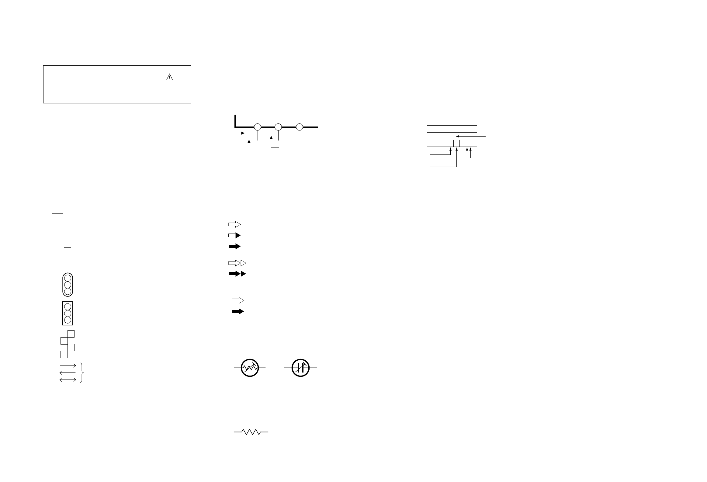
2. Indications of control voltage
AUX : Active at high.
AUX or AUX(L) : Active at low.
3. Interpreting Connector indications
1
2
Removable connector
3
1
2
Wire soldered directly on board
3
1
Non-removable Board connector
2
3
1
2
4
Board to Board
3
5. Signal path Symbols
The arrows indicate the signal path as follows.
NOTE : The arrow is DVC unique object.
Playback signal path
Playback and recording signal path
Recording signal path
(including E-E signal path)
Capstan servo path
Drum servo path
(Example)
R-Y
Playback R-Y signal path
Y
Recording Y signal path
6. Indication of the parts for adjustments
The parts for the adjustments are surrounded with the circle as
shown below.
Note: For g eneral information in service manual, please
refer to the Service Manual of GENERAL INFORMATION Edition 4 No. 82054D (January 1994).
S40889-01
Connected pattern on board
The arrows indicate signal path
7. Indication of the parts not mounted on the circuit board
“OPEN” is indicated by the parts not mounted on the circuit
board.
R216
OPEN
4-1
4-2
4-1 4-2
S40889-01
Page 2
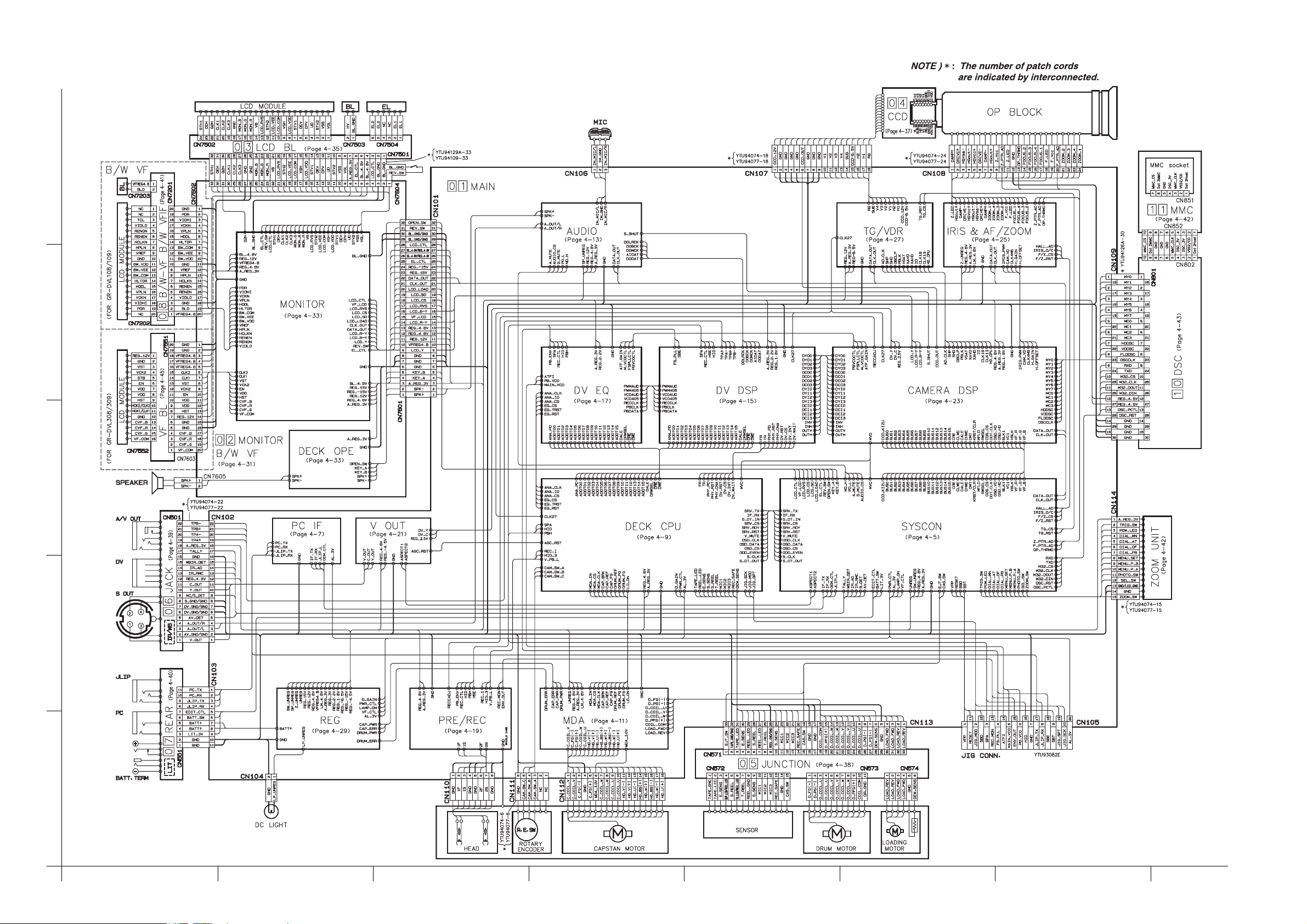
4.1 BOARD INTERCONNECTIONS
5
4
3
2
1
A
B
C
DEF
4-3
4-4
G
H
Page 3
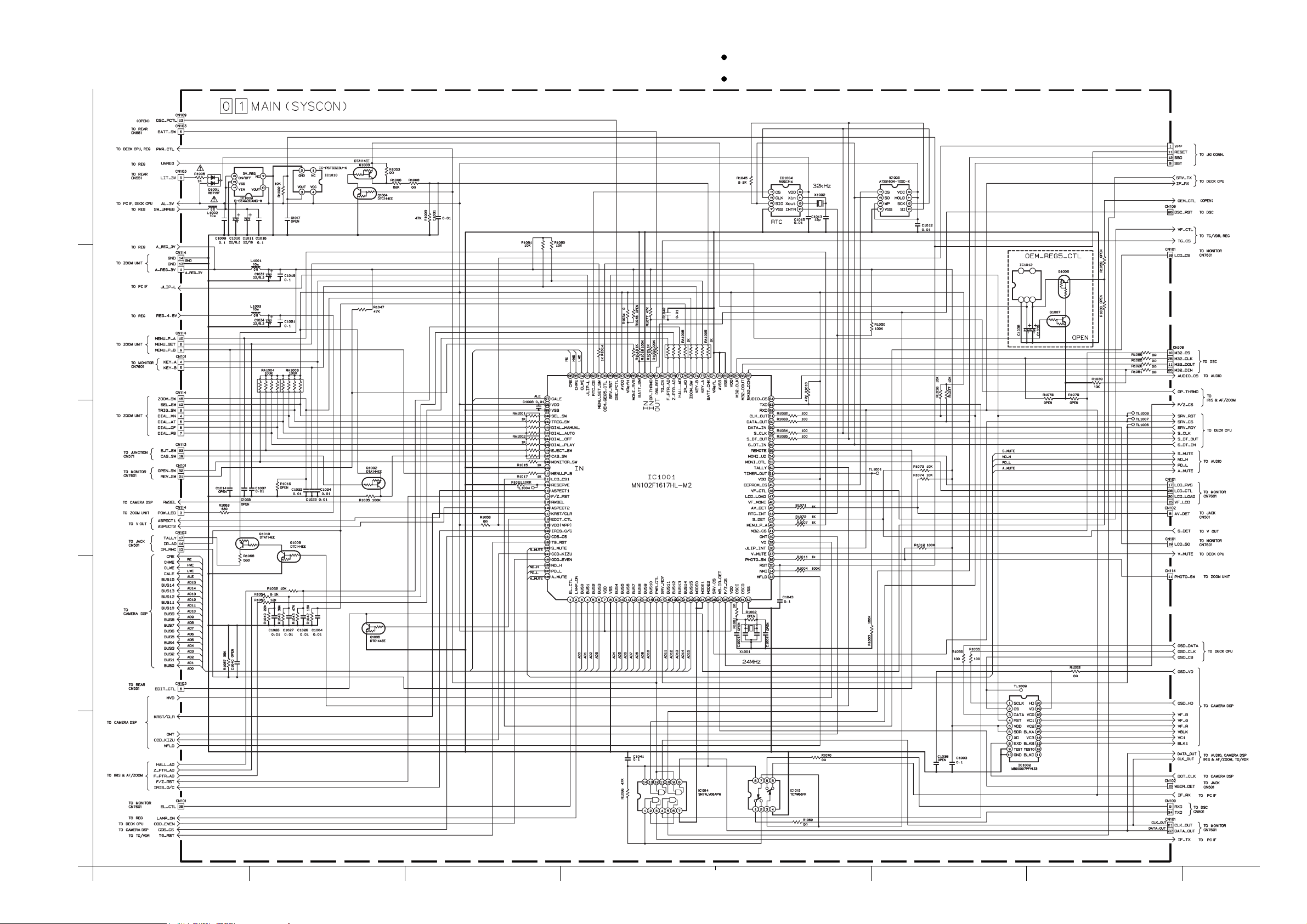
4.2 SYSCON SCHEMATIC DIAGRAM
5
4
NOTES: For the destination of each signal and further line connections that are cut off from
this diagram, refer to “4.1 BOARD INTERCONNECTIONS”.
When ordering parts, be sure to order according to the Part Number indicated in the Parts List.
3
2
1
A
B
C
DEF
4-5 4-6
G
H
Page 4
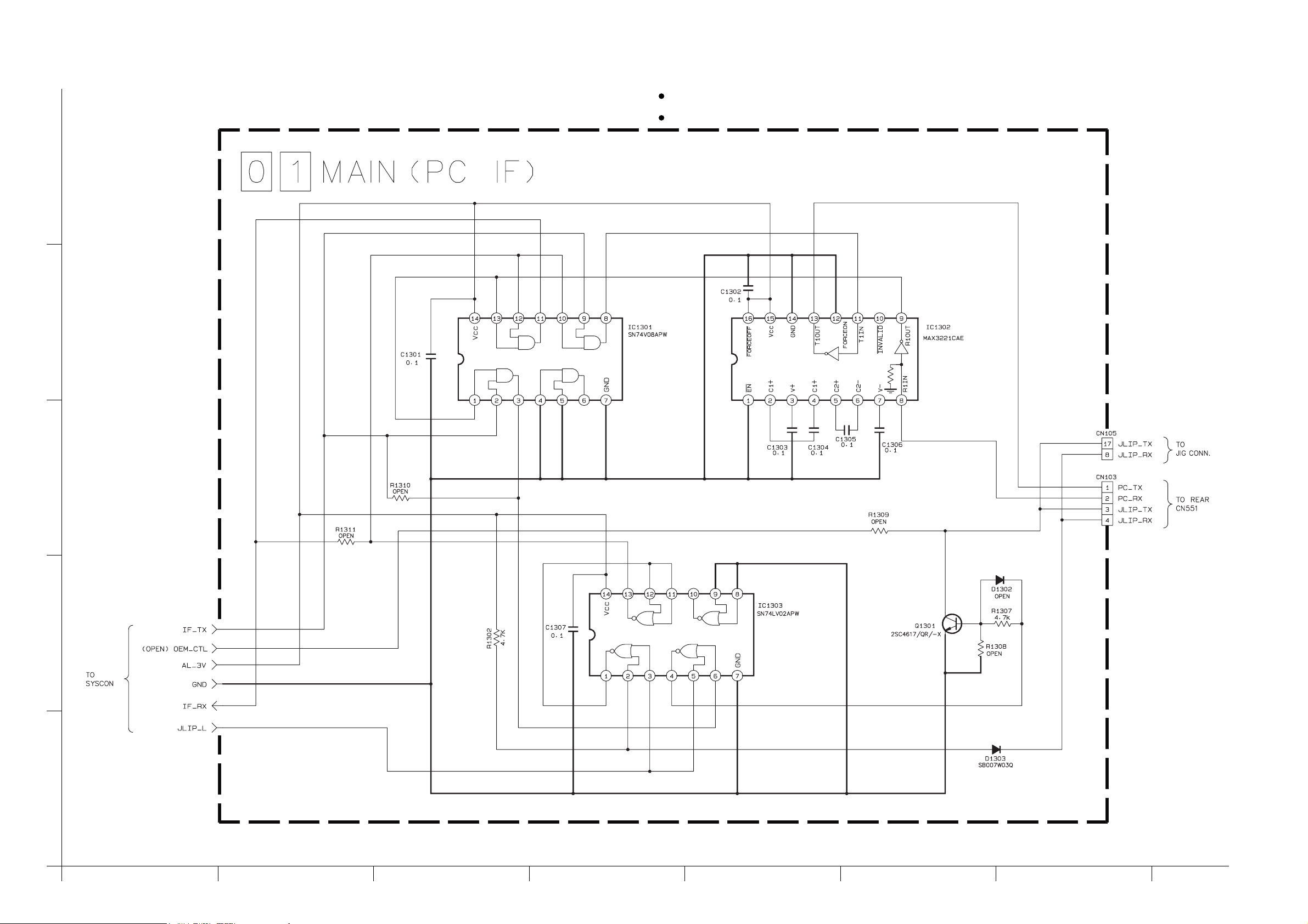
4.3 PC IF SCHEMATIC DIAGRAM
NOTES: For the destination of each signal and further line connections that are cut off from
this diagram, refer to “4.1 BOARD INTERCONNECTIONS”.
When ordering parts, be sure to order according to the Part Number indicated in the Parts List.
5
4
3
2
1
A
B
C
DEF
4-7
4-8
G
H
Page 5
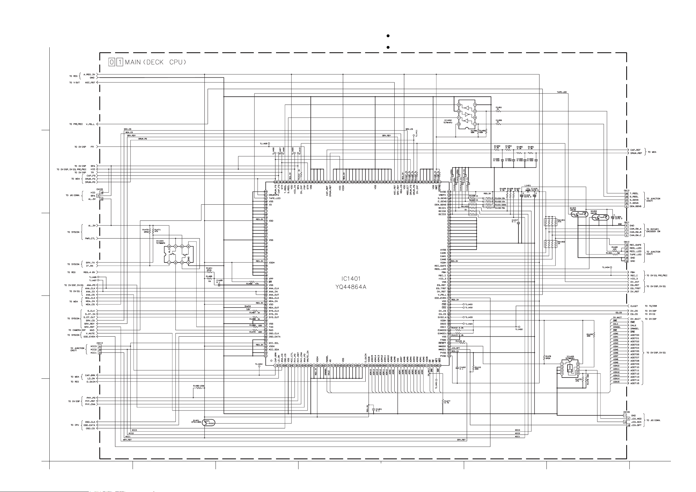
4.4 DECK CPU SCHEMATIC DIAGRAM
5
4
NOTES: For the destination of each signal and further line connections that are cut off from
this diagram, refer to “4.1 BOARD INTERCONNECTIONS”.
When ordering parts, be sure to order according to the Part Number indicated in the Parts List.
3
2
1
A
B
C
DEF
4-9
4-10
G
H
Page 6
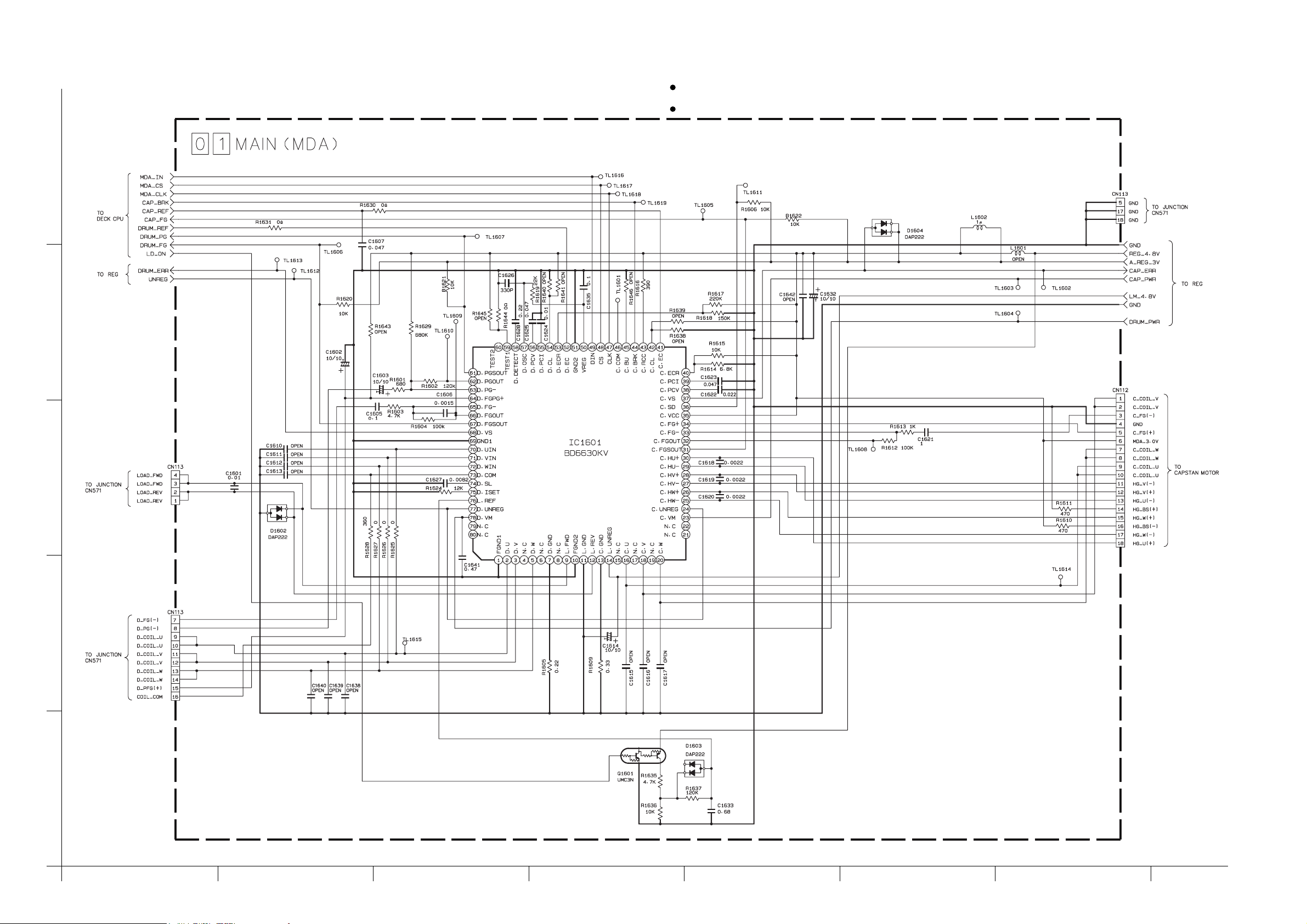
4.5 MDA SCHEMATIC DIAGRAM
5
4
NOTES: For the destination of each signal and further line connections that are cut off from
this diagram, refer to “4.1 BOARD INTERCONNECTIONS”.
When ordering parts, be sure to order according to the Part Number indicated in the Parts List.
3
2
1
A
B
C
DEF
4-11 4-12
G
H
Page 7
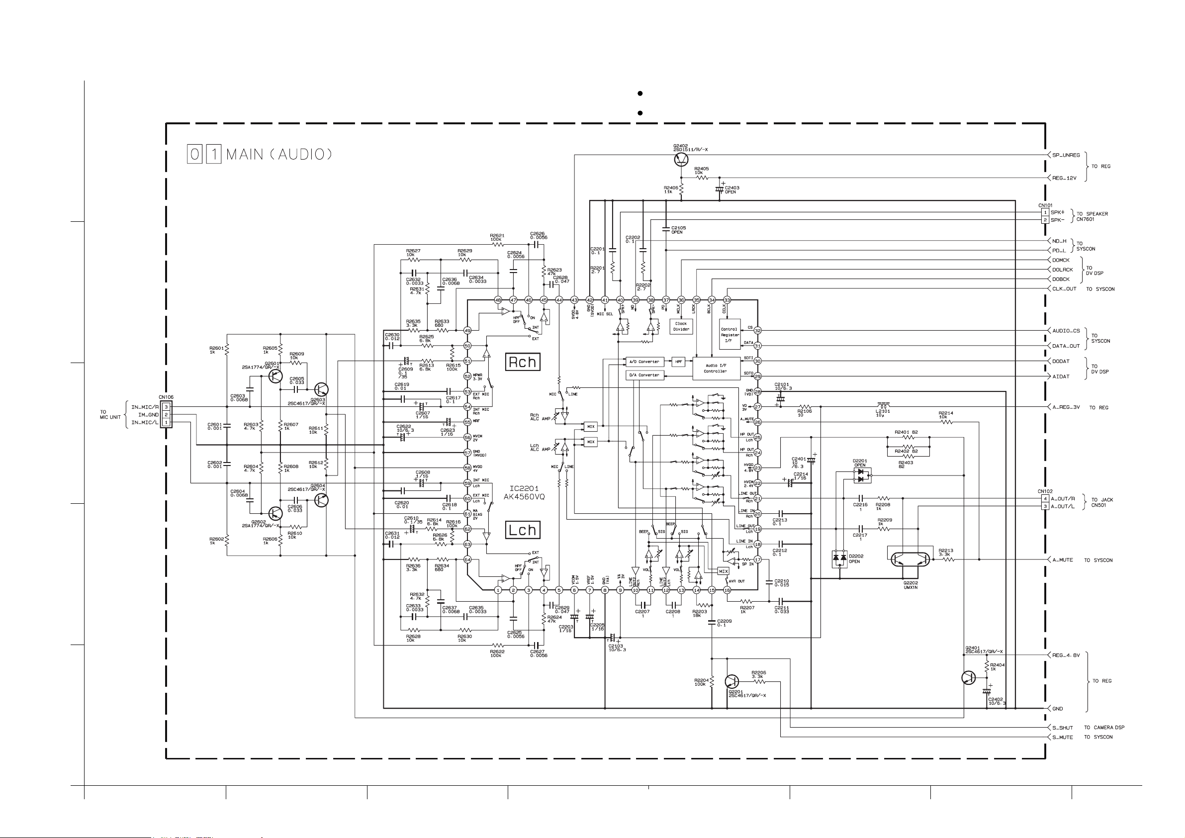
4.6 AUDIO SCHEMATIC DIAGRAM
NOTES: For the destination of each signal and further line connections that are cut off from
this diagram, refer to “4.1 BOARD INTERCONNECTIONS”.
When ordering parts, be sure to order according to the Part Number indicated in the Parts List.
5
4
3
2
1
A
B
C
DEF
4-13
4-14
G
H
Page 8
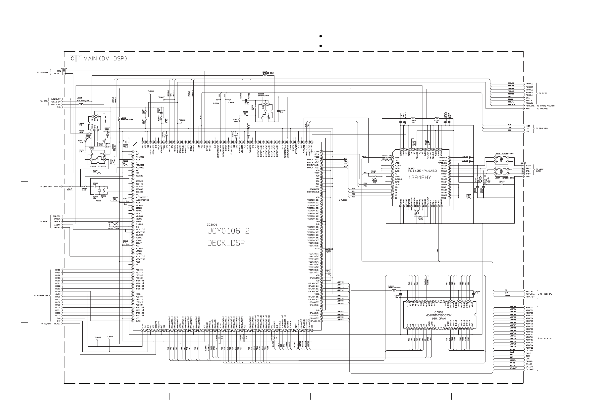
4.7 DV DSP SCHEMATIC DIAGRAM
5
4
NOTES: For the destination of each signal and further line connections that are cut off from
this diagram, refer to “4.1 BOARD INTERCONNECTIONS”.
When ordering parts, be sure to order according to the Part Number indicated in the Parts List.
3
2
1
A
B
C
DEF
4-15
4-16
G
H
Page 9
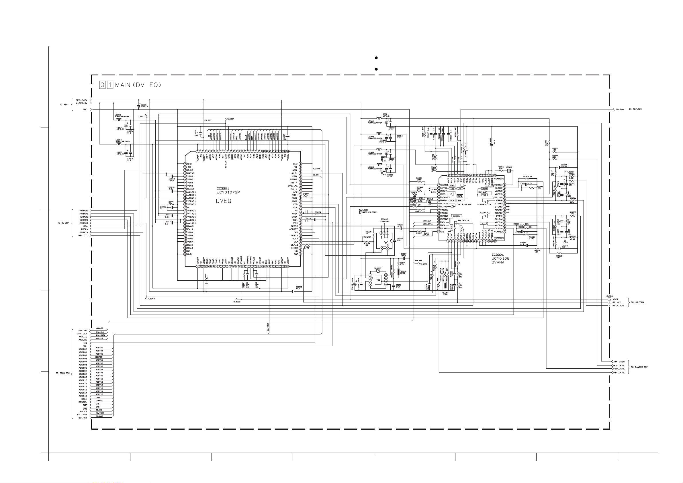
4.8 DV EQ SCHEMATIC DIAGRAM
5
4
NOTES: For the destination of each signal and further line connections that are cut off from
this diagram, refer to “4.1 BOARD INTERCONNECTIONS”.
When ordering parts, be sure to order according to the Part Number indicated in the Parts List.
3
2
1
A
B
C
DEF
4-17
4-18
G
H
Page 10
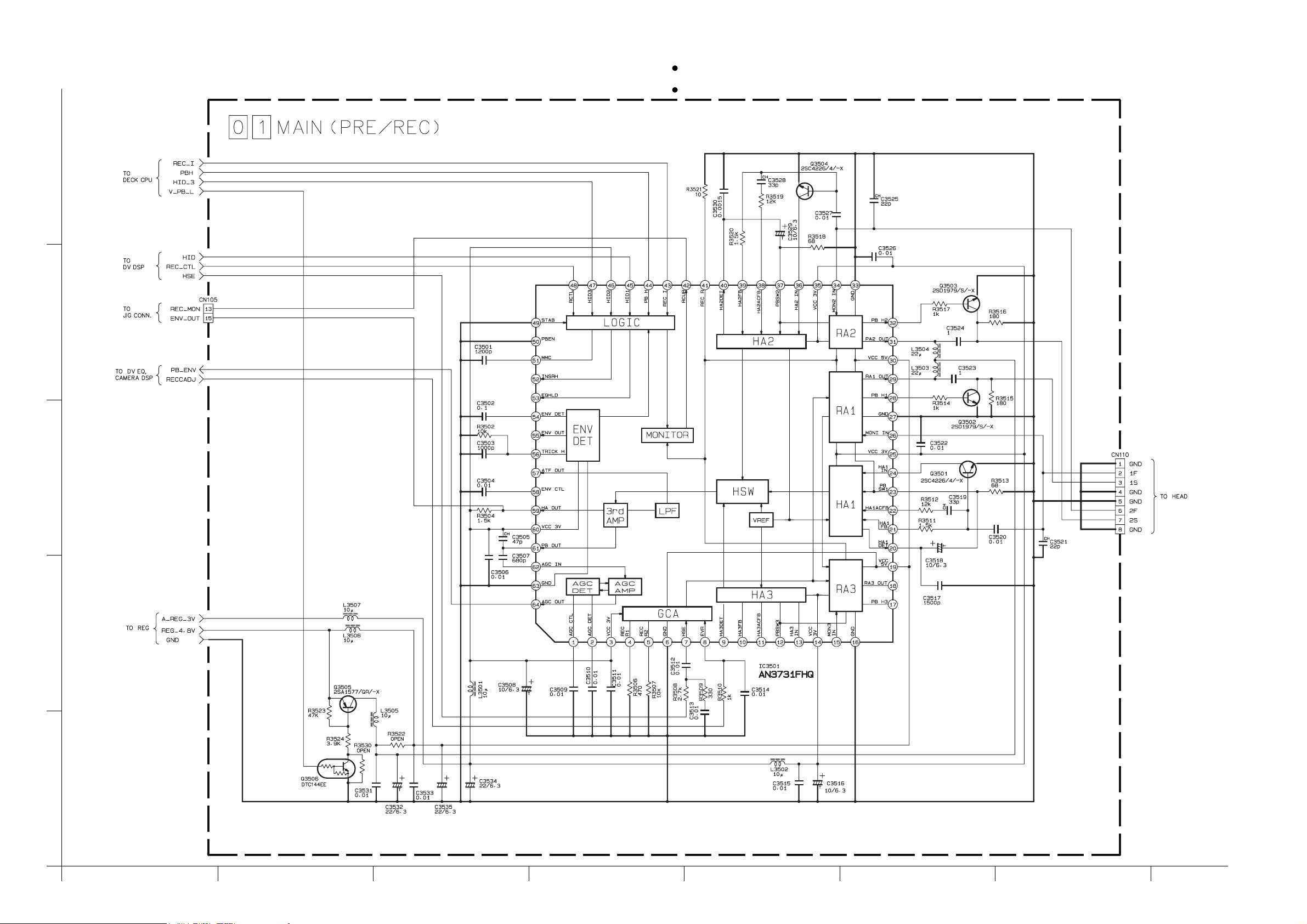
4.9 PRE/REC SCHEMATIC DIAGRAM
5
4
NOTES: For the destination of each signal and further line connections that are cut off from
this diagram, refer to “4.1 BOARD INTERCONNECTIONS”.
When ordering parts, be sure to order according to the Part Number indicated in the Parts List.
3
2
1
A
B
C
DEF
4-204-19
G
H
Page 11
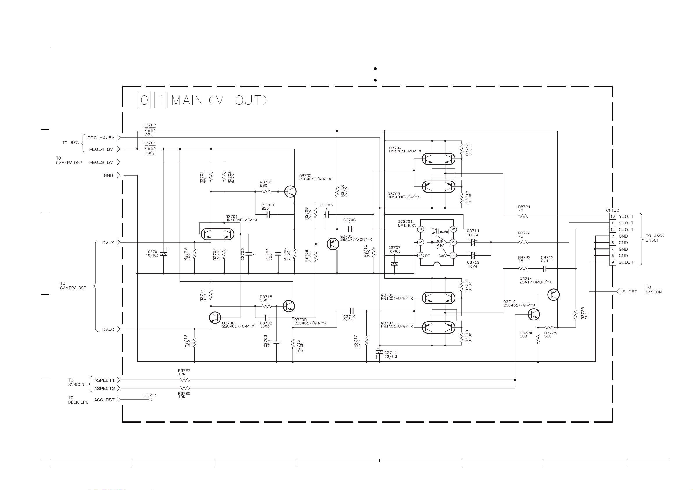
4.10 V OUT SCHEMATIC DIAGRAM
NOTES: For the destination of each signal and further line connections that are cut off from
this diagram, refer to “4.1 BOARD INTERCONNECTIONS”.
When ordering parts, be sure to order according to the Part Number indicated in the Parts List.
5
4
3
2
1
A
B
C
DEF
4-21 4-22
G
H
Page 12
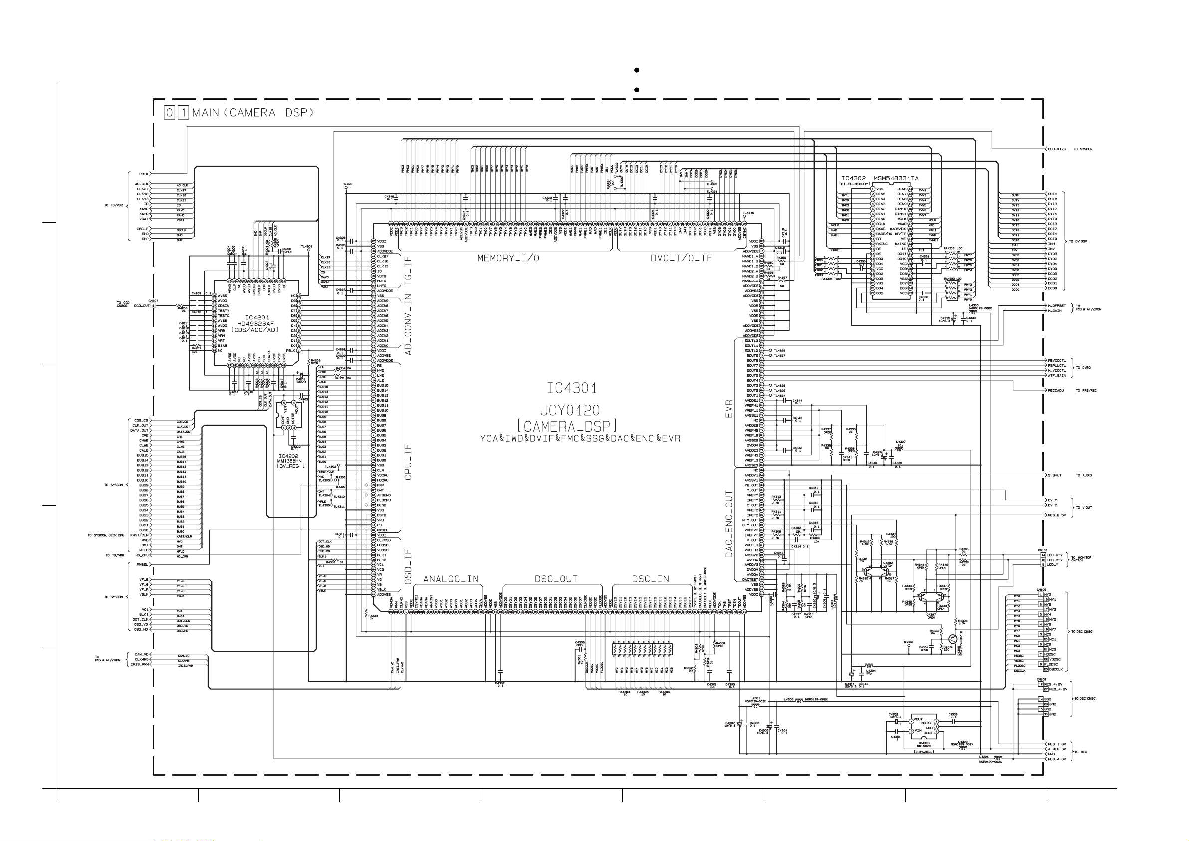
4.11 CAMERA DSP SCHEMATIC DIAGRAM
5
4
NOTES: For the destination of each signal and further line connections that are cut off from
this diagram, refer to “4.1 BOARD INTERCONNECTIONS”.
When ordering parts, be sure to order according to the Part Number indicated in the Parts List.
3
2
1
A
B
C
DEF
4-23
4-24
G
H
Page 13
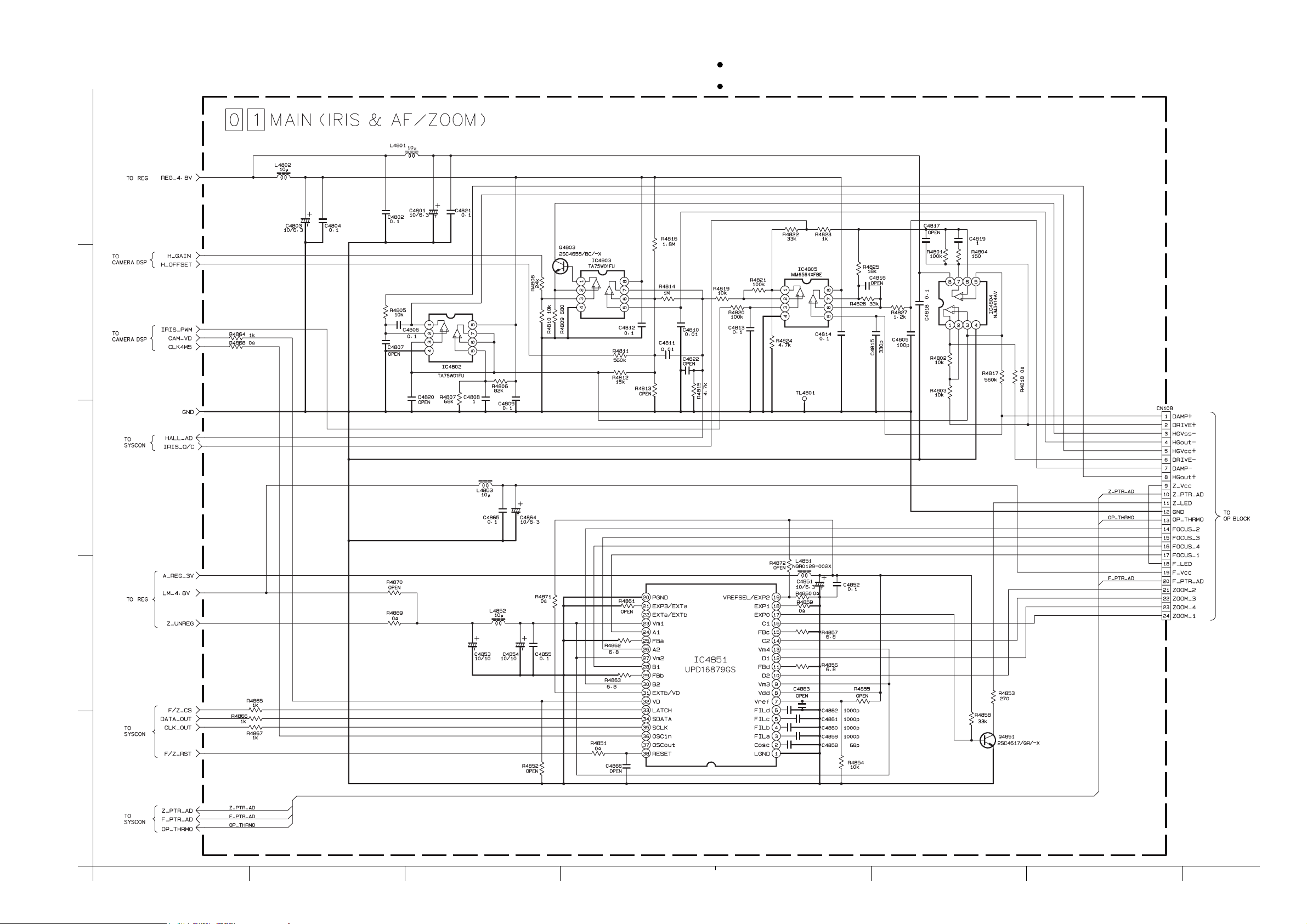
4.12 IRIS & AF/ZOOM SCHEMATIC DIAGRAM
5
4
NOTES: For the destination of each signal and further line connections that are cut off from
this diagram, refer to “4.1 BOARD INTERCONNECTIONS”.
When ordering parts, be sure to order according to the Part Number indicated in the Parts List.
3
2
1
A
B
C
DEF
4-25 4-26
G
H
Page 14
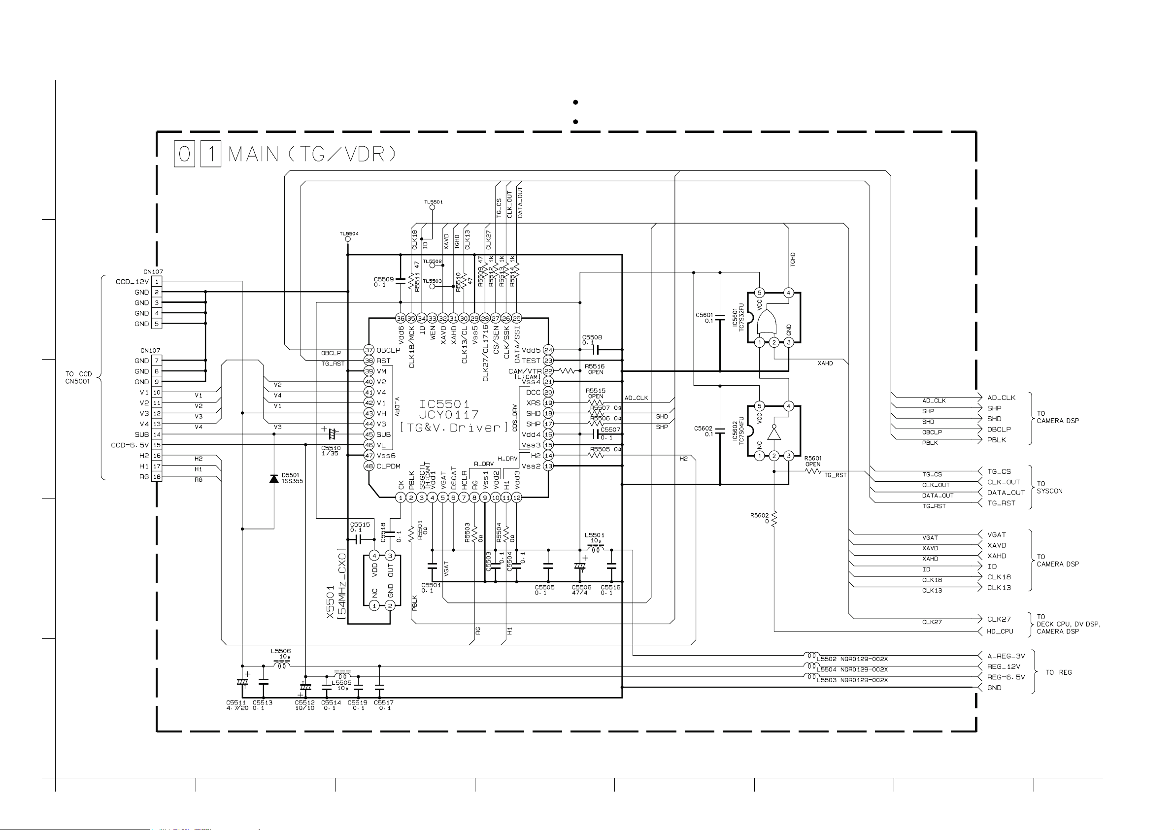
4.13 TG/VDR SCHEMATIC DIAGRAM
5
4
NOTES: For the destination of each signal and further line connections that are cut off from
this diagram, refer to “4.1 BOARD INTERCONNECTIONS”.
When ordering parts, be sure to order according to the Part Number indicated in the Parts List.
3
2
1
A
B
C
DEF
4-27
4-28
G
H
Page 15

4.14 REGULATOR SCHEMATIC DIAGRAM
5
4
NOTES: For the destination of each signal and further line connections that are cut off from
this diagram, refer to “4.1 BOARD INTERCONNECTIONS”.
When ordering parts, be sure to order according to the Part Number indicated in the Parts List.
3
2
1
A
B
C
DEF
4-29 4-30
G
H
Page 16

4.15 B/W VF SCHEMATIC DIAGRAM
(FOR DVL108/DVL109)
NOTES: For the destination of each signal and further line connections that are cut off from
this diagram, refer to “4.1 BOARD INTERCONNECTIONS”.
When ordering parts, be sure to order according to the Part Number indicated in the Parts List.
5
4
3
2
1
A
B
C
DEF
4-31 4-32
G
H
Page 17

4.16 MONITOR SCHEMATIC DIAGRAM
5
4
NOTES: For the destination of each signal and further line connections that are cut off from
this diagram, refer to “4.1 BOARD INTERCONNECTIONS”.
When ordering parts, be sure to order according to the Part Number indicated in the Parts List.
3
2
1
A
B
C
DEF
4-33 4-34
G
H
Page 18

4.17 LCD BL SCHEMATIC DIAGRAM
5
4
NOTES: For the destination of each signal and further line connections that are cut off from
this diagram, refer to “4.1 BOARD INTERCONNECTIONS”.
When ordering parts, be sure to order according to the Part Number indicated in the Parts List.
3
2
1
A
B
C
DEF
4-35
4-36
G
H
Page 19

4.18 CCD AND JUNCTION SCHEMATIC DIAGRAMS
NOTES: For the destination of each signal and further line connections that are cut off from
this diagram, refer to “4.1 BOARD INTERCONNECTIONS”.
When ordering parts, be sure to order according to the Part Number indicated in the Parts List.
5
— JUNCTION —
— CCD —
4
3
2
1
A
B
C
DEF
4-37
4-38
G
H
Page 20

4.19 JACK AND REAR SCHEMATIC DIAGRAMS
NOTES: For the destination of each signal and further line connections that are cut off from
— JACK —
this diagram, refer to “4.1 BOARD INTERCONNECTIONS”.
When ordering parts, be sure to order according to the Part Number indicated in the Parts List.
5
— REAR —
4
3
2
1
A
B
C
DEF
4-39
4-40
G
H
Page 21

4.20 B/W VFIF,MMC AND ZOOM UNIT SCHEMATIC DIAGRAMS
— B/W VFIF —
5
(FOR DVL108/DVL109)
4
NOTES: For the destination of each signal and further line connections that are cut off from
this diagram, refer to “4.1 BOARD INTERCONNECTIONS”.
When ordering parts, be sure to order according to the Part Number indicated in the Parts List.
— MMC —
NOTES: For the destination of each signal and further line connections that are cut off from
3
this diagram, refer to “4.1 BOARD INTERCONNECTIONS”.
The schematic diagram is only for reference. Avoid replacing individual parts.
Replace the entire unit only.
— ZOOM UNIT —
2
1
A
B
C
DEF
4-41 4-42
G
H
Page 22

4.21 DSC SCHEMATIC DIAGRAM
NOTES: For the destination of each signal and further line connections that are cut off from
this diagram, refer to “4.1 BOARD INTERCONNECTIONS”.
When ordering parts, be sure to order according to the Part Number indicated in the Parts List.
5
4
3
2
1
A
B
C
DEF
4-43 4-44
G
H
Page 23

4.22 VF BL SCHEMATIC DIAGRAM
(FOR DVL308/DVL309)
5
4
NOTES: For the destination of each signal and further line connections that are cut off from
this diagram, refer to “4.1 BOARD INTERCONNECTIONS”.
The schematic diagram is only for reference. Avoid replacing individual parts.
Replace the entire unit only.
3
2
1
A
B
C
DEF
4-45
4-46
G
H
Page 24

4.23 MAIN CIRCUIT BOARD
5
4
FOIL SIDE (B)
3
2
1
A
B
C
DEF
4-47 4-48
G
H
Page 25

COMPONENT PARTS LOCATION GUIDE (MAIN)
REF.No. LOCATION
CAPACITOR
C1001 B C 3C
C1002 B C 3B
C1003 B C 3A
C1004 B C 4A
C1008 B C 2B
C1009 B C 3B
C1010 B C 3B
C1011 B C 3A
C1012 B C 2C
C1013 B C 1C
C1014 B C 2B
C1015 B C 1C
C1016 B C 3A
C1017 B C 4A
C1019 B C 1B
C1021 B C 2B
C1022 B C 4B
C1023 B C 4B
C1024 B C 4B
C1026 B C 4A
C1027 B C 4A
C1028 B C 4A
C1031 B C 4B
C1032 B C 2B
C1034 B C 1B
C1035 B C 3B
C1036 B C 4A
C1037 B C 1A
C1038 B C 3A
C1039 B C 3A
C1040 B C 2B
C1041 B C 4A
C1042 B C 2B
C1043 B C 3C
C1301 B C 3C
C1302 B C 3B
C1303 B C 3B
C1304 B C 3B
C1305 B C 3B
C1306 B C 3B
C1307 B C 4C
C1401 A C 2B
C1402 A C 2B
C1411 A C 2B
C1412 A C 2B
C1413 A C 2B
C1414 A C 2B
C1415 A C 2B
C1416 A C 2B
C1417 A C 2B
C1418 B C 1B
C1419 B C 1B
C1420 A C 3A
C1421 A C 3A
C1422 A C 3B
C1423 A C 3B
C1424 B C 1B
C1425 A C 3B
C1601 A C 1B
C1602 A C 1B
C1603 A C 1B
C1605 A C 1A
C1606 A C 1B
C1607 A C 1B
C1610 A C 1A
C1611 A C 1A
C1612 A C 1A
C1613 A C 1A
C1614 A C 1C
C1615 A C 1B
C1616 A C 1B
C1617 A C 1B
C1618 A C 1B
C1619 A C 1B
C1620 A C 1B
C1621 A C 1B
C1622 A C 1B
C1623 A C 1B
C1624 A C 1B
C1625 A C 1B
C1626 A C 1B
C1627 A C 1A
C1628 A C 1B
C1632 A C 1B
C1633 A C 2B
C1635 A C 2B
C1638 A C 1A
C1639 A C 1A
C1640 A C 1B
C1641 A C 1B
C1642 A C 1A
C2101 B C 5C
C2103 B C 4C
C2105 B C 5C
C2201 B C 5C
C2202 B C 5C
C2203 B C 4C
C2205 B C 4C
C2207 B C 4C
C2208 B C 4C
C2209 B C 4C
C2210 B C 4C
C2211 B C 4C
C2212 B C 4C
C2213 B C 4C
C2214 B C 5C
C2216 B C 4C
C2217 B C 4C
C2401 B C 5C
C2402 B C 4D
C2403 B C 5C
C2601 B C 4D
C2602 B C 4D
C2603 B C 4D
C2604 B C 4D
C2605 B C 4D
REF.No. LOCATION REF.No. LOCATION
C2606 B C 4D
C2607 B C 5C
C2608 B C 4C
C2609 B C 5C
C2610 B C 4C
C2617 B C 5C
C2618 B C 5C
C2619 B C 4D
C2620 B C 4C
C2622 B C 4C
C2623 B C 4C
C2624 B C 5C
C2625 B C 4C
C2626 B C 5C
C2627 B C 4C
C2628 B C 5C
C2629 B C 4C
C2630 B C 5D
C2631 B C 4C
C2632 B C 5C
C2633 B C 4C
C2634 B C 5C
C2635 B C 4C
C2636 B C 5C
C2637 B C 4C
C3001 A C 3B
C3002 A C 3B
C3003 A C 3B
C3004 A C 3B
C3005 A C 3B
C3006 A C 3C
C3007 A C 4C
C3009 A C 4B
C3010 A C 4B
C3011 A C 4B
C3012 A C 4B
C3022 A C 3B
C3023 A C 4B
C3027 A C 4C
C3028 A C 4C
C3035 A C 4B
C3037 A C 4B
C3038 A C 4C
C3040 A C 4B
C3041 A C 4B
C3042 A C 4B
C3047 A C 4C
C3048 A C 4C
C3049 A C 4B
C3050 A C 4B
C3101 A C 5C
C3102 A C 5C
C3103 A C 5C
C3104 A C 5C
C3105 A C 5C
C3106 A C 5C
C3107 A C 5C
C3108 A C 4C
C3109 A C 5C
C3203 A C 3C
C3204 A C 3C
C3205 A C 3C
C3207 A C 3C
C3208 A C 3C
C3211 A C 3C
C3212 A C 3C
C3213 A C 3C
C3214 A C 2C
C3215 A C 2B
C3217 A C 3C
C3218 A C 3C
C3219 A C 2B
C3220 A C 3B
C3221 A C 4D
C3222 A C 2B
C3223 A C 2C
C3224 A C 2C
C3227 A C 3D
C3228 A C 3D
C3229 A C 3D
C3230 A C 3D
C3231 A C 4D
C3232 A C 4D
C3301 A C 3D
C3302 A C 3D
C3303 A C 4D
C3304 A C 4D
C3305 A C 3D
C3306 A C 3D
C3307 A C 4C
C3308 A C 4D
C3309 A C 3D
C3310 A C 3D
C3311 A C 4D
C3312 A C 4D
C3313 A C 4D
C3314 A C 4D
C3316 A C 4D
C3317 A C 4D
C3318 A C 4D
C3319 A C 4D
C3320 A C 4D
C3321 A C 3C
C3322 A C 3D
C3323 A C 3D
C3324 A C 3C
C3326 A C 3D
C3327 A C 3D
C3328 A C 4D
C3331 A C 3D
C3332 A C 3D
C3333 A C 3D
C3334 A C 3D
C3335 A C 3D
C3336 A C 3D
C3337 A C 3D
C3501 B C 3C
C3502 B C 3C
C3503 B C 3C
C3504 B C 3C
C3505 B C 3C
C3506 B C 3C
C3507 B C 3C
C3508 B C 3C
C3509 B C 3C
C3510 B C 3C
C3511 B C 3C
C3512 B C 3C
C3513 B C 4C
C3514 B C 3C
C3515 B C 3C
C3516 B C 3C
C3517 B C 3C
C3518 B C 3C
C3519 B C 3D
C3520 B C 3D
C3521 B C 3D
C3522 B C 3C
C3523 B C 3D
C3524 B C 3D
C3525 B C 3C
C3526 B C 3C
C3527 B C 3C
C3528 B C 3C
C3529 B C 3C
C3530 B C 3C
C3531 B C 3C
C3532 B C 3D
C3533 B C 3C
C3534 B C 4D
C3535 B C 4C
C3701 A C 5A
C3702 A C 5A
C3703 A C 5B
C3704 A C 5B
C3705 A C 5A
C3706 A C 5B
C3707 A C 5B
C3708 A C 5A
C3709 A C 5B
C3710 A C 5B
C3711 A C 5B
C3712 A C 5B
C3713 A C 5B
C3714 A C 5B
C4201 A C 5A
C4202 A C 5A
C4203 A C 5A
C4204 A C 5A
C4205 A C 5A
C4206 A C 5A
C4207 A C 5A
C4208 A C 5A
C4209 A C 4A
C4210 A C 5A
C4211 A C 5A
C4212 A C 5A
C4213 A C 5A
C4214 A C 5A
C4215 A C 4A
C4216 A C 5A
C4217 A C 4A
C4301 A C 3B
C4302 A C 3A
C4303 A C 4B
C4304 A C 3B
C4305 A C 3B
C4306 A C 3B
C4307 A C 3B
C4308 A C 4A
C4309 A C 4A
C4310 A C 5A
C4311 A C 5B
C4312 A C 4B
C4313 A C 4A
C4314 A C 4B
C4315 A C 4A
C4316 A C 4A
C4317 A C 4A
C4318 A C 4B
C4319 A C 3A
C4320 A C 4B
C4321 A C 3A
C4322 A C 4A
C4323 A C 3A
C4324 A C 4A
C4325 A C 4B
C4326 A C 4A
C4327 A C 3B
C4328 A C 3B
C4329 A C 3B
C4330 A C 2A
C4331 A C 3A
C4332 A C 3A
C4333 A C 2A
C4334 A C 4B
C4335 A C 3A
C4336 A C 3A
C4337 A C 4A
C4338 A C 3A
C4339 A C 3A
C4340 A C 3A
C4341 A C 3A
C4342 A C 3A
C4343 A C 3A
C4344 A C 3A
C4345 A C 3A
C4346 A C 4A
C4347 A C 4A
C4351 A C 3B
C4352 A C 3B
C4353 A C 3B
C4801 B C 5A
C4802 B C 5A
REF.No. LOCATION
C4803 A C 5A
C4804 A C 5A
C4805 B C 5A
C4806 B C 5B
C4807 B C 5B
C4808 B C 5B
C4809 B C 5B
C4810 B C 5B
C4811 B C 5B
C4812 B C 5B
C4813 B C 5A
C4814 A C 5A
C4815 B C 5A
C4816 B C 5A
C4817 B C 5B
C4818 B C 5B
C4819 B C 5B
C4820 B C 5B
C4821 B C 5A
C4822 B C 5B
C4851 B C 4B
C4852 B C 4B
C4853 B C 3B
C4854 B C 4B
C4855 B C 4B
C4858 B C 4B
C4859 B C 4B
C4860 B C 4B
C4861 B C 4B
C4862 B C 4B
C4863 B C 4B
C4864 B C 5A
C4865 B C 5A
C4866 B C 4B
C5501 B C 3A
C5503 B C 2A
C5504 B C 3A
C5505 B C 2B
C5506 B C 2A
C5507 B C 3A
C5508 B C 3A
C5509 B C 3A
C5510 B C 3A
C5511 B C 3A
C5512 B C 2A
C5513 B C 4A
C5514 B C 3A
C5515 B C 2A
C5516 B C 2B
C5517 B C 4A
C5518 B C 3A
C5519 B C 2A
C5601 A C 2B
C5602 A C 2B
C6001 B C 1C
C6002 B C 1D
C6003 B C 2D
C6004 A C 2D
C6005 A C 2D
C6006 A C 2D
C6007 A C 2D
C6008 A C 2D
C6009 A C 2D
C6010 A C 2D
C6011 A C 2D
C6012 A C 2D
C6013 A C 2D
C6014 A C 2D
C6015 A C 2D
C6016 A C 2D
C6017 A C 3D
C6018 A C 3D
C6019 A C 3D
C6022 A C 2D
C6111 B C 2C
C6113 A C 2C
C6114 A C 2C
C6121 B C 1C
C6123 A C 1C
C6124 A C 1C
C6125 B C 1D
C6126 B C 1C
C6127 B C 1C
C6131 B C 2C
C6132 A C 1C
C6133 A C 2D
C6134 B C 1C
C6141 A C 1C
C6142 A C 1C
C6143 A C 1C
C6144 B C 2C
C6151 A C 2C
C6153 B C 2C
C6154 B C 1C
C6155 B C 2C
C6157 B C 2C
C6161 A C 2D
C6162 B C 2C
C6163 B C 3C
C6164 B C 2C
C6165 B C 2C
C6167 B C 2C
C6168 B C 2C
C6169 B C 2C
C6171 B C 2C
C6173 B C 2C
C6174 B C 2C
C6175 B C 2C
C6201 B C 2D
C6301 A C 3D
C6302 A C 3C
C6401 B C 2C
C6402 B C 1C
CONNECTOR
CN101 B C 4D
CN102 A C 4D
REF.No. LOCATION REF.No. LOCATION
CN103 B C 1D
CN104 B C 5C
CN105 B C 1B
CN106 B C 4D
CN107 B C 3A
CN108 B C 5B
CN109 B C 1C
CN110 B C 3D
CN111 A C 5B
CN112 A C 1D
CN113 B C 2D
CN114 B C 1B
DIODE
D1001 B C 1C
D1302 B C 4B
D1303 B C 4C
D1602 A C 1C
D1603 A C 2B
D1604 A C 1B
D2201 B C 4C
D2202 B C 4C
D5501 B C 3A
D6111 B C 2C
D6121 B C 1D
D6122 B C 1C
D6131 B C 2C
D6141 A C 1C
D6151 A C 2B
D6152 B C 2C
D6161 B C 2C
D6163 B C 2C
D6165 B C 2C
FUSE
F6001 B C 1C
F6003 A C 1C
F6004 A C 1C
F6005 A C 2D
IC
IC1001 B C 2B
IC1002 B C 3A
IC1003 B C 2C
IC1004 B C 2C
IC1009 B C 3A
IC1010 B C 4A
IC1012 B C 3A
IC1014 B C 3B
IC1015 B C 4B
IC1301 B C 4B
IC1302 B C 3B
IC1303 B C 4C
IC1401 A C 2B
IC1402 B C 1A
IC1403 B C 1B
IC1405 B C 1B
IC1601 A C 1B
IC2201 B C 5C
IC3001 A C 4B
IC3002 A C 4C
IC3004 A C 3B
IC3005 A C 4B
IC3007 A C 3C
IC3101 A C 5C
IC3201 A C 2C
IC3202 A C 4D
IC3203 A C 3D
IC3301 A C 4D
IC3501 B C 3C
IC3701 A C 5B
IC4201 A C 4A
IC4202 A C 5A
IC4301 A C 3A
IC4302 A C 3A
IC4303 A C 3B
IC4802 B C 5B
IC4803 B C 5B
IC4804 B C 5B
IC4805 A C 5A
IC4851 B C 4B
IC5501 B C 3A
IC5601 A C 2A
IC5602 A C 2A
IC6001 A C 2D
IC6301 A C 3D
COIL
L1001 B C 2A
L1002 B C 3A
L1003 B C 1B
L1401 B C 1B
L1601 A C 1B
L1602 A C 1C
L2101 B C 5C
L3001 A C 4C
L3002 A C 3B
L3004 A C 4C
L3005 A C 3C
L3101 A C 5C
L3102 A C 5C
L3103 A C 5C
L3104 A C 5C
L3202 A C 3C
L3203 A C 3D
L3204 A C 3B
L3301 A C 3D
L3302 A C 4D
L3303 A C 3D
L3304 A C 4D
L3501 B C 3C
L3502 B C 3D
L3503 B C 3D
L3504 B C 3D
L3505 B C 3D
L3506 B C 4D
L3507 B C 4D
L3701 A C 5A
L3702 A C 5B
L4201 A C 5A
L4301 A C 3B
L4302 A C 3B
L4303 A C 5A
L4304 A C 5B
L4305 A C 2A
L4306 A C 3B
L4307 A C 3A
L4801 B C 5A
L4802 A C 5A
L4851 B C 4B
L4852 B C 4B
L4853 B C 5A
L5501 B C 2A
L5502 B C 2A
L5503 B C 2A
L5504 B C 4A
L5505 B C 2A
L5506 B C 3A
L6001 B C 2D
L6002 B C 2D
L6111 A C 1C
L6114 B C 1C
L6121 A C 1D
L6123 B C 1C
L6124 B C 1C
L6131 A C 1C
L6141 A C 1C
L6151 A C 2C
L6161 A C 2C
L6202 A C 1D
L6401 B C 2D
TRANSISTOR
TRANSISTOR
Q1002 B C 4A
Q1003 B C 4A
Q1004 B C 4A
Q1006 B C 4A
Q1007 B C 4A
Q1008 B C 4A
Q1009 B C 2C
Q1010 B C 2C
Q1301 B C 3B
Q1401 A C 2B
Q1402 B C 1B
Q1403 B C 1B
Q1601 A C 2B
Q2201 B C 4C
Q2202 B C 4C
Q2401 B C 4D
Q2402 B C 5C
Q2601 B C 4D
Q2602 B C 4D
Q2603 B C 4D
Q2604 B C 5D
Q3501 B C 3D
Q3502 B C 3D
Q3503 B C 3D
Q3504 B C 3C
Q3505 B C 3D
Q3506 B C 3D
Q3701 A C 5A
Q3702 A C 5A
Q3703 A C 5B
Q3704 A C 5B
Q3705 A C 5B
Q3706 A C 5B
Q3707 A C 5B
Q3708 A C 5A
Q3709 A C 5B
Q3710 A C 5B
Q3711 A C 5B
Q4302 A C 4B
Q4306 A C 4B
Q4307 A C 4B
Q4803 B C 5B
Q4851 B C 4B
Q6111 B C 2C
Q6112 B C 2C
Q6121 B C 1C
Q6122 B C 1C
Q6123 A C 1D
Q6124 B C 1D
Q6131 B C 2C
Q6132 A C 2C
Q6141 A C 1C
Q6151 A C 2B
Q6161 A C 2D
Q6162 B C 3C
Q6163 B C 2C
Q6164 B C 3C
Q6165 B C 2C
Q6166 B C 2C
Q6167 B C 2C
Q6168 B C 2C
Q6201 A C 2C
Q6202 A C 2D
Q6203 A C 2C
Q6301 A C 3D
Q6302 A C 3D
Q6303 A C 3D
Q6304 A C 3D
Q6305 A C 2C
RESISTOR
R1001 B C 3C
R1002 B C 3B
R1003 B C 3C
R1004 B C 3C
R1005 B C 1C
R1006 B C 4A
R1007 B C 3B
R1008 B C 4A
R1009 B C 4B
R1010 B C 2C
4-49
Page 26

REF.No. LOCATION
R1011 B C 3C
R1012 B C 1A
R1013 B C 2B
R1014 B C 2B
R1015 B C 2B
R1016 B C 4B
R1017 B C 2B
R1018 B C 2B
R1021 B C 2B
R1022 B C 4A
R1025 B C 2B
R1026 B C 2B
R1030 B C 4A
R1034 B C 2B
R1035 B C 4A
R1037 B C 2C
R1038 B C 2C
R1039 B C 2C
R1042 B C 4A
R1043 B C 4A
R1045 B C 2C
R1046 B C 2B
R1047 B C 2B
R1048 B C 4A
R1049 B C 4A
R1050 B C 3C
R1051 B C 2C
R1052 B C 4A
R1053 B C 4A
R1054 B C 4A
R1055 B C 3A
R1056 B C 3A
R1057 B C 4A
R1058 B C 5B
R1059 B C 4A
R1060 B C 2B
R1062 B C 3A
R1063 B C 1B
R1065 B C 2B
R1066 B C 4B
R1067 B C 2B
R1068 B C 3C
R1069 B C 4B
R1070 B C 4B
R1071 B C 3B
R1072 B C 3B
R1073 B C 3B
R1074 B C 3B
R1076 B C 2B
R1077 B C 2B
R1078 B C 2B
R1079 B C 2B
R1080 B C 4A
R1081 B C 4A
R1082 B C 2C
R1083 B C 2C
R1084 B C 2C
R1085 B C 2C
R1302 B C 4C
R1307 B C 4B
R1308 B C 3B
R1309 B C 3B
R1310 B C 3B
R1311 B C 3C
R1401 B C 5C
R1408 B C 1B
R1410 A C 2B
R1412 A C 2B
R1413 A C 2B
R1414 A C 3B
R1415 A C 2B
R1420 B C 1B
R1427 A C 2B
R1428 A C 2B
R1429 A C 2B
R1430 A C 2B
R1431 A C 2B
R1432 A C 2B
R1433 A C 2B
R1434 A C 2B
R1435 A C 2B
R1438 A C 2A
R1439 A C 2A
R1444 A C 3B
R1445 A C 2B
R1446 A C 2A
R1447 A C 3B
R1450 A C 3B
R1451 A C 3B
R1452 A C 3A
R1453 A C 3A
R1458 B C 1A
R1459 B C 1A
R1460 B C 1A
R1461 B C 1A
R1464 B C 1B
R1465 B C 5C
R1466 A C 3B
R1467 A C 3B
R1468 A C 3B
R1469 A C 3B
R1470 A C 3B
R1471 B C 1B
R1472 B C 1B
R1474 A C 3B
R1475 B C 1B
R1476 B C 1B
R1477 A C 2B
R1478 B C 1B
R1480 A C 3B
R1601 A C 1B
R1602 A C 1B
R1603 A C 1A
R1604 A C 1B
R1605 A C 1C
R1606 A C 1B
R1609 A C 1C
R1610 A C 1D
REF.No. LOCATION REF.No. LOCATION
R1611 A C 2D
R1612 A C 1B
R1613 A C 1B
R1614 A C 1B
R1615 A C 1B
R1616 A C 1B
R1617 A C 1B
R1618 A C 1B
R1619 A C 1B
R1620 A C 1A
R1621 A C 1B
R1622 A C 1C
R1624 A C 1A
R1625 A C 1B
R1626 A C 1B
R1627 A C 1B
R1628 A C 1B
R1629 A C 1B
R1630 A C 1B
R1631 A C 2B
R1635 A C 2B
R1636 A C 2B
R1637 A C 2B
R1638 A C 1B
R1639 A C 1B
R1640 A C 1B
R1641 A C 1B
R1643 A C 1A
R1644 A C 1B
R1645 A C 1B
R1646 A C 1B
R2106 B C 5C
R2201 B C 5C
R2202 B C 5C
R2203 B C 4C
R2204 B C 4C
R2206 B C 4C
R2207 B C 4C
R2208 B C 4B
R2209 B C 4C
R2213 B C 4C
R2214 B C 4C
R2401 B C 4C
R2402 B C 4C
R2403 B C 4C
R2404 B C 5D
R2405 B C 5C
R2406 B C 5C
R2601 B C 4D
R2602 B C 4D
R2603 B C 4D
R2604 B C 4D
R2605 B C 4D
R2606 B C 4D
R2607 B C 4D
R2608 B C 4D
R2609 B C 4D
R2610 B C 4D
R2611 B C 4D
R2612 B C 5D
R2613 B C 5C
R2614 B C 4C
R2615 B C 5C
R2616 B C 4C
R2621 B C 5C
R2622 B C 4D
R2623 B C 5C
R2624 B C 4C
R2625 B C 5C
R2626 B C 4C
R2627 B C 5C
R2628 B C 4C
R2629 B C 5C
R2630 B C 4C
R2631 B C 5C
R2632 B C 4C
R2633 B C 5C
R2634 B C 4C
R2635 B C 5C
R2636 B C 4C
R3002 A C 4B
R3005 A C 3B
R3006 A C 3B
R3007 A C 4B
R3008 A C 3C
R3030 A C 3C
R3031 A C 3C
R3032 A C 3C
R3047 A C 4B
R3052 A C 4B
R3054 A C 4B
R3055 A C 4B
R3056 A C 4B
R3057 A C 4B
R3058 A C 4B
R3059 A C 4B
R3060 A C 3C
R3062 A C 4B
R3063 A C 4B
R3101 A C 5B
R3102 A C 5B
R3103 A C 4C
R3105 A C 5B
R3106 A C 4C
R3113 A C 4C
R3115 A C 5C
R3117 A C 5C
R3118 A C 5C
R3119 A C 5C
R3120 A C 5C
R3121 A C 4C
R3128 A C 5C
R3201 A C 3C
R3202 A C 3C
R3211 A C 2C
R3212 A C 2C
R3215 A C 3C
R3221 A C 3C
R3224 A C 2B
R3233 A C 3D
R3234 A C 4D
R3236 A C 4D
R3237 A C 3D
R3301 A C 4D
R3303 A C 4D
R3304 A C 4D
R3306 A C 4D
R3307 A C 4D
R3308 A C 4D
R3309 A C 4D
R3310 A C 4D
R3312 A C 4D
R3313 A C 4D
R3314 A C 4D
R3315 A C 4D
R3316 A C 4D
R3317 A C 4D
R3318 A C 4D
R3319 A C 4D
R3330 A C 4D
R3331 A C 4D
R3332 A C 4D
R3333 A C 4D
R3334 A C 4D
R3335 A C 4D
R3336 A C 4D
R3337 A C 4D
R3338 A C 4D
R3339 A C 4D
R3341 A C 3C
R3343 A C 3C
R3344 A C 3D
R3345 A C 3D
R3346 A C 3D
R3347 A C 3D
R3348 A C 3C
R3349 A C 3D
R3350 A C 3C
R3351 A C 3D
R3357 A C 3D
R3361 A C 3D
R3362 A C 3D
R3363 A C 3D
R3364 A C 3D
R3365 A C 3D
R3366 A C 3D
R3367 A C 4D
R3379 A C 4D
R3380 A C 3D
R3502 B C 3C
R3504 B C 3C
R3506 B C 3C
R3507 B C 3C
R3508 B C 4C
R3509 B C 3C
R3510 B C 3C
R3511 B C 3D
R3512 B C 3D
R3513 B C 3C
R3514 B C 3C
R3515 B C 3D
R3516 B C 3D
R3517 B C 3D
R3518 B C 3C
R3519 B C 3C
R3520 B C 3C
R3521 B C 3C
R3522 B C 3D
R3523 B C 3D
R3524 B C 3D
R3530 B C 3D
R3701 A C 5A
R3702 A C 5A
R3703 A C 5A
R3704 A C 5A
R3705 A C 5B
R3706 A C 5A
R3708 A C 5B
R3709 A C 5B
R3710 A C 5B
R3711 A C 5B
R3712 A C 5B
R3713 A C 5A
R3714 A C 5A
R3715 A C 5A
R3716 A C 5B
R3717 A C 5B
R3718 A C 5B
R3719 A C 5B
R3720 A C 5B
R3721 A C 5B
R3722 A C 5B
R3723 A C 5B
R3724 A C 5B
R3725 A C 5B
R3726 A C 5B
R3727 A C 4B
R3728 A C 4B
R4201 A C 4A
R4202 A C 4A
R4203 A C 4A
R4204 A C 4A
R4205 A C 4A
R4206 A C 5A
R4207 A C 5A
R4208 A C 5A
R4301 A C 3A
R4302 A C 4A
R4303 A C 4A
R4304 A C 4A
R4305 A C 4A
R4306 A C 4A
R4309 A C 4B
R4311 A C 4B
R4313 A C 4B
R4315 A C 4B
REF.No. LOCATION
R4316 A C 4B
R4317 A C 4B
R4318 A C 4B
R4328 A C 4B
R4329 A C 4A
R4330 A C 3A
R4333 A C 4B
R4334 A C 4B
R4335 A C 3A
R4336 A C 3A
R4337 A C 3A
R4338 A C 3A
R4339 A C 3B
R4341 A C 4B
R4342 A C 4B
R4343 A C 4B
R4344 A C 4B
R4345 A C 4A
R4346 A C 4B
R4347 A C 4B
R4348 A C 4B
R4349 A C 4B
R4350 A C 4B
R4351 A C 4B
R4352 A C 4A
R4353 A C 4A
R4354 A C 3B
R4355 A C 3B
R4356 A C 4B
R4357 A C 4A
R4358 A C 4B
R4359 A C 3B
R4360 B C 4A
R4361 A C 3A
R4801 B C 5B
R4802 B C 5B
R4803 B C 5B
R4804 B C 5B
R4805 B C 5B
R4806 B C 5B
R4807 B C 5B
R4808 B C 5B
R4809 B C 5B
R4810 B C 5B
R4811 B C 5B
R4812 B C 5B
R4813 B C 5B
R4814 B C 5B
R4815 B C 5B
R4816 B C 5B
R4817 B C 5B
R4818 B C 5B
R4819 B C 5A
R4820 B C 5A
R4821 B C 5A
R4822 B C 5A
R4823 B C 5A
R4824 B C 5A
R4825 B C 5A
R4826 B C 5A
R4827 B C 5A
R4851 B C 4B
R4852 B C 4B
R4853 B C 4B
R4854 B C 4B
R4855 B C 4B
R4856 B C 4B
R4857 B C 4B
R4858 B C 4B
R4859 B C 4B
R4860 B C 4B
R4861 B C 4B
R4862 B C 4B
R4863 B C 4B
R4864 B C 4B
R4865 B C 4B
R4866 B C 4B
R4867 B C 4B
R4868 B C 4B
R4869 B C 4B
R4870 B C 4B
R4871 B C 4B
R4872 B C 4B
R5501 B C 3A
R5503 B C 3A
R5504 B C 3A
R5505 B C 3A
R5506 B C 3A
R5507 B C 3A
R5509 B C 3A
R5510 B C 3A
R5511 B C 3A
R5512 B C 3A
R5513 B C 3A
R5514 B C 3A
R5515 B C 3A
R5516 B C 3A
R5601 A C 2B
R5602 A C 2B
R6001 A C 2D
R6002 A C 2D
R6009 A C 3D
R6010 A C 3D
R6011 A C 3D
R6012 A C 2D
R6111 B C 2C
R6112 A C 2C
R6113 A C 2C
R6114 A C 2C
R6115 B C 2C
R6116 A C 2D
R6121 B C 1C
R6122 A C 1C
R6123 A C 1C
R6124 A C 1C
R6125 A C 1D
R6126 A C 1D
R6127 B C 1D
REF.No. LOCATION REF.No. LOCATION
R6128 B C 1D
R6129 B C 2C
R6131 B C 2C
R6132 B C 2C
R6133 A C 1C
R6134 A C 1C
R6135 A C 2C
R6136 A C 2D
R6137 A C 2D
R6138 A C 2C
R6141 A C 1C
R6142 A C 1C
R6143 A C 1C
R6144 A C 1C
R6145 A C 1C
R6146 A C 1C
R6151 A C 2B
R6152 B C 1C
R6153 B C 2C
R6154 B C 1C
R6161 A C 2D
R6162 B C 3C
R6163 B C 2C
R6164 B C 2C
R6165 B C 2C
R6166 B C 3C
R6167 B C 2C
R6168 B C 2C
R6169 B C 2C
R6170 B C 2C
R6171 B C 3C
R6172 B C 2C
R6173 B C 2C
R6174 B C 2C
R6175 B C 2C
R6176 B C 2C
R6177 B C 2C
R6178 B C 2C
R6179 B C 3C
R6180 B C 2C
R6181 B C 2C
R6182 A C 2D
R6183 B C 3C
R6201 A C 2C
R6202 A C 2C
R6203 A C 2C
R6204 B C 2D
R6205 B C 2D
R6206 A C 2C
R6301 A C 3D
R6302 A C 3D
R6303 A C 3D
R6304 A C 2D
R6305 A C 2D
R6306 A C 2D
R6307 A C 3D
R6308 A C 3D
R6907 A C 2D
R6914 A C 3D
RA1001 B C 2B
RA1002 B C 2B
RA1003 B C 2B
RA1004 B C 2B
RA1005 B C 4A
RA1006 B C 4A
RA1401 B C 1B
RA1402 B C 1B
RA1403 A C 2B
RA4301 A C 4A
RA4302 A C 4A
RA4303 A C 4A
RA4304 A C 3A
RA4305 A C 3A
RA4306 A C 2A
OTHER
TH3201 A C 3D
TH3301 A C 4D
TL1001 B C 2C
TL1004 B C 2A
TL1006 B C 4B
TL1007 B C 4B
TL1008 B C 3A
TL1009 B C 3A
TL1401 A C 2B
TL1402 A C 2B
TL1403 A C 2B
TL1404 A C 3B
TL1405 A C 3B
TL1406 A C 3B
TL1407 A C 1C
TL1408 A C 3A
TL1409 A C 3B
TL1410 A C 3B
TL1411 A C 1B
TL1422 A C 2B
TL1423 A C 2B
TL1426 A C 3B
TL1427 A C 3B
TL1433 A C 2B
TL1434 A C 3C
TL1601 A C 1B
TL1602 A C 1B
TL1603 A C 1B
TL1604 A C 1B
TL1605 A C 1C
TL1606 A C 1A
TL1607 A C 1B
TL1608 A C 1B
TL1609 A C 1B
TL1610 A C 1A
TL1611 A C 1B
TL1612 A C 1B
TL1613 A C 1B
TL1614 A C 1B
TL1615 A C 1B
TL1616 A C 1B
TL1617 A C 1B
TL1618 A C 1B
TL1619 A C 1B
TL3004 A C 4C
TL3005 A C 3B
TL3006 A C 3B
TL3007 A C 4B
TL3008 A C 4B
TL3010 A C 4B
TL3011 A C 4B
TL3012 A C 4B
TL3201 A C 4D
TL3202 A C 2B
TL3203 A C 2C
TL3204 A C 2C
TL3205 A C 4D
TL3206 A C 3B
TL3301 A C 4D
TL3302 A C 3D
TL3701 A C 3A
TL4201 A C 5A
TL4301 A C 3A
TL4302 A C 2A
TL4303 A C 3A
TL4304 A C 3A
TL4305 A C 3A
TL4308 A C 2A
TL4309 A C 3A
TL4310 A C 3A
TL4311 A C 3A
TL4312 A C 4B
TL4319 B C 5A
TL4320 B C 5A
TL4321 B C 5A
TL4322 B C 5A
TL4323 B C 5A
TL4324 A C 2A
TL4325 A C 2A
TL4326 A C 3A
TL4327 A C 3A
TL4328 A C 3A
TL4801 B C 5A
TL5501 B C 3A
TL5502 B C 3A
TL5503 B C 3A
TL5504 B C 4A
TM2 A C 1A
TM4 A C 4A
TM6 A C 1A
TM8 A C 4A
TP6001 A C 2D
X1001 B C 3C
X1002 B C 2B
X3001 A C 4B
X3301 A C 3C
X5501 B C 2A
ZP1-1 B C 5D
ZP1-2 B C 5D
ZP1-3 B C 4D
ZP1-4 B C 4B
ZP1-5 B C 4B
ZP1-6 A C 3A
ZP1-9 B C 4D
ZP2-1 A C 5C
ZP2-2 B C 1C
ZP2-3 A C 4C
ZP2-4 A C 4C
ZP2-5 B C 4B
ZP2-9 B C 4B
ZP3-3 B C 1D
ZP3-4 B C 1D
ZP3-6 B C 1D
ZP3-7 B C 1C
ZP3-9 B C 1C
ZP4-1 B C 5C
ZP4-2 B C 1A
ZP5-5 A C 3D
ZP6-1 B C 4D
ZP6-2 B C 4D
ZP6-3 B C 4D
ZP1-10 B C 4D
ZP1-11 B C 5C
ZP11-3 A C 5B
ZP1-14 A C 4B
ZP11-4 A C 5B
ZP11-5 A C 5B
ZP1-16 B C 4D
ZP11-6 B C 4D
ZP1-23 B C 2D
ZP1-24 B C 2C
ZP12-4 A C 4D
ZP1-31 B C 2B
ZP1-32 B C 4B
ZP14-2 B C 2B
ZP14-4 B C 1B
ZP14-5 B C 1B
ZP14-6 B C 1B
ZP14-7 B C 1B
ZP14-8 B C 1B
ZP14-9 B C 2A
ZP2-10 A C 5C
ZP2-11 A C 5B
ZP2-12 B C 4D
ZP2-19 A C 5C
ZP2-20 A C 5C
ZP2-21 A C 5C
ZP2-22 A C 5C
ZP3-10 B C 4B
ZP5-20 B C 4C
ZP14-10 B C 4A
ZP14-11 B C 1A
ZP14-12 B C 1B
ZP14-13 B C 1C
ZP14-15 B C 4B
4-50
Page 27

COMPONENT SIDE (A)
5
4
3
2
1
A
B
C
DEF
4-49
4-51 4-52
4-50
G
H
Page 28

4.24 MONITOR CIRCUIT BOARD
FOIL SIDE (B)
COMPONENT SIDE (A)
5
4
3
COMPONENT PARTS LOCATION GUIDE (MONITOR)
2
1
REF.No. LOCATION
CAPACITOR
C1 B C 1C
C7102 B C 3C
C7103 A C 2C
C7104 A C 2C
C7105 A C 2C
C7106 A C 2C
C7107 A C 3C
C7108 A C 3C
C7109 B C 3C
C7110 B C 3C
C7111 B C 3C
C7112 B C 3C
C7113 B C 3C
C7114 B C 3B
C7115 B C 3B
C7116 B C 2B
C7117 B C 2B
C7118 B C 2C
C7119 B C 2C
C7120 B C 3C
C7121 B C 3C
C7122 B C 2C
C7123 B C 2C
C7124 A C 3C
C7125 B C 3C
C7126 B C 3C
C7601 A C 3A
REF.No. LOCATION
C7602 A C 2A
C7603 A C 2A
C7604 B C 3A
C7605 B C 3A
C7606 A C 2A
C7607 B C 3A
C7608 A C 2B
C7609 A C 2B
C7610 A C 2A
C7614 A C 3B
C7615 A C 3B
C7618 B C 3A
C7619 A C 3A
C7620 A C 3A
C7621 B C 3A
C7623 B C 3A
C7624 B C 3A
C7625 A C 3A
C7627 B C 3A
C7628 A C 3A
C7629 A C 3A
C7630 B C 3A
C7631 A C 3A
C7632 A C 3A
C7636 A C 3A
C7637 A C 3A
C7638 A C 3A
C7639 A C 3B
REF.No. LOCATION
C7640 A C 2B
C7641 A C 2B
C7642 A C 2B
C7643 B C 2B
C7644 B C 2B
C7645 B C 2B
C7646 A C 2B
C7647 A C 2B
C7648 A C 2B
C7649 A C 2A
C7650 A C 2A
C7654 A C 2A
C7655 B C 2A
C7656 A C 3A
C7657 B C 3B
C7658 B C 3B
C7659 B C 3B
C7660 B C 3B
C7661 B C 3B
C7665 B C 3C
C7666 A C 3B
C7667 B C 1C
CONNECTOR
CN7601
AC 3A
CN7602
AC 3C
CN7603
AC 3C
CN7604
AC 2B
REF.No. LOCATION REF.No. LOCATION REF.No. LOCATION REF.No. LOCATION
DIODE
D7101 B C 2C
D7601 B C 2A
D7603 B C 2A
IC
IC7101 A C 2C
IC7102 A C 3C
IC7103 B C 3C
IC7104 B C 3C
IC7601 A C 3A
IC7603 A C 3A
IC7604 A C 3B
IC7605 A C 2A
IC7606 B C 3B
IC7607 B C 3B
COIL
L7101 B C 2C
L7102 B C 3C
L7103 B C 2C
L7603 A C 2A
L7604 A C 2A
L7605 A C 2B
L7608 A C 2A
L7610 A C 2A
L7611 A C 2A
TRANSISTOR
Q7602 B C 3B
Q7603 B C 3B
Q7604 B C 3B
Q7605 B C 3B
Q7606 B C 3B
Q7607 B C 2B
Q7608 B C 2B
Q7609 B C 2B
Q7610 B C 2B
Q7615 B C 2A
Q7616 B C 2A
Q7617 B C 2A
Q7618 B C 2A
Q7619 B C 3B
RESISTOR
R1 B C 3A
R2 B C 3A
R3 A C 3A
R4 B C 2C
R5 B C 2C
R6 B C 3C
R7 B C 3C
R7103 B C 2C
R7104 B C 3C
R7105 B C 3B
R7106 B C 2B
R7107 B C 3C
R7108 A C 2C
R7109 A C 3C
R7110 A C 3C
R7111 A C 3C
R7112 A C 3C
R7113 B C 3B
R7114 B C 3B
R7115 B C 3B
R7116 B C 2B
R7117 B C 2B
R7118 B C 2B
R7119 B C 2B
R7121 A C 3C
R7604 B C 2B
R7610 A C 3B
R7611 B C 3A
R7612 B C 3A
R7613 B C 3A
R7616 B C 3A
R7631 A C 3A
R7632 A C 3B
R7633 A C 3B
R7634 A C 3B
R7635 A C 3B
R7636 A C 3B
R7637 B C 3B
R7638 B C 3B
R7639 B C 3B
R7640 A C 3B
R7641 B C 3B
R7642 B C 3B
R7643 A C 3B
R7645 B C 3B
R7646 B C 3B
R7649 B C 2B
R7650 B C 2B
R7651 B C 2B
R7652 B C 2B
R7653 B C 2B
R7654 B C 2B
R7656 B C 2B
R7657 B C 2B
R7659 B C 2B
R7660 B C 2B
R7661 B C 2C
R7662 B C 2B
R7663 B C 2B
R7664 B C 2C
R7665 B C 2B
R7666 B C 2B
R7667 B C 2B
R7668 B C 2B
R7669 B C 2B
R7670 B C 2B
R7672 B C 2A
REF.No. LOCATION
R7673 A C 2B
R7674 B C 2A
R7675 B C 2A
R7677 B C 2A
R7678 B C 2A
R7679 B C 2A
R7681 B C 2A
R7685 A C 2A
R7687 B C 3B
R7688 B C 3B
R7689 B C 3B
R7690 B C 3C
R7691 B C 1C
VR7101
AC 2C
VR7102
AC 3B
VR7103
AC 2B
OTHER
SW1 B C 3A
SW2 A C 1C
SW3 A C 2C
SW4 A C 3C
SW5 A C 3C
SW6 B C 3A
SW7601
BC 1C
ZP7601 B C 2A
ZP7602 B C 3A
ZP7603 B C 3C
REF.No. LOCATION
ZP7604 B C 3A
ZP7605 B C 2A
ZP7606 B C 2A
ZP7607 B C 2A
ZP7608 B C 2A
ZP7609 B C 3A
ZP7610 B C 3A
ZP7611 B C 3A
ZP7612 B C 3A
ZP7613 B C 3A
ZP7614 B C 2A
ZP7615 B C 3A
ZP7616 B C 2A
ZP7617 B C 3A
ZP7620 B C 3C
ZP7621 B C 3C
ZP7630 B C 3B
ZP7631 B C 3B
ZP7632 B C 3B
ZP7633 B C 3C
ZP7640 B C 2B
ZP7641 B C 2B
ZP7642 B C 2B
ZP7643 B C 2B
ZP7644 B C 2B
ZP7650 B C 3A
ZP7651 B C 3A
ZP7652 B C 2A
A
B
C
DEF
4-544-53
G
H
Page 29

4.25 LCD BL CIRCUIT BOARD
5
4
FOIL SIDE (B) COMPONENT SIDE (A)
3
2
COMPONENT PARTS LOCATION GUIDE (LCD BL)
REF.No. LOCATION
CAPACITOR
C751 A C 3B
C752 A C 3B
C753 A C 3B
C754 A C 3B
C7501 A C 3A
C7502 A C 2A
C7503 A C 2B
C7504 A C 1B
C7505 A C 2B
C7506 A C 2B
1
C7507 A C 2B
C7508 A C 2B
REF.No. LOCATION
C7509 A C 1B
C7510 A C 2B
CONNECTOR
CN7501
AC 1A
CN7502
AC 1B
CN7503
AC 3A
CN7504
AC 3B
DIODE
D751 A C 3B
REF.No. LOCATION
IC
IC751 A C 3B
COIL
L751 A C 3B
L752 A C 3B
L7501 A C 2B
L7502 A C 2B
CONNECTOR
Q7501 A C 2B
Q7502 A C 2B
Q7503 A C 1B
REF.No. LOCATION
Q7504 A C 1B
Q7505 A C 2B
Q7506 A C 1A
RESISTOR
R751 A C 3B
R7501 A C 1B
R7502 A C 1B
R7503 A C 2B
R7504 A C 2B
R7505 A C 2B
R7506 A C 1A
R7507 A C 1A
REF.No. LOCATION
R7508 A C 2B
R7509 A C 1B
R7510 A C 1B
OTHER
T7501 A C 2A
F751 A C 2B
A
B
C
DEF
4-55 4-56
G
H
Page 30

4.26 CCD AND JUNCTION CIRCUIT BOARDS
— CCD —
— JUNCTOIN —
FOIL SIDE (B)
5
FOIL SIDE (B)
4
3
COMPONENT SIDE (A)
2
1
COMPONENT SIDE (A)
A
B
C
DEF
4-57 4-58
G
H
Page 31

4.27 JACK AND REAR CIRCUIT BOARDS
— JACK —
— REAR —
FOIL SIDE (B)
5
FOIL SIDE (B) COMPONENT SIDE (A)
4
COMPONENT SIDE (A)
3
2
COMPONENT PARTS LOCATION GUIDE (JACK)
REF.No. LOCATION
CAPACITOR
C501 B C 4A
C502 B C 4A
C503 A C 4A
C504 A C 4A
C505 B C 4A
C506 B C 4A
C507 B C 4A
C508 B C 4A
1
C509 B C 3A
C510 B C 3A
C511 B C 3A
C512 B C 3A
C513 B C 3A
C514 B C 3A
REF.No. LOCATION
CONNECTOR
CN501 A C 1A
DIODE
D501 A C 1A
D502 A C 3A
D503 B C 3A
D504 B C 2A
D505 B C 2A
IC
IC501 B C 4A
IC502 A D 4A
REF.No. LOCATION
COIL
L501 A C 3A
L502 A C 3A
L503 B C 3A
L504 A C 2A
L505 A C 3A
TRANSISTOR
Q501 A C 1A
Q502 A D 4A
RESISTOR
R501 A C 4A
R502 A C 4A
R503 A C 4A
REF.No. LOCATION
R504 A C 4A
R505 A C 4A
R506 A C 4A
R507 B C 4A
R508 B C 4A
R509 A C 4A
R510 B C 4A
R511 B C 4A
R512 A C 1A
R513 B C 4A
R514 B C 4A
R515 A C 3A
R516 B C 3A
R517 B C 3A
R518 A C 2A
REF.No. LOCATION
R519 A C 3A
R520 A C 3A
R521 A C 3A
OTHER
J501 A D 3A
J502 A C 3A
J503 A D 2A
TL501 B C 3A
TL502 B C 2A
A
B
C
DEF
4-59 4-60
G
H
Page 32

4.28 B/W VF AND MMC CIRCUIT BOARDS
— B/W VF — — MMC —
FOIL SIDE (B)
5
4
FOIL SIDE (B)
3
COMPONENT SIDE (A)
COMPONENT SIDE (A)
2
1
A
B
C
DEF
4-61 4-62
G
H
Page 33

4.29 DSC CIRCUIT BOARD
R8017 B C 2C
R8018 B C 2C
R8019 B C 2C
R8020 B C 2C
R8021 B C 2C
R8022 B C 2C
R8023 B C 2C
R8024 B C 2C
R8025 B C 2C
R8026 A C 2C
R8027 B C 3C
R8028 A C 2C
R8030 B C 3B
R8031 B C 3B
R8032 B C 2B
R8033 B C 3B
R8034 B C 3B
R8035 B C 3A
R8036 B C 3A
R8051 A C 1A
R8052 A C 1A
R8053 B C 1B
R8054 A C 1A
R8055 A C 1B
R8056 B C 1A
R8057 B C 1B
R8058 A C 1A
R8059 A C 1A
R8060 A C 1B
R8061 A C 1A
R8062 A C 1A
R8063 A C 1A
X8001 B C 3B
C8001 A C 3B
C8002 A C 3B
C8003 B C 3C
C8004 B C 2C
C8005 B C 1C
C8006 B C 1C
C8007 B C 2C
C8008 B C 1B
C8009 B C 1B
C8010 B C 1C
C8011 B C 1C
C8012 B C 1C
C8013 A C 3B
C8014 A C 3C
C8015 B C 1B
C8016 B C 1B
C8017 B C 1B
C8018 B C 1A
C8019 B C 2A
C8020 B C 2A
C8021 B C 2B
C8022 B C 2B
C8023 B C 2B
C8024 A C 3B
C8025 A C 3B
C8026 A C 1C
C8027 A C 2C
C8028 A C 2C
C8029 A C 2C
C8030 B C 2B
C8031 B C 1C
C8039 B C 3A
C8040 A C 2C
C8041 B C 1B
C8042 B C 1A
C8043 B C 2A
C8044 B C 2B
C8045 B C 3A
C8046 B C 3A
C8047 B C 3B
C8048 B C 3B
C8051 A C 1B
C8052 B C 1B
C8053 A C 1A
C8054 A C 1A
C8055 A C 1A
CN801 A C 2A
CN802 B C 1B
IC8001 B C 1C
IC8002 B C 1B
IC8003 A C 1C
IC8004 B C 3B
IC8005 B C 2B
IC8007 B C 3C
IC8008 B C 3B
IC8009 B C 3B
IC8051 A C 2A
IC8052 A C 2A
IC8053 A C 1A
L8001 A C 3B
L8002 A C 3B
L8003 A C 3B
Q8001 B C 3A
Q8002 B C 2B
Q8051 A C 1A
Q8052 A C 1A
R8001 B C 3A
R8002 B C 2C
R8003 B C 1C
R8004 B C 1C
R8005 B C 1C
R8006 B C 1B
R8007 B C 1B
R8013 B C 2B
R8014 B C 2C
R8015 B C 2C
R8016 B C 2C
CAPACITOR
COMPONENT PARTS LOCATION
GUIDE (DSC)
REF.No. LOCATION
REF.No. LOCATION
IC
CONNECTOR
TRANSISTOR
RESISTOR
COIL
OTHER
5
4
3
2
1
FOIL SIDE (B) COMPONENT SIDE (A)
A
B
C
DEF
4-63 4-64
G
H
Page 34

4.30 POWER SYSTEM BLOCK DIAGRAM
5
4
3
2
1
A
B
C
DEF
4-65 4-66
G
H
Page 35

4.31 REGULATOR SYSTEM BLOCK DIAGRAM
5
4
3
2
1
A
B
C
DEF
4-67 4-68
G
H
Page 36

4.32 VIDEO SYSTEM BLOCK DIAGRAM
5
4
3
2
1
A
B
C
DEF
4-69 4-70
G
H
Page 37

5
4
3
2
1
I
A
JKL
B
C
DEF
4-71 4-72
M
N
OP
G
H
Page 38

4.33 AUDIO SYSTEM BLOCK DIAGRAM
5
4
3
2
1
A
B
C
DEF
4-73 4-74
G
H
Page 39

4.34 VOLTAGE CHARTS
<SYSCON>
MODE
PIN NO.
IC1001
REC PLAY
100
200
300
403
5 2.8 2.8
600
733
800
900
10 1 1
11 0 0
12 1.9 0
13 0 0
14 1.9 1.8
15 1.1 0
16 3 3
17 1.1 1.1
18 0 0
19 0 0
20 3 3
21 3 3
22 3 3
23 0 0
24 0 0
25 3 3
26 1.9 1.9
27 1.4 1.4
28 0 0
29 3 3
30 0 1.5
31 1.5 1.4
32 0 0
33 1.5 1.5
34 3 3
35 3 3
36 2.9 2.9
37 0 0
38 3 3
39 2.9 2.9
40 0 0
41 0 0
42 0 0
43 3 3
44 3 2.9
45 3 3
46 3 3
47 0 0
48 0 0
49 3 3
50 3 3
51 1.5 0
52 0 0
53 3 3
54 3 3
55 2.9 2.8
56 1.6 0
57 3 3
58 3 3
59 0 0
60 3 0
61 3 3
62 3 3
63 3 0
64 3 3
65 0 0
66 0 0
67 0 0
68 3 3
69 0 0
70 0 0
71 0 0
72 2.4 2.4
73 3 3
74 1.5 1.5
75 1.5 1.5
76 2.8 2.8
77 1.2 2.3
78 0 0
79 0 0
MODE
PIN NO.
Note: Parts whose data cannot be obtained (for example, CSP IC, etc.) are omitted from the following
chart in some cases.
REC PLAY
80 0 0
81 3 3
82 1.2 1.3
83 0 0
84 2.1 2.1
85 3 3
86 3 3
87 3 3
88 0 0
89 3 0
90 0 0
91 0 3
92 0 0
93 0 0
94 3 3
95 3 3
96 3 3
97 0 0
98 3 3
99 0 0
100 3 3
101 3 3
102 0 3
103 0 3
104 3 3
105 3 0
106 3 3
107 0 0
108 3 3
109 0 0
110 3 3
111 3 3
112 0 0
113 0 0
114 3 3
115 0 0
116 0 0
117 0 3
118 0 0
119 3 3
120 2.2 3
121 3 3
122 0 3
123 3 0
124 0 0
125 0 0
126 0 0
127 0 3
128 0 0
IC1002
1 1.7 1.7
200
3 1.8 1.9
433
533
633
7 1.4 1.4
8 1.5 1.5
900
10 0 0
11 0 0
12 0 0
13 0 0
14 0 0
15 0 0
16 0 0
17 0 0
18 0 0
19 2.9 0
20 2.8 2.8
IC1003
133
2 1.8 1.8
333
400
533
633
733
833
MODE
PIN NO.
IC1004
IC1009
IC1010
IC1014
IC1015
Q1002
Q1003
Q1004
Q1008
Q1009
Q1010
REC PLAY
100
233
3 1.8 1.8
400
5 3 2.9
6 0.5 0.5
7 0.5 0.4
833
1 6.6 6.6
200
3 6.6 6.6
400
530
100
200
333
433
130
233
333
433
533
633
700
8 2.9 3
933
10 3 0
11 3 3
12 3 3
13 3 3
14 3 3
1-2-3-4-5-6-7-8--
E33
C00
B33
E 6.6 6.6
C 6.6 6.6
B00
E00
C00
B33
E00
C00
B00
E00
C03
B30
E30
C00
B03
<PC IF>
MODE
PIN NO.
IC1301
IC1302
IC1303
Q1301
REC PLAY
103
233
333
400
500
600
700
833
933
10 0 3
11 3 3
12 3 3
13 3 3
14 3 3
100
233
333
433
533
600
700
800
933
10 0 0
11 3 3
12 0 0
13 0 0
14 0 0
15 3 3
16 3 3
100
233
300
400
500
603
700
800
900
10 3 3
11 0 0
12 0 0
13 3 3
14 3 3
E00
C 0.4 0.6
B00
<DECK CPU>
MODE
PIN NO.
IC1402
IC1403
IC1405
Q1401
Q1402
Q1403
REC PLAY
1- 233
3- 400
5- 600
7- 833
133
233
333
400
533
633
733
833
133
200
300
400
500
600
733
833
E33
C33
B33
100
233
303
4 2.8 0
500
100
200
333
4 0 -0.4
533
<MDA>
MODE
PIN NO.
IC1601
REC PLAY
100
2 0.8 0.9
3 0.8 0.8
400
5 0.8 0.8
600
700
800
900
10 0 0
11 0 0
12 0 0
13 0 0
14 4.8 4.8
15 0 0
16 0 0.4
17 0 0
18 0.4 0
19 0 0
20 0.4 0
21 0 0
22 0 0
23 0.9 0.9
24 6.6 6.7
25 0 1.5
26 1.5 1.5
27 1.5 1.4
4-75
Page 40

MODE
PIN NO.
Q1601
REC PLAY
28 1.5 1.5
29 1.4 0
30 1.5 1.5
31 1.5 1.4
32 0 1.4
33 1.5 1.5
34 1.5 0
35 3 3
36 3 3
37 0 0
38 0.6 0.7
39 0.6 0.6
40 1.2 1.2
41 1.6 1.6
42 0 0.4
43 3 0
44 0 0
45 0 0
46 0 0
47 3 3
48 0 0
49 0 3
50 1.9 1.9
51 0 0
52 1.5 1.5
53 1.1 1.1
54 0 0.4
55 0.6 0.7
56 0 0.7
57 1 1
58 0.6 0.6
59 0 0
60 1 1
61 2.6 2.7
62 1.2 1.2
63 1.5 1.5
64 1.5 1.5
65 1.5 1.5
66 1.5 1.5
67 1.5 1.5
68 0.5 0.5
69 0 0
70 0.8 0.9
71 0 0.9
72 0.9 0.9
73 0 0.9
74 1.1 1.1
75 0 0
76 0 0
77 6.7 6.7
78 1.8 1.8
79 0 0
80 0 0
100
200
3 4.8 4.8
400
5 4.8 4.8
<AUDIO>
MODE
PIN NO.
IC2201
Q2201
Q2202
REC PLAY
1 1.9 0
2 1.9 0
3 1.7 3.5
4 1.8 1.9
5 1.5 1.5
6 1.5 1.5
7 1.5 1.5
800
933
10 0.6 1.5
11 0.6 1.5
12 0.6 1.5
13 0.6 1.5
14 1.5 1.5
15 1.5 1.5
16 0 1.5
17 1.3 1.5
18 1.5 1.4
19 1.6 0
20 1.4 1.5
21 1.4 1.2
22 2.4 2.4
23 4.8 4.8
24 0 0
25 0 0
26 0 0
27 3 3
28 0 0
29 1.5 0
30 1.5 1.5
31 3 3
32 3 3
33 3 3
34 1.5 1.5
35 1.5 1.5
36 1.5 1.4
37 3 3
38 0 2.6
39 0 0
40 1.5 2.6
41 3 0
42 0 0
43 5.9 5.1
44 1.5 1.5
45 1.8 0.7
46 1.8 3.5
47 1.8 0
48 1.8 0
49 1.9 0
50 1.9 0
51 1.9 0
52 2.5 0
53 1.8 0.5
54 1.8 2.2
55 3.7 4.1
56 1.8 2.1
57 0 0
58 3.7 4.2
59 1.8 2
60 1.8 0
61 1.8 3.5
62 1.8 0
63 1.8 0
64 1.8 0
E00
C00
B 0.6 0
100
200
300
400
500
600
MODE
PIN NO.
Q2401
Q2402
Q2601
Q2602
Q2603
Q2604
REC PLAY
E 3.7 4.2
C 4.8 4.8
B 4.4 4.8
E 5.9 5.1
C 6.7 6.7
B 6.4 6.3
E 2.4 4.2
C 1.3 0
B 1.9 3.6
E 2.4 4.2
C 1.3 0
B 1.9 3.6
E 1.9 3.6
C 3.7 4.2
B 2.4 4.2
E 1.8 3.6
C 3.7 4.2
B 2.4 4.1
<DV DSP>
MODE
PIN NO.
IC3002
REC PLAY
133
2 1.3 1.4
3 1.3 1.4
4 1.3 0
5 1.3 1.2
633
7 1.3 1.2
8 1.3 1.3
9 1.6 1.6
10 0 1.7
11 0 0
12 - 13 - 14 - 15 0 0
16 0 0
17 2.1 2.2
18 1.2 1.2
19 0 0
20 0 0
21 1.6 0
22 1.5 1.6
23 1.5 1.5
24 1.4 1.4
25 3 3
26 0 0
27 1.3 1.4
28 1.5 1.5
29 1.4 0
30 0 1.4
31 1.4 1.4
32 1.4 1.3
33 2.1 2
34 2 2.4
35 0 2.4
36 0 0
37 - 38 - 39 - 40 0 0
41 1.3 1.3
42 1.2 0
43 1.2 0
44 1.2 1.2
45 0 0
46 1.2 0
47 1.2 0
48 0 0
MODE
PIN NO.
IC3005
IC3007
IC3101
REC PLAY
49 1.5 1.5
50 0 0
111
211
300
4 1 0.9
5 2.1 2.1
1 0 1.8
2 1.7 0.8
300
400
5 1.8 1.9
103
233
300
4 2.9 3
533
6 2.9 3
730
800
9 0 1.4
10 0 0
11 0 0
12 0 0
13 0 0
14 0 0
15 0 0
16 0 0
17 0 0
18 0 0
19 2.9 3
20 3 2.9
21 3 3
22 3 3
23 0 0
24 3 3
25 2.9 3
26 0 0
27 2.9 2.9
28 0 0
29 0 0
30 0 0
31 3 3
32 0 0
33 0 0
34 0 0
35 0 0
36 0 0
37 0 0
38 0 0
39 0 0
40 0 0
41 0 0
42 0 0
43 0 0
44 0 1.8
45 0 1.8
46 0 1.8
47 0 1.8
48 0 1.8
49 0 0
50 0 0
51 2.9 3
52 0 0
53 0 0
54 0 3
55 3 3
56 0 0
57 0 3
58 3 3
59 0 0
60 0 0.6
61 0 0
62 0 0.6
63 0 0
64 0 0
<DV EQ>
MODE
PIN NO.
IC3201
REC PLAY
100
200
3 0 1.3
401
500
600
700
800
900
10 0 0
11 0 0
12 0 0.7
13 0 0
14 0 0
15 0 0
16 0 0
17 0 1.2
18 0 3
19 3 3
20 3 3
21 3 3
22 0 0
23 0 0
24 0 0
25 0 0
26 0 0
27 0 0
28 0 0
29 0 0
30 0 0
31 3 3
32 0 0
33 2.1 2.1
34 0 0
35 0 0
36 0 0
37 0 0
38 0 0
39 0 0
40 0 0
41 0 0
42 0 0
43 0 0
44 0 0
45 0 1
46 0 0
47 0 0
48 0 1.7
49 3 3
50 0 0
51 3 3
52 0 0
53 0 0
54 3 3
55 3 3
56 0 0
57 3 3
58 2.1 2.1
59 0 0
60 3 3
61 0 0
62 0 0
63 0 1.5
64 2.9 1.2
65 3 1.2
66 1.4 1.4
67 0 0
68 0 1.5
69 0 0
70 0 0
71 0 3
72 0 0
73 2.9 2.9
74 3 3
75 3 0
76 0.8 1.7
77 0.8 1.7
78 0 0
4-76
Page 41

MODE
PIN NO.
IC3202
IC3301
REC PLAY
79 0 0
80 3 3
81 0 0
82 0 0
83 0 0
84 0 0
85 0 0
86 3 0
87 3 0
88 0 0
89 0 0
90 0 0
91 3 3
92 0 0
93 2.1 2.1
94 2.7 2.5
95 0 0
96 2.7 2.5
97 0 0
98 0 0
99 2.8 2.9
100 0 0
101 0 0
102 2.9 2.9
103 0 0
104 0 0
105 0 0
106 0 0
107 3 3
108 0 0
109 0 0
110 0 0
111 0 0
112 3 1.5
113 0 0
114 0 0
115 0 0
116 0 0
117 3 3
118 2.1 2.1
119 0 0
120 3 3
1 2.7 1.4
203
300
4 3 1.3
533
1 0 1.2
2 0 1.3
3 0 1.5
4 0 0.7
5 0 1.7
611
7 0 1.7
801
900
10 0 0
11 0 0
12 0 0
13 3 3
14 3 3
15 2.2 1.9
16 3 3
17 0.4 1.2
18 0 1.5
19 0 0
20 0 0
21 0.8 0
22 0.8 1.7
23 3 3
24 3 3
25 2.9 0
26 3 3
27 0 0
28 0 0
29 0 0
30 2.2 0
MODE
PIN NO.
REC PLAY
31 0 0.5
32 2.2 2.3
33 0.6 0.5
34 1.9 1.9
35 1.7 1.5
36 1.7 1.5
37 2.2 1.5
38 0 1.5
39 0 0
40 0 0
41 0 0
42 0 0
43 1.5 1.5
44 1.2 1.2
45 1.1 1.1
46 0 0.7
47 1.2 1.2
48 1.8 1.8
49 0 0
50 0 0
51 0 0
52 0 0
53 0 0
54 1.5 1.5
55 3 3
56 3 3
57 3 2.9
58 3 2.9
59 2.5 0
60 2.4 0
61 0 0
62 2.5 0
63 1.9 2
64 0 0.7
<PRE/REC>
MODE
PIN NO.
IC3501
REC PLAY
130
2 2.5 0
333
400
500
603
7 2.6 2.3
8 0 0.4
900
10 0.5 0
11 2.6 0.6
12 0.4 0
13 2.6 2.6
14 3 3
15 0.4 0.6
16 0 0
17 0 0
18 0.4 0
19 4.8 4.8
20 1.1 1.3
21 0.6 0.7
22 2.5 2.1
23 0 0
24 0 1
25 3 2.9
26 3 0
27 0 0
28 0 1.8
29 -0.8 0.5
30 4.6 4.8
31 4.8 0.5
32 -0.5 1.8
33 0 0
34 0 0
35 3 3
36 1.9 1.1
37 0 0
38 2.5 2.1
MODE
PIN NO.
Q3501
Q3502
Q3503
Q3504
Q3505
Q3506
REC PLAY
39 0.7 0.8
40 1.3 1.3
41 0 0
42 0 0
43 3 0
44 0 3
45 1.5 1.5
46 3 3
47 0 3
48 2.9 0
49 0 0
50 0 0
51 0 0
52 0 0
53 0 0
54 0 0
55 0.5 2.2
56 0 0
57 2.6 1.1
58 3 2.2
59 3 1.9
60 3 3
61 2.5 1.8
62 3 2.4
63 0 0
64 1.6 1
E00
C00
B 0.5 0.7
E00
C00
B -1.3 0.7
E00
C00
B -1.1 0.7
E00
C 1.7 1
B 0.7 0.7
E 4.8 4.8
C 4.8 0.5
B 4.1 4.8
E00
C 0 4.8
B30
<V OUT>
MODE
PIN NO.
IC3701
Q3701
Q3702
Q3703
Q3704
Q3705
Q3706
Q3707
Q3708
Q3709
Q3710
Q3711
REC PLAY
1 2.2 2.2
2 2.4 2.4
3 4.8 4.8
4 0 1.8
500
6 4.8 4.8
1 0.6 0.6
2 1.2 1.2
3 2.8 2.8
4 0.5 0.6
5 1.2 1.2
600
E 2.2 2.2
C 4.7 4.7
B 2.7 2.8
E 3.2 3.2
C00
B 2.6 2.6
1 -0.6 -0.6
200
3 4.8 4.8
400
5 0 0.6
6 0 4.8
1 0.6 0.6
200
3 -4.6 -4.6
400
5 -0.6 -0.6
6 -4.6 -4.6
100
200
3 4.8 4.8
400
5 0.6 0.6
6 4.8 0
1 0.6 0.6
200
3 -4.6 -4.6
400
5 -0.6 -0.6
6 0 -4.6
E 0.6 0
C 0 3.7
B 1.2 1.2
E 3.1 3.1
C 4.7 4.8
B 3.7 3.7
E00
C 4.4 4.3
B00
E 4.8 4.8
C00
B 4.4 4.4
<CAMERA DSP>
MODE
PIN NO.
IC4201
IC4202
IC4302
REC PLAY
100
2 1.5 3
3 1.5 3
4 1.5 0
5 1.4 0
6 1.5 0
7 1.6 3
8 1.4 0
9 1.7 0
10 0.6 0
11 0 0
12 0 0
13 0 0
14 0 0
15 3 3
16 1.3 0
17 2.9 0
18 2.4 0
19 2.4 0
20 0 0
21 0 3
22 0 0
23 1.7 1.4
24 1.5 0
25 0 0
26 3 3
27 1.5 1.5
28 0 0
29 0 0
30 0 0
31 3 3
32 1.1 1.2
33 1.5 1
34 1.9 0.7
35 1.2 0
36 0 0
37 0 0
38 3 3
39 0 0
40 0 0
41 3 3
42 0 0
43 3 3
44 3 3
45 2.9 2.9
46 3 3
47 0 0
48 0 0
1 4.8 0
200
3 1.2 0
433
5 4.8 4.8
100
2 1.3 1.1
3 1.4 1.1
4 1.3 1.4
5 1.3 1.3
6 1.3 1.2
7 1.4 1.2
8 1.3 1.5
900
10 0 0
11 0 0
12 0 0
13 2.6 2.6
14 3 3
15 1.7 1.6
16 1.3 1.3
17 3 3
18 1.6 1.6
19 1.2 0
20 0 0
21 1.6 0
22 1.3 1.1
23 3 3
4-77
Page 42

MODE
PIN NO.
IC4303
Q4302
Q4306
REC PLAY
24 1.6 1.5
25 1.6 1.5
26 0 0
27 1.5 1.9
28 1.5 1.1
29 3 3
30 2.3 2.1
31 0 0.6
32 3 2.9
33 0 0
34 2.7 2.7
35 0 0
36 0 0
37 0 0
38 1.3 1.5
39 0.6 0.5
40 2 0
41 - 1
42 0 1.9
43 1.4 0
44 1.3 1.1
133
200
3 1.2 1.2
4 2.5 2.5
5 2.9 3
1 0.8 0
2 0.8 0.8
300
400
500
600
E 1.1 1.1
C00
B 0 0.4
<IRIS & AF/ZOOM>
MODE
PIN NO.
IC4802
IC4803
IC4804
IC4805
REC PLAY
1-2-3-4-5-6-7-8--
1-2-3-4-5-6-7-8--
1 2.1 3.6
2 2.1 2.2
3 2.2 2.2
400
5-6-7-8--
100
2 1.3 2.6
3 1.3 0
400
5 2 1.9
6 2 1.9
7 2 1.9
8 4.8 0
MODE
PIN NO.
IC4851
Q4803
Q4851
REC PLAY
100
2 0.5 0.5
300
400
5 0 0.4
600
700
833
9 6.6 6.6
10 0.4 1.2
11 0 0
12 0.4 1.3
13 6.6 6.6
14 0.4 1.3
15 0 0
16 0.4 1.3
17 0 0
18 0 0
19 0 0
20 0 0
21 0 0
22 0 0
23 6.6 6.6
24 0 0
25 0 0
26 0 0
27 6.6 6.6
28 0 0
29 0 0
30 - 0
31 3 3
32 0 0
33 0 0
34 3 3
35 3 3
36 1.5 1.5
37 1.5 1.4
38 3 3
E 0.4 0.4
C 1.8 1.8
B11
E00
C 3.5 3.5
B00
<TG/VDR>
MODE
PIN NO.
IC5501
REC PLAY
1 1.2 1.2
2 2.4 0
3 2.9 0
433
500
633
700
8 0.6 0
900
10 2.9 3
11 1.4 0
12 2.9 2.9
13 0 0
14 1.2 0
15 0 0
16 2.9 3
17 2.4 0
18 2.4 0
19 2.4 0
20 0 0
21 0 0
22 2.9 3
23 0 0
24 3 3
25 3 0
MODE
PIN NO.
IC5601
IC5602
REC PLAY
26 0 3
27 0 0
28 1.2 1.8
29 0 0
30 1.3 1.6
31 0 0
32 0 0
33 3 3
34 1.5 0
35 1.3 0
36 2.9 3
37 2.9 0
38 3 3
39 0 0
40 0 0
41 -6.2 0
42 0 12.1
43 12.1 12.2
44 -6.2 12.1
45 -6.3 12.1
46 -6.6 -6.7
47 0 0
48 2.9 0
100
200
3 4.8 4.8
400
5 4.8 4.8
100
2 2.7 2.7
300
300
400
5 2.9 3
<REG>
MODE
PIN NO.
IC6001
REC PLAY
1 2.2 2.2
2 1.2 1.2
3 2.2 2.2
400
5 6.6 6.7
601
7 1.3 1.3
8 2.2 0
900
10 0 0
11 0.7 0.7
12 1 1
13 1 1
14 0.7 0
15 0 0
16 0 0
17 0 0.6
18 1 1
19 1.2 1.2
20 0.9 1
21 1 1
22 1 0.9
23 1 1
24 1 1
25 0.9 1
26 0.9 0
27 0 0
28 1 1
29 0 0
30 2.4 2.4
31 0.7 0.8
32 0.8 0.8
33 6.6 6.7
34 6.7 6.7
35 2.9 3
36 3 3
MODE
PIN NO.
IC6301
Q6111
Q6121
Q6123
Q6124
Q6131
Q6132
Q6141
Q6151
Q6161
Q6162
Q6163
Q6164
Q6165
Q6166
REC PLAY
37 0 0
38 4.7 4.7
39 3.4 3.4
40 2.8 2.8
41 0 0
42 1.6 1.7
43 1 1.1
44 5.6 5.7
45 4.4 4.4
46 2.7 2.7
47 0 0
48 2.2 2.2
1 6.6 6.6
2 6.4 6.4
300
400
G 3.4 3.4
D 3 3.1
S 6.6 6.6
G 1.6 1.6
D 4.9 4.9
S 6.6 6.6
E 4.8 4.8
C00
B 4.8 4.8
E00
C 4.8 4.8
B00
G 4.7 4.7
D 1.8 1.8
S 6.6 6.6
E00
C00
B33
G 5.6 5.7
D 0.9 1
S 6.6 6.7
G 4.4 4.4
D 0 2.1
S 0.6 6.6
G 2.7 2.7
D00
S 6.6 6.6
1 4.3 4.3
2 4.8 4.8
3 14.8 14.8
4 4.3 4.3
5 4.8 4.8
6 15.4 15.4
E 15.4 15.4
C 12.1 12.1
B 14.8 14.8
E- C- B- -
1 -6.1 -6.2
2 6.6 -6.7
3 -13 0
4 -6.1 -6.2
5 -6.6 -6.7
6 -15.5 -15.5
E -13.6 -15.5
C 0 -6.7
B 13 -15.2
MODE
PIN NO.
Q6167
Q6168
Q6201
Q6202
Q6203
Q6301
Q6302
Q6303
Q6304
Q6305
REC PLAY
E -14.8 -14.8
C -15.5 -15.5
B -15.5 -15.4
E00
C 15.4 15.4
B -0.8 -0.8
E 6.7 6.7
C 6.6 0
B 6 6.7
E 5.3 0
C 6.7 6.7
B 5.6 0
E00
C 0 6.6
B 0.6 0
E00
C00
B33
G0 0
D 6.3 6.4
S00
G3 3
D00
S 3.8 3.8
G 6.6 6.6
D00
S00
G0 0
D 6.6 6.7
S 6.6 6.7
4-78
Page 43

<LCD BL>
MODE
PIN NO.
IC751
Q7501
Q7502
Q7503
Q7504
Q7505
Q7506
REC PLAY
1 4.7 4.7
2 113.9 0
300
4 24 2.7
5 23.9 2.7
6 1.6 0
7 1.6 0
800
930
10 3 3
E00
C 4.6 4.6
B00
E00
C 4.6 4.6
B00
E 4.7 4.7
C 4.6 4.6
B00
E00
C00
B 0.6 0.7
E00
C00
B00
E00
C 0.7 0.6
B00
<JACK>
MODE
PIN NO.
IC501
IC502
Q501
Q502
REC PLAY
1 1.9 1.9
2 1.9 1.9
302
400
5 1.9 0
600
7 1.3 0
8 0 4.8
1 2.9 2.9
200
3 4.7 4.7
E00
C00
B 2.7 0
E00
C 4.3 4.3
B - -
<B/W VF>
MODE
PIN NO.
IC7101
1 4.8
20
30
40
51
6 6.3
7 2.4
8 0.6
9 1.4
10 0
11 0
12 0
13 4.8
14 7.8
15 4.8
16 0
17 2.4
18 6
19 2
20 9.4
21 0
22 2.6
23 0
24 2.4
25 2.9
26 2.9
27 3.5
28 0
29 11.3
30 2.5
31 0
32 0.4
33 1.2
34 0
35 0
36 0.7
37 0.6
38 0
39 1.3
40 11.5
41 0
42 0
43 4.8
44 4.8
45 2.4
46 0.9
47 0
48 0
<MONITOR>
EE
MODE
PIN NO.
IC7601
1 2.4
20
3 2.8
4 2.7
5 3.4
6 4.8
72
8 3.3
9 3.4
10 0
11 6.1
12 6.2
13 12.1
14 6.2
15 6.2
16 6.3
17 6.2
18 6.3
19 0
20 0
21 0
22 0
23 2.9
24 2.7
25 0
26 0
27 0
28 0
29 0
30 0.9
31 0.9
32 0.8
33 3
34 0
35 0
36 2.6
37 0.4
38 0
39 0
40 0
41 0
42 0
43 1.5
44 1.7
45 2.5
46 0
47 0
48 2.5
49 0
50 3
51 0
52 3.5
53 0
54 3
55 3
56 2.7
57 0
58 0
59 0
60 2.5
61 2.7
62 2.7
63 0
64 0
IC7603
13
20
33
40
53
63
73
83
IC7604
16
2 6.2
36
4 6.2
EE
MODE
PIN NO.
5 6.2
60
70
80
90
10 0
11 0
12 6.2
13 5.8
14 6.2
15 6.2
16 12.1
IC7605
10
20
3 -4.7
40
50
6 4.7
70
8 12.1
IC7606
10
20
30
43
53
IC7607
1 1.5
23
30
4 1.4
53
Q7602
E0
C0
B3
Q7603
E 4.8
C 4.7
B0
Q7604
E 4.8
C 2.4
B 4.8
Q7605
E 4.7
C 2.4
B 4.7
Q7606
E 4.8
C 2.4
B 4.7
Q7607
E -8.9
C0
B -8.4
Q7608
E -8.6
C -14.4
B -8.9
Q7609
E 0.8
C 12.1
B 1.3
Q7610
E 1.1
C -12.9
B 0.8
Q7615
E3
C -13
B3
Q7616
E0
C0
B 2.9
EE
<CCD>
MODE
PIN NO.
IC5001
1 -6.2
2 -6.2
30
40
50
60
7 12.1
8 9.3
90
10 10.4
11 1.4
12 1.2
13 7.2
14 0
Q5001
E 8.6
C 12.1
B 9.3
<B/W VFIF>
MODE
PIN NO.
Q7201
E 0.8
C 1.7
B 1.5
EE
EE
4-79
Page 44

<DSC>
MODE
PIN NO.
IC8001
133
2 2.9 2.9
3 2.9 2.9
4 2.9 2.9
5 2.9 2.9
6 2.9 2.9
7 2.9 2.9
8 3 2.9
9 2.9 2.9
10 3 2.9
11 0 0
12 3 3
13 0 0
14 0 0
15 0 0
16 0 0
17 0 0
18 0 0
19 3 3
20 1.4 1.4
21 1.4 1.3
22 1.4 1.4
23 0 0
24 0 0
25 0 0
26 0 0
27 0 0
28 0 0
29 3 1
30 2.9 2.1
31 2.9 2.1
32 2.9 1
33 2.9 1
34 2.9 1
35 2.9 0
36 3 3
37 0 0
38 2.9 1.7
39 2.9 1.5
40 2.9 1.5
41 2.9 1.7
42 3 2.9
43 3 1
44 3 1
45 0 0
46 0 0
47 0 0
48 0 0
49 0 0
50 0 0
51 0 0
52 0 0
53 0 0
54 0 0
55 3 3
56 0 0
57 0 0
58 0 0
59 0 0
60 0 0
61 0 0
62 0 0
63 0 0
64 0 0
65 0 0
66 0 0
67 0 0
68 2.9 2.9
69 2.9 2.9
70 2.9 2.9
71 2.9 2.9
72 0 0
73 2.9 3
74 2.9 2.9
75 2.9 2.9
76 2.9 2.9
77 2.9 2.9
78 2.9 2.9
EE PB
4-80
MODE
PIN NO.
79 2.9 2.9
80 2.9 2.9
81 0 0
82 0 0
83 0 0
84 0 0
85 2.9 2.9
86 0 0
87 3 3
88 2.9 2.9
89 3 3
90 0 0
91 0 0
92 1.5 1.5
93 3 3
94 0 0
95 3 3
96 0.7 0.7
97 3 3
98 2.9 2.9
99 2.9 2.9
100 2.9 2.9
101 2.9 2.9
102 2.9 2.9
103 2.9 2.9
104 2.9 2.9
105 2.9 2.9
106 2.9 2.9
107 2.9 2.9
108 3 3
109 0 0
110 2.9 2.9
111 2.9 2.9
112 2.9 2.9
113 2.9 2.9
114 2.9 2.9
115 2.6 2.6
116 3 3
117 0 0
118 3 3
119 3 3
120 3 3
121 3 3
122 3 3
123 3 3
124 3 3
125 3 3
126 0 0
127 3 3
128 3 3
129 3 3
130 3 3
131 3 2.9
132 3 3
133 3 3
134 3 3
135 3 3
136 1.5 1.5
137 0 0
138 0 0
139 1.5 1.3
140 2.9 2.9
141 2.9 2.9
142 2.9 2.9
143 2.9 2.9
144 0 0
IC8002
1 2.9 2.9
2 2.9 2.9
3 2.9 2.9
4 2.9 2.9
5 2.9 2.9
600
7 2.9 2.9
8 2.9 2.9
9 2.9 2.9
10 2.9 3
11 2.9 2.9
12 3 3
EE PB
MODE
PIN NO.
13 2.9 2.9
14 2.9 2.9
15 0 0
16 1.6 1.6
17 0 0
18 0 0
19 0 0
20 2.9 3
21 0 0
22 3 3
23 2.9 2.9
24 2.9 2.9
25 0 0
26 2.9 2.9
27 2.9 2.9
28 2.9 2.9
29 2.9 2.9
30 2.9 2.9
31 0 0
32 2.9 2.9
33 2.9 2.9
34 2.9 2.9
35 2.9 2.9
36 2.9 3
37 3 2.9
38 2.9 2.9
39 3 2.9
40 3 3
41 2.9 2.9
42 0 0
43 0 0
44 3 2.9
45 2.9 2.9
46 2.9 2.9
47 2.9 2.9
48 2.9 2.9
49 2.9 2.9
50 0 0
51 2.9 3
52 2.9 2.9
53 2.9 2.9
54 2.9 2.9
55 2.9 2.9
56 0 0
57 2.9 2.9
58 2.9 2.9
59 2.9 2.9
60 3 3
61 2.9 2.9
62 2.9 2.9
63 2.9 3
64 2.9 2.9
65 0 0
66 0 0
67 2.9 2.9
68 2.9 2.9
69 2.9 2.9
70 2.9 2.9
71 2.9 2.9
72 2.9 2.9
73 2.9 2.9
74 2.9 2.9
75 0 0
76 2.9 2.9
77 2.9 2.9
78 2.9 2.9
79 2.9 2.9
80 2.9 2.9
81 0 0
82 2.9 2.9
83 2.9 2.9
84 2.9 2.9
85 2.9 2.9
86 3 2.9
87 2.9 2.9
88 2.9 2.9
89 3 2.9
90 0 0
91 3 2.9
EE PB
MODE
PIN NO.
92 0 0
93 2.9 2.9
94 2.9 2.9
95 2.9 2.9
96 2.9 2.9
97 2.9 2.9
98 2.9 2.9
99 2.9 2.9
100 0 0
IC8003
1 3 2.9
2 3 2.9
3 3 2.9
4 3 2.9
5 3 2.9
6 3 2.9
7 3 2.98 3 2.9
9 3 2.9
10 0 0
11 3.1 3
12 3 2.9
13 0 0
14 0 0
15 3 3
16 3 2.9
17 3 2.9
18 3 2.9
19 3 2.9
20 3 2.9
21 3 2.9
22 3 2.9
23 3 2.9
24 3 2.9
25 3 2.9
26 3 3
27 0 0
28 3.1 3
29 3 3
30 2.9 2.9
31 3 2.9
32 3 2.9
33 3 2.9
34 2.9 2.9
35 2.9 2.9
36 2.9 2.9
37 3.1 3.1
38 2.9 2.9
39 2.9 2.9
40 2.9 2.9
41 2.9 2.9
42 2.9 2.9
43 2.9 2.9
44 2.9 2.9
45 2.9 2.9
46 0 0
47 3.1 3
48 3 2.9
IC8004
1 3.9 4
200
3 2.9 2.9
400
5 3.1 3
IC8007
1 1.4 1.4
2 1.4 1.4
300
400
533
6 1.4 1.5
7 1.4 1.5
833
IC8008
100
2 2.9 2.9
3 1.5 1.3
400
5 2.9 2.9
EE PB
MODE
PIN NO.
6 1.4 1.1
700
833
IC8009
100
2 2.9 2.9
3 1.5 1.5
400
533
6 1.5 1.5
7 1.5 1.5
833
IC8051
1 0.5 0.5
233
300
4 3.1 3.1
5 3.1 3.1
IC8052
133
200
300
400
4 0.5 0.5
5 0.5 0.5
6 2.9 2.9
7 3.1 3.1
8 3 3.1
IC8053
1 3 3.1
2 3 3.1
3 2.6 2.6
400
5 0.5 0.5
6 2.9 2.9
7 3.1 3.1
8 3 3.1
IC8053
1 3 3.1
2 3 3.1
3 2.6 2.6
400
5 2.6 2.7
6 3.0 3.1
7 3.1 3.1
8 3 3.1
Q8001
E 4.7 4.7
C 3 3.1
B 4.1 4.1
Q8002
E33
C 4.7 4.7
B 3.7 3.7
Q8051
E 3.1 3.1
C 3.1 3.1
B 2.5 2.5
Q8052
E00
C0 0
B 3.1 3.1
EE PB
(Ozaki)-M14D22/D2L
E. & O. E. No. 86576
 Loading...