

JDI TX76D02VM0BAA Specification
TECHNICAL DATA
仕様書パターン2 CAS表紙
Date : Mar. 26, 2013
Product Name
(NOTES)
1. This document may, wholly or partially, be subject to change without notice.
2. All rights are reserved ; No one is permitted to reproduce, duplicate or distribute in any form,
the whole or part of this document without Japan Display's prior written consent.
3. No one is permitted to explain nor disclose the contents of this document to third parties without
Japan Display's prior written consent.
4. Japan Display will not be held responsible for any damage to the user that may result from accidents
or any other reasons during operation of the user's unit according to this document, any previous
reports or oral discussions.
5. Circuitry and other examples described herein are meant merely to indicate the characteristics and
performance of Japan Display's products.
Japan Display assumes no responsibility for any intellectual property claims or other problems that
may result from applications based on the examples described herein.
6. No license is granted by implication or otherwise under any patents or other rights of any third
party or Japan Display Inc.
7. LIFE SUPPORT APPLICATIONS
use in LIFE SUPPORT SYSTEMS.
: The product covered by this document is not authorized for
TX76D02VM0BAA
CONTENTS
No. Item Sheet No. Page
CONTENTS DPBC10000482 - 1 1-1/1
-
RECORD OF REVISIONS DPBC10000482 - 1 2-1/1
-
DESCRIPTION DPBC10000482 - 1 3-1/1
-
ABSOLUTE MAXIMUM RATINGS DPBC10000482 - 1
INITIAL OPTICAL CHARACTERISTICS
ELECTRICAL CHARACTERISTICS DPBC10000482 - 1
BLOCK DIAGRAM DPBC10000482 - 1 7-1/1
INTERFACE PIN ASSIGNMENT DPBC10000482 - 1 8-1/5 - 8-5/5
INTERFACE TIMING DPBC10000482 - 1
DIMENSIONAL OUTLINE DPBC10000482 - 1
DPBC10000482 - 1
4-1/2 - 4-2/2
5-1/3 - 5-3/3
6-1/1
9-1/5 - 9-5/5
10-1/2 - 10-2/2
Japan Display Inc.
Date Mar. 26, 2013
Sh.
No.
DPBC10000482 - 1
Page 1-1/1
RECORD OF REVISIONS
Date Sheet No. Summary
Japan Display Inc.
Date Page
Sh.
No.
DPBC10000482 - 1
2-1/1Mar. 26, 2013

Note : The LED for the backlight unit is integrated within this module.
Product Name : TX76D02VM0BAA
Effective Display Area : (H)641.28 × (V)404.808 (mm)
Number of Pixels : (H)2,560 × (V)1,616 (pixels)
Aspect ratio : 16 : 10.1
Pixel Pitch : (H)0.2505 × (V)0.2505 (mm)
Color Pixel Arrangement : R+G+B Vertical Stripe
Display Mode : Transmissive Mode
Normally Black Mode
Frame frequency : 60 Hz
Top Polarizer Type : Anti-glare (Surface hardness: 2H)
Number of Colors :1,073,741,824 colors ( 10bit )
LCM Mode : IPS-Pro (New Process)
Input Signal : 4-channel LVDS (LVDS = Low Voltage Differential Signaling)
Back Light : Edge Light Type with white LED
External Dimensions : (H)687.3 × (V)454.4 × (t)37.5 (mm)
Weight : 7100g typ
RoHS : Compliance
Japan Display Inc.
Date Mar. 26, 2013 Page
Sh.
No.
DPBC10000482 - 1
3-1/1
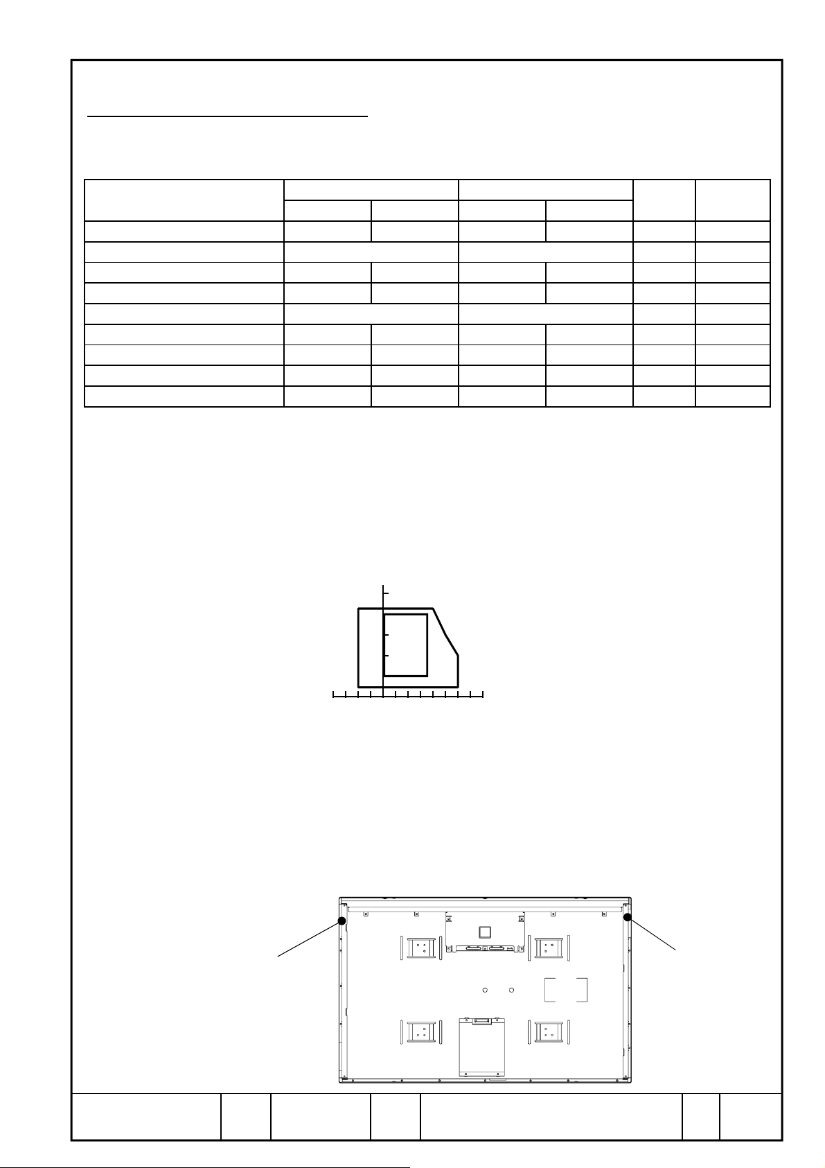
1. ABSOLUTE MAXIMUM RATINGS
1.1 ENVIRONMENT ABSOLUTE MAXIMUM RATINGS
Item Unit Note
Panel surface Temperature 0 50
Operating Storage
Min. Max. Min. Max.
-20 60 °C 1)
Humidity 2) 2) %RH 1)
Vibration - 2.45 (0.25G) - 9.8 (1.0G)
Shock - 14.7 (1.5G) - 294 (30G)
m/s
m/s
2
2
Corrosive Gas Not Acceptable Not Acceptable -
Illumination at LCD Surface - 50,000 - 50,000 lx
TCON Surface Temperature - 85
LED Driver Parts Temperature
-85
Rear frame Temperature -
65 - 65
-85°C 6)
-
85
°C
°C
Notes
1) Temperature and Humidity should be applied to the panel surface of the TFT module and
not to the system installed with the module.
2) Ta ≤ 40°C : Relative humidity should be less than 85%RH max. Dew is prohibited.
Ta > 40°C : Relative humidity should be lower than the moisture of the 85%RH at 40°C .
Relative humidity ( %RH )
100
80
Opera
60
ting
40
range
20
Storage range
3), 5)
4), 5)
7)
8)
20 40 60 80-20-40 0
Environment Temperature ( °C )
3) Frequency of vibration is between 15Hz and 100Hz, except resonance point and z-direction
( panel face top and bottom ).
4) Pulse width of the shock wave pattern is 10ms approximately.
5) The LCD module should be mounted and fixed to a monitor chassis by all 16 screws whose holes
are located two each at top, bottom, right and left side, and remaining 8 pcs at rear side of the module.
6) FPGA-IC
7)MOSFET
8) See below picture.
LED position
LED position
Japan Display Inc.
Date Mar. 26, 2013 Page
Sh.
No.
DPBC10000482 - 1
4-1/2
1.2 ELECTRICAL ABSOLUTE MAXIMUM RATINGS
(1) TFT-LCD Module
Vss = 0 V
Item Symbol Min. Max. Unit Note
Power Supply Voltage V
Input Differential voltage swing V
Input common mode voltage V
Electrostatic Durability
V
V
DD
ID
ICM
ESD0
ESD1
- 13.2 V
100 900 mV 1)
500 1800 mV 1)
±100 V 2),3)
±8 kV 2),4)
Notes 1) It is applied to LVDS specifications.
Positive Channel
Typ 1.25V
VICM VID
Negative Channel
Ground
2) Discharge Coefficient: 200pF-250Ω, Environmental: 25°C-70%RH
3) It is applied to I/F connector pins.
4) It is applied to the surface of a metallic bezel and a LCD panel.
(2) LED driver
Vss = 0 V
Item Symbol Min. Max. Unit Note
Input Voltage Vin - 30.0 V
ON/OFF Control Input Voltage ON/OFF 0 6.0 V
PWM dimming signal Voltage PWM 6.0
0V
Japan Display Inc.
Date Mar. 26, 2013 Page
Sh.
No.
DPBC10000482 - 1
4-2/2
2. INITIAL OPTICAL CHARACTERISTICS
The following optical characteristics are measured under stable conditions. It takes about 30 minutes
to reach stable conditions. The measuring point is the center of display area unless otherwise noted.
The optical characteristics should be measured in a dark room or equivalent environment.
All initial optical characteristic items should be applied when panels have been shipped.
Measuring equipment : CS-1000A or CA-210, EZ-contrast
Ambient Temperature =25±3°C, VDD=12.0V, fV=60Hz, Vin=24V
2.1 SPECIFICATION
Items Condition
Contrast ratio (900) (1100) - -
Contrast ratio at ±85° (50) - - ° 1)
Brightness (550) (650) -
Brightness
uniformity
Color
chromaticity
Variation of color point
by viewing angle (Gray scale = 1023)
Gray scale = 1023
Gray scale = 511 θ = 0
Red
Green
Blue
White
x (0.615) (0.645) (0.675)
y (0.297) (0.327)
x (0.278) (0.308) (0.338)
y (0.590) (0.620) (0.650)
x (0.116) (0.146) (0.176)
y (0.033) (0.063) (0.093)
x (0.269) (0.299) (0.329)
y (0.285) (0.315) (0.345)
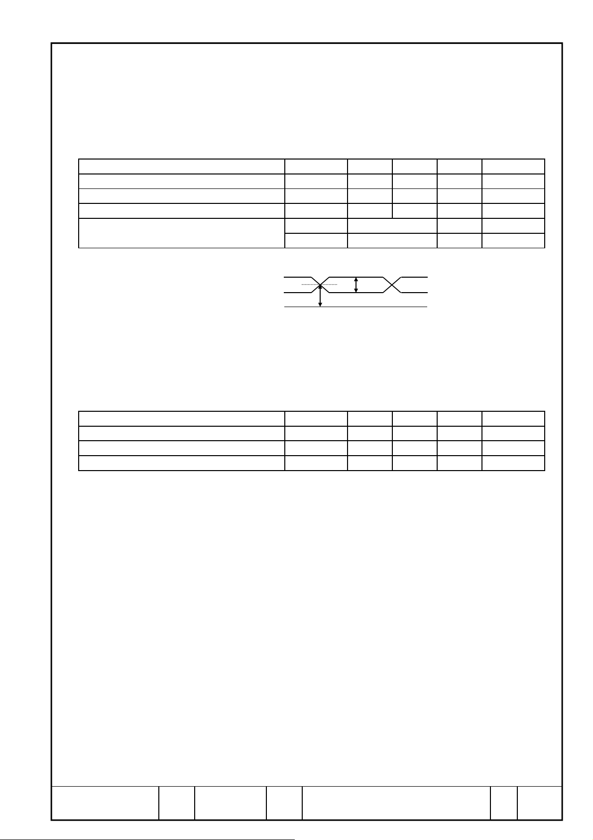
Tr
Response time
Tf θ = 0
Total
γ - (2.2) -
θ = 0
φ = 0, 90, 180, 270
θ = 0
θ = 0
θ = ±80
φ = 0, 90, 180, 270
θ = 0
Min. Typ. Max. Unit Notes
1), 2)
(70) - (65) - -
cd/m
%
2
6)
4)
1)
(0.357)
ΔCIE
- - (0.04)
Δu'v'
5)
- (10) (20) 3)
- (10) (20)
ms
- (20) (40)
-
Japan Display Inc.
Date Mar. 26, 2013 Page
Sh.
No.
DPBC10000482 - 1
5-1/3
 Loading...