

Page 1

TECHNICAL DATA
仕様書パターン2 CAS表紙
Date : Aug 23, 2012
Product Name
(NOTES)
1. This document may, wholly or partially, be subject to change without notice.
2. All rights are reserved ; No one is permitted to reproduce, duplicate or distribute in any form,
the whole or part of this document without Japan Display's prior written consent.
3. No one is permitted to explain nor disclose the contents of this document to third parties without
Japan Display's prior written consent.
4. Japan Display will not be held responsible for any damage to the user that may result from accidents
or any other reasons during operation of the user's unit according to this document, any previous
reports or oral discussions.
5. Circuitry and other examples described herein are meant merely to indicate the characteristics and
performance of Japan Display's products.
Japan Display assumes no responsibility for any intellectual property claims or other problems that
may result from applications based on the examples described herein.
6. No license is granted by implication or otherwise under any patents or other rights of any third
party or Japan Display Inc.
7. LIFE SUPPORT APPLICATIONS : The product covered by this document is not authorized for
use in LIFE SUPPORT SYSTEMS.
TX54D72VC0BAA
Page 2

CONTENTS
DIMENSIONAL OUTLINE
DPBC10000347 - 1
10-1/2 - 10-2/2
7
No. Item Sheet No. Page
-
CONTENTS DPBC10000347 - 1 1-1/1
-
RECORD OF REVISIONS DPBC10000347 - 1 2-1/1
-
DESCRIPTION DPBC10000347 - 1 3-1/1
1
ABSOLUTE MAXIMUM RATINGS DPBC10000347 - 1
2
INITIAL OPTICAL CHARACTERISTICS
3
ELECTRICAL CHARACTERISTICS DPBC10000347 - 1
4
BLOCK DIAGRAM DPBC10000347 - 1 7-1/1
5
INTERFACE PIN ASSIGNMENT DPBC10000347 - 1
6
INTERFACE TIMING DPBC10000347 - 1
7
DIMENSIONAL OUTLINE DPBC10000347 - 1
8
DESIGNATION OF LOT MARK DPBC10000347 - 1
9
COSMETIC SPECIFICATIONS DPBC10000347 - 1
10
PRECAUTION DPBC10000347 - 1
DPBC10000347 - 1
4-1/2 - 4-2/2
5-1/3 - 5-3/3
6-1/1
8-1/5 - 8-5/5
9-1/5 - 9-5/5
10-1/2 - 10-2/2
11-1/1
12-1/3 - 12-3/3
13-1/3 - 13-3/3
Japan Display Inc.
Date Aug. 23, 2012
Sh.
No.
DPBC10000347 - 1
Page 1-1/1
Page 3

RECORD OF REVISIONS
Date Sheet No. Summary
Japan Display Inc.
Date Page
Sh.
No.
DPBC10000347 - 1
2-1/1Aug. 23, 2012
Page 4

DESCRIPTION
Sh.
Note : The LED driver for the backlight unit is integrated within this module.
Product Name : TX54D72VC0BAA
GENERAL SPECIFICATIONS
Effective Display Area : (H)431.616 × (V)323.712 (mm)
Number of Pixels : (H)2,048 × (V)1,536 (pixels)
Aspect ratio : 4 : 3
Pixel Pitch : (H)0.21075 × (V)0.21075 (mm)
Color Pixel Arrangement : R+G+B Vertical Stripe
Display Mode : Transmissive Mode
Normally Black Mode
Frame frequency : 60 Hz
Top Polarizer Type : Anti-glare (Surface hardness: 2H)
Number of Colors :1,073,741,824 colors ( 10bit )
LCM Mode : IPS-Pro
Input Signal : 4-channel LVDS (LVDS = Low Voltage Differential Signaling)
Back Light : Edge Light Type with White LED
External Dimensions : (H)460.6 × (V)359.0 × (t)29.0 typ. (mm)
Weight : 3,200g typ.(3,400g max.)
Japan Display Inc. Date Aug. 23, 2012 DPBC10000347 - 1 Page
No.
3-1/1
Page 5

1. ABSOLUTE MAXIMUM RATINGS
100
Sh.
1.1 ENVIRONMENT ABSOLUTE MAXIMUM RATINGS
Item Unit Note
Panel surface Temperature 0 60
Operating Storage
Min. Max. Min. Max.
-20 60 °C 1)
Humidity 2) 2) %RH 1)
Vibration - 2.45 (0.25G) - 14.7 (1.5G)
Shock
- 14.7 (1.5G) - 294 (30G)
- 14.7 (1.5G) - 490 (50G)
m/s
m/s
m/s
2
2
2
3),5)
4),5)
4),6)
Corrosive Gas Not Acceptable Not Acceptable -
Illumination at LCD Surface - 50,000 - 50,000 lx
TCON Surface Temperature - 85
- 85 °C 7)
Notes
1) Temperature and Humidity should be applied to the panel surface of the TFT module and
not to the system installed with the module.
2) Ta ≤ 40°C : Relative humidity should be less than 85%RH max. Dew is prohibited.
Ta > 40°C : Relative humidity should be lower than the moisture of the 85%RH at 40°C .
Relative humidity ( %RH )
100
80
Opera
60
ting
40
range
20
Storage range
20 40 60 80-20-40 0
Environment Temperature ( °C )
3) Frequency of vibration is between 15Hz and 100Hz, except resonance point and z-direction
( panel face top and bottom ).
4) Pulse width of the shock wave pattern is 10ms approximately.
5) LCD module mounted with chassis by screwed all 4 positions, which 4 positions are
right and left side. (chassis thickness should be 1.5mm max.)
6) LCD module must be mounted with chassis by screwed all 8 positions, which 4 positions are
top and bottom side, other 4positions are on right and left side.
7) FPGA-IC
No.
DPBC10000347 - 1 PageJapan Display Inc. Date Aug. 23, 2012
4-1/2
Page 6

1.2 ELECTRICAL ABSOLUTE MAXIMUM RATINGS
Vss = 0 V
Sh.
(1) TFT-LCD Module
Item Symbol Min. Max. Unit Note
V
V
V
V
V
DD
ID
ICM
ESD0
ESD1
Power Supply Voltage
Input Differential voltage swing
Input common mode voltage
Electrostatic Durability
Notes 1) It is applied to LVDS specifications.
Typ 1.25V
V
ICM
2) Discharge Coefficient: 200pF-250Ω, Environmental: 25°C-70%RH
3) It is applied to I/F connector pins.
4) It is applied to the surface of a metallic bezel and a LCD panel.
(2) LED driver
VSS = 0 V
0 13.2 V
100 900 mV 1)
500 1800 mV 1)
±100 V 2),3)
±8 kV 2),4)
Positive Channel
Negative Channel
V
ID
Ground
Item Symbol Min. Max. Unit Note
Input Voltage
ON/OFF Control Input Voltage ON/OFF 0 5.5 V
Analog dimming signal Voltage VBR 0 3.6 V 1)
PWM dimming signal Voltage PWM 0 5.5 V 1)
Notes 1) These signals can’t input at the same time.
V
IN
0 28.0 V
Japan Display Inc. Date Aug. 23, 2012 DPBC10000347 - 1 Page
No.
4-2/2
Page 7

2. INITIAL OPTICAL CHARACTERISTICS
cd/m
y
0.023
0.053
0.083
Blue
Sh.
The following optical characteristics are measured under stable conditions. It takes about 30 minutes
to reach stable conditions. The measuring point is the center of display area unless otherwise noted.
The optical characteristics should be measured in a dark room or equivalent environment.
Measuring equipment : CS-1000A or CA-210, EZ-contrast
Ambient Temperature =25±3°C, VDD=12.0V, fV=60Hz, Vin=24V
2.1 SPECIFICATION
Item Symbol Condition Min. Typ. Max. Unit Note
Contrast Ratio CR 800 1400 — — 2)
Response Rise ton — 12 22
Time Fall toff — 10 20
Brightness of white Bwh 800 1000 —
Brightness uniformity Buni 70 — — % 4)
Red
Color x 0.274 0.304 0.334
Chromaticity y 0.592 0.622 0.652 — Gray scale
(CIE) x 0.120 0.150 0.180 = 1023
Green
Blue
x θ = 0° 0.626 0.656 0.686
y 1) 0.296 0.326 0.356
ms
2
3)
6)
White
Red
Variation of ∆x θ = +60° — — 0.040 5)
Color Position ∆y
(CIE) ∆x 180°, 270° — — 0.040 Gray scale
Green
Blue
White
x 0.269 0.299 0.329
y 0.285 0.315 0.345
∆x — — 0.040
∆y — — 0.040
φ = 0º, 90º
— — 0.040 —
∆y 1) — — 0.040 = 1023
∆x — — 0.040
∆y — — 0.040
θ = +85°
Contrast Ratio at 85° CR85°
φ = 0º, 90º
50 — — — —
180°, 270° 1)
Japan Display Inc. Date Aug. 23, 2012 DPBC10000347 - 1 Page
No.
5-1/3
Page 8

Notes
φ
CR=
(Luminance at displaying BLACK)
(
Sh.
1) Definition of Viewing Angle ( gray scale = 1023 )
=90°
(12 o'clock)
φ=180
(9 o'clock)
2) Definition of Contrast Ratio (CR)
CR=
X'
LCD Module
(Luminance at displaying WHITE)
Y
θ=0
Z
Z'
θ
eye
Y'
φ=270
(6 o'clock)
φ
φ=0°
X (3 o'clock)
3) Definition of Response Time
Displaying Data Signal BLACK
%
100
90
Optical Response
(Luminance)
10
0
Panel surface temperature = 40°C
4) Definition of Brightness Uniformity
Display pattern is white (1023 level). The brightness uniformity is defined by the following equation.
Brightness at each point is measured and then Buni can be calculated using the maximum and minimum
brightness values.
Buni=
where, Bmax = Maximum brightness.
Bmin = Minimum brightness.
Bmin
Bmax
) ×100
WHITE BLACK
ton
toff
Aug. 23, 2012 DPBC10000347 - 1 PageJapan Display Inc. Date
No.
5-2/3
Page 9

9/10V
5) Variation of color position on CIE is defined as difference between colors for TFT-LCD module.
Sh.
(1)
(2)
(3)
(4)
(7)
1/10V
1/10H
: measuring point
u'=
6) PWM voltage should be 3.0V through 3.3V ( Duty : 100% ).
4x
-2x + 12y +3 -2x + 12y +3
v'=
9y
(5)
(8)
(6)
(9)
9/10H
7) These specifications should be applied with initial performances when it will be shipped.
Japan Display Inc. Date Aug. 23, 2012 DPBC10000347 - 1 Page
No.
5-3/3
Page 10
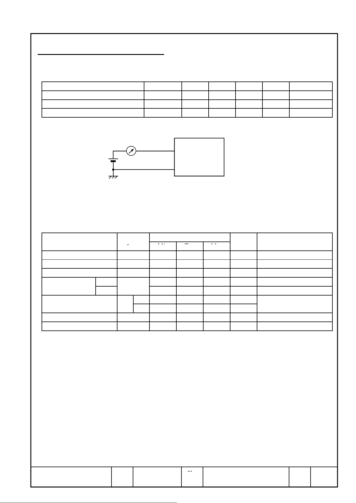
3. ELECTRICAL CHARACTERISTICS
Item
Symbol
Min
Item
Symbol
Unit
Note
Sh.
3.1 TFT-LCD MODULE
Ta=25°C, Vss=0V
Item Symbol Min. Typ. Max. Unit Note
Power Supply Voltage V
Power Supply Current I
Ripple Voltage of Power Supply V
Notes 1) DC current at fv=60.0Hz, fCLK=65MHz, VDD=12.0V and display pattern is a full White (1023).
DD
DD
DDR
11.4 12.0 12.6 V
- 1.0 1.1 A 1),2)
- - 0.15 V
DC Ampere Meter
TFT Module
VDD
VSS
2) A protection fuse is built into this module. Current capacity of the power supply for VDD should be
greater than 5A, so that the fuse can 'blow' if there is a problem with the power supply.
3.2 BACK LIGHT
Value
Unit Note
Typ Max
Input Voltage Vin 21.6 24.0 26.4 V
Input Current Iin - 2.48 2.74 A
Input Power Pin - - 59.1 W
ON/OFF Control ON 2.5 - 5.0 V
Input Voltage OFF 0.0 - 0.8 V
PWM dimming signal
Input Voltage
PWM Duty %
PWM Frequency 1)
ON/OFF
High 3.0 - 5.0 Vdc
PWM
Low 0.0 -
-
5 - 100
0.9
PWMf 140 150 160 Hz
Vdc
Notes 1) PWM Frequency
It could be operate at 100~1000Hz.
However,display specifications
should be applied at 140~160Hz.
2) A protection fuse is built into this
module. Current capacity of the
power supply for Vin should be
greater than 8A, so that the fuse
can 'blow' if there is a problem
with the power supply.
No.
PageJapan Display Inc. Date Aug. 23, 2012 DPBC10000347 - 1
6-1/1
Page 11
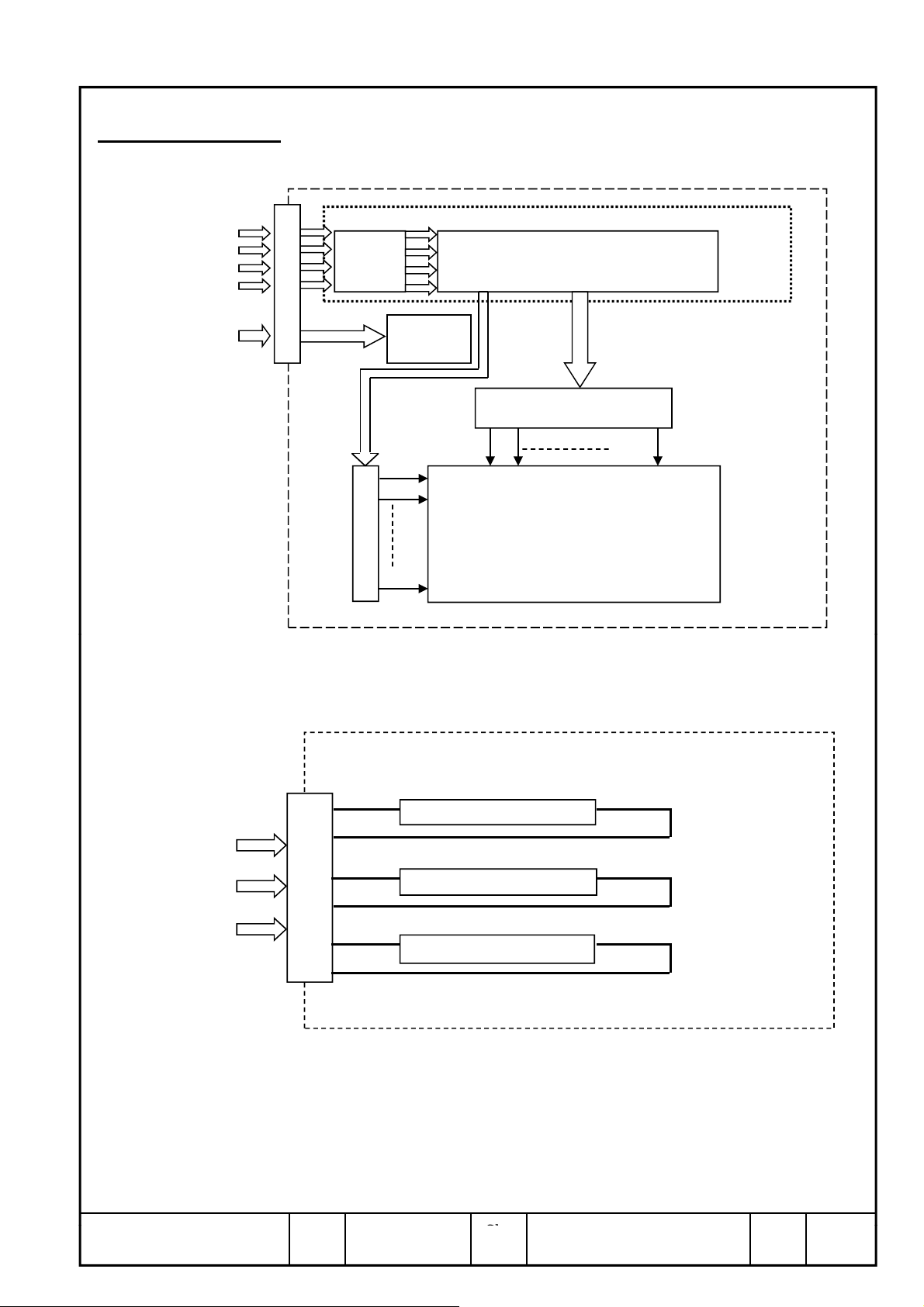
4. BLOCK DIAGRAM
(1) TFT Module
LVDS
Timing
Picture
Control
LVDS
Receiver
Timing
Converter
Tcon
DC power supply
(2) Back light unit
DC/DC
Converter
G1
G2
Gate Driver
G1536
Drain Driver
D1 D2 D2048
TFT-LCD
LED (Series)
DC power supply
ON/OFF Control
LED (Series)
LED driver
Brightness Control
LED (Series)
Japan Display Inc. Date Aug. 23, 2012 DPBC10000347 - 1 Page
Sh.
No.
7-1/1
Page 12
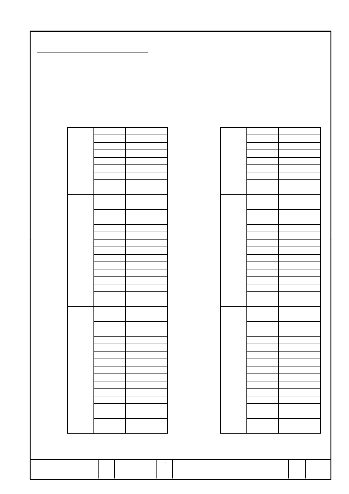
5. INTERFACE PIN ASSIGNMENT
LEFT I/F connector (CN1)
RIGHT I/F connector (CN2)
(CH1, 2)
(CH3, 4)
ARX0p
CRX0p
ARX1p
CRX1p
ARX2p
CRX2p
ACLKp
CCLKp
ARX3p
CRX3p
ARX4p
CRX4p
BRX0p
DRX0p
BRX1p
DRX1p
BRX2p
DRX2p
BCLKp
DCLKp
BRX3p
DRX3p
BRX4p
DRX4p
CH1: ARXn/p
CH3: CRXn/p
CH2: BRXn/p
CH4: DRXn/p
5.1 TFT-LCD MODULE
INPUT CONNECTOR : HIROSE
Plug FX15S-41S-0.5SH (PCB connector side)
FX15S-41P-C (cable side)
Power
Supply
1
2
3
4
5
6 Vss 6 Vss
DD
V
V
DD
DD
V
V
DD
DD
V
Power
Supply
7 Vss 7 Vss
8 Vss 8 Vss
9 Vss 9 Vss
10 ARX0n 10 CRX0n
11
12 ARX1n 12 CRX1n
13
14 Vss 14 Vss
15 ARX2n 15 CRX2n
16
CH1 CH3
17 ACLKn 17 CCLKn
18
19 Vss 19 Vss
20 ARX3n 20 CRX3n
21
22 ARX4n 22 CRX4n
23
24 Vss 24 Vss
25 BRX0n 25 DRX0n
26
27 BRX1n 27 DRX1n
28
29 Vss 29 Vss
30 BRX2n 30 DRX2n
31
32 BCLKn 32 DCLKn
CH2 CH4
33
34 Vss 34 Vss
35 BRX3n 35 DRX3n
36
37 BRX4n 37 DRX4n
38
39 Vss 39 Vss
40 NC 40 NC
41 NC 41 NC
1
2
3
4
5
11
13
16
18
21
23
26
28
31
33
36
38
DD
V
V
DD
DD
V
V
DD
DD
V
Japan Display Inc. Date Page 8-1/5
Aug. 23, 2012
Sh.
No.
DPBC10000347 - 1
Page 13
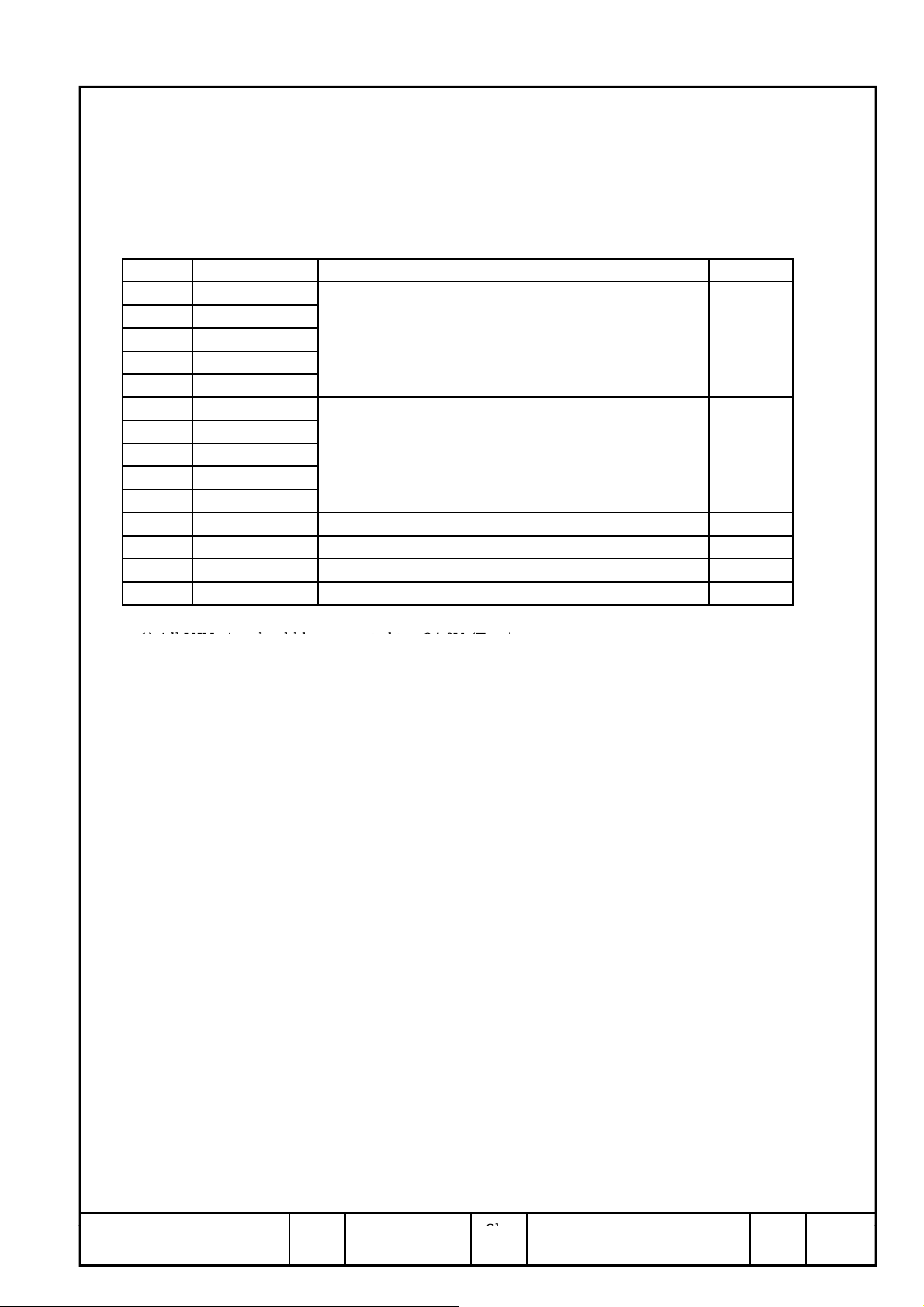
5.2 BACK-LIGHT UNIT
1) All VIN pins should be connected to +24.0V (Typ.).
Sh.
CN3 : JST S14B-PH-SM4-TB (Inverter PCB Connector side)
(Matching connector : JST PHR-14 (Cable side))
Pin No. Symbol
1 V
2 V
3 V
4 V
5 V
IN
IN
IN
IN
IN
Power Supply (typ. 24.0V)
Description Note
6 Vss
7 Vss
8 Vss GND (0V)
9 Vss
10 Vss
11 NC NC
12 ON/OFF High : LED ON, Low : LED OFF
13 NC NC (Open)
14 PWM PWM dimming signal
Notes
1)
2)
3)
2) All VSS pins should be grounded. The metal bezel is internally connected to GND.
3) This pin is connected to internal circuit. It should be open.
Japan Display Inc. Date Aug. 23, 2012 DPBC10000347 - 1 Page
No.
8-2/5
Page 14
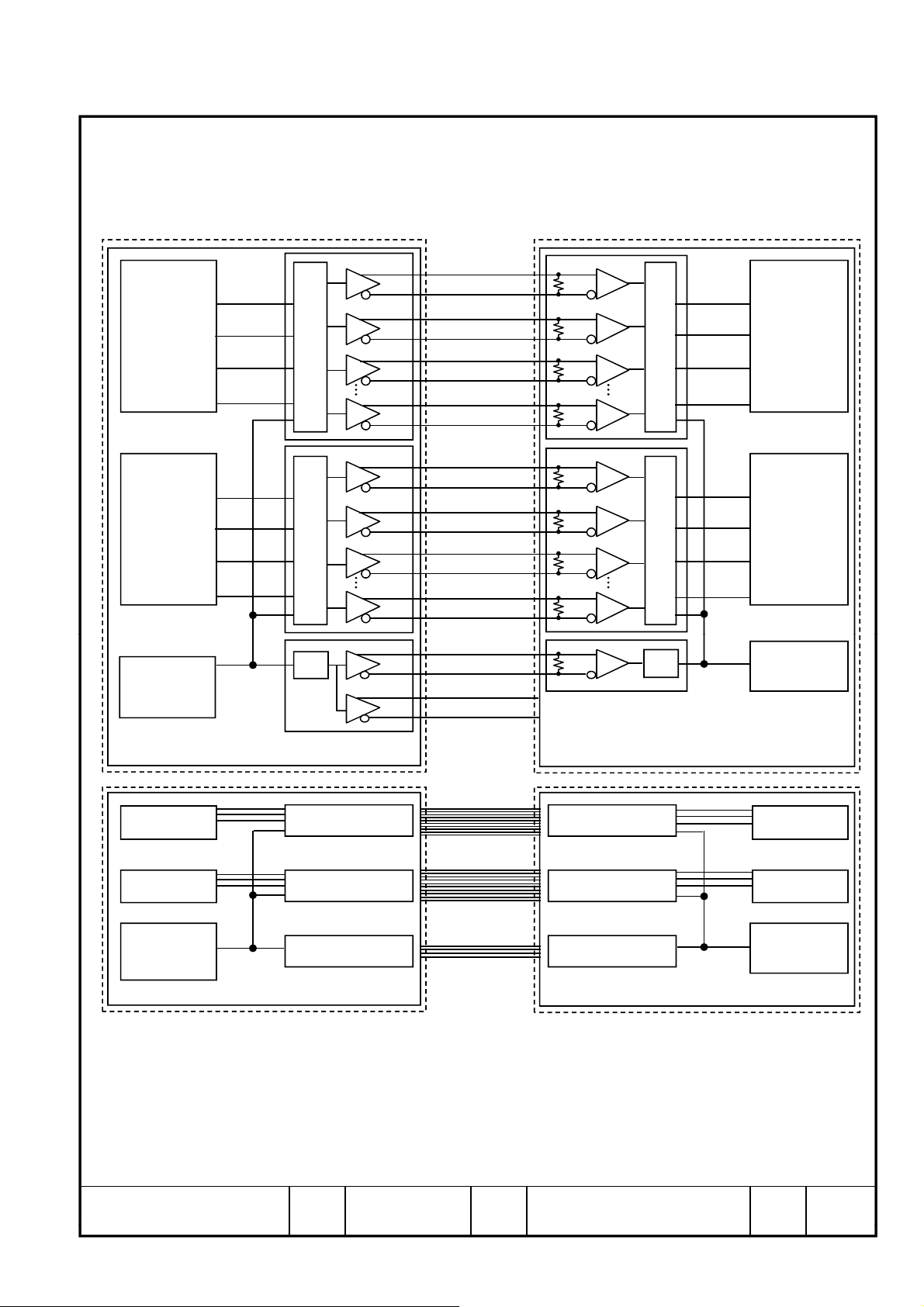
5.3 BLOCK DIAGRAM OF INTERFACE
No.No.
TFT-LCD Module SideGraphic Side
horizontal pixel
(1 - 1023)
R0-R9
G0-G9
B0-B9
DTMG
horizontal pixel
(2 - 1024)
R0-R9
G0-G9
B0-B9
DTMG
Host
Graphics
Controller
1TxIN
ODD
2TxIN
EVEN
CH1
CH2
1Tx 0p
1Tx 0n
1Tx 1p
1Tx 1n
1Tx 2p
1Tx 2n
1Tx 4p
1Tx 4n
2Tx 0p
2Tx 0n
2Tx 1p
2Tx 1n
2Tx 2p
2Tx 2n
2Tx 4p
2Tx 4n
1TCLKp
1TCLKnDCLK
2TCLKp
2TCLKn
ARx 0p
ARx 0n
ARx 1p
ARx 1n
ARx 2p
ARx 2n
ARx 4p
ARx 4n
BRx 0p
BRx 0n
BRx 1p
BRx 1n
BRx 2p
BRx 2n
BRx 4p
BRx 4n
ACLKp
ACLKn
(BCLKp)
(BCLKn)
CH1
100Ω
100Ω
100Ω
100Ω
CH2
100Ω
100Ω
100Ω
100Ω
100Ω
horizontal pixel
ARxOUT
ODD
BRxOUT
EVEN
PLLPLL
(1 - 1023)
R0-R9
G0-G9
B0-B9
DTMG
horizontal pixel
(2 - 1024)
R0-R9
G0-G9
B0-B9
DTMG
DCLK
Converter
horizontal pixel
(1025 - 2047)
horizontal pixel
(1026 - 2048)
DCLK
Host
Graphics
Controller
3TxIN
ODD
4TxIN
EVEN
LVDS Transmitter
CH3
CH4
CTCLK
PLL
DTCLK
LVDS Transmitter
LVDS Receiver
CH3
CH4
LVDS Receiver
CRxOUT
ODD
DRxOUT
EVEN
horizontal pixel
(1025 - 2047)
horizontal pixel
(1026 - 2048)
DCLKPLL
Converter
R0 ~ R9 : Pixel R Data
G0 ~ G9 : Pixel G Data
B0 ~ B9 : Pixel B Data
DTMG : Display timing signal
DCLK : Dot Clock
Notes 1) The host system must have the transmitter in-situ to drive the module.
2) LVDS cable impedance should be 100 ohms per twisted-pair line when used differentially.
Sh.
Japan Display Inc. Date Aug. 23, 2012 DPBC10000347 - 1 Page
Sh.
8-3/5
Page 15
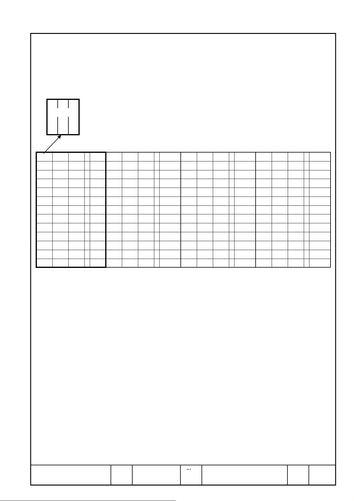
5.4 CORRESPONDENCE BETWEEN INPUT DATA AND DISPLAY IMAGE
Sh.
Display data of adjacent pixel is latched during one cycle of DCLK.
(1,1)
pixel : R0 ~ R9 : R data
G0 ~ G9 : G data
R G B
1,1 3,1 5,1 … 1023,1 2,1 4,1 6,1 … 1024,1 1025,1 1027,1 1029,1 … 2047,1 1026,1 1028,1 1030,1 … 2048,1
1,2 3,2 5,2 … 1023,2 2,2 4,2 6,2 … 1024,2 1025,2 1027,2 1029,2 … 2047,2 1026,2 1028,2 1030,2 … 2048,2
1,3 3,3 5,3 … 1023,3 2,2 4,3 6,3 … 1024,3 1025,3 1027,3 1029,3 … 2047,3 1026,3 1028,3 1030,3 … 2048,3
1,4 3,4 5,4 … 1023,4 2,4 4,4 6,4 … 1024,4 1025,4 1027,4 1029,4 … 2047,4 1026,4 1028,4 1030,4 … 2048,4
: : : : : : : : : : : : : : : : : : : :
: : : : : : : : : : : : : : : : : : : :
: : : : : : : : : : : : : : : : : : : :
: : : : : : : : : : : : : : : : : : : :
: : : : : : : : : : : : : : : : : : : :
: : : : : : : : : : : : : : : : : : : :
: : : : : : : : : : : : : : : : : : : :
: : : : : : : : : : : : : : : : : : : :
1,1536 3,1536 5,1536 … 1023,1536 2,1536 4,1536 6,1536 … 1024,1536 1025,1536 1027,1536 1029,1536 … 2047,1536 1026,1536 1028,1536 1030,1536 … 2048,1536
B0 ~ B9 : B data
CH1 (LEFT_ODD) CH2 (LEFT_EVEN) CH3 (RIGHT_ODD) CH4 (RIGHT_EVEN)
Aug. 23, 2012 DPBC10000347 - 1 PageJapan Display Inc. Date
No.
8-4/5
Page 16
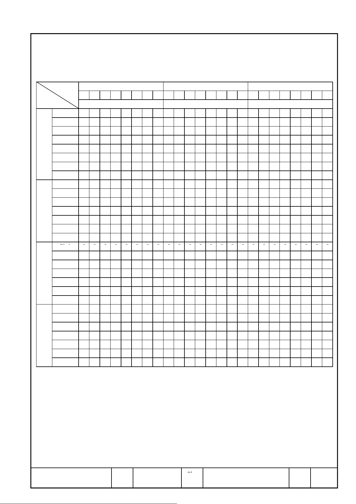
5.5 RELATIONSHIP BETWEEN DISPLAY COLORS AND INPUT SIGNALS
Black000000000000000000000000
Sh.
Input Red Data Green Data Blue Data
R9 R8 R7 ··· R3 R2 R1 R0 G9 G8 G7 ··· G3 G2 G1 G0 B9 B8 B7 ··· B3 B2 B1 B0
Color
Black 0 0 0 0 0 0 0 0 0 0 0 0 0 0 0 0 0 0 0 0 0 0 0 0
Red (1023) 1 1 1 1 1 1 1 1 0 0 0 0 0 0 0 0 0 0 0 0 0 0 0 0
Green (1023)
Basic Blue (1023) 0 0 0 0 0 0 0 0 0 0 0 0 0 0 0 0 1 1 1 1 1 1 1 1
Color Cyan 0 0 0 0 0 0 0 0 1 1 1 1 1 1 1 1 1 1 1 1 1 1 1 1
Magenta 1 1 1 1 1 1 1 1 0 0 0 0 0 0 0 0 1 1 1 1 1 1 1 1
Yellow 1 1 1 1 1 1 1 1 1 1 1 1 1 1 1 1 0 0 0 0 0 0 0 0
White 1 1 1 1 1 1 1 1 1 1 1 1 1 1 1 1 1 1 1 1 1 1 1 1
Black 0 0 0 0 0 0 0 0 0 0 0 0 0 0 0 0 0 0 0 0 0 0 0 0
Red (1) 0 0 0 0 0 0 0 1 0 0 0 0 0 0 0 0 0 0 0 0 0 0 0 0
Red (2) 0 0 0 0 0 0 1 0 0 0 0 0 0 0 0 0 0 0 0 0 0 0 0 0
Red : : : : : : : : : : : : : : : : : : : : : : : : :
Red (1022) 1 1 1 1 1 1 1 0 0 0 0 0 0 0 0 0 0 0 0 0 0 0 0 0
Red (1023) 1 1 1 1 1 1 1 1 0 0 0 0 0 0 0 0 0 0 0 0 0 0 0 0
MSB LSB MSB LSB MSB LSB
0 0 0 0 0 0 0 0 1 1 1 1 1 1 1 1 0 0 0 0 0 0 0 0
: : : : : : : : : : : : : : : : : : : : : : : : :
Green (1) 0 0 0 0 0 0 0 0 0 0 0 0 0 0 0 1 0 0 0 0 0 0 0 0
Green (2) 0 0 0 0 0 0 0 0 0 0 0 0 0 0 1 0 0 0 0 0 0 0 0 0
Green : : : : : : : : : : : : : : : : : : : : : : : : :
: : : : : : : : : : : : : : : : : : : : : : : : :
Green (1022)
Green (1023)
Black 0 0 0 0 0 0 0 0 0 0 0 0 0 0 0 0 0 0 0 0 0 0 0 0
Blue (1) 0 0 0 0 0 0 0 0 0 0 0 0 0 0 0 0 0 0 0 0 0 0 0 1
Blue (2) 0 0 0 0 0 0 0 0 0 0 0 0 0 0 0 0 0 0 0 0 0 0 1 0
Blue : : : : : : : : : : : : : : : : : : : : : : : : :
Blue (1022) 0 0 0 0 0 0 0 0 0 0 0 0 0 0 0 0 1 1 1 1 1 1 1 0
Blue (1023) 0 0 0 0 0 0 0 0 0 0 0 0 0 0 0 0 1 1 1 1 1 1 1 1
0 0 0 0 0 0 0 0 1 1 1 1 1 1 1 0 0 0 0 0 0 0 0 0
0 0 0 0 0 0 0 0 1 1 1 1 1 1 1 1 0 0 0 0 0 0 0 0
: : : : : : : : : : : : : : : : : : : : : : : : :
Notes 1) Definition of gray scale :
Color (n) : Number in parenthesis indicates gray scale level. Larger n corresponds to a brighter level.
2) Data : 1 : High, 0 : Low
Japan Display Inc. Date Aug. 23, 2012 DPBC10000347 - 1 Page
No.
8-5/5
Page 17
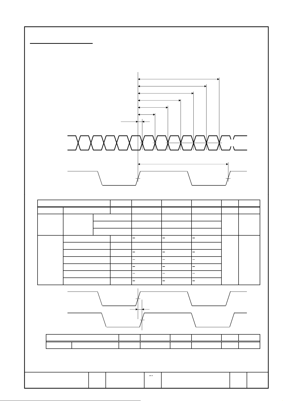
6. INTERFACE TIMING
CLK
CLK
CLK
CLK
CLK
CLK
CLK
CLK
CLK
CLK
CLK
CLK
CLK
Sh.
6.1 LVDS RECEIVER TIMING CHARACTERISTICS
(Regulation with the Input Terminal of the Module)
t
RP0
t
RP1
t
RP2
t
RP3
t
RP4
t
RP5
t
RP6
RinX Rx6
CLKp
Rx5 Rx4
Rx3
Rx2 Rx1 Rx0
RinX=(RinXp)-(RinXn)
t
CLK
Vdiff=0V Vdiff=0V
(X=0,1,2)
Vdiff=0V
Item Symbol Min. Typ. Max.
DCLK MHz
Parameter
1/t
60 65 66
1/tCLK=60MHz -650 0 +650
t
sk
Skew Margin 1/tCLK=65MHz -570 0 +570
1/tCLK=66MHz -550 0 +550
RinX
(X=0,1,2)
Input Data Position0
Input Data Position1
Input Data Position2
Input Data Position3
Input Data Position4
Input Data Position5
Input Data Position6
t
t
t
t
t
t
t
RP0
RP1
RP2
RP3
RP4
RP5
RP6
1
-tsk
7
t
-tsk
0
6
-tsk
7
t
5
-tsk
7
t
4
-tsk
7
t
3
-tsk
7
t
2
-tsk
7
t
1
t
7
CLK
0
6
t
7
CLK
5
t
7
CLK
4
t
7
CLK
3
t
7
CLK
2
t
7
CLK
1
+tsk
7
t
+tsk
0
6
+tsk
7
t
5
+tsk
7
t
4
+tsk
7
t
3
+tsk
7
t
2
+tsk
7
t
Unit Remarks
ps
ns
CH1(2)_CLKp
t
CKP
CH3(4)_CLKp
Item Symbol Min. Typ. Max.
CLKp
Japan Display Inc. Date Aug. 23, 2012 DPBC10000347 - 1 Page
Input CLK Position
t
CKP
-1 0 +1 DCLK
No.
Unit Remarks
9-1/5
Page 18
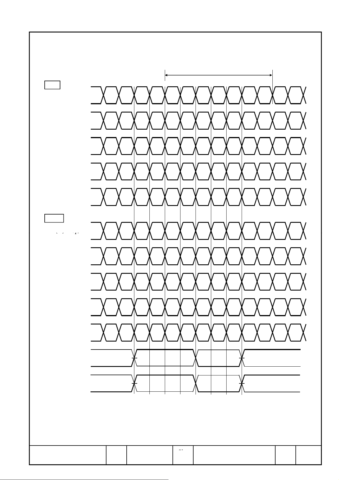
6.2 LVDS MAPPING
B(D)Rx0p/n
B(D)Rx0p/n
R9R8R7R6R5
R4
G4
Input
ODD
1 pixel
Rxm(6) Rxm(5) Rxm(4) Rxm(3)Rxm(2) Rxm(1) Rxm(0)
A(C)Rx0p/n
A(C)Rx1p/n G7 G6 G5
A(C)Rx2p/n
DTMG
A(C)Rx3p/n G3 G2 R3 R2
A(C)Rx4p/n G1 G0 R1 R0B1 B0
R9 R8 R7 R6 R5 R4
G4
B5 B4 G9 G8
-
- -
B3 B2
B9 B8 B7 B6
-
EVEN
B(D)Rx1p/n G7 G6 G5
B5 B4 G9 G8
B(D)Rx2p/n
B(D)Rx3p/n G3 G2 R3 R2
B(D)Rx4p/n G1 G0 R1 R0B1 B0
DTMG
-
-
- -
B3 B2
B9 B8 B7 B6
A(C)RCLKp/n
B(D)RCLKp/n
R0 ~ R9 : Pixel R Data
G0 ~ G9 : Pixel G Data
B0 ~ B9 : Pixel B Data
DTMG : Display timing signal
RCLK : Dot Clock
Japan Display Inc. Date Aug. 23, 2012 DPBC10000347 - 1 Page
Sh.
No.
9-2/5
Page 19
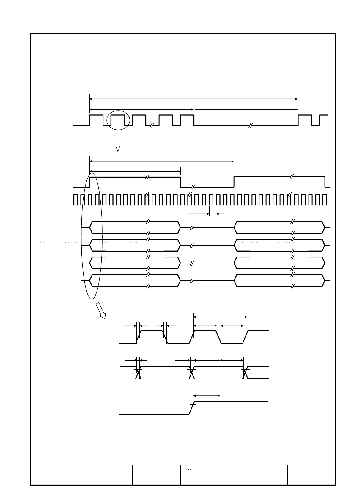
6.3 TIMING CHART
RGB input (CH2)
(n,2) ~ (n,1024)
(n+1,2) ~ (n+1,1024)
Sh.
tV
tVD
tVB
DTMG
tH
tHD
DTMG
DCLK
tCYC
RGB input (CH1) (n,1) ~ (n,1023) (n+1,1) ~ (n+1,1023)
RGB input (CH3) (n,1025) ~ (n,2047) (n+1,1025) ~ (n+1,2047)
RGB input (CH4) (n,1026) ~ (n,2048) (n+1,1026) ~ (n+1,2048)
(n=1,2,3, ~ 1535)
tCYC
tFtR
DCLK
tCH tCL
2.0V
0.8V
tDR tDF tDS tDH
Display Data
2.0V
0.8V
tES
DTMG
Japan Display Inc. Date Aug. 23, 2012 DPBC10000347 - 1 Page
No.
9-3/5
Page 20
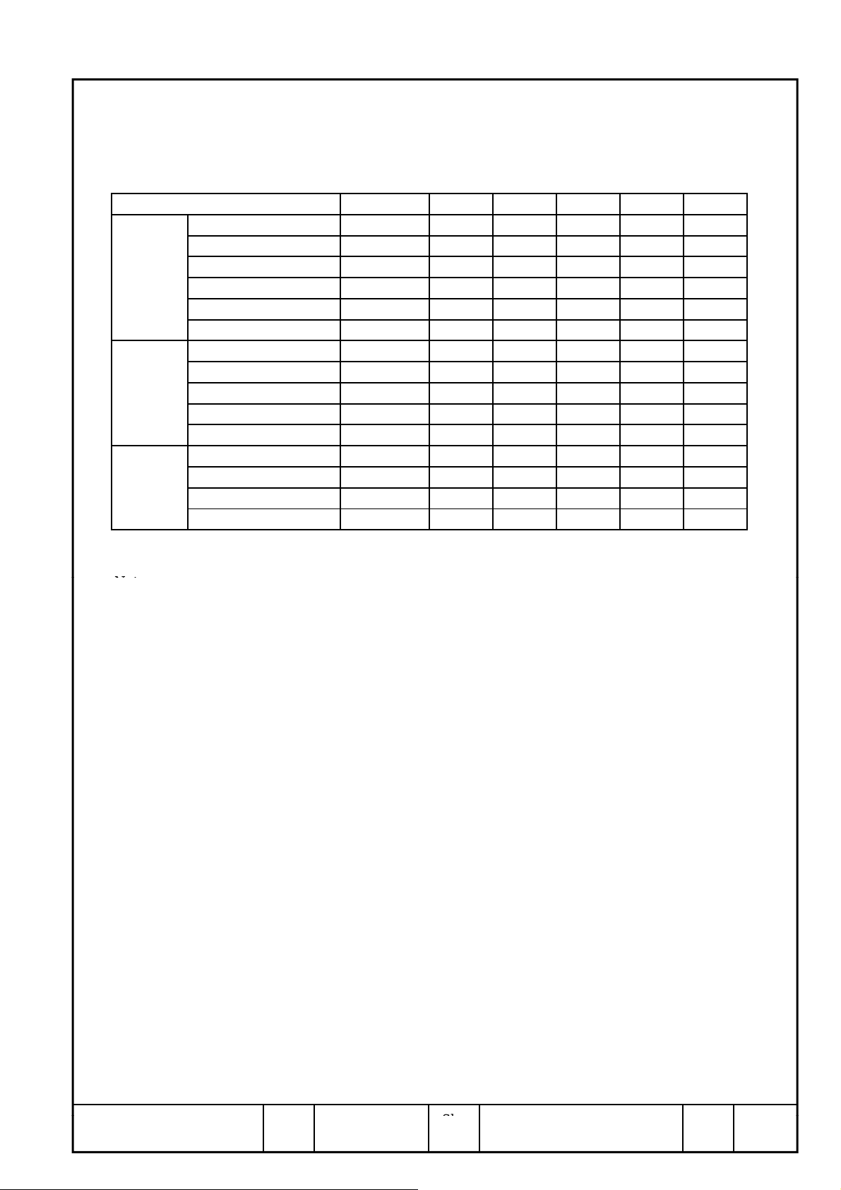
6.4 INTERFACE TIMING SPECIFICATIONS
Sh.
Item Symbol Min. Typ. Max. Unit Note
Frequency 1/tCYC 60 65 66 MHz 1)
Width High tCH 3 - - ns
DCLK
Width Low tCL 3 - - ns
Rise Time tR - - 3 ns
Fall Time tF - - 3 ns
Duty tCH/tCL 45 50 55 %
Period (Hor) tH 640 672 700 tCK
Width Active (Hor) tHD 512 512 512 tCK
DTMG
Period (Ver) tV 1547 1612 1628 tH
Width Active (Ver) tVD 1536 1536 1536 tH
Setup Time tES 4 - - ns
Rise Time tDR - - 3 ns
Display
Data
Fall Time tDF - - 3 ns
Set up Time tDS 3 - - ns
Hold Time tDH 3 - - ns
Note
1) Since DCLK and inverter driving frequency are optimized, please be noted that DCLK should
be set within this spec. Otherwise, optical side effect may happen.
No.
DPBC10000347 - 1 PageJapan Display Inc. Date Aug. 23, 2012
9-4/5
Page 21
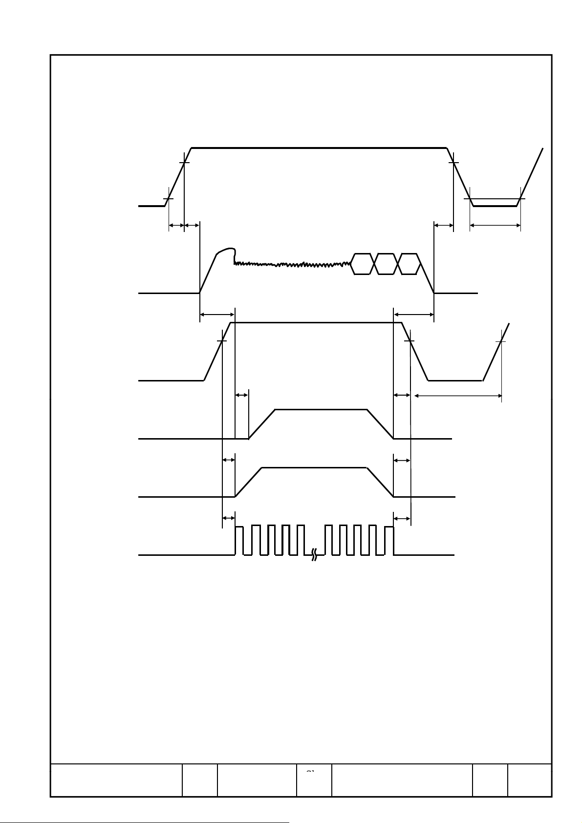
6.5 TIMING BETWEEN INTERFACE SIGNALS AND POWER SUPPLY
Sh.
12V
10V
Power Supply
VDD
1V
0V
TPR
TDR
10V
1V
TINTDF
Interface Signal
(Rx0n, Rx0p,
Rx1n, Rx1p,
Rx2n, Rx2p,
Rx3n, Rx3p,
0V
Rx4n, Rx4p,
CLKn, CLKp)
Back-light
Vin
0V
Back-light
ON/OFF
0V
Back-light
Analog dimming signal 2)
0V
0V
Back-light
PWM dimming signal 2)
TBR
Vin*0.9V
Valid
BLK BLK BLK
TBON
0ms Min.
0ms Min. 0ms Min.
0ms Min. 0ms Min.
1F2F3F
TBF
13V
Vin*0.9V
TINBL
0V
Note
1) Timing of the power supply voltage and input signals should be set using the following specifications.
0ms ≤ TPR ≤ 10ms
10ms ≤ TDR ≤ 50ms
-10ms ≤ TDF ≤ 50ms
TIN ≥ 1000 ms
*Before the end of the Interface Signal, black image is shown for the
last 3 frames. Refer to above Interface Signal Timing.
TBR ≥ 500ms
TBF ≥ 100ms
TBON > 0ms
TINBL ≥ 1000 ms
2) These signals can’t input at the same time.
No.
PageJapan Display Inc. Date Aug. 23, 2012 DPBC10000347 - 1
9-5/5
Page 22
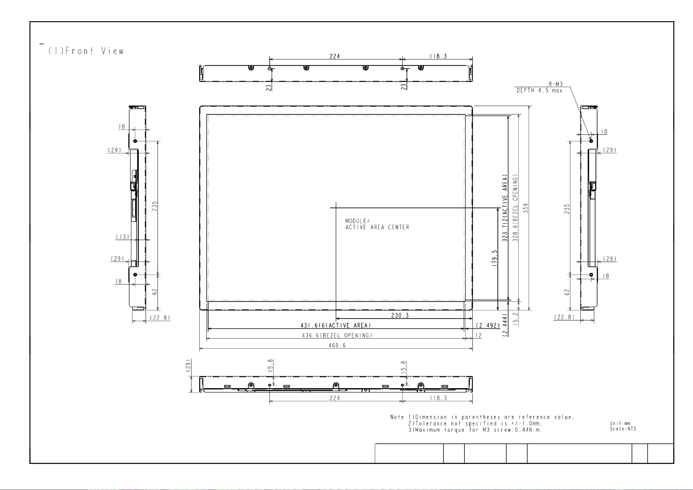
7. DIMENSIONAL OUTLINE
Sh.
Mounting chassis thickness : 1.5mm max.
Japan Display Inc. Date DPBC10000347 - 1 Page 10-1/2
Aug. 23, 2012
Sh.
No.
No.
Page 23
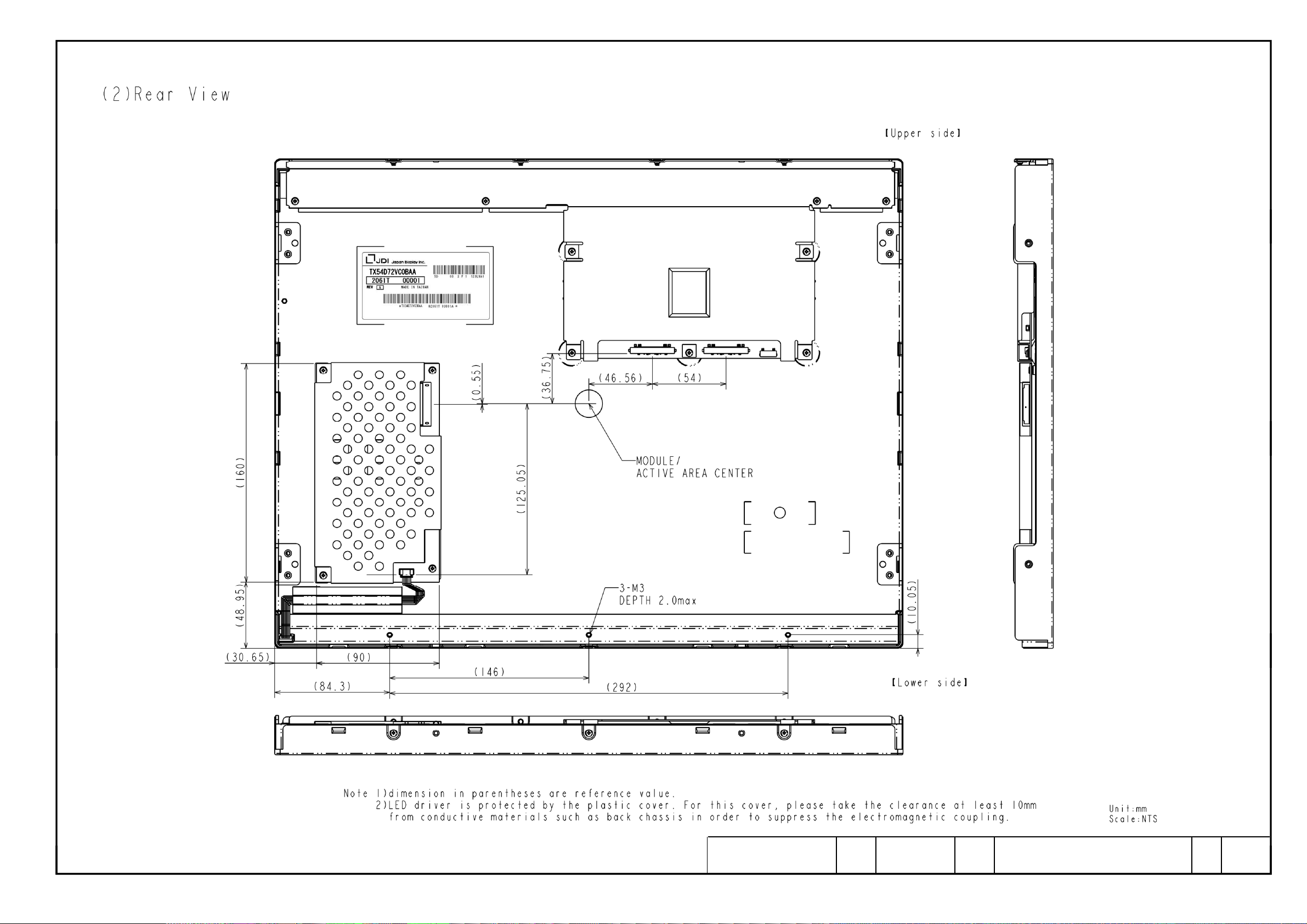
Sh.
Japan Display Inc. Date DPBC10000347 - 1 Page 10-2/2
Aug. 23, 2012
Sh.
No.
No.
Page 24
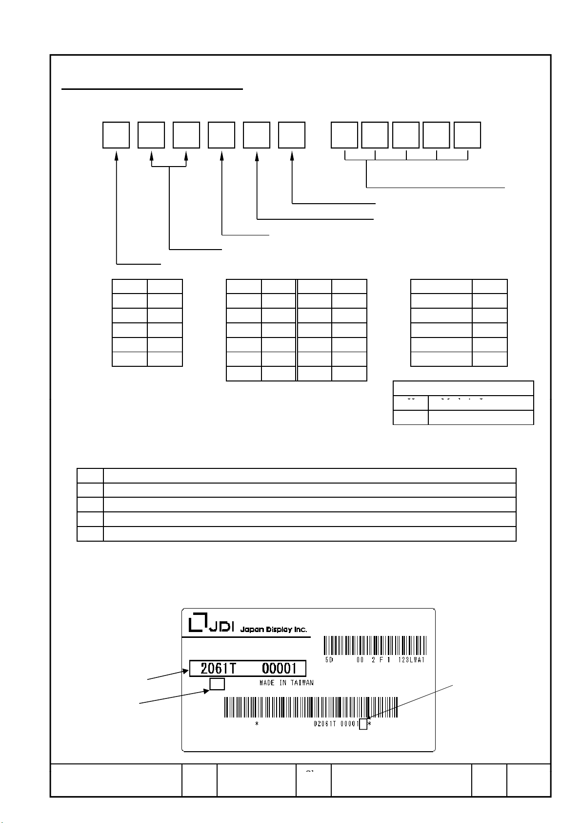
8. DESIGNATION OF LOT MARK
8.1 LOT MARK
Made in Japan
8.3 LOCATION OF LOT MARK
Sh.
5 digits for production number
(00001 ~ 99999)
Optional mark 4)
Production location mark 5)
Week 3)
Month 2)
Year 1)
Notes 1) Year Mark 2) Month Mark Month Mark 3) Week (Day) Mark
2011 1 1 01 7 07 1 ~ 7 1
2012 2 2 02 8 08 8 ~ 14 2
2013 3 3 03 9 09 15 ~ 21 3
2014 4 4 04 10 10 22 ~ 28 4
2015 5 5 05 11 11 29 ~ 31 5
6 06 12 12
4) for Japan Display internal use only. 5) Production management sign
H
T Made in Taiwan
8.2 REVISION (REV.) CONTROL
Revision version is denoted by letter A through Z, except I and O, for Japan Display manufacturing
convenience.
Rev. Note
The Lot mark is printed on a label which is attached to the rear bezel, as shown in 7. External Dimensional.
The style of character can be changed without prior notice.
Lot mark
REV.
TX54D72VC0BAA
TX54D72VC0BAA
TX54D72VC0BAATX54D72VC0BAA
REV
TX54D72VC0BAA
Aug. 23, 2012 DPBC10000347 - 1 PageJapan Display Inc. Date
No.
REV.
11-1/1
Page 25
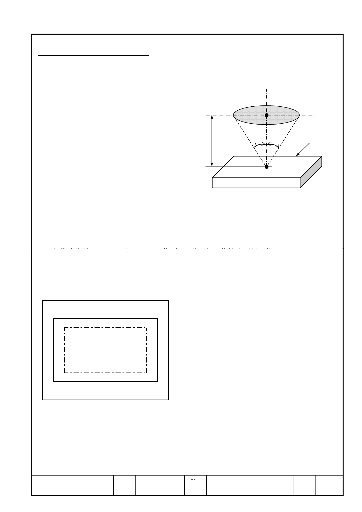
9. COSMETIC SPECIFICATIONS
c)
Back-light
when non-operating inspection, back-light should be off.
Sh.
9.1 CONDITIONS FOR COSMETIC INSPECTION
(1) Viewing zone
Inspection view
a) The figure shows the correspondence
between eyes (of inspector) and
TFT-LCD module.
θ
< 45°
θ
< 5°
b) Inspection should be executed only from
front side and only A-zone.
Cosmetic of B-zone and C-zone are ignore.
(refer to 9.2 DEFINITION OF ZONE)
(2) Environmental
a) Temperature : 25°C
b) Ambient light : sufficient darker condition when operating inspection.
: when non-operating inspection
: when operating inspection
about
300mm
: about 1000 lx and non-directive when non-operating inspection.
:
θ
θ
0
TFT-LCD module
Light
9.2 DEFINITION OF ZONE
A-zone
B-zone
C-zone
•A-zone : Display area (pixel area).
•B-zone : Area between A-zone and C-zone.
•C-zone : Metal bezel area.
(Include I/F connector)
Japan Display Inc. Date Aug. 23, 2012 DPBC10000347 - 1 Page
No.
12-1/3
Page 26
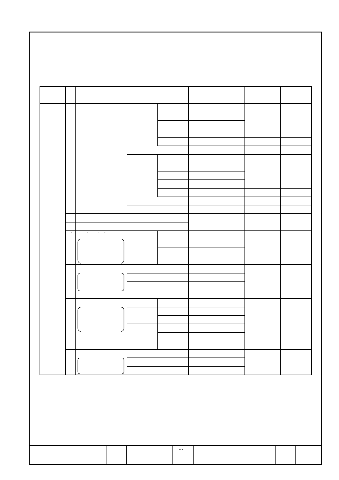
9.3 COSMETIC SPECIFICATIONS
Sh.
When displaying condition is not stable (ex. at turn on or off),
the following specifications are not applied.
Item Unit Note
1-dot 3 pcs 1), 3)
mode 3-dots 0 Units 1), 4)
4-dots 0
Density 2
Total 5 pcs 1)
1-dot 7 pcs 2), 3)
Black 2-dots 3
mode 3-dots 0 Units 2), 4)
4-dots 0
Density 2
Total 7 pcs 2)
Total 10 pcs
L < 1.0 4
W ≤ 0.1
L ≥ 1.0
D ≤ 0.22
D ≤ 0.4
0.4 < D ≤ 0.5
D > 0.5 0
W ≤ 0.02
W ≤ 0.04
W ≤ 0.08
L: Ignore Ignore
L ≤ 40
L > 40 0 pcs 7)
L ≤ 20
L > 20 0
W > 0.08 — 0
D ≤ 0.2
D ≤ 0.6
D > 0.6 0
Operating
inspection
No.
1 Dot Defect Sparkle 2-dots 2
2 Line Defect Serious one is
3 Uneven Brightness not allowed.
Stain Inclusion
4
Line shape
W: width (mm)
L: length (mm)
Stain Inclusion
5
Dot shape
D: ave. dia. (mm)
Scratch on polarizer
6
Line shape
W: width (mm)
L: length (mm)
Scratch on polarizer
7
Dot shape
D: ave. dia. (mm)
Max. acceptable number
A-zone
0
Ignore
5 pcs 6)
4
10
10
Ignore
10 pcs 7)
pcs/φ20mm
pcs/φ20mm
— —
pcs 6)
1), 5)
2), 5)
Japan Display Inc. Date Aug. 23, 2012 DPBC10000347 - 1 Page
No.
12-2/3
Page 27
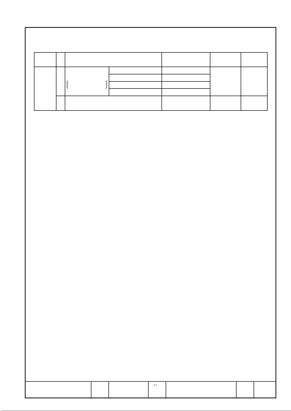
Max. acceptable number
Sh.
A-zone
Ignore
non-
operating
inspection
No. Item Unit Note
Bubbles, peeling
8
in polarizer
D: ave. dia. (mm)
D ≤ 0.3
D ≤ 0.5
D ≤ 1.0
D > 1.0 0
9
Wrinkles on polarizer
Serious one is
not allowed.
Notes 1) Sparkle mode : Brightness of dot is more than 30% at black. (visible to eye)
2)
Black mode: Brightness of dot is less than 70% at white. (visible to eye)
3)
1 dot: Defect dot is isolated, not attached to other defect dot.
4)
N dots: N defect dots are consecutive. (N means the number of defects dots)
5)
Density: Number of defect dots inside 20mm φ.
6)
Those stains which can be wiped out easily are acceptable.
7)
Polarizer area inside of B-zone is not applied.
10 pcs 7)
5
— —
Japan Display Inc. Date Aug. 23, 2012 DPBC10000347 - 1 Page
No.
12-3/3
Page 28
10. PRECAUTION
TFT module
Sh.
Please pay close attention to the following precautions whilst using, handling and mounting the TFT module.
10.1 PRECAUTION FOR HANDLING AND MOUNTING
(1) Applying excessive force to any part of the module may result in partial deformation of the frame or
mould, which could result in permanent damage to the display.
(2) The module should be held gently and firmly using both hands. In order to avoid internal damage,
never hold the module by just one hand. Also never drop or hit the module.
(3) The module should be installed using the mounting holes of the module. In case of using side mounting
hole, chassis thickness should be 1.5mm max.
(4) Uneven force such as twisted stress should not be applied directly to the module once it is mounted
within the cover case. The cover case must have sufficient strength such that any external forces are not
transmitted directly to the module.
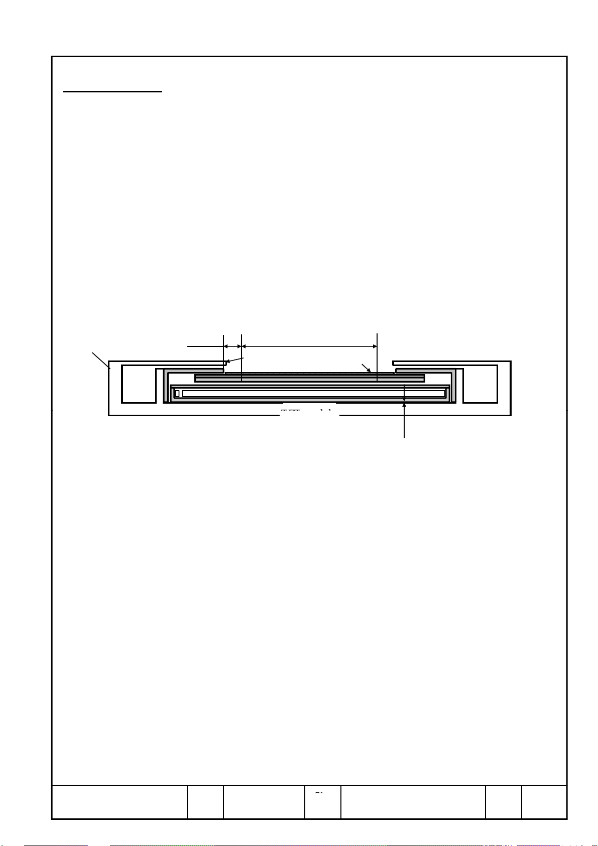
(5) It is recommended that you maintain a gap between the display module and the rear chassis so as to avoid
any mechanical stress being passed to the module.
Cover case
B-zone
Effective display area
Edge of
cover case
Polarizer
Fig.1 Cross sectional view of a monitor set
(6) The edge of the cover case should be positioned with more than a 1mm overlap from the edge of
the module's upper frame.
(7) A transparent protective plate should be added to the front of the display in order to protect both the
polarizer and TFT cell. The transparent protective plate should have sufficient strength such that the
plate can not be deformed, due to external forces, and touch the module.
(8) Materials containing acetic acid and chlorine should not be used for the cover case nor for other parts
which are positioned in close proximity to the module. This is because the Acetic acid will attack
the polarizer, whilst the chlorine will attack the electric circuits by way of electro-chemical reaction.
(9) The front polarizer on the TFT cell should be handled carefully, due to its softness, and must not be
touched, pushed or rubbed with glass, tweezers or anything harder than an HB pencil lead.
The surface of the polarizer should not be touched nor rubbed with bare hands, greasy or dusty clothes.
(10) If the surface of the polarizer becomes dirty it should be gently wiped using an absorbent cotton
(Traysee CC clean cloth), chamois or other soft material, slightly dampened with petroleum benzene.
IPA (isopropyl alcohol) is recommended to clean away the traces of adhesive which is used to attach
the front/rear polarizers to the TFT cell. Other cleaning chemicals such as acetone, toluene and alcohol
should not be used to clean adhesives because they cause chemical damage to the polarizer.
(11) Saliva or water drops should be immediately wiped off. Otherwise, the affected portion of the polarizer
may become deformed and its color may fade.
(12) The module should not be opened or modified, under any circumstances, as this may cause it to
malfunction.
above precaution (5)
Japan Display Inc. Date Aug. 23, 2012 DPBC10000347 - 1 Page
No.
13-1/3
Page 29
(13) The metallic bezel of the module should not be handled with bare hand or dirty gloves. Otherwise,
(8) Connecting or disconnecting the I/F cables, whilst the power and data signals are present, could result in
Sh.
the color of the metallic frame may become dirty during its storage. It is recommended to use clean
soft gloves and clean finger stalls whilst the module is handled during incoming inspection and
production assembly processes.
(14) Please pay attention to the packing and handling not to apply strong Z axis vibration. Because during
our vibration test, of course we didn't have any functional failure, but we observed very tiny bright dots
(within spec though) at Z axis direction.
10.2 PRECAUTION TO OPERATION
(1) Spike noise could result in the mis-operation of this module. The level of spike noise should be as follows:
-200mV ≤ over- and under- shoot of VDD ≤ +200mV
VDD including over- and under- shoot should not exceed the absolute maximum ratings.
(2) Optical response times, luminance and chromaticity depend on the temperature of the TFT module.
(3) Sudden temperature changes may cause dew on and/or in the module. Dew can cause damage to the
polarizer and/or electrical contacting areas of the module. Dew causes fading of the image quality.
(4) Using screen saver is recommended that it avoids any potential of sticking image.
(5) This module has high frequency circuits. Sufficient suppression to electromagnetic interference should
be done by the system manufacturers. Grounding and shielding methods may be effective to minimize
such interference.
(6) Noise may be heard when the back-light is operated. If necessary, sufficient suppression should be
done by the system manufacturers.
(7) The module should not be connected or disconnected whilst the main system is operating.
permanent damage to the module. The I/F connectors should only be connected and disconnected after the
power supply and data signal have been turned off.
(9) The ambient temperature near the operated module should be satisfied with the absolute maximum ratings.
Unless it meets the specifications, sufficient cooling system should be adopted to system.
10.3 ELECTROSTATIC DISCHARGE CONTROL
(1) This module consists of a TFT cell and electronic circuits with CMOS-ICs, which are very susceptible to
electrostatic discharge. Persons who are handling the module should be grounded through adequate
methods such as a wrist band. I/F connector pins should not be touched directly with bare hands.
(2) The polarizer protective film should be removed slowly so as to avoid an excessive build-up of
electrostatic charge.
10.4 PRECAUTION TO STRONG LIGHT EXPOSURE
(1) The module should not be exposed to strong light. Otherwise, characteristics of the polarizer and
color filter, may be degraded.
10.5 PRECAUTION TO STORAGE
When modules are stored, for long period's of time, the following precautions should be taken:
(1) Modules should be stored in a dark place. It is prohibited to apply direct sunlight or fluorescent light
during storage. Modules should be stored between 0 to 35°C at normal humidity (60%RH or less).
(2) The surface of the polarizer should not come into direct contact with other objects.
It is recommended that modules should be stored in the original Japan Display shipping box.
Japan Display Inc. Date Aug. 23, 2012 DPBC10000347 - 1 Page
No.
13-2/3
Page 30
10.6 PRECAUTION TO HANDLING PROTECTION FILM
Sh.
(1) The protective film for polarizers should be pealed off slowly and carefully by people who are
electrically grounded with adequate methods such as wrist bands. Also ionized air should be blown
over the module during the peeling process.
Dust on the polarizer should be blown off gently using an ionized nitrogen gun.
(2) The protective film should be peeled off carefully to avoid it rubbing on the polarizer. If the film rubs
together with the polarizer it is possible that a small amount of adhesive may remain on the polarizer.
(3) The module with protective film should be stored under the conditions explained in 9.5 (1). However ,
in case's where the storage time is excessive, some adhesive may remain on the polarizer even after
the protective film has been removed. In the case where a module is stored at higher temperatures
and/or higher humidity, adhesive may remain on the polarizer. Any remaining adhesive may cause
non-uniformity of the displayed image.
10.7 SAFETY
(1) Since the TFT cell is made of glass, handling of any broken module's should be carried out with
the utmost care so as to avoid any injury. Hands which have come into direct contact with
liquid crystal material should be washed immediately and thoroughly.
(2) The module should not be taken apart during operation so that back-light drives by high voltage.
10.8 USE RESTRICTIONS AND LIMITATIONS
(1) In no event shall Japan Display be liable for any incidental, indirect or consequential damages in
connection with the installation or use of this product, even if informed of the possibility there of
in advance. These limitations apply to all causes action in aggregate, including without limitation breach
of contract, breach of warranty, negligence, strict liability, misrepresentation and other torts.
(2) This product is not authorized for military applications or other applications which pose a significant risk
of personal injury.
Japan Display Inc. Date Aug. 23, 2012 DPBC10000347 - 1 Page
No.
13-3/3
 Loading...