

JDI TX48D02VM0BAA Specification
1
ABSO
GS
C
7
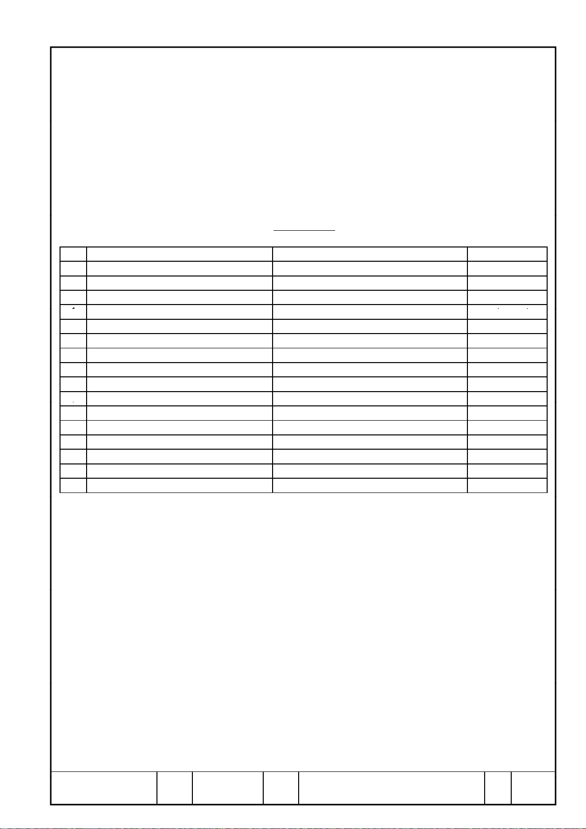
CONTENTS
No. Item Sheet No. Page
CONTENTS 3284PS 2601 - TX48D02VM0BAA - 2C 1-1/1
-
RECORD OF REVISION 3284PS 2602 - TX48D02VM0BAA - 2C 2-1/1
-
DESCRIPTION 3284PS 2603 - TX48D02VM0BAA - 2C 3-1/1
-
LUTE MAXIMUM RATIN
INITIAL OPTICAL CHARACTERISTICS 3284PS 2605 - TX48D02VM0BAA - 2C 5-1/2 - 5-2/2
2
ELECTRICAL CHARACTERISTICS 3284PS 2606 - TX48D02VM0BAA - 2C 6-1/2 - 6-2/2
3
BLOCK DIAGRAM 3284PS 2607 - TX48D02VM0BAA - 2C 7-1/1
4
INTERFACE PIN ASSIGNMENT 3284PS 2608 - TX48D02VM0BAA - 2C 8-1/6 - 8-6/6
5
INTERFACE TIMING 3284PS 2609 - TX48D02VM0BAA - 2C 9-1/3 - 9-3/3
6
DIMENSIONAL OUTLINE 3284PS 2610 - TX48D02VM0BAA - 2C 10-1/2 - 10-2/2
DESIGNATION OF LOT MARK 3284PS 2611 - TX48D02VM0BAA - 2C 11-1/1
8
COSMETIC SPECIFICATIONS 3284PS 2612 - TX48D02VM0BAA - 2C 12-1/3 - 12-3/3
9
PRECAUTIONS 3284PS 2613 - TX48D02VM0BAA - 2C 13-1/3 - 13-3/3
10
3284PS 2604 - TX48D02VM0BAA - 2
4-1/2 - 4-2/2
Japan Display Inc.
Date Jan. 07, 2013 Page
Sh.
No.
3284PS 2601 -
TX48D02VM0BAA - 2C
1-1/1

RECORD OF REVISION
Date Sheet No. Page
Jan. 07, 2013
3284PS 2603-TX48D02VM0BAA-1C
3284PS 2603-TX48D02VM0BAA-2C
3284PS 2604-TX48D02VM0BAA-1C
3284PS 2604-TX48D02VM0BAA-2C
3284PS 2604-TX48D02VM0BAA-1C
3284PS 2604-TX48D02VM0BAA-2C
3284PS 2605-TX48D02VM0BAA-1C
3284PS 2605-TX48D02VM0BAA-2C
3284PS 2606-TX48D02VM0BAA-1C
3284PS 2606-TX48D02VM0BAA-2C
3284PS 2608-TX48D02VM0BAA-1C
3284PS 2608-TX48D02VM0BAA-2C
3284PS 2608-TX48D02VM0BAA-1C
3284PS 2608-TX48D02VM0BAA-2C
3284PS 2608-TX48D02VM0BAA-1C
3284PS 2608-TX48D02VM0BAA-2C
3284PS 2611-TX48D02VM0BAA-1C
3284PS 2611-TX48D02VM0BAA-2C
3-1/1
4-1/2
4-2/2
5-1/2
6-2/2
8-3/6
10-1/2
10-2/2
11-1/1
Summary
Changed DESCRIPTION
The following specifications are applied to the
following IPS-Pro module.
↓
This specification is applied to the following
IPS-Pro module.
1.1 ELECRTICAL ABSOLUTE MAXIMUM RATING
Added an illustration to Notes 2)
Added Page 4-2/2,and Item 1.2 is moved from Page
4-1/2 to Page 4-2/2.
2. INITIAL OPTICAL CHARACTERISTICS
Changed Brightness of white
Min. 280 → 250, Typ. 350 → 300
Changed Variation of Color Position
Max. volue : 0.040 → 0.050
3.2 BACK LIGHT
Added 6) to the note column of the Input Current.
Changed Note 6)
A protection fuse is built into this module.
→A protection fuse is built in this module.
BLOCK DIAGRAM OF INTERFACE
Revised the contents.
7.DIMENSIONAL OUTLINE
Changed Note 2)
Tolerance not specified is ±1㎜.
→Tolerance unspecified is ±1㎜.
7.DIMENSIONAL OUTLINE
Changed Note 2)
Tolerance not specified is ±1㎜.
→Tolerance unspecified is ±1㎜.
8.2 REVISION(REV.) CONTROL
Added Rev.D
Japan Display Inc.
Date Page
Sh.
No.
3284PS 2602 -
TX48D02VM0BAA - 2C
2-1/1Jan. 07, 2013
DESCRIPTION
y
y
This specification is applied to the following IPS-Pro module.
Note :The LED driver for backlight unit is built in this module.
Product Name : TX48D02VM0BAA
Effective Display Area :
Number of Pixels :
Pixel Pitch :
Color Pixel Arrangement :
Display Mode :
Top Polarizer Type
Number of Colors
Viewing Angle Range
Input Signal :
H409.50 × V255.9375 [mm]
H1,680 × V1,050 [pixels]
H0.24375 × V0.24375 [mm]
R+G+B Vertical Stripe
Transmissive Mode
Normall
IPS-Pro
: Anti-glare (Hardness: 2H)
: 16,777,216 colors
: Super Wide Version
2-channel LVDS (LVDS: Low Voltage Differential Signaling)
Black Mode
Back Light : Edge Light Type with White LED
External Dimensions : H444 × V300 × t24.0 [mm]
Weight : Typ. 1,900g
Japan Display Inc.
Date Jan. 07, 2013 Page
Sh.
No.
3284PS 2603 -
TX48D02VM0BAA - 2C
3-1/1
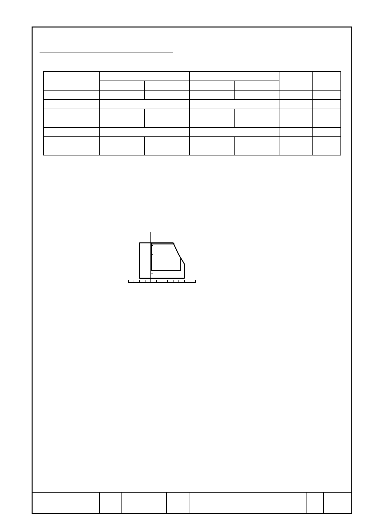
1. ABSOLUTE MAXIMUM RATINGS
60
d
Operating
1.1 ELECTRICAL ABSOLUTE MAXIMUM RATINGS
Item Unit Note
Temperature 0 55 -20 60 °C 1)
Humidity 2) 2) %RH 1)
Vibration — (0.5G) — (1.0G) 3)
Shock — (3G) — (30G) 4)
Corrosive Gas Not Acceptable Not Acceptable — —
Illumination at
LCD Surface
Notes 1) Temperature and Humidity should be applied to the center glass surface of a IPS-Pro module,
not to the system installed with a module.
The temperature at the center of rear surface should be less than 60°C on the condition of operating.
Function of module is guaranteed in above operating temperature range, but optical characteristics
is specified for only 25°C operating condition.
2) Ta ≤ 40°C ……… Relative humidity should be less than 85%RH max. Dew is prohibited.
Ta > 40°C ……… Relative humidity should be lower than the moisture of the 85%RH at 40°C.
Operating Storage
Min. Max. Min. Max.
4.9 9.8
29.4 294
— 50,000 — 50,000 lx
m/s
2
—
100
80
ity ( %RH )
40
20
Storage range
Relative humi
20 40 60 80-20-40 0
range
Environment Temperature ( °C )
3) Frequency of the vibration is between 15Hz and 100Hz. (Except the resonance point)
4) Pulse width of the shock is 10 ms.
Japan Display Inc.
Date Jan. 07, 2013 Page
Sh.
No.
3284PS 2604 -
TX48D02VM0BAA - 2C
4-1/2
1.2 ELECTRICAL ABSOLUTE MAXIMUM RATINGS
(1) TFT Module
Item Symbol Min. Max. Unit Note
V
V
V
V
ESD0
ESD1
DD
I
Power Supply Voltage
Input Voltage for logic
Electrostatic Durability
Notes 1) It is applied to pixel data signal and clock signal.
2) Discharge Coefficient: 200pF-250Ω, Environmental: 25°C-70%RH
3) It is applied to I/F connector pins.
4) It is applied to the surface of a metallic bezel and a LCD panel.
0 13.5 V —
-0.3 3.6 V 1)
Vss=0V
±100 V 2), 3)
±8 kV 2), 4)
(2) Back Light
Item Symbol Min. Max. Unit Note
Input Voltage
ON/OFF Control Input Voltage ON/OFF 0 5.5 V
Analog Dimming Signal Voltage
PWM Dimming Signal Voltage PWM 0 5.5 V 1)
Notes 1) These signals can’t input at the same time.
VSS=0V
V
IN
V
BC
- 16.0 V
05.5V 1)
Japan Display Inc.
Date Jan. 07, 2013 Page
Sh.
No.
3284PS 2604 -
TX48D02VM0BAA - 2C
4-2/2

2. INITIAL OPTICAL CHARACTERISTICS
Whi
The following optical characteristics are measured when the LCD is set alone (apart from driving
circuits and monitor cabinets) and under stable conditions. It takes about 30 minutes to reach stable
conditions. The measuring point is the center of display area unless otherwise noted.
The optical characteristics should be measured in a dark room or equivalent state.
Measuring equipment:KONICA MINOLTA: CS-2000, or equevalent
Ambient Temperature = 25±3°C, V
and V
=3.3V or PWM=100%(PWMf=150Hz)
BC
Item Symbol Condition Min. Typ. Max. Unit Note
Contrast Ratio CR 600 1000 — — 2)
Response Rise ton — 11 19
Time Fall toff — 10 18
Brightness of white Bwh 250 300 —
Brightness uniformity Buni 70 — — % 4)
x θ = 0° 0.618 0.648 0.678
y 1) 0.299 0.329 0.359
x 0.284 0.314 0.344
y 0.584 0.614 0.644 —
x 0.119 0.149 0.179
y 0.028 0.058 0.088
x 0.283 0.313 0.343
y 0.299 0.329 0.359
∆x — — 0.050
∆y — — 0.050
∆x θ = +50° — — 0.050
∆y
∆x 180°, 270° — — 0.050
∆y 1) — — 0.050
∆x — — 0.050
∆y — — 0.050
Color
Chromaticity
(CIE)
Variation of
Color Position
(CIE)
Red
Green
Blue
te
Red
Green
Blue
White
Contrast Ratio at 85° CR85°
=12.0V, fV=60Hz,VIN=12.0V
DD
φ = 0º, 90º
— — 0.050 —
θ = +85°
φ = 0º, 90º
10——— —
180°, 270° 1)
ms 3)
2
cd/m
—
Gray scale
= 255
5)
Gray scale
= 255
Japan Display Inc.
Date Jan. 07, 2013 Page
Sh.
No.
3284PS 2605 -
TX48D02VM0BAA - 2C
5-1/2
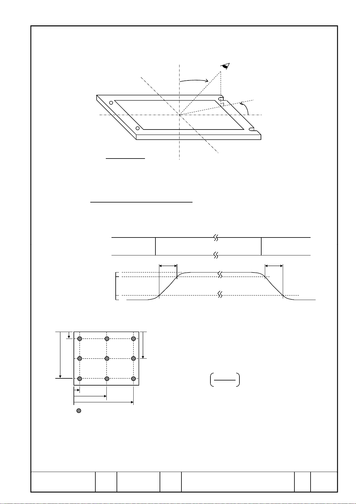
Notes 1) Definition of Viewing Angle
k
φ=90°
(12 o'clock)
θ=0°
Z
Y
θ
eye
φ=180°
(9 o'clock)
TFT Module
2) Definition of Contrast Ratio (CR)
CR =
3) Definition of Response Time
Displaying
Data Signal
Optical
Response
( Luminance)
(Luminance at displaying WHITE)
(Luminance at displaying BLACK)
Black
%
100
90
10
0
ton
Z'
White
φ=270°
Y'
(6 o'clock)
φ
XX'
(3 o'clock)
Blac
toff
φ=0°
4) Definition of Brightness Uniformity
10%
90%
5) Variation of color position on CIE is defined as difference between colors at θ = 0° and
(1)
(4) (5) (6)
(7) (8) (9)
10%
at θ = 50° & φ = 0°, 90°,180°, 270°.
Japan Display Inc.
(3)
(2)
50%
: measuring points
Date Jan. 07, 2013
90%
50%
Display pattern is white (255 level). The brightness
uniformity is defined as the following equation.
Brightness at each point is measured, and average,
maximum and minimum brightness is calculated.
Bmin
Bmax
Bmin = Minimum brightness
TX48D02VM0BAA - 2C
Sh.
No.
Buni = × 100
where, Bmax = Maximum brightness
3284PS 2605 -
Page 5-2/2

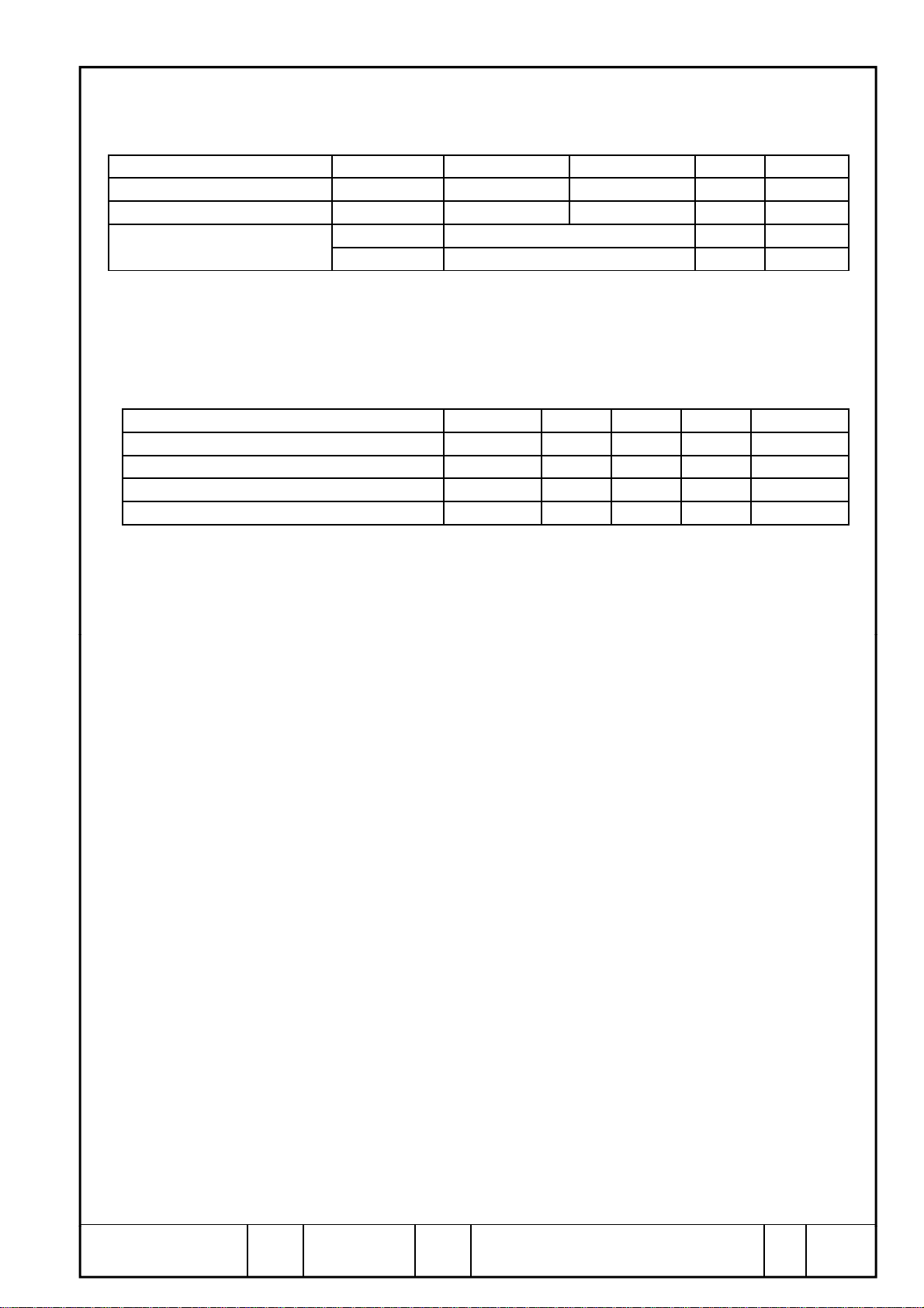
3. ELECTRICAL CHARACTERISTICS
)
pp
3.1 TFT-LCD MODULE
Item Symbol Min. Typ. Max. Unit Note
Power Supply Voltage
Power Supply Current
Vsync Frequency
Hsync Frequency
DCLK Frequency
* The LCD panel works ordinarily when fv is set between 60Hz.
However, picture quality and optical characteristics can be guaranteed only at fv=60Hz.
If the LCD is used other than fv=60Hz, customers are requested to check picture quality of the LCD
under customers' specific conditions.
Note 1)
DC current at fv=60.0Hz, fCLK=62MHz and V
V
I
f
DD
DD
f
V
f
H
CLK
DC Ampere Meter
Current capacity of power supply for VDD should be larger than 5A, so that the fuse can be
2)
opened at the trouble of power supply.
3)The picture on maximum current is white picture.
4) When at low frequency drive, flicker may appear on screen. Therefore, please verify the flicker
level before system design.
11.4 12.0 12.6 V —
— 500 800 mA 1), 2), 3)
50 60 Hz 4)
52.7 63.2 kHz —
60
66.0
51.7 62 69.3 MHz —
=12.0V
DD
TFT Module
V
DD
V
SS
Ta=25°C, Vss=0V
Japan Display Inc.
Date Jan. 07, 2013 Page 6-1/2
Sh.
No.
3284PS 2606 -
TX48D02VM0BAA - 2C
3.2 BACK LIGHT
L
N
)
)
gyyg
BC
Item
Input Voltage
Input Current
ON/OFF ON 2.5 3.3 5.0 V B/L=ON
Control Signal OFF 0 — 0.8 V B/L=OFF
Current
Analog Dimming Max. 1), 2), 4)
Dimming Signal
Level Range
Dimming Min.
Level Range
PWM High 3), 5)
Dimming Signal Level Range
Low
Level Range
Duty Ratio
PWM Frequency PWMf 140 150 160 Hz
Notes 1)
As for V
If V
, it is recommendable to use more than 1.0V.
BC
is set less than 1.0V in which brightness becomes less than 20% to the maximum,
BC
display image may look unstable since relative change of brightness tends to become large
by the slight drift of V
otes 2
Brightness rises almost linearly by increaseing the V
However, brightness is saturated when VBC exceeds 3.0V.
Notes 3) Brightness is almost proportional to the on-Duty ratio of PWM signal input.
Symbol Min. Typ. Max. Unit Note
V
IN
I
IN
10.8 12.0 13.2 V —
— 6),7), 8)
1.41 1.91 A
ON/OFF
I
B
0.02 0.2 mA
—B/L=5.0V
3.0 — 5.0 V
V
BC
0 ― 0.5 V
2.1 ― 5.0 V
PWM
0—0.9V
0.1 1.0 mA
—PWM=5.0V
5 — 100 %
BC
.
I
D.R.
PWM
DPWM
in less than 3.0V.
Ta=25°C
Notes 4)
Notes 6)
Notes 7)
Notes 8)
Analog Dimming Control(Reference value) Notes 5) PWM Dimming Control(Reference value)
V
(Typ.) Brightness PWM(Typ.) Brightness
BC
0.0V OFF 5% 5%
0.5V OFF 10% 10%
0.9V 10% 20% 20%
1.1V 20% 30% 30%
1.4V 30% 40% 40%
1.6V 40% 50% 50%
1.9V 50% 60% 60%
2.1V 60% 70% 70%
2.3V 70% 80% 80%
2.5V 80% 90% 90%
2.7V 90% 100% 100%
3.0V 100%
5.0V 100%
A protection fuse is built in this module. Current capacity of the power supply for V
greater than 6A, so that the fuse can 'blow' if there is a problem with the power supply.
Typ. value is for VIN=12.0V, VBC=3.3V or PWMf=150Hz and brightness control is 100%.
I
IN
Max. value is for VIN=10.8V, maximum current
I
IN
should be
IN
Japan Display Inc.
Date Jan. 07, 2013
Sh.
No.
3284PS 2606 -
TX48D02VM0BAA - 2C
Page 6-2/2
 Loading...