

Page 1
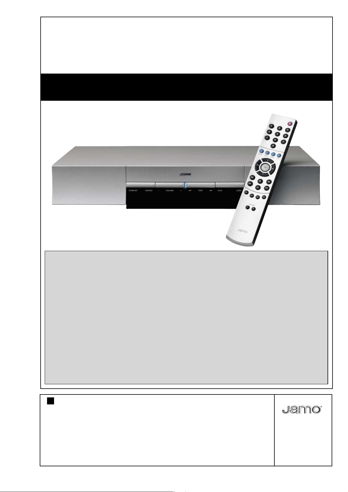
DVR 50
HOME CINEMA SYSTEM
Jamo Service manual
IMPORTANT NOTICE
This manual is intended for Jamo retailers and their appointed service representatives. Jamo assume that basic service procedures inherent to
the industry, and specifi cally Jamo products, are already known and understood by the users and will for that reason not be restated here.
WARNING Failure to follow appropriate service and safety procedures when servicing this product may result in personal injury,
destruction of expensive components and equipment or/and shortening the product life or/and failure of the product
to perform as specifi ed. For these reasons Jamo strongly advice product owners that all service required should be
performed by an authorized Jamo retailer or the appointed service representative.
WARNING Static discharge can destroy expensive components, equipment or/and shorten the product life. Discharge any static
electricity accumulated in your body or materials in the vicinity of the workplace by grounding.
IMPORTANT This manual does not in its self constitute authorization, certifi cation or establish a principle agent or partner
relationship of any form.
IMPORTANT Jamo continually strive to improve their products and as a consequence of these modifi cations are inevitable. Specifi cations
are subject to change without notice or obligation to retrofi t. Should any discrepancy appear in this manual, please
contact Jamo Call center.
IMPORTANT
Disconnect all mains power before disassembly or part replacement. Recheck all work before reapplying mains power to the unit.
Contents
To service personnel .......... 2 - 4 Faultfi nding .................... 9 Remote control ................................ 56
Specifi cations ........................... 5 Audio board ................. 10 Cabinet ...................................... 57 - 61
DVR 50 diassembly .................6 VFD board .................... 23 Cables ............................................... 62
DVR 50
System overview ......................7 MPEG board ................ 25 Legend and abbreviations .............. 63
Block diagram ..........................8 Loader .......................... 54
DVR 50 - Rev. 011105-2
Rev. 011105-2
1
Page 2
To service personnel
Preparing Jamo products for shipment
If possible, use the original packing material for any shipping. Otherwise, repack the product
using:
• A reinforced cardboard box, strong enough to carry the weight of the product.
• At least 6 cm / 2.36 inches of shock-absorbing material around the product.
• Nonabrasive dust-free material for the other parts.
• Nonabrasive wrapping for the product. (Dust and dirt cover)
• Repack the product in a manner to ensure that it cannot shift in the box during transport.
Never ship products, like speakers and subwoofers, with spikes mounded. Spikes can penetrate
the cardboard and other packing material causing serious damage.
Never pack accessories, mains cord etc. in a way that it could damage the product.
The Jamo warranty does not cover damage during shipment. The product warranty is described
in the user’s manual and on the Jamo homepage.
Receiving products
When products are received, the following procedure should be followed:
1. Inspect the outer box for damage.
2. Carefully unpack all items from the box and check for damage.
3. Check that nothing is missing according to the delivery note.
4. If you note any physical damage not stated in the fault description or missing items,
contact the sender immediately and clarify the matter.
Damage during transport is not covered by the Jamo warranty.
How to order spare parts
When ordering spare parts, we would like you to state both the Part description and Item no.
This is to avoid times consuming misunderstandings and extra shipments.
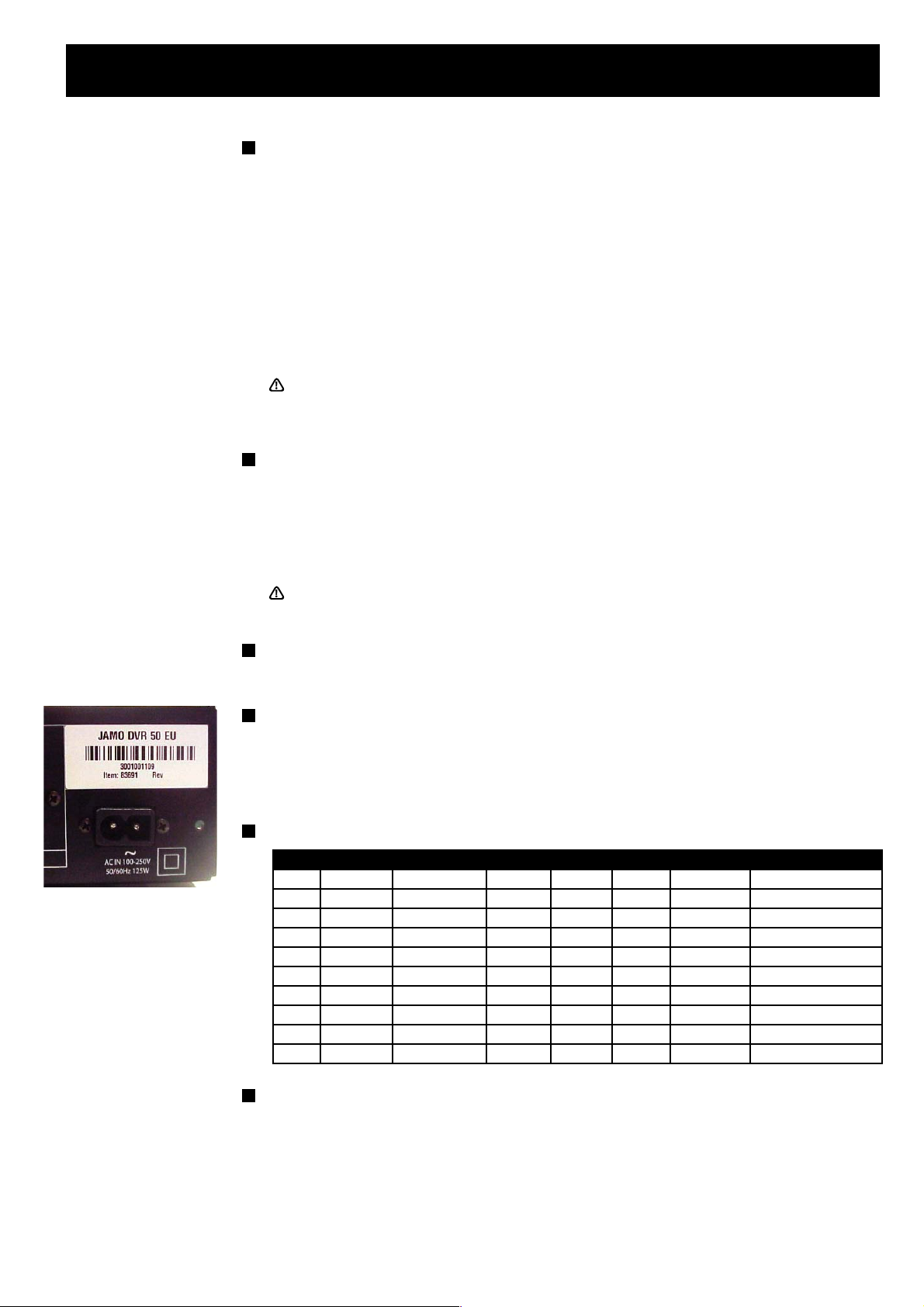
DVR 50 Serial No.:
On all DVR 50 units you will fi nd a Serial number on the rear panel. Fig. 44-0401/8
The number is made up of tree sections. The fi st section is the factory code (two digits). The
XX
next section is the revision number (two digits). The rest of the serial number is a running serial
number starting with 3001001100.
DVR 50 models:
Item No. Rear label Tuner model Region code Power cable Video cable TV System Countries
83990 DVR 50 - US KST-MV011MA0-B0 1 US S-video NTSC US, Canada
83991 DVR 50 - EUR KST-MV114MA1-B0 2 EU Scart PAL Europe, South Africa, Israel
83992 DVR 50 - UK KST-MV114MA1-B0 2 UK Scar t PAL UK, Ireland
83993 DVR 50 - AUS KST-MV011MA0-B0 4 AUS S-video PAL Australia, New Zealand
83994 DVR 50 - LA KST-MV011MA0-B0 4 US S-video NTSC Argentina, Brazil, Mexico
83995 DVR 50 - CHN KST-MV011MA0-B0 6 EU S-video PAL China
83996 DVR 50 - TW KST-MV011MA0-B0 3 US S-video NTSC Taiwan
83997 DVR 50 - ASIA KST-MV011MA0-B0 3 EU S-video PAL Korea, Singapore
83998 DVR 50 - RUS KST-MV114MA1-B0 5 EU S-video PAL Russia
83999 DVR 50 - CHILE KST-MV011MA0-B0 4 EU S-video PAL Chile
Manual revision No.
On the front page, in bottom right hand corner, you will fi nd the manual revision number. The
number is basically the release date followed by a product status number. (day month year status No.)
The following list shows the products status No.:
• 1 is for products still in production.
• 2 is for discontinued products for which spare parts are still available.
• 3 is for discontinued products for which spare parts are no longer available.
Please note! The latest service manuals are available for download on the Jamo homepage.
DVR 50 - Rev. 011105-2
4
Page 3

Specifi cations
System .....................................................................................................................................................................DVD-Receiver
Weight (kg/lb) .....................................................................................................................................................................4,4/9,7
Dimensions (HxWxD/mm/in) .........................................................................................70x430x295/2,76x16,93x11,61
PowerConsumption ................................................................................................................................................. Max 120W
RatedOutput6Ohm1Khz10 ......................................................................................................................... 2 x 50/50/2 x 50
RatedOutput6Ohm1Khz1 ........................................................................................................................... 2 x 35/35/2 x 35
TuningRange ....................................................................................................................87,5 - 108.0Mhz / 522 - 1611 kHz
RadioSNRatio ..................................................................................................................................................................... > 70dB
DiscFormats .....................................................CD/CD-R/CD-RW/DVD-Video/DVR-R/DVD-RW/DVD+R/DVD+RW/
VideoInputs ................................................................................................................................................................................ No
ProgressiveScan .................................................................................................................................................. Yes, PAL/NTSC
VideoOutputs .......................................................................................... Composite, S-Video, RGB(Scart), Component
PowerConsumption ................................................................................................................................................. Max 120W
AudioOutputs ................................................................................................................................1x Analog/ 1x Optical Dig.
DVR 50 - Rev. 011105-2
5
Page 4
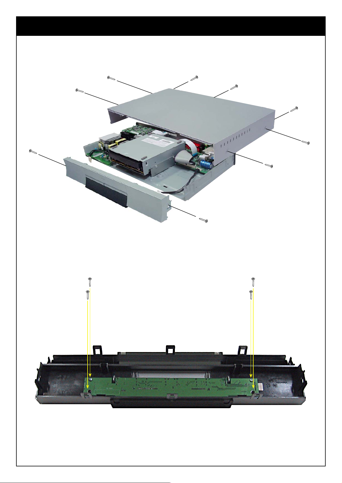
DVR 50 diassembly
DVR 50 - Rev. 011105-2
6
Page 5
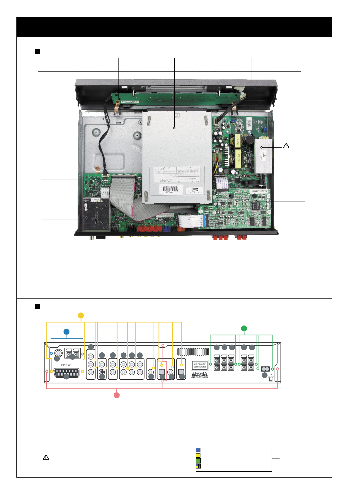
DVR 50 System overview
Top view
6
2
51 3
High voltage
Do not touch
during operation!
4
1 DVD Loader
2 Tuner DVD receiver module EU/US
3 PSU assy Audio DVR 50
4 Audio board
5 VFD board
6 MPEG board
Rear view
22
21
4
2
1
3
5 7
6
8 9 10
24
Detailed overview of the back panel
1. FM antenna
2. AM antenna
3. SCART connector
4. Component video output
5. Composite video output
6. S-Video output
7. Analog audio output
Zoom for more information
* For board replacement remove following screws
8. TV analog input
9. Video analog input
10. Auxiliary analog input
11. Subwoofer output
12. Optical audio input
13. Coaxial audio input
14. Optical audio output
23
151617
11
12 13
14
15. Surround speaker centre out
16. Surround speaker right out
17. Surround speaker left out
18. Right speaker out
19. Left speaker out
20. AC input
21. Tuner
22. Audio board
23. PSU board
21. - 22. - 23. - 24. Rear Panel
18
19
20
For board replacement
remove following screws
DVR 50 - Rev. 011105-2
7
Page 6
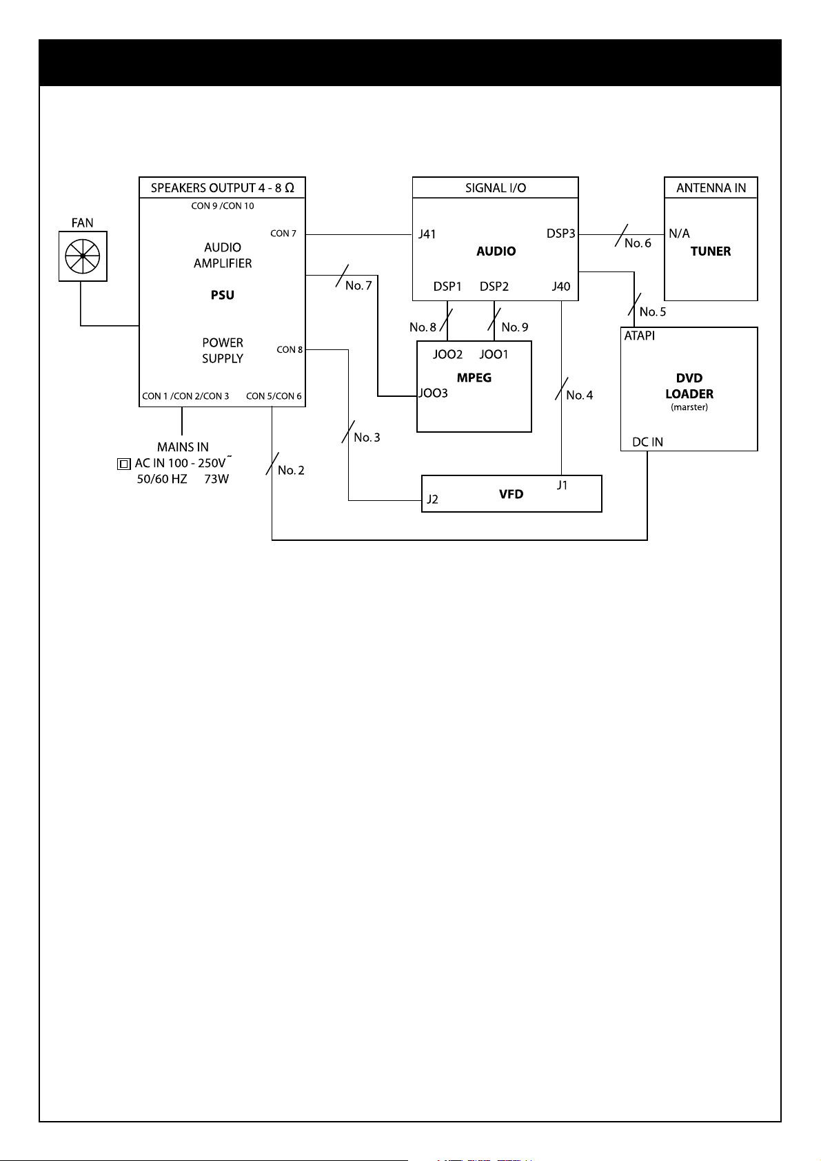
DVR 50 Block diagram
DVR 50 - Rev. 011105-2
8
Page 7

DVR 50 Faultfi nding
The following guide is base on service reports sent in by service partner’s world wide. Try the suggested corrections in
the same order as they are listed.
Before replacing modules and components always make sure that product in front of you has the latest Firmware
version. The Firmware version can be checked in the hidden menu. To access the hidden menu:
Press LOAD to open the loader tray
Press INFO followed by 2,7,6 and you have now accessed the hidden menu.
Press MENU to close the hidden menu again.
The latest Firmware (instructions included) can be downloaded from the Jamo website under download.
Symptom Possible cause Correction
The unit will not power up. • Bad internal cable connections.• Burned FUSE
The unit will not BOOT. • Faulty or incorrectly burned Firmware CD.•
No light in the display. • Bad internal cable connections.• Defective
The LOADER tray will not open. • Bad internal cable connections.• Defective
“Noisy” LOADER • Out of balance- or off centred discs.• Loos
Audio faults.Front speakers (Left/Right)Center
speaker.SUR speakers (Left/Right)
Audio faults.No Radio.No TV/Video/Aux.No I/O
digital/optical
Faults on TV signals or the 12V controls.
(Missing voltage)
The DVR 50 unit does not respond to
commands from the remote control.
The DVR 50 does not respond to any
commands.
The DVR 50 does not respond to some
operating commands during playback.
on the PSU module.• Defective PSU module.
Bad internal cable connections.• Defective
MPEG module.• Defective LOADER module.
VFD module.• Defective PSU module.•
Defective MPEG module.
Audio module.• Defective MPEG module.•
Defective VFD module.• Defective LOADER
module.
LOADER brackets.• Copy protection.• Poor
quality or poorly recorded media.• Defective
LOADER module.
• Copy protection.• Bad internal cable
connections.• Defective Audio module.•
Defective PSU module.
• Bad internal cable connections.• Defective
Audio module.• Defective MPEG module.
• Bad internal cable connections.• Defective
MPEG module.
• No batteries are inserted in the remote
control.• The batteries are worn out.• Bad
internal cable connections.• Defective VFD
module.• Defective MPEG module.
• Power supply fl uctuations or other
abnormalities such as static electricity may
interrupt correct operation.• The DVR 50
operation may have been interrupted by a non
standard disc.
• Operations may not be permitted by the disc. • Read the instructions on the disc.
• Secure all cable connections.*(1)• Replace
FUSE and check unit.*(2)• Replace the PSU
module.
• Open the loader tray*(3) and try with a new
CD.• Secure all cable connections.• Replace the
MPEG module.• Replace the LOADER module.
• Secure all cable connections.• Replace the
VFD module.• Replace the PSU module.•
Replace the MPEG module.
• Secure all cable connections.• Replace the
Audio module.• Replace the MPEG module.•
Replace the VFD module.• Replace the LOADER
module.
• Discard the bad discs.• Tighten the LOADER
bracket. (see instruction under LOADER
module)• Some copy protection systems will
disrupt the playing of music. Check with other
discs.• Discard the bad discs.• Replace the
LOADER module.
• Some copy protection systems will disrupt
the playing of music. Check with other discs.•
Secure all cable connections.• Replace the
Audio module.• Replace the PSU module.
• Secure all cable connections.• Replace the
Audio module.• Replace the MPEG module.
• Secure all cable connections.• Replace the
MPEG module.
• Insert new batteries.(2 x “AAA” R6P)• Replace
with new batteries.(2 x “AAA” R6P)• Secure all
cable connections.• Replace the VFD module.•
Replace the MPEG module.
• In order to completely reset the DVR 50,
unplug the power cable from the AC outlet.
Wait at least 30 seconds to allow all capacitors
to fully discharge. (personal settings will not
be affected)
*(1) Especially REV. 01 units are prone to bad internal cable connections do to cable length and ferrite blocks.
*(2) The PSU module FUSE is located under the heat sink. Warning! Do not replace the FUSE unless the mains cord has
been removed! High voltage Warning! Do not touch the heat sink during operation!
*(3) The loader module can be opened by pressing the STANDBY button simultaneously with powering up the unit.
(Reconnecting the power cable)
DVR 50 - Rev. 011105-2
9
Page 8
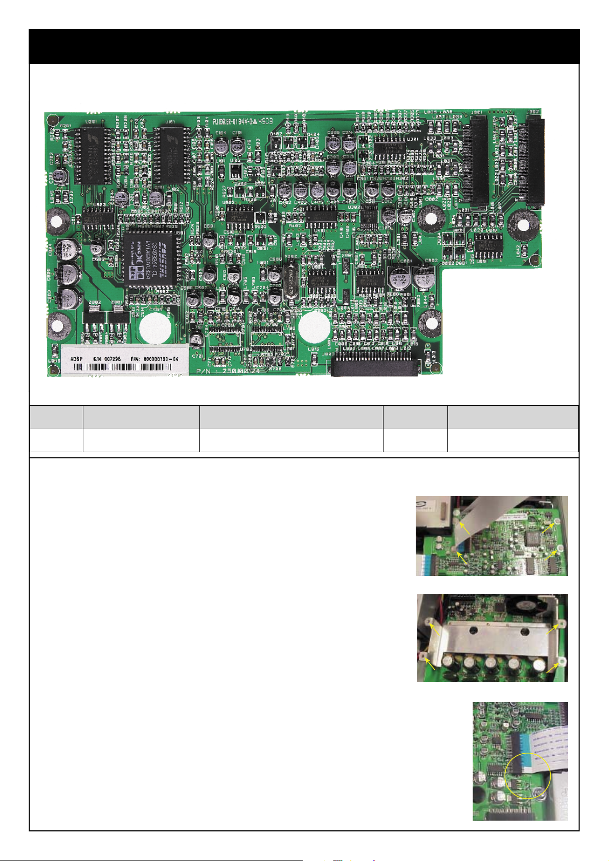
DVR 50 Audio board
DVR 50 Electronic moduls
Ref. No. Item No.
1
74101 PCB assy Audioboard DVR-50
Replacing the DVR 50 Audio board
• Disconnect the power cord from the AC outlet and take all necessary ESD
precaution.
• Remove the Lid. (See instruction under Lid)
• Disconnect all cables going to and from the Audio board.
• Unscrew the 4 screws holding the Audio board. See picture 44-0400/3
• Replace the board with a new Audio board. Note 1
• Reconnect the cables. Note 2
• Test the DVR 50 unit.
Important notes!
Note 1:
If washers is present. Be careful not to loose any of the isolation washers when
removing the board. There must be two plastic washers between the Audio
board and the PSU heat sink. See picture 44-0400/2. after Rev. 4 boards dos not
have washers.
Part description
PCS.
1
Fig. 44-0400/3
Fig. 44-0400/2
Remarks
Rev. ≥ 4
Note 2:
Early models (approximately 30 units) got a sliced up Audio - MPEG cable. Special
care should be taken when refi tting it after service. The sliced cables are only
seen on board Rev. 2 boards. See picture 44-0401/4
Fig. 44-0401/4
DVR 50 - Rev. 011105-2
10
Page 9
A B C D E F
1
2
3
4
DVR 50 - Rev. 011105-2
AUX_L
AUX_R
VCR_L
VCR_R
TUN_L
TUN_R
TV_L
TV_R
+3.3V
GND
Sigma Connector
SIGMA_CON.SCH
Power Supply
PWR_SUP.SCH
Clock
CLOCK.SCH
Page 11
+3.3V
GND
LINEOUTL
LINEOUTR LFE
DIT_SPDIF
OPT_SPDIF
DVD_SPDIF
COAX_SPDIF
AUX_L
AUX_R
VCR_L
VCR_R
TUN_L
TUN_R
TV_L
TV_R
+12VR
-12VR
VCC5V
GNDR
+3.3V CLK_SEL
A_GND
/SPDIF_ERR_SENSE
/RESET
HI_MCLK
Page 8
+3.3V
+2.5V
Page 5
HI_MCLK
MCLKGND
+12V
GND
+3.3V
GND
A_GND
Equalizer DSP
+3.3V
+3.3V
GND
GND
SCL
SDA
/INT
-12V
+5V
+12V
-12V
+5V
+3.3V
+2.5V
GND
+3.3V
+2.5V
GND
+12V
-12V
+3.3V
A_GND
AUX_L
AUX_R
VCR_L
VCR_R
TUN_L
TUN_R
TV_L
TV_R
DSP
+3.3V
+2.5V
GND
SCL
SDA
/INT
/RESET
/SPDIF_ERR_SENSE
/A_RESET
/ERR_RCVY
/MUTE
CLK_SEL
MCLK
DSP.SCH
Analog Input
+12V
-12V
+3.3V
A_GND
AUX_L
AUX_R
VCR_L
VCR_R
TUN_L
TUN_R
TV_L
TV_R /RESET
ANA_IN.SCH
Page 6
EQ_MCLK
EQ_SCLK
EQ_LRCLK
EQ_DATA1
EQ_DATA2
EQ_DATA3
DAC_MCLK
DAC_SCLKSPDIF_ERR
DAC_LRCLK
DAC_DATA
DIT_MCLK
DIT_SCLK
DIT_LRCLK
DIT_DATA
/Audio
DIR_MCLK
DIR_SCLK
DIR_LRCLK
DIR_DATA
SEL_A
SEL_B
ADC_MCLK
ADC_SCLK
ADC_LRCLK
ADC_DATA
Page 2 Page 3
ADC_DATA
ADC_LRCLK
ADC_SCLK
ADC_MCLK
SEL_B
SEL_A
/RESET
SCL
SDA
EQ_MCLK
EQ_SCLK
EQ_LRCLK
EQ_DATA1
EQ_DATA2
EQ_DATA3
EQ_DSP.SCH
+3.3V
GND
S/PDIF Receiver
+3.3V
GND
OPT_SPDIF
DVD_SPDIF
COAX_SPDIF
S/PDIF_RX.SCH
DIR_DATA
DIR_LRCLK
DIR_SCLK
DIR_MCLK
SPDIF_ERR
Page 7
AMP_MCLK
AMP_SCLK
AMP_LRCLK
AMP_DATA1
AMP_DATA2
AMP_DATA3
Page 9 Page 10
/INT
SDA
SCL
/RESET
MCLK
+3.3V
+5V
GND
S/PDIF Transmitter
+3.3V
+5V
GND DIT_LRCLK
/RESET
DIT_SPDIF
S/PDIF_TX.SCH
/Audio
DIT_DATA
DIT_SCLK
DIT_MCLK
Power Supply Connector
+12VR
-12VR
VCC5V
GNDR
LFE
/A_RESET
/ERR_RCVY
/MUTE
SCL
SDA
AMP_MCLK
AMP_SCLK
AMP_LRCLK
AMP_DATA1
AMP_DATA2
AMP_DATA3
+3.3V
GND
A_GND
Page 12
Analog Output
+3.3V
GND
A_GND
LINEOUTL
LINEOUTR
ANA_OUT.SCH
PSU_CON.SCH
DAC_DATA
DAC_LRCLK
DAC_SCLK
DAC_MCLK
/A_RESET
/RESET
11
Components having special characteristics or critical for safety are
identifi ed by
5
specifi ed by the manufacturer.
Schematic diagram is subject to change without notice.
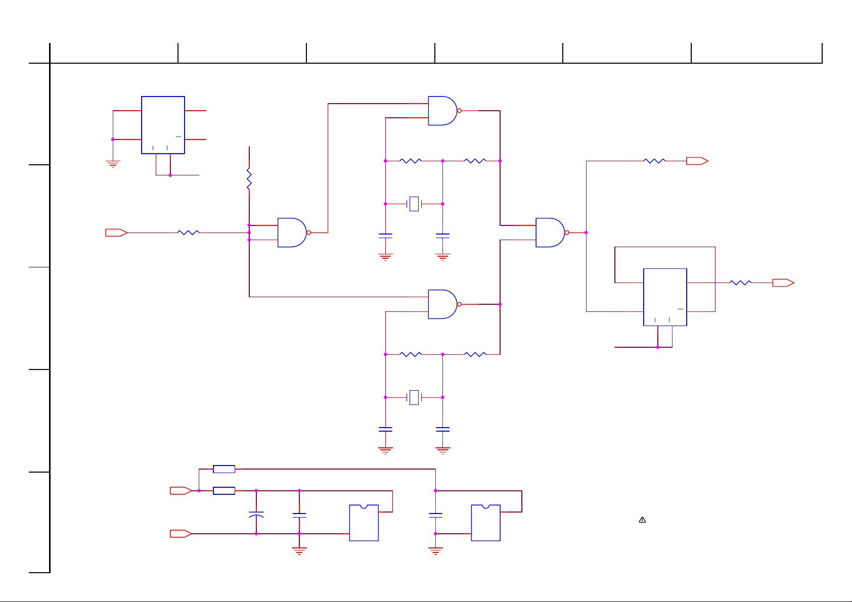
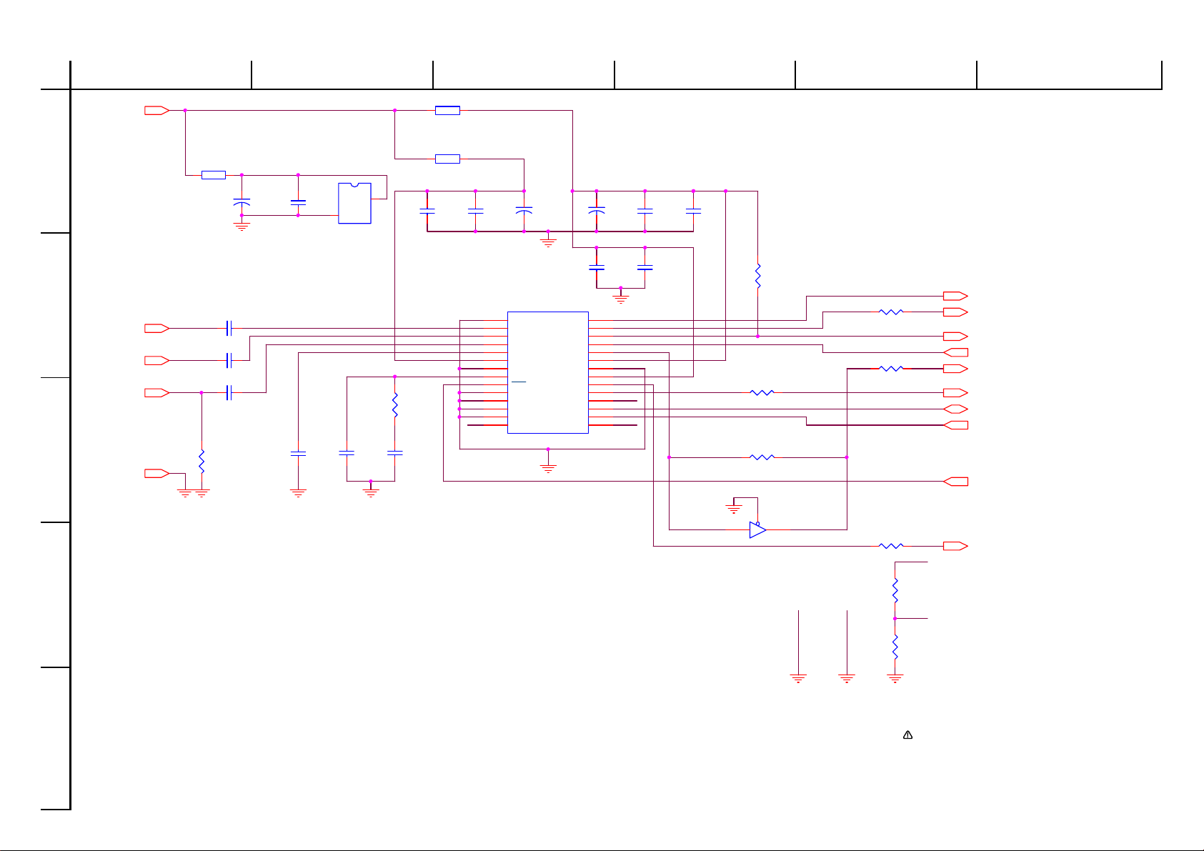
Schematic diagram - Audio board 1/10
mark and must be replaced with components
11
Page 10
A B C D E F
1
2
3
4
DVR 50 - Rev. 011105-2
AUX_L
AUX_R
VCR_L
VCR_R
TUN_L
TUN_R
TV_L
TV_R
SEL_A
SEL_B
+12V
A_GND
-12V
+3.3V
U301 HEF40 52B
12
X0
14
R322 0R0 C304
R323 0R0
R324 0R0
R325 0R0
R326 0R0
R327 0R0
R328 0R0
R329 0R0
R306
R305
100K
100K
Z301
BZX84-C4V7
Z302
BZX84-C4V7
+3.3VD +3.3VA
C307
10uF/16V
R307
100K
+
C313
10uF/16V
+
C314
10uF/16V
R308
100K
L301
BEAD
C308
100nF
C301
100nF
C302
100nF
C309
10uF/16V
C310
100nF
R314
120R
R317
120R
R315
120R
R318
120R
R301
100K
R302
100K
R316
120R
R319
120R
R303
100K
R304
100K
15
11
1
5
2
4
10
9
6
7
X1
X2
X3
Y0
Y1
Y2
Y3
A
B
EN
VEE
VDD16GND
13
X
3
Y
8
C303
10uF/16V
R309
100K
C305
10uF/16V
R311
100K
+
+
+3.3VD
R310
150R
10nF
R312
150R
C306
10nF
R320
Not Mounted
R321
0R0
14
13
10
6
CS5333-KZ
+3.3VD +3.3VA
1
VL
AINL
AINR
TST
GND
5
U302
VA
REF_GND
FILT+
MCLK
SCLK
LRCK
SDATA
RST
DIF
DIV
C315
100nF
C316
100nF
C311
1uF/50V
15
VQ
12
11
2
3
7
4
16
9
8
+3.3VD
C312
1uF/50V
R313
47K
ADC_MCLK
ADC_SCLK
ADC_LRCLK
ADC_DATA
/RESET
12
Components having special characteristics or critical for safety are
identifi ed by
5
specifi ed by the manufacturer.
Schematic diagram is subject to change without notice.
Schematic diagram - Audio board 2/10
mark and must be replaced with components
12
Page 11

A B C D E F
1
2
3
4
DVR 50 - Rev. 011105-2
/RESET
DAC_DATA
1
2
DAC_SCLK
DAC_LRCLK
DAC_MCLK
GND
A_GND
Connection between analog and digital ground is done here.
L402
BEAD
R412
Not Mounted
L403
BEAD
3
4
5
6
7
8
U401 CS4340
RST
SDATA
SCLK/DEM
LRCK
MCLK
DIF1
DIF0
DEM0
MUTEC
AOUTL
AGND
AOUTR
REF_GND
FILT+
VA
VQ
+3.3VD
C401
100nF
C403
10uF/16V
+
16
15
14
13
12
11
10
9
R407
3K3
R408
10K
C407
+
1uF/50V
R409
10K
R410
3K3
Q401
2N3904
C408
100nF
+3.3VD
C405
10uF/16V
+
C409
+
1uF/50V
Q402
2N3906
R411
10K
R402
560R
R401
10K
R405
560R
R404
10K
C410
100nF
C402
10uF/16V
+
C404
1.5nF
C406
1.5nF
BEAD
R403
3K3
R406
3K3
L401
Q403
2N3904
Q404
2N3904
+3.3V
LINEOUTL
LINEOUTR
13
R413
5
/A_RESET
10K
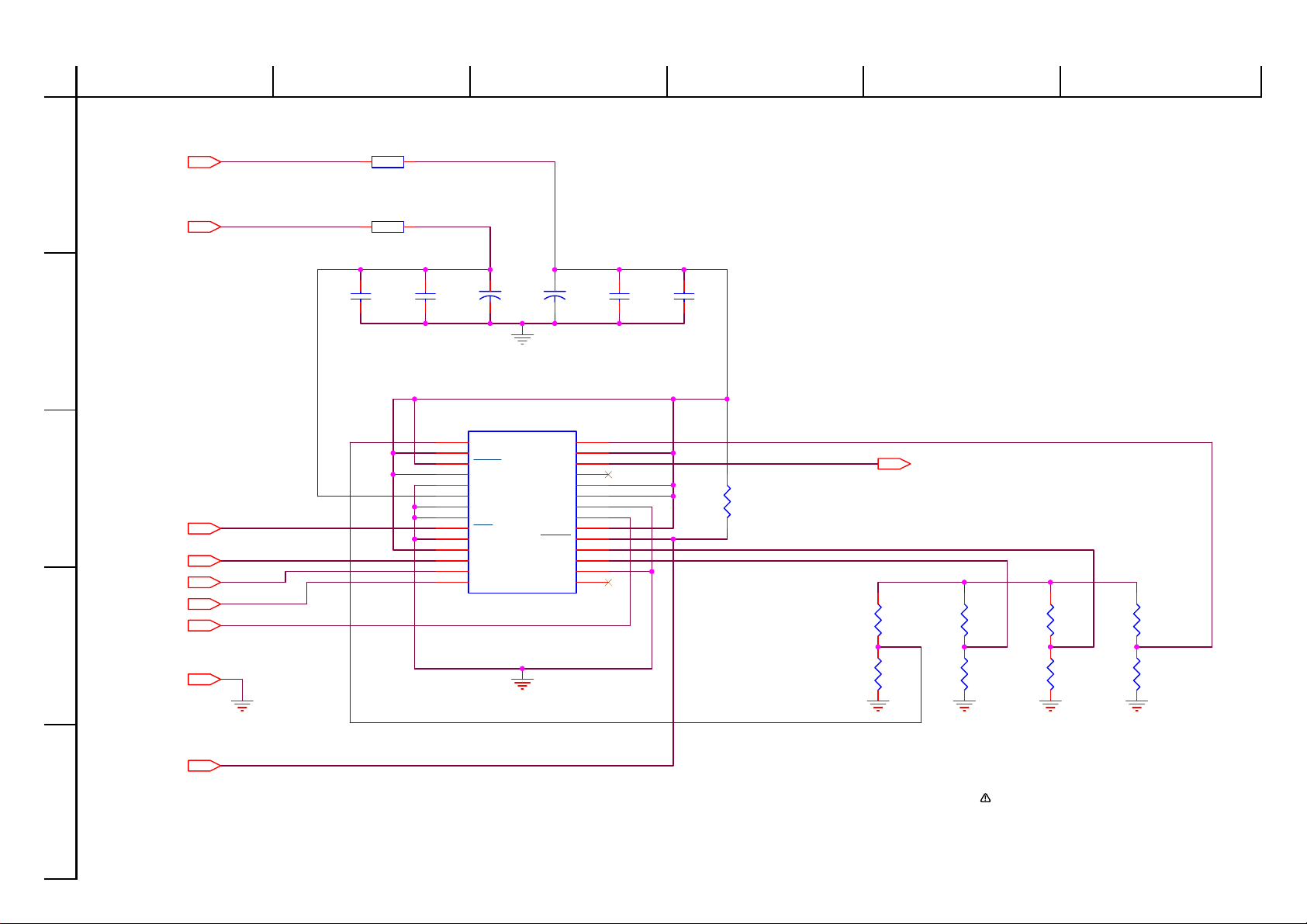
Schematic diagram - Audio board 3/10
Components having special characteristics or critical for safety are
identifi ed by
mark and must be replaced with components
specifi ed by the manufacturer.
Schematic diagram is subject to change without notice.
13
Page 12
A B C D E F
U902B 74HC74
1
12
D
11
CLK
10
2
CLK_SEL
9
Q
8
Q
R13S
+3.3VD
R907
Not Mounted
+3.3VA
R908
0R0
1
2
U901A
74HC00
3
C901
10pF
3
U901B
4
5
74HC00
R901
1M
X901
Not Mounted
U901D
12
13
74HC00
R903
1M
X902
24.576 MHz
C902
10pF
6
R902
220R
11
R904
220R
9
10
U901C
74HC00
R906
51R
8
U902A 74HC74
2
+3.3VD
D
3
CLK
S4R
Q
Q
1
HI_MCLK
R905
5
6
33R
MCLK
DVR 50 - Rev. 011105-2
14
4
L902
BEAD
+3.3V
5
GND
L901
BEAD
C906
1uF/50V
C905
100nF
U901E
7
74HC00
+3.3VA
14
C903
10pF
C904
10pF
+3.3VD
U902C
C907
100nF
7
Vcc
Vss
74HC74
14
Components having special characteristics or critical for safety are
identifi ed by
mark and must be replaced with components
specifi ed by the manufacturer.
Schematic diagram is subject to change without notice.
Schematic diagram - Audio board 4/10
14
Page 13
A B C D E F
GPIO10
+2.5VD
+2.5VD
+2.5VD+2.5VD
+2.5VD
+2.5VD
GPIO10
+3.3VD
+2.5VA+2.5VD
+3.3VD
+3.3VD
+3.3VD
+2.5VA
+3.3VD
+3.3VD
+3.3VD
+3.3VD
EQ_D ATA1
EQ_D ATA2
EQ_D ATA3
EQ_LRCLK
EQ_SCLK
EQ_MCLK
DIR_LRCLK
DIR_SCLK
DIR_DATA
ADC_LRCLK
ADC_SCLK
ADC_DATA
DIR_MCLK
DAC_DATA
DAC_LRCLK
DAC_MCLK
SCL
CLK_SEL
DIT_MCLK
DIT_SCLK
DIT_LRCLK
DIT_DATA
/Audio
MCLK
ADC_MCLK
DAC_SCLK
SPDIF_ERR
/A_RESET
/ERR_RCVY
SEL_A
/RESET
SEL_B
SDA
/INT
/MUTE
GND
+3.3V
+2.5V
/SPDIF_ERR_SENSE
Title
Size Do cument Number Re v
DSP 3.0
Audio Processing Board
A3
Amplifier error signal FF
Revision history
3.0: GPIO5 used to reset amp, R528 added.
3.0: Ports DET_AUX, DET_VCR, DET_TV is removed.
3.0: R529 & R530 added.
3.0: D503 added.
3.0: R508-R511 & R527changed to 1K.
3.0: C516-C519 added.
A capacitor pair (1uF and 0.1uF) must be placed at each power pin
C509
100nF
R512
10K
C511
100nF
+
C503
1uF/50V
C502
100nF
R525
33R
U502A
74HC74
D
2
CLK
3
Q
5
Q
6
S4R
1
R501
4K7
R530
3K3
R524 33R
C519
100nF
R522
33R
L501
BEAD
R529
3K3
R527
1K
D501
BAV99
C514
220pF
R513
3K3
R528
4K7
+
C505
1uF/50V
R520
200K
C504
100nF
U502C
74HC74
Vcc
14
Vss
7
R502
4K7
Q502
2N3904
C517
100nF
U502B
74HC74
D
12
CLK
11
Q
9
Q
8
R13S
10
R521
33R
R517
10K
+
C507
1uF/50V
R508
1K
R514
3K3
R507
4K7
R515
4K7
C506
100nF
R519
10K
C510
100nF
R523
33R
R503
3K3
R518
10K
R526 4K7
D502
BAV99
U503A
74LVC157A
1A
2
1B
3
2A
5
2B
6
3A
11
3B
10
4A
14
4B
13
1Y
4
2Y
7
3Y
9
4Y
12
G
15
A/B
1
D503
BAV99
+
C508
1uF/50V
R509
1K
R510
1K
R504
3K3
+
C501
1uF/50V
R506
4K7
C516
100nF
U503B
74LVC157A
Vcc
16
Vss
8
R516
4K7
+
C512
2.2uF/50V
Q501
2N3904
C513
10nF
R505
4K7
U501
CS493264-CL
VD
1
DGND1
2
AUDATA3
3
GPIO104GPIO11
5
SCDIN
6
SCL
7
GPIO7
8
GPIO6
9
GPIO5
10
GPIO4
11
VD2
12
DGND2
13
GPIO3
14
GPIO2
15
GPIO1
16
GPIO0
17
CS18SDA19INT20GPIO821SDATAN122VD323DGND324SCLKN125LRCLKN126SDATAN227SCLKN2
28
LRCLKN2
29
CLKIN
30
CLKSEL
31
FILT2
32
FILT1
33
VA
34
AGND
35
RESET
36
DD
37
DC
38
AUDATA2
39
AUDATA1
40
AUDATA0
41
LRCLK
42
SCLK
43
MCLK
44
C518
100nF
R511
1K
1
2
3
DVR 50 - Rev. 011105-2
15
4
5
Schematic diagram - Audio board 5/10
identifi ed by
specifi ed by the manufacturer.
Components having special characteristics or critical for safety are
mark and must be replaced with components
Schematic diagram is subject to change without notice.
15
Page 14
A B C D E F
R701 0R0
R702 0R0
R703 0R0
R704 0R0
1
R705 0R0
R706 0R0
DVR 50 - Rev. 011105-2
16
U701
EQ_DATA1
EQ_DATA2
EQ_DATA3
EQ_MCLK
EQ_SCLK
EQ_LRCLK
2
/RESET
SDA
SCL
14
SDIN1
15
SDIN2
16
SDIN3
17
SDIN4
37
ORIN
9
MCLKI
1
SCLKIN
38
LRCLK
2
PWRDN
26
RST
18
GPIO0
19
GPIO1
20
GPIO2
21
GPIO3
3
REG_EN
10
TEST
11
MICROCLK_DIV
22
PLL0
23
PLL1
24
CS0
25
CS1
27
I2CM_S
12
I2C_SDA
13
I2C_SCL
Not Mounted
SDOUT1
SDOUT2
SDOUT3
SCLKOUT1
SCLKOUT2
MCLKO
XTALI
XTALO
AVDD_CAP
A_VDSS
AVSS
DVDD_CAP
VDSS
DVSS
TAS3103
30
32
33
35
36
34
4
5
6
7
8
29
31
28
+3.3VA1
AVSS1
+3.3VD
R707
33R
C707
10nF
C708
10nF
R708
33R
C706
10nF
L703
BEAD
C705
10nF
AMP_DATA1
AMP_DATA2
AMP_DATA3
AMP_SCLK
AMP_MCLK
AMP_LRCLK
3
U702
14
SDIN1
15
SDIN2
16
SDIN3
17
SDIN4
37
ORIN
9
MCLKI
1
SCLKIN
38
LRCLK
2
PWRDN
26
RST
4
+3.3VD
18
GPIO0
19
GPIO1
20
GPIO2
21
GPIO3
3
REG_EN
10
TEST
11
MICROCLK_DIV
22
PLL0
23
PLL1
24
CS0
25
CS1
27
I2CM_S
12
I2C_SDA
13
I2C_SCL
Not Mounted
5
SDOUT1
SDOUT2
SDOUT3
SCLKOUT1
SCLKOUT2
MCLKO
XTALI
XTALO
AVDD_CAP
A_VDSS
AVSS
DVDD_CAP
VDSS
DVSS
TAS3103
30
32
33
35
36
34
4
5
6
+3.3VA2
7
AVSS2
8
C711
+3.3VD
10nF
C712
10nF
29
31
28
C710
10nF
L704
BEAD
C709
10nF
+3.3V
GND
L701
BEAD
+
C701
1uF/50V
identifi ed by
L705
BEAD
C702
100nF
L702
BEAD
+3.3VA1+3.3VD
C704
+
C703
100nF
1uF/50V
AVSS1 AVSS2
+
C713
1uF/50V
+3.3VA2
C714
100nF
Components having special characteristics or critical for safety are
mark and must be replaced with components
specifi ed by the manufacturer.
Schematic diagram is subject to change without notice.
Schematic diagram - Audio board 6/10
16
Page 15
A B C D E F
1
2
3
4
DVR 50 - Rev. 011105-2
+12VR
-12VR
VCC5V
GNDR
GND
R801
10R
R802
10R
+
+
+
C801
47uF/16V
C802
47uF/16V
C803
47uF/16V
+12V
-12V
4
Z801
AMS117
4
VIN3VOUT2ADJ
1
4
Z802
AMS117
4
VIN3VOUT2ADJ
1
R803
301R
R804
510R
R805
301R
R806
301R
+
+
C804
47uF/16V
C805
47uF/16V
+3.3V
+5V
+2.5V
17
Components having special characteristics or critical for safety are
identifi ed by
5
specifi ed by the manufacturer.
Schematic diagram is subject to change without notice.
Schematic diagram - Audio board 7/10
mark and must be replaced with components
17
Page 16
A B C D E F
R102
1K
C110
220nF
L101
BEAD
L102
BEAD
C103
1nF
AD0
C102
100nF
1
2
3
4
5
6
7
8
9
10
11
12
13
14
C101
10uF/16V
U101
RXP3
RXP2
RXP1
RXP0
RXN
VA+
AGND
FILT
RST
RXP4
RXP5
RXP6
RXP7
AD0
CS841 6-CS
OLRCK
OSCLK
SDOUT
OMCK
RMCK
VD+
DGND
VL+
GPO0
GPO1
AD2
SDA
SCL
AD1
28
27
26
25
24
23
22
21
20
19
18
17
16
15
C104
10uF/16V
C107
100nF
AD2
AD1
C105
100nF
C108
1nF
VL+
C106
1nF
R103
47K
R109 Not Mounted
R107 Not Mounted
U102A
1
NC7SZ125M5
42
R104 33R
R105 33R
R110 4K7
DIR_LRCLK
DIR_SCLK
DIR_DATA
MCLK
DIR_MCLK
/INT
SDA
SCL
/RESET
SPDIF_ERR
VL+
+3.3V
1
L103
BEAD
C115
10uF/16V
C116
100nF
U102B
5
3
NC7SZ125M5
2
C112
R101
75R
10nF
C113
10nF
C114
10nF
C111
10nF
C109
10nF
This ground should be returned
directly to AGND of U1
OPT_SPDIF
DVD_SPDIF
COAX_SPDIF
3
GND
DVR 50 - Rev. 011105-2
18
R108
4
AD1AD0
I2C Adress: 0010 + AD2 + AD1 + AD0
Components having special characteristics or critical for safety are
identifi ed by
5
specifi ed by the manufacturer.
Schematic diagram is subject to change without notice.
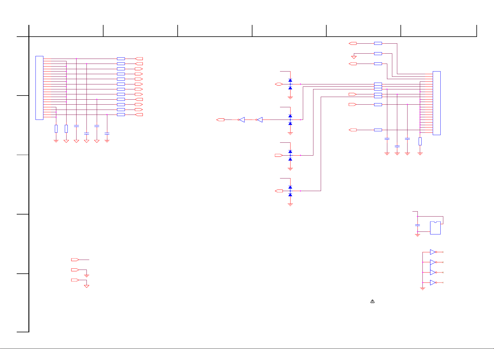
Schematic diagram - Audio board 8/10
Not Mounted
AD2
R106
47K
mark and must be replaced with components
18
Page 17
A B C D E F
1
2
3
4
DVR 50 - Rev. 011105-2
+3.3V
+5V
/RESET
DIT_LRCLK
DIT_SCLK
DIT_DATA
DIT_MCLK
GND
L201
BEAD
L202
BEAD
C203
1nF
C202
100nF
U201 CS8405-CS
1
COPY/C
2
VL2+
3
EMPH
4
SFMT0
5
SFMT1
6
VD+
7
DGND
8
DGND
9
RST
10
APMS
11
TCBLD
12
ILRCK
13
ISCLK
14
SDIN
C201
10uF/16V
ORIG
VL4
TXP
TXN
H/S
VL+
DGND
OMCK
VL3
AUDIO
CEN
TCBL
C204
10uF/16V
28
27
26
25
24
23
22
21
20
19
18
U
17
V
16
15
C205
100nF
C206
1nF
VL+
R209
Not Mounted
DIT_SPDIF
R201
0R0
R202
Not Mounted
R203
Not Mounted
R204
0R0
R205
Not Mounted
R206
0R0
VL+
R207
Not Mounted
R208
0R0
19
Orig BitU BitV BitC Bit
/Audio
Components having special characteristics or critical for safety are
identifi ed by
5
specifi ed by the manufacturer.
Schematic diagram is subject to change without notice.
Schematic diagram - Audio board 9/10
mark and must be replaced with components
19
Page 18
A B C D E F
1
2
3
Audio Signal Connector
J001
1
2
3
4
5
6
7
8
9
10
11
12
13
14
15
16
17
18
19
20
21
22
23
24
1224SM-24-40
TUN_L
L028
L029
L030
L031
L032
L033
L034
L035
L036
L037
L038
L039
C001
100pF
L041L040
C002
100pF
C003
100pF
C004
100pF
LINEOUTL
LINEOUTR
TV_L
TV_R
VCR_L
VCR_R
AUX_L
AUX_R
LFE
OPT_SPDIF
COAX_SPDIF
DIT_SPDIF
TUN_R
+3.3VD
D001
BAV99
SDA
/SPDIF_ERR_SENSE
+3.3VD
D002
+3.3VD
+3.3VD
BAV99
D003
BAV99
D004
BAV99
U001B
SCL
4 3
74HC14
U001A
2 1
74HC14
/INT
/RESET
HI_MCLK
DVD_SPDIF
L017
L018
L019
L020
L021
L022
L023
L024
L025
L026
C005
100pF
C006
100nF
C007
100pF
+3.3VD
L027
1
2
3
4
5
6
7
8
9
10
11
12
13
14
15
16
17
18
19
20
21
22
23
24
1224SM-24-40
J002
DVR 50 - Rev. 011105-2
20
U001E
C515
100nF
14
7
74HC14
4
U001C
65
+3.3V
GND
A_GND
5
+3.3VD
Digital ground
Analog ground
Components having special characteristics or critical for safety are
identifi ed by
mark and must be replaced with components
specifi ed by the manufacturer.
Schematic diagram is subject to change without notice.
Schematic diagram - Audio board 10/10
74HC14
U001D
74HC14
U001F
11 10
74HC14
U001G
13 12
74HC14
89
20
Page 19

Electronic compoment data list - Audio board
RefDes Part Name spec Vendor
U1
U503 Std. Logic, 74lvc157A, Quad 2-input, SO16 1 74lvc157A Philips Semicondutors
U901
U502 U902
U102 Std. Logic, NC7SZ125M5, MA05B 1 NC7SZ125M5 Fairchild
U501 Spec. Functions Digital, 44-PIN PLCC, DSP 1 CS493264-CL Cirrus Logic Inc.
U201
U101
Z801-802
Z801-802
U301 Dual 4-channel CD4052, SOIC16 1 HEF4052B Philips Semicondutors
U401
U302 Linear F, CS5333-KZ, 24Bit, 96 kHz, TSSOP16 1 CS5333-KZ Cirrus Logic Inc.
Q401 Q403-404 Q501-502 Transistor,NPN Switching ,BT3904, SOT23 5 ANYBODY FOLLOWING SPEC.
Q401 Q403-404 Q501-502 Transistor,NPN Switching ,BT3904, SOT23 5 MMBT3904 Fairchild
Q401 Q403-404 Q501-502 Transistor,NPN Switching ,BT3904, SOT23 5
Q401 Q403-404 Q501-502 Transistor,NPN Switching ,BT3904, SOT23 5 INF3904 Philips Semicondutors
Q401 Q403-404 Q501-502 Transistor,NPN Switching ,BT3904, SOT23 5 MMBT3904
Q402 Transistor/Bipolar BT3906, SOT23 1 MMBT3906LT1 LRC
Q402 Transistor/Bipolar BT3906, SOT23 1 ANYBODY FOLLOWING SPEC.
D1-4 D501-503 Diode, Dual, BAV99 FDSO1203 SOT-23 7 BAV99LT1
D1-4 D501-503 Diode, Dual, BAV99 FDSO1203 SOT-23 7 BAV99 Philips Semicondutors
D1-4 D501-503 Diode, Dual, BAV99 FDSO1203 SOT-23 7 MMBD1203-HIGH National Semiconductor Corp.
D1-4 D501-503 Diode, Dual, BAV99 FDSO1203 SOT-23 7 BAV99 Siemens AG
D1-4 D501-503 Diode, Dual, BAV99 FDSO1203 SOT-23 7
D1-4 D501-503 Diode, Dual, BAV99 FDSO1203 SOT-23 7 BAV99 TEMIC
D1-4 D501-503 Diode, Dual, BAV99 FDSO1203 SOT-23 7
D1-4 D501-503 Diode, Dual, BAV99 FDSO1203 SOT-23 7 BAV99 IIT
Z301-302 Diode, BZX84-C4V7, SOT23 2 BZX84-C4V7 Philips Semicondutors
X902 Xtal, 24.576MHZ, 18PF 30PPM LP, SX-1 1 ANYBODY FOLLOWING SPEC.
X902 Xtal, 24.576MHZ, 18PF 30PPM LP, SX-1 1 SX-1 series SUNNY-EMI CO., LTD.
R906 Res., 1%, 0603, 49.9 ohm 1 Res., 1%, 0603, 49.9 ohm ANYBODY FOLLOWING SPEC.
R803 R805-806 Res., 1%, 0603, 301 Ohm 3 Res., 1%, 0603, 301 Ohm ANYBODY FOLLOWING SPEC.
R804 Res., 1%, 0603, 510 Ohm 1 Res., 1%, 0603, 510 Ohm ANYBODY FOLLOWING SPEC.
R201 R204 R206 R208 R321-329 R701-706 R908 Res., 5%, 0603, 0 ohm 20 R1608 0 Philips Semicondutors
R201 R204 R206 R208 R321-329 R701-706 R908 Res., 5%, 0603, 0 ohm 20 ANYBODY FOLLOWING SPEC.
R801-802 Res., 5%, 0603, 10 ohm 2 ANYBODY FOLLOWING SPEC.
R801-802 Res., 5%, 0603, 10 ohm 2 R1608 10 Philips Semicondutors
R104-105 R521-525 R707-708 R905 Res., 5%, 0603, 33 ohm 10 Res., 5%, 0603, 33 ohm ANYBODY FOLLOWING SPEC.
R101 Res., 5%, 0603, 75 ohm 1 R1608, 75 ohm ANYBODY FOLLOWING SPEC.
R102 R508-511 R527 Res., 5%, 0603, 1K ohm 6 R1608 1K Philips Semicondutors
R102 R508-511 R527 Res., 5%, 0603, 1K ohm 6 ANYBODY FOLLOWING SPEC.
R401 R404 R408-409 R411 R413 R512 R517-519 Res., 5%, 0603, 10K ohm 10 ANYBODY FOLLOWING SPEC.
R401 R404 R408-409 R411 R413 R512 R517-519 Res., 5%, 0603, 10K ohm 10 R1608 10K Philips Semicondutors
R301-309 R311 Res., 5%, 0603, 100K ohm 10 Res., 5%, 0603, 100K ohm ANYBODY FOLLOWING SPEC.
R901 R903 Res., 5%, 0603, 1M ohm 2 ANYBODY FOLLOWING SPEC.
Std. Logic,74HC14, Hex inv. Schmitt Trigger,
SO14
Std. Logic,74HC00, 5V Quad 2-Input,
SOIC14
Std. Logic, 74HC74, Dual D-Type Flip-Flop,
SOIC14
CS8405A-CS, Interface transmitter,96KHz
SOIC28
Funct Digital, Audio Receiver, CS8416-CS
SOIC28
Regulator AMS1117 800mA Adjustable,
SOT223
Regulator AMS1117 800mA Adjustable,
SOT223
Linear Func, DAC, Stereo, 24-Bit, 96kHz,
SOIC16
1 74HCT14/74HC14 Philips Semicondutors
1 74HC00 Philips Semicondutors
2 74HC74 Philips Semicondutors
1 CS8405A-CS Cirrus Logic Inc.
1 CS8416-CS Cirrus Logic Inc.
2 LM1117MPX-ADJ SOT-223 National Semiconductor Corp.
2 AMS1117-ADJ
1 CS4340A-KS Cirrus Logic Inc.
MMBT3904LT1 ( marking code
: 1AM)
AMS Acvanced Monolithic
Systems
LRC
MOTOROLA SEMICONDUCTORS
INC.
MOTOROLA SEMICONDUCTORS
INC.
DVR 50 - Rev. 011105-2
21
Page 20

R901 R903 Res., 5%, 0603, 1M ohm 2 R1608 1M Philips Semicondutors
R314-319 Res., 5%, 0603, 120 ohm 6 R1608 120 ohm ANYBODY FOLLOWING SPEC.
R310 R312 Res., 5%, 0603, 150 ohm 2 R1608 150 Philips Semicondutors
R310 R312 Res., 5%, 0603, 150 ohm 2 ANYBODY FOLLOWING SPEC.
R520 Res., 5%, 0603, 200K ohm 1 Res., 5%, 0603, 200K ohm ANYBODY FOLLOWING SPEC.
R902 R904 Res., 5%, 0603, 220 ohm 2 R1608 220 ohm ANYBODY FOLLOWING SPEC.
R403 R406-407 R410 R503-504 R513-514 R529-530 Res., 5%, 0603, 3.3K ohm 10 ANYBODY FOLLOWING SPEC.
R403 R406-407 R410 R503-504 R513-514 R529-530 Res., 5%, 0603, 3.3K ohm 10 R1608 3.3K Philips Semicondutors
R110 R501-502 R505-507 R515-516 R526 R528 Res., 5%, 0603, 4.7K OHM 10 ANYBODY FOLLOWING SPEC.
R110 R501-502 R505-507 R515-516 R526 R528 Res., 5%, 0603, 4.7K OHM 10 R1608 4.7K Philips Semicondutors
R103 R106 R313 Res., 5%, 0603, 47K ohm 3 R1608 47K Philips Semicondutors
R103 R106 R313 Res., 5%, 0603, 47K ohm 3 ANYBODY FOLLOWING SPEC.
R402 R405 Res., 5%, 0603, 560 ohm 2 Res., 5%, 0603, 560 ohm ANYBODY FOLLOWING SPEC.
C1-5 C7-15 Cap. Cer., 5%, 0603 100pF, NPO, 50V 14
C103 C106 C108 C203 C206 Cap. Cer., 5%, 0603, 1nF, NPO, 50V 5 5%, 0603, 1nF, NPO, 50V ANYBODY FOLLOWING SPEC.
C404 C406 Cap. Cer., 5%, 0603, 1.5nF, NPO, 50V 2
C109 C111-114 C304 C306 C513 C705-712 Cap. Cer., 10%, 0603, 10nF, X7R, 50V 16 ANYBODY FOLLOWING SPEC.
C109 C111-114 C304 C306 C513 C705-712 Cap. Cer., 10%, 0603, 10nF, X7R, 50V 16 C1608 103 Philips Semicondutors
C901-904 Cap. Cer., 10%, 0603, 10pF, X7R, 50V 4 ANYBODY FOLLOWING SPEC.
C901-904 Cap. Cer., 10%, 0603, 10pF, X7R, 50V 4 C1608 10P Philips Semicondutors
C514 Cap. Cer., 10%, 0603, 220pF, X7R, 50V 1
C110 Cap. Cer., 10%, 0603, 220nF, 50V 1 CL10B224KBNB SAMSUNG ELECTRONICS
C6 C16 C102 C105 C107 C116 C202 C205 C301-302
C308 C310 C315-316 C401 C408 C410 C502 C504
C506 C509-511 C515-519 C702 C704 C714 C905 C907
C311-312 C407 C409 C501 C503 C505 C507-508 C701
C703 C713 C906
C512 Cap. El.Lyt, 20%, SMD, 2.2uF/50V (4*5.4MM) 1 ECEV1HA2R2SR PANASONIC
C101 C104 C115 C201 C204 C303 C305 C307 C309
C313-314 C402-403 C405
C101 C104 C115 C201 C204 C303 C305 C307 C309
C313-314 C402-403 C405
C101 C104 C115 C201 C204 C303 C305 C307 C309
C313-314 C402-403 C405
C801-805
L1-46 L101-103 L201-202 L301 L401-403 L501 L701705 L901-902
L1-46 L101-103 L201-202 L301 L401-403 L501 L701705 L901-902
L1-46 L101-103 L201-202 L301 L401-403 L501 L701705 L901-902
L1-46 L101-103 L201-202 L301 L401-403 L501 L701705 L901-902
J1-3 Connector, SMD,24p,1.0MM Pitch, Angled 3 52207-2490 MOLEX INC.
J1-3 Connector, SMD,24p,1.0MM Pitch, Angled 3 1224SM-24-40 Neltron Industrial Co., Ltd
Cap. Cer., 20%, 0603, 100nF, Y5V, 25V 33 C1608 100nF 20% ANYBODY FOLLOWING SPEC.
Cap. El.Lyt, 20%, SMD, 1uF/50V (D4*5.4MM) 13 ECEV1HA010SR PANASONIC
Cap. El.Lyt, 20%, SMD, 10uF/16V
(D4*5.4MM)
Cap. El.Lyt, 20%, SMD, 10uF/16V
(D4*5.4MM)
Cap. El.Lyt, 20%, SMD, 10uF/16V
(D4*5.4MM)
Cap. El.Lyt, 20%, SMD, 47uF/16V
(6.3*5.2MM)
Induct., Ferrite Bead, 0805, 31 OHM,
@100MHZ
Induct., Ferrite Bead, 0805, 31 OHM,
@100MHZ
Induct., Ferrite Bead, 0805, 31 OHM,
@100MHZ
Induct., Ferrite Bead, 0805, 31 OHM,
@100MHZ
PCB, Audio DSP 1 953501103 EURO CIRCUIT CO., LTD
Label PCB 40*8MM 1 8*40MM ANYBODY FOLLOWING SPEC.
Cap. Cer., 5%, 0603 100pF, NPO,
50V
Cap. Cer., 5%, 0603, 1.5nF, NPO,
50V
Cap. Cer., 10%, 0603, 220pF, X7R,
50V
14 MV16VC10MD55TP Samyoung
14 ANYBODY FOLLOWING SPEC.
14 ECEV1CA100SR PANASONIC
5 MV16VC47MF55TP Samyoung
63 MB201209-0030NS Machrone
63 BEAD,31 OHM @100MHZ 0805 ANYBODY FOLLOWING SPEC.
63 EBM201209A300 Selmag
63 BLM21PG300SN1D Murata
ANYBODY FOLLOWING SPEC.
ANYBODY FOLLOWING SPEC.
ANYBODY FOLLOWING SPEC.
DVR 50 - Rev. 011105-2
22
Page 21

DVR 50 VFD board
Ref. No. Item No. Part description PCS. Remarks
1 74102 VFD Board PCB assy DVR-50 1
Replacing the DVR 50 VFD board
• Disconnect the power cord from the AC outlet and take all necessary ESD precaution.
• Remove the Lid and Plastic front. (See instruction under these parts)
• Disconnect the two cables to the VFD board.
• Unscrew the 4 screws holding the VFD board in the plastic Front. On some units the VFD board is glued. Cautiously break
the glue using a small screwdriver. See picture.
• Mount the new VFD board in the Plastic Front. If the VFD board was glued, clean the board and glue the VFD board using a
small amount LOCTITE. Note! Be careful not to remove the colored plastic film mounded on the display of the VFD board.
• Reconnect the cables. 44-0399/5/7. Make sure that the short cable is fixed!
• Remount the Plastic Front. Note! The grounding clip most connect to the Chassis below the white PSU plastic cover.
44-0399/3
• Test the DVR 50 unit.
Fig. 44-0399/7Fig. 44-0399/5
Fig. 44-0399/3
DVR 50 - Rev. 011105-2
23
Page 22

A B C D E F
1
2
3
DVR 50 - Rev. 011105-2
24
4
5
Components having special characteristics or critical for safety are
identifi ed by
specifi ed by the manufacturer.
mark and must be replaced with components
Schematic diagram is subject to change without notice.
Schematic diagram - VFD board 1/1
24
Page 23

DVR 50 MPEG board Rev. 2
Ref. No. Item No. Part description PCS.
1
74104 PCB assy MPEG board DVR-50
Replacing the DVR 50 MPEG board:
• Disconnect the power cord from the AC outlet and take all necessary ESD precaution.
• Remove the lid. (See instructions under Lid)
• Disconnect all cables.
• Dismount the tuner. (See instructions under Tuner)
• Unscrew all screw holding the in- and outputs on the rear panel. (Look under System
overview)
• Unscrew the MPEG board and replace it with a new. See picture 44-0398/4
• Reassemble the DVR 50 unit in the reverse order of disassembling it!
• Test the DVR 50 unit.
Note!
Early models (approximately 30 units) got a sliced up Audio - MPEG cable. Special care should
be taken when refitting it after service. The sliced cables are only seen on Rev. 2 boards. See
picture 44-0401/4
Board revision numbers:
All electronic modules are labeled with a part number.
At the end of the part number you will find the revision number.
Revision 2 board: P/N: 30XXXXXXX – 02
Revision 4 board: P/N: 30XXXXXXX – 04
There are no revision 3 Audio- and MPEG boards!
units with a serial number lower that S/N: 3001001697 are produced with Rev. 2
DVR 50
Audio- and MPEG boards. DVR 50 units with a serial number higher than S/N: 300100
are produced with Rev. 4 Audio- and MPEG boards.
Functionally is basically the same but Rev. 2 boards and Rev. 4 boards are not interchangeable.
In case of fault Rev. 2 Audio- and MPEG boards both the Audio and MPEG board must be
change. Remember to order new Rev. 4 cables as well.
Note! Rev. 2 boards are not available.
Item No. 74120 and Item No. 74121.
1697
Fig. 44-0398/4
1
Remarks
Rev. ≥ 4
Fig. 44-0401/4
DVR 50 - Rev. 011105-2
25
Page 24

1
DVD Receiver - EM8500
Page Index
2
3
4
5
6
7
8
10
11
Block Diagram/Notes
Power, FIP input, Reset
9
EM8500 Main I/Os
EM8500 Power and de coupling
EM8500 Sys SDRAM + Flash
Video Out + Scart
09: Audio In + HDTV Conn.
EM8500 MPEG SDRAM + UART
1
IDE / DVD LOADER
(Debug) UARTs
(Debug) Flash Emulator
EM8500
PWR: 3.3V/1.8V
IDE Connector
Video
DACs
SDRAM
EEPROM
2Mx32
F.I.Pannel
Audio
OUT
Fiber In
SDRAM
2Mx32
27MHz
FLASH
2MB
Emulator conn.
Debug Only
COM 1
COM 2
96kHz
Clock
RESET
AUX
LFE
Coax. in
SCART
HDTV OUT
TV OUT
VCR
TUNER
OUT
Fiber Out
S-video/ CVBS
R
B
G
Component
Analog Audio
DSP2
DownMix
DSP1
DSP Interface 1 I2S12
1314DSP Interface 2 Audio
FM Tuner Interface
Mux
DSP3
Tuner interface
I2C & Audio
interface
Audio video
I2C Tuner Interface15
I2C
I2S
PIO
2
3
4
A B C D E F
5
Components having special characteristics or critical for safety are
identifi ed by
specifi ed by the manufacturer.
Schematic diagram is subject to change without notice.
mark and must be replaced with components
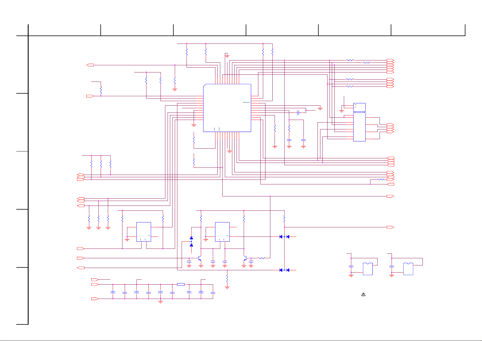
Schematic diagram - MPEG board 1/16
26
Page 25

A B C D E F
PSU_STB
Vcc5V
Vcc3V3
Vcc1V8
Vcc5V Vcc3V3
-12VVcc5V
Vcc12VVcc5VVcc3V3
Vcc12VSTB5V
STB5V -12V
Vcc3V3
J_FIP_FSTB
J_FIP_IR
J_FIP_DATA
J_FIP_CLKO
RESET#
IDE_RESET#
J_FIP_DIN
PSU_STB
PIO_9
Title
Size Document Number
Sigma Designs
355 FairView Way
Milpitas CA 95035
Reference
designs
23-000703-01
Reset / Fip / Power
B
DVD Receiver - EM850
CONFIDENT
Reset
Panel cn
Power Input
1.8V Regulator
3.3V Regulator
DF3-6P-2H(20) HIROSE
DF3-10P-2H(20) HIROSE
74HC04
U11B
3 4
7
14
74HC04
U11D
9 8
7
14
C10210uF/16V
L24
BEAD
L21
Not Mounted
C2000
0.1uF
1 2
R71 10K
L23
BEAD
C2003
0.1uF
1 2
C66 100pF
L46
BEAD
J14
HDR1x2
1
2
C51 100pF
L22
BEAD
C64 100pF
C55 100pF
C176 100pF
C2001
0.1uF
1 2
74HC04
U11E
11 10
7
14
L48
BEAD
C2004
0.1uF
1 2
J41
Conn-RJ-10
1
2
3
4
5
6
7
8
9
10
11
12
74HC04
U11C
5 6
7
14
J40
Conn-RJ-06
1
2
3
4
5
6
7
8
T71
1
T76
1
T73
1
R197 301
T72
1
R195 301
T75
1
Z1
AMS1117 Adj
GND
1
OUT
2
VIN
3
4
4
C123 22pF
R72 10K
R196 130
C124 22pF
R198 510
C50 100pF
C122 22pF
R46 22
L47
BEAD
C13847uF/16V
C121 22pF
C13747uF/16V
T77
1
R11 1K5
C13947uF/16V
T79
1
C152.7nF
T81
1
C120 22pF
R47 22
C12647uF/16V
T78
1
T82
1
L26
BEAD
T80
1
L27
BEAD
L29
BEAD
L28
BEAD
C2247uF/16V
R73
1K
74HC04
U11A
1 2
7
14
74HC04
U11F
13 12
7
14
Z2
AMS1117 Adj
GND1OUT
2
VIN
3
4
4
R70 47K
D12
Dual
2
3
1
T74
1
1
2
3
4
5
Schematic diagram - MPEG board 2/16
Components having special characteristics or critical for safety are
identifi ed by
specifi ed by the manufacturer.
Schematic diagram is subject to change without notice.
mark and must be replaced with components
27
Page 26

A B C D E F
I2CM_SCK
I2CM_SDA
IDE_PD0
IDE_PD1
IDE_PD2
IDE_PD3
IDE_PD4
IDE_PD5
IDE_PD7
IDE_PD6
IDE_PD11
IDE_PD8
IDE_PD10
IDE_PD9
IDE_PD15
IDE_PD13
IDE_PD14
IDE_PD12
IDE_PA0
IDE_PA1
IDE_PA2
I2CM_SCK
I2CM_SDA
I2CM_SCK
I2CM_SDA
I2CM_SDA
PIO_2
PIO_4
PIO_8
PIO_9
PIO_10
PIO_0
PIO_14
PIO_13
PIO_12
PIO_11
VGAEN#
SCT-ENB
SCT-169
I2CM_SCK
Vcc3V3
Vcc3V3
Vcc3V3
Vcc3V3
Vcc3V3
J_FIP_FSTB
J_FIP_DATA
IDE_DIOW#
IDE_DIOR#
IDE_DMARQ
IDE_DACK#
IDE_CS0#
IDE_CS1#
IDE_IRQ
TV_U/B/CVBS
IDE_RDY
TV_Y/G/Y
J_FIP_CLKO
TV_CVBS
TV_V/R/C
IDE_NPCBLID
IDE_PA[2..0]
IDE_PD[15..0]
VSYNC
HSYNC
SPDIFOUT
AUDCLK96
SCT-ENB
SCT-169
J_FIP_DIN
VGAEN#
PIO_10
PIO_11
PIO_9
PIO_4
PIO_8
PIO_2
PIO_0
PIO_13
PIO_14
PIO_12
EM8500_IR_input
PIO_3
EM8500_IR_input
I2C_SDA
I2C_SCL
Title
Size Document Number Re v
Sigma Designs
355 FairView Way
Milpitas CA 95035
Reference
designs
23-000703-01 E6
EM8500
B
DVD Receiver - EM8500
CONFIDENTIAL
HDR1x3
J48
Not Mounted
1
2
3
R337 Not Mounted
R338 Not Mounted
R33500R336
00
R6710K
RP4
4x10K
1823
4
765
RP3
4x10K
1823
4
765
J1
HDR1x3
1
2
3
R602 3K3
24C0x
U2
A0
1
A1
2
A2
3
VSS4SDA
5
SCL
6
WP
7
VCC
8
R6810K
T118
1
T119
1
T120
1
T124
1
T125
1
T126
1
IDE
I2S
FIP
IN-OUT
AUDIO
OUT
TV OUT
VIDEO OUT
I2S
U1A
EM8500
FCLK
V14
FDIN
W13
FDOUT
W14
FSTB
Y13
I2S_SCLK
Y14
I2S_SDATA
T15
I2S_LRCLK
U15
CS0
N16
CS1
Y20
IRQ
R18
IOW
P16
IOR
R17
DMAREQ
T18
ACK
V18
IORDY
U18
NPCBLID
V19
HD_0
W18
HD_1
Y17
HD_2
V17
HD_3
U17
HD_4
V16
HD_5
W16
HD_6
W15
HD_7
V15
HD_8
Y15
HD_9
Y16
HD_10
U16
HD_11
T16
HD_12
T17
HD_13
W17
HD_14
R16
HD_15
Y18
HA_0
Y19
HA_1
P18
HA_2
W19
DVD_CLKIN
P17
PIO1_8
A4
PIO1_7
C8
P23E2P22E3P21F4P20F5P19D3P18E4P17D2P16D1P15C2P14C1P13B1P12E5P11D4P10
D6
P9C3P8B2P7D7P6A2P5B3P4C4P3A1P2C5P1D9P0
A3
PCLK
D5
VSYNC
B4
HSYNC
C6
VVLDC7VCLK
D8
CVBS
J1
Y
H3
U
G1
V
G5
ACLK1
K3
SCOUT1
K2
SDOUT1
M1
SFOUT1
L2
ACLK2
K5
SCOUT2
M5
SDOUT2
J5
SFOUT2
L5
ACLK3
N5
SCOUT3
P6
SDOUT3
R7
SFOUT3
R5
PIO_14
D17
PIO_13
A16
PIO_12
B16
PIO_11
C16
PIO_10
D16
PIO_9
B15
PIO_8
C15
PIO_7
D15
PIO_6
D13
PIO_5
A14
PIO_4
B14
PIO_3
A15
PIO_2
D14
PIO_1
C14
PIO_0
E15
SCIN
K1
DAMCK
J4
DADAT
DABCK
G6
S/PDIF OUT
J3
I2CM_SCLK
U14
I2CM_SDATA
T14
RP2
4x10K
1823
4
765
T69
1
T70
1
T121
1
T122
1
T123
1
T130
1
T129
1
T128
1
T127
1
T131
1
RP27
4x10K
1 823
4
765
R334 Not Mounted
R333 Not Mounted
R601
3K3
1
2
3
4
5
Schematic diagram - MPEG board 3/16
identifi ed by
specifi ed by the manufacturer.
Components having special characteristics or critical for safety are
mark and must be replaced with components
Schematic diagram is subject to change without notice.
28
Page 27

A B C D E F
V_PLL_1V8
XIN XOUT
CLK_OUT
JTAG_TCK
Vcc1V8
Vcc3V3
Vcc1V8
Vcc1V8
Vcc3V3
V_DAC_3V3
Vcc3V3
V_DAC_3V3Vcc3V3
Vcc5V
RESET#
Title
Size Document Number
Sigma Designs
355 FairView Way
Milpitas CA 95035
Reference
designs
23-000703-01
EM8500 Power and decoupling
B
DVD Receiver - EM8500
CONFIDENT
GND
VGND
VGND
Use 200ohm if
single t erminated
C170.1uF
C4110uF/16V
C430.1uF
C420.1uF
C440.1uF
C450.1uF
C360.1uF
C2710uF/16V
C3810uF/16V
C3910uF/16V
C4010uF/16V
C1030.1uF
C240.1uF
C520.1uF
X1
27MHz
1 2
C530.1uF
C130.1uF
R1 1M
1 2
C1 0.1uF
1 2
C310.1uF
C6
27pF
12
L1
BEAD
1 2
C5
27pF
12
R982
C1610uF/16V
C560.1uF
C120.1uF
C570.1uF
PLLs
OSC.
VIDEO
DACs
U1C
EM8500
AVDD_D_33
G4
AVDD_C_33
H5
AVVD_Y_33
H2
AVDD_U_33
G2
AVDD_V_33
F1
RSET
F3
VREF
F2
AVSS_D
E1
CVBS_VSS
J2
YB
H4
UB
H1
VB
G3
VCC_3V3
L1
VSS
K4
RESET#
Y8
PLL_ENABLE
A13
XOUT
A11
XIN
B11
CLK_OUT
B13
TCK
B8
CLK32K
W10
TDO
B7
NTRST
B5
TDI
B6
TMS
A5
SCAN_MODE
Y9
GND
E14
GND
F14
GND
R15
GND
P15
GND
E11
GND
J11
GND
J12
GND
K11
GND
K12
GND
L11
GND
L12
GND
M11
GND
M12
GNDJ9GND
J10
GNDK9GND
K10
GNDL9GND
L10
GNDM9GND
M10
GNDF7GNDT8GNDU8GND
V7
3V3
E12
3V3
E13
3V3
T12
3V3
T13
3V3
T10
3V3
T9
3V3
U9
3V3
U10
3V3
E6
3V3
E7
3V3
E8
3V3
U7
3V3
T7
1V8
K16
1V8
M16
1V8
L16
1V8
D11
1V8
T11
1V8
U11
1V8
V11
1V8
W11
1V8
C9
1V8
C10
1V8
D10
1V8
E9
1V8
E10
1V8
V10
AVDD_P1_18
D12
AVDD_P2_18
A12
AVSS_P1
B12
AVSS_P2
C12
GND
W7
C580.1uF
C600.1uF
C610.1uF
C620.1uF
C1847uF/16V
C320.1uF
C140.1uF
L4
BEAD
1 2
C200.1uF
C1750.1uF
C190.1uF
C230.1uF
C80.1uF
C280.1uF
C1720.1uF
R8 22
1 2
C1060.1uF
T17
1
2
3
4
5
identifi ed by
specifi ed by the manufacturer.
Schematic diagram - MPEG board 4/16
Components having special characteristics or critical for safety are
mark and must be replaced with components
Schematic diagram is subject to change without notice.
29
Page 28

A B C D E F
SYS_MA4
SYS_MA0
SYS_MA1
SYS_MA10
SYS_MA7
SYS_MA5
SYS_MA6
SYS_MA2
SYS_MA8
SYS_MA9
SYS_MA3
SYS_SD_MA11
SYS_SD_BA1
SYS_MA13
SYS_MA12
SYS_SD_BA0
SYS_SD_BA1
SYS_SD_MA11SYS_MA11
SYS_MA11 SYS_SD_BA0
SYS_MA12 SYS_SD_BA0
SYS_SD_DQM0
SYS_SD_DQM1
SYS_SD_DQM2
SYS_SD_DQM3
SYS_SD_CLKEN
SYS_SD_CLK
SYS_MD29
SYS_MD31
SYS_MD1
SYS_MD24
SYS_MD10
SYS_MD14
SYS_MD17
SYS_MD2
SYS_MD26
SYS_MD13
SYS_MD25
SYS_MD8
SYS_MD28
SYS_MD12
SYS_MD27
SYS_MD9
SYS_MD5
SYS_MD4
SYS_MD19
SYS_MD6
SYS_MD16
SYS_MD21
SYS_MD3
SYS_MD7
SYS_MD0
SYS_MD23
SYS_MD30
SYS_MD20
SYS_MD22
SYS_MD18
SYS_MD11
SYS_MD15
SYS_SD_RAS#
SYS_SD_RAS#
SYS_SD_CS#
SYS_FL_WE#
SYS_SD_CLKEN
SYS_SD_CAS#
SYS_SD_CLK_PIN
SYS_MA0
SYS_MA1
SYS_MA2
SYS_MA3
SYS_MA4
SYS_MA5
SYS_MA6
SYS_MA7
SYS_MA8
SYS_MA10
SYS_MA9
SYS_MA11
SYS_MA12
SYS_MA13
SYS_MA14
SYS_MA16
SYS_MA15
SYS_MA17
SYS_MA19
SYS_MD1
SYS_MA18
SYS_MD0
SYS_MA20
SYS_MD2
SYS_MD3
SYS_MD4
SYS_MD6
SYS_MD5
SYS_MD7
SYS_MD9
SYS_MD11
SYS_MD13
SYS_MD8
SYS_MD12
SYS_MD10
SYS_MD22
SYS_MD24
SYS_MD15
SYS_MD23
SYS_MD16
SYS_MD25
SYS_MD17
SYS_MD18
SYS_MD20
SYS_MD19
SYS_MD21
SYS_MD14
SYS_MD29
SYS_MD31
SYS_MD28
SYS_MD27
SYS_MD26
SYS_MD30
SYS_MD[31:0]
SYS_SD_DQM0
SYS_SD_DQM1
SYS_SD_DQM2
SYS_SD_DQM3
SYS_MA[20:0]
SYS_SD_DQM[3:0]
SYS_SD_CS#
SYS_SD_CAS#
SYS_MA[20..0]
SYS_FL_WE#
SYS_FL_BYTE#
PULLUP
A20
SYS_FL_RDY
SYS_FL_CS#_MEM
SYS_SD_WE#
RESET#
SYS_MD8
SYS_MD1
SYS_MD6
SYS_MD10
SYS_MD3
SYS_MD2
SYS_MD0
SYS_MD13
SYS_MD11
SYS_MD5
SYS_MD7
SYS_MD4
SYS_MD12
SYS_MD15
SYS_MD9
SYS_MD14
SYS_MA3
SYS_MA1
SYS_MA7
SYS_MA4
SYS_MA0
SYS_MA14
SYS_MA16
SYS_MA13
SYS_MA6
SYS_MA15
SYS_MA8
SYS_MA5
SYS_MA17
SYS_MA10
SYS_MA11
SYS_MA12
SYS_MA2
SYS_MA18
SYS_MA9
SYS_SD_BA1
FLASH_CFG_0
FLASH_CFG_1
RESET#
SYS_FL_RDY
SYS_FL_BYTE#
PULLUP
A20 SYS_MA20
SYS_MA19
SYS_FLASH_CS#
SYS_FL_CS#
SYS_FL_CS#_MEM
SYS_FL_MEM_WAIT#
SYS_MA19
SYS_MA16
SYS_MA13
SYS_MA0
SYS_MA17
SYS_MA12
SYS_MA7
SYS_MA18
SYS_MA1
SYS_MA11
SYS_MA9
SYS_MA8
SYS_MA10
SYS_MA3
SYS_MA6
SYS_MA15
SYS_MA14
SYS_MA2
SYS_MA4
SYS_MA5
SYS_MD0
SYS_MD14
SYS_MD15
SYS_MD3
SYS_MD12
SYS_MD8
SYS_MD5
SYS_MD7
SYS_MD4
SYS_MD6
SYS_MD10
SYS_MD1
SYS_MD9
SYS_MD13
SYS_MD2
SYS_MD11
RESET#
SYS_FL_BYTE#
SYS_SD_WE#
SYS_FL_CS#_MEM
SYS_SD_WE#
SYS_SD_WE#
SYS_FL_WE#
SYS_FL_RDY
A20
Vcc3V3 Vcc3V3
Vcc3V3
SYS_MD[31:0]
SYS_FL_CS#
SYS_SD_WE#
SYS_FL_WE#
SYS_FL_RDY
RESET#
SYS_MA[20:0]
Title
Size Document Number Re
Sigma Designs
355 FairView Way
Milpitas CA 95035
Reference
designs
23-000703-01
EM8500 Sys SDRAM + Flash
B
DVD Receiver - EM8500
CONFIDENTIA
2Mx32
8MB
4Mx32
16MB
To Flash E mulator
STUFF SYS _MA20 => A20
FOR 2M x 16 CHIP (4MB)
AT49BV32xx
Use Emulator
Use Flash
T38
1
T34
1
T42
1
RP5
4x10K
1823
4
765
T44
1
T36
1
T50
1
T46
1
PO CHK.
U24
MBM29LV320BM
A15
1
A14
2
A13
3
A12
4
A11
5
A10
6
A9
7
A8
8
A19
9
NC
10
WE
11
RESET12NC13NC
14
A18
16
A17
17
A7
18
A6
19
A5
20
A4
21
A3
22
A2
23
A1
24
A0
25
CE
26
GND
27
OE
28
D0
29
D8
30
D1
31
D9
32
D2
33
D10
34
D3
35
D11
36
VCC
37
D4
38
D12
39
D5
40
D13
41
D6
42
D14
43
D7
44
D15
45
GND
46
BYTE
47
A16
48
RDY/BUSY
15
R32 Not Mounted
T51
1
T41
1
T40
1
R33 Not Mounted
T53
1
T23
1
T48
1
R34 Not Mounted
T55
1
T43
1
T19
1
T27
1
T29
1
T54
1
T21
1
T57
1
T45
1
T52
1
R127
Not Mounted
T35
1
T56
1
T31
1
T58
1
T47
1
CHK PO.
U3
4Mx32 MT48LC4M32B2TG-7
DQ0
2
VDDQ
3
DQ1
4
DQ2
5
DQ3
7
DQ4
8
VDDQ
9
DQ5
10
DQ16
31
VSSQ
32
DQ17
33
DQ18
34
DQ19
36
DQ20
37
VSSQ
38
DQ21
39
DQM0
16
WE
17
CAS
18
RAS
19
BA0
22
BA1
23
A10
24
A0
25
A1
26
VDD
15
NC
14
DQM2
28
VDD
29
DQ7
13
A2
27
A11
21
VDDQ
35
DQ22
40
VDD
1
CS
20
VSSQ
6
DQ6
11
VSSQ
12
NC
30
VDDQ
41
DQ23
42
VDD
43
VSS
44
DQ24
45
VSSQ
46
DQ25
47
DQ26
48
VDDQ
49
DQ27
50
DQ28
51
VSSQ
52
DQ29
53
DQ30
54
VDDQ
55
DQ31
56
NC
57
VSS
58
DQM3
59
A3
60
A4
61
A5
62
A6
63
A7
64
A8
65
A9
66
CLKE
67
CLK
68
NC
69
NC
70
DQM1
71
VSS
72
NC
73
DQ8
74
VDDQ
75
DQ9
76
DQ10
77
VSSQ
78
DQ11
79
DQ12
80
VDDQ
81
DQ13
82
DQ14
83
VSSQ
84
DQ15
85
VSS
86
T39
1
T25
1
R129
Not Mounted
T37
1
T49
1
T33
1
T59
1
T26
1
R2810K
R115
00
T28
1
R2910K
T24
1
T30
1
C54
Not Mounted
1 2
T22
1
T20
1
J32
HDR1x3
1
2
3
T18
1
R12510K
T32
1
R10
22
R12610K
R122 00
R30 00
T68
1
U1B
EM8500
MD_31
K17
MD_30
J19
MD_29
K20
MD_28
K19
MD_27
L17
MD_26
M20
MD_25
P20
MD_24
R20
MD_23
N17
MD_22
N20
MD_21
L19
MD_20
L20
MD_19
K18
MD_18
J20
MD_17
H20
MD_16
H19
MD_15
G15
MD_14
F15
MD_13
B17
MD_12
A17
MD_11
A18
MD_10
F17
MD_9
B19
MD_8
A19
MD_7
G16
MD_6
B18
MD_5
D18
MD_4
E17
MD_3
F16
MD_2
C17
MD_1
C18
MD_0
E16
MA_20
M18
MA_19
W20
MA_18
M17
MA_17
N19
MA_16
V20
MA_15
U20
MA_14
T20
MA_13
L18
MA_12
M19
MA_11
G18
MA_10
H17
MA_9
B20
MA_8
C20
MA_7
E19
MA_6
F19
MA_5
J17
MA_4
J16
MA_3
F20
MA_2
E20
MA_1
D20
MA_0
G19
DQM0
E18
DQM1
G17
DQM2
J18
DQM3
G20
SDRAM_WE# / FLASH_OE#
D19
SDRAM_CS#
A20
SDRAM_RAS#
F18
SDRAM_CAS#
H16
SDRAM_CLK
C19
SDRAM_CLKEN
H18
FLASH_WE#
T19
FLASH_CS#
U19
MEM_WAIT#
P19
FLASH_CFG_0
N18
FLASH_CFG_1
R19
R31 00
1
2
3
4
5
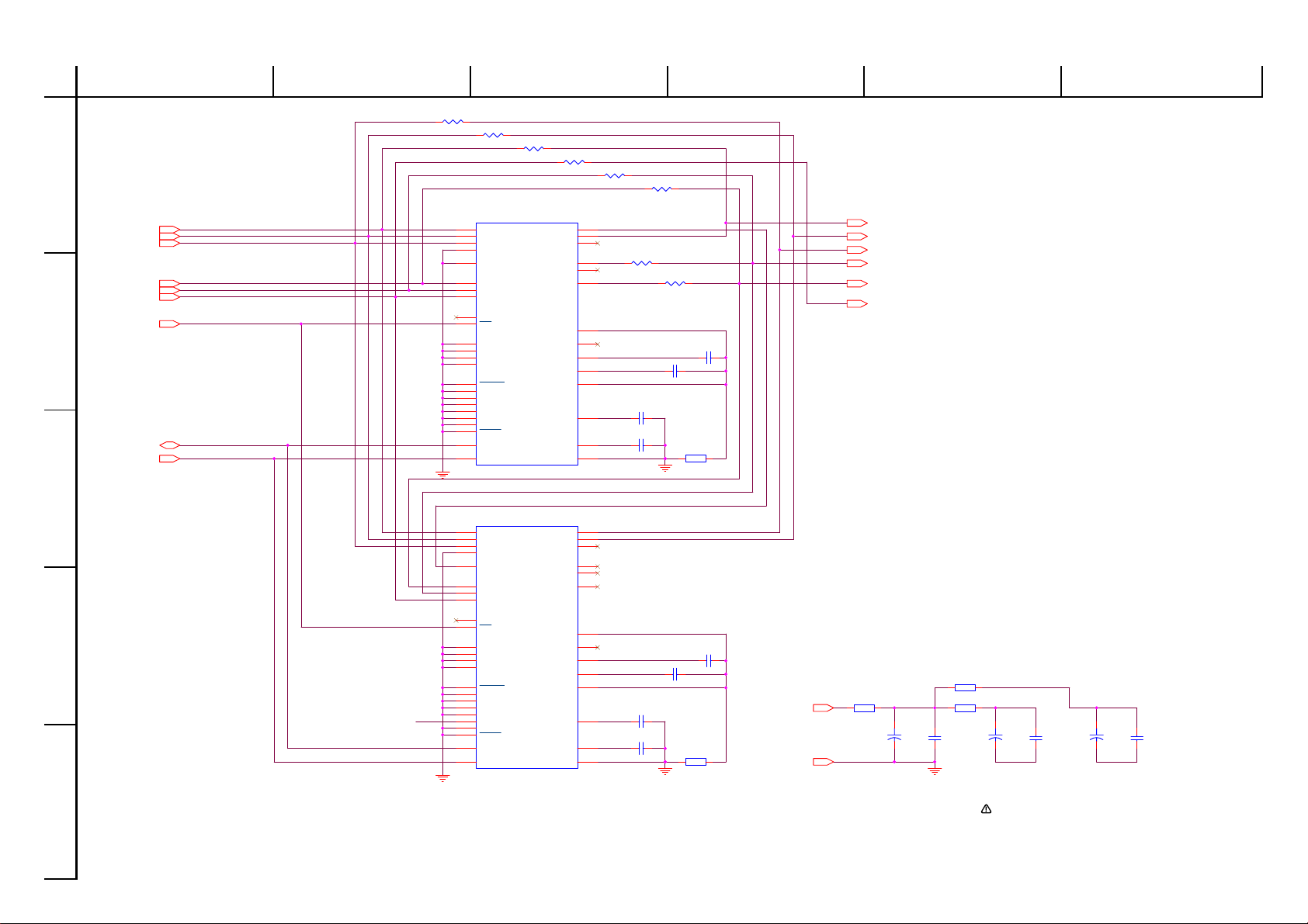
Schematic diagram - MPEG board 5/16
Components having special characteristics or critical for safety are
identifi ed by
specifi ed by the manufacturer.
Schematic diagram is subject to change without notice.
mark and must be replaced with components
30
Page 29

A B C D E F
MPG_SD_D[31:0]
1
2
3
MPG_SD_D31
MPG_SD_D30
MPG_SD_D29
MPG_SD_D28
MPG_SD_D27
MPG_SD_D26
MPG_SD_D25
MPG_SD_D24
MPG_SD_D23
MPG_SD_D22
MPG_SD_D21
MPG_SD_D20
MPG_SD_D19
MPG_SD_D18
MPG_SD_D17
MPG_SD_D16
MPG_SD_D0
MPG_SD_D1
MPG_SD_D2
MPG_SD_D3
MPG_SD_D4
MPG_SD_D5
MPG_SD_D6
MPG_SD_D7
MPG_SD_D8
MPG_SD_D9
MPG_SD_D10
MPG_SD_D11
MPG_SD_D12
MPG_SD_D13
MPG_SD_D14
MPG_SD_D15
R27 10K
R26 Not Mounted
1
2
3
4 5
1
2
3
4 5
R21 Not Mounted
R20 10K
R23 Not Mounted
R22 10K
R25 Not Mounted
R24 10K
R65 Not Mounted
R66 10K
R93 Not Mounted
R77 10K
R94 10K
R78 Not Mounted
R95 10K
R79 Not Mounted
R96 10K
R64 Not Mounted
4 5
3
2
1
4 5
3
2
1
4 5
3
2
1
4 5
3
2
1
4
Vcc3V3
6-Ch
2-Ch
8
RP25
7
4x10K
6
8
RP23
7
4x10K
6
RP19
6
4x10K
7
8
RP18
6
4x10K
7
8
RP21
6
4x10K
7
8
RP20
6
4x10K
7
8
SCART (Europe)
no DVI
I2S OUT
Reserved
ID
J_UART1_DTR
J_UART1_DSR
J_UART1_RTS
J_UART1_CTS
J_UART1_RXD
J_UART1_RI
J_UART1_CD
J_UART1_TXD
B10
A10
C11
C13
Y12
Y11
V12
V13
Y10
U12
U13
W12
U1D
MPG_SD_D31
MM_CS#
MM_WE#
MM_CAS#
MM_RAS#
MM_CLK
W8
W6
V6
Y5
V5
Y4
W4
V8
W3
Y2
Y3
U5
W5
Y6
U6
T6
V4
T5
U4
F6
T3
N4
U2
R3
T2
W2
V2
U3
P4
R4
T4
R6
P2
T1
M3
R1
L3
M2
H6
L4
M4
N1
P1
N2
R2
V1
Y1
P5
V3
W1
N3
P3
U1
MPG_SD_D30
MPG_SD_D29
MPG_SD_D28
MPG_SD_D27
MPG_SD_D26
MPG_SD_D25
MPG_SD_D24
MPG_SD_D23
MPG_SD_D21
MPG_SD_D20
MPG_SD_D19
MPG_SD_D18
MPG_SD_D17
MPG_SD_D16
MPG_SD_D15
MPG_SD_D14
MPG_SD_D13
MPG_SD_D12
MPG_SD_D11
MPG_SD_D10
MPG_SD_D9
MPG_SD_D8
MPG_SD_D7
MPG_SD_D6
MPG_SD_D5
MPG_SD_D4
MPG_SD_D3
MPG_SD_D1
MPG_SD_D0
MPG_SD_A11
MPG_SD_A10
MPG_SD_A9
MPG_SD_A8
MPG_SD_A7
MPG_SD_A6
MPG_SD_A5
MPG_SD_A4
MPG_SD_A3
MPG_SD_A2
MPG_SD_A1
MPG_SD_A0
R6322
MPG_SD_DQM0
MPG_SD_DQM1
MPG_SD_DQM2
MPG_SD_DQM3
MM_DATA31
MM_DATA30
MM_DATA29
MM_DATA28
MM_DATA27
MM_DATA26
MM_DATA25
MM_DATA24
MM_DATA23
MM_DATA22
MM_DATA21
MM_DATA20
MM_DATA19
MM_DATA18
MM_DATA17
MM_DATA16
MM_DATA15
MM_DATA14
Y7
NC
V9
NC
W9
NC
EM8500
A7
DTRN0
DSRN0
B9
RTSN0
A9
RIN0
CTSN0
DCDN0
A6
TXD0
A8
RXD0
UCLK0
DSRN1
DCDN1
DTRN1
RTSN1
CTSN1
RXD1
TXD1
RIN1
MM_DATA13
MM_DATA12
MM_DATA11
MM_DATA10
MM_DATA9
MM_DATA8
MM_DATA7
MM_DATA6
MM_DATA5
MM_DATA4
MM_DATA3
MM_DATA2
MM_DATA1
MM_DATA0
MM_ADD_11/BA
MM_ADD_10
MM_ADD_9
MM_ADD_8
MM_ADD_7
MM_ADD_6
MM_ADD_5
MM_ADD_4
MM_ADD_3
MM_ADD_2
MM_ADD_1
MM_ADD_0
MM_DQM_0
MM_DQM_1
MM_DQM_2
MM_DQM_3
MPG_SD_A[11:0]
MPG_SD_DQM[3:0]
Vcc3V3
MPG_SD_A11
MPG_SD_A10
MPG_SD_A9
MPG_SD_A8
MPG_SD_A7
MPG_SD_A6
MPG_SD_A5
MPG_SD_A4
MPG_SD_A3
MPG_SD_A2
MPG_SD_A1
MPG_SD_A0
MPG_SD_CS#
MPG_SD_WE#
MPG_SD_CAS#
MPG_SD_RAS#
MPG_SD_CLK
MPG_SD_DQM0
MPG_SD_DQM1
MPG_SD_DQM2
MPG_SD_DQM3
23
22
24
66
65
64
63
62
61
60
27
26
25
20
17
18
19
67
68
16
71
28
59
14
21
30
73
70
69
57
Vcc3V3
BA1
BA0
A10
A9
A8
A7
A6
A5
A4
A3
A2
A1
A0
CS
WE
CAS
RAS
CLKE
CLK
DQM0
DQM1
DQM2
DQM3
NC
NC
NC
NC
NC
NC
NC
1
VDD
VSS
44
3
9
35
15
VDD
KM432S2030CT-G8
VSS
58
41
29
43
VDD
VDD
VDDQ
VDDQ
VDDQ
VDDQ
U4
VSSQ
VSSQ
VSSQ
VSSQ
VSS
VSS
6
32
38
12
72
86
49
VDDQ
VSSQ
46
55
VDDQ
VSSQ
52
75
VDDQ
VSSQ
78
81
VDDQ
DQ31
DQ30
DQ29
DQ28
DQ27
DQ26
DQ25
DQ24
DQ23
DQ22
DQ21
DQ20
DQ19
DQ18
DQ17
DQ16
DQ15
DQ14
DQ13
DQ12
DQ11
DQ10
DQ9
DQ8
DQ7
DQ6
DQ5
DQ4
DQ3
DQ2
DQ1
DQ0
VSSQ
84
56
54
53
51
50
48
47
45
42
40
39
37
36
34
33
31
85
83
82
80
79
77
76
74
13
11
10
8
7
5
4
2
MPG_SD_D31
MPG_SD_D30
MPG_SD_D29
MPG_SD_D28
MPG_SD_D27
MPG_SD_D26
MPG_SD_D25
MPG_SD_D24
MPG_SD_D23
MPG_SD_D22MPG_SD_D22
MPG_SD_D21
MPG_SD_D20
MPG_SD_D19
MPG_SD_D18
MPG_SD_D17
MPG_SD_D16
MPG_SD_D15
MPG_SD_D14
MPG_SD_D13
MPG_SD_D12
MPG_SD_D11
MPG_SD_D10
MPG_SD_D9
MPG_SD_D8
MPG_SD_D7
MPG_SD_D6
MPG_SD_D5
MPG_SD_D4
MPG_SD_D3
MPG_SD_D2MPG_SD_D2
MPG_SD_D1
MPG_SD_D0
Components having special characteristics or critical for safety are
identifi ed by
5
specifi ed by the manufacturer.
Schematic diagram is subject to change without notice.
Schematic diagram - MPEG board 6/16
mark and must be replaced with components
31
Page 30

A B C D E F
1
IDE_RESET#
T83
1
2
3
4
IDE_PD[15..0]
IDE_PA[2..0]
IDE_IRQ
IDE_DIOR#
IDE_DIOW#
IDE_RDY
IDE_CS0#
IDE_CS1#
IDE_DMARQ
IDE_DACK#
IDE_NPCBLID
Vcc12V
IDE_PD15
IDE_PD14
IDE_PD13
IDE_PD12
IDE_PD11
IDE_PD10
IDE_PD9
IDE_PD8
IDE_PD7
IDE_PD6
IDE_PD5
IDE_PD4
IDE_PD3
IDE_PD2
IDE_PD1
IDE_PD0
IDE_PA2
IDE_PA1
IDE_PA0
IDE_IRQ
IDE_DIOR#
IDE_DIOW#
IDE_RDY
IDE_CS0#
IDE_CS1#
IDE_DMARQ
IDE_DACK#
IDE_NPCBLID
1
T99
1
T98
1
T97
1
T96
1
T95
1
T94
1
T93
1
T92
1
T91
1
T90
1
T89
1
T88
1
T87
1
T86
1
T85
1
T84
1
T102
1
T101
1
T100
1
T110
1
T111
1
T103
1
T108
1
T104
1
T105
1
T109
1
T107
1
T106
1
T112
1
T113
1
T114
1
T115
1
T116
1
T117
Vcc3V3
Vcc3V3
Vcc3V3
R116
Not Mounted
4K7 if mounted
R105 10K
R106 10K
R199 1K
R108 Not Mounted
10K if mounted
R109 10K
IDE_DIOW#
IDE CONNECTOR
IDE_PD7
IDE_DMARQ
IDE_RDY
IDE_IRQ IDE_CS0#
IDE_RESET#
IDE_PD7
IDE_PD6
IDE_PD5
IDE_PD4
IDE_PD3
IDE_PD2
IDE_PD1
IDE_PD0
IDE_DMARQ
IDE_DIOW#
IDE_DIOR#
IDE_RDY
IDE_DACK#
IDE_IRQ
IDE_PA1
IDE_PA0
J20
1 2
3 4
5 6
7 8
9 10
11 12
13 14
15 16
17 18
19 20
21 22
23 24
25 26
27 28
29 30
31 32
33 34
35 36
37 38
39 40
IDE
GNDGND
KEY
reserved
GND
IDE_PD8
IDE_PD9
IDE_PD10
IDE_PD11
IDE_PD12
IDE_PD13
IDE_PD14
IDE_PD15
IDE_N PCBLID
IDE_PA2
IDE_CS1#
12
C167
0.1uF
R114
5
GND
Not Mounted
4K7 if mounted
IDE_CS1#
Schematic diagram - MPEG board 7/16
Components having special characteristics or critical for safety are
identifi ed by
mark and must be replaced with components
specifi ed by the manufacturer.
Schematic diagram is subject to change without notice.
32
Page 31

A B C D E F
SCT-V8
SCT-V16
VGAHSHSYNC
TV_V/R/C C-Pr
VBS-YTV_Y/G/Y
PbTV_U/B/CVBS
VGA-ENB
VGA-ENB
SCART-G
S-Vid-C/Pr
S-Vid-Y/Y
S-Vid-C/Pr
VBS-Y
VBS-Y
C-Pr
CVBS_out
C-Pr
SCART-B
SCART-CVBS
SCART-G
SCART-G
SCART-R
SCART-R
Composite
S-Vid-Y/Y
SCART-B
SCART-B
TV_V/R/C
TV_Y/G/Y
TV_U/B/CVBS
SCART-CVBS
CVBS_out
Pb
Pb SCART-B
S-Vid/Pb
S-Vid/Pb
VGAVS
VGA-ENB
VGA-ENB
VSYNC
SCART-R
SCART-R
SCART-G
Vcc12V Vcc12V
Vcc3V3
Vcc5V Vcc5V
Vcc12V
Vcc3V3
Vcc3V3
Vcc5V
Vcc5V
Vcc3V3
HSYNC
VSYNC
SCT-ENB
SCT-169
VGAEN#
TV_U/B/CVBS
TV_Y/G/Y
SCT-ENB
TV_V/R/C
TV_CVBS
S-Vid-C/Pr
S-Vid-Y/Y
S-Vid/Pb
Composite
SCART-CLK
SCART-DATA
SCART-CVBS
SCART-R
SCART-G
SCART-B
SCART-V8
SCART-V16
Title
Size Document Number R ev
Date: Sheet of
Sigma Designs
355 FairView Way
Milpitas CA 95035
Reference
designs
23-000703-01 E 6
Video Out
B
816Tuesday, July 15, 2003
DVD Receiver - EM8500
CONFIDENTIAL
CONFIDENTIAL
For VGA output
Optional By-pass filter
for VGA output
Optional By-pass
Mux U39
No Stuff for Single termination
Alternate
HDTV/S-VIDEO
BSS138
BSS138
BSS138
DATA
CLKOUT
D17
Dual
2
3
1
74LCX125
U21B
5 6
7
14
4
74LCX125
U21A
2 3
7
14
1
R51
4K7
R431K
Q11
2N3906
1
3 2
R44
1K
R4847
Q8
2N3904
1
32
R9975
R52
3K9
R421K
C80330pF
C79330pF
R84 Not Mounted
C78330pF
U39
PI5V330
S1A
2
S2A
3
DA
4
S1B
5
S2B
6
DB
7
S1C
11
S2C
10
DC
9
S1D
14
S2D
13
DD
12
VDD
16
GND
8
EN
15
IN1/IN2
1
C77330pF
Q16
Not Mounted
1
23
R5975
Q17
Not Mounted
1
23
R6075
Q18
Not Mounted
1
23
R6175
Q19
2N3904
1
32
R6275
Q23
2N3906
1
3 2
L12
1.8uH
R9775
C7422pF
U41
PI5V330
S1A
2
S2A
3
DA
4
S1B
5
S2B
6
DB
7
S1C
11
S2C
10
DC
9
S1D
14
S2D
13
DD
12
VDD
16
GND
8
EN
15
IN1/IN2
1
C7522pF
R371K
L5
1.8uH
R351K
L7
1.8uH
R694K7
R3822
C7622pF
D14
Dual
2
3
1
D13
Dual
2
3
1
L11
1.8uH
R3622
C7322pF
U40B
74ACT125
B35O3
6
A3
4
VDD
14
GND
7
U40A
74ACT125
B32O3
3
A3
1
VDD
14
GND
7
R401K
R53
4K7
R451K
R80 Not Mounted
R81 Not Mounted
R82 Not Mounted
D4
Dual
2
3
1
Q22
2N3904
1
32
D1
Dual
2
3
1
R83 Not Mounted
D2
Dual
2
3
1
Q24
2N3904
1
32
D3
Dual
2
3
1
R9875
Q9
2N3904
1
32
74LCX125
U21C
12 11
7
14
13
Q10
2N3904
1
32
74LCX125
U21D
9 8
7
14
10
R200 Not M ounted
D18
Dual
2
3
1
D15
Dual
2
3
1
D16
Dual
2
3
1
1
2
3
4
5
Schematic diagram - MPEG board 8/16
identifi ed by
specifi ed by the manufacturer.
Components having special characteristics or critical for safety are
Schematic diagram is subject to change without notice.
mark and must be replaced with components
33
Page 32

A B C D E F
AUDIO-L-OUT
AUDIO-R-OUT
AUDIO-L-OUT
AUDIO -OUT-GND
AUDIO -OUT-GND
VA+
VA-
VA+
VA-
AUDIO-R-OUT
AUDIO -OUT-GND
VA+
VA-
Vcc12V
-12V
S-Vid-C/Pr
S-Vid-Y/Y
S-Vid/Pb
Composite
VCR-L-IN
VCR-R-IN
AUX-L-IN
AUX-R-IN
TUNER-IN-L
TUNER-IN-R
S-Vid-Y/Y
S-Vid-C/Pr
AUDIO-R
AUDIO-GND
AUDIO-L
SCART-L-OUT
SCART-R-OUT
SCART-A-GND
Title
Size Document Number R e
Date: Sheet of
s
355 FairView Way
Milpitas CA 95035
Reference
designs
23-000703-01
Audio In + Audio Out + HDTV
B
916Tuesday, July 15, 2003
DVD Receiver - EM8500
CONFIDENTIA
ANALOG AUDIO OUT
S-Video
Composite
Component
GREEN
BLUE
RED
R347 4K7
C218
330pF
C217
1nF
J42
RCA+SVideo
3
4
75896
1
2
J35
RCA3x4
1
1
2
2
3
3
4
4
5
5
6
6
GND
9
GND
10
GND
11
7
7
GND
12
8
8
-
+
U52B
LM833/SO
5
6
7
84
R356 47
R355 47
C179100pF
R341
4K7
R350 560
L111
BEAD
R354
Not Mounted
C309 100pF
C180100pF
L64
BEAD
+
C310
47uF/16V
R342 4K7
C181100pF
-
+
U52A
LM833/SO
3
2
1
84
L69
BEAD
R344 4K7
R353 Not Mounted
L110
BEAD
C182100pF
L88
BEAD
L70
BEAD
L500
BEAD
C219
1nF
C183100pF
R349 560
+
C312
47uF/16V
R
G
B
J44
Stacked RCA
1
2
3
4
5
C307 100pF
L501
BEAD
C308
100pF
R348 4K7
C220
330pF
R351 Not Mounted
C313
0.1uF
R352 Not Mounted
L502
BEAD
L112
BEAD
L71
BEAD
R346 4K7
C306
100pF
R343 4K7
L89
BEAD
L65
BEAD
C184100pF
R345
4K7
C311
0.1uF
L66
BEAD
1
2
3
4
5
Schematic diagram - MPEG board 9/16
Components having special characteristics or critical for safety are
identifi ed by
specifi ed by the manufacturer.
Schematic diagram is subject to change without notice.
mark and must be replaced with components
34
Page 33

A B C D E F
SCART-L-OUT
SCART-R-OUT
SCART-CLK
SCART-V8
SCART-V16
SCART-CVBS
SCART-R
SCART-G
SCART-B
SCART-DATA
SCART-A-GND
SCART-L-IN
SCART-R-IN
Title
Sigma Designs
355 FairView Way
Milpitas CA 95035
Reference
designs
DVD Rec
Existing pad for a PCB edge mounted ground clip.
New Pad for a PCB edge mounted ground clip in the corner of the PCB.
Connect SCART Ground plane here!
L109
BEAD
L53
BEAD
J38
PAD
1
C107100pF
L49
BEAD
J39
PAD
1
C110
100pF
L54
BEAD
C108100pF
C1011nF
C117
100pF
J34
Single SCART
Aud OUT R
1
Aud IN R
2
Aud OUT L
3
Aud IN L
6
B GND
5
AGND
4
B
7
G
11
R
15
R GND
13
G GND
9
CVBS
19
CVBS GND
17
GND
21
GND
18
CVBS IN
20
BLNK
16
GND
14
SWTCH
8
CLKOUT
10
DATA
12
L42
BEAD
L50
BEAD
C115
100pF
L108
BEAD
L51
BEAD
L43
BEAD
C109
100pF
C94100pF
C93100pF
C116
100pF
L52
BEAD
C95100pF
C104
100pF
L106
BEAD
C177
100pF
C97100pF
C105
100pF
L105
BEAD
L107
BEAD
C112
100pF
C178
100pF
C98100pF
L9
BEAD
C113
100pF
C111
100pF
C99100pF
C114
100pF
L63
BEAD
1
2
3
4
5
Components having special characteristics or critical for safety are
identifi ed by
mark and must be replaced with components
specifi ed by the manufacturer.
Schematic diagram - MPEG board 10/16
Schematic diagram is subject to change without notice.
35
Page 34

A B C D E F
J
J
J
Vcc5V
1
1 2
C125 10uF/16V
1 2
C129 0.1uF
GND
U17
2
12
2
Vcc5V
1 2
J_UART1_DTR
_UART1_RTS
J_U ART1_TXD
_UART1_RXD
3
_UART1_CTS
_UART1_DSR
J_UART1_CD
J_UART1_RI
C135 0. 1uF
C132
0.1uF
J_UART1_DTR
J_UART1_RTS
J_UART1_TXD
J_UART1_RXD
J_UART1_CTS
J_UART1_DSR
J_UART1_CD
J_UART1_RI
U1_DTR
U1_TXD
U1_RXD
U1_CD
Vcc5V
C1+
4
C1-
1
V+
3
VCC
23
SHTDN
7
DI1
8
DI2
9
DI3
10
RO1
11
RO2
12
RO3
13
RO4
14
RO5
DS14C535
C2+
C2-
GND
GND
DO1
DO2
DO3
RI1
RI2
RI3
RI4
RI5
V-
28
26
25
5
27
22
21
20
19
18
17
16
15
C131
1 2
0.1uF
1 2
C136 0.1uF
U1_DTR
U1_RTS
U1_TXD
U1_RXD
U1_CTS
U1_DSR
U1_CD
U1_RI
GND
J_UART1_DTR
J_UART1_RTS
J_UART1_TXD
J_UART1_RXD
J_UART1_CTS
J_UART1_DSR
J_UART1_CD
J_UART1_RI
1
T60
1
T61
1
T62
1
T63
1
T64
1
T65
1
T66
1
T67
For Software development only
4
10
case
J18
5
2
3
4
1
TxD
DTR
GND
GND
UART1
CD
RxD
DSR6CTS8RI9RTS
case
7
11
U1_DSR
5
U1_RTS
U1_CTS
U1_RI
GND
Schematic diagram - MPEG board 11/16
Components having special characteristics or critical for safety are
identifi ed by
mark and must be replaced with components
specifi ed by the manufacturer.
Schematic diagram is subject to change without notice.
36
Page 35

A B C D E F
FLEX_MD5
FLEX_MD2
FLEX_MD6
FLEX_MD0
FLEX_MD1
FLEX_SD_WE#
FLEX_MD3
FLEX_MD4
FLEX_MD8
FLEX_MD9
FLEX_MD10
FLEX_MD14
FLEX_MD13
FLEX_MD12
FLEX_MD11
FLEX_MD15
FLEX_FL_CS#
FLEX_MA17
FLEX_MA0
FLEX_MA1
FLEX_MA2
FLEX_MA3
FLEX_MA4
FLEX_MA5
FLEX_MA6
FLEX_MA7
FLEX_MA15
FLEX_FL_WE#
FLEX_MA16
FLEX_MA9
FLEX_MA10
FLEX_MA8FLEX_MD7
FLEX_MA20
FLEX_MA19
FLEX_MA18
FLEX_MA17
FLEX_RDY
FLEX_RST#
FLEX_MA11
FLEX_MA12
FLEX_MA13
FLEX_MA14
FLEX_MD0
FLEX_MD1
FLEX_MD2
FLEX_MD3
FLEX_MD4
FLEX_MD5
FLEX_MD6
FLEX_MD7
FLEX_MD8
FLEX_MD9
FLEX_MD10
FLEX_MD11
FLEX_MD12
FLEX_MD13
FLEX_MD14
FLEX_MD15
SYS_MD2
SYS_MD3
SYS_MD7
SYS_MD0
SYS_MD1
SYS_MD6
SYS_MD4
SYS_MD5
SYS_MD12
SYS_MD14
SYS_MD9
SYS_MD15
SYS_MD13
SYS_MD10
SYS_MD8
SYS_MD11
FLEX_MA20
FLEX_FL_CS#
FLEX_FL_CS#
FLEX_FL_WE#
FLEX_MA18
FLEX_MA16
FLEX_MA17
FLEX_MA19
FLEX_SD_WE#
FLEX_MA0
FLEX_MA1
FLEX_MA2
FLEX_MA3
FLEX_MA4
FLEX_MA5
FLEX_MA6
FLEX_MA7
FLEX_MA8
FLEX_MA9
FLEX_MA10
FLEX_MA11
FLEX_MA12
FLEX_MA15
FLEX_MA14
FLEX_MA13
FLEX_RST#
FLEX_RDY
FLEX_FL_WE#
SYS_MA16
SYS_MA17
SYS_MA18
SYS_MA19
SYS_MA0
SYS_MA1
SYS_MA2
SYS_MA3
SYS_MA4
SYS_MA5
SYS_MA6
SYS_MA7
SYS_MA10
SYS_MA11
SYS_MA12
SYS_MA13
SYS_MA14
SYS_MA15
SYS_MA20
SYS_MA8
SYS_MA9
Vcc5V
Vcc3V3
Vcc3V3
Vcc3V3
Vcc3V3
Vcc3V3
Vcc3V3
SYS_MA[20:0]
SYS_FL_WE#
SYS_SD_WE#
SYS_FL_CS#
RESET#
SYS_MD[31:0]
SYS_FL_RDY
Title
Size Document Number
Sigma Designs
355 FairView Way
Milpitas CA 95035
Reference
designs
23-000703-01
(Debug) Flash Emulator
B
DVD Re
FlexROM III
For Software development only
FIDUCIAL
74LVX245
U32
DIR
1
B8
11
A2
3
A3
4
A6
7
A7
8
B6
13
B5
14
B2
17
B118A1
2
A4
5
A5
6
A8
9
B7
12
B4
15
B3
16
G
19
VDD
20
GND
10
74LVX245
U36
DIR
1
B8
11
A2
3
A3
4
A6
7
A7
8
B6
13
B5
14
B2
17
B118A1
2
A4
5
A5
6
A8
9
B7
12
B4
15
B3
16
G
19
VDD
20
GND
10
74LVX245
U35
DIR
1
B8
11
A2
3
A3
4
A6
7
A7
8
B6
13
B5
14
B2
17
B118A1
2
A4
5
A5
6
A8
9
B7
12
B4
15
B3
16
G
19
VDD
20
GND
10
74LVX245
U33
DIR
1
B8
11
A2
3
A3
4
A6
7
A7
8
B6
13
B5
14
B2
17
B118A1
2
A4
5
A5
6
A8
9
B7
12
B4
15
B3
16
G
19
VDD
20
GND
10
J31
HDR2x8
12
34
56
78
910
1112
1314
1516
74LVX245
U34
DIR
1
B8
11
A2
3
A3
4
A6
7
A7
8
B6
13
B5
14
B2
17
B118A1
2
A4
5
A5
6
A8
9
B7
12
B4
15
B3
16
G
19
VDD
20
GND
10
J30
HDR 2x20 MALE
12
34
56
78
910
1112
1314
1516
1718
1920
2122
2324
2526
2728
2930
3132
3334
3536
3738
3940
M38
1
M5
1
M37
1
M35
1
M32
1
M34
1
M36
1
74LCX125
U37A
2 3
7
14
1
74LCX125
U37B
5 6
7
14
4
74LCX125
U37D
9 8
7
14
10
74LCX125
U37C
12 11
7
14
13
1
2
3
4
5
Schematic diagram - MPEG board 12/16
Components having special characteristics or critical for safety are
identifi ed by
specifi ed by the manufacturer.
Schematic diagram is subject to change without notice.
mark and must be replaced with components
37
Page 36

A B C D E F
VCC3V3
VCC3V3
VCC3V3
VCC3V3
VCC3V3
VCC3V3
VCC3V3
VCC3V3
I2C_SCL
I2C_SDA
PIO_12
PIO_13
PIO_14
AUDCLK96
SPDIFOUT
TUN_OUTL
TUN_OUTR
DSP1_PIN2
Sigma Designs
355 FairView Way
Milpitas CA 95035
Reference
designs
DVD Receiver - EM8500
CONFIDENT
DSP Interface 1
From Tuner Interface
Neltron P/N
1224SM-24-30
PCB to
FFC/FPC
Connector
PIO1_7
PIO1_8
L2001
BEAD
C196
Not Mounted
C195
Not Mounted
L77
BEAD
L76
BEAD
L2002
BEAD
C194
100pF
C193
100pF
C188
Not Mounted
C187
Not Mounted
DSP1
FPC-24
A1
A2
A3
A4
A5
A6
A7
A8
A9
A10
A11
A12
A13
A14
A15
A16
A17
A18
A19
A20
A21
A22
A23
A24
B1
B2
B3
B4
B5
B6
B7
B8
B9
B10
B11
B12
B13
B14
B15
B16
B17
B18
B19
B20
B21
B22
B23
B24
L73
BEAD
L81
BEAD
C204
100pF
C203
100pF
R201
10K
L2000
BEAD
R202
10K
L74
BEAD
C186
Not Mounted
R203
10K
C185
Not Mounted
L72
BEAD
C190
100pF
C189
100pF
L75
BEAD
C192
100pF
C191
100pF
L78
BEAD
D19
Dual
2
3
1
D21
Dual
2
3
1
D20
Dual
2
3
1
D22
Dual
2
3
1
D23
Dual
2
3
1
D24
Dual
2
3
1
D28
Dual
2
3
1
1
2
3
4
5
mark and must be replaced with components
Components having special characteristics or critical for safety are
identifi ed by
specifi ed by the manufacturer.
Schematic diagram is subject to change without notice.
Schematic diagram - MPEG board 13/16
38
Page 37

A B C D E F
OPTICAL-IN
COAXIAL-IN
VCR-L
OPTICAL-OUT
TV-IN-L
AUX-R
AUDIO-R
AUDIO-L
AUX-L
VCR-R
AUDIO-GND
VCC5V
VCC5V
VCR-L-IN
VCR-r-IN
AUX-L-IN
AUX-R-IN
SCART-L-IN
TUNER-IN-L
TUNER-IN-R
SCART-R-IN
AUDIO-L
AUDIO-R
AUDIO-GND
Title
Sigma Designs
355 FairView Way
Milpitas CA 95035
Reference
designs
DVD R
LFE Output
VCR Input
S/PDIF Optical output
Auxiliary Input
S/PDIF Optical input
S/PDIF Coaxial input
DSP Interface 2
FROM SCART
RCA TV INPUT
Neltron P/N
1224SM-24-30
PCB to
FFC/FPC
Connector
Place these components
close to J35
Downmix Output
Page 9
Place filter components near DSP2 interface
L506
BEAD
C230
22nF
C235
100pF
L94
BEAD
C224
3.3nF
L86
BEAD
C223
22nF
C222
3.3nF
L507
BEAD
C233
22pF
C216
3.3nF
L503
BEAD
L90 680
C215
22nF
C211
22nF
L87 680
C214
22pF
C229
0.1uF
L91 680
C212
3.3nF
L85 680
C234
22nF
L96
BEAD
C213
22pF
L508
BEAD
C221
22nF
C231
100pF
DSP2
FPC-24
A1
A2
A3
A4
A5
A6
A7
A8
A9
A10
A11
A12
A13
A14
A15
A16
A17
A18
A19
A20
A21
A22
A23
A24
B1
B2
B3
B4
B5
B6
B7
B8
B9
B10
B11
B12
B13
B14
B15
B16
B17
B18
B19
B20
B21
B22
B23
B24
C232
22pF
C236
0.1UF
L95
BEAD
L93 680
L92 680
C225
22nF
C227
22nF
C226
3.3nF
C228
3.3nF
J37
RCA1x1 Blue
1
2
J47
RCA1x1 Orange
1
2
J36
GP1FA 550TZ
VCC
2
GND
3
Vin
1
J46
GP1FA550RZ
GND
2
VOUT
3
VCC
1
L509
BEAD
L504
BEAD
L505
BEAD
1
2
3
4
5
identifi ed by
specifi ed by the manufacturer.
Schematic diagram - MPEG board 14/16
Components having special characteristics or critical for safety are
mark and must be replaced with components
Schematic diagram is subject to change without notice.
39
Page 38

A B C D E F
TUN_RDSDATA
TUN_RDSCLK
TUN_ST
TUN_CE
TUN_DATAIN
TUN_CLK
TUN_DATAOUT
TUN_Ok
TUN_Ok
TUN_ST
TUN_CE
TUN_RDSCLK
TUN_CLK
TUN_DATAOUT
TUN_RDSDATA
TUN_DATAIN
VCC5V
VCC5V Vcc3V3
VCC5V
VCC3V3
VCC5V VCC5V
VCC3V3
VCC3V3
VCC5VVCC5V VCC3V3
VCC5V
VCC5V
VCC3V3
VCC3V3
VCC5V
VCC5V
VCC5V
VCC5V
VCC5V
VCC5V
VCC5V
Vcc12V
PIO_11
PIO_10
PIO_8
PIO_4
PIO_2
PIO_4
PIO_10
PIO_4
PIO_4
PIO_11
PIO_4
PIO_0
TUN_OUTL
TUN_OUTR
PIO_8
DSP1_PIN2
Title
Size Document Number
Date: Sheet
Sigma Designs
355 FairView Way
Milpitas CA 95035
Reference
designs
23-000703-01
FM Tuner Interface
B
15Tuesday, July 15, 2003
DVD Receiver - EM
CONF
RDS
Interface
Status Interface
Tuner Interface
To DSP
Interface 1
PIO4 = Lo -> Tuner Control
PIO4 = Hi -> Read RDS & ST
Q30
2N3904
1
32
L99
BEAD
C243
100pF
C244
100pF
L102
BEAD
C249
100pF
C250
100pF
U47C
74LCX125
B312O3
11
A3
13
VDD
14
GND
7
U47A
74LCX125
B32O3
3
A3
1
VDD
14
GND
7
D37
Dual
2
3
1
D34
Dual
2
3
1
R340
4R7
C242
100pF
L98
BEAD
C241
100pF
D33
Dual
2
3
1
U51B
74LCX125
B35O3
6
A3
4
VDD
14
GND
7
U51C
74LCX125
B312O3
11
A3
13
VDD
14
GND
7
U51D
74LCX125
B39O3
8
A3
10
VDD
14
GND
7
U51A
74LCX125
B32O3
3
A3
1
VDD
14
GND
7
Q31
2N3904
1
32
R326
4K7
U49B
74LCX125
B3
5
O3
6
A3
4
VDD
14
GND
7
L101
BEAD
C247
100pF
C248
100pF
D36
Dual
2
3
1
R207
1K
U50A
74LCX125
B3
2
O3
3
A3
1
VDD
14
GND
7
R324
10K
C304
0.1uF
U49D
74LCX125
B3
9
O3
8
A3
10
VDD
14
GND
7
R208
1K
C253
100pF
C254
100pF
D39
Dual
2
3
1
L104
BEAD
U50B
74LCX125
B3
5
O3
6
A3
4
VDD
14
GND
7
R325
10K
L100
BEAD
C245
100pF
U49A
74LCX125
B3
2
O3
3
A3
1
VDD
14
GND
7
R206
1K
D35
Dual
2
3
1
R327
10K
U50C
74LCX125
B3
12
O3
11
A3
13
VDD
14
GND
7
L103
BEAD
R357
680
C251
100pF
C252
100pF
D38
Dual
2
3
1
U50D
74LCX125
B39O3
8
A3
10
VDD
14
GND
7
C246
100pF
U47D
74LCX125
B39O3
8
A3
10
VDD
14
GND
7
L97
BEAD
R205
4K7
R331
4K7
U47B
74LCX125
B3
5
O3
6
A3
4
VDD
14
GND
7
C239
100pF
R330
4K7
D32
Dual
2
3
1
R204
10K
C240
100pF
R328
1K
R358
10K
+
C238
47uF/16V
C237
0.1uF
DSP3
FPC-ZIP-13
1
2
3
4
5
6
7
8
9
10
11
12
13
R339
4R7
+
C257
47uF/16V
R600
1K
1
2
3
4
5
Schematic diagram - MPEG board 15/16
Components having special characteristics or critical for safety are
identifi ed by
mark and must be replaced with components
specifi ed by the manufacturer.
Schematic diagram is subject to change without notice.
40
Page 39

1
STB3V3
STB3V3
STB3V3
STB3V3
STB5V STB3V3
STB3V3 STB3V3
STB3V3
STB3V3
STB3V3
STB3V3STB3V3
J_FIP_IR
EM8500_IR_input
J_FIP_CLKO
PSU_STB
PIO_3
Title
Sigma Designs
355 FairView Way
Milpitas CA 95035
Reference
designs
DVD Receiver - EM8500
CONFIDENTIAL
Watchdog Timer
PIC16F630
HDR1x4
D41
Dual
2
3
1
C2005
0.1uF
1 2
74AC04
U48E
1110
7
14
C256
0.1uF
Z3
AMS1117 Adj
GND
1
OUT2VIN
3
4
4
C2006
0.1uF
1 2
J49
Not Mounted
1
2
3
4
R301
10K
74AC04
U48F
1312
7
14
R300
1K
R303
10K
+
C301
10uF/16V
R311
00
R304
10K
R211
Not Mounted
R310
4K7
C300
0.1uF
R314
301
D40
Dual
2
3
1
74AC04
U48B
3 4
7
14
74AC04
U48A
1 2
7
14
R305
10K
D42
Dual
2
3
1
R212
4K7
R309
10K
74AC04
U48C
56
7
14
R315
510
R302
10K
U45
Not Mounted
VDD1VSS
14
MCLR
4
RA0
13
RA1
12
RA2
11
RC0
10
RC1
9
RC2
8
RC3
7
RC4
6
RC5
5
RA4
3
RA5
2
74AC04
U48D
98
7
14
D43
Dual
2
3
1
+
C255
10uF/16V
2
3
A B C D E F
4
5
Components having special characteristics or critical for safety are
identifi ed by
Schematic diagram - MPEG board 16/16
specifi ed by the manufacturer.
Schematic diagram is subject to change without notice.
mark and must be replaced with components
41
Page 40

Electronic compoment data list - MPEG board
RefDes Part Name QTY spec Vendor
U3-4 Memory, SDRAM,143MHz,2M*32, 86TSOP 2 K4S643232E-TC/L70 SAMSUNG ELECTRONICS
U3-4 Memory, SDRAM,143MHz,2M*32, 86TSOP 2 MT48LC2M32B2TG-7 MICRON TECNOLOGY INC.
U3-4 Memory, SDRAM,143MHz,2M*32, 86TSOP 2 EM638325TS-7 ETRON TECHNOLOGY INC.
U3-4 Memory, SDRAM,143MHz,2M*32, 86TSOP 2 M12L64322A-7T ESMT
U3-4
U3-4 Memory, SDRAM,125,MHz,2M*32, 86TSOP 2 M12L64322A-8T ESMT
U3-4 Memory, SDRAM,125,MHz,2M*32, 86TSOP 2 K4S643232E-TC/L80 SAMSUNG ELECTRONICS
U3-4 Memory, SDRAM,125,MHz,2M*32, 86TSOP 2 MT48LC2M32B2-8 MICRON TECNOLOGY INC.
U3-4 Memory, SDRAM,125,MHz,2M*32, 86TSOP 2
U3-4 Memory, SDRAM,166,MHz,2M*32, 86TSOP 2 EM638325TS-6 ETRON TECHNOLOGY INC.
U3-4 Memory, SDRAM,166,MHz,2M*32, 86TSOP 2 M12L64322A-6T ESMT
U3-4 Memory, SDRAM,166,MHz,2M*32, 86TSOP 2 MT48LC2M32B2TG-6 MICRON TECNOLOGY INC.
U3-4 Memory, SDRAM,166,MHz,2M*32, 86TSOP 2 K4S643232E-TC/L60 SAMSUNG ELECTRONICS
U24 Memory, FLASH, 2MX16, 29LV320, 48TSOP 1 MBM29LV320BM FUJITSU LIMITED
U24 Memory, FLASH, 2MX16, 29LV320, 48TSOP 1 AM29LV320DB-90 Advanced Electronics Ltd.
U2
U2
U2
U2
U2
U11 U48 Std. Logic, 74HC04, Hex Inverter, SO14 2 74HC04 Philips Semicondutors
U11 U48 Std. Logic, Hex Inverter, 74AC04, SOIC14 2 74AC04SC Fairchild
U40
U21 U37 U47 U49-51 Std. Logic, 74LCX125, TSSOP14 6 74LCX125MTC Fairchild
U21 U37 U47 U49-51 Std. Logic, 74LCX125, TSSOP14 6 MC74LCX125DT
U21 U37 U47 U49-51 Std. Logic, 74LCX125, TSSOP14 6 74LCX125T SGS-THOMSON
U1
Z1-3
Z1-3
U52
U52
U39 U41
Q8-10 Q19 Q22 Q24 Q30-31 Transistor,NPN Switching ,BT3904, SOT23 8 ANYBODY FOLLOWING SPEC.
Q8-10 Q19 Q22 Q24 Q30-31 Transistor,NPN Switching ,BT3904, SOT23 8 MMBT3904 Fairchild
Q8-10 Q19 Q22 Q24 Q30-31 Transistor,NPN Switching ,BT3904, SOT23 8 INF3904 Philips Semicondutors
Q8-10 Q19 Q22 Q24 Q30-31 Transistor,NPN Switching ,BT3904, SOT23 8 MMBT3904
Q8-10 Q19 Q22 Q24 Q30-31 Transistor,NPN Switching ,BT3904, SOT23 8 MMBT3904LT1 ( marking code : 1AM) LRC
Q11 Q23 Transistor/Bipolar BT3906, SOT23 2 MMBT3906LT1 LRC
Q11 Q23 Transistor/Bipolar BT3906, SOT23 2 ANYBODY FOLLOWING SPEC.
D1-4 D12-24 D28 D32-43 Diode, Dual, BAV99 FDSO1203 SOT-23 30 BAV99LT1
D1-4 D12-24 D28 D32-43 Diode, Dual, BAV99 FDSO1203 SOT-23 30 BAV99 Siemens AG
D1-4 D12-24 D28 D32-43 Diode, Dual, BAV99 FDSO1203 SOT-23 30
D1-4 D12-24 D28 D32-43 Diode, Dual, BAV99 FDSO1203 SOT-23 30 BAV99 TEMIC
D1-4 D12-24 D28 D32-43 Diode, Dual, BAV99 FDSO1203 SOT-23 30
Memory, SDRAM KM432S2030CT-G8,
TSOP86
Memory, EEPROM, 512*8 24C04 (8SOIC)
3.3V
Memory, EEPROM, 512*8 24C04 (8SOIC)
3.3V
Memory, EEPROM, 512*8 24C04 (8SOIC)
3.3V
Memory, EEPROM, 512*8 24C04 (8SOIC)
3.3V
Memory, EEPROM, 512*8 24C04 (8SOIC)
3.3V
Std. Logic, QUAD Buffer, 74ACT125SC,
SOIC14
Single Chip DVD Decoder, 8500, 328BGA
REV B
Regulator AMS1117 800mA Adjustable,
SOT223
Regulator AMS1117 800mA Adjustable,
SOT223
Linear Functions,Op-Amp,Dual,NJM4580
SOIC8
Linear Functions,Op-Amp,Dual,NJM4580
SOIC8
Linear Functions, QUAD 2Channel,PI5V330, QSOP16
2 KM432S2030CT-G8 SAMSUNG ELECTRONICS
1 CAT24WC04J CATALYST SEMICONDUCTOR, INC
1 AT24C04N-10SC-2.7 ATMEL CORPORATION
1 NM24C04LM8 Fairchild
1 IS24C04 ISSI
1 24LC04B MICROCHIP TECNOLOGY INC.
1 74ACT125SC Fairchild
MOTOROLA SEMICONDUCTORS
INC.
1 8500 Revision B Sigma Designs
3 LM1117MPX-ADJ SOT-223 National Semiconductor Corp.
3 AMS1117-ADJ
1
1 NJM4580M-T3 JRC New Japan Radio Co
2 PI5V330Q Pericom Semiconductor Corp.
AMS Acvanced Monolithic
Systems
MOTOROLA SEMICONDUCTORS
INC.
MOTOROLA SEMICONDUCTORS
INC.
DVR 50 - Rev. 011105-2
42
Page 41

D1-4 D12-24 D28 D32-43 Diode, Dual, BAV99 FDSO1203 SOT-23 30 BAV99 IIT
D1-4 D12-24 D28 D32-43 Diode, Dual, BAV99 FDSO1203 SOT-23 30 BAV99 Philips Semicondutors
D1-4 D12-24 D28 D32-43 Diode, Dual, BAV99 FDSO1203 SOT-23 30 MMBD1203-HIGH National Semiconductor Corp.
X1 X-tal, 27 MHz, 18PF 30PPM LP, SX-1 1
X1 X-tal, 27 MHz, 18PF 30PPM LP, SX-1 1 SX-1 27MHz SUNNY-EMI CO., LTD.
X1 X-tal, 27 MHz, 18PF 30PPM LP, SX-1 1 ANYBODY FOLLOWING SPEC.
R196 Res., 1%, 0603, 130 Ohm 1
R195 R197 R314 Res., 1%, 0603, 301 Ohm 3 Res., 1%, 0603, 301 Ohm ANYBODY FOLLOWING SPEC.
R198 R315 Res., 1%, 0603, 510 Ohm 2 Res., 1%, 0603, 510 Ohm ANYBODY FOLLOWING SPEC.
R30-31 R115 R122 R311 R335-336 Res., 5%, 0603, 0 ohm 7 ANYBODY FOLLOWING SPEC.
R30-31 R115 R122 R311 R335-336 Res., 5%, 0603, 0 ohm 7 R1608 0 Philips Semicondutors
R8 R10 R36 R38 R46-47 R63 Res., 5%, 0603, 22 ohm 7 R1608, 22 ohm ANYBODY FOLLOWING SPEC.
R48 Res., 5%, 0603, 47 ohm 1 R1608 47 Philips Semicondutors
R48 Res., 5%, 0603, 47 ohm 1 ANYBODY FOLLOWING SPEC.
R339 R340 Res., 5%, 0603, 4.7 ohm 2 Res., 5%, 0603, 4.7 ohm ANYBODY FOLLOWING SPEC.
R59-62 R97-99 Res., 5%, 0603, 75 ohm 7 R1608, 75 ohm ANYBODY FOLLOWING SPEC.
R9 Res., 5%, 0603, 82 ohm 1 R1608 82 ohm ANYBODY FOLLOWING SPEC.
R35 R37 R40 R42-45 R73 R199 R206-208
R300 R328 R600
R35 R37 R40 R42-45 R73 R199 R206-208
R300 R328 R600
R20 R22 R24 R27 R28 R29 R66 R67 R68
R71 R72 R77 R94 R95 R96 R105 R106
R109 R125 R126 R201 R202 R203 R204
R301 R302 R303 R304 R305 R309 R324
R325 R327 R358
R20 R22 R24 R27 R28 R29 R66 R67 R68
R71 R72 R77 R94 R95 R96 R105 R106
R109 R125 R126 R201 R202 R203 R204
R301 R302 R303 R304 R305 R309 R324
R325 R327 R358
R1 Res., 5%, 0603, 1M ohm 1 ANYBODY FOLLOWING SPEC.
R1 Res., 5%, 0603, 1M ohm 1 R1608 1M Philips Semicondutors
R11 Res., 5%, 0603, 1.5K ohm 1 R1608 1.5K Philips Semicondutors
R11 Res., 5%, 0603, 1.5K ohm 1 ANYBODY FOLLOWING SPEC.
R601-602 Res., 5%, 0603, 3.3K ohm 2 ANYBODY FOLLOWING SPEC.
R601-602 Res., 5%, 0603, 3.3K ohm 2 R1608 3.3K Philips Semicondutors
R52 Res., 5%, 0603, 3.9K ohm 1 R1608 3.9K ohm ANYBODY FOLLOWING SPEC.
R51 R53 R69 R205 R212 R310 R326 R330331 R341-348
R51 R53 R69 R205 R212 R310 R326 R330331 R341-348
R70 Res., 5%, 0603, 47K ohm 1 R1608 47K Philips Semicondutors
R70 Res., 5%, 0603, 47K ohm 1 ANYBODY FOLLOWING SPEC.
R349-350 Res., 5%, 0603, 560 ohm 2 Res., 5%, 0603, 560 ohm ANYBODY FOLLOWING SPEC.
R357 Res., 5%, 0603, 680 ohm 1 R1608 680 ohm Anybody Following DIN spec.
R355-356 Res., 5%, 1206, 47 ohm 2 Res., 5%, 1206, 47 ohm ANYBODY FOLLOWING SPEC.
L85 L87 L90-93 L94 L96 Res., 5%, 0805, 100 ohm 8 R2012,100 ANYBODY FOLLOWING SPEC.
RP2-5 RP18-21 RP23 RP25 RP27 Res., Array, 5%, 4x 0603, 10K ohm 11 EXB-V8V-103-J ANYBODY FOLLOWING SPEC.
RP2-5 RP18-21 RP23 RP25 RP27 Res., Array, 5%, 4x 0603, 10K ohm 11 WA06X103JT Walsin Technology Corporation
RP2-5 RP18-21 RP23 RP25 RP27 Res., Array, 5%, 4x 0603, 10K ohm 11 BCN164AB103J7 BECKMANN INDUSTRIAL
RP2-5 RP18-21 RP23 RP25 RP27 Res., Array, 5%, 4x 0603, 10K ohm 11
C50-51 C55 C64 C66 C93-95 C97-99
C104-105 C107-114 C117 C122-123
C176-184 C189-194 C203-204 C231 C235
C239-254 C306-309
C73-76 C120-121 C124 C213-214 C232233
C15 Cap. Cer., 5%, 0603, 2.7nF, NPO, 50V 1 Cap. Cer., 5%, 0603, 2.7nF ANYBODY FOLLOWING SPEC.
C5-6 Cap. Cer., 5%, 0603, 27pF, NPO, 50V 2 C1608 27pF ANYBODY FOLLOWING SPEC.
C77-80 C218 C220 Cap. Cer., 5%, 0603, 330pF, NPO, 50V 6 C1608 330pF ANYBODY FOLLOWING SPEC.
C101 C115-116 C217 C219 Cap. Cer., 10%, 0603, 1nF, X7R, 50V 5 Cap. Cer., 10%, 0603, 1nF, X7R, 50V ANYBODY FOLLOWING SPEC.
C211 C215 C221 C223 C225 C227 C230
C234
C211 C215 C221 C223 C225 C227 C230
C234
Res., 5%, 0603, 1K ohm 15 R1608 1K Philips Semicondutors
Res., 5%, 0603, 1K ohm 15 ANYBODY FOLLOWING SPEC.
Res., 5%, 0603, 10K ohm 34 ANYBODY FOLLOWING SPEC.
Res., 5%, 0603, 10K ohm 34 R1608 10K Philips Semicondutors
Res., 5%, 0603, 4.7K OHM 17 R1608 4.7K Philips Semicondutors
Res., 5%, 0603, 4.7K OHM 17 ANYBODY FOLLOWING SPEC.
Cap. Cer., 5%, 0603 100pF, NPO, 50V 63 Cap. Cer., 5%, 0603 100pF, NPO, 50V ANYBODY FOLLOWING SPEC.
Cap. Cer., 5%, 0603, 22pF, NPO, 50V 11 C1608 22pF ANYBODY FOLLOWING SPEC.
Cap. Cer., 10%, 0603, 10nF, X7R, 50V 8 ANYBODY FOLLOWING SPEC.
Cap. Cer., 10%, 0603, 10nF, X7R, 50V 8 C1608 103 Philips Semicondutors
DVR 50 - Rev. 011105-2
43
Page 42

C212 C216 C222 C224 C226 C228 Cap. Cer., 10%, 0603, 3.3nF 6
C1 C8 C12-14 C17 C19-20 C23-24 C28
C31-32 C36 C42-45 C52-53 C56-58 C6062 C103 C106 C129 C131-132 C135-136
C167 C172 C175 C229 C236-237 C256
C300 C304 C311 C313 C2000-2001
C2003-2006
C16 C27 C38-41 C102 C125 C255 C301
C16 C27 C38-41 C102 C125 C255 C301
C16 C27 C38-41 C102 C125 C255 C301
C18 C22 C126 C137-139 C238 C257 C310
C312
L1 L4 L9 L22-24 L26-29 L42-43 L46-54
L63-66 L69-78 L81 L86 L88-89 L95- L97112 L500-509 L2000-2002
L1 L4 L9 L22-24 L26-29 L42-43 L46-54
L63-66 L69-78 L81 L86 L88-89 L95- L97112 L500-509 L2000-2002
L1 L4 L9 L22-24 L26-29 L42-43 L46-54
L63-66 L69-78 L81 L86 L88-89 L95- L97112 L500-509 L2000-2002
L1 L4 L9 L22-24 L26-29 L42-43 L46-54
L63-66 L69-78 L81 L86 L88-89 L95- L97112 L500-509 L2000-2002
L5 L7 L11-12 Induct., RF, 10%, 1.8uH 1210 4 IMC1210SY018K VISHAY
L5 L7 L11-12 Induct., RF, 10%, 1.8uH 1210 4 WI322522-1R8K Machrone
L5 L7 L11-12 Induct., RF, 10%, 1.8uH 1210 4 ANYBODY FOLLOWING SPEC.
L5 L7 L11-12 Induct., RF, 10%, 1.8uH 1210 4 ELJ-JNA1R8JF PANASONIC
J40
J41
DSP1-2
DSP1-2
J20
PCB PCB, DVD Receiver Mpeg Board 1 953501003 EURO CIRCUIT CO., LTD
Cap. Cer., 20%, 0603, 100nF, Y5V, 25V 50 C1608 100nF 20% ANYBODY FOLLOWING SPEC.
Cap. El.Lyt, 20%, SMD, 10uF/16V
(D4*5.4MM)
Cap. El.Lyt, 20%, SMD, 10uF/16V
(D4*5.4MM)
Cap. El.Lyt, 20%, SMD, 10uF/16V
(D4*5.4MM)
Cap. El.Lyt, 20%, SMD, 47uF/16V
(6.3*5.2MM)
Induct., Ferrite Bead, 0805, 31 OHM,
@100MHZ
Induct., Ferrite Bead, 0805, 31 OHM,
@100MHZ
Induct., Ferrite Bead, 0805, 31 OHM,
@100MHZ
Induct., Ferrite Bead, 0805, 31 OHM,
@100MHZ
Connector, SMD,6pin,2.0MM Pitch,Right
Angle
Connector, SMD,10pin,2.0MM Pitch,Right
Angle
Conn, SMD, 24P,1.0MMpitch PCB to FCC/
FPC, Straight
Conn, SMD, 24P,1.0MMpitch PCB to FCC/
FPC, Straight
Connector, SMD 40 Pole, Pitch 2.54MM
Straight,
Assembly Wave Soldering DVR-50 Mpeg 1
Label PCB 40*8MM 1 8*40MM ANYBODY FOLLOWING SPEC.
10 MV16VC10MD55TP Samyoung
10 ANYBODY FOLLOWING SPEC.
10 ECEV1CA100SR PANASONIC
10 MV16VC47MF55TP Samyoung
69 MB201209-0030NS Machrone
69 EBM201209A300 Selmag
69 BLM21PG300SN1D Murata
69 BEAD,31 OHM @100MHZ 0805 ANYBODY FOLLOWING SPEC.
1 2417RJ-06-SM Neltron Industrial Co., Ltd
1 2417RJ-10-SM Neltron Industrial Co., Ltd
2 1224SM-24-30 Neltron Industrial Co., Ltd
2 1.0E-24PB OLE WOLFF ELEKTRONIK A/S
1 2316SMD-40G 2.54MM Neltron Industrial Co., Ltd
RefDes Part Name QTY spec Vendor
J47
J36
J46
J46
J37
J42
J44
J35 Connector, Lead 4*Stereo RCA, GOLD Pl 1 OW8-8.4-13 White/Red, Gold pl. OLE WOLFF ELEKTRONIK A/S
J34 Connector, Lead 21pin Single Scart 1 OW-101 OLE WOLFF ELEKTRONIK A/S
DSP3 Connector, Lead,13p, 1.25MM Pitch,
Conn,Lead 1p single Jack RCA,COAX,
Orange,GOLD
Connector, Lead,Optical Fiber Transmit
w/Door
Connector, Lead,Optical Fiber Receive
w/Door
Connector, Lead,Optical Fiber Receive
w/Door
Conn,Lead 1p single Jack RCA,Blue
,GOLD
Connector, Combined S-Video/Video
(RCA)
Conn, Lead. RCA3P Green, Blue, Red,
Golden Metal
Straight
1 OW-8.4-15 Orange Gold OLE WOLFF ELEKTRONIK A/S
1 OWO805T-001 OLE WOLFF ELEKTRONIK A/S
1 OW-OC08R OLE WOLFF ELEKTRONIK A/S
1 OWO805R-001 OLE WOLFF ELEKTRONIK A/S
1 OWO-84-15 Gold/Blue OLE WOLFF ELEKTRONIK A/S
1 OW-04019 OLE WOLFF ELEKTRONIK A/S
1
1 2323S-13A Neltron Industrial Co., Ltd
OW3-8.4-13-PB(FG) Red/ Blue/ Green,
Gold
DVR 50 - Rev. 011105-2
OLE WOLFF ELEKTRONIK A/S
44
Page 43

DVR 50 Turner EU/US Rev. 2
Ref. No. Item No. Part description PCS. Remarks
1 74105 Tuner DVD Receiver Module “EU” DVR-50 1
2 74106 Tuner DVD Receiver Module “US” DVR-50 1
Replacing the DVR 50 Tuner:
• Disconnect the power cord from the
AC outlet and take all necessary ESD
precaution.
• Remove the lid. (See instructions under
Lid)
• Disconnect and remove the tuner cable.
• Unscrew the tuner and replace with new.
44-0401/1 Note! Make sure that it is the
right type of tuner. EU/US
Reconnect the tuner cable. Note! The
tuner cable and connectors have only one
connect surface. If this contact surface is
not orientated correctly in the Tuner or
MPEG connecter the Tuner will not work.
44-0401/2
• Test the DVR 50 unit.
Fig. 44-0401/1
Model KST - MV114MA1 - B0
Model KST - MV011MA0 - B0
Fig. 44-0401/2
DVR 50 - Rev. 011105-2
45
Page 44

DVR 50 PSU/AMP board Rev. 2
Ref. No. Item No. Part description PCS. Remarks
1 74100 PSU 633B W/TI Amp. DVR-50 1
Replacing the DVR 50 PSU/AMP
• Disconnect the power cord from the AC outlet and take all necessary ESD precaution.
• Remove the lid. (See instructions under Lid)
• Disconnect all cables going to and from the PSU board and MPEG board.
• Dismount and remove the MPEG board. (See instructions under MPEG board.)
• Unscrew the screws holding the speaker outputs and AC inlet on the rear panel. 44-0398/2/1/3
• Dismount and remove the PSU board. Note! Due to tolerance problems some of the early models require the Plastic
Front to be remove in order to get the PSU board out.
Important notice! When mounting or dismounting the PSU board BE VERY CAREFULL! when working on the screws
located under the heat sink. The screw heads are close to the sesitive SMD components. Especially sensitive are C222,
C223, C224 and C225 located in the RF output circuit as well as C 324, C326 and C327 located in the RS output circuit.
Of the same reason are the screwheads on these screw smaller than normal. Do not mix these screws as this may
damage the PSU board.
• Mount the new PSU Board and assemble the DVR 50 unit in the reverse order of disassembling it
Fig. 44-0398/2
Caution High voltage!
The PSU main heat sink is connected to the power supplies fl oating ground.
Touching the heat sink may cause electrical shock.
When connecting the loader power cable to CON5 or CON6 be carefull not
to turn the connetcor the wrong way. Connecting the power cable wrong will
damage the loader.
When connecting the Audio board power cable to CON7 be carefull not to
turn the connetcor the wrong way. Connecting the power cable wrong will damage the PSU board.
Fig. 44-0398/3
Fig. 44-0398/1
DVR 50 - Rev. 011105-2
46
Page 45

A B C D E F
1
2
3
DVR 50 - Rev. 011105-2
47
4
Components having special characteristics or critical for safety are
identifi ed by
5
specifi ed by the manufacturer.
Schematic diagram is subject to change without notice.
Schematic diagram - PSU/AMP board 1/7
mark and must be replaced with components
47
Page 46

A B C D E F
1
2
3
DVR 50 - Rev. 011105-2
48
4
Components having special characteristics or critical for safety are
identifi ed by
5
specifi ed by the manufacturer.
Schematic diagram is subject to change without notice.
Schematic diagram - PSU/AMP board 2/7
mark and must be replaced with components
48
Page 47

A B C D E F
1
2
3
4
DVR 50 - Rev. 011105-2
PWM-P-1
PWM-M-1
/VALID-1
+3.3V
/SD-ERR
Right Output Stage
PWM-P-2
PWM-M-2
/VALID-2
+3.3V
/SD-ERR
R200
10R
R201
10R
R220
10R
R221
10R
C200
100pF
C201
100nF
C220
100pF
C221
100nF
R202
13K
R222
13K
R203 13K
R223 13K
U200 TAS5110DAD
1
PWM_BP
2
PWM_BM
3
RESET
4
5
6
7
8
9
10
11
12
13
14
15
16
1
2
3
4
5
6
7
8
9
10
11
12
13
14
15
16
BOOTSTRAPB
PWDN
BIASB
BIASA
VRFILT
DVSS
DVSS
DVSS
DVDD
SHUTDOWN
ERR0
ERR1
BOOTSTRAPA
PWM_AM
PWM_AP
U220 TAS5110DAD
PWM_BP
PWM_BM
RESET
BOOTSTRAPB
PWDN
BIASB
BIASA
VRFILT
DVSS
DVSS
DVSS
DVDD
SHUTDOWN
ERR0
ERR1
BOOTSTRAPA
PWM_AM
PWM_AP
PVDDB2
LDROUTB
PVDDB1
PVDDB1
OUTPUTB
OUTPUTB
PVSS
PVSS
OUTPUTA
OUTPUTA
PVDDA1
PVDDA1
LDROUTA
PVDDA2
PVDDB2
LDROUTB
PVDDB1
PVDDB1
OUTPUTB
OUTPUTB
PVSS
PVSS
OUTPUTA
OUTPUTA
PVDDA1
PVDDA1
LDROUTA
PVDDA2
C203
100nF
32
31
30
29
28
27
26
25
24
23
22
21
20
19
18
17
32
31
30
29
28
27
26
25
24
23
22
21
20
19
18
17
C208
100nF
C223
100nF
C228
100nF
C205
100nF
C207
100nF
C225
100nF
C227
100nF
R204
1R5
R205
1R5
R224
1R5
R225
1R5
C202
100nF
C222
100nF
C204
33nF
C206
33nF
C224
33nF
C226
33nF
GATE-DRV-SUP
PVDDA-1
PWM-OA-1
PWM-OB-1
PVDDB-1
GATE-DRV-SUP
GATE-DRV-SUP
PVDDA-2
PWM-OA-2
PWM-OB-2
PVDDB-2
GATE-DRV-SUP
PWM-OA-1
PWM-OB-1
Power supply filter
PVDDA-1
PVDDB-1
PVDDA-2
PVDDB-2
GATE-DRV-SUP
PWM-OA-2
PWM-OB-2
L240
10uH
L241
10uH
L280
10uH
L281
10uH
L260
50nH
L261
50nH
L262
50nH
L263
50nH
C243
100nF
C242
470nF
C244
100nF
Layout Note: L260, L261, L262 and L263 is a
track in the PCB (1mm wide and 40mm long).
C260
+
1000uF
C261
+
1000uF
C283
100nF
C282
470nF
C284
100nF
Left Fr ont Speake r OutputLeft Output Stage
R240
1R0
C245
10nF
C246
10nF
R241
1R0
C263
10nF
C262
R260
1nF
1R0
Right Front Speaker Output
R280
1R0
C285
10nF
C286
10nF
R282
1R0
J240
1
2
CON2
+25V
GATE-DRV-SUP
J280
1
2
CON2
49
Components having special characteristics or critical for safety are
identifi ed by
5
specifi ed by the manufacturer.
Schematic diagram is subject to change without notice.
Schematic diagram - PSU/AMP board 3/7
mark and must be replaced with components
49
Page 48

A B C D E F
1
2
3
4
DVR 50 - Rev. 011105-2
Left Surround Output Stage
PWM-P-3
PWM-M-3
/VALID-3
+3.3V
/SD-ERR
Right Surround Output Stage
PWM-P-4
PWM-M-4
/VALID-4
+3.3V
/SD-ERR
R300
10R
R301
10R
R320
10R
R321
10R
C300
100pF
C301
100nF
C320
100pF
C321
100nF
R302
13K
R322
13K
R303 13K
R323 13K
U300 TAS5110DAD
1
PWM_BP
2
PWM_BM
3
RESET
4
5
6
7
8
9
10
11
12
13
14
15
16
1
2
3
4
5
6
7
8
9
10
11
12
13
14
15
16
BOOTSTRAPB
PWDN
BIASB
BIASA
VRFILT
DVSS
DVSS
DVSS
DVDD
SHUTDOWN
ERR0
ERR1
BOOTSTRAPA
PWM_AM
PWM_AP
U320 TAS5110DAD
PWM_BP
PWM_BM
RESET
BOOTSTRAPB
PWDN
BIASB
BIASA
VRFILT
DVSS
DVSS
DVSS
DVDD
SHUTDOWN
ERR0
ERR1
BOOTSTRAPA
PWM_AM
PWM_AP
PVDDB2
LDROUTB
PVDDB1
PVDDB1
OUTPUTB
OUTPUTB
PVSS
PVSS
OUTPUTA
OUTPUTA
PVDDA1
PVDDA1
LDROUTA
PVDDA2
PVDDB2
LDROUTB
PVDDB1
PVDDB1
OUTPUTB
OUTPUTB
PVSS
PVSS
OUTPUTA
OUTPUTA
PVDDA1
PVDDA1
LDROUTA
PVDDA2
C303
100nF
32
31
30
29
28
27
26
25
24
23
22
21
20
19
18
17
32
31
30
29
28
27
26
25
24
23
22
21
20
19
18
17
C308
100nF
C323
100nF
C328
100nF
C305
100nF
C307
100nF
C325
100nF
C327
100nF
R304
1R5
R305
1R5
R324
1R5
R325
1R5
C302
100nF
C322
100nF
C304
33nF
C306
33nF
C324
33nF
C326
33nF
GATE-DRV-SUP
PVDDA-3
PWM-OA-3
PWM-OB-3
PVDDB-3 PVDDA-3
GATE-DRV-SUP
GATE-DRV-SUP
PVDDA-4
PWM-OA-4
PWM-OB-4
PVDDB-4
GATE-DRV-SUP
PWM-OA-3
PWM-OB-3
Power supply filter
PVDDB-3
PVDDA-4
PVDDB-4
GATE-DRV-SUP
PWM-OA-4
PWM-OB-4
L340
10uH
L341
10uH
L380
10uH
L381
10uH
L360
50nH
L361
50nH
L362
50nH
L363
50nH
C342
470nF
Layout Note: L360, L361, L362 and L363 is a
track in the PCB (1mm wide and 40mm long).
C360
+
1000uF
C361
+
1000uF
C382
470nF
Left Surround Speaker Output
C343
100nF
C344
100nF
C362
1nF
Right Surround Speaker Output
C383
100nF
C384
100nF
R340
1R0
C345
10nF
C346
10nF
R341
1R0
R380
1R0
C385
10nF
C386
10nF
R382
1R0
C363
10nF
R360
1R0
J340
1
2
CON2
+25V
GATE-DRV-SUP
J380
1
2
CON2
50
Components having special characteristics or critical for safety are
identifi ed by
5
specifi ed by the manufacturer.
Schematic diagram is subject to change without notice.
Schematic diagram - PSU/AMP board 4/7
mark and must be replaced with components
50
Page 49

pg
pp
A B C D E F
DVR 50 - Rev. 011105-2
51
1
2
+12V
3
+3.3V
PWM-M-6
4
PWM-P-6
/SD-ERR
/VALID-6
5
-12V
+5VSB
PWM-P-5
PWM-M-5
/VALID-5
+3.3V
/SD-ERR
/SD-E
R400
10R
R401
10R
Shutdown Lowpass Filter
R119
10K
C400
100pF
C401
100nF
R130
1K
Q3
2N3904
R131
100
R402
13K
R403 13K
U110 LCX125
1
1OE
2
1A
3
1Y
4
2OE
5
2A
6
2Y
GND73Y
R120
10K
4OE
3OE
C130
1nF
R195 10K
D103
1N4148
R116
100K
PWM-OA-5
PWM-OB-5
Power supply filter
PVDDB-5
GATE-DRV-SUP
Subwoofer Output &
Shutdown Lowpass Filter
R118
1K
C192
+
47uF
L440
10uH
L441
10uH
R190
10K
Q102
2N3904
R440
C443
100nF
C442
470nF
C444
100nF
Layout Note: L460 and L461 is a
L460
50nH
L461
50nH
Q101
2N3904
Components having special characteristics
or critical for safety are identifi ed by
Revision history
Rev D: Output series resistor renamed to R118
and must be replaced with components
and value chaged to 1K
Rev D: R195 and C192 added to mute circuit
specifi ed by the manufacturer.
Rev D: U111 is now also supplied from the -12V supply
Rev D: U111A decoupling capacitor C118 is added
Rev D: C191 is removed
Title
TAS5 110 Amplifier
Schematic diagram is subject to change
Size Document Number R ev
without notice.
Center Speaker, Subwoofer Output and Shutdown Lowpass Filter D
A3
track in the PCB (1mm wide and 40mm long).
C460
+
1000uF
LFE-OUT
1R0
C445
10nF
C446
10nF
R441
1R0
C462
1nF
C463
10nF
R460
1R0
J440
1
2
CON2
+25V
GATE-DRV-SUP
mark
GATE-DRV-SUP
PVDDA-5
PWM-OA-5
PWM-OB-5
PVDDB-5 PVDDA-5
GATE-DRV-SUP
C114
100nF
U111B
84
5
+
6
-
U111A
84
LM833
1
C190
+
10uF
R193
C118
100
100nF
R194
100
D101
1N4148
LM833
7
D102
8V2
R192
100K
R191
750
C115
10uF
+
R404
1R5
R405
1R5
R118
1K
R117
1K
C402
100nF
+
C117
10uF
C116
100nF
3
2
C404
33nF
C406
33nF
+
-
C403
100nF
U400 TAS5110DAD
1
PWM_BP
2
PWM_BM
3
RESET
PWDN
BIASB
BIASA
VRFILT
DVSS
DVSS
DVSS
DVDD
SHUTDOWN
ERR0
ERR1
PWM_AM
PWM_AP
Subwoofer Output
R111
10K
R110
10K
BOOTSTRAPB
BOOTSTRAPA
4
5
6
7
8
9
10
11
12
13
14
15
16
14
Vcc
13
12
4A
11
4Y
10
9
3A
8
PVDDB2
LDROUTB
PVDDB1
PVDDB1
OUTPUTB
OUTPUTB
PVSS
PVSS
OUTPUTA
OUTPUTA
PVDDA1
PVDDA1
LDROUTA
PVDDA2
C111
22nF
C110
22nF
R113
47K
R112
47K
32
31
30
29
28
27
26
25
24
23
22
21
20
19
18
17
C113
47nF
R115
22K
R114
22K
C112
47nF
C408
100nF
C405
100nF
C407
100nF
Schematic diagram - PSU/AMP board 5/7
51
Page 50

DVR 50 - Rev. 011105-2
52
A B C D E F
+3.3V
1
PCB Layout note:
Isolated groundplane (connected to GND through R004).
Must be placed below R004, R006, C002, C003, C004,
C005 and U3 (pin 1 - 6 and pin 61 - 64).
R005
Connect ground plane here
4R7
2
C003
C002
+
10uF
100nF
C005
47nF
R006
220R
R011
R012
4K7
3
/RST
/SD-E
/MUTE
SDA
SCL
4K7
R010
4K7
R009
4K7
R008
4K7
R007
4K7
C004
4.7nF
R004
1R0
R002
0R0
10
11
12
13
14
15
16
1
2
3
4
5
6
7
8
9
U3
TAS5026
64
NC
MCLK_IN
AVDD_PLL
PLL_FLT_OUT
PLL_FLT_RET
AVSS_PLL
NC
DVSS1
RST
ERR_CVRY
MUTE
PDN
SDA
SCL
CS0
DVSS1
17
61
62
63
60
DVSS
XTL_IN
XTL_OUT
AVSS_OSC
PWM_AP_159PWM_AP_256PWM_AP_3
AVDD_OSC
CLIP
DBSPD
MCLK_OUT
SDIN119SDIN220SDIN321SCLK23NC
18
22
52
51
53
50
NC49NC
VALID_157VALID_254VALID_3
PWM_AM_158PWM_AM_255PWM_AM_3
DVDD
LRCLK24M_S
25
DVDD_RCL
DVSS_RCL
DVDD_PWM
DVSS_PWM
PWM_AP_4
PWM_AM_4
VALID_4
PWM_AP_5
PWM_AM_5
VALID_5
PWM_AP_6
PWM_AM_6
VALID_6
DM_SEL1
DM_SEL2
DVSS126DVSS131DVSS1
30
29
28
32
27
R014
C001
22R
48
47
46
NC
45
44
43
42
41
40
39
38
37
36
35
34
NC
33
NC
220nF
PWM-P-1
PWM-M-1
/VALID-1
PWM-P-2
PWM-M-2
/VALID-2
PWM-P-3
PWM-M-3
/VALID-3
PWM-P-4
PWM-M-4
/VALID-4
PWM-P-5
PWM-M-5
/VALID-5
PWM-P-6
PWM-M-6
/VALID-6
4
R003
MCLK
SDIN1
SDIN2
SDIN3
SCLK
LRCLK
5
0R0
R002
0R0
R001
0R0
R013
4R7
C006
220nF
Components having special characteristics or critical for safety are
identifi ed by
mark and must be replaced with components
specifi ed by the manufacturer.
Schematic diagram is subject to change without notice.
Schematic diagram - PSU/AMP board 6/7
52
Page 51

A B C D E F
MCLK
SDIN1
SDIN2
SDIN3
SCLK
LRCLK
SDA
SCL
/MUTE
/RST
/SD-E
LFE-OUT
+5V
+12V
-12V
+12V
+25V +25V
Ground
GATE-DRV-SUP
+3.3V
+5VSB
+5VSB
-12V
Title
TAS5 110 Amplifier
From PSU
+25V and the GATE-DRV-SUP is separate traces on the PCB, connected at the PSU output. This is done to reduce the ripple on the GATE-DRV-SUP trace.
Decoupling components at the end of the +25V power supply line.Decoupling components at the start of the +25V power supply line
Rev D: -12V is now used to supply the subwoofer opamp.
Revision history
+
C052
10uF
R053
1R0
C5
DSP Interface
1
2
3
4
5
6
7
8
9
10
11
12
13
14
15
16
17
18
19
20
21
22
23
24
DN4
BAV99
DN4
BAV99
C055
1nF
DN4
BAV99
R052
0R0
DN4
BAV99
DN4
BAV99
C056
10nF
DN4
BAV99
C053
1nF
DN4
BAV99
Z051
AMS117
VIN3VOUT2ADJ
1
4
4
R054
1R0
DN4
BAV99
DN4
BAV99
+
C051
10uF
C054
10nF
DN4
BAV99
DN4
BAV99
R051
Not mounted
1
2
3
4
DVR 50 - Rev. 011105-2
53
Components having special characteristics
or critical for safety are identifi ed by
mark
and must be replaced with components
specifi ed by the manufacturer.
5
Schematic diagram is subject to change
without notice.
53
Schematic diagram - PSU/AMP board 7/7
Page 52

DVR 50 Loader Rev. 2
Ref. No. Item No. Part description PCS. Remarks
1 74103 DVD Loader Toshiba SDM 1712 DVR-50 1
Replacing the DVR 50 Loader
• Disconnect the power cord from the AC outlet and take all necessary ESD
precaution.
• Remove the Lid and Plastic front. (See instruction under these parts)
• Disconnect and unscrew the loader (44-0396/7)
• Make sure that the rubber tape isn’t removed. 44-0396/6
• Remove the loader brackets from the faulty loader and mount them on the
new loader. 44-0396/3
• Remove the Plastic Part from the faulty loader tray and mount it on the new
loader. 44-0423/50
• Mount the new loader. See fi g. (44-0396/7) The loader must be mounted as far
back in the DVR 50 units as possible.
• Reconnect the loader. 44-0399/8/9/10/11
• Remount the Plastic front.
• Test the DVR 50 unit.
NOTE ! On early DVR 50 units the loader can become stock on the loader cover
when retracting. To correct the problems loosen the DVD loader screws and realign
the loader. When realigned tighten and glue the screws again. All new units do not
require any form of alignment.
The 1802 and 1712 Toshiba
loaders are interchangeable
Fig. 44-0396/7
Fig. 44-0396/6
Fig. 44-0399/8
Fig. 44-0399/011
Fig. 44-0399/9
Fig. 44-0399/10
Fig. 44-0396/3
Fig. 44-0423/50
DVR 50 - Rev. 011105-2
Front
54
Page 53

How to take of 1802 loader front panel
12
34 5
67
DVR 50 - Rev. 011105-2
55
Page 54

DVR 50 Remote control
Ref. No. Item No. Part description PCS. Remarks
1
74122 Remote control DVR 50
1
Standart model
DVR 50 - Rev. 011105-2
56
Page 55

Lid Grey DVR 50
Ref. No. Item No. Part description PCS. Remarks
1 74107 Lid Gray DVR-50 1
Replacing the Lid Grey DVR 50
• Disconnect the power cord from the AC
outlet and take all necessary ESD precaution.
• Remove the Lid screws (7 screws in all)
44-0402/4/5
• Gently pull both sides of the Lid out and
open the DVR 50 unit. 44-0402/2
• The fore-end of the lid is connected
to the Plastic Front by two plastic loops.
Gently open the lid and remove. 44-0402/1
Note! If the angel of the lid gets too steep
the plastic loops may break!
• Mount the new lid in the reverse order of
removing it.
Fig. 44-0402/1
Fig. 44-0402/2
Fig. 44-0402/4
Fig. 44-0402/5
DVR 50 - Rev. 011105-2
57
Page 56

Chassis Sub assy w/feet DVR-50
1
2
Ref. No. Item No. Part description PCS. Remarks
Ref. No. Item No. Part description PCS. Remarks
1 74108 Chassis Sub assy w/feet DVR-50 1
1 74108 Chassis Sub assy w/ feet DVR 50 1
Comes whitout the loader brackets
Comes whitout the loader brackets
2 74655 Brackets 2
Replacing the DVR 50 Chassis Sub. Assy
Replacing the DVR 50 Chassis Sub. Assy
• Disconnect the power cord from the AC outlet and take all necessary ESD precaution.
• Remove the Lid and Plastic front. (See instruction under these parts)
• Disconnect the power cord from the AC outlet and take all necessary ESD precaution.
• Disconnect the loader cables.
• Remove the Lid and Plastic front. (See instruction under these parts)
• Dismount the loader by unscrewing the 4 bracket screws. See picture 44-0396/7
• Disconnect the loader cables.
• Remove the tuner. (See instructions under Tuner)
• Dismount the loader by unscrewing the 4 bracket screws. See picture 44-0396/7
• Remove the rear panel. (See instruction under Rear panel replacement)
• Remove the tuner. (See instructions under Tuner)
• Disconnect all cables between the Audio board and MPEG board.
• Remove the rear panel. (See instruction under Rear panel replacement)
• Unscrew the 4 screws holding the PSU board, including the Audio board.
• Disconnect all cables between the Audio board and MPEG board.
(See also instruction on how to replace the PSU board.)
• Unscrew the 4 screws holding the PSU board, including the Audio board.
• Remove the PSU/Audio board assembly.
(See also instruction on how to replace the PSU board.)
• Remove the MPEG board. See picture 44-0398/4
• Remove the PSU/Audio board assembly.
• Build up (assemble) the DVR 50 on the new Chassis Sub. Assy. by mounting
• Remove the MPEG board. See picture 44-0398/4
the boards in the reverse order of disassembling the DVR 50 units.
• Build up (assemble) the DVR 50 on the new Chassis Sub. Assy. by mounting
• Test the DVR 50 unit.
the boards in the reverse order of disassembling the DVR 50 units.
• Test the DVR 50 unit.
Fig. 44-0396/7
Fig. 44-0396/7
Fig. 44-0398/4
Fig. 44-0398/4
DVR 50 - Rev. 011105-2
58
Page 57

DVR 50 Plastic front
Ref. No. Item No. Part description PCS. Remarks
Comes w
1 74109 Ass Plastic Front “EU” DVR-50 1
hitout the VFD board
1 74110 Ass Plastic Front “US” DVR-50 1
Replacing the DVR 50 Plastic front
• Disconnect the power cord from the AC
outlet and protect the unit agents ESD.
• Remove the Lid.
(See instruction under Lid)
• Unscrew the Plastic Front. One screw in
each side. 44-0399/4
•
Remove the Plastic Front by un clicking it.
44-0399/2
• Disconnect the two cables to the VFD
board.
• Unscrew the VFD board from the
plastic Front. On some units the VFD
board is glued. Gently break the glue
using a small screwdriver.
• Mount the VFD board in the new Plastic
Front. If the VFD board was glued, clean
the board and glue the VFD board using a
small amount LOCTITE.
• Reconnect the cables. 44-0399/5/7. Make
sure that the short cable is fixed!
• Remount the Plastic Front.
Note! The grounding clip most connect to
the Chassis below the white PSU plastic
cover. 44-0399/3
• Test the DVR 50 unit.
Note! When working on the DVR 50 do
not pull the unit by the dark display
cover!
Fig. 44-0399/4
Fig. 44-0399/5
Fig. 44-0399/7
Comes w
Fig. 44-0399/2
Fig. 44-0399/3
hitout the VFD board
DVR 50 - Rev. 011105-2
59
Page 58

Rear Black DVR-50
Ref. No. Item No. Part description PCS. Remarks
1 74111 Rear Black DVR-50 1
Replacing the Rear Black DVR-50
• Disconnect the power cord from the AC outlet and take all necessary ESD precaution.
• Remove the Lid. (See instruction under Lid)
• Remove the Tuner. (See instruction under Tuner)
• Remove all the screws on the rear panel. (See under system overview)
• Replace the rear panel with a new panel.
• Re-mount all the screws on the rear panel.
• Transfer the Serial number from the old rear panel.
• Re-mount the Tuner. (See instruction under Tuner)
• Test the DVR 50 unit.
Comes whitout the serial number label
DVR 50 - Rev. 011105-2
60
Page 59

Plastic part DVD front DVR-50
Ref. No. Item No. Part description PCS. Remarks
1 74112 Plastic part DVD front DVR-50 1
Replacing the DVR 50 Plastic Part
• Connect the power cord to the AC outlet and turn ON the DVR 50.
• Press LOAD (Eject) on the Remote control or on the front panel.
• When the loader tray is fully ejected turn OFF the Mains power.
This will leave the loader tray out of the DVR 50.
• Gently pull or slide the Plastic Part upwards. The Plastic Part should
now come off with a click! Note! If the Plastic Part are missing or
parts of it is missing make sure that it is not inside the DVR 50 unit.
• Click on the new Plastic Part. See picture 44-0423/50
• Turn ON the DVR 50 and make sure that the loader tray is running
smoothly in and out of the DVR 50. If not see instruction under
replacing the DVR 50 loader.
• Test the DVR 50 unit.
Fig. 44-0423/50
DVR 50 - Rev. 011105-2
61
Page 60

DVR-50 Cables
3
4
2
6
5897
Ref. No. Item No. Part description PCS. Remarks
1
2
74113 Cable, Ribbon, 265mm, 40 Pole, Grey DVR-50
74114 Cable, 4P,235MM,3.96/5.08MMPitch,Yel, Bl, Bl,R DVR-50
5
5
3
4
5
6
7
8
9
74115 Cable, 190MM,6P,Main-VFD,2.0/2.0MM DP450 DVR-50
74116 Cable, Harness 6p Pitch 2.0/2.54 DVR-50
74117 Cable, Harness 10p Pitch 2.0/2.54 DVR-50
74118 Cable, Harness 13P 60MM 1.25MM pitch type D DVR-50
74119
74120
74121
Cable, Harness 24P (60MM) 1MM pitch type D DVR-50
Cable, Harness 24P (102MM) 1MM pitch type D DVR-50
Cable, Harness 24P (250MM) 1MM pitch type D DVR-50
DVR 50 - Rev. 011105-2
5
5
5
5
5
5
5
62
Page 61

Legend and abbreviations
Speaker units:
W = Woofer
MID / SQ = Midrange (Squawker)
T / TW = Tweeter
ST = Super tweeter
SW = Subwoofer
Below is the color code for wire connections
Brown: Connected to terminal “+” (Bi-wiring at “Low” terminal)
Orange: Connected to terminal “-” (Bi-wiring at “Low” terminal)
Violet: Connected to “High” terminal “+” (Bi-wiring)
Yellow: Connected to “High” terminal “-” (Bi-wiring)
White: Connected to tweeter “+”
Grey: Connected to tweeter “-”
Green: Connected to midrange “+”
Blue: Connected to midrange “-”
Red: Connected to woofer “+”
Black: Connected to woofer “-”
NOTE!
There may be exceptions from this code. E.g.
when using serial connection and coupled cavity.
Cores and yokes for coils
FE = Powder core 51710
FE+aag = Iron yoke at top 51730
FE+2aag = Iron yoke at bottom and top 51730 (x 2)
DVR 50 - Rev. 011105-2
63
 Loading...