


MCD310-08IO1
IXYS MCD310-08IO1, MCD310-12IO1, MCD310-14IO1, MCD310-18IO1, MCC310-16IO1 Datasheet
...
MCC 310
MCD 310
Thyristor Modules
Thyristor/Diode Modules
V
RSM
V
DSM
V V Version 1 Version 1
900 800 MCC 310-08io1 MCD 310-08io1
1300 1200 MCC 310-12io1 MCD 310-12io1
1500 1400 MCC 310-14io1 MCD 310-14io1
1700 1600 MCC 310-16io1 MCD 310-16io1
1900 1800 MCC 310-18io1 MCD 310-18io1
Symbol Test Conditions Maximum Ratings
I
TRMS
I
TAVM
, I
I
TSM
òi2dt TVJ = 45°C t = 10 ms (50 Hz), sine 420 000 A2s
(di/dt)
(dv/dt)
P
GM
P
GAV
V
RGM
T
VJ
T
VJM
T
stg
V
ISOL
M
d
Weight Typical including screws 320 g
V
RRM
V
DRM
, I
FRMS
, I
FAVM
FSM
Type
TVJ = T
VJM
TC = 85°C; 180° sine 320 A
500 A
TVJ = 45°C; t = 10 ms (50 Hz), sine 9200 A
VR = 0 t = 8.3 ms (60 Hz), sine 9800 A
T
= T
VJ
VJM
= 0 t = 8.3 ms (60 Hz), sine 8600 A
V
R
t = 10 ms (50 Hz), sine 8000 A
VR = 0 t = 8.3 ms (60 Hz), sine 400 000 A2s
TVJ = T
VJM
VR = 0 t = 8.3 ms (60 Hz), sine 306 000 A2s
cr
TVJ = T
VJM
f =50 Hz, tP =200 ms
VD = 2/3 V
IG = 1 A non repetitive, IT = 320 A 500 A/ms
DRM
t = 10 ms (50 Hz), sine 320 000 A2s
repetitive, IT = 960 A 100 A/ms
diG/dt = 1 A/ms
TVJ = T
cr
RGK = ¥; method 1 (linear voltage rise)
TVJ = T
= I
I
T
;V
VJM
VJM
TAVM
tP = 30 ms 120 W
tP = 500 ms60W
= 2/3 V
DR
DRM
1000 V/ms
20 W
10 V
-40...+140 °C
140 °C
-40...+125 °C
50/60 Hz, RMS t = 1 min 3000 V~
I
£ 1 mA t = 1 s 3600 V~
ISOL
Mounting torque (M5) 2.5-5/22-44 Nm/lb.in.
Terminal connection torque (M8) 12-15/106-132 Nm/lb.in.
I
TRMS
I
TAVM
V
= 2x 500 A
= 2x 320 A
= 800-2200 V
RRM
2
1
3
7
6
5
4
3671542
MCC
31542
MCD
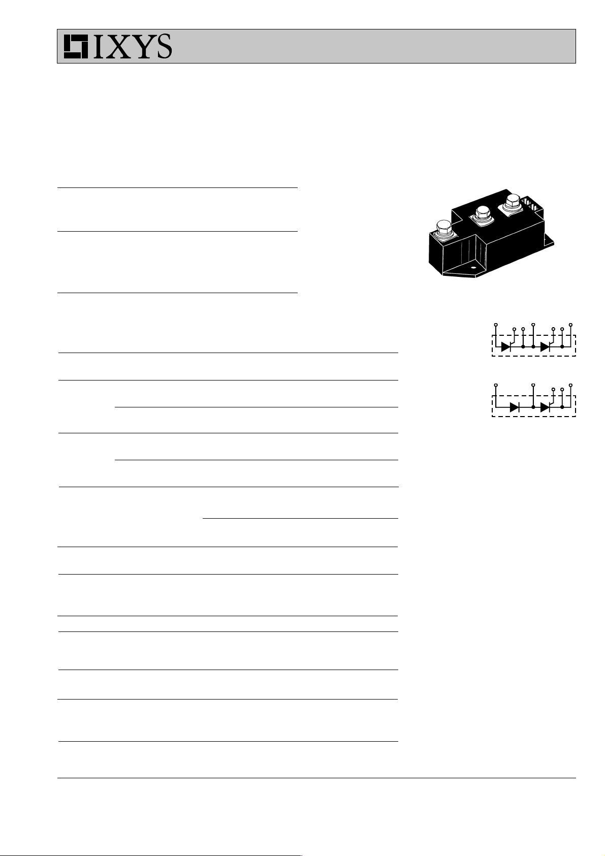
Features
●
International standard package
●
Direct copper bonded Al2O3 -ceramic
base plate
●
Planar passivated chips
●
Isolation voltage 3600 V~
●
UL registered, E 72873
●
Keyed gate/cathode twin pins
Applications
●
Motor control
●
Power converter
●
Heat and temperature control for
industrial furnaces and chemical
processes
●
Lighting control
●
Contactless switches
Advantages
●
Space and weight savings
●
Simple mounting
●
Improved temperature and power
cycling
●
Reduced protection circuits
Data according to IEC 60747 and refer to a single thyristor/diode unless otherwise stated.
IXYS reserves the right to change limits, test conditions and dimensions
© 2000 IXYS All rights reserved
030
1 - 4
Symbol Test Conditions Characteristic Values
I
RRM
I
DRM
, V
V
T
F
V
T0
r
T
V
GT
I
GT
V
GD
I
GD
I
L
I
H
t
gd
t
q
Q
S
I
RM
R
thJC
R
thJK
d
S
d
A
a Maximum allowable acceleration 50 m/s
TVJ= T
IT, IF = 600 A; TVJ = 25°C 1.32 V
For power-loss calculations only (TVJ = 140°C) 0.8 V
VD = 6 V; TVJ = 25°C2V
VD = 6 V; TVJ = 25°C 150 mA
TVJ = T
TVJ = 25°C; tP = 30 ms; VD = 6 V 200 mA
IG = 0.45 A; diG/dt = 0.45 A/ms
TVJ = 25°C; VD = 6 V; RGK = ¥ 150 mA
TVJ = 25°C; VD = 1/2 V
IG = 1 A; diG/dt = 1 A/ms
TVJ = T
VR = 100 V; dv/dt = 50 V/ms; VD = 2/3 V
TVJ = 125°C; IT, IF = 400 A, -di/dt = 50 A/ms 760 mC
per thyristor/diode; DC current 0.112 K/W
per module other values 0.056 K/W
per thyristor/diode; DC current see Fig. 8/9 0.152 K/W
per module 0.076 K/W
Creepage distance on surface 12.7 mm
Strike distance through air 9.6 mm
; VR = V
VJM
RRM
; VD = V
DRM
70 mA
40 mA
0.82 mW
TVJ = -40°C3V
TVJ = -40°C 200 mA
;V
VJM
; IT = 300 A, tP = 200 ms; -di/dt = 10 A/ms typ. 200 ms
VJM
= 2/3 V
D
DRM
DRM
0.25 V
10 mA
DRM
275 A
2 ms
MCC 310
MCD 310
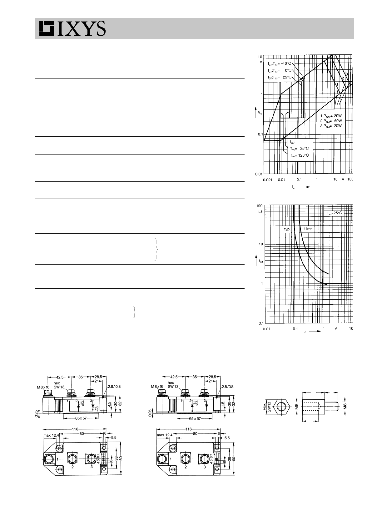
Fig. 1 Gate trigger characteristics
2
Optional accessories for modules
Keyed gate/cathode twin plugs with wire length = 350 mm, gate = yellow, cathode = red
Type ZY 180L (L = Left for pin pair 4/5) UL 758, style 1385,
Type ZY 180R (R = right for pin pair 6/7) CSA class 5851, guide 460-1-1
Dimensions in mm (1 mm = 0.0394")
MCC MCD
Fig. 2 Gate trigger delay time
Threaded spacer for higher Anode/
Cathode construction:
Type ZY 250, material brass
20 12
14
© 2000 IXYS All rights reserved
2 - 4
 Loading...