


IXYS IXDN409SI, IXDN409CI, IXDD409YI, IXDD409PI, IXDD409CI Datasheet
...
|
|
IXDD409PI / 409SI / 409YI / 409CI IXDI409PI / 409SI / 409YI / 409CI |
|||
|
|
IXDN409PI / 409SI / 409YI / 409CI |
|||
|
|
9 Amp Low-Side Ultrafast MOSFET Driver |
|
||
Features |
|
|
General Description |
||
|
|||||
• Built using the advantages and compatibility |
TheIXDD409/IXDI409/IXDN409arehighspeedhighcurrent |
||||
of CMOS and IXYS HDMOSTM processes. |
|||||
gate drivers specifically designed to drive the largest |
|||||
• Latch Up Protected |
|||||
MOSFETs and IGBTs to their minimum switching time and |
|||||
• High Peak Output Current: 9A Peak |
|||||
maximum practical frequency limits. The IXDD409/IXDI409/ |
|||||
• Operates from 4.5V to 25V |
|||||
IXDN409 can source and sink 9A of peak current while |
|||||
• Ability to Disable Output under Faults |
|||||
producing voltage rise and fall times of less than 30ns. The |
|||||
• High Capacitive Load |
|||||
input of the drivers are compatible with TTL or CMOS and are |
|||||
Drive Capability: 2500pF in <15ns |
|||||
fully immune to latch up over the entire operating range. |
|||||
• Matched Rise And Fall Times |
|||||
Designed with small internal delays, cross conduction/ |
|||||
• Low Propagation Delay Time |
|||||
current shoot-through is virtually eliminated in the IXDD409/ |
|||||
• Low Output Impedance |
|||||
IXDI409/IXDN409. Their features and wide safety margin in |
|||||
• Low Supply Current |
|||||
operating voltage and power make the drivers unmatched in |
|||||
|
|
|
|||
Applications |
performanceandvalue. |
||||
The IXDD409 incorporates a unique ability to disable the |
|||||
• Driving MOSFETs and IGBTs |
|||||
output under fault conditions. When a logical low is forced |
|||||
• Motor Controls |
|||||
into the Enable input, both final output stage MOSFETs |
|||||
• LineDrivers |
|||||
(NMOS and PMOS) are turned off. As a result, the output of |
|||||
• Pulse Generators |
|||||
the IXDD409 enters a tristate mode and achieves a Soft Turn- |
|||||
• Local Power ON/OFF Switch |
|||||
Off of the MOSFET/IGBT when a short circuit is detected. |
|||||
• Switch Mode Power Supplies (SMPS) |
|||||
This helps prevent damage that could occur to the MOSFET/ |
|||||
• DC to DC Converters |
|||||
IGBT if it were to be switched off abruptly due to a dv/dt over- |
|||||
• PulseTransformerDriver |
|||||
voltage transient. |
|||||
• Limiting di/dt under Short Circuit |
|||||
|
|
||||
• Class D Switching Amplifiers |
The IXDN409 is configured as a non-inverting gate driver, and |
||||
|
|
|
the IXDI409 is an inverting gate driver. |
||
|
|
|
TheIXDD409/IXDI409/IXDN409areavailableinthestandard8- |
||
|
|
|
pin P-DIP (PI), SOP-8 (SI), 5-pin TO-220 (CI) and in the TO-263 |
||
|
|
|
(YI) surface-mount packages. |
||
|
|
|
|||
Figure 1A - IXDD409 Functional Diagram |
Ordering Information |
||||
Figure 1B - IXDN409 Functional Diagram
Part Number |
Package Type |
Temp. Range |
Configuration |
|||
IXDD409PI |
8-Pin PDIP |
|
|
|
|
|
IXDD409SI |
8-Pin SOIC |
-40° |
C to +85° C |
Non Inverting |
||
IXDD409YI |
5-Pin TO-263 |
With Enable Line |
||||
IXDD409CI |
5-Pin TO-220 |
|
|
|
|
|
IXDI409PI |
8-Pin PDIP |
|
|
|
|
|
IXDI409SI |
8-Pin SOIC |
-40 |
° |
° |
Inverting |
|
IXDI409YI |
5-Pin TO-263 |
|||||
|
C to +85 C |
|
||||
IXDI409CI |
5-Pin TO-220 |
|
|
|
|
|
IXDN409PI |
8-Pin PDIP |
|
|
|
|
|
IXDN409SI |
8-Pin SOIC |
-40 |
° |
° |
Non Inverting |
|
IXDN409YI |
5-Pin TO-263 |
|||||
|
C to +85 C |
|
||||
IXDN409CI |
5-Pin TO-220 |
|
|
|
|
|
Figure 1C - IXDI409 Functional Diagram
Copyright © IXYS CORPORATION 2002 Patent Pending

IXDD409PI / 409SI / 409YI / 409CI |
IXDI409PI / 409SI / 409YI / 409CI |
IXDN409PI / 409SI / 409YI / 409CI |
|
Absolute Maximum Ratings (Note 1)
Parameter |
Value |
|
Supply Voltage |
25 V |
|
All Other Pins |
-0.3 V to VCC + 0.3 V |
|
Power Dissipation, TAMBIENT ≤ 25 oC |
975mW |
|
8 |
Pin PDIP (PI) |
|
8 |
Pin SOIC (SI) |
1055mW |
TO220 (CI), TO263 (YI) |
17W |
|
Derating Factors (to Ambient) |
|
|
8 |
Pin PDIP (PI) |
7.6mW/oC |
8 |
Pin SOIC (SI) |
8.2mW/oC |
TO220 (CI), TO263 (YI) |
0.14W/oC |
|
Storage Temperature |
-65 oC to 150 oC |
|
Lead Temperature (10 sec) |
300 oC |
|
Operating Ratings
Parameter |
Value |
Maximum Junction Temperature |
150 oC |
Operating Temperature Range |
-40 oC to 85 oC |
Thermal Impedance (Junction To Case) |
0.95 oC/W |
TO220 (CI), TO263 (YI) (θ JC) |
Electrical Characteristics
Unless otherwise noted, TA = 25 oC, 4.5V ≤ VCC ≤ |
25V . |
|
|
|
|
|
|
All voltage measurements with respect to GND. IXDD409 configured as described in Test Conditions. |
|
|
|
|
|||
Symbol |
Parameter |
Test Conditions |
Min |
Typ |
Max |
Units |
|
|
|
|
|
|
|
|
|
VIH |
High input voltage |
|
3.5 |
|
|
V |
|
|
|
|
|
|
|
|
|
VIL |
Low input voltage |
|
|
|
0.8 |
V |
|
|
|
|
|
|
|
|
|
VIN |
Input voltage range |
|
-5 |
|
VCC + 0.3 |
V |
|
IIN |
Input current |
0V ≤ VIN ≤ VCC |
-10 |
|
10 |
µ |
A |
|
|
|
|
|
|
|
|
VOH |
High output voltage |
|
VCC - 0.025 |
|
|
V |
|
VOL |
Low output voltage |
|
|
|
0.025 |
V |
|
|
|
|
|
|
|
|
|
ROH |
Output resistance |
IOUT = 10mA, VCC = 18V |
|
0.8 |
1.5 |
Ω |
|
|
@ Output high |
|
|
|
|
|
|
ROL |
Output resistance |
IOUT = 10mA, VCC = 18V |
|
0.8 |
1.5 |
Ω |
|
|
@ Output Low |
|
|
|
|
|
|
IPEAK |
Peak output current |
VCC is 18V |
|
9 |
|
A |
|
|
|
|
|
|
|
|
|
IDC |
Continuous output |
Limited by package power |
|
|
2 |
A |
|
|
current |
dissipation |
|
|
|
|
|
VEN |
Enable voltage range |
IXDD409 Only |
- .3 |
|
Vcc + 0.3 |
V |
|
|
|
|
|
|
|
|
|
VENH |
High En Input Voltage |
IXDD409 Only |
2/3 Vcc |
|
|
V |
|
|
|
|
|
|
|
|
|
VENL |
Low En Input Voltage |
IXDD409 Only |
|
|
1/3 Vcc |
V |
|
|
|
|
|
|
|
|
|
tR |
Rise time |
CL=2500pF Vcc=18V |
8 |
10 |
15 |
ns |
|
tF |
Fall time |
CL=2500pF Vcc=18V |
8 |
10 |
15 |
ns |
|
tONDLY |
On-time propagation |
CL=2500pF Vcc=18V |
33 |
36 |
40 |
ns |
|
|
delay |
|
|
|
|
|
|
tOFFDLY |
Off-time propagation |
CL=2500pF Vcc=18V |
31 |
33 |
36 |
ns |
|
|
delay |
|
|
|
|
|
|
tENOH |
Enable to output high |
IXDD409 Only, Vcc=18V |
|
|
52 |
ns |
|
|
delay time |
|
|
|
|
|
|
tDOLD |
Disable to output low |
IXDD409 Only, Vcc=18V |
|
|
30 |
ns |
|
|
Disable delay time |
|
|
|
|
|
|
VCC |
Power supply voltage |
|
4.5 |
18 |
25 |
V |
|
|
|
|
|
|
|
|
|
ICC |
Power supply current |
VIN = 3.5V |
|
1 |
3 |
mA |
|
|
|
VIN = 0V |
|
0 |
10 |
µ |
A |
|
|
VIN = + VCC |
|
|
10 |
µ |
A |
Specifications Subject To Change Without Notice
2
IXDD409PI / 409SI / 409YI / 409CI |
IXDI409PI / 409SI / 409YI / 409CI |
IXDN409PI / 409SI / 409YI / 409CI |
|
Pin Configurations
1 |
V C C |
VCC |
8 |
|
|
|
|
1 |
|
Vcc |
|
||||
|
|||||||
|
|||||||
2 |
IN |
OUT |
7 |
2 |
|
OUT |
|
|
|||||||
3 |
|
GND |
|
||||
3 |
EN * |
OUT |
6 |
|
|
||
|
|||||||
4 |
|
IN |
|
||||
|
|||||||
4 |
GND |
GND |
5 |
5 |
|
EN* |
|
|
|||||||
|
|||||||
|
|
|
|
|
|
|
|
|
|
|
|
|
|
|
|
|
|
8 PIN DIP (PI) |
TO220(CI) |
|
|
|
SO8 (SI) |
TO263(YI) |
|
Pin Description |
|
|
|
|
|
|
|
|
|
|
SYMBOL |
FUNCTION |
|
DESCRIPTION |
|
VCC |
Supply Voltage |
|
Positive power-supply voltage input. This pin provides power to the |
|
|
entire chip. The range for this voltage is from 4.5V to 25V. |
||
|
|
|
|
|
|
IN |
Input |
|
Input signal-TTL or CMOS compatible. |
|
EN * |
Enable |
|
The system enable pin. This pin, when driven low, disables the chip, |
|
|
forcing high impedance state to the output (IXDD409 Only). |
||
|
|
|
|
|
|
OUT |
Output |
|
Driver Output. For application purposes, this pin is connected, |
|
|
through a resistor, to Gate of a MOSFET/IGBT. |
||
|
|
|
|
|
|
|
|
|
The system ground pin. Internally connected to all circuitry, this pin |
|
GND |
Ground |
|
provides ground reference for the entire chip. This pin should be |
|
|
connected to a low noise analog ground plane for optimum |
||
|
|
|
|
|
|
|
|
|
performance. |
* This pin is used only on the IXDD409, and is N/C on the IXDI409 and IXDN409.
Note 1: Operating the device beyond parameters with listed “absolute maximum ratings” may cause permanent damage to the device. Typical values indicate conditions for which the device is intended to be functional, but do not guarantee specific performance limits. The guaranteed specifications apply only for the test conditions listed. Exposure to absolute maximum rated conditions for extended periods may affect device reliability.
CAUTION: These devices are sensitive to electrostatic discharge; follow proper ESD procedures when handling and assembling this component.
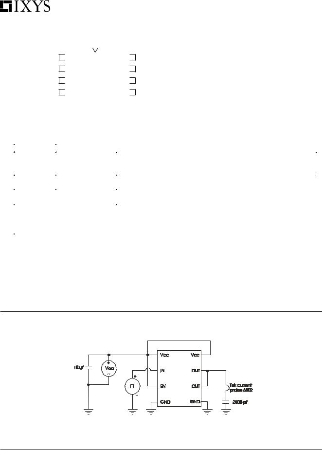
Figure 2 - Characteristics Test Diagram
VIN
3
 Loading...