


ISSI IS89C52-40PQI, IS89C52-40PQ, IS89C52-24WI, IS89C52-24W, IS89C52-24PQI Datasheet
...
|
|
|
|
ISSI |
|
|
|
|
|
|
IS89C52 |
|
|
|
|
® |
|
|
|
|
IS89C52 |
|
|
|
|
|
|
|
|
|
|
|
|
|
|
|
|
|
|
|
CMOS SINGLE CHIP |
NOVEMBER 1998 |
|
|
|
||||
8-BIT MICROCONTROLLER with 8-Kbytes of FLASH
FEATURES
•80C51 based architecture
•8-Kbytes of on-chip Reprogrammable Flash Memory
•256 x 8 RAM
•Three 16-bit Timer/Counters
•Full duplex serial channel
•Boolean processor
•Four 8-bit I/O ports, 32 I/O lines
•Memory addressing capability
–64K ROM and 64K RAM
•Program memory lock
–Lock bits (3)
•Power save modes:
–Idle and power-down
•Eight interrupt sources
•Most instructions execute in 0.3 μs
•CMOS and TTL compatible
•Maximum speed: 40 MHz @ Vcc = 5V
•Industrial temperature available
•Packages available:
–40-pin DIP
–44-pin PLCC
–44-pin PQFP
GENERAL DESCRIPTION
The ISSI IS89C52 is a high-performance microcontroller fabricated using high-density CMOS technology. The CMOS IS89C52 is functionally compatible with the industry standard 80C51 microcontrollers.
The IS89C52 is designed with 8-Kbytes of Flash memory, 258 x 8 RAM; 32 programmable I/O lines; a serial I/O port for either multiprocessor communications, I/O expansion or full duplex UART; three 16-bit timer/counters; an eight-source, two-priority-level, nested interrupt structure; and an on-chip oscillator and clock circuit. The IS89C52 can be expanded using standard TTL compatible memory.
|
|
|
|
T2/P1.0 |
|
1 |
40 |
|
VCC |
|||||||
T2EX/P1.1 |
|
39 |
|
P0.0/AD0 |
||||||||||||
|
2 |
|
||||||||||||||
|
|
|
|
|
|
P1.2 |
|
38 |
|
P0.1/AD1 |
||||||
|
|
|
|
|
|
|
3 |
|
||||||||
|
|
|
|
|
|
P1.3 |
|
37 |
|
P0.2/AD2 |
||||||
|
|
|
|
|
|
|
4 |
|
||||||||
|
|
|
|
|
|
P1.4 |
|
36 |
|
P0.3/AD3 |
||||||
|
|
|
|
|
|
|
5 |
|
||||||||
|
|
|
|
|
|
P1.5 |
|
35 |
|
P0.4/AD4 |
||||||
|
|
|
|
|
|
|
6 |
|
||||||||
|
|
|
|
|
|
P1.6 |
|
34 |
|
P0.5/AD5 |
||||||
|
|
|
|
|
|
|
7 |
|
||||||||
|
|
|
|
|
|
P1.7 |
|
8 |
33 |
|
P0.6/AD6 |
|||||
|
|
|
|
|
|
|
|
|||||||||
|
|
|
|
|
|
RST |
|
32 |
|
P0.7/AD7 |
||||||
|
|
|
|
|
|
|
9 |
|
||||||||
|
|
RxD/P3.0 |
|
|
31 |
|
|
|
|
|
|
|
||||
|
|
|
10 |
|
|
EA/VPP |
||||||||||
|
|
TxD/P3.1 |
|
|
30 |
|
|
|
|
|
|
|
||||
|
|
|
11 |
|
ALE/PROG |
|
||||||||||
|
|
|
|
|
|
|
|
|
29 |
|
|
|
|
|
|
|
|
INT0/P3.2 |
|
12 |
|
|
PSEN |
|
|
||||||||
|
|
|
|
|
|
|
|
|
28 |
|
P2.7/A15 |
|||||
|
INT1/P3.3 |
|
13 |
|
||||||||||||
|
|
|
|
T0/P3.4 |
|
14 |
27 |
|
P2.6/A14 |
|||||||
|
|
|||||||||||||||
|
|
|
|
T1/P3.5 |
|
15 |
26 |
|
P2.5/A13 |
|||||||
|
|
|||||||||||||||
|
|
|
|
|
|
|
16 |
25 |
|
P2.4/A12 |
||||||
WR/P3.6 |
|
|
||||||||||||||
|
|
|
|
|
|
|
|
17 |
24 |
|
P2.3/A11 |
|||||
RD/P3.7 |
|
|
||||||||||||||
|
|
|
|
XTAL2 |
|
18 |
23 |
|
P2.2/A10 |
|||||||
|
|
|||||||||||||||
|
|
|
|
XTAL1 |
|
19 |
22 |
|
P2.1/A9 |
|||||||
|
|
|||||||||||||||
|
|
|
|
|
|
GND |
|
20 |
21 |
|
P2.0/A8 |
|||||
|
|
|||||||||||||||
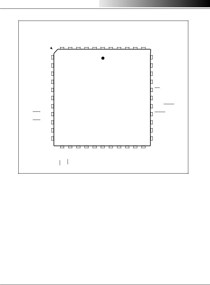
Figure 1. IS89C52 Pin Configuration: 40-pin PDIP
ISSI reserves the right to make changes to its products at any time without notice in order to improve design and supply the best possible product. We assume no responsibility for any errors which may appear in this publication. © Copyright 1998, Integrated Silicon Solution, Inc.
Integrated Silicon Solution, Inc. — 1-800-379-4774 |
1 |
MC013-1C 11/21/98
IS89C52 |
|
|
|
|
|
|
|
|
|
|
|
|
INDEX |
P1.4 |
P1.3 |
P1.2 |
P1.1/T2EX |
P1.0/T2 |
NC |
VCC |
P0.0/AD0 |
P0.1/AD1 |
P0.2/AD2 |
P0.3/AD3 |
|
|
|
|
|
|
|
|
|
|
|
|
|
|
|
6 |
5 |
4 |
3 |
2 |
1 |
44 |
43 |
42 |
41 |
40 |
|
P1.5 |
7 |
|
|
|
|
|
|
|
|
|
39 |
P0.4/AD4 |
P1.6 |
8 |
|
|
|
|
|
|
|
|
|
38 |
P0.5/AD5 |
P1.7 |
9 |
|
|
|
|
|
|
|
|
|
37 |
P0.6/AD6 |
RST |
10 |
|
|
|
|
|
|
|
|
|
36 |
P0.7/AD7 |
RxD/P3.0 |
11 |
|
|
|
|
|
|
|
|
|
35 |
EA/VPP |
NC |
12 |
|
|
|
TOP VIEW |
|
|
|
34 |
NC |
||
|
|
|
|
|
|
|
|
|
||||
TxD/P3.1 |
13 |
|
|
|
|
|
|
|
|
|
33 |
ALE/PROG |
INT0/P3.2 |
14 |
|
|
|
|
|
|
|
|
|
32 |
PSEN |
INT1/P3.3 |
15 |
|
|
|
|
|
|
|
|
|
31 |
P2.7/A15 |
T0/P3.4 |
16 |
|
|
|
|
|
|
|
|
|
30 |
P2.6/A14 |
T1/P3.5 |
17 |
|
|
|
|
|
|
|
|
|
29 |
P2.5/A13 |
|
18 |
19 |
20 |
21 |
22 |
23 |
24 |
25 |
26 |
27 |
28 |
|
|
WR/P3.6 |
RD/P3.7 |
XTAL2 |
XTAL1 |
GND |
NC |
A8/P2.0 |
A9/P2.1 |
A10/P2.2 |
A11/P2.3 |
A12/P2.4 |
|
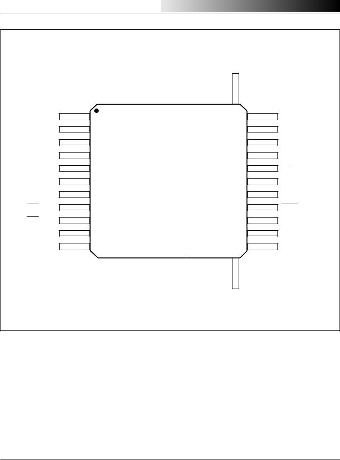
Figure 2. IS89C52 Pin Configuration: 44-pin PLCC
2 |
Integrated Silicon Solution, Inc. — 1-800-379-4774 |
MC013-1C 11/21/98
IS89C52
P1.5
P1.6
P1.7
RST
RxD/P3.0
NC
TxD/P3.1
INT0/P3.2
INT1/P3.3
T0/P3.4
T1/P3.5
1
2
3
4
5
6
7
8
9
10
11
P1.4 |
|
P1.3 |
P1.2 |
P1.1/T2EX |
P1.0/T2 |
NC |
|
VCC |
P0.0/AD0 |
P0.1/AD1 |
P0.2/AD2 |
|||||||||
|
|
|
|
|
|
|
|
|
|
|
|
|
|
|
|
|
|
|
|
|
|
|
|
|
|
|
|
|
|
|
|
|
|
|
|
|
|
|
|
|
|
44 |
43 |
42 |
41 |
40 |
39 |
38 |
37 |
36 |
35 |
|||||||||||
|
12 |
13 |
14 |
15 |
16 |
17 |
18 |
19 |
20 |
21 |
|||||||||
|
|
|
|
|
|
|
|
|
|
|
|
|
|
|
|
|
|
|
|
|
WR/P3.6 |
|
RD/P3.7 |
|
XTAL2 |
XTAL1 |
GND |
NC |
A8/P2.0 |
|
A9/P2.1 |
|
A10/P2.2 |
|
A11/P2.3 |
||||
|
|
|
|
|
|
|
|
|
|
||||||||||
|
|
|
|
|
|
|
|
|
|
|
|
|
|
|
|
|
|||
P0.3/AD3
34
33
32
31
30
29
29
27
26
25
24
23
22 A12/P2.4
P0.4/AD4
P0.5/AD5
P0.6/AD6
P0.7/AD7
EA
NC
ALE
PSEN
P2.7/A15
P2.6/A14
P2.5/A13
Figure 3. IS89C52 Pin Configuration: 44-pin PQFP
Integrated Silicon Solution, Inc. — 1-800-379-4774 |
3 |
MC013-1C 11/21/98

IS89C52 |
|
|
|
|
|
|
|
|
|
|
|
|
|
|
|
P2.0-P2.7 |
P0.0-P0.7 |
|
|
|
|
|
|
|
|
P2 |
P0 |
|
|
Vcc |
|
|
|
|
|
DRIVERS |
DRIVERS |
|
|
|
|
|
|
|
|
|
|
|
|
GND |
|
|
|
|
|
|
|
|
|
|
|
|
ADDRESS |
|
|
|
ADDRESS |
3 LOCK BITS |
|
|
|
|
DECODER |
|
|
|
DECODER |
& |
|
|
RAM ADDR |
& 256 |
|
P2 |
P0 |
& |
32 BYTES |
||
|
REGISTER |
BYTES RAM |
|
LATCH |
LATCH |
8K FLASH |
ENCRYPTION |
||
|
|
|
|
|
|
|
|
|
PROGRAM |
|
|
|
|
|
|
|
|
|
ADDRESS |
|
B |
|
STACK |
|
ACC |
|
|
REGISTER |
|
|
REGISTER |
POINT |
|
|
|
|
|||
|
|
|
|
|
|
||||
|
|
|
PCON |
SCON |
TMOD |
TCON |
|
|
PROGRAM |
|
|
|
T2CON |
TH0 |
TL0 |
TH1 |
TMP2 |
TMP1 |
COUNTER |
|
|
|
|
||||||
|
|
|
TL1 |
TH2 |
TL2 |
RCAP2H |
|
|
|
|
|
|
RCAP2L |
SBUF |
IE |
IP |
|
|
|
|
|
|
INTERRUPT BLOCK |
|
|
PC |
|||
|
|
|
SERIAL PORT BLOCK |
ALU |
|
INCREMENTER |
|||
|
|
|
|
TIMER BLOCK |
|
|
|
|
|
|
|
|
|
|
|
|
PSW |
|
BUFFER |
|
|
|
|
|
|
|
|
|
|
PSEN |
|
INSTRUCTION REGISTER |
|
|
|
|
|
|
|
ALE/PROG |
TIMING |
|
|
|
|
|
DPTR |
||
RST |
AND |
|
|
|
|
|
|||
CONTROL |
|
|
|
|
|
|
|||
EA/VPP |
|
|
|
|
|
|
|
||
|
|
|
|
|
|
|
|
||
|
|
|
|
|
|
P3 |
|
P1 |
|
|
|
|
|
|
|
LATCH |
|
LATCH |
|
|
OSCILLATOR |
|
|
|
|
|
|
|
|
|
XTAL1 |
|
XTAL2 |
|
|
P3 |
|
P1 |
|
|
|
|
|
DRIVERS |
|
DRIVERS |
|
||
|
|
|
|
|
|
|
|
||
|
|
|
|
|
|
P3.0-P3.7 |
|
P1.0-P1.7 |
|
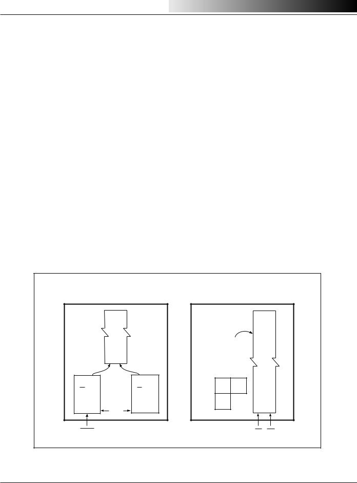
Figure 4. IS89C52 Block Diagram
4 |
Integrated Silicon Solution, Inc. — 1-800-379-4774 |
MC013-1C 11/21/98

IS89C52
Table 1. Detailed Pin Description
Symbol |
PDIP |
PLCC |
PQFP |
I/O |
Name and Function |
ALE/PROG |
30 |
33 |
27 |
I/O |
Address Latch Enable: Output pulse for latching the low byte |
|
|
|
|
|
of the address during an address to the external memory. In |
|
|
|
|
|
normal operation, ALE is emitted at a constant rate of 1/6 the |
|
|
|
|
|
oscillator frequency, and can be used for external timing or |
|
|
|
|
|
clocking. Note that one ALE pulse is skipped during each |
|
|
|
|
|
access to external data memory. This pin is also the Program |
|
|
|
|
|
Pulse input (PROG) during Flash programming. |
|
|
|
|
|
|
EA/VPP |
31 |
35 |
29 |
I |
External Access enable: EA must be externally held low to |
|
|
|
|
|
enable the device to fetch code from external program memory |
|
|
|
|
|
locations 0000H to FFFFH. If EA is held high, the device |
|
|
|
|
|
executes from internal program memory unless the program |
|
|
|
|
|
counter contains an address greater than 0FFFH. This also |
|
|
|
|
|
receives the 12V programming enable voltage (VPP) during |
|
|
|
|
|
Flash programming. |
|
|
|
|
|
|
P0.0-P0.7 |
39-32 |
43-36 |
37-30 |
I/O |
Port 0: Port 0 is an 8-bit open-drain, bidirectional I/O port. Port |
|
|
|
|
|
0 pins that have 1s written to them float and can be used as high- |
|
|
|
|
|
impedance inputs. Port 0 is also the multiplexed low-order |
|
|
|
|
|
address and data bus during accesses to external program and |
|
|
|
|
|
data memory. In this application, it uses strong internal pullups |
|
|
|
|
|
when emitting 1s. |
|
|
|
|
|
Port 0 also receives the code bytes during programmable |
|
|
|
|
|
memory programming and outputs the code bytes during |
|
|
|
|
|
program verification. External pullups are required during pro- |
|
|
|
|
|
gram verification. |
|
|
|
|
|
|
P1.0-P1.7 |
1-8 |
2-9 |
40-44 |
I/O |
Port 1: Port 1 is an 8-bit bidirectional I/O port with internal |
|
|
|
1-3 |
|
pullups. Port 1 pins that have 1s written to them are pulled high |
|
|
|
|
|
by the internal pullups and can be used as inputs. As inputs, |
|
|
|
|
|
Port 1 pins that are externally pulled low will source current |
|
|
|
|
|
because of the internal pullups. (See DC Characteristics: IIL). |
|
|
|
|
|
The Port 1 output buffers can sink/source four TTL inputs. |
|
|
|
|
|
Port 1 also receives the low-order address byte during Flash |
|
|
|
|
|
programming and verification. |
|
1 |
2 |
40 |
I |
T2(P1.0): Timer/Counter 2 external count input. |
|
2 |
3 |
41 |
I |
T2EX(P1.1): Timer/Counter 2 trigger input. |
|
|
|
|
|
|
P2.0-P2.7 |
21-28 |
24-31 |
18-25 |
I/O |
Port 2: Port 2 is an 8-bit bidirectional I/O port with internal |
|
|
|
|
|
pullups. Port 2 pins that have 1s written to them are pulled high |
|
|
|
|
|
by the internal pullups and can be used as inputs. As inputs, |
|
|
|
|
|
Port 2 pins that are externally pulled low will source current |
|
|
|
|
|
because of the internal pullups. (See DC Characteristics: IIL). |
|
|
|
|
|
Port 2 emits the high order address byte during fetches from |
|
|
|
|
|
external program memory and during accesses to external data |
|
|
|
|
|
memory that used 16-bit addresses (MOVX @ DPTR). In this |
|
|
|
|
|
application, Port 2 uses strong internal pullups when emitting |
|
|
|
|
|
1s. During accesses to external data memory that use 8-bit |
|
|
|
|
|
addresses (MOVX @ Ri [i = 0, 1]), Port 2 emits the contents of |
|
|
|
|
|
the P2 Special Function Register. |
|
|
|
|
|
Port 2 also receives the high-order bits and some control |
|
|
|
|
|
signals during Flash programming and verification. P2.6 and |
|
|
|
|
|
P2.7 are the control signals while the chip programs and |
|
|
|
|
|
erases. |
|
|
||||
|
|
|
|
|
|
Integrated Silicon Solution, Inc. — 1-800-379-4774 |
5 |
||||
MC013-1C |
|
|
|
|
|
11/21/98 |
|
|
|
|
|

IS89C52
Table 1. Detailed Pin Description (continued)
Symbol |
PDIP |
PLCC |
PQFP |
I/O |
Name and Function |
P3.0-P3.7 |
10-17 |
11, 13-19 |
5, 7-13 |
I/O |
Port 3: Port 3 is an 8-bit bidirectional I/O port with internal |
|
|
|
|
|
pullups. Port 3 pins that have 1s written to them are pulled high |
|
|
|
|
|
by the internal pullups and can be used as inputs. As inputs, |
|
|
|
|
|
Port 3 pins that are externally pulled low will source current |
|
|
|
|
|
because of the internal pullups. (See DC Characteristics: IIL). |
|
|
|
|
|
Port 3 also serves the special features of the IS89C52, as listed |
|
|
|
|
|
below: |
|
10 |
11 |
5 |
I |
RxD (P3.0): Serial input port. |
|
11 |
13 |
7 |
O |
TxD (P3.1): Serial output port. |
|
12 |
14 |
8 |
I |
INT0 (P3.2): External interrupt 0. |
|
13 |
15 |
9 |
I |
INT1 (P3.3): External interrupt 1. |
|
14 |
16 |
10 |
I |
T0 (P3.4): Timer 0 external input. |
|
15 |
17 |
11 |
I |
T1 (P3.5): Timer 1 external input. |
|
16 |
18 |
12 |
O |
WR (P3.6): External data memory write strobe. |
|
17 |
19 |
13 |
O |
RD (P3.7): External data memory read strobe. |
|
|
|
|
|
|
PSEN |
29 |
32 |
26 |
O |
Program Store Enable: The read strobe to external program |
|
|
|
|
|
memory. When the device is executing code from the external |
|
|
|
|
|
program memory, PSEN is activated twice each machine cycle |
|
|
|
|
|
except that two PSEN activations are skipped during each |
|
|
|
|
|
access to external data memory. PSEN is not activated during |
|
|
|
|
|
fetches from internal program memory. |
|
|
|
|
|
|
RST |
9 |
10 |
4 |
I |
Reset: A high on this pin for two machine cycles while the |
|
|
|
|
|
oscillator is running, resets the device. An internal MOS resistor |
|
|
|
|
|
to GND permits a power-on reset using only an external |
|
|
|
|
|
capacitor connected to Vcc. |
|
|
|
|
|
|
XTAL 1 |
19 |
21 |
15 |
I |
Crystal 1: Input to the inverting oscillator amplifier and input |
|
|
|
|
|
to the internal clock generator circuits. |
|
|
|
|
|
|
XTAL 2 |
18 |
20 |
14 |
O |
Crystal 2: Output from the inverting oscillator amplifier. |
|
|
|
|
|
|
GND |
20 |
22 |
16 |
I |
Ground: 0V reference. |
|
|
|
|
|
|
Vcc |
40 |
44 |
38 |
I |
Power Supply: This is the power supply voltage for operation. |
|
|
|
|
|
|
6 Integrated Silicon Solution, Inc. — 1-800-379-4774
MC013-1C 11/21/98
IS89C52
OPERATING DESCRIPTION
The detail description of the IS89C52 included in this description are:
•Memory Map and Registers
•Timer/Counters
•Serial Interface
•Interrupt System
•Other Information
•Flash Memory
MEMORY MAP AND REGISTERS
Memory
The IS89C52 has separate address spaces for program and data memory. The program and data memory can be up to 64K bytes long. The lower 8K program memory can reside on-chip. Figure 5 shows a map of the IS89C52 program and data memory.
The IS89C52 has 256 bytes of on-chip RAM, plus numbers of special function registers. The lower 128 bytes can be accessed either by direct addressing or by indirect
addressing. Figure 6 shows internal data memory organization and SFR Memory Map.
The lower 128 bytes of RAM can be divided into three segments as listed below and shown in Figure 7.
1.Register Banks 0-3: locations 00H through 1FH (32 bytes). The device after reset defaults to register bank 0. To use the other register banks, the user must select them in software. Each register bank contains eight 1-byte registers R0-R7. Reset initializes the stack point to location 07H, and is incremented once to start from 08H, which is the first register of the second register bank.
2.Bit Addressable Area: 16 bytes have been assigned for this segment 20H-2FH. Each one of the 128 bits of this segment can be directly addressed (0-7FH). Each of the 16 bytes in this segment can also be addressed as a byte.
3.Scratch Pad Area: 30H-7FH are available to the user as data RAM. However, if the data pointer has been initialized to this area, enough bytes should be left aside to prevent SP data destruction.
Program Memory |
Data Memory |
(Read Only) |
(Read/Write) |
FFFFH: |
|
|
FFFFH: |
64K |
|
|
|
|
|
|
External |
|
1FFFH: |
|
Internal |
|
FFH: |
|
|
|
8K |
|
|
|
|
|
|
EA = 0 |
|
EA = 1 |
|
External |
|
Internal |
|
|
0000 |
00 |
0000 |
|
|
|
|
PSEN |
|
|
RD WR |
Figure 5. IS89C52 Program and Data Memory Structure
Integrated Silicon Solution, Inc. — 1-800-379-4774 |
7 |
MC013-1C 11/21/98

IS89C52
SPECIAL FUNCTION REGISTERS
The Special Function Registers (SFR's) are located in upper 128 Bytes direct addressing area. The SFR Memory Map in Figure 6 shows that.
Not all of the addresses are occupied. Unoccupied addresses are not implemented on the chip. Read accesses to these addresses in general return random data, and write accesses have no effect.
User software should not write 1s to these unimplemented locations, since they may be used in future microcontrollers to invoke new features. In that case, the reset or inactive values of the new bits will always be 0, and their active values will be 1.
The functions of the SFRs are outlined in the following sections, and detailed in Table 2.
Accumulator (ACC)
ACC is the Accumulator register. The mnemonics for Accumulator-specific instructions, however, refer to the Accumulator simply as A.
B Register (B)
The B register is used during multiply and divide operations. For other instructions it can be treated as another scratch pad register.
Program Status Word (PSW). The PSW register contains program status information.
|
FFH |
|
|
FFH |
F8 |
|
|
|
|
|
|
|
|
|
|
|
FF |
|
|
|
|
|
|
|
|
|
|
|
|
|
|
||||
|
|
|
|
|
F0 |
|
B |
|
|
|
|
|
|
|
|
F7 |
|
|
|
|
|
|
E8 |
|
|
|
|
|
|
|
|
|
|
|
EF |
|
|
Accessible |
Accessible |
|
E0 |
|
ACC |
|
|
|
|
|
|
|
|
E7 |
|
Upper |
|
by Indirect |
|
D8 |
|
|
|
|
|
|
|
|
|
|
|
DF |
|
|
by Direct |
|
|
|
|
|
|
|
|
|
|
|
|
||||
128 |
|
Addressing |
|
D0 |
|
PSW |
|
|
|
|
|
|
|
|
D7 |
||
|
Addressing |
|
|
|
|
|
|
|
|
|
|
||||||
|
|
Only |
|
C8 |
|
T2CON |
|
|
RCAP2L |
RCAP2H |
TL2 |
TH2 |
|
|
CF |
||
|
|
|
|
C0 |
|
|
|
|
|
|
|
|
|
|
|
C7 |
|
|
|
|
|
|
|
|
|
|
|
|
|
|
|
|
|
||
|
|
|
|
|
B8 |
|
IP |
|
|
|
|
|
|
|
|
BF |
|
|
80H |
|
|
80H |
B0 |
|
P3 |
|
|
|
|
|
|
|
|
B7 |
|
|
|
|
A8 |
|
IE |
|
|
|
|
|
|
|
|
AF |
|||
|
7FH |
|
|
|
A0 |
|
P2 |
|
|
|
|
|
|
|
|
A7 |
|
|
|
|
|
|
98 |
|
SCON |
|
SBUF |
|
|
|
|
|
|
9F |
|
|
|
Accessible |
|
|
90 |
|
P1 |
|
|
|
|
|
|
|
|
97 |
|
Lower |
|
|
Ports, |
88 |
|
TCON |
|
TMOD |
TL0 |
TL1 |
TH0 |
TH1 |
|
|
8F |
||
|
by Direct |
|
|
|
|
|
|||||||||||
|
|
Status and |
80 |
|
P0 |
|
SP |
DPL |
DPH |
|
|
|
PCON |
87 |
|||
128 |
|
and Indirect |
|
|
|
|
|
|
|||||||||
|
Special |
Control Bits, |
|
|
|
|
|
|
|
|
|
|
|
|
|
||
|
|
Addressing |
Timer, |
|
|
|
|
|
|
|
|
|
|
|
|
|
|
|
|
|
Function |
|
|
|
|
|
|
|
|
|
|
|
|
|
|
|
|
|
Registers, |
|
|
Bit |
|
|
|
|
|
|
|
|
|||
|
|
|
Registers |
|
|
|
|
|
|
|
|
|
|
||||
|
|
|
Stack Pointer, |
|
|
|
|
|
|
|
|
|
|
||||
|
|
|
|
|
Addressable |
|
|
|
|
|
|
|
|
||||
|
0 |
|
|
Accumulator |
|
|
|
|
|
|
|
|
|
|
|
|
|
|
|
|
(Etc.) |
|
|
|
|
|
|
|
|
|
|
|
|
|
|
|
|
|
|
|
|
|
|
|
|
|
|
|
|
|
|
||
Figure 6. Internal Data Memory and SFR Memory Map
|
|
8 BYTES |
|
|
|
|
|
|
|
|
|
|
|
|
|
|
|
|
|
|
|
|
|
|
||
|
|
|
|
|
|
|
|
|
|
|
|
|
|
|
|
|
|
78 |
|
|
|
|
7F |
|
|
|
70 |
|
|
|
|
77 |
|
|
|
68 |
|
|
|
|
6F |
|
|
|
60 |
|
|
|
|
67 |
|
|
|
58 |
|
|
|
|
5F |
SCRATCH |
|
|
50 |
|
|
|
|
57 |
|
||
|
|
|
|
PAD |
|
|||
48 |
|
|
|
|
4F |
AREA |
|
|
|
|
|
|
|
|
|||
40 |
|
|
|
|
47 |
|
|
|
38 |
|
|
|
|
3F |
|
|
|
30 |
|
|
|
|
37 |
|
|
|
|
|
|
|
|
|
|
|
|
28 |
|
|
...7F |
2F |
BIT |
|
||
|
|
|
|
ADDRESSABLE |
|
|||
20 |
0 ... |
|
|
|
27 |
|
||
|
|
|
SEGMENT |
|
||||
|
|
BANK3 |
|
|
|
|
||
18 |
|
1F |
|
|
||||
|
|
|
|
|
|
|||
10 |
|
BANK2 |
17 |
REGISTER |
|
|||
|
|
|
|
|
||||
08 |
|
BANK 1 |
0F |
BANKS |
|
|||
00 |
|
BANK 0 |
07 |
|
|
|||
|
|
|
|
|
|
|||
|
|
|
|
|
|
|
|
|
|
Figure 7. Lower 128 Bytes of Internal RAM |
8 |
Integrated Silicon Solution, Inc. — 1-800-379-4774 |
MC013-1C 11/21/98

IS89C52
SPECIAL FUNCTION REGISTERS
(Continued)
Stack Pointer (SP)
The Stack Pointer Register is eight bits wide. It is incremented before data is stored during PUSH and CALL executions. While the stack may reside anywhere in onchip RAM, the Stack Pointer is initialized to 07H after a reset. This causes the stack to begin at location 08H.
Data Pointer (DPTR)
The Data Pointer consists of a high byte (DPH) and a low byte (DPL). Its function is to hold a 16-bit address. It may be manipulated as a 16-bit register or as two independent 8-bit registers.
Ports 0 To 3
P0, P1, P2, and P3 are the SFR latches of Ports 0, 1, 2, and 3, respectively.
Serial Data Buffer (SBUF)
The Serial Data Buffer is actually two separate registers, a transmit buffer and a receive buffer register. When data is moved to SBUF, it goes to the transmit buffer, where it is held for serial transmission. (Moving a byte to SBUF initiates the transmission.) When data is moved from SBUF, it comes from the receive buffer.
Timer Registers
Register pairs (TH0, TL0) and (TH1, TL1) are the 16-bit Counter registers for Timer/Counters 0 and 1, respectively.
Capture Registers
The register pair (RCAP2H, RCAP2L) are the Capture registers for the Timer 2 Capture Mode. In this mode, in response to a transition at the IS89C52's T2EX pin, TH2 and TL2 are copied into RCAP2H and RCAP2L. Timer 2 also has a 16-bit auto-reload mode, and RCAP2H and RCAP2L hold the reload value for this mode.
Control Registers
Special Function Registers IP, IE, TMOD, TCON, SCON, and PCON contain control and status bits for the interrupt system, the Timer/Counters, and the serial port. They are described in later sections of this chapter.
Integrated Silicon Solution, Inc. — 1-800-379-4774 |
9 |
MC013-1C 11/21/98

IS89C52
Table 2. Special Function Registers
Symbol |
|
Description |
Direct Address |
Bit Address, Symbol, or Alternative Port Function |
Reset Value |
||||||||
ACC(1) |
|
Accumulator |
|
E0H |
E7 |
E6 |
E5 |
E4 |
E3 |
E2 |
E1 |
E0 |
00H |
B(1) |
|
B register |
|
F0H |
F7 |
F6 |
F5 |
F4 |
F3 |
F2 |
F1 |
F0 |
00H |
DPH |
Data pointer (DPTR) high |
83H |
|
|
|
|
|
|
|
|
00H |
||
DPL |
Data pointer (DPTR) low |
|
82H |
|
|
|
|
|
|
|
|
00H |
|
|
|
|
|
|
AF |
AE |
AD |
AC |
AB |
AA |
A9 |
A8 |
|
IE(1) |
|
Interrupt enable |
|
A8H |
EA |
— |
— |
ES |
ET1 |
EX1 |
ET0 |
EX0 |
0XX00000B |
|
|
|
|
|
BF |
BE |
BD |
BC |
BB |
BA |
B9 |
B8 |
|
IP(1) |
|
Interrupt priority |
|
B8H |
— |
— |
— |
PS |
PT1 |
PX1 |
PT0 |
PX0 |
XXX00000B |
|
|
|
|
|
87 |
86 |
85 |
84 |
83 |
82 |
81 |
80 |
|
P0(1) |
|
Port 0 |
|
80H |
P0.7 |
P0.6 |
P0.5 |
P0.4 |
P0.3 |
P0.2 |
P0.1 |
P0.0 |
FFH |
|
|
|
|
|
AD7 |
AD6 |
AD5 |
AD4 |
AD3 |
AD2 |
AD1 |
AD0 |
|
|
|
|
|
|
97 |
96 |
95 |
94 |
93 |
92 |
91 |
90 |
|
P1(1) |
|
Port 1 |
|
90H |
P1.7 |
P1.6 |
P1.5 |
P1.4 |
P1.3 |
P1.2 |
P1.1 |
P1.0 |
FFH |
|
|
|
|
|
A7 |
A6 |
A5 |
A4 |
A3 |
A2 |
A1 |
A0 |
|
P2(1) |
|
Port 2 |
|
A0H |
P2.7 |
P2.6 |
P2.5 |
P2.4 |
P2.3 |
P2.2 |
P2.1 |
P2.0 |
FFH |
|
|
|
|
|
AD15 |
AD14 |
AD13 |
AD12 |
AD11 |
AD10 |
AD9 |
AD8 |
|
|
|
|
|
|
B7 |
B6 |
B5 |
B4 |
B3 |
B2 |
B1 |
B0 |
|
P3(1) |
|
Port 3 |
|
B0H |
P3.7 |
P3.6 |
P3.5 |
P3.4 |
P3.3 |
P3.2 |
P3.1 |
P3.0 |
FFH |
|
|
|
|
|
RD |
WR |
T1 |
T0 |
INT1 |
INT0 |
TXD |
RXD |
|
PCON |
|
Power control |
|
87H |
SMOD |
— |
— |
— |
GF1 |
GF0 |
PD |
IDL |
0XXX0000B |
|
|
|
|
|
D7 |
D6 |
D5 |
D4 |
D3 |
D2 |
D1 |
D0 |
|
PSW(1) |
|
Program status word |
|
D0H |
CY |
AC |
F0 |
RS1 |
RS0 |
OV |
— |
P |
00H |
SBUF |
|
Serial data buffer |
|
99H |
|
|
|
|
|
|
|
|
XXXXXXXXB |
|
|
|
|
|
9F |
9E |
9D |
9C |
9B |
9A |
99 |
98 |
|
SCON(1) |
|
Serial controller |
|
98H |
SM0 |
SM1 |
SM2 |
REN |
TB8 |
RB8 |
TI |
RI |
00H |
SP |
|
Stack pointer |
|
81H |
|
|
|
|
|
|
|
|
07H |
|
|
|
|
|
8F |
8E |
8D |
8C |
8B |
8A |
89 |
88 |
|
TCON(1) |
|
Timer control |
|
88H |
TF1 |
TR1 |
TF0 |
TR0 |
IE1 |
IT1 |
IE0 |
IT0 |
00H |
TMOD |
|
Timer mode |
|
89H |
GATE |
C/T |
M1 |
M0 |
GATE |
C/T |
M1 |
M0 |
00H |
TH0 |
|
Timer high 0 |
|
8CH |
|
|
|
|
|
|
|
|
00H |
TH1 |
|
Timer high 1 |
|
8DH |
|
|
|
|
|
|
|
|
00H |
TL0 |
|
Timer low 0 |
|
8AH |
|
|
|
|
|
|
|
|
00H |
TL1 |
|
Timer low 1 |
|
8BH |
|
|
|
|
|
|
|
|
00H |
RCAP2H(2) |
Capture high |
|
CAH |
|
|
|
|
|
|
|
|
00H |
|
RCAP2L(2) |
Capture low |
|
CBH |
|
|
|
|
|
|
|
|
00H |
|
TL2(2) |
|
Timer low 2 |
|
CCH |
|
|
|
|
|
|
|
|
00H |
Notes:
1.Denotes bit addressable.
2.SFRs are added to the 80C51 SFRs.
10 Integrated Silicon Solution, Inc. — 1-800-379-4774
MC013-1C 11/21/98
IS89C52
The detail description of each bit is as follows:
PSW:
Program Status Word. Bit Addressable.
7 |
6 |
5 |
4 |
3 |
2 |
1 |
0 |
CY |
AC |
F0 |
RS1 |
RS0 |
OV |
— |
P |
Register Description: |
|
|
|
|
|||
CY |
PSW.7 |
|
Carry flag. |
|
|
|
|
|
|
|
|
|
|||
AC |
PSW.6 |
Auxiliary carry flag. |
|
|
|||
|
|
|
|
||||
F0 |
PSW.5 |
|
Flag 0 available to the user for general |
||||
|
|
|
purpose. |
|
|
|
|
RS1 |
PSW.4 |
|
Register bank selector bit 1.(1) |
|
|||
RS0 |
PSW.3 |
|
Register bank selector bit 0.(1) |
|
|||
OV |
PSW.2 |
|
Overflow flag. |
|
|
|
|
|
|
|
|
||||
— |
PSW.1 |
|
Usable as a general purpose flag |
||||
|
|
|
|
||||
P |
PSW.0 |
|
Parity flag. Set/Clear by hardware each |
||||
|
|
|
instruction cycle to indicate an odd/even |
||||
|
|
|
number of “1” bits in the accumulator. |
||||
|
|
|
|
|
|
|
|
Note:
1.The value presented by RS0 and RS1 selects the corresponding register bank.
RS1 |
RS0 |
Register Bank |
Address |
0 |
0 |
0 |
00H-07H |
|
|
|
|
0 |
1 |
1 |
08H-0FH |
|
|
|
|
1 |
0 |
2 |
10H-17H |
|
|
|
|
1 |
1 |
3 |
18H-1FH |
|
|
|
|
PCON:
Power Control Register. Not Bit Addressable.
7 |
6 |
|
5 |
4 |
3 |
2 |
1 |
0 |
SMOD |
— |
— |
— |
GF1 |
GF0 |
PD |
IDL |
|
Register |
|
Description: |
|
|
|
|
||
|
|
|
||||||
SMOD |
|
Double baud rate bit. If Timer 1 is used to generate |
||||||
|
|
baud rate and SMOD=1, the baud rate is doubled |
||||||
|
|
when the serial port is used in modes 1, 2, or 3. |
||||||
|
|
|
|
|
|
|
|
|
—Not implemented, reserve for future use.(1)
—Not implemented, reserve for future use.(1)
—Not implemented, reserve for future use.(1)
GF1 |
General purpose flag bit. |
GF0 |
General purpose flag bit. |
PD |
Power-down bit. Setting this bit activates power- |
|
down mode. |
IDL |
Idle mode bit. Setting this bit activates idle mode. |
|
If 1s are written to PD and IDL at the same time, |
|
PD takes precedence. |
|
|
IE:
Interrupt Enable Register. Bit Addressable.
7 |
6 |
5 |
4 |
3 |
2 |
1 |
0 |
EA |
— |
— |
ES |
ET1 |
EX1 ET0 |
|
EX0 |
Register Description: |
|
|
|
|
|||
EA |
IE.7 |
|
Disable all interrupts. If EA=0, no |
||||
|
|
|
interrupt will be acknowledged. If EA=1, |
||||
|
|
|
each interrupt source is individually |
||||
|
|
|
enabled or disabled by setting or |
||||
|
|
|
clearing its enable bit. |
|
|
||
— |
IE.6 |
|
Not implemented, reserve for future |
||||
|
|
|
use.(5) |
|
|
|
|
— |
IE.5 |
|
Not implemented, reserve for future |
||||
|
|
|
use.(5) |
|
|
|
|
ES |
IE.4 |
|
Enable or disable the serial port |
||||
|
|
|
interrupt. |
|
|
|
|
ET1 |
IE.3 |
|
Enable or disable the Timer 1 overflow |
||||
|
|
|
interrupt. |
|
|
|
|
EX1 |
IE.2 |
|
Enable or disable External Interrupt 1. |
||||
ET0 |
IE.1 |
|
Enable or disable the Timer 0 overflow |
||||
|
|
|
interrupt. |
|
|
|
|
EX0 |
IE.0 |
|
Enable or disable External Interrupt 0. |
||||
|
|
|
|
|
|
|
|
Note: To use any of the interrupts in the 80C51 Family, the following three steps must be taken:
1.Set the EA (enable all) bit in the IE register to 1.
2.Set the coresponding individual interrupt enable bit in the IE register to 1.
3.Begin the interrupt service routine at the corresponding Vector Address of that interrupt (see below).
Interrupt Source |
Vector Address |
IE0 |
0003H |
|
|
TF0 |
000BH |
|
|
IE1 |
0013H |
|
|
TF1 |
001BH |
|
|
RI & TI |
0023H |
4.In addition, for external interrupts, pins INT0 and INT1 (P3.2 and P3.3) must be set to 1, and depending on whether the interrupt is to be level or transition activated, bits IT0 or IT1 in the TCON register may need to be set to 0 or 1.
ITX = 0 level activated (X = 0, 1) ITX = 1 transition activated
5.User software should not write 1s to reserved bits. These bits may be used in future products to invoke new features.
Note:
1.User software should not write 1s to reserved bits. These bits may be used in future products to invoke new features.
Integrated Silicon Solution, Inc. — 1-800-379-4774 |
11 |
MC013-1C 11/21/98

IS89C52
IP:
Interrupt Priority Register. Bit Addressable.
7 |
6 |
5 |
4 |
3 |
2 |
1 |
0 |
—— — PS PT1 PX1 PT0 PX0
Register Description:
— |
IP.7 |
Not implemented, reserve for future use(3) |
— |
IP.6 |
Not implemented, reserve for future use(3) |
— |
IP.5 |
Not implemented, reserve for future use(3) |
PS |
IP.4 |
Defines Serial Port interrupt priority level |
PT1 |
IP.3 |
Defines Timer 1 interrupt priority level |
PX1 |
IP.2 |
Defines External Interrupt 1 priority level |
PT0 |
IP.1 |
Defines Timer 0 interrupt priority level |
PX0 |
IP.0 |
Defines External Interrupt 0 priority level |
|
|
|
Notes:
1.In order to assign higher priority to an interrupt the coresponding bit in the IP register must be set to 1. While an interrupt service is in progress, it cannot be interrupted by a lower or same level interrupt.
2.Priority within level is only to resolve simultaneous requests of the same priority level. From high-to-low, interrupt sources are listed below:
IE0
TF0
IE1
TF1
RI or TI
TF2 or EXF2
3.User software should not write 1s to reserved bits. These bits may be used in future products to invoke new features.
TCON:
Timer/Counter Control Register. Bit Addressable
7 |
6 |
5 |
4 |
3 |
2 |
1 |
0 |
TF1 |
TR1 |
TF0 |
TR0 |
IE1 |
IT1 |
IE0 |
IT0 |
Register Description: |
|
|
|
|
|||
|
|
|
|||||
TF1 |
TCON.7 |
Timer 1 overflow flag. Set by hardware |
|||||
|
|
|
when the Timer/Counter 1 overflows. |
||||
|
|
|
Cleared by hardware as processor |
||||
|
|
|
vectors to the interrupt service routine. |
||||
|
|
|
|||||
TR1 |
TCON.6 |
Timer 1 run control bit. Set/Cleared by |
|||||
|
|
|
software to turn Timer/Counter 1 ON/ |
||||
|
|
|
OFF. |
|
|
|
|
|
|
|
|||||
TF0 |
TCON.5 |
Timer 0 overflow flag. Set by hardware |
|||||
|
|
|
when the Timer/Counter 0 overflows. |
||||
|
|
|
Cleared by hardware as processor |
||||
|
|
|
vectors to the interrupt service routine. |
||||
|
|
|
|||||
TR0 |
TCON.4 |
Timer 0 run control bit. Set/Cleared by |
|||||
|
|
|
software to turn Timer/Counter 0 ON/ |
||||
|
|
|
OFF. |
|
|
|
|
|
|
|
|||||
IE1 |
TCON.3 |
External Interrupt 1 edge flag. Set by |
|||||
|
|
|
hardware when the External Interrupt |
||||
|
|
|
edge is detected. Cleared by hardware |
||||
|
|
|
when interrupt is processed. |
|
|||
|
|
|
|||||
IT1 |
TCON.2 |
Interrupt 1 type control bit. Set/Cleared |
|||||
|
|
|
by software specify falling edge/low level |
||||
|
|
|
triggered External Interrupt. |
|
|||
|
|
|
|||||
IE0 |
TCON.1 |
External Interrupt 0 edge flag. Set by |
|||||
|
|
|
hardware when the External Interrupt |
||||
|
|
|
edge is detected. Cleared by hardware |
||||
|
|
|
when interrupt is processed. |
|
|||
|
|
|
|
|
|
|
|
IT0 |
TCON.0 Interrupt 0 type control bit. Set/Cleared |
|
by software specify falling edge/low level |
|
triggered External Interrupt. |
|
|
12 Integrated Silicon Solution, Inc. — 1-800-379-4774
MC013-1C 11/21/98

IS89C52
TMOD:
Timer/Counter Mode Control Register.
Not Bit Addressable.
Timer 1 |
Timer 0 |
GATE C/T M1 M0 |
GATE C/T M1 M0 |
GATE When TRx (in TCON) is set and GATE=1, TIMER/ COUNTERx will run only while INTx pin is high (hardware control). When GATE=0, TIMER/ COUNTERx will run only while TRx=1 (software control).
C/T Timer or Counter selector. Cleared for Timer operation (input from internal system clock). Set for Counter operation (input from Tx input pin).
M1 Mode selector bit.(1)
M0 Mode selector bit.(1)
Note 1:
M1 |
M0 |
Operating Mode |
|
0 |
0 |
Mode 0. |
(13-bit Timer) |
|
|
|
|
0 |
1 |
Mode 1. |
(16-bit Timer/Counter) |
|
|
|
|
1 |
0 |
Mode 2. |
(8-bit auto-load Timer/Counter) |
11 Mode 3. (Splits Timer 0 into TL0 and TH0. TL0 is an 8-bit Timer/Counter controller by the standard Timer 0 control bits. TH0 is an 8-bit Timer and is controlled by Timer 1 control bits.)
1 |
1 Mode 3. (Timer/Counter 1 stopped). |
SCON:
Serial Port Control Register. Bit Addressable.
7 |
6 |
5 |
4 |
3 |
2 |
1 |
0 |
SM0 |
SM1 |
SM2 |
REN |
TB8 |
RB8 |
TI |
RI |
Register Description: |
|
|
|
|
|||
|
|
|
|
||||
SM0 |
SCON.7 |
Serial port mode specifier.(1) |
|
||||
SM1 |
SCON.6 |
Serial port mode specifier.(1) |
|
||||
SM2 |
SCON.5 |
Enable the multiprocessor com- |
|||||
|
|
|
munication feature in mode 2 and 3. In |
||||
|
|
|
mode 2 or 3, if SM2 is set to 1 then RI |
||||
|
|
|
will not be activated if the received 9th |
||||
|
|
|
data bit (RB8) is 0. In mode 1, if SM2=1 |
||||
|
|
|
then RI will not be activated if valid stop |
||||
|
|
|
bit was not received. In mode 0, SM2 |
||||
|
|
|
should be 0. |
|
|
|
|
|
|
|
|||||
REN |
SCON.4 |
Set/Cleared by software to Enable/ |
|||||
|
|
|
Disable reception. |
|
|
||
|
|
|
|||||
TB8 |
SCON.3 |
The 9th bit that will be transmitted in |
|||||
|
|
|
mode 2 and 3. Set/Cleared by software. |
||||
|
|
|
|||||
RB8 |
SCON.2 |
In modes 2 and 3, RB8 is the 9th data |
|||||
|
|
|
bit that was received. In mode 1, if |
||||
|
|
|
SM2=0, RB8 is the stop bit that was |
||||
|
|
|
received. In mode 0, RB8 is not used. |
||||
|
|
|
|||||
TI |
SCON.1 |
Transmit interrupt flag. Set by hardware |
|||||
|
|
|
at the end of the eighth bit time in mode |
||||
|
|
|
0, or at the beginning of the stop bit in |
||||
|
|
|
the other modes. Must be cleared by |
||||
|
|
|
software. |
|
|
|
|
|
|
|
|||||
RI |
SCON.0 |
Receive interrupt flag. Set by hardware |
|||||
|
|
|
at the end of the eighth bit time in mode |
||||
|
|
|
0, or halfway through the stop bit time |
||||
|
|
|
in the other modes (except see SM2). |
||||
|
|
|
Must be cleared by software. |
|
|||
|
|
|
|
|
|
|
|
Note 1:
SM0 |
SM1 MODE |
Description |
Baud Rate |
|
0 |
0 |
0 |
Shift register |
Fosc/12 |
|
|
|
|
|
0 |
1 |
1 |
8-bit UART |
Variable |
|
|
|
|
|
1 |
0 |
2 |
9-bit UART |
Fosc/64 or |
|
|
|
|
Fosc/32 |
|
|
|
|
|
1 |
1 |
3 |
9-bit UART |
Variable |
|
|
|
|
|
Integrated Silicon Solution, Inc. — 1-800-379-4774 |
13 |
MC013-1C 11/21/98

IS89C52
T2CON:
Timer/Counter 2 Control Register. Bit Addressable.
7 |
6 |
5 |
4 |
3 |
2 |
1 |
0 |
TF2 |
EXF2 |
RCLK |
TCLK |
EXEN2 |
TR2 |
C/T2 |
CP/RL2 |
Register Description: |
|
|
|
|
|||
TF2 T2CON.7 Timer 2 overflow flag set by hardware and cleared by software. TF2 cannot be set when either RCLK = 1 or TCLK = 1.
EXF2 T2CON.6 Timer 2 external flag set when either a capture or reload is caused by a negative transition on T2EX, and EXEN2 = 1. When Timer 2 interrupt is enabled, EXF2 = 1 causes the CPU to vector to the Timer 2 interrupt routine. EXF2 must be cleared by software.
RCLK T2CON.5 Receive clock flag. When set, causes the Serial Port to use Timer 2 overflow pulses for its receive clock in modes 1 and 3. RCLK = 0 causes Timer 1 overflow to be used for the receive clock.
TLCK T2CON.4 Transmit clock flag. When set, causes the Serial Port to use Timer 2 overflow pulses for its transmit clock in modes 1 and 3. TCLK = 0 causes Timer 1 overflows to be used for the transmit clock.
EXEN2 |
T2CON.3 Timer 2 external enable flag. |
|
When set, allows a capture or reload to |
|
occur as a result of negative transition |
|
on T2EX if Timer 2 is not being used to |
|
clock the Serial Port, EXEN2 = 0 causes |
|
Timer 2 to ignore events at T2EX. |
TR2 |
T2CON.2 |
Software START/STOP control for |
|
|
|
Timer 2. A logic 1 starts the Timer. |
|
C/T2 |
T2CON.1 |
Timer |
or Counter select. |
|
|
0 = Internal Timer. 1 = External Event |
|
|
|
Counter (triggered by falling edge). |
|
CP/RL2 |
T2CON.0 |
Capture/Reload flag. |
|
When set, captures occur on negative transitions at T2EX if EXEN2 = 1. When cleared, auto-reloads occur either with Timer 2 overflows or negative transitions at T2EX when EXEN2 = 1. When either RCLK = 1 or TCLK = 1, this bit is ignored and the Timer is forced to auto-reload on Timer 2 overflow.
Note:
1. Timer 2 Operating Modes
RCLK + TCLK |
CP/RL2 |
TR2 |
MODE |
|
0 |
0 |
1 |
16-Bit Auto-Reload |
|
|
|
|
|
|
0 |
1 |
1 |
16-Bit Capture |
|
|
|
|
|
|
1 |
X |
1 |
Baud Rate Generator |
|
|
|
|
|
|
X |
X |
0 |
(Off) |
|
|
|
|
|
|
14 Integrated Silicon Solution, Inc. — 1-800-379-4774
MC013-1C 11/21/98
IS89C52
TIMER/COUNTERS
The IS89C52 has two 16-bit Timer/Counter registers: Timer 0 and Timer 1. All two can be configured to operate either as Timers or event Counters.
As a Timer, the register is incremented every machine cycle. Thus, the register counts machine cycles. Since a machine cycle consists of 12 oscillator periods, the count rate is 1/12 of the oscillator frequency.
As a Counter, the register is incremented in response to a 1-to-0 transition at its corresponding external input pin, T0 and T1. The external input is sampled during S5P2 of every machine cycle. When the samples show a high in one cycle and a low in the next cycle, the count is incremented. The new count value appears in the register during S3P1 of the cycle following the one in which the transition was detected. Since two machine cycles (24 oscillator periods) are required to recognize a 1-to-0 transition, the maximum count rate is 1/24 of the oscillator frequency. There are no restrictions on the duty cycle of the external input signal, but it should be held for at least one full machine cycle to ensure that a given level is sampled at least once before it changes.
In addition to the Timer or Counter functions, Timer 0 and Timer 1 have four operating modes: 13-bit timer, 16-bit timer, 8-bit auto-reload, split timer. Timer 2 in the IS89C52 has three modes of operation: Capture, Auto-Reoload, and Baud Rate Generator.
Timer 0 and Timer 1
The Timer or Counter function is selected by control bits C/T in the Special Function Regiser TMOD. These two Timer/Counters have four operating modes, which are selected by bit pairs (M1, M0) in TMOD. Modes 0, 1, and 2 are the same for both Timer/Counters, but Mode 3 is different. The four modes are described in the following sections.
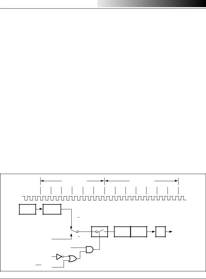
Mode 0:
Both Timers in Mode 0 are 8-bit Counters with a divide-by-32 prescaler. Figure 8 shows the Mode 0 operation as it applies to Timer 1.
In this mode, the Timer register is configured as a 13-bit register. As the count rolls over from all 1s to all 0s, it sets the Timer interrupt flag TF1. The counted input is enabled to the Timer when TR1 = 1 and either GATE = 0 or INT1 = 1. Setting GATE = 1 allows the Timer to be controlled by external input INT1, to facilitate pulse width measurements. TR1 is a control bit in the Special Function Register TCON. Gate is in TMOD.
The 13-bit register consists of all eight bits of TH1 and the lower five bits of TL1. The upper three bits of TL1 are indeterminate and should be ignored. Setting the run flag (TR1) does not clear the registers.
Mode 0 operation is the same for Timer 0 as for Timer 1, except that TR0, TF0 and INT0 replace the corresponding Timer 1 signals in Figure 8. There are two different GATE bits, one for Timer 1 (TMOD.7) and one for Timer 0 (TMOD.3).
|
|
|
ONE MACHINE |
|
|
|
|
ONE MACHINE |
|
|
|||
|
|
|
CYCLE |
|
|
|
|
|
CYCLE |
|
|
|
|
|
S1 |
S2 |
S3 |
S4 |
S5 |
S6 |
S1 |
S2 |
S3 |
S4 |
S5 |
S6 |
S1 |
OSC |
P1 P2 P1 P2 P1 P2 P1 P2 P1 P2 P1 P2 P1 P2 P1 P2 P1 P2 |
P1 P2 P1 P2 |
P1 P2 |
P1 P2 |
|||||||||
|
|
|
|
|
|
|
|
|
|
|
|
|
|
(XTAL2) |
|
|
|
|
|
|
|
|
|
|
|
|
|
OSC |
DIVIDE 12 |
|
|
|
|
|
|
|
|
|
|
|
|
|
|
|
|
C/T = 0 |
|
|
|
|
|
|
|
|
|
|
|
|
|
|
|
|
|
TL1 |
|
TH1 |
|
TF1 |
INTERRUPT |
|
|
|
|
|
|
|
|
(5 BITS) |
(8 BITS) |
|
|||
|
|
|
|
|
|
|
|
|
|
|
|||
|
T1 PIN |
|
|
C/T = 1 |
|
|
|
|
|
|
|
|
|
|
|
|
|
|
|
|
CONTROL |
|
|
|
|
|
|
|
|
|
TR1 |
|
|
|
|
|
|
|
|
|
|
|
GATE |
|
|
|
|
|
|
|
|
|
|
|
|
|
INT1 PIN |
|
|
|
|
|
|
|
|
|
|
|
|
|
|
Figure 8. Timer/Counter 1 Mode 0: 13-Bit Counter |
|
|
|
||||||||
Integrated Silicon Solution, Inc. — 1-800-379-4774 |
15 |
MC013-1C 11/21/98
 Loading...