

Page 1

Intel® Carrier Grade Server
TIGPT1U
Technical Product Specification
Revision 1.0
June, 2004
Enterprise Platforms & Services Division
Intel Secret
Page 2
Revision History Intel® Carrier Grade Server TIGPT1U TPS
Revision History
Date
June 2004 1.0 Initial release
Revision
Number
Modifications
Disclaimers
THIS SPECIFICATION IS PROVIDED "AS IS" WITH NO WARRANTIES WHATSOEVER, INCLUDING
ANY WARRANTY OF MERCHANTABILITY, NONINFRINGEMENT, FITNESS FOR ANY PARTICULAR
PURPOSE, OR ANY WARRANTY OTHERWISE ARISING OUT OF ANY PROPOSAL, SPECIFICATION
OR SAMPLE. Intel disclaims all liability, including liability for infringement of any proprietary rights,
relating to use of information in this specification. No license, express or implied, by estoppel or
otherwise, to any intellectual property rights is granted herein.
The Intel
may cause the product to deviate from published specifications. Current characterized errata are
available on request.
This document is an intermediate draft for comment only and is subject to change without notice. Readers
should not design products based on this document.
2
I
C is a two-wire communications bus/protocol developed by Philips. SMBus is a subset of the I2C
bus/protocol and was developed by Intel. Implementations of the I
bus/protocol may require licenses from various entities, including Philips Electronics N.V. and North
American Philips Corporation.
®
Carrier Grader Server TIGPT1U may contain design defects or errors known as errata which
2
C bus/protocol or the SMBus
Copyright © Intel Corporation 2004.
*Other brands and names are the property of their respective owners.
Intel Secret Revision 1.0
ii
Page 3

Intel® Carrier Grade Server TIGPT1U TPS Table of Contents
Table of Contents
1. Introduction ............................................................................................................. 1
1.1 Document Structure and Outline.................................................................. 1
2. System Overview .................................................................................................... 2
2.1 System Features.......................................................................................... 2
2.2 Chapter Structure and Outline...................................................................... 3
2.3 Introduction .................................................................................................. 4
2.4 External Chassis Features........................................................................... 8
2.4.1 Front View of Chassis .................................................................................. 8
2.4.2 Front Panel .................................................................................................. 8
2.4.3 Chassis Peripheral Bay and Hot-Plug SCSI Hard Drive Bays.................... 10
2.4.4 Rear View of Chassis................................................................................. 13
2.5 Internal Chassis Features .......................................................................... 15
2.5.1 Telecom SE7210TP1-E Server Baseboard ............................................... 15
2.5.2 Full-Height, Full-Length PCI Adapter Subsystem....................................... 16
2.5.3 Power Subsystem ...................................................................................... 17
2.5.4 Cooling Subsystem .................................................................................... 18
2.6 Server Management .................................................................................. 19
2.6.1 Baseboard Management Controller ........................................................... 19
2.7 Specifications............................................................................................. 20
2.7.1 Environmental Specifications ..................................................................... 20
2.7.2 Physical Specifications .............................................................................. 21
3. Cables and Connectors ........................................................................................ 22
3.1 Chapter Structure and Outline ................................................................... 22
3.2 Interconnect Block Diagram....................................................................... 23
3.3 Cable and Interconnect Descriptions ......................................................... 24
3.4 Exteranly-Accessible Interconnects ........................................................... 25
3.4.1 Keyboard and Mouse Ports........................................................................ 25
3.4.2 Serial Ports ................................................................................................ 26
3.4.3 Video Port .................................................................................................. 27
3.4.4 Universal Serial Bus (USB) Interface ......................................................... 27
3.4.5 Ethernet Connector.................................................................................... 28
Revision 1.0 Intel Secret
iii
Page 4

Table of Contents Intel® Carrier Grade Server TIGPT1U TPS
3.4.6 Telco Alarms Connector............................................................................. 28
3.4.7 AC Power Input for AC-Input Power Supply............................................... 28
3.4.8 DC Power Input for DC-Input Power Supply .............................................. 29
4. Extended Front Panel System Board .................................................................. 30
4.1 Features..................................................................................................... 30
4.2 Chapter Structure and Outline ................................................................... 30
4.3 Introduction ................................................................................................ 31
4.4 Functional Description of Front Panel Switches, LEDs, and Relays .......... 31
4.4.1 Front Panel Switches ................................................................................. 31
4.4.2 Front Panel LEDs....................................................................................... 32
4.4.3 System Status LEDs .................................................................................. 32
4.4.4 System Fault LEDs .................................................................................... 33
4.4.5 LED Color Selection................................................................................... 33
4.4.6 System Fault Relays .................................................................................. 34
4.4.7 Server Management Bus (SMBus) Interface.............................................. 34
4.5 Connector Information ............................................................................... 35
4.5.1 Extended Front Panel Board USB Connector Pinout................................. 37
4.5.2 Extended Front Panel Board uProcessor Power Connector Pinout ........... 37
4.5.3 Extended Front Panel Board Front Panel Connector Pinout...................... 38
4.5.4 Extended Front Panel Board Midplane Connector Pinout.......................... 38
4.5.5 Extended Front Panel Board Power/Signal Connector Pinout ................... 39
4.5.6 Extended Front Panel Board Alarm/COM2 Connector Pinout.................... 39
4.5.7 Extended Front Panel Board Baseboard Power Connector Pinout............ 40
4.5.8 Extended Front Panel Board COM2/USB Connector Pinout ..................... 40
4.5.9 Extended Front Panel Board NEBS Riser Power Connector Pinout .......... 40
4.6 SCSI Power Subsystem............................................................................. 41
4.6.1 SCSI Drive Power Control.......................................................................... 41
4.6.2 Internal SCSI Drive Power Switching......................................................... 41
4.6.3 SCSI Drive Status LEDs ............................................................................ 42
4.7 Specifications............................................................................................. 43
4.7.1 Electrical Specifications ............................................................................. 43
5. Power Interconnect System Board...................................................................... 44
5.1 Features..................................................................................................... 44
Intel Secret Revision 1.0
iv
Page 5

Intel® Carrier Grade Server TIGPT1U TPS Table of Contents
5.2 Chapter Structure and Outline ................................................................... 44
5.3 Functional Description of Power Interconnect System Board .................... 44
5.4 Connector Description ............................................................................... 45
5.4.1 Connector Mating to the Power Supply Pinout........................................... 45
5.4.2 Connector Mating to the Extended Front Panel System Board Pinout....... 46
6. NEBS 3.3 V Riser Board........................................................................................ 47
6.1 Chapter Structure and Outline ................................................................... 47
6.2 Functional Description ............................................................................... 47
6.3 Connector Interface ................................................................................... 48
6.3.1 NEBS Riser Power Connector Pinout ........................................................ 50
6.4 Electrical Specification ............................................................................... 51
7. Midplane Board ..................................................................................................... 52
7.1 Chapter Structure and Outline ................................................................... 52
7.2 Introduction ................................................................................................ 52
7.3 Functional Description ............................................................................... 53
7.3.1 Midplane System Board SCSI Subsystem Block Diagram......................... 53
7.3.2 SCSI Bus ................................................................................................... 54
7.3.3 SCA2 Connector Interlocks........................................................................ 54
7.3.4 Signal Descriptions .................................................................................... 54
7.4 Connector Interface ................................................................................... 56
7.4.1 Midplane Power/Signal Connector Pinout.................................................. 57
7.4.2 Midplane SCSl Connector Pinout and SCSI ID settings ............................ 57
7.5 Specifications............................................................................................. 57
7.5.1 Electrical Specifications ............................................................................. 57
8. DC Power Subsystem ........................................................................................... 58
8.1 Features..................................................................................................... 58
8.2 Chapter Structure and Outline ................................................................... 58
8.3 Introduction ................................................................................................ 58
8.4 Mechanical Interface.................................................................................. 59
8.4.1 Power Supply Cage Mechanical Outline.................................................... 59
8.4.2 DC Input Terminal Block Connector........................................................... 60
8.4.3 DC Output Connector ................................................................................ 61
8.4.4 Power Supply Module LED Indicators........................................................ 63
Revision 1.0 Intel Secret
v
Page 6

Table of Contents Intel® Carrier Grade Server TIGPT1U TPS
8.5 Electrical Requirements ............................................................................. 63
8.5.1 DC Input Voltage Specification .................................................................. 63
8.5.2 Dual DC Input ............................................................................................ 63
8.5.3 DC Output Current Specifications .............................................................. 64
9. AC Power Subsystem ........................................................................................... 65
9.1 Features..................................................................................................... 65
9.2 Chapter Structure and Outline ................................................................... 65
9.3 Introduction ................................................................................................ 65
9.4 Mechanical Interface.................................................................................. 66
9.4.1 Power Supply Cage Mechanical Outline.................................................... 66
9.4.2 AC Input Connector ................................................................................... 66
9.4.3 DC Output Connector ................................................................................ 67
9.4.4 Power Supply Module LED Indicators........................................................ 69
9.5 Electrical Requirements ............................................................................. 69
9.5.1 AC Input Voltage Specification................................................................... 69
10. Regulatory Specifications .................................................................................... 70
10.1 Safety Compliance..................................................................................... 70
10.2 Electromagnetic Compatibility.................................................................... 70
10.3 CE Mark..................................................................................................... 70
10.4 NEBS Compliance (DC Input Only) ........................................................... 71
10.5 ETSI Standards Compliance (DC Input Only)............................................ 71
Appendix A: Glossary................................................................................................. 72
Appendix B: Reference Documents .......................................................................... 76
Intel Secret Revision 1.0
vi
Page 7

Intel® Carrier Grade Server TIGPT1U TPS List of Figures
List of Figures
Figure 2-1. Intel® Carrier Grade Server TIGPT1U ........................................................... 4
Figure 2-2. Intel® Carrier Grade Server TIGPT1U (shown with top covers and bezel
removed) ................................................................................................................... 5
Figure 2-3. Intel® Carrier Grade Server TIGPT1U Block Diagram ................................... 7
Figure 2-4. Front View of System.................................................................................... 8
Figure 2-5. Front View of System (shown with bezel removed) ...................................... 8
Figure 2-6. Front Panel Details ....................................................................................... 9
Figure 2-7. Chassis Peripheral Bay and Hard Drive Bays............................................. 10
Figure 2-8. Peripheral Drive Bay ................................................................................... 11
Figure 2-9. Drive Carrier Assembly ............................................................................... 11
Figure 2-10. SCSI Hard Drive Bays .............................................................................. 12
Figure 2-11. SCSI Hard Drive Carrier............................................................................ 13
Figure 2-12. Rear View of System ................................................................................ 13
Figure 2-13. Telecom SE7210TP1-E Server Baseboard Block Diagram ...................... 15
Figure 2-14. Full-Height, Full-Length PCI Adapter Subsystem...................................... 17
Figure 2-15. System Fan Assemblies............................................................................ 18
Figure 3-1. Intel® Carrier Grade Server TIGPT1U Interconnect Block Diagram ........... 23
Figure 3-2. Telco Alarms Connector.............................................................................. 28
Figure 3-3. AC Power Input Connector ......................................................................... 29
Figure 3-4. DC Power Input Connector ......................................................................... 29
Figure 3-5. Terminal Lug ............................................................................................... 29
Figure 4-1. Extended Front Panel Board....................................................................... 31
Figure 4-2. Extended Front Panel Board Connector Location....................................... 36
Figure 5-1. Physical Layout of Power Interconnect System Board................................ 44
Figure 6-1. Physical Layout of NEBS 3.3 V Riser Board ............................................... 48
Figure 7-1. Midplane System Board SCSI Subsystem Block Diagram.......................... 53
Figure 7-2. Extended Front Panel Board Connector Location....................................... 56
Figure 8-1. Power Subsystem Enclosure Outline Drawing............................................ 59
Figure 8-2. DC Input Terminal Block ............................................................................. 60
Figure 8-3. Terminal Lug ............................................................................................... 60
Figure 8-4. Terminal Block Polarity .............................................................................. 60
Revision 1.0 Intel Secret
vii
Page 8

List of Figures Intel® Carrier Grade Server TIGPT1U TPS
Figure 8-5. Edge Finger Layout..................................................................................... 62
Figure 9-1. Power Subsystem Enclosure Outline Drawing............................................ 66
Figure 9-2. Edge Finger Layout..................................................................................... 68
Intel Secret Revision 1.0
viii
Page 9

Intel® Carrier Grade Server TIGPT1U TPS List of Tables
List of Tables
Table 2-1. Intel® Carrier Grade Server TIGPT1U Feature List......................................... 2
Table 2-2. Front Panel Features ..................................................................................... 9
Table 2-3. System Features - Rear ............................................................................... 14
Table 2-4. Environmental Specifications Summary....................................................... 20
Table 2-5. Dimensions and Weight ............................................................................... 21
Table 3-1. System Interconnect Descriptions................................................................ 24
Table 3-2. Keyboard/Mouse PS/2 Connector Pin Out (J9A1) ....................................... 25
Table 3-3. COM1: 9-pin Serial A Port Pin Out (J8A1) ................................................... 26
Table 3-4. COM2: Serial Port Connector on Front Panel .............................................. 26
Table 3-5. Video Connector .......................................................................................... 27
Table 3-6. Single USB Connector ................................................................................. 27
Table 3-7. Magjack Connector (RJ45, 10/100/1000) Pin Out (J5A1, J6A2) .................. 28
Table 3-8. Telco Alarms Connector............................................................................... 28
Table 4-1. Front Panel Switch Description .................................................................... 31
Table 4-2. LED Specifications ....................................................................................... 32
Table 4-3. Front Panel System Status LED Description................................................ 32
Table 4-4. Front Panel System Fault LED Description.................................................. 33
Table 4-5. LED Color Selection..................................................................................... 33
Table 4-6. Alarms SMBus I/O Mapping......................................................................... 34
Table 4-7. SCSI SMBus I/O Mapping............................................................................ 35
Table 4-8. Extended Front Panel System Board Connector Information....................... 35
Table 4-9. Connector Housing Information.................................................................... 36
Table 4-10. 8-pin (1 x 8) USB J2G1 Connector............................................................. 37
Table 4-11. 8-pin (2 x 4) uP Power J5A1 Connector..................................................... 37
Table 4-12. 34-pin (2 x 17) Front Panel J8A1 Connector .............................................. 38
Table 4-13. 12-pin (2 x 6) Mid-Plane J1E1 Connector .................................................. 38
Table 4-14. 10-pin (2 x 5) Power/Signal J9A1 Connector ............................................. 39
Table 4-15. 24-pin (2 x 12) Alarm/COM2 J9B1 Connector............................................ 39
Table 4-16. 20-pin (2 x 10) Baseboard Power J10A1 Connector .................................. 40
Table 4-17. 16-pin Baseboard Power J1A1 Connector ................................................. 40
Revision 1.0 Intel Secret
ix
Page 10

List of Tables Intel® Carrier Grade Server TIGPT1U TPS
Table 4-18. 3-pin (1 x 3) NEBS Riser Power J3E1 Connector ...................................... 40
Table 4-19. LED Activity Definitions .............................................................................. 42
Table 4-20. Maximum Power Requirements (mA) ........................................................ 43
Table 5-1. 2 x 31 Connector Pinout to 250 Watt Power Supply .................................... 45
Table 5-2. 2 x 31 Connector Pinout to Extended Front Panel System Board................ 46
Table 6-1. Riser Card Slot Pin-out Common Signals .................................................... 48
Table 6-2. PCI Card Connector Signals ........................................................................ 49
Table 6-3. 3-pin (1 x 3) NEBS Riser Power J1A1 Connector ........................................ 50
Table 7-1. LVD SCSI Bus Signals – J2L1, J4A1, J8A1................................................. 55
Table 7-2. Extended Front Panel System Board Connector Information....................... 56
Table 7-3. Connector Housing Information.................................................................... 57
Table 7-4. 12-pin (2 x 6) Midplane J9L1 Connector ...................................................... 57
Table 7-5. MPB Power Requirements ........................................................................... 57
Table 8-1. 250 Watt DC-input Power Supply DC Output Ratings.................................. 58
Table 8-2. Edge Finger Pinout ...................................................................................... 61
Table 8-3. LED Indicators.............................................................................................. 63
Table 8-4. DC Input Rating............................................................................................ 63
Table 8-5. 250 W Load Ratings..................................................................................... 64
Table 9-1. 250 Watt AC-input Power Supply DC Output Ratings.................................. 65
Table 9-2. Edge Finger Pinout ...................................................................................... 67
Table 9-3. LED Indicators.............................................................................................. 69
Table 9-4. AC Input Rating............................................................................................ 69
Intel Secret Revision 1.0
x
Page 11

Intel® Carrier Grade Server TIGPT1U TPS Introduction
1. Introduction
This document provides an overview of the Intel
Industrial Grade Prescott 1U (1.75”) high) and includes information on chassis hardware,
cables, connectors, SE7210TP1-E System Baseboard, system boards, power subsystem, and
regulatory requirements.
®
Carrier Grade Server TIGPT1U (Telecom
1.1 Document Structure and Outline
This document is organized into the following chapters:
Chapter 1: Introduction
Provides an overview of this document.
Chapter 2: System Overview
Provides an overview of the Intel
Chapter 3: Cables and Connectors
Describes the cables and connectors used to interconnect the system
board set and the Intel
Chapter 4: Extended Front Panel System Board
Describes the specifications of the extended front panel system board.
Chapter 5: Power Interconnect System Board
Describes the specifications of the power interconnect system board.
®
TIGPT1U components.
®
TIGPT1U server chassis hardware.
Chapter 6: NEBS 3.3 V Riser Board
Describes the specifications of the Network Equipment Building
Specifications (NEBS) 3.3 V riser board.
Chapter 7: Midplane Board
Describes the specifications of the midplane board.
Chapter 8: DC Power Subsystem
Describes the specifications of the DC power subsystem.
Chapter 9: AC Power Subsystem
Describes the specifications of the AC power subsystem.
Chapter 10: Regulatory Specifications
Describes system compliance to regulatory specifications.
Revision 1.0 Intel Secret 1
Page 12

System Overview Intel® Carrier Grade Server TIGPT1U TPS
2. System Overview
This chapter describes the features of the Intel® Carrier Grade Server TIGPT1U chassis.
2.1 System Features
Table 2-1 provides a list and brief description of the features of the Intel® Carrier Grade Server
TIGPT1U.
Table 2-1. Intel® Carrier Grade Server TIGPT1U Feature List
Feature Description
Compact, high-density system Rack-mount server with a height of 1 U (1.75 inches) and a depth of 20.0 inches
Configuration flexibility Single processor capability in low profile and cost/value effective packaging
Stand-alone system
Intel® Pentium® 4 Processor with hyper-threading technology at 3.0 GHz
Serviceability Front access to hot swap disk drives
Availability Integrated HostRAID™ ready to provide RAID 1 capability using two hot-swap
Small Computer System Interface (SCSI) disk drives.
Manageability Remote management
Emergency management port (Serial and LAN)
IPMI 1.5 compliant
Remote diagnostics support
System-level scalability 4 GB DDR333/DDR400 unbuffered 184-pin DDR SDRAM DIMM memory
support
Single Intel
1 Full Height Full Length 3.3 V/Universal 64-bit x 66 MHz PCI-X Slots
2 internal hot-swap SCSI disk drives (SCA support)
1 Low Profile CD-ROM
Front panel Power switch
Reset switch
NMI switch
ID switch
Main power LED
HDD activity LED
NIC activity LED
ID LED
®
Pentium® 4 Processor support
Hard Drive 0 Fault LED
Hard Drive 1 Fault LED
Telco power alarm fault LED/Relay
Telco critical alarm fault LED/Relay
Telco major alarm fault LED/Relay
Telco minor alarm fault LED/Relay
Revision 1.0
2
Page 13

Intel® Carrier Grade Server TIGPT1U TPS System Overview
2.2 Chapter Structure and Outline
This chapter is organized into the following sections. The content of each section is
summarized as follows.
Section 2.3: Introduction
Provides an overview and block diagram of the Intel
®
Carrier Grade
Server TIGPT1U.
Section 2.4: External Chassis Features
Describes features of the Intel
®
Carrier Grade Server TIGPT1U chassis in
detail (buttons, switches, bezel, etc.).
Section 2.5: Internal Chassis Features
Provides an overview of the components of the Intel
®
Carrier Grade
Server TIGPT1U.
Section 2.6: Server Management
Describes the server management features of the Intel
®
Carrier Grade
Server TIGPT1U.
Section 2.7: Specifications
Summarizes the environmental and physical specifications of the Intel
®
Carrier Grade Server TIGPT1U.
Revision 1.0
3
Page 14
System Overview Intel® Carrier Grade Server TIGPT1U TPS
2.3 Introduction
The Intel® TIGPT1U is a compact, high-density, rack mount server system with support for one
®
Intel
Pentium® 4 Processor and 4 GB DDR266/DDR333/DDR400 unbuffered 184-pin DDR
SDRAM DIMM memory. The Intel
drives and remote management. The scalable architecture of the Intel
variety of operating systems (OS).
Figure 2-1 shows an isometric view of the system.
Figure 2-2 shows the system with the top covers and the front bezel removed.
®
TIGPT1U high availability features include hot swap disk
®
TIGPT1U supports a
Figure 2-1. Intel® Carrier Grade Server TIGPT1U
The Intel® TIGPT1U uses the SE7210TP1-E system baseboard, which contains connectors for
installing one Intel
DIMM slots and supports up to 4 GB error checking and correcting (ECC) unbuffered
Synchronous Dynamic Random Access Memory (SDRAM). The SE7210TP1-E system
baseboard also contains 1 PCI slots (implemented via riser cards), input/output (I/O) ports and
various controllers.
®
Pentium® 4 Processor utilizing the uPGA478 socket. The baseboard has 4
Revision 1.0
4
Page 15
Intel® Carrier Grade Server TIGPT1U TPS System Overview
D
E
F
G
H
I
Figure 2-2. Intel
C
A
M
L
®
Carrier Grade Server TIGPT1U (shown with top covers and bezel removed)
B
K
J
A. Power Supply H. SCSI Hard Disk Drive Bays
B. PCI card bracket (full-length) I. Peripheral Bay (CDROM or DVD)
C. Riser card assembly (full-length) J. Front Panel LEDs and Switches
D. SE7210TP1-E Server Baseboard K. COM2/USB Front Panel Connector
E. System Memory L. Extended Front Panel System Board
F. System Fans M. Power Interconnect System Board
G. Midplane System Board
The SE7210TP1-E system baseboard is mounted horizontally toward the rear of the chassis
behind the system fan array.
Revision 1.0
5
Page 16

System Overview Intel® Carrier Grade Server TIGPT1U TPS
Up to two 1.0” Ultra-320 SCSI technology hard drives can be mounted in the hot swap drive bays,
which are located in the bottom front of the chassis. The front bezel needs to be removed to
access the hot swap drive trays when installing or removing them from the hot
swap drive bays.
Figure 2-2 shows the location of the two hot swap drive bays.
A slim-line CD-ROM drive can also be mounted in the system above the two hot swap drive
bays.
System boards include the extended front panel board, the power supply interface board, and
the SCSI hot swap backplane board. The extended front panel board is located in the front left
of the chassis, the power supply interface board is located in the mid left of the chassis, and the
SCSI hot swap backplane is located in the mid center and right of the chassis.
The 250 W power supply is mounted at the left-rear of the chassis. Two power supply options
are available, one with AC-input and one with DC-input.
The system contains a fan array consisting of two 40 x 48 mm fans and one 40 x 28 mm fans to
cool the SE7210TP1-E System Baseboard and other components. The fans are installed
directly behind the drive bays and are located in front of the baseboard. Another 40 x 28 mm
fan is located to the left of the hot swap drive bays and is used to cool the PCI adapter and left
side of the SE7210TP1-E System Baseboard. Individual fan connectors are located on the
system baseboard.
The front bezel can be customized to meet OEM industrial design requirements. The bezel
design allows adequate airflow to cool the system components. The front bezel is removed to
access the drive bay.
Figure 2-3 shows a block diagram of the Intel
®
Carrier Grade Server TIGPT1U with
interconnections.
Revision 1.0
6
Page 17
Intel® Carrier Grade Server TIGPT1U TPS System Overview
250 W Power Supply
(AC-input or DC-input)
Interconnect Board
LAN 2 82541 Gb E/N
VGA RAGE XL
87431
mBMC
PCI Slot 1
Full Height/Full Length
5V Riser PCI-X 64/66
PCI Riser Slot 1
PCI-X 64/66
SCSI AIC-7901
USB1/2/3 (Back)
USB 4 (Front)
ATA/100 (IDE)
Front Panel
Front Panel Baseboard Pwr
uP
Pwr
PCI-X
64/66
6300ESB
I/O Controller
Fan 6
Winbond
W83627HF-AW
Super I/O
PCI
LPC Bus
64/33
Hub
Baseboard Pwr
COM2/Alarm
82802
AC
8 Mb
F/W
Hub
Flash
BIOS
CSA
HUB Interface
Fan 1
Alarm Out
PS2 Keyboard/Mouse
COM1 (Back)
COM2 (Front)
LAN1 82547 Gb E/N
Pentium 4
uPGA478
Front Side Bus
800 MB/s
827210 Memory
Controller Hub
Baseboard
CPU VRM
Channel A
Channel B
DDR 400/333
System
uP
Pwr
2GB DDR SDRAM
Fan 5Fan 4Fan 3 Fan 2
USB 4
Extended Front Panel Board
Push Buttons
C
U
S
B
Pwr|Rst
O
M
2
NMI|ID
System Fault LEDs
Crt|Mjr|Mnr|Pwr
Activity/ID LEDs
ID|NIC|On|Disk1|Disk0
Figure 2-3. Intel® Carrier Grade Server TIGPT1U Block Diagram
MP
Pwr
CDROM/DVD Drive Bay
Note: The CDROM/DVD
Drive is positioned above
SCSI Hard Drive Bay 1
Sig 2x20, Pwr 1x2
1/2"
CDROM/DVD
SCSI LVD Term
MidPlane Board
MP
Pwr
SCSI SCA Conn 80pin
SCSI SCA Conn 80pin
SCSI Hard Drive 1
Hot Plug Drive Assembly
Consists of:
1. SCA SCSI Disk Drive
2. Drive Carrier
SCSI SCA Conn 80pin
SCSI SCA Conn 80pin
SCSI Hard Drive 1
Hot Plug Drive Assembly
Consists of:
1. SCA SCSI Disk Drive
2. Drive Carrier
SCSI Hard Drive Bay 1 SCSI Hard Drive Bay 0
SCSI BB Conn
68 Pin Wide U-320 SCSI Bus
Revision 1.0
7
Page 18
System Overview Intel® Carrier Grade Server TIGPT1U TPS
2.4 External Chassis Features
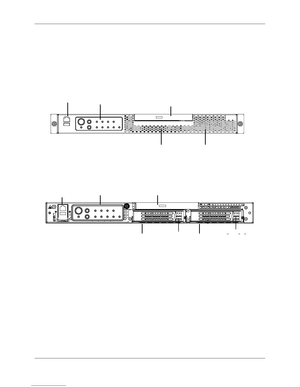
2.4.1 Front View of Chassis
Figure 2-4 shows the front view of the system. Figure 2-5 shows the front view of the system
with the front bezel removed. Removing the front bezel provides access to the two hot-plug
hard drive bays.
Both areas are described in detail in the following sections.
RJ45 COM2 and
USB Connectors
RJ45 COM2 and
Dual USB Connectors
Front Panel Control Switches
and Status LEDs
Figure 2-4. Front View of System
Front Panel Control
Switches and Status LEDs
Peripheral Bay
Drive Bay 2 Drive Bay 1
Peripheral Bay
Drive Bay 2 Drive Bay 1
Figure 2-5. Front View of System (shown with bezel removed)
Drive Bay 2 Handle Drive Bay 1 Handle
2.4.2 Front Panel
The front panel features are shown in Figure 2-6 and described in Table 2-2. All front panel
control switches and status LEDs are contained on the front panel system board. Please refer to
Section 5 Front Panel System Board for a detailed description of the control switches and status
LEDs contained on the Front Panel.
Revision 1.0
8
Page 19
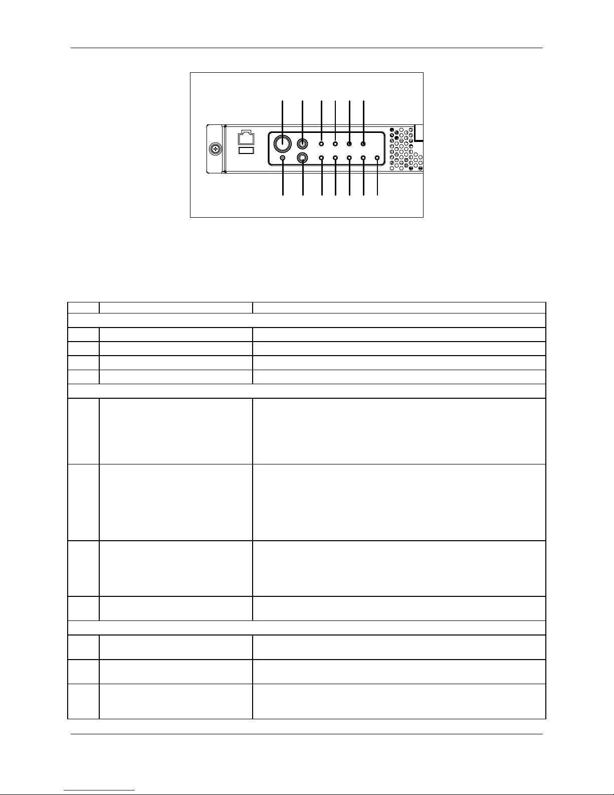
Intel® Carrier Grade Server TIGPT1U TPS System Overview
ABCDEF
GHIJKLM
Figure 2-6. Front Panel Details
Table 2-2. Front Panel Features
Item Feature Description
Front Panel Switches
A Power switch Toggles the system power
B Reset switch Resets the system
L ID switch Toggles system ID LED
M NMI switch Assert NMI to baseboard
Front Panel Alarm LEDs and Relays
C Critical (amber) When continuously lit, indicates the presence of a Critical System
Fault. A critical system fault is an error or event that is detected by the
system with a fatal impact to the system. In this case, the system
cannot continue to operate. An example could be the loss of a large
section of memory, or other corruption, that renders the system not
operational. The front panel critical alarm relay will be engaged.
D Major (amber) When continuously lit, indicates the presence of a Major System Fault.
A major system fault is an error or event that is detected by the system
that has discernable impact to system operation. In this case, the
system can continue to operate but in a “degraded” fashion (reduced
performance or loss of non-fatal feature reduction). An example could
be the loss of one of two mirrored disks. The front panel major alarm
relay will be engaged.
E Minor (amber) When continuously lit, indicates the presence of a Minor System Fault.
A minor system fault is an error or event that is detected by the system
but has little impact to actual system operation. An example would be
a correctable ECC error. The front panel minor alarm relay will be
engaged.
F Power (amber) When continuously lit, indicates the presence of a Power System
Fault. The front panel power alarm relay will be engaged.
Front Panel Status LEDs
G Disk 1 Activity/Fault LED
(green/amber)
H Disk 2 Activity/Fault LED
(green/amber)
I Main power LED (green) When continuously lit, indicates the presence of DC power in the
Indicates disk 1 SCSI hard drive activity when green, or a disk 1 SCSI
hard drive fault when amber
Indicates disk 2 SCSI hard drive activity when green, or a disk 2 SCSI
hard drive fault when amber
server. The LED goes out when the power is turned off or the power
source is disrupted.
Revision 1.0
9
Page 20
System Overview Intel® Carrier Grade Server TIGPT1U TPS
Item Feature Description
J NIC0/NIC1 activity LED (green) Indicates activity on either NIC0 or NIC1
K System ID LED (white) Continuously lit when activated by (1) software command to extended
front panel board or (2) by the front panel ID switch
2.4.3 Chassis Peripheral Bay and Hot-Plug SCSI Hard Drive Bays
The Intel® TIGPT1U server chassis provides two hot-swap SCSI hard drive bays at the front of
the chassis, along with a peripheral bay that supports either a fixed CDROM Drive (read-only or
read/write, or a fixed DVD Drive. Both hot-plug SCSI hard drive bays may be populated with a
3.5” SCSI Single Connector Attachment (SCA) hard disk drive mounted in a SCSI drive carrier.
The SCSI ID for each hard drive position is hardwired on the midplane board, so the use of
jumper(s) to select a unique SCSI ID is not necessary. Hard disk drive position 1 is hardwired to
SCSI ID 0 on the SCSI bus and hard disk drive position 2 is hardwired to SCSI ID 1 on the SCSI
bus.
A
C
A. Hard drive bay 1 (SCSI ID 0)
B. Hard drive bay 2 (SCSI ID 1)
C. Peripheral drive bay
D. CD-ROM drive or DVD drive mounted in a peripheral carrier
E. Hard disk drive module
B
D
E
Figure 2-7. Chassis Peripheral Bay and Hard Drive Bays
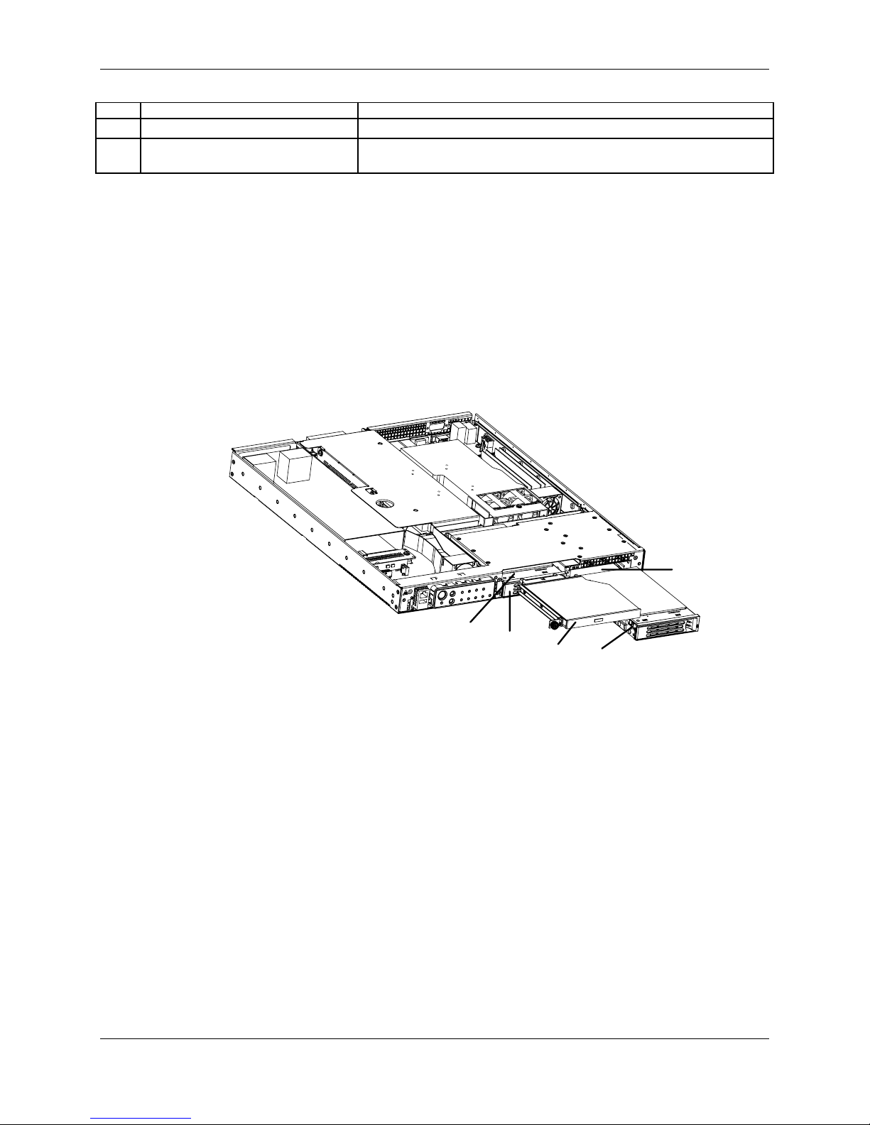
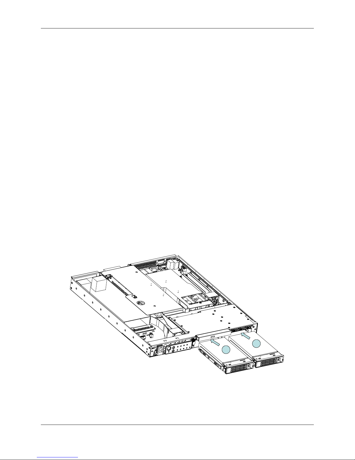
2.4.3.1 Peripheral Drive Bay
The peripheral bay supports either a CDROM drive or a DVD drive.
The peripheral drive carrier assembly can be configured with either a 0.5” (12.7 mm) slim-line
CD-ROM or DVD drive. The install sequence is (1) slide the peripheral drive carrier into the
peripheral drive bay, (2) tighten the thumb screw to secure the peripheral drive carrier to the
chassis, and (3) connect the IDE and power cables to the interconnect board.
Note: A floppy drive cannot be installed in the system using the peripheral drive bay. If a floppy
drive is needed, it will be necessary to use a Universal Serial Bus (USB) floppy and connect it to
Revision 1.0
10
Page 21
Intel® Carrier Grade Server TIGPT1U TPS System Overview
the USB connection on the front of the unit or one of the USB connections on the back of the
unit.
3
2
1
Figure 2-8. Peripheral Drive Bay
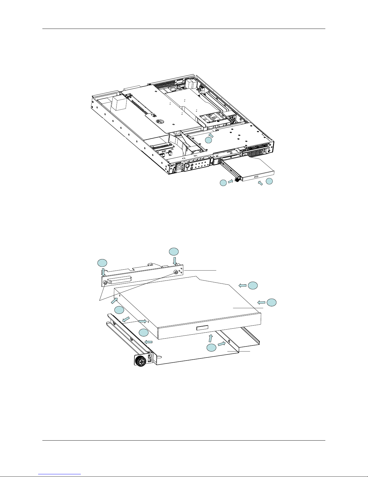
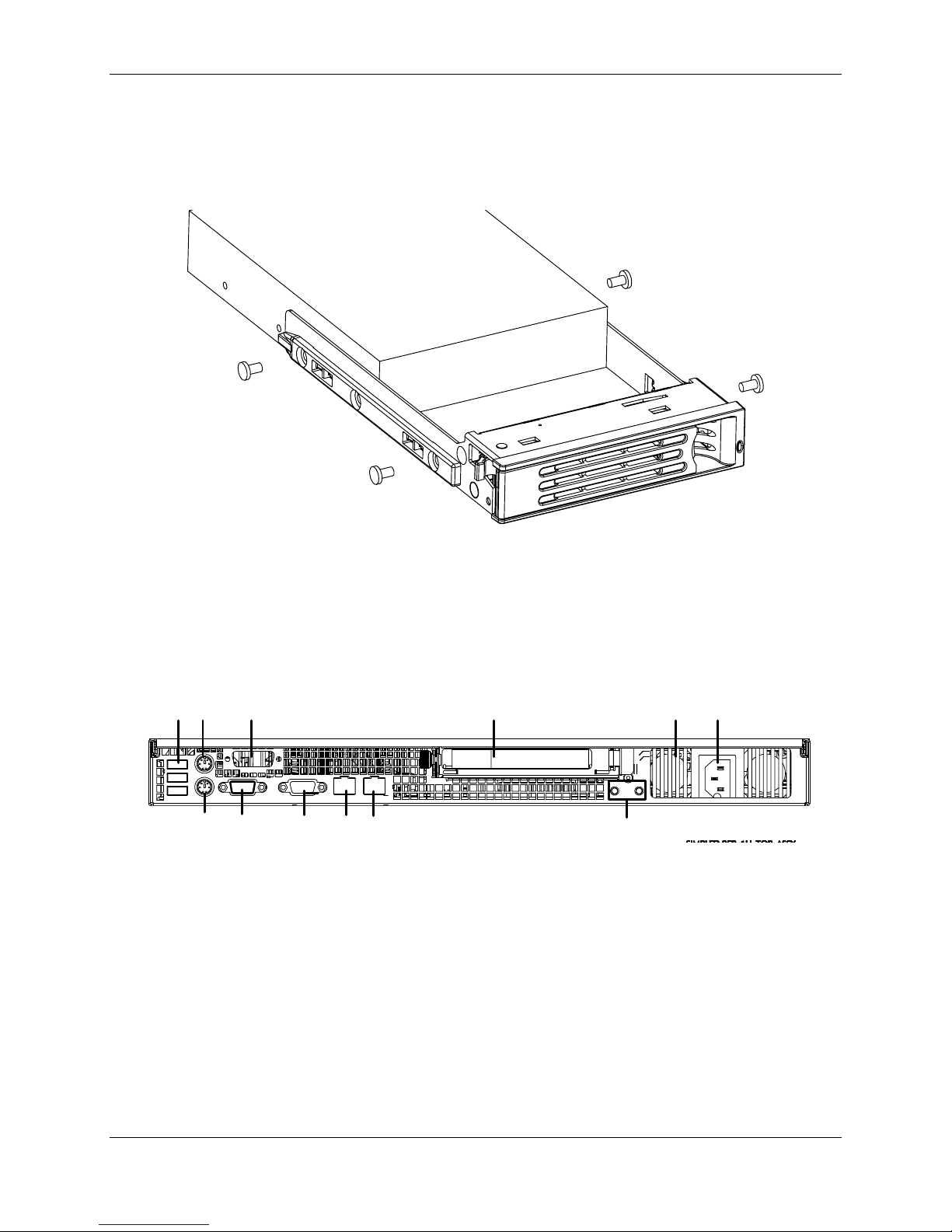
2.4.3.1.1 Peripheral Drive Carrier Assembly
The CDROM drive or DVD drive is installed in the drive carrier assembly before installing it into
the system. An exploded view of the drive carrier assembly is shown in the following figure:
1
1
C
2
D
3
3
2
A
2
B
Revision 1.0
A. Drive carrier metal housing
B. CD-ROM or DVD Drive
C. Interface Board
D. Two screws to connect interface board to CD-ROM or DVD drive
Figure 2-9. Drive Carrier Assembly
11
Page 22
System Overview Intel® Carrier Grade Server TIGPT1U TPS
Prior to installing the drive in the system, (1) the interface board is connected to the back of the
drive and secured with two 8mm screws. The drive is then installed in the drive carrier metal
housing by holding the left side of the drive carrier in the left hand, and with the right hand
installing the right side of the drive into the right side of the drive carrier, (2) making sure to line
up the two holes in the right side of the drive with the two mounting tabs on the right side of the
drive carrier. Then, while flexing the left side of the drive carrier slightly down, (3) insert the left
side of the drive into the drive carrier, making sure to line up the two holes on the left side of the
drive with the two mounting tabs on the left side of the drive carrier. If this is done correctly, the
drive carrier will be flush with the bottom and sides of the drive, and all four mounting tabs will
be installed in the mounting holes on the drive. Observe that the right side mounting tabs are
correctly inserted into the right side mounting holes on the drive by looking at the right bottom of
the drive carrier assembly. Observe that the left side mounting tabs are correctly inserted into
the left side mounting holes on the drive by looking at the top left of the drive carrier assembly.
2.4.3.2 Hard Drive Bays
There are two hot-plug SCSI SCA hard drive bays in the system (see (1) and (2) in the drawing
below). Each hard drive bay supports a U320 SCA (single connector attach) SCSI disk drive
mounted in a drive tray. The drive tray is installed into the front of the chassis in the hard drive
bay, and then secured in place by latching the handle on the drive tray. Ultra 320 SCSI
technology (SCA interconnect) or slower hard disk drives can be installed in the hard drive bays.
The hard drive bays are designed to accept 15,000 rotations per minute (RPM) hard drives (and
below) that consume up to 18 W of power.
The SCSI ID for each hard drive position is hardwired on the midplane board, so the use of
jumper(s) to select a unique SCSI ID is not necessary. Hard disk drive position 1 is hardwired
to SCSI ID 0 on the SCSI bus and hard disk drive position 2 is hardwired to SCSI ID 1 on the
SCSI bus.
1
2
Figure 2-10. SCSI Hard Drive Bays
Revision 1.0
12
Page 23
Intel® Carrier Grade Server TIGPT1U TPS System Overview
2.4.3.2.1 Hard Drive Tray
Each hard drive used in the system must be mounted to a drive tray using four screws inserted
into the sides of the drive as shown in the figure.
Figure 2-11. SCSI Hard Drive Carrier
2.4.4 Rear View of Chassis
B
A
C
LK
H
I
J
Figure 2-12. Rear View of System
D
G
F
E
Revision 1.0
13
Page 24

System Overview Intel® Carrier Grade Server TIGPT1U TPS
Table 2-3. System Features - Rear
Item Description
A USB 1, USB 2, USB 3
B PS/2 Mouse
C DB15 Alarm Connector
D PCI card bracket (full-height)
E Power supply
F AC power input ( AC input power supply shown)
G Ground Studs (used with system with DC input power supply)
H RJ45 Network Interface Card (NIC) 2 connector
I RJ45 NIC 1 connector
J Video connector
K DB9 serial 2 port
L PS/2 Keyboard connector
Revision 1.0
14
Page 25
Intel® Carrier Grade Server TIGPT1U TPS System Overview
2.5 Internal Chassis Features
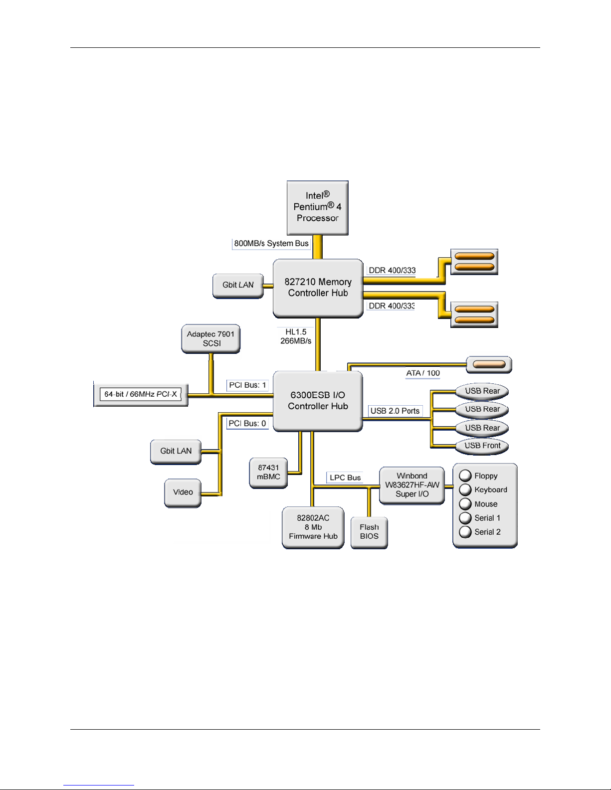
2.5.1 Telecom SE7210TP1-E Server Baseboard
The telecom SE7210TP1-E Server Baseboard is a monolithic printed circuit board that can
accept one Intel
The figure below shows the functional blocks of the telecom SE7210TP1-E Server Baseboard
and the plug-in modules that it supports.
®
Pentium® 4 Processor with hyper-threading technology in a µPGA478 socket.
Figure 2-13. Telecom SE7210TP1-E Server Baseboard Block Diagram
o Support for an Intel® Pentium® 4 Processor with hyper-threading technology in a µPGA478
socket (3.0 GHz frequency, 1 M L2 cache, 800 MHz Front Side Bus (FSB), 90 nm
manufacturing technology).
o 400/533/800 MHz FSB
o Intel
Revision 1.0
®
E7210 chipset
• Intel
• Intel
• Intel
®
®
®
827210 Memory Controller Hub (MCH)
6300ESB I/O Controller Hub (Hance Rapids)
82802AC 8 Megabit Firmware Hub (FWH)
15
Page 26

System Overview Intel® Carrier Grade Server TIGPT1U TPS
o Support for single-sided or double-sided dual inline memory module (DIMM) double-data
rate (DDR) memory providing up to 4 GB of system memory with four 184-pin DIMM sockets
®
• PC3200 (400 MHz): to run 400 MHz memory at full speed requires an Intel
Pentium® 4
Processor with 800 MHz system bus frequency.
• PC2700 (333 MHz): to run 333 MHz memory at full speed requires an Intel
®
Pentium® 4
Processor with 533 MHz system bus frequency.
®
o Intel
Note: PC2700 (333 MHZ) memory will run at 320 MHz frequency when using an Intel
Pentium
®
82547EI Platform LAN Connect (PLC) device for 10/100/1000 Mbps Ethernet LAN
®
4 Processor with 800 MHz system bus frequency.
connectivity
o Intel
®
82541EI device for 10/100/1000 Mbps Ethernet LAN connectivity
o Two independent PCI buses (one 32-bit, 33 MHz, 5 V; one 64-bit, 66 MHz, 3.3 V) with one
PCI connectors and two embedded devices:
• One PCI-X 64-bit 66-MHz PCI slots
• Integrated 2D/3D graphics controller: ATI* Rage* XL Video Controller with 8 MB of
SDRAM
• Single channel, Ultra 320 Small Computer System Interface (SCSI) Controller: Adaptec*
7901*
o Low Pin Count (LPC) bus segment with one embedded device: Winbond* W83627HF-AW
LPC Bus I/O controller chip providing all PC-compatible I/O (floppy, serial, keyboard and
mouse)
o Three external USB 2.0 ports on the back panel with an additional internal header, which
provides support for one additional USB port for front panel support (four total USB 2.0
ports)
o One serial port and one serial port header
o Two Integrated Drive Electronics (IDE) interfaces with Ultra 33, 66 and 100 Direct Memory
Access (DMA) mode
o Support for up to six system fans
o Server System Infrastructure (SSI)-compliant connectors for SSI interface support: front
panel, power connector
o Intel
®
Server Management 5.8 support via the National Semiconductor* PC87431M*
Baseboard Management Controller (mBMC)
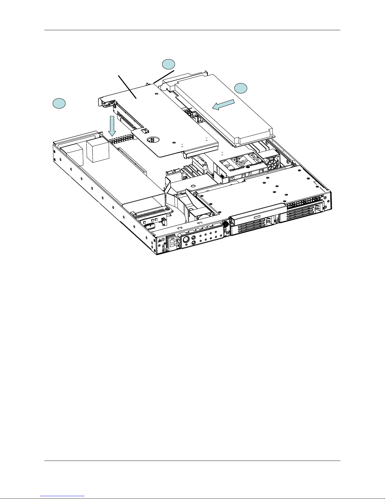
2.5.2 Full-Height, Full-Length PCI Adapter Subsystem
A one-slot PCI adapter assembly that supports one full-height/full-length PCI adapter is installed
in the PCI riser slot located at the left side of the SE7210TP1-E System Baseboard. This PCI
adapter assembly is configured and installed as shown in the following figure. After the PCI
adapter assembly is removed from the system, it is configured with one PCI adapter by plugging
the PCI adapter into the PCI connector on the riser card (either a 3.3 V riser card or a 5 V riser
card) that is part of the PCI adapter assembly. The PCI adapter assembly is then installed into
the system by plugging the riser card into the riser card connector on the SE7210TP1-E System
Baseboard. Finally, the thumb screw located on the back of the server is secured to the PCI
adapter assembly. Refer to the SE7210TP1-E System Baseboard specification for electrical
characteristics for this PCI adapter subsystem. The maximum power supported for PCI
adapters installed in the PCI Adapter subsystem is 25 watts.
Revision 1.0
16
Page 27
Intel® Carrier Grade Server TIGPT1U TPS System Overview
1-slot PCI Adapter Assembly - supports
one full-height/full-length PCI adapter or
one full-height/half-length PCI adapters
2
Install PCI Adapter
Assembly in System
Secure PCI Adapter Assembly to chassis
3
with captive fastener on back of chassis
Install PCI Adapter in
1
PCI Adapter Assembly
Figure 2-14. Full-Height, Full-Length PCI Adapter Subsystem
2.5.3 Power Subsystem
The Intel® Carrier Grade Server TIGPT1U can be configured with either a 250 watt AC-input
power supply or a 250 watt DC-input power supply.
The 250 watt power supply interconnects to the power interface board with a board-edge
connector. A board edge connector is also used by the extended front panel board to
interconnect to the power interface board. Power is then is carried to the 5 V riser board, the
midplane board, and the system baseboard via discrete cables connected to individual
connectors on the extended front panel board. The 250 watt power supply is capable of
handling the worst-case power requirements for a fully configured Intel
TIGPT1U. This includes one Intel
®
Pentium® 4 Processor, 4 GB of memory, two hard drives at
18 W per drive (typical worst case 3.5-inch by 1.0-inch, 15 k RPM drive), and one 25 watt PCI
adapter.
®
Carrier Grade Server
Revision 1.0
17
Page 28

System Overview Intel® Carrier Grade Server TIGPT1U TPS
2.5.4 Cooling Subsystem
2.5.4.1 Description
All system components except the power supply are cooled by two system fan assemblies.
One fan assembly is mounted near the middle of the chassis, and a second fan assembly is
mounted to the left of hard drive bay 1. These fan assemblies are shown in Figure 2-15.
Figure 2-15. System Fan Assemblies
One fan assembly contains two 40 x 48 mm counter rotating fans that are used to cool the Intel®
Pentium
®
4 Processor, and also contains one 40 x 28 mm fan that is used to cool the DDR
SDRAM memory and the processor Voltage Regulator Module (VRM) circuitry. Air to these
fans comes in the front of the chassis and passes over the SCSI disk drives helping to provide
cooling to the SCSI disk drives.
The other fan assembly contains one 40 x 28 mm fan that is used to cool the PCI adapter
(maximum of 25 watts) as well as the components on the SE7210TP1-E System Baseboard
that are located to the left of the Intel
®
Pentium® 4 Processor.
Each fan provides tachometer signal output to the SE7210TP1-E System Baseboard to indicate
a fan failure.
2.5.4.2 Ambient Temperature Control
The SE7210TP1-E System Baseboard contains a pulse-width-modulation (PWM) circuit, which
cycles the 12 Vdc fan voltage to provide quiet operation when system ambient temperature is
low and there are no fan failures. Under normal room ambient conditions (less than 24° C) the
fan power circuit supplies an effective fan voltage of 6.0 Vdc. When the room ambient
temperature exceeds 24° C, the fan control circuit provides increased voltage levels to increase
the speed of the fan. There are sixteen fan speed increments between 24° C and 40° C. At 40°
C the fans operate at their maximum speed to provide maximum airflow.
Revision 1.0
18
Page 29

Intel® Carrier Grade Server TIGPT1U TPS System Overview
2.5.4.3 Cooling Summary
The four-fan cooling subsystem is sized to provide cooling for:
• One Intel
®
Pentium® 4 Processor (3.0 GHz frequency, 1 M L2 cache, 800 MHz FSB,
90nm manufacturing technology)
• The SE7210TP1-E System Baseboard components
• 4 GB of SDRAM memory
• Two 15,000 RPM hard drives at a maximum of 18 watts per drive
• 1 PCI card at a maximum of 25 watts
The cooling subsystem is designed to meet acoustic and thermal requirements at the lower fan
speed settings. At the higher fan speed settings, thermal requirements are met for the
maximum ambient temperatures, but acoustic requirements are not met. The environmental
specifications are summarized in 2.7.1.
2.6 Server Management
The Telco SE7210TP1-E Server Baseboard server management architecture features the
National Semiconductor* PC87431M Baseboard Management Controller (mBMC), which
autonomously monitors server status and provides the interface to server management control
functions. This controller is responsible for controlling system power, resets, monitoring
voltages, temperatures, fans, and communicating with secondary controllers on its Intelligent
Platform Management Bus (IPMB).
The functions of the mBMC controller are summarized in the following section. The firmware for
the National Semiconductor* PC87431M* (mBMC) is not intended to be field upgraded. Refer
to the System Server Management External Architecture Specification for more details.
2.6.1 Baseboard Management Controller
The mBMC on the SE7210TP1-E System Baseboard provides server management monitoring
capabilities. A flash memory is associated with the mBMC that holds the operational code,
sensor data records (SDR), and system event log (SEL). There is also a serial Electrical
Erasable Programmable Read Only Memory (EEPROM) that holds the mBMC configuration
defaults and field replaceable unit (FRU) information. The various server management
functions provided by the Bus Management Controller (BMC) are listed as follows:
• Baseboard voltage monitoring
• Fan failure detection
• Fan speed control
• Processor voltage monitoring
• Processor presence detection
• Processor internal error (IERR) monitoring
• Fault resilient booting (FRB)
• Watchdog timer
• Periodic system management interrupt (SMI) timer
• One I
• System event log (SEL) management and access
2
C management bus interface for communicating with SIO and ADT7463
Revision 1.0
19
Page 30

System Overview Intel® Carrier Grade Server TIGPT1U TPS
• Sensor data record (SDR) repository management and access
• Processor nonmaskable interrupt (NMI) monitoring
• Processor System Management Interrupt (SMI) monitoring
• Time-stamp clock
• Secure mode and video blank
• Software front panel NMI generation
2.7 Specifications
2.7.1 Environmental Specifications
The Intel® TIGPT1U has been tested to the environmental specifications as indicated in Table
2-4. All testing was performed per procedures defined in Bellcore GR-63-CORE NEBS Physical
Protection, Bellcore GR-3580 NEBS Criteria Levels, Bellcore GR-1089-CORE EMC and
Electrical Safety – Generic Criteria for Network Telecommunications Equipment, and the Intel
Environmental Standards Handbook.
Table 2-4. Environmental Specifications Summary
Environment Specification
Temperature operating 5o C to 40o C (41o F to 104o F)
Temperature nonoperating -40o C to 70o C (-104o F to 158o F)
Altitude 0 to 1,800 m (0 to 5,905 ft)
Humidity nonoperating 95%, noncondensing at temperatures of 23o C (73o F) to 40o C (104o F)
Vibration operating Swept sine survey at an acceleration amplitude of 0.1 g from 5 to 100 Hz and
back to 5 Hz at a rate of 0.1 octave/minute, 90 minutes per axis on all three
axes as per Bellcore GR-63-CORE standards
Vibration nonoperating Swept sine survey at an acceleration amplitude of 0.5 g from 5 to 50 Hz at a
rate of 0.1 octaves/minute, and an acceleration amplitude of 3.0 g from 50 to
500 Hz at a rate of 0.25 octaves/minute, on all three axes as per Bellcore GR63-CORE standard.
2.2 Grms, 10 minutes per axis on all three axes as per the Intel
Environmental Standards Handbook
Shock operating Half-sine 2 G, 11 ms pulse, 100 pulses in each direction, on each of the three
axes as per the Intel
Shock nonoperating Trapezoidal, 25 G, 170 inches/sec delta V, three drops in each direction, on
each of the three axes as per Intel
Safety UL 1950, CSA 950, IEC 950, TUV/GS EN60950
Emissions Certified to FCC Class A; tested to CISPR 22 Class A,
EN 55022 Class A, VCCI Class A ITE, AS/NZS 3548 Class A
Immunity Verified to comply with EN 50082-1
Electrostatic discharge (ESD) Tested to ESD levels up to 15 kilovolts (kV) air discharge and up to 8 kV
contact discharge without physical damage as per Intel
Standards Handbook
Acoustic
Sound pressure: < 55 dBA at ambient temperatures < 24° C measured at
bystander positions in operating mode
®
Environmental Standards Handbook
®
Environmental Standards Handbook
®
®
Environmental
®
Revision 1.0
20
Page 31

Intel® Carrier Grade Server TIGPT1U TPS System Overview
2.7.2 Physical Specifications
Table 2-5 describes the physical specifications of the Intel® TIGPT1U.
Table 2-5. Dimensions and Weight
Height 1.70 inches (43 mm)
Width 16.9 inches (430 mm)
Depth 20 inches (509 mm)
Front clearance 2 inches (76 mm)
Side clearance 1 inches (25 mm)
Rear clearance 3.6 inches (92 mm)
Revision 1.0
21
Page 32

Cables and Connectors Intel® Carrier Grade Server TIGPT1U TPS
3. Cables and Connectors
This chapter describes interconnections between the various components of the Intel® Carrier
Grade Server TIGPT1U. In addition, this chapter includes an overview diagram of the Intel
®
TIGPT1U interconnections, as well as tables describing the signals and pin-outs for the
connectors on the various system boards. Refer to the appropriate SE7210TP1-E System
Baseboard section or system board sections in this document for other connector signal
descriptions and pin-outs.
3.1 Chapter Structure and Outline
The information contained in this chapter is organized into four sections. The information is
presented in a modular format, with numbered headings for each major topic and subtopic. The
content of each section is summarized as follows:
Section 3.2: Interconnect Block Diagram
Provides an overview of system interconnects.
Section 3.3: Cable and Interconnect Descriptions
Provides a list of all the connectors and cables in the system.
Section 3.4: User-accessible Interconnects
Describes the form-factor and pin-out of user-accessible interconnects.
Revision 1.0
22
Page 33

Intel® Carrier Grade Server TIGPT1U TPS Cables and Connectors
3.2 Interconnect Block Diagram
Figure 3-1 shows interconnections for all of the boards used in the Intel® TIGPT1U.
System Baseboard
Serial
Alarm Conn
2x5 COM
Fan 4
2x5
2 NIC, 2 USB, COM2, 1 Kybd/
2x8 Alarm
Fan 3
1x3
1x3
1x3 Fan
Mouse, 1 Video
1x3 Fan
Pwr
2x4
2x4 uP Pwr
250 W Power Supply
(AC-input or DC-input)
Power Conn 2x31
Power Conn 2x31
Interconnect Board
Power Conn 2x31
Power Conn 2x31
3.3V to 5V Regulator 5A
Pwr 2x6
2x6 MP PWR
Extended Front
Panel Board
USB 2x5
Push Buttons
C
U
Pwr|Rst
O
S
M
B
2
NMI|ID
2x5 Pin USB Cbl
System Fault LEDs
Crt|Mjr|Mnr|Pwr
Activity/ID LEDs
ID|NIC|On|Disk1|Disk0
1x3 pwr cbl (5V)
1x3 pwr
cbl (5V)
1x3 Fan
Pwr 1x3
Fan 5
1x3
Fan 6
1x3
68 Pin Wide U-320
SCSI CBL
2x5 Pin USB Cbl
2x17 Front
Panel Cable
uP
2x4
2x6 MP PWR
1x3 Fan
FP 2x17
FP 2x17
2x4 uP Pwr
1x3 Fan
Fan 6
40x28
6300ESB
I/O Controller
Hub
2x20 IDE
Cable
Pwr 2x6
SCSI SCA Conn 80pin SCSI SCA Conn 80pin
SCSI SCA Conn 80pin
SCSI Hard Drive 1
Hot Plug Drive Assembly
Consists of:
1. SCA SCSI Disk Drive
2. Drive Carrier
SCSI Hard Drive Bay 1 SCSI Hard Drive Bay 0
2x20 IDE Cable
CDROM
Signal 2x20, Power 1x2
CDROM
MidPlane Board
SCSI LVD Term
1x2 CDROM Pwr
1/2"
Pentium 4
uPGA478
827210
Memory
Controller
Fan 1
1x3
1x3 Fan
Fan 1/3
40x48
SCSI SCA Conn 80pin
SCSI Hard Drive 0
Hot Plug Drive Assembly
Consists of:
1. SCA SCSI Disk Drive
2. Drive Carrier
CDROM Drive Bay
Note: The CDROM
Drive is positioned
above SCSI Hard
Drive Bay 1
Hub
Fan 2
1x3
1x3 Fan
Fan 2/4
40x48
68 Pin Wide U-320
SCSI CBL
SCSI BB Conn
68 Pin Wide U-320 SCSI Bus
Fan 5
40x28
Figure 3-1. Intel® Carrier Grade Server TIGPT1U Interconnect Block Diagram
Revision 1.0
23
Page 34

Cables and Connectors Intel® Carrier Grade Server TIGPT1U TPS
3.3 Cable and Interconnect Descriptions
Table 3-1 describes all cables and connectors of the Intel® Carrier Grade Server TIGPT1U.
Table 3-1. System Interconnect Descriptions
System
Board
Baseboard J5G2 1 x 5 P/S Signal Connector P/S Sig Cable J5G2 1 x 5 P/S Signal
Baseboard J4J1 2 x 12 P/S Power
Baseboard J9B1 2 x 4 uP Power Connector P/S uP Pwr Cbl J9B1 2 x 4 uP Power Connector
Baseboard J4J2 2 x 20 IDE Connector IDE Cable J4J2 2 x 20 IDE Connector
Baseboard J1J1 68 pin SCSI Ch B Conn SCSI BB Cbl J1J1 68 pin SCSI Connector
Baseboard J8A2 2 x 5 Serial Port Connector USB/Com2/Alrm J8A2 2 x 5 Serial Port
Baseboard J5A1 1 x 3 Fan 1 Pwr/Tach Conn 40 x 48 Fan
Baseboard J7A2 1 x 3 Fan 2 Pwr/Tach Conn 40 x 48 Fan Left J7A2 1 x 3 Fan Pwr/Tach Conn
Baseboard J7J3 1 x 3 Fan 3 Pwr/Tach Conn 40 x 48 Fan
Baseboard J7J2 1 x 3 Fan 4 Pwr/Tach Conn 40 x 48 Fan Left J7J2 1 x 3 Fan Pwr/Tach Conn
Baseboard J1E2 1 x 3 Fan 5 Pwr/Tach Conn 40 x 28 Fan PCI J1E2 1 x 3 Fan Pwr/Tach Conn
Baseboard J1E1 1 x 3 Fan 5 Pwr/Tach Conn 40 x 28 Fan
Baseboard J3J2 2 x 17 Front Panel Conn Front Panel (FP)
Baseboard J5G1 2 x 5 USB Connector USB Cable J5G1 2 x 5 USB Connector
MP Board J2L1 68 pin SCSI Connector SCSI BB Cbl J2L1 68 pin SCSI Connector
MP Board J4A1 80 pin SCA Connector SCSI Drive 1 J4A1 80 pin SCA Connector
MP Board J8A1 80 pin SCA Connector SCSI Drive 2 J8A1 80 pin SCA Connector
MP Board J9L1 2 x 6 MP-FP Connector MP-FP Cable J9L1 2 x 6 MP-FP Connector
FP Board J1E1 2 x 6 MP Power Conn MP-FP Cable J1E1 2 x 6 MP-FP Connector
FP Board J3H1 1 x 3 Riser Power Conn P/S CDRsr Cb J3H1 1 x 3 Riser Power Conn
FP Board J2G1 1 x 8 USB Connector USB Cable J2G1 1 x 8 USB Connector
FP Board J5A1 2 x 4 uP Power Connector P/S uP Pwr Cbl J5A1 2 x 4 uP Power Connector
FP Board J8A1 2 x 17 Front Panel Conn FP Cable J8A1 2 x 17 Front Panel Conn
FP Board J9B1 2 x 12 COM2/Alarm Conn C2/Alarm Cbl J9B1 2 x 12 COM2/Alarm Conn
FP Board J9A1 2 x 5 PS Sig/Pwr Conn PS Sig/Pwr Cbl J9A1 2 x 5 PS Sig/Pwr Conn
FP Board J10A1 2 x 10 PS Pwr Conn PS Pwr Cable J10A1 2 x 10 PS Pwr Conn
FP Board J1J1 RJ45 COM2/ USB con N/C
Ref
Des
Connector Description Cable/Device
/Board
SE7210TP1-E Baseboard Connections
P/S Pwr Cable J4J1 2 x 12 P/S Power Conn
Connector
Right
Right
Mem
Cable
Midplane Board Connections
Extended Front Panel Board
Ref
Des
J5A1 1 x 3 Fan Pwr/Tach Conn
J7J3 1 x 3 Fan Pwr/Tach Conn
J1E1 1 x 3 Fan Pwr/Tach Conn
J3J2 2 x 17 Front Panel Conn
Connector Description
Connector
Connector
Revision 1.0
24
Page 35

Intel® Carrier Grade Server TIGPT1U TPS Cables and Connectors
CDROM Interface Board Connections
CDROM I/F P1 2 x 1 Power Connector CDROM Pwr Cb P1 2 x 1 Power Connector
CDROM I/F P3 2 x 20 IDE Connector IDE Cable P3 2 x 20 IDE Connector
NEBS Riser Board Connections
NEBS Rsr J1A1 1 x 3 Power Connector P/S CDRsr Cb J1A1 1 x 3 Power Connector
3.4 Exteranly-Accessible Interconnects
3.4.1 Keyboard and Mouse Ports
PS/2 keyboard and mouse connectors are located on the back panel. The +5 V lines to these
connectors are protected with a PolySwitch* circuit that, like a self-healing fuse, reestablishes
the connection after an overcurrent condition is removed.
NOTE
✏
The keyboard is supported in the bottom PS/2 connector and the mouse is supported in the top
PS/2 connector. Power to the server should be turned off before a keyboard or mouse is
connected or disconnected.
The keyboard controller contains the AMI keyboard and mouse controller code, provides the
keyboard and mouse control functions, and supports password protection for power-on/reset. A
power-on/reset password can be specified in the BIOS Setup program.
Table 3-2. Keyboard/Mouse PS/2 Connector Pin Out (J9A1)
Connector Pin Signal Name
Keyboard
Mouse
1 Data
2 NC
3 GND
4 +5 V (Fused)
5 Clock
6 NC
7 Data
8 NC
9 GND
10 +5 V (Fused)
11 Clock
12 NC
13 NC
14 NC
15 NC
16 NC
17 NC
Revision 1.0
25
Page 36

Cables and Connectors Intel® Carrier Grade Server TIGPT1U TPS
3.4.2 Serial Ports
The Intel® Server Board SE7210TP1-E has one 9-pin D-sub serial port connector for COM1 and
one 2 x 5 serial port connector COM2. COM2 is brought out the front of the chassis by an RJ45
connector. by cabling between the 2 x 5 serial port connector on the Intel
SE7210TP1-E and a mating connector on the extended front panel board. The following tables
detail the pin outs of these two ports.
Table 3-3. COM1: 9-pin Serial A Port Pin Out (J8A1)
Pin Signal
1 DCD (Data Carrier Detect)
2 RXD (Receive Data)
3 TXD (Transmit Data)
4 DTR (Data Terminal Ready)
5 GND
6 DSR (Data Set Ready)
7 RTS (Request to Send)
8 CTS (Clear to Send)
9 RI (Ring Indicator)
The front panel board has provision for the COM2 port using a RJ45 connector. This
RJ45 connector is accessible at the front of the system.
®
Server Board
Table 3-4. COM2: Serial Port Connector on Front Panel
Pin Signal
1 RTS (request to send)
2 DTR (data terminal ready)
3 TXD (transmit data)
4 GND
5 RIA (ring indicator)
6 RXD (receive data)
7 DSR/DCD (date set ready / data carrier detect1)
8 CTS (clear to send)
1
Use jumper on extended front panel board to select
Revision 1.0
26
Page 37

Intel® Carrier Grade Server TIGPT1U TPS Cables and Connectors
3.4.3 Video Port
The video port interface is a standard VGA compatible, 15-pin connector. Onboard video is
supplied by an ATI* Rage* XL video controller with 8 MB of onboard video SGRAM.
Table 3-5. Video Connector
Pin Signal
1 Red (analog color signal R)
2 Green (analog color signal G)
3 Blue (analog color signal B)
4 No connection
5 GND
6 GND
7 GND
8 GND
9 Fused VCC (+5 V)
10 GND
11 No connection
12 V_MONID1
13 HSYNC (horizontal sync)
14 VSYNC (vertical sync)
15 V_MONID2
3.4.4 Universal Serial Bus (USB) Interface
The baseboard provides four USB ports. USB ports 1, 2, and 3 are brought out the rear of the
unit on the baseboard, and USB port 4 is brought out the front of the unit on the extended front
panel. The front USB port is accessible without removing the front bezel. The built-in USB ports
permit the direct connection of four USB peripherals without an external hub. If more devices
are required, an external hub can be connected to any of the built-in ports.
Table 3-6. Single USB Connector
Pin Signal
1 Fused VCC (+5 V w/over-current monitor of ports 0, 1, 2, and 3)
2 DATAL0 (differential data line paired with DATAH0)
3 DATAH0 (differential data line paired with DATAL0)
4 GND
5 GND
6 GND
Revision 1.0
27
Page 38

Cables and Connectors Intel® Carrier Grade Server TIGPT1U TPS
3.4.5 Ethernet Connector
The server board SE7210TP1-E supports two NIC RJ45 connectors for the Ethernet ports. The
following table details the pin-out of each of the connectors.
Table 3-7. Magjack Connector (RJ45, 10/100/1000) Pin Out (J5A1, J6A2)
Pin Signal Name Pin Signal Name
1 LAN_V_1P8 10 LAN_MDI_0*
2 LAN_MDI_2* 11 LAN_MDI_0
3 LAN_MDI_2 12 LAN_V_1P8
4 LAN_MDI_1 13 LAN_LINK_100*
5 LAN_MDI_1* 14 LAN_LINK
6 LAN_V_1P8 15 LAN_LINK_UP*
7 LAN_V_1P8 16 LAN_ACTLED*
8 LAN_MDI_3 17 GND
9 LAN_MDI_3* 18 GND
3.4.6 Telco Alarms Connector
The system provides one telco DB15 alarms connector on the rear bulkhead. Table 3-8 shows
the pinout for the telco alarms connector, and Figure 3-2 shows the telco alarms connector as
viewed from the back of the server.
Table 3-8. Telco Alarms Connector
Pin Description Pin Description
1 MinorReset + 9 MinorAlarm – NC
2 MinorReset - 10 MinorAlarm - COM
3 MajorReset + 11 MajorAlarm - NO
4 MajorReset - 12 MajorAlarm - NC
5 CriticalAlarm - NO 13 MajorAlarm - COM
6 CriticalAlarm - NC 14 PwrAlarm - NO
7 CriticalAlarm - COM 15 PwrAlarm - COM
8 MinorAlarm - NO
18
915
3.4.7 AC Power Input for AC-Input Power Supply
One IEC320-C13 receptacle is provided at the rear of the AC-input power supply. It is
recommended to use an appropriately sized power cord and AC main. Please refer to Section
9, AC Power Subsystem, in this document for system voltage, frequency, and current draw
specifications.
Revision 1.0
28
Figure 3-2. Telco Alarms Connector
Page 39

Intel® Carrier Grade Server TIGPT1U TPS Cables and Connectors
Figure 3-3. AC Power Input Connector
3.4.8 DC Power Input for DC-Input Power Supply
A DC power terminal block is provided at the rear of the DC-input power supply. It is
recommended to use appropriately sized power wire and DC main.
Figure 3-4. DC Power Input Connector
The terminal block will accept standard terminal lugs size Newark stock # 81N1501 type CRST0-1406-HT that accept 14 AWG wire gauge. The width (w, see Figure 2-1) of the lug can be
no larger than 0.25 inches.
Figure 3-5. Terminal Lug
Revision 1.0
29
Page 40

Extended Front Panel System Board Intel® Carrier Grade Server TIGPT1U TPS
4. Extended Front Panel System Board
This chapter describes the basic functions and interface requirements of the Extended Front
Panel system board that is designed for the Intel
®
Carrier Grade Server TIGPT1U.
4.1 Features
• Four switches to control power-on, reset, NMI, and the system ID LED
• One system ID LED that can be controlled remotely or by the system ID switch
• Two system activity LEDs that indicate power-on and NIC activity
• Two hard drive activity/fault LEDS that indicate activity/fault status for drives 0 and 1
• Four system fault LEDs that indicate critical, major, minor, and power system fault status
• Four system fault relays for external critical, major, minor, and power fault indicators
• Hot-swap circuitry for controlling power delivery to SCSI disk drives 0 and 1
• Power distribution to SE7210TP1-E System Baseboard, drive carrier assemblies, and
hot plug disk drives 1 and 2
4.2 Chapter Structure and Outline
The information contained in this chapter is organized into eight sections. The information is
presented in a modular format, with numbered headings for each major topic and subtopic. The
content of each section is summarized as follows:
Section 4.3: Introduction
Provides an overview of the Intel
showing primary components and their relationships, and physical board
layout diagrams.
®
TIGPT1U extended front panel board,
Section 4.4: Functional Description of Front Panel Switches, LEDs, and Relays
Provides a functional description of the front panel switches, LEDs, and
relays contained on the FPIO board.
Section 4.5: Connector Information
Provides information on all connectors contained on the extended front
panel board. Gives signal descriptions and the corresponding electrical
parameters for each input and output of a given connector.
Section 4.6: SCSI Power Subsystem
Provides information on the hard drive interface circuitry on the extended
front panel board. The hard drive interface circuitry is designed to give
the end user support for two SCSI hot-plug hard drives. The design
enables easy use and replacement of the SCSI hard drives without
powering down the system.
Section 4.7: Specifications
Describes the electrical, environmental and mechanical specifications.
Revision 1.0
30
Page 41

Intel® Carrier Grade Server TIGPT1U TPS Extended Front Panel System Board
4.3 Introduction
The extended front panel system board provides the means of mounting and electrically
connecting switches and indicators for system operation and status. These features are
accessible and visible from the front of the chassis. In addition, it contains the hard drive hotplug control circuitry necessary for the hot-plug SCSI disk drives. An alarms function is also
provided. The extended front panel system board is designed for use with telecom
SE7210TP1-E Server Baseboards.
Power
34 Pin Front Panel
Connector
Supply
Aux I
BUS
2
C
MidPlane
Connector
Alarm/COM2
Connector
USB
Connector
PCF 8574
Front Panel
LEDs
Hot Swap
Power
Cntrl
12V & 5V
Front Panel
COM2/USB
Connector
Front Panel
Switches
C BUS
2
I
PCF 8574
Alarms
Circuits
Figure 4-1. Extended Front Panel Board
4.4 Functional Description of Front Panel Switches, LEDs, and
Relays
4.4.1 Front Panel Switches
The front panel has a power switch, a reset switch, an NMI switch, and a system ID switch. The
function of each switch is described in the following table.
Switch Function
Power Switch A momentary switch, APCI compliant, used to toggle system power on/off.
Reset Switch A momentary switch used to reset the system when it is in the power-on
state.
NMI Switch A momentary switch used to instruct the processor to copy system memory
to hard disk
System ID Switch A momentary switch used to instruct the processor to toggle the state of the
system ID LED
Revision 1.0
Table 4-1. Front Panel Switch Description
31
Page 42

Extended Front Panel System Board Intel® Carrier Grade Server TIGPT1U TPS
4.4.2 Front Panel LEDs
Table 4-2. LED Specifications
LED Function LED Color Peak Wavelength
(nm)
ID White N/A 50 36
Blue 470 50 18
NIC Green 560 12 6
ON Green 560 12 6
DRV 1/0 Activity Green 568 12 2.6
DRV 1/0 Red 625 12 4.0
CRT Red 660 23 6
Yellow-Green 570 16.8 6
MJR Red 660 23 6
Yellow-Green 570 16.8 6
MNR Yellow 580 5.9 3
PWR Yellow 580 5.9 3
Luminous
Intensity
Typ(mcd)
Luminous
Intensity
Min(mcd)
4.4.3 System Status LEDs
There are five extended front panel system board system status LEDs. The function of these
system status LEDs is described in the following table.
Table 4-3. Front Panel System Status LED Description
Status LED Function
Power The green Power LED indicates that system power is on when it is
illuminated continuously. When it is blinking green, it indicates that the
system is in ACPI sleep mode.
NIC0/NIC1 The green NIC activity LED indicates network link presence and activity on
either NIC0 or NIC1
System ID The white or blue NIC activity LED is used to identify a particular system.
The LED can be toggled remotely or with the System ID Switch
Disk 0 The green/amber/red hard drive 1 activity/fault LED displays activity or fault
status for hard disk drive 1
Disk 1 The green/amber/red hard drive 2 activity/fault LED displays activity or fault
status for hard disk drive 2
Revision 1.0
32
Page 43

Intel® Carrier Grade Server TIGPT1U TPS Extended Front Panel System Board
4.4.4 System Fault LEDs
There are four front panel system fault LEDs. The function of these system fault LEDs is
described in the following table.
Table 4-4. Front Panel System Fault LED Description
Fault LED Function
Critical This amber or red LED alarm is illuminated via the Server Management Bus
(SMBus) and may only be turned off via SMBUS control. When continuously
lit, it indicates the presence of a Critical System Fault. A critical system fault
is an error or event that is detected by the system with a fatal impact to the
system. In this case, the system cannot continue to operate. An example
could be the loss of a large section of memory, or other corruption, that
renders the system not operational. The front panel critical alarm relay will
be engaged.
Major This amber or red major alarm is illuminated via SMBUS bus and may be
turned off via SMBUS control or alarm connector reset. When continuously
lit, it indicates the presence of a Major System Fault. A major system fault is
an error or event that is detected by the system that has discernable impact
to system operation. In this case, the system can continue to operate, but in
a “degraded” fashion (reduced performance or loss of non-fatal feature
reduction). An example could be the loss of one of two mirrored disks. The
front panel major alarm relay will be engaged.
Minor This amber LED minor alarm is illuminated via SMBUS bus and may be
turned off via SMBUS control or alarm connector reset. When continuously
lit, it indicates the presence of a Minor System Fault. A minor system fault is
an error or event that is detected by the system but has little impact to actual
system operation. An example would be a correctable ECC error. The front
panel minor alarm relay will be engaged.
Power The amber power alarm is illuminated via SMBUS bus or SYS_FLT_LED_L
signal and may only be turned off via SMBUS control. When continuously lit,
it indicates the presence of a Power System Fault. The front panel power
alarm relay will be engaged.
4.4.5 LED Color Selection
The Extended Front Panel Board (XFPB) supports population options for two different SKUs,
the Intel
fault LEDs. The OEM SKU supports a blue ID LED and red hard disk drive (HDD) fault LEDs.
Selecting between the two SKUs are done during board build. For an Intel
LED at location DS4J2 and install n-FETs at locations Q5W6 and Q5W2. For an OEM SKU,
install a blue LED at location DS4J2 and remove n-FETs at locations Q5W6 and Q5W2. LED
color selection to support the Intel
Revision 1.0
®
SKU and an OEM SKU. The Intel® SKU supports a white ID LED and amber HDD
®
SKU, install a white
®
SKU and OEM SKU are outlined in the following table:
Table 4-5. LED Color Selection
Board
SKU
OEM ID Blue DS4J2 Install iPN 697565-010
Intel ID White DS4J2 Install iPN 697565-009
OEM Disk 0 Fault Red Q5W6 Remove component
Intel Disk 0 Fault Amber Q5W6 Install component
OEM Disk 1 Fault Red Q5W2 Remove component
Intel Disk 1 Fault Amber Q5W2 Install component
LED Color Board Location Reference
Designator
Board Population Option
33
Page 44

Extended Front Panel System Board Intel® Carrier Grade Server TIGPT1U TPS
4.4.6 System Fault Relays
The front panel board contains four relays. These relays are for power, critical, major and minor
alarms. The relays are controlled via the SMBus. See Section 4.4.7 for programming
information.
4.4.7 Server Management Bus (SMBus) Interface
The Torrey Pines baseboard communicates to the XFPB via the auxiliary I2C bus to support
server management functions. The I
SMBus functionality. Two I/O expanders on the XFPB are used as slave devices to interface to
the SMBus.
The first device (U3H1) is used to support the control and monitoring of the front panel alarms.
All signals at U3H1 that interface to the alarms circuitry are active low. During power up, the
device will reset all I/Os to the default High state. However, during system soft resets, the
device requires a software command to reinitialize all I/Os to the default inactive state.
Access to U3H1 during a write cycle can be performed by writing to address 0 x 40. Access to
U3H1 during a read cycle can be performed by writing to address 0 x 41. Refer to Table 4-6 for
an I/O map of U3H1.
2
C interface operates at less than 20 Khz rate to support
The second device (U2H1) is used to support the control and monitoring of the two SCSI hard
drives. Also, during a drive fault condition, U2H1 receives commands from the baseboard to
activate the proper drive fault LED to provide visual indications of a fault condition. All signals at
U2H1 that interface to the SCSI control circuitry are active low. During power up, the device will
reset all I/Os to the default High state. However, during system soft resets, the device requires
a software command to reinitialize all I/Os to the default inactive state.
Access to U2H1 during a write cycle can be performed by writing to address 0 x 44. Access to
U2H1 during a read cycle can be performed by writing to address 0 x 45. Refer to Table 4-7 for
an I/O map of U2H1.
Table 4-6. Alarms SMBus I/O Mapping
Bit I/O Name Description
0 O Power alarm Writing 0 turns on the power alarm relay and illuminates the POWER LED,
writing 1 turns both off. The relay and LED may also be turned on by a
FAN_FAIL_L signal.
1 O Critical alarm Writing 0 turns on the critical alarm relay and illuminates the CRITICAL LED,
writing 1 turns both off.
2 O Major alarm Writing a 1 to 0 edge will turn on the flip-flip that enables major alarm relay.
Writing a 1 will turn off the major alarm relay or a MAJOR_RESET signal input.
MAJOR LED in on when output is 0, off when output is 1. 1
3 O Minor alarm Writing a 1 to 0 edge will turn on the flip-flip that enables major alarm relay.
4 I Major alarm
sense
5 I Minor alarm
sense
Writing a 1 will turn off the major alarm relay or a MINOR_RESET signal input.
MINOR LED in on when output is 0, off when output is 1.
Senses the state of the major alarm relay. 0 relay is on, 1 relay is off. This
allows software to detect if the MAJOR_RESET signal was activated. Always
write 1 during write operations.
Senses the state of the minor alarm relay. 0 relay is on, 1 relay is off. This
allows software to detect if the MINOR_RESET signal was activated. Always
write 1 during write operations.
1
Revision 1.0
34
Page 45

Intel® Carrier Grade Server TIGPT1U TPS Extended Front Panel System Board
Bit I/O Name Description
6 I Critical/Major
color
7 I Not used Reserved for future use, always write 1 during write operations.
1
Normally closed (NC) and normally open (NO) relay contacts are provided on the rear panel Telco alarms
connector. To activate the relay, a 1 to 0 transition must be written.
Writing a 1 turns CRITICAL and MAJOR LEDs to yellow, writing 0 color is
RED. Strapping J7D1 pins 7-8 forces LEDs to RED. Resets to yellow.
Table 4-7. SCSI SMBus I/O Mapping
Bit I/O Name Description
0 O SCSI1_LED_FLT_N Writing 0 to this signal will activate the SCSI drive fault circuitry and
illuminate the SCSI1 fault LED.
1 O SCSI0_LED_FLT_N Writing 0 to this signal will activate the SCSI drive fault circuitry and
illuminate the SCSI0 fault LED.
2 O SCSI1_INSERTED_N This signal provides a future use option to allow server management to
control activation of the SCSI1 drive power delivery circuitry. Writing 0 to
this signal will enable the hot swap circuitry to power on. However, the
signal is set to the disabled mode in the current board configuration.
3 O SCSI0_INSERTED_N This signal provides a future use option to allow server management to
control activation of the SCSI1 drive power delivery circuitry. Writing 0 to
this signal will enable the hot swap circuitry to power on. However, the
signal is set to the disabled mode in the current board configuration.
4 I SCSI1_MATED_N This signal senses drive presence at SCSI drive slot 1. A low state at this
signal indicates that a drive is populated at slot 1
5 I SCSI0_MATED_N This signal senses drive presence at SCSI drive slot 0. A low state at this
signal indicates that a drive is populated at slot 0
6 I SCSI_PWRGOOD1 This signal senses the state of the SCSI drive 1 hot swap controller. A low
state at this signal indicates that no power is delivered to drive 1.
7 I SCSI_PWRGOOD0 This signal senses the state of the SCSI drive 1 hot swap controller. A low
state at this signal indicates that no power is delivered to drive 1.
4.5 Connector Information
The following tables show all the connectors on the XFPB and the interconnection to other
devices within the Intel
following figure of the connector location.
Table 4-8. Extended Front Panel System Board Connector Information
Loc Ref Des Function Interconnect Connects to
1 J2G1 1 x 8 USB Connector USB Cable Baseboard USB Connector
2 J5A1 2 x 4 Processor Power Conn uP Pwr Cable Baseboard uP Power Connector
3 J8A1 2 x 17 Front Panel Conn FP Cable Baseboard Front Panel Connector
10 J1E1 2 x 6 Midplane Pwr/Sig
11 J9A1 2 x 5 Power Conn Pwr/Sig Cable Baseboard Power/Signal Connector
12 J9B1 2 x 12 Alarm/COM2 Conn Alarm/Com Cbl Baseboard COM2/Chassis Alarm
13 J10A1 2 x 10 Power Connector Power Cable Baseboard Power Connector
14 J1J1 RJ45 COM2/USB Conn N/C
16 J3H1 1 x 3 NEBS Riser Pwr Conn Riser Pwr Cbl NEBS Riser Power Connector
Revision 1.0
®
TIGPT1U. In addition, the first column references the location on the
FPIO Board Connections
MP Cable Midplane Power/Signal Connector
35
Page 46

Extended Front Panel System Board Intel® Carrier Grade Server TIGPT1U TPS
Figure 4-2. Extended Front Panel Board Connector Location
Table 4-9. Connector Housing Information
Conn Function Intel PN AML s/k/l/p* cnt hsn
J2G1 USB 1 x 8 C13083-007 Molex 43650-0817 y/y/y/y 30u” 94V0
J5A1 uP Pwr 2 x 4 A81170-001 Molex 39-29-9086 y/y/y/y Tin 94V0
J8A1 FP 2 x 17 A57940-002 Foxconn HL15177 y/y/y/y 15u” 94V0
J1E1 MP 2 x 6 691314-004 Molex 43045-1218 y/y/y/y Tin 94V0
J9A1 BB Pwr/Sig 2 x 5 2
mm
J9B1 Alarm/COM 2 x 12 2 mm A62345-003 Molex 87333-2420 y/y/n/y 15u” 94V0
J10A1 Baseboard (BB) Pwr
2 x 10
J1J1 COM2/USB 680356-004 680358-004 y/y/y/y 30u” 94V0
J3E1 Riser Pwr 1 x 3 703140-002 Molex 39-30-2036 y/y/y/y Tin 35u” 94V0
s/k/l/p* - shrouded/keyed/latching/polarized
Extended Front Panel Board
700000-772 Molex 87333-1021 y/y/n/y 30u” 94V0
703141-001 Molex 39-29-9207 y/y/y/y Tin 35u” 94V0
Revision 1.0
36
Page 47

Intel® Carrier Grade Server TIGPT1U TPS Extended Front Panel System Board
4.5.1 Extended Front Panel Board USB Connector Pinout
The following table details the pin-out of the USB connector to the SE7210TP1-E System
Baseboard.
Table 4-10. 8-pin (1 x 8) USB J2G1 Connector
Pin USB Signal
1 GND
2 GND
3 FP_USB_N
4 FP_USB_P
5 USBPWR
6 GND
7 GND
8 GND
4.5.2 Extended Front Panel Board uProcessor Power Connector Pinout
The following table details the pin-out of the uP power connector to the SE7210TP1-E System
Baseboard.
Table 4-11. 8-pin (2 x 4) uP Power J5A1 Connector
Pin uP Power Signal Pin uP Power Signal
1 GND 2 P12V_A
3 GND 4 P12V_A
5 GND 6 P12V_A
7 GND 8 P12V_A
Revision 1.0
37
Page 48

Extended Front Panel System Board Intel® Carrier Grade Server TIGPT1U TPS
4.5.3 Extended Front Panel Board Front Panel Connector Pinout
The following table details the pin-out of the front panel connector to the SE7210TP1-E System
Baseboard.
Table 4-12. 34-pin (2 x 17) Front Panel J8A1 Connector
Pin Front Panel Signal Pin Front Panel Signal
1 GND 2 P5V_STBY
3 Keying Pin 4 NC_FAN_FAIL_PWR
5 PWR_ON_LED_N 6 NC_POWER_FAIL_PWR
7 NC_HD_ACT_PWR 8 NC_POWER_FAIL_PWR
9 NC_HD_ACT_N 10 FP_SYS_FLT_LED_N
11 FP_PWR_BTN_N 12 P3V3_STBY
13 GND 14 NIC1_LED_N
15 FP_RST_BTN_N 16 NC_FP_SDA
17 GND 18 NC_FP_SCL
19 NC_SLEEP_BTN 20 NC_SSI_PIN20
21 GND 22 P3V3_STBY
23 FP_NMI_BTN_N 24 NIC2_LED_N
25 NC_SSI_PIN25 26 NC_SSI_PIN26
27 P5V_STBY 28 P5V_STBY
29 FP_ID_LED_N 30 STATUS_LED_N
31 FP_ID_LED_N 32 P5V
33 GND 34 NC_HDD_FLT_N
4.5.4 Extended Front Panel Board Midplane Connector Pinout
The following table details the pin-out of the connector to the Mid-Plane System Baseboard.
Table 4-13. 12-pin (2 x 6) Mid-Plane J1E1 Connector
Pin Mid-Plane Signal Pin Mid-Plane Signal
1 SCSI0_5V 2 SCSI0_12V
3 SCSI1_5V 4 SCSI1_12V
5 ACT_SCSI0_N 6 P5V
7 GND 8 GND
9 GND 10 SCSI0_MATED_N
11 ACT_SCSI1_N 12 SCSI1_MATED_N
Revision 1.0
38
Page 49

Intel® Carrier Grade Server TIGPT1U TPS Extended Front Panel System Board
4.5.5 Extended Front Panel Board Power/Signal Connector Pinout
The following table details the pin-out of the power/signal connector to the SE7210TP1-E
System Baseboard.
Table 4-14. 10-pin (2 x 5) Power/Signal J9A1 Connector
Pin Power/Signal Signal Pin Power/Signal Signal
1 PS_SCL 2 PS_SDA
3 PS_ALERT_N 4 GND_REM_SENSE
5 PWR_REM_SENSE 6 PWOK
7 PSON_N 8 N12V
9 P5V 10 GND
4.5.6 Extended Front Panel Board Alarm/COM2 Connector Pinout
The following table details the pin-out of the Alarm/COM2 connector to the SE7210TP1-E
System Baseboard (COM2) and to the chassis rear access port (Alarm).
Table 4-15. 24-pin (2 x 12) Alarm/COM2 J9B1 Connector
Pin Front Panel Signal Pin Front Panel Signal
1 GND 2 MIN_RST_P
3 RS232_RI 4 MINR_NC
5 RS232_DTR 6 MIN_RST_N
7 RS232_CTS 8 MINR_COMM
9 RS232_TXD 10 MAJ_RST_P
11 RS232_RTS 12 MAJ_NO
13 RS232_RXD 14 MAJ_RST_N
15 RS232_DSR 16 MAJ_NC
17 RS232_DCD 18 CRIT_NO
19 CRIT_COM 20 MAJ_COMM
21 POWER_COMM 22 CRIT_NC
23 MIN_NO 24 POWER_NO
Revision 1.0
39
Page 50

Extended Front Panel System Board Intel® Carrier Grade Server TIGPT1U TPS
4.5.7 Extended Front Panel Board Baseboard Power Connector Pinout
The following table details the pin-out of the baseboard power connector to the SE7210TP1-E
System Baseboard
Table 4-16. 20-pin (2 x 10) Baseboard Power J10A1 Connector
Pin Front Panel Signal Pin Front Panel Signal
1 P3V3 2 P3V3
3 P3V3 4 P3V3
5 P5V 6 P5V
7 P5V 8 P12V_A
9 P12V_A 10 GND
11 GND 12 GND
13 GND 14 GND
15 P5V 16 P5V
17 GND 18 GND
19 GND 20 P5V_STBY
4.5.8 Extended Front Panel Board COM2/USB Connector Pinout
The following table details the pin-out of the front access panel COMM/USB connector.
Table 4-17. 16-pin Baseboard Power J1A1 Connector
Pin USB Signal Pin COM2 Signal
1 GND 9 RJ45_RTS
2 GND 10 RJ45_DTR
3 GND 11 RJ45_TXD
4 GND 12 GND
5 USBPWR 13 RJ45_RI
6 USB_TOP_DM 14 RJ45_RXD
7 USB_TOP_DP 15 RJ45_DSR_DCD*
8 GND 16 RJ45_CTS
* Pin 15 RJ45_DSR_DCD is selected via jumpers on J3H1 on the extended front panel board as
follows:
J3H1 Pin1 to Pin2 – select DSR
J3H1 Pin 2 to Pin 3 – select DCD
4.5.9 Extended Front Panel Board NEBS Riser Power Connector Pinout
The following table details the pin-out of the 1 x 3 NEBS Riser Power connector.
Table 4-18. 3-pin (1 x 3) NEBS Riser Power J3E1 Connector
Pin 1 x 3 Power Signal
1 P5V_A
2 GND
3 GND
Revision 1.0
40
Page 51

Intel® Carrier Grade Server TIGPT1U TPS Extended Front Panel System Board
4.6 SCSI Power Subsystem
The SCSI power subsystem on the extended front panel board is designed to provide power
delivery to the two SCSI hot-swappable hard drives that are mated to the midplane peripheral
board. The design enables on-demand power delivery of +5 V and +12 V to the SCSI drives,
without the need to power cycle the Intel
4.6.1 SCSI Drive Power Control
The SCSI power management circuit is intended to support the control function for hot-insertion
of the two SCSI hard drives. The design enables on-the-fly replacement of the SCSI hard
drives without powering down the system.
SCSI Power Control includes SCSI drive power switching, over-current protection, and system
status notification.
Once a SCSI drive is mated to the chassis, the control circuit begins to turn on approximately 48
mS after the drive’s scsi_mated signal goes low. Power to the SCSI device 5 V line begins to
ramp approximately 6 mS after the control circuit is activated, and the SCSI 12 V line begins to
ramp approximately 8 mS after the control circuit is activated. The scsi_mated signal not only
activates the power control circuit, it also notifies server management software through the
SMBus that the drive has been inserted. After the output voltages are stable, the power control
circuit provides an active high power_good signal to the server management software to notify
that the 5 V and 12 V supplies are at nominal voltage.
®
TIGPT1U during drive insertion/removal.
The SCSI power control circuit contains current sensing mechanism to detect conditions where
excessive current are being drawn. When the current draw reaches 5 A on either the 12 V or 5
V supply, the control circuit disconnects power to the drive and times out for 9.4 mS (200 KΩ *
Ctim = 200 K * .047 uF).
4.6.2 Internal SCSI Drive Power Switching
Each SCSI drive is supplied with +12 V and +5 V. Separate Metal-Oxide Semiconductor Field
Effect (MOSFET) switches apply and remove the +12 V and +5 V to each internal SCSI drive.
Revision 1.0
41
Page 52

Extended Front Panel System Board Intel® Carrier Grade Server TIGPT1U TPS
4.6.3 SCSI Drive Status LEDs
The status LEDs give the user a visual indication of the drives’ condition. There is a single LED
for each drive. The LEDs are bi-colored and use a combination of color and blinking frequency
to indicate multiple conditions. The LEDs are mounted on the extended front panel system
board, and the light is directed to the front panel through the use of a light pipe assembly. See
Table 4-19 for LED activity definitions. See Firmware EPS for definitions of the different blink
rates.
Table 4-19. LED Activity Definitions
LED State Drive Active Fault Condition
Solid Green
Blinking Green X
Solid
Yellow/Red
Blinking
Yellow/Red
Blank
X
X
Revision 1.0
42
Page 53

Intel® Carrier Grade Server TIGPT1U TPS Extended Front Panel System Board
4.7 Specifications
4.7.1 Electrical Specifications
DC specifications for the Intel® TIGPT1U extended front panel board power connectors are
summarized in this section. All power rails must operate within +/- 5% voltage range.
Table 4-20. Maximum Power Requirements (mA)
CIRCUIT
FUNCTION
STATUS LEDs 41 56 3 17
ALARM RELAY CNTL 0.4 76
ALARM LEDs 0.3 55
I/O EXPANDERS 22 26 4 6 0 0.0
SCSI CONTROLLERS 22 55
TOTAL CURRENT(mA) 22 55 63 82 7.7 154 0 0.6 0.6175 1.93416
POWER(W) 0.264 0.693 0.315 0.4305 0.0385 0.8085 0 0.00216 0.6175 1.93416
P12V_B P5V P5V_STBY
TYP
MAX
(mA)
(mA)
TYP
(mA)
MAX
(mA)
TYP
(mA)
MAX
(mA)
P3V3_STBY
TYP
(mA)
MAX
(mA)
POWER
Dissipation
(Watts)
TYP MAX
POWER
Dissipation
(Watts)
Note: Software limits 2 alarms active at once power fault and one of major, minor or critical
alarms.
Alarms connector relay contacts are rated at 1 A with a maximum rating of 30 W(DC) / 60 VA
(AC).
Alarms connector external alarm (major and/or minor) reset is an optoisolated input that is
reverse voltage protected. A voltage of 3.3 V to 48 V input with a pulse width of at least 200 ms
is required to activate the alarm-reset function. Maximum current is 12 mA.
Revision 1.0
43
Page 54

Power Interconnect System Board Intel® Carrier Grade Server TIGPT1U TPS
5. Power Interconnect System Board
This chapter describes the basic functions and interface requirements of the power interconnect
board that is designed for the Intel
®
Carrier Grade Server TIGPT1U.
5.1 Features
• Used to interconnect between the power supply and the extended front panel board
• Two connectors on the board, No active components on board
5.2 Chapter Structure and Outline
The information contained in this chapter is organized into two sections. The information is
presented in a modular format, with numbered headings for each major topic and subtopic. The
content of each section is summarized as follows:
Section 5.1: Functional Description of Power Interconnect System Board
Provides an overview of the Intel
®
Carrier Grade Server TIGPT1U Front
Panel I/O (FPIO) Board and a physical board layout diagram.
Section 5.2: Connector Description
Provides connector descriptions for all connectors on the interface board.
5.3 Functional Description of Power Interconnect System Board
The power interconnect board is used to interconnect between the power supply and the
extended front panel board. Both the power supply and the front panel board have card-edge
fingers to interface to the card-edge connectors on the power interconnect system board.
Power passes from the 250 watt power supply through the power interconnect system board to
the extended front panel system board. Power is then distributed from the extended front panel
system board to the other system boards via discrete cables.
2/1 – Board
1/2 – AMP 532600-4 Connector, Card Edge, Right-Angle
Figure 5-1. Physical Layout of Power Interconnect System Board
Revision 1.0
44
Page 55

Intel® Carrier Grade Server TIGPT1U TPS Power Interconnect System Board
5.4 Connector Description
5.4.1 Connector Mating to the Power Supply Pinout
The following table details the pin-out of the 2 x 31 connector that is used to interface to the
card-edge connector on the 250 watt power supply.
Table 5-1. 2 x 31 Connector Pinout to 250 Watt Power Supply
Pin Power Supply Signal Pin Power Supply Signal
1 N12V 32 P3V3
2 PWOK 33 P3V3
3 RESERVED1 34 P3V3
4 RESERVED2 35 P5V
5 5VSB 36 P5V
6 NC 37 P5V
7 RESERVED3 38 GND
8 RESERVED4 39 GND
9 RESERVED5 40 GND
10 RESERVED6 41 GND
11 P12V_B 42 GND
12 P12V_B 43 GND
13 P12V_B 44 GND
14 P12V_A 45 GND
15 P12V_A 46 GND
16 P12V_A 47 P12V_A
17 GND 48 P12V_A
18 GND 49 P12V_A
19 GND 50 P12V_B
20 GND 51 P12V_B
21 GND 52 P12V_B
22 GND 53 RESERVED7
23 GND 54 RESERVED8
24 GND 55 PWR_REM_SENSE
25 GND 56 RESERVED9
26 P5V 57 RESERVED10
27 P5V 58 GND_REM_SENSE
28 P5v 59 PS_ALERT_N
29 P3V3 60 PS_SCL
30 P3V3 61 PS_SDA
31 P3V3 62 PSON_N
Revision 1.0
45
Page 56

Power Interconnect System Board Intel® Carrier Grade Server TIGPT1U TPS
5.4.2 Connector Mating to the Extended Front Panel System Board Pinout
The following table details the pin-out of the 2 x 31 connector that is used to interface to the
card-edge connector on the extended front panel system board.
Table 5-2. 2 x 31 Connector Pinout to Extended Front Panel System Board
Pin Power Supply Signal Pin Power Supply Signal
1 P3V3 32 PSON_N
2 P3V3 33 PS_SDA
3 P3V3 34 PS_SCL
4 P5V 35 PS_ALERT_N
5 P5V 36 GND_REM_SENSE
6 P5v 37 RESERVED10
7 GND 38 RESERVED9
8 GND 39 PWR_REM_SENSE
9 GND 40 RESERVED8
10 GND 41 RESERVED7
11 GND 42 P12V_B
12 GND 43 P12V_B
13 GND 44 P12V_B
14 GND 45 P12V_A
15 GND 46 P12V_A
16 P12V_A 47 P12V_A
17 P12V_A 48 GND
18 P12V_A 49 GND
19 P12V_B 50 GND
20 P12V_B 51 GND
21 P12V_B 52 GND
22 RESERVED6 53 GND
23 RESERVED5 54 GND
24 RESERVED4 55 GND
25 RESERVED3 56 GND
26 NC 57 P5V
27 5VSB 58 P5V
28 RESERVED2 59 P5V
29 RESERVED1 60 P3V3
30 PWOK 61 P3V3
31 N12V 62 P3V3
Revision 1.0
46
Page 57

Intel® Carrier Grade Server TIGPT1U TPS NEBS 3.3 V Riser Board
6. NEBS 3.3 V Riser Board
This chapter describes the design and external interface of the Intel® TIGPT1U NEBS 3.3 V riser
board. Features of the NEBS 3.3 V riser board include:
• One 66 MHz 3.3 V 64-bit PCI slot
• A 1 x 3 power connector to provide 5V power to support one Peripheral Component
Interconnect (PCI) adapter with a maximum power requirement of 25 watts (5 V @ 5 A).
Note that the 5 V power rail is only connected to the 1 x 3 power connector. 5 V supply
connections from the baseboard are disconnected at the riser connector.
6.1 Chapter Structure and Outline
The information contained in this chapter is organized into four sections. The information is
presented in a modular format, with numbered headings for each major topic and subtopic. The
content of each section is summarized as follows:
Section 6.2: Functional Description:
Provides a functional description of the NEBS 3.3 V riser board.
Section 6.3: Connector Interface:
Gives signal descriptions and the corresponding electrical parameters for
each input and output of a given connector.
Section 6.4: Electrical Specification:
Describes the electrical, environmental, and mechanical specifications.
6.2 Functional Description
The NEBS 3.3 V riser board contains one 66 MHz 3.3 V 64-bit slot. A 1 x 3 power connector is
used to provide 5 V power to the PCI adapter plugged into the NEBS 3.3 V riser board, and is
capable of supporting a PCI adapter with a maximum wattage of 25 watts (5 V @ 5 A).
The riser is intended to mate to slot 1 of the Baseboard. The riser can accept 5 V from either
the baseboard edge fingers or through the connector cable assembly from the XFPB. Selecting
between the two supplies are done as follows:
1. To select P5V_A from the XFPB -- Install cable from the PDB to J1A1 and depopulate
RP7A1, RP7A2, RP7A3 (default state).
2. To select P5V from baseboard -- Install RP7A1, RP7A2, RP7A3 and remove cable from
the PDB.
Revision 1.0
47
Page 58

NEBS 3.3 V Riser Board Intel® Carrier Grade Server TIGPT1U TPS
1/1 – Board
8 – Connector 10028958-X3184 Conn, PCI, 3.3 V, Low Profile
1 x 3 Connector – Molex 39-30-3036
Figure 6-1. Physical Layout of NEBS 3.3 V Riser Board
6.3 Connector Interface
Table 6-1 describes the common signals between the edge finger and the system baseboard.
Table 6-1. Riser Card Slot Pin-out Common Signals
Pin Side B Side A Pin Side B Side A
1 -12 V TRST_N 49 M66EN AD[09]
2 TCK +12 V 50 Ground Ground
3 Ground TMS 51 Ground Ground
4 TDO TDI 52 AD[08] C/BE[0]#
5 +5 V +5 V 53 AD[07] +3.3 V
6 +5 V INTA_N 54 +3.3 V AD[06]
7 INTB_N INTC_N 55 AD[05] AD[04]
8 INTD_N +5 V 56 AD[03] Ground
9 PRSNT1_N NC 57 Ground AD[02]
10 NC +3V_IO 58 AD[01] AD[00]
11 PRSNT2_N NC 59 +3V_IO +3V_IO
Connector Key Connector Key
Connector Key Connector Key
14 NC 3.3 VAUX 62 +5 V +5 V
15 Ground RST#
16 CLK +3V_IO
17 Ground GNT_N 63 Reserved Ground
18 REQ_N Ground 64 Ground C/BE[7]#
19 +3V_IO PME# 65 C/BE[6]# C/BE[5]#
20 AD[31] AD[30] 66 C/BE[4]# VIO
21 AD[29] +3.3 V 67 Ground PAR64
22 Ground AD[28] 68 AD[63] AD[62]
60 ACK64# REQ64#
61 +5 V +5 V
Connector Key Connector Key
Connector Key Connector Key
Revision 1.0
48
Page 59

Intel® Carrier Grade Server TIGPT1U TPS NEBS 3.3 V Riser Board
Pin Side B Side A Pin Side B Side A
23 AD[27] AD[26] 69 AD[61] Ground
24 AD[25] Ground 70 +3V_IO AD[60]
25 +3.3 V AD[24] 71 AD[59] AD[58]
26 C/BE[3]# IDSEL 72 AD[57] Ground
27 AD[23] +3.3 V 73 Ground AD[56]
28 Ground AD[22] 74 AD[55] AD[54]
29 AD[21] AD[20] 75 AD[53] +3V_IO
30 AD[19] Ground 76 Ground AD[52]
31 +3.3 V AD[18] 77 AD[51] AD[50]
32 AD[17] AD[16] 78 AD[49] Ground
33 C/BE[2]# +3.3 V 79 +3V_IO AD[48]
34 Ground FRAME# 80 AD[47] AD[46]
35 IRDY# Ground 81 AD[45] Ground
36 +3.3 V TRDY# 82 Ground AD[44]
37 DEVSEL# Ground 83 AD[43] AD[42]
38 Ground STOP# 84 AD[41] +3V_IO
39 LOCK# +3.3 V 85 Ground AD[40]
40 PERR# SMBUS SCL 86 AD[39] AD[38]
41 +3.3 V SMBUS SDA 87 AD[37] Ground
42 SERR# Ground 88 +3V_IO AD[36]
43 +3.3 V PAR 89 AD[35] AD[34]
44 C/BE[1]# AD[15] 90 AD[33] Ground
45 AD[14] +3.3 V 91 Ground AD[32]
46 Ground AD[13] 92 NC NC
47 AD[12] AD[11] 93 NC Ground
48 AD[10] Ground 94 Ground NC
Table 6-2 describes the common signals between the PCI card connector and PCI edge fingers.
Table 6-2. PCI Card Connector Signals
Pin Side B Side A Pin Side B Side A
1 -12 V TRST_N 49 M66EN AD[09]
2 TCK +12 V 50 Ground Ground
3 Ground TMS 51 Ground Ground
4 TDO TDI 52 AD[08] C/BE[0]#
5 +5V_A +5V_A 53 AD[07] +3.3 V
6 +5V_A INTA_N 54 +3.3 V AD[06]
7 INTB_N INTC_N 55 AD[05] AD[04]
8 INTD_N +5V_A 56 AD[03] Ground
9 PRSNT1_N NC 57 Ground AD[02]
10 NC +3V_IO 58 AD[01] AD[00]
11 PRSNT2_N NC 59 +3V_IO +3V_IO
Connector Key Connector Key
Connector Key Connector Key
14 NC 3.3 VAUX 62 +5V_A +5V_A
Revision 1.0
60 ACK64# REQ64#
61 +5V_A +5V_A
49
Page 60

NEBS 3.3 V Riser Board Intel® Carrier Grade Server TIGPT1U TPS
Pin Side B Side A Pin Side B Side A
15 Ground RST#
16 CLK +3V_IO
17 Ground GNT_N 63 Reserved Ground
18 REQ_N Ground 64 Ground C/BE[7]#
19 +3V_IO PME# 65 C/BE[6]# C/BE[5]#
20 AD[31] AD[30] 66 C/BE[4]# VIO
21 AD[29] +3.3 V 67 Ground PAR64
22 Ground AD[28] 68 AD[63] AD[62]
23 AD[27] AD[26] 69 AD[61] Ground
24 AD[25] Ground 70 +3V_IO AD[60]
25 +3.3 V AD[24] 71 AD[59] AD[58]
26 C/BE[3]# IDSEL 72 AD[57] Ground
27 AD[23] +3.3 V 73 Ground AD[56]
28 Ground AD[22] 74 AD[55] AD[54]
29 AD[21] AD[20] 75 AD[53] +3V_IO
30 AD[19] Ground 76 Ground AD[52]
31 +3.3 V AD[18] 77 AD[51] AD[50]
32 AD[17] AD[16] 78 AD[49] Ground
33 C/BE[2]# +3.3 V 79 +3V_IO AD[48]
34 Ground FRAME# 80 AD[47] AD[46]
35 IRDY# Ground 81 AD[45] Ground
36 +3.3 V TRDY# 82 Ground AD[44]
37 DEVSEL# Ground 83 AD[43] AD[42]
38 Ground STOP# 84 AD[41] +3V_IO
39 LOCK# +3.3 V 85 Ground AD[40]
40 PERR# SMBUS SCL 86 AD[39] AD[38]
41 +3.3 V SMBUS SDA 87 AD[37] Ground
42 SERR# Ground 88 +3V_IO AD[36]
43 +3.3 V PAR 89 AD[35] AD[34]
44 C/BE[1]# AD[15] 90 AD[33] Ground
45 AD[14] +3.3 V 91 Ground AD[32]
46 Ground AD[13] 92 NC NC
47 AD[12] AD[11] 93 NC Ground
48 AD[10] Ground 94 Ground NC
Connector Key Connector Key
Connector Key Connector Key
6.3.1 NEBS Riser Power Connector Pinout
The following table details the pin-out of the 1 x 3 NEBS Riser Power connector.
Table 6-3. 3-pin (1 x 3) NEBS Riser Power J1A1 Connector
Revision 1.0
50
Pin 1 x 3 Power Signal
1 +5V_A
2 GND
3 GND
Page 61

Intel® Carrier Grade Server TIGPT1U TPS NEBS 3.3 V Riser Board
6.4 Electrical Specification
The PCI slot on the riser is limited to a maximum of 25 W total power from the installed PCI
adapter. This maximum power per slot conforms to PCI Specification 2.2.
Revision 1.0
51
Page 62

Midplane Board Intel® Carrier Grade Server TIGPT1U TPS
7. Midplane Board
This chapter describes the design and external interface of the Intel® TIGPT1U Midplane system
board. Features of the midplane system board include:
• SCSI Hot Swap Hard Disk Drive SCA Connectors
• SCSI ULTRA320 Active Terminators
• SCSI Hard Disk Drive Power Management
7.1 Chapter Structure and Outline
The information contained in this chapter is organized into four sections. The information is
presented in a modular format, with numbered headings for each major topic and subtopic. The
content of each section is summarized as follows:
Section 7.2: Introduction:
Provides an overview of the Intel
®
TIGPT1U midplane system board,
showing primary components and their relationships, and physical board
layout diagrams.
Section 7.3: Functional Description:
Provides a functional description of the midplane system board.
Section 7.4: Connector Interface:
Gives signal descriptions and the corresponding electrical parameters for
each input and output of a given connector.
Section 7.5: Specifications:
Describes the electrical, environmental and mechanical specifications.
7.2 Introduction
The Intel® TIGPT1U midplane peripheral board provides all SCSI subsystem components
necessary to interface to the hot plug SCSI SCA hard disk drives. This includes the SCSI hot
swap hard disk drive SCA connectors, the SCSI ultra320 active terminators, the SCSI hard disk
drive power management circuitry, and the SCSI contact sense circuit for detecting the
presence of SCSI hot swap hard disk drives.
The following figure shows a functional block diagram of the midplane system board.
Revision 1.0
52
Page 63

Intel® Carrier Grade Server TIGPT1U TPS Midplane Board
7.3 Functional Description
The SCSI subsystem on the midplane board is designed to give the end user support for two
SCSI hot-plug hard drives. The design enables easy use and replacement of the SCSI hard
drives without powering down the system. The following block diagram and functional
description will explain how the midplane SCSI subsystem works.
7.3.1 Midplane System Board SCSI Subsystem Block Diagram
The block diagram in Figure 7-1 illustrates the general architecture of the midplane board SCSI
subsystem. The physical and functional blocks of the SCSI subsystem are shown, with arrows
representing buses and signals, and the blocks representing the functional parts of the SCSI
subsystem.
68 Pin SCSI
connector
(from
Baseboard)
Mid Plane Power/Signal Connector
5 V
Internal LVD SCSI U320
12 V
SCSI Status Signals
12 V
SCA-2
Connector
Connector
Drive 2
SCSI Drive 2
Figure 7-1. Midplane System Board SCSI Subsystem Block Diagram
SCSI Drive 1
5 V
SCA-2
Drive 1
SCSI Status Signals
LVD Active
Terminator
Revision 1.0
53
Page 64

Midplane Board Intel® Carrier Grade Server TIGPT1U TPS
7.3.2 SCSI Bus
The midplane system board SCSI subsystem passes the SCSI bus from the SE7210TP1-E
System Baseboard to the internal SCSI drives. The SCSI bus is Ultra 320 (SPI-4) capable.
Single-Ended (SE) drives are not supported. SE drives should not be installed as the behavior
of the drives is unpredictable and data corruption could result. The bus is comprised of 68
signals. The bus clock is 80 MHz. The 320 Mbytes data rate results from double transition (DT)
data transfers on a two byte wide bus. The SCSI bus attaches to the SE7210TP1-E System
Baseboard via a 68-pin SCSI connector.
320 Mbytes/s = 2 byte bus * 80 MHz clock * double transitions.
NOTE: The SCSI drives and SCSI controller on the SE7210TP1-E System Baseboard
determine actual SCSI bus data rate.
7.3.3 SCA2 Connector Interlocks
The SCA2 connectors on the Midplane board (MPB) have interlocks. The mated1 and mated2
signals are used to provide Interlock notification for the SCSI device and Baseboard,
respectively. Sensing and delay circuitry on the MPB will utilize the input mating signal from the
drive to monitor hot insertion. Approximately 60 mS after hot insertion, the MPB activates its
own mated acknowledgement signal to the drive to notify the drive that it can safely power-up.
7.3.4 Signal Descriptions
The following notations are used to describe the signal type, from the perspective of the FPIO
SCSI subsystem:
Notation Description
I Input pin to the SCSI subsystem
O Output pin from the SCSI subsystem
I/O Bi-directional (input/output) pin
PWR Power Supply pin
The signal description also includes the type of buffer used for the particular signal:
Notation Description
LVD Low Voltage Differential SCSI
SE Standard Single Ended SCSI
TTL 5 V TTL signals
CMOS 5 V CMOS signals
3.3 V CMOS 3.3 V CMOS signals
Analog Typically a voltage reference or specialty power supply
Revision 1.0
54
Page 65

Intel® Carrier Grade Server TIGPT1U TPS Midplane Board
7.3.4.1 LVD SCSI Connectors
The low voltage differential (LVD) connector carries signals between the midplane SCSI bus
and internal SCSI drives through the SCSI SCA connectors. The LVD SCSI bus’s signals are
driven by either the baseboard SCSI controller, the LVD/SE Transceiver, or the internal SCSI
drives. Table 7-1 provides a description of each signal on the SCSI connectors.
Table 7-1. LVD SCSI Bus Signals – J2L1, J4A1, J8A1
Signal Type Driver Name and Description
DB_[15..0][P, N] I/O LVD/
DB_P0[P, N]
DB_P1[P, N]
DIFFSENSE I Analog
ATN_[P, N] I/O LVD/
BSY_[P, N] I/O LVD
ACK_[P, N] I/O LVD
RST_[P, N] I/O LVD
MSG_[P, N] I/O LVD
SEL_[P, N] I/O LVD
CD_[P, N] I/O LVD
REQ_[P, N] I/O LVD
IO_[P, N] I/O LVD
SCSI_ID O GND/OPEN
MATED [1,2] I/O TTL
I/O LVD/
SCSI Data Bus. These pins, with the DBP[1/0][P/N] pins
form the bi-directional SCSI data bus.
SCSI Data Parity. These pins support parity on the SCSI
bus. DBP0[P/N] supports parity for data [7..0]
DBP1[P/N] supports parity for data [15..8]
Differential Sense. This pin monitors the DIFFSENSE
signal from the terminator. The voltage level determines
the operating mode of the target devices on the SCSI bus.
If the voltage on the DIFFSENSE signal is from –0.35 V to
+0.5 V the mode will be SE. If it is from +0.7 V to 1.9 V the
mode will be LVD.
SCSI Bus Attention. These pins are asserted by a SCSI
device in initiator mode to alert the target that the initiator
has a message to transfer.
SCSI Bus Busy. In SE mode, these pins are bi-directional
and are asserted to gain use of the SCSI bus and to
indicate that that SCSI bus is in use.
SCSI Bus Acknowledge. These pins are asserted by a
SCSI device in initiator mode to acknowledge the target’s
request for a data transfer.
SCSI Bus Reset. In SE mode, these pins are bi-directional
and are asserted when all the SCSI devices attached to the
SCSI bus need to be reset.
SCSI Bus Message Phase. These pins are asserted by a
SCSI device in target mode to indicate the Message In or
Message Out phase.
SCSI Bus Select. In SE mode, these pins are bidirectional and are asserted by the controller when
attempting to select or reselect a SCSI device.
SCSI Bus Control/Data Phase. These pins are asserted
or de-asserted by a SCSI device in target mode to indicate
that control or data information is being transferred over the
SCSI bus
SCSI Bus Request. These pins are asserted by a SCSI
device in target mode to indicate that the target is
requesting a data transfer over the SCSI bus.
SCSI Bus I/O Phase. These pins are asserted by a SCSI
device in target mode to indicate the direction of data
movement on the SCSI bus between the target and the
initiator.
SCSI ID. Sets internal SCSI ID depending on slot. Drive 0
has SCSI address 0. Drive 1 has SCSI address 1.
SCSI MATED. Pins are used to determine if SCSI is
present and has proper contact. See T10/1302D Annex C
for additional information.
Revision 1.0
55
Page 66

Midplane Board Intel® Carrier Grade Server TIGPT1U TPS
Signal Type Driver Name and Description
GND I/O PWR
P12V O PWR
P5V O PWR
Ground. These pins provide Secondary Ground
reference.
+12-V supply. Max 1.5 A of continuous current. Max 5
amps peak current.
+5-V supply. Max 1.5 A of continuous current. Max 5
amps peak current.
7.4 Connector Interface
The following table shows all the connectors on the midplane system board, the interconnect
used for each connector, and the destination for the interconnect. In addition, the first column
references the location on the following figure of the connector location.
Table 7-2. Extended Front Panel System Board Connector Information
FPIO Board Connections
Loc Ref Des Function Interconnect Connects to
1 J9L1 2x6 Midplane Pwr/Sig Conn Main Power
(MP) Cable
2 J4A1 80 Pin SCA SCSI Conn N/A SCSI SCA Hard Disk Drive
3 J8A1 80 Pin SCA SCSI Conn N/A SCSI SCA Hard Disk Drive
4 J2L1 64 Pin SCSI Connector SCSI Cable Baseboard SCSI Connector
Extended Front Panel Pwr/Sig Conn
Figure 7-2. Extended Front Panel Board Connector Location
Revision 1.0
56
Page 67

Intel® Carrier Grade Server TIGPT1U TPS Midplane Board
Table 7-3. Connector Housing Information
Conn Function Intel PN AML s/k/l/p* cnt hsn
J9L1 2x6 Midplane Pwr/Sig 691314-004 Molex 43045-1218 y/y/y/y tin 94V0
J4A1 80 Pin SCA SCSI Conn 626530-380 Fxconn LS2640X-C64 y/y/n/y 30u” 94V0
J8A1 80 Pin SCA SCSI Conn 626530-380 Fxconn LS2640X-C64 y/y/n/y 30u” 94V0
J2L1 68 Pin SCSI Connector 628525-069 Molex 15-87-0305 y/y/n/y 30u” 94V0
s/k/l/p* - shrouded/keyed/latching/polarized
Extended Front Panel Board
7.4.1 Midplane Power/Signal Connector Pinout
The following table details the pin-out of the midplane power/signal connector
Table 7-4. 12-pin (2 x 6) Midplane J9L1 Connector
Pin Midplane Signal Pin Midplane Signal
1 SCSI0_5V 2 SCSI0_12V
3 SCSI1_5V 4 SCSI1_12V
5 ACT_SCSI0_N 6 P5V
7 GND 8 GND
9 GND 10 SCSI0_MATED_N
11 ACT_SCSI1_N 12 SCSI1_MATED_N
7.4.2 Midplane SCSl Connector Pinout and SCSI ID settings
The 68 Pin SCSI connector pinout and the 80 Pin SCSI SCA connector will not be documented,
since they conform to standard SCSI connector pinouts. The SCSI ID for each hard drive
position is hardwired on the midplane board, so the use of jumper(s) to select a unique SCSI ID
is not necessary. Hard disk drive position 1 is hardwired to SCSI ID 0 on the SCSI bus and
hard disk drive position 2 is hardwired to SCSI ID 1 on the SCSI bus.
7.5 Specifications
7.5.1 Electrical Specifications
DC specifications for the Intel® TIGPT1U midplane system board power connectors are
summarized in this section. All power rails must operate within +/- 5% voltage range.
Table 7-5. MPB Power Requirements
POWER
P12V_B P5V
CIRCUIT
FUNCTION TYP(mA) MAX(mA) TYP(mA) MAX(mA) TYP MAX
ACTIVE
TERMINATORS 22 27
SCSI
CONTROLLERS
TOTAL
CURRENT(mA)
POWER(W) 0.264 0.693 0.11 0.14175 0.374 0.83475
22 55
22 55 22 27 0.374 0.83475
DISSIPATION
(Watts)
POWER
DISSIPATION
(Watts)
Revision 1.0
57
Page 68

DC Power Subsystem Intel® Carrier Grade Server TIGPT1U TPS
8. DC Power Subsystem
This chapter defines the features and functionality of the DC-input power supply. The DC-input
power supply will be NEBS hardened, so NEBS certification of the Intel
TIGPT1U will be performed with the Intel
®
TIGPT1U configured with a DC-input power supply.
®
Carrier Grade Server
8.1 Features
• 250 W output capability in full DC input voltage range
• Power good indication LED
• Predictive failure warning
• Cooling fans with multispeed capability
• Remote sense of 3.3 V, 5 V, and 12 Vdc outputs
• DC_OK circuitry for brown out protection and recovery
• Built-in overloading protection capability
• Onboard field replaceable unit (FRU) information
2
• I
C interface for server management functions
8.2 Chapter Structure and Outline
The information contained in this chapter is organized into three sections. The information is
presented in a modular format, with numbered headings for each major topic and subtopic. The
content of each section is summarized as follows:
Section 8.3: Introduction
Provides an overview of the Intel
®
TIGPT1U DC-input power subsystem.
Section 8.4: Mechanical Interface
Describes the form factor and connector pinouts.
Section 8.5: Electrical Requirements
Describes the electrical parameters for the inputs and outputs.
8.3 Introduction
The Intel® Carrier Grade Server TIGPT1U uses a –48 V DC-input switching power subsystem,
which provides up to 250 W DC with –48 V DC-input and with current and remote sense
regulation. All power supply module connectors accommodate “blind mating.” The power
subsystem has four externally enabled outputs, and one +5 V standby output at 2.0 A. The +5
Vdc standby output is present whenever –48V DC power is applied. The four externally
enabled outputs have the following ratings:
Table 8-1. 250 Watt DC-input Power Supply DC Output Ratings
+3.3 V at 16 A
+5 V at 12 A
+12V1 (baseboard) at 16 A with 17 A peak (combined +12V1 & +12V2 <= 18 A)
+12V2 (peripherals) at 10 A with 22 A peak (combined +12V1 & +12V2 <= 18 A)
-12 V at 0.5 A
+5VSB at 2.0 A
Revision 1.0
58
Page 69

Intel® Carrier Grade Server TIGPT1U TPS DC Power Subsystem
8.4 Mechanical Interface
8.4.1 Power Supply Cage Mechanical Outline
The Intel® Carrier Grade Server TIGPT1U’s C-input power supply mechanical outline and
dimensions are shown below. The unit of measurement is millimeters.
Air Flow direction
Figure 8-1. Power Subsystem Enclosure Outline Drawing
Note: The power subsystem enclosure has dimensions of 40.0 mm (1.57”) H X 106.0 mm
(4.17”) W X 300.0 mm (11.8”) D.
Revision 1.0
59
Page 70

DC Power Subsystem Intel® Carrier Grade Server TIGPT1U TPS
8.4.2 DC Input Terminal Block Connector
The power input DC line connector is a 4-position terminal strip that accepts crimp ring
terminals. The terminal strip has 0.325” (8.26 mm) center spacing and accepts 0.25” outside
diameter (OD) crimp ring terminals for up to 14 AWG wire. In addition, a plastic protective cover
is mounted over the terminal strip and fastened with 2 screws. This is shown in the following
figure.
Figure 8-2. DC Input Terminal Block
The terminal block will accept standard terminal lugs size Newark stock # 81N1501 type CRST0-1406-HT that accept 14 AWG wire gauge. The width of the lug can be no larger than 0.25
inches.
Figure 8-3. Terminal Lug
Revision 1.0
60
Figure 8-4. Terminal Block Polarity
Page 71

Intel® Carrier Grade Server TIGPT1U TPS DC Power Subsystem
8.4.3 DC Output Connector
The power supply provides card edge fingers, which mate to a connector located in the system.
This is a blind mating type connector that connects the power supply’s output voltages and
signals. The card edge fingers are located on the power supply as shown below. Card edge
finger pin assignments are listed below. The figure below shows the card edge layout for the
power supply. The connector located in the system is an AMP
Table 8-2. Edge Finger Pinout
* 1364999-1* or equivalent.
Description Pin# Pin# Description
-12 V
PWOK
Reserved
Reserved
5VSB
Removed keying pin (NC)
Reserved
Reserved
Reserved
Reserved
12V2
12V2
12V2
12V1
12V1
12V1
Ground
Ground
Ground
Ground
Ground
Ground
Ground
Ground
Ground
5 V
5 V
5 V
3.3 V
3.3 V
3.3 V
Signals that can be defined as low true or high true use the following convention: signal# = low true
Reserved pins are reserved for future use.
Note: All dimensions are in mm.
1 62
2 61
3 60
4 59
5 58
6 57
7 56
8 55
9 54
10 53
11 52
12
13 50
14 49
15 48
16 47
17 46
18 45
19 44
20 43
21 42
22 41
23 40
24 39
25 38
26 37
27 36
28 35
29 34
30 33
31 32
51
PSON#
SDA
SCL
Reserved
ReturnS
Reserved
Reserved
3.3VS
Reserved
Reserved
12V2
keying position
12V2
12V2
12V1
12V1
12V1
Ground
Ground
Ground
Ground
Ground
Ground
Ground
Ground
Ground
5 V
5 V
5 V
3.3 V
3.3 V
3.3 V
Revision 1.0
61
Page 72

DC Power Subsystem Intel® Carrier Grade Server TIGPT1U TPS
Top View of Power Supply
Keying Notch
PSON#
SDA
3.3VS
Reserved
Reserved
Reserved
12V2
Reserved
12V1
5 V
3.3 V
No Connect
ReturnS
SCL
7.62 MIN
62
1.27 +/-0.05
9 spaces @ 2.54
29.03 +/-0.05
1.27
6.35 +/-0.05
6.35 +/-0.05
1.07 +/-0.05
21.59 +/-0.05
6.35 +/-0.05
51.89 +/-0.05
32
6.35 +/-0.05
1
31
-12 V
PWOK
5VSB
Reserved
Reserved
Reserved
Reserved
Reserved
12V2
Reserved
12V1
GROUND
5 V
3.3 V
Removed pin (NC)
Bottom view of power supply
1.6
0.38 x 45
2x
1.57 x 45
2x
5.08 MIN
Revision 1.0
62
Figure 8-5. Edge Finger Layout
Page 73

Intel® Carrier Grade Server TIGPT1U TPS DC Power Subsystem
8.4.4 Power Supply Module LED Indicators
There is a single bi-color LED to indicate power supply status. When DC line is applied to the
Power Supply Unit (PSU) and standby voltages are available the LED blinks green. The LED
turns on solid green to indicate that all the power outputs are available. In case of over-current
protection (OCP), over-voltage protection (OVP), over-temperature protection (OTP), fan failure,
or under voltage, the LED turns on solid amber. Refer to the table below.
Table 8-3. LED Indicators
POWER SUPPLY CONDITION Power Supply LED
No DC line power to all PSU Off
DC line present / Only Standby Outputs On Blink Green
Power supply DC outputs ON and OK Green
Power supply shutdown due to over current, over temperature, fan failure,
over voltage, or under voltage.
Power supply failed and DC line fuse open or other critical failure. Amber or Off
Amber
8.5 Electrical Requirements
8.5.1 DC Input Voltage Specification
The power supply is capable of supplying full rated output power over entire nominal –48/-60
VDC that covers the range from –38 VDC to –75 VDC. The power supply will automatically
recover from DC power loss. The input voltage and current requirements for continuous
operation are stated below. The power supply is able to start up under peak loading at any
input voltage listed below.
Table 8-4. DC Input Rating
Parameter Min Nom Max Unit
Vin (-48 VDC)
Iin (-38 VDC)
Iin (-75 VDC)
- 38.0 - 48.0/-60.0 - 75.0
- 9.4
- 4.75
VDC
ADC
ADC
8.5.2 Dual DC Input
The power supply requires a dual power feed (A and B battery feed). The A and B feeds are
interconnected via blocking diodes with 250 VDC minimum blocking voltage rating. The power
supply provides four series diodes, one for each wire feed. The power supply also provides two
internal slow-blow fuses, one on each –48 V input wire.
Revision 1.0
63
Page 74

DC Power Subsystem Intel® Carrier Grade Server TIGPT1U TPS
8.5.3 DC Output Current Specifications
The combined output power of all outputs can not exceed 250 W. Each output has a maximum
and minimum current rating shown. The power supply meets both static and dynamic voltage
regulation requirements for the minimum loading conditions.
Table 8-5. 250 W Load Ratings
Voltage Minimum
Continuous Load
+3.3 V 1.5 A
+5 V 1.0 A
+12V1 1.5 A
+12V2 0.5 A
-12 V 0 A
+5VSB 0.1 A
1. Maximum continuous total DC output power should not exceed 250 Watts.
2. Peak load on the combined 12 V output shall not exceed 22 A (while 12V1 shall not exceed 17 A pk).
3. Maximum continuous load on the combined 12 V output shall not exceed 18 A.
4. Peak total DC output power should not exceed 300 Watts.
5. Peak power and current loading shall be supported for a minimum of 12 seconds.
Maximum
Continuous Load
16 A
12 A
16 A (see note 3)
10 A (see note 3)
0.5 A
2.0 A
Peak Load Max Continuous Wattage
52.8 W
60.0 W
22.0 A
See note 2
6.0 W
10.0 W
Total = 250 W = see note 1
216.0 W
(see note 3)
Revision 1.0
64
Page 75

Intel® Carrier Grade Server TIGPT1U TPS AC Power Subsystem
9. AC Power Subsystem
This chapter defines the features and functionality of the AC-input switching power subsystem.
The AC power supply will not be NEBS hardened, so NEBS certification of an Intel
®
Carrier
Grade Server TIGPT1U configured with an AC power subsystem will not be possible.
9.1 Features
• 250 W output capability in full AC input voltage range
• Power good indication LED
• Predictive failure warning
• Cooling fans with multispeed capability
• Remote sense of 3.3 V, 5 V, and 12 Vdc outputs
• AC_OK circuitry for brown out protection and recovery
• Built-in overloading protection capability
• Onboard field replaceable unit (FRU) information
2
• I
C interface for server management functions
9.2 Chapter Structure and Outline
The information contained in this chapter is organized into three sections. The information is
presented in a modular format, with numbered headings for each major topic and subtopic. The
content of each section is summarized as follows:
Section 9.3: Introduction
Provides an overview of the Intel
®
TIGPT1U AC-input power subsystem.
Section 9.4: Mechanical Interface
Describes the form factor and connector pin-outs.
Section 9.5: Electrical Requirements
Describes the electrical parameters for the inputs and outputs.
9.3 Introduction
The Intel® Carrier Grade Server TIGPT1U uses an AC input switching power subsystem, which
provides up to 250 W DC with 110/220 Voltage of Alternating Current (VAC) input and with
current and remote sense regulation. All power supply connectors, including AC and DC
connectors, accommodate “blind mating.” The power subsystem has four externally enabled
outputs, and one +5 V standby output at 2.0 A. The +5 Vdc standby output is present whenever
110/220 VAC power is applied. The four externally enabled outputs have the following ratings:
Table 9-1. 250 Watt AC-input Power Supply DC Output Ratings
+3.3 V at 16 A
+5 V at 12 A
+12V1 (baseboard) at 16 A with 17 A peak (combined +12V1 & +12V2 <= 18 A)
+12V2 (peripherals) at 10 A with 22 A peak (combined +12V1 & +12V2 <= 18 A)
-12 V at 0.5 A
+5VSB at 2.0 A
Revision 1.0
65
Page 76

AC Power Subsystem Intel® Carrier Grade Server TIGPT1U TPS
A
9.4 Mechanical Interface
9.4.1 Power Supply Cage Mechanical Outline
The Intel® TIGPT1U’s AC-input power supply mechanical outline and dimensions are shown
below. The unit of measurement is millimeters.
ir Flow direction
Figure 9-1. Power Subsystem Enclosure Outline Drawing
Note: The power subsystem enclosure has dimensions of 40.0 mm (1.57”) H X 106.0 mm
(4.17”) W X 300.0 mm (11.8”) D.
9.4.2 AC Input Connector
The AC input connector shall be an International Electrotechnical Commission (IEC) 320 C-14
power inlet. This inlet is rated for 15 A/250 VAC.
Revision 1.0
66
Page 77

Intel® Carrier Grade Server TIGPT1U TPS AC Power Subsystem
9.4.3 DC Output Connector
The power supply provides card edge fingers, which mate to a connector located in the system.
This is a blind mating type connector that connects the power supply’s output voltages and
signals. The card edge fingers are located on the power supply as shown below. Card edge
finger pin assignments are listed below. The figure below shows the card edge layout for the
power supply. The connector located in the system is an AMP 1364999-1 or equivalent.
Table 9-2. Edge Finger Pinout
Description Pin# Pin# Description
-12 V
PWOK
Reserved
Reserved
5VSB
Removed keying pin (NC)
Reserved
Reserved
Reserved
Reserved
12V2
12V2
12V2
12V1
12V1
12V1
Ground
Ground
Ground
Ground
Ground
Ground
Ground
Ground
Ground
5 V
5 V
5 V
3.3 V
3.3 V
3.3 V
Signals that can be defined as low true or high true use the following convention: signal# = low true
Reserved pins are reserved for future use.
Note: All dimensions are in mm.
1 62
2 61
3 60
4 59
5 58
6 57
7 56
8 55
9 54
10 53
11 52
12
13 50
14 49
15 48
16 47
17 46
18 45
19 44
20 43
21 42
22 41
23 40
24 39
25 38
26 37
27 36
28 35
29 34
30 33
31 32
51
PSON#
SDA
SCL
Reserved
ReturnS
Reserved
Reserved
3.3VS
Reserved
Reserved
12V2
keying position
12V2
12V2
12V1
12V1
12V1
Ground
Ground
Ground
Ground
Ground
Ground
Ground
Ground
Ground
5 V
5 V
5 V
3.3 V
3.3 V
3.3 V
Revision 1.0
67
Page 78

AC Power Subsystem Intel® Carrier Grade Server TIGPT1U TPS
Top View of Power Supply
Keying Notch
PSON#
SDA
3.3VS
Reserved
Reserved
Reserved
12 V2
Reserved
12 V1
5 V
3.3 V
No Connect
ReturnS
SCL
7.62 MIN
62
1.27 +/-0.05
9 spaces @ 2.54
29.03 +/-0.05
1.27
6.35 +/-0.05
6.35 +/-0.05
1.07 +/-0.05
21.59 +/-0.05
6.35 +/-0.05
51.89 +/-0.05
32
6.35 +/-0.05
1
31
-12 V
PWOK
5VSB
Reserved
Reserved
Reserved
Reserved
Reserved
12V2
Reserved
12V1
GROUND
5 V
3.3 V
Removed pin (NC)
Bottom view of power supply
1.6
0.38 x 45
2x
1.57 x 45
2x
5.08 MIN
Revision 1.0
68
Figure 9-2. Edge Finger Layout
Page 79

Intel® Carrier Grade Server TIGPT1U TPS AC Power Subsystem
9.4.4 Power Supply Module LED Indicators
There is a single bi-color LED to indicate power supply status. When AC is applied to the PSU
and standby voltages are available the LED blinks green. The LED turns on solid green to
indicate that all the power outputs are available. In case of OCP or OVP or OTP or fan failure or
under voltage the LED should turn ON solid amber. Refer to the following table for conditions of
the LEDs.
Table 9-3. LED Indicators
POWER SUPPLY CONDITION Power Supply LED
No AC power to all PSU Off
AC present / Only Standby Outputs On Blink Green
Power supply DC outputs ON and OK Green
Power supply shutdown due to over current, over temperature, fan failure,
over voltage, or under voltage.
Power supply failed and AC fuse open or other critical failure. Amber or Off
Amber
9.5 Electrical Requirements
9.5.1 AC Input Voltage Specification
The power supply will operate within all specified limits over the following input voltage ranges.
Harmonic distortion of up to 10% THD will not cause the power supply to go out of specified
limits. The power supply shall power off if the AC input is less than 70 VAC. The power supply
shall operate properly at 85 VAC input voltage to guarantee proper design margins.
Table 9-4. AC Input Rating
PARAMETER MIN RATED MAX Max Input Current Max Rated Input Current
Voltage (110) 90 V
Voltage (220)
Frequency 47 Hz 63 Hz
1 Maximum input current at low input voltage range shall be measured at the lowest input voltage which the power supply
continues to operate (70 VAC ≤ Vin < 85 VAC).
2 Maximum input current at high input voltage range shall be measured at 180 VAC.
3 This is not intended to be used for determining agency input current markings.
Maximum rated input current is measured at 100 VAC and 200 VAC.
rms
180 V
100-127 V
200-240 V
rms
140 V
rms
264 V
rms
5.7 A
rms
2.3 A
rms
1,3
3.6 A
rms
2,3
rms
1.8 A
rms
rms
Revision 1.0
69
Page 80

Regulatory Specifications Intel® Carrier Grade Server TIGPT1U TPS
10. Regulatory Specifications
The Intel® Carrier Grade Server TIGPT1U meets the specifications and regulations for safety
and EMC defined in this chapter.
10.1 Safety Compliance
USA/Canada
Europe
International
UL 60950, 3rd Edition/CSA 22.2, No. 60950-0, 3rd Edition
Low Voltage Directive, 73/23/EEC
TUV/GS to EN60950 3
CB Certificate and Report to IEC 950, 3
SEC) 207/94 and all international deviations
rd
Edition
10.2 Electromagnetic Compatibility
USA
Canada
Europe
Australia/New Zealand
Japan
Taiwan
Korea
China
Russia
International
FCC 47 CFR Parts 2 and 15, Verified Class A Limit
IC ICES-003 Class A Limit
EMC Directive, 89/336/EEC
EN55022, Class A Limit, Radiated & Conducted Emissions
EN55024 Immunity Characteristics for ITE
EN61000-4-2 ESD Immunity (level 2 contact discharge, level 3 air discharge)
EN61000-4-3 Radiated Immunity (level 2)
EN61000-4-4 Electrical Fast Transient (level 2)
EN61000-4-5 Surge
EN61000-4-6 Conducted RF
EN61000-4-8 Power Frequency Magnetic Fields
EN61000-4-11 Voltage Fluctuations and Short Interrupts
EN61000-3-2 Harmonic Currents
EN61000-3-3 Voltage Flicker
AS/NZS 3548, Class A Limit
VCCI Class A ITE (CISPR 22, Class A Limit)
IEC 1000-3-2; Harmonic Currents
BSMI Approval, CNS 13438, Class A
RRL Approval, Class A
CCC Approval
Gost Approval
CISPR 22, Class A Limit
rd
Edition including EMKO-TSE (74-
10.3 CE Mark
The CE marking on this product indicates that it is in compliance with the European Union’s
EMC Directive 89/336/EEC, and Low Voltage Directive, 73/23/EEC.
Revision 1.0
70
Page 81

Intel® Carrier Grade Server TIGPT1U TPS Regulatory Specifications
10.4 NEBS Compliance (DC Input Only)
The Intel® TIGPT1U with DC input is compliant with the following NEBS specifications:
• NEBS GR-63-CORE, Issue 2 – Physical Protection
• NEBS GR-1089-CORE, Issue 3 – Electromagnetic Compatibility and Electrical Safety
10.5 ETSI Standards Compliance (DC Input Only)
The Intel® TIGPT1U with DC input is compliant with the following ETSI specifications:
• ETSI EN 300 386 EMC requirements for Telecom Equip.
• ETS 300-019-2-1 Storage Tests, Class T1.2
• ETS 300-019-2-2 Transportation Tests, Class T2.3
• ETS 300-019-2-3 Operational Tests, Class T3.2
• ETS 753 Acoustic Noise
Revision 1.0
71
Page 82

Appendix A: Glossary Intel® Carrier Grade Server TIGPT1U TPS
Appendix A: Glossary
This appendix contains important acronyms and terms used in the preceding chapters.
Term Definition
A, Amp Ampere
A/µs Amps per microsecond
AC Alternating current
ACPI Advanced Configuration and Power Interface
ANSI American National Standards Institute
APIC Advanced Programmable Interrupt Controller
ASIC Application specific integrated circuit
AWG American wire gauge
BIOS Basic input/output system
BMC Baseboard management controller
Bridge Circuitry that connects one computer bus to another
Byte 8-bit quantity
C Centigrade
CE Community European
CFM Cubic feet per minute
CISPR International Special Committee on Radio Interference
CSA Canadian Standards Organization
CTS Clear to send
DAT Digital audio tape
dB Decibel
dBA Acoustic decibel
DC Direct current
DIMM Dual inline memory module
DMI Desktop management interface
DOS Disk operating system
DRAM Dynamic random access memory
DSR Data set ready
DTR Data terminal ready
DWORD Double word - 32-bit quantity
ECC Error checking and correcting
EEPROM Electrical erasable programmable read-only memory
EMC Electromagnetic compatibility
EMI Electromagnetic interference
EMP Emergency management port
EN European Standard (Norme Européenne or Europäische Norm)
EPS External product specification
ESCD Extended system configuration data
ESD Electrostatic discharge
ESR Equivalent series resistance
F Fahrenheit
Intel Secret Revision 1.0
72
Page 83

Intel® Carrier Grade Server TIGPT1U TPS Appendix A: Glossary
Term Definition
FCC Federal Communications Commission
FFC Flexible flat connector
Flash ROM EEPROM
FPC Front panel controller
FRB Fault resilient booting
FRU Field replaceable unit
G Acceleration in gravity units, 1G = 980665 m/s2
GB Gigabyte - 1024 MB
GND Ground
GPIO General purpose input/output
Grms Root mean square of acceleration in gravity units
GUI Graphical user interface
HDD Hard disk drive
HPIB Hot-plug indicator board
HSC Hot-swap controller
Hz Hertz – 1 cycle/second
I/O Input/output
I2C* Inter-integrated circuit bus
ICMB Intelligent Chassis Management Bus
IDE Integrated drive electronics
IEC International Electrotechnical Commission
IEEE Institute of Electrical and Electronics Engineers
IFLASH Utility to update Flash EEPROM
IMB Intelligent management bus
IPMB Intelligent Platform Management Bus
IPMI Intelligent Platform Management Initiative
IRQ Interrupt request line
ITE Information technology equipment
ITP In-target probe
JAE Japan Aviation Electronics
KB Kilobyte - 1024 bytes
kV Killivolt – 1,000 volts
L2 Second-level cache
LAN Local area network
LED Light-emitting diode
LVDS Low voltage differential SCSI
mA Milliamp
MB Megabyte - 1024 KB
MEC Memory expansion card
mm Millimeter
MPS Multiprocessor specification
MTTR Mean time to repair
mΩ
NEMKO Norges Elektriske Materiellkontroll (Norwegian Board of Testing and Approval of Electrical
Milliohm
Equipment)
Revision 1.0
73
Page 84

Appendix A: Glossary Intel® Carrier Grade Server TIGPT1U TPS
Term Definition
NIC Network interface card
NMI Nonmaskable interrupt
NWPA NetWare* Peripheral Architecture
ODI Open data-link interface
OEM Original equipment manufacturer
OPROM Option ROM (expansion BIOS for a peripheral)
OS Operating system
OTP Over-temperature protection
OVP Over-voltage protection
PC-100 Collection of specifications for 100 MHz memory modules
PCB Printed circuit board
PCI Peripheral component interconnect
PHP PCI hot-plug
PID Programmable interrupt device
PIRQ PCI interrupt request line
PMM POST memory manager
PnP Plug and play
POST Power-on Self Test
PSU Power supply unit
PVC Polyvinyl chloride
PWM Pulse width modulation
RAS Reliability, availability, and serviceability
RIA Ring indicator
RPM Rotations per minute
RTS Request to send
SAF-TE SCSI Accessed Fault-Tolerant Enclosures
SCA Single connector attachment
SCL Serial clock
SCSI Small Computer System Interface
SDR Sensor data records
SDRAM Synchronous dynamic RAM
SEC Single edge connector
SEL System event log
SELV Safety extra low voltage
SEMKO Sverge Elektriske Materiellkontroll (Swedish Board of Testing and Approval of Electrical
Equipment)
SGRAM Synchronous graphics RAM
SM Server management
SMBIOS System management BIOS
SMBus Subset of I2C bus/protocol (developed by Intel)
SMI System management interrupt
SMM Server management mode
SMP Symmetric multiprocessing
SMRAM System management RAM
SMS Server management software
Intel Secret Revision 1.0
74
Page 85

Intel® Carrier Grade Server TIGPT1U TPS Appendix A: Glossary
Term Definition
SPD Serial presence detect
SSI Server system infrastructure
TUV Technischer Uberwachungs-Verein (A safety testing laboratory with headquarters in Germany)
UL Underwriters Laboratories, Inc.
USB Universal Serial Bus
UV Under-voltage
V Volt
VA Volt-amps (volts multiplied by amps)
Vac Volts alternating current
VCCI Voluntary Control Council for Interference
Vdc Volts direct current
VDE Verband Deutscher Electrotechniker (German Institute of Electrical Engineers)
VGA Video graphics array
VRM Voltage regulator module
VSB Voltage standby
W Watt
WfM Wired for Management
Word A 16-bit quantity
Ω
µF
µs
Ohm
Microfarad
Microsecond
Revision 1.0
75
Page 86

Appendix B: Reference Documents Intel® Carrier Grade Server TIGPT1U TPS
Appendix B: Reference Documents
Refer to the following documents for additional information:
ACPI
• Advanced Configuration And Power Interface Specification, Revision 1.0b,
http://www.teleport.com/~acpi/
AMI* BIOS
• http://www.ami.com/support/doc/Server.pdf
Boot
• BIOS Boot Specification, Version 1.01, http://www.ptltd.com/techs/specs.html.
• El Torito CD-ROM Boot Specification, Version1.0,
http://www.ptltd.com/techs/specs.html
.
.
DMI
• Desktop Management Interface (DMI) Specification, Version 2.0s, Desktop Management
Task Force, Inc., http://www.dmtf.org/spec/dmis.html
.
ESCD
• Extended System Configuration Data Specification, Version 1.02a,
http://www.microsoft.com/hwdev/respec/PNPSPECS.HTM
.
Ethernet
• Intel 82547EI Gigabit Ehternet Controller Datasheet, Intel Corporation,
http://www.intel.com/design/network/products/lan/controllers/82547ei.htm
• Intel 82541EI Gigabit Ehternet Controller Datasheet, Intel Corporation,
http://www.intel.com/design/network/products/lan/controllers/82541gi.htm
Flash
• Intel 5 VOLT FlashFile™ Memory (28F008SA x8) Datasheet, December 1998, Intel
Corporation, Number 290429-008,
http://developer.intel.com/design/flcomp/datashts/290429.htm
.
O
I
2
• Intelligent Input/Output (I
Group, http://www.Intelligent-IO.com
Intel Secret Revision 1.0
76
O) Architecture Specification, Revision 1.0, I2O Special Interest
2
Page 87

Intel® Carrier Grade Server TIGPT1U TPS Appendix B: Reference Documents
MPS
• MultiProcessor Specification, Version 1.4, Intel Corporation,
http://www-techdoc.intel.com/design/intarch/manuals/242016.htm
.
PC133 SDRAM
• PC SDRAM Registered DIMM Specification, Revision 1.2, Intel Corporation,
http://developer.intel.com/technology/memory/
• PC SDRAM Specification, Revision 1.63, Intel Corporation,
http://developer.intel.com/technology/memory/.
• PC SDRAM Serial Presence Detect (SPD) Specification, Revision 1.2A, Intel
Corporation, http://developer.intel.com/technology/memory/
.
.
PCI
• PCI Bus Power Management Interface Specification, Revision 1.1, PCI Special Interest
Group, http://www.pcisig.com/
• PCI Local Bus Specification, Revision 2.1, PCI Special Interest Group,
http://www.pcisig.com/
• PCI Hot-plug Specification, Revision 1.0, PCI Special Interest Group,
http://www.pcisig.com/
• PCI Hot-plug Application and Design, Alan Goodrum, ISBN 0-929392-60-4.
.
.
.
• Compaq PCI Hot-Plug Megacell Specification.
PID
• Programmable Interrupt Device External Product Specification, Revision 1.1, Intel
Corporation, Document number OR4-680777.
Plug and Play
• Plug and Play BIOS Specification, Version 1.0a,
http://www.microsoft.com/hwdev/respec/PNPSPECS.HTM
• Clarification to Plug and Play BIOS Specification, Version 1.0a,
http://www.microsoft.com/hwdev/respec/PNPSPECS.HTM
• Plug and Play ISA Specification, Version 1.0a,
http://www.microsoft.com/hwdev/respec/PNPSPECS.HTM
• Clarification to Plug and Play ISA Specification, Version 1.0a,
http://www.microsoft.com/hwdev/respec/PNPSPECS.HTM
.
.
.
.
PMM
• POST Memory Manager Specification, Version 1.01,
http://www.ptltd.com/techs/specs.html
.
Revision 1.0
77
Page 88

Appendix B: Reference Documents Intel® Carrier Grade Server TIGPT1U TPS
Power Supply
• TBD
Regulatory
• CISPR 22: Limits and Methods of Measurement of Radio Interference Characteristics of
Information Technology Equipment, 2
• CFR 47: Federal Communications Commission (FCC) Compliance with the Class A
nd
Edition.
Limits for Computing Devices (FCC Mark), Part 2 & 15.
• ANSI C63.4: American National Standard for Methods of Measurement of Radio-Noise
Emissions from Low Voltage Electronic Equipment in the Range of 9 kHz to 40 GHz for
EMI Testing, 1992.
• CISPR 24: Information Technology Equipment - Immunity Characteristics Limits and
Methods of Measurement, 1
• ICES-003: Canadian Radio Interference Regulations for Digital Apparatus.
• EN 61000-3-2: Electromagnetic Compatibility (EMC) Part 3: Limits - Section 2: Limits for
st
Edition.
Harmonic Current Emissions.
• JEIDA MITI Guideline for Suppression of High Harmonics in Appliances and General-
Use Equipment.
SCSI
• Adaptec* AIC-7899* Dual-Channel PCI-to-Ultra 320/M SCSI Single-Chip Host Adapter
Specification, http://www.adaptec.com/
.
Server Management
• Emergency Management Port v1.0 Interface External Product Specification, Revision
0.83, Intel Corporation.
• Intelligent Platform Management Interface (IPMI) Specification, Version 1.0, Revision
1.1, Intel Corporation, http://developer.intel.com/design/servers/ipmi/spec.htm
.
SMBIOS
• System Management BIOS Reference Specification, Version 2.3,
http://www.ptltd.com/techs/specs.html
Super I/O
• National* PC97317* SuperI/O Plug and Play Compatible Chip with ACPI-Compliant
Controller/Extender, http://www.national.com/pf/PC/PC97317.html
USB
• Universal Serial Bus Specification, Revision 2.0, http://www.usb.org/developers.
VGA
• ATI* RAGE* IIC Technical Reference Manual.
• ATI-264 VT4* Graphics Controller Technical Reference Manual.
Intel Secret Revision 1.0
78
.
.
Page 89

Intel® Carrier Grade Server TIGPT1U TPS Appendix B: Reference Documents
Wired for Management
• Wired for Management (WfM) Baseline Specifications, Version 2.0, Intel Corporation,
http://developer.intel.com/ial/wfm/wfmspecs.htm
.
Windows
• Hardware Design Guide for Microsoft* Windows NT Server*, Version 2.0,
http://www.microsoft.com/HWDEV/serverdg.htm
.
Miscellaneous
• Intel Environmental Standards Handbook, June 1999, Intel Document No. 662394-04.
• VRM 8.3 DC-DC Converter Specification.
• VRM 8.4 DC-DC Converter Specification.
Revision 1.0
79
 Loading...