


STL2 Server Board
Technical Product Specification
Revision 1.0
September 22, 2000
Enterprise Platforms Group

Revision History |
STL2 Server Board TPS |
|
|
Revision History |
|
|
|
Date |
Revision |
Modifications |
|
Number |
|
6/15/00 |
0.5 |
Initial release. |
|
|
|
6/20/00 |
0.6 |
Updated connector reference designators |
|
|
|
7/7/00 |
0.61 |
Updated silkscreen reference designators to agree with STL2 FAB2. |
|
|
Removed figure 2-3, IB6566 IRQ routing diagram. Added BIOS recovery |
|
|
jumper information. Corrected grammar / spelling errors. Updated table 5-1, |
|
|
STL2 Hardware Sensors, per recent information |
|
|
|
8/24/00 |
0.7 |
Updated Section 5: Jumpers and Connectors, per modifications to the STL2 |
|
|
Fab3 Silver boards. Updated Section 4.2: BIOS Setup, per modifications |
|
|
included in BIOS Release 1.1. Added power consumption information to |
|
|
Section 6. |
|
|
|
9/22/00 |
1.0 |
Released version |
|
|
|
Disclaimers
Information in this document is provided in connection with Intel® products. No license, express or implied, by estoppel or otherwise, to any intellectual property rights is granted by this document. Except as provided in Intel's Terms and Conditions of Sale for such products, Intel assumes no liability whatsoever, and Intel disclaims any express or implied warranty, relating to sale and/or use of Intel products including liability or warranties relating to fitness for a particular purpose, merchantability, or infringement of any patent, copyright or other intellectual property right. Intel products are not intended for use in medical, life saving, or life sustaining applications. Intel may make changes to specifications and product descriptions at any time, without notice.
Designers must not rely on the absence or characteristics of any features or instructions marked "reserved" or "undefined." Intel reserves these for future definition and shall have no responsibility whatsoever for conflicts or incompatibilities arising from future changes to them.
This document contains information on products in the design phase of development. Do not finalize a design with this information. Revised information will be published when the product is available. Verify with your local sales office that you have the latest datasheet before finalizing a design.
The STL2 platform may contain design defects or errors known as errata which may cause the product to deviate from published specifications. Current characterized errata are available on request.
Copyright © Intel Corporation 2000. *Other brands and names are the property of their respective owners.
ii

STL2 Server Board TPS |
Table of Contents |
Table of Contents
1. |
Introduction ..................................................................................................................... |
1-1 |
|
|
1.1 |
Purpose ...................................................................................................................... |
1-1 |
|
1.2 |
Audience .................................................................................................................... |
1-1 |
|
1.3 |
STL2 Server Board Feature Overview........................................................................ |
1-1 |
|
1.4 |
STL2 Server Board Block Diagram............................................................................. |
1-2 |
2. STL2 Server Board Architecture Overview ................................................................... |
2-5 |
||
|
2.1 |
Intel® Pentium® III Processor Subsystem .................................................................. |
2-5 |
|
1.1.1 Supported Processor Types.................................................................................... |
2-5 |
|
|
1.1.2 Dual Processor Operation ....................................................................................... |
2-6 |
|
|
1.1.3 PGA370 Socket....................................................................................................... |
2-6 |
|
|
1.1.4 Processor Bus Termination / Regulation / Power .................................................... |
2-6 |
|
|
1.1.5 Termination Package .............................................................................................. |
2-6 |
|
|
1.1.6 APIC Bus................................................................................................................. |
2-6 |
|
|
1.1.7 Boxed Processors ................................................................................................... |
2-6 |
|
|
1.2 |
ServerWorks ServerSet III LE Chipset........................................................................ |
2-7 |
|
1.3 |
Memory....................................................................................................................... |
2-7 |
|
1.4 |
PCI I/O Subsystem ..................................................................................................... |
2-8 |
|
1.4.1 64-bit / 66 MHz PCI Subsystem............................................................................... |
2-8 |
|
|
1.4.2 32-bit/33 MHz PCI Subsystem............................................................................... |
2-10 |
|
|
1.5 |
Chipset Support Components .................................................................................. |
2-15 |
|
1.5.1 Legacy I/O (Super I/O) National* PC97317VUL .................................................... |
2-15 |
|
|
1.5.2 BIOS Flash ............................................................................................................ |
2-17 |
|
|
1.1.3 External Device Connectors .................................................................................. |
2-17 |
|
|
1.6 |
Interrupt Routing....................................................................................................... |
2-17 |
|
1.6.1 Default I/O APIC.................................................................................................... |
2-17 |
|
|
1.6.2 Extended I/O APIC ................................................................................................ |
2-17 |
|
|
1.6.3 PCI Ids................................................................................................................... |
2-20 |
|
|
1.6.4 Relationship between PCI IRQ and PCI Device .................................................... |
2-20 |
|
3. |
Server Management ...................................................................................................... |
3-23 |
|
|
3.1 |
Baseboard Management Controller.......................................................................... |
3-23 |
|
3.2 |
Hardware Sensors.................................................................................................... |
3-24 |
|
3.3 |
ACPI ......................................................................................................................... |
3-27 |
|
3.4 |
AC Link Mode ........................................................................................................... |
3-28 |
Revision 1.0 |
iii |

Table of Contents STL2 Server Board TPS
3.5 |
Wake On LAN Function............................................................................................ |
3-28 |
4. Basic Input Output System (BIOS) ............................................................................... |
4-29 |
|
4.1 |
BIOS Overview ......................................................................................................... |
4-29 |
4.1.1 System BIOS......................................................................................................... |
4-30 |
|
4.1.2 Flash Update Utility ............................................................................................... |
4-30 |
|
4.2 |
Setup Utility .............................................................................................................. |
4-31 |
4.2.1 Configuration Utilities Overview............................................................................. |
4-31 |
|
4.2.2 Setup Utility Operation .......................................................................................... |
4-31 |
|
4.3 |
CMOS Memory Definition ......................................................................................... |
4-42 |
4.4 |
CMOS Default Override............................................................................................ |
4-43 |
4.5 |
Flash Update Utility .................................................................................................. |
4-43 |
4.5.1 Loading the System BIOS ..................................................................................... |
4-43 |
|
4.5.2 OEM Customization............................................................................................... |
4-44 |
|
4.5.3 Language Area...................................................................................................... |
4-47 |
|
4.5.4 Recovery Mode ..................................................................................................... |
4-47 |
|
4.6 |
Error Messages and Error Codes ............................................................................. |
4-48 |
4.6.1 POST Codes ......................................................................................................... |
4-48 |
|
4.6.2 POST Error Codes and Messages ........................................................................ |
4-52 |
|
4.7 |
Identifying BIOS and BMC Revision Levels.............................................................. |
4-55 |
4.7.1 BIOS Revision Level Identification ........................................................................ |
4-55 |
|
4.7.2 BMC Revision Level Identification ......................................................................... |
4-55 |
|
4.8 |
Adaptec SCSI Utility ................................................................................................. |
4-56 |
4.8.1 Running the SCSI Utility ........................................................................................ |
4-56 |
|
4.8.2 Adaptec SCSI Utility Configuration Settings.......................................................... |
4-56 |
|
4.8.3 Exiting Adaptec SCSI Utility .................................................................................. |
4-58 |
|
5. Jumpers and Connectors ............................................................................................. |
5-61 |
|
5.1 |
Jumper Blocks .......................................................................................................... |
5-63 |
5.1.1 Setting CMOS/Password Clear Jumper Block 1J15 .............................................. |
5-63 |
|
5.1.2 Setting Configuration Jumper Block 1L4 ............................................................... |
5-66 |
|
5.1.3 Setting Configuration Jumper Block 6A................................................................. |
5-67 |
|
5.2 |
Connectors ............................................................................................................... |
5-67 |
5.2.1 Main ATX Power Connector (P33) ........................................................................ |
5-68 |
|
5.2.2 Auxilary ATX Power Connector (P34) ................................................................... |
5-68 |
|
5.2.3 I2C Power Connector (P37) ................................................................................... |
5-68 |
|
5.2.4 System Fan Connectors (P29, P27, P11) ............................................................. |
5-69 |
|
5.2.5 Processor Connectors (P12, P36)......................................................................... |
5-69 |
|
iv

STL2 Server Board TPS Table of Contents
|
5.2.6 Speaker Connector (P31)...................................................................................... |
5-69 |
||
|
5.2.7 Speaker Connector (P25)...................................................................................... |
5-69 |
||
|
5.2.8 Diskette Drive Connector (P20)............................................................................. |
5-70 |
||
|
5.2.9 SVGA Video Port .................................................................................................. |
5-70 |
||
|
5.2.10 Keyboard and Mouse Connectors....................................................................... |
5-71 |
||
|
5.2.11 |
Parallel Port ........................................................................................................ |
5-71 |
|
|
5.2.12 Serial Ports COM1 and COM2 ............................................................................ |
5-71 |
||
|
5.2.13 RJ-45 LAN Connector ......................................................................................... |
5-72 |
||
|
5.2.14 USB Connectors ................................................................................................. |
5-72 |
||
|
5.2.15 |
Ultra SCSI Connector (P9) .................................................................................. |
5-73 |
|
|
5.2.16 |
Ultra160 SCSI Connector (P8) ............................................................................ |
5-73 |
|
|
5.2.17 |
IDE Connector (P19)........................................................................................... |
5-74 |
|
|
5.2.18 |
32-Bit PCI Connector .......................................................................................... |
5-75 |
|
|
5.2.19 |
64-Bit PCI Connector .......................................................................................... |
5-76 |
|
|
5.2.20 |
Front Panel 24-pin Connector Pinout (P23) ........................................................ |
5-77 |
|
6. |
Power Consumption...................................................................................................... |
6-81 |
||
|
6.1 |
Calculated Power Consumption ............................................................................... |
6-81 |
|
|
6.2 |
Measured Power Consumption ................................................................................ |
6-82 |
|
7. |
Mechanical Specifications ............................................................................................ |
7-83 |
||
8. Regulatory and Integration Information....................................................................... |
8-85 |
|||
|
8.1 |
Regulatory Compliance ............................................................................................ |
8-85 |
|
|
8.2 |
Installation Instructions ............................................................................................. |
8-86 |
|
|
8.2.1 Ensure EMC .......................................................................................................... |
8-86 |
||
|
8.2.2 Ensure Host Computer and Accessory Module Certifications ............................... |
8-86 |
||
|
8.2.3 Prevent Power Supply Overload ........................................................................... |
8-87 |
||
|
8.2.4 Place Battery Marking on Computer...................................................................... |
8-87 |
||
|
8.2.5 Use Only for Intended Applications ....................................................................... |
8-88 |
||
|
8.2.6 Installation Precautions ......................................................................................... |
8-88 |
||
|
8.3 |
Environmental Limits ................................................................................................ |
8-88 |
|
|
8.3.1 System Office Environment................................................................................... |
8-88 |
||
|
8.3.2 System Environmental Testing.............................................................................. |
8-89 |
||
Revision 1.0 |
v |

List of Figures |
STL2 Server Board TPS |
List of Figures
Figure 1-1. STL2 Server Board Block Diagram ....................................................................... |
1-3 |
|
Figure 2-1. Embedded NIC PCI Signals ................................................................................ |
2-11 |
|
Figure 2-2. Video Controller PCI Signals ............................................................................... |
2-12 |
|
Figure 2-3. STL2 Baseboard Interrupt Routing Diagram (PIC mode) .................................... |
2-18 |
|
Figure 2-4. STL2 Baseboard Interrupt Routing Diagram (Symmetric mode) ......................... |
2-19 |
|
Figure 5-1. |
STL2 Server Board Jumper and Connector Locations........................................ |
5-61 |
Figure 5-2. |
I/O Back Panel Connectors ................................................................................. |
5-62 |
Figure 5-3. |
Diskette Drive Connector Pin Diagram ................................................................ |
5-70 |
Figure 5-4. |
IDE Connector Pin Diagram ................................................................................ |
5-74 |
vi

STL2 Server Board TPS |
List of Tables |
List of Tables
Table 2-1. STL2 Server Board Supported Processors ............................................................ |
2-5 |
Table 2-2. SCSI Transfer Speeds ........................................................................................... |
2-9 |
Table 2-3. Embedded SCSI Supported PCI Commands ......................................................... |
2-9 |
Table 2-4. Video Controller Supported PCI Commands ........................................................ |
2-13 |
Table 2-5. Standard VGA Modes .......................................................................................... |
2-13 |
Table 2-6. STL2 PCI IDs........................................................................................................ |
2-20 |
Table 4-1. Setup Utility Screen.............................................................................................. |
4-31 |
Table 4-2. Main Menu Selections .......................................................................................... |
4-34 |
Table 4-3. Primary Master and Slave Adapters Submenu Selections ................................... |
4-35 |
Table 4-4. Processor Settings Submenu Selections ............................................................. |
4-35 |
Table 4-5. Advanced Menu Selections .................................................................................. |
4-36 |
Table 4-6. Memory Reconfiruation Submenu Selections....................................................... |
4-36 |
Table 4-7. Peripheral Configuration Submenu Selections..................................................... |
4-37 |
Table 4-8. PCI Device Submenu Selections.......................................................................... |
4-38 |
Table 4-9. Option ROM Submenu Selections........................................................................ |
4-38 |
Table 4-10. Numlock Submenu Selections............................................................................ |
4-38 |
Table 4-11. Security Menu Selections ................................................................................... |
4-39 |
Table 4-12. Secure Mode Submenu Selections .................................................................... |
4-40 |
Table 4-13. Server Menu Selections ..................................................................................... |
4-40 |
Table 4-14. Wake On Events Submenu Selections .............................................................. |
4-40 |
Table 4-15. Console Redirection Submenu Selections ......................................................... |
4-41 |
Table 4-16. Boot Menu Selections ........................................................................................ |
4-41 |
Table 4-17. Boot Device Priority Selections .......................................................................... |
4-41 |
Table 4-18. Hard Drive Selections......................................................................................... |
4-42 |
Table 4-19. Removable Devices Selections .......................................................................... |
4-42 |
Table 4-20. Exit Menu Selections .......................................................................................... |
4-42 |
Table 4-21. User Binary Area Scan Point Definitions ............................................................ |
4-46 |
Table 4-22. Format of the User Binary Information Structure ................................................ |
4-47 |
Table 4-23. Port-80h Code Definition .................................................................................... |
4-48 |
Table 4-24. Standard BIOS Port-80 Codes ........................................................................... |
4-49 |
Table 4-25. Recovery BIOS Port-80 Codes........................................................................... |
4-52 |
Revision 1.0 |
vii |

List of Tables STL2 Server Board TPS
Table 4-26. POST Error Messages and Codes ..................................................................... |
4-52 |
Table 4-27. Adaptec SCSI Utility Setup Configurations......................................................... |
4-57 |
Table 5-1. Jumper Block 1J15 Settings ................................................................................. |
5-64 |
Table 5-2. Jumper Block 5E1 Settings .................................................................................. |
5-66 |
Table 5-3. Jumper Block 1J15 Default Settings..................................................................... |
5-66 |
Table 5-4. Jumper Block 1L4 Settings................................................................................... |
5-67 |
Table 5-5. Jumper Block 6A Settings .................................................................................... |
5-67 |
Table 5-6. Main ATX Power Connector Pinout ...................................................................... |
5-68 |
Table 5-7. Auxiliary ATX Power Connector Pinout ................................................................ |
5-68 |
Table 5-8. I2C Power Connector Pinout................................................................................. |
5-68 |
Table 5-9. Board Fan Connector Pinout................................................................................ |
5-69 |
Table 5-10. Processor Fan Connector Pinout ....................................................................... |
5-69 |
Table 5-11. Speaker Connector Pinout ................................................................................. |
5-69 |
Table 5-12. Speaker Connector Pinout ................................................................................. |
5-69 |
Table 5-13. Diskette Drive Connector Pinout ........................................................................ |
5-70 |
Table 5-14. Video Port Connector Pinout.............................................................................. |
5-70 |
Table 5-15. Keyboard and Mouse Connector Pinouts........................................................... |
5-71 |
Table 5-16. Parallel Port Connector Pinouts ......................................................................... |
5-71 |
Table 5-17. Serial Ports COM1 and COM2 Connector Pinouts ............................................. |
5-71 |
Table 5-18. RJ-45 LAN Connector Signals............................................................................ |
5-72 |
Table 5-19. USB Connectors................................................................................................. |
5-72 |
Table 5-20. Ultra SCSI Connector Pinout.............................................................................. |
5-73 |
Table 5-21. Ultra160 SCSI Connector ................................................................................... |
5-73 |
Table 5-22. IDE Connector Pinout......................................................................................... |
5-74 |
Table 5-23. 32-Bit PCI Connector Pinout .............................................................................. |
5-75 |
Table 5-24. 64-Bit PCI Connctor Pinout ................................................................................ |
5-76 |
Table 5-25. Front Panel 24-pin Connector Pinout ................................................................. |
5-77 |
Table 6-1. STL2 Server Board Calculated Power Consumption............................................ |
6-81 |
Table 6-2. STL2 Server Board Measured Power Consumption............................................. |
6-82 |
Table 8-1. Safety Regulations ............................................................................................... |
8-85 |
Table 8-2. Office System Environment Summary.................................................................. |
8-88 |
viii

STL2 Server Board TPS |
Introduction |
1.Introduction
1.1Purpose
This document provides an architectural overview of the STL2 server board, including the board layout of major components and connectors, and an overview of the server board’s feature set.
1.2Audience
This document is written for technical personnel who want a technical overview of the STL2 server board. Familiarity with the personal computer, Intel server architecture and the PCI local bus architecture is assumed.
1.3STL2 Server Board Feature Overview
The STL2 server board provides the following features:
∙Dual Intel® Pentium® III processor support.
-Support for one or two identical Intel Pentium III processors for the PGA370 socket, which utilizes a new package technology called the Flip Chip Pin Grid Array (FCPGA) package.
-One embedded VRM for support of the primary processor, and one VRM connector for support of the secondary processor.
∙ServerWorks* ServerSet* III LE chipset.
-133 MHz Front Side Bus Capability.
-NB6635 North Bridge 3.0 LE.
-IB6566 South Bridge.
∙Support for four 3.3V, registered ECC SDRAM DIMMs that are compliant with the JEDEC PC133 specification.
-Support for DIMM sizes 64 MB to 1GB. Four DIMM slots allow a maxiumum installed memory of 4GB.
-ECC single-bit correction, and multiple-bit detection.
∙64-bit, 66 MHz, 3.3V keyed PCI segment with two expansion connectors and one embedded device.
-Two 64-bit, 66 MHz, 3.3V keyed PCI expansion slots.
-Integrated on-board Adaptec* AIC7899 PCI dual-port SCSI controller that provides separate Ultra160 and Ultra Wide SCSI channels.
Revision 1.0 |
1-1 |

Introduction |
STL2 Server Board TPS |
∙32-bit, 33 MHz, 5V keyed PCI segment with four expansion connectors and three embedded devices.
-Four 32-bit, 33 MHz, 5V keyed PCI expansion slots.
-IB6566 South Bridge, which provides IDE and USB controller functions.
-Integrated on-board Intel® EtherExpress™ PRO100+ 10/100megabit PCI Ethernet controller (Intel® 82559 ) with an RJ-45 Ethernet connector.
-Integrated on-board ATI Rage* IIC video controller with 4 MB of on-board SGRAM video memory.
∙Compatibility bus segment with three embedded devices.
-Super I/O Controller (PC97317) that provides all PC-compatible I/O (floppy, parallel, serial, keyboard, mouse, and Real-Time Clock).
-Baseboard Management Controller (BMC) (DS80CH11) that provides monitoring, alerting, and logging of critical system information including thermal, voltage, fan, and chassis intrusion information obtained from embedded sensors on the server board.
-8 MB Flash device for system BIOS.
∙Dual Universal Serial Bus (USB) ports.
∙One IDE connector.
∙Flash BIOS support for all of the above.
∙Extended ATX board form factor (12” x 13”).
1.4STL2 Server Board Block Diagram
The STL2 server board offers a “flat” design, with the processors and memory subsystems residing on the board. The following figure shows the major functional blocks of the STL2 server board. The following section describes the major components of the server board.
1-2
STL2 Server Board TPS |
Introduction |
STL2 Server Board Block Diagram
133 MHz System Bus
2 64bit/66Mhz, 3.3V PCI
S2 |
|
|
|
PCI 64bit/66MHz |
|
|
|
||||
S3 |
|
|
|
||
|
|
|
|
|
|
SCSI Adaptec* |
|
|
|
||
|
|
|
|||
AIC7899 |
|
|
|
||
|
|
|
|
|
|
PC133 Registered ECC
SDRAM DIMMs
NB6635
North Bridge
3.0 LE
2 32bit/33MHz, 5V PCI
S6 |
|
|
|
|
|
|
|
|
|
|
|
IB6566 |
|
|
|
|
|
2 USB |
|
|
|
|||
|
|
|
|
|
|
|
|
|
|
|
|
|
|
|
|
|
|
|
||||||
S5 |
|
|
|
|
|
|
|
|
|
|
|
|
|
|
|
|
|
|
|
|||||
|
|
|
|
|
PCI 32bit/33MHz |
|
|
|
|
|
|
|
|
IDE |
|
ServerSet* |
|
|||||||
S4 |
|
|
|
|
|
|
|
|
South |
|
|
|
|
|
|
|
||||||||
|
|
|
|
|
|
|
|
|
|
|||||||||||||||
|
|
|
|
|
|
|
|
|
|
|
|
|
|
|
|
|
|
|
3.0 LE |
|
||||
S1 |
|
|
|
|
|
|
|
|
|
|
|
Bridge |
|
|
|
|
|
|
|
|
|
|
||
|
|
|
|
|
|
|
|
|
|
|
|
|
|
|
|
|
|
|
|
STL2 |
|
|||
|
|
|
|
|
|
|
|
|
|
|
|
|
|
|
|
|
|
|
|
|
|
|
Features |
|
10/100 LAN |
|
|
PCI Video |
|
|
ISA Bus |
|
|
|
|
|
|
|
|
|
|||||||||
|
|
|
|
|
|
|
|
|
|
|
|
|
|
|
|
|||||||||
Intel 82559 |
|
|
ATI* Rage IIC |
|
|
|
|
|
|
|
|
|
|
|
|
|
|
|
Floppy |
|||||
|
|
|
|
|
|
|
|
|
BIOS |
|
BMC |
|
|
|
|
|
|
|
|
|
||||
|
|
|
|
|
|
|
|
|
|
|
|
|
|
|
|
|
|
|||||||
|
|
|
|
|
|
|
|
|
|
|
|
|
|
|
|
|
|
|||||||
|
|
|
|
|
|
|
|
|
|
|
Super I/O |
|
|
|
Keyboard, Mouse |
|||||||||
|
|
|
|
|
|
|
|
|
FLASH |
|
|
|
|
|
||||||||||
|
|
|
|
|
SGRAM |
|
|
|
|
|
|
|
||||||||||||
|
|
|
|
|
|
|
80CH11 |
|
|
|
|
2 Serial Ports |
||||||||||||
|
|
|
|
|
4MB |
|
|
|
|
|
|
PC97317VUL |
|
|
|
|||||||||
|
|
|
|
|
|
|
|
|
|
|
|
|
|
|
|
Parallel Port |
||||||||
|
|
|
|
|
|
|
|
|
|
|
|
|
|
|
RTC |
|
|
|
|
|
|
|||
|
|
|
|
|
|
|
|
|
|
|
|
|
|
|
|
|
|
|
|
|
|
|
|
|
Figure 1-1. STL2 Server Board Block Diagram
Revision 1.0 |
1-3 |

Introduction |
STL2 Server Board TPS |
< This page intentionally left blank >
1-4

STL2 Server Board TPS |
STL2 Server Board Architecture Overview |
2.STL2 Server Board Architecture Overview
The architecture of the STL2 server board is based on a design that supports dual-processor operation with Intel Pentium III processors and the ServerWorks ServerSet III LE chipset.
The STL2 server contains embedded devices for video, NIC, SCSI, and IDE. The STL2 server board also provides support for server management and monitoring hardware, and interrupt control that supports dual-processor and PC/AT compatible operation.
The section provides an overview of the following STL2 subsystems:
∙Pentium III processor subsystem
∙SeverWorks ServerSet III LE chipset
∙Memory
∙PCI Subsystem
∙Chipset Support Components
∙BMC server management controller
2.1 Intel® Pentium® III Processor Subsystem
The STL2 server board is designed to accommodate one or two Intel Pentium III processors for the PGA370 socket. The Pentium III processor for the PGA370 socket is the next member of the P6 family in the Intel IA-32 processor line. This processor uses the same core and offers the same performance as the Intel Pentium III processor for the SC242 connector, but utilizes a new package technology called flip chip pin grid array, or FC-PGA. This package utilizes the same 370-pin zero-insertion force socket (PGA370) used by the Intel® Celeron™ processor .
The STL2 server board utilizes Pentium III PGA370 socket processors, which interface with the front side bus at 133 MHz.
2.1.1Supported Processor Types
The table below summarizes the processors that are planned to be supported on the STL2 server board:
Table 2-1. STL2 Server Board Supported Processors
|
Speed |
|
|
FSB Frequency |
|
|
Cache Size |
|
|
Core |
|
|
1 GHz |
|
|
133 MHz |
|
|
256K |
|
|
CuMine |
|
|
|
|
|
|
|
|
|
|
|
|
|
|
933 MHz |
|
|
133 MHz |
|
|
256K |
|
|
CuMine |
|
|
|
|
|
|
|
|
|
|
|
|
|
|
866 MHz |
|
|
133 MHz |
|
|
256K |
|
|
CuMine |
|
|
|
|
|
|
|
|
|
|
|
|
|
|
800 MHz |
|
|
133 MHz |
|
|
256K |
|
|
CuMine |
|
|
|
|
|
|
|
|
|
|
|
|
|
|
733 MHz |
|
|
133 MHz |
|
|
256K |
|
|
CuMine |
|
|
|
|
|
|
|
|
|
|
|
|
|
|
667 MHz |
|
|
133 MHz |
|
|
256K |
|
|
CuMine |
|
|
|
|
|
|
|
|
|
|
|
|
|
Revision 1.0 |
2-5 |

STL2 Server Board Architecture Overview |
STL2 Server Board TPS |
2.1.2Dual Processor Operation
The Pentium III processor interface is designed to be MP-ready. Each processor contains a local APIC section for interrupt handling. When two processors are installed, both processors must be of identical revision, core voltage, and bus/core speeds.
2.1.3PGA370 Socket
The STL2 server board provides two PGA370 sockets. These are 370-pin zero-insertion force (ZIF) sockets that a flip chip pin grid array (FC-PGA) package technology processor plugs into.
2.1.4Processor Bus Termination / Regulation / Power
The termination circuitry required by the Intel Pentium III processor bus (AGTL+) signaling environment, and the circuitry to set the AGTL+ reference voltage, are implemented directly on the processor. The STL2 server board provides VRM 8.4 compliant DC-to-DC converters to provide processor power (VCCP) at each PGA370 socket. The server board provides an embedded VRM for the primary processor and a VRM socket for the secondary processor. These are powered from the +5V supply.
2.1.5Termination Package
If a processor is not installed in a PGA370 socket, a termination package must be installed in the vacant socket to ensure reliable termination.
2.1.6APIC Bus
Interrupt notification and generation for the processors is done using an independent path between local APICs in each processor and the I/O APIC located in the IB6566 South Bridge component.
2.1.7Boxed Processors
The Intel Pentium III processor for the PGA370 socket is offered as an Intel boxed processor. Intel boxed processors are intended for system integrators who build systems from a server board and standard components.
2.1.7.1Boxed Process Fan Heatsinks
The boxed Pentium III processor for the PGA370 socket will be supplied with an unattached fan heatsink that has an integrated clip. Clearance is required around the fan heatsink to ensure unimpeded airflow for proper cooling. Note that the airflow of the fan heatsink is into the center and out of the sides of the fan heatsink. The boxed processor thermal solution must be installed by a system integrator to secure the thermal cooling solution to the processor after it is installed in the 370-pin ZIF socket.
The boxed processor’s fan heatsink requires a +12V power supply. A fan power cable is attached to the fan and connects to processor fan headers on the STL2 server board.
2-6

STL2 Server Board TPS |
STL2 Server Board Architecture Overview |
The boxed processor fan heatsink will keep the processor core at the recommended junction temperature, as long as airflow through the fan heatsink is unimpeded. It is recommended that the air temperature entering the fan inlet be below 45°C (measured at 0.3 inches above the fan hub).
2.2ServerWorks ServerSet III LE Chipset
The ServerWorks ServerSet III LE chipset provides an integrated I/O bridge and memory controller and a flexible I/O subsystem core (PCI), targeted for multiprocessor systems and standard high-volume servers that are based on the Intel Pentium III processor. The ServerWorks ServerSet III LE chipset consists of two components:
∙NB6635 North Bridge 3.0LE
The NB6635 North Bridge 3.0LE is responsible for accepting access requests from the host (processor) bus and for directing those accesses to memory or to one of the PCI buses. The NB6635 North Bridge 3.0LE monitors the host bus, examining addresses for each request. Accesses may be directed to a memory request queue for subsequent forwarding to the memory subsystem, or to an outbound request queue for subsequent forwarding to one of the PCI buses. The NB6635 North Bridge 3.0LE is reponsible for controlling data transfers to and from the memory. The NB6635 North Bridge 3.0LE provides the interface for both the 64-bit/66 MHz, Revision 2.2-compliant PCI bus and the 32-bit/33 MHz, Revision 2.2-compliant PCI bus. The NB6635 North Bridge 3.0LE is both a master and target on both PCI buses.
∙IB6566 South Bridge
The IB6566 South Bridge controller has several components. It can be both a master and a target on the 32-bit/33 MHz PCI bus. The IB6566 South Bridge also includes a USB controller and an IDE controller. The IB6566 South Bridge is responsible for many of the power management functions, with ACPI control registers built in. The IB6566 South Bridge provides a number of GPIO pins.
2.3Memory
The STL2 server board contains four 168-pin DIMM sockets. Memory is partitioned as four banks of registered SDRAM DIMMs, each of which provides 72 bits of noninterleaved memory (64-bit main memory plus ECC).
The STL2 server board supports up to four 3.3V, registered ECC SDRAM DIMMs that are compliant with the JEDEC PC133 specification. A wide range of DIMM sizes are supported, including 64 MB, 128 MB, 256 MB, 512 MB, and 1GB DIMMs. The minimum supported memory configuration is 64 MB using one DIMM. The maximum configurable memory size is 4 GB using four DIMMs.
Note: Neither PC100 DIMMs nor non-ECC DIMMs can be used.
DIMMs may be installed in one, two, three, or four DIMM slots and must be populated starting with the lowest numbered slot and filling the slots in consecutive order. Empty memory slots between DIMMs are not supported. Although the STL2 server board architecture allows the user to mix various sizes of DIMMS, Intel recommends that module and DRAM vendors not be mixed in the same server system.
Revision 1.0 |
2-7 |

STL2 Server Board Architecture Overview |
STL2 Server Board TPS |
System memory begins at address 0 and is continuous (flat addressing) up to the maximum amount of DRAM installed (exception: system memory is noncontiguous in the ranges defined as memory holes using configuration registers). The server board supports both base (conventional) and extended memory.
2.4PCI I/O Subsystem
The expansion capabilities of the STL2 server board meet the needs of file and application servers for high performance I/O by providing two PCI bus segments in the form of one 64-bit / 66 MHz bus segment and one 32-bit / 33 MHz bus segment. Each of the PCI buses comply with Revision 2.2 of the PCI Local Bus Specification.
2.4.164-bit / 66 MHz PCI Subsystem
The 64-bit, 66 MHz, 3.3V keyed PCI segment includes the following embedded devices and connectors:
∙Two 64-bit, 66 MHz, 3.3V keyed PCI expansion slots that can support 66 MHz, 64/32bit cards or 33 MHz, 64/32-bit cards.
∙Integrated Adaptec AIC-7899 PCI dual-port SCSI controller providing separate Ultra160 and Ultra Wide SCSI channels
64-bit PCI features include:
∙Bus speed up to 66 MHz
∙3.3 V signaling environment
∙Burst transfers up to a peak of 528 Megabytes per second (MBps)
∙8-, 16-, 32-, or 64-bit data transfers
∙Plug-and-Play ready
∙Parity enabled
Note: If a 33 MHz PCI board is installed into one of the 64-bit PCI slots, the bus speed for the 66 MHz PCI slots and SCSI controller is decreased to 33 MHz.
2.4.1.1Ultra160 / Ultra WideSCSI Controller
The STL2 server board includes an Adaptec AIC7899. This is an embedded dual-function, PCI SCSI host adapter on the 64-bit/66 MHz PCI bus. The AIC7899 contains two independent SCSI controllers that share a single PCI bus master interface as a multi-function device. Internally, each controller is identical, capable of operations using either 16-bit SE or LVD SCSI providing 40 MBps (Ultra-wide SE) or 160 MBps (Ultra160). The STL2 server board provides the ability to disable the embedded Ultra160 SCSI Controller in the BIOS Setup option. When disabled, it will not be visible to the operating system.
2-8

STL2 Server Board TPS STL2 Server Board Architecture Overview
Table 2-2. SCSI Transfer Speeds
|
|
|
|
|
|
|
|
|
|
|
|
|
|
|
|
|
|
|
|
|
|
SCSI Port |
|
|
Asynchronous |
|
|
Fast-5 |
|
|
Fast-10 |
|
|
Fast-20 |
|
|
Fast-40 |
|
|
Fast-80/Ultra160 |
|
|
|
|
|
|
|
|
|
|
|
|
|
|
|
|
|
|
|
|
|
|
|
SE |
|
|
Yes |
|
|
yes |
|
|
yes |
|
|
yes |
|
|
no |
|
|
no |
|
|
|
|
|
|
|
|
|
|
|
|
|
|
|
|
|
|
|
|
|
|
|
LVD |
|
|
Yes |
|
|
yes |
|
|
yes |
|
|
yes |
|
|
yes |
|
|
yes |
|
In the STL2 server board implementation, channel A provides a 68-pin, 16-bit LVD Ultra160 SCSI interface. Channel B provides a 68-pin, 16-bit Single Ended Ultra Wide SCSI interface. Each controller has its own set of PCI configuration registers and SCSI I/O registers. As a PCI 2.1/2.2 bus master, the AIC-7899 supports burst data transfers on PCI up to the maximum rate of 133 MBps using on-chip buffers.
Refer to the AIC-7899 PCI-Dual Channel SCSI Multi-Function Controller Data Manual for more information on the internal operation of this device and for descriptions of SCSI I/O registers.
2.4.1.1.1AIC-7899 Supported PCI Commands
The AIC-7899 supports PCI commands as shown in the following table:
Table 2-3. Embedded SCSI Supported PCI Commands
|
|
AIC-7899 Support |
|
C/BE [3::0] _L |
Command |
Target |
Master |
0000 |
Interrupt Acknowledge |
No1 |
No |
0001 |
Special Cycle |
No1 |
No |
0010 |
I/O Read |
Yes2 |
No |
0011 |
I/O Write |
Yes2 |
No |
0100 |
Reserved |
No1 |
No |
0101 |
Reserved |
No1 |
No |
0110 |
Memory Read |
Yes2, 3 |
Yes4 |
0111 |
Memory Write |
Yes2 |
Yes4 |
1000 |
Reserved |
No1 |
No |
1001 |
Reserved |
No1 |
No |
1010 |
Configuration Read |
Yes |
No |
|
|
|
|
1011 |
Configuration Write |
Yes |
No |
1100 |
Memory Read Multiple |
Yes5 |
Yes4 |
1101 |
Dual Address Cycle |
Yes6 |
Yes |
1110 |
Memory Read Line |
Yes5 |
Yes4 |
1111 |
Memory Write and Invalidate |
Yes7 |
Yes |
Notes:
1.Ignored after checking address parity.
2.Support for 8-bit transfers only for all registers in its device register space.
3.Support for 32-bit transfers only for the external ROM/ EEPROM.
4.Support for transfers from system memory.
5.Defaults to Memory Read.
6.Will respond to DAC if PCI Address matches the MBAR[63:12].
Revision 1.0 |
2-9 |

STL2 Server Board Architecture Overview |
STL2 Server Board TPS |
7.Defaults to Memory Write.
The extensions to memory commands (memory read multiple, memory read line, and memory write and invalidate) work with the cache line size register to give the cache controller advance knowledge of the minimum amount of data to expect. The decision to use either the memory read line or memory read multiple commands is determined by a bit in the configuration space command register for this device.
2.4.1.1.2SCSI Bus
The SCSI data bus is 8 or 16 bits wide with odd parity generated per byte. SCSI control signals are the same for either bus width. To accommodate 8-bit devices on the 16-bit Wide SCSI connector, the AIC-7899 assigns the highest arbitration priority to the low byte of the 16-bit word. This way, 16-bit targets can be mixed with 8-bit if the 8-bit devices are placed on the low data byte. For 8-bit mode, the unused high data byte is self-terminated and does not need to be connected. During chip power-down, all inputs are disabled to reduce power consumption.
2.4.232-bit/33 MHz PCI Subsystem
The 32-bit, 33 MHz, 5V keyed PCI includes the following embedded devices and connectors:
∙Four 32-bit, 33 MHz, 5V keyed PCI expansion slots
∙ |
Integrated Intel® EtherExpress™ PRO100+ 10/100 megabit PCI Ethernet controller |
|
|
|
(Intel® 82559 ) |
∙Integrated ATI Rage* IIC video controller with 4 MB of on-board SGRAM
∙IB6566 South Bridge I/O APIC, PCI-to-ISA bridge, IDE controller, USB controller, and power management.
32-bit PCI features include:
∙Bus speed up to 33 MHz
∙5 V signaling environment
∙Burst transfers up to a peak of 132 MBps
∙8-, 16-, or 32-bit data transfers
∙Plug-and-Play ready
∙Parity enabled
2.4.2.1Network Interface Controller (NIC)
The STL2 server board includes a 10Base-T / 100Base-TX network controller that is based on the Intel® 82559 Fast Ethernet PCI Bus Controller. This device is similar in architecture to its predecessor (Intel® 82558). No external devices are required to implement an embedded network subsystem, other than TX/RX magnetics, two status LEDs, and a connector.
Status LEDs are not included on the external NIC connector, but there is a jumper head (6A) where status LEDs may be connected. The STL2 server board provides the ability to disable the embedded NIC in the BIOS Setup option. When disabled it is not visible to the operating system.
2-10
STL2 Server Board TPS |
STL2 Server Board Architecture Overview |
The 82559 is a highly integrated PCI LAN controller for 10 or 100 Mbps Fast Ethernet networks. As a PCI bus master, the 82559 can burst data at up to 132 MBps. This highperformance bus master interface can eliminate the intermediate copy step in RX/TX frame copies, resulting in faster frame processing.
The network OS communicates with the 82559 using a memory-mapped I/O interface, PCI interrupt connected directly to the ICH, and two large receive and transmit FIFOs. The receive and transmit FIFOs prevent data overruns or underruns while waiting for access to the PCI bus, and also enable back-to-back frame transmission within the minimum 960ns inter-frame spacing. The figure below shows the PCI signals supported by the 82559:
AD[31::0]
C/BE[3::0]_L
PAR
FRAME_L
TRDY_L
IRDY_L
STOP_L
DEVSEL_L
i82559 NIC
IDSEL REQ_L GNT_L PCI_CLK RST_L PERR_L SERR_L
PCI_INT_L
Figure 2-1. Embedded NIC PCI Signals
2.4.2.1.1Supported Network Features
The 82559 contains an IEEE MII compliant interface to the components necessary to implement an IEEE 802.3 100Base TX network connection. The STL2 supports the following features of the 82559 controller:
∙Glueless 32-bit PCI Bus Master Interface (Direct Drive of Bus), compatible with PCI Bus Specification, revision 2.1 / 2.2.
∙Chained memory structure, with improved dynamic transmit chaining for enhanced performance.
∙Programmable transmit threshold for improved bus utilization.
∙Early receive interrupt for concurrent processing of receive data.
∙On-chip counters for network management.
∙Autodetect and autoswitching for 10 or 100 Mbps network speeds.
∙Support for both 10 Mbps and 100 Mbps networks, full or half duplex-capable, with back-to-back transmit at 100 Mbps.
Revision 1.0 |
2-11 |
STL2 Server Board Architecture Overview |
STL2 Server Board TPS |
∙Integrated physical interface to TX magnetics.
∙The magnetics component terminates the 100Base-TX connector interface. A flash device stores the network ID.
∙Support for Wake-on-LAN (WOL).
2.4.2.2Video Controller
The STL2 server board includes an ATI Rage IIC video controller, 4 MB video SGRAM, and support circuitry for an embedded SVGA video subsystem. The Rage IIC, 64-bit VGA Graphics Accelerator contains a SVGA video controller, clock generator, BitBLT engine, and RAMDAC. Two 512K x 32 SGRAM chips provide 4 MB of 10ns video memory.
The SVGA subsystem supports a variety of modes: up to 1280 X 1024 resolution, and up to 16.7 Million colors. It also supports analog VGA monitors, singleand multi-frequency, interlaced and non-interlaced, up to 100 Hz vertical refresh frequency. The STL2 server board provides a standard 15-pin VGA connector, and external video blanking logic for server management console redirection support.
2.4.2.2.1Video Controller PCI Signals
The Rage IIC supports a minimal set of 32-bit PCI signals because it never acts as a PCI master. As a PCI slave, the device requires no arbitration or interrupts.
AD[31::0]
C/BE[3::0]_L
PAR
FRAME_L
TRDY_L
IRDY_L
STOP_L
DEVSEL_L
Rage IIC
IDSEL
PCI_CLK
RST_L
PERR_L
SERR_L
 PCI_INT_L
Figure 2-2. Video Controller PCI Signals
2-12
STL2 Server Board TPS |
STL2 Server Board Architecture Overview |
2.4.2.2.2Video Controller PCI Commands
The Rage IIC supports the following PCI commands:
Table 2-4. Video Controller Supported PCI Commands
|
|
|
Rage II C Support |
|
C/BE[3::0]_L |
Command Type |
|
Target |
Master |
0000 |
Interrupt Acknowledge |
No |
|
No |
0001 |
Special Cycle |
No |
|
No |
|
|
|
|
|
0010 |
I/O Read |
Yes |
|
No |
|
|
|
|
|
0011 |
I/O Write |
Yes |
|
No |
0100 |
Reserved |
No |
|
No |
|
|
|
|
|
0101 |
Reserved |
No |
|
No |
0110 |
Memory Read |
Yes |
|
No |
|
|
|
|
|
0111 |
Memory Write |
Yes |
|
No |
|
|
|
|
|
1000 |
Reserved |
No |
|
No |
1001 |
Reserved |
No |
|
No |
|
|
|
|
|
1010 |
Configuration Read |
Yes |
|
No |
1011 |
Configuration Write |
Yes |
|
No |
|
|
|
|
|
1100 |
Memory Read Multiple |
No |
|
No |
|
|
|
|
|
1101 |
Dual Address Cycle |
No |
|
No |
1110 |
Memory Read Line |
No |
|
No |
|
|
|
|
|
1111 |
Memory Write and Invalidate |
No |
|
No |
2.4.2.2.3Video Modes
The Rage IIC supports all standard IBM VGA modes. The following tables show the standard resolutions that this implementation supports, including the number of colors and the refresh rate.
Table 2-5. Standard VGA Modes
Resolution |
Refresh Rate (Hz) |
Colors |
640x480 |
200 |
256 |
800x600 |
200 |
256 |
|
|
|
1024x768 |
150 |
256 |
1152x864 |
120 |
256 |
1280x1024 |
100 |
256 |
|
|
|
1600x1200 |
76 |
256 |
640x480 |
200 |
65K |
|
|
|
800x600 |
200 |
65K |
1024x768 |
150 |
65K |
1152x864 |
120 |
65K |
|
|
|
640x480 |
200 |
16.7M |
800x600 |
160 |
16.7M |
|
|
|
Revision 1.0 |
2-13 |

STL2 Server Board Architecture Overview |
STL2 Server Board TPS |
2.4.2.3IB6566 South Bridge
The IB6566 South Bridge is a PCI device that provides multiple PCI functions in a single package: PCI-to-ISA bridge, PCI IDE interface, PCI USB controller, and power management controller. Each function within the IB6566 South Bridge has its own set of configuration registers. Once configured, each appears to the system as a distinct hardware controller sharing the same PCI bus interface.
On the STL2 baseboard, the primary role of the IB6566 South Bridge is to provide the gateway to all PC-compatible I/O devices and features. The STL2 server board uses the following IB6566 South Bridge features:
∙PCI interface
∙IDE interface
∙USB interface
∙PC-compatible timer/counters and DMA controllers
∙Baseboard Plug-and-Play support
∙General purpose I/O
∙Power management
∙APIC and 82C59 interrupt controller
∙Host interface for AT compatible signaling
∙Internal only ISA bus (no ISA expansion connectors) bridge for communication with Super I/O, BIOS flash and BMC
The following sections describe each supported feature as used on the STL2 server board.
2.4.2.3.1PCI Interface
The IB6566 South Bridge fully implements a 32-bit PCI master/slave interface, in accordance with Revision 2.2 of the PCI Local Bus Specification. On the STL2 server board, the PCI interface operates at 33 MHz, using the 5V-signaling environment.
2.4.2.3.2PCI Bus Master IDE Interface
The IB6566 South Bridge acts as a PCI-based enhanced IDE 32-bit interface controller for intelligent disk drives that have disk controller electronics on-board. The server board includes a single IDE connector, featuring 40 pins (2 x 20) that support a master and a slave device. The IDE controller provides support for an internally mounted CD-ROM.
The IDE controller has the following features:
∙PIO and DMA transfer modes
∙Mode 4 timings
∙Transfer rates up to 33 MBps
∙Buffering for PCI/IDE burst transfers
∙Master/slave IDE mode
∙Support for up to two devices
2-14

STL2 Server Board TPS |
STL2 Server Board Architecture Overview |
2.4.2.3.3USB Interface
The IB6566 South Bridge contains a USB controller and USB hub. The USB controller moves data between main memory and the two USB connectors provided.
The STL2 server board provides a dual external USB connector interface. Both ports function identically and with the same bandwidth. The external connector is defined by Revision 1.0 of the USB Specification.
2.4.2.4Compatibility Interrupt Control
The IB6566 South Bridge provides the functionality of two 82C59 Programmable Interrupt Controller (PIC) devices, for ISA-compatible interrupt handling.
2.4.2.5APIC
The IB6566 South Bridge integrates a 16-entry I/O APIC that is used to distribute 16 PCI interrupts. It also includes an additional 16-entry I/O APIC for distribution of legacy ISA interrupts.
2.4.2.6Power Management
One of the embedded functions of IB6566 South Bridge is a power management controller. The STL2 server board uses this to implement ACPI-compliant power management features. STL2 supports sleep states s0, s1, s4, and s5.
2.5Chipset Support Components
2.5.1Legacy I/O (Super I/O) National* PC97317VUL
The National* PC97317VUL Super I/O Plug-and-Play Compatible with ACPI-Compliant Controller/Extender is used on the STL2 server board. This device provides the system with:
∙Real-time Clock (RTC)
∙Two serial ports
∙One parallel port
∙Floppy disk controller (FDC)
∙PS/2-compatible keyboard and mouse controller
∙General purpose I/O pins
∙Plug-and-Play functions
∙A power management controller
The STL2 server board provides the connector interface for the floppy, dual serial ports, parallel port, PS/2 mouse and the PS/2 keyboard. Upon reset, the SIO reads the values on strapping pins to determine the boot-up address configuration.
Revision 1.0 |
2-15 |

STL2 Server Board Architecture Overview |
STL2 Server Board TPS |
2.5.1.1Serial Ports
Two 9-pin connectors in D-Sub housing are provided for serial port A and serial port B. Both ports are compatible with 16550A and 16450 modes, and both are re-locatable. Each serial port can be set to one of four different COM-x ports, and each can be enabled separately.
When enabled, each port can be programmed to generate edgeor level-sensitive interrupts. When disabled, serial port interrupts are available to add-in cards.
2.5.1.2Parallel Port
The STL2 baseboard provides a 25-pin parallel port connector. The SIO provides an IEEE 1284-compliant 25-pin bi-directional parallel port. BIOS programming of the SIO registers enables the parallel port and determines the port address and interrupt. When disabled, the interrupt is available to add-in cards.
2.5.1.3Floppy Port
The FDC in the SIO is functionally compatible with floppy disk controllers CMOS 765B and 82077AA. The baseboard provides the 24MHz clock, termination resistors, and chip selects. All other FDC functions are integrated into the SIO, including analog data separator and 16byte FIFO.
2.5.1.4Keyboard and Mouse Connectors
The keyboard controller is functionally compatible with the 8042A. The keyboard and mouse connectors are PS/2-compatible.
2.5.1.5Real-time Clock
The PC97317VUL contains an MC146818-compatible real-time clock with external battery backup. The device also contains 242 bytes of general purpose battery-backed CMOS RAM. The real-time clock provides system clock and calendar information stored in non-volatile memory.
2.5.1.6Plug-and-Play Functions / ISA Data Transfers
The PC97317VUL contains all signals for ISA compatible interrupts and DMA channels. It also provides ISA control, data, and address signals to transfer data to/from the BMC and the BIOS flash device. This ISA subsystem transfers all SIO peripheral control data to the IB6566 South Bridge as well.
2.5.1.7Power Management Controller
The PC97317VUL component contains functionality that allows various events to allow the power-on and power-off of the system. This can be from PCI Power Management Events, the BMC, or the front panel. This circuitry is powered from stand-by voltage, which is present anytime the system is plugged into the AC outlet.
2-16

STL2 Server Board TPS |
STL2 Server Board Architecture Overview |
2.5.2BIOS Flash
The STL2 baseboard incorporates an Intel® 5V FlashFile™ 28F008SA Flash Memory component. The 28F008SA is a high-performance 8 Mbit memory that is organized as 1 MB of 8 bits each. There are 16 64-KB blocks.
The 8-bit flash memory provides 1024K x 8 of BIOS and nonvolatile storage space. The flash device is directly addressed as 8-bit ISA memory. For more information, see the 5 Volt FlashFile™ Memory (28F008SA x8) Datasheet.
2.5.3External Device Connectors
The external I/O connectors provide support for a PS/2 compatible mouse and keyboard, an SVGA monitor, two serial port connectors, a parallel port connector, a LAN port, and two USB connections.
2.6Interrupt Routing
The STL2 server board interrupt architecture implements two I/O APICs and two PICs through the use of the integrated components in the IB6566 South Bridge component. The STL2 server board interrupt architecture allows first and second PCI interrupts to be mapped to compatible interrupt through the PCI Interrupt Address Index Register (I/O Address 0C00h) in the IB6566 South Bridge.
The STL2 server board supports three interrupt modes:
∙PIC Mode
∙Virtual Wire Mode
∙Symmetric Mode
The IB6566 South Bridge uses integrated logic to map 16 PCI interrupts to EISA/ISA. In default or Extended APIC configurations, each PCI interrupt can be independently routed to one of the 11 EISA interrupts. The interrupt mapping logic for PCI interrupts is disabled when the make bit in the corresponding I/O APIC redirection table entry is disabled (clear). This interrupt routing mechanism allows a clean transition from PIC mode to an APIC during operating system boot.
2.6.1Default I/O APIC
The IB6566 South Bridge integrates a 16-entry I/O APIC which is used to distribute 16 PCI interrupts.
2.6.2Extended I/O APIC
An additional 16-entry I/O APIC is integrated in the IB6566 South Bridge to distribute EISA/ISA interrupts. This additional I/O APIC is enabled only when the IB6566 South Bridge is configured to the Extended APIC configuration.
Revision 1.0 |
2-17 |

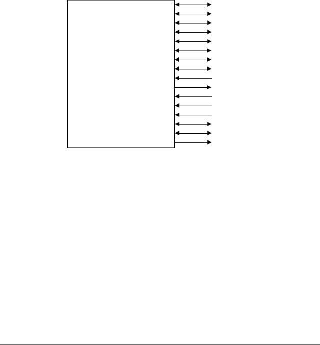
STL2 Server Board Architecture Overview |
STL2 Server Board TPS |
IRQ0/INTR |
|
|
IRQ1 |
|
|
IRQ2 |
|
|
IRQ3 |
|
|
IRQ4 |
|
|
IRQ5 |
|
|
IRQ6 |
PIC |
|
IRQ7 |
||
IB6566 |
||
IRQ8 |
||
South |
||
IRQ9/SCI |
||
Bridge |
||
IRQ10 |
||
|
||
IRQ11 |
|
|
IRQ12 |
|
|
IRQ13 |
|
|
IRQ14 |
|
|
IRQ15 |
|
|
PCIIRQ0# |
PCI |
|
PCIIRQ1# |
Interrupt |
|
PCIIRQ2# |
Router |
|
|
||
PCIIRQ3# |
IRQ3 |
|
PCIIRQ4# |
IRQ4 |
|
PCIIRQ5# |
IRQ5 |
|
PCIIRQ6# |
IRQ6 |
|
PCIIRQ7# |
IRQ7 |
|
PCIIRQ8# |
|
|
PCIIRQ9# |
IRQ9 |
|
PCIIRQ10# |
IRQ10 |
|
PCIIRQ11# |
IRQ11 |
|
PCIIRQ12# |
IRQ12 |
|
PCIIRQ13# |
|
|
PCIIRQ14# |
IRQ14 |
|
PCIIRQ15# |
IRQ15 |
Figure 2-3. STL2 Baseboard Interrupt Routing Diagram (PIC mode)
2-18
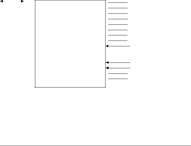
STL2 Server Board TPS |
STL2 Server Board Architecture Overview |
Timer
Keyboard
Cascade
Serial Port2/ISA
Serial Port1/ISA
ISA
Floppy/ISA
Parallel/ISA
RTC
SCI/ISA
ISA
ISA
Mouse/ISA
Coprocessor Err
P_IDE/ISA
Not Used
SCSI PORT A
SCSI PORT B
LAN
VGA
Slot02 INTA
Slot03 INTA
Slot04 INTA
Slot05 INTA
Slot06 INTA
Slot01 INTA
SLOT 02 |
03 |
04 |
05 |
06 |
01 |
|
B
C
D
IRQ0
IRQ1
IRQ2
IRQ3
IRQ4
IRQ5
IRQ6
IRQ7
IRQ8
IRQ9
IRQ10
IRQ11
IRQ12
IRQ13
IRQ14
IRQ15
PIRQ0(16)
PIRQ1(17)
PIRQ2(18)
PIRQ3(19)
PIRQ4(20)
PIRQ5(21)
PIRQ6(22)
PIRQ7(23)
PIRQ8(24)
PIRQ9(25)
PIRQ10(26)
PIRQ11(27)
PIRQ12(28)
PIRQ13(29)
PIRQ14(30)
PIRQ15(31)
Figure 2-4. STL2 Baseboard Interrupt Routing Diagram (Symmetric mode)
Revision 1.0 |
2-19 |

STL2 Server Board Architecture Overview |
STL2 Server Board TPS |
2.6.3PCI Ids
The STL2 server board PCI Ids are defined as follows:
Table 2-6. STL2 PCI IDs
|
Device |
|
|
Bus Number |
|
|
Device Number |
|
|
Slot ID Signal |
|
|
|
|
|
[23:16] |
|
|
[15:11] |
|
|
|
|
|
NB6635 North Bridge 3.0LE |
|
|
00h |
|
|
00000b |
|
|
|
|
|
|
|
|
|
|
|
|
|
|
|
|
|
ATI* Rage IIC |
|
|
00h |
|
|
00010b |
|
|
P32_AD18 |
|
|
|
|
|
|
|
|
|
|
|
|
|
|
Intel 82559 |
|
|
00h |
|
|
00011b |
|
|
P32_AD19 |
|
|
|
|
|
|
|
|
|
|
|
|
|
|
Adaptec* AIC-7899 |
|
|
00h |
|
|
00100b |
|
|
P32_AD20 |
|
|
|
|
|
|
|
|
|
|
|
|
|
|
Slot 1 (32 bit) |
|
|
00h |
|
|
00110b |
|
|
P32_AD22 |
|
|
|
|
|
|
|
|
|
|
|
|
|
|
Slot 2 (32 bit) |
|
|
00h |
|
|
00111b |
|
|
P32_AD23 |
|
|
|
|
|
|
|
|
|
|
|
|
|
|
Slot 2 (32 bit) |
|
|
00h |
|
|
01000b |
|
|
P32_AD24 |
|
|
|
|
|
|
|
|
|
|
|
|
|
|
Slot 2 (32 bit) |
|
|
00h |
|
|
01001b |
|
|
P32_AD25 |
|
|
|
|
|
|
|
|
|
|
|
|
|
|
IB6566 South Bridge |
|
|
00h |
|
|
01111b |
|
|
P32_AD31 |
|
|
|
|
|
|
|
|
|
|
|
|
|
|
Slot 2 (32 bit) |
|
|
00h |
|
|
01010b |
|
|
P32_AD26 |
|
|
|
|
|
|
|
|
|
|
|
|
|
|
Slot 2 (32 bit) |
|
|
00h |
|
|
01011b |
|
|
P32_AD27 |
|
|
|
|
|
|
|
|
|
|
|
|
|
Note:
Do not change the BUSNUM register (Offset 44h) in the NB6635 North Bridge 3.0LE from the default value.
2.6.4Relationship between PCI IRQ and PCI Device
The relationship between PCI IRQ and PCI devices are defined as follows on the STL2 server board:
|
PCI IRQ |
|
|
PCI Device |
|
|
PCI IRQ 0 |
|
|
Adaptec AIC-7899 SCSI Channel A |
|
|
|
|
|
|
|
|
PCI IRQ 1 |
|
|
Adaptec AIC-7899 SCSI Channel B |
|
|
|
|
|
|
|
|
PCI IRQ 2 |
|
|
Intel 82559 |
|
|
|
|
|
|
|
|
PCI IRQ 3 |
|
|
ATI Rage IIC |
|
|
|
|
|
|
|
|
PCI IRQ 4 |
|
|
PCI Slot 2 (INTA) |
|
|
|
|
|
|
|
|
PCI IRQ 5 |
|
|
PCI Slot 3 (INTA) |
|
|
|
|
|
|
|
|
PCI IRQ 6 |
|
|
Not Used |
|
|
|
|
|
|
|
|
PCI IRQ 7 |
|
|
PCI Slot 4 (INTA) |
|
|
|
|
|
|
|
|
PCI IRQ 8 |
|
|
PCI Slot 5 (INTA) |
|
|
|
|
|
|
|
|
PCI IRQ 9 |
|
|
PCI Slot 6 (INTA) |
|
|
|
|
|
|
|
|
PCI IRQ 10 |
|
|
PCI Slot 1 (INTA) |
|
|
|
|
|
|
|
|
PCI IRQ 11 |
|
|
PCI Slot 1 (INTB), PCI Slot 2 (INTB), PCI Slot 3 (INTC), PCI Slot 4 (INTB), PCI Slot 5 (INTC), PCI |
|
|
|
|
|
Slot 6 (INTD) |
|
|
|
|
|
|
|
|
PCI IRQ 12 |
|
|
PCI Slot 1 (INTC), PCI Slot 2 (INTC), PCI Slot 3 (INTD), PCI Slot 4 (INTC), PCI Slot 5 (INTD), PCI |
|
|
|
|
|
Slot 6 (INTB) |
|
|
|
|
|
|
|
|
PCI IRQ 13 |
|
|
PCI Slot 1 (INTD), PCI Slot 2 (INTD), PCI Slot 3 (INTB), PCI Slot 4 (INTC), PCI Slot 5 (INTD), PCI |
|
|
|
|
|
Slot 6 (INTB) |
|
|
|
|
|
|
|
2-20

STL2 Server Board TPS |
STL2 Server Board Architecture Overview |
Revision 1.0 |
2-21 |
 Loading...