

Intel T8300 - Core 2 Duo 2.4GHz 800MHz 3MB Socket P Mobile CPU, T8300 2 2.4GHz 800MHz 3MB Documentation Update
Page 1

Document Number: 320121-008
Intel® Core™2 Extreme Quad-Core Mobile
Processor,
Intel
®
Core™2 Quad Mobile Processor,
Intel® Core™2 Extreme Mobile Processor,
Intel® Core™2 Duo Mobile Processor,
Intel® Core™2 Solo Mobile Processor and
Intel® Celeron® Processor
on 45-nm Process
Specification Update
December 2011
Page 2

INFORMATION IN THIS DOCUMENT IS PROVIDED IN CONNECTION WITH INTEL® PRODUCTS. NO LICENSE, EXPRESS OR IMPLIED,
BY ESTOPPEL OR OTHERWISE, TO ANY INTELLECTUAL PROPERTY RIGHTS IS GRANTED BY THIS DOCUMENT. EXCEPT AS PROVIDED
IN INTEL'S TERMS AND CONDITIONS OF SALE FOR SUCH PRODUCTS, INTEL ASSUMES NO LIABILITY WHATSOEVER, AND INTEL
DISCLAIMS ANY EXPRESS OR IMPLIED WARRANTY, RELATING TO SALE AND/OR USE OF INTEL PRODUCTS INCLUDING LIABILITY OR
WARRANTIES RELATING TO FITNESS FOR A PARTICULAR PURPOSE, MERCHANTABILITY, OR INFRINGEMENT OF ANY PATENT,
COPYRIGHT OR OTHER INTELLECTUAL PROPERTY RIGHT.
UNLESS OTHERWISE AGREED IN WRITING BY INTEL, THE INTEL PRODUCTS ARE NOT DESIGNED NOR INTENDED FOR ANY
APPLICATION IN WHICH THE FAILURE OF THE INTEL PRODUCT COULD CREATE A SITUATION WHERE PERSONAL INJURY OR DEATH
MAY OCCUR.
Intel may make changes to specifications and product descriptions at any time, without notice. Designers must not rely on the
absence or characteristics of any features or instructions marked "reserved" or "undefined." Intel reserves these for future definition
and shall have no responsibility whatsoever for conflicts or incompatibilities arising from future changes to them. The information
here is subject to change without notice. Do not finalize a design with this information.
The products described in this document may contain design defects or errors known as errata which may cause the product to
deviate from published specifications. Current characterized errata are available on request.
Intel® processor numbers are not a measure of performance. Processor numbers differentiate featur es within each processor family,
not across different processor families. See www.intel.com/products/processor_number/ for details.
45nm products are manufactured on a lead-free process. Lead-free per EU RoHS directive July, 2006. Some E.U. RoHS exemptions
may apply to other components used in the product package. Residual amounts of halogens are below November, 2007 proposed
IPC/JEDEC J-STD-709 standards.
Intel® Active Management Technology requires the platform to have an Intel® AMT -enabled chipset, network hardware and
software, connection with a power source and a network connection.
Contact your local Intel sales office or your distributor to obtain the latest specifications and before placing your product order.
Intel, Intel Core, Intel Centrino, Intel SpeedStep, Intel386, Intel486, Pentium, Pentium Pro, Pentium 4, MMX, and the Intel logo are
trademarks of Intel Corporation in the U.S. and other countries.
*Other names and brands may be claimed as the property of others.
Copyright © 2007 - 2011, Intel Corporation. All rights reserved.
2 Specification Update
Page 3

Contents
Preface ..................................................................................................................................5
Identification Information ........................................................................................................7
Summary Tables of Changes .................................................................................................. 13
Errata ................................................................................................................................. 21
Specification Changes ........................................................................................................... 53
Specification Clarifications ..................................................................................................... 54
Documentation Changes ........................................................................................................ 56
Specification Update 3
Page 4

Revision History
Document
Number
Revision
Version
Description
Date
320121
001
1.0
Initial release
July 2008
320121
002
1.0
Updated Title
Updated Identification Information
Updated Affected Documents
Added Erratum AZ62, AZ63, AZ64,AZ65,
AZ66
August 2008
320121
003
1.0
Added Erratum AZ66-74
October 2008
320121
004
1.0
Added Erratum AZ75
Added Specification Clarification AZ2
November 2008
320121
005
1.0
Table 1 added new skus and updated E and
R step information
Errata table added R step information
March 2009
320121
006
1.0
S-SPEC updated for new E and R step in
Table 1
April 2009
320121
007
1.0
Added Erratum AZ76
December 2010
320121
008
1.0
Added Erratum AZ77
December 2011
4 Specification Update
Page 5
Document Title
Document
Number/Location
Intel® Core™2 Duo Processors and Intel® Core™2 Extreme
Processors on 45-nm Process for Platforms based on Mobile Intel®
965 Express Chipset family Datasheet
316745
Intel® Core™2 Extreme Quad-Core Mobile Processor, Intel® Core™2
Quad Mobile Processor, Intel® Core™2 Extreme Mobile Processor,
Intel® Core™2 Duo Mobile Processor, Intel® Core™2 Solo Mobile
Processor and Intel® Celeron® Processor on 45-nm Process for
Platforms based on Mobile Intel® 4 Series Express Chipset family
Datasheet
320120
Intel® Core™2 Extreme Quad-Core Processor Processors and Intel®
Core™2 Quad Processor on 45-nm Process for Platforms based on
Mobile Intel® 4 Series Express Chipset family Datasheet
320390
Intel® Celeron Processor Low Voltage and Ultra Low Voltage o 700
Series for Platforms based on Mobile Intel® GS45 Express Chipset
320389
Document Title
Document
Number/Location
Intel® 64 and IA-32 Architecture Software Developer's Manual
Documentation Changes
252046
Intel® 64 and IA-32 Architecture Software Developer’s Manual,
Volume 1: Basic Architecture
253665
Intel® 64 and IA-32 Architecture Software Developer’s Manual,
Volume 2A: Instruction Set Reference, A-M
253666
Intel® 64 and IA-32 Architecture Software Developer’s Manual,
Volume 2B: Instruction Set Reference, N-Z
253667
Intel® 64 and IA-32 Architecture Software Developer’s Manual,
253668
Preface
Preface
This document is an update to the specifications contained in the documents listed in the
following Affected Documents/Related Documents table. It is a compilation of device and
document errata, and specification clarifications and changes. This document is intended
for hardware system manufacturers and for software developers of applications,
operating system, and tools.
Information types defined in the Nomenclature section of this document are consolidated
into this update document and are no longer published in other documents. This
document may also contain information that has not been previously published.
Affected Documents
Related Documents
Specification Update 5
Page 6
Document Title
Document
Number/Location
Volume 3A: System Programming Guide
Intel® 64 and IA-32 Architecture Software Developer’s Manual,
Volume 3B: System Programming Guide
253669
IA-32 Intel® Architecture Optimization Reference Manual
248966
Intel Processor Identification and the CPUID Instruction Application
Note (AP-485)
241618
Intel® 64 and IA-32 Architectures Application Note TLBs, PagingStructure Caches, and Their Invalidation
317080
NOTE: Contact your Intel representative for the latest revision.
Nomenclature
Errata are design defects or errors. These may cause the processor behavior to deviate
from published specifications. Hardware and software designed to be used with any given
stepping must assume that all errata documented for that stepping are present on all
devices.
Preface
S-Spec Number is a five-digit code used to identify products. Products are differentiated
by their unique characteristics, e.g., core speed, L2 cache size, package type, etc. as
described in the processor identification information table. Read all notes associated with
each S-Spec number.
Specification Changes are modifications to the current published specifications. These
changes will be incorporated in any new release of the specification.
Specification Clarifications describe a specification in greater detail or further highlight
a specification‟s impact to a complex design situation. These clarifications will be
incorporated in any new release of the specification.
Documentation Changes include typos, errors, or omissions from the current published
specifications. These will be incorporated in any new release of the specification.
Note: Errata remain in the specification update throughout the product‟s lifecycle, or until a
particular stepping is no longer commercially available. Under these circumstances,
errata removed from the specification update are archived and available upon request.
Specification changes, specification clarifications and documentation changes are
removed from the specification update when the appropriate changes are made to the
appropriate product specification or user documentation (datasheets, manuals, etc.).
6 Specification Update
Page 7
Reserved
Extended
Family1
Extended
Model2
Reserved
Processor
Type3
Family
Code4
Model
Number5
Stepping
ID6
31:28
27:20
19:16
15:14
13:12
11:8
7:4
3:0
0000000b
0001b
00b
0110b
0111b
XXXXb
Identification Information
Identification Information
Component Identification via Programming Interface
Intel® Core™2 Extreme Quad-Core Mobile Processor, Intel® Core™2 Quad Mobile
Processor, Intel® Core™2 Extreme Mobile Processor, Intel® Core™2 Duo Mobile
Processor, Intel® Core™2 Solo Mobile Processor and Intel® Celeron® Processor on 45nm Process stepping can be identified by the following register contents:
When EAX is initialized to a value of 1, the CPUID instruction returns the Extended
Family, Extended Model, Type, Family, Model and Stepping value in the EAX register.
Note that the EDX processor signature value after reset is equivalent to the processor
signature output value in the EAX register.
NOTES:
1. The Extended Family, bits [27:20] are used in conjunction with the Family Code, specified in
bits [11:8], to indicate whether the processor belongs to the Intel386®, Intel486®,
Pentium®, Pentium Pro, Pentium 4, or Intel Core processor family.
2. The Extended Model, bits [19:16] in conjunction with the Model Number, specified in bits
[7:4], are used to identify the model of the processor within the processor‟s family.
3. The Processor Type, specified in bits [13:12] indicates whether the processor is an original
OEM processor, an OverDrive processor, or a dual processor (capable of being used in a dual
processor system).
4. The Family Code corresponds to bits [11:8] of the EDX register after RESET, bits [11:8] of the
EAX register after the CPUID instruction is executed with a 1 in the EAX register, and the
generation field of the Device ID register accessible through Boundary Scan.
5. The Model Number corresponds to bits [7:4] of the EDX register after RESET, bits [7:4] of the
EAX register after the CPUID instruction is executed with a 1 in the EAX register, and the
model field of the Device ID register accessible through Boundary Scan.
6. The Stepping ID in bits [3:0] indicates the revision number of that model. See Table 2 for the
processor stepping ID number in the CPUID information.
Cache and TLB descriptor parameters are provided in the EAX, EBX, ECX and EDX
registers after the CPUID instruction is executed with a 2 in the EAX register.
Specification Update 7
Page 8
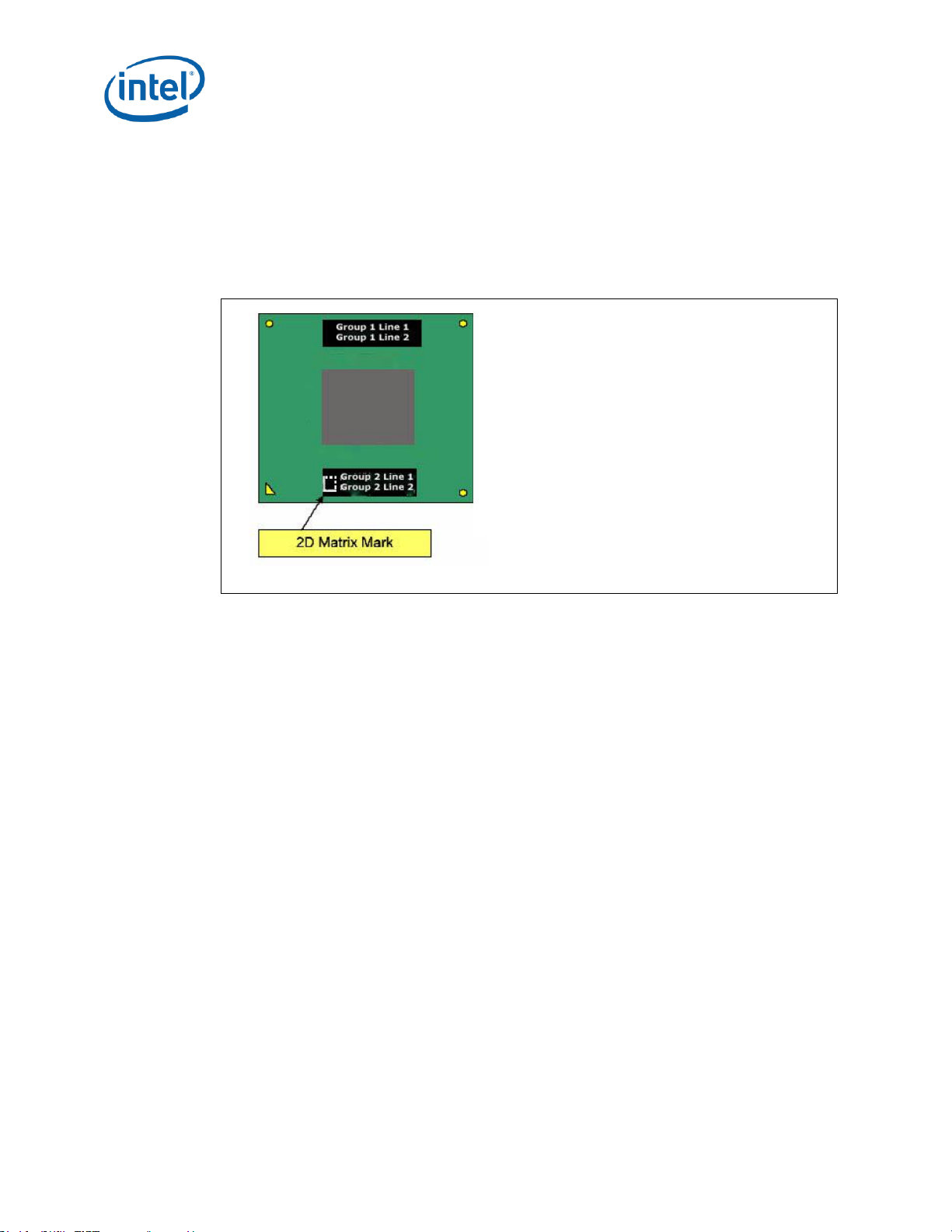
Component Marking Information
MARK EXAMPLE: Group
1 Line 1: Unit Identifier Processor #
Group 1 Line 2: FPO SSPEC#
Group 2 Line 1: Frequency/L2 Cache/FSB Speed
Group 2 Line 2: INTEL (m) © ’07
The processor stepping can be identified by the following component markings:
Figure 1. Processor S-Spec Top-side Markings (Example)
Identification Information
8 Specification Update
Page 9

S-
Spec#
Processor
#
Package
Processor
Stepping
CPUID
Core Frequency
HFM/LFM/ SLFM
(GHz)
FSB Freq.
(MHz)
IDAT
Freq.(GHz)
HFM TDP
(W)
L2
Cache(MB)
Notes
SLAQH
T9500
m-FCPGA
C-0
000010676h
2.6/1.2/0.8
800
2.8
35 6 2,3,4
SLAPW
T9500
m-FCBGA
C-0
000010676h
2.6/1.2/0.8
800
2.8
35 6 2,3,4
SLAQG
T9300
m-FCPGA
C-0
000010676h
2.5/1.2/0.8
800
2.7
35 6 2,3,4
SLAPV
T9300
m-FCBGA
C-0
000010676h
2.5/1.2/0.8
800
2.7
35 6 2,3,4
SLAPU
T8300
m-FCBGA
C-0
000010676h
2.4/1.2/0.8
800
2.6
35 3 2,3,4
SLAUU
T8100
m-FCPGA
C-0
000010676h
2.1/1.2/0.8
800
2.3
35 3 2,3,4
SLAPT
T8100
m-FCBGA
C-0
000010676h
2.1/1.2/0.8
800
2.3
35 3 2,3,4
SLAPA
T8300
m-FCPGA
M-0
000010676h
2.4/1.2/0.8
800
2.6
35 3 2,3,4
SLAPR
T8300
m-FCBGA
M-0
000010676h
2.4/1.2/0.8
800
2.6
35 3 2,3,4
SLAP9
T8100
m-FCPGA
M-0
000010676h
2.1/1.2/0.8
800
2.3
35 3 2,3,4
SLAPS
T8100
m-FCBGA
M-0
000010676h
2.1/1.2/0.8
800
2.3
35 3 2,3,4
SLAVJ
T8100
m-FCPGA
M-0
000010676h
2.1/1.2/0.8
800
2.3
35 3 2,3,4
SLAXG
T8100
m-FCPGA
M-0
000010676h
2.1/1.2/0.8
800
2.3
35 3 2,3,4
SLAZD
T8100
m-FCPGA
M-0
000010676h
2.1/1.2/0.8
800
2.3
35 3 2,3,4,7
SLAYZ
T8100
m-FCPGA
M-0
000010676h
2.1/1.2/0.8
800
2.3
35 3 2,3,4,7
SLAZC
T8300
m-FCPGA
M-0
000010676h
2.4/1.2/0.8
800
2.6
35 3 2,3,4,7
SLAZB
T9300
m-FCPGA
C-0
000010676h
2.5/1.2/0.8
800
2.7
35 6 2,3,4,7
SLAYY
T9300
m-FCPGA
C-0
000010676h
2.5/1.2/0.8
800
2.7
35 6 2,3,4,7
SLAZA
T9500
m-FCPGA
C-0
000010676h
2.6/1.2/0.8
800
2.8
35 6 2,3,4,7
SLAYX
T9500
m-FCPGA
C-0
000010676h
2.6/1.2/0.8
800
2.8
35 6 2,3,4,7
SLAQJ
X9000
m-FCPGA
C-0
000010676h
2.8/1.2/0.8
800
N/A
44 6 1,5,6
SLAZ3
X9000
m-FCPGA
C-0
000010676h
2.8/1.2/0.8
800
N/A
44 6 1,5,6,7
SLB47
T9600
m-FCPGA
C-0
000010676h
2.80/1.6/0.8
1066
2.93
35 6 4,6,10
SLB43
T9600
m-FCBGA
C-0
000010676h
2.80/1.6/0.8
1066
2.93
35 6 4,6,10
SLB46
T9400
m-FCPGA
C-0
000010676h
2.53/1.6/0.8
1066
2.66
35 6 4,6,10
SL3BX
T9400
m-FCBGA
C-0
000010676h
2.53/1.6/0.8
1066
2.66
35 6 4,6,10
SLB4E
P9500
m-FCPGA
C-0
000010676h
2.53/1.6/0.8
1066
2.66
25 6 6,11,12
SL3BW
P9500
m-FCBGA
C-0
000010676h
2.53/1.6/0.8
1066
2.66
25 6 6,11,12
SLB3S
P8600
m-FCPGA
M-0
000010676h
2.40/1.6/0.8
1066
2.53
25 3 6,11,12
SLB4N
P8600
m-FCBGA
M-0
000010676h
2.40/1.6/0.8
1066
2.53
25 3 6,11,12
SLB3R
P8400
m-FCPGA
M-0
000010676h
2.26/1.6/0.8
1066
2.40
25 3 6,11,12
Identification Information
Table 1. Processor Identification Information
Specification Update 9
Page 10

Identification Information
S-
Spec#
Processor
#
Package
Processor
Stepping
CPUID
Core Frequency
HFM/LFM/ SLFM
(GHz)
FSB Freq.
(MHz)
IDAT
Freq.(GHz)
HFM TDP
(W)
L2
Cache(MB)
Notes
SLB4M
P8400
m-FCBGA
M-0
000010676h
2.26/1.6/0.8
1066
2.40
25 3 6,11,12
SLB3Q
P8400
m-FCPGA
M-0
000010676h
2.26/1.6/0.8
1066
2.40
25 3 26,8,9
SL3BV
P8600
m-FCBGA
C-0
000010676h
2.40/1.6/0.8
1066
2.53
25 3 6,11,12
SL3BU
P8400
m-FCBGA
C-0
000010676h
2.26/1.6/0.8
1066
2.40
25 3 6,11,12
SLB48
X9100
m-FCPGA
C-0
000010676h
3.06/1.6/0.8
1066
N/A
44 6 1,5,6
SLAYS
T8300
m-FCPGA
M-0
000010676h
2.4/1.2/0.8
800
2.6
35 3 2,3,4,7
SLAYU
T8100
m-FCPGA
M-0
000010676h
2.1/1.2/0.8
800
2.3
35 3 2,3,4,7
SLAYP
T8100
m-FCPGA
M-0
000010676h
2.1/1.2/0.8
800
2.3
35 3 2,3,4,7
SLAYQ
T8300
m-FCPGA
M-0
000010676h
2.4/1.2/0.8
800
2.6
35 3 2,3,4,7
SLG8E
P7350
m-FCBGA
C-0
000010676h
2.00/1.6/0.8
1066
N/A
25 3 17,6,18
SLB45
P7450
m-FCPGA
C-0
000010676h
2.13/1.6/0.8
1066
N/A
25 3 17,6,18
SLB44
P7350
m-FCPGA
C-0
000010676h
2.00/1.6/0.8
1066
N/A
25 3 17,6,18
SLB54
P7450
m-FCPGA
M-0
000010676h
2.13/1.6/0.8
1066
N/A
25 3 17,6,18
SLB53
P7350
m-FCPGA
M-0
000010676h
2.00/1.6/0.8
1066
N/A
25 3 17,6,18
SLB5J
QX9300
m-FCPGA
E-0
00001067Ah
2.53/1.6/(n/a)
1066
2.8
45
12
14,15,16
SLB5G
Q9100
m-FCPGA
E-0
00001067Ah
2.26/1.6/(n/a)
1066
2.53
45
12
14,15,16
SLB64
SP9400
m-FCBGA
C-0
000010676h
2.40/1.6/0.8
1066
2.53
25 6 17,6,18
SLB63
SP9300
m-FCBGA
C-0
000010676h
2.26/1.6/0.8
1066
2.40
25 6 17,6,18
SLB66
SL9400
m-FCBGA
C-0
000010676h
1.86/1.6/0.8
1066
2.13
17 6 19,6,20
SLB65
SL9300
m-FCBGA
C-0
000010676h
1.60/0.8/0.8
1066
1.86
17 6 19,6,20
SLB5V
SU9400
m-FCBGA
M-0
000010676h
1.40/0.8/0.8
800
1.60
10 3 21,22,23
SLB5Q
SU9300
m-FCBGA
M-0
000010676h
1.20/0.8/0.8
800
1.40
10 3 21,22,23
SLGAR
SU3300
m-FCBGA
M-0
000010676h
1.20/0.8/(n/a)
800
N/A
5.5 3 24,13
SLGAS
723
m-FCBGA
M-0
000010676h
1.20/(n/a)/(n/a)
800
N/A
10 1 25,13
QJPQ
SU9600
m-FCBGA
R-0
00001067Ah
1.6/1.2/0.8
800
1.8
10 3 31,32,33
QJPM
SU9400
m-FCBGA
R-0
00001067Ah
1.4/1.2/0.8
800
1.6
10 3 31,32,33
QJPF
SU9300
m-FCBGA
R-0
00001067Ah
1.2/1.2/0.8
800
1.4
10 3 31,32,33
QJNG
SL9600
m-FCBGA
E-0
00001067Ah
2.13/1.6/0.8
1066
2.4
17 6 29,11,30
QJND
SL9400
m-FCBGA
E-0
00001067Ah
1.86/1.6/0.8
1066
2.13
17 6 29,11,30
QJNA
SL9300
m-FCBGA
E-0
00001067Ah
1.6/1.6/0.8
1066
1.86
17 6 29,11,30
QJNR
SP9600
m-FCBGA
E-0
00001067Ah
2.53/1.6/0.8
1066
2.66
25 6 27,11,28
QJNN
SP9400
m-FCBGA
E-0
00001067Ah
2.4/1.6/0.8
1066
2.53
25 6 27,11,28
QJNK
SP9300
m-FCBGA
E-0
00001067Ah
2.26/1.6/0.8
1066
2.4
25 6 27,11,28
10 Specification Update
Page 11

S-
Spec#
Processor
#
Package
Processor
Stepping
CPUID
Core Frequency
HFM/LFM/ SLFM
(GHz)
FSB Freq.
(MHz)
IDAT
Freq.(GHz)
HFM TDP
(W)
L2
Cache(MB)
Notes
QJNW
723
m-FCBGA
R-0
00001067Ah
1.2/(n/a)/(n/a)
800
N/A
10 1 35,13
QJPT
SU3300
m-FCBGA
R-0
00001067Ah
1.2/1.2/0.8
800
N/A
5.5 3 34,13
QJRU
743
m-FCBGA
R-0
00001067Ah
1.3/(n/a)/(n/a)
800
N/A
10 1 35,13
QKUS
SU3500
m-FCBGA
R-0
00001067Ah
1.4/1.2/0.8
800
N/A
5.5 3 34,13
SLGFN
SU9600
m-FCBGA
R-0
00001067Ah
1.6/1.2/0.8
800
1.8
10 3 31,32,33
SLGAK
SU9400
m-FCBGA
R-0
00001067Ah
1.4/1.2/0.8
800
1.6
10 3 31,32,33
SLGAL
SU9300
m-FCBGA
R-0
00001067Ah
1.2/1.2/0.8
800
1.4
10 3 31,32,33
SLGEQ
SL9600
m-FCBGA
E-0
00001067Ah
2.13/1.6/0.8
1066
2.4
17 6 29,6,30
SLGAB
SL9400
m-FCBGA
E-0
00001067Ah
1.86/1.6/0.8
1066
2.13
17 6 29,6,30
SLGAG
SL9300
m-FCBGA
E-0
00001067Ah
1.6/1.6/0.8
1066
1.86
17 6 29,6,30
SLGER
SP9600
m-FCBGA
E-0
00001067Ah
2.53/1.6/0.8
1066
2.66
25 6 27,6,28
SLGAA
SP9400
m-FCBGA
E-0
00001067Ah
2.4/1.6/0.8
1066
2.53
25 6 27,6,28
SLGAF
SP9300
m-FCBGA
E-0
00001067Ah
2.26/1.6/0.8
1066
2.4
25 6 27,6,28
SLGAM
723
m-FCBGA
R-0
00001067Ah
1.2/(n/a)/(n/a)
800
N/A
10 1 35,13
SLGAJ
SU3300
m-FCBGA
R-0
00001067Ah
1.2/1.2/0.8
800
N/A
5.5 3 34,13
SLGEV
743
m-FCBGA
R-0
00001067Ah
1.3/(n/a)/(n/a)
800
N/A
10 1 35,13
SLGQQ
SU3500
m-FCBGA
R-0
00001067Ah
1.4/1.2/0.8
800
N/A
5.5 3 34,13
Identification Information
NOTES:
1. Does not support Intel® Dynamic Acceleration Technology
2. Vcc core VID=1.000-1.250/0.850-1.250 V [HFM/LFM]; 0.750-0.925 V [S-LFM]
3. Vcc core VID=0.650-0.859/0.600-0.850/0.350-0.700 V [C4/DC4/C6]
4. Vcc core VID=1.000-1.300 [IDAT]
5. Vcc core VID=1.000-1.275/0.850-1.100 V [HFM/LFM]; 0.800-1.000 V [S-LFM]
6. Vcc core VID=0.650-0.850/0.600-0.850/0.35-0.70 V [C4/DC4/C6]
7. This part is screened to avoid Erratum AZ52
8. Vcc core VID=1.050-1.1625/1.000 V [HFM/LFM]; 0.825-0.950 V [S-LFM]
9. Vcc core VID=1.050-1.2125 [IDAT]
10. Vcc core VID=1.000-1.250/0.850-1.100 V [HFM/LFM]; 0.750-0.950 V [S-LFM]
11. Vcc core VID=0.900-1.250/0.850-1.025 V [HFM/LFM]; 0.750-0.950 V [S-LFM]
12. Vcc core VID=0.900-1.300 [IDAT]
13. Intel® Celeron® M processor
14. Vcc core VID=0.90-1.25/0.850-1.100 V [HFM/LFM]
15. Vcc core VID=0.65-0.85 [C4]
16. Vcc core VID=0.90-1.30 [IDAT]
17. Vcc core VID=0.900-1.2125/0.850-1.025 V [HFM/LFM]; 0.75-0.95 V [S-LFM]
18. Vcc core VID=0.900-1.275 [IDAT]
19. Vcc core VID=0.900-1.175/0.850-1.025 V [HFM/LFM]; 0.75-0.95 V [S-LFM]
20. Vcc core VID=0.90-1.25 [IDAT]
21. Vcc core VID=0.775-1.100/0.80-0.975 V [HFM/LFM]; 0.750-0.925 V [S-LFM]
22. Vcc core VID=0.65-0.80/0.60-0.80/0.35-0.60 V [C4/DC4/C6]
23. Vcc core VID=0.80-1.1625 [IDAT]
24. Vcc core VID=0.80-1.25 [VID]
25. Vcc core VID=0.775-1.10 [VID]
Specification Update 11
Page 12

26. Vcc core VID=0.725-0.775/0.725-0.750/0.400-0.700 V [C4/DC4/C6]
27. Vcc core VID=0.900-1.2125/0.850-1.025 V [HFM/LFM]; 0.75-0.95 V [S-LFM]
28. Vcc core VID=0.900-1.275 [IDAT]
29. Vcc core VID=0.900-1.175/0.850-1.025 V [HFM/LFM]; 0.75-0.95 V [S-LFM]
30. Vcc core VID=0.90-1.25 [IDAT]
31. Vcc core VID=0.775-1.100/0.80-0.975 V [HFM/LFM]; 0.750-0.925 V [S-LFM]
32. Vcc core VID=0.65-0.80/0.60-0.80/0.35-0.60 V [C4/DC4/C6]
33. Vcc core VID=0.80-1.1625 [IDAT]
34. Vcc core VID=0.80-1.25 [VID]
35. Vcc core VID=0.775-1.10 [VID]
36. Vcc core VID=0.900-1.2125/0.850-1.025 V [HFM/LFM]; 0.75-0.95 V [S-LFM]
37. Vcc core VID=0.900-1.2125/0.850-1.025 V [HFM/LFM]; 0.75-0.95 V [S-LFM]
38. Vcc core VID=0.900-1.175/0.850-1.025 V [HFM/LFM]; 0.75-0.95 V [S-LFM]
§
Identification Information
12 Specification Update
Page 13

Summary Tables of Changes
Summary Tables of Changes
The following table indicates the Specification Changes, Errata, Specification
Clarifications or Documentation Changes, which apply to the listed CPU steppings. Intel
intends to fix some of the errata in a future stepping of the component, and to account
for the other outstanding issues through documentation or Specification Changes as
noted. This table uses the following notations:
Codes Used in Summary Table
Stepping
X: Erratum, Specification Change or Clarification that applies to
this stepping.
Status
Row
(No mark) or (Blank Box): This erratum is fixed in listed stepping or specification change
does not apply to listed stepping.
Doc: Document change or update that will be implemented.
PlanFix: This erratum may be fixed in a future stepping of the
product.
Fixed: This erratum has been previously fixed.
NoFix: There are no plans to fix this erratum.
Shaded: This item is either new or modified from the previous version
of the document.
Specification Update 13
Page 14

Summary Tables of Changes
Note: Each Specification Update item is prefixed with a capital letter to distinguish the product.
The key below details the letters that are used in Intel‟s microprocessor Specification
Updates:
A = Dual-Core Intel® Xeon® processor 7000 sequence
C = Intel® Celeron® processor
D = Dual-Core Intel® Xeon® processor 2.80 GHz
E = Intel® Pentium® III processor
F = Intel® Pentium® processor Extreme Edition and Intel® Pentium® D processor
I = Dual-Core Intel® Xeon® processor 5000 series
J = 64-bit Intel® Xeon® processor MP with 1-MB L2 Cache
K = Mobile Intel® Pentium® III processor
L = Intel® Celeron® D processor
M = Mobile Intel® Celeron® processor
N = Intel® Pentium® 4 processor
O = Intel® Xeon® processor MP
P = Intel® Xeon® processor
Q = Mobile Intel® Pentium® 4 processor supporting Hyper-Threading Technology on 90nm process technology
R = Intel® Pentium® 4 processor on 90 nm process
S = 64-bit Intel® Xeon® processor with 800 MHz system bus (1 MB and 2 MB L2 cache
versions)
T = Mobile Intel® Pentium® 4 processor–M
U = 64-bit Intel® Xeon® processor MP with up to 8MB L3 Cache
V = Mobile Intel® Celeron® processor on .13 Micron Process in Micro-FCPGA Package
W= Intel® Celeron®-M processor
X = Intel® Pentium® M processor on 90-nm process with 2-MB L2 cache and Intel®
Processors A100 and A110 with 512-KB L2 cache
Y = Intel® Pentium® M processor
Z = Mobile Intel® Pentium® 4 processor with 533 MHz system bus
AA= Intel® Pentium® D Processor 900 Sequence and Intel® Pentium® processor
Extreme Edition 955, 965
AB= Intel® Pentium® 4 processor 6x1 Sequence
AC= Intel® Celeron® processor in 478 pin package
AD = Intel® Celeron® D processor on 65 nm process
AE = Intel® Core™ Duo processor and Intel® Core™ Solo processor on 65nm process
AF = Dual-Core™ Intel® Xeon® processor LV
AG = Dual-Core Intel® Xeon® processor 5100 Series
AH= Intel® Core™2 Duo mobile processor
AI = Intel® Core™2 Extreme processor X6800
Δ
and Intel® Core™2 Duo Desktop
processor E6000 and E4000 Sequence
AJ = Quad-Core Intel® Xeon® processor 5300 Series
AK = Intel® Core™2 Extreme quad-core processor QX6700 and Intel® Core™2 Quad
processor Q6600
AL = Dual-Core Intel® Xeon® processor 7100 Series
14 Specification Update
Page 15

Summary Tables of Changes
AM = Intel® Celeron® processor 400 sequence
AN = Intel® Pentium® Dual-Core processor
AO = Quad-Core Intel® Xeon® processor 3200 Series
AP = Dual-Core Intel® Xeon® processor 3000 Series
AQ = Intel® Pentium® Dual-Core Desktop Processor E2000 Sequence
AR = Intel® Celeron® processor 500 series
AS = Intel® Xeon® processor 7200, 7300 series
AT = Intel® Celeron® processor 200 series
AU = Intel® Celeron® Dual Core processor T1400
AV = Intel® Core™2 Extreme processor QX9000 sequence and Intel® Core™2 Quad
processor Q9000 sequence processor
AW = Intel® Core™ 2 Duo
AX =Quad-Core Intel® Xeon® processor 5400 series
AY =Dual-Core Intel® Xeon® processor 5200 series
AZ = Intel® Core™2 Extreme Quad-Core Mobile Processor, Intel® Core™2 Quad Mobile
Processor, Intel® Core™2 Extreme Mobile Processor, Intel® Core™2 Duo Mobile
Processor, Intel® Core™2 Solo Mobile Processor and Intel® Celeron® Processor on 45-
nm Process
AAA = Quad-Core Intel® Xeon® processor 3300 series
AAB = Dual-Core Intel® Xeon® E3110 Processor
AAC = Intel® Celeron® dual-core processor E1000 series
AAD = Intel® CoreTM2 Extreme Processor QX9775
AAE = Intel® AtomTM processor Z5xx series
AAF = Intel® AtomTM processor 200 series
AAG = Intel® Atom™ processor N series
AAH = Intel® Atom™ processor 300 series
Note: Intel processor numbers are not a measure of performance. Processor numbers
differentiate features within each processor family, not across different processor
families. See http://www.intel.com/products/processor_number for details.
Specification Update 15
Page 16

Errata
Number
Steppings
Status
ERRATA
C-0
M-0
E-0
R-0
AZ1
X X X X No Fix
EFLAGS Discrepancy on a Page Fault After a Multiprocessor
TLB Shootdown
AZ2
X X X X No Fix
INVLPG Operation for Large (2M/4M) Pages May be
Incomplete under Certain Conditions
AZ3
X X X X No Fix
Store to WT Memory Data May be Seen in Wrong Order by
Two Subsequent Loads
AZ4
X X X X No Fix
Non-Temporal Data Store May be Observed in Wrong
Program Order
AZ5
X X X X No Fix
Page Access Bit May be Set Prior to Signaling a Code
Segment Limit Fault
AZ6
X X X X No Fix
Updating Code Page Directory Attributes without TLB
Invalidation May Result in Improper Handling of Code #PF
AZ7
X X X X No Fix
Storage of PEBS Record Delayed Following Execution of
MOV SS or STI
AZ8
X X X X No Fix
Performance Monitoring Event FP_MMX_TRANS_TO_MMX
May Not Count Some Transitions
AZ9
X X X X No Fix
A REP STOS/MOVS to a MONITOR/MWAIT Address Range
May Prevent Triggering of the Monitoring Hardware
AZ10
X X X X No Fix
Performance Monitoring Event MISALIGN_MEM_REF May
Over Count
AZ11
X X X X No Fix
The Processor May Report a #TS Instead of a #GP Fault
AZ12
X X X X No Fix
Code Segment Limit Violation May Occur on 4 Gigabyte
Limit Check
AZ13
X X X X No Fix
A Write to an APIC Register Sometimes May Appear to
Have Not Occurred
AZ14
X X X X No Fix
Last Branch Records (LBR) Updates May be Incorrect after
a Task Switch
AZ15
X X X X No Fix
REP MOVS/STOS Executing with Fast Strings Enabled and
Crossing Page Boundaries with Inconsistent Memory Types
may use an Incorrect Data Size or Lead to MemoryOrdering Violations.
AZ16
X X X X No Fix
Upper 32 bits of 'From' Address Reported through BTMs or
BTSs May be Incorrect
AZ17
X X X X No Fix
Address Reported by Machine-Check Architecture (MCA) on
Single-bit L2 ECC Errors May be Incorrect
AZ18
X X X X No Fix
Code Segment Limit/Canonical Faults on RSM May be
Serviced before Higher Priority Interrupts/Exceptions
AZ19
X X X X No Fix
Store Ordering May be Incorrect between WC and WP
Memory Type
Summary Tables of Changes
16 Specification Update
Page 17

Number
Steppings
Status
ERRATA
C-0
M-0
E-0
R-0
AZ20
X X X X No Fix
EFLAGS, CR0, CR4 and the EXF4 Signal May be Incorrect
after Shutdown
AZ21
X X X X No Fix
Premature Execution of a Load Operation Prior to Exception
Handler Invocation
AZ22
X X X X No Fix
Performance Monitoring Events for Retired Instructions
(C0H) May Not Be Accurate
AZ23
X X X X No Fix
Returning to Real Mode from SMM with EFLAGS.VM Set May
Result in Unpredictable System Behavior
AZ24
X X X X No Fix
CMPSB, LODSB, or SCASB in 64-bit Mode with Count
Greater or Equal to 248 May Terminate Early
AZ25
X X X X No Fix
Writing the Local Vector Table (LVT) when an Interrupt is
Pending May Cause an Unexpected Interrupt
AZ26
X X X X No Fix
Pending x87 FPU Exceptions (#MF) Following STI May Be
Serviced Before Higher Priority Interrupts
AZ27
X X X X No Fix
VERW/VERR/LSL/LAR Instructions May Unexpectedly
Update the Last Exception Record (LER) MSR
AZ28
X X X X No Fix
INIT Does Not Clear Global Entries in the TLB
AZ29
X X X X No Fix
Split Locked Stores May not Trigger the Monitoring
Hardware
AZ30
X X X X No Fix
Programming the Digital Thermal Sensor (DTS) Threshold
May Cause Unexpected Thermal Interrupts
AZ31
X X X X No Fix
Writing Shared Unaligned Data that Crosses a Cache Line
without Proper Semaphores or Barriers May Expose a
Memory Ordering Issue
AZ32
X X X X No Fix
General Protection (#GP) Fault May Not Be Signaled on
Data Segment Limit Violation above 4-G Limit
AZ33
X X X X No Fix
An Asynchronous MCE During a Far Transfer May Corrupt
ESP
AZ34
X X X X Plan
Fix
CPUID Reports Architectural Performance Monitoring
Version 2 is Supported, When Only Version 1 Capabilities
are Available
AZ35
X X X X No Fix
B0-B3 Bits in DR6 May Not be Properly Cleared After Code
Breakpoint
AZ36
X X X X No Fix
An xTPR Update Transaction Cycle, if Enabled, May be
Issued to the FSB after the Processor has Issued a StopGrant Special Cycle
AZ37
X X X X Plan
Fix
Performance Monitoring Event IA32_FIXED_CTR2 May Not
Function Properly when Max Ratio is a Non-Integer Coreto-Bus Ratio
AZ38
X X X X No Fix
Instruction Fetch May Cause a Livelock During Snoops of
the L1 Data Cache
AZ39
X X X X No Fix
Use of Memory Aliasing with Inconsistent Memory Type
may Cause a System Hang or a Machine Check Exception
Summary Tables of Changes
Specification Update 17
Page 18

Summary Tables of Changes
Number
Steppings
Status
ERRATA
C-0
M-0
E-0
R-0
AZ40
X X X X No Fix
A WB Store Following a REP STOS/MOVS or FXSAVE May
Lead to Memory-Ordering Violations
AZ41
X X X X Plan
Fix
VM Exit with Exit Reason "TPR Below Threshold" Can Cause
the Blocking by MOV/POP SS and Blocking by STI Bits to be
Cleared in the Guest Interruptibility-State Field
AZ42
X X X X No Fix
Using Memory Type Aliasing with Cacheable and WC
Memory Types May Lead to Memory Ordering Violations
AZ43
X X X X No Fix
VM Exit Caused by a SIPI Results in Zero Being Saved to
the Guest RIP Field in the VMCS
AZ44
X X X X No Fix
NMIs May Not Be Blocked by a VM-Entry Failure
AZ45
X X X X Plan
Fix
Partial Streaming Load Instruction Sequence May Cause
the Processor to Hang
AZ46
X X X X Plan
Fix
Self/Cross Modifying Code May Not be Detected or May
Cause a Machine Check Exception
AZ47
X X X X Plan
Fix
Data TLB Eviction Condition in the Middle of a Cacheline
Split Load Operation May Cause the Processor to Hang
AZ48
X X X X Plan
Fix
Update of Read/Write (R/W) or User/Supervisor (U/S) or
Present (P) Bits without TLB Shootdown May Cause
Unexpected Processor Behavior
AZ49
X X X X Plan
Fix
RSM Instruction Execution under Certain Conditions May
Cause Processor Hang or Unexpected Instruction Execution
Results
AZ50
X X X X No Fix
Benign Exception after a Double Fault May Not Cause a
Triple Fault Shutdown
AZ51
X X X X No Fix
LER MSRs May Be Incorrectly Updated
AZ52
X X X X Plan
Fix
Processor May Unexpectedly Assert False THERMTRIP#
After Receiving a Warm Reset
AZ53
X X X X Plan
Fix
Short Nested Loops That Span Multiple 16-Byte Boundaries
May Cause a Machine Check Exception or a System Hang
AZ54
X X X X No Fix
IA32_MC1_STATUS MSR Bit[60] Does Not Reflect Machine
Check Error Reporting Enable Correctly
AZ55
X X X X No Fix
An Enabled Debug Breakpoint or Single Step Trap May Be
Taken after MOV SS/POP SS Instruction if it is Followed by
an Instruction That Signals a Floating Point Exception
AZ56
X X X X No Fix
Code Segment Limit/Canonical Faults on RSM May be
Serviced before Higher Priority Interrupts/Exceptions and
May Push the Wrong Address Onto the Stack
AZ57
X X X X No Fix
A VM Exit Due to a Fault While Delivering a Software
Interrupt May Save Incorrect Data into the VMCS
AZ58
X X X X No Fix
A VM Exit Occurring in IA-32e Mode May Not Produce a
VMX Abort When Expected
AZ59
X X X X No Fix
IRET under Certain Conditions May Cause an Unexpected
Alignment Check Exception
18 Specification Update
Page 19

Number
Steppings
Status
ERRATA
C-0
M-0
E-0
R-0
AZ60
X X X X No Fix
Thermal Interrupts are Dropped During and While Exiting
Intel® Deep Power-Down State
AZ61
X X X X No Fix
VM Entry May Fail When Attempting to Set
IA32_DEBUGCTL.FREEZE_WHILE_SMM_EN
AZ62
X X No Fix
VM Entry May Use Wrong Address to Access Virtual-APIC
Page
AZ63
X X No Fix
INIT Incorrectly Resets IA32_LSTAR MSR
AZ64
X X No Fix
When a CPUID instruction is executed, the returned EAX,
EBX, ECX, and/or EDX may be incorrect.
AZ65
X X X X No Fix
Global Instruction TLB Entries May Not be Invalidated on a
VM Exit or VM Entry
AZ66
X X No Fix
XRSTOR Instruction May Cause Extra Memory Reads
AZ67
X X X X No Fix
LBR, BTS, BTM May Report a Wrong Address when an
Exception/Interrupt Occurs in 64-bit Mode
AZ68
X X No Fix
When Intel® Deep Power-Down State is Being Used,
IA32_FIXED_CTR2 May Return Incorrect Cycle Counts
AZ69
X X No Fix
Enabling PECI via the PECI_CTL MSR Incorrectly
Writes CPUID_FEATURE_MASK1 MSR
AZ70
X X X X No Fix
Corruption of CS Segment Register During RSM While
Transitioning From Real Mode to Protected Mode
AZ71
X X No Fix
The XSAVE Instruction May Erroneously Set Reserved Bits
in the XSTATE_BV Field
AZ72
X X No Fix
Store Ordering Violation When Using XSAVE
AZ73
X X X X No Fix
Memory Ordering Violation With Stores/Loads Crossing a
Cacheline Boundary
AZ74
X X No Fix
The XRSTOR Instruction May Fail to Cause a GeneralProtection Exception
AZ75
X X X X No Fix
B0-B3 Bits in DR6 For Non-Enabled Breakpoints May be
Incorrectly Set
AZ76
X X X X No Fix
A 64-bit Register IP-relative Instruction May Return
Unexpected Results
AZ77
X X X X No Fix
Intel® Trusted Execution Technology ACM Revocation
Number
SPECIFICATION CHANGES
There are no Specification Changes in this Specification Update revision
Summary Tables of Changes
Specification Update 19
Page 20

Number
SPECIFICATION CLARIFICATIONS
AZ1
Clarification of Translation Lookaside Buffers (TLBS) Invalidation
AZ2
CPUID Instruction Will Return Brand String With a Missing Letter
Number
DOCUMENTATION CHANGES
There are no Documentation Changes in this Specification Update revision.
Summary Tables of Changes
§
20 Specification Update
Page 21

Errata
Errata
AZ1. EFLAGS Discrepancy on a Page Fault after a Multiprocessor TLB
Shootdown
Problem: This erratum may occur when the processor executes one of the following read-modify-
write arithmetic instructions and a page fault occurs during the store of the memory
operand: ADD, AND, BTC, BTR, BTS, CMPXCHG, DEC, INC, NEG, NOT, OR, ROL/ROR,
SAL/SAR/SHL/SHR, SHLD, SHRD, SUB, XOR, and XADD. In this case, the EFLAGS value
pushed onto the stack of the page fault handler may reflect the status of the register
after the instruction would have completed execution rather than before it. The following
conditions are required for the store to generate a page fault and call the operating
system page fault handler:
1. The store address entry must be evicted from the DTLB by speculative loads from
other instructions that hit the same way of the DTLB before the store has
completed. DTLB eviction requires at least three-load operations that have linear
address bits 15:12 equal to each other and address bits 31:16 different from
each other in close physical proximity to the arithmetic operation.
2. The page table entry for the store address must have its permissions tightened
during the very small window of time between the DTLB eviction and execution of
the store. Examples of page permission tightening include from Present to Not
Present or from Read/Write to Read Only, etc.
3. Another processor, without corresponding synchronization and TLB flush, must
cause the permission change.
Implication: This scenario may only occur on a multiprocessor platform running an operating system
that performs “lazy” TLB shootdowns. The memory image of the EFLAGS register on the
page fault handler's stack prematurely contains the final arithmetic flag values although
the instruction has not yet completed. Intel has not identified any operating systems that
inspect the arithmetic portion of the EFLAGS register during a page fault nor observed
this erratum in laboratory testing of software applications.
Workaround: No workaround is needed upon normal restart of the instruction, since this erratum is
transparent to the faulting code and results in correct instruction behavior. Operating
systems may ensure that no processor is currently accessing a page that is scheduled to
have its page permissions tightened or have a page fault handler that ignores any
incorrect state.
Status: For the steppings affected, see the Summary Tables of Changes.
Specification Update 21
Page 22

Errata
AZ2. INVLPG Operation for Large (2M/4M) Pages May Be Incomplete under
Certain Conditions
Problem: The INVLPG instruction may not completely invalidate Translation Look-aside Buffer
(TLB) entries for large pages (2M/4M) when both of the following conditions exist:
“Address range of the page being invalidated spans several Memory Type Range
Registers (MTRRs) with different memory types specified “INVLPG operation is
preceded by a Page Assist Event (Page Fault (#PF) or an access that results in either A
or D bits being set in a Page Table Entry (PTE))
Implication: Stale translations may remain valid in TLB after a PTE update resulting in unpredictable
system behavior. Intel has not observed this erratum with any commercially available
software.
Workaround: Software should ensure that the memory type specified in the MTRRs is the same for the
entire address range of the large page.
Status: For the steppings affected, see the Summary Tables of Changes.
AZ3. Store to WT Memory Data May be Seen in Wrong Order by Two,
Subsequent Loads
Problem: When data of Store to WT memory is used by two, subsequent loads of one thread, and
another thread performs cacheable write to the same address, the first load may get the
data from external memory or L2 written by another core, while the second load will get
the data straight from the WT Store.
Implication: Software that uses WB to WT memory aliasing may violate proper store ordering.
Workaround: Do not use WB to WT aliasing.
Status: For the steppings affected, see the Summary Tables of Changes.
AZ4. Non-Temporal Data Store May Be Observed in Wrong Program Order
Problem: When non-temporal data is accessed by multiple read operations in one thread while
another thread performs a cacheable write operation to the same address, the data
stored may be observed in wrong program order (i.e., later load operations may read
older data).
Implication: Software that uses non-temporal data without proper serialization before accessing the
non-temporal data may observe data in wrong program order.
Workaround: Software that conforms to the Intel® 64 and IA-32 Architectures Software Developer's
Manual, Volume 3A, “Buffering of Write Combining Memory Locations” section will
operate correctly.
Status: For the steppings affected, see the Summary Tables of Changes.
22 Specification Update
Page 23

Errata
AZ5. Page Access Bit May be Set Prior to Signaling a Code Segment Limit
Fault
Problem: If code segment limit is set close to the end of a code page, then due to this erratum the
memory page Access bit (A bit) may be set for the subsequent page prior to general
protection fault on code segment limit.
Implication: When this erratum occurs, a non-accessed page which is present in memory and follows
a page that contains the code segment limit may be tagged as accessed.
Workaround: Erratum can be avoided by placing a guard page (non-present or non-executable page)
as the last page of the segment or after the page that includes the code segment limit.
Status: For the steppings affected, see the Summary Tables of Changes.
AZ6. Updating Code Page Directory Attributes without TLB Invalidation May
Result in Improper Handling of Code #PF
Problem: Code #PF (Page Fault exception) is normally handled in lower priority order relative to
both code #DB (Debug Exception) and code Segment Limit Violation #GP (General
Protection Fault). Due to this erratum, code #PF may be handled incorrectly, if all of the
following conditions are met:
Implication: A PDE (Page Directory Entry) is modified without invalidating the corresponding TLB
(Translation Look-aside Buffer) entry.
1. Code execution transitions to a different code page such that both
2. The target linear address corresponds to the modified PDE
3. The PTE (Page Table Entry) for the target linear address has an A (Accessed) bit that
is clear
4. One of the following simultaneous exception conditions is present following the code
transition
5. Code #DB and code #PF
6. Code Segment Limit Violation #GP and code #PF
7. Software may observe either incorrect processing of code #PF before code Segment
Limit Violation #GP or processing of code #PF in lieu of code #DB.
Workaround: None identified.
Status: For the steppings affected, see the Summary Tables of Changes.
Specification Update 23
Page 24

Errata
AZ7. Storage of PEBS Record Delayed Following Execution of MOV SS or STI
Problem: When a performance monitoring counter is configured for PEBS (Precise Event Based
Sampling), overflow of the counter results in storage of a PEBS record in the PEBS
buffer. The information in the PEBS record represents the state of the next instruction to
be executed following the counter overflow. Due to this erratum, if the counter overflow
occurs after execution of either MOV SS or STI, storage of the PEBS record is delayed by
one instruction.
Implication: When this erratum occurs, software may observe storage of the PEBS record being
delayed by one instruction following execution of MOV SS or STI. The state information
in the PEBS record will also reflect the one instruction delay.
Workaround: None identified.
Status: For the steppings affected, see the Summary Tables of Changes.
AZ8. Performance Monitoring Event FP_MMX_TRANS_TO_MMX May Not
Count Some Transitions
Problem: Performance Monitor Event FP_MMX_TRANS_TO_MMX (Event CCH, Umask 01H) counts
transitions from x87 Floating Point (FP) to MMX™ technology instructions. Due to this
erratum, if only a small number of MMX instructions (including EMMS) are executed
immediately after the last FP instruction, a FP to MMX technology transition may not be
counted.
Implication: The count value for Performance Monitoring Event FP_MMX_TRANS_TO_MMX may be
lower than expected. The degree of undercounting is dependent on the occurrences of
the erratum condition while the counter is active. Intel has not observed this erratum
with any commercially available software.
Workaround: None identified.
Status: For the steppings affected, see the Summary Tables of Changes.
AZ9. A REP STOS/MOVS to a MONITOR/MWAIT Address Range May Prevent
Triggering of the Monitoring Hardware
Problem: The MONITOR instruction is used to arm the address monitoring hardware for the
subsequent MWAIT instruction. The hardware is triggered on subsequent memory store
operations to the monitored address range. Due to this erratum, REP STOS/MOVS fast
string operations to the monitored address range may prevent the actual triggering store
to be propagated to the monitoring hardware.
Implication: A logical processor executing an MWAIT instruction may not immediately continue
program execution if a REP STOS/MOVS targets the monitored address range.
Workaround: Software can avoid this erratum by not using REP STOS/MOVS store operations within
the monitored address range.
Status: For the steppings affected, see the Summary Tables of Changes.
24 Specification Update
Page 25

Errata
AZ10. Performance Monitoring Event MISALIGN_MEM_REF May Over Count
Problem: Performance monitoring event MISALIGN_MEM_REF (05H) is used to count the number
of memory accesses that cross an 8-byte boundary and are blocked until retirement. Due
to this erratum, the performance monitoring event MISALIGN_MEM_REF also counts
other memory accesses.
Implication: The performance monitoring event MISALIGN_MEM_REF may over count. The extent of
the over counting depends on the number of memory accesses retiring while the counter
is active.
Workaround: None identified.
Status: For the steppings affected, see the Summary Tables of Changes.
AZ11. The Processor May Report a #TS Instead of a #GP Fault
Problem: A jump to a busy TSS (Task-State Segment) may cause a #TS (invalid TSS exception)
instead of a #GP fault (general protection exception).
Implication: Operation systems that access a busy TSS may get invalid TSS fault instead of a #GP
fault. Intel has not observed this erratum with any commercially available software.
Workaround: None identified.
Status: For the steppings affected, see the Summary Tables of Changes.
AZ12. Code Segment Limit Violation May Occur on 4-Gigabyte Limit Check
Problem: Code Segment limit violation may occur on 4-Gigabyte limit check when the code stream
wraps around in a way that one instruction ends at the last byte of the segment and the
next instruction begins at 0x0.
Implication: This is a rare condition that may result in a system hang. Intel has not observed this
erratum with any commercially available software, or system.
Workaround: Avoid code that wraps around segment limit.
Status: For the steppings affected, see the Summary Tables of Changes.
Specification Update 25
Page 26

Errata
AZ13. A Write to an APIC Register Sometimes May Appear to Have Not
Occurred
Problem: With respect to the retirement of instructions, stores to the uncacheable memory-based
APIC register space are handled in a non-synchronized way. For example if an instruction
that masks the interrupt flag, e.g., CLI, is executed soon after an uncacheable write to
the Task Priority Register (TPR) that lowers the APIC priority, the interrupt masking
operation may take effect before the actual priority has been lowered. This may cause
interrupts whose priority is lower than the initial TPR, but higher than the final TPR, to
not be serviced until the interrupt enabled flag is finally set, i.e. by STI instruction.
Interrupts will remain pending and are not lost.
Implication: In this example the processor may allow interrupts to be accepted but may delay their
service.
Workaround: This non-synchronization can be avoided by issuing an APIC register read after the APIC
register write. This will force the store to the APIC register before any subsequent
instructions are executed. No commercial operating system is known to be impacted by
this erratum.
Status: For the steppings affected, see the Summary Tables of Changes.
AZ14. Last Branch Records (LBR) Updates May Be Incorrect after a Task
Switch
Problem: A Task-State Segment (TSS) task switch may incorrectly set the LBR_FROM value to the
LBR_TO value.
Implication: The LBR_FROM will have the incorrect address of the Branch Instruction.
Workaround: None identified.
Status: For the steppings affected, see the Summary Tables of Changes.
26 Specification Update
Page 27

Errata
AZ15. REP MOVS/STOS Executing with Fast Strings Enabled and Crossing Page
Boundaries with Inconsistent Memory Types May Use an Incorrect Data
Size or Lead to Memory-Ordering Violations
Problem: Under certain conditions as described in the Intel® 64 and IA-32 Architectures Software
Developer's Manual, Volume 3A section “Out-of-Order Stores for String Operations in
Pentium 4, Intel Xeon, and P6 Family Processors” the processor performs REP MOVS or
REP STOS as fast strings. Due to this erratum fast string REP MOVS/REP STOS
instructions that cross page boundaries from WB/WC memory types to UC/WP/WT
memory types, may start using an incorrect data size or may observe memory ordering
violations.
Implication: Upon crossing the page boundary the following may occur, dependent on the new page
memory type:
UC the data size of each write will now always be 8 bytes, as opposed to the original
data size.
WP the data size of each write will now always be 8 bytes, as opposed to the original
data size and there may be a memory ordering violation.
WT there may be a memory ordering violation.
Workaround: Software should avoid crossing page boundaries from WB or WC memory type to UC, WP
or WT memory type within a single REP MOVS or REP STOS instruction that will execute
with fast strings enabled.
Status: For the steppings affected, see the Summary Tables of Changes.
AZ16. Upper 32 bits of “From” Address Reported through BTMs or BTSs May
Be Incorrect
Problem: When a far transfer switches the processor from 32-bit mode to IA-32e mode, the upper
32 bits of the “From” (source) addresses reported through the BTMs (Branch Trace
Messages) or BTSs (Branch Trace Stores) may be incorrect.
Implication: The upper 32 bits of the 'From' address debug information reported through BTMs or
BTSs may be incorrect during this transition.
Workaround: None identified.
Status: For the steppings affected, see the Summary Tables of Changes.
Specification Update 27
Page 28

Errata
AZ17. Address Reported by Machine-Check Architecture (MCA) on Single-bit
L2 ECC Errors May Be Incorrect
Problem: When correctable Single-bit ECC errors occur in the L2 cache, the address is logged in
the MCA address register (MCi_ADDR). Under some scenarios, the address reported may
be incorrect.
Implication: Software should not rely on the value reported in MCi_ADDR, for Single-bit L2 ECC
errors.
Workaround: None identified.
Status: For the steppings affected, see the Summary Tables of Changes.
AZ18. Code Segment Limit/Canonical Faults on RSM May be Serviced before
Higher Priority Interrupts/Exceptions
Problem: Normally, when the processor encounters a Segment Limit or Canonical Fault due to code
execution, a #GP (General Protection Exception) fault is generated after all higher
priority Interrupts and exceptions are serviced. Due to this erratum, if RSM (Resume
from System Management Mode) returns to execution flow that results in a Code
Segment Limit or Canonical Fault, the #GP fault may be serviced before a higher priority
Interrupt or Exception (e.g., NMI (Non-Maskable Interrupt), Debug break (#DB),
Machine Check (#MC), etc.)
Implication: Operating systems may observe a #GP fault being serviced before higher priority
Interrupts and Exceptions. Intel has not observed this erratum on any commercially
available software.
Workaround: None identified.
Status: For the steppings affected, see the Summary Tables of Changes.
AZ19. Store Ordering May be Incorrect between WC and WP Memory Type
Problem: According to Intel® 64 and IA-32 Intel Architecture Software Developer's Manual,
Volume 3A “Methods of Caching Available”, WP (Write Protected) stores should drain the
WC (Write Combining) buffers in the same way as UC (Uncacheable) memory type stores
do. Due to this erratum, WP stores may not drain the WC buffers.
Implication: Memory ordering may be violated between WC and WP stores.
Workaround: None identified.
Status: For the steppings affected, see the Summary Tables of Changes.
28 Specification Update
Page 29

Errata
AZ20. EFLAGS, CR0, CR4 and the EXF4 Signal May Be Incorrect after Shutdown
Problem: When the processor is going into shutdown due to an RSM inconsistency failure, EFLAGS,
CR0 and CR4 may be incorrect. In addition the EXF4 signal may still be asserted. This
may be observed if the processor is taken out of shutdown by NMI#.
Implication: A processor that has been taken out of shutdown may have an incorrect EFLAGS, CR0
and CR4. In addition the EXF4 signal may still be asserted.
Workaround: None identified.
Status: For the steppings affected, see the Summary Tables of Changes.
AZ21. Premature Execution of a Load Operation Prior to Exception Handler
Invocation
Problem: If any of the below circumstances occur, it is possible that the load portion of the
instruction will have executed before the exception handler is entered:
If an instruction that performs a memory load causes a code segment limit violation.
If a waiting X87 floating-point (FP) instruction or MMX™ technology (MMX)
instruction that performs a memory load has a floating-point exception pending.
If an MMX or SSE/SSE2/SSE3/SSSE3 extensions (SSE) instruction that performs a
memory load and has either CR0.EM=1 (Emulation bit set), or a floating-point Topof-Stack (FP TOS) not equal to 0, or a DNA exception pending.
Implication: In normal code execution where the target of the load operation is to write back memory
there is no impact from the load being prematurely executed, or from the restart and
subsequent re-execution of that instruction by the exception handler. If the target of the
load is to uncached memory that has a system side-effect, restarting the instruction may
cause unexpected system behavior due to the repetition of the side-effect. Particularly,
while CR0.TS [bit 3] is set, a MOVD/MOVQ with MMX/XMM register operands may issue a
memory load before getting the DNA exception.
Workaround: Code which performs loads from memory that has side-effects can effectively
workaround this behavior by using simple integer-based load instructions when accessing
side-effect memory and by ensuring that all code is written such that a code segment
limit violation cannot occur as a part of reading from side-effect memory.
Status: For the steppings affected, see the Summary Tables of Changes.
Specification Update 29
Page 30

Errata
AZ22. Performance Monitoring Events for Retired Instructions (C0H) May Not
Be Accurate
Problem: The INST_RETIRED performance monitor may miscount retired instructions as follows:
Repeat string and repeat I/O operations are not counted when a hardware interrupt
is received during or after the last iteration of the repeat flow.
VMLAUNCH and VMRESUME instructions are not counted.
HLT and MWAIT instructions are not counted. The following instructions, if executed
during HLT or MWAIT events, are also not counted:
a) RSM from a C-state SMI during an MWAIT instruction.
b) RSM from an SMI during a HLT instruction.
Implication: There may be a smaller than expected value in the INST_RETIRED performance
monitoring counter. The extent to which this value is smaller than expected is
determined by the frequency of the above cases.
Workaround: None identified.
Status: For the steppings affected, see the Summary Tables of Changes.
AZ23. Returning to Real Mode from SMM with EFLAGS.VM Set May Result in
Unpredictable System Behavior
Problem: Returning back from SMM mode into real mode while EFLAGS.VM is set in SMRAM may
result in unpredictable system behavior.
Implication: If SMM software changes the values of the EFLAGS.VM in SMRAM, it may result in
unpredictable system behavior. Intel has not observed this behavior in commercially
available software.
Workaround: SMM software should not change the value of EFLAGS.VM in SMRAM.
Status: For the steppings affected, see the Summary Tables of Changes.
30 Specification Update
Page 31

Errata
AZ24. CMPSB, LODSB, or SCASB in 64-bit Mode with Count Greater or Equal to
248 May Terminate Early
Problem: In 64-bit Mode CMPSB, LODSB, or SCASB executed with a repeat prefix and count
greater than or equal to 248 may terminate early. Early termination may result in one of
the following.
The last iteration not being executed
Signaling of a canonical limit fault (#GP) on the last iteration
Implication: While in 64-bit mode, with count greater or equal to 248, repeat string operations
CMPSB, LODSB or SCASB may terminate without completing the last iteration. Intel has
not observed this erratum with any commercially available software.
Workaround: Do not use repeated string operations with RCX greater than or equal to 2
48
.
Status: For the steppings affected, see the Summary Tables of Changes.
AZ25. Writing the Local Vector Table (LVT) When an Interrupt Is Pending May
Cause an Unexpected Interrupt
Problem: If a local interrupt is pending when the LVT entry is written, an interrupt may be taken
on the new interrupt vector even if the mask bit is set.
Implication: An interrupt may immediately be generated with the new vector when a LVT entry is
written, even if the new LVT entry has the mask bit set. If there is no Interrupt Service
Routine (ISR) set up for that vector the system will GP fault. If the ISR does not do an
End of Interrupt (EOI) the bit for the vector will be left set in the in-service register and
mask all interrupts at the same or lower priority.
Workaround: Any vector programmed into an LVT entry must have an ISR associated with it, even if
that vector was programmed as masked. This ISR routine must do an EOI to clear any
unexpected interrupts that may occur. The ISR associated with the spurious vector does
not generate an EOI, therefore the spurious vector should not be used when writing the
LVT.
Status: For the steppings affected, see the Summary Tables of Changes.
Specification Update 31
Page 32

Errata
AZ26. Pending x87 FPU Exceptions (#MF) Following STI May Be Serviced
before Higher Priority Interrupts
Problem: Interrupts that are pending prior to the execution of the STI (Set Interrupt Flag)
instruction are serviced immediately after the STI instruction is executed. Because of this
erratum, if following STI, an instruction that triggers a #MF is executed while STPCLK#,
Enhanced Intel SpeedStep® Technology transitions or Thermal Monitor 1 events occur,
the pending #MF may be serviced before higher priority interrupts.
Software may observe #MF being serviced before higher priority interrupts.
Workaround: None identified.
Status: For the steppings affected, see the Summary Tables of Changes.
AZ27. VERW/VERR/LSL/LAR Instructions May Unexpectedly Update the Last
Exception Record (LER) MSR
Problem: The LER MSR may be unexpectedly updated, if the resultant value of the Zero Flag (ZF)
is zero after executing the following instructions:
1. VERR (ZF=0 indicates unsuccessful segment read verification)
2. VERW (ZF=0 indicates unsuccessful segment write verification)
3. LAR (ZF=0 indicates unsuccessful access rights load)
4. LSL (ZF=0 indicates unsuccessful segment limit load)
Implication: The value of the LER MSR may be inaccurate if VERW/VERR/LSL/LAR instructions are
executed after the occurrence of an exception.
Workaround: Software exception handlers that rely on the LER MSR value should read the LER MSR
before executing VERW/VERR/LSL/LAR instructions.
Status: For the steppings affected, see the Summary Tables of Changes.
AZ28. INIT Does Not Clear Global Entries in the TLB
Problem: INIT may not flush a TLB entry when:
The processor is in protected mode with paging enabled and the page global enable
flag is set (PGE bit of CR4 register)
G bit for the page table entry is set
TLB entry is present in TLB when INIT occurs
Software may encounter unexpected page fault or incorrect address translation due
to a TLB entry erroneously left in TLB after INIT.
Workaround: Write to CR3, CR4 (setting bits PSE, PGE or PAE) or CR0 (setting bits PG or PE) registers
before writing to memory early in BIOS code to clear all the global entries from TLB.
Status: For the steppings affected, see the Summary Tables of Changes.
32 Specification Update
Page 33

Errata
AZ29. Split Locked Stores May Not Trigger the Monitoring Hardware
Problem: Logical processors normally resume program execution following the MWAIT, when
another logical processor performs a write access to a WB cacheable address within the
address range used to perform the MONITOR operation. Due to this erratum, a logical
processor may not resume execution until the next targeted interrupt event or O/S timer
tick following a locked store that spans across cache lines within the monitored address
range.
Implication: The logical processor that executed the MWAIT instruction may not resume execution
until the next targeted interrupt event or O/S timer tick in the case where the monitored
address is written by a locked store which is split across cache lines.
Workaround: Do not use locked stores that span cache lines in the monitored address range.
Status: For the steppings affected, see the Summary Tables of Changes.
AZ30. Programming the Digital Thermal Sensor (DTS) Threshold May Cause
Unexpected Thermal Interrupts
Problem: Software can enable DTS thermal interrupts by programming the thermal threshold and
setting the respective thermal interrupt enable bit. When programming DTS value, the
previous DTS threshold may be crossed. This will generate an unexpected thermal
interrupt.
Implication: Software may observe an unexpected thermal interrupt occur after reprogramming the
thermal threshold.
Workaround: In the ACPI/OS implement a workaround by temporarily disabling the DTS threshold
interrupt before updating the DTS threshold value.
Status: For the steppings affected, see the Summary Tables of Changes.
AZ31. Writing Shared Unaligned Data that Crosses a Cache Line without
Proper Semaphores or Barriers May Expose a Memory Ordering Issue
Problem: Software which is written so that multiple agents can modify the same shared unaligned
memory location at the same time may experience a memory ordering issue if multiple
loads access this shared data shortly thereafter. Exposure to this problem requires the
use of a data write which spans a cache line boundary.
Implication: This erratum may cause loads to be observed out of order. Intel has not observed this
erratum with any commercially available software or system.
Workaround: Software should ensure at least one of the following is true when modifying shared data
by multiple agents:
The shared data is aligned
Proper semaphores or barriers are used in order to prevent concurrent data
accesses.
Status: For the steppings affected, see the Summary Tables of Changes.
Specification Update 33
Page 34

Errata
AZ32. General Protection (#GP) Fault May Not Be Signaled on Data Segment
Limit Violation above 4-G Limit
Problem: In 32-bit mode, memory accesses to flat data segments (base = 00000000h) that occur
above the 4G limit (0ffffffffh) may not signal a #GP fault.
Implication: When such memory accesses occur in 32-bit mode, the system may not issue a #GP
fault.
Workaround: Software should ensure that memory accesses in 32-bit mode do not occur above the 4-
G limit (0ffffffffh).
Status: For the steppings affected, see the Summary Tables of Changes.
AZ33. An Asynchronous MCE during a Far Transfer May Corrupt ESP
Problem: If an asynchronous machine check occurs during an interrupt, call through gate, FAR RET
or IRET and in the presence of certain internal conditions, ESP may be corrupted.
Implication: If the MCE (Machine Check Exception) handler is called without a stack switch, then a
triple fault will occur due to the corrupted stack pointer, resulting in a processor
shutdown. If the MCE is called with a stack switch, e.g., when the CPL (Current Privilege
Level) was changed or when going through an interrupt task gate, then the corrupted
ESP will be saved on the new stack or in the TSS (Task State Segment), and will not be
used.
Workaround: Use an interrupt task gate for the machine check handler.
Status: For the steppings affected, see the Summary Tables of Changes.
AZ34. CPUID Reports Architectural Performance Monitoring Version 2 Is
Supported, When Only Version 1 Capabilities Are Available
Problem: CPUID leaf 0Ah reports the architectural performance monitoring version that is available
in EAX[7:0]. Due to this erratum CPUID reports the supported version as 2 instead of 1.
Implication: Software will observe an incorrect version number in CPUID.0Ah.EAX [7:0] in comparison
to which features are actually supported.
Workaround: Software should use the recommended enumeration mechanism described in the
Architectural Performance Monitoring section of the Intel® 64 and IA-32 Architectures
Software Developer's Manual, Volume 3: System Programming Guide.
Status: For the steppings affected, see the Summary Tables of Changes.
34 Specification Update
Page 35

Errata
AZ35. B0-B3 Bits in DR6 May Not Be Properly Cleared after Code Breakpoint
Problem: B0-B3 bits (breakpoint conditions detect flags, bits [3:0]) in DR6 may not be properly
cleared when the following sequence happens:
1. POP instruction to SS (Stack Segment) selector;
2. Next instruction is FP (Floating Point) that gets FP assist followed by code breakpoint.
Implication: B0-B3 bits in DR6 may not be properly cleared.
Workaround: None identified.
Status: For the steppings affected, see the Summary Tables of Changes.
AZ36. An xTPR Update Transaction Cycle, If Enabled, May Be Issued to the
FSB after the Processor has Issued a Stop-Grant Special Cycle
Problem: According to the FSB (Front Side Bus) protocol specification, no FSB cycles should be
issued by the processor once a Stop-Grant special cycle has been issued to the bus. If
xTPR update transactions are enabled by clearing the IA32_MISC_ENABLES[bit 23] at
the time of Stop-Clock assertion, an xTPR update transaction cycle may be issued to the
FSB after the processor has issued a Stop Grant Acknowledge transaction.
Implication: When this erratum occurs in systems using C-states C2 (Stop-Grant State) and higher
the result could be a system hang.
Workaround: BIOS must leave the xTPR update transactions disabled (default).
Status: For the steppings affected, see the Summary Tables of Changes.
AZ37. Performance Monitoring Event IA32_FIXED_CTR2 May Not Function
Properly When Max Ratio Is a Non-Integer Core-to-Bus Ratio
Problem: Performance Counter IA32_FIXED_CTR2 (MSR 30BH) event counts CPU reference clocks
when the core is not in a halt state. This event is not affected by core frequency changes
(e.g., P states, TM2 transitions) but counts at the same frequency as the Time-Stamp
Counter IA32_TIME_STAMP_COUNTER (MSR 10H). Due to this erratum, the
IA32_FIXED_CTR2 will not function properly when the non-integer core-to-bus ratio
multiplier feature is used and when a non-zero value is written to IA32_ FIXED_CTR2.
Non-integer core-to-bus ratio enables additional operating frequencies. This feature can
be detected by IA32_PLATFORM_ID (MSR 17H) bit [23].
Implication: The Performance Monitoring Event IA32_FIXED_CTR2 may result in an inaccurate count
when the non-integer core-to-bus multiplier feature is used.
Workaround: If writing to IA32_FIXED_CTR2 and using a non-integer core-to-bus ratio multiplier,
always write a zero.
Status: For the steppings affected, see the Summary Tables of Changes.
Specification Update 35
Page 36

Errata
AZ38. Instruction Fetch May Cause a Livelock during Snoops of the L1 Data
Cache
Problem: A livelock may be observed in rare conditions when instruction fetch causes multiple level
one data cache snoops.
Due to this erratum, a livelock may occur. Intel has not observed this erratum with any
commercially available software.
Workaround: It is possible for BIOS to contain a workaround for this erratum.
Status: For the steppings affected, see the Summary Tables of Changes.
AZ39. Use of Memory Aliasing with Inconsistent Memory Type May Cause a
System Hang or a Machine Check Exception
Problem: Software that implements memory aliasing by having more than one linear addresses
mapped to the same physical page with different cache types may cause the system to
hang or to report a machine check exception (MCE). This would occur if one of the
addresses is non-cacheable and used in a code segment and the other is a cacheable
address. If the cacheable address finds its way into the instruction cache, and the noncacheable address is fetched in the IFU, the processor may invalidate the non-cacheable
address from the fetch unit. Any micro-architectural event that causes instruction restart
will be expecting this instruction to still be in the fetch unit and lack of it will cause a
system hang or an MCE.
Implication: This erratum has not been observed with commercially available software.
Workaround: Although it is possible to have a single physical page mapped by two different linear
addresses with different memory types, Intel has strongly discouraged this practice as it
may lead to undefined results. Software that needs to implement memory aliasing should
manage the memory type consistency.
Status: For the steppings affected, see the Summary Tables of Changes.
36 Specification Update
Page 37

Errata
AZ40. A WB Store Following a REP STOS/MOVS or FXSAVE May Lead to
Memory-Ordering Violations
Problem: Under certain conditions, as described in the Software Developers Manual section “Out-
of-Order Stores For String Operations in Pentium 4, Intel Xeon, and P6 Family
Processors”, the processor may perform REP MOVS or REP STOS as write combining
stores (referred to as “fast strings”) for optimal performance. FXSAVE may also be
internally implemented using write combining stores. Due to this erratum, stores of a WB
(write back) memory type to a cache line previously written by a preceding fast
string/FXSAVE instruction may be observed before string/FXSAVE stores.
Implication: A write-back store may be observed before a previous string or FXSAVE related store.
Intel has not observed this erratum with any commercially available software.
Workaround: Software desiring strict ordering of string/FXSAVE operations relative to subsequent
write-back stores should add an MFENCE or SFENCE instruction between the string/
FXSAVE operation and following store-order sensitive code such as that used for
synchronization.
Status: For the steppings affected, see the Summary Tables of Changes.
AZ41. VM Exit with Exit Reason “TPR Below Threshold” Can Cause the
Blocking by MOV/POP SS and Blocking by STI Bits to be Cleared in the
Guest Interruptibility-State Field
Problem: As specified in Section, “VM Exits Induced by the TPR Shadow”, in the Intel® 64 and IA-
32 Architectures Software Developer's Manual, Volume 3B, a VM exit occurs immediately
after any VM entry performed with the “use TPR shadow”, “activate secondary controls”,
and “virtualize APIC accesses” VM-execution controls all set to 1 and with the value of
the TPR shadow (bits 7:4 in byte 80H of the virtual-APIC page) less than the TPRthreshold VM-execution control field. Due to this erratum, such a VM exit will clear bit 0
(blocking by STI) and bit 1 (blocking by MOV/POP SS) of the interruptibility-state field of
the guest-state area of the VMCS (bit 0 - blocking by STI and bit 1 - blocking by
MOV/POP SS should be left unmodified).
Implication: Since the STI, MOV SS, and POP SS instructions cannot modify the TPR shadow, bits 1:0
of the interruptibility-state field will usually be zero before any VM entry meeting the
preconditions of this erratum; behavior is correct in this case. However, if VMM software
raises the value of the TPR-threshold VM-execution control field above that of the TPR
shadow while either of those bits is 1, incorrect behavior may result. This may lead to
VMM software prematurely injecting an interrupt into a guest. Intel has not observed this
erratum with any commercially available software.
Workaround: VMM software raising the value of the TPR-threshold VM-execution control field should
compare it to the TPR shadow. If the threshold value is higher, software should not
perform a VM entry; instead, it could perform the actions that it would normally take in
response to a VM exit with exit reason “TPR below threshold”.
Status: For the steppings affected, see the Summary Tables of Changes.
Specification Update 37
Page 38

Errata
AZ42. Using Memory Type Aliasing with Cacheable and WC Memory Types May
Lead to Memory Ordering Violations
Problem: Memory type aliasing occurs when a single physical page is mapped to two or more
different linear addresses, each with different memory types. Memory type aliasing with
a cacheable memory type and WC (write combining) may cause the processor to perform
incorrect operations leading to memory ordering violations for WC operations.
Implication: Software that uses aliasing between cacheable and WC memory types may observe
memory ordering errors within WC memory operations. Intel has not observed this
erratum with any commercially-available software.
Workaround: None identified. Intel does not support the use of cacheable and WC memory type
aliasing, and WC operations are defined as weakly ordered.
Status: For the steppings affected, see the Summary Tables of Changes.
AZ43. VM Exit Caused by a SIPI Results in Zero Being Saved to the Guest RIP
Field in the VMCS
Problem: If a logical processor is in VMX non-root operation and in the wait-for-SIPI state, an
occurrence of a start-up IPI (SIPI) causes a VM exit. Due to this erratum, such VM exits
always save zero into the RIP field of the guest-state area of the virtual-machine control
structure (VMCS) instead of the value of RIP before the SIPI was received.
Implication: In the absence of virtualization, a SIPI received by a logical processor in the wait-for-
SIPI state results in the logical processor starting execution from the vector sent in the
SIPI regardless of the value of RIP before the SIPI was received. A virtual-machine
monitor (VMM) responding to a SIPI-induced VM exit can emulate this behavior because
the SIPI vector is saved in the lower 8 bits of the exit qualification field in the VMCS.
Such a VMM should be unaffected by this erratum. A VMM that does not emulate this
behavior may need to recover the old value of RIP through alternative means. Intel has
not observed this erratum with any commercially-available software.
Workaround: VMM software that may respond to SIPI-induced VM exits by resuming the interrupt
guest context without emulating the non-virtualized SIPI response should (1) save from
the VMCS (using VMREAD) the value of RIP before any VM entry to the wait-for SIPI
state; and (2) restore to the VMCS (using VMWRITE) that value before the next VM entry
that resumes the guest in any state other than wait-for-SIPI.
Status: For the steppings affected, see the Summary Tables of Changes.
38 Specification Update
Page 39

Errata
AZ44. NMIs May Not Be Blocked by a VM-Entry Failure
Problem: The Intel® 64 and IA-32 Architectures Software Developer's Manual, Volume 3B: System
Programming Guide, Part 2 specifies that, following a VM-entry failure during or after
loading guest state, “the state of blocking by NMI is what it was before VM entry.” If
non-maskable interrupts (NMIs) are blocked and the “virtual NMIs” VM-execution control
set to 1, this erratum may result in NMIs not being blocked after a VM-entry failure
during or after loading guest state.
Implication: VM-entry failures that cause NMIs to become unblocked may cause the processor to
deliver an NMI to software that is not prepared for it.
Workaround: VMM software should configure the virtual-machine control structure (VMCS) so that VM-
entry failures do not occur.
Status: For the steppings affected, see the Summary Tables of Changes.
AZ45. Partial Streaming Load Instruction Sequence May Cause the Processor
to Hang
Problem: Under some rare conditions, when multiple streaming load instructions (MOVNTDQA) are
mixed with non-streaming loads that split across cache lines, the processor may hang.
Implication: Under the scenario described above, the processor may hang. Intel has not observed this
erratum with any commercially available software.
Workaround: It is possible for the BIOS to contain a workaround for this erratum. However, streaming
behavior may be re-enabled by setting bit 5 to 1 of the MSR at address 0x21 for software
development or testing purposes. If this bit is changed, then a read-modify-write should
be performed to preserve other bits of this MSR. When the streaming behavior is enabled
and using streaming load instructions, always consume a full cache line worth of data
and/or avoid mixing them with non-streaming memory references. If streaming loads are
used to read partial cache lines, and mixed with non-streaming memory references, use
fences to isolate the streaming load operations from non-streaming memory operations.
Status: For the steppings affected, see the Summary Tables of Changes.
Specification Update 39
Page 40

Errata
AZ46. Self/Cross Modifying Code May Not be Detected or May Cause a Machine
Check Exception
Problem: If instructions from at least three different ways in the same instruction cache set exist in
the pipeline combined with some rare internal state, self-modifying code (SMC) or crossmodifying code may not be detected and/or handled.
Implication: An instruction that should be overwritten by another instruction while in the processor
pipeline may not be detected/modified, and could retire without detection. Alternatively
the instruction may cause a Machine Check Exception. Intel has not observed this
erratum with any commercially available software.
Workaround: It is possible for the BIOS to contain a workaround for this erratum.
Status: For the steppings affected, see the Summary Tables of Changes.
AZ47. Data TLB Eviction Condition in the Middle of a Cacheline Split Load
Operation May Cause the Processor to Hang
Problem: If the TLB translation gets evicted while completing a cacheline split load operation,
under rare scenarios the processor may hang.
Implication: The cacheline split load operation may not be able to complete normally, and the
machine may hang and generate Machine Check Exception. Intel has not observed this
erratum with any commercially available software.
Workaround: It is possible for the BIOS to contain a workaround for this erratum.
Status: For the steppings affected, see the Summary Tables of Changes.
AZ48. Update of Read/Write (R/W) or User/Supervisor (U/S) or Present (P)
Bits without TLB Shootdown May Cause Unexpected Processor Behavior
Problem: Updating a page table entry by changing R/W, U/S or P bits, even when transitioning
these bits from 0 to 1, without keeping the affected linear address range coherent with
all TLB (Translation Lookaside Buffers) and paging-structures caches in the processor, in
conjunction with a complex sequence of internal processor micro-architectural events
and store operations, may lead to unexpected processor behavior.
Implication: This erratum may lead to livelock, shutdown or other unexpected processor behavior.
Intel has not observed this erratum with any commercially available software.
Workaround: None identified.
Status: For the steppings affected, see the Summary Tables of Changes.
40 Specification Update
Page 41

Errata
AZ49. RSM Instruction Execution under Certain Conditions May Cause
Processor Hang or Unexpected Instruction Execution Results
Problem: Problem: RSM instruction execution, under certain conditions triggered by a complex
sequence of internal processor micro-architectural events, may lead to processor hang,
or unexpected instruction execution results.
Implication: In the above sequence, the processor may live lock or hang, or RSM instruction may
restart the interrupted processor context through a nondeterministic EIP offset in the
code segment, resulting in unexpected instruction execution, unexpected exceptions or
system hang. Intel has not observed this erratum with any commercially available
software.
Workaround: It is possible for the BIOS to contain a workaround for this erratum.
Status: For the steppings affected, see the Summary Tables of Changes.
AZ50. Benign Exception after a Double Fault May Not Cause a Triple Fault
Shutdown
Problem: According to the Intel® 64 and IA-32 Architectures Software Developer's Manual,
Volume 3A, “Exception and Interrupt Reference”, if another exception occurs while
attempting to call the double-fault handler, the processor enters shutdown mode. Due to
this erratum, any benign faults while attempting to call double-fault handler will not
cause a shutdown. However Contributory Exceptions and Page Faults will continue to
cause a triple fault shutdown.
Implication: If a benign exception occurs while attempting to call the double-fault handler, the
processor may hang or may handle the benign exception. Intel has not observed this
erratum with any commercially available software.
Workaround: None identified.
Status: For the steppings affected, see the Summary Tables of Changes.
Specification Update 41
Page 42

Errata
AZ51. LER MSRs May Be Incorrectly Updated
Problem: The LER (Last Exception Record) MSRs, MSR_LER_FROM_LIP (1DDH) and
MSR_LER_TO_LIP (1DEH) may contain incorrect values after any of the following:
Either STPCLK#, NMI (NonMaskable Interrupt) or external interrupts
CMP or TEST instructions with an uncacheable memory operand followed by a
conditional jump
STI/POP SS/MOV SS instructions followed by CMP or TEST instructions and then by a
conditional jump
Implication: When the conditions for this erratum occur, the value of the LER MSRs may be
incorrectly updated.
Workaround: None identified
Status: For the steppings affected, see the Summary Tables of Changes.
AZ52. Processor May Unexpectedly Assert False THERMTRIP# after Receiving
a Warm Reset
Problem: Some processors may unexpectedly assert a false THERMTRIP# after a warm reset under
certain environmental and operating conditions. Intel has observed this on a limited
number of parts when they are operating at a core-to-bus ratio different from the ratio
used at power-on. The issue is due to a thermal sensor circuit timing marginality event
that causes the sensor to initiate a thermal shutdown. Under these conditions, upon
RESET# assertion, some processors may assert a false THERMTRIP# even though their
temperature is below normal THERMTRIP# activation temperature. A warm reset is
different from a cold/power-on reset in that PWRGOOD remains active throughout the
assertion of RESET#.
Implication: This issue may be observed during warm reset cycle testing or during the process of
repeatedly entering and exiting the S3/S4/S5 sleep states. When this issue occurs, the
processor may proceed with a thermal shutdown signaled by the assertion of processor
THERMTRIP# and the platform will remove power from the CPU or the entire platform.
Workaround: A BIOS update can be implemented to address this erratum. The workaround found in
the BIOS requires that the processor transition to Low Frequency mode before a warm
reset. Please contact your local Intel representative for more information.
Note: This workaround does not cover all system configurations where warm resets are
initiated by Intel® AMT.
Status: For the steppings affected, see the Summary Tables of Changes.
42 Specification Update
Page 43

Errata
AZ53. Short Nested Loops That Span Multiple 16-Byte Boundaries May Cause a
Machine Check Exception or a System Hang
Problem: Under a rare set of timing conditions and address alignment of instructions in a short
nested loop sequence, software that contains multiple conditional jump instructions and
spans multiple 16-byte boundaries, may cause a machine check exception or a system
hang.
Implication: Due to this erratum, a machine check exception or a system hang may occur.
Workaround: It is possible for the BIOS to contain a workaround for this erratum.
Status: For the steppings affected, see the Summary Tables of Changes.
AZ54. IA32_MC1_STATUS MSR Bit[60] Does Not Reflect Machine Check Error
Reporting Enable Correctly
Problem: IA32_MC1_STATUS MSR (405H) bit[60] (EN- Error Enabled) is supposed to indicate
whether the enable bit in the IA32_MC1_CTL MSR (404H) was set at the time of the last
update to the IA32_MC1_STATUS MSR. Due to this erratum, IA32_MC1_STATUS MSR
bit[60] instead reports the current value of the IA32_MC1_CTL MSR enable bit.
Implication: IA32_MC1_STATUS MSR bit [60] may not reflect the correct state of the enable bit in the
IA32_MC1_CTL MSR at the time of the last update.
Workaround: None identified.
Status: For the steppings affected, see the Summary Tables of Changes.
Specification Update 43
Page 44

Errata
AZ55. An Enabled Debug Breakpoint or Single Step Trap May Be Taken after
MOV SS/POP SS Instruction if it is Followed by an Instruction That
Signals a Floating Point Exception
Problem: A MOV SS/POP SS instruction should inhibit all interrupts including debug breakpoints
until after execution of the following instruction. This is intended to allow the sequential
execution of MOV SS/POP SS and MOV [r/e]SP, [r/e]BP instructions without having an
invalid stack during interrupt handling. However, an enabled debug breakpoint or single
step trap may be taken after MOV SS/POP SS if this instruction is followed by an
instruction that signals a floating point exception rather than a MOV [r/e]SP, [r/e]BP
instruction. This results in a debug exception being signaled on an unexpected instruction
boundary since the MOV SS/POP SS and the following instruction should be executed
atomically.
Implication: This can result in incorrect signaling of a debug exception and possibly a mismatched
Stack Segment and Stack Pointer. If MOV SS/POP SS is not followed by a MOV [r/e]SP,
[r/e]BP, there may be a mismatched Stack Segment and Stack Pointer on any exception.
Intel has not observed this erratum with any commercially available software, or system.
Workaround: As recommended in the IA32 Intel® Architecture Software Developer‟s Manual, the use
of MOV SS/POP SS in conjunction with MOV [r/e]SP, [r/e]BP will avoid the failure since
the MOV [r/e]SP, [r/e]BP will not generate a floating point exception. Developers of
debug tools should be aware of the potential incorrect debug event signaling created by
this erratum.
Status: For the steppings affected, see the Summary Tables of Changes.
AZ56. Code Segment Limit/Canonical Faults on RSM May be Serviced before
Higher Priority Interrupts/Exceptions and May Push the Wrong Address
Onto the Stack
Problem: Normally, when the processor encounters a Segment Limit or Canonical Fault due to code
execution, a #GP (General Protection Exception) fault is generated after all higher
priority Interrupts and exceptions are serviced. Due to this erratum, if RSM (Resume
from System Management Mode) returns to execution flow that results in a Code
Segment Limit or Canonical Fault, the #GP fault may be serviced before a higher priority
Interrupt or Exception (e.g. NMI (Non-Maskable Interrupt), Debug break(#DB), Machine
Check (#MC), etc.). If the RSM attempts to return to a non-canonical address, the
address pushed onto the stack for this #GP fault may not match the non-canonical
address that caused the fault.
Implication: Operating systems may observe a #GP fault being serviced before higher priority
Interrupts and Exceptions. Intel has not observed this erratum on any commercially
available software.
Workaround: None identified.
Status: For the steppings affected, see the Summary Tables of Changes.
44 Specification Update
Page 45

Errata
AZ57. A VM Exit Due to a Fault While Delivering a Software Interrupt May
Save Incorrect Data into the VMCS
Problem: If a fault occurs during delivery of a software interrupt (INTn) in virtual-8086 mode when
virtual mode extensions are in effect and that fault causes a VM exit, incorrect data may
be saved into the VMCS. Specifically, information about the software interrupt may not
be reported in the IDT-vectoring information field. In addition, the interruptibility-state
field may indicate blocking by STI or by MOV SS if such blocking were in effect before
execution of the INTn instruction or before execution of the VM-entry instruction that
injected the software interrupt.
Implication: In general, VMM software that follows the guidelines given in the section “Handling VM
Exits Due to Exceptions” of Intel® 64 and IA-32 Architectures Software Developer’s
Manual Volume 3B: System Programming Guide should not be affected. If the erratum
improperly causes indication of blocking by STI or by MOV SS, the ability of a VMM to
inject an interrupt may be delayed by one instruction.
Workaround: VMM software should follow the guidelines given in the section “Handling VM Exits Due to
Exceptions” of Intel® 64 and IA-32 Architectures Software Developer’s Manual Volume
3B: System Programming Guide.
Status: For the steppings affected, see the Summary Tables of Changes.
AZ58. A VM Exit Occurring in IA-32e Mode May Not Produce a VMX Abort
When Expected
Problem: If a VM exit occurs while the processor is in IA-32e mode and the “host address-space
size” VM-exit control is 0, a VMX abort should occur. Due to this erratum, the expected
VMX aborts may not occur and instead the VM Exit will occur normally. The conditions
required to observe this erratum are a VM entry that returns from SMM with the “IA-32e
guest” VM-entry control set to 1 in the SMM VMCS and the “host address-space size” VM-
exit control cleared to 0 in the executive VMCS.
Implication: A VM Exit will occur when a VMX Abort was expected.
Workaround: An SMM VMM should always set the “IA-32e guest” VM-entry control in the SMM VMCS to
be the value that was in the LMA bit (IA32_EFER.LMA.LMA[bit 10]) in the IA32_EFER
MSR (C0000080H) at the time of the last SMM VM exit. If this guideline is followed, that
value will be 1 only if the “host address-space size” VM-exit control is 1 in the executive
VMCS.
Status: For the steppings affected, see the Summary Tables of Changes.
Specification Update 45
Page 46

Errata
AZ59. IRET under Certain Conditions May Cause an Unexpected Alignment
Check Exception
Problem: In IA-32e mode, it is possible to get an Alignment Check Exception (#AC) on the IRET
instruction even though alignment checks were disabled at the start of the IRET. This
can only occur if the IRET instruction is returning from CPL3 code to CPL3 code. IRETs
from CPL0/1/2 are not affected. This erratum can occur if the EFLAGS value on the stack
has the AC flag set, and the interrupt handler's stack is misaligned. In IA-32e mode,
RSP is aligned to a 16-byte boundary before pushing the stack frame.
Implication: In IA-32e mode, under the conditions given above, an IRET can get a #AC even if
alignment checks are disabled at the start of the IRET. This erratum can only be
observed with a software generated stack frame.
Workaround: Software should not generate misaligned stack frames for use with IRET.
Status: For the steppings affected, see the Summary Tables of Changes.
AZ60. Thermal Interrupts are Dropped During and While Exiting Intel® Deep
Power-Down State
Problem: Thermal interrupts are ignored while the processor is in Intel Deep Power-Down State as
well as during a small window of time while exiting from Intel Deep Power-Down State.
During this window, if the PROCHOT signal is driven or the internal value of the sensor
reaches the programmed thermal trip point, then the associated thermal interrupt may
be lost.
Implication: In the event of a thermal event while a processor is waking up from Intel Deep Power-
Down State, the processor will initiate an appropriate throttle response. However, the
associated thermal interrupt generated may be lost.
Workaround: None identified.
Status: For the steppings affected, see the Summary Tables of Changes.
46 Specification Update
Page 47

Errata
AZ61. Entry May Fail When Attempting to Set
IA32_DEBUGCTL.FREEZE_WHILE_SMM_EN
Problem: If bit 14 (FREEZE_WHILE_SMM_EN) is set in the IA32_DEBUGCTL field in the guest-state
area of the VMCS, VM entry may fail as described in Section “VM-Entry Failures During or
After Loading Guest State” of Intel® 64 and IA-32 Architectures Software Developer‟s
Manual Volume 3B: System Programming Guide, Part 2. (The exit reason will be
80000021H and the exit qualification will be zero.) Note that the
FREEZE_WHILE_SMM_EN bit in the guest IA32_DEBUGCTL field may be set due to a
VMWRITE to that field or due to a VM exit that occurs while
IA32_DEBUGCTL.FREEZE_WHILE_SMM_EN=1.
Implication: A VMM will not be able to properly virtualize a guest using the FREEZE_WHILE_SMM
feature.
Workaround: It is possible for the BIOS to contain a workaround for this erratum. Alternatively, the
following software workaround may be used. If a VMM wants to use the
FREEZE_WHILE_SMM feature, it can configure an entry in the VM-entry MSR-load area
for the IA32_DEBUGCTL MSR (1D9H); the value in the entry should set the
FREEZE_WHILE_SMM_EN bit. In addition, the VMM should use VMWRITE to clear the
FREEZE_WHILE_SMM_EN bit in the guest IA32_DEBUGCTL field before every VM entry.
(It is necessary to do this before every VM entry because each VM exit will save that bit
as 1.) This workaround prevents the VM-entry failure and sets the
FREEZE_WHILE_SMM_EN bit in the IA32_DEBUGCTL MSR.
Status: For the steppings affected, see the Summary Tables of Changes.
AZ62. VM Entry May Use Wrong Address to Access Virtual-APIC Page
Problem: When XFEATURE_ENABLED_MASK register (XCR0) bit 1 (SSE) is 1, a VM entry executed
with the "use TPR shadow" VM-execution control set to 1 may use the wrong address to
access data on the virtual-APIC page.
Implication: An affected VM entry may exhibit the following behaviors: (1) it may use wrong areas of
the virtual-APIC page to determine whether VM entry fails or whether it induces a VM
exit due to the TPR threshold; or (2) it may clear wrong areas of the virtual-APIC page.
Workaround: It is possible for the BIOS to contain a workaround for this erratum.
Status: For the steppings affected, see the Summary Tables of Changes.
Specification Update 47
Page 48

Errata
AZ63. INIT Incorrectly Resets IA32_LSTAR MSR
Problem: In response to an INIT reset initiated either via the INIT# pin or an IPI (Inter Processor
Interrupt), the processor should leave MSR values unchanged. Due to this erratum
IA32_LSTAR MSR (C0000082H), which is used by the iA32e SYSCALL instruction, is being
cleared by an INIT reset.
Implication: If software programs a value in IA32_LSTAR to be used by the SYSCALL instruction and
the processor subsequently receives an INIT reset, the SYSCALL instructions will not
behave as intended. Intel has not observed this erratum in any commercially available
software.
Workaround: It is possible for the BIOS to contain a workaround for this erratum.
Status: For the steppings affected, see the Summary Tables of Changes.
AZ64. CPUID Instruction May Return Incorrect Brand String
Problem: When a CPUID instruction is executed with EAX = 8000_0002H, 8000_0003H, or
8000_0004H, the returned EAX, EBX, ECX, and/or EDX values may be incorrect.
Implication: When this erratum occurs, the processor may report an incorrect brand string.
Workaround: It is possible for the BIOS to contain a workaround for this erratum. Workaround does
NOT work for SLB5J and SLGAS processors.
Status: For the steppings affected, see the Summary Tables of Changes.
AZ65. Global Instruction TLB Entries May Not be Invalidated on a VM Exit or
VM Entry
Problem: If a VMM is using global page entries (CR4.PGE is enabled and any present page
directories or page-table entries are marked global), then on a VM entry, the instruction
TLB (Translation Lookaside Buffer) entries caching global page translations of the VMM
may not be invalidated. In addition, if a guest is using global page entries, then on a VM
exit, the instruction TLB entries caching global page translations of the guest may not be
invalidated.
Implication: Stale global instruction linear to physical page translations may be used by a VMM after a
VM exit or a guest after a VM entry.
Workaround: It is possible for the BIOS to contain a workaround for this erratum.
Status: For the steppings affected, see the Summary Tables of Changes.
48 Specification Update
Page 49

Errata
AZ66. XRSTOR Instruction May Cause Extra Memory Reads
Problem: An XRSTOR instruction will cause non-speculative accesses to XSAVE memory area
locations containing the FCW/FSW and FOP/FTW Floating Point registers even though the
64-bit restore mask specified in the EDX:EAX register pair does not indicate to restore
the x87 FPU state.
Implication: Page faults, data breakpoint triggers, etc. may occur due to the unexpected
nonspeculative accesses to these memory locations.
Workaround: It is possible for the BIOS to contain a workaround for this erratum.
Status: For the steppings affected, see the Summary Tables of Changes.
AZ67. LBR, BTS, BTM May Report a Wrong Address when an
Exception/Interrupt Occurs in 64-bit Mode
Problem: An exception/interrupt event should be transparent to the LBR (Last Branch Record), BTS
(Branch Trace Store) and BTM (Branch Trace Message) mechanisms. However, during a
specific boundary condition where the exception/interrupt occurs right after the
execution of an instruction at the lower canonical boundary (0x00007FFFFFFFFFFF) in 64bit mode, the LBR return registers will save a wrong return address with bits 63 to 48
incorrectly sign extended to all 1s. Subsequent BTS and BTM operations which report
the LBR will also be incorrect.
Implication: LBR, BTS and BTM may report incorrect information in the event of an
exception/interrupt.
Workaround: None identified.
Status: For the steppings affected, see the Summary Tables of Changes.
AZ68. When Intel® Deep Power-Down State is Being Used, IA32_FIXED_CTR2
May Return Incorrect Cycle Counts
Problem: When the processor is operating at an N/2 core to front side bus ratio, after exiting an
Intel Deep Power-Down state, the internal increment value for IA32_FIXED_CTR2 MSR
(Fixed Function Performance Counter 2, 30BH) will not take into account the half ratio
setting.
Implication: Due to this erratum, IA32_FIXED_CTR2 MSR will not return reliable counts after
returning from an Intel Deep Power-Down state.
Workaround: It is possible for the BIOS to contain a workaround for this erratum.
Status: For the steppings affected, see the Summary Tables of Changes.
Specification Update 49
Page 50

Errata
AZ69. Enabling PECI via the PECI_CTL MSR Incorrectly
Writes CPUID_FEATURE_MASK1 MSR
Problem: Writing PECI_CTL MSR (Platform Environment Control Interface Control Register) will not
update the PECI_CTL MSR (5A0H), instead it will write to the VMM Feature Flag Mask
MSR (CPUID_FEATURE_MASK1, 478H).
Implication: Due to this erratum, PECI (Platform Environment Control Interface) will not be enabled
as expected by the software. In addition, due to this erratum, processor features
reported in ECX following execution of leaf 1 of CPUID (EAX=1) may be
masked. Software utilizing CPUID leaf 1 to verify processor capabilities may not work as
intended.
Workaround: It is possible for the BIOS to contain a workaround for this erratum. Do not initialize PECI
before processor update is loaded. Also, load the processor update as soon as possible
after RESET, as documented in the RS – Wolfdale Processor Family Bios Writers Guide,
Section 14.8.3 Bootstrap Processor Initialization Requirements.
Status: For the steppings affected, see the Summary Tables of Changes.
AZ70. Corruption of CS Segment Register During RSM While Transitioning
From Real Mode to Protected Mode
Problem: During the transition from real mode to protected mode, if an SMI (System Management
Interrupt) occurs between the MOV to CR0 that sets PE (Protection Enable, bit 0) and the
first far JMP, the subsequent RSM (Resume from System Management Mode) may cause
the lower two bits of CS segment register to be corrupted.
Implication: The corruption of the bottom two bits of the CS segment register will have no impact
unless software explicitly examines the CS segment register between enabling protected
mode and the first far JMP. Intel® 64 and IA-32 Architectures Software Developer’s
Manual Volume 3A: System Programming Guide, Part 1, in the section titled "Switching
to Protected Mode" recommends the far JMP immediately follows the write to CR0 to
enable protected mode. Intel has not observed this erratum with any commercially
available software.
Workaround: None identified.
Status: For the steppings affected, see the Summary Tables of Changes.
AZ71. The XSAVE Instruction May Erroneously Set Reserved Bits in the
XSTATE_BV Field
Problem: XFEATURE_ENABLED_MASK bits [63:9] of register (XCR0) are reserved and must be 0;
consequently the XSAVE instruction should not modify the corresponding bits of the
XSTATE_BV field in the header of the XSAVE/XRSTOR area. Due to this erratum, a logical
processor may erroneously write 1 to one or more of these reserved bits.
Implication: Software may not operate correctly if it relies on the XSAVE instruction not to modify
bits [63:9] of the XSTATE_BV field in the header of the XSAVE/XRSTOR area.
Workaround: It is possible for the BIOS to contain a workaround for this erratum.
Status: For the steppings affected, see the Summary Tables of Changes.
50 Specification Update
Page 51

Errata
AZ72. Store Ordering Violation When Using XSAVE
Problem: The store operations done as part of the XSAVE instruction may cause a store ordering
violation with older store operations. The store operations done to save the processor
context in the XSAVE instruction flow, when XSAVE is used to store only the SSE context,
may appear to execute before the completion of older store operations.
Implication: Execution of the stores in XSAVE, when XSAVE is used to store SSE context only, may
not follow program order and may execute before older stores. Intel has not observed
this erratum with any commercially available software.
Workaround: None identified.
Status: For the steppings affected, see the Summary Tables of Changes.
AZ73. Memory Ordering Violation With Stores/Loads Crossing a Cacheline
Boundary
Problem: When two logical processors are accessing the same data that is crossing a cacheline
boundary without serialization, with a specific set of processor internal conditions, it is
possible to have an ordering violation between memory store and load operations.
Implication: Due to this erratum, proper load store ordering may not be followed when multiple
logical processors are accessing the same data that crosses a cacheline boundary without
serialization.
Workaround: It is possible for the BIOS to contain a workaround for this erratum.
Status: For the steppings affected, see the Summary Tables of Changes.
AZ74. The XRSTOR Instruction May Fail to Cause a General-Protection
Exception
Problem: The XFEATURE_ENABLED_MASK register (XCR0) bits [63:9] are reserved and must be 0;
consequently, the XRSTOR instruction should cause a general-protection exception if any
of the corresponding bits in the XSTATE_BV field in the header of the XSAVE/XRSTOR
area is set to 1. Due to this erratum, a logical processor may fail to cause such an
exception if one or more of these reserved bits are set to 1.
Implication: Software may not operate correctly if it relies on the XRSTOR instruction to cause a
general-protection exception when any of the bits [63:9] in the XSTATE_BV field in the
header of the XSAVE/XRSTOR area is set to 1.
Workaround: It is possible for the BIOS to contain a workaround for this erratum.
Status: For the steppings affected, see the Summary Tables of Changes.
AZ75. B0-B3 Bits in DR6 for Non-Enabled Breakpoints May be Incorrectly Set
Problem: Some of the B0-B3 bits (breakpoint conditions detect flags, bits [3:0]) in DR6 may be
incorrectly set for non-enabled breakpoints when the following sequence happens:
1. MOV or POP instruction to SS (Stack Segment) selector;
2. Next instruction is FP (Floating Point) that gets FP assist
3. Another instruction after the FP instruction completes successfully
Specification Update 51
Page 52

Errata
4. A breakpoint occurs due to either a data breakpoint on the preceding instruction or a
code breakpoint on the next instruction.
Due to this erratum a non-enabled breakpoint triggered on step 1 or step 2 may be
reported in B0-B3 after the breakpoint occurs in step 4.
Implication: Due to this erratum, B0-B3 bits in DR6 may be incorrectly set for non-enabled
breakpoints
Workaround: Software should not execute a floating point instruction directly after a MOV SS or POP
SS instruction
Status: For the steppings affected, see the Summary Tables of Changes.
AZ76. A 64-bit register IP-relative instruction may Return unexpected Results
Problem: Under an unlikely and complex sequence of conditions in 64-bit mode, a register IP-
Relative instruction may be incorrect.
Implication: A register IP-relative instruction result may be incorrect and could cause software to read
from or write to an incorrect memory location. This may result in an unexpected page fault
or unpredictable system behavior.
Workaround: It is possible for the BIOS to contain a workaround for this erratum.
Status: For the steppings affected, see the Summary Tables of Changes
AZ77. Intel Trusted Execution Technology ACM Revocation
Problem: SINT ACM GM45_GS45_PM45_SINIT_21.BIN or Earlier are revoked and will not launch
with the processor configuration information.
Implication: Due to this erratum, SINT ACM GM45_GS45_PM45_SINIT_21.BIN and earlier will be
revoked.
Workaround: It is possible for the BIOS to contain a workaround for this erratum. All Intel TXT enabled
software must use SINT ACM GM45_GS45_PM45_SINIT_51.BIN or later.
§
52 Specification Update
Page 53

Specification Changes
Specification Changes
There are no specification changes for this specification update revision.
§
Specification Update 53
Page 54

Specification Clarifications
Specification Clarifications
The Specification Clarifications listed in this section may apply to the following
documents:
Intel® 64 and IA-32 Architectures Software Developer’s Manual, Volume 3A:
System Programming Guide
AZ1. Clarification of Translation Lookaside Buffers (TLBS) Invalidation
Section 10.9 INVALIDATING THE TRANSLATION LOOKASIDE BUFFERS (TLBS) of the
Intel® 64 and IA-32 Architectures Software Developer's Manual, Volume 3A: System
Programming Guide will be modified to include the presence of page table structure
caches, such as the page directory cache, which Intel processors implement. This
information is needed to aid operating systems in managing page table structure
invalidations properly.
Intel will update the Intel® 64 and IA-32 Architectures Software Developer's Manual,
Volume 3A: System Programming Guide in the coming months. Until that time, an
application note, TLBs, Paging-Structure Caches, and Their Invalidation
(http://www.intel.com/products/processor/manuals/index.htm), is available which
provides more information on the paging structure caches and TLB invalidation.
In rare instances, improper TLB invalidation may result in unpredictable system behavior,
such as system hangs or incorrect data. Developers of operating systems should take
this documentation into account when designing TLB invalidation algorithms.
AZ2. CPUID Instruction Will Return Brand String With a Missing Letter
The Specification Clarification listed in this section applies to the following documents:
Intel® Core™2 Duo Processors, Intel® Core™2 Solo Processors and Intel® Core™2
Extreme Processors on 45-nm Process Datasheet for Platforms based on Mobile
Intel® 45 Express Chipset Family
When the brand strings of the Intel Core 2 Extreme Quad Core Mobile Processor,
Intel Core 2 Duo Mobile Processor in SFF Package and Intel Core 2 Solo Mobile
Processor in SFF Package are displayed, one less character in the processor number
will be shown. This is due to a limitation in the number of characters allowed in their onchip processor number.
Intel Core 2 Extreme Quad Core Mobile Processor on-chip brand string will show
processor numbers without the letter „X‟ and both the Intel Core 2 Duo Mobile
Processor in SFF Package and Intel Core 2 Solo Mobile Processor in SFF Package
will show their processor numbers without the first letter „S‟ as indicated in the table
below.
54 Specification Update
Page 55

Processor Number in Datasheet
Processor Number in Brand String Displayed
SP9400
P9400
SP9300
P9300
SL9400
L9400
SL9300
L9300
SU9400
U9400
SU9300
U9300
SU3300
U3300
QX9300
Q9300
Specification Clarifications
Intel collateral will continue to show the correct and full processor number (with the first
letter „S‟ or letter „X‟).
Table 1. Documentation Clarification
§
Specification Update 55
Page 56

Documentation Changes
There are no documentation changes for this specification update revision.
§
Documentation Changes
56 Specification Update
 Loading...