

Page 1

Intel® Stratix® 10 SX SoC
Development Kit User Guide
Subscribe
Send Feedback
UG-20081 | 2020.09.08
Latest document on the web: PDF | HTML
Page 2

Contents
Contents
1. Overview........................................................................................................................ 4
1.1. General Development Kit Description........................................................................4
1.2. Recommended Operating Conditions........................................................................ 5
1.3. Handling the Development Kit................................................................................. 5
2. Getting Started............................................................................................................... 6
2.1. Installing Quartus Prime Software............................................................................6
2.2. Installing the Intel FPGA Download Cable..................................................................7
2.3. Installing the Intel SoC Embedded Development Suite (EDS).......................................7
2.4. Installing the Intel Stratix 10 SX SoC Development Kit Package................................... 7
3. Development Kit Setup................................................................................................... 9
3.1. Inspect the Development Kit................................................................................... 9
3.2. Default Setup of the Development Kit.......................................................................9
3.3. Intel MAX 10 System Controller Updates................................................................. 10
4. Development Kit Components....................................................................................... 12
4.1. Development Kit Feature Summary........................................................................ 12
4.2. Board Components...............................................................................................14
4.3. Intel Stratix 10 SoC Device Overview..................................................................... 17
4.4. Intel MAX 10 System Controller Overview............................................................... 22
4.5. FPGA Configuration.............................................................................................. 24
4.6. General User Input/Output....................................................................................24
4.7. Connectors and Interfaces.................................................................................... 25
4.7.1. PCIe Slot................................................................................................ 25
4.7.2. ZQSFP+..................................................................................................28
4.7.3. SFP+......................................................................................................29
4.7.4. HDMI..................................................................................................... 29
4.7.5. SDI Port................................................................................................. 30
4.7.6. MXP....................................................................................................... 30
4.7.7. Intel FPGA Download Cable Direct Port (Debug Port).....................................31
4.7.8. FMC+ A/B Slot.........................................................................................32
4.7.9. FMC+ A/B LVDS Interfaces (LPC Pins).........................................................38
4.7.10. LMK05028 Jitter Attenuator..................................................................... 45
4.7.11. FPGA-IOMAX10 Interface........................................................................ 46
4.8. Daughter Cards................................................................................................... 49
4.8.1. HPS IO-48 OOBE Daughter Card................................................................ 49
4.8.2. HPS IO-48 NAND Flash Daughter Card........................................................ 59
4.8.3. HPS Boot Flash Card.................................................................................67
4.9. System Memory...................................................................................................72
4.9.1. FPGA Memory (DDR4 SO-DIMM)................................................................ 72
4.9.2. HPS Memory (External 4 GB HILO x72 DDR4 )............................................. 76
4.9.3. HPS I2C Interface.....................................................................................81
4.10. System Power....................................................................................................82
4.10.1. Power Supply Options............................................................................. 82
4.10.2. Power Sequence.....................................................................................83
4.10.3. Power Distribution Network..................................................................... 84
Intel® Stratix® 10 SX SoC Development Kit User Guide
2
Send Feedback
Page 3

Contents
5. Board Test System........................................................................................................ 86
5.1. Preparing the Board............................................................................................. 87
5.2. Running the BTS..................................................................................................87
5.3. Using the BTS..................................................................................................... 87
5.3.1. The Configure Menu................................................................................. 87
5.3.2. The GPIO Tab.......................................................................................... 89
5.3.3. The QSFP/SFP Tab....................................................................................90
5.3.4. The PCIE Tab...........................................................................................93
5.3.5. The MXP Tab........................................................................................... 96
5.3.6. The FMCA Tab..........................................................................................99
5.3.7. The FMCB Tab........................................................................................105
5.3.8. The DDR4 Tab........................................................................................110
5.3.9. Power Monitor........................................................................................111
5.3.10. The Clock Control................................................................................. 113
A. Additional Information............................................................................................... 115
A.1. Modify the Intel Stratix 10 SX SoC Development Kit to use a battery for the BBRAM... 115
A.2. Modify the Intel Stratix 10 SX SoC Development Kit HPS DDR4 memory width and
ECC configuration using the Golden Hardware Reference Design project..................116
A.3. Safety and Regulatory Information....................................................................... 117
A.3.1. Safety Warnings.....................................................................................117
A.3.2. Safety Cautions..................................................................................... 119
A.4. Compliance Information......................................................................................121
A.4.1. Compliance and Conformity Statements.................................................... 121
B. Revision History..........................................................................................................122
B.1. Revision History ................................................................................................122
Send Feedback
Intel® Stratix® 10 SX SoC Development Kit User Guide
3
Page 4
UG-20081 | 2020.09.08
Send Feedback
1. Overview
This document describes the features of the Intel® Stratix® 10 SoC development kit,
including detailed pin-out and component reference information required to create
custom FPGA designs that interface with all components of the board.
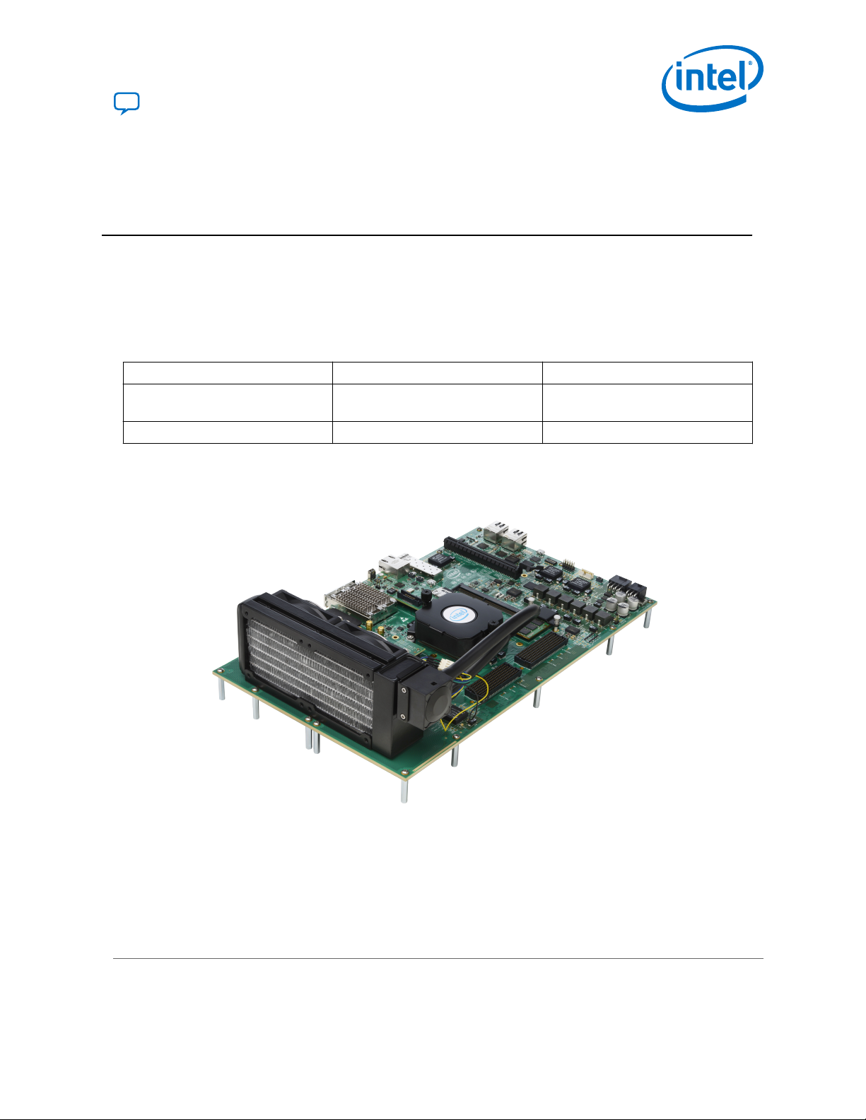
This development board comes in two different versions as shown in the table below.
Table 1. Development Kit Version Information
Development Kit Version Ordering Code Device Part Number
Intel Stratix 10 SX SoC L-Tile DK-SOC-1SSX-L-A
DK-SOC-1SSX-L-D
Intel Stratix 10 SX SoC H-Tile DK-SOC-1SSX-H-A 1SX280HU2F50E1VGAS
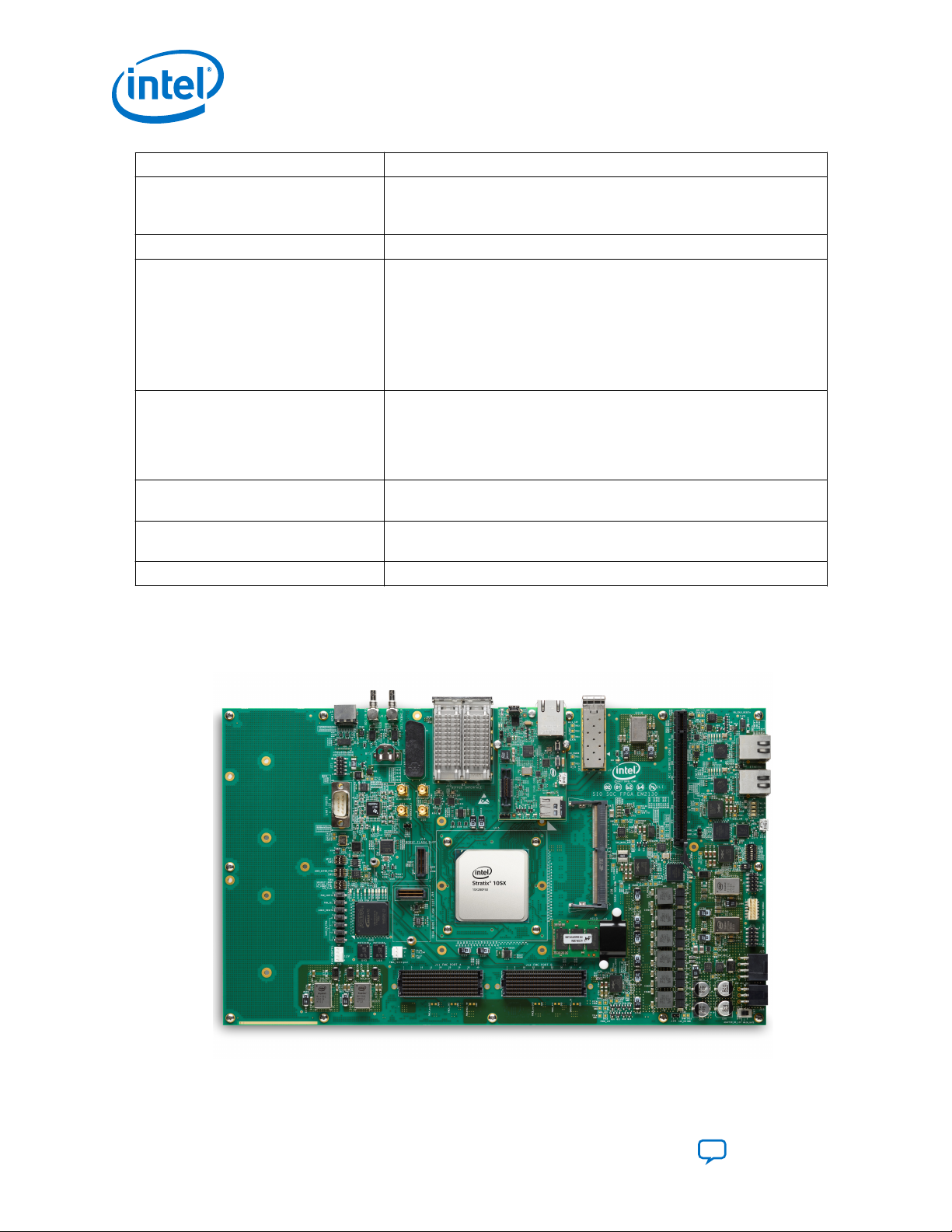
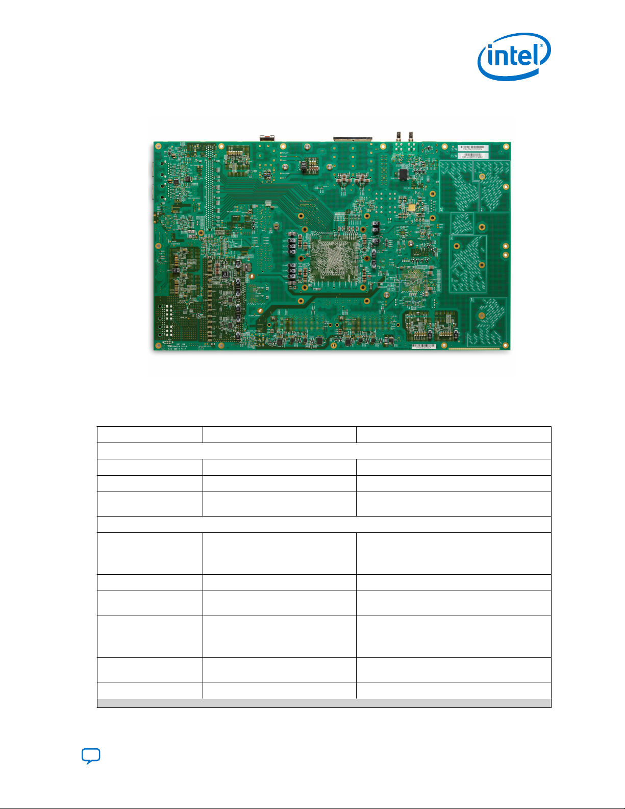
Figure 1. Development Kit Picture
1SX280LU2F50E1VG
1.1. General Development Kit Description
The Intel Stratix 10 SoC development board provides a hardware platform for
developing and prototyping low-power, high-performance and logic-intensive designs
using Intel Stratix 10 SoC. The board provides a wide range of peripherals and
memory interfaces to facilitate the development of Intel Stratix 10 SoC designs.
Intel Corporation. All rights reserved. Agilex, Altera, Arria, Cyclone, Enpirion, Intel, the Intel logo, MAX, Nios,
Quartus and Stratix words and logos are trademarks of Intel Corporation or its subsidiaries in the U.S. and/or
other countries. Intel warrants performance of its FPGA and semiconductor products to current specifications in
accordance with Intel's standard warranty, but reserves the right to make changes to any products and services
at any time without notice. Intel assumes no responsibility or liability arising out of the application or use of any
information, product, or service described herein except as expressly agreed to in writing by Intel. Intel
customers are advised to obtain the latest version of device specifications before relying on any published
information and before placing orders for products or services.
*Other names and brands may be claimed as the property of others.
ISO
9001:2015
Registered
Page 5
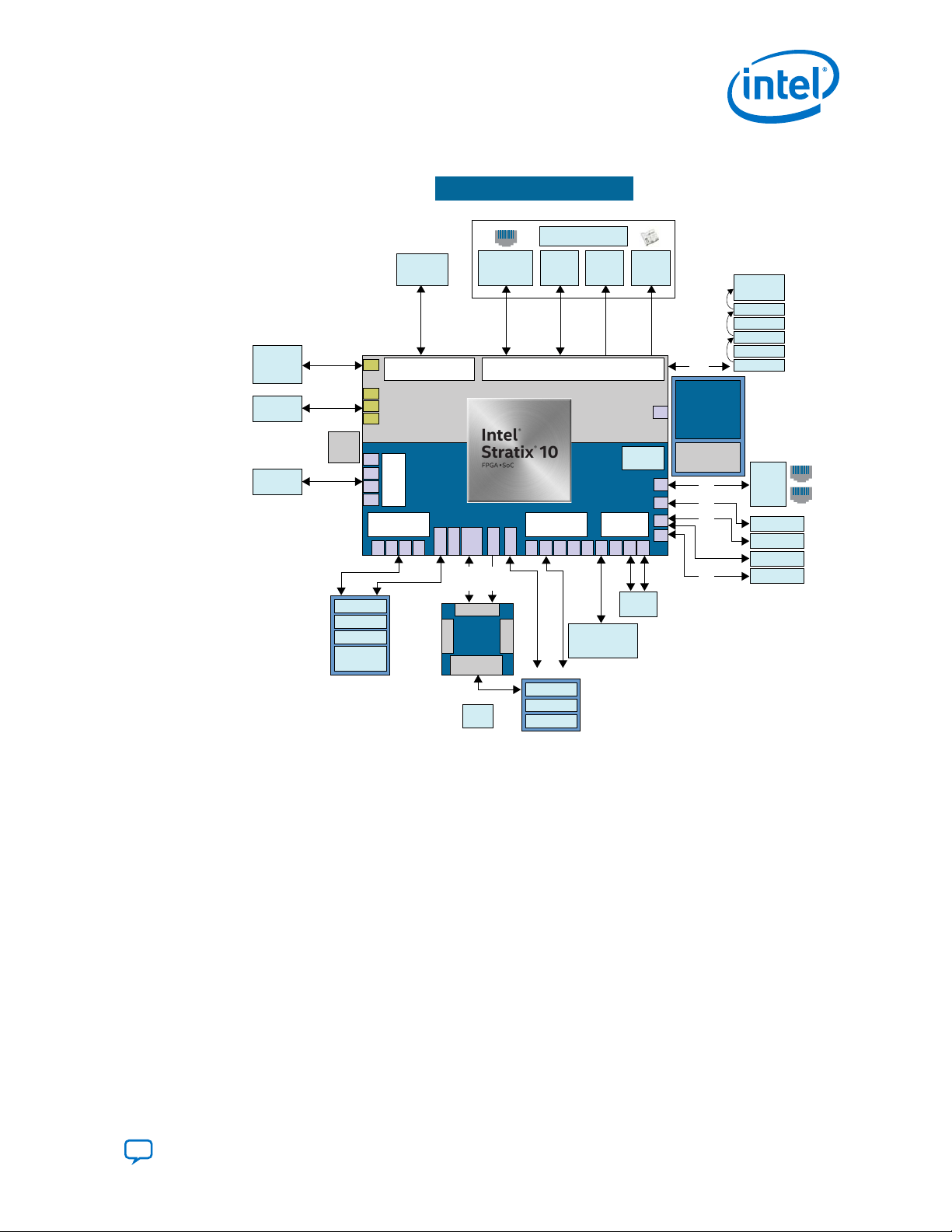
PCle® Gen3 x 16
Hardcore CxP
PCle® Gen3 x 16
Hardcore
100G / 50G
Hardcore
DDR3/DDR4
Hardcore
1C
24 Channels
DDR4 Dual
Rank
Clock
Block
DDR4
Signal Rank
HILO x72
FPGA Boot
Flash DC
(optional)
SODIMM x72
SDMI Bus
LVDS Bus
1D 1E 1F 1K 1L 1M 1N 4C 4D 4E 4F 4N
ZQSFP
x2
PCle
Gen3/Gen2/Gen1
x16 RC
FMCA
V57.4
PCle EP
Trace 16/32
(optional)
68-Bit Bus
24 Channels
16 Channels
FMCA
V57.4
PCle EP
FPGA_I/O
HBA, HBB
FPP
Flash
Intel
MAX 10
FPGA
Avalon-ST
Intel MAX 10
FPGA_I/O
DPIO
SDI_I/O
2F
SDM + JTAG + 05Cdk1 HPS_I/O
HPS
3A
FPGA
SGMII
MAC CORE
2M
2M
2L
3I
3J
3K
3L
2A
/
2B
3C
/
3B
3A
/
3L
FPGA
I/O
2C
/
2B
4E
MXP
SEEPROM/
RTC/TEMP
ClockI2C
PMBUS_VID
Ext I2C 1
Ext I2C 2
I2C 1
HPS Daughtercard
USB 2.0
PHY
USB3320
10/100/1000
RGMII PHY
KSZ9031RNX
UART
to USB
Boot Flash
DC
SDMI Bus
RGMII
USB2.0
UART1 TX/RX
Micro
SD Port
LT_12C
SFP+
HDMI
SDI/Ox1
x1
x4
x2
Intel® MAX 10
FPGA
JTAG Switch
and Power
Sequencer
Controller
Intel FPGA
Download
Cable II
2X
SGMII
PHY
88E1111
4 Channels
4L
4K
4M
Avalon®-ST
16/32 Bus
Intel® Enpirion® Power Solutions
1. Overview
UG-20081 | 2020.09.08
Figure 2. Intel Stratix 10 SoC Development Kit Block Diagram
Intel® Stratix® 10 SX SoC Development Kit User Guide
1.2. Recommended Operating Conditions
• Recommended ambient operating temperature range: 0 °C to 45 °C
1.3. Handling the Development Kit
Caution: Without proper anti-static handling, the board can be damaged. Therefore, use anti-
Caution: You must not operate this development kit in a vibration environment.
Send Feedback
• Maximum ICC load current: 190 A
• Maximum ICC load transient percentage: 30%
• FPGA maximum power supported by the supplied heatsink/fan: 300 W
When handling the board, it is important to observe static discharge precautions.
static handling precautions when touching the board.
5
Page 6

UG-20081 | 2020.09.08
Send Feedback
2. Getting Started
2.1. Installing Quartus Prime Software
The Intel Quartus® Prime design software is a multiplatform design environment that
easily adapts to your specific needs in all phases of FPGA, CPLD, and SoC designs. The
Intel Quartus Prime software delivers the highest performance and productivity for
Intel FPGAs, CPLDs, and SoCs.
Design software must enable dramatically increased design productivity in order to
take advantage of devices with multi-million logic elements with increased capabilities
that provide designers with an ideal platform to meet next-generation design
opportunities.
The new Intel Quartus Prime Design Suite design software includes everything needed
to design for Intel FPGAs, SoCs and CPLDs from design entry and synthesis to
optimization, verification and simulation. The Intel Quartus Prime Design Suite
software includes an additional Spectra-Q® engine that is optimized for Intel Stratix
10 and future devices. The Spectra-Q engine enables new levels of design productivity
for next generation programmable devices with a set of faster and more scalable
algorithms, a hierarchical database infrastructure and a unified compiler technology.
Intel Quartus Prime
The Intel Quartus Prime Design Suite software is available in three editions based on
specific design requirements: Pro, Standard, and Lite Edition.
The Intel Quartus Prime Pro Edition is optimized to support the advanced features in
Intel's next generation FPGAs and SoCs and requires a paid license.
Intel Quartus Prime Standard Edition includes the most extensive support for Altera's
latest device families and requires paid license.
Intel Quartus Prime Lite Edition provides an ideal entry point to Intel's high-volume
device families and is available as a free download with no license file required.
Included in the Intel Quartus Prime Pro Edition are the Intel Quartus Prime software,
Nios® II EDS and the MegaCore IP Library.
To install Intel's development tools, download the Intel Quartus Prime Pro Edition
software from the Quartus Prime Pro Edition page in the Download Center of Intel's
website.
Intel Corporation. All rights reserved. Agilex, Altera, Arria, Cyclone, Enpirion, Intel, the Intel logo, MAX, Nios,
Quartus and Stratix words and logos are trademarks of Intel Corporation or its subsidiaries in the U.S. and/or
other countries. Intel warrants performance of its FPGA and semiconductor products to current specifications in
accordance with Intel's standard warranty, but reserves the right to make changes to any products and services
at any time without notice. Intel assumes no responsibility or liability arising out of the application or use of any
information, product, or service described herein except as expressly agreed to in writing by Intel. Intel
customers are advised to obtain the latest version of device specifications before relying on any published
information and before placing orders for products or services.
*Other names and brands may be claimed as the property of others.
ISO
9001:2015
Registered
Page 7

2. Getting Started
UG-20081 | 2020.09.08
2.2. Installing the Intel FPGA Download Cable
The Intel Stratix 10 SoC Development Kit includes embedded Intel FPGA Download
Cable circuits for FPGA and Intel MAX® 10 programming. However, for the host
computer and board to communicate, you must install the Intel FPGA Download Cable
driver on the host computer.
Installation instructions for the Intel FPGA Download Cable driver for your operating
system are available on the Intel website.
On the Intel website, navigate to the Cable and Adapter Drivers Information link to
locate the table entry for your configuration and click the link to access the
instructions.
2.3. Installing the Intel SoC Embedded Development Suite (EDS)
The Intel SoC EDS is a comprehensive software tool suite for embedded software
development on Intel SoC devices. It contains development tools, utility programs,
run-time software, and application examples to expedite firmware and application
software of SoC embedded systems.
As a part of the Intel SoC EDS, the Arm* Development Studio (DS) Intel SoC FPGA
Edition Toolkit provides a comprehensive set of embedded development tools for
Intel's SoC FPGAs.
For more information and steps to install the SoC EDS Tool Suite refer to the links
below.
Related Information
• Arm Development Studio (DS) Intel SoC FPGA Edition
• Intel SoC FPGA Embedded Development Suite User Guide
2.4. Installing the Intel Stratix 10 SX SoC Development Kit Package
The Intel Stratix 10 SX SoC Development Kit offers a quick and simple approach for
developing custom Arm processor-based SoC designs. The Intel Stratix 10 SX SoCs
offer full software compatibility with previous generation SoCs, a broad ecosystem of
Arm software and tools, and the enhanced FPGA and digital signal processing (DSP)
hardware design flow.
Intel Stratix 10 SX SoC Development Kit Package Installer is a single installation file
contains that Intel Stratix 10 SX SoC Development Kit board design files, documents,
and examples including the Board Test System (BTS) installation files.
Download and unzip Intel Stratix 10 SX SoC Development Kit Package Installer first.
Install the Intel Stratix 10 SX SoC Board Test System.
Note:
To view the the layout *.brd files in the board package, you can download the
Cadence® Allegro®/OrCAD® Free Viewer from Cadence's website.
For additional information, refer to the Intel Stratix 10 SX SoC Development Kit
webpage on Intel's website using the link provided at the end of this section.
Send Feedback
Intel® Stratix® 10 SX SoC Development Kit User Guide
7
Page 8

Related Information
• Intel Stratix 10 SX SoC Development Kit
• Cadence Allegro
2. Getting Started
UG-20081 | 2020.09.08
Intel® Stratix® 10 SX SoC Development Kit User Guide
8
Send Feedback
Page 9
UG-20081 | 2020.09.08
Send Feedback
3. Development Kit Setup
The instructions in this chapter explain how to setup the Intel Stratix 10 SoC
Development Board.
3.1. Inspect the Development Kit
To inspect the board, perform the following steps:
1. Place the board on an anti-static surface and inspect it to ensure that it has not
been damaged during shipment.
2. Verify that all components on the board appear in place and intact.
Caution: Without proper anti-static handling, you could damage the board.
Table 2. Stratix 10 SoC Development Kit Contents
Item Quantity
Intel Stratix 10 SoC Development Board 1
USB Cable 2
USB Cable Micro 1
Ethernet Cable 1
HPS IO48 OOBE Daughter Card 1
HPS IO48 NAND Daughter Card 1
SODIMM Memory Card 1
QSPI Flash 1
SD Micro Flash 1
Related Information
• Thermal Management for FPGAs
• Intel Intel Enpirion® Digital Power Configurator Graphical User Interface (GUI)
3.2. Default Setup of the Development Kit
This development kit ships with its board switches preconfigured to support the design
examples in the kit.
1. Power up the development board by using the included power supply.
2. When configuration is complete, the configuration done green LED (D22)
illuminates, signaling that the Intel Stratix 10 device is configured successfully.
Intel Corporation. All rights reserved. Agilex, Altera, Arria, Cyclone, Enpirion, Intel, the Intel logo, MAX, Nios,
Quartus and Stratix words and logos are trademarks of Intel Corporation or its subsidiaries in the U.S. and/or
other countries. Intel warrants performance of its FPGA and semiconductor products to current specifications in
accordance with Intel's standard warranty, but reserves the right to make changes to any products and services
at any time without notice. Intel assumes no responsibility or liability arising out of the application or use of any
information, product, or service described herein except as expressly agreed to in writing by Intel. Intel
customers are advised to obtain the latest version of device specifications before relying on any published
information and before placing orders for products or services.
*Other names and brands may be claimed as the property of others.
ISO
9001:2015
Registered
Page 10
3. Development Kit Setup
UG-20081 | 2020.09.08
Caution: Use only the provided power supply. Power regulation circuits on the board can be
damaged by power supplies with greater voltage and a lower-rated power supply may
not be able to provide enough power for the board.
Table 3. Default Setup
Checkpoint Name Reference Description
1 Power Switch SW7 Power is turn off at left position
2 Power Adapter connector J25, J55 Both connectors can be used to connect the
3 Intel Intel Enpirion
4 JTAG Dongle connector J1 You can install Intel JTAG dongle to access
5 JTAG Switch SW1 Default Setup from bit 1 to bit 8 is “off, off,
6 USB JTAG Port J57 You need connect Micro USB cable to access
7 12V Fan Connector J16 You need use it to connect thermal Fan
8 Boot Switch SW4 Default set up from bit 1 to Bit 4 is “on, off,
9 MSEL Switch SW2 Default Setup is “on on on on”: JTAG mode
®
J29 You can install Intel Enpirion dongle to
power adapter
monitor the board power rails. Switch 8 is at
off position.
FPGA
on, on, on, on, on, on”: Intel Stratix 10 SoC
and Intel MAX 10 are on the JTAG chain
Intel Stratix 10 SoC
on, off”
FPGA/HPS I2C is enabled. Daughter card
power is on
3.3. Intel MAX 10 System Controller Updates
The Intel MAX 10 System Controller manages several features on the Intel Stratix 10
SX SoC Development kit, including clocks, I2C, and some configuration signals. In
certain situations, it may be necessary to ensure the Intel MAX 10 System Controller
internal flash contains the latest available design. This may include the Intel Stratix 10
device failing to configure from OSC_CLK_1, or when other unexpected issues arise.
The latest System Controller design is included in the Intel Stratix 10 SX Soc
Development Kit Installer Package, in the “system_max10” folder inside the
“examples” folder.
To update the internal flash, follow the steps outlined in the procedure below:
1. Power off the Intel Stratix 10 SX SoC Development Kit.
2. Ensure SW1 and SW2 are set to the default settings so the System Intel MAX 10
is on the JTAG chain and the Intel Stratix 10 device does not automatically
configure itself.
3. Connect a micro USB cable to J57 for JTAG access and power on the board.
4. Open the Intel Quartus Prime Programmer and scan the device chain.
5. Right click on the Intel MAX 10 and select “Change File”. Navigate to the
“system_max10” folder and select the .pof file, for example,
“max10_system_rev13.pof”.
Intel® Stratix® 10 SX SoC Development Kit User Guide
10
Send Feedback
Page 11
3. Development Kit Setup
UG-20081 | 2020.09.08
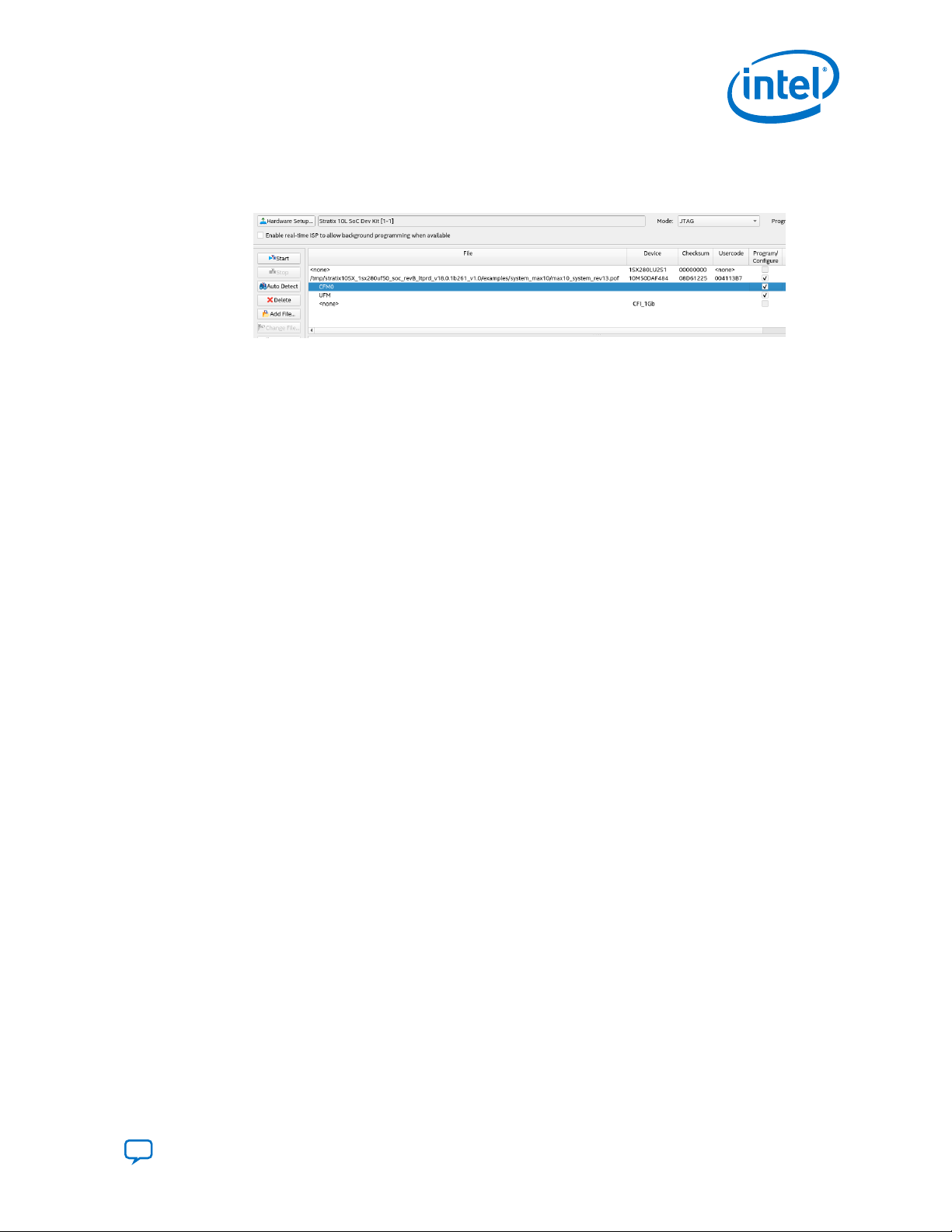
6.
Check the Program/Verify box in the row with the .pof and the Intel MAX 10
Device. The Program/Verify boxes in the immediately following rows, CFM0 and
UFM, will auto-check as well. Refer to the following screenshot:
7. Click Start and wait for the programming cycle to finish.
8. Power off the board and reset SW1 and SW2 to prior settings, if any.
Send Feedback
Intel® Stratix® 10 SX SoC Development Kit User Guide
11
Page 12
UG-20081 | 2020.09.08
Send Feedback
4. Development Kit Components
This chapter introduces the major components on the Intel Stratix 10 Development
Board. The board overview figure illustrates the component locations and the board
components table provides a brief description of all component features of the board.
4.1. Development Kit Feature Summary
Table 4. Intel Stratix 10 SoC Development Kit Feature Summary
Feature Description
Programmable Logic • Intel Stratix 10 SoC FPGA
• 10M04SCU169C8G Intel MAX 10 CPLD as the Intel FPGA Download Cable
and JTAG switch device
• 10M16SAU169C8G Intel MAX 10 CPLD as the Power manager and
sequencer device
• 10M50DAF484I7G Intel MAX 10 CPLD as the IO level translator, IO MUX
and Passive AVST-16 FPGA controller device
HPS memory 1066 MHz 4 GB 72-bit HILO memory card
HPS Boot Flash (Flash Card) • Boot Codes for QSPI, SD Micro
• QSPI Flash: 256 MB (MT25QU02GCBB8E12-0SIT)
• SD Micro Flash Card: 16 GB (Kingston)
HPS IO48 OOBE Daughter Card • One HPS IO48 60-pin Samtec Connector
• One RGMII 10/100/1000 Mbps Ethernet port: Standard RJ-45
• One UART port: Standard USB Mini-B Receptacle
• One Micro SD Card Connector: Standard Micro SD Card Socket
• One USB 2.0 port: Standard USB Micro-AB Receptacle
• One Mictor 38-pin connector (JTAG only without Trace signals)
— Two JTAG targets selected by the resistors MUX: FPGA JTAG chain
(optional) and HPS JTAG Port (default)
• I2C: HPS I2C port
• GPIO
— 2 Push buttons
— 3 LEDs
— 1 Ethernet Interrupt from Ethernet PHY
— 1 USB over-current indicator
• HPS Clock: 25 MHz oscillator
HPS IO48 NAND Flash Daughter Card • One HPS IO48 60-pin Samtec connector
• One RGMII 10/100/1000 Mbps Ethernet port: Standard RJ-45
• One UART port: Standard USB Mini-B Receptacle
• NAND Flash (x16): 8 Gb
• eMMC (x8): 8 GB 5.0 compliant eMMC
continued...
Intel Corporation. All rights reserved. Agilex, Altera, Arria, Cyclone, Enpirion, Intel, the Intel logo, MAX, Nios,
Quartus and Stratix words and logos are trademarks of Intel Corporation or its subsidiaries in the U.S. and/or
other countries. Intel warrants performance of its FPGA and semiconductor products to current specifications in
accordance with Intel's standard warranty, but reserves the right to make changes to any products and services
at any time without notice. Intel assumes no responsibility or liability arising out of the application or use of any
information, product, or service described herein except as expressly agreed to in writing by Intel. Intel
customers are advised to obtain the latest version of device specifications before relying on any published
information and before placing orders for products or services.
*Other names and brands may be claimed as the property of others.
ISO
9001:2015
Registered
Page 13
4. Development Kit Components
UG-20081 | 2020.09.08
Feature Description
• I2C: HPS I2C port
• GPIO
— 2 Push Buttons
— 3 LEDs
— 1 Ethernet Interrupt from Ethernet PHY
• HPS Clock: 25 MHz oscillator
FPGA memory 1200 MHz 16 GB DDR4 SO-DIMM MTA18ASF2G72HZ – 2G6
FPGA File Flash (Flash Card) • NAND Flash (x8): 1 GB
• QSPI Flash: 256 MB
• SD Micro Flash Card: 16 GB (Kingston)
Two V57.4 High Pin Count FMC+ Slots • 28 Gbps signals: Insertion loss less than 5 dB, return loss less than 10 dB
• FMC+ PCIe* Gen3 x16 cable (not included)
• FMC to PCIe Gen3 x8 cable (not included)
• 16/32 bit trace
Note: FMC to PCIe cables are sold separately by Samtec. Please contact
them directly regarding P/N HDR-201768-01-PCIEC
FPGA PCIe Gen 1/2/3 x16 RC Slot • 75 W Power
• Meets PCIe specifications
FPGA Communication Ports • Two 28 Gbps ZQSFP+ Ports: 100/50 Gbps IP, Insertion loss less than 5
FPGA Debug Ports Intel FPGA Download Cable Direct Port & JTAG
FPGA Reference Clocks • Clock Cleaner
I2C Devices • 4 KB SEEPROM
Intel MAX 10 Controller I/O CPLD Features • System Reset Controller
dB, return loass less than 10 dB
• One 10 Gbps SFP+ Port: 10 Gbps Ethernet IP
• SMA Test Port: Up to four 28 Gbps channels, inseertion loss less than 5
dB, return loss less than 10 dB, one external reference clock
• One DB-9 RS-232 Port (MAX3221)
— 122.88 MHz (Network)
— 644.5312 MHz (Network)
— 297 MHz (SDI)
— 245 MHz (SDI)
• Clock Generators
— LMH1983 (27 MHz, 148.5 MHz)
— Si5388 (133.33 MHz)
— PCIe (100 MHz)
— Si5338 (148 MHz, 100 MHz, 27 MHz, 100 MHz)
— Si5341 (155.52 MHz, 644.53125 MHz, 135 MHz, 156.25 MHz, 625
MHz, 100 MHz, 125 MHz, 125 MHz)
• Real Time Clock
• Silicon Labs™ Clock Generators
• FMC+ Slots
• PCIe Slots
• SFP+
• ZQSFP
• Clock Cleaner
• Power Supplies
• FPGA PS AVST Configuration Controller
• I2C Master Controller
continued...
Send Feedback
Intel® Stratix® 10 SX SoC Development Kit User Guide
13
Page 14
4. Development Kit Components
Feature Description
• UART Level Shifter
• FPGA I/O MUX
• SDI/HDMI/QSFP/SFP+ I/O level shift
Intel MAX 10 Power CPLD Sequencer FPGA, PCIe, FMC+ slots power sequencer, Reset.
Intel MAX 10 CPLD Features • Intel FPGA Download Cable II
• JTAG Switch
— Input JTAG Sources (Intel FPGA Download Cable II, 10-pin Program
Header, FMCA+, FMCB+, Mictor JTAG)
— Output JTAG Sources (Intel MAX 10 A JTAG, MAX10B JTAG, Intel
Stratix 10 JTAG, FMCA+, FMCB+, PCIe)
— JTAG Program
— User I/O
User I/O • 4 Push Buttons
• 4-bit Dipswitch
• 4 User LEDs
• 2-pin I/O Header
• System Intel MAX 10 LEDs and 4-bit switch
Power • Volgen KTPS200-12160, 12V, 24A
• ATX-Power
Mechanical • 8.5" x 14.5" Rectangular Form Factor
• Liquid cool thermal heat sink (300W @ 35C)
System Monitor Power, Voltage, Current
UG-20081 | 2020.09.08
4.2. Board Components
Figure 3. Board Picture (Top View)
Intel® Stratix® 10 SX SoC Development Kit User Guide
14
Send Feedback
Page 15
4. Development Kit Components
UG-20081 | 2020.09.08
Figure 4. Board Picture (Bottom View)
Board Components Table
Table 5. Intel Stratix 10 SoC Board Components Table
Board Reference Type Description
Featured Device
U15 FPGA Intel Stratix 10 SoC FPGA
U43 CPLD Intel MAX 10 10M50DAF484I7G System Controller
U46 CPLD Intel MAX 10 10M16SAU169C8G Power Manager
Configuration, Status and Setup Elements
J1 JTAG chain header Provides access to the JTAG chain and disables the
SW1 JTAG chain control DIP switch Remove or include devices in the active JTAG chain
SW2 MSEL DIP Switch Controls the configuration scheme on the board.
J57 Micro-USB Header USB interface to on-board Intel FPGA Download
SW4 Function DIP Switch Selects I2C master, controls PCIe slot power and
SW8 Power Switch ON position: Power GUI
CPLD
on-board Intel FPGA Download Cable II when using
an external JTAG debugger such as an Intel FPGA
Download Cable II
MSEL pin 0,1,2 connect to the DIP Switch
Cable II JTAG for programming and debugging
HPS, FPGA orIntel MAX 10 CPLD through a type-B
Micro-USB cable.
selects FPGA image source
continued...
Send Feedback
Intel® Stratix® 10 SX SoC Development Kit User Guide
15
Page 16
4. Development Kit Components
UG-20081 | 2020.09.08
Board Reference Type Description
OFF position: Intel Enpirion dongle
S2 Program select push button Toggles the program select LEDs which selects the
S1 Configure push button Load image from flash memory to the FPGA based
D22 Configuration done LED Illuminates when the FPGA is configured
D20 Load LED Illuminates when the Intel MAX 10 CPLD System
D19 Error LED Illuminates when the FPGA configuration from flash
D31 Power LED Illuminates when 3.3V power is present
D1, D2 JTAG TX/RX LEDs Indicates the transmit or receive activity of the
D24, D26, D28 Program select LEDs Illuminates to show which flash memory image
D29, D30 FMC port present LEDs Illuminates when a daughtercard is plugged into
Clock Circuits
U26 Multi-output oscillator Si5338A quad-output fixed oscillator with 148.5
U29 50-MHz oscillator 50 MHz crystal oscillator for general purpose logic
U25 Multi-output oscillator Two 100 MHz outputs for PCIe application
J19, J20 Clock input SMA connector External clock inputs for the transceiver test port
U33 Multi-output oscillator Si5341 ten-output fixed oscillator
U31 Multi-output oscillator Si5338A quad-output fixed oscillator with four
U34 Multi-output clock cleaner LMK05028 Clock Cleaner
General User Input/Output
D21, D23, D25, D27 User LEDs Four user LEDs. Illuminate when driven high.
SW3 User DIP Switch User DIP switch. When the switch is ON, a logic 0
S3 FPGA Reset Push Button Reset the FPGA logic
S4, S5, S6, S7 General user push buttons Four user push buttons. Driven low when pressed
S20 HPS Reset Push Buttons HPS cold/warm reset push buttons
Memory Connectors
J134 HPS HILO Memory Connector HPS memory card include DDR3 HILO memory
J14 Boot Flash Connector Boot flash card options include QSPI flash card, SD
program image that loads from flash memory to
the FPGA
on the settings of the program select LEDs
Controller
memory fails
JTAG chain. The TX and RX LEDs flicker if the link
is in use and active. The LEDs are either off when
not in use or on when in use but idle
loads to the FPGA when you press the program
select push button
the FMC port
MHz, 100 MHz, 27 MHz and 100 MHz outputs
133.33 MHz outputs
is selected
card and DDR4 HILO memory card
micro flash card
continued...
Intel® Stratix® 10 SX SoC Development Kit User Guide
16
Send Feedback
Page 17
4. Development Kit Components
UG-20081 | 2020.09.08
Board Reference Type Description
J28 SO-DIMM 16 GB SO-DIMM DDR4 Memory Card
U41 I2C EEPROM 32 Kb I2C serial EEPROM
Communication Ports
J53 PCIe socket Gen3 x16 Socket
J11, J12 FMC Port J29 is a V57.4 compatible FMC connector. J19 is a
J7 SFP+ Port One SFP+ Ports
J3 Gigabit Ethernet Port SGMII Gigabit Ethernet port through FPGA
J4 Gigabit Ethernet Port SGMII Gigabit Ethernet Port through FPGA
J9-J10 QSFP28 Optical Transceiver Interface 17 Gbps/28 Gbps, 8 channels connected to QSFP28
J57, U2 USB-UART Port Mini-B USB interface to USB-to-UART bridge for
J22 DB9 UART Port DB9 RS-232 UART Port
U42 Real-time clock DS1339 device with built-in power sense circuit
Video and Display Ports
J8 HDMI Port Display Port interface
J5, U13 SDI Video Output Port HDBNC 75-Ohm SDI video TX interface
J6, U14 SDI Video Input Port HDBNC 75-Ohm SDI video RX interface
J29 Power GUI Connector Intel Enpirion Power GUI Connector
Power Supply
J25, J55 DC input jack Accepts 12 V DC power supply
SW7 Power Switch Switch to power on or off the board when power is
FMC connector defined by Intel 16 transceivers
specification
transceiver
transciever
modules
serial UART interface
that detects power failures and automatically
switches to backup battery supply, maintaining
time keeping even when the board is not powered
supplied from the DC input jack
4.3. Intel Stratix 10 SoC Device Overview
Intel's 14-nm Intel Stratix 10 SX SoCs deliver 2x core performance and up to 70%
lower power over previous generation high-performance SoCs. Featuring several
groundbreaking innovations, including the all new Intel Hyperflex™ core architecture,
this device family enables you to meet the demand for ever-increasing bandwidth and
processing performance in you most advanced applications, while meeting your power
budget.
Featuring several groundbreaking innovations, including the all new HyperFlex™ core
architecture, this device family enables you to meet the demand for ever-increasing
bandwidth and processing performance in your most advanced applications, while
meeting your power budget.
Send Feedback
Intel® Stratix® 10 SX SoC Development Kit User Guide
17
Page 18

4. Development Kit Components
UG-20081 | 2020.09.08
With an embedded hard processor system (HPS) based on a quad-core 64-bit Arm
Cortex*-A53, the Stratix 10 SoC devices deliver power efficient, application-class
processing and allow designers to extend hardware virtualization into the FPGA fabric.
Stratix 10 SoC devices demonstrate Intel's commitment to high-performance SoCs
and extend Intel's leadership in programmable devices featuring an Arm-based
processor system.
Important innovations in Stratix 10 FPGAs and SoCs include:
• All new HyperFlex core architecture delivering 2X the core performance compared
to previous generation high-performance FPGAs
• Industry leading Intel 14-nm Tri-Gate (FinFET) technology
• Heterogeneous 3D System-in-Package (SiP) technology
• Monolithic core fabric with up to 5.5 million logic elements (LEs)
• Up to 96 full duplex transceiver channels on heterogeneous 3D SiP transceiver
tiles
• Transceiver data rates up to 28.3 Gbps chip-to-chip/module and backplane
performance
• Embedded eSRAM (45 Mbit) and M20K (20 kbit) internal SRAM memory blocks
• Fractional synthesis and ultra-low jitter LC tank based transmit phase locked loops
(PLLs)
• Hard PCI Express® Gen3 x16 intellectual property (IP) blocks
• Hard 10GBASE-KR/40GBASE-KR4 Forward Error Correction (FEC) in every
transceiver channel
• Hard memory controllers and PHY supporting DDR4 rates up to 2666 Mbps per pin
• Hard fixed-point and IEEE 754 compliant hard floating-point variable precision
digital signal processing (DSP) blocks with up to 10 TFLOPS compute performance
with a power efficiency of 80 GFLOPS per Watt
• Quad-core 64-bit Arm Cortex-A53 embedded processor running up to 1.5 GHz in
SoC family variants
• Programmable clock tree synthesis for flexible, low power, low skew clock trees
• Dedicated secure device manager (SDM) for:
— Enhanced device configuration and security
— AES-256, SHA-256/384 and ECDSA-256/384 encrypt/decrypt accelerators and
authentication
— Multi-factor authentication
— Physically Unclonable Function (PUF) service and software programmable
device configuration capability
• Comprehensive set of advanced power saving features delivering up to 70% lower
power compared to previous generation high-performance FPGAs
• Non-destructive register state readback and writeback, to support ASIC
prototyping and other applications
Intel® Stratix® 10 SX SoC Development Kit User Guide
18
Send Feedback
Page 19
4. Development Kit Components
UG-20081 | 2020.09.08
With these capabilities, Stratix 10 FPGAs and SoCs are ideally suited for the most
demanding applications in diverse markets such as:
• Compute and Storage—for custom servers, cloud computing and data center
acceleration
• Networking—for Terabit, 400G and multi-100G bridging, aggregation, packet
processing and traffic management
• Optical Transport Networks—for OTU4, 2xOTU4, 4xOTU4
• Broadcast—for high-end studio distribution, headend encoding/decoding, edge
quadrature amplitude modulation (QAM)
• Military—for radar, electronic warfare, and secure communications
• Medical—for diagnostic scanners and diagnostic imaging
• Test and Measurement—for protocol and application testers
• Wireless—for next-generation 5G networks
• ASIC Prototyping—for designs that require the largest monolithic FPGA fabric
with the highest I/O count
Intel Stratix 10 SX SoC devices have a feature set that is identical to the Intel Stratix
10 FPGA devices, with the addition of an embedded quad-core 64-bit Arm Cortex A53
Hard Processor System.
Common to all Stratix 10 family variants is a high-performance fabric based on the
new HyperFlex core architecture that includes additional Hyper-Registers throughout
the interconnect routing and at the inputs of all functional blocks. The core fabric also
contains an enhanced logic array utilizing Intel’s adaptive logic module (ALM) and a
rich set of high performance building blocks including:
To clock these building blocks, Stratix 10 devices use programmable clock tree
synthesis, which uses dedicated clock tree routing to synthesize only those branches
of the clock trees required for the application. All devices support in-system, finegrained partial reconfiguration of the logic array, allowing logic to be added and
subtracted from the system while it is operating.
All family variants also contain high speed serial transceivers, containing both the
physical medium attachment (PMA) and the physical coding sublayer (PCS), which can
be used to implement a variety of industry standard and proprietary protocols. In
addition to the hard PCS, Stratix 10 devices contain multiple instantiations of PCI
Express hard IP that supports Gen1/Gen2/Gen3 rates in x1/x2/x4/x8/x16 lane
configurations, and hard 10GBASE-KR/40GBASE-KR4 FEC for every transceiver. The
hard PCS, FEC, and PCI Express IP free up valuable core logic resources, save power,
and increase your productivity.
Table 6. Stratix 10 FPGA and SoC Common Device Features
Feature Description
Technology • 14-nm Intel Tri-Gate (FinFET) process technology
• SmartVoltage ID (VID) controlled standard VCC option
• 0.8 V and 0.85 V optional VCC core voltage
Low power serial
transceivers
• Up to 96 total transceivers available
• Continuous operating range of 1 Gbps to 28.3 Gbps for Stratix 10 GX/SX devices
• Backplane support up to 28.3 Gbps for Stratix 10 GX/SX devices
continued...
Send Feedback
Intel® Stratix® 10 SX SoC Development Kit User Guide
19
Page 20
4. Development Kit Components
UG-20081 | 2020.09.08
Feature Description
• Extended range down to 125 Mbps with oversampling
• ATX transmit PLLs with user-configurable fractional synthesis capability
• XFP, SFP+, QSFP/QSFP28, CFP/CFP2/CFP4 optical module support
• Adaptive linear and decision feedback equalization
• Transmit pre-emphasis and de-emphasis
• Dynamic partial reconfiguration of individual transceiver channels
• On-chip instrumentation (EyeQ non-intrusive data eye monitoring)
General purpose I/Os • Up to 1640 total GPIO available
• 1.6 Gbps LVDS—every pair can be configured as an input or output
• 1333 MHz/2666 Mbps DDR4 external memory interface
• 1067 MHz/2133 Mbps DDR3 external memory interface
• 1.2 V to 3.0 V single-ended LVCMOS/LVTTL interfacing
• On-chip termination (OCT)
Embedded hard IP • PCIe Gen1/Gen2/Gen3 complete protocol stack, x1/x2/x4/x8/x16 end point and root
Transceiver hard IP • 10GBASE-KR/40GBASE-KR4 Forward Error Correction (FEC)
Power management • SmartVoltage ID controlled standard VCC option
High performance monolithic
core fabric
Internal memory blocks • eSRAM - 45-Mbit with hard ECC support
Variable precision DSP
blocks
port
• DDR4/DDR3/LPDDR3 hard memory controller (RLDRAM3/QDR II+/QDR IV using soft
memory controller)
• Multiple hard IP instantiations in each device
• Single Root I/O Virtualization (SR-IOV)
• 10G Ethernet PCS
• PCI Express PIPE interface
• Interlaken PCS
• Gigabit Ethernet PCS
• Deterministic latency support for Common Public Radio Interface (CPRI) PCS
• Fast lock-time support for Gigabit Passive Optical Networking (GPON) PCS
• 8B/10B, 64B/66B, 64B/67B encoders and decoders
• Custom mode support for proprietary protocols
• Low static power device options
• Intel Quartus Prime Pro Edition integrated power analysis
• HyperFlex core architecture with Hyper-Registers throughout the interconnect routing
and at the inputs of all functional blocks
• Monolithic fabric minimizes compile times and increases logic utilization
• Enhanced adaptive logic module (ALM)
• Improved multi-track routing architecture reduces congestion and improves compile
times
• Hierarchical core clocking architecture with programmable clock tree synthesis
• Fine-grained partial reconfiguration
• M20K—20-Kbit with hard ECC support
• MLAB—640-bit distributed LUTRAM
• IEEE 754-compliant hard single-precision floating point capability
• Supports signal processing with precision ranging from 18x19 up to 54x54
• Native 27x27 and 18x19 multiply modes
• 64-bit accumulator and cascade for systolic FIRs
• Internal coefficient memory banks
• Pre-adder/subtractor improves efficiency
• Additional pipeline register increases performance and reduces power
continued...
Intel® Stratix® 10 SX SoC Development Kit User Guide
20
Send Feedback
Page 21
4. Development Kit Components
UG-20081 | 2020.09.08
Feature Description
Phase locked loops (PLL) • Fractional synthesis PLLs (fPLL) support both fractional and integer modes
• Fractional mode with third-order delta-sigma modulation
• Precision frequency synthesis
• Integer PLLs adjacent to general purpose I/Os, support external memory, and LVDS
interfaces, clock delay compensation, zero delay buffering
Core clock networks • 1 GHz fabric clocking
• 667 MHz external memory interface clocking, supports 2666 Mbps DDR4 interface
• 800 MHz LVDS interface clocking, supports 1600 Mbps LVDS interface
• Programmable clock tree synthesis, backwards compatible with global, regional and
peripheral clock networks
• Clocks only synthesized where needed, to minimize dynamic power
Configuration • Dedicated Secure Device Manager
• Software programmable device configuration
• Serial and parallel flash interface
• Configuration via protocol (CvP) using PCI Express Gen1/Gen2/Gen3
• Fine-grained partial reconfiguration of core fabric
• Dynamic reconfiguration of transceivers and PLLs
• Comprehensive set of security features including AES-256, SHA-256/384, and
ECDSA-256/384 accelerators, and multi-factor authentication
• Physically Unclonable Function (PUF) service
Packaging • Intel Embedded Multi-die Interconnect Bridge (EMIB) packaging technology
• Multiple devices with identical package footprints allows seamless migration across
different device densities
• 1.0 mm ball-pitch FBGA packaging
• Lead and lead-free package options
Software and tools • Intel Quartus Prime Pro Edition design suite with new Spectra-Q engine and Hyper-
Aware design flow
• Fast Forward compiler to allow HyperFlex architecture performance exploration
• Transceiver toolkit
• Qsys system integration tool
• DSP Builder advanced blockset
• OpenCL™ support
• SoC Embedded Design Suite (EDS)
Table 7. Stratix 10 SoC Specific Device Features
SoC Subsystem Feature Description
Hard Processor
System
Send Feedback
Multi-processor unit (MPU) core • Quad-core Arm Cortex-A53 MPCore processor with Arm
CoreSight debug and trace technology
• Scalar floating-point unit supporting single and double
precision
• Arm NEON media processing engine for each processor
System Controllers • System Memory Management Unit (SMMU)
• Cache Coherency Unit (CCU)
Layer 1 Cache • 32 KB L1 instruction cache with parity
• 32 KB L1 data cache with ECC
Layer 2 Cache • 1 MB Shared L2 Cache with ECC
On-Chip Memory • 256 KB On-Chip RAM
Direct memory access (DMA) controller • 8-Channel DMA
Intel® Stratix® 10 SX SoC Development Kit User Guide
continued...
21
Page 22
4. Development Kit Components
SoC Subsystem Feature Description
Secure Device
Manager
External
Memory
Interface
Ethernet media access controller
(EMAC)
USB On-The-Go controller (OTG) • 2 USB OTG with integrated DMA
UART controller • 2 UART 16550 compatible
Serial Peripheral Interface (SPI)
controller
I2C controller • 5 I2C controllers
SD/SDIO/MMC controller • 1 eMMC version 4.5 with DMA and CE-ATA support
NAND flash controller • 1 ONFI 1.0, 8- and 16-bit support
General-purpose I/O (GPIO) • Maximum of 48 software programmable GPIO
Timers • 4 general-purpose timers
Security • Secure boot
External Memory Interface • Hard Memory Controller with DDR4 and DDR3, and
• Three 10/100/1000 EMAC with integrated DMA
• 4 SPI
• SD, including eSD, version 3.0
• SDIO, including eSDIO, verion 3.0
• CE-ATA - version 1.1
• 4 watchdog timers
• Advanced Encryption Standard (AES) and authentication
(SHA/ECDSA)
LPDDR3
UG-20081 | 2020.09.08
For further information , please refer to the Intel Stratix 10 GX/SX Device Overview
available on the Intel website.
Related Information
Stratix 10 GX/SX Device Overview
4.4. Intel MAX 10 System Controller Overview
Intel MAX 10 devices are single-chip, non-volatile low-cost programmable logic devices
(PLDs) to integrate the optimal set of system components.
Intel MAX 10 devices are the ideal solution for system management, I/O expansion,
communication control planes, industrial, automotive, and consumer applications.
The highlights of the Intel MAX 10 devices include:
• Internally stored dual configuration flash
• User flash memory
• Instant on support
• Integrated analog-to-digital converters (ADCs)
• Single-chip Nios II soft core processor support
Intel® Stratix® 10 SX SoC Development Kit User Guide
22
Send Feedback
Page 23
4. Development Kit Components
UG-20081 | 2020.09.08
Table 8. Summary of Features for Intel MAX 10 Devices
Feature Description
Technology 55 nm TSMC Embedded Flash (Flash + SRAM) process technology
Packaging • Low cost, small form factor packages—support multiple packaging
Core architecture • 4-input look-up table (LUT) and single register logic element (LE)
Internal memory blocks • M9K—9 kilobits (Kb) memory blocks
User flash memory (UFM) • User accessible non-volatile storage
Embedded multiplier blocks • One 18 × 18 or two 9 × 9 multiplier modes
ADC • 12-bit successive approximation register (SAR) type
Clock networks • Global clocks support
Internal oscillator Built-in internal ring oscillator
PLLs • Analog-based
General-purpose I/Os (GPIOs) • Multiple I/O standards support
External memory interface (EMIF)
(1)
technologies and pin pitches
• Multiple device densities with compatible package footprints for seamless
migration between different device densities
• RoHS6-compliant
• LEs arranged in logic array block (LAB)
• Embedded RAM and user flash memory
• Clocks and PLLs
• Embedded multiplier blocks
• General purpose I/Os
• Cascadable blocks to create RAM, dual port, and FIFO functions
• High speed operating frequency
• Large memory size
• High data retention
• Multiple interface option
• Cascadable blocks enabling creation of filters, arithmetic functions, and image
processing pipelines
• Up to 17 analog inputs
• Cumulative speed up to 1 million samples per second ( MSPS)
• Integrated temperature sensing capability
• High speed frequency in clock network
• Low jitter
• High precision clock synthesis
• Clock delay compensation
• Zero delay buffering
• Multiple output taps
• On-chip termination (OCT)
• Up to 830 megabits per second (Mbps) LVDS receiver, 800 Mbps LVDS
transmitter
Supports up to 600 Mbps external memory interfaces:
• DDR3, DDR3L, DDR2, LPDDR2 (on 10M16, 10M25, 10M40 and 10M50)
• SRAM (Hardware support only)
continued...
(1)
EMIF is only supported in selected MAX 10 device density and package combinations. Refer to
the External Memory Interface User Guide for more information.
Send Feedback
Intel® Stratix® 10 SX SoC Development Kit User Guide
23
Page 24
Feature Description
Note: For 600 Mbps performance, –6 device speed grade is required.
Performance varies according to device grade (commercial, industrial, or
automotive) and device speed grade (–6 or –7). Refer to the MAX 10
Device Data Sheet or External Memory Interface Spec Estimator for more
details.
Configuration • Internal configuration
• JTAG
• Advanced Encryption Standard (AES) 128-bit encryption and compression
options
• Flash memory data retention of 20 years at 85 °C
Flexible power supply schemes • Single- and dual-supply device options
• Dynamically controlled input buffer power down
• Sleep mode for dynamic power reduction
4.5. FPGA Configuration
This development kit supports the following FPGA configurations:
• QSPI Configuration
• SDMMC x4 Configuration
• JTAG Only
4. Development Kit Components
UG-20081 | 2020.09.08
A 4-bit DIP Switch (SW2) is used to select the FPGA configuration mode.
Table 9. DIP Switch Bits
Switch Bit Name
1 MSEL0
2 MSEL1
3 MSEL2
4 Not Used
Table 10. DIP Switch Bit Description
MSEL2 MSEL1 MSEL0 Mode
OFF OFF ON QSPI
ON OFF OFF SDMMC x4, SDMMC x8
ON ON ON JTAG
Note: The default setting is JTAG mode. The default bit position is "ON, ON, ON, ON"
4.6. General User Input/Output
Table 11. User I/O Pin Map
Pin Name Schematic Signal Name Description
PIN_A24
PIN_B24
USER_LED_FPGA0
USER_LED_FPGA2
USER_LED0
USER_LED1
continued...
Intel® Stratix® 10 SX SoC Development Kit User Guide
24
Send Feedback
Page 25
4. Development Kit Components
UG-20081 | 2020.09.08
Pin Name Schematic Signal Name Description
PIN_F22
PIN_E22
PIN_A26
PIN_A25
PIN_D23
PIN_D24
PIN_B23
PIN_C23
PIN_E23
PIN_E24
USER_LED_FPGA1
USER_LED_FPGA3
USER_PB_FPGA0
USER_PB_FPGA1
USER_PB_FPGA2
USER_PB_FPGA3
USER_DIPSW_FPGA0
USER_DIPSW_FPGA1
USER_DIPSW_FPGA2
USER_DIPSW_FPGA3
4.7. Connectors and Interfaces
The FPGA portion of this development kit includes 96 transceivers.
Table 12. Channel Assignment for Transceiver Applications
USER_LED2
USER_LED3
USER_PB0
USER_PB1
USER_PB2
USER_PB3
USER_DPSW0
USER_DPSW1
USER_DPSW2
USER_DPSW3
Applications Channel (Bank, Number)
FMC+ A 1C (1C, 0-5), 1D (1D, 0-5), 1E (1E, 0-3), 1F (PCIE EP x16)
SFP+ Port (4C, 0)
PCIE RC x16 (4K, 0-5), (4L, 0-5), (4M, 0-3)
SGMII Port 1 and Port 2 (4M, 4), (4M, 5)
FMC+ B 1K (1K, 0-5), 1L (1L, 0-5), 1M (1M, 0-3), 1N (PCIE EPx16)
MXP Test Ports (4D, 0, 1, 3, 4)
SDI Port TX (4E,1), RX (4F, 0)
HDMI (4C, 2-5)
ZQSFP+ B (4F, (0,1,3,4))
ZQSFP+ A (4N, (0,1,3,4))
4.7.1. PCIe Slot
The PCIe root port is a PCIe Gen3 x16 port. This port is assigned to 4K, 4L and 4M
Banks. The transceiver I/O bank power is connected to 1.8 V.
PCIE_PRSNT2n, PCIE_PERSTn and PCIE_WAKE_N 3V3 signals are mapped to the
dedicated trasnceiver I/O bank (IO4) in the Intel MAX 10. The system performance of
the PCIe root port should meet the PCIe 3.0 specifications.
Send Feedback
Intel® Stratix® 10 SX SoC Development Kit User Guide
25
Page 26
Table 13. PCIE Root Port FPGA Pin Map
Pin Name Schematic Signal Name Direction Description
PIN_V12
PIN_V13
PIN_L4
PIN_L3
PIN_H6
PIN_H5
PIN_K2
PIN_K1
PIN_L8
PIN_L7
PIN_N4
PIN_N3
PIN_K6
PIN_K5
PIN_M2
PIN_M1
PIN_N8
PIN_N7
PIN_R4
PIN_R3
PIN_M6
PIN_M5
PIN_P2
PIN_P1
PIN_R8
PIN_R7
PIN_T2
PIN_T1
PIN_P6
PIN_P5
PIN_U4
PIN_U3
PIN_T6
PCIE_REFCLK_QR0_P
PCIE_REFCLK_QR0_N
PCIE_TX_N15
PCIE_TX_P15
PCIE_RX_N15
PCIE_RX_P15
PCIE_TX_N14
PCIE_TX_P14
PCIE_RX_N14
PCIE_RX_P14
PCIE_TX_N13
PCIE_TX_P13
PCIE_RX_N13
PCIE_RX_P13
PCIE_TX_N12
PCIE_TX_P12
PCIE_RX_N12
PCIE_RX_P12
PCIE_TX_N11
PCIE_TX_P11
PCIE_RX_N11
PCIE_RX_P11
PCIE_TX_N10
PCIE_TX_P10
PCIE_RX_N10
PCIE_RX_P10
PCIE_TX_N9
PCIE_TX_P9
PCIE_RX_N9
PCIE_RX_P9
PCIE_TX_N8
PCIE_TX_P8
PCIE_RX_N8
4. Development Kit Components
UG-20081 | 2020.09.08
Input REFCLK_GXBR4K_CHTP
Input REFCLK_GXBR4K_CHTN
Output GXBR4M_TX_CH3N
Output GXBR4M_TX_CH3P
Input GXBR4M_RX_CH3N
Input GXBR4M_RX_CH3P
Output GXBR4M_TX_CH2N
Output GXBR4M_TX_CH2P
Input GXBR4M_RX_CH2N
Input GXBR4M_RX_CH2P
Output GXBR4M_TX_CH1N
Output GXBR4M_TX_CH1P
Input GXBR4M_RX_CH1N
Input GXBR4M_RX_CH1P
Output GXBR4M_TX_CH0N
Output GXBR4M_TX_CH0P
Input GXBR4M_RX_CH0N
Input GXBR4M_RX_CH0P
Output GXBR4L_TX_CH5N
Output GXBR4L_TX_CH5P
Input GXBR4L_RX_CH5N
Input GXBR4L_RX_CH5P
Output GXBR4L_TX_CH4N
Output GXBR4L_TX_CH4P
Input GXBR4L_RX_CH4N
Input GXBR4L_RX_CH4P
Output GXBR4L_TX_CH3N
Output GXBR4L_TX_CH3P
Input GXBR4L_RX_CH3N
Input GXBR4L_RX_CH3P
Output GXBR4L_TX_CH2N
Output GXBR4L_TX_CH2P
Input GXBR4L_RX_CH2N
continued...
Intel® Stratix® 10 SX SoC Development Kit User Guide
26
Send Feedback
Page 27
4. Development Kit Components
UG-20081 | 2020.09.08
Pin Name Schematic Signal Name Direction Description
PIN_T5
PIN_V2
PIN_V1
PIN_U8
PIN_U7
PIN_Y2
PIN_Y1
PIN_V6
PIN_V5
PIN_W4
PIN_W3
PIN_Y6
PIN_Y5
PIN_AB2
PIN_AB1
PIN_W8
PIN_W7
PIN_AA4
PIN_AA3
PIN_AB6
PIN_AB5
PIN_AD2
PIN_AD1
PIN_AA8
PIN_AA7
PIN_AC4
PIN_AC3
PIN_AD6
PIN_AD5
PIN_AE4
PIN_AE3
PIN_AC8
PIN_AC7
PCIE_RX_P8
PCIE_TX_N7
PCIE_TX_P7
PCIE_RX_N7
PCIE_RX_P7
PCIE_TX_N6
PCIE_TX_P6
PCIE_RX_N6
PCIE_RX_P6
PCIE_TX_N5
PCIE_TX_P5
PCIE_RX_N5
PCIE_RX_P5
PCIE_TX_N4
PCIE_TX_P4
PCIE_RX_N4
PCIE_RX_P4
PCIE_TX_N3
PCIE_TX_P3
PCIE_RX_N3
PCIE_RX_P3
PCIE_TX_N2
PCIE_TX_P2
PCIE_RX_N2
PCIE_RX_P2
PCIE_TX_N1
PCIE_TX_P1
PCIE_RX_N1
PCIE_RX_P1
PCIE_TX_N0
PCIE_TX_P0
PCIE_RX_N0
PCIE_RX_P0
Input GXBR4L_RX_CH2P
Output GXBR4L_TX_CH1N
Output GXBR4L_TX_CH1P
Input GXBR4L_RX_CH1N
Input GXBR4L_RX_CH1P
Output GXBR4L_TX_CH0N
Output GXBR4L_TX_CH0P
Input GXBR4L_RX_CH0N
Input GXBR4L_RX_CH0P
Output GXBR4K_TX_CH5N
Output GXBR4K_TX_CH5P
Input GXBR4K_RX_CH5N
Input GXBR4K_RX_CH5P
Output GXBR4K_TX_CH4N
Output GXBR4K_TX_CH4P
Input GXBR4K_RX_CH4N
Input GXBR4K_RX_CH4P
Output GXBR4K_TX_CH3N
Output GXBR4K_TX_CH3P
Input GXBR4K_RX_CH3N
Input GXBR4K_RX_CH3P
Output GXBR4K_TX_CH2N
Output GXBR4K_TX_CH2P
Input GXBR4K_RX_CH2N
Input GXBR4K_RX_CH2P
Output GXBR4K_TX_CH1N
Output GXBR4K_TX_CH1P
Input GXBR4K_RX_CH1N
Input GXBR4K_RX_CH1P
Output GXBR4K_TX_CH0N
Output GXBR4K_TX_CH0P
Input GXBR4K_RX_CH0N
Input GXBR4K_RX_CH0P
Send Feedback
Intel® Stratix® 10 SX SoC Development Kit User Guide
27
Page 28
4.7.2. ZQSFP+
The ZQSFP+ 0/1 ports meet SFF8665 and QSFP28 industrial standards. The connector
part number is Molex 170432-001. The cage part number is TE 2227103-2. The PCB
trace insertion loss is less than -5 dB and return loss is less than -10 dB. The ZQSFP+
signals (Modesl, RESETL, MOdPrsl, LPmode, int) are mapped to the dedicated I/O
in System Intel MAX 10. The BC25, BC26 pins in 2F bank are I2C interface. The user
needs this interface to access ZQSFP.
Table 14. ZQSFP+ 0/1 Ports FPGA Pin Map
Pin Name Schematic Signal Name Direction Description
PIN_P9
PIN_P10
PIN_C4
PIN_C3
PIN_A8
PIN_A7
PIN_E4
PIN_E3
PIN_C8
PIN_C7
PIN_G4
PIN_G3
PIN_D6
PIN_D5
PIN_F2
PIN_F1
PIN_G8
PIN_G7
PIN_T9
PIN_T10
PIN_AF2
PIN_AF1
PIN_AG8
PIN_AG7
PIN_AJ4
PIN_AJ3
CLEARNER_XVR_644.53125
MHZ_P
CLEARNER_XVR_644.53125
MHZ_N
ZQSFP0_TXN3
ZQSFP0_TXP3
ZQSFP0_RXN3
ZQSFP0_RXP3
ZQSFP0_TXN2
ZQSFP0_TXP2
ZQSFP0_RXN2
ZQSFP0_RXP2
ZQSFP0_TXN1
ZQSFP0_TXP1
ZQSFP0_RXN1
ZQSFP0_RXP1
ZQSFP0_TXN0
ZQSFP0_TXP0
ZQSFP0_RXN0
ZQSFP0_RXP0
REFCLK0_P
REFCLK0_N
ZQSFP1_TXN3
ZQSFP1_TXP3
ZQSFP1_RXN3
ZQSFP1_RXP3
ZQSFP1_TXN2
ZQSFP1_TXP2
4. Development Kit Components
UG-20081 | 2020.09.08
Input REFCLK_GXBR4N_CHTP
Input REFCLK_GXBR4N_CHTN
Output GXBR4N_TX_CH3N
Output GXBR4N_TX_CH3P
Input GXBR4N_RX_CH3N
Input GXBR4N_RX_CH3P
Output GXBR4N_TX_CH2N
Output GXBR4N_TX_CH2P
Input GXBR4N_RX_CH2N
Input GXBR4N_RX_CH2P
Output GXBR4N_TX_CH1N
Output GXBR4N_TX_CH1P
Input GXBR4N_RX_CH1N
Input GXBR4N_RX_CH1P
Output GXBR4N_TX_CH0N
Output GXBR4N_TX_CH0P
Input GXBR4N_RX_CH0N
Input GXBR4N_RX_CH0P
Input REFCLK_GXBR4N_CHBP
Input REFCLK_GXBR4N_CHBN
Output GXBR4F_TX_CH3N
Output GXBR4F_TX_CH3P
Input GXBR4F_RX_CH3N
Input GXBR4F_RX_CH3P
Output GXBR4F_TX_CH2N
Output GXBR4F_TX_CH2P
continued...
Intel® Stratix® 10 SX SoC Development Kit User Guide
28
Send Feedback
Page 29
4. Development Kit Components
UG-20081 | 2020.09.08
Pin Name Schematic Signal Name Direction Description
PIN_AF6
PIN_AF5
PIN_AL4
PIN_AL3
PIN_AH6
PIN_AH5
PIN_AK2
PIN_AK1
PIN_AL8
PIN_AL7
PIN_AM12
PIN_AM13
4.7.3. SFP+
ZQSFP1_RXN2
ZQSFP1_RXP2
ZQSFP1_TXN1
ZQSFP1_TXP1
ZQSFP1_RXN1
ZQSFP1_RXP1
ZQSFP1_TXN0
ZQSFP1_TXP0
ZQSFP1_RXN0
ZQSFP1_RXP0
REFCLK_QSFP1_P
REFCLK_QSFP1_N
Input GXBR4F_RX_CH2N
Input GXBR4F_RX_CH2P
Output GXBR4F_TX_CH1N
Output GXBR4F_TX_CH1P
Input GXBR4F_RX_CH1N
Input GXBR4F_RX_CH1P
Output GXBR4F_TX_CH0N
Output GXBR4F_TX_CH0P
Input GXBR4F_RX_CH0N
Input GXBR4F_RX_CH0P
Input REFCLK_GXBR4F_CHBP
Input REFCLK_GXBR4F_CHBN
The SFP+ Port meets SFF-8431 Industrial Standard. The connector part number is
Samtec MECT-110-01-M-D-RA1. The cage part number is Molex 74754-0101. The PCB
trace insertion loss is less than -5 dB and return loss less than -10 dB.
SFP+ signals (TX_disable, RS0/1, MOD_ABS, LOS, Fault) are mapped to the dedicated
transceiver I/O in Intel MAX 10.
Table 15. SFP+ Port FPGA Pin Map
Pin Name Schematic Signal Name Direction Description
PIN_BJ5
PIN_BJ4
PIN_BH10
PIN_BH9
PIN_AT9
PIN_AT10
SFPA_TX_N
SFPA_TX_P
SFPA_RX_N
SFPA_RX_P
REFCLK_SFPA_P
REFCLK_SFPA_N
4.7.4. HDMI
Table 16. HDMI Port FPGA Pin Map
Pin Name Schematic Signal Name Direction Description
PIN_AP9
PIN_AP10
PIN_BC4
PIN_BC3
HDMIREFCLK_P
HDMIREFCLK_N
HDMI_LANE_CLKN
HDMI_LANE_CLKP
Output GXBR4C_TX_CH0N
Output GXBR4C_TX_CH0P
Input GXBR4C_RX_CH0N
Input GXBR4C_RX_CH0P
Input REFCLK_GXBR4C_CHBP
Input REFCLK_GXBR4C_CHBN
Input REFCLK_GXBR4C_CHTP
Input REFCLK_GXBR4C_CHTN
Output GXBR4C_TX_CH5N
Output GXBR4C_TX_CH5P
continued...
Send Feedback
Intel® Stratix® 10 SX SoC Development Kit User Guide
29
Page 30
Pin Name Schematic Signal Name Direction Description
PIN_BF2
PIN_BF1
PIN_BE4
PIN_BE3
PIN_BG4
PIN_BG3
HDMI_LANE_N2
HDMI_LANE_P2
HDMI_LANE_N1
HDMI_LANE_P1
HDMI_LANE_N0
HDMI_LANE_P0
4.7.5. SDI Port
Table 17. SDI Port FPGA Pin Map
Pin Name Schematic Signal Name Direction Description
PIN_AF9
PIN_AF10
PIN_AR4
PIN_AR3
PIN_AR8
PIN_AR7
PIN_AK12
PIN_AK13
CLEARNER_SDI_245MHZ_P
CLEARNER_SDI_245MHZ_N
SDI_TX_N
SDI_TX_P
SDI_RX_N
SDI_RX_P
CLEARNER_SDI_297MHZ_P
CLEARNER_SDI_297MHZ_N
4. Development Kit Components
UG-20081 | 2020.09.08
Output GXBR4C_TX_CH4N
Output GXBR4C_TX_CH4P
Output GXBR4C_TX_CH3N
Output GXBR4C_TX_CH3P
Output GXBR4C_TX_CH2N
Output GXBR4C_TX_CH2P
Input REFCLK_GXBL4E_CHTP
Input REFCLK_GXBL4E_CHTN
Output GXBR4E_TX_CH1N
Output GXBR4E_TX_CH1P
Input GXBR4E_RX_CH0N
Input GXBR4E_RX_CH0P
Input REFCLK_GXBL4F_CHTP
Input REFCLK_GXBL4F_CHTN
4.7.6. MXP
The MXP Test Port is a MXP Coaxial Print Connectors. The PCB trace insertion loss is
less than -5 dB and return loss is less than -10 dB. You can use it for 100 Gbps
applications.
Table 18. MXP Port FPGA Pin Map
Pin Name Schematic Signal Name Direction Description
PIN_AK9
PIN_AK10
PIN_AY2
PIN_AY1
PIN_AU8
PIN_AU7
PIN_AW4
PIN_AW3
PIN_AY6
PIN_AY5
REFCLK_SMA_P
REFCLK_SMA_N
MXP_TXN3
MXP_TXP3
MXP_RXN3
MXP_RXP3
MXP_TXN2
MXP_TXP2
MXP_RXN2
MXP_RXP2
Input REFCLK_GXBR4D_CHTP
Input REFCLK_GXBR4D_CHTN
Output GXBR4D_TX_CH3N
Output GXBR4D_TX_CH3P
Input GXBR4D_RX_CH3N
Input GXBR4D_RX_CH3P
Output GXBR4D_TX_CH2N
Output GXBR4D_TX_CH2P
Input GXBR4D_RX_CH2N
Input GXBR4D_RX_CH2P
continued...
Intel® Stratix® 10 SX SoC Development Kit User Guide
30
Send Feedback
Page 31

4. Development Kit Components
UG-20081 | 2020.09.08
Pin Name Schematic Signal Name Direction Description
PIN_BA4
PIN_BA3
PIN_BB6
PIN_BB5
PIN_BD2
PIN_BD1
PIN_BA8
PIN_BA7
MXP_TXN1
MXP_TXP1
MXP_RXN1
MXP_RXP1
MXP_TXN0
MXP_TXP0
MXP_RXN0
MXP_RXP0
Output GXBR4D_TX_CH1N
Output GXBR4D_TX_CH1P
Input GXBR4D_RX_CH1N
Input GXBR4D_RX_CH1P
Output GXBR4D_TX_CH0N
Output GXBR4D_TX_CH0P
Input GXBR4D_RX_CH0N
Input GXBR4D_RX_CH0P
4.7.7. Intel FPGA Download Cable Direct Port (Debug Port)
The Direct Port is connected to the 3B bank.
Table 19. Debug Port FPGA Pin Map
Pin Name Schematic Signal Name Description
PIN_AP16
PIN_AP15
PIN_AU13
PIN_AV13
PIN_AU12
PIN_AT12
PIN_AR13
PIN_AP12
PIN_AP14
PIN_AP13
PIN_AT14
PIN_AR14
PIN_AR18
PIN_AP18
PIN_AU14
PIN_AU15
USB0
USB1
USB2
USB3
USB4
USB5
USB6
USB7
USB_RDN
USB_WRN
USB_OEN
USB_RESETN
USB_EMPTY
USB_FULL
USB_SDA
USB_SCL
USB Debug Data
USB Debug Data
USB Debug Data
USB Debug Data
USB Debug Data
USB Debug Data
USB Debug Data
USB Debug Data
USB Debug Control Signal
USB Debug Control Signal
USB Debug Control Signal
USB Debug Control Signal
USB Debug Control Signal
USB Debug Control Signal
USB Debug I2C
USB Debug I2C
Send Feedback
Intel® Stratix® 10 SX SoC Development Kit User Guide
31
Page 32

4.7.8. FMC+ A/B Slot
Table 20. FMC+ A Slot FPGA Pin Map
Pin Name Schematic Signal Name Direction Description
PIN_AP41
PIN_AP40
PIN_BC46
PIN_BC47
PIN_BD44
PIN_BD45
PIN_BF48
PIN_BF49
PIN_BC42
PIN_BC43
PIN_BE46
PIN_BE47
PIN_BE42
PIN_BE43
PIN_BG46
PIN_BG47
PIN_BG42
PIN_BG43
PIN_BF44
PIN_BF45
PIN_BJ42
PIN_BJ43
PIN_BJ45
PIN_BJ46
PIN_BH40
PIN_BH41
PIN_AT41
PIN_AT40
PIN_AK41
PIN_AK40
PIN_AU46
FAGBTCLK0M2CP
FAGBTCLK0M2CN
FAD5C2MN
FAD5C2MP
FAD5M2CN
FAD5M2CP
FAD4C2MN
FAD4C2MP
FAD4M2CN
FAD4M2CP
FAD3C2MN
FAD3C2MP
FAD3M2CN
FAD3M2CP
FAD2C2MN
FAD2C2MP
FAD2M2CN
FAD2M2CP
FAD1C2MN
FAD1C2MP
FAD1M2CN
FAD1M2CP
FAD0C2MN
FAD0C2MP
FAD0M2CN
FAD0M2CP
CLEARNER_XVRR_122.88MH
Z_P
CLEARNER_XVRR_122.88MH
Z_N
FAGBTCLK1M2CP
FAGBTCLK1M2CN
FAD11C2MN
4. Development Kit Components
UG-20081 | 2020.09.08
Input REFCLK_GXBL1C_CHTP
Input REFCLK_GXBL1C_CHTN
Output GXBR1C_TX_CH5N
Output GXBR1C_TX_CH5P
Input GXBR1C_RX_CH5N
Input GXBR1C_RX_CH5P
Output GXBR1C_TX_CH4N
Output GXBR1C_TX_CH4P
Input GXBR1C_RX_CH4N
Input GXBR1C_RX_CH4P
Output GXBR1C_TX_CH3N
Output GXBR1C_TX_CH3P
Input GXBR1C_RX_CH3N
Input GXBR1C_RX_CH3P
Output GXBR1C_TX_CH2N
Output GXBR1C_TX_CH2P
Input GXBR1C_RX_CH2N
Input GXBR1C_RX_CH2P
Output GXBR1C_TX_CH1N
Output GXBR1C_TX_CH1P
Input GXBR1C_RX_CH1N
Input GXBR1C_RX_CH1P
Output GXBR1C_TX_CH0N
Output GXBR1C_TX_CH0P
Input GXBR1C_RX_CH0N
Input GXBR1C_RX_CH0P
Input REFCLK_GXBL1C_CHBP
Input REFCLK_GXBL1C_CHBN
Input REFCLK_GXB1D_CHTP
Input REFCLK_GXB1D_CHTN
Output GXBR1D_TX_CH5N
continued...
Intel® Stratix® 10 SX SoC Development Kit User Guide
32
Send Feedback
Page 33

4. Development Kit Components
UG-20081 | 2020.09.08
Pin Name Schematic Signal Name Direction Description
PIN_AU47
PIN_AV44
PIN_AV45
PIN_AY48
PIN_AY49
PIN_AU42
PIN_AU43
PIN_AW46
PIN_AW47
PIN_AY44
PIN_AY45
PIN_BB48
PIN_BB49
PIN_AW42
PIN_AW43
PIN_BA46
PIN_BA47
PIN_BB44
PIN_BB45
PIN_BD48
PIN_BD49
PIN_BA42
PIN_BA43
PIN_AM41
PIN_AM40
PIN_AF41
PIN_AF40
PIN_AM48
PIN_AM49
PIN_AK44
PIN_AK45
PIN_AN46
PIN_AN47
PIN_AM44
FAD11C2MP
FAD11M2CN
FAD11M2CP
FAD10C2MN
FAD10C2MP
FAD10M2CN
FAD10M2CP
FAD9C2MN
FAD9C2MP
FAD9M2CN
FAD9M2CP
FAD8C2MN
FAD8C2MP
FAD8M2CN
FAD8M2CP
FAD7C2MN
FAD7C2MP
FAD7M2CN
FAD7M2CP
FAD6C2MN
FAD6C2MP
FAD6M2CN
FAD6M2CP
FAGBTCLK3M2CP
FAGBTCLK3M2CN
FAGBTCLK2M2CP
FAGBTCLK2M2CN
FAD17C2MN
FAD17C2MP
FAD17M2CN
FAD17M2CP
FAD16C2MN
FAD16C2MP
FAD16M2CN
Output GXBR1D_TX_CH5P
Input GXBR1D_RX_CH5N
Input GXBR1D_RX_CH5P
Output GXBR1D_TX_CH4N
Output GXBR1D_TX_CH4P
Input GXBR1D_RX_CH4N
Input GXBR1D_RX_CH4P
Output GXBR1D_TX_CH3N
Output GXBR1D_TX_CH3P
Input GXBR1D_RX_CH3N
Input GXBR1D_RX_CH3P
Output GXBR1D_TX_CH2N
Output GXBR1D_TX_CH2P
Input GXBR1D_RX_CH2N
Input GXBR1D_RX_CH2P
Output GXBR1D_TX_CH1N
Output GXBR1D_TX_CH1P
Input GXBR1D_RX_CH1N
Input GXBR1D_RX_CH1P
Output GXBR1D_TX_CH0N
Output GXBR1D_TX_CH0P
Input GXBR1D_RX_CH0N
Input GXBR1D_RX_CH0P
Input REFCLK_GXBL1D_CHBP
Input REFCLK_GXBL1D_CHBN
Input REFCLK_GXBL1E_CHBP
Input REFCLK_GXBL1E_CHBN
Output GXBR1E_TX_CH5N
Output GXBR1E_TX_CH5P
Input GXBR1E_RX_CH5N
Input GXBR1E_RX_CH5P
Output GXBR1E_TX_CH4N
Output GXBR1E_TX_CH4P
Input GXBR1E_RX_CH4N
continued...
Send Feedback
Intel® Stratix® 10 SX SoC Development Kit User Guide
33
Page 34

PIN_AM45
PIN_AP48
PIN_AP49
PIN_AN42
PIN_AN43
PIN_AT48
PIN_AT49
PIN_AP44
PIN_AP45
PIN_AR46
PIN_AR47
PIN_AT44
PIN_AT45
PIN_AV48
PIN_AV49
PIN_AR42
PIN_AR43
PIN_AH41
PIN_AH40
PIN_AK38
PIN_AK37
PIN_AG46
PIN_AG47
PIN_AE42
PIN_AE43
PIN_AF48
PIN_AF49
PIN_AG42
PIN_AG43
PIN_AJ46
PIN_AJ47
PIN_AF44
PIN_AF45
PIN_AH48
4. Development Kit Components
UG-20081 | 2020.09.08
Pin Name Schematic Signal Name Direction Description
FAD16M2CP
FAD15C2MN
FAD15C2MP
FAD15M2CN
FAD15M2CP
FAD14C2MN
FAD14C2MP
FAD14M2CN
FAD14M2CP
FAD13C2MN
FAD13C2MP
FAD13M2CN
FAD13M2CP
FAD12C2MN
FAD12C2MP
FAD12M2CN
FAD12M2CP
FAGBTCLK4M2CP
FAGBTCLK4M2CN
FAGBTCLK5M2CP
FAGBTCLK5M2CN
FAD23C2MN
FAD23C2MP
FAD23M2CN
FAD23M2CP
FAD22C2MN
FAD22C2MP
FAD22M2CN
FAD22M2CP
FAD21C2MN
FAD21C2MP
FAD21M2CN
FAD21M2CP
FAD20C2MN
Input GXBR1E_RX_CH4P
Output GXBR1E_TX_CH3N
Output GXBR1E_TX_CH3P
Input GXBR1E_RX_CH3N
Input GXBR1E_RX_CH3P
Output GXBR1E_TX_CH2N
Output GXBR1E_TX_CH2P
Input GXBR1E_RX_CH2N
Input GXBR1E_RX_CH2P
Output GXBR1E_TX_CH1N
Output GXBR1E_TX_CH1P
Input GXBR1E_RX_CH1N
Input GXBR1E_RX_CH1P
Output GXBR1E_TX_CH0N
Output GXBR1E_TX_CH0P
Input GXBR1E_RX_CH0N
Input GXBR1E_RX_CH0P
Input REFCLK_GXBL1E_CHBP
Input REFCLK_GXBL1E_CHBN
Input REFCLK_GXBL1F_CHTP
Input REFCLK_GXBL1F_CHTN
Output GXBR1F_TX_CH5N
Output GXBR1F_TX_CH5P
Input GXBR1F_RX_CH5N
Input GXBR1F_RX_CH5P
Output GXBR1F_TX_CH4N
Output GXBR1F_TX_CH4P
Input GXBR1F_RX_CH4N
Input GXBR1F_RX_CH4P
Output GXBR1F_TX_CH3N
Output GXBR1F_TX_CH3P
Input GXBR1F_RX_CH3N
Input GXBR1F_RX_CH3P
Output GXBR1F_TX_CH2N
continued...
Intel® Stratix® 10 SX SoC Development Kit User Guide
34
Send Feedback
Page 35

4. Development Kit Components
UG-20081 | 2020.09.08
Pin Name Schematic Signal Name Direction Description
PIN_AH49
PIN_AJ42
PIN_AJ43
PIN_AL46
PIN_AL47
PIN_AH44
PIN_AH45
PIN_AK48
PIN_AK49
PIN_AL42
PIN_AL43
PIN_AM38
PIN_AM37
FAD20C2MP
FAD20M2CN
FAD20M2CP
FAD19C2MN
FAD19C2MP
FAD19M2CN
FAD19M2CP
FAD18C2MN
FAD18C2MP
FAD18M2CN
FAD18M2CP
REFCLK0_FMC_P
REFCLK0_FMC_N
Output GXBR1F_TX_CH2P
Input GXBR1F_RX_CH2N
Input GXBR1F_RX_CH2P
Output GXBR1F_TX_CH1N
Output GXBR1F_TX_CH1P
Input GXBR1F_RX_CH1N
Input GXBR1F_RX_CH1P
Output GXBR1F_TX_CH0N
Output GXBR1F_TX_CH0P
Input GXBR1F_RX_CH0N
Input GXBR1F_RX_CH0P
Input REFCLKI_GXBL1F_CHBP
Input REFCLKI_GXBL1F_CHBN
Table 21. FMC+ B Slot FPGA Pin Map
Pin Name Schematic Signal Name Direction Description
PIN_V38
PIN_V37
PIN_W46
PIN_W47
PIN_Y44
PIN_Y45
PIN_AB48
PIN_AB49
PIN_W42
PIN_W43
PIN_AA46
PIN_AA47
PIN_AB44
PIN_AB45
PIN_AD48
PIN_AD49
PIN_AA42
PIN_AA43
PIN_AC46
FBGBTCLK0M2CP
FBGBTCLK0M2CN
FBD5C2MN
FBD5C2MP
FBD5M2CN
FBD5M2CP
FBD4C2MN
FBD4C2MP
FBD4M2CN
FBD4M2CP
FBD3C2MN
FBD3C2MP
FBD3M2CN
FBD3M2CP
FBD2C2MN
FBD2C2MP
FBD2M2CN
FBD2M2CP
FBD1C2MN
Input REFCLK_GXBL1K_CHTP
Input REFCLK_GXBL1K_CHTN
Output GXBR1K_TX_CH5N
Output GXBR1K_TX_CH5P
Input GXBR1K_RX_CH5N
Input GXBR1K_RX_CH5P
Output GXBR1K_TX_CH4N
Output GXBR1K_TX_CH4P
Input GXBR1K_RX_CH4N
Input GXBR1K_RX_CH4P
Output GXBR1K_TX_CH3N
Output GXBR1K_TX_CH3P
Input GXBR1K_RX_CH3N
Input GXBR1K_RX_CH3P
Output GXBR1K_TX_CH2N
Output GXBR1K_TX_CH2P
Input GXBR1K_RX_CH2N
Input GXBR1K_RX_CH2P
Output GXBR1K_TX_CH1N
continued...
Send Feedback
Intel® Stratix® 10 SX SoC Development Kit User Guide
35
Page 36

PIN_AC47
PIN_AD44
PIN_AD45
PIN_AE46
PIN_AE47
PIN_AC42
PIN_AC43
PIN_Y38
PIN_Y37
PIN_AB41
PIN_AB40
PIN_R46
PIN_R47
PIN_M44
PIN_M45
PIN_P48
PIN_P49
PIN_R42
PIN_R43
PIN_T48
PIN_T49
PIN_P44
PIN_P45
PIN_U46
PIN_U47
PIN_T44
PIN_T45
PIN_V48
PIN_V49
PIN_U42
PIN_U43
PIN_Y48
PIN_Y49
4. Development Kit Components
UG-20081 | 2020.09.08
Pin Name Schematic Signal Name Direction Description
FBD1C2MP
FBD1M2CN
FBD1M2CP
FBD0C2MN
FBD0C2MP
FBD0M2CN
FBD0M2CP
CLEARNER_XVRL_122.88MH
Output GXBR1K_TX_CH1P
Input GXBR1K_RX_CH1N
Input GXBR1K_RX_CH1P
Output GXBR1K_TX_CH0N
Output GXBR1K_TX_CH0P
Input GXBR1K_RX_CH0N
Input GXBR1K_RX_CH0P
Input REFCLK_GXBL1K_CHBP
Z_P
CLEARNER_XVRL_122.88MH
Input REFCLK_GXBL1K_CHBN
Z_N
FBGBTCLK1M2CP
FBGBTCLK1M2CN
FBD11C2MN
FBD11C2MP
FBD11M2CN
FBD11M2CP
FBD10C2MN
FBD10C2MP
FBD10M2CN
FBD10M2CP
FBD9C2MN
FBD9C2MP
FBD9M2CN
FBD9M2CP
FBD8C2MN
FBD8C2MP
FBD8M2CN
FBD8M2CP
FBD7C2MN
FBD7C2MP
FBD7M2CN
FBD7M2CP
FBD6C2MN
FBD6C2MP
Input REFCLK_GXB1L_CHTP
Input REFCLK_GXB1L_CHTN
Output GXBR1L_TX_CH5N
Output GXBR1L_TX_CH5P
Input GXBR1L_RX_CH5N
Input GXBR1L_RX_CH5P
Output GXBR1L_TX_CH4N
Output GXBR1L_TX_CH4P
Input GXBR1L_RX_CH4N
Input GXBR1L_RX_CH4P
Output GXBR1L_TX_CH3N
Output GXBR1L_TX_CH3P
Input GXBR1L_RX_CH3N
Input GXBR1L_RX_CH3P
Output GXBR1L_TX_CH2N
Output GXBR1L_TX_CH2P
Input GXBR1L_RX_CH2N
Input GXBR1L_RX_CH2P
Output GXBR1L_TX_CH1N
Output GXBR1L_TX_CH1P
Input GXBR1L_RX_CH1N
Input GXBR1L_RX_CH1P
Output GXBR1L_TX_CH0N
Output GXBR1L_TX_CH0P
continued...
Intel® Stratix® 10 SX SoC Development Kit User Guide
36
Send Feedback
Page 37

4. Development Kit Components
UG-20081 | 2020.09.08
Pin Name Schematic Signal Name Direction Description
PIN_V44
PIN_V45
PIN_AD41
PIN_AD40
PIN_V41
PIN_V40
PIN_J46
PIN_J47
PIN_F44
PIN_F45
PIN_H48
PIN_H49
PIN_J42
PIN_J43
PIN_L46
PIN_L47
PIN_H44
PIN_H45
PIN_K48
PIN_K49
PIN_L42
PIN_L43
PIN_N46
PIN_N47
PIN_K44
PIN_K45
PIN_M48
PIN_M49
PIN_N42
PIN_N43
PIN_Y41
PIN_Y40
PIN_P41
PIN_P40
FBD6M2CN
FBD6M2CP
FBGBTCLK5M2CP
FBGBTCLK5M2CN
FBGBTCLK2M2CP
FBGBTCLK2M2CN
FBD17C2MN
FBD17C2MP
FBD17M2CN
FBD17M2CP
FBD16C2MN
FBD16C2MP
FBD16M2CN
FBD16M2CP
FBD15C2MN
FBD15C2MP
FBD15M2CN
FBD15M2CP
FBD14C2MN
FBD14C2MP
FBD14M2CN
FBD14M2CP
FBD13C2MN
FBD13C2MP
FBD13M2CN
FBD13M2CP
FBD12C2MN
FBD12C2MP
FBD12M2CN
FBD12M2CP
FBGBTCLK4M2CP
FBGBTCLK4M2CN
FBGBTCLK3M2CP
FBGBTCLK3M2CN
Input GXBR1L_RX_CH0N
Input GXBR1L_RX_CH0P
Input REFCLK_GXBL1L_CHBP
Input REFCLK_GXBL1L_CHBN
Input REFCLK_GXBL1M_CHBP
Input REFCLK_GXBL1M_CHBN
Output GXBR1M_TX_CH5N
Output GXBR1M_TX_CH5P
Input GXBR1M_RX_CH5N
Input GXBR1M_RX_CH5P
Output GXBR1M_TX_CH4N
Output GXBR1M_TX_CH4P
Input GXBR1M_RX_CH4N
Input GXBR1M_RX_CH4P
Output GXBR1M_TX_CH3N
Output GXBR1M_TX_CH3P
Input GXBR1M_RX_CH3N
Input GXBR1M_RX_CH3P
Output GXBR1M_TX_CH2N
Output GXBR1M_TX_CH2P
Input GXBR1M_RX_CH2N
Input GXBR1M_RX_CH2P
Output GXBR1M_TX_CH1N
Output GXBR1M_TX_CH1P
Input GXBR1M_RX_CH1N
Input GXBR1M_RX_CH1P
Output GXBR1M_TX_CH0N
Output GXBR1M_TX_CH0P
Input GXBR1M_RX_CH0N
Input GXBR1M_RX_CH0P
Input REFCLK_GXBL1N_CHBP
Input REFCLK_GXBL1N_CHBN
Input REFCLK_GXBL1N_CHTP
Input REFCLK_GXBL1N_CHTN
continued...
Send Feedback
Intel® Stratix® 10 SX SoC Development Kit User Guide
37
Page 38

PIN_B44
PIN_B45
PIN_B40
PIN_B41
PIN_C46
PIN_C47
PIN_A42
PIN_A43
PIN_E46
PIN_E47
PIN_C42
PIN_C43
PIN_D48
PIN_D49
PIN_E42
PIN_E43
PIN_G46
PIN_G47
PIN_D44
PIN_D45
PIN_F48
PIN_F49
PIN_G42
PIN_G43
PIN_T41
PIN_T40
4. Development Kit Components
UG-20081 | 2020.09.08
Pin Name Schematic Signal Name Direction Description
FBD23C2MN
FBD23C2MP
FBD23M2CN
FBD23M2CP
FBD22C2MN
FBD22C2MP
FBD22M2CN
FBD22M2CP
FBD21C2MN
FBD21C2MP
FBD21M2CN
FBD21M2CP
FBD20C2MN
FBD20C2MP
FBD20M2CN
FBD20M2CP
FBD19C2MN
FBD19C2MP
FBD19M2CN
FBD19M2CP
FBD18C2MN
FBD18C2MP
FBD18M2CN
FBD18M2CP
REFCLK1_FMC_P
REFCLK1_FMC_N
Output GXBR1N_TX_CH5N
Output GXBR1N_TX_CH5P
Input GXBR1N_RX_CH5N
Input GXBR1N_RX_CH5P
Output GXBR1N_TX_CH4N
Output GXBR1N_TX_CH4P
Input GXBR1N_RX_CH4N
Input GXBR1N_RX_CH4P
Output GXBR1N_TX_CH3N
Output GXBR1N_TX_CH3P
Input GXBR1N_RX_CH3N
Input GXBR1N_RX_CH3P
Output GXBR1N_TX_CH2N
Output GXBR1N_TX_CH2P
Input GXBR1N_RX_CH2N
Input GXBR1N_RX_CH2P
Output GXBR1N_TX_CH1N
Output GXBR1N_TX_CH1P
Input GXBR1N_RX_CH1N
Input GXBR1N_RX_CH1P
Output GXBR1N_TX_CH0N
Output GXBR1N_TX_CH0P
Input GXBR1N_RX_CH0N
Input GXBR1N_RX_CH0P
Input REFCLK_GXBL1N_CHBP
Input REFCLK_GXBL1N_CHBN
4.7.9. FMC+ A/B LVDS Interfaces (LPC Pins)
All LVDS interface signals except the LAP/N33, LAP/N32 signals from FMC+ A are
directly connected to FPGA I/O ports. For the PCIE ED port application,
PCIEA_EP_PERSTn and PCIEA_WAKEN are connected to System MAX10 IO through
LAP/N33 signals.
LAP/N32 signals are shorted together into PCIE_present. All LA P/N except LAP/
N33, LAP/N32 signals from FMC+B are directly connected to FPGA I/O ports. For a
PCIE ED port application, PCIEA_EP_PERSTn and PCIEA_WAKEN are connected to
System MAX10 I/O through FALP/N33 signals. LP/N32 signals are short together into
PCIE_present.
Intel® Stratix® 10 SX SoC Development Kit User Guide
38
Send Feedback
Page 39

4. Development Kit Components
UG-20081 | 2020.09.08
Most HB and HA signals from FMC+B are connected to System MAX10 I/O. You must
write the code to map these signals to the I/O ports of FPGA.
Table 22. FMC+ A/B Port FPGA Map
Pin Name Schematic Signal Name Description
PIN_AP21
PIN_AN21
PIN_BG20
PIN_BF20
PIN_BD18
PIN_BE18
PIN_BG19
PIN_BG18
PIN_BH21
PIN_BH20
PIN_BH17
PIN_BG17
PIN_BJ20
PIN_BJ19
PIN_BJ18
PIN_BH18
PIN_AT16
PIN_AT15
PIN_AN18
PIN_AN17
PIN_AU17
PIN_AT17
PIN_AU28
PIN_AU29
PIN_BA30
PIN_BA31
PIN_BC32
PIN_BC31
PIN_AW31
PIN_AW30
PIN_BD31
FALAN20
FALAP20
FALAN25
FALAP25
FALAN19
FALAP19
FALAN21
FALAP21
FALAN24
FALAP24
FALAN18
FALAP18
FALAN27
FALAP27
FALAN26
FALAP26
FALAN11
FALAP11
FALAN15
FALAP15
FALAN17
FALAP17
FALAN12
FALAP12
FALAN9
FALAP9
FALAN3
FALAP3
FALAN0
FALAP0
FA_LA_DEVCLK_N
FMCA LA LVDS
FMCA LA LVDS
FMCA LA LVDS
FMCA LA LVDS
FMCA LA LVDS
FMCA LA LVDS
FMCA LA LVDS
FMCA LA LVDS
FMCA LA LVDS
FMCA LA LVDS
FMCA LA LVDS
FMCA LA LVDS
FMCA LA LVDS
FMCA LA LVDS
FMCA LA LVDS
FMCA LA LVDS
FMCA LA LVDS
FMCA LA LVDS
FMCA LA LVDS
FMCA LA LVDS
FMCA LA LVDS
FMCA LA LVDS
FMCA LA LVDS
FMCA LA LVDS
FMCA LA LVDS
FMCA LA LVDS
FMCA LA LVDS
FMCA LA LVDS
FMCA LA LVDS
FMCA LA LVDS
FMCA LA LVDS
continued...
Send Feedback
Intel® Stratix® 10 SX SoC Development Kit User Guide
39
Page 40

PIN_BE31
PIN_BF30
PIN_BF31
PIN_BD30
PIN_BC30
PIN_BH30
PIN_BG30
PIN_BF32
PIN_BE32
PIN_BG32
PIN_BH32
PIN_BD36
PIN_BE36
PIN_BC35
PIN_BC36
PIN_BB34
PIN_BB33
PIN_BF35
PIN_BF36
PIN_BG35
PIN_BH35
PIN_BE34
PIN_BE33
PIN_BJ36
PIN_BJ35
PIN_AT32
PIN_AU32
PIN_AU35
PIN_AV35
PIN_AY13
PIN_AW13
PIN_AV12
PIN_AV11
PIN_AY12
4. Development Kit Components
UG-20081 | 2020.09.08
Pin Name Schematic Signal Name Description
FA_LA_DEVCLK_P
FALAN6
FALAP6
FALAN4
FALAP4
FALAN5
FALAP5
FALAN7
FALAP7
FALAN8
FALAP8
FALAN31
FALAP31
FALAN23
FALAP23
FALAN10
FALAP10
FALAN29
FALAP29
FALAN32_FPGA
FALAP32_FPGA
FALAN33_FPGA
FALAP33_FPGA
FALAN22
FALAP22
FALAN14
FALAP14
FALAN30
FALAP30
FAHAN14
FAHAP14
FAHAN18
FAHAP18
FAHAN20
FMCA LA LVDS
FMCA LA LVDS
FMCA LA LVDS
FMCA LA LVDS
FMCA LA LVDS
FMCA LA LVDS
FMCA LA LVDS
FMCA LA LVDS
FMCA LA LVDS
FMCA LA LVDS
FMCA LA LVDS
FMCA LA LVDS
FMCA LA LVDS
FMCA LA LVDS
FMCA LA LVDS
FMCA LA LVDS
FMCA LA LVDS
FMCA LA LVDS
FMCA LA LVDS
FMCA LA LVDS
FMCA LA LVDS
FMCA LA LVDS
FMCA LA LVDS
FMCA LA LVDS
FMCA LA LVDS
FMCA LA LVDS
FMCA LA LVDS
FMCA LA LVDS
FMCA LA LVDS
FMCA HA LVDS
FMCA HA LVDS
FMCA HA LVDS
FMCA HA LVDS
FMCA HA LVDS
continued...
Intel® Stratix® 10 SX SoC Development Kit User Guide
40
Send Feedback
Page 41

4. Development Kit Components
UG-20081 | 2020.09.08
Pin Name Schematic Signal Name Description
PIN_BA12
PIN_BA11
PIN_BA10
PIN_AW11
PIN_AY11
PIN_BB12
PIN_BC12
PIN_BB10
PIN_BC10
PIN_BB20
PIN_BC20
PIN_AY21
PIN_AW21
PIN_AW20
PIN_AW19
PIN_BA19
PIN_BB19
PIN_AU20
PIN_AT20
PIN_BD20
PIN_BD19
PIN_BB18
PIN_BC18
PIN_AV20
PIN_AV21
PIN_BF17
PIN_BE17
PIN_AV28
PIN_AW28
PIN_AV30
PIN_AU30
PIN_AY32
PIN_AY31
PIN_BE29
FAHAP20
FAHAN21
FAHAP21
FAHAN17
FAHAP17
FAHAN0
FAHAP0
FAHAN1
FAHAP1
FAHAN2
FAHAP2
FAHAN11
FAHAP11
FAHAN10
FAHAP10
FAHAN15
FAHAP15
FAHAN19
FAHAP19
FAHAN6
FAHAP6
FAHAN23
FAHAP23
FAHAN16
FAHAP16
FAHAN22
FAHAP22
FAHAN12
FAHAP12
FAHAN5
FAHAP5
FAHAN9
FAHAP9
FAHAN7
FMCA HA LVDS
FMCA HA LVDS
FMCA HA LVDS
FMCA HA LVDS
FMCA HA LVDS
FMCA HA LVDS
FMCA HA LVDS
FMCA HA LVDS
FMCA HA LVDS
FMCA HA LVDS
FMCA HA LVDS
FMCA HA LVDS
FMCA HA LVDS
FMCA HA LVDS
FMCA HA LVDS
FMCA HA LVDS
FMCA HA LVDS
FMCA HA LVDS
FMCA HA LVDS
FMCA HA LVDS
FMCA HA LVDS
FMCA HA LVDS
FMCA HA LVDS
FMCA HA LVDS
FMCA HA LVDS
FMCA HA LVDS
FMCA HA LVDS
FMCA HA LVDS
FMCA HA LVDS
FMCA HA LVDS
FMCA HA LVDS
FMCA HA LVDS
FMCA HA LVDS
FMCA HA LVDS
continued...
Send Feedback
Intel® Stratix® 10 SX SoC Development Kit User Guide
41
Page 42

PIN_BD29
PIN_BJ31
PIN_BH31
PIN_BB29
PIN_BB30
PIN_AV32
PIN_AV33
PIN_BF19
PIN_BE19
PIN_AR16
PIN_AR17
PIN_BB25
PIN_BA25
PIN_BB27
PIN_BC27
PIN_AW29
PIN_AY29
PIN_BB28
PIN_BA29
PIN_AT30
PIN_AT29
PIN_BB32
PIN_BA32
PIN_BG28
PIN_BG29
PIN_BE28
PIN_BF29
PIN_BJ29
PIN_BJ30
PIN_BH28
PIN_BJ28
PIN_BD35
PIN_BD34
PIN_BC33
4. Development Kit Components
UG-20081 | 2020.09.08
Pin Name Schematic Signal Name Description
FAHAP7
FAHAN13
FAHAP13
FAHAN3
FAHAP3
FAHAN4
FAHAP4
FAHBN1
FAHBP1
FAHBN16
FAHBP16
FAHBN6
FAHBP6
FAHBN19
FAHBP19
FAHBN2
FAHBP2
FAHBN3
FAHBP3
FAHBN0
FAHBP0
FAHBN5
FAHBP5
FAHBN15
FAHBP15
FAHBN10
FAHBP10
FAHBN14
FAHBP14
FAHBN18
FAHBP18
FAHBN4
FAHBP4
FAHAN8
FMCA HA LVDS
FMCA HA LVDS
FMCA HA LVDS
FMCA HA LVDS
FMCA HA LVDS
FMCA HA LVDS
FMCA HA LVDS
FMCA HB LVDS
FMCA HB LVDS
FMCA HB LVDS
FMCA HB LVDS
FMCA HB LVDS
FMCA HB LVDS
FMCA HB LVDS
FMCA HB LVDS
FMCA HB LVDS
FMCA HB LVDS
FMCA HB LVDS
FMCA HB LVDS
FMCA HB LVDS
FMCA HB LVDS
FMCA HB LVDS
FMCA HB LVDS
FMCA HB LVDS
FMCA HB LVDS
FMCA HB LVDS
FMCA HB LVDS
FMCA HB LVDS
FMCA HB LVDS
FMCA HB LVDS
FMCA HB LVDS
FMCA HB LVDS
FMCA HB LVDS
FMCA HB LVDS
continued...
Intel® Stratix® 10 SX SoC Development Kit User Guide
42
Send Feedback
Page 43

4. Development Kit Components
UG-20081 | 2020.09.08
Pin Name Schematic Signal Name Description
PIN_BD33
PIN_AY33
PIN_AW33
PIN_BA35
PIN_BB35
PIN_AY36
PIN_BA36
PIN_BF34
PIN_BG34
PIN_BJ34
PIN_BJ33
PIN_AT34
PIN_AT35
PIN_AR31
PIN_AR32
PIN_AU33
PIN_AU34
PIN_AT19
PIN_AR19
PIN_BE21
PIN_BF21
PIN_AY17
PIN_AY40
PIN_BA40
PIN_BA39
PIN_BB39
PIN_BB40
PIN_BC40
PIN_BD38
PIN_BD39
PIN_BC38
PIN_BB38
PIN_BC37
PIN_BB37
FAHAP8
FAHBN8
FAHBP8
FAHBN21
FAHBP21
FAHBN20
FAHBP20
FAHBN12
FAHBP12
FAHBN9
FAHBP9
FAHBN11
FAHBP11
FAHBN7
FAHBP7
FAHBN17
FAHBP17
FACLK1M2CN
FACLK1M2CP
FACLK0M2CN
FACLK0M2CP
FACLKDIR
FBLAN3
FBLAP3
FBLAN20
FBLAP20
FBLAN11
FBLAP11
FBLAN12
FBLAP12
FBLAN15
FBLAP15
FBLAN27
FBLAP27
FMCA HB LVDS
FMCA HB LVDS
FMCA HB LVDS
FMCA HB LVDS
FMCA HB LVDS
FMCA HB LVDS
FMCA HB LVDS
FMCA HB LVDS
FMCA HB LVDS
FMCA HB LVDS
FMCA HB LVDS
FMCA HB LVDS
FMCA HB LVDS
FMCA HB LVDS
FMCA HB LVDS
FMCA HB LVDS
FMCA HB LVDS
FMCA M2C Clk1N
FMCA M2C Clk1P
FMCA M2C Clk0N
FMCA M2C Clk0P
FMCA CLK DIR
FMCB LA LVDS
FMCB LA LVDS
FMCB LA LVDS
FMCB LA LVDS
FMCB LA LVDS
FMCB LA LVDS
FMCB LA LVDS
FMCB LA LVDS
FMCB LA LVDS
FMCB LA LVDS
FMCB LA LVDS
FMCB LA LVDS
continued...
Send Feedback
Intel® Stratix® 10 SX SoC Development Kit User Guide
43
Page 44

PIN_BD40
PIN_BE40
PIN_BG38
PIN_BG37
PIN_BE38
PIN_BE39
PIN_BE37
PIN_BF37
PIN_BF39
PIN_BF40
PIN_BH37
PIN_BH36
PIN_AW39
PIN_AW38
PIN_BA37
PIN_AY37
PIN_AV40
PIN_AW40
PIN_AY39
PIN_AY38
PIN_AU37
PIN_AU38
PIN_AV38
PIN_AV37
PIN_AR34
PIN_AP35
PIN_AR36
PIN_AP36
PIN_AP33
PIN_AN33
PIN_AT36
PIN_AT37
PIN_AR37
PIN_AT38
4. Development Kit Components
UG-20081 | 2020.09.08
Pin Name Schematic Signal Name Description
FBLAN8
FBLAP8
FBLAN2
FBLAP2
FBLAN4
FBLAP4
FBLAN16
FBLAP16
FBLAN7
FBLAP7
FBLAN0
FBLAP0
FB_LA_DEVCLK_N
FB_LA_DEVCLK_P
FBLAN22
FBLAP22
FBLAN9
FBLAP9
FBLAN19
FBLAP19
FAHBN13
FAHBP13
FBLAN26
FBLAP26
FBLAN23
FBLAP23
FBLAN18
FBLAP18
FBLAN10
FBLAP10
FBLAN13
FBLAP13
FBLAN6
FBLAP6
FMCB LA LVDS
FMCB LA LVDS
FMCB LA LVDS
FMCB LA LVDS
FMCB LA LVDS
FMCB LA LVDS
FMCB LA LVDS
FMCB LA LVDS
FMCB LA LVDS
FMCB LA LVDS
FMCB LA LVDS
FMCB LA LVDS
FMCB LA LVDS
FMCB LA LVDS
FMCB LA LVDS
FMCB LA LVDS
FMCB LA LVDS
FMCB LA LVDS
FMCB LA LVDS
FMCB LA LVDS
FMCB LA LVDS
FMCB LA LVDS
FMCB LA LVDS
FMCB LA LVDS
FMCB LA LVDS
FMCB LA LVDS
FMCB LA LVDS
FMCB LA LVDS
FMCB LA LVDS
FMCB LA LVDS
FMCB LA LVDS
FMCB LA LVDS
FMCB LA LVDS
FMCB LA LVDS
continued...
Intel® Stratix® 10 SX SoC Development Kit User Guide
44
Send Feedback
Page 45

4. Development Kit Components
UG-20081 | 2020.09.08
Pin Name Schematic Signal Name Description
PIN_AR33
PIN_AP34
PIN_AT25
PIN_AU25
PIN_AW25
PIN_AV25
PIN_AT26
PIN_AR26
PIN_AU27
PIN_AT27
PIN_AY26
PIN_AW26
PIN_AN26
PIN_AP26
PIN_AN25
PIN_AP25
PIN_AP29
PIN_AP28
PIN_AR27
PIN_AR28
PIN_AP31
PIN_AP30
PIN_BA26
PIN_BA27
FBLAN5
FBLAP5
FBLAN30
FBLAP30
FBLAN29
FBLAP29
FBLAN24
FBLAP24
FBLAN25
FBLAP25
FBLAN21
FBLAP21
FBLAN28
FBLAP28
FBLAN31
FBLAP31
FBLAN32_FPGA
FBLAP32_FPGA
FBLAN33_FPGA
FBLAP33_FPGA
FBLAN14
FBLAP14
FBLAN17
FBLAP17
FMCB LA LVDS
FMCB LA LVDS
FMCB LA LVDS
FMCB LA LVDS
FMCB LA LVDS
FMCB LA LVDS
FMCB LA LVDS
FMCB LA LVDS
FMCB LA LVDS
FMCB LA LVDS
FMCB LA LVDS
FMCB LA LVDS
FMCB LA LVDS
FMCB LA LVDS
FMCB LA LVDS
FMCB LA LVDS
FMCB LA LVDS
FMCB LA LVDS
FMCB LA LVDS
FMCB LA LVDS
FMCB LA LVDS
FMCB LA LVDS
FMCB LA LVDS
FMCB LA LVDS
4.7.10. LMK05028 Jitter Attenuator
The LMK05028 device is a high-performance clock generator, jitter cleaner, and clock
synchronizer with advanced reference clock selection and hitless switching to meet the
stringent requirements of communications infrastructure applications.
The ultra-low jitter reduces bit error rates (BER) in high-speed serial links and
improves signal to noise ratio (SNR) when clocking high-speed data converters.
The device has two independent PLL cores that can each synchronize or lock to one of
four reference clock inputs, and the LMK05028 can generate up to eight output clocks
with up to six different frequencies.
Send Feedback
Intel® Stratix® 10 SX SoC Development Kit User Guide
45
Page 46

4. Development Kit Components
UG-20081 | 2020.09.08
You can use the FPGA I2C port at FPGA pins BC25, BC26 to control LMK05028.
LMK05028 3.3V I/O signals are connected to System MAX10 (U43) IO ports. You need
to write code to connect these I/Os to FPGA 1.8V I/O ports. The J21 10-pin Header is
used to connect the TI 05028 GUI port. You can use it to configure LMK05028.
Clock outputs from I/O ports (AW35, AW34, BA34, and AY34 pins) in 2B bank are
connected to TI LMK05028.
The following table lists the cleaner output signal pin assignments:
Table 23. LMK05028 Clock Cleaner Output Pin Frequencies and Pin Assignments
Output Frequency Pin Assignments
0 245 MHz or 297/1.001 MHz AF9, AF10 in 4E Bank
1 122.88 MHz Y38, Y37 in 1K Bank
2 122.88 MHz AT41, AT40 in 1C Bank
3 122.88 MHz D8, D9 (FALAP1, FALAN1) in FMCA
4 122.88 MHz D8, D9 (FBLAP1, FBLAN1) in FMCB
5 122.88 MHz AK12, AK 13 in 4E Bank
6 297 MHz AK12, AK 13 in 4E Bank
7 644.53125 MHz P9, P10 in bank 4M
TI LMH1983 is used to generate SDI reference clocks. Four 3.3V IO signals (U43 pins:
E17, F17, B21, B22) in the MAX10 system controller are connected to the LMH1983
FIN, VIN, HIN and INIT input pins. SDI users need to write code to map the four 3.3V
IOs to the FGPA 1.8V IOs. The 27 MHz output clock is directly connected to clock
cleaner input 2. The 148.5 MHz clock is connected to U15AN28 and An27 in IO bank
2F. The clock cleaner application can be found at this link.
Related Information
LMK05028 Network Clock Generator and Synchronizer Evaluation Module
4.7.11. FPGA-IOMAX10 Interface
The I/O signals of the transceiver I/O banks and the 14 I/O ports in 3A banks are
connected to System Intel MAX 10.
The figure below illustrates the signal connections between Intel MAX 10 and Intel
Stratix 10 SX SoC. You can write your own code to map User I/O to these pins.
Intel® Stratix® 10 SX SoC Development Kit User Guide
46
Send Feedback
Page 47

matombio[0]
matombio[1]
matombio[2]
matombio[3]
matombio[4]
matombio[5]
poweron_flag
pcie_powerup_perstn
bf_presentn
Power MAX10
fan_control
FPGA
overtempn
tsense_alertn
MAX1619
ZQSFP0 SFPZQSFP1 PCIE
zqsfp0_modsell
zqsfp0_resetl
zqsfp0_modprsl
zqsfp1_modsell
zqsfp1_resetl
zqsfp1_lpmode
zqsfp1_intl
zqsfp1_modprsl
sfpa_txdisable
sfpa_en
sfpa_los
sfpa_txfault
pceia_waken
pcie_prsnt2n
pcie_wake_n
pceib_waken
sfpa_ratesel1
sfpa_ratese0
sfpa_mod0_prsntn
zqsfp0_intl
zqsfp0_lpmode
fpga_max10_io14
fpga_max10_io13
fpga_max10_io10
fpga_max10_io9
fpga_max10_io8
fpga_max10_io7
fpga_max10_io6
fpga_max10_io5
1v8_io_mux27
1v8_io_mux26
1v8_io_mux22
1v8_io_mux21
1v8_io_mux20
1v8_io_mux19
1v8_io_mux17
1v8_io_mux16
1v8_io_mux18
1v8_io_mux25
1v8_io_mux24
1v8_io_mux23
fpga_max10_io11
fpga_max10_io12
fpga_pcie_perstn
System MAX10
4. Development Kit Components
UG-20081 | 2020.09.08
Figure 5. Signal Connections
Table 24. FPGA-IOMAX10 Pin Map
Pin Name Schematic Signal Name Description
PIN_AJ34
PIN_AG35
PIN_AH33
PIN_AF34
PIN_AE36
PIN_AG34
PIN_AH32
PIN_AJ33
PIN_AD34
PIN_AD35
PIN_AC35
PIN_AB34
PIN_AC33
PIN_AC36
PIN_AB35
PIN_AB36
NPERSTL0
1V8_IO_MUX0
1V8_IO_MUX1
1V8_IO_MUX2
1V8_IO_MUX3
1V8_IO_MUX4
1V8_IO_MUX5
1V8_IO_MUX6
NPERSTL2
1V8_IO_MUX7
1V8_IO_MUX8
1V8_IO_MUX9
1V8_IO_MUX10
1V8_IO_MUX11
1V8_IO_MUX12
1V8_IO_MUX13
System MAX10_IO
System MAX10_IO
System MAX10_IO
System MAX10_IO
System MAX10_IO
System MAX10_IO
System MAX10_IO
System MAX10_IO
System MAX10_IO
System MAX10_IO
System MAX10_IO
System MAX10_IO
System MAX10_IO
System MAX10_IO
System MAX10_IO
System MAX10_IO
continued...
Send Feedback
Intel® Stratix® 10 SX SoC Development Kit User Guide
47
Page 48

PIN_AH16
PIN_AF15
PIN_AB12
PIN_AF17
PIN_AD16
PIN_AF16
PIN_AE16
PIN_AH17
PIN_AE14
PIN_AD15
PIN_AC15
PIN_AC14
PIN_AB13
PIN_AD14
PIN_AB15
PIN_AB14
PIN_BD13
PIN_BE13
PIN_BF15
PIN_BG15
PIN_BE14
PIN_BF14
PIN_BE16
PIN_BF16
PIN_BD16
PIN_BC16
PIN_BD14
PIN_BD15
PIN_BF12
PIN_BG12
PIN_BJ13
PIN_BJ14
PIN_BG13
PIN_BG14
4. Development Kit Components
UG-20081 | 2020.09.08
Pin Name Schematic Signal Name Description
NPERSTR0
1V8_IO_MUX14
1V8_IO_MUX15
1V8_IO_MUX16
1V8_IO_MUX17
1V8_IO_MUX18
1V8_IO_MUX19
1V8_IO_MUX20
NPERSTR2
1V8_IO_MUX21
1V8_IO_MUX22
1V8_IO_MUX23
1V8_IO_MUX24
1V8_IO_MUX25
1V8_IO_MUX26
1V8_IO_MUX27
AVST_D0
AVST_D1
AVST_D2
AVST_D3
AVST_D4
AVST_D5
AVST_D6
AVST_D7
AVST_D8
AVST_D9
AVST_D10
AVST_D11
AVST_D12
AVST_D13
AVST_D14
AVST_D15
FPGA_MAX10_IO0
FPGA_MAX10_IO1
System MAX10_IO
System MAX10_IO
System MAX10_IO
System MAX10_IO
System MAX10_IO
System MAX10_IO
System MAX10_IO
System MAX10_IO
System MAX10_IO
System MAX10_IO
System MAX10_IO
System MAX10_IO
System MAX10_IO
System MAX10_IO
System MAX10_IO
System MAX10_IO
System MAX10_IO
System MAX10_IO
System MAX10_IO
System MAX10_IO
System MAX10_IO
System MAX10_IO
System MAX10_IO
System MAX10_IO
System MAX10_IO
System MAX10_IO
System MAX10_IO
System MAX10_IO
System MAX10_IO
System MAX10_IO
System MAX10_IO
System MAX10_IO
System MAX10_IO
System MAX10_IO
continued...
Intel® Stratix® 10 SX SoC Development Kit User Guide
48
Send Feedback
Page 49

4. Development Kit Components
UG-20081 | 2020.09.08
Pin Name Schematic Signal Name Description
PIN_BH15
PIN_BJ15
PIN_BH12
PIN_BH13
PIN_BH16
PIN_BJ16
PIN_AV15
PIN_AW15
PIN_BA15
PIN_BA16
PIN_AW14
PIN_AY14
PIN_BB14
PIN_BA14
PIN_BB15
PIN_BC15
PIN_BC13
PIN_BA17
PIN_AY16
PIN_AY19
FPGA_MAX10_IO2
FPGA_MAX10_IO3
ENETA_INTN_B
AVST_VALID
CLK_50M_FPGA
FPGA_MAX10_IO5
FPGA_MAX10_IO6
FPGA_MAX10_IO7
FPGA_MAX10_IO8
FPGA_MAX10_IO9
FPGA_MAX10_IO10
FPGA_MAX10_IO11
FPGA_MAX10_IO12
FPGA_MAX10_IO13
FPGA_MAX10_IO14
GLOBAL_RESETN
FPGA_PR_REQUEST
FPGA_PR_DONE
FPGA_PR_ERROR
AVST_CLK
System MAX10_IO
System MAX10_IO
System MAX10_IO
System MAX10_IO
System MAX10_IO
System MAX10_IO
System MAX10_IO
System MAX10_IO
System MAX10_IO
System MAX10_IO
System MAX10_IO
System MAX10_IO
System MAX10_IO
System MAX10_IO
System MAX10_IO
System MAX10_IO
System MAX10_IO
System MAX10_IO
System MAX10_IO
System MAX10_IO
4.8. Daughter Cards
4.8.1. HPS IO-48 OOBE Daughter Card
This is a daughter card for the Intel Stratix 10 SoC IO48 interface. The two types of
Intel Stratix 10 SoC Development Kit IO48 daughter cards are OOBE and NAND Flash.
These IO48 daughter cards are plugged into the Samtec IO48 connector.
Send Feedback
Intel® Stratix® 10 SX SoC Development Kit User Guide
49
Page 50

Figure 6. HPS IO-48 OOBE Daughter Card Picture
4. Development Kit Components
UG-20081 | 2020.09.08
Feature Summary
Table 25. IO48 OOBE Daughter Card Feature Summary
Feature Description
IO48 Connector • Samtec QTH-030 Series 60-pin connector on IO48 daughter card side
• Samtec QSH-030 Series 60-pin connector on motherboard
10/100/1000 Mbps Ethernet PHY
with RGMII interface
UART • FTDI FT232R UART USB Convertor
Micro-SD Card Connector • 4-bit SD card Data Bus
USB 2.0 • Microchip USB3320 USB 2.0 PHY
JTAG • Mictor 38-pin connector pinouts (JTAG only without Trace signals)
I2C • HPS I2C and FPGA I2C are connected on the motherboard
• Microchip KSZ9031RNX Ethernet PHY
• RGMII MAC Interface
• MDC/MDIO Management Interface
• Standard RJ-45 with Integrated Ethernet Transformer
• Standard USB Mini-B Receptacle
• Standard Micro SD Card Socket
• ULPI interface connects the USB PHY to Intel Stratix 10 HPS IO48 interface
• Standard USB Micro-AB Receptacle
• VBUS current limitation when VBUS is sourced to peripheral device
• Two JTAG target with resisters MUX
— FPGA chained JTAG pins in SDM
— HPS dedicated JTAG pins in IO48 (by default)
continued...
Intel® Stratix® 10 SX SoC Development Kit User Guide
50
Send Feedback
Page 51

Resistor
Multiplexer
FTDI FT232R
UART-USB
Microchip
KSZ9031RNX
10/100/100 Mbps
Ethernet PHY
25 MHz
Oscillator
Pushbuttons
LEDs
Samtec
QTH-030
Connector
FPGA_JTAG (SDM)
UART_TX, UART_RX (IO48)
RGMII + MDC/MDIO (IO48)
HPS_OSC_CLK (IO48)
GPIO (IO48)
To Motherboard
USB UART
Ethernet RJ-45
with Transformer
MICTOR_JTAG
Level Shifter
SDMMC 4 bit (IO48)
MicroSD
Microchip USB3320
USB PHY
USB ULPI (IO48)
USB v2.0
HPS_JTAG (IO48)
Mictor 38P
4. Development Kit Components
UG-20081 | 2020.09.08
Feature Description
GPIO • 2 Push Buttons
• 3 LEDs
• 1 Ethernet Interrupt from Ethernet PHY
• 1 USB over-current indicator
HPS Clock On-board 25 MHz oscillator provides HPS clock
Mechanical 3" x 1.8" board size
Figure 7. OOBE Daughter Card Block Diagram
IO48 Interface
Stratix 10 SoC IO48 bank can be multiplexed to different peripheral interfaces. The
OOBE daughter card is mulitplexed with USB 2.0, Ethernet RGMII, UART, I2C, JTAG,
MicroSD card and GPIO interfaces.
Table 26. IO48 Pinout MUX
HPS Pin Name Peripheral Name Signal
Q1_1 USB0
Q1_2 USB0
Q1_3 USB0
Send Feedback
CLK
STP
DIR
continued...
Intel® Stratix® 10 SX SoC Development Kit User Guide
51
Page 52

HPS Pin Name Peripheral Name Signal
Q1_4 USB0
Q1_5 USB0
Q1_6 USB0
Q1_7 USB0
Q1_8 USB0
Q1_9 USB0
Q1_10 USB0
Q1_11 USB0
Q1_12 USB0
Q2_1 EMAC0
Q2_2 EMAC0
Q2_3 EMAC0
Q2_4 EMAC0
Q2_5 EMAC0
Q2_6 EMAC0
Q2_7 EMAC0
Q2_8 EMAC0
Q2_9 EMAC0
Q2_10 EMAC0
Q2_11 EMAC0
Q2_12 EMAC0
Q3_1 GPIO1
Q3_2 GPIO1
Q3_3 UART0
Q3_4 UART0
Q3_5 GPIO1
Q3_6 GPIO1
Q3_7 I2C1
Q3_8 I2C1
Q3_9 JTAG
Q3_10 JTAG
Q3_11 JTAG
Q3_12 JTAG
Q4_1 SDMMC
DATA0
DATA1
NXT
DATA2
DATA3
DATA4
DATA5
DATA6
DATA7
TX_CLK
TX_CTL
RX_CLK
RX_CTL
TXD0
TXD1
RXD0
RXD1
TXD2
TXD3
RXD2
RXD3
IO0
IO1
TX
RX
IO4
IO5
SDA
SCL
TCK
TMS
TDO
TDI
DATA0
4. Development Kit Components
UG-20081 | 2020.09.08
continued...
Intel® Stratix® 10 SX SoC Development Kit User Guide
52
Send Feedback
Page 53

Micrel
KSZ9031RNX
Ethernet PHY
Samtec
QTH-030
Connector
RGMII + MDC/MDIO (IO48)To Motherboard
Ethernet RJ-45
with Transformer
4. Development Kit Components
UG-20081 | 2020.09.08
HPS Pin Name Peripheral Name Signal
Q4_2 SDMMC
Q4_3 SDMMC
Q4_4 SDMMC
Q4_5 SDMMC
Q4_6 SDMMC
Q4_7 CM
Q4_8 GPIO1
Q4_9 GPIO1
Q4_10 GPIO1
Q4_11 MDIO0
Q4_12 MDIO0
Connector to Motherboard
To connect between the motherboard and IO48 OOBE daughter card, Samtec
QSH/QTH series connectors are applied. Samtec QTH-030 60-pin connector is used on
IO48 OOBE daughter card while Samtec QSH-030 60-pin connector is at the
motherboard side.
CMD
CCLK
DATA1
DATA2
DATA3
HPS_OSC_CLK
IO19
IO20
IO21
MDIO
MDC
10/100/1000 Mbps Ethernet PHY
This board supports copper RJ-45 10/100/1000 Mbps Ethernet using an external
Ethernet PHY Microchip KSZ9031RNX. The PHY-to-MAC interface employs RGMII using
Intel Stratix 10 SoC IO48 EMAC0 to transmit and receive data. For management
interface, it uses MDC/MDIO interface between EMAC0 and Ethernet PHY.
Figure 8. Ethernet Block Diagram
Table 27. Ethernet Signals List
Net Name IO48 Location Type Description
ENET_TXD0
ENET_TXD1
ENET_TXD2
ENET_TXD3
ENET_GTX_CLK
Q2_5 IN RGMII Data Transmit Bit 0
Q2_6 IN RGMII Data Transmit Bit 1
Q2_9 IN RGMII Data Transmit Bit 2
Q2_10 IN RGMII Data Transmit Bit 3
Q2_1 IN RGMII Transmit Reference
Clock
continued...
Send Feedback
Intel® Stratix® 10 SX SoC Development Kit User Guide
53
Page 54

Net Name IO48 Location Type Description
FT232R
TXD
RXD
UART_RX
UART_TX
ENET_TX_EN
ENET_RXD0
ENET_RXD1
ENET_RXD2
ENET_RXD3
ENET_RX_CLK
ENET_RX_DV
ENET_MDC
ENET_MDIO
ENET_INTn
ENET_RESETn
4. Development Kit Components
UG-20081 | 2020.09.08
Q2_2 IN RGMII Transmit Control
(TX_CTL)
Q2_7 OUT RGMII Data Receive Bit 0
Q2_8 OUT RGMII Data Receive Bit 1
Q2_11 OUT RGMII Data Receive Bit 2
Q2_12 OUT RGMII Data Receive Bit 3
Q2_3 OUT RGMII Receive Reference
Clock
Q2_4 OUT RGMII Receive Control
(RX_CTL)
Q4_12 IN Management Clock
Q4_11 INOUT Management Data
Q3_1 OUT Ethernet PHY Interrupt
Output
IN Ethernet PHY reset input
connected to HPS_RESETn
UART
The IO48 OOBE daughter card uses a USB based UART bridge chip (FTDI FT232R) to
bridge communication to a host for general UART usage. This chip uses TXD and RXD
for transmission and reception of data.
Table 28. UART Signals List
Net Name IO48 Location Type Description
UART_TX
UART_RX
UART_RESETn
Q3_3 IN UART TX from Intel Stratix
Q3_4 OUT UART RX from FT232R to
Based on signal direction, HPS IO48's UART_TX is connected to FT232R's RXD pin and
HPS IO48's UART_RX is connected to FT232R's TXD.
Figure 9. UART Connection
Micro SD Connector
10 HPS to FT232R
Intel Stratix 10 HPS
IN FT232R Reset Input
connected to HPS_RESETn
Intel Stratix 10 provides a Secure Digital/ Multimedia Card (SD/MMC) controller for
interfacing to external SD/MMC flash cards, secure digital I/O devices and Consumer
Electronics Adavnced Transport Architecture (CE-ATA) hard drives.
Intel® Stratix® 10 SX SoC Development Kit User Guide
54
Send Feedback
Page 55

4. Development Kit Components
UG-20081 | 2020.09.08
On IO48 OOBE daughter card, there is a standard MicroSD Memory Card connector
that supports 4-bit SD memory interface.
Table 29. MicroSD Card Signal list
Net Name IO48 Location Type Description
SD_DATA0
SD_DATA1
SD_DATA2
SD_DATA3
SD_CMD
SD_CLK
SD_POWER_ON
Q4_1 INOUT Bi-directional data signal bit
Q4_4 INOUT Bi-directional data signal bit
Q4_5 INOUT Bi-directional data signal bit
Q4_6 INOUT Bi-directional data signal bit
Q4_2 INOUT Bi-directional command/
Q4_3 IN Host to card clock signal
0
1
2
3
response signal
IN SD card power ON/OFF
control wired to
HPS_RESETn
USB 2.0
Intel Stratix 10 HPS provides a USB On-the-Go (OTG) controller that supports both
device and host functions. The controller supports all high-speed, full-speed and lowspeed transfers in both device and host modes. Microchip USB 2.0 PHY USB3320 is
used on IO48 OOBE daughter card with ULPI interface. A USB 2.0 Micro-AB receptacle
to interface external USB host or device.
Table 30. USB 2.0 PHY Signal List
Net Name IO48 Location Type Description
USB_DATA0
USB_DATA1
USB_DATA2
USB_DATA3
USB_DATA4
USB_DATA5
USB_DATA6
USB_DATA7
USB_CLK
USB_NXT
Q1_4 INOUT ULPI bidirectional data bus
Q1_5 INOUT ULPI bidirectional data bus
Q1_7 INOUT ULPI bidirectional data bus
Q1_8 INOUT ULPI bidirectional data bus
Q1_9 INOUT ULPI bidirectional data bus
Q1_10 INOUT ULPI bidirectional data bus
Q1_11 INOUT ULPI bidirectional data bus
Q1_12 INOUT ULPI bidirectional data bus
Q1_1 OUT ULPI clock output
Q1_6 OUT ULPI next data
bit 0
bit 1
bit 2
bit 3
bit 4
bit 5
bit 6
bit 7
continued...
Send Feedback
Intel® Stratix® 10 SX SoC Development Kit User Guide
55
Page 56

Net Name IO48 Location Type Description
Samtec
QTH-030
Connector
To Motherboard
Mictor 38P
To Downstream
Mictor_JTAG
FPGA_JTAG
HPS_JTAG
Ra = 0
Rb = 0
IO48 OOBE Daughter Cards
USB_STP
USB_DIR
USB_VFLAGn
USB_RESETn
4. Development Kit Components
UG-20081 | 2020.09.08
Q1_2 IN ULPI stop data
Q1_3 OUT ULPI data bus direction
Q3_2 OUT USB over-current limit
indicator to HPS IO48 GPIO
pin
IN USB3320 reset input
connected to HPS_RESETn
JTAG
The JTAG interface is routed to Mictor 38-pin connector. Other trace signals are not
routed to Mictor 38-pin due to the pinout limitation.
There are two JTAG sources for the HPS-JTAG: Mictor 38-pin connector, or SDM
chained JTAG pins from the mother board. They are selected with on board resistor
MUX by soldering suitable resistors. By default, all resistors are soldered, thus both
sources can drive the HPS_JTAG pins.
If Mictor is selected to be the source, the MAX on motherboard can tri-state the
FPGA_JTAG pins thus give control to the Probe on Mictor. If MAX is to be the source,
no Probe can be connected to the Mictor thus MAX is the only source.
Figure 10. JTAG
Table 31. JTAG Signal List
Net Name IO48 Location Type Description
HPS_JTAG_TCK
HPS_JTAG_TMS
HPS_JTAG_TDO
HPS_JTAG_TDI
FPGA_JTAG_TCK
FPGA_JTAG_TMS
Q3_9 OUT HPS dedicated JTAG TCK on
IO48
Q3_10 OUT HPS dedicated JTAG TMS on
IO48
Q3_11 IN HPS dedicated JTAG TDO on
IO48
Q3_12 OUT HPS dedicated JTAG TDI on
IO48
IN SDM chained JTAG TCK on
SDM bank
IN SDM chained JTAG TMS on
SDM bank
continued...
Intel® Stratix® 10 SX SoC Development Kit User Guide
56
Send Feedback
Page 57

4. Development Kit Components
UG-20081 | 2020.09.08
Net Name IO48 Location Type Description
FPGA_JTAG_TDO
FPGA_JTAG_TDI
MICTOR_JTAG_TCK
MICTOR_JTAG_TMS
MICTOR_JTAG_TDO
MICTOR_JTAG_TDI
MICTOR_JTAG_TRSTn
I2C
The FPGA I2C and HPS I2C are connected on motherboard. HPS I2C left floating on this
IO48 OOBE daughter card although it is connected to IO48 connector. A 3-pin 2.54
mm header is reserved on the OOBE daughter card with HPS I2C
OUT SDM chained JTAG TDO on
SDM bank
IN SDM chained JTAG TDI on
SDM bank
IN Mictor JTAG TCK on Mictor
Connector
IN Mictor JTAG TMS on Mictor
Connector
OUT Mictor JTAG TDO on Mictor
Connector
IN Mictor JTAG TDI on Mictor
Connector
IN Mictor JTAG TRSTn on Mictor
Connector
GPIO
Remainder GPIO pins on IO48 are used as push buttons and LEDs.
Table 32. IO48 GPIO Signal List
Net Name IO48 Location Type Description
HPS_PB0
HPS_PB1
HPS_LED0
HPS_LED1
HPS_LED2
ENET_INTn
USB_VFLAGn
Q3_5 OUT Push Button 0 on daughter
Q3_6 OUT Push Button 1 on daughter
Q4_9 IN LED 0 on daughter card
Q4_8 IN LED 1 on daughter card
Q4_10 IN LED 2 on daughter card
Q3_1 OUT Ethernet PHY interrupt
Q3_2 OUT USB over-current limit
HPS Clock
One on board oscillator provides a fixed 25 MHz single-ended clock for HPS PLL input
(HPS_OSC_CLK). The OOBE card do not support clock frequency adjustment and
external clock injection.
card
card
active high
active high
active high
output
indicator to HPS IO48 GPIO
pin
Send Feedback
Intel® Stratix® 10 SX SoC Development Kit User Guide
57
Page 58

Figure 11. HPS Clock
To Motherboard
HPS_OSC_CLK
HPS_OSC_CLK
25 MHz
Oscillator
Samtec
QTH-030
Connector
Samtec
QTH-030
Connector
VCCIO_HPS
1.8 V/0.5 A
VCC_12 V
1.2 V/0.5 A
VCC_5 V
5 V/1.1 A
VCC_3.3 V
3.3 V/1 A
ENET_VDD1.2 V
1.2 V/0.25 A
LTM4622E
5 A
EY1501DI-ADJ
1 A
Mictor 38P
Mictor_SRSTn
ENET_RESETn
HPS_RESETn
HPS-1048 Daughter Card
UART_RESETn
SD_POWER_ON
USB_RESETn
Ethernet
UART USB Convertor
SD Card Power Switch
USB
Samtec
QTH-030
Connector
To/From CPLD
on Stratix 10 SoC
Motherboard
Power
There are two power rails drawn from motherboard through Samtec connector
VCC_12V and VCCIO_HPS.
VCC_12V is major power source for IO48 OOBE daughter card and it will be converted
to other power rails with on board regulators. It is recommended to have at least 1 A
capability on VCC_12V power rail.
VCCIO_HPS is HPS I/O buffers power supply also from the motherboard. It is 1.8V
nominal.
4. Development Kit Components
UG-20081 | 2020.09.08
Figure 12. Power Tree
Reset
Reset is from Intel MAX 10 CPLD on the Intel Stratix 10 SoC mother board. The Intel
MAX 10 controls all device's resets on the devlopment kit.
Figure 13. Reset Diagram
Intel® Stratix® 10 SX SoC Development Kit User Guide
58
Send Feedback
Page 59

4. Development Kit Components
UG-20081 | 2020.09.08
4.8.2. HPS IO-48 NAND Flash Daughter Card
Figure 14. HPS IO-48 NAND Flash Daughter Card Picture
IO48 NAND Flash Feature Summary
Table 33. Feature Summary
Feature Name Description
IO48 Connector • Samtec QTH-030 Series 60-pin connector on IO48 daughter card side
• Samtec QSH-030 Series 60-pin connector on motherboard
10/100/1000 Mbps Ethernet
PHY with RGMII interface
UART • FTDI FT232R UART USB Convertor
NAND Flash • Micron MT29F8G16ADBDAH4-AIT:D
eMMC • Micron MTFC8GAKAJCN-4M IT
I2C • HPS I2C and FPGA I2C is connected together on the motherboard
• Microchip KSZ9031RNX Ethernet PHY
• RGMII MAC Interface
• MDC/MDIO Management Interface
• Standard RJ-45 with integrated Ethernet Transformer
• Standard USB Mini-B Receptacle
• 1.8V 8 Gb SLC ASYNC NAND Flash
• x16 bit data width
• VFBGA-63 Package
• Multiplexed with eMMC Flash with resistor MUX (Cannot use simultaneously)
• 8 GB 5.0 compliant eMMC
• Not support eMMC data strobe due to Intel Stratix 10 HPS limitation
• VPFBGA-153 Package
continued...
Send Feedback
Intel® Stratix® 10 SX SoC Development Kit User Guide
59
Page 60

Feature Name Description
Resistor
Multiplexer
FTDI FT232R
UART-USB
Microchip
KSZ9031RNX
10/100/100 Mbps
Ethernet PHY
25 MHz
Oscillator
Pushbuttons
LEDs
Samtec
QTH-030
Connector
NAND/eMMC (IO48)
UART_TX, UART_RX (IO48)
RGMII + MDC/MDIO (IO48)
HPS_OSC_CLK (IO48)
GPIO (IO48)
To Motherboard
NAND 8 GB X16 SLC
MT29F8G16AB
BCAH4-IT (1)
USB UART
Ethernet RJ-45
with Transformer
eMMC 8 GB X8 8
MTFC8GAKAJC
N-4M IT (2)
NAND X16
eMMC X8
Notes:
1. You cannot use the NAND and eMMC connectors at the same time.
2. The eMMC connector is optional.
GPIO • 2 GPIOs as Push Buttons
• 3 GPIOs as LEDs
• 1 GPIO as Ethernet Interrupt from Ethernet PHY
HPS Clock • 1 On-board 25 MHz oscillator provides HPS clock
Mechanical • Supposed 3" x 1.8" board size
Block Diagram
Figure 15. NAND Daughter Card Block Diagram
4. Development Kit Components
UG-20081 | 2020.09.08
IO48 Interface
Stratix 10 SoC IO48 bank can be multiplexed to different peripheral interfaces. On
NAND daughter card, IO48 bank is interfaced with Ethernet RGMII, UART, I2C, NAND
Flash, eMMC and GPIO interfaces.
Intel® Stratix® 10 SX SoC Development Kit User Guide
60
Send Feedback
Page 61

4. Development Kit Components
UG-20081 | 2020.09.08
Table 34. IO48 Pinout MUX
HPS Pin Name Peripheral Name Signal
Q1_1 NAND
Q1_2 NAND
Q1_3 NAND
Q1_4 NAND
Q1_5 NAND
Q1_6 NAND
Q1_7 NAND
Q1_8 NAND
Q1_9 NAND
Q1_10 NAND
Q1_11 NAND
Q1_12 NAND
Q2_1 NAND
Q2_2 NAND
Q2_3 NAND
Q2_4 CM
Q2_5 NAND
Q2_6 NAND
Q2_7 NAND
Q2_8 NAND
Q2_9 NAND
Q2_10 NAND
Q2_11 NAND
Q2_12 NAND
Q3_1 GPIO1
Q3_2 GPIO1
Q3_3 UART0
Q3_4 UART0
Q3_5 GPIO1
Q3_6 GPIO1
Q3_7 I2C1
Q3_8 I2C1
Q3_9 MDIO2
ADQ0
ADQ1
WE_N
RE_N
WP_N
ADQ2
ADQ3
CLE
ADQ4
ADQ5
ADQ6
ADQ7
ALE
RB
CE_N
HPS_OSC_CLK
ADQ8
ADQ9
ADQ10
ADQ11
ADQ12
ADQ13
ADQ14
ADQ15
IO0
IO1
TX
RX
IO4
IO5
SDA
SCL
MDIO
continued...
Send Feedback
Intel® Stratix® 10 SX SoC Development Kit User Guide
61
Page 62

HPS Pin Name Peripheral Name Signal
Micrel
KSZ9031RNX
Ethernet PHY
Samtec
QTH-030
Connector
RGMII + MDC/MDIO (IO48)To Motherboard
Ethernet RJ-45
with Transformer
Q3_10 MDIO2
Q3_11 GPIO1
Q3_12 GPIO1
Q4_1 EMAC2
Q4_2 EMAC2
Q4_3 EMAC2
Q4_4 EMAC2
Q4_5 EMAC2
Q4_6 EMAC2
Q4_7 EMAC2
Q4_8 EMAC2
Q4_9 EMAC2
Q4_10 EMAC2
Q4_11 EMAC2
Q4_12 EMAC2
MDC
IO10
IO11
TX_CLK
TX_CTL
RX_CLK
RX_CTL
TXD0
TXD1
RXD0
RXD1
TXD2
TXD3
RXD2
RXD3
4. Development Kit Components
UG-20081 | 2020.09.08
Connector to Motherboard
To connect between motherboard and IO48 NAND Flash daughter card, Samtec
QSH/QTH series connectors are applied. Samtec QTH-030 60-pin connector is used on
IO48 NAND Flash daughter card side while Samtec QSH 60-pin is at the mptherboard
side.
10/100/1000 Mbps Ethernet PHY
This daughter card supports copper RJ-45 10/100/1000 Mbps Ethernet using an
external Ethernet PHY Microchip KSZ9031RNX. The PHY-to-MAC interface employs
RGMII using Intel Stratix 10 SoC IO48 EMAC2 to transmit and receive data. For
management interface, it uses MDC/MDIO interface between EMAC2 and Ethernet
PHY.
Figure 16. Ethernet PHY Block Diagram
Intel® Stratix® 10 SX SoC Development Kit User Guide
62
Send Feedback
Page 63

FT232R
TXD
RXD
UART_RX
UART_TX
4. Development Kit Components
UG-20081 | 2020.09.08
Table 35. Ethernet Signals List
Net Name IO48 Location Type Description
ENET_TXD0
ENET_TXD1
ENET_TXD2
ENET_TXD3
ENET_GTX_CLK
ENET_TX_EN
ENET_RXD0
ENET_RXD1
ENET_RXD2
ENET_RXD3
ENET_RX_CLK
ENET_RX_DV
ENET_MDC
ENET_MDIO
ENET_INTn
Q4_5 IN RGMII Data Transmit Bit 0
Q4_6 IN RGMII Data Transmit Bit 1
Q4_9 IN RGMII Data Transmit Bit 2
Q4_10 IN RGMII Data Transmit Bit 3
Q4_1 IN RGMII Transmit Reference
Q4_2 IN RGMII Transmit Control
Q4_7 OUT RGMII Data Receive Bit 0
Q4_8 OUT RGMII Data Receive Bit 1
Q4_11 OUT RGMII Data Receive Bit 2
Q4_12 OUT RGMII Data Receive Bit 3
Q4_3 OUT RGMII Receive Reference
Q4_4 OUT RGMII Receive Control
Q3_10 IN Management Clock
Q3_9 INOUT Management Data
Q3_1 OUT Ethernet PHY Interrupt
Clock
(TX_CTL)
Clock
(RX_CTL)
Output
UART
Table 36. UART Signals List
Net Name IO48 Location Type Description
UART_TX
UART_RX
Q3_3 IN UART TX from Intel Stratix
Q3_4 OUT UART RX from FT232R to
UART_RESETn
Based on the signal direction, HPS IO48's UART_TX is connected to FT232R's RXD pin
and HPS IO48's UART_RX is connected to FT232R's TXD.
Figure 17. UART Connection
10 HPS to FT232R
Intel Stratix 10 HPS
IN FT232R reset input
connected to HPS_RESETn
Send Feedback
Intel® Stratix® 10 SX SoC Development Kit User Guide
63
Page 64

NAND Flash
The IO48 NAND flash daughter card supports a 16-bit NAND flash. Since some NAND
flash pins are mutiplexed with eMMC pins, NAND flash and eMMC flash cannot be used
simultaneously. There are MUX resistors to select related IO48 signals are connected
to NAND flash or eMMC flash. The default setup is NAND flash.
The proposed NAND flash memory is MT29F8G16ADBDAH4-AIT:D manufactured by
Micron. Major parameters are as listed below:
Table 37. NAND Flash Memory Parameters
Paramater Description
Type SLC NAND
Density 8 Gb
Data Width 16-bit
Voltage 1.8 V
Package VFBGA-63
Operational Temperature -40 C to +85 C
An optional NAND socket can be used for easy NAND Flash replacement when NAND
flash is not soldered down. The socket vendor is Ironwood with part number SGBGA-6367.
4. Development Kit Components
UG-20081 | 2020.09.08
Table 38. NAND Flash Memory Signal List
Net Name IO48 Location Type Direction
NAND_ADQ0
NAND_ADQ1
NAND_ADQ2
NAND_ADQ3
NAND_ADQ4
NAND_ADQ5
NAND_ADQ6
NAND_ADQ7
NAND_ADQ8
NAND_ADQ9
NAND_ADQ10
NAND_ADQ11
NAND_ADQ12
NAND_ADQ13
NAND_ADQ14
NAND_ADQ15
Q1_1 INOUT Bidirectional data bit 0
Q1_2 INOUT Bidirectional data bit 1
Q1_6 INOUT Bidirectional data bit 2
Q1_7 INOUT Bidirectional data bit 3
Q1_9 INOUT Bidirectional data bit 4
Q1_10 INOUT Bidirectional data bit 5
Q1_11 INOUT Bidirectional data bit 6
Q1_12 INOUT Bidirectional data bit 7
Q2_5 INOUT Bidirectional data bit 8
Q2_6 INOUT Bidirectional data bit 9
Q2_7 INOUT Bidirectional data bit 10
Q2_8 INOUT Bidirectional data bit 11
Q2_9 INOUT Bidirectional data bit 12
Q2_10 INOUT Bidirectional data bit 13
Q2_11 INOUT Bidirectional data bit 14
Q2_12 INOUT Bidirectional data bit 15
continued...
Intel® Stratix® 10 SX SoC Development Kit User Guide
64
Send Feedback
Page 65

4. Development Kit Components
UG-20081 | 2020.09.08
Net Name IO48 Location Type Direction
NAND_WEn
NAND_REn
NAND_WPn
NAND_CLE
NAND_ALE
NAND_RBn
NAND_CEn
eMMC
The IO48 NAND flash daughter card also supports a 8-bit eMMC flash. Since the eMMC
flash pins are multiplexed with NAND pins, NAND Flash and eMMC Flash cannot be
used simultaneously. There are MUX resistors to select related IO48 signals are
connected to NAND flash or eMMC flash. The default setup is NAND flash, not eMMC.
The proposed eMMC flash memory is MTFC8GAKAJCN-4M IT manufactured by
Micron.
Q1_3 IN Write Enable
Q1_4 IN Read Enable
Q1_5 IN Write Protect
Q1_8 IN Command Latch Enable
Q2_1 IN Address Latch Enable
Q2_2 OUT Ready/Busy
Q2_3 IN Chip Enable
Table 39. eMMC Flash Parameters
Parameter Description
Type eMMC with 5.0-compliant (JESD84-B50)
Density 8 GB
Data Width 8-bit
Voltage 3.3 V VCC and 1.8 V/3.3 V VCCQ operation (VCCQ=1.8 V on this card)
Package VFBGA-153
Operational Temperature -40 C to +85 C
Table 40. eMMC Signal List
Net Name IO48 Location Type Description
EMMC_D0
EMMC_D1
EMMC_D2
EMMC_D3
EMMC_D4
EMMC_D5
EMMC_D6
Q1_3 INOUT eMMC bidirectional data bus
bit
Q1_4 INOUT eMMC bidirectional data bus
bit
Q1_5 INOUT eMMC bidirectional data bus
bit
Q1_6 INOUT eMMC bidirectional data bus
bit
Q1_7 INOUT eMMC bidirectional data bus
bit
Q1_8 INOUT eMMC bidirectional data bus
bit
Q1_9 INOUT eMMC bidirectional data bus
bit
continued...
Send Feedback
Intel® Stratix® 10 SX SoC Development Kit User Guide
65
Page 66

To Motherboard
HPS_OSC_CLK
HPS_OSC_CLK
25 MHz
Oscillator
Samtec
QTH-030
Connector
4. Development Kit Components
UG-20081 | 2020.09.08
Net Name IO48 Location Type Description
EMMC_D7
EMMC_CLK
EMMC_CMD
EMMC_DS
EMMC_RSTn
Q1_10 INOUT eMMC bidirectional data bus
bit
Q1_1 IN eMMC clock input
Q1_2 INOUT eMMC bi-directional
command
OUT eMMC Data Strobe. No
Connection. Intel Stratix 10
does not support it.
IN eMMC reset input.
Connected to HPS_RESETn.
Note: Since Intel Stratix 10 HPS does not support HS400, Data Strobe pin on eMMC flash is
not used. HS400 is not supported on this board.
I2C
The FPGA I2C and HPS I2C are connected together on motherboard. HPS I2C left
floating on this IO48 debug daughter card although is connected to IO48 connector. A
3-pin 2.54 mm header is reserved with HPS I2C.
GPIO
Table 41. IO48 GPIO Signals List
Net Name IO48 Location Type Description
HPS_PB0
HPS_PB1
HPS_LED0
HPS_LED1
HPS_LED2
ENET_INTn
Q3_5 OUT Push Button 0 on daughter
Q3_6 OUT Push Button 1 on daughter
Q3_2 IN LED 0 on daughter card
Q3_11 IN LED 1 on daughter card
Q3_12 IN LED 2 on daughter card
Q3_1 OUT Ethernet PHY interrupt
HPS Clock
One on-board oscillator provides a fixed 25 MHz single-ended clock for HPS PLL input.
Figure 18. Clock Diagram
card
card
active high
active high
active high
output
Intel® Stratix® 10 SX SoC Development Kit User Guide
66
Send Feedback
Page 67

Samtec
QTH-030
Connector
VCCIO_HPS
1.8 V/0.5 A
VCC_12 V
1.2 V/0.5 A
VCC_5 V
5 V/1.1 A
VCC_3.3 V
3.3 V/1 A
ENET_VDD1.2 V
1.2 V/0.25 A
LTM4622E
5 A
EY1501DI-ADJ
1 A
Samtec
QTH-030
Connector
To/From CPLD
on Stratix 10 SoC
Motherboard
HPS-IO48 Daughter Card
Mictor 38P
Ethernet
UART USB Convertor
SD Card Power Switch
Mictor_SRSTn
ENET_RESETn
UART_RESETn
SD_POWER_ON
HPS_RESETn
4. Development Kit Components
UG-20081 | 2020.09.08
Power
There are two power rails drawn from motherboard through Samtec connector
VCC_12V and VCCIO_HPS. VCC_12V is major power source and it is converted to
other power rails with on-board regulators. It is recommended to have at least 1 A
capabiity on VCC_12V power rail.
VCCIO_HPS is HPS I/O buffers power supply from motherboard.
Figure 19. Power Diagram
Reset
Reset is from MAX 10 CPLD on Stratix 10 SoC motherboard. The MAX 10 controls all
devices' resets on the develpment kit.
Figure 20. Reset Diagram
4.8.3. HPS Boot Flash Card
The Intel Stratix 10 SoC Boot Flash daughter cards have four independent types as
listed below
• Boot QSPI Flash
• Boot MicroSD
• Boot eMMC
Attention:
Send Feedback
Boot eMMC Flash Card is sold separately and is not included in the development kit
package.
Intel® Stratix® 10 SX SoC Development Kit User Guide
67
Page 68

4. Development Kit Components
UG-20081 | 2020.09.08
These boot flash daughter cards are connected to the SDM bank of the Intel Stratix 10
FPGA. They are plugged into the Samtec SDM Flash connector.
Table 42. Feature Summary
Feature Description
Card Connector • Samtec QSH-030 Series 60-pin connector on Boot Flash daughter cards side
• Samtec QTH-030 Series 60-pin connector on the motherboard
Boot QSPI Flash Card • Micron 2 Gb 1.8V QSPI Flash
• TPBGA-24 package
• Compatible with Intel EPCQ-L devices
Boot MicroSD Card • 4-bit SD Card Data Bus
• Standard MicroSD Card Socket
Boot eMMC Card • Micron 8 GB eMMC
• VFBGA-153 package
Mechanical • 1.5" x 1"
Connector to Motherboard
To connect between the motherboard and Boot flash daughter card, Samtec QSH/QTH
series connectors are used. Samtec QSH-030 60-pin connector is used on boot flash
daughter cards while Samtec QTH-030 60-pin connector is at the motherboard side.
Figure 21. Samtec QSH-030
Figure 22. Samtec QTH-030
Intel® Stratix® 10 SX SoC Development Kit User Guide
68
Send Feedback
Page 69

4. Development Kit Components
UG-20081 | 2020.09.08
Card Identification
There is one CARD_PRSTn signal on the Boot Flash daughter cards to identify whether
card is plugged in. This signal is connected to CPLD on the Intel Stratix 10 SoC
development kit.
CARD_PRSTn is pulled high on the motherboard and directly tie to GND on Boot Flash
daughter cards.
Table 43. Card Identification
CARD_PRSTn
1 No daughter card is plugged in
0 One daughter card is plugged in
Power
There are two power rails drawn from motherboard through Samtec connector 3.3 V
and 1.8 V.
Table 44. Card Identification
Current @ 1.8 V (A) Current @ 3.3 V (A) Total Power (W)
MicroSD - 0.22 1.32
QSPI Flash 0.1 - 0.18
eMMC 0.1 0.05 0.35
Note: The power of MicroSD card is estimated at SDR25 (50 MHz).
4.8.3.1. Boot QSPI Flash Daughter Card
This card supports a 2 Gb density QSPI NOR Flash manufactured by Micron. The QSPI
NOR Flash uses TPBGA-24 package which is compatible with Intel EPCQ-L devices. To
support EPCQ-L devices, you need to change BOM of the board.
The key features of the QSPI Flash used on this board are:
• Micron P/N: MT25QU02GCBB8E12-0SIT
• 2 Gb NOR Flash
• 1.8V QSPI I/O
• Operation Temperature: -40 C to +85 C
• TPBGA-24 package which is compatible with Intel EPCQ-L devices
Status
Send Feedback
Intel® Stratix® 10 SX SoC Development Kit User Guide
69
Page 70

Figure 23. Boot QSPI Flash Daughter Card Picture
QSH Connector
QSPI Flash
MT25QU02GCBB8E12-0SIT
1.8 V
QSPI_RSTn
Stratix 10
SoC
SDM
1.8 V I/O
SDM QSPI Boot Flash Daughter Card
4. Development Kit Components
UG-20081 | 2020.09.08
Figure 24. Boot QSPI Flash Daughter Card Block Diagram
4.8.3.2. Boot MicroSD Daughter Card
This card suppports a 4-bit Micro SD Card with a Micro SD card socket. There is a
voltage level shifter between Intel Stratix 10 SoC SDM bank and MicroSD card which
can translate between 1.8 V I/O and 3.3 V I/O.
There is an extra signal called SD_PWR_EN is from CPLD on the Intel Stratix 10 SoC
development kit. This signal is used to power cycle/reset MicroSD Card on this board.
Intel® Stratix® 10 SX SoC Development Kit User Guide
70
Send Feedback
Page 71

QSH Connector
Level
Shifter
1.8 V
SD_PWR_EN
Stratix 10
SoC
SDM
1.8 V I/O
SDM MicroSD Boot Flash Daughter Card
3.3V_SD
3.3 V
Power
Switch
3.3 V
3.3 V I/O
MicroSD
Socket
4. Development Kit Components
UG-20081 | 2020.09.08
Figure 25. Boot MicroSD Daughter Card Picture
Figure 26. Boot MicroSD Daughter Card Block Diagram
4.8.3.3. Boot eMMC Daughter Card
This card supports an 8-bit eMMC Flash manufactured by Micron. The NAND Flash uses
VFBGA-153 package.
Send Feedback
The key features of the eMMC Flash are:
• Micron MTFC8GAKAJCN-4M IT
• Type: eMMC with 5.0-compliant (JESD84-B50)
• Density: 8 GB
• Data Width: 8-bit
Intel® Stratix® 10 SX SoC Development Kit User Guide
71
Page 72

• Voltage: 3.3V VCC and 1.8V/3.3V VCCQ operation
QSH Connector
eMMC Flash
MTFC8GAKAJCN-4M IT
1.8 V
EMMC_RSTn
Stratix 10
SoC
SDM
1.8 V I/O
SDM eMMC Boot Flash Daughter Card
3.3 V
• Package: VFBGA-153
• Operation Temperature: -40 C to +85 C
Figure 27. Boot eMMC Daughter Card Block Diagram
4.9. System Memory
4. Development Kit Components
UG-20081 | 2020.09.08
4.9.1. FPGA Memory (DDR4 SO-DIMM)
The 72-bit memory interface connected to the SO-DIMM card is assigned to four I/O
banks (3I, 3J, 3K and 3L). The reference clock of the DDR4 port is the 133.33 MHz
clock generated by Silicon Lab Si5338. The SODIMM memory part number is
MTA18ASF2G72Hz. Its I2C EEPROM Address is 0b1010101. Its Temp Sensor Address is
0b0011101.
Table 45. SO-DIMM FPGA Pin Map
Pin Name Schematic Signal Name Description
PIN_V21
PIN_V22
PIN_T21
PIN_R21
PIN_V23
PIN_V24
PIN_U20
PIN_T20
PIN_R22
PIN_T22
PIN_U23
PIN_E11
SL_DQB3
SL_DQB1
SL_DQB7
SL_DQB6
SL_DQB4
SL_DQB5
SL_DQSN0
SL_DQSP0
SL_DQB0
SL_DQB2
SL_DM0
SL_DQB37
DDR4 DQ
DDR4 DQ
DDR4 DQ
DDR4 DQ
DDR4 DQ
DDR4 DQ
DDR4 DQSN
DDR4 DQSP
DDR4 DQ
DDR4 DQ
DDR4 DM
DDR4 DQ
continued...
Intel® Stratix® 10 SX SoC Development Kit User Guide
72
Send Feedback
Page 73

4. Development Kit Components
UG-20081 | 2020.09.08
Pin Name Schematic Signal Name Description
PIN_F11
PIN_G10
PIN_H10
PIN_D10
PIN_D11
PIN_G12
PIN_H12
PIN_F10
PIN_E10
PIN_F12
PIN_J11
PIN_H11
PIN_K11
PIN_K12
PIN_K10
PIN_J10
PIN_M12
PIN_L12
PIN_L10
PIN_L11
PIN_K13
PIN_N13
PIN_P14
PIN_M13
PIN_M14
PIN_P15
PIN_P16
PIN_P13
PIN_P12
PIN_R16
PIN_R17
PIN_R14
PIN_T19
PIN_U19
SL_DQB33
SL_DQB39
SL_DQB35
SL_DQB36
SL_DQB32
SL_DQSN4
SL_DQSP4
SL_DQB34
SL_DQB38
SL_DM4
SL_DQB56
SL_DQB61
SL_DQB58
SL_DQB59
SL_DQB63
SL_DQB62
SL_DQSN7
SL_DQSP7
SL_DQB60
SL_DQB57
SL_DM7
SL_DQB46
SL_DQB47
SL_DQB41
SL_DQB44
SL_DQB42
SL_DQB40
SL_DQSN5
SL_DQSP5
SL_DQB45
SL_DQB43
SL_DM5
SL_DQB14
SL_DQB9
DDR4 DQ
DDR4 DQ
DDR4 DQ
DDR4 DQ
DDR4 DQ
DDR4 DQSN
DDR4 DQSP
DDR4 DQ
DDR4 DQ
DDR4 DM
DDR4 DQ
DDR4 DQ
DDR4 DQ
DDR4 DQ
DDR4 DQ
DDR4 DQ
DDR4 DQSN
DDR4 DQSP
DDR4 DQ
DDR4 DQ
DDR4 DM
DDR4 DQ
DDR4 DQ
DDR4 DQ
DDR4 DQ
DDR4 DQ
DDR4 DQ
DDR4 DQSN
DDR4 DQSP
DDR4 DQ
DDR4 DQ
DDR4 DM
DDR4 DQ
DDR4 DQ
continued...
Send Feedback
Intel® Stratix® 10 SX SoC Development Kit User Guide
73
Page 74

PIN_R18
PIN_R19
PIN_W18
PIN_V17
PIN_T17
PIN_U17
PIN_U18
PIN_V18
PIN_T16
PIN_M15
PIN_N15
PIN_K16
PIN_L16
PIN_M18
PIN_M17
PIN_J14
PIN_K14
PIN_H17
PIN_F15
PIN_G15
PIN_J15
PIN_H15
PIN_L14
PIN_H16
PIN_J16
PIN_F16
PIN_E16
PIN_D15
PIN_C15
PIN_B15
PIN_A16
PIN_B13
PIN_B14
PIN_A15
4. Development Kit Components
UG-20081 | 2020.09.08
Pin Name Schematic Signal Name Description
SL_DQB10
SL_DQB11
SL_DQB12
SL_DQB13
SL_DQSN1
SL_DQSP1
SL_DQB15
SL_DQB8
SL_DM1
SL_CK1N
SL_CK1P
SL_ALERTN
SL_EVENTN
SL_C1N
SL_C0N
SL_BG0
SL_BA1
SL_BA0
SL_RASN
SL_CASN
SL_WEN
SL_A13
SL_A12
CLK_EMI_1N
CLK_EMI_1P
SL_A11
SL_A10
SL_A9
SL_A8
SL_A7
SL_A6
SL_A5
SL_A4
SL_A3
DDR4 DQ
DDR4 DQ
DDR4 DQ
DDR4 DQ
DDR4 DQSN
DDR4 DQSP
DDR4 DQ
DDR4 DQ
DDR4 DM
DDR4 Bank 1 ClockN
DDR4 Bank 1 ClockP
DDR4 ALERTn
DDR4 SO-DIMM Eventn
DDR4 Bank 1 C1
DDR4 Bank 0 C0
DDR4 BG0
DDR4 BA1
DDR4 BA0
DDR4 RASN
DDR4 CASN
DDR4 WEN
DDR4 A13
DDR4 A12
DDR4 EMIF Reference Clock N
DDR4 EMIF Reference Clock P
DDR4 A11
DDR4 A10
DDR4 A9
DDR4 A8
DDR4 A7
DDR4 A6
DDR4 A5
DDR4 A4
DDR4 A3
continued...
Intel® Stratix® 10 SX SoC Development Kit User Guide
74
Send Feedback
Page 75

4. Development Kit Components
UG-20081 | 2020.09.08
Pin Name Schematic Signal Name Description
PIN_A14
PIN_D16
PIN_C16
PIN_A12
PIN_B12
PIN_D14
PIN_E14
PIN_C12
PIN_C13
PIN_F14
PIN_G14
PIN_D13
PIN_E13
PIN_H13
PIN_G13
PIN_B20
PIN_A19
PIN_B17
PIN_A17
PIN_A21
PIN_A20
PIN_C18
PIN_C17
PIN_B22
PIN_A22
PIN_B19
PIN_E17
PIN_F17
PIN_D18
PIN_E18
PIN_D19
PIN_E19
PIN_C20
PIN_D20
SL_A2
SL_A1
SL_A0
SL_PARITY
SL_CS1N
SL_CK0N
SL_CK0P
SL_CKE1
SL_CKE0
SL_ODT1N
SL_ODT0N
SL_ACTN
SL_CS0N
SL_RESETN
SL_BG1
SL_DQB28
SL_DQB26
SL_DQB27
SL_DQB31
SL_DQB30
SL_DQB24
SL_DQSN3
SL_DQSP3
SL_DQB29
SL_DQB25
SL_DM3
SL_DQB23
SL_DQB19
SL_DQB20
SL_DQB18
SL_DQB16
SL_DQB22
SL_DQSN2
SL_DQSP2
DDR4 A2
DDR4 A1
DDR4 A0
DDR4 Parity
DDR4 BANK 1 CSN
DDR4 BANK 0 Clock N
DDR4 BANK 0 Clock P
DDR4 BANK 1 CKE
DDR4 BANK 0 CKE
DDR4 BANK 1 ODTN
DDR4 BANK 0 ODTN
DDR4 ACTn
DDR4 CS0n
DDR4 SO-DIMM RESETN
DDR4 BG1
DDR4 DQ
DDR4 DQ
DDR4 DQ
DDR4 DQ
DDR4 DQ
DDR4 DQ
DDR4 DQSN
DDR4 DQSP
DDR4 DQ
DDR4 DQ
DDR4 DM
DDR4 DQ
DDR4 DQ
DDR4 DQ
DDR4 DQ
DDR4 DQ
DDR4 DQ
DDR4 DQSN
DDR4 DQSP
continued...
Send Feedback
Intel® Stratix® 10 SX SoC Development Kit User Guide
75
Page 76

PIN_D21
PIN_E21
PIN_C21
PIN_J19
PIN_J20
PIN_F19
PIN_G19
PIN_K18
PIN_J18
PIN_F21
PIN_F20
PIN_H18
PIN_G18
PIN_H20
PIN_H21
PIN_J21
PIN_L19
PIN_K19
PIN_L21
PIN_K21
PIN_L20
PIN_M20
PIN_N21
PIN_P21
PIN_N20
4. Development Kit Components
UG-20081 | 2020.09.08
Pin Name Schematic Signal Name Description
SL_DQB17
SL_DQB21
SL_DM2
SL_DQB54
SL_DQB50
SL_DQB52
SL_DQB49
SL_DQB48
SL_DQB53
SL_DQSN6
SL_DQSP6
SL_DQB55
SL_DQB51
SL_DM6
SL_DQB69
SL_DQB68
SL_DQB70
SL_DQB64
SL_DQB71
SL_DQB65
SL_DQSN8
SL_DQSP8
SL_DQB66
SL_DQB67
SL_DM8
DDR4 DQ
DDR4 DQ
DDR4 DM
DDR4 DQ
DDR4 DQ
DDR4 DQ
DDR4 DQ
DDR4 DQ
DDR4 DQ
DDR4 DQSN
DDR4 DQSP
DDR4 DQ
DDR4 DQ
DDR4 DM
DDR4 DQ
DDR4 DQ
DDR4 DQ
DDR4 DQ
DDR4 DQ
DDR4 DQ
DDR4 DQSN
DDR4 DQSP
DDR4 DQ
DDR4 DQ
DDR4 DM
4.9.2. HPS Memory (External 4 GB HILO x72 DDR4 )
The 72-bit HPS DDR4 memory interface (64-bit data and 8-bit ECC data), assigned in
FPGA 2L, 2M and 2N I/O banks, is connected to a 4 GB HILO x72 memory daughter
card. The target design speed is 1333 MHz DDR4 bus.
Note: DDR4 HiLo daughter card is not included with H-Tile version of this development kit
(DK-SOC-1SSX-H-A) and will be sold separately when available. Please contact Intel
you have an urgent need for a card.
Intel® Stratix® 10 SX SoC Development Kit User Guide
76
Send Feedback
Page 77

4. Development Kit Components
UG-20081 | 2020.09.08
Table 46. HPS HILO DDR4 Memory Map
Pin Name Schematic Signal Name Description
PIN_E27
PIN_D26
PIN_G27
PIN_F27
PIN_C27
PIN_B27
PIN_F26
PIN_E26
PIN_B25
PIN_C26
PIN_D25
PIN_L26
PIN_K27
PIN_M27
PIN_L27
PIN_H27
PIN_H26
PIN_K26
PIN_J26
PIN_G25
PIN_F25
PIN_H25
PIN_V30
PIN_U30
PIN_T30
PIN_T29
PIN_U28
PIN_U29
PIN_V27
PIN_V28
PIN_V26
PIN_V25
PIN_U27
MEM_DMA0
MEM_DQA6
MEM_DQA0
MEM_DQA3
MEM_DQA1
MEM_DQA2
MEM_DQSA_N0
MEM_DQSA_P0
MEM_DQA5
MEM_DQA4
MEM_DQA7
MEM_DMA3
MEM_DQA29
MEM_DQA24
MEM_DQA25
MEM_DQA28
MEM_DQA30
MEM_DQSA_N3
MEM_DQSA_P3
MEM_DQA26
MEM_DQA31
MEM_DQA27
MEM_DMA1
MEM_DQA8
MEM_DQA9
MEM_DQA10
MEM_DQA11
MEM_DQA15
MEM_DQSA_N1
MEM_DQSA_P1
MEM_DQA14
MEM_DQA12
MEM_DQA13
DDR4 DM
DDR4 DQ
DDR4 DQ
DDR4 DQ
DDR4 DQ
DDR4 DQ
DDR4 DQSN
DDR4 DQSP
DDR4 DQ
DDR4 DQ
DDR4 DQ
DDR4 DM
DDR4 DQ
DDR4 DQ
DDR4 DQ
DDR4 DQ
DDR4 DQ
DDR4 DQSN
DDR4 DQSP
DDR4 DQ
DDR4 DQ
DDR4 DQ
DDR4 DM
DDR4 DQ
DDR4 DQ
DDR4 DQ
DDR4 DQ
DDR4 DQ
DDR4 DQSN
DDR4 DQSP
DDR4 DQ
DDR4 DQ
DDR4 DQ
continued...
Send Feedback
Intel® Stratix® 10 SX SoC Development Kit User Guide
77
Page 78

PIN_N25
PIN_P25
PIN_P26
PIN_R26
PIN_T25
PIN_U25
PIN_R27
PIN_T26
PIN_M25
PIN_L25
PIN_N27
PIN_U34
PIN_U33
PIN_T31
PIN_R31
PIN_T34
PIN_R34
PIN_T32
PIN_R32
PIN_U32
PIN_V32
PIN_P33
PIN_R36
PIN_T35
PIN_L36
PIN_L35
PIN_P36
PIN_N36
PIN_K37
PIN_K36
PIN_P35
PIN_N35
PIN_M35
PIN_P38
4. Development Kit Components
UG-20081 | 2020.09.08
Pin Name Schematic Signal Name Description
MEM_DMA2
MEM_DQA18
MEM_DQA22
MEM_DQA21
MEM_DQA17
MEM_DQA16
MEM_DQSA_N2
MEM_DQSA_P2
MEM_DQA23
MEM_DQA20
MEM_DQA19
MEM_DQ_ADDR_CMD0
MEM_DQ_ADDR_CMD3
MEM_DQ_ADDR_CMD4
MEM_DQ_ADDR_CMD2
MEM_DQ_ADDR_CMD1
MEM_DQ_ADDR_CMD5
MEM_DQS_ADDR_CMD_N
MEM_DQS_ADDR_CMD_P
MEM_DQ_ADDR_CMD6
MEM_DQ_ADDR_CMD7
MEM_DQ_ADDR_CMD8
MEM_ADDR_CMD18
MEM_ADDR_CMD17
MEM_ADDR_CMD16
MEM_ADDR_CMD19
MEM_ADDR_CMD26
MEM_ADDR_CMD15
MEM_ADDR_CMD14
MEM_ADDR_CMD13
MEM_ADDR_CMD12
CLK_EMI_N
CLK_EMI_P
MEM_ADDR_CMD11
DDR4 DM
DDR4 DQ
DDR4 DQ
DDR4 DQ
DDR4 DQ
DDR4 DQ
DDR4 DQSN
DDR4 DQSP
DDR4 DQ
DDR4 DQ
DDR4 DQ
DDR4 DM
DDR4 DQ
DDR4 DQ
DDR4 DQ
DDR4 DQ
DDR4 DQ
DDR4 DQSN
DDR4 DQSP
DDR4 DQ
DDR4 DQ
DDR4 DQ
DDR4 BG0
DDR4 BA1
DDR4 BA0
DDR4 A17
DDR4 A16
DDR4 A15
DDR4 A14
DDR4 A13
DDR4 A12
EMIF Ref clockN
EMIF Ref clockP
DDR4 A11
continued...
Intel® Stratix® 10 SX SoC Development Kit User Guide
78
Send Feedback
Page 79

4. Development Kit Components
UG-20081 | 2020.09.08
Pin Name Schematic Signal Name Description
PIN_N37
PIN_R37
PIN_P37
PIN_L39
PIN_K39
PIN_J38
PIN_J39
PIN_M38
PIN_M37
PIN_L37
PIN_K38
PIN_H40
PIN_J40
PIN_G39
PIN_F39
PIN_K40
PIN_L40
PIN_F40
PIN_G40
PIN_H38
PIN_G38
PIN_E40
PIN_D40
PIN_J34
PIN_K34
PIN_N32
PIN_N31
PIN_K33
PIN_K32
PIN_L31
PIN_L32
PIN_N33
PIN_M33
PIN_M34
MEM_ADDR_CMD10
MEM_ADDR_CMD9
MEM_ADDR_CMD8
MEM_ADDR_CMD7
MEM_ADDR_CMD6
MEM_ADDR_CMD5
MEM_ADDR_CMD4
MEM_ADDR_CMD3
MEM_ADDR_CMD2
MEM_ADDR_CMD1
MEM_ADDR_CMD0
MEM_ADDR_CMD31
MEM_ADDR_CMD30
MEM_CLK_N
MEM_CLK_P
MEM_ADDR_CMD21
MEM_ADDR_CMD20
MEM_ADDR_CMD25
MEM_ADDR_CMD24
MEM_ADDR_CMD23
MEM_ADDR_CMD22
MEM_ADDR_CMD27
MEM_ADDR_CMD28
MEM_DMB0
MEM_DQB1
MEM_DQB3
MEM_DQB6
MEM_DQB0
MEM_DQB4
MEM_DQSB_N0
MEM_DQSB_P0
MEM_DQB5
MEM_DQB2
MEM_DQB7
DDR4 A10
DDR4 A9
DDR4 A8
DDR4 A7
DDR4 A6
DDR4 A5
DDR4 A4
DDR4 A3
DDR4 A2
DDR4 A1
DDR4 A0
DDR4 PAR
DDR4 CSN1 (not use)
DDR4 BANK CLKN
DDR4 BANK CLKP
DDR4 CKe1 ( no use)
DDR4 CKe0
DDR4 ODT1 (no use)
DDR4 ODT0
DDR4 ACTn
DDR4 CSn0
DDR4 Resetn
DDR4 BG1
DDR4 DM
DDR4 DQ
DDR4 DQ
DDR4 DQ
DDR4 DQ
DDR4 DQ
DDR4 DQSN
DDR4 DQSP
DDR4 DQ
DDR4 DQ
DDR4 DQ
continued...
Send Feedback
Intel® Stratix® 10 SX SoC Development Kit User Guide
79
Page 80

PIN_F34
PIN_E34
PIN_J35
PIN_H35
PIN_F35
PIN_G35
PIN_G34
PIN_G33
PIN_H36
PIN_J36
PIN_H33
PIN_D39
PIN_E39
PIN_E38
PIN_D38
PIN_D35
PIN_D34
PIN_F36
PIN_E36
PIN_F37
PIN_E37
PIN_H37
PIN_C36
PIN_D36
PIN_C35
PIN_B35
PIN_B37
PIN_C37
PIN_A35
PIN_A36
PIN_B38
PIN_C38
PIN_A37
PIN_A38
4. Development Kit Components
UG-20081 | 2020.09.08
Pin Name Schematic Signal Name Description
MEM_DMB2
MEM_DQB17
MEM_DQB21
MEM_DQB22
MEM_DQB18
MEM_DQB20
MEM_DQSB_N2
MEM_DQSB_P2
MEM_DQB23
MEM_DQB19
MEM_DQB16
MEM_DMB1
MEM_DQB9
MEM_DQB11
MEM_DQB12
MEM_DQB14
MEM_DQB13
MEM_DQSB_N1
MEM_DQSB_P1
MEM_DQB10
MEM_DQB15
MEM_DQB8
MEM_DMB3
MEM_DQB26
MEM_DQB29
MEM_DQB25
MEM_DQB27
MEM_DQB31
MEM_DQSB_N3
MEM_DQSB_P3
MEM_DQB28
MEM_DQB30
MEM_DQB24
HPS_ALERT_N2
DDR4 DM
DDR4 DQ
DDR4 DQ
DDR4 DQ
DDR4 DQ
DDR4 DQ
DDR4 DQSN
DDR4 DQSP
DDR4 DQ
DDR4 DQ
DDR4 DQ
DDR4 DM
DDR4 DQ
DDR4 DQ
DDR4 DQ
DDR4 DQ
DDR4 DQ
DDR4 DQSN
DDR4 DQSP
DDR4 DQ
DDR4 DQ
DDR4 DQ
DDR4 DM
DDR4 DQ
DDR4 DQ
DDR4 DQ
DDR4 DQ
DDR4 DQ
DDR4 DQSN
DDR4 DQSP
DDR4 DQ
DDR4 DQ
DDR4 DQ
DDR4 Altertn
Intel® Stratix® 10 SX SoC Development Kit User Guide
80
Send Feedback
Page 81

4. Development Kit Components
UG-20081 | 2020.09.08
4.9.3. HPS I2C Interface
HPS I2C interface is assigned to HPS GPIO IO1, IO6 and IO7. HPS I2C controller can
scan the board and collect MAC address, board temperature and power data of FPGA.
A control signal generated by MAX10 system controller is used to enable HPS I2C
system port .
Table 47. I2C Device Address
Type Address Device
0x14 LTC2497 ADC
0x74 SI5341 Clock Generator
0x51 24LC32A EEPROM
0x5C DS1339C RTC
0x4C MAX1619 TEMP
0x55 SODIMM EEPROM
HPS I2C Address
FPGA I2C Address
0x1D SODIMM TEMP
0x70 SI5338 Clock Generator
0x73 SI5338 EMIF Clock Generator
0x47 LTC3884 Core power Controller
0x43 LTM4677 VCCR Power Controller
0x42 LTM4677 VCCERAM_HPS Power controller
0x46 LTM4677 VCCPT_VCCT Power controller
0x4E LTM4676A 3.3V power controller
0x70 SFP+
0x70 ZQSFP+ port 0/1
0x00 LMK05028 Clock Cleaner
0x65 LMH1983 SDI clock generator
0x73 HDMI port
Send Feedback
Intel® Stratix® 10 SX SoC Development Kit User Guide
81
Page 82

Figure 28. HPS I2C Interface
FPGA_I2C
FPGA_I2C
1.8V
1.8V
3.3V 3.3V
S10_2L
S10_2L
Cleaner
0x4E
U116
MAX1619
Temp Sense
3.3V
3.3V
3.3VSDI
3.3V
S10_2L
S10_2L
EXTB
EXTA
EXTA
EXTA
EXTA
HDMI_TX
3.3V
3.3V
3.3V
3.3V
3.3V
VID 1.8V
2.5V
SODIMM
R351/R352
R335/R336
PMbus Conn
PMbus Conn
R345/R346
3.3V
PMbus
0x50 Addr = TBD
Addr = TBDAddr = TBDAddr = TBD
0x50
0x35
0x51
J53 PCle J11 FMC+ A J9 QSFP28
J10 QSFP28
J12 FMC+ B
0x4C
HDMI_LINE
S10 SoC I2C Bus Connection
0x70 0x73
5.0V
J8
0x140x74
Clock
0x4B 0x42 0x46 0x43
J29
3.3V
3.3V
SFP+
J7 SFP+ A
U105
I2C Level Shifter
3.3V to 3.3V
U18
P13HDX1204B
HDMI TX
U37
MAX1619
TEMP SENSE
U41
24LC32A
SEEROM
U102
LMH1983
SDI REF CLK
U114
EM2130L
VCCT
U47
LTC2497
R343/R344
R347/R348
U31
Si5338B
FPGA MEM REF
CLK
U26
Si5338A
PCle-FPGA REF
CLK
U110
EM2139H
12V to 3.3V
U111
EM2130L
VCCERAM
U115
EM2130H
VCCPT
U113
EM2130L
VCCR
J23
SW8
For LT I2C Dongle
For Enpirion I2C Dongle
0x4A
R816/R817
0x58
U34
LMK05028
CLK Cleaner
U24
I2C Level Shifter
3.3V to 1.8V
U101
I2C Level Shifter
3.3V to 1.8V
R347/R348
U15
FPGA
Config
S10 FPGA
0x55, 0x4D
I2C Master
0x5A, 0x5B, 0x47
U33
Si5341A
XCVR REF CLK
U23
I2C Level Shifter
3.3V to 1.8V
U39
I2C Level Shifter
3.3V to 2.5V
U43
MAX10
J28 SODIMM
U53
LTC3884EUK
VCC
U40
I2C Level Shifter
3.3V to 3.3V
HDMI
U38
I2C Level Shifter
3.3V to 5V
HPS
4. Development Kit Components
UG-20081 | 2020.09.08
4.10. System Power
4.10.1. Power Supply Options
Table 48. Power Supply List
Power Source Name Power Name Maximum Output Current
LTC3884 240A Core Power (0.85V) 240 190
EM2130L, EN63A0QI
EM2130L Output 0 & 1 (1.12V) 36 23
EM2130L/EM2130H
EM2130H Output 0 & 1 (3.3V) 26 20
LTM4625 Output (5V) 5 3
EN63A0Q1 Output (1.8V) 12 8
EN6337QI Output (2.5V) 3 1
EP5348UI Output (2.4V) 0.4 0.1
EN63A0QI Output (1.2V) 12 8
EN6360QI Output (1.2V) 8 4
TPS51200 (DDR VTT) Output (0.6V) 5 2
Intel® Stratix® 10 SX SoC Development Kit User Guide
82
Output 0 (0.95V) 18 13
Output 1 (0.9V) 18 6
Output 0 (1.12V) 18 6
Output 1 (1.8V) 18 16
(A)
Actual Current (A)
Send Feedback
Page 83

1.2V
GP1, 0.85 V,
0.9 V, 0.95 V,
1.12 V
3.3 V
2.5 V
2.4 V
1.8 V
AC_Adapter
12V_Switch
0 V
POR
PCIE, FMC
Peripheral Devices
S10_VCCIO_SDM
VCCIO, VCCIO_HPS
VCCIO_3V
VCCFUSEWR_DSM
S10_VCCPT
VCCH_GXB
VCCA_PLL
VCCPLL_HPS
VCCPLL_SDM
VCCADC
S10_VCCERAM/VCCL_HPS
VCCPLLDIG_HPS
VCCPLLDIG_SDM
Group 3Group 2Group 1
MAX CPLDs
Power Up
S10_Main_3V3
Pgood_VCCL
VCCERAM
VCCL_HPS
5.0 V
10V_threshold S10_VCCL_VCCP S10_GXB_VCCT_VCCR
S10_12V
Pgood_5V0
3V3_2V5_USB2_1V8
MAX10
MAX10I
PgoodVCC
T_VCCR
Pgood_VC
CPT
4. Development Kit Components
UG-20081 | 2020.09.08
4.10.2. Power Sequence
The power-up/down sequence design follows power-up and power-down sequence
requirements for Intel Stratix 10 devices, PCIe Plug-in Card power up/down
requirement, and FMC plug-in card power up/down requirement.
The following figures show the development kit power up/down sequence.
Figure 29. Power Up Sequence
Send Feedback
Intel® Stratix® 10 SX SoC Development Kit User Guide
83
Page 84

1.2V_adj
1.0 V
0.95 V
0.9 V
3.3 V
2.5 V
2.4 V
1.8 V
AC_Adapter
12V_Switch
0 V
10V_threshold
POR
PCIE, FMC, 3.3V
Peripheral Devices
S10_IO
VCCFUSEWR_SD
S10_VCCPT
VCCH_GXB
VCCA_PLL
VCCPLL
L_HPS
VCCPLL_SDM
S10_VCC_VCCP/
VCCL_HPS.VCCERAM.VCCT
VCCR
VCCERAM
Group 3 Group 2 Group 1
MAX CPLDs
0.2V_threshold
0.2V_threshold
4. Development Kit Components
UG-20081 | 2020.09.08
Figure 30. Power Down Sequence
4.10.3. Power Distribution Network
The Intel Stratix 10 Development Kit uses the Intel MAX 10 CPLD (U46) as a power
sequencer. J26 needs to be shorted to program Intel MAX 10 Power CPLD (U46).
During normal operation, J26 needs to be open. The Intel MAX 10 CPLD monitors all
power good signals, the 12V input voltage threshold signal (>10.2V), and turns on
each FPGA power supply based on the power sequence requirements.
Intel® Stratix® 10 SX SoC Development Kit User Guide
84
Send Feedback
Page 85

PCIE_3V3
FMB_3V3 FMCA_3V3
LT_3V3
IO_2V5
1V8
1V8
0V9
0.85
0V85
1.12V
1.12V
AIO_Main_3V3
AIO_Main_
1V8
FMA_3V3
FMB_3V3
12V_Power_Adapter
Input
PLL1V8
Discharge
PGHILO-HPS
VDD
8A
EN6360QI
HILO VDDQ
8A
EN6360QI
3.3V_IO_
Dicharge
IO_3V3
PD2.5V
3A
EN6337QI
PC1.8V
12A
EN63AOQI
PF1V
30A
EM2130
PO5V0
5A
LTM4625
10V
Threshold
EM2130
30A
A10_12V
5V
5V
5V
Main_12V
3V3
5V
PCIE_12V
FMCA_12V
FMCB_12V
PF1V
30A
EM2130
EM2130
30A
LTC3884
240A
MAX 10
Power
Sequencer
PC1.8V
12A
EN63AOQI
PE0.95V
8A
EN6360QI
SODIMM VDD
8A
EN6360QI
HILO_VDD
1.55V BAT
A10SOC
VCCBAT
VCCFUSEWR_SDM
VCCIO3A
VCCIO3A
VCCIO3B
VCCIO3K
VCCIO2F
VCCIO2A
VCCIO2B
VCCIO2C
VCCIO2L
VCCIO2N
VCCIO2M
VCCSDM
VCCIOHPS
VCCPLL_SDM
VCCPLL_HPS
VCCA_PLL
VCCPT
VCCH_GXBR
VCCH_GXBL
VCCR_GXBL
VCCT_GXBL
VCCT_GXBR
VCCR_GXBL
VCCERAM
VCCL_HPS
VCCPLLDIG_SDM
VCCPLLDIG_HPS
VCC
VCCP
VCCADC
PMCBVADJ
EMC_IO
1.2V
1.2V
Slew Rate <3V/ms
Slew Rate <3V/ms
Slew Rate <1V/ms
Slew Rate <1V/ms
Slew Rate <1V/ms
IO_1V8
4. Development Kit Components
UG-20081 | 2020.09.08
If 12V input voltage is below 12V input threshold voltage, the power down sequence is
triggered. The Intel MAX 10 Power CPLD turns on the quick discharge circuit and turns
off each power supply based on power down sequence requirements.
Figure 31. Power Distribution Network
Send Feedback
Intel® Stratix® 10 SX SoC Development Kit User Guide
85
Page 86

UG-20081 | 2020.09.08
Send Feedback
5. Board Test System
This development kit includes an application called the Board Test System (BTS). The
BTS is an easy-to-use interface to alter functional settings of the FPGA portion of the
SoC.
Figure 32. BTS Graphical User Interface (GUI)
You can use the BTS to test board components, modify functional parameters, observe
performance and measure power usage. While using the BTS, you reconfigure the
FPGA several times with test designs specific to the functionality you are testing.
Several designs are provided to test the major board features. Each design provides
data for one or more tabs in the application. The Configure menu identifies the
appropriate design to download to the FPGA.
After successful FPGA configuration, the appropriate tab appears that allows you to
exercise control over the related board features. Highlights appear in the board picture
around the corresponding components.
Intel Corporation. All rights reserved. Agilex, Altera, Arria, Cyclone, Enpirion, Intel, the Intel logo, MAX, Nios,
Quartus and Stratix words and logos are trademarks of Intel Corporation or its subsidiaries in the U.S. and/or
other countries. Intel warrants performance of its FPGA and semiconductor products to current specifications in
accordance with Intel's standard warranty, but reserves the right to make changes to any products and services
at any time without notice. Intel assumes no responsibility or liability arising out of the application or use of any
information, product, or service described herein except as expressly agreed to in writing by Intel. Intel
customers are advised to obtain the latest version of device specifications before relying on any published
information and before placing orders for products or services.
*Other names and brands may be claimed as the property of others.
ISO
9001:2015
Registered
Page 87

5. Board Test System
UG-20081 | 2020.09.08
The BTS communicates over the JTAG bus to a test design running in the FPGA. The
BTS and Power Monitor share the JTAG bus with other applications like Nios II
debugger and the Signal Tap Embedded Logic Analyzer.
5.1. Preparing the Board
After successful FPGA configuration, with the power to the board off, follow these
steps:
• Connect the USB cable to your PC and the Intel FPGA Download Cable II port.
• Change SW1 and SW4 to the following configuration.
• Turn on power to the board and run the Board Test System.
Note: To ensure operating stability, keep the USB cable connected and the board powered on
when running the demostration application.
Table 49. SW1 GUI Mode
Bit 1 Bit 2 Bit 3 Bit 4 Bit 5 Bit 6 Bit 7 Bit 8
OFF OFF ON ON ON ON ON ON
Table 50. SW4 GUI Mode
Bit 1 Bit 2 Bit 3 Bit 4
ON OFF ON ON
5.2. Running the BTS
To run the BTS, navigate to the <Package Root Dir>\examples
\board_test_system directory and run the BoardTestSystem.exe application.
The BTS relies on the Intel Quartus Prime software's specific library. Before running
the BTS, set the environment variable $QUARTUS_ROOTDIR to the correct directory on
your manually or open the Intel Quartus Prime software to automatically set the
environment variable. The BTS uses this environment variable to locate the Intel
Quartus Prime library.
5.3. Using the BTS
This section describes each control in the BTS.
5.3.1. The Configure Menu
Use Configure Menu to select the design you want to use. Each design example tests
different board features. Select a design from this menu and the corresponding tabs
become active for testing.
Send Feedback
Intel® Stratix® 10 SX SoC Development Kit User Guide
87
Page 88

Figure 33. The Configure Menu
5. Board Test System
UG-20081 | 2020.09.08
To configure the FPGA with a test system design, perform the following steps:
• On the Configure menu, click the configure command that corresponds to the
functionality you wish to test.
• In the dialog box that appears, click Configure to download the corresponding
design to the FPGA.
Figure 34. Programmer Dialog Window
Intel® Stratix® 10 SX SoC Development Kit User Guide
88
Send Feedback
Page 89

5. Board Test System
UG-20081 | 2020.09.08
5.3.2. The GPIO Tab
The GPIO tab allows you to interact with all the general purpose user I/O components
on the board. You can read DIP switch settings, turn LEDs on/off and detect presses of
push buttons.
Figure 35. The GPIO Tab
The following sections describe the controls on the GPIO tab.
User DIP Switches
The read-only User DIP Switches control displays the current positions of the switches
in the user DIP switch bank (SW1). Change the switches on the board to see the
graphical display change.
User LEDs
The User LEDs control displays the current state of the User LEDs. Toggle the LED
buttons to turn the board LEDs on or off.
Push Buttons
Read-only control displays the current state of the board user push buttons. Press a
push button on the board to view the graphical display change accordingly.
Send Feedback
Intel® Stratix® 10 SX SoC Development Kit User Guide
89
Page 90

Qsys Memory Map
The Qsys memory map control shows the memory map of the bts_config.sof
design running on your board. The memory map is visible only when
bts_config.sof design is running on the board.
5.3.3. The QSFP/SFP Tab
This tab allows you to perform loopback tests on the QSFP and SFP ports.
Figure 36. The QSFP/SFP Tab
5. Board Test System
UG-20081 | 2020.09.08
The controls on this tab are described below.
Status
Displays the following status information during a loopback test:
Intel® Stratix® 10 SX SoC Development Kit User Guide
90
Send Feedback
Page 91

5. Board Test System
UG-20081 | 2020.09.08
• PLL Lock: Shows the PLL locked or unlocked state.
• Pattern Sync: Shows the pattern synced or not synced state. The pattern is
considered synced when the start of the data sequence is detected.
• Details: Shows the PLL lock and pattern status.
Figure 37. PLL and Pattern Status
Port
Allows you to specify which interface to test. The following port tests are available:
• QSFP0 x4
• QSFP1 x4
• SFP x1
PMA Setting
Allows you to make chnages to the PMA parameters that affect the active transceiver
interface. The following settings are available for analysis.
Serial Loopback: Routes signals between the transmitter and the receiver.
VOD: Specifies the voltage output differential of the transmitter buffer.
Pre-emphasis tap
Send Feedback
Intel® Stratix® 10 SX SoC Development Kit User Guide
91
Page 92

5. Board Test System
UG-20081 | 2020.09.08
• 1st pre: Specifies the amount of pre-emphasis on the first pre-tap of the
transmitter buffer.
• 1st post: Specifies the amount of pre-emphasis on the first post-tap of the
transmitter buffer.
Equalizer: Specifies the CLTE EQ Gain for the receiver.
AC Gain: Specifies the CLTE AC Gain for the receiver.
VGA: Specifies the VGA Gain for the receiver.
Data Type
Specifies the type of data contained in the transactions. The following data types are
available for analysis.
• PRBS 7: Selects pseudo-random 7-bit sequences
• PRBS 15: Selects pseudo-random 15-bit sequences
• PRBS 23: Selects pseudo-random 23-bit sequences
• PRBS 31: Selects pseudo-random 31-bit sequences
•
HF: Selects highest frequency divide-by-2 data pattern 10101010
• LF: Selects lowest frequency divide-by-33 data pattern
Error Control
Displays data errors detected during analysis and allows you to insert errors
• Detected Errors: Displays the number of data errors detected in the hardware.
• Inserted Errors: Displays the number of errors inserted into the transmit data
stream.
• Insert: Inserts a one-word error into the transmit data stream each time you click
the button. Insert is only enabled during transaction performance analysis.
• Clear: Resets the Detected Error counter and Inserted Errors counter to zero.
Run Control
• TX and RX performance bars: Show the percentage of maximum theoretical data
rate that the requested transactions are able to achieve.
• Start: Initiates the loopback tests.
• Tx (Mbps) and Rx (Mbps): Show the number of bytes of data analyzed per second.
• Data Rate: Shows the data rate for each link.
Intel® Stratix® 10 SX SoC Development Kit User Guide
92
Send Feedback
Page 93

5. Board Test System
UG-20081 | 2020.09.08
5.3.4. The PCIE Tab
The PCIE Tab allows you to perform loopback tests on the PCIE port.
Figure 38. The PCIE Tab
The following sections describe the controls on the PCIE tab.
Status
Displays the following status information during a loopback test:
Send Feedback
Intel® Stratix® 10 SX SoC Development Kit User Guide
93
Page 94

5. Board Test System
UG-20081 | 2020.09.08
• PLL Lock: Shows the PLL locked or unlocked state.
• Pattern Sync: Shows the pattern synced or not synced state. The pattern is
considered synced when the start of the data sequence is detected.
• Details: Shows the PLL lock and pattern status.
Port
Allows you to specify which interface to test. The following port tests are available:
• PCIE x16
Intel® Stratix® 10 SX SoC Development Kit User Guide
94
Send Feedback
Page 95

5. Board Test System
UG-20081 | 2020.09.08
PMA Setting
Allows you to make changes to the PMA parameters that affect the active transceiver
interface. The following settings are available for analysis:
• Serial Loopback: Routes signals between the transmitter and the receiver.
• VOD: Specifies the voltage output differential of the transmitter buffer.
• Pre-emphasis tap:
• Equalizer: Specifies the CLTE EQ Gain for the receiver.
• AC Gain: Specifies the CLTE AC Gain for the receiver.
• VGA: Specifies the VGA gain of the receiver.
Send Feedback
— 1st pre: Specifies the amount of pre-emphasis on the pre-tap of the
transmitter buffer.
— 1st post: Specifies the amount of pre-emphasis on the first post tap of the
transmitter buffer.
Intel® Stratix® 10 SX SoC Development Kit User Guide
95
Page 96

5. Board Test System
UG-20081 | 2020.09.08
Data Type
Specifies the type of data contained in the transactions. The following data types are
available for analysis.
• PRBS 7: Selects pseudo-random 7-bit sequences.
• PRBS 15: Selects pseudo-random 15-bit sequences.
• PRBS 23: Selects pseudo-random 23-bit sequences.
• PRBS 31: Selects pseudo-random 31-bit sequences.
•
HF: Selects highest frequency divide-by-2 data pattern 10101010.
• LF: Selects lowest frequency divide-by-33 data pattern.
Error Control
Displays data errors detected during analysis and allows you to insert errors:
• Detected Errors: Displays the number of data errors detected in the hardware.
• Inserted Errors: Displays the number of errors inserted into the transmit data
stream.
• Insert: Inserts a one-word error into the transmit data stream each time you click
the button. Insert is enabled only during transaction performance analysis.
• Clear: Resets the Detected Errors counter and Inserted Errors counter to zero.
Run Control
• TX and RX performance bars: Show the percentage of maximum theoretical data
rate that the requested transactions are able to achieve.
• start: this control initates the loopback tests.
• Tx (Mbps) and Rx (Mbps): Show the number of bytes of data analyzed per second.
• Data Rate: Shows the data rate for each link.
5.3.5. The MXP Tab
The MXP tab allows you to perform loopback tests on the MXP port.
Intel® Stratix® 10 SX SoC Development Kit User Guide
96
Send Feedback
Page 97

5. Board Test System
UG-20081 | 2020.09.08
Figure 39. The MXP Tab
The following sections describe the controls on the MXP tab.
Status
Displays the following status information during a loopback test:
• PLL Lock: Shows the PLL locked or unlocked state.
• Pattern Sync: Shows the pattern synced or not synced state. The pattern is
considered synced when the start of the data sequence is detected.
• Details: Shows the PLL lock and pattern status:
Port
Allows you to specify which interface to test. The following port tests are available:
• MXP x4
Send Feedback
Intel® Stratix® 10 SX SoC Development Kit User Guide
97
Page 98

5. Board Test System
UG-20081 | 2020.09.08
PMA Setting
Allows you to make changes to the PMA paratmeters that affect the active transceiver
interface. The following settings are available for analysis:
• Serial Loopback: Routes signals between the transmitter and the receiver.
• VOD: Specifies the voltage output differential of the transmitter buffer.
• Pre-emphasis tap:
— 1st Pre: Specifies the amount of pre-emphasis on the pre-tap of the
transmitter buffer.
— 1st Post: Specifies the amount of pre-emphasis on the first post tap of the
transmitter buffer.
• Equalizer: Specifies the CLTE EQ Gain for the receiver.
• AC Gain: Specifies the CLTE AC Gain for the receiver.
• VGA: Specifies the VGA gain for the receiver.
Data Type
Specifies the type of data contained in the transactions. The following data types are
available for analysis.
• PRBS 7: Selects pseudo-random 7-bit sequences.
• PRBS 15: Selects pseudo-random 15-bit sequences.
• PRBS 23: Selects pseudo-random 23-bit sequences.
• PRBS 31: Selects pseudo-random 31-bit sequences.
•
HF: Selects highest frequency divide-by-2 data pattern 10101010.
• LF: Selects lowest frequency divide-by-33 data pattern.
Error Control
Displays data errors detected during analysis and allows you to insert errors:
Intel® Stratix® 10 SX SoC Development Kit User Guide
98
Send Feedback
Page 99

5. Board Test System
UG-20081 | 2020.09.08
• Detected Errors: Displays the number of data errors detected in the hardware.
• Inserted Errors: Displays the number of errors inserted into the transmit data
stream.
• Insert: Inserts a one-word error into the transmit data stream each time you click
the button. Insert is enabled only during transaction performance analysis.
• Clear: Resets the Detected Errors counter and Inserted Errors counter to zero.
Run Control
• TX and RX performance bars: Show the percentage of maximum theoretical data
rate that the requested transactions are able to achieve.
• Start: this control initates the loopback tests.
• Tx (Mbps) and Rx (Mbps): Show the number of bytes of data analyzed per second.
• Data Rate: Shows the data rate for each link.
5.3.6. The FMCA Tab
The FMCA tab allows you to perform loopback tests on the FMCA port.
Send Feedback
Intel® Stratix® 10 SX SoC Development Kit User Guide
99
Page 100

Figure 40. The FMCA Tab
5. Board Test System
UG-20081 | 2020.09.08
The following sections describe the controls on the FMCA tab.
Status
Displays the following status information during a loopback test:
Intel® Stratix® 10 SX SoC Development Kit User Guide
100
Send Feedback
 Loading...