

Page 1

Intel® Stratix® 10 MX HBM2 IP User
Guide
Updated for Intel® Quartus® Prime Design Suite: 17.1
Subscribe
Send Feedback
UG-20031 | December 2017
Latest document on the web: PDF | HTML
Page 2

Contents
Contents
1 Introduction to High Bandwidth Memory......................................................................... 3
1.1 HBM2 in Intel Stratix 10 MX Devices......................................................................... 3
1.2 HBM2 DRAM Structure.............................................................................................4
1.3 Intel Stratix 10 MX HBM2 Features............................................................................4
1.4 Intel Stratix 10 MX HBM2 Controller Features............................................................. 5
2 Intel Stratix 10 MX HBM2 Architecture............................................................................ 6
2.1 Intel Stratix 10 MX HBM2 Introduction.......................................................................6
2.2 Intel Stratix 10 MX HBM2 Architecture.......................................................................6
2.3 Intel Stratix 10 MX HBM2 Controller Architecture........................................................ 9
2.3.1 Intel Stratix 10 MX HBM2 Controller Details..................................................10
3 Generating the Intel Stratix 10 MX HBM2 IP.................................................................. 14
3.1 Parameterizing the Intel Stratix 10 MX HBM2 IP........................................................15
3.2 General Parameters for Intel Stratix 10 MX HBM2 IP.................................................. 15
3.3 Controller Parameters for Intel Stratix 10 MX HBM2 IP...............................................17
3.4 Diagnostic Parameters for Intel Stratix 10 MX HBM2 IP.............................................. 19
3.5 Example Designs Parameters for Intel Stratix 10 MX HBM2 IP.....................................21
3.6 Generating the Example Design.............................................................................. 22
3.7 Intel Stratix 10 MX HBM2 IP Example Design for Synthesis.........................................23
4 Simulating the Intel Stratix 10 MX HBM2 IP.................................................................. 25
4.1 Intel Stratix 10 MX HBM2 IP Example Design............................................................25
4.2 Simulating Intel Stratix 10 MX HBM2 IP with ModelSim*............................................ 26
4.3 Simulating Intel Stratix 10 MX HBM2 IP with Synopsys VCS*...................................... 27
4.4 Simulating Intel Stratix 10 MX HBM2 IP with Riviera-PRO*......................................... 27
4.5 Simulating Intel Stratix 10 MX HBM2 IP for High Efficiency......................................... 27
5 Intel Stratix 10 MX HBM2 IP Interface...........................................................................30
5.1 Intel Stratix 10 MX HBM2 IP High Level Block Diagram...............................................30
5.2 Intel Stratix 10 MX HBM2 IP Controller Interface Signals............................................ 30
5.2.1 Clock Signals............................................................................................30
5.2.2 Reset Signals........................................................................................... 31
5.2.3 AXI User-interface Signals..........................................................................32
5.3 User AXI Interface Timing...................................................................................... 36
5.3.1 AXI Write Transaction................................................................................ 37
5.3.2 AXI Read Transaction.................................................................................38
6 Intel Stratix 10 MX HBM2 IP Controller Performance..................................................... 40
6.1 Intel Stratix 10 MX HBM2 Bandwidth....................................................................... 40
6.2 Intel Stratix 10 MX HBM2 IP Efficiency.....................................................................40
6.3 Intel Stratix 10 MX HBM2 IP Latency....................................................................... 42
6.4 Intel Stratix 10 MX HBM2 IP Timing.........................................................................42
7 Document Revision History for Intel Stratix 10 MX HBM2 IP User Guide........................43
Intel® Stratix® 10 MX HBM2 IP User Guide
2
Page 3
UG-20031 | December 2017
1 Introduction to High Bandwidth Memory
High Bandwidth Memory (HBM) is a JEDEC specification (JESD-235) for a wide, high
bandwidth memory device. The next generation of High Bandwidth Memory, HBM2, is
defined in JEDEC specification JESD-235A. The HBM2 implementation in Intel
Stratix® 10 MX devices complies to JESD-235A.
The High Bandwidth Memory DRAM is tightly coupled to the host die with a distributed
interface. The interface is divided into independent channels, each completely
independent of one another. Each channel interface maintains a 128-bit data bus,
operating at DDR data rates.
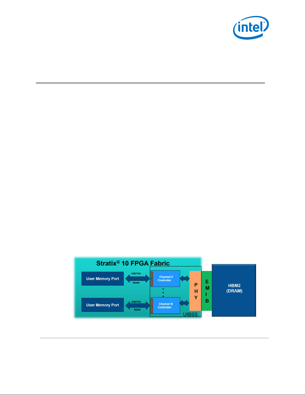
1.1 HBM2 in Intel Stratix 10 MX Devices
Intel Stratix 10 MX incorporates a high-performance FPGA fabric along with a HBM2
DRAM in a single package. Intel Stratix 10 MX devices support up to a maximum of
two HBM2 interfaces.
®
Intel Stratix 10 MX incorporates Intel’s Embedded Multi-Die Interconnect Bridge
(EMIB) technology to implement a silicon bridge between HBM2 DRAM memory and
the Universal Interface Block Subsystem (UIBSS), which contains the HBM2 controller
(HBMC), physical-layer interface (PHY), and I/O ports to interface to the HBM2 stack.
As illustrated below, each Intel Stratix 10 MX device contains a single universal
interface bus per HBM2 interface, supporting 8 independent channels.
The user interface to the HBM2 controller is maintained through the AIX4 protocol.
Sixteen AXI interfaces are available in the user interface from each HBM2 controller,
with one AXI interface available per HBM2 Pseudo Channel. HBM2 DRAM density of
4GB and 8GB are supported.
Figure 1. Intel Stratix 10 MX Device with UIB, EMIB, and HBM2 DRAM
Intel Corporation. All rights reserved. Intel, the Intel logo, Altera, Arria, Cyclone, Enpirion, MAX, Nios, Quartus
and Stratix words and logos are trademarks of Intel Corporation or its subsidiaries in the U.S. and/or other
countries. Intel warrants performance of its FPGA and semiconductor products to current specifications in
accordance with Intel's standard warranty, but reserves the right to make changes to any products and services
at any time without notice. Intel assumes no responsibility or liability arising out of the application or use of any
information, product, or service described herein except as expressly agreed to in writing by Intel. Intel
customers are advised to obtain the latest version of device specifications before relying on any published
information and before placing orders for products or services.
*Other names and brands may be claimed as the property of others.
ISO
9001:2008
Registered
Page 4
1 Introduction to High Bandwidth Memory
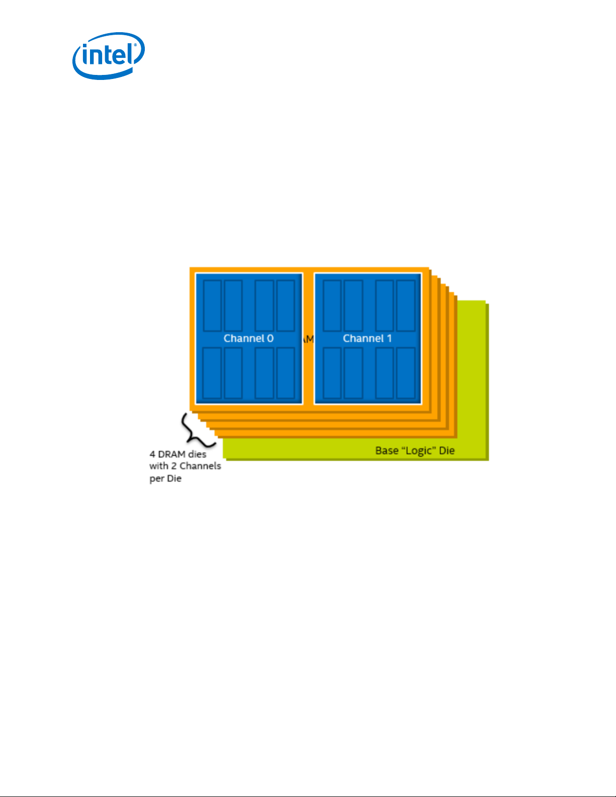
1.2 HBM2 DRAM Structure
The HBM DRAM is optimized for high-bandwidth operation to a stack of multiple DRAM
devices across several independent interfaces called channels. Each DRAM stack
supports up to eight channels.
The following figure shows an example stack containing four DRAM dies, each die
supporting two channels. Each die contributes additional capacity and additional
channels to the stack, up to a maximum of eight channels per stack. Each channel
provides access to an independent set of DRAM banks. Requests from one channel
may not access data attached to a different channel.
Figure 2. High Bandwidth Memory Stack of Four DRAM Dies
UG-20031 | December 2017
1.3 Intel Stratix 10 MX HBM2 Features
Intel Stratix 10 MX FPGAs offer the following HBM2 features.
• Supports one to eight HBM2 channels per HBM2 interface in the Pseudo Channel
mode.
• Each HBM2 channel supports a 128-bit DDR data bus, with optional ECC support.
• Pseudo Channel mode divides a channel into two individual 64-bit data interfaces
per channel. The Pseudo Channels share the same Address and Command bus,
but decodes and executes commands individually.
•
Data referenced to strobes RDQS_t / RDQS_c and WDQS_t / WDQS_c, one strobe
pair per 32 DQs.
•
Differential clock inputs (CK_t / CK_c). Unterminated data/address/cmd/clk
interfaces.
Intel® Stratix® 10 MX HBM2 IP User Guide
4
Page 5

1 Introduction to High Bandwidth Memory
UG-20031 | December 2017
•
DDR commands entered on each positive CK_t and CK_c edge. Row Activate
commands require two memory cycles; all other command are single-cycle
commands.
• Supports command, write data and read data parity.
• Support for bank grouping.
• Support for data bus inversion.
• Data mask for masking write data per byte. (Not available with ECC.)
• I/O voltage of 1.2V and DRAM core voltage of 1.2V.
1.4 Intel Stratix 10 MX HBM2 Controller Features
Intel Stratix 10 MX FPGAs offer the following controller features.
• User applications communicate with the HBMC using the AXI4 Protocol.
• There is one AXI4 interface per HBM2 Pseudo Channel. Each HBM2 interface
supports a maximum of sixteen AXI4 interfaces to the sixteen Pseudo Channels.
• The full-rate user interface can operate at a frequency lower than the HBM2
interface frequency For information on supported clock frequencies, refer to Intel
Stratix 10 MX HBM2 Supported Frequencies in Intel Stratix 10 MX HBM2 IP
Controller Interface Signals.
• The controller offers 32B and 64B access granularity supporting burst length 4 (BL
4) and pseudo-BL 8 (two back to back BL4).
• The controller offers out-of-order command scheduling and read data reordering.
• The controller supports a user-initiated refresh command (enabled through the
side band Advanced Peripheral Bus (APB) interface).
• The controller supports data mask or error correction code (ECC). When you do
not use data mask or ECC, you may use those bits as additional data bits.
Related Links
Clock Signals on page 30
Intel® Stratix® 10 MX HBM2 IP User Guide
5
Page 6

UG-20031 | December 2017
2 Intel Stratix 10 MX HBM2 Architecture
This chapter provides an overview of the Intel Stratix 10 MX HBM2 architecture.
2.1 Intel Stratix 10 MX HBM2 Introduction
Intel Stratix 10 MX devices use the Intel EMIB technology to interface to the HBM2
memory devices.
• The Intel Stratix 10 MX FPGAs offer up to two HBM2 interfaces.
• Each HBM2 device can have a device density of 4GB or 8GB, based on the FPGA
chosen.
This system-in-package solution helps to achieve maximum bandwidth and low power
consumption in a small footprint.
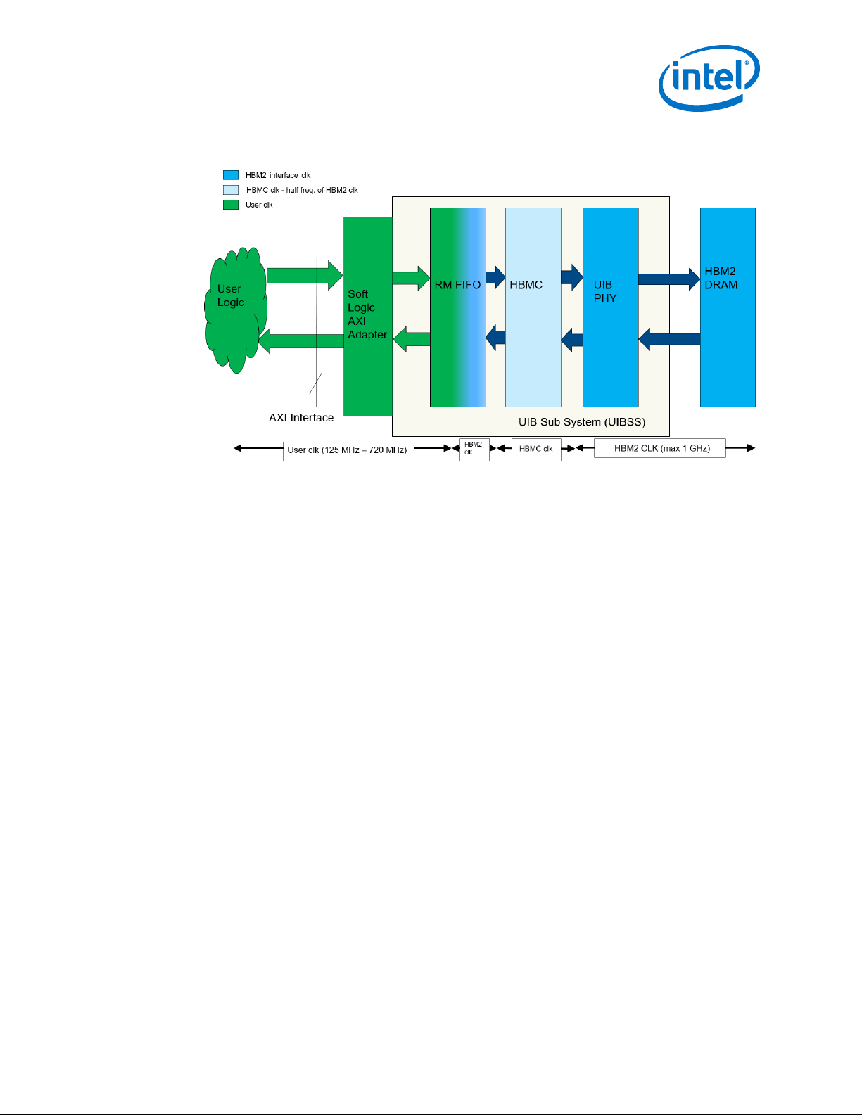
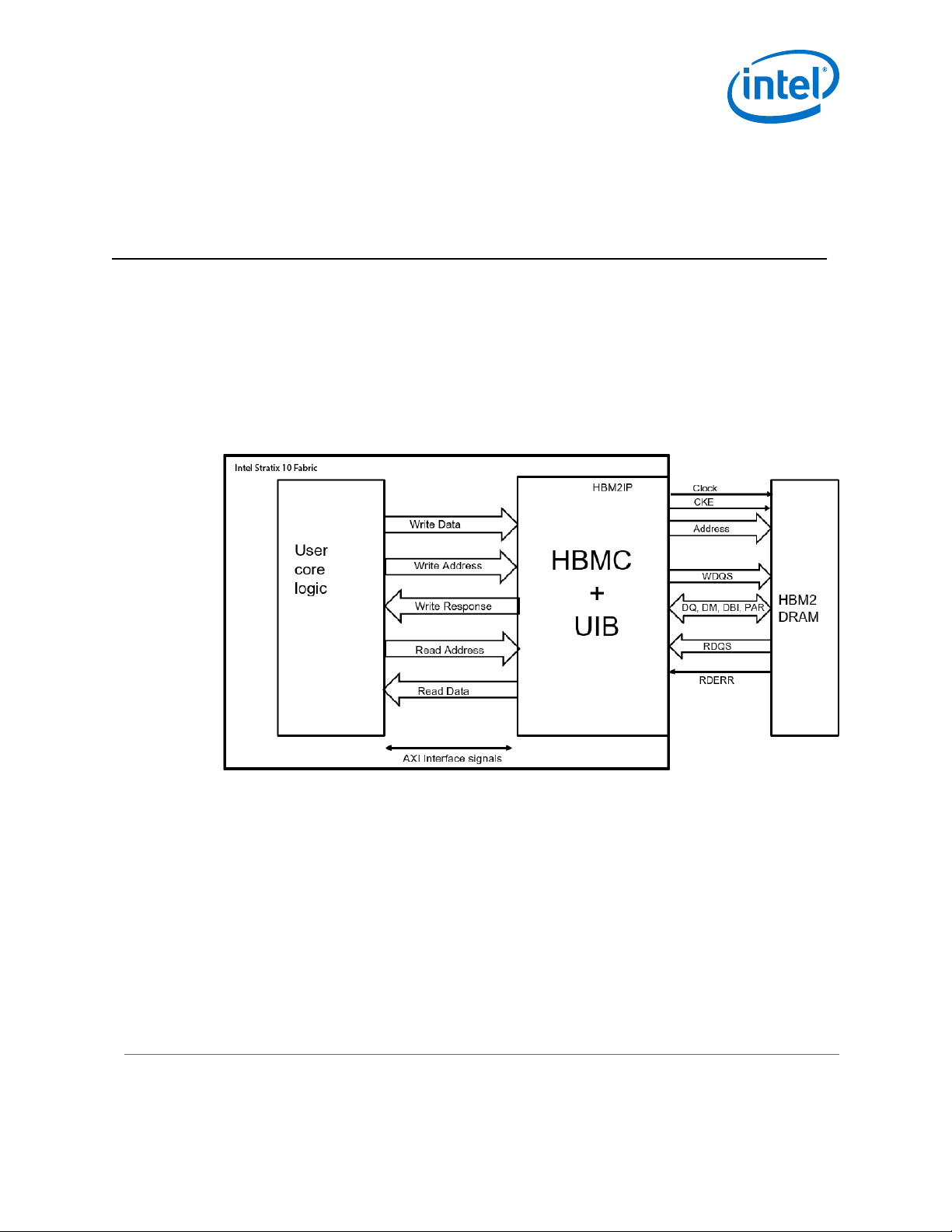
2.2 Intel Stratix 10 MX HBM2 Architecture
The Intel Stratix 10 MX device architecture includes the universal interface bus (UIB)
subsystem (UIBSS) which contains the necessary logic to interface the FPGA core to
the HBM2 DRAM.
Each UIB subsystem includes the HBM2 hardened controller and the universal
interface bus, consisting of the hardened physical interface and I/O logic needed to
interface to each HBM2 DRAM device. The AMBA AXI4 protocol interfaces the core
logic with the universal interface bus subsystem. An optional soft logic adapter
implemented in the FPGA fabric helps to efficiently interface user logic to the hardened
HBM2 controller.
The following figure shows a high-level block diagram of the Intel Stratix 10 HBM2
universal interface bus subsystem. The UIB subsystem includes the following
hardened logic:
• Rate-matching FIFOs that transfer logic from the user core clock to the HBM2
clock domain.
• HBM2 memory controller (HBMC).
• UIB PHY, including the UIB physical layer and I/O.
Intel Corporation. All rights reserved. Intel, the Intel logo, Altera, Arria, Cyclone, Enpirion, MAX, Nios, Quartus
and Stratix words and logos are trademarks of Intel Corporation or its subsidiaries in the U.S. and/or other
countries. Intel warrants performance of its FPGA and semiconductor products to current specifications in
accordance with Intel's standard warranty, but reserves the right to make changes to any products and services
at any time without notice. Intel assumes no responsibility or liability arising out of the application or use of any
information, product, or service described herein except as expressly agreed to in writing by Intel. Intel
customers are advised to obtain the latest version of device specifications before relying on any published
information and before placing orders for products or services.
*Other names and brands may be claimed as the property of others.
ISO
9001:2008
Registered
Page 7
2 Intel Stratix 10 MX HBM2 Architecture
UG-20031 | December 2017
Figure 3. Block Diagram of Intel Stratix 10 MX HBM2 Implementation
The user core clock drives the logic highlighted in green, while the UIB clocks the logic
highlighted in blue. The UIB clock also drives the HBM2 interface clock. User logic can
run up to one-to-four times slower than the HBM2 interface.
Soft Logic AXI Adaptor
The HBM2 IP also includes a soft logic adaptor implemented in core logic. The soft
logic adaptor gates the user valid signals (write address valid, write data
valid, and read address valid) with the corresponding pipelined ready signals
from the HBM2 controller. The soft logic adapter also temporarily stores output from
the HBM2 controller (AXI write response and AXI read data channels) when the AXI
ready signal is absent. You can disable the temporary storage logic if user logic is
always ready to accept output from the HBM2 controller through the parameter editor
when generating the HBM2 IP.
HBM2 DRAM
The HBM2 DRAM is ideal for high-bandwidth operation to multiple DRAM devices
across many independent interfaces called channels. Each channel provides access to
an independent set of DRAM banks. Requests from one channel cannot access data
attached to another channel.
Each HBM2 channel consists of an independent command and data interface to and
from the HBM2 DRAM. A channel provides access to a discrete pool of memory in the
DRAM device; no channel can access the memory storage for another channel. Each
channel interface provides an independent interface to a specific number of banks of
DRAM of a defined page size.
The following table lists the HBM2 signals that interface to the UIB. The UIB drives the
HBM2 signals and decodes the received data from the HBM2. These signals cannot be
accessed through the AXI4 User Interface.
Intel® Stratix® 10 MX HBM2 IP User Guide
7
Page 8

2 Intel Stratix 10 MX HBM2 Architecture
UG-20031 | December 2017
Table 1. Summary of Per-channel Signals
Signal Name Signal Width Notes
Data 128 128 bit bidirectional DQ per channel
Column command/address 8 8-bit wide column address bits
Row command/address 6 6-bit wide row address bits
DBI 16 1 DBI per 8 DQs
DM_CB 16 1 DM per 8 DQs. You can use these
PAR 4 1 parity bit per 32 DQs
DERR 4 1 data error bit per 32 DQs
Strobes 16 Separate strobes for read and write
Clock 2 Clocks address and command signals
CKE 1 Clock enable
AERR 1 Address error
pins for DM or ECC, but not both.
strobes. One differential pair per 32
DQs for read and write.
The following table lists the HBM2 signals that are common to all Pseudo Channels in
each HBM2 interface. The HBM2 controller interfaces with the following signals; these
signals are not available at the AXI4 user interface.
Table 2. Summary of Global HBM2 Signals
Signal Name Signal Width Notes
Reset 1 Reset input
TEMP 3 Temperature output from HBM2.
Cattrip 1 Catastrophic temperature sensor.
The Intel Stratix 10 MX HBM2 IP supports only the Pseudo Channel mode of the HBM2
specification. Pseudo Channel mode includes the following features:
• Pseudo Channel mode divides a single HBM2 channel into two individual
subchannels of 64 bit I/O.
• Both Pseudo Channels share the channel’s row and column command bus, CK, and
CKE inputs, but decode and execute commands individually.
• Pseudo Channel mode requires a burst length of 4.
• Address BA4 directs commands to either Pseudo Channel 0 (BA4 = 0) or Pseudo
Channel 1 (BA4 = 1). The HBM2 controller handles the addressing requirements of
the Pseudo Channels.
• Power-down and self-refresh are common to both Pseudo Channels, due to a
shared CKE pin. Both Pseudo Channels also share the channel’s mode registers.
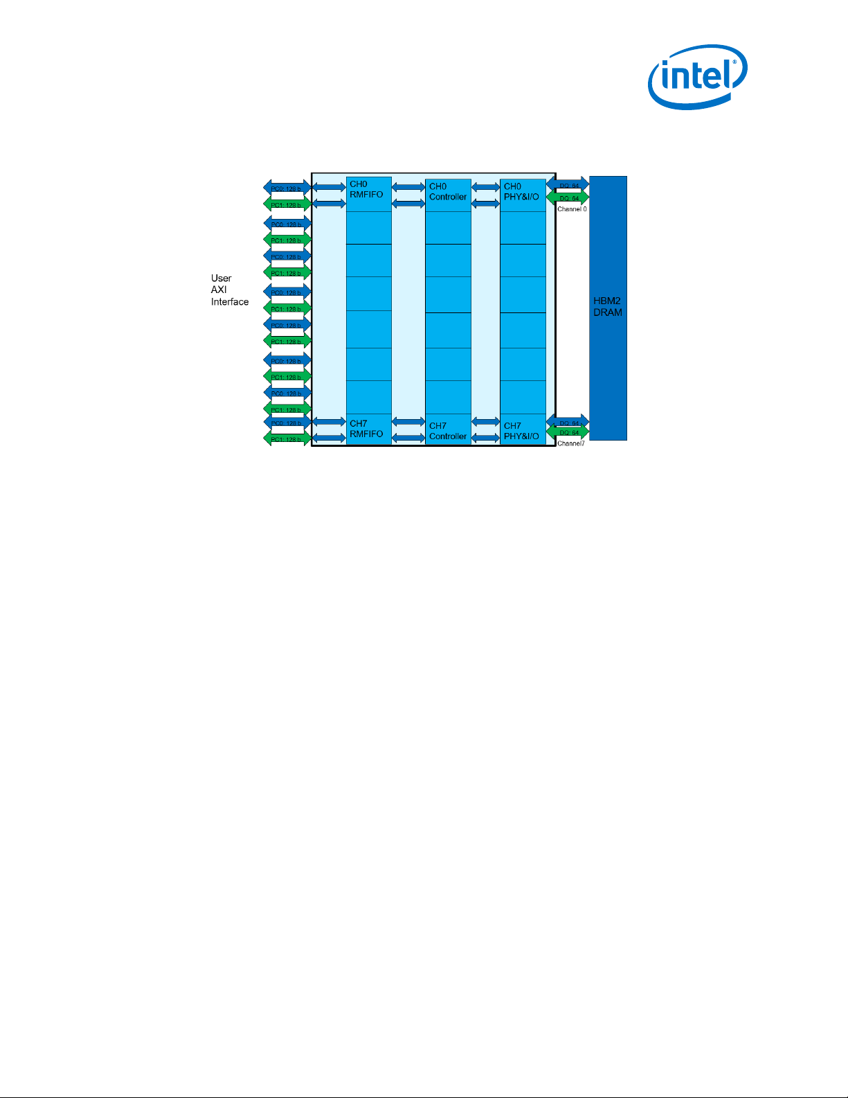
Each Intel Stratix 10 MX HBM2 interface supports a maximum of eight HBM2 channels.
Each HBM2 channel has two AXI4 interfaces, one per Pseudo Channel. The following
figure shows the flow of data from user logic to the HBM2 DRAM through the UIBSS,
while selecting HBM2 channels 0 and 7.
Intel® Stratix® 10 MX HBM2 IP User Guide
8
Page 9
2 Intel Stratix 10 MX HBM2 Architecture
UG-20031 | December 2017
Figure 4. Intel Stratix 10 MX HBM2 Interface Using HBM2 Channels 0 and 7 through
the UIBSS
There is one AXI interface per Pseudo Channel. The AXI4 protocol can handle
concurrent writes and reads to the HBM2 controller. There is also a sideband user port
per user channel pair, compliant to the Advanced Peripheral Bus (APB). The sideband
provides access to user-controlled features such as refresh requests.
Related Links
Intel Stratix 10 MX HBM2 Controller Details on page 10
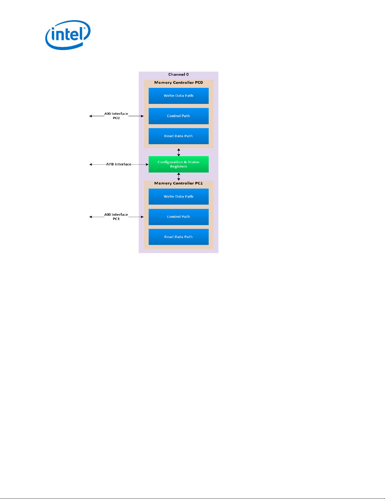
2.3 Intel Stratix 10 MX HBM2 Controller Architecture
The hardened HBM2 controller provides a controller per Pseudo Channel.
Each controller consists of a write and read data path and the control logic that helps
to translate user commands to the HBM2 memory. The control logic accounts for the
HBM2 memory specification timing and schedules commands in an efficient manner.
The following figure shows a block diagram of the HBM2 controller, corresponding to
channel 0. Each channel consists of two AXI ports (one per Pseudo Channel), and a
sideband APB interface, which lets you issue requests, such as auto-refresh, to the
HBM2.
Intel® Stratix® 10 MX HBM2 IP User Guide
9
Page 10
2 Intel Stratix 10 MX HBM2 Architecture
Figure 5. Intel Stratix 10 MX HBM2 Controller Block Diagram
UG-20031 | December 2017
2.3.1 Intel Stratix 10 MX HBM2 Controller Details
This topic explains some of the high level HBM2 controller features.
HBM2 burst transactions
The HBM2 controller supports only the Pseudo Channel mode of accessing the HBM2
device; consequently, it can only support BL4 transactions to the DRAM. For improving
efficiency, it supports the pseudo-BL8 mode, which helps to provide two back-to-back
BL4 data using a given start address, similar to a BL8 transaction.
Each BL4 transaction corresponds to 4*64 bits or 32 bytes and a BL8 transaction
corresponds to 64 bytes per Pseudo Channel. You can select the burst transaction
mode (32 B vs 64B) through the parameter editor.
The user logic can interface to a maximum of 16 Pseudo Channels (16 AXI ports) per
HBM2 interface. Each AXI port has a separate write and read interface, and can handle
write and read requests concurrently at the same clock. Each write and read data
interface per AXI port is 128 bits wide.
User interface vs HBM2 Interface Frequency
The user interface runs at a frequency lower than the HBM2 interface; the maximum
interface frequency depends on the chosen device speed grade and the FPGA core
logic frequency. The rate-matching FIFOs within the UIB subsystem handle the data
transfer between the two clock domains.
Intel® Stratix® 10 MX HBM2 IP User Guide
10
Page 11

2 Intel Stratix 10 MX HBM2 Architecture
UG-20031 | December 2017
The user interface runs at full rate – that is, data provided on the AXI write or read
data bus on each user clock cycle corresponds to that required in one HBM2 memory
clock cycle.
Command Priority
You can set command priority for a write or read command request through the AXI
interface, through the qos signal in the AXI write address channel, or in the AXI read
address channel. The HBM2 controller supports normal and high priority levels. The
system executes commands with the same priority level in a round-robin scheme.
Starvation limit
The controller tracks how long each command waits and leaves no command
unserviced in the command queue for a long period of time. The controller ensures
that it serves every command efficiently.
Command scheduling
The HBM2 controller schedules the incoming commands to achieve maximum
efficiency at the HBM2 interface. The HBM2 controller also follows the AXI ordering
model of the AXI4 protocol specification.
Data re-ordering
The controller can reorder read data to match the order of the read requests.
Address ordering
The HBM2 controller supports different address ordering schemes that you can select
for best efficiency given your use case. The chosen addressing scheme determines the
order of address configurations in the AXI write and read address buses, including row
address, column address, bank address, and stack ID (applicable only to the 8H
devices). The HBM2 controller remaps the logical address of the command to physical
memory address.
Intel® Stratix® 10 MX HBM2 IP User Guide
11
Page 12

2 Intel Stratix 10 MX HBM2 Architecture
UG-20031 | December 2017
Thermal Control
The HBM2 controller uses the TEMP and CATTRIP outputs from the HBM2 device to
manage temperature variations in the HBM2 interface.
• Temperature compensated refresh (TEMP): The HBM2 DRAM provides temperature
compensated refresh information to the controller through the TEMP[2:0] pins,
which defines the proper refresh rate that the DRAM expects to maintain data
integrity. Absolute temperature values for each encoding are vendor-specific. The
encoding on the TEMP[2:0] pins reflects the required refresh rate for the hottest
device in the stack. The TEMP data updates when the temperature exceeds
vendor-specified threshold levels appropriate for each refresh rate.
• Catastrophic temperature sensor (CATTRIP): The CATTRIP sensor detects whether
the junction temperature of any die in the stack exceeds the catastrophic trip
threshold value CATTEMP. The device vendor programs the CATTEMP to a value
less than the temperature at which permanent damage to the HBM stack would
occur.
If a junction temperature anywhere in the stack exceeds the CATTEMP value, the
HBM stack drives the external CATTRIP pin to 1, indicating that catastrophic
damage may occur. When the CATTRIP pin is at 1, the controller stops all traffic to
HBM and stalls indefinitely. To resolve the overheating situation and return the
CATTRIP value to 0, remove power from the device and allow sufficient time for
the device to cool before again applying power.
• Thermal throttling: Thermal throttling is a controller safety feature that helps
control thermal runaway if the HBM2 die overheats, preventing a catastrophic
failure. You can specify the HBM2 device junction temperature at which the
controller begins to throttle input commands, and the throttle ratio that
determines the throttle frequency. The controller deasserts the AXI ready signals
(awready, wready and arready) when it is actively throttling the input
commands and data.
Refresh requests
The HBM2 controller handles HBM2 memory refresh requirements and issues refresh
requests at the optimal time. The controller automatically controls refresh rates based
on the temperature setting of the memory through the TEMP vector that the memory
provides. You can select the HBM2 controller refresh policy, based on the frequency of
refresh requests. You can choose to issue refresh commands directly, through the
sideband APB interface.
Precharge policy
The HBM2 controller issues precharge commands to the HBM2 memory based on the
write/read transaction address. In addition, you can issue an auto-precharge
command together with a write and read command, through the AXI write address
port and AXI read address port.
There are two auto-precharge modes:
• HINT – You can issue the auto-precharge request. The controller then decides
when to issue the precharge command.
• FORCED – You provide auto-precharge requests through the AXI interface and the
precharge request executes.
Intel® Stratix® 10 MX HBM2 IP User Guide
12
Page 13

2 Intel Stratix 10 MX HBM2 Architecture
UG-20031 | December 2017
Power down enable
To conserve power, the HBM2 controller can enter power-down mode when the bus is
idle for a long time. You can select this option if required.
HBM2 Controller features enabled by default
The HBM2 controller enables the following features by default:
• DBI – The DBI option supports both write and read DBI, and optimizes SI/power
consumption by restricting signal switching on the HBM2 DQ bus.
• Parity – Supports command/address parity and DQ parity.
Related Links
• Clock Signals on page 30
• Intel Stratix 10 MX HBM2 Architecture on page 6
Intel® Stratix® 10 MX HBM2 IP User Guide
13
Page 14
UG-20031 | December 2017
3 Generating the Intel Stratix 10 MX HBM2 IP
You can generate and parameterize the HBM2 IP using the Intel Quartus® Prime Pro
Edition software, version 17.1 and later.
1. Before generating the HBM2 IP, you must create a new project:
a. Launch the Intel Quartus Prime Pro Edition software.
b.
Launch the New Project Wizard by clicking File ➤ New Project Wizard.
c. Type a name for your project in the Directory, Name, Top-Level Entity
field.
d. In the Project Type section, select Empty Project.
e. In the Add Files section, click Next.
f. In the Family, Device, and Board Settings section, select Stratix 10 MX
as the device family.
g. Under Available Devices, select any MX device and your desired speed
grade.
h. Click Next and follow the Wizard's prompts to finish creating the project.
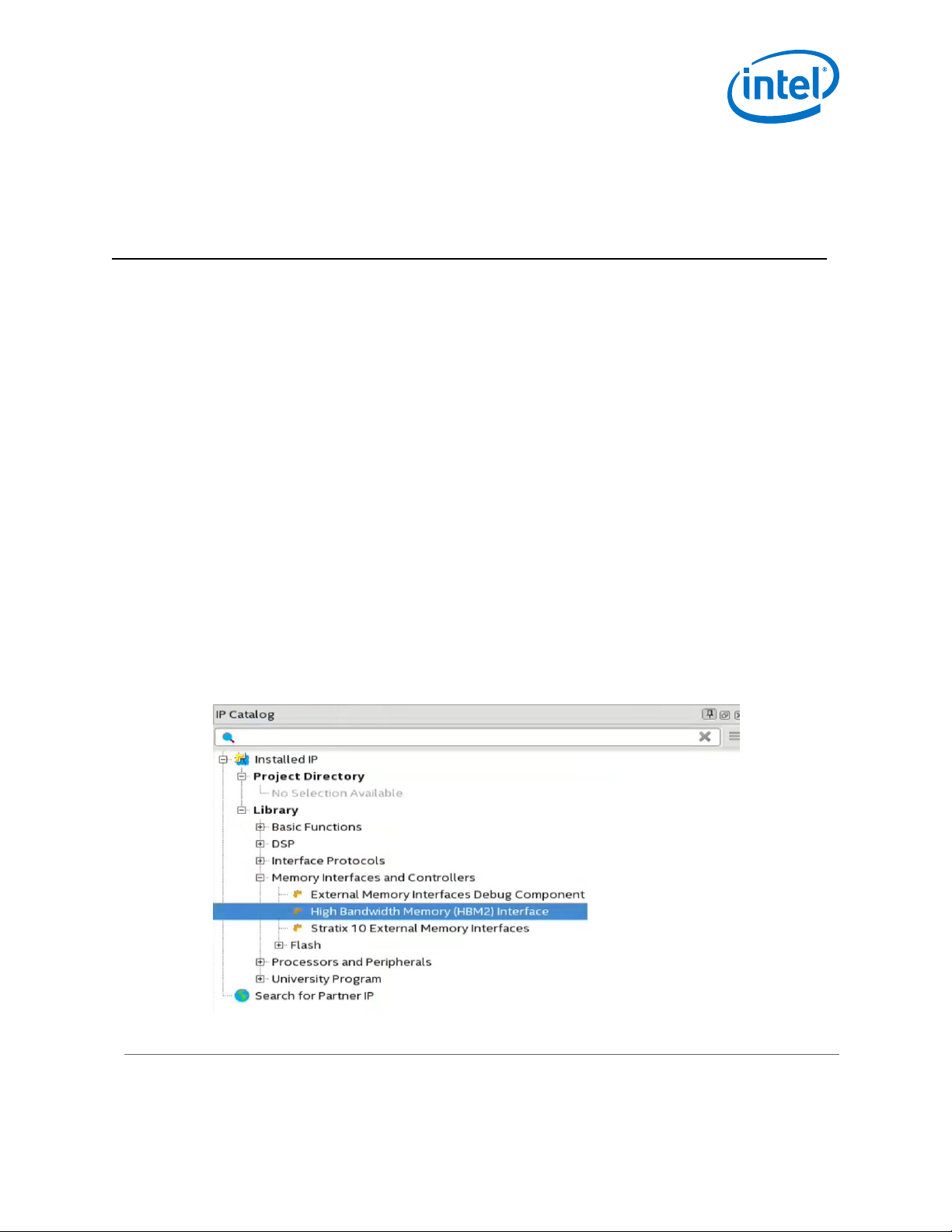
2.
In the IP Catalog, open Library ➤ Memory Interfaces and Controllers.
3. Select High Bandwidth memory (HBM2) Interface and launch the parameter
editor.
Figure 6. Selecting High Bandwidth Memory Interface in the IP Catalog
Intel Corporation. All rights reserved. Intel, the Intel logo, Altera, Arria, Cyclone, Enpirion, MAX, Nios, Quartus
and Stratix words and logos are trademarks of Intel Corporation or its subsidiaries in the U.S. and/or other
countries. Intel warrants performance of its FPGA and semiconductor products to current specifications in
accordance with Intel's standard warranty, but reserves the right to make changes to any products and services
at any time without notice. Intel assumes no responsibility or liability arising out of the application or use of any
information, product, or service described herein except as expressly agreed to in writing by Intel. Intel
customers are advised to obtain the latest version of device specifications before relying on any published
information and before placing orders for products or services.
*Other names and brands may be claimed as the property of others.
ISO
9001:2008
Registered
Page 15

3 Generating the Intel Stratix 10 MX HBM2 IP
UG-20031 | December 2017
3.1 Parameterizing the Intel Stratix 10 MX HBM2 IP
You can parameterize your HBM2 IP with the HBM2 IP parameter editor.
The parameter editor comprises the following tabs, on which you set the parameters
for your IP:
• General
• Controller
• Diagnostics
• Example Designs
3.2 General Parameters for Intel Stratix 10 MX HBM2 IP
The General tab allows you to select the channels that you want to implement, and to
select the memory and fabric core clock frequency.
Figure 7. General Tab
Intel® Stratix® 10 MX HBM2 IP User Guide
15
Page 16

3 Generating the Intel Stratix 10 MX HBM2 IP
UG-20031 | December 2017
Table 3. Group: General / FPGA
Display Name Description
Speed Grade Specifies the speed grade of the Intel Stratix 10 FPGA.
HBM2 Device Type Select the HBM2 Memory Device: 4GB/4H refers to HBM2
HBM2 Location Selects the location of the HBM2 interface in the Intel
device with a total device density of 4GB in a 4-high Stack,
and 8GB8H refers to a total HBM2 device density of 8GB in
an 8-high Stack.
Stratix 10 FPGA.
Table 4. Group: General / HBM2 Interface
Display Name Description
Add Controller for HBM Channel 0 ––– 7 Allows you to select the HBM2 memory channels that you
want to implement. Each HBM2 channel supports a 128-bit
interface to the HBM2 device, using two 64-bit Pseudo
Channels.
The user interface to the HBM2 Controller uses the AXI4
protocol. Each Controller has one AXI4 interface per Pseudo
Channel or 2 AXI4 interfaces per channel.
Table 5. Group: General / AXI Interface
Display Name Description
Allow backpressure of AXI read data and write response
channels
Threshold temperature for AXI throttling This parameter defines the temperature, in degrees Celsius,
AXI throttling rate If you enable AXI interface throttling based on temperature,
Instantiates FIFOs in soft logic to buffer read data and write
response on the AXI interfaces. Enable this parameter if
user logic ever deasserts the AXI rready/bready signals.
You can disable this parameter to reduce latency, but only if
you never use rready/bready to backpressure the
interface.
above which the HBM2 controller throttles AXI interface
transactions. The temperature setting applies to all the AXI4
interfaces; however, you must enable this feature on the
corresponding controller tab of each HBM2 controller. When
you enable throttling, the HBM2 controller reduces the
amount of traffic on the DRAM channel.
this parameter defines the throttle ratio as a percentage (0:
no throttling, 100: full throttling).
Table 6. Group: General / Clocks
Display Name Description
Memory clock interface Specifies the clock frequency for the HBM2 interface. The
Use recommended PLL reference clock frequency Automatically calculates the PLL reference clock frequency
PLL reference clock frequency Enable this parameter only if you disable Use
maximum supported HBM2 clock frequency depends on the
FPGA device speed grade:
• -1 Speed grade : 1 GHz
• -2 Speed grade : 800 MHz
• -3 Speed grade : 600 MHz
for best performance. You should disable this parameter if
you want to select a different PLL reference clock frequency
recommended PLL reference clock frequency, and
want to specify a PLL reference clock frequency. You can
continued...
Intel® Stratix® 10 MX HBM2 IP User Guide
16
Page 17

3 Generating the Intel Stratix 10 MX HBM2 IP
UG-20031 | December 2017
Display Name Description
select a PLL reference clock frequency from a displayed list.
The values in the list can change when the memory
interface frequency changes or the clock rate of user logic
changes. You should use the fastest possible PLL reference
clock frequency to achieve best jitter performance.
Core clock frequency Specifies the clock frequency at which the FPGA core logic
Use recommended example design core clock PLL reference
clock frequency
Reference clock frequency for example design core clock
PLL
of the AXI4 interface operates. A separate PLL is required to
generate the core clock. The maximum supported core
frequency depends on the device speed grade and timing
closure of this clock within the FPGA. The minimum
frequency of the core clock is one-fourth the HBM2 interface
frequency.
Automatically calculates the example design core clock PLL
reference clock frequency for best performance. Disable this
parameter if you want to select a different reference clock
frequency.
Specify the externally provided reference clock frequency
for the core clock PLL.
Related Links
Clock Signals on page 30
3.3 Controller Parameters for Intel Stratix 10 MX HBM2 IP
The parameter editor contains one Controller tab for each memory channel that you
specify on the General tab. The Controller tab allows you to select the HBM2
controller options that you want to enable.
Figure 8. Controller Tab
Intel® Stratix® 10 MX HBM2 IP User Guide
17
Page 18

3 Generating the Intel Stratix 10 MX HBM2 IP
UG-20031 | December 2017
Table 7. Group: Controller/ Controller 0 Configuration
Display Name Description
Is clone of Specifies a controller from which to copy all parameter
Enable Re-order buffer Specifies that read data returns to the user interface in the
Enable AXI interface throttling based on temperature and
cattrip
Address reordering Specifies the pattern for mapping from the AXI interface to
User Read Auto-Precharge Policy You can issue the request to precharge together with the
User Write Auto-Precharge Policy You can issue a precharge request together with the write
values; this parameter applies when you select more than
one HBM2 controller. Set this parameter if you want one
controller to have the same settings as another.
same order as the issued read commands. If you disable
this feature, the controller may read data in a different
order than it is written; you must maintain the order, based
on the AXI read ID of the transaction.
This parameter applies to cases with multiple AXI
transaction IDs. By using different AXI read/write IDs, you
allow the HBM2 controller to reorder transactions for better
efficiency. If you use the same AXI ID for all transactions,
the controller issues the commands to memory in the order
in which they arrive; in this instance, you need not enable
the reorder buffer.
Enables AXI thermal throttling for the specific HBM2
controller. The parameter that sets the trigger temperature
for thermal throttling resides on the General tab.
the HBM2 memory device. By choosing the right address
reordering configuration, you help to improve the efficiency
of accesses to the HBM2 memory device, based on user
traffic pattern. The HBMC supports three types of address
reordering:
Address order (32B access: pseudo-BL8 disabled):
SID-BG-BANK-ROW-COL[5:1]
SID-ROW-BANK-COL[5:1]-BG
ROW-SID-BANK-COL[5:1]-BG
COL[0]=0
Address order (64B access (pseudo-BL8 enabled):
SID-BG-BANK-ROW-COL[5:1]
SID-ROW-BANK-COL[5:2]-BG-COL[1]
ROW-SID-BANK-COL[5:2]-BG-COL[1]
COL[1:0] = {00})
SID applies only to the 8GB/8H HBM2 devices and is not
available for 4GB/4H devices.
read command, through the axi_x_y_aruser input, where
x denotes the HBM2 channel number (0-7) and y denotes
the HBM2 Pseudo Channel number (0/1).
You can choose between two values for this parameter:
• RDAP_FORCED mode, in which the HBM2 controller
implements a user-requested auto-precharge command.
• RDAP_HINT mode, in which the controller determines
when to issue an auto-precharge command, based on
user-issued auto-precharge input and the address
specified.
command, through the axi_x_y_awuser input, where x
denotes the HBM2 channel number (0-7) and y denotes the
HBM2 Pseudo Channel number (0/1).
continued...
Intel® Stratix® 10 MX HBM2 IP User Guide
18
Page 19

3 Generating the Intel Stratix 10 MX HBM2 IP
UG-20031 | December 2017
Display Name Description
You can choose between two values for this parameter:
• WRAP_FORCED mode, in which the HBM2 controller
implements a user-requested auto-precharge command.
• WRAP_HINT mode, in which the controller determines
when to issue an auto-precharge command, based on
user-issued auto-precharge input and the address
specified.
Power Down Enable Allows the controller to power down when there are no
Refresh mode Specifies how the HBM2 controller receives refresh
Refresh policy Specifies how the controller issues refresh commands, when
Enable 64B access for performance Enable this parameter for 64 bit (burst length 8) data
Width of User Data Specifies the data width to use. The default setting is 256
Memory channel ECC generation and checking/correction The HBM2 controller supports single-bit error correction and
Write data mask enable Enables the write data mask (DM) input to the HBM2 DRAM.
commands in the queue for a long period of time.
requests:
• The default value is Controller refresh all, which
allows the controller to decide when to issue refresh
requests.
• Alternatively, you can issue refresh requests through the
APB sideband interface, to all or specific banks.
you set Refresh mode to Controller refresh all.
• The default Flexible setting allows the controller to
determine when to issue refresh requests.
• The Pre-pay setting allows the controller to issue
refresh commands earlier when the controller is idle.
• The Post-pay setting allows the controller to postpone
refresh commands until there are no pending requests,
or when it is time to issue a refresh command. Select
this setting in bandwidth-sensitive applications.
transfer through the Pseudo Channel between the UIB and
the HBM2 device.
For 32-bit (burst length 4) data transfer, disable this
parameter.
bits for each HBM2 channel.
Optionally, if you are not using the ECC or DM pins, you can
specify the entire 288 bits for data.
double-bit error detection.
The controller does not support write data mask in ECC
generation mode.
When you use the DM pins, you cannot use ECC.
3.4 Diagnostic Parameters for Intel Stratix 10 MX HBM2 IP
The Diagnostics tab allows you to select traffic options and to enable the efficiency
monitor that measures HBM2 controller efficiency during functional simulation.
Intel® Stratix® 10 MX HBM2 IP User Guide
19
Page 20

3 Generating the Intel Stratix 10 MX HBM2 IP
UG-20031 | December 2017
Figure 9. Diagnostics Tab – Enabling Default Traffic Pattern
Figure 10. Diagnostics Tab – Enabling User-Configured Traffic Pattern
Table 8. Group: Diagnostics / Traffic Generator
Display Name Description
Run the default traffic pattern Runs the default traffic pattern after reset. The default
Run the user-configured traffic stage Enable this parameter if you want to run a custom traffic
Force traffic generator to issue traffic with different read/
write IDs
Intel® Stratix® 10 MX HBM2 IP User Guide
20
traffic pattern consists of sequential transactions.
pattern after reset.
The traffic generator does not assert a pass or fail until you
configure it and signal it to start through its Avalon
configuration interface.
To configure the traffic generator, you connect using the
EMIF Debug Toolkit, or through custom logic connected to
the Avalon-MM configuration slave port on the traffic
generator.
You can simulate configuration using the example testbench
provided in the altera_hbm_tg_axi_tb.sv file.
Causes the traffic generator to issue traffic with different
read/write IDs, regardless of whether you enable the
reorder buffer on the Controller tab. When you do enable
the reorder buffer, the traffic generator automatically
generates transactions with different IDs.
The use of different read/write IDs results in higher
efficiency, but – because the traffic generator logic does not
handle read data returning out-of-order – data mismatches
in simulation can result if you disable the reorder buffer.
Page 21

3 Generating the Intel Stratix 10 MX HBM2 IP
UG-20031 | December 2017
Table 9. Group: Diagnostics / Performance
Display Name Description
Enable Efficiency Monitor Adds an efficiency monitor component to the AXI interface
Enable Efficiency Test Mode Configures the traffic generator to send reads and writes
of the memory controller. The efficiency monitor reports
statistics about the efficiency of the interface during
simulation.
without verifying that read data matches write data. This
parameter increases efficiency by allowing transactions to
execute sooner; however, data mismatches may occur.
3.5 Example Designs Parameters for Intel Stratix 10 MX HBM2 IP
The Example Designs tab allows you to configure example design files for simulation
and synthesis.
Figure 11. Example Designs tab of HBM2 IP Parameters
Table 10. Group: Example Designs / Example Design Files
Display Name Description
Simulation Specifies that the system generate all necessary file sets for
Synthesis
simulation when you click Generate Example Design.
Expect an additional 1-2 minute delay when generating the
simulation fileset.
If you do not enable this parameter, the system does not
generate simulation file sets. Instead, the output directory
contains the ed_sim.qsys file which contains details of the
simulation example design for Platform Designer, and a
make_sim_design.tcl file with other corresponding tcl
files.
You can run the make_sim_design.tcl file from a
command line to generate a simulation example design. The
generated example designs for various simulators reside in
the /sim subdirectory.
Specifies that the system generate all necessary file sets for
synthesis when you click Generate Example Design.
Expect an additional 1-2 minute delay when generating the
synthesis file set.
If you do not enable this parameter, the system does not
generate synthesis file sets. Instead, the output directory
contains the ed_synth.qsys file which contains details of
continued...
Intel® Stratix® 10 MX HBM2 IP User Guide
21
Page 22

3 Generating the Intel Stratix 10 MX HBM2 IP
UG-20031 | December 2017
Display Name Description
the synthesis example design for Platform Designer, and a
make_qii_design.tcl file with other corresponding tcl
files.
You can run the make_qii_design.tcl file from a
command line to generate a synthesis example design. The
generated example design resides in the /qii subdirectory.
Tip: The example design supports generation, simulation, and Intel Quartus Prime
compilation flows for any selected device. To use the example design for simulation,
enable the Simulation parameter. To use the example design for compilation and
hardware, enable the Synthesis parameter.
Table 11. Group: Example Designs / Generated HDL Format
Display Name Description
Simulation HDL format Specifies the HDL format of the example design file set that
you want to generate.
3.6 Generating the Example Design
After you finish parameterizing your IP, you can generate the HBM2 example design.
1. On the Example Designs tab, select Simulation/Synthesis in the Example
Design Files group box. (Timing closure is not supported in the 17.1 release.)
2. On the Example Designs tab, select Verilog in the Generated HDL Format
group box.
3. To generate the example design, press the Generate Example Design button, at
the top-right of the parameter editor.
4. When prompted, specify a location at which to save the generated example design
file set.
5. Press OK to begin generating the example design file set.
Upon successful generation of the example design, the system creates file sets to
support both synthesis and simulation of the HBM2 IP. The
hbm_0_example_design/sim/ed_sim directory, contains file sets for the supported
simulators and for the Intel Quartus Prime project.
The generated file hierarchy includes:
• IP - all the generated .ip files, based on the relevant parameters set in the
paramter editor.
• SIM - all the files required to simulate the HBM2 IP for the example design. These
files include the modifiable traffic generator design, the abstract representation of
the hardened HBM2 controller and universal interface block (UIB), and a generic
model of the HBM2 DRAM for simulation.
• qii - includes all the files required to compile the HBM2 IP example design in the
Intel Quartus Prime software version 17.1. Timing closure will be supported in a
future release.
Intel® Stratix® 10 MX HBM2 IP User Guide
22
Page 23

3 Generating the Intel Stratix 10 MX HBM2 IP
UG-20031 | December 2017
Figure 12. Example Design Hierarchy
3.7 Intel Stratix 10 MX HBM2 IP Example Design for Synthesis
The top level example design for synthesis is available under <Design Directory>/
hbm_0_example_design/qii/ed_synth/synth/ed_synth.v. The
ed_synth_hbm_0_example_design module is the top-level design module for the
HBM2 IP.
Intel® Stratix® 10 MX HBM2 IP User Guide
23
Page 24

3 Generating the Intel Stratix 10 MX HBM2 IP
UG-20031 | December 2017
Your user logic interfaces to the following signals through the top-level ed_synth.v
module:
• Clocks:
— Reference clock input for the UIB PLL that generates the clocks for the UIBSS
and the HBM2 DRA.
— Reference clock input to the I/O PLL that generates the core clock that runs
the user AXI4 interface logic.
• Resets:
—
hbm_0_example_design_pll_ref_clk_clk
—
hbm_0_example_design_wmcrst_n_in_reset_n
—
hbm_only_reset_in_reset (Not currently supported.)
• HBM2 Boundary Scan Signals: The example design requires the boundary scan
signals to be connected for successful compilation, however they are not used.
These do not require to be driven actively or placed in the pin placement file. This
applies to the following signals:
—
Input signals: m2u_bridge_cattrip, m2u_bridge_temp[2:0],
m2u_bridge_wso[7:0]
—
Output signals: m2u_bridge_reset_n, m2u_bridge_wrst_n,
m2u_bridge_wrck, m2u_bridge_shiftwr, m2u_bridge_capturewr,
m2u_bridge_updatewr, m2u_bridge_selectwir and m2u_bridge_wsi.
• Traffic Generator signals: The example design instantiates one traffic generator
per AXI4 interface, or one Pseudo Channel. The traffic generator drives the AXI4
interface signals in the example design. The status signals are provided as outputs
that you can monitor
— AXI4 interface signals: The user logic interfaces to one AXI4 interface per
Pseudo Channel. Each AXI4 interface provides the signals required to interface
to the Write Address, Write Data, Write Response, Read Address and Read
Data Channels.
— User Side Band Advanced Peripheral Bus (APB) Interface: The HBM2 IP
supports one APB interface per HBM2 Channel. The user side band interface is
not supported in 17.1 and will be supported in a future release.
• Traffic Generator status signals:
—
tg<channel num>_<Pseudo Channel
num>_status_traffic_gen_pass
—
tg<channel num>_<Pseudo Channel
num>_status_traffic_gen_fail
—
tg<channel num>_<Pseudo Channel num>_traffic_gen_timeout
Related Links
• Clock Signals on page 30
• Reset Signals on page 31
• AXI User-interface Signals on page 32
Intel® Stratix® 10 MX HBM2 IP User Guide
24
Page 25

UG-20031 | December 2017
4 Simulating the Intel Stratix 10 MX HBM2 IP
This section describes how to simulate the generated HBM2 IP.
Simulation Assumptions
The parameter settings that you make on the Controller tab affect efficiency during
simulation. In the default configuration, with the default parameter settings, the traffic
generator issues sequential transactions.
Supported Simulators
The HMB2 IP supports the following simulators:
• ModelSim*- Intel FPGA Edition
• ModelSim SE
• Questa* Advanced Simulator
• NCSim*
• Aldec Riviera-PRO*
• Synopsys* VCS
4.1 Intel Stratix 10 MX HBM2 IP Example Design
The following illustration shows a high-level block diagram of the HBM2 example
design that provides the simulation environment for the Intel Stratix 10 MX HBM2 IP
when generated for simulation.
Figure 13. Intel Stratix 10 MX HBM2 IP Generated for Simulation
Intel Corporation. All rights reserved. Intel, the Intel logo, Altera, Arria, Cyclone, Enpirion, MAX, Nios, Quartus
and Stratix words and logos are trademarks of Intel Corporation or its subsidiaries in the U.S. and/or other
countries. Intel warrants performance of its FPGA and semiconductor products to current specifications in
accordance with Intel's standard warranty, but reserves the right to make changes to any products and services
at any time without notice. Intel assumes no responsibility or liability arising out of the application or use of any
information, product, or service described herein except as expressly agreed to in writing by Intel. Intel
customers are advised to obtain the latest version of device specifications before relying on any published
information and before placing orders for products or services.
*Other names and brands may be claimed as the property of others.
ISO
9001:2008
Registered
Page 26

4 Simulating the Intel Stratix 10 MX HBM2 IP
UG-20031 | December 2017
The Traffic Generator emulates a real-world application that writes to, and reads back
from memory and validates the read data. You can modify the traffic generator logic to
fit your traffic pattern or drive the transactions to the HBM2 memory with your own
logic.
Simulation incorporates an abstract model of the hardened HBM2 controller and the
universal interface block (UIB). The HBM2 controller performs data reordering and
enhancement functions, and allows communication between the AXI4 user interface
and the UIB PHY. The universal interface block PHY (UIB PHY) is the physical-layer
interface that carries low-level signaling.
The HBM2 Model is an abstract generic model representative of the HBM2 DRAM for
simulation. This is not a vendor-specific model.
4.2 Simulating Intel Stratix 10 MX HBM2 IP with ModelSim*
1. Launch the ModelSim simulator.
2.
Select File ➤ Change Directoryand navigate to: project_directory/sim/
ed_sim/sim/mentor
3. Verify that the Transcript window is visible; if it is not, display it by selecting
View ➤ Transcript.
4.
In the Transcript window, run source msim_setup.tcl at the bottom of the
ModelSim tool screen.
5.
After the Tcl script finishes running, run ld_debug in the Transcript window. This
command compiles the design files and elaborates the top-level design.
6.
After ld_debug finishes running, the Objects window appears. In the Objects
window, select the signals to simulate by right-clicking and selecting Add Wave
from the context menu.
For example, if you want to see the HBM2 interface signals, select the module
mem0_0 from the Instance window. With mem0_0 selected, go to the Objects
window and select the signals that you want to see. (If the Objects window is not
visible, you can display it by selecting View ➤ Objects.
7.
To run the HBM2 simulation, type run -all.
If the simulation is not visible, select View ➤ Wave. With the Wave window
open, select File ➤ Save Format. Click OK to capture your selected waveforms in
a wave.do file. To display the waveforms, type do wave.do, and then type run
-all.
Whenever you make changes to the design or to the wave.do, you must repeat
step 7 of this procedure. Alternatively, you can combine the instructions into a
script and run that script instead. The following example illustrates a run.do
script containing the necessary commands:
if {[file exists msim_setup.tcl]} {
source msim_setup.tcl
ld_debug
do wave.do
run -all } else { error "The msim_setup.tcl script does not
exist.
Please generate the example design RTL and simulation scripts. See ../../
README.txt
for help." }
Intel® Stratix® 10 MX HBM2 IP User Guide
26
Page 27

4 Simulating the Intel Stratix 10 MX HBM2 IP
UG-20031 | December 2017
Save the run.do script in the same directory as the msim_setup.tcl file. Type
do run.do to run this script from the Transcript window.
8. Upon completion of the simulation, the Transcript window displays efficiency data
and other useful information.
4.3 Simulating Intel Stratix 10 MX HBM2 IP with Synopsys VCS*
1.
Navigate to the project_directory/hbm_0_example_design/sim/
ed_sim/sim/synopsys/vcs directory.
2.
To run the simulation, type sh vcs_setup.sh. To view the simulation results,
write the output to a log file. The simulation log provides efficiency data and other
useful information.
3.
To view the waveform, add +vcs+dumpvars+test.vcd to the vcs command.
4.
To view the waveform, type dve & to launch the waveform viewer. Add the
necessary signals or module to the waveform view to view the required signals.
4.4 Simulating Intel Stratix 10 MX HBM2 IP with Riviera-PRO*
1.
Navigate to: project_directory>/sim/ed_sim/aldec.
2.
Type rungui to launch the Riviera-PRO simulator.
3.
Type source rivierapro_setup.tcl.
4.
Type ld_debug to compile the design files and elaborate the top-level design.
5.
Type run -all to run the HBM2 simulation.
4.5 Simulating Intel Stratix 10 MX HBM2 IP for High Efficiency
The default traffic pattern can achieve high efficiency by efficiently utilizing the HBM2
memory bandwidth and providing an efficient flow of traffic between the HBM2
controller and AXI user interface.
The main steps to deriving higher efficiency are:
• Turn off Enable Reorder Buffer on the Controller tab. The Reorder Buffer
rearranges the read data in the order of the issued requests.
• Turn on Force traffic generator to issue different AXI Read/Write IDs and
Enable Efficiency Test Mode on the Diagnostics tab. In this configuration, the
traffic generator skips the data validation stage based on the different AXI IDs;
consequently, you may receive data mismatch warnings, which you can ignore.
The following sections explain the General, Controller, and Diagnostic tab
parameters required to perform high efficiency HBM2 simulation. The following figures
illustrate parameter settings for a high-efficiency simulation for a single-channel HBM2
controller.
Intel® Stratix® 10 MX HBM2 IP User Guide
27
Page 28

4 Simulating the Intel Stratix 10 MX HBM2 IP
Figure 14. Controller Tab Settings for High Efficiency Simulation
UG-20031 | December 2017
Figure 15. Diagnostics Tab Settings for High Efficiency Simulation
ModelSim
Navigate to the project_directory/sim/ed_sim/sim/mentor directory, open
the msim_setup.tcl file in an editor, and change:
set TOP_LEVEL_NAME "ed_sim.ed_sim"
Intel® Stratix® 10 MX HBM2 IP User Guide
28
Page 29

4 Simulating the Intel Stratix 10 MX HBM2 IP
UG-20031 | December 2017
to
Set TOP_LEVEL_NAME “altera_hbm_tg_axi_171.altera_hbm_tg_axi_tb”
To simulate the design, follow the steps in Simulating HBM2 IP with ModelSim.
Synopsys VCS
Navigate to the project_directory/hbm_0_example_design/sim/
ed_sim/sim/synopsys/vcs directory. Open the vcs_setup.sh file in an editor,
and change:
TOP_LEVEL_NAME="ed_sim"
to
TOP_LEVEL_NAME="altera_hbm_tg_axi_tb"
To simulate the design, follow the steps in Simulating HBM2 IP with Synopsys VCS.
Riviera-PRO
Navigate to the project_directory/sim/ed_sim/aldec directory. Open the
rivierapro_setup.tcl file in an editor, and change:
set TOP_LEVEL_NAME "ed_sim.ed_sim"
to
set TOP_LEVEL_NAME “altera_hbm_tg_axi_171.altera_hbm_tg_axi_tb”
To simulate the design, follow the steps in Simulating HBM2 IP with Riviera-PRO.
Intel® Stratix® 10 MX HBM2 IP User Guide
29
Page 30
UG-20031 | December 2017
5 Intel Stratix 10 MX HBM2 IP Interface
This chapter provides an overview of the signals that interface to the HBM2 IP.
5.1 Intel Stratix 10 MX HBM2 IP High Level Block Diagram
The following figure shows a high-level block diagram of the Intel Stratix 10 MX HBM2
IP. The HBM2 IP communicates with user logic through the AXI protocol.
Figure 16. High Level Block Diagram of HBM2 Implementation
5.2 Intel Stratix 10 MX HBM2 IP Controller Interface Signals
This section lists the signals that connect core logic to the HBM2 IP.
5.2.1 Clock Signals
Each HBM2 interface requires the following refclk clock inputs.
Intel Corporation. All rights reserved. Intel, the Intel logo, Altera, Arria, Cyclone, Enpirion, MAX, Nios, Quartus
and Stratix words and logos are trademarks of Intel Corporation or its subsidiaries in the U.S. and/or other
countries. Intel warrants performance of its FPGA and semiconductor products to current specifications in
accordance with Intel's standard warranty, but reserves the right to make changes to any products and services
at any time without notice. Intel assumes no responsibility or liability arising out of the application or use of any
information, product, or service described herein except as expressly agreed to in writing by Intel. Intel
customers are advised to obtain the latest version of device specifications before relying on any published
information and before placing orders for products or services.
*Other names and brands may be claimed as the property of others.
ISO
9001:2008
Registered
Page 31

5 Intel Stratix 10 MX HBM2 IP Interface
UG-20031 | December 2017
Table 12. Intel Stratix 10 MX HBM2 Required Clock Inputs
Clock Description Clock Guidelines
core_clk_iopll_ref_clk_clk LVDS differential input clock used to
generate the fabric core clock.
hbm_0_example_design_pll_ref_clk_clkLVDS differential input clock used by
the hardened UIB-HBM2 subsystem
Jitter Specifications for the Input Reference Clocks
Both the reference clock inputs should meet the following jitter specification: the
refclk clock source must meet and not exceed the following jitter requirements:
10ps peak to peak, or 1.42ps RMS at 1e-12 BER, 1.22ps at 1e-16 BER.
You can set the frequencies of the reference clocks in the parameter editor, when
generating the HBM2 IP.
You can place this clock on any I/O PLL
refclk input pin. CLK_ pins are
required to place the refclk inputs.
You should place these pins closer to
the UIB_PLL_REF_CLK input, which is
explained below.
You should place this clock on the
UIB_PLL_REF_CLK_00 pins while using
the HBM2 device on the bottom, or the
UIB_PLL_REF_CLK_01 pins while using
the HBM2 on the top.
Table 13. Intel Stratix 10 MX HBM2 Supported Frequencies
Intel Stratix 10 MX Device Speed Grade
-1 -2 -3
HBM2 interface maximum
frequency
User clock maximum
frequency
User clock minimum
frequency
1000 MHz 800 MHz 600 MHz
720 MHz 600 MHz 480 MHz
one-quarter of HBM2 interface frequency
Note: The maximum user clock frequency describes the maximum clock frequency at which
the core <-> UIB interface can run. The actual core clock frequency depends on the
user interface requirements and timing closure in the Intel Quartus Prime Pro Edition
software.
Related Links
• Intel Stratix 10 MX HBM2 Controller Features on page 5
• Intel Stratix 10 MX HBM2 Controller Details on page 10
• General Parameters for Intel Stratix 10 MX HBM2 IP on page 15
• Intel Stratix 10 MX HBM2 IP Example Design for Synthesis on page 23
5.2.2 Reset Signals
The HBM2 IP provides three reset inputs.
Intel® Stratix® 10 MX HBM2 IP User Guide
31
Page 32

5 Intel Stratix 10 MX HBM2 IP Interface
UG-20031 | December 2017
Table 14. Intel Stratix 10 MX Reset Inputs
Reset Description
core_clk_iopll_reset_reset Reset input for the core clock I/O PLL. The reset polarity is
hbm_0_example_design_wmcrst_n_in_reset_n General core logic reset, active low.
hbm_only_reset_in_reset HBM-only reset, active high. Not supported in version 17.1.
active high.
Related Links
Intel Stratix 10 MX HBM2 IP Example Design for Synthesis on page 23
5.2.3 AXI User-interface Signals
The user interface to the HBM2 controller follows the Amba AXI4 protocol
specification. Each AXI port serves the read and write operations for one Pseudo
Channel. Each HBM2 channel consists of two Pseudo Channels, therefore each
controller has two AXI ports.
Each AXI port consists of five sub-channels – read address, write address, write
response, write data and read data; consequently, every HBM2 controller core has ten
AXI subchannels.
The syntax for referencing AXI port signal names is axi_x_y_portname where x is the
channel number and y is the Pseudo Channel number. For example, axi_0_1_awid
refers to the write address ID of the AXI port corresponding to channel 0 and Pseudo
Channel 1.
The signals in the following tables refer to the signal names corresponding to a single
AXI port: Channel 0, Pseudo Channel 0.
Table 15. User Port 0’s AXI4 Write Address (Command) Channel
Port Name Width Direction Description
axi_0_0_awid 9 Input Write address ID. This signal is the ID tag for the
axi_0_0_awaddr 28/29 Input Write address. The write address gives the
write address group of signals.
address of the first transfer in a write burst
transaction. This address bus is 28 bits wide for
a 4 GB device and 29 bits for an 8 GB HBM2
device. You must tie the lower-order five bits to
0.
The system derives the address configuration of
the higher-order bits from the following
information. The address ordering that you
choose determines the address configuration of
the higher-order bits:
• Bank address (BA) – 4 bits wide. BA[3:2]
serves as bank group (BG) bits.
• Row address( RA) - 14 bits wide.
• Column address (COL) – 6 bits wide. COL[0]
is tied to 0 for 32B access and COL[1:0] is
tied to 0 for 64B access.
• Stack ID (SID) – 1 bit wide, and applicable
only to 8 GB/8H devices. The controller uses
the SID as a higher order BA bit. The SID is
not available in 4 GB devices.
continued...
Intel® Stratix® 10 MX HBM2 IP User Guide
32
Page 33

5 Intel Stratix 10 MX HBM2 IP Interface
UG-20031 | December 2017
Port Name Width Direction Description
axi_0_0_awlen 8 Input Burst Length. The burst length gives the exact
axi_0_0_awsize 3 Input Burst Size. This signal indicates the size of each
axi_0_0_awburst 2 Input Burst Type. The burst type and the size
axi_0_0_awprot 3 Input Protection Type. [Reserved for Future Use]
axi_0_0_awqos 4 Input Quality of Service. The Quality of Service
axi_0_0_awuser 1 Input User Signal for auto-precharge.
axi_0_0_awvalid 1 Input Write Address Valid. Indicates that the channel is
axi_0_0_awready 1 Output Write Address Ready. Indicates that the slave is
number of transfers in a burst. This information
determines the number of data transfers
associated with the address.
• 0b00000000 = Burst length 1
The AXI interface supports only one burst
transfer at a time, based on burst length 4 or 8.
transfer in the burst.
• 0b101 = 32 Bytes
• 0b110 = 64 Bytes
The 32B and 64B access refers to data
corresponding to 64 bits (one Pseudo Channel)
for 4 burst cycles (32B) or 8 burst cycles (64B).
The 64B access granularity is the default for
better efficiency.
information, determine how the address for each
transfer within the burst is calculated. This signal
is not supported as multiple bursts are not
supported and only 1 burst is supported at a
time.
This signal indicates the privilege and security
level of the transaction, and whether the
transaction is a data access or an instruction
access.
• 3'b000 = No protection
identifier sent for each write transaction.
• 4'b1111 = High priority
• 4'b0000 = Normal priority
• 1'b0 = No auto-precharge
• 1'b1 = Auto-precharge
Optional user-defined auto-precharge signal in
the write address channel.
signaling valid write address and control
information.
ready to accept an address and associated
control signals.
Table 16. User Port 0’s AXI4 Write Data Channel
Port Name Width Direction Description
axi_0_0_wdata 128 Input Write Data.
axi_0_0_wstrb 16 Input Write Strobes (Byte Enables). Indicates which
byte lanes (for u0_wdata) hold valid data. There
is one write strobe bit for every eight bits of
write data.
axi_0_0_wuser_data 16 Input Extra Write Data (AXI WUSER port). Carries
additional data going to CB bits on HBM2
interface.
Intel® Stratix® 10 MX HBM2 IP User Guide
continued...
33
Page 34

5 Intel Stratix 10 MX HBM2 IP Interface
UG-20031 | December 2017
Port Name Width Direction Description
axi_0_0_wuser_strb 2 Input Extra Write Strobes (AXI WUSER port). Indicates
axi_0_0_wlast 1 Input Write Last. Indicates the last transfer in a write
axi_0_0_wvalid 1 Input Write Valid. Indicates that valid write data and
axi_0_0_wready 1 Output Write Ready. Indicates that the slave (HBM2
which byte lanes (for u0_wuser_data) hold valid
data, signal is aligned to u0_wstrb.
burst.
strobes are available
controller) can accept write data.
Table 17. User Port 0’s Write Response Channel
Port Name Width Direction Description
axi_0_0_bid 9 Output Response ID Tag. The ID tag of the write
axi_0_0_bresp 2 Output Write response. Indicates the status of the write
axi_0_0_bvalid 1 Output Write response valid. Indicates that the channel
axi_0_0_bready 1 Input Response ready. Indicates that the master can
response.
transaction.
• 2'b00 = OKAY; indicates that normal access
is successful.
is signaling a valid write response.
accept a write response.
Table 18. User Port 0’s AXI4 Read Address (Command) Channel
Port Name Width Direction Desription
axi_0_0_arid 9 Input Read address ID. The ID tag for the read
address group of signals.
axi_0_0_araddr 28/29 Input Read address. The address of the first transfer
in a read burst transaction. This address bus is
28-bits wide for a 4 GB device and 29-bits wide
for an 8 GB device. You must tie the lowerorder five bits to 0.
The system derives the address configuration of
the higher-order bits from the following
information; the order depends on the address
ordering that you choose:
• Bank Address(BA) – 4 bits wide. BA[3:2]
are used as Bank Group(BG) bits
• Row Address(RA) - 14 bits wide.
• Column Address (COL) - 6 bits wide. COL[0]
is tied to 0 for 32B access and COL[1:0] is
tied to 0 for 64B access.
• Stack ID (SID) – 1 bit wide, and applies
only to 8 GB/8H devices. The HBM2
controller uses the SID serves as a higher
order BA bit. The SID is not available in 4
GB devices.
Refer to the Address Ordering section for logical
address mapping details.
axi_0_0_arlen 8 Input Burst Length. The burst length gives the exact
number of transfers in a burst. The HBMC
supports only one BL4 or BL8 transaction.
• 0b00000000 = Burst length of 1.
continued...
Intel® Stratix® 10 MX HBM2 IP User Guide
34
Page 35

5 Intel Stratix 10 MX HBM2 IP Interface
UG-20031 | December 2017
Port Name Width Direction Desription
axi_0_0_arsize 3 Input Burst Size. This signal indicates the size of each
axi_0_0_arburst 2 Input Burst Type. The burst type and the size
axi_0_0_arprot 3 Input Protection Type. [Reserved for Future Use]
axi_0_0_arqos 4 Input Quality of Service. The Quality of Service
axi_0_0_aruser 1 Input User Signal for auto-precharge.
axi_0_0_arvalid 1 Input Read address valid. Indicates that the channel
axi_0_0_arready 1 Output Read address ready. Indicates that the slave is
transfer in the burst.
• 0b101 = 32 Bytes
• 0b110 = 64 Bytes
information determine how the address for
each transfer within the burst is calculated. The
HBMC does not support more than one burst at
a time.
Indicates the privilege and security level of the
transaction, and whether the transaction is a
data access or an instruction access.
• 3'b000 = No protection
identifier sent for each write transaction.
• 4’b1111 = High priority
• 4’b0000 = Normal priority
• 1’b0 = No auto-precharge
• 1’b1 = Auto-precharge
signals valid read address and control
information.
ready to accept an address and associated
control signals.
Table 19. User Port 0’s Read Data Channel
Port Name Width Direction Description
axi_0_0_rid ARID_WIDTH Output Read ID tag. The ID tag for the read data
axi_0_0_rdata 128 Output Read data.
axi_0_0_ruser_data 16 Output Extra Read Data (AXI RUSER port). Carries
axi_0_0_ruser_err_dbe 1 Output Double-Bit-Error (AXI RUSER port). Carries
axi_0_0_rresp 2 Output Read response. Indicates the status of the
axi_0_0_rlast 1 Output Read last. Indicates the last transfer in a read
axi_0_0_rvalid 1 Output Read valid. Indicates that the channel is
axi_0_0_rready 1 Input Read ready. Indicates that the master can
group of signals generated by the slave.
additional data coming from CB bits on HBM2
interface.
DBE information, aligned to u0_rvalid. 1’b1
indicates error.
read transfer:
• 2’b00 = OKAY
burst.
signaling the required read data.
accept the read data and response
information.
Intel® Stratix® 10 MX HBM2 IP User Guide
35
Page 36

Related Links
Intel Stratix 10 MX HBM2 IP Example Design for Synthesis on page 23
5.3 User AXI Interface Timing
This section explains the interface timing details between user logic and the HBM2
controller. User interface signals follow the AXI4 protocol specification while passing
data to and from the HBM2 controller.
The AXI interface consists of the following channels:
• Write Address channel – Master (user logic) provides relevant signals to issue a
write command to the slave (HBM2 controller).
• Write data channel – Master provides the write data signals corresponding to the
write address.
• Write response channel – Slave provides response on the status of the issued
write command to the master.
• Read Address channel – Master provides relevant signals to issue a read command
to the slave.
• Read data channel – Slave provides read data and read data valid signals
corresponding to the read command to the master.
5 Intel Stratix 10 MX HBM2 IP Interface
UG-20031 | December 2017
All transactions in the five channels use a handshake mechanism for the master and
slave to communicate and transfer information.
Handshake Protocol
All five transaction channels use the same VALID/READY handshake process to
transfer address, data, and control information. Both the master and slave can control
the rate at which information moves between master and slave. The source generates
the VALID signal to indicate availability of the address, data, or control information.
The destination generates the READY signal to indicate that it can accept the
information. Transfer occurs only when both the VALID and READY signals are HIGH.
Figure 17. AXI Protocol Handshake Process
In the figure above, the source presents the address, data or control information after
T1 and asserts the VALID signal. The destination asserts the READY signal after T2,
and the source must keep its information stable until the transfer occurs at T3, when
this assertion occurs. In this example, the source asserts the VALID signal prior to the
Intel® Stratix® 10 MX HBM2 IP User Guide
36
Page 37

5 Intel Stratix 10 MX HBM2 IP Interface
UG-20031 | December 2017
destination asserting the READY signal. Once the source asserts the VALID signal, it
must remain asserted until the handshake occurs, at a rising clock edge at which
VALID and READY are both high. Once the destination asserts READY, it can deassert
READY before the source asserts VALID. The destination can assert READY whenever it
is ready to accept data, or in response to a VALID assertion from the source.
AXI IDs
In an AXI system with multiple masters, the AXI IDs used for the ordering model
include the infrastructure IDs that identify each master uniquely. The ordering model
applies independently to each master in the system.
The AXI ordering model also requires that all transactions with the same ID in the
same direction must provide their responses in the order in which they are issued.
Because the read and write address channels are independent, if an ordering
relationship is required between two transactions with the same ID that are in
different directions, then a master must wait to receive a response to the first
transaction before issuing the second transaction. If a master issues a transaction in
one direction before it has received a response to an earlier transaction in the opposite
direction, there is no ordering guarantee between the two transactions.
AXI Ordering
The AXI system imposes no ordering restrictions between read and write transactions.
Read and write can complete in any order, even if the read address AXI ID (ARID) of a
read transaction is the same as the write address AXI ID (AWID) of a write
transaction. If a master requires a given relationship between a read transaction and a
write transaction, it must ensure that the earlier transaction is completed before it
issues a subsequent transaction. A master can consider the earlier transaction
complete only when one of the following is true:
• For a read transaction, it receives the last of the read data.
• For a write transaction, it receives the write response.
5.3.1 AXI Write Transaction
AXI Write Address
You can initiate an AXI write transaction by issuing a valid Write Address signal on the
AXI Write Address Bus. Your user logic should provide the valid write address in the
AWADDR bus and assert the AWVALID to indicate that the address is valid. The master
can assert the AWVALID signal only when it drives valid address and control
information.
When the HBM2 controller is ready to accept a Write command transaction, it asserts
the AWREADY signal. Address transfer happens when both AWVALID and AWREADY are
asserted.
Intel® Stratix® 10 MX HBM2 IP User Guide
37
Page 38

AXI Write Data
During a write burst, the master can assert the WVALID signal only when it drives
valid write data. Once asserted, WVALID must remain asserted until the rising clock
edge after the slave asserts WREADY. The master must assert the WLAST signal while
it is driving the final write transfer in the burst. User logic must issue the write data in
the same order in which the write addresses are issued.
The following diagram illustrates a BL8 Write transaction. The master asserts the Write
address (WA0) in T1 using transaction ID AWID0, the HBM2 controller asserts the
AWREADY in T2 when the Write command is accepted. The master asserts the Write
data in clock cycle T3. Because the controller WREADY is already asserted, the write
data is accepted starting cycle T3. The last piece of the burst 8 transaction is asserted
in clock cycle T6.
Figure 18. AXI Write Transaction
5 Intel Stratix 10 MX HBM2 IP Interface
UG-20031 | December 2017
Write Response Channel
The HBM2 controller uses the Write Response channel to respond on successful Write
trasactions. The slave can assert the BVALID signal only when it drives a valid write
response. When asserted, BVALID must remain asserted until the rising clock edge
after the master asserts BREADY. The default state of BREADY can be high, but only if
the master can always accept a write response in a single cycle.
5.3.2 AXI Read Transaction
Intel® Stratix® 10 MX HBM2 IP User Guide
38
Page 39

5 Intel Stratix 10 MX HBM2 IP Interface
UG-20031 | December 2017
Read Address
The user logic asserts the ARVALID signal only when it drives valid Read address
information. Once asserted, ARVALID must remain asserted until the rising clock edge
after the HBM2 controller asserts the ARREADY signal. If ARREADY is high, the HBM2
controller accepts a valid address that is presented to it. Once calibration is completed
and the HBM2 Controller is ready to accept commands, the ARREADY is asserted high.
Read Data Channel
The HBM2 controller asserts the RVALID signal when it drives valid read data to the
user logic. The master interface uses the RREADY signal to indicate that it accepts the
data. The state of RREADY can be always held high, if the master is always able to
accept read data from the HBM2 Controller. The soft logic first in, first out (FIFO)
buffers can be instantiated through the HBM2 parameter editor if the HBM2 controller
expects to ever deassert the RREADY signal. The HBM2 controller asserts the RLAST
signal when it is driving the final read transfer in the burst.
Figure below describes a BL8 Read transaction. The user logic asserts the Read
address (RA0) in T3 using transaction ID ARID0, the HBM2 controller ARREADY is
already asserted, the READ command is accepted. The controller provides the Read
Data back to the user interface after issuing the READ command to the HBM2 DRAM.
The HBM2 controller asserts the Read data in clock cycle TB. The Read transaction ID
(RID) provided by the HBM2 controller corresponds to the Read Address ID (ARID).
The last piece of the burst 8 transaction (RLAST) is asserted in clock cycle TE.
Figure 19. AXI Read Transaction
Intel® Stratix® 10 MX HBM2 IP User Guide
39
Page 40

UG-20031 | December 2017
6 Intel Stratix 10 MX HBM2 IP Controller Performance
This section discusses key aspects of the HBM2 IP controller performance: efficiency,
latency, and timing.
6.1 Intel Stratix 10 MX HBM2 Bandwidth
For each HBM2 DRAM in an Intel Stratix 10 MX device, there are eight channels of
128-bits each.The following example illustrates the calculation of bandwidth offered
per channel.
Assuming an interface running at 1 GHz: 128 DQ * 1 GHz = 128 Gbps:
• The interface operates in double data-rate mode, so the total bandwidth per HBM2
is: 128 Gbps * 2 = 256 Gbps
•
The total bandwidth for the HBM2 interface is: 256 Gbps * 8 = 256
GBytes/sec
•
If the HBM2 controller operates at 90% efficiency, the effective bandwidth is: 256
Gbps * 0.9 = ~230 GByte/sec
6.2 Intel Stratix 10 MX HBM2 IP Efficiency
The efficiency of the Intel Stratix 10 MX HBM2 IP estimates data bus utilization at the
AXI interface.The AXI4 protocol supports independent write and read address and
data channel and accepts concurrent write and read transactions. Calculated efficiency
values take into consideration that the core clock frequency and the memory clock
frequency are different.
The following equation represents the HBM2 controller efficiency:
Efficiency = ((Write transactions + Read transactions accepted by HBM2
controller)/total valid transaction count) * (core clk frequency/HBM2
interface frequency) * 100
Intel Corporation. All rights reserved. Intel, the Intel logo, Altera, Arria, Cyclone, Enpirion, MAX, Nios, Quartus
and Stratix words and logos are trademarks of Intel Corporation or its subsidiaries in the U.S. and/or other
countries. Intel warrants performance of its FPGA and semiconductor products to current specifications in
accordance with Intel's standard warranty, but reserves the right to make changes to any products and services
at any time without notice. Intel assumes no responsibility or liability arising out of the application or use of any
information, product, or service described herein except as expressly agreed to in writing by Intel. Intel
customers are advised to obtain the latest version of device specifications before relying on any published
information and before placing orders for products or services.
*Other names and brands may be claimed as the property of others.
ISO
9001:2008
Registered
Page 41

6 Intel Stratix 10 MX HBM2 IP Controller Performance
UG-20031 | December 2017
• Write transactions – Refers to user write requests that the HBM2 controller accepts
(user-asserted AXI WVALID and corresponding controller-asserted AXI WREADY).
• Read transactions – Refers to user read requests that the HBM2 controller has
processed (controller-asserted AXI RVALID and corresponding user-asserted AXI
RREADY).
• Total valid transaction count – Accounts for the total time write and read data is
valid across the AXI Interface (WVALID + RVALID)
• Core frequency (MHz) – The frequency at which user logic operates. The core
operates at a lower frequency than the HBM2 interface.
• HBM2 interface frequency (MHz) - The frequency at which the HBM2 interface
operates.
Example: Consider a case where user logic operates at 400 MHz and the HBM2
interface operates at 800 MHz. Assume 7000 accepted write transactions and 7000
accepted read transactions. Total transactions are 8000, with the user logic issuing
concurrent write and read transactions. Efficiency is calculated as follows:
Efficiency = ((7000 + 7000)/8000) * (400/800) * 100 = 87.5%
The HBM2 controller provides high efficiency for any given address pattern from the
user interface. The controller efficiently schedules incoming commands, avoiding
frequent precharge and activate commands as well as frequent bus turn-around when
possible.
Factors Affecting Controller Efficiency
Several factors can affect controller efficiency. For best efficiency, you should consider
these factors in your design:
• User-interface frequency vs HBM2 interface frequency - The frequency of user
logic in the FPGA fabric plays an important role in determining HBM2 memory
efficiency, as shown in the example above.
• Concurrent Write Read Transactions - Both write and read transactions can occur
simultaneously in the AXI interface. Issuing concurrent write and read transactions
can help to maximize utilization of the HBM2 bandwidth.
• Traffic Patterns - Traffic patterns play an important role in determining controller
efficiency. Sequential traffic patterns that make consecutive transactions to the
same open row or page provide higher efficiency, because they avoid frequent
activate and precharge command cycles to the HBM2 memory. You should use the
auto-precharge option with purely random address patterns.
• Burst length - The pseudo-BL8 mode helps to ensure shorter memory access
timing between successive BL4 transactions, to improve controller efficiency.
• AXI Transaction IDs - Efficient use of AXI transaction IDs helps the HBM2
controller schedule the transactions for high efficiency. Use of the same AXI
transaction ID preserves command order.
Intel® Stratix® 10 MX HBM2 IP User Guide
41
Page 42

6 Intel Stratix 10 MX HBM2 IP Controller Performance
6.3 Intel Stratix 10 MX HBM2 IP Latency
Read latency measures the number of clock cycles from the time the HBM2 controller
receives a valid read address command, to the time that valid read data is available at
the user interface.(In other words, from the instant the master asserts the ARVALID
signal and the slave asserts the ARREADY signal, until the slave asserts the RVALID
signal and the master asserts the RREADY signal.)
Read latency includes the controller command path latency to issue the read
command to the HBM2 memory, memory read latency, and the delay in the read data
path through the HBMC memory controller. Simulation reports the minimum latency in
AXI core clock cycles seen during the simulation time.
6.4 Intel Stratix 10 MX HBM2 IP Timing
The maximum HBM2 memory interface frequency is based on the Intel Stratix 10 MX
device speed grade. The maximum core interface frequency is limited by the
frequency at which the core logic can meet timing.
For the best HBM2 efficiency, ensure that your user logic follows best design practices.
Take care to avoid combinatorial paths between the AXI master and slave input and
output signals. Add pipeline registers as necessary and reduce logic levels in timingcritical paths to successfully meet core timing requirements.
UG-20031 | December 2017
The following documents provide detailed information on the Intel Stratix 10 device
architecture and design techniques that you can adopt to achieve the best core
performance:
• The Intel Stratix 10 High Performance Design Handbook.
• The Timing Closure and Optimizations chapter of the Intel Quartus Prime Pro
Edition Handbook Volume 2.
Related Links
• Intel Stratix 10 High-Performance Design Handbook
• Intel Quartus Prime Pro Edition Handbook Volume 2
Intel® Stratix® 10 MX HBM2 IP User Guide
42
Page 43

UG-20031 | December 2017
7 Document Revision History for Intel Stratix 10 MX HBM2 IP User Guide
Date Version Changes
December 2017 2017.12.22 Initial public release.
Intel Corporation. All rights reserved. Intel, the Intel logo, Altera, Arria, Cyclone, Enpirion, MAX, Nios, Quartus
and Stratix words and logos are trademarks of Intel Corporation or its subsidiaries in the U.S. and/or other
countries. Intel warrants performance of its FPGA and semiconductor products to current specifications in
accordance with Intel's standard warranty, but reserves the right to make changes to any products and services
at any time without notice. Intel assumes no responsibility or liability arising out of the application or use of any
information, product, or service described herein except as expressly agreed to in writing by Intel. Intel
customers are advised to obtain the latest version of device specifications before relying on any published
information and before placing orders for products or services.
*Other names and brands may be claimed as the property of others.
ISO
9001:2008
Registered
 Loading...