

Page 1

Intel® Stratix® 10 GX Transceiver
Signal Integrity Development Kit
User Guide
UG-20047
2017.10.11
Subscribe
Send Feedback
Page 2

Contents
Contents
1 Overview......................................................................................................................... 4
1.1 General Board Description....................................................................................... 4
1.2 Recommended Operating Conditions......................................................................... 4
1.3 Handling the Development Board..............................................................................4
2 Getting Started................................................................................................................ 5
2.1 Installing the Quartus Prime software........................................................................5
2.2 Installing the Development Board............................................................................. 5
2.3 Installing the Intel FPGA Download Cable Driver......................................................... 6
3 Development Board Setup............................................................................................... 7
3.1 Setting up the Development Board............................................................................7
3.2 Factory Default Switch and Jumper Settings...............................................................8
4 Board Components.........................................................................................................11
4.1 Board Overview.................................................................................................... 11
4.2 Stratix 10 GX FPGA............................................................................................... 14
4.3 MAX V CPLD System Controller............................................................................... 20
4.4 FPGA Configuration............................................................................................... 23
4.4.1 FPGA Programming over Embedded USB-Blaster........................................... 23
4.4.2 FPGA Programming from Flash Memory........................................................24
4.4.3 FPGA Programming over External USB-Blaster.............................................. 26
4.5 Status Elements................................................................................................... 27
4.6 Setup Elements.................................................................................................... 28
4.7 User Input-Output Components.............................................................................. 29
4.7.1 User-Defined Pushbuttons.......................................................................... 29
4.7.2 User-Defined DIP Switch............................................................................ 30
4.7.3 User-Defined LEDs.................................................................................... 30
4.7.4 Character LCD.......................................................................................... 31
4.8 Clock Circuits....................................................................................................... 31
4.8.1 Transceiver Dedicated Clocks......................................................................31
4.8.2 General-Purpose Clocks............................................................................. 32
4.8.3 Embedded USB-Blaster Clock..................................................................... 34
4.9 Transceiver Channels.............................................................................................34
4.10 Communication Ports...........................................................................................37
4.11 Flash Memory..................................................................................................... 38
5 System Power................................................................................................................ 42
5.1 Power Guidelines.................................................................................................. 42
5.2 Power Supply....................................................................................................... 42
5.3 Power Management...............................................................................................43
5.4 Power Distribution System..................................................................................... 44
5.5 Thermal Limitations and Protection Guidelines.......................................................... 46
6 Board Test System......................................................................................................... 47
6.1 Preparing the Board.............................................................................................. 48
6.2 Running the Board Test System.............................................................................. 48
6.3 Using the Board Test System.................................................................................. 49
6.3.1 The Configure Menu.................................................................................. 49
Intel® Stratix® 10 GX Transceiver Signal Integrity Development Kit User Guide
2
Page 3

Contents
6.3.2 The System Info Tab................................................................................. 50
6.3.3 The GPIO Tab........................................................................................... 51
6.3.4 The Flash Tab........................................................................................... 52
6.3.5 The FMCA Tab...........................................................................................54
6.3.6 The FMCB Tab...........................................................................................60
6.3.7 The LPBK Tab........................................................................................... 65
6.3.8 The MXP Tab............................................................................................ 69
6.3.9 The SMA Tab............................................................................................ 72
6.3.10 The QSFP and SFP+ Tab...........................................................................75
6.3.11 The CFP4 Tab..........................................................................................78
6.3.12 Power Monitor.........................................................................................81
6.3.13 Clock Controller...................................................................................... 82
7 Board Update Portal.......................................................................................................85
7.1 Connecting to the Board Update Portal.....................................................................85
7.2 Using the Board Update Portal................................................................................ 86
A Additional Information.................................................................................................. 87
A.1 Safety and Regulatory Information..........................................................................87
A.1.1 Safety Warnings....................................................................................... 88
A.1.2 Safety Cautions........................................................................................ 89
A.2 Compliance and Conformity Information.................................................................. 91
B Revision History.............................................................................................................92
B.1 User Guide Revision History................................................................................... 92
Intel® Stratix® 10 GX Transceiver Signal Integrity Development Kit User Guide
3
Page 4

1 Overview
1 Overview
1.1 General Board Description
The Intel® Intel Stratix® 10 GX Transceiver Signal Integrity Development Kit is a
complete design environment that includes both hardware and software you need to
develop Intel Stratix 10 GX FPGA designs.
The following list describes what you can accomplish with the kit:
• Evaluate transceiver performance up to 17.4 Gbps for L-Tile and 28.3 Gbps for HTile version.
• Generate and check pseudo-random binary sequence (PRBS) patterns
• Dynamically change differential output voltage (VOD) pre-emphasis and
equalization settings to optimize transceiver performance for your channel
• Perform jitter analysis
• Verify physical medium attachment (PMA) compliance to PCI Express* (PCIe*),
1G/10G/40G/100G Ethernet and other major standards.
Related Links
Stratix 10 Support
1.2 Recommended Operating Conditions
The recommended operating conditions for this development kit are:
• Recommended ambient operating temperature range: 0C to 45C
• Maximum ICC load current: 130 A
• Maximum ICC load transient percentage: 30%
• FPGA maximum power supported by the supplied heatsink/fan: 200 W
1.3 Handling the Development Board
When handling the board, it is important to observe static discharge precautions.
Caution: Without proper anti-static handling, the board can be damaged. Therefore, use anti-
static handling precautions when touching the board.
Caution: This development kit should not be operated in a Vibration Environment.
Intel Corporation. All rights reserved. Intel, the Intel logo, Altera, Arria, Cyclone, Enpirion, MAX, Nios, Quartus
and Stratix words and logos are trademarks of Intel Corporation or its subsidiaries in the U.S. and/or other
countries. Intel warrants performance of its FPGA and semiconductor products to current specifications in
accordance with Intel's standard warranty, but reserves the right to make changes to any products and services
at any time without notice. Intel assumes no responsibility or liability arising out of the application or use of any
information, product, or service described herein except as expressly agreed to in writing by Intel. Intel
customers are advised to obtain the latest version of device specifications before relying on any published
information and before placing orders for products or services.
*Other names and brands may be claimed as the property of others.
ISO
9001:2008
Registered
Page 5

2 Getting Started
2 Getting Started
2.1 Installing the Quartus Prime software
The Intel Quartus® Prime design software is a multiplatform design environment that
easily adapts to your specific needs in all phases of FPGA, CPLD, and SoC designs. The
Intel Quartus Prime software delivers the highest performance and productivity for
Intel FPGAs, CPLDs, and SoCs.
Design software must enable dramatically increased design productivity in order to
take advantage of devices with multi-million logic elements with increased capabilities
that provide designers with an ideal platform to meet next-generation design
opportunities.
The new Intel Quartus Prime Design Suite® design software includes everything
needed to design for Intel FPGAs, SoCs and CPLDs from design entry and synthesis to
optimization, verification and simulation. The Intel Quartus Prime Design Suite
software includes an additional Spectra-Q® engine that is optimized for Intel Stratix
10 and future devices. The Spectra-Q engine enables new levels of design productivity
for next generation programmable devices with a set of faster and more scalable
algorithms, a hierarchical database infrastructure and a unified compiler technology.
Intel Quartus Prime Pro Edition
The Intel Quartus Prime Design Suite software is available in three editions based on
specific design requirements: Pro, Standard, and Lite Edition.
The Intel Quartus Prime Pro Edition is optimized to support the advanced features in
Intel's next generation FPGAs and SoCs and requires a paid license.
Included in the Intel Quartus Prime Pro Edition are the Intel Quartus Prime software,
Nios® II EDS and the MegaCore IP Library.
To install Intel's development tools, download the Intel Quartus Prime Pro Edition
software from the Quartus Prime Pro Edition page in the Download Center of Intel's
website.
2.2 Installing the Development Board
To install the Intel Stratix 10 GX Transceiver Signal Integrity Development Board,
perform the following steps:
Intel Corporation. All rights reserved. Intel, the Intel logo, Altera, Arria, Cyclone, Enpirion, MAX, Nios, Quartus
and Stratix words and logos are trademarks of Intel Corporation or its subsidiaries in the U.S. and/or other
countries. Intel warrants performance of its FPGA and semiconductor products to current specifications in
accordance with Intel's standard warranty, but reserves the right to make changes to any products and services
at any time without notice. Intel assumes no responsibility or liability arising out of the application or use of any
information, product, or service described herein except as expressly agreed to in writing by Intel. Intel
customers are advised to obtain the latest version of device specifications before relying on any published
information and before placing orders for products or services.
*Other names and brands may be claimed as the property of others.
ISO
9001:2008
Registered
Page 6
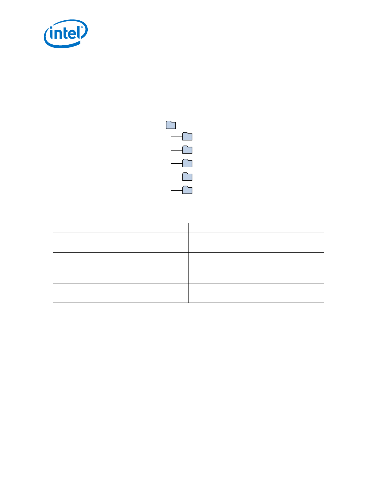
1. Download the development kit installer from the Stratix 10 GX Transceiver Signal
documents
board_design_files
examples
factory_recovery
demos
<package rootdir>
Integrity Development Kit link on the Intel website.
2. Unzip the Intel Stratix 10 Transceiver Signal Integrity Development Kit installer
package.
3. The installer package creates the development kit directory structure shown in the
figure below.
Figure 1. Development Kit Directory Structure
The table below lists the file directory names and a description of their contents
2 Getting Started
Table 1. Installed Development Kit Directory Structure
File Directory Name Description of Directory Contents
board_design_files
demos
documents
examples
factory_recovery
Contains schematics, layout, assembly and bill of material
board design files. Use these files as a starting point for a
new prototype board design
Contains demonstration applications when available
Contains the development kit documentation
Contains the sample design files for the development kit
Contains the original data programmed onto the board
before shipment. Use this data to restore the board with its
original factory contents.
2.3 Installing the Intel FPGA Download Cable Driver
The Intel Stratix 10 GX Transceiver Signal Integrity Development Kit includes
embedded Intel FPGA Download Cable circuits for FPGA and MAX® V programming.
However, for the host computer and board to communicate, you must install the Intel
FPGA Download Cable driver on the host computer.
Installation instructions for the Intel FPGA Download Cable driver for your operating
system are available on the Intel website.
On the Intel website, navigate to the Cable and Adapter Drivers Information link to
locate the table entry for your configuration and click the link to access the
instructions.
Intel® Stratix® 10 GX Transceiver Signal Integrity Development Kit User Guide
6
Page 7

3 Development Board Setup
3 Development Board Setup
The instructions in this chapter explain how to setup the Intel Stratix 10 GX
Transceiver Signal Integrity Development Board.
3.1 Setting up the Development Board
To prepare and apply power to the board, perform the following steps:
1. The Intel Stratix 10 GX transceiver signal integrity development kit ships with its
board switches preconfigured to support the design examples in the kit. If you
suspect your board might not be correctly configured with the default settings,
follow the instructions in the Factory Default Switch and Jumper Settings on page
8 to return the board to its factory settings before proceeding.
2. The development kit ships with design examples stored in the flash device. The
POWER-ON slide switch (SW7) is provided to turn the board ON or OFF.
Caution: When the power cord is plugged into connector J103 of the Intel Stratix
10 transceiver signal integrity development kit, 12V_IN and 3.3V_STBY
are present on to the board with switch SW7 in the 'OFF' position.
These voltages are restricted to a small area of the board. When switch
SW7 is placed to 'ON' position, all voltages planes have power at this
point.
3.
Set the POWER-ON switch SW7 to the ON position. When power is supplied to the
board, three green LEDs (D29, D31 and D32) illuminate and an amber LED
(D36) extinguishes indicating that the board has power. If the amber LED (D36)
illuminates, it indicates that one or more power supply is incorrect.
4.
RESET button (S12) is connected to the MAX V CPLD (MAX_RESETn pin) that is
used for AvST configuration. When this button is pressed, the MAX V CPLD
initiates a reloading of the stored image from the flash memory using AvST
configuration mode. The image loaded right after power cycle or MAX V reset
depends on FACTORY_LOAD settings.
• OFF(1) - factory load
• ON (0) - user defined load #1
Page selection can be changed by the PGMSEL button (S10) when the board is
powered on, and PGM_CONFIG (S11) is used to reconfigure FPGA with
corresponding page which is indicated by PGM_LED0, PGM_LED1 or PGM_LED2.
Caution: Use only the supplied power supply. Power regulation circuits on the
board can get damaged by power supplies with greater voltage.
The MAX V CPLD device on the board contains a parallel flash loader II (PFL II)
megafunction. After a POWER-ON or RESET (reconfiguration) event, the MAX V CPLD
configures the Intel Stratix 10 FPGA in AvST mode with either factory design or user
design depending on the setting of FACTORY_LOAD.
Intel Corporation. All rights reserved. Intel, the Intel logo, Altera, Arria, Cyclone, Enpirion, MAX, Nios, Quartus
and Stratix words and logos are trademarks of Intel Corporation or its subsidiaries in the U.S. and/or other
countries. Intel warrants performance of its FPGA and semiconductor products to current specifications in
accordance with Intel's standard warranty, but reserves the right to make changes to any products and services
at any time without notice. Intel assumes no responsibility or liability arising out of the application or use of any
information, product, or service described herein except as expressly agreed to in writing by Intel. Intel
customers are advised to obtain the latest version of device specifications before relying on any published
information and before placing orders for products or services.
*Other names and brands may be claimed as the property of others.
ISO
9001:2008
Registered
Page 8
3 Development Board Setup
The development kit includes a MAX V CPLD design which contains the PFL II
megafunction. The design resides in the <package dir>\examples\max5 directory.
When configuration is complete, LED D25 (CONF_DONE) illumintes signaling that the
Intel Stratix 10 GX FPGA device is configured successfully. If the configuration fails,
the LED D23 (ERROR) illuminates.
3.2 Factory Default Switch and Jumper Settings
This section shows the factory switch settings for the Intel Stratix 10 GX transceiver
signal integrity development kit.
Table 2. Factory Default Switch Settings
Switch Board Label Default Position Function
SW10
MSEL2
MSEL1
SW11
SW3-1 Intel Stratix 10 OPEN/OFF Enable Intel Stratix 10 in
SW3-2
SW3-3
SW3-4
S15-1
S15-2
SW1-1
SW1-2
SW1-3
SW1-4
SW2-1
SW2-2
S1-1
S1-2
S14-1
S14-2
SW9-1
SW9-2
MSEL0
MAX V
FMC A
FMC B
OFF = OSC
ON = SMA
S0
S1
SS0
SS1
OFF=ISOLATE
ON=FULL CHAIN
OFF=ISOLATE
ON=FULL CHAIN
VCCT
VCCH
VCCRR
VCCRL
2-3 Closed MSEL setting=0
5-6 Closed MSEL setting=0
2-3 Closed MSEL setting=0
JTAG Chain
OPEN/OFF Enable MAX V in JTAG chain
CLOSE/ON Bypass FMC A in JTAG chain
CLOSE/ON Bypass FMC B in JTAG chain
OPEN/OFF Select Si570 clock source for
OPEN/OFF Select Si570 clock source for
OPEN/OFF Frequency Select
CLOSE/ON Frequency Select
OPEN/OFF Spread Spectrum Select
OPEN/OFF Spread Spectrum Select
CLOSE/ON U15 (LTC2987) is enabled in
CLOSE/ON U15 (LTC2987) is enabled in
CLOSE/ON U5 and U6 (Si5341) is
CLOSE/ON U5 and U6 (Si5341) is
OPEN/OFF
OPEN/OFF
OPEN/OFF
OPEN/OFF
U3
U4
I2C topology
I2C topology
enabled in I2C topology
enabled in I2C topology
Enable on-board VCCT
regulator
Enable on-board VCCH
regulator
Enable on-board VCCRR
regulator
Enable on-board VCCRL
regulator
continued...
Intel® Stratix® 10 GX Transceiver Signal Integrity Development Kit User Guide
8
Page 9
3 Development Board Setup
Switch Board Label Default Position Function
SW9-3
SW9-4
SW8-1
SW8-2
SW8-3
SW8-4
SW6-1
SW6-2
SW6-3
SW6-4
SW4-1
SW4-2
SW4-3
SW4-4
SW5-1
SW5-2
SW5-3
SW5-4
SW7
VCCERAM
VCC
MAX10_DIPSWITCH
FAN_ON
PWR_MGMT_SEL
MAX10_BOOTSEL
FACTORY_LOAD
MAX5_SWITCH2
MAX5_SWITCH0
MAX5_SWITCH1
S10_UNLOCK
USER_DIP6
USER_DIP5
USER_DIP4
USER_DIP3
USER_DIP2
USER_DIP1
USER_DIP0
SW7
OPEN/OFF
OPEN/OFF
OPEN/OFF Power Intel MAX 10 user DIP
OPEN/OFF FAN is not full speed
OPEN/OFF Select Linear Tech PWR
OPEN/OFF Power Intel MAX 10 boot
OPEN/OFF Factory Load Control
OPEN/OFF MAX V user DIPSwitch
OPEN/OFF MAX V user DIPSwitch
OPEN/OFF MAX V user DIPSwitch
OPEN/OFF Stratix 10 User DIPSwitch
OPEN/OFF Stratix 10 User DIPSwitch
OPEN/OFF Stratix 10 User DIPSwitch
OPEN/OFF Stratix 10 User DIPSwitch
OPEN/OFF Stratix 10 User DIPSwitch
OPEN/OFF Stratix 10 User DIPSwitch
OPEN/OFF Stratix 10 User DIPSwitch
OPEN/OFF Stratix 10 User DIPSwitch
OFF On-board power switch
Enable on-board VCCERAM
regulator
Enable on-board VCC
regulator
Switch
MGMT solution
select
Intel® Stratix® 10 GX Transceiver Signal Integrity Development Kit User Guide
9
Page 10
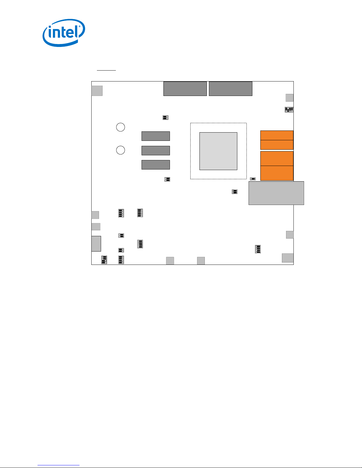
Figure 2. Default Switch Settings
Board size = 10" x11"
1 inch
S10GX
UF50
J28
QSFP 28 1
J27
QSFP 28 0
J30
SFP + 1
FMC+ A
J58
FMC+ B
J59
J14
CN1
J19
CFP4
J24
J29
SFP + 0
J92
J94
S15
S1
SW3
SW9
S14
SW8
VCCRR
SW6
ON
ON
ON
ON
ON
ON
ON
SW5
ON
SW4
ON
J89
J79 J91
VCCERAM
VCCT
VCCH
Bottom
Layer
J83
VCCRL
J86
SW2
Ethernet
Ext.
JTAG
USB
VCC
GND
ON
ON
SW7
MXP-0 J33
MXP-1 J44
MXP-2 J50
SW1
ON
SW10
0
1
SW11
0
1
3 Development Board Setup
Intel® Stratix® 10 GX Transceiver Signal Integrity Development Kit User Guide
10
Page 11
ENET FPGA (SGMII)
Buttons, Switches,
LEDs, GPIOs
LCD
MXP Transceiver
2.4 mm Transceiver
SFP+ x2
QSFP28 x2
CFP4
EPCQ-L
32 bit CFI Flash
FMC-B x16FMC-A V57.1/V57.4
Intel Stratix 10 FPGA
ND5 F2397B Package
1SG280UF50
LVDS X80 Pairs
CLKIN X6 Pairs
REFCLK X2 Pairs
Transceiver X24 Ch
LVDS X34 Pairs
CLKIN X4 Pairs
Transceiver X16 Ch
MAX 10 FPGA
On-Board USB
Blaster II
and USB Interface
Side Bus
JTAG Chain
USB Type-B
LVDS X2 Pairs
X2
Transciever X12 Ch
Transciever X6 Ch
Transciever X2 Ch
Transciever X8 Ch
Transciever X4 Ch
AS X4
Transciever X6 Ch
MAX V
CPLD
PLLs
Programmable
Oscillators
SMA Clock
IN/OUT
CLK
CLKIN
CLKIN
Avalon-ST X32
X67
I2C
MAX 10 Power
Management
(Backup)
LT Power
Management
VCC
VCCERAM
VCCT
VCCR
VCCH
VCCIO
4 Board Components
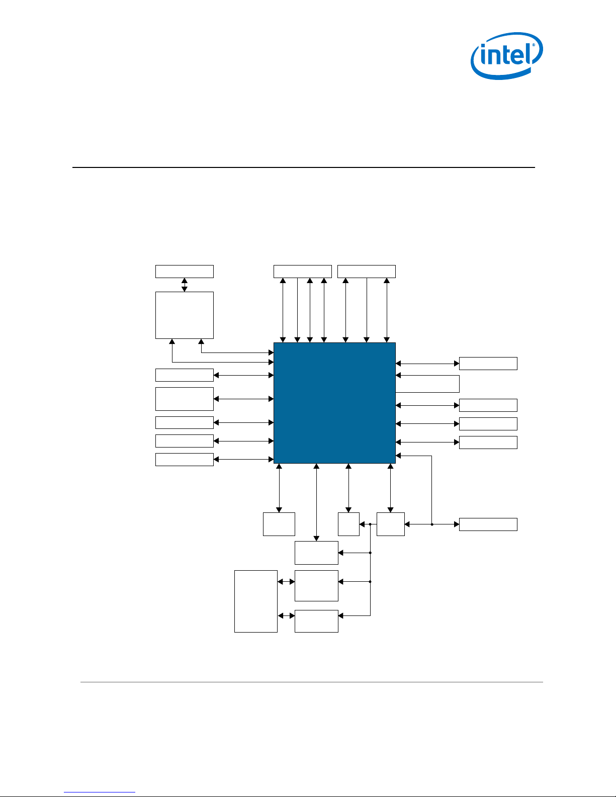
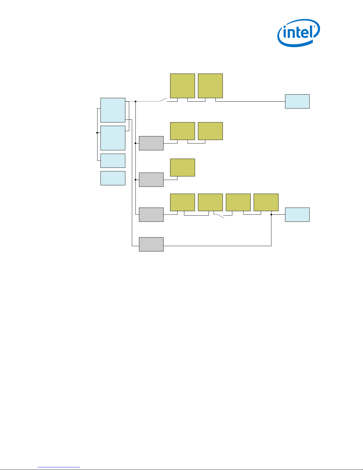
4 Board Components
4.1 Board Overview
This section provides an overview of the Intel Stratix 10 GX transceiver signal integrity
development board including a block diagram of the board.
Figure 3. Stratix 10 GX Transceiver Signal Integrity Development Kit User Guide Block
Diagram
Intel Corporation. All rights reserved. Intel, the Intel logo, Altera, Arria, Cyclone, Enpirion, MAX, Nios, Quartus
and Stratix words and logos are trademarks of Intel Corporation or its subsidiaries in the U.S. and/or other
countries. Intel warrants performance of its FPGA and semiconductor products to current specifications in
accordance with Intel's standard warranty, but reserves the right to make changes to any products and services
at any time without notice. Intel assumes no responsibility or liability arising out of the application or use of any
information, product, or service described herein except as expressly agreed to in writing by Intel. Intel
customers are advised to obtain the latest version of device specifications before relying on any published
information and before placing orders for products or services.
*Other names and brands may be claimed as the property of others.
ISO
9001:2008
Registered
Page 12
4 Board Components
Intel Stratix 10 GX Transceiver Signal Integrity Development Board
Components
Table 3. Board Components Table
Board Reference Type Description
Featured Devices
U43 FPGA Intel Stratix 10 GX 280 F2397 FPGA
U20 CPLD System MAX V CPLD (5M2210ZF256)
U97 FPGA USB Intel MAX 10 FPGA
U98 FPGA PWR Intel MAX 10 FPGA
General User Input and Output
D12-D19 User LEDs (Green) User LEDs (Green)
D20-D25 MAX V LEDs (Green) MAX V LEDs (Green)
S2-S13 User Push Buttons User Push Buttons
SW4-SW5 User DIP Switches User DIP
SW6 MAX V DIP Switch MAX V DIP Switch
J20 LCD Display Header Connector for 16 Character x2 line LCD
Configuration, Status and Setup Elements
J14 Intel FPGA Download Cable
Programming Header
D1-D2 Green LEDs JTAG Transmit-Receive Activity
D3-D4 Green LEDs System Console Transmit-Receive
D36 Amber LEDs System Power error indicator
D5-D6 Green LEDs FMC cards present indicator
D7-D11 Ethernet LEDs Ethernet LEDs (TX/RX/LINK)
Clock Circuits
X2
50-MHz Oscillator
X1 This 50-MHz oscillator provides clock to
SW1 Spread Spectrum/Frequency Selection
Switch
Y1
Transceiver Dedicated Reference Clock/
Programmable Oscillator
(10M04SCU169)
(10M16SAU169)
Header to interface external Intel FPGA
Download Cable direct to FPGA
(through USB Intel MAX 10)
Activity
This 50-MHz oscillator is the clock
source to clock buffer SL18860DC that
provides three 50 MHz outputs to the
FPGA and the MAX V CPLD
the PWR Intel MAX 10 FPGA
SW1 selects frequency and spread
spectrum percentages of clock buffer
outputs ICS557-03.
Feeds REFCLKs on left side of the Intel
Stratix 10 GX FPGA device and an
LVDS trigger output at board reference
J4/J5.
The external input is available at board
reference J2 and J3. The default
frequency is 644.53125 MHz.
continued...
Intel® Stratix® 10 GX Transceiver Signal Integrity Development Kit User Guide
12
Page 13
4 Board Components
Board Reference Type Description
Y2
U3, U4, U5
Transceiver Dedicated Reference Clock/
U6
J61, J63 External core clock input
J62, J64 External core clock output SMA external output at
Programmable PLL
Feeds REFCLKs on right side of the
Intel Stratix 10 GX FPGA device and an
LVDS trigger output at board reference
J8/J9.
The external input is available at board
reference J6 and J7. The default
frequency is 706.25 MHz.
Feeds REFCLKs on left side of the Intel
Stratix 10 GX FPGA device and an
LVDS trigger output at board reference
J10/J11.
The default frequencies are 625 MHz,
614.4 MHz, 100 MHz.
Feeds REFCLKs on right side of the
Intel Stratix 10 GX FPGA device and an
LVDS trigger output at board reference
J12/J13.
The default frequencies are 625 MHz,
644.53125 MHz, 125 MHz.
SMA external input at CLKIN_3C0
PLL_3C_CLKOUT0
J65-J66
J67-J68 SMA external input bank at 1M
J69-J70 SMA external input bank at 4C
J71-J72 SMA external input bank at 4K
X4 100-MHz Oscillator This 100-MHz oscillator provides clock
J33, J44, J50 MXP connector 17 Gbps/28 Gbps, 4 channels MXP
J31-J32
J34-J43
J45-J49
J51-J57
J29-J30 SFP+ optical transceiver interface 17 Gbps/28 Gbps, 2 channels
J27-J28 QSFP28 optical transceiver interface 17 Gbps/28 Gbps, 8 channels
J24 CFP4 optical transceiver interface 17 Gbps/ 28 Gbps, 4 channels
J58-J59 FMC+ connector 17 Gbps/28 Gbps, 34 channels
U21-U22 Flash Memory Two 1-Gbit Micron PC28F00AP30BF CFI
External transceiver clock input
Transceiver Interfaces
2.4 mm RF connector 17 Gbps/ 28 Gbps, 6 channels 2.4 mm
Memory Devices
Communication Ports
SMA external input bank at 1C
to the MAX V CPLD
connectors
RF connectors
connected to SFP+ modules
connected to QSFP28 modules
connected to CFP4 module
connected to FMC+ connectors
Flash device
continued...
Intel® Stratix® 10 GX Transceiver Signal Integrity Development Kit User Guide
13
Page 14
4 Board Components
Board Reference Type Description
J19 Gigabit Ethernet Port RJ-45 connector which provides a
CN1 USB Type-B connector Connects a type-B USB cable
Power Supply
U15 LTM2987 Linear Technology power monitor
U63-U64
U66-U67
U68 LTM4620
U69 LTM4620
U70 LTM4620
U71 LTM4620
U74 EN63A0
U78 EN63A0
U79 EN6337
U82 LTM4630A
LTM4677
3x LTM4650
10/100/1000 Ethernet connection
through a Marvell 88E1111 PHY
device
Power regulators for VCC rail
Power regulators for VCCERAM rail
Power regulators for VCCH rail
Power regulators for VCCRL rail
Power regulators for VCCRR rail
Power regulators for FMCA_VADJ rail
Power regulators for FMCB_VADJ rail
Power regulators for 2.5V rail
Power regulators for 3.3V rail
4.2 Stratix 10 GX FPGA
The development board features the Intel Stratix 10 GX FPGA (1SG280UF50).
Intel Stratix 10 GX FPGA I/O Usage Summary
Table 4. Stratix 10 GX FPGA Pin Table
Signal Name/Function I/O Count Description
S10_JTAG_TCK/TDO/TDI/TMS
FPGA_MSEL[2:0]
FPGA_CONF_DONE
FPGA_nSTATUS
FPGA_INIT_DONE
FPGAMSEL0
FPGA_nCONFIG
FPGA_OSC_CLK_1
FPGA_AS_CLK
CPU_RESETn
4 JTAG Configuration Pins
2 Configuration input pins to set
1 Configuration done pin
1 Configuration status pin
1 Configuration pin to signify user mode
1 Configuration input pins to set
1 Configuration input pin to reset FPGA
1 125 MHz Clock
1 Configuration Clock for AS
1 Global reset signal
Configuration
configuration scheme
configuration scheme and Chip select
pin to EPCQL device
configuration schemes
continued...
Intel® Stratix® 10 GX Transceiver Signal Integrity Development Kit User Guide
14
Page 15

4 Board Components
Signal Name/Function I/O Count Description
FPGA_CONFIG_D[31:0]
FPGA_AS_DATA[3:0]
FPGA_AVST_READY
FPGA_AVST_VALID
FPGA_AVST_CLK
FPGA_PR_DONE
FPGA_PR_REQUEST
FPGA_PR_ERROR
NPERSTL, NPERSTR
FPGA_SDM10
FPGA_CvP_DONE
FPGA_SEU_ERR
VCC_SDA/VCC_SCL
VCC_ALERTn
SFP0_TX_DS
SFP0_RS[1:0]
SFP0_MOD_ABS
SFP0_RX_LOS
SFP0_TX_FLT
SFP0_SCL
SFP0_SDA
SFP1_TX_DIS
SFP1_RS[1:0]
SFP1_MOD_ABS
SFP1_RX_LOS
SFP1_TX_FLT
SFP1_SCL
SFP1_SDA
CFP4_MOD_LOPWR
CFP4_MOD_RSTn
CFP4_GLB_ALRMN
32 Configuration input pin that enables all
IOs
4 EPCQL data bus
1 SDM ready for AvST configuration
scheme
1 Data valid for AvST configuration
scheme
1 Configuration clock for AvST
configuration scheme
1 Partial reconfiguration done pin
1 Partial reconfiguration request pin
1 Partial reconfiguration error pin
4 Reset pin for PCIe HIP
1 SDM IO 10
1 CvP configuration done pin
1 SEU error indicate pin
2 SmartVID PMBus
1 SmartVID PMBus
Transceivers
1 SFP+ 0 TX disable control Pin
2 SFP+ 0 Rate Select Control Pin
1 SFP+ 0 Module Absent Status Pin
1 SFP+ 0
1 SFP+ 0 Transmitter Fault Status Pin
1 SFP+ 0 Management Data Clock
1 SFP+ 0 Management Data I/O Bi-
Directional Data
1 SFP+ 1 TX disable control pin
2 SFP+ 1 Rate Select Control Pin
1 SFP+ 1 Module Absent Status Pin
1 SFP+ 1
1 SFP+ 1 Transmitter Fault Status Pin
1 SFP+ 1 Management Data Clock
1 SFP+ 1 Management Data I/O Bi-
Directional Data
1 CFP4 Module Low Power Mode
1 CFP4 Module Reset
1 CFP4 Program Alarm bits
continued...
Intel® Stratix® 10 GX Transceiver Signal Integrity Development Kit User Guide
15
Page 16
Signal Name/Function I/O Count Description
CFP4_PRTADR[2:0]
CFP4_TX_DIS
CFP4_RX_LOS
CFP4_MOD_ABS
CFP4_MDC
CFP4_MDIO
eQSFP_modselL0
eQSFP_resetL0
eQSFP_LPmode0
eQSFP_modprsL0
eQSFP_intl0
eQSFP_scl0
eQSFP_sda0
eQSFP_modselL1
eQSFP_resetL1
eQSFP_LPmode1
eQSFP_modprsL1
eQSFP_intl1
eQSFP_scl1
eQSFP_sda1
FALAp/n[33:0]
FAHAp/n[23:0]
FAHBp/n[21:0]
RZQ_2M
RZQ_3K
EXTA_SDA1V8
EXTA_SCL1V8
FAPRSNT1V8_N
FACLKBIR1V8
FBLAp/n[33:0]
EXTB_SDA1V8
EXTB_SCL1V8
FBPRSTN1V8_N
3 CFP4 MDIO Physical Port Address
1 CFP4 Transmitter Disable
1 CFP4 Receiver loss of signal
1 CFP4 Module Absent
1 CFP4 Management Data Clock
1 CFP4 Management Data I/O Bi-
Directional Data
1 QSFP28 0 model select
1 QSFP28 0 Module Reset
1 QSFP28 0 Module Low Power Mode
1 QSFP28 0 Module Present
1 QSFP28 0 Module Interrupt
1 QSFP28 0 Management Data Clock
1 QSFP28 0 Management Data I/O Bi-
Directional Data
1 QSFP28 1 model select
1 QSFP28 1 Module Reset
1 QSFP28 1 Module Low Power Mode
1 QSFP28 1 Module Present
1 QSFP28 1 Module Interrupt
1 QSFP28 1 Management Data Clock
1 QSFP28 1 Management Data I/O Bi-
Directional Data
68 FMC A LA bank GPIOs
48 FMC A HA bank GPIOs
44 FMC A HB bank GPIOs
1 RZQ pin for bank 2M
1 RZQ pin for bank 3K
1 FMC A I2C bus
1 FMC A I2C bus
1 FMC A present indicator
1 FMC A clock direction control
68 FMC B LA bank GPIOs
1 FMC B I2C bus
1 FMC I2C bus
1 FMC B present indicator
4 Board Components
continued...
Intel® Stratix® 10 GX Transceiver Signal Integrity Development Kit User Guide
16
Page 17
4 Board Components
Signal Name/Function I/O Count Description
USB_FULL
USB_EMPTY
USB_RESETn
USB_OEn
USB_RDn
USB_WRn
USB_DATA[7:0]
USB_ADDR[1:0]
USB_SCL
USB_SDA
FM_D[31:0]
FM_A[26:1]
FLASH_WEn
FLASH_CEn0
FLASH_CEn1
FLASH_OEn
FLASH_RDYBSYn0
FLASH_RDYBSYn1
FLASH_RESETn
FLASH_CLK
FLASH_ADVn
MAX5_OEn
MAX5_CSn
MAX5_WEn
MAX5_CLK
MAX5_BEn[3:0]
USER_LED[7:0]
USER_PB[7:0]
USER_DIP[6:0]
USER_IO[9:0]
USB
1 USB FIFO is full
1 USB FIFO is empty
1 USB Reset
1 USB Output Enable
1 USB Read
1 USB Write
8 USB Data Bus
2 USB Address Bus
1 USB Serial Clock
1 USB Serial Data
Flash Memory
32 Flash Data Bus
26 Flash Address Bus
1 Flash Write Enable Strobe
1 Flash Chip Enable
1 Flash Chip Enable
1 Flash Output Enable
1 Flash ready or busy
1 Flash ready or busy
1 Flash reset
1 Flash clock
1 Flash address valid
MAX V CPLD
1 Output Enable
1 Chip Select
1 Write Enable
1 Clock
4 Byte Enable
Switches, Buttons, LED
8 Light Emitting Diodes
8 Push Buttons
7 DIP Switches
10 Input/Output
continued...
Intel® Stratix® 10 GX Transceiver Signal Integrity Development Kit User Guide
17
Page 18
Signal Name/Function I/O Count Description
S10_UNLOCK
ENET_SGMII_TX_P/N
ENET_SGMII_RX_P/N
ENET_RSTn
ENET_INTn
ENET_MDIO
ENET_MDC
SPARE[20:1]
I2C_1V8_SCL
I2C_1V8_SDA
OVERTEMPn
TEMP_ALERTn
CLK_50M_S10
CLK_S10BOT_100M_p/n
CLKIN_SMA_3C_p/n
CLKOUT_SMA_3C_p/n
USB_FPGA_CLK
CLK_S10TOP_ADJ_p/n
CLK_S10TOP_125M_p/n
FACLKM2Cp/n0
FACLKM2Cp/n1
FBCLKM2Cp/n0
FBCLKM2Cp/n1
FACLKBIDIRp/n2
FACLKBIDIRp/n3
1 FPGA Unlock Switch
Ethernet
2 Ethernet SGMII Transmit Data
2 Ethernet SGMII Receive Data
1 Reset
1 Interrupt
1 Ethernet Management Data I/O
1 Ethernet Management Data Clock
Other Bus
20 Spare bus between Intel Stratix 10 and
MAX V
1 Intel Stratix 10 I2C bus
1 Intel Stratix 10 I2C bus
Temperature
1 Intel Stratix 10 over temperature
indicator
1 Intel Stratix 10 temperature alert
indicator
Global Clocks
1 50 MHz Global Clock Input
2 100 MHz differential core clock for
bottom banks
2 Global Clock input from SMA
2 Dedicated Clock output to SMA
1 USB FPGA Clock
2 Adjustable differential core clock for
top banks
2 125 MHz differential core clock for top
banks
2 FMC A clock input 0
2 FMC A clock input 1
2 FMC B clock input 0
2 FMC B clock input 1
2 FMC A bidirectional clock 2
2 FMC A bidirectional clock 3
Transceiver Clocks
4 Board Components
continued...
Intel® Stratix® 10 GX Transceiver Signal Integrity Development Kit User Guide
18
Page 19
4 Board Components
Signal Name/Function I/O Count Description
CLK_CFP4_644_p/n
CLKIN_SMA_1C_p/n
CLK_QSFP0_644MT_p/n
CLK_QSFP0_644MB_p/n
CLK_GXBL1E_614MT_p/n
CLK_GXBL1E_614MB_p/n
CLK_GXBL1F_625M_p/n
CLK_SFP_644M_p/n
CLK_GXBL1K_614M_p/n
CLK_GXBK1L_625M_p/n
FBGBTCLKM2_Cp/n0
CLKIN_SMA_1M_p/n
CLK_FMCB_644M_p/n
FBGBTCLKM2_Cp/n1
CLK_SMA_706M_p/n
CLKIN_SMA_4C_p/n
CLK_MXP1_706M_p/n
CLK_GXBR4D_644M_p/n
CLK_MXP2_706M_p/n
CLK_GXBR4E_644M_p/n
CLK_MXP3_706M_p/n
CLK_GXB4F_644M_p/n
FAGBTCLKM2_Cp/n0
2
2
2
2
2
2
2
2
2
2
2
2
2
2
2
2
2
2
2
2
2
2
2
Differential top REFCLK input to the
transceiver bank 1C
Differential bottom REFCLK input to
the transceiver bank 1C
Differential top REFCLK input to the
transceiver bank 1D
Differential bottomREFCLK input to the
transceiver bank 1D
Differential top REFCLK input to the
transceiver bank 1E
Differential bottom REFCLK input to
the transceiver bank 1E
Differential top REFCLK input to the
transceiver bank 1F
Differential top REFCLK input to the
transceiver bank 1K
Differential bottom REFCLK input to
the transceiver bank 1K
Differential top REFCLK input to the
transceiver bank 1L
Differential top REFCLK input to the
transceiver bank 1M
Differential bottomREFCLK input to the
transceiver bank 1M
Differential top REFCLK input to the
transceiver bank 1N
Differential bottom REFCLK input to
the transceiver bank 1N
Differential top REFCLK input to the
transceiver bank 4C
Differential bottomREFCLK input to the
transceiver bank 4C
Differential top REFCLK input to the
transceiver bank 4D
Differential bottom REFCLK input to
the transceiver bank 4D
Differential top REFCLK input to the
transceiver bank 4E
Differential bottom REFCLK input to
the transceiver bank 4E
Differential top REFCLK input to the
transceiver bank 4F
Differential bottomREFCLK input to the
transceiver bank 4F
Differential top REFCLK input to the
transceiver bank 4K
continued...
Intel® Stratix® 10 GX Transceiver Signal Integrity Development Kit User Guide
19
Page 20
Signal Name/Function I/O Count Description
CLKIN_SMA_4K_p/n
FAGBTCLKM2_Cp/n1
CLK_GXBR4L_644M_p/n
FAGBTCLKM2_Cp/n2
CLK_GXBR4M_625M_p/n
FAGBTCLKM2_Cp/n3
CLK_FMCA_706M_p/n
2
2
2
2
2
2
2
4.3 MAX V CPLD System Controller
The Intel Stratix 10 GX transceiver signal integrity development kit consists of a MAX
V CPLD (5M2210Z-F256), 256-pin FineLine BGA package. MAX V CPLD devices provide
programmable solutions for applications such as FPGA reconfiguration from flash
memory, I2C chain to manage power consumption, core temperature, fan speed, clock
frequency and remote update system. MAX V devices feature on-chip flash storage,
internal oscillator and memory functionality. With up to 50% lower total power versus
other CPLDs and requiring as few as one power supply, MAX V CPLDs can help you
meet your low power design requirements.
4 Board Components
Differential bottom REFCLK input to
the transceiver bank 4K
Differential top REFCLK input to the
transceiver bank 4L
Differential bottom REFCLK input to
the transceiver bank 4L
Differential top REFCLK input to the
transceiver bank 4M
Differential bottomREFCLK input to the
transceiver bank 4M
Differential top REFCLK input to the
transceiver bank 4N
Differential bottomREFCLK input to the
transceiver bank 4N
The following list summarizes the features of MAX V CPLD devices:
• 2210 Logic Elements (LEs)
• 8192 bits of User Flash Memory
• 4 global clocks
• 1 internal oscillator
• 271 maximum user I/O pins
• Low-cost, low power and non-volatile CPLD architecture
• Fast propagation delays and clock-to-output times
• Single 1.8V external supply for device core
• Bus-friendly architecture including programmable slew rate, drive strength, bushold and programmable pull-up resistors
The table below lists the MAX V CPLD I/O signals.
Table 5. MAX V CPLD I/O Signals
Signal Name Description
FA_A[26:1]
FM_D[31:0]
Flash Address Bus
Flash Data Bus
continued...
Intel® Stratix® 10 GX Transceiver Signal Integrity Development Kit User Guide
20
Page 21
4 Board Components
FLASH_CLK
FLASH_RESETn
FLASH_CEn[1:0]
FLASH_OEn
FLASH_WEn
FLASH_ADVn
FLASH_RDYBSYn[1:0]
FPGA_CONFIG_D[31:0]
FPGA_INIT_DONE
FPGA_nSTATUS
FPGA_CONF_DONE
FPGA_nCONFIG
FPGA_ASCLK
FPGA_SEU_ERR
FPGA_CvP_DONE
FPGA_SDM
FPGA_PR_REQUEST
FPGA_PR_DONE
FPGA_PR_ERROR
FPGA_MSEL[2:0]
FPGA_AVST_CLK
FPGA_AVST_VALID
FPGA_AVST_READY
I2C_1V8_SCL
I2C_1V8_SDA
FAPRSNT1V8_N
FBPRSNT1V8_N
SI5341_1_ENn
SI5341_1_INTn
SI5341_1_RSTn
SI5341_1_LOLn
SI5341_2_ENn
SI5341_2_INTn
SI5341_2_RSTn
Signal Name Description
Flash Clock
Flash Reset
Flash Chip Enable
Flash Output Enable
Flash Write Enable
Flash Address Valid
Flash Chip Ready/Busy
FPGA AvST configuration data bus
FPGA initialization complete
FPGA status
FPGA configuration complete
FPGA configuration control pin reset to FPGA
FPGA AS configuration clock
FPGA configuration SEU error
FPGA CvP configuration done
FPGA SDM IO10
FPGA partial reconfiguration request
FPGA partial reconfiguration done
FPGA partial reconfiguration error
FPGA configuration mode setting bits
FPGA AvST configuration clock
FPGA AvST configuration data valid
FPGA ready to receive data
MAX V I2C bus
MAX V I2C bus
FMC A present indicator
FMC B present indicator
SI5341 1 ENABLE
SI5341 1 interrupt indicators
SI5341 1 reset
SI5341 1 loss of clock indicators
SI5341 2 ENABLE
SI5341 2 interrupt indicators
SI5341 2 reset
continued...
Intel® Stratix® 10 GX Transceiver Signal Integrity Development Kit User Guide
21
Page 22
SI5341_2_LOLn
EN_MASTER[1:0]
TEMP_ALERTn
OVERTEMPn
OVERTEMP
FAN_RPM
USB_CFG[14:0]
USB_MAX5_CLK
MAX_OSC_CLK_1
MAX5_JTAG_TCK
MAX5_JTAG_TMS
MAX5_JTAG_TDI
MAX5_JTAG_TDO
FACTORY_LOAD
MAX5_SWITCH [2:0]
PGM_SEL
PGM_CONFIG
MAX_RESETn
CPU_RESETn
PGM_LED[2:0]
MAXV_ERROR
MAXV_LOAD
MAXV_CONF_DONE
MAX5_BE_n[3:0]
MAX5_OEn
MAX5_CSn
MAX5_WEn
MAX5_CLK
SPARE[20:1]
CLK_50M_MAX5
FPGA_ASDATA[3:0]
CLK_CONFIG
4 Board Components
Signal Name Description
SI5341 2 loss of clock indicators
ENABLE specific I2C buffer
FPGA temperature alert input
FPGA over temperature input
Over temperature fan control
Fan speed control
Bus between USB Intel MAX 10 and MAX V
Clock from USB PHY chip
25MHz / 100 MHz / 125 MHz clock input
MAX V Test Clock
MAX V Test Mode Select
MAX V Test Data Input
MAX V Test Data Output
Factory image for configuration
System MAX V user DIP switch
Flash Memory program select pushbutton
Flash Memory program configuration pushbutton
System MAX V reset pushbutton
CPU reset pushbutton
Flash image program select indicators
Intel Stratix 10 configuration error indicator LED
Intel Stratix 10 configuration active indicator LED
Intel Stratix 10 configuration done indicator LED
Intel Stratix 10 and MAX V data path, byte enable
Intel Stratix 10 and MAX V data path, output enable
Intel Stratix 10 and MAX V data path, chip select
Intel Stratix 10 and MAX V data path, write enable
Intel Stratix 10 and MAX V data path, clock
Spare bus between MAX V and Intel Stratix 10
50 MHz clock input
Intel Stratix 10 AS configuration data
100 MHz clock input
Intel® Stratix® 10 GX Transceiver Signal Integrity Development Kit User Guide
22
Page 23
Intel
Stratix 10
U43
MAX V
U20
MAX II USB
U97
USB-PHY
U9
I2C Buffer
U26
I2C Buffer
U28
I2C Buffer
U27
I2C Buffer
U29
Si5341
PLL
(1.8 V)
Si5341
PLL
(1.8 V)
add = 74h add = 76h
Si570 OSC
(2.5 V)
Si570 OSC
(2.5 V)
add = 66h add = 77h
(1.8 to 2.5 V)
(1.8 to 5 V)
(1.8 to 3.3 V)
(1.8 to 3.3 V)
Si570 OSC
(2.5 V)
add = 66h
MAX 10
FPGA
MAX 1619
add = 5Eh add = 18h
LTM2987
PM0/1
LTM4677
add = 5C/5Dh add = 4Fh
add = 31h/5Ah
add = 5Bh
J102 Silab
Debug Cable
J17 LT
Debug Cable
net name = VCC_SCL
net name = I2C_1V8_SCL
S1
net name = I2C_1V8_SCL_Si5341
net name = I2C_2V5_SCL
net name = I2C_5V_SCL
net name = I2C_3V3_SCL
SW2
net name =LT_SCL
4 Board Components
Figure 4. I2C Block Diagram
4.4 FPGA Configuration
This section describes the FPGA, flash memory and MAX V CPLD System Controller
device programming methods supported by the Intel Stratix 10 GX tranceiver signal
integrity development kit.
Three configuration methods except AS mode are mostly used on the Intel Stratix 10
transceiver signal integrity development kit.
• Embedded USB-Blaster is the default method for configuring the FPGA at any time
• MAX V configures the FPGA device via AvST mode using stored images from CFI
4.4.1 FPGA Programming over Embedded USB-Blaster
• JTAG external header for debugging. Intel recommends that you use lower JTAG
Embedded USB-Blaster is the default method for configuring the Intel Stratix 10 GX
FPGA using the Intel Quartus Prime Programmer in the JTAG mode with the supplied
USB cable.
using the Intel Quartus Prime Programmer in JTAG mode with the supplied USB
cable.
flash devices either at power-up or pressing the MAX_RESETn/PGM_CONFIG push
button.
clock frequency value such as 16 MHz.
Intel® Stratix® 10 GX Transceiver Signal Integrity Development Kit User Guide
23
Page 24
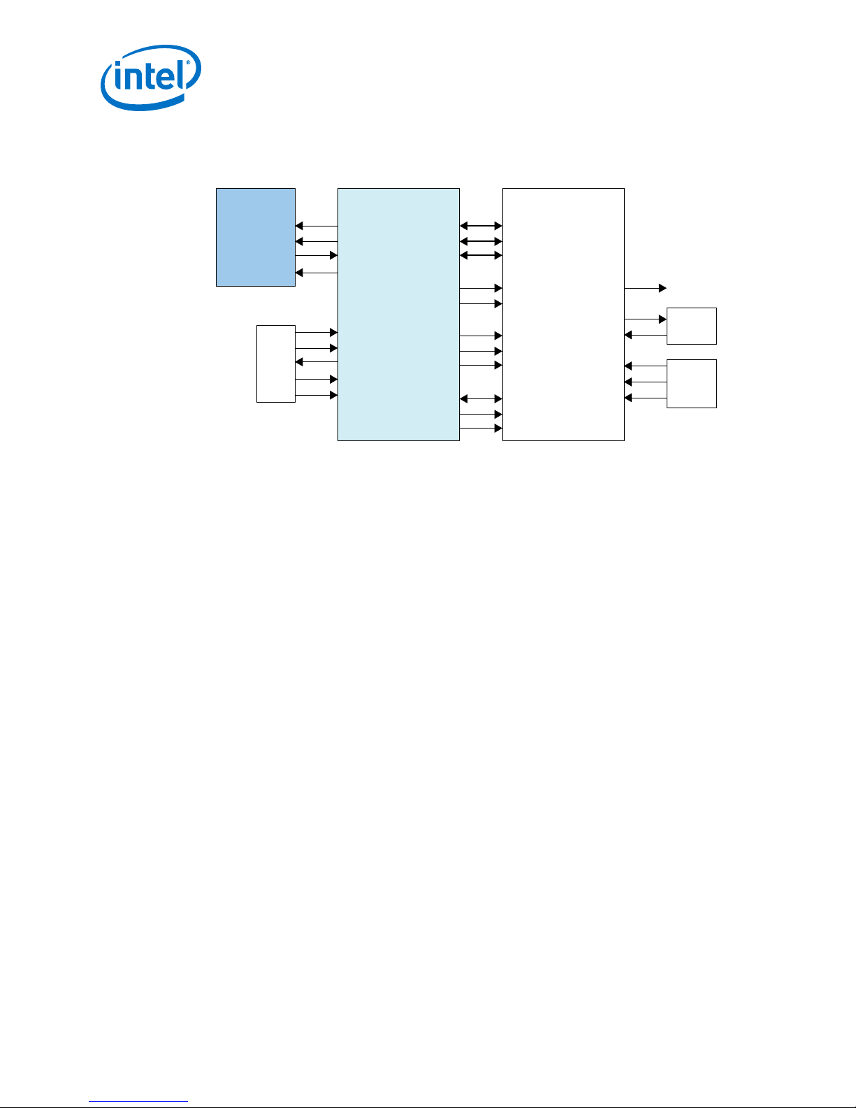
The figure below shows the conceptual block diagram for the embedded USB-Blaster.
USB2 PHY
USB MAX 10
FMCA & FMCB
Stratix 10 GX
MAX V
*TCK
*TDI
*TDO
*TMS
TCK
TDI
TDO
TMS
EXT_JTAG_TCK
EXT_JTAG_TDI
EXT_JTAG_TDO
EXT_JTAG_TMS
BLASTER_DISn
JTAG
Header
IO[7:0]
IO[15:8]
IO[23:16]
RDn
WRn
FLAG-A
FLAG-B
FLAG-C
SDA
SCL
RESETn
PORTA_IO[7:0]
PORTB_IO[7:0]
PORTD_IO[7:0]
RDY0
RDY1
CTL0
CTL1
CTL2
SDA
SCL
RESETn
IFCLK
XTAL-IN
XTAL-OUT
WAKEUP
USB_D+
USB_B-
Oscillator
24 MHz
5V
P
N
USB Connector
Type B
CY7C68013A_QFN10M04SCU169
USB_CLK
Figure 5. USB-Blaster II Block Diagram
The embedded USB-Blaster core for USB-based configuration of the Intel Stratix 10
GX FPGA device is implemented using a Type-B USB connector, a CY7C68013A USB2
PHY device, and an Intel Intel MAX 10 10M04SCU169 FPGA. This will allow
configuration of the Intel Stratix 10 GX FPGA device using a USB cable directly
connected to a computer running Intel Quartus Prime software without requiring the
external USB-Blaster dongle. This design will convert USB data to interface with the
Intel Stratix 10 GX FPGA's dedicated JTAG port. Four LEDs are provided to indicate
USB Blaster activity. The embedded USB Blaster is automatically disabled when an
external USB Blaster dongle is connected to the JTAG header.
4 Board Components
4.4.2 FPGA Programming from Flash Memory
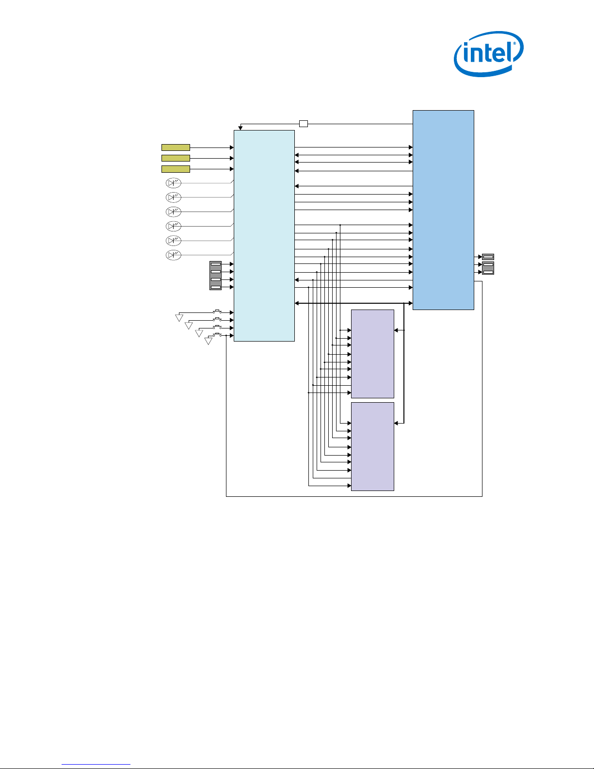
The figure below shows a detailed schematic block diagram for the MAX V + Flash
AvSTx32 mode configuration implementation.
Note: Typical JTAG clock frequency for CFI Flash programming via PFL II core is 16 MHz. You
may try it with a lower frequency such as 6 MHz if it fails with 16 MHz.
Intel® Stratix® 10 GX Transceiver Signal Integrity Development Kit User Guide
24
Page 25
MAX V System Controller
Intel Stratix 10 GX
MSEL0
MSEL1
MSEL2
CPU_RESET
ERROR
nCONFIG
nSTATUS
CONF_DONE
INIT_DONE
AvST_READY
AvST_CLK
FPGA_DATA[31:0]
AvST_VALID
FA[26:1]
FCLK
FCEn
FOEn
FWEn
FWPn
FADVn
WAIT
FRSTn
FLASH_D[31:0]
nCONFIG
nSTATUS
CONF_DONE
INIT_DONE
AvST_READY
AvST_CLK
D[31:0]
AvST_VALID
FA[26:1]
FCLK
FCEn
FOEn
FWEn
FWPn
FADVn
WAIT
RESETn
FLASH_D[31:0]
OSC_CLK_1
U6
FPGA_OSC_CLK_1MAX_OSC_CLK_1
FA[26:1]
CLK
CEn
OEn
WEn
WPn
ADVn
WAIT
RESETn
FD[15:0]
PC28F00AP30BF
Flash (1G)
FA[26:1]
CLK
CEn
OEn
WEn
WPn
ADVn
WAIT
RESETn
FD[15:0]
PC28F00AP30BF
Flash (1G)
SW11
SW10
X4 100 MHz
CLK_CONFIG
U1 50 MHz
CLK_50M_MAX5
U9 48 MHz
USB_MAX5_CLK
Error
D23
LOAD
D24
CONF_DONE
D25
PGM0
D20
PGM1
D21
PGM2
D22
LOAD
CONF_DONE
PGM_LED0
PGM_LED1
PGM_LED2
SW6
Factory Load
MAX V Switch
MAX V Switch
MAX V Switch
MAX_RESETn
PGM_CONFIG
PGM_SEL
CPU_RESETn
S12
S11
S10
S13
5M2210ZF256
125 MHz
4 Board Components
Figure 6. MAX V + Flash AvSTx32 Configuration Block Diagram
Once the FPGA is successfully initialized and in user mode, the CPLD will tri-state its
Flash interface signals to avoid contention with the FPGA. The PGMSEL dipswitch (S10)
is provided to select between two POF files (FACTORY and USER) stored on the Flash.
The Parallel Flash Loader II (PFL II) Megafunction is used to implement the AvSTx32
configuration in the MAX V CPLD. The PFL II Megafunction reads data from the flash
and converts it to AvST format. This data is written into the Intel Stratix 10 GX FPGA
device through dedicated AvST CLK and FPGA Config Data [31:0] pins at
corresponding clock rate, such as 25 MHz, 50 MHz and 100 MHz.
Implementation will be done using an Intel MAX V 5M2210ZF256FBGA CPLD acting as
the AvST download controller and two 1G Flash devices. The Flash will be Numonyx
1.8V core, 1.8V I/O 1Gigabit CFI NOR-type device (P/N: PC28F00AP30BF). The MAX V
CPLD shares the CFI Flash interface with the Intel Stratix 10 GX FPGA. No arbitration
is needed between MAX V CPLD and Intel Stratix 10 GX FPGA to access the Flash as
the CPLD only has access prior to FPGA initialization.
Intel® Stratix® 10 GX Transceiver Signal Integrity Development Kit User Guide
25
Page 26
4 Board Components
After a POWER-ON or RESET (reconfiguration) event, the MAX V device shall configure
the Intel Stratix 10 GX FPGA in the AvSTx32 mode with either the FACTORY POF or
an USER DEFINED POF depnding on the FACTORY_LOAD setting.
The MSEL[2:0] pins indicate which configuration scheme is chosen. The
manufacturing default condition is [000] for AvSTx32 scheme.
For different configuration modes, MSEL [2:0] signals must be set acccording to the
table below:
Table 6. Support Configuration Modes for Stratix 10 Transceiver Signal Integrity
Development Kit
Configuration Scheme
Avalon-ST (x32)
Avalon-ST (x16)
AS (Normal mode)
JTAG only
Not supported
000
101
011
111
Other Settings
4.4.3 FPGA Programming over External USB-Blaster
The JTAG chain allows programming of both the Intel Stratix 10 GX FPGA and MAX V
CPLD devices using an external USB-Blaster dongle or the on-board USB-II Blaster via
the USB Interface Connector.
During board bring-up, and as a back-up in case the on-board USB-Blaster II has a
problem, the external USB-Blaster dongle can be used to program both the Intel
Stratix 10 and MAX V CPLD via the external blaster 2x5 pin 0.1" programming header
(J14)
Another 2x5 pin 0.1" vertical non-shrouded header (J15) is provided on the board for
programming the Intel MAX 10_Blaster FPGA for configuring the on-board USB Blaster
circuitry. Once the on-board Blaster is configured and operational, the on-board
blaster can be used for subsequent programming of the Intel Stratix 10 GX FPGA and
MAX V CPLD.
The on-board blaster JTAG chain connects four JTAG nodes in the following order, with
the option to bypass the Intel Stratix 10, MAX V, FMC A or FMC B by a dip switch SW3
setting as follows:
• Switch closed/ON: Corresponding JTAG node is bypassed.
• Switch open/OFF: Corresponding JTAG node is enabled in the JTAG chain.
MSEL [2:0]
Pin 2 of the J14 Header is used to disable the embedded USB Blaster by connecting it
to the embedded Blaster's low active disable pin with a pull-up resistor. Since Pin 2
from the mating Blaster dongle is GND, when the dongle is connected into the JTAG
header, the embedded Blaster is disabled to avoid contention with the external USB
Blaster dongle.
Intel® Stratix® 10 GX Transceiver Signal Integrity Development Kit User Guide
26
Page 27
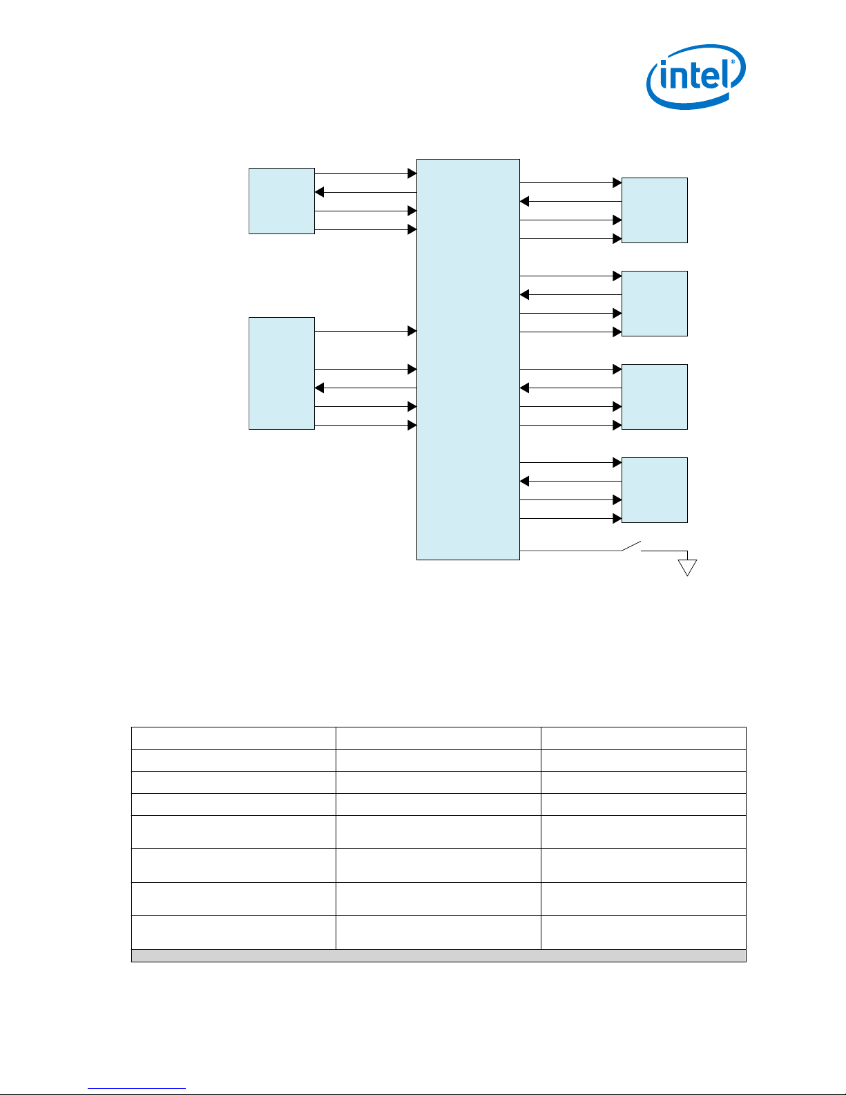
Intel
Stratix 10
U43
MAX V
U20
USB-PHY
U9
USB_MAX_TCK
USB_MAX_TDO
USB_MAX_TMS
USB_MAX_TDI
S10_JTAG_TCK
S10_JTAG_TDO
S10_JTAG_TMS
S10_JTAG_TDI
M5_JTAG_TCK
M5_JTAG_TDO
M5_JTAG_TMS
M5_JTAG_TDI
FMC-A
J58
FATCK
FATDO
FATMS
FATDI
FMC-B
J59
FBTCK
FBTDO
FBTMS
FBTDI
External
JTAG
Header
J14
EXT_JTAG_TCK
EXT_JTAG_TDO
EXT_JTAG_TMS
EXT_JTAG_TDI
BLASTER_DISn
USB MAX 10 FPGA
U97
xxJTAG_BYPASSn
4 Board Components
Figure 7. JTAG Chain
4.5 Status Elements
The development board includes board-specific status LEDs and switches for enabling
and configuring various features on the board, as well as 16 character x 2 line LCD for
Table 7. Board Specific LEDs
D29 --- Green LED. Power 3.3V present.
D31 --- Green LED. Power 3.3V PRE present.
D32 --- Green LED. Power 12V present.
D5
D6
D36
D1
displaying board power and temperature measurements. This section describes these
status elements.
Board Reference Signal Name Description
FAPRSNT_N
FBPRSNT_N
ERR_LED_N
JTAG_RX
Green LED. FMC A daughter card
present.
Green LED. FMC B daughter card
present.
Amber LED. System Power error
indicator.
Green LED. JTAG receiver activity
indicator.
continued...
Intel® Stratix® 10 GX Transceiver Signal Integrity Development Kit User Guide
27
Page 28
D2
D3
D4
D7
D8
D9
D10
D11
D27
4 Board Components
Board Reference Signal Name Description
JTAG_TX
SC_RX
SC_TX
ENET_LED_TX
ENET_LED_RX
ENET_LED_LINK1000
ENET_LED_LINK100
ENET_LED_LINK10
OVERTEMPn
Green LED. JTAG transmitter activity
indicator.
Green LED. System console receiver
activity indicator.
Green LED. System console
transmittter activity indicator.
Green LED. Blinks to indicate Ethernet
PHY transmit activity.
Green LED. Blinks to indicate Ethernet
PHY activity.
Green LED. Illuminates to indicate
Ethernet linked at 1000 Mbps
connection speed.
Green LED. Illuminates to indicate
Ethernet linked at 100 Mbps connection
speed.
Green LED. Illuminates to indicate
Ethernet linked at 10 Mbps connection
speed.
Amber LED. Intel Stratix 10 over
temperature indicator.
4.6 Setup Elements
This development board includes several different kinds of setup elements. This
section describes the following setup elements:
• JTAG Chain Device removal switch
• Program Select pushbutton
• MAX V Reset pushbutton
• CPU Reset pushbutton
JTAG Chain Device Removal Switch
The JTAG chain connects the Intel Stratix 10 GX FPGA, the MAX V CPLD, FMC A and
FMC B in a chain, with the option to selectively bypass each JTAG node by four dip
switch setting.
Program Select Pushbutton
After a POWER-ON or RESET (reconfiguration) event, the MAX V configures the Intel
Stratix 10 GX FPGA in the AvST mode with either the FACTORY POF or a USER-
DEFINED POF depending on FACTORY_LOAD setting. The setting of the PGMSEL bit is
selected by the PGMSEL pushbutton. Pressing this pushbutton and observing the
program LEDs (FACTORY or USER) dictates the program selection. Then, the
PGM_CONFIG pushbutton must be pressed to load the program.
Intel® Stratix® 10 GX Transceiver Signal Integrity Development Kit User Guide
28
Page 29

4 Board Components
MAX V Reset Pushbutton
This pushbutton is the development board's Master Reset. This pushbuttton is
connected to the MAX V CPLD (MAX_RESETn pin) that is used for AvST configuration.
When this button is pressed, the MAX V CPLD initiates a reloading of the stored image
from flash memory using AvST configuration mode. The image that is reloaded
depends on the PGMSEL setting.
CPU Reset Pushbutton
This pushbutton is the Nios II CPU Reset. This button is connected to a Intel Stratix 10
GX FPGA global signal input pin and can be used by Nios II implementations as a
dedicated CPU Reset button. This button is also connected to the MAX V CPLD so that
the FPGA device can be reset right after its configuration with AvST mode.
4.7 User Input-Output Components
This section describes the user I/O interface to the FPGA. The following I/O elements
are described:
• User-defined pushbuttons
• User-defined DIP switches
• User-defined LEDs
• Character LCD
4.7.1 User-Defined Pushbuttons
The development kit includes 8 user-defined pushbuttons and 4 system pushbuttons
that allow you to interact with the Intel Stratix 10 GX FPGA. When you press and hold
down the pushbutton, the device pin is set to logic 0; when you release the
pushbutton, the device pin is set to logic 1. There is no board-specific function for
these general user pushbuttons.
The table below lists the pushbuttons, schematic signal names and their corresponding
Intel Stratix 10 GX FPGA device pin numbers.
Table 8. User-Defined Pushbuttons
Board Reference Schematic Signal Name Description Intel Stratix 10 Device
S2
S3
S4
S5
S6
S7
S8
S9
S10
USER_PB0
USER_PB1
USER_PB2
USER_PB3
USER_PB4
USER_PB5
USER_PB6
USER_PB7
PGM_SEL
Pin Number
User pushbutton BG17
User pushbutton BE17
User pushbutton BH18
User pushbutton BJ19
User pushbutton BF17
User pushbutton BH17
User pushbutton BJ18
User pushbutton BJ20
System pushbutton N/A
continued...
Intel® Stratix® 10 GX Transceiver Signal Integrity Development Kit User Guide
29
Page 30

4 Board Components
Board Reference Schematic Signal Name Description Intel Stratix 10 Device
S11
S12
S13
PGM_CONFIG
MAX_RESETn
CPU_RESETn
4.7.2 User-Defined DIP Switch
Board reference SW4 and SW5 are two 4-pin DIP switches. The switches are userdefined and are provides additional FPGA input control. When the switch is in the
OPEN position, a logic 1 is selected. When the switch is in the CLOSED or ON position,
a logic 0 is selected. There is no board-specific function for these switches.
The table below lists the schematic signal names of each DIP switch and their
corresponding Intel Stratix 10 GX FPGA pin numbers.
Table 9. User-Defined Switches
Board Reference Schematic Signal Name Intel Stratix 10 GX Device Pin
SW5.4
SW5.3
SW5.2
SW5.1
SW4.4
SW4.3
SW4.2
SW4.1
USER_DIP0
USER_DIP1
USER_DIP2
USER_DIP3
USER_DIP4
USER_DIP5
USER_DIP6
S10_UNLOCK
Pin Number
System pushbutton N/A
System pushbutton N/A
System pushbutton AW10
Number
AV20
AV21
AT19
BE19
BB18
BC18
BD18
BG18
4.7.3 User-Defined LEDs
The development board includes 8 user-defined LEDs. Board references D12 through
D19 are user LEDs that allow status and debugging signals to be driven to the LEDs
from the designs loaded into the Intel Stratix 10 GX FPGA device. The LEDs illuminate
when a logic 0 is driven and turns off when a logic 1 is driven. There is no boardspecific function for these LEDs.
The table below lists the user-defined schematic signal names and their corresponding
Intel Stratix 10 GX FPGA device pin numbers.
Table 10. User-Defined LEDs
Board Reference Schematic Signal Name Intel Stratix 10 Device Pin Number
D12
D13
D14
D15
Intel® Stratix® 10 GX Transceiver Signal Integrity Development Kit User Guide
30
USER_LED0
USER_LED1
USER_LED2
USER_LED3
BC21
BC20
BA20
BA21
continued...
Page 31

4 Board Components
Board Reference Schematic Signal Name Intel Stratix 10 Device Pin Number
D16
D17
D18
D19
USER_LED4
USER_LED5
USER_LED6
USER_LED7
4.7.4 Character LCD
A 16 character x 2 line LCD display is connected to the Intel Stratix 10 GX FPGA
device to display board information and IP address. The LCD module used is New
Haven - NHD-0216K3Z-NSW-BBW-V3. This LCD module will be mounted to the Intel
Stratix 10 GX transceiver signal integrity development board using a 1x10 vertical
male 0.1" header on the left side of the module and three plastic standoffs. This
mounting scheme allows low profile (less than 0.5 inches in height) components to be
placed underneath the LCD module, preserving board real-estate.
The table below summarizes the LCD pin assignments. This signal names and
directions are relative to the Intel Stratix 10 GX FPGA.
Table 11. LCD Pin Assignments and Schematic Signal Names
BD21
BB20
AW21
AY21
Board Reference Schematic Signal Name Description
7
8
I2C_5V_SCL
I2C_5V_SDA
4.8 Clock Circuits
4.8.1 Transceiver Dedicated Clocks
Dedicated clocking scheme that is implemented on the Intel Stratix 10 GX transceiver
signal integrity development board allows four different protocols to run
simultaneously by the Intel Stratix 10 GX FPGA.
Four differential clock sources are provided from an I2C programmable VCO oscillator
or PLL to the dedicated REFCLK input pins of transceiver blocks on both sides of the
FPGA. The default frequencies for these two oscillators and PLLs at startup are:
• 644.53125 MHz (Y1 left side xcvrs and U6 right side xcvrs)
• 706.25 MHz (Y2 right side xcvrs)
• 625 MHz (U5 left side xcvrs and U6 right side xcvrs)
• 614.4 MHz (U5 left side xcvrs)
The default frequencies can be overridden and a different frequency can be
programmed into the oscillators and PLLs for support of other protocols.
I2C serial clock
I2C serial data
Note:
Programmed frequencies are lost upon a board power down. Oscillator and PLL
frequencies return to their default frequency upon power up.
Each oscillator or PLL provides a differential LVDS trigger output to SMA connectors for
scope or other lab equipment triggering purposes.
Intel® Stratix® 10 GX Transceiver Signal Integrity Development Kit User Guide
31
Page 32

In addition to the two oscillators and PLLs, each sides have two dedicated differential
(FMCA)
(U4)
4N
FAGBTCLKM2Cp/n3
CLK_FMCA_706M_p/n
(FMCA)
(U6)
4M
FAGBTCLKM2Cp/n2
CLK_GXBR4M_625M_p/n
(FMCA)
(U6)
4L
FAGBTCLKM2Cp/n1
CLK_GXBR4L_644M_p/n
(FMCA)
(SMA)
4K
FAGBTCLKM2Cp/n0
CLKIN_SMA_4K_p/n
(U4)
(U6)
4F
CLK_MXP3_706M_p/n
CLK_GXBR4F_644M_p/n
(U4)
(U6)
4E
CLK_MXP2_706M_p/n
CLK_GXBR4E_644M_p/n
(U4)
(U6)
4D
CLK_MXP1_706M_p/n
CLK_GXBR4D_644M_p/n
(U4)
(SMA)
4C
CLK_SMA_706M_p/n
CLKIN_SMA_4C_p/n
(FMCB)
(U3)
1N
FBGBTCLKM2Cp/n1
CLK_FMCB_644M_p/n
(FMCB)
(SMA)
1M
FBGBTCLKM2Cp/n0
CLKIN_SMA_1M_p/n
(U5)
1L
CLK_GXBR1L_625M_p/n
(U3)
(U5)
1K
CLK_SFP_644M_p/n
CLK_GXBL1K_614M_p/n
(U5)
1F
CLK_GXBL1F_625M_p/n
(U5)
(U5)
1E
CLK_GXBL1E_614MT_p/n
CLK_GXBL1E_614MT_p/n
(U3)
(U3)
1D
CLK_QSFP0_644MT_p/n
CLK_QSFP0_644MB_p/n
(U3)
(SMA)
1C
CLK_CFP4_644M_p/n
CLKIN_SMA_1C_p/n
Stratix 10 GX
Clock
Buffer
U4
OSC
SEL
Trigger
PLL
U6
Crystal
Trigger
Clock
Buffer
U3
OSC
SEL
Trigger
PLL
U5
Crystal
Trigger
REFCLK input from a pair of SMA connectors to allow use of lab equipment clock
generators as the transceiver clock source.
The four inputs below connect directly to the transceiver clock inputs:
•
J65/J66 SMA connectors direct connection to REFCLK_GXB1C block
•
J67/J68 SMA connectors direct connection to REFCLK_GXB1M block
•
J69/J70 SMA connectors direct connection to REFCLK_GXB4C block
•
J71/J72 SMA connectors direct connection to REFCLK_GXB4K block
The figure below shows the dedicated transceiver clocks that are implemented on the
Intel Stratix 10 GX FPGA development kit.
Figure 8. Transceiver Dedicated Clocks
4 Board Components
4.8.2 General-Purpose Clocks
In addtion to transceiver dedicated clocks, five other clock sources are provided to the
FPGA Global CLK inputs for general FPGA design as shown in the figure below.
The usage of these clocks is as follows:
Intel® Stratix® 10 GX Transceiver Signal Integrity Development Kit User Guide
32
Page 33

(FMCA)
(FMCA)
3L
FACLKBIDIRp/n2
FACLKBIDIRp/n3
(FMCA)
(FMCA)
3K
FACLKM2Cp/n1
FALAp/n17
(U6)
3J
CLK_S10TOP_125M_p/n
(FMCA)
(FMCA)
3I
FAHAp/n0
FAHAp/n17
(U6)
SDM
FPGA_OSC_CLK_1
(SMA)
(SMA)
3C
CLKOUT_SMA_3C_p/n
CLKIN_SMA_3C_p/n
(U1)
3B
CLK_50M_S10
3A
(U2)
(FMCB)
2N
CLK_S10TOP_ADJ_p/n
FBCLKM2Cp/n1
(FMCB)
(FMCB)
1M
FBCLKM2Cp/n0
FABLp/n0
(FMCA)
2L
FACLKM2Cp/n0
(U9)
2F
USB_FPGA_CLK
2C
2B
(U5)
2A
CLK_S10BOT_100M_p/n
Stratix 10 GX
(FMCA)
FALAp/n0
4 Board Components
• 50 MHz oscillator through an SL18860 buffer for Nios II applications.
USB_FPGA_CLK drives from on-board Intel FPGA Download Cable circuit.
• 25 MHz crystal supplied to an ICS557-03 Spread Spectrum differential clock
buffer. The available frequencies and down spread percentages available from the
spread spectrum buffer as shown in the table below.
• External differential clock source from SMA connectors. Dedicated differential
output clock to SMA connectors.
• Three clock outputs are provided from two Si5341 PLLs:
—
CLK_S10_BOT_100M: 100 MHz LVDS standard
—
CLK_S10_TOP_125M: 125 MHz LVDS standard
—
FPGA_OSC_CLK_1: 125 MHz 1.8V CMOS standard
• Another clock source is clock from FMC daughter cards.
Figure 9. FPGA Clocks
Table 12. Spread Spectrum Clock Settings and Frequencies
0 0 25 (Default) Center+/-0.25
Spread Spectrum Buffer (Inputs) Output Clock Select
SS1/S1 SS0/S0
(MHz)
Intel® Stratix® 10 GX Transceiver Signal Integrity Development Kit User Guide
Spread (%)
continued...
33
Page 34

4 Board Components
Spread Spectrum Buffer (Inputs) Output Clock Select
0 1 100 Down -0.5
1 0 125 Down -0.75
1 1 200 No Spread
(MHz)
4.8.3 Embedded USB-Blaster Clock
A 24 MHz crystal is dedicated for the embedded USB-Blaster II circuit. The crystal is
used to clock the Cypress CY7C68013A USB2 PHY device.
4.9 Transceiver Channels
The Intel Stratix 10 GX transceiver signal integrity development kit dedicates 78
channels from both the left and right sides of the device. Transceiver channels are
allocated as shown in the table below.
Table 13. Stratix 10 GX FPGA Transceiver Channels
Transceiver Channel Data Rate Number of Channels
2.4 mm RF Platinum channel 17.4 Gbps or 28.3 Gbps (applies to
GXT channels only)
2.4 mm RF Gold channel 17.4 Gbps or 28.3 Gbps (applies to
GXT channels only)
2.4 mm RF channels 17.4 Gbps or 28.3 Gbps (applies to
GXT channels only)
MXP connector 0 17.4 Gbps or 28.3 Gbps (applies to
GXT channels only)
MXP connector 1 17.4 Gbps or 28.3 Gbps (applies to
GXT channels only)
MXP connector 2 17.4 Gbps or 28.3 Gbps (applies to
GXT channels only)
CFP4 Optical Interface 17.4 Gbps or 28.3 Gbps (applies to
GXT channels only)
QSFP28 0 Optical Interface 17.4 Gbps or 28.3 Gbps (applies to
GXT channels only)
QSFP28 1 Optical Interface 17.4 Gbps or 28.3 Gbps (applies to
GXT channels only)
SFP+ 0 Optical Interface 14 Gbps 1
SFP+ 1 Optical Interface 14 Gbps 1
FMC A Interface 17.4 Gbps or 28.3 Gbps (applies to
GXT channels only)
FMC B Interface 17.4 Gbps or 28.3 Gbps (applies to
GXT channels only)
External loopback Interface 17.4 Gbps or 28.3 Gbps (applies to
GXT channels only)
1
1
4
4
4
4
4
4
4
24
16
6
Spread (%)
Intel® Stratix® 10 GX Transceiver Signal Integrity Development Kit User Guide
34
Page 35

4N
Stratix 10 GX
GX
GXT
GXT
GX
GXT
GXT
4M
GX
GXT
GXT
GX
GXT
GXT
4L
GX
GXT
GXT
GX
GXT
GXT
4K
GX
GXT
GXT
GX
GXT
GXT
4F
GX
GXT
GXT
GX
GXT
GXT
4E
GX
GXT
GXT
GX
GXT
GXT
4D
GX
GXT
GXT
GX
GXT
GXT
4C
GX
GXT
GXT
GX
GXT
GXT
1N
GX
GXT
GXT
GX
GXT
GXT
1M
GX
GXT
GXT
GX
GXT
GXT
1L
GX
GXT
GXT
GX
GXT
GXT
1K
GX
GXT
GXT
GX
GXT
GXT
1F
GX
GXT
GXT
GX
GXT
GXT
1E
GX
GXT
GXT
GX
GXT
GXT
1D
GX
GXT
GXT
GX
GXT
GXT
1C
GX
GXT
GXT
GX
GXT
GXT
FMC+ A
TX/RX (X24)
FMC+ B
TX/RX (X16)
MXP 2
TX/RX (X4)
MXP 1
TX/RX (X4)
MXP 0
TX/RX (X4)
2.4 mm
SMA
TX/RX (X6)
QSFP28 0
TX/RX (X4)
CFP4
TX/RX (X4)
QSFP28 1
TX/RX (X4)
External
Loopback
TX/RX (X6)
SFP+ 1
TX/RX (X1)
SFP+ 0
TX/RX (X1)
Platinum
Gold
4 Board Components
Figure 10. Stratix 10 GX FPGA Transceiver Usage Block Diagram
Table 14. 2.4 mm RF Interface
GXB_4C_TXp/n[5:0]
GXBR_4C_RXp/n[5:0]
Schematic Signal Name Stratix 10 FPGA Pin Number Description
Positive pin location increases from
2.4 mm RF GXB Transmitter
index 0: BJ4, BF5, BG3, BE3, BF1, BC3
Positive pin location increases from
2.4 mm RF GXB Receiver
index 0: BH9, BJ7, BG7, BE7, BC7,
BD5
Intel® Stratix® 10 GX Transceiver Signal Integrity Development Kit User Guide
35
Page 36

Table 15. MXP Interface
8 7 6 5 4 3 2 1
9 10 11 12 13 14 15 16
RXN0 RXP0 RXN1 RXP1 RXN3 RXP3 RXN4 RXP4
TXN0 TXP0 TXN1 TXP1 TXN3 TXP3 TXN4 TXP4
Schematic Signal Name Stratix 10 FPGA Pin Number Description
GXBL_4D_TXp/n[1:0][4:3]
GXBL_4D_RXp/n[1:0][4:3]
GXBL_4E_TXp/n[1:0][4:3]
GXBL_4E_RXp/n[1:0][4:3]
GXBL_4F_TXp/n[1:0][4:3]
GXBL_4F_RXp/n[1:0][4:3]
Positive pin location increases from
index 0: BD1, BA3, AW3, AY1
Positive pin location increases from
index 0: BA7, BB5, AY5, AU7
Positive pin location increases from
index 0: AV1, AR3, AP1, AN3
Positive pin location increases from
index 0: AR7, AT5, AN7, AM5
Positive pin location increases from
index 0: AK1, AL3, AJ3, AF1
Positive pin location increases from
index 0: AL7, AH5, AF5, AG7
Figure 11. MXP connector pin function mapping
4 Board Components
MXP 1 GXB Transmitter
MXP 1 GXB Receiver
MXP 2 GXB Transmitter
MXP 2 GXB Receiver
MXP 3 GXB Transmitter
MXP 3 GXB Receiver
Table 16. Optical Modules Interface
Schematic Signal Name Intel Stratix 10 FPGA Pin Number Description
GXBL_1C_TXp/n[1:0][4:3]
GXBL_1C_RXp/n[1:0][4:3]
GXBL_1D_TXp/n[1:0][4:3]
GXBL_1D_RXp/n[1:0][4:3]
GXBL_1E_TXp/n[1:0][4:3]
GXBL_1E_RXp/n[1:0][4:3]
GXBL_1K_TXp/n 0/3
GXBL_1K_RXp/n 0/3
Positive pin location increases from
index 0: BJ46, BF45, BE47, BF49
Positive pin location increases from
index 0: BH41, BJ43, BE43, BC43
Positive pin location increases from
index 0: BD49, BA47, AW47, AY49
Positive pin location increases from
index 0: BA43, BB45, AY45, AU43
Positive pin location increases from
index 0: AV49, AR47, AP49, AN47
Positive pin location increases from
index 0: AR43, AT45, AN43, AM45
Positive pin location increases from
index 0: AE47, AA47
Positive pin location increases from
index 0: AC43, AB45
CFP4 GXB Transmitter
CFP4 GXB Receiver
QSFP28 0 GXB Transmitter
QSFP28 0 GXB Receiver
QSFP28 1 GXB Transmitter
QSFP28 1 GXB Receiver
SFP+ 0/1 GXB Transmitter
SFP+ 0/1 GXB Receiver
Intel® Stratix® 10 GX Transceiver Signal Integrity Development Kit User Guide
36
Page 37

4 Board Components
Table 17. FMC Interface
Schematic Signal Name Intel Stratix 10 FPGA Pin Number Description
FAC2Mp/n[23:0]
FAM2Cp/n[23:0]
FBC2Mp/n[15:0]
FBM2Cp/n[15:0]
Positive pin location increases from
index 0: AE3, AC3, AD1, AA3, AB1,
W3, Y1, V1, U3, T1, P1, R3, M1, N3,
K1, L3, H1, J3, F1, G3, D1, E3, C3, B5
Positive pin location increases from
index 0: AC7, AD5, AA7, AB5, W7, Y5,
V5, U7, T5, P5, R7, M5, N7, K5, L7,
H5, J7, F5, G7, D5, E7, C7, A7, B9
Positive pin location increases from
index 0: U47, T49, P49, R47, M49,
N47, K49, L47, H49, J47, F49, G47,
D49, E47, C47, B45
Positive pin location increases from
index 0: T45, P45, R43, M45, N43,
K45, L43, H45, J43, F45, G43, D45,
E43, C43, A43, B41
Table 18. External Loopback Interface
Schematic Signal Name Intel Stratix 10 FPGA Pin Number Description
GXBL_1F_TXp/n[5:0]
GXBL_1F_RXp/n[5:0]
Positive pin location increases from
index 0: AK49, AL47, AH49, AJ47,
AF49, AG47
Positive pin location increases from
index 0: AL43, AH45, AJ43, AF45,
AG43, AE43
FMC A GXB Transmitter
FMC A GXB Receiver
FMC B GXB Transmitter
FMC B GXB Receiver
External loopback GXB Transmitter
External loopback GXB Receiver
4.10 Communication Ports
The Intel Stratix 10 GX transceiver signal integrity development board supports a
10/100/1000 BASE-T Ethernet connection using a Marvell 88E1111 PHY device and the
Intel Triple-Speed Ethernet Megacore MAC function. The device is an auto-negotiating
Ethernet PHY with an SGMII interface to the FPGA.
The Intel Stratix 10 GX FPGA device can communicate with the LVDS interfaces at up
to 1.25 Gbps. The MAC function is provided in the FPGA for typical networking
applications. The Marvell 88E1111 PHY uses 2.5 V and 1.2 V power rails and requires
a 25-MHz reference clock driven from a dedicated oscillator. It interfaces to an RJ-45
connector with internal magnetics that are used for driving copper lines with Ethernet
traffic.
Table 19. Ethernet PHY Pin Assignments
Schematic Signal Name Marvell 88E1111 (U23) PHY Pin
ENET_LED_LINK1000
ENET_LED_LINK100
ENET_LED_LINK10
ENET_LED_TX
ENET_LED_RX
60/73 1000 Mb link LED
74 100 Mb link LED
59/76 10 Mb link LED
68 TX data active LED
69 RX data active LED
Number
Description
continued...
Intel® Stratix® 10 GX Transceiver Signal Integrity Development Kit User Guide
37
Page 38

4 Board Components
Schematic Signal Name Marvell 88E1111 (U23) PHY Pin
ENET_SGMII_TX_P
ENET_SGMII_TX_N
ENET_SGMII_RX_P
ENET_SGMII_RX_N
ENET_XTAL_25MHZ
ENET_T_INTn
ENET_RSET
MDIO_T
MDC_T
MDI_P0
MDI_N0
MDI_P1
MDI_N1
MDI_P2
MDI_N2
MDI_P3
MDI_N3
82 SGMII transmit
81 SGMII transmit
77 SGMII receive
75 SGMII receive
55 25 MHz clock
23 Management bus interrrupt
30 Device reset
24 Management bus data input/output
25 Management bus data clock
29 Management bus data
31 Management bus data
33 Management bus data
34 Management bus data
39 Management bus data
41 Management bus data
42 Management bus data
43 Management bus data
Number
Description
4.11 Flash Memory
The development board has two 1-Gbit CFI compatible synchronous flash device for
non-voltaile storage of the FPGA configuration data, board information, test application
data and user code space.
Two flash devices are implemented to achieve a 32-bit wide data bus at 16 bits each
per device. The target device is a Micron PC28F00AP30BF CFI Flash device. Both MAX
V CPLD and Intel Stratix 10 GX FPGA can access this Flash device.
MAX V CPLD accesses are for AvST configuration of the FPGA at power-on and board
reset events. It uses the PFL Megafunction. Intel Stratix 10 GX FPGA access to the
flash memory's user space is done by Nios II for the BUP application. The flash is
wired for WORD mode operation to support AvSTx32 download directly.
The table below shows the memory map for the on-board flash. This memory provides
non-volatile storage for two FPGA bit-streams as well as various settings for data used
for the Board Update Portal (BUP) image and on-board devices such as PFL II
configuration bits.
Intel® Stratix® 10 GX Transceiver Signal Integrity Development Kit User Guide
38
Page 39

4 Board Components
Table 20. Flash Memory Map
Block Description Size Address
Board Test System 512 KB
User Software 14,336 KB
Factory Software 8,192 KB
zipfs 8,192 KB
User Hardware 2 44,032 KB
User Hardware 1 44,032 KB
Factory Hardware 44,032 KB
PFL Option Bits 64 KB
Board Information 64 KB
Ethernet Option Bits 64 KB
User Design Reset 64 KB
Each FPGA bit-stream can be a maximum of 254.25 Mbits (or less than 32 MB) for the
Intel Stratix 10 GX FPGA device. The remaining area is designated as RESERVED flash
area for storage of the BUP image and PFL configuration settings, software binaries
and other data relevant to the FPGA design.
0x09F4.0000 - 09FB.FFFF
0x0914.0000 - 09F3.FFFF
0x0894.0000 - 0913.FFFF
0x0814.0000 -0893.FFFF
0x0564.0000 - 0813.FFFF
0x02B4.0000 - 0563.FFFF
0x0004.0000 - 02B3.FFFF
0x0003.0000 - 0003.FFFF
0x0002.0000 - 0002.FFFF
0x0001.0000 - 0001.FFFF
0x0000.0000 - 0000.FFFF
Table 21. Flash Memory Pin Assignments Table
Flash Memory Device Pin
Number (U33/U34)
A1 (U33/U34)
B1 (U33/U34)
C1 (U33/U34)
D1 (U33/U34)
D2 (U33/U34)
A2 (U33/U34)
C2 (U33/U34)
A3 (U33/U34)
B3 (U33/U34)
C3 (U33/U34)
D3 (U33/U34)
C4 (U33/U34)
A5 (U33/U34)
B5 (U33/U34)
C5 (U33/U34)
D7 (U33/U34)
Schematic Signal Name Description Intel Stratix 10 Device
FM_A1
FM_A2
FM_A3
FM_A4
FM_A5
FM_A6
FM_A7
FM_A8
FM_A9
FM_A10
FM_A11
FM_A12
FM_A13
FM_A14
FM_A15
FM_A16
Address Bus BB30
Address Bus BF31
Address Bus BG32
Address Bus BC35
Address Bus BG29
Address Bus BG30
Address Bus BH28
Address Bus BH31
Address Bus BF29
Address Bus BH32
Address Bus BD29
Address Bus BC36
Address Bus BA31
Address Bus BJ29
Address Bus BJ30
Address Bus BA32
Pin Number
continued...
Intel® Stratix® 10 GX Transceiver Signal Integrity Development Kit User Guide
39
Page 40

4 Board Components
Flash Memory Device Pin
Number (U33/U34)
D8 (U33/U34)
A7 (U33/U34)
B7 (U33/U34)
C7 (U33/U34)
C8 (U33/U34)
A8 (U33/U34)
G1 (U33/U34)
H8 (U33/U34)
B6 (U33/U34)
B8 (U33/U34)
F2 (U33)
E2 (U33)
G3 (U33)
E4 (U33)
E5 (U33)
G5 (U33)
G6 (U33)
H7 (U33)
E1 (U33)
E3 (U33)
F3 (U33)
F4 (U33)
F5 (U33)
H5 (U33)
G7 (U33)
E7 (U33)
F2 (U34)
E2 (U34)
G3 (U34)
E4 (U34)
E5 (U34)
G5 (U34)
G6 (U34)
H7 (U34)
Schematic Signal Name Description Intel Stratix 10 Device
FM_A17
FM_A18
FM_A19
FM_A20
FM_A21
FM_A22
FM_A23
FM_A24
FM_A25
FM_A26
FM_D0
FM_D1
FM_D2
FM_D3
FM_D4
FM_D5
FM_D6
FM_D7
FM_D8
FM_D9
FM_D10
FM_D11
FM_D12
FM_D13
FM_D14
FM_D15
FM_D16
FM_D17
FM_D18
FM_D19
FM_D20
FM_D21
FM_D22
FM_D23
Address Bus BE28
Address Bus AU30
Address Bus AT30
Address Bus BJ28
Address Bus BG28
Address Bus BE29
Address Bus BD36
Address Bus BH30
Address Bus BC31
Address Bus BC31
Data Bus AV33
Data Bus BC33
Data Bus BD33
Data Bus BJ33
Data Bus BF35
Data Bus AT32
Data Bus BB34
Data Bus BD34
Data Bus AU33
Data Bus AY34
Data Bus BB35
Data Bus BD35
Data Bus BA34
Data Bus BB33
Data Bus AV32
Data Bus BF34
Data Bus AW35
Data Bus BF36
Data Bus AW34
Data Bus BG34
Data Bus BG35
Data Bus BA36
Data Bus AT34
Data Bus AR32
Pin Number
continued...
Intel® Stratix® 10 GX Transceiver Signal Integrity Development Kit User Guide
40
Page 41

4 Board Components
Flash Memory Device Pin
Number (U33/U34)
E1 (U34)
E3 (U34)
F3 (U34)
F4 (U34)
F5 (U34)
H5 (U34)
G7 (U34)
E7 (U34)
E6 (U33/U44)
D4 (U33/U34)
B4 (U33)
B4 (U34)
F8 (U33/U34)
G8 (U33/U34)
F6 (U33/U34)
C6 (U33/U34)
F7 (U33)
F7 (U34)
Schematic Signal Name Description Intel Stratix 10 Device
FM_D24
FM_D25
FM_D26
FM_D27
FM_D28
FM_D29
FM_D30
FM_D31
FLASH_CLK
FLASH_RESETn
FLASH_CEn0
FLASH_CEn1
FLASH_OEn
FLASH_WEn
FLASH_ADVn
FLASH_WPn
FLASH_RDYBSYn0
FLASH_RDYBSYn1
Data Bus AU32
Data Bus BJ34
Data Bus BH35
Data Bus AV35
Data Bus AY36
Data Bus AU35
Data Bus AR31
Data Bus AT35
Clock BB29
Reset BF32
Chip Enable 0 BE32
Chip Enable 1 BF30
Output Enable BC30
Write Enable BE36
Address Valid BD30
Write Protect N/A
Ready/Busy BJ31
Ready/Busy AT29
Pin Number
Intel® Stratix® 10 GX Transceiver Signal Integrity Development Kit User Guide
41
Page 42

5 System Power
5 System Power
5.1 Power Guidelines
Intel Stratix 10 GX transceiver signal integrity development kits can be powered by
either Intel provided 240 W brick or a standard ATX power supply which provides
more than 240 W power.
Use Intel provided 24-pin to 6-pin adapter cable to hook up ATX power supply's 24-pin
ATX output with Intel Stratix 10 transceiver signal integrity development kit's J103
connector. Do not plug an ATX power supply 6-pin connector into J103 connector
directly.
You can supply power for VCC, VCCERAM, VCCRL, VCCRR, VCCT and VCCH rails with
external equipment by following the two steps outlined below for such kind of
application:
1. Turn OFF corresponding on-board regulators via SW9 or S14 dipswitch before
board power up.
2. Supply power with banana jacks (J92, J94) or power terminations (J19, J86, J89,
J91, J83 ). Manage the power-up and power-down sequence for on-board
regulators and external equipments with necessary tools (LTpowerplay).
5.2 Power Supply
Power supply for this development kit is provided through an external laptop style DC
power brick connected to a 6-pin ATX power connector. The input voltage is in the
range of 12V +/- 5%. This DC voltage is then stepped down to the various power rails
used by the components on the development board.
Important: The power rails on the development board have the option to be supplied from an
external source through a banana jack or power terminal connectors by first disabling
corresponding power regulator using SW9/S14 DIP Switch.
Table 22. Power per Device on the Development Board
Device Voltage Name Voltage Value (Volts) Note
S10_VCC
S10_VCCRL
Intel Stratix 10 GX FPGA
(1SG280UF2397)
Intel Corporation. All rights reserved. Intel, the Intel logo, Altera, Arria, Cyclone, Enpirion, MAX, Nios, Quartus
and Stratix words and logos are trademarks of Intel Corporation or its subsidiaries in the U.S. and/or other
countries. Intel warrants performance of its FPGA and semiconductor products to current specifications in
accordance with Intel's standard warranty, but reserves the right to make changes to any products and services
at any time without notice. Intel assumes no responsibility or liability arising out of the application or use of any
information, product, or service described herein except as expressly agreed to in writing by Intel. Intel
customers are advised to obtain the latest version of device specifications before relying on any published
information and before placing orders for products or services.
*Other names and brands may be claimed as the property of others.
S10_VCCRR
S10_VCCT
S10_VCCERAM
0.85/VID Core and periphery power
1.12/1.03 Left XCVR RX path
1.12/1.03 Right XCVR RX path
1.12/1.03 XCVR TX path
0.9 Memory and PLL digital
power
continued...
ISO
9001:2008
Registered
Page 43

5 System Power
Device Voltage Name Voltage Value (Volts) Note
USB Intel MAX 10
(10M04SCU169)
PWR Intel MAX 10
(10M16SAU169)
MAX V (EPM2210F256)
Flash (PC28F00AP30BFx2)
USB PHY (CY7C68103)
Ethernet PHY (88E1111)
Power Monitor (LTM2987)
Clock Buffer (SL18860DC)
SS Clock Generator
(ICS557)
Programmable Oscillator
(Si570x2)
Clock Buffer (Si533311x2)
Programmable PLL
(Si5341x2)
Power Measurement
(LTC2418)
DAC (DAC7578)
CFP4 Module
QSFP28 Modules
SFP+ Modules
S10_VCCH
1.8V
2.4V
FMCA_VADJ
FMCB_VADJ
3.3V_PRE
1.8V_PRE
3.3V_STBY
1.8V
1.8V
3.3V_PRE
2.5V
12V_IN
1.8V
3.3V
2.5V
1.8V
3.3V
5V
3.3V_STBY
3.3V
3.3V
3.3V
1.8 XCVR and PLL analog power
1.8 I/O voltage and I/O pre-
2.4
1.8/1.5/1.35/1.2 I/O Voltage
1.8/1.5/1.35/1.2 I/O Voltage
3.3
1.8
3.3 Intel Power Management
1.8 System Controller
1.8 CFI Flash
3.3 USB PHY
2.5 Ethernet PHY
12 Linear Tech Power
1.8 Core Clock Buffer
3.3 Spread Spectrum / Clock
2.5 Transceiver Reference Clock
1.8
3.3
5 Measure current in Intel
3.3 Trim voltage in Intel power
3.3 CFP4 Module
3.3 QSFP28 Modules
3.3 SFP+ Modules
drivers
VCCFUSEWR power
Core, PLL and VCCIO
VCCIO for Intel Stratix 10
Interface
Chip
Management Chip
Select capability to core
clock
Buffers
Transceiver Reference Clock
and Core Clock
power management solution
management solution
5.3 Power Management
Two power management solutions are provided in the Intel Stratix 10 GX Transceiver
Signal Integrity Development Kit:
• Linear Tech LTM2987
• Intel power Intel MAX 10 logic
You can select either of the aforementioned power management solutions by using
Sw8-3.
Intel® Stratix® 10 GX Transceiver Signal Integrity Development Kit User Guide
43
Page 44

LTM2987 or power Intel MAX 10 devices are capabale of measuring the voltage,
measuring the current, trimming the voltage and sequencing the order at power on
and power off. Voltages can be trimmed upto +/- 10%. Communication to these
devices is through I2C interface. A Linear Technology power monitor application known
as LTPowerPlay is utilized to measure, trim and observe each voltage rail's condition.
Table 23. Functions supported by the two Power Management Solutions
5 System Power
Rail Name LT/Intel Voltage
VCC
VCCRL
VCCRR
VCCT
VCCH
VCCERAM
1.8V
3.3V
2.5V
12V
Monitor
Y - - - Y
Y Y Y N* Y
Y Y Y N* Y
Y Y Y N* Y
Y Y Y N* Y
Y Y Y N* Y
Y Y Y N* Y
Y N N N Y
Y N N N Y
Y N - - Y
LT/Intel Current
Monitor
LT Voltage Trim Intel Voltage
Trim
LT/Intel PWR
Sequence
Control
Note: *: Default not supported, request for an example design if you want this feature.
5.4 Power Distribution System
The figure shows the power distribution system of the Intel Stratix 10 GX transceiver
signal integrity development kit.
Intel® Stratix® 10 GX Transceiver Signal Integrity Development Kit User Guide
44
Page 45

131 A, 83A
LTM4677
x3LTM4650
U63/U64/U66/U67
EN_VCC
S10_VCC
Stratix 10 VCC, VCCP
1 mΩ
18 A, 13 A
LTM4620
U68
EN_VCCERAM
S10_VCCERAM
Stratix 10 VCCERAM
131 W, 83 W
20 W, 14 W
Bead
Stratix 10
VCCPLLDIG_SDM
2
3
1 mΩ
19 A, 12 A
LTM4620
U70
EN_VCCRL_GXB
S10_VCCRL
Stratix 10 VCCR_GXB[L]
25 W, 15 W
3
1 mΩ
19 A, 12 A
LTM4620
U71
EN_VCCRR_GXB
S10_VCCRR
Stratix 10 VCCR_GXB[R]
25 W, 15 W
3
1 mΩ
17 A, 9.5 A
LTM4620
U69
EN_VCCH_GXB
S10_VCCH
Stratix 10 VCCH_GXB[L, R]
34 W, 20 W
Bead
Stratix 10
VCCA_PLL
VCCPLL_SDM
VCCADC
4
1 mΩ
9.1 A, 5.4 A
LTM4620
U62
EN_VCCT_GXB
S10_VCCT
Stratix 10 VCCT_GXB[L, R]
29 W, 23 W
3
EN_1V8
8 A, 7.8 A
1.8V_PRE
UB2
1
1 mΩ
1.8V
Stratix 10 VCCPT, VCCIO
VCCBAT, VCCIO_3V, VCCIO_SDM,
Flash, Si5341, MAX V
4
LTC4365
EN_VCCH_GXB
LT3082
U81
5V
Current Sense ADC, LCD
1
12V
FMC, Fan
1
30 W
8.8 A
EN63A0Q1
U74
EN_VCCIO
FMCA_VADJ
FMCA, Stratix 10 VCCIO
18 W
5
8.8 A
EN63A0Q1
U78
EN_VCCIO
FMCB_VADJ
FMCB, Stratix 10 VCCIO
18 W
5
1 A
EN63A0Q1
U79
EN_VCCIO
2.5V
Si570, Ethernet, LED
18 W
5
16 A, 9.7 A
3.3V
SFP+, QSFP28, CFP4, FMCA, FMCB
5
EP53F8
Ethernet_1.2V
CFP4_1.2V
EP53F8
2.4V
EP53F8
LTC4365
EN_VCCIO
13.3V_PRE
UB2
1
LTM4630A
U82
EN_3V3
105 W, 84 W
3.3V_STBY
PWR MGMT, DAC
0
12V_IN
LTM2987
0
12V_DCIN
250 W from Brick
ATX module > 250W
12V_IN
SW8.3
PWR_MGMT_SEL
C ENB
S₁
S₂
FPGA Power Up Sequence:
VCC/VCCP
VCCR/VCCT/VCCERAM
3
VCCH/ VCCA_PLL,/VCCPT
4
VCCIO
5
FPGA Quick Power Down Sequence:
VCC/VCCP
VCCR/ VCCT/VCCERAM
3
VCCH/ VCCPT/ VCCA_PLL4
VCCIO
5
2
Heaviest power consumption:
100% FPGA usage and highest level optical modules
Light power consumption:
60% FPGA usage and lowest level optical modules
1.2 A
LTM4624
U12
399 W, 290 W
LTC4365
EN_12V
2x3 Connection
J103
ISL6115
U50
LTM2987
EN_xx_LT
Multiplexer
PWR
MAX 10
U98
ENxx
EN_xx
D
2
5 System Power
Figure 12. Power Distribution System (Power Tree)
Intel® Stratix® 10 GX Transceiver Signal Integrity Development Kit User Guide
45
Page 46

Figure 13. Power Sequence Waveforms
12V_DCIN
12V_IN
3.3V_STBY
Start
EN_12V, EN_1V8
12V, 1.8V_PRE
5 V
EN_3V3
3.3V_PRE
EN_VCC
S10_VCC
EN_VCCRAM, EN_VCCRL_GXB,
EN_VCCRR_GXB, EN_VCCT_GXB
S10_VCCERAM, S10_VCCRL,
S10_VCCRR, S10_VCCT
EN_VCCH_GXB
S10_VCCH, 1.8V
EN_VCCIO
12V_IN
START
or
12V_IN below 11 V
12V_IN below 5 V
EN_VCCIO, FPGA_nCONFIG,
EN_VCCH_GXB, EN_VCCERAM,
EN_VCCRL_GXB, EN_VCCRR_GXB,
EN_VCCT_GXB, EN_VCCH_GXB
EN_VCC, EN_12V, EN_1V8, EN_3V3
LT Power Management Starts work
PWR MAX 10 MGMT Starts work
Stratix 10 FPGA Exits POR
5 System Power
5.5 Thermal Limitations and Protection Guidelines
Intel® Stratix® 10 GX Transceiver Signal Integrity Development Kit User Guide
46
With 25C ambient temperature and 50C printed circuit board (PCB) temperature, you
must ensure that your FPGA designs do not consume more than 200 W with the liquid
cooling solution.
MAX1619 chip is connected to the Intel Stratix 10 GX FPGA internal temperature diode
to continuously monitor FPGA die temperature. In the meantime, a dedicated FPGA
TSD real-time monitor solution under ~\ip\onchip_sensors\ is added to each
transceiver example design to monitor the temperatures of both FPGA core and each
transceiver tile. Based on the data from both MAX1619 and FPGA, MAX V will run fan
at its maximum speed whenever any temperature is over 60C or immediately power
off the board whenever any temperature is over 100C. Remember to unplug the power
supply when the board is powered off after the temperature crosses 100C. Plug the
power supply back again to ensure that the board can be normally turned on/off
again.
Page 47

6 Board Test System
6 Board Test System
The Intel Stratix 10 GX Transceiver Signal Integrity Developement Kit includes a
design example and an application called the Board Test System (BTS) to test the
functionality of this board. The BTS provides an easy-to-use interface to alter
functional settings and observe results. You can use the BTS to test board
components, modify functional parameters, observe performance and measure power
usage.
While using the BTS, you reconfigure the FPGA several times with test designs specific
to the functionality that you are testing. The BTS is also useful as a reference for
designing systems. The BTS communicates over the JTAG bus to a test design running
in the Intel Stratix 10 GX FPGA device. The figure below shows the Graphical User
Interface (GUI) for a board that is in factory confiuration.
Figure 14. BTS GUI
Intel Corporation. All rights reserved. Intel, the Intel logo, Altera, Arria, Cyclone, Enpirion, MAX, Nios, Quartus
and Stratix words and logos are trademarks of Intel Corporation or its subsidiaries in the U.S. and/or other
countries. Intel warrants performance of its FPGA and semiconductor products to current specifications in
accordance with Intel's standard warranty, but reserves the right to make changes to any products and services
at any time without notice. Intel assumes no responsibility or liability arising out of the application or use of any
information, product, or service described herein except as expressly agreed to in writing by Intel. Intel
customers are advised to obtain the latest version of device specifications before relying on any published
information and before placing orders for products or services.
*Other names and brands may be claimed as the property of others.
ISO
9001:2008
Registered
Page 48

Figure 15. About BTS
6.1 Preparing the Board
6 Board Test System
Several designs are provided to test the major board features. Each design provides
data for one or more tabs in the BTS. The Configure Menu identifies the appropriate
design to download to the FPGA for each tab.
After successful FPGA configuration, the appropriate tab appears and allows you to
exercise the related board features. Highlights appear in the board picture around the
corresponding components.
The BTS shares the JTAG bus with other applications like Nios II debugger and the
Signal Tap II Embedded Logic Analyzer. As the Intel Quartus Prime Programmer uses
most of the bandwidth of the JTAG bus, other applications using the JTAG bus might
time out. Be sure to close the other applications before attempting to reconfigure the
FPGA using the Intel Quartus Prime Programmer.
6.2 Running the Board Test System
Before you begin
The BTS relies on the Intel Quartus Prime software's specific library. Before running
the BTS, open the Intel Quartus Prime software to automatically set the enviromment
variable $QUARTUS_ROOTDIR. The BTS uses this environment variable to locate the
Intel Quartus Prime library. The version of Intel Quartus Prime software set in the
$QUARTUS_ROOTDIR environment variable should be newer than version 17.0. For
example, the Development Kit Installer version 17.0IR3 requires that the Intel
Quartus Prime software 17.0IR1 or later version to be installed.
Also, to ensure that the FPGA is configured successfully, you should install the latest
Intel Quartus Prime software that can support the silicon on the development kit. For
this board, Intel recommends you install Intel Quartus Prime version 17.1ir2.b50.
Please refer to the README.txt file under examples\board_test_system
directory.
Intel® Stratix® 10 GX Transceiver Signal Integrity Development Kit User Guide
48
Page 49

6 Board Test System
To run the BTS
1.
Navigate to the <package dir>\examples\board_test_system directory and
run the BoardTestSystem.exe application.
2. A GUI appears, displaying the application tab corresponding to the design running
in the FPGA. If the design loaded in the FPGA is not supported by the BTS GUI,
you will receive a message prompting you to configure your board with a valid BTS
design. Refer to the Configure Menu for information on configuring your board.
6.3 Using the Board Test System
This section describes each control in the Board Test System.
6.3.1 The Configure Menu
Use the Configure Menu to select the design you want to use. Each design example
tests different functionality that corresponds to one or more application tabs.
Figure 16. The Configure Menu
Intel® Stratix® 10 GX Transceiver Signal Integrity Development Kit User Guide
49
Page 50

To configure the FPGA with a test system design, perform the following
steps:
• On the Configure Menu, click the configure command that corresponds to the
functionality you wish to test.
• In the dialog box that appears, click Configure to download the corresponding
design's SRAM Object File (.sof) to the FPGA. The download process usually takes
less than a minute.
• When configuration finishes, the design begins running in the FPGA. The
corresponding GUI application tabs that interface with the design are now
enabled. If you use the Intel Quartus Prime Programmer for configuration, rather
than the BTS GUI, you may need to restart the GUI.
6.3.2 The System Info Tab
The System Info tab shows information about the board's current configuration. The
tab displays system-MAX V control setting, the board's MAC address, and other details
stored on the board.
Figure 17. The System Info Tab
6 Board Test System
The following sections describe the controls on the System Info tab.
Board Information
The Board Information control displays static information about your board.
Intel® Stratix® 10 GX Transceiver Signal Integrity Development Kit User Guide
50
Page 51

6 Board Test System
• Board Name: Indicates the official name of the board given by the BTS.
• Board P/N: Indicates the part number of the board.
• Serial Number: Indicates the serial number of the board.
• Board Revision: Indicates the revision of the board.
• MAC: Indicates the MAC address of the board.
System-MAX Control
The MAX V register control allows you to view and change the current MAX V register
values as described in the table below. Change to the register values with the GUI
take effect immediately.
Table 24. MAX V Registers
MAX V Register Values Description
Configure
PSO
PSR
PSS
MAX Ver
Resets the system and reloads the FPGA with a design from
flash memory based on the other MAX V register values.
Sets the MAX V PSO register
Sets the MAX V PSR register. Allows PSR to determine the
page of flash memory to use for FPGA reconfiguration. The
numerical values in the list corrresponds to the page of
flash memory to load during the FPGA reconfiguration.
Displays the MAX V PSS register value. Allows the PSS to
determine the page of flash memory to use for FPGA
reconfiguration.
Indicates the version of MAX V code currently running on
the board.The MAX V code resides in the <package dir>
\examples\max5 directory. Newer revisions of this code
may be available on the Stratix 10 Transceiver Signal
Integrity Development Kit link on the Intel website.
JTAG Chain
The JTAG chain control shows all the devices currently in the JTAG chain.
Note:
When switch SW 3-2 (MAX BYPASS) is set to 1, the JTAG chain includes the MAX V
device. When set to 0, the MAX V device is removed from the JTAG chain. System
MAX and FPGA should all be in the JTAG chain when running the BTS GUI.
Platform Designer (Standard) Memory Map
The Platform Designer (Standard) memory map control shows the memory map of
bts_config.sof design running on your board. This can be visible when
bts_config.sof design is running on board.
6.3.3 The GPIO Tab
The GPIO Tab allows you to interact with all the genral purpose user I/O components
on your board. You can write to the character LCD, read DIP switch settings, turn LEDs
on or off and detect push button presses.
Intel® Stratix® 10 GX Transceiver Signal Integrity Development Kit User Guide
51
Page 52

Figure 18. The GPIO Tab
6 Board Test System
The following sections describe the controls on the GPIO tab.
Character LCD
The Character LCD controls allow you to display text strings on the character LCD on
your board. Type text in the text boxes and then click Display. If you exceed the 16
character display limit on either line, a warning message appears.
User DIP Swicthes
The read-only User DIP switches control displays the current positions of the switches
in the user DIP switch bank (SW2 and SW6). Change the switches on the board to see
the graphical display change.
User LEDs
The User LEDs control displays the current state of the user LEDs. Toggle the LED
buttons to turn the board LEDs on and off.
6.3.4 The Flash Tab
The Flash tab allows you to read and write flash memory on your board.
Intel® Stratix® 10 GX Transceiver Signal Integrity Development Kit User Guide
52
Page 53

6 Board Test System
Figure 19. The Flash Tab
Note:
Note:
The following sections describe the controls on the Flash tab.
Read
The Read control reads the flash memory on your board. To see the flash memory
contents, type a starting address in the text box and click Read. Values starting at the
specified address appear in the table. The flash memory sits at the base address of
0x1000.0000. To see flash memory contents, type the address above the base and
values starting at this address are displayed. Valid entries are 0x0000.0000 through
0x0FFF.FF80.
If you enter an address outside of 0x0000.0000 to 0x0FFF.FFFF flash memory
address space, a warning message identifies the valid flash memory address range.
Write
The Write control writes the flash memory on your board. To update the flash memory
contents, change values in the table and click Write. The application writes the new
values to flash memory and then reads the values back to guarantee that the
graphical display accurately reflects the memory contents.
To prevent overwriting the dedicated portions of the flash memory, the application
limits the writable flash memory address range to 0x0FF80000- 0x0FFFFF80 (which
corresponds to address range 0x0000.0000-0x00080000 in the uppermost portion
of the user software memory block).
Intel® Stratix® 10 GX Transceiver Signal Integrity Development Kit User Guide
53
Page 54

6 Board Test System
Increase
Start an increase data pattern to test flash memory.
Random
Starts a random data pattern to test flash memory.
CFI
The CFI Query control updates the memory table, displaying the CFI ROM table
contents from the flash memory
Reset
The Reset control executes the flash memory's reset command and updates the
memory table diaplayed on the Flash tab.
Erase
When erasing flash memory contents should read FFFFFFFF, which is limited to a
scratch page in the upper 512K block.
Flash Memory Map
Displays the flash memory map for the Intel Stratix 10 transceiver signal integrity
development board.
6.3.5 The FMCA Tab
This tab allows you to perform loopback tests on the FMCA port.
Intel® Stratix® 10 GX Transceiver Signal Integrity Development Kit User Guide
54
Page 55

6 Board Test System
Figure 20. The FMCA tab
The following sections describe the controls on the FMCA tab.
Status
Displays the following status information during a loopback test:
Intel® Stratix® 10 GX Transceiver Signal Integrity Development Kit User Guide
55
Page 56

6 Board Test System
• PLL Lock: Shows the PLL locked or unlocked state.
• Pattern Sync: Shows the pattern synced or not synced state. The pattern is
considered synced when the start of the data sequence is detected.
• Details: Shows the PLL lock and pattern status:
Port
Allows you to specify which interface to test. The following port tests are available:
XCVR and CMOS
Intel® Stratix® 10 GX Transceiver Signal Integrity Development Kit User Guide
56
Page 57

6 Board Test System
PMA Setting
Allows you to make changes to the PMA parameters that affect the active transceiver
interface. The following settings are available for analysis:
• Serial Loopback: Routes signals between the transmitter and the receiver.
• VOD: Specifies the voltage output differential of the transmitter buffer.
• Pre-emphasis tap:
• Equalizer: Specifies the AC gain setting for the receiver equalizer in four stage
• DC gain: Specifies the DC gain setting for the receiver equalizer in four stage
• VGA: Specifies the VGA gain value.
— 1st pre: Specifies the amount of pre-emphasis on the pre-tap of the
transmitter buffer.
— 2nd pre (L-Tile): Specifies the amount of pre-emphasis on the second pre-tap
of the transmitter buffer.
— 1st post: Specifies the amount of pre-emphasis on the first post tap of the
transmitter buffer.
— 2nd post (L-Tile): Specifies the amount of pre-emphasis on the second post-
tap of the transmitter buffer.
mode.
mode.
Intel® Stratix® 10 GX Transceiver Signal Integrity Development Kit User Guide
57
Page 58

6 Board Test System
Data Type
Specifies the type of data contained in the transactions. The following data types are
available for analysis.
Intel® Stratix® 10 GX Transceiver Signal Integrity Development Kit User Guide
58
Page 59

6 Board Test System
• PRBS 7: Selects pseudo-random 7-bit sequences.
• PRBS 15: Selects pseudo-random 15-bit sequences.
• PRBS 23: Selects pseudo-random 23-bit sequences.
• PRBS 31: Selects pseudo-random 31-bit sequences.
• HF: Selects highest frequency divide-by-2 data pattern 10101010.
• LF: Selects lowest frequency divide-by-33 data pattern.
Error Control
Displays data errors detected during analysis and allows you to insert errors:
• Detected errors: Displays the number of data errors detected in the hardware.
• Inserted errors: Displays the number of errors inserted into the transmit data
• Insert: Inserts a one-word error into the transmit data stream each time you click
• Clear: Resets the Detected errors and Inserted errors counters to zeroes.
Run Control
stream.
the button. Insert is enabled only during transaction performance analysis.
TX and RX performance bars: Show the percentage of maximum theoretical data rate
that the requested transactions are able to achieve.
Start: This control initiates the loopback tests.
Data Rate (H-Tile): Displays the XCVR type and data rate of each channel.
Intel® Stratix® 10 GX Transceiver Signal Integrity Development Kit User Guide
59
Page 60

Figure 21. FMCA Data Rate
6 Board Test System
Tx (Mbps) and Rx (Mbps): Show the number of bytes of data analyzed per second.
6.3.6 The FMCB Tab
The FMCB tab allows you to perform loopback tests on the FMCB port.
Intel® Stratix® 10 GX Transceiver Signal Integrity Development Kit User Guide
60
Page 61

6 Board Test System
Figure 22. The FMCB tab
The following sections describe the controls on the FMCB tab.
Status
Displays the following status information during a loopback test:
Intel® Stratix® 10 GX Transceiver Signal Integrity Development Kit User Guide
61
Page 62

6 Board Test System
• PLL Lock: Shows the PLL locked or unlocked state.
• Pattern Sync: Shows the pattern synced or not synced state. The pattern is
considered synced when the start of the data sequence is detected.
• Details: Shows the PLL lock and pattern status:
Port
Allows you to specify which interface to test. The following port tests are available:
XCVR and CMOS
PMA Setting
Allows you to make changes to the PMA parameters that affect the active transceiver
interface. The following settings are available for analysis:
Intel® Stratix® 10 GX Transceiver Signal Integrity Development Kit User Guide
62
Page 63

6 Board Test System
• Serial Loopback: Routes signals between the transmitter and the receiver.
• VOD: Specifies the voltage output differential of the transmitter buffer.
• Pre-emphasis tap:
• Equalizer: Specifies the AC gain setting for the receiver equalizer in four stage
• DC gain: Specifies the DC gain setting for the receiver equalizer in four stage
• VGA: Specifies the VGA gain value.
— 1st pre: Specifies the amount of pre-emphasis on the pre-tap of the
transmitter buffer.
— 2nd pre (L-Tile): Specifies the amount of pre-emphasis on the second pre-tap
of the transmitter buffer.
— 1st post: Specifies the amount of pre-emphasis on the first post tap of the
transmitter buffer.
— 2nd post (L-Tile): Specifies the amount of pre-emphasis on the second post-
tap of the transmitter buffer.
mode.
mode.
Intel® Stratix® 10 GX Transceiver Signal Integrity Development Kit User Guide
63
Page 64

6 Board Test System
Data Type
Specifies the type of data contained in the transactions. The following data types are
available for analysis.
• PRBS 7: Selects pseudo-random 7-bit sequences.
• PRBS 15: Selects pseudo-random 15-bit sequences.
• PRBS 23: Selects pseudo-random 23-bit sequences.
• PRBS 31: Selects pseudo-random 31-bit sequences.
• HF: Selects highest frequency divide-by-2 data pattern 10101010.
• LF: Selects lowest frequency divide-by-33 data pattern.
Error Control
Displays data errors detected during analysis and allows you to insert errors:
• Detected errors: Displays the number of data errors detected in the hardware.
• Inserted errors: Displays the number of errors inserted into the transmit data
stream.
• Insert: Inserts a one-word error into the transmit data stream each time you click
the button. Insert is enabled only during transaction performance analysis.
• Clear: Resets the Detected errors and Inserted errors counters to zeroes.
Run Control
TX and RX performance bars: Show the percentage of maximum theoretical data rate
that the requested transactions are able to achieve.
Start: This control initiates the loopback tests.
Data Rate (H-Tile): Displays the XCVR type and data rate of each channel.
Intel® Stratix® 10 GX Transceiver Signal Integrity Development Kit User Guide
64
Page 65

6 Board Test System
Figure 23. FMCB Data Rate
Tx (Mbps) and Rx (Mbps): Show the number of bytes of data analyzed per second.
6.3.7 The LPBK Tab
The LPBK tab allows you to perform on-board loopback tests.
Intel® Stratix® 10 GX Transceiver Signal Integrity Development Kit User Guide
65
Page 66

Figure 24. The LPBK Tab
6 Board Test System
The following sections describe controls on the LPBK tab.
Status
Displays the following status information during a loopback test:
Intel® Stratix® 10 GX Transceiver Signal Integrity Development Kit User Guide
66
Page 67

6 Board Test System
• PLL Lock: Shows the PLL locked or unlocked state.
• Pattern Sync: Shows the pattern synced or not synced state. The pattern is
• Details: Shows the PLL lock and pattern status:
Port
Allows you to specify which interface to test. The following port tests are available:
LPBKx6
considered synced when the start of the data sequence is detected.
PMA Setting
Allows you to make changes to the PMA parameters that affect the active transceiver
interface. The following settings are available for analysis:
• Serial Loopback: Routes signals between the transmitter and the receiver.
• VOD: Specifies the voltage output differential of the transmitter buffer.
• Pre-emphasis tap:
— 1st pre: Specifies the amount of pre-emphasis on the pre-tap of the
transmitter buffer.
— 2nd pre (L-Tile): Specifies the amount of pre-emphasis on the second pre-tap
of the transmitter buffer.
— 1st post: Specifies the amount of pre-emphasis on the first post tap of the
transmitter buffer.
— 2nd post (L-Tile): Specifies the amount of pre-emphasis on the second post-
tap of the transmitter buffer.
• Equalizer: Specifies the AC gain setting for the receiver equalizer in four stage
mode.
• DC gain: Specifies the DC gain setting for the receiver equalizer in four stage
mode.
• VGA: Specifies the VGA gain value.
Intel® Stratix® 10 GX Transceiver Signal Integrity Development Kit User Guide
67
Page 68

6 Board Test System
Data Type
Specifies the type of data contained in the transactions. The following data types are
available for analysis.
• PRBS 7: Selects pseudo-random 7-bit sequences.
• PRBS 15: Selects pseudo-random 15-bit sequences.
• PRBS 23: Selects pseudo-random 23-bit sequences.
• PRBS 31: Selects pseudo-random 31-bit sequences.
• HF: Selects highest frequency divide-by-2 data pattern 10101010.
• LF: Selects lowest frequency divide-by-33 data pattern.
Error Control
Displays data errors detected during analysis and allows you to insert errors:
• Detected errors: Displays the number of data errors detected in the hardware.
• Inserted errors: Displays the number of errors inserted into the transmit data
stream.
• Insert: Inserts a one-word error into the transmit data stream each time you click
the button. Insert is enabled only during transaction performance analysis.
• Clear: Resets the Detected errors and Inserted errors counters to zeroes.
Run Control
TX and RX performance bars: Show the percentage of maximum theoretical data rate
that the requested transactions are able to achieve.
Start: This control initiates the loopback tests.
Data Rate (H-Tile): Displays the XCVR type and data rate of each channel.
Intel® Stratix® 10 GX Transceiver Signal Integrity Development Kit User Guide
68
Page 69

6 Board Test System
Figure 25. LPBK Data Rate
Tx (Mbps) and Rx (Mbps): Show the number of bytes of data analyzed per second.
6.3.8 The MXP Tab
The MXP tab allows you to perform loopback tests on the MXP port.
Figure 26. The MXP Tab
The following sections describe the controls on the MXP tab.
Intel® Stratix® 10 GX Transceiver Signal Integrity Development Kit User Guide
69
Page 70

6 Board Test System
Status
Displays the following status information during a loopback test:
• PLL Lock: Shows the PLL locked or unlocked state.
• Pattern Sync: Shows the pattern synced or not synced state. The pattern is
considered synced when the start of the data sequence is detected.
• Details: Shows the PLL lock and pattern status:
Port
Allows you to specify which interface to test. The following port tests are available:
• MXP0 x4
• MXP1 x4
• MXP2 x4
PMA Setting
Allows you to make changes to the PMA parameters that affect the active transceiver
interface. The following settings are available for analysis:
• Serial Loopback: Routes signals between the transmitter and the receiver.
• VOD: Specifies the voltage output differential of the transmitter buffer.
• Pre-emphasis tap:
— 1st pre: Specifies the amount of pre-emphasis on the pre-tap of the
transmitter buffer.
— 2nd pre (L-Tile): Specifies the amount of pre-emphasis on the second pre-tap
of the transmitter buffer.
— 1st post: Specifies the amount of pre-emphasis on the first post tap of the
transmitter buffer.
— 2nd post (L-Tile): Specifies the amount of pre-emphasis on the second post-
tap of the transmitter buffer.
• Equalizer: Specifies the AC gain setting for the receiver equalizer in four stage
mode.
• DC gain: Specifies the DC gain setting for the receiver equalizer in four stage
mode.
• VGA: Specifies the VGA gain value.
Intel® Stratix® 10 GX Transceiver Signal Integrity Development Kit User Guide
70
Page 71

6 Board Test System
Data Type
Specifies the type of data contained in the transactions. The following data types are
available for analysis.
• PRBS 7: Selects pseudo-random 7-bit sequences.
• PRBS 15: Selects pseudo-random 15-bit sequences.
• PRBS 23: Selects pseudo-random 23-bit sequences.
• PRBS 31: Selects pseudo-random 31-bit sequences.
• HF: Selects highest frequency divide-by-2 data pattern 10101010.
• LF: Selects lowest frequency divide-by-33 data pattern.
Error Control
Displays data errors detected during analysis and allows you to insert errors:
• Detected errors: Displays the number of data errors detected in the hardware.
• Inserted errors: Displays the number of errors inserted into the transmit data
stream.
• Insert: Inserts a one-word error into the transmit data stream each time you click
the button. Insert is enabled only during transaction performance analysis.
• Clear: Resets the Detected errors and Inserted errors counters to zeroes.
Run Control
TX and RX performance bars: Show the percentage of maximum theoretical data rate
that the requested transactions are able to achieve.
Start: This control initiates the loopback tests.
Data Rate (H-Tile): Displays the XCVR type and data rate of each channel.
Intel® Stratix® 10 GX Transceiver Signal Integrity Development Kit User Guide
71
Page 72

Figure 27. MXP Data Rate
Tx (Mbps) and Rx (Mbps): Show the number of bytes of data analyzed per second.
6.3.9 The SMA Tab
The SMA tab allows you to perform loopback tests on the SMA port.
Figure 28. The SMA Tab
6 Board Test System
The following sections describe the controls on the SMA tab.
Status
Displays the following status information during a loopback test:
Intel® Stratix® 10 GX Transceiver Signal Integrity Development Kit User Guide
72
Page 73

6 Board Test System
• PLL Lock: Shows the PLL locked or unlocked state.
• Pattern Sync: Shows the pattern synced or not synced state. The pattern is
• Details: Shows the PLL lock and pattern status:
Port
Allows you to specify which interface to test. The following port tests are available:
SMAx6
considered synced when the start of the data sequence is detected.
PMA Setting
Allows you to make changes to the PMA parameters that affect the active transceiver
interface. The following settings are available for analysis:
• Serial Loopback: Routes signals between the transmitter and the receiver.
• VOD: Specifies the voltage output differential of the transmitter buffer.
• Pre-emphasis tap:
— 1st pre: Specifies the amount of pre-emphasis on the pre-tap of the
transmitter buffer.
— 2nd pre (L-Tile): Specifies the amount of pre-emphasis on the second pre-tap
of the transmitter buffer.
— 1st post: Specifies the amount of pre-emphasis on the first post tap of the
transmitter buffer.
— 2nd post (L-Tile): Specifies the amount of pre-emphasis on the second post-
tap of the transmitter buffer.
• Equalizer: Specifies the AC gain setting for the receiver equalizer in four stage
mode.
• DC gain: Specifies the DC gain setting for the receiver equalizer in four stage
mode.
• VGA: Specifies the VGA gain value.
Intel® Stratix® 10 GX Transceiver Signal Integrity Development Kit User Guide
73
Page 74

6 Board Test System
Data Type
Specifies the type of data contained in the transactions. The following data types are
available for analysis.
• PRBS 7: Selects pseudo-random 7-bit sequences.
• PRBS 15: Selects pseudo-random 15-bit sequences.
• PRBS 23: Selects pseudo-random 23-bit sequences.
• PRBS 31: Selects pseudo-random 31-bit sequences.
• HF: Selects highest frequency divide-by-2 data pattern 10101010.
• LF: Selects lowest frequency divide-by-33 data pattern.
Error Control
Displays data errors detected during analysis and allows you to insert errors:
• Detected errors: Displays the number of data errors detected in the hardware.
• Inserted errors: Displays the number of errors inserted into the transmit data
stream.
• Insert: Inserts a one-word error into the transmit data stream each time you click
the button. Insert is enabled only during transaction performance analysis.
• Clear: Resets the Detected errors and Inserted errors counters to zeroes.
Run Control
TX and RX performance bars: Show the percentage of maximum theoretical data rate
that the requested transactions are able to achieve.
Start: This control initiates the loopback tests.
Data Rate (H-Tile): Displays the XCVR type and data rate of each channel.
Intel® Stratix® 10 GX Transceiver Signal Integrity Development Kit User Guide
74
Page 75

6 Board Test System
Figure 29. SMA Data Rate
Tx (Mbps) and Rx (Mbps): Show the number of bytes of data analyzed per second.
6.3.10 The QSFP and SFP+ Tab
The QSFP and SFP+ Tab allows you to run transceivers QSFP and SFP+ loopback tests
on your board. You can run the test using either electrical loopback modules or optical
fiber modules.
Figure 30. The QSFP and SFP+ Tab
Intel® Stratix® 10 GX Transceiver Signal Integrity Development Kit User Guide
75
Page 76

6 Board Test System
Status
The Status control displays the following status information during the loopback test:
• PLL lock: Shows the PLL locked or unlocked state
• Pattern Sync: Shows the pattern synced or not state. The pattern is considered
synced when the start of the data sequence is detected.
• Details: Shows the PLL lock and pattern sync status.
Port
Use the following controls to select an interface to apply PMA settings, data type and
error control:
• QSFP0 x4
• QSFP1 x4
• SFP0
• SFP1
PMA Setting
Allows you to make changes to the PMA parameters that affect the active transceiver
interface. The following settings are available for analysis:
1. Serial Loopback: Routes signals between the transmitter and the receiver.
2. VOD: Specifies the voltage output differential of the transmitter buffer.
3. Pre-emphasis tap:
• 1st pre: Specifies the amount of pre-emphasis on the pre-tap of the
transmitter buffer.
• 2nd pre (L-Tile): Specifies the amount of pre-emphasis on the second pre-tap
of the transmitter buffer.
• 1st post: Specifies the amount of pre-emphasis on the first post tap of the
trasnmitter buffer.
• 2nd post (L-Tile): Specifies the amount of pre-emphasis on the second post
tap of the transmitter buffer.
4. Equalizer: Specifies the AC gain setting for the receiver equalizer in four stage
mode.
5. DC Gain: Specifies the DC Gain setting for the receiver equalizer in four stage
mode.
6. VGA: Specifies the VGA gain value.
Intel® Stratix® 10 GX Transceiver Signal Integrity Development Kit User Guide
76
Page 77

6 Board Test System
Figure 31. PMA Setting
Data Type
The Data Type control specifies the type of data pattern contained in the transactions.
Select the following available data types for analysis:
• PRBS: pseudo-random 7-bit sequences (default)
• PRBS15: pseudo-random 15-bit sequences
• PRBS23: pseudo-random 23-bit sequences
• PRBS31: pseudo-random 31-bit sequences
•
HF: highest frequency divide-by-2 data pattern 10101010
• LF: lowest frequency divide by 33 data pattern
Settings Hf and LF are for transmit observation only and are not intended for use in
the receiver data detection circuits.
Error Control
This control displays data errors detected during analysis and allows you to insert
errors:
• Detected Errors: Displays the number of data errors detected in the received bit
stream.
• Inserted Errrors: Displays the number of errors inserted into the transmit data
stream.
• Insert Error: Insert a one-word error into the transmit data stream each time you
click the button. Insert Error is only enabled during transaction performance
analysis.
• Clear: Resets the Detected Errors counter and Inserted Errors counter to zeros.
Run Control
TX and RX performance bars: Show the percentage of maximum theoretical data rate
that the requested transactions are able to achieve.
Start: This control initiates the loopback tests.
Intel® Stratix® 10 GX Transceiver Signal Integrity Development Kit User Guide
77
Page 78

Data Rate (H-Tile): Displays the XCVR type and data rate of each channel.
Figure 32. QSFP and SFP+ Data Rate
Tx (Mbps) and Rx (Mbps): Show the number of bytes of data analyzed per second.
6.3.11 The CFP4 Tab
Figure 33. The CFP4 Tab
6 Board Test System
The following sections describe controls on the CFP4 tab.
Status
The Status control displays the following status information during the loopback test:
Intel® Stratix® 10 GX Transceiver Signal Integrity Development Kit User Guide
78
Page 79

6 Board Test System
• PLL lock: Shows the PLL locked or unlocked state
• Pattern Sync: Shows the pattern synced or not state. The pattern is considered
• Details: Shows the PLL lock and pattern sync status.
Port
Use the following controls to select an interface to apply PMA settings, data type and
error control:
• CFP4 x4
synced when the start of the data sequence is detected.
PMA Setting
Allows you to make changes to the PMA parameters that affect the active transceiver
interface. The following settings are available for analysis:
1. Serial Loopback: Routes signals between the transmitter and the receiver.
2. VOD: Specifies the voltage output differential of the transmitter buffer.
3. Pre-emphasis tap:
• 1st pre: Specifies the amount of pre-emphasis on the pre-tap of the
transmitter buffer.
• 2nd pre: Specifies the amount of pre-emphasis on the second pre-tap of the
transmitter buffer.
• 1st post: Specifies the amount of pre-emphasis on the first post tap of the
trasnmitter buffer.
• 2nd post: Specifies the amount of pre-emphasis on the second post tap of the
transmitter buffer.
4. Equalizer: Specifies the AC gain setting for the receiver equalizer in four stage
mode.
5. DC Gain: Specifies the DC Gain setting for the receiver equalizer in four stage
mode.
6. VGA: Specifies the VGA gain value.
Intel® Stratix® 10 GX Transceiver Signal Integrity Development Kit User Guide
79
Page 80

Figure 34. PMA Setting
Data Type
The Data Type control specifies the type of data pattern contained in the transactions.
Select the following available data types for analysis:
• PRBS: pseudo-random 7-bit sequences (default)
• PRBS15: pseudo-random 15-bit sequences
• PRBS23: pseudo-random 23-bit sequences
• PRBS31: pseudo-random 31-bit sequences
•
HF: highest frequency divide-by-2 data pattern 10101010
• LF: lowest frequency divide by 33 data pattern
6 Board Test System
Settings Hf and LF are for transmit observation only and are not intended for use in
the receiver data detection circuits.
Error Control
This control displays data errors detected during analysis and allows you to insert
errors:
• Detected Errors: Displays the number of data errors detected in the received bit
stream.
• Inserted Errrors: Displays the number of errors inserted into the transmit data
stream.
• Insert Error: Insert a one-word error into the transmit data stream each time you
click the button. Insert Error is only enabled during transaction performance
analysis.
• Clear: Resets the Detected Errors counter and Inserted Errors counter to zeros.
Run Control
TX and RX performance bars: Show the percentage of maximum theoretical data rate
that the requested transactions are able to achieve.
Start: This control initiates the loopback tests.
Intel® Stratix® 10 GX Transceiver Signal Integrity Development Kit User Guide
80
Page 81

6 Board Test System
Data Rate (H-Tile): Displays the XCVR type and data rate of each channel.
Figure 35. CFP4 Data Rate
Tx (Mbps) and Rx (Mbps): Show the number of bytes of data analyzed per second.
6.3.12 Power Monitor
The Power Monitor measures and reports current power information and
communicates with the MAX V device on the board through the JTAG bus. A power
monitor cicruit attached to the device allows you to measure the power that the FPGA
is consuming.
To start the application, click the Power Monitor icon in the BTS. You can also run the
Power Monitor as a stand-alone application. The PowerMonitor.exe resides in the
<package dir>\examples\board_test_system directory.
Note: You cannot run the stand-alone power application and BTS at the same time. Also, you
cannot run power and clock interface at the same time.
Note: Intel recommends to remove R494 resistor from the board if VCC total current is less
than 36 A. Reserve R494 if VCC total current is larger than 36 A.
Intel® Stratix® 10 GX Transceiver Signal Integrity Development Kit User Guide
81
Page 82

Figure 36. The Power Monitor
6 Board Test System
6.3.13 Clock Controller
The Clock Controller application sets the Si570 programmable oscillators to any
frequency between 10 MHz and 945 MHz and select frequencies to 1400 MHz. The
oscillator drives a 2-to-6 buffer that drives a copy of the clock to all transceiver blocks
of the FPGA.
The Clock Control applications runs as a stand-alone application. ClockControl.exe
resides in the <package dir>\examples\board_test_system directory.
The Clock Control communicates with the MAX V device on the board throught the
JTAG bus. The Si570 programmable oscillator is connected to the MAX V device
through a 2-wire serial bus.
Intel® Stratix® 10 GX Transceiver Signal Integrity Development Kit User Guide
82
Page 83

6 Board Test System
Figure 37. Clock Controller
The following sections describe the Clock Control controls
Serial Port Registers
The Serial Port Registers control shows the current values from the Si570 registers.
Note: For more information about the Si570 registers, refer to the Si570/Si571 data sheet
available on the Silicon Labs website (www.silabs.com).
fXTAL
The fXTAL control shows the calculated internal fixed-frequency crystal, based on the
serial port register values.
Note: For more information about the fXTAL value and how it is calculated, refer to the
Si570/Si571 data sheet available on the Silicon Labs website (www.silabs.com)
Target Frequency
The Target frequency control allows you to specify the frequency of the clock. Legal
values are between 10 MHz and 945 MHz and select frequencies to 1400 MHz. For
example, 421.31259873 is possible within 100 parts per million (ppm). The Target
Frequency control works in conjunction with the Set New Frequency Control.
Intel® Stratix® 10 GX Transceiver Signal Integrity Development Kit User Guide
83
Page 84

Reset Si570
The clear control sets the Si570 programmable oscillator to the default frequency as
follows:
•
Y3 = 644.53125 MHz
•
Y4 = 706.25 MHz
•
Y5 = 625 MHz
•
Y6 = 875 MHz
Set New Frequency
The Set New Frequency control sets the Si570 programmable oscillator frequency to
the value in the Target frequency control. Frequency changes might take several
milliseconds to take effect. You might see glitches on the clock during this time.
Note: Intel recommends resetting the FPGA logic after changing frequencies
6 Board Test System
Intel® Stratix® 10 GX Transceiver Signal Integrity Development Kit User Guide
84
Page 85

7 Board Update Portal
7 Board Update Portal
The Intel Stratix 10 GX transceiver signal integrity development kit ships with the
Board Update Portal design example stored in the factory portion of the flash memory
on the board. The design consists of a Nios II embedded processor, an Ethernet MAC
and an HTML web server.
When you power up the board with the SW6.1 FACTORY_LOAD to OFF(1) position,
Intel Stratix 10 GX FPGA configures with the Board Update Portal design example. The
design can obtain an IP address from any DHCP server and serve a webpage from the
flash on your board to any host computer on the same network. The webpage allows
you to upload a new FPGA design to the user portion of flash memory and provides
links to useful information on the Intel website, including kit-specific links and design
resources.
After successfully updating the user flash memory, you can load the user design from
flash memory into the FPGA by setting SW6.1 to ON(0) position and power cycle the
board. The source code for the Board Update Portal resides in the <package dir>
\examples\board_update_portal directory.
7.1 Connecting to the Board Update Portal
Before you begin
This section provides instructions to connect to the Board Update Portal webpage.
Before you proceed, ensure that you have the following:
• A PC with a connection to a working Ethernet port on a DHCP enabled network.
• A separate working Ethernet port connected to the same network for the board.
• The Ethernet, power cables and development board that are included in the kit.
Connecting to the Board Update Portal
To connect to the Board Update Portal webpage, please perform the following steps:
1. Install the latest Intel software tools, including Intel Quartus Prime software, Nios
II processor and IP blocks.
2. Set SW6.1 to OFF(1) position with the board powered down.
3. Attach the Ethernet cable from the board to your LAN.
4. Power up the board. The board connects to the LAN's gateway router and obtains
an IP address. The LCD on the board displays the IP address.
5. Launch a web browser on a PC that is connected to the same network and enter
the IP address from the LCD into the web browser's address bar. The Board
Update Portal webpage appears in the web browser
Intel Corporation. All rights reserved. Intel, the Intel logo, Altera, Arria, Cyclone, Enpirion, MAX, Nios, Quartus
and Stratix words and logos are trademarks of Intel Corporation or its subsidiaries in the U.S. and/or other
countries. Intel warrants performance of its FPGA and semiconductor products to current specifications in
accordance with Intel's standard warranty, but reserves the right to make changes to any products and services
at any time without notice. Intel assumes no responsibility or liability arising out of the application or use of any
information, product, or service described herein except as expressly agreed to in writing by Intel. Intel
customers are advised to obtain the latest version of device specifications before relying on any published
information and before placing orders for products or services.
*Other names and brands may be claimed as the property of others.
ISO
9001:2008
Registered
Page 86

You can click the Stratix 10 GX Transceiver Signal Integrity Development Kit on the
Board Update Portal to access the development kit's home page for documentation
updates and additional new designs.
You can also navigate directly to the Stratix 10 GX Transceiver Signal Integrity
Development Kit link on the Intel website to determine if you have the latest kit
software.
7.2 Using the Board Update Portal
The Board Update Portal allows you to write new designs to the user portion of flash
memory.
Hardware designs must be in the (.bin) format which can be found in the package or
created on your own.
Software designs must be in the Nios II Flash Programmer File (.flash) format.
To create your own hardware designs, perform these steps:
1. From the Start menu, open Nios II Command Shell.
2.
In the Nios II Command Shell, navigate to the build_hw.sh file and type
7 Board Update Portal
sh build_hw.sh yourfile_hw.sof 1
To upload a design over the network into the user portion of flash memory on
your board, perform the following steps:
1. Perform the steps in "Connecting to the Board Update Portal on page 85" to access
the Board Update Portal webpage.
2.
In the Hardware File Name field, specify the .bin file that you either
downloaded from the Intel website or created on your own.
3. If there is a software component to the design, specify it in the same manner
using the Software File Name field; otherwise leave the Software Field
Name blank.
4. Click Upload. The progress bar indicates the completion percentage. The file
takes a few seconds to upload.
5. Set SW6.1 to ON(0) position to configure the FPGA with the new design after
flash memory upload process is complete.
Intel® Stratix® 10 GX Transceiver Signal Integrity Development Kit User Guide
86
Page 87

A Additional Information
A Additional Information
A.1 Safety and Regulatory Information
ENGINEERING DEVELOPMENT PRODUCT - NOT FOR RESALE OR LEASE
This development kit is intended for laboratory development and engineering use only.
This development kit is designed to allow:
• Product developers and system engineers to evaluate electronic components,
circuits, or software associated with the development kit to determine whether to
incorporate such items in a finished product.
• Software developers to write software applications for use with the end product.
This kit is not a finished product and when assembled may not be resold or otherwise
marketed unless all required Federal Communications Commission (FCC) equipment
authorizations are first obtained.
Operation is subject to the condition that this product not cause harmful interference
to licensed radio stations and that this product accept harmful interference.
Unless the assembled kit is designed to operate under Part 15, Part 18 or Part 95 of
the United States Code of Federal Regulations (CFR) Title 47, the operator of the kit
must operate under the authority of an FCC licenseholder or must secure an
experimental authorization under Part 5 of the United States CFR Title 47.
Safety Assessment and CE mark requirements have been completed, however, other
certifications that may be required for installation and operation in your region have
not been obtained.
Intel Corporation. All rights reserved. Intel, the Intel logo, Altera, Arria, Cyclone, Enpirion, MAX, Nios, Quartus
and Stratix words and logos are trademarks of Intel Corporation or its subsidiaries in the U.S. and/or other
countries. Intel warrants performance of its FPGA and semiconductor products to current specifications in
accordance with Intel's standard warranty, but reserves the right to make changes to any products and services
at any time without notice. Intel assumes no responsibility or liability arising out of the application or use of any
information, product, or service described herein except as expressly agreed to in writing by Intel. Intel
customers are advised to obtain the latest version of device specifications before relying on any published
information and before placing orders for products or services.
*Other names and brands may be claimed as the property of others.
ISO
9001:2008
Registered
Page 88

A.1.1 Safety Warnings
Power Supply Hazardous Voltage
AC mains voltages are present within the power supply assembly. No user serviceable
parts are present inside the power supply.
Power Connect and Disconnect
The AC power supply cord is the primary disconnect device from mains (AC power)
and used to remove all DC power from the board/system. The socket outlet must be
installed near the equipment and must be readily accessible.
A Additional Information
System Grounding (Earthing)
To avoid shock, you must ensure that the power cord is connected to a properly wired
and grounded receptacle. Ensure that any equipment to which this product will be
attached is also connected to properly wired and grounded receptacles.
Intel® Stratix® 10 GX Transceiver Signal Integrity Development Kit User Guide
88
Page 89

A Additional Information
Power Cord Requirements
The connector that plugs into the wall outlet must be a grounding-type male plug
designed for use in your region. It must have marks showing certification by an
agency in your region. The connector that plugs into the AC receptacle on the power
supply must be an IEC 320, sheet C13, female connector. If the power cord supplied
with the system does not meet requirements for use in your region, discard the cord
and do not use it with adapters.
Lightning/Electrical Storm
Do not connect/disconnect any cables or perform installation/maintenance of this
product during an electrical storm.
Risk of Fire
To reduce the risk of fire, keep all flammable materials a safe distance away from the
boards and power supply. You must configure the development kit on a flame
retardant surface.
A.1.2 Safety Cautions
Caution: Hot Surfaces and Sharp Edges. Integrated Circuits and heat sinks may be hot if the
system has been running. Also, there might be sharp edges on some boards. Contact
should be avoided.
Thermal and Mechanical Injury
Certain components such as heat sinks, power regulators, and processors may be hot.
Heatsink fans are not guarded. Power supply fan may be accessible through guard.
Care should be taken to avoid contact with these components.
Intel® Stratix® 10 GX Transceiver Signal Integrity Development Kit User Guide
89
Page 90

A Additional Information
Cooling Requirements
Maintain a minimum clearance area of 5 centimeters (2 inches) around the isde, front
and back of the board for cooling purposes. Do not block power supply ventilation
holes and fan.
Electro-Magnetic Interference (EMI)
This equipment has not been tested for compliance with emission limits of FCC and
similar international regulations. Use of this equipment in a residential location is
prohibited. This equipment generates, uses and can radiate radio frequency energy
which may result in harmful interference to radio communications. If this equipment
does cause harmful interfence to radio or television reception, which can be
determined by turning the equipment on and off, the user is required to take
measures to eliminate this interference.
Telecommunications Port Restrictions
The wireline telecommunications ports (modem, xDSL, T1/E1) on this product must
not be connected to the Public Switched Telecommunication Network (PSTN) as it
might result in disruption of the network. No formal telecommunication certification to
FCC, R&TTE Directive, or other national requirements have been obatined.
Intel® Stratix® 10 GX Transceiver Signal Integrity Development Kit User Guide
90
Page 91

A Additional Information
Electrostatic Discharge (ESD) Warning
A properly grounded ESD wrist strap must be worn during operation/installation of the
boards, connection of cables, or during installation or removal of daughter cards.
Failure to use wrist straps can damage components within the system.
Attention: Please return this product to Intel for proper disposition. If it is not returned, refer to
local environmental regulations for proper recycling. Do not dispose of this product in
unsorted municipal waste.
A.2 Compliance and Conformity Information
CE EMI Conformity Caution
This development board is delivered conforming to relevant standards mandated by
Directive 2004/108/EC. Because of the nature of programmable logic devices, it is
possible for the user to modify the development kit in such a way as to generate
electromagnetic interference (EMI) that exceeds the limits established for this
equipment. Any EMI caused as a result of modifications to the delivered material is the
responsibility of the user of this development kit.
Intel® Stratix® 10 GX Transceiver Signal Integrity Development Kit User Guide
91
Page 92

B Revision History
B Revision History
B.1 User Guide Revision History
Table 25. Intel Stratix 10 GX Transceiver Signal Integrity Development Kit User Guide
Revision History
Version Description
2017.10.11 Reorganized Revision History as a separate Appendix
2017.08.10 H-Tile Updates completed
2017.04.17 ES Release
chapter.
Intel Corporation. All rights reserved. Intel, the Intel logo, Altera, Arria, Cyclone, Enpirion, MAX, Nios, Quartus
and Stratix words and logos are trademarks of Intel Corporation or its subsidiaries in the U.S. and/or other
countries. Intel warrants performance of its FPGA and semiconductor products to current specifications in
accordance with Intel's standard warranty, but reserves the right to make changes to any products and services
at any time without notice. Intel assumes no responsibility or liability arising out of the application or use of any
information, product, or service described herein except as expressly agreed to in writing by Intel. Intel
customers are advised to obtain the latest version of device specifications before relying on any published
information and before placing orders for products or services.
*Other names and brands may be claimed as the property of others.
ISO
9001:2008
Registered
 Loading...