

Page 1
Intel Server Board S3420®GP
Technical Product Specification
Intel order numbe
Enterprise Platforms and Services Division
r E65697-003
Revision 1.0
August 2009
Page 2

Revision History IntelP®P Server Board S3420GP TPS
Revision History
Date Revision
Number
Feb. 2009 0.3 Initial version
May 2009 0.5 Update
July. 2009 0.9 Update POST error code and diagram
Aug. 2009 1.0 Update MTBF
Modifications
Revision 1.0
ii
Intel order number E65697-003
Page 3

IntelP®P Server Board S3420GP TPS Disclaimers
Disclaimers
Information in this document is provided in connection with Intel® products. No license, express
or implied, by estoppel or otherwise, to any intellectual property rights is granted by this
document. Except as provided in Intel's Terms and Conditions of Sale for such products, Intel
assumes no liability whatsoever, and Intel disclaims any express or implied warranty, relating to
sale and/or use of Intel products including liability or warranties relating to fitness for a particular
purpose, merchantability, or infringement of any patent, copyright or other intellectual property
right. Intel products are not intended for use in medical, life saving, or life sustaining applications.
Intel may make changes to specifications and product descriptions at any time, without notice.
Designers must not rely on the absence or characteristics of any features or instructions marked
"reserved" or "undefined." Intel reserves these for future definition and shall have no
responsibility whatsoever for conflicts or incompatibilities arising from future changes to them.
This document contains information for a product that is still in development. Do not
finalize a design with this information. Information provided in this preliminary document may be
incomplete (as denoted by TBD) or may change. Revised information will be published in a later
release of this document and when the product is made available. Verify with your local sales
office that you have the latest datasheet before finalizing a design.
The Intel
®
Server Board S3420GP may contain design defects or errors known as errata which
may cause the product to deviate from published specifications. Current characterized errata
are available on request.
Intel Corporation server boards contain a number of high-density VLSI and power delivery
components that need adequate airflow to cool. Intel’s own chassis are designed and tested to
meet the intended thermal requirements of these components when the fully integrated system
is used together. It is the responsibility of the system integrator that chooses not to use Intel
developed server building blocks to consult vendor datasheets and operating parameters to
determine the amount of airflow required for their specific application and environmental
conditions. Intel Corporation cannot be held responsible if components fail or the server board
does not operate correctly when used outside any of their published operating or non-operating
limits.
Intel, Pentium, Itanium, and Xeon are trademarks or registered trademarks of Intel Corporation.
*Other brands and names may be claimed as the property of others.
Copyright © Intel Corporation 2009.
Revision 1.0
iii
Intel order number E65697-003
Page 4

Table of Contents IntelP®P Server Board S3420GP TPS
Table of Contents
1. Introduction ..........................................................................................................................2
1.1 Chapter Outline........................................................................................................2
1.2 Server Board Use Disclaimer .................................................................................. 2
2. Overview ...............................................................................................................................1
2.1 Intel® Server Board S3420GP Feature Set.............................................................. 1
2.2 Server Board Layout................................................................................................ 3
2.2.1 Server Board Connector and Component Layout.................................................... 4
2.2.2 Intel® Server Board S3420GP Mechanical Drawings ..............................................6
2.2.3 Server Board Rear I/O Layout ...............................................................................12
3. Functional Architecture .....................................................................................................13
3.1 Processor Sub-System.......................................................................................... 14
3.1.1 Intel
®
Xeon
®
3400 Processor ................................................................................. 14
3.1.2 Intel® Turbo Boost Technology .............................................................................. 15
3.1.3 Simultaneous Multithreading (SMT) ...................................................................... 15
3.1.4 Enhanced Intel SpeedStep® Technology...............................................................15
3.2 Memory Subsystem............................................................................................... 15
3.2.1 Memory Sizing and Configuration.......................................................................... 16
3.2.2 Post Error Codes ................................................................................................... 16
3.2.3 Publishing System Memory ................................................................................... 17
3.2.4 Support for Mixed-speed Memory Modules........................................................... 18
3.2.5 Memory Map and Population Rules....................................................................... 18
3.3 Intel® 3420 Chipset PCH........................................................................................ 21
3.4 I/O Sub-system...................................................................................................... 21
3.4.1 PCI Express Interface............................................................................................ 21
3.4.2 Serial ATA Support ................................................................................................ 22
3.4.3 USB 2.0 Support.................................................................................................... 22
3.5 Optional Intel® SAS Entry RAID Module AXX4SASMOD ......................................23
3.6 Integrated Baseboard Management Controller...................................................... 23
3.6.1 Integrated BMC Embedded LAN Channel............................................................. 25
3.6.2 Optional RMM3 Advanced Management Board ....................................................25
3.6.3 Serial Ports ............................................................................................................ 26
3.6.4 Floppy Disk Controller ...........................................................................................26
Revision 1.0
iv
Intel order number E65697-003
Page 5

IntelP®P Server Board S3420GP TPS Table of Contents
3.6.5 Keyboard and Mouse Support ............................................................................... 26
3.6.6 Wake-up Control.................................................................................................... 27
3.7 Video Support........................................................................................................ 27
3.7.1 Video Modes.......................................................................................................... 27
3.7.2 Dual Video ............................................................................................................. 27
3.8 Network Interface Controller (NIC) ........................................................................ 28
3.8.1 GigE Controller 82574L ......................................................................................... 28
3.8.2 GigE PHY 82578DM.............................................................................................. 28
3.8.3 MAC Address Definition......................................................................................... 28
3.9 Intel
®
I/O Acceleration Technolgy 2 (Intel
®
I/OAT2)............................................... 29
3.9.1 Direct Cache Access (DCA) ..................................................................................29
3.10 Intel
®
Virtualization Technology for Directed I/O (Intel
®
VT-d) ...............................29
4. Platform Management........................................................................................................ 30
4.1 Feature Support..................................................................................................... 30
4.1.1 IPMI 2.0 Features .................................................................................................. 30
4.1.2 Non-IPMI Features ................................................................................................31
4.2 Optional Advanced Management Feature Support ...............................................32
4.2.1 Enabling Advanced Management Features........................................................... 32
4.2.2 Keyboard, Video, Mouse (KVM) Redirection ......................................................... 32
4.2.3 Media Redirection.................................................................................................. 33
4.2.4 Web Services for Management (WS-MAN) ........................................................... 34
4.2.5 Local Directory Authentication Protocol (LDAP) .................................................... 34
4.2.6 Embedded Webserver ........................................................................................... 34
4.3 Management Engine (ME)..................................................................................... 34
5. BIOS User Interface............................................................................................................ 35
5.1 Logo / Diagnostic Screen.......................................................................................35
5.2 BIOS Boot Popup Menu ........................................................................................ 35
5.3 BIOS Setup utility...................................................................................................35
5.3.1 Operation ............................................................................................................... 35
5.3.2 Server Platform Setup Utility Screens ................................................................... 38
5.4 Loading BIOS Defaults .......................................................................................... 63
6. Connector / Header Locations and Pin-outs.................................................................... 65
6.1 Board Connector Information.................................................................................65
6.2 Power Connectors ................................................................................................. 65
6.3 System Management Headers .............................................................................. 66
Revision 1.0
Intel order number E65697-003
v
Page 6

Table of Contents IntelP®P Server Board S3420GP TPS
6.3.1 Intel
®
Remote Management Module 3 (Intel
®
RMM3) Connector .......................... 66
6.3.2 LCP / IPMB Header ............................................................................................... 67
6.3.3 HSBP Header ........................................................................................................ 67
6.3.4 SGPIO Header....................................................................................................... 67
6.4 Front Control Panel Connector.............................................................................. 68
6.4.1 Power Button ......................................................................................................... 68
6.4.2 Reset Button .......................................................................................................... 69
6.4.3 NMI Button............................................................................................................. 69
6.4.4 System Status Indicator LED................................................................................. 69
6.5 I/O Connectors.......................................................................................................71
6.5.1 VGA Connector...................................................................................................... 71
6.5.2 Rear NIC and USB connector................................................................................ 71
6.5.3 SATA .....................................................................................................................72
6.5.4 SAS Connectors .................................................................................................... 72
6.5.5 Serial Port Connectors........................................................................................... 72
6.5.6 USB Connector...................................................................................................... 73
6.6 PCI Express* Slot / PCI Slot / Riser Card Slot /..................................................... 75
6.7 Fan Headers.......................................................................................................... 79
7. Jumper Blocks.................................................................................................................... 80
7.1 CMOS Clear and Password Reset Usage Procedure ........................................... 81
7.1.1 Clearing the CMOS................................................................................................ 81
7.1.2 Clearing the Password........................................................................................... 81
7.2 Integrated BMC Force Update Procedure ............................................................. 82
7.3 ME Force Update Jumper...................................................................................... 82
7.4 BIOS Recovery Jumper......................................................................................... 83
8. Intel® Light Guided Diagnostics........................................................................................ 84
8.1 System Status LED................................................................................................ 84
8.2 Post Code Diagnostic LEDs .................................................................................. 85
9. Design and Environmental Specifications....................................................................... 86
9.1 Intel® Server Board S3420GP Design Specifications ............................................ 86
9.2 Board-level Calculated MTBF................................................................................ 86
9.3 Server Board Power Requirements....................................................................... 87
9.3.1 Processor Power Support...................................................................................... 88
9.4 Power Supply Output Requirements .....................................................................88
9.4.1 Grounding .............................................................................................................. 89
Revision 1.0
vi
Intel order number E65697-003
Page 7

IntelP®P Server Board S3420GP TPS Table of Contents
9.4.2 Standby Outputs .................................................................................................... 89
9.4.3 Remote Sense ....................................................................................................... 89
9.4.4 Voltage Regulation ................................................................................................89
9.4.5 Dynamic Loading ................................................................................................... 89
9.4.6 Capacitive Loading ................................................................................................ 90
9.4.7 Closed-loop Stability .............................................................................................. 90
9.4.8 Common Mode Noise ............................................................................................ 90
9.4.9 Ripple / Noise ........................................................................................................90
9.4.10 Timing Requirements............................................................................................. 90
9.4.11 Residual Voltage Immunity in Standby Mode ........................................................ 93
9.4.12 Protection Circuits.................................................................................................. 93
10. Regulatory and Certification Information......................................................................... 95
10.1 Product Regulatory Compliance ............................................................................ 95
10.1.1 Product Safety Compliance ................................................................................... 95
10.1.2 Product EMC Compliance – Class A Compliance ................................................. 95
10.1.3 Certifications / Registrations / Declarations ........................................................... 95
10.1.4 Product Ecology Requirements ............................................................................. 96
10.2 Product Regulatory Compliance Markings ............................................................ 97
10.3 Electromagnetic Compatibility Notices ..................................................................99
10.3.1 FCC Verification Statement (USA) ........................................................................ 99
10.3.2 ICES-003 (Canada) ............................................................................................. 100
10.3.3 Europe (CE Declaration of Conformity) ...............................................................100
10.3.4 VCCI (Japan) ....................................................................................................... 100
10.3.5 BSMI (Taiwan) ..................................................................................................... 101
10.3.6 RRL (Korea)......................................................................................................... 101
10.3.7 CNCA (CCC-China)............................................................................................. 101
Appendix A: Integration and Usage Tips.............................................................................. 102
Appendix B: Integrated BMC Sensor Tables........................................................................ 103
Appendix C: POST Code Diagnostic LED Decoder ............................................................. 109
Appendix D: POST Code Errors ............................................................................................113
Appendix E: Supported Intel
®
Server Chassis ..................................................................... 118
Glossary................................................................................................................................... 119
Reference Documents ............................................................................................................122
Revision 1.0
Intel order number E65697-003
vii
Page 8

List of Figures IntelP®P Server Board S3420GP TPS
List of Figures
Figure 1. Intel
Figure 2. Intel
Figure 3. Intel
Figure 4. Intel
Figure 5. Intel
Figure 6. Intel
Figure 7. Intel
Figure 8. Intel
Figure 9. Intel
Figure 10. Intel
Figure 11. Intel
Figure 12. Intel
®
Server Board S3420GPLX Picture ....................................................................... 3
®
Server Board S3420GP Layout............................................................................ 4
®
Server Board S3420GP – Key Connector and LED Indicator IDENTIFICATION. 6
®
Server Board S3420GP – Hole and Component Positions .................................. 7
®
Server Board S3420GP – Major Connector Pin Location (1 of 2)........................ 8
®
Server Board S3420GP –Major Connector Pin Location (2 of 2)......................... 9
®
Server Board S3420GP – Primary Side Keepout Zone .....................................10
®
Server Board S3420GP – Secondary Side Keepout Zone................................. 11
®
Server Board S3420GP Rear I/O Layout ........................................................... 12
®
Server Board S3420GP Functional Block Diagram For S3420GPLX .............. 13
®
Server Board S3420GP Functional Block Diagram From S3420GPLC ........... 14
®
Server Board S3420GP Functional Block Diagram From S3420GPV ............. 14
Figure 13. Integrated BMC Hardware ......................................................................................... 25
Figure 14. Server Management Bus (SMBUS) Block Diagram................................................... 30
Figure 15. Setup Utility – Main Screen Display........................................................................... 39
Figure 16. Setup Utility – Advanced Screen Display ..................................................................41
Figure 17. Setup Utility – Processor Configuration Screen Display............................................ 42
Figure 18. Setup Utility – Memory Configuration Screen Display ............................................... 45
Figure 19. Setup Utility – Mass Storage Controller Configuration Screen Display ..................... 46
Figure 20. Setup Utility – Serial Port Configuration Screen Display ........................................... 48
Figure 21. Setup Utility – USB Controller Configuration Screen Display .................................... 49
Figure 22. Setup Utility – PCI Configuration Screen Display ...................................................... 50
Figure 23. Setup Utility – System Acoustic and Performance Configuration Screen Display..... 52
Figure 24. Setup Utility – Security Configuration Screen Display ............................................... 53
Figure 25. Setup Utility – Server Management Configuraiton Screen Display............................ 55
Figure 26. Setup Utility – Console Redirection Screen Display .................................................. 56
Figure 27. Setup Utility – Server Management System Information Screen Display .................. 58
Figure 28. Setup Utility – Boot Options Screen Display.............................................................. 59
Figure 29. Setup Utility – Delete Boot Option Screen Display .................................................... 60
Figure 30. Setup Utility — Hard Disk Order Screen Display....................................................... 61
Figure 31. Setup Utility – CDROM Order Screen Display........................................................... 61
Figure 32. Setup Utility — Floppy Order Screen Display............................................................ 62
Revision 1.0
viii
Intel order number E65697-003
Page 9

IntelP®P Server Board S3420GP TPS List of Figures
Figure 33. Setup Utility – Network Device Order Screen Display ............................................... 62
Figure 34. Setup Utility – Boot Manager Screen Display............................................................ 63
Figure 35. Jumper Blocks (J1A2, J1F1, J1F3, J1F2 and J1F5).................................................. 80
Figure 36. Power Distribution Block Diagram ............................................................................. 87
Figure 37. Output Voltage Timing ............................................................................................... 91
Figure 38. Turn On/Off Timing (Power Supply Signals).............................................................. 92
Figure 39. Diagnostic LED Placement Diagram .......................................................................109
Revision 1.0
ix
Intel order number E65697-003
Page 10

List of Tables IntelP®P Server Board S3420GP TPS
List of Tables
Table 1. Intel
Table 2. Major Board Components ............................................................................................... 5
Table 3. Standard Platform DIMM Nomenclature ....................................................................... 18
Table 4. Memory Configuration Table......................................................................................... 20
Table 5. Optional RMM3 Advanced Management Board Features ............................................26
Table 6. Serial B Header (J1B1) Pin-out..................................................................................... 26
Table 7. Video Modes ................................................................................................................. 27
Table 8. Dual Video Modes......................................................................................................... 27
Table 9. BIOS Setup Page Layout.............................................................................................. 36
Table 10. BIOS Setup: Keyboard Command Bar........................................................................ 37
Table 11. Setup Utility – Main Screen Fields .............................................................................. 39
Table 12. Setup Utility – Advanced Screen Display Fields ......................................................... 41
Table 13. Setup Utility – Processor Configuration Screen Fields ............................................... 42
Table 14. Setup Utility – Memory Configuration Screen Fields .................................................. 45
Table 15. Setup Utility – Mass Storage Controller Configuration Screen Fields......................... 46
Table 16. Setup Utility – Serial Ports Configuration Screen Fields............................................. 48
®
Server Board S3420GP Feature Set ..................................................................... 1
Table 17. Setup Utility – USB Controller Configuration Screen Fields .......................................49
Table 18. Setup Utility – PCI Configuration Screen Fields .........................................................51
Table 19. Setup Utility – System Acoustic and Performance Configuration Screen Fields ........ 52
Table 20. Setup Utility – Security Configuration Screen Fields ..................................................53
Table 21. Setup Utility – Server Management Configuration Screen Fields............................... 55
Table 22. Setup Utility – Console Redirection Configuration Fields ...........................................57
Table 23. Setup Utility – Server Management System Information Fields.................................. 58
Table 24. Setup Utility – Boot Options Screen Fields ................................................................. 59
Table 25. Setup Utility – Delete Boot Option Fields.................................................................... 60
Table 26. Setup Utility — Hard Disk Order Fields....................................................................... 61
Table 27. Setup Utility – CDROM Order Fields .......................................................................... 61
Table 28. Setup Utility — Floppy Order Fields............................................................................ 62
Table 29. Setup Utility – Network Device Order Fields............................................................... 63
Table 30. Setup Utility – Boot Manager Screen Fields ............................................................... 63
Table 31. Board Connector Matrix .............................................................................................. 65
Table 32. Baseboard Power Connector Pin-out (J9A1).............................................................. 66
Revision 1.0
x
Intel order number E65697-003
Page 11

IntelP®P Server Board S3420GP TPS List of Tables
Table 33. SSI Processor Power Connector Pin-out (J9C1) ........................................................ 66
Table 34. Intel
®
RMM3 Connector Pin-out (J2C1) ...................................................................... 66
Table 35. LPC / IPMB Header Pin-out (J1H2) ............................................................................ 67
Table 36. HSBP Header Pin-out (J1J1) ...................................................................................... 67
Table 37. SGPIO Header Pin-out (J1J3) ....................................................................................67
Table 38. Front Panel SSI Standard 24-pin Connector Pin-out (J1C1) ...................................... 68
Table 39. System Status LED Indicator States........................................................................... 70
Table 40. VGA Connector Pin-out (J7A1)................................................................................... 71
Table 41. RJ-45 10/100/1000 NIC Connector Pin-out (J5A1)..................................................... 71
Table 42. RJ-45 10/100/1000 NIC Connector Pin-out (J6A1)..................................................... 71
Table 43. SATA Connector Pin-out (J1H4, J1H1, J1G1, J1H3, J1G3, J1F4)............................. 72
Table 44. SAS Connector Pin-out (J2H1) ................................................................................... 72
Table 45. External Serial A Port Pin-out (J8A1).......................................................................... 73
Table 46. Internal 9-pin Serial B Header Pin-out (J1B2)............................................................. 73
Table 47. Internal USB Connector Pin-out ( J1E1, J1D1)........................................................... 74
Table 48. Pin-out of Internal USB Connector for Floppy ( J1J2)................................................. 74
Table 49. Pin-out of Internal USB Connector for low-profile Intel® Z-U130 Value Solid State
Drive (J3F2).......................................................................................................................... 74
Table 50. Pin-out of adaptive riser slot / PCI Express slot 6....................................................... 75
Table 51. SSI 4-pin Fan Header Pin-out (J6E1, J1J4, J6J2, J7J1, J6B1) .................................. 79
Table 52. Server Board Jumpers (J1F1, J1F2, J1F3, J1F5, J1A2) ............................................80
Table 53. Front Panel Status LED Behavior Summary............................................................... 84
Table 54. POST Code Diagnostic LED Location ........................................................................ 85
Table 55. Server Board Design Specifications ...........................................................................86
Table 56. Intel® Xeon
®
Processor TDP Guidelines ..................................................................... 88
Table 57. 350-W Load Ratings ................................................................................................... 88
Table 58. Voltage Regulation Limits ........................................................................................... 89
Table 59. Transient Load Requirements..................................................................................... 89
Table 60. Capacitve Loading Conditions .................................................................................... 90
Table 61. Ripple and Noise......................................................................................................... 90
Table 62. Output Voltage Timing ................................................................................................ 91
Table 63. Turn On/Off Timing ..................................................................................................... 92
Table 64. Over-Current Protection (OCP)................................................................................... 93
Table 65. Over-voltage Protection (OVP) Limits......................................................................... 93
Table 66. Integrated BMC Core Sensors.................................................................................. 105
Revision 1.0
Intel order number E65697-003
xi
Page 12

List of Tables IntelP®P Server Board S3420GP TPS
Table 67. POST Progress Code LED Example ........................................................................109
Table 68. Diagnostic LED POST Code Decoder ...................................................................... 109
Table 69. POST Error Messages and Handling........................................................................ 113
Table 70. POST Error Beep Codes ..........................................................................................117
Revision 1.0
xii
Intel order number E65697-003
Page 13

IntelP®P Server Board S3420GP TPS List of Tables
<This page intentionally left blank.>
Revision 1.0
xiii
Intel order number E65697-003
Page 14

Introduction IntelP®P Server Board S3420GP TPS
1. Introduction
This Technical Product Specification (TPS) provides board specific information detailing the
features, functionality, and high-level architecture of the Intel
®
Server Board S3420GP.
In addition, you can obtain design-level information for specific subsystems by ordering the
External Product Specifications (EPS) or External Design Specifications (EDS) for a given
subsystem. EPS and EDS documents are not publicly available and must be ordered through
your local Intel representative.
1.1 Chapter Outline
This document is divided into the following chapters:
Chapter 1 – Introduction
Chapter 2 – Server Board Overview
Chapter 3 – Functional Architecture
Chapter 4 – Platform Management
Chapter 5 – BIOS User Interface
Chapter 6 – Connector / Header Locations and Pin-outs
Chapter 7 –Jumpers Blocks
Chapter 8 – Intel
Chapter 9 – Design and Environmental Specifications
Chapter 10 – Regulatory and Certification Information
Appendix A – Integration and Usage Tips
Appendix B – Integrated BMC Sensor Tables
Appendix C – POST Code Diagnostic LED Decoder
Appendix D – POST Code Errors
Appendix E – Supported Intel
®
Light-Guided Diagnostics
®
Server Chassis
1.2 Server Board Use Disclaimer
Intel Corporation server boards contain a number of high-density VLSI and power delivery
components that need adequate airflow to cool. Intel ensures through its own chassis
development and testing that when Intel server building blocks are used together, the fully
integrated system meets the intended thermal requirements of these components. It is the
responsibility of the system integrator who chooses not to use Intel developed server building
blocks to consult vendor datasheets and operating parameters to determine the amount of
airflow required for their specific application and environmental conditions. Intel Corporation
cannot be held responsible if components fail or the server board does not operate correctly
when used outside any of their published operating or non-operating limits.
Revision 1.0
2
Intel order number E65697-003
Page 15

IntelP®P Server Board S3420GP TPS Overview
2. Overview
The Intel® Server Board S3420GP is a monolithic printed circuit board (PCB) with features
designed to support entry-level severs. It has three board SKUs: S3420GPLX, S3420GPLC,
and S3420GPV.
2.1 Intel® Server Board S3420GP Feature Set
Table 1. Intel® Server Board S3420GP Feature Set
Feature Description
Processor Support for one Xeon® 3400 Series Processor in FC-LGA 1156 socket package.
2.5 GT/s point-to-point DMI interface to PCH
LGA 1156 pin socket
Memory Two memory channels with support for 1066/1333 MHz ECC Unbuffered (UDIMM) or
Chipset
ECC Registered (RDIMM) (Intel® Xeon® 3400 Series only) DDR3.
• Intel
• Intel® Server Board S3420GPV
• Intel® Server board S3420GPLX
• Intel® Server board S3420GPLC
®
Server Board S3420GPLX and S3420GPLC
Up to 2 UDIMMs or 3 RDIMM (Intel® Xeon® 3400 Series only) per channel
32 GB max with x8 ECC RDIMM (2 Gb DRAM) and 16 GB max with x8
ECC UDIMM (2 Gb DRAM)
Up to 2 UDIMMs per channel
16 GB max with x8 ECC UDIMM (2 Gb DRAM)
Support for Intel® 3420 Chipset Plaftorm Controller Hub (PCH)
ServerEngines* LLC Pilot II BMC controller (Integrated BMC)
PCI Express* switch
Support for Intel® 3420 Chipset Platform Controller Hub (PCH)
ServerEngines* LLC Pilot II BMC controller (Integrated BMC)
I/O
Revision 1.0
External connections:
DB-15 video connectors
DB-9 serial Port A connector
Four ports on two USB/LAN combo connectors at rear of board.
Internal connections:
Two USB 2x5 pin headers, each supporting two USB 2.0 ports
One 2x5 Serial Port B header
Six SATA II connectors
One Intel® SAS Entry RAID Module AXX4SASMOD connector
One SAS mezzanine slot supports for optional Intel® Remote Management
Module 3
1
Intel order number E65697-003
Page 16

Overview IntelP®P Server Board S3420GP TPS
Feature Description
Add-in PCI Card, PCI
Express* Card
System Fan Support Five 4-pin fan headers supporting four system fans and one processor.
Video Onboard ServerEngines* LLC Pilot II BMC Controller
Onboard Hard Drive Support for six Serial ATA II hard drives through six onboard SATA II connectors with
LAN One Gigabit Ethernet device 82574L connect to PCI-E x1 interfaces on the PCH.
Server Management Onboard LLC Pilot II Controller (iBMC)
• Intel® Server Board S3420GPLX
Slot1: One 5V PCI 32 bit / 33 MHz connector.
Slot2: One PCI Express* Gen1 x4 (x1 throughput) connector.
Slot3: One PCI Express* Gen1 x8 (x4 throughput) connector.
Slot4: One PCI Express* Gen2 x8 (x4 throughput) connector.
Slot5: One PCI Express* Gen2 x8 (x8 throughput) connector.
Slot6: One PCI Express* Gen2 x16 (x8 throughput) connector.
• Intel® Server Board S3420GPLC/ S3420GPV
Slot1: One 5V PCI 32 bit / 33 MHz connector.
Slot3: One PCI Express* Gen1 x8 (x4 throughput) connector.
Slot5: One PCI Express* Gen2 x8 (x8 throughput) connector.
Slot6: One PCI Express* Gen2 x16 (x8 throughput) connector.
Integrated 2D Video Controller
64-MB DDR2 667 MHz Memory
SW RAID 0, 1, 5, and 10.
• Intel® Server Board S3420GPLX:
Up to four SAS hard drives through option Intel® SAS Entry RAID Module
AXX4SASMOD card
Intel® Server Board S3420GPLX/S3420GPLC:
One Gigabit Ethernet PHY 82578DM connected to PCH through PCI-E x1
interface
Integrated Baseboard Management Controller (Integrated BMC), IPMI 2.0
compliant
Integrated 2D video controller on PCI-E x1
• Intel® Server Board S3420GPLX
Intel® Remote Management Module III (RMM3)
Revision 1.0
2
Intel order number E65697-003
Page 17
IntelP®P Server Board S3420GP TPS Overview
2.2 Server Board Layout
Revision 1.0
Figure 1. Intel® Server Board S3420GPLX Picture
3
Intel order number E65697-003
Page 18
Overview IntelP®P Server Board S3420GP TPS
A
2.2.1 Server Board Connector and Component Layout
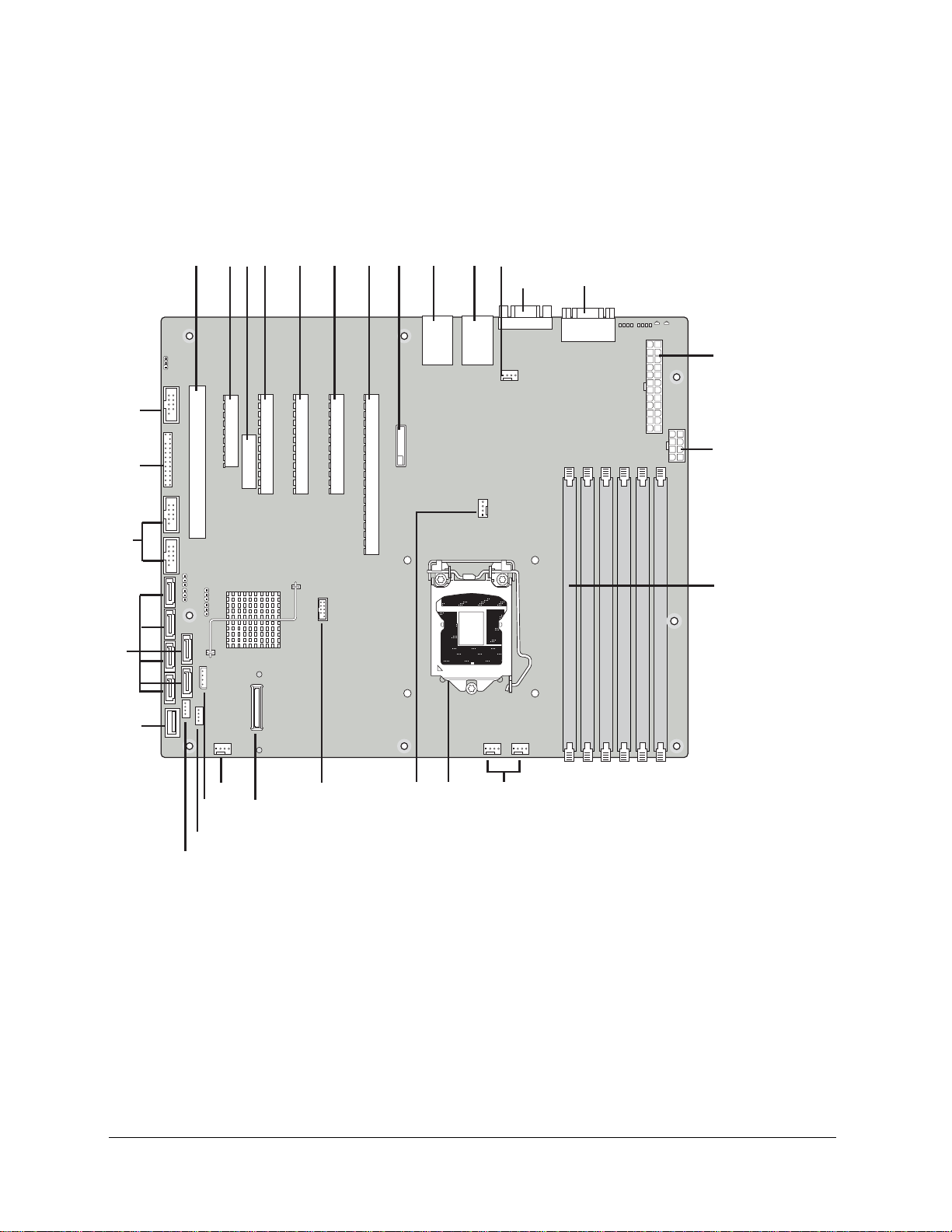
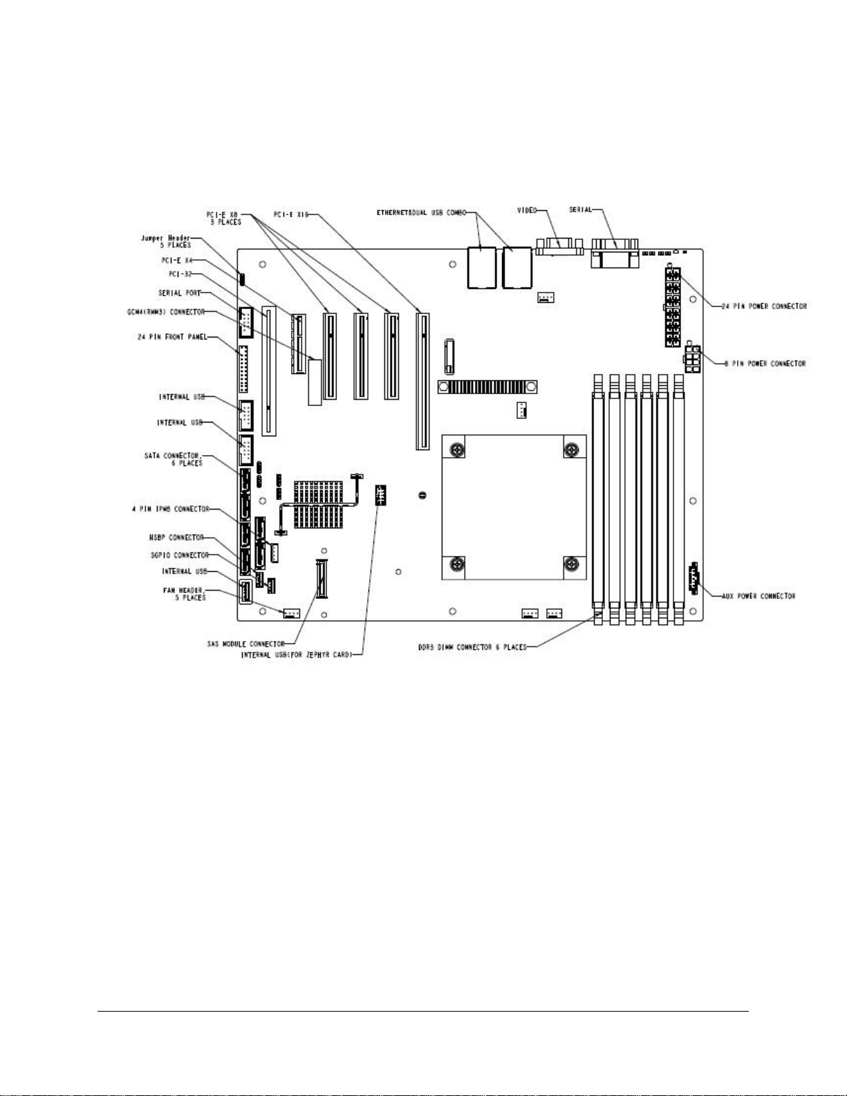
The following figure shows the board layout of the server board. Each connector and major
component is identified by a number or letter, and 2 provides the description.
DD
CC
BB
A
ABCDEFGH
J
I
K
LM
N
O
P
Z
V
W
X
Y
U
T
R
S
Q
AF003290
®
Figure 2. Intel
Server Board S3420GP Layout
Revision 1.0
4
Intel order number E65697-003
Page 19

IntelP®P Server Board S3420GP TPS Overview
Table 2. Major Board Components
A Slot 1, 32 Mbit/33 MHz PCI Q System FAN2 and System FAN 3
B Slot 2, PCI Express* Gen1 x1 (x4 connector)
(Intel Server Board S3420GPLX only)
C Intel RMM3 Connector(Intel Server Board S CPU Fan connector
S3420GPLX only)
D
Slot 3, PCI Express* Gen1 x4 (PCI Express* T USB SSD connector
Gen2 compliant)
E Slot 4, PCI Express* Gen2 x4 (x8 connector)
(x8 connector)( Intel
only)
F Slot 5. PCI Express* Gen2 x8 (x8 connector) V System FAN 1
G Slot 6, PCI Express* Gen2 x8 (x16 connector) W IPMB
H CMOS battery X SATA_SGPIO
I Ethernet and Dual USB COMBO Y HSBP
J Ethernet and Dual USB COMBO Z USB Floppy
K System FAN 4 AA Six SATA ports
L Video port BB Internal USB Connector
M External Serial port CC Front Panel Connector
N Main Power Connector DD Internal Serial Port
O CPU Power connector
P DIMM slots
Description Description
R CPU connector
®
Server Board
®
Server Board S3420GPLX
U SAS Module connector ( Intel
S3420GPLX only)
Revision 1.0
5
Intel order number E65697-003
Page 20
Overview IntelP®P Server Board S3420GP TPS
2.2.2 Intel® Server Board S3420GP Mechanical Drawings
Figure 3. Intel® Server Board S3420GP – Key Connector and LED Indicator IDENTIFICATION
Revision 1.0
6
Intel order number E65697-003
Page 21
IntelP®P Server Board S3420GP TPS Overview
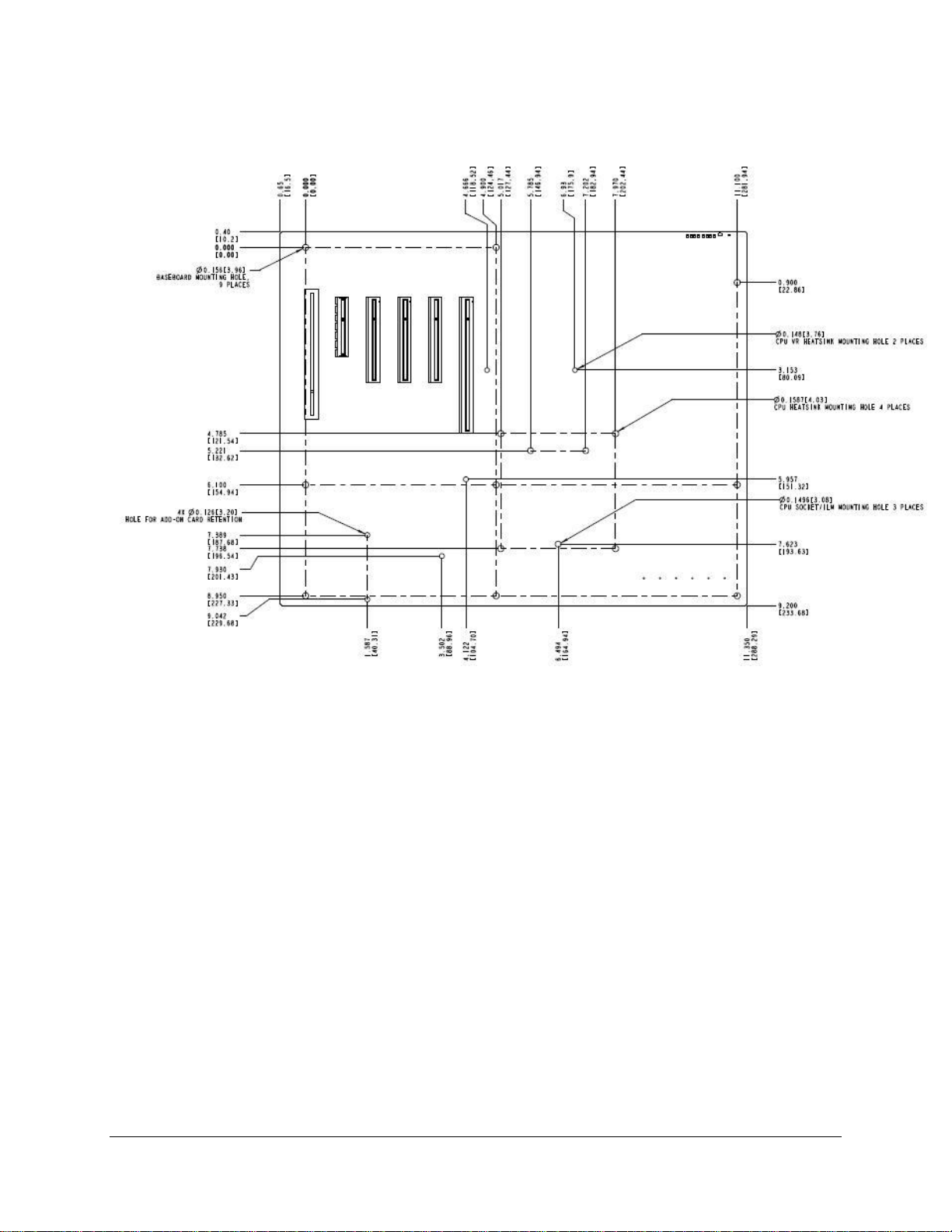
Figure 4. Intel® Server Board S3420GP – Hole and Component Positions
Revision 1.0
7
Intel order number E65697-003
Page 22
Overview IntelP®P Server Board S3420GP TPS
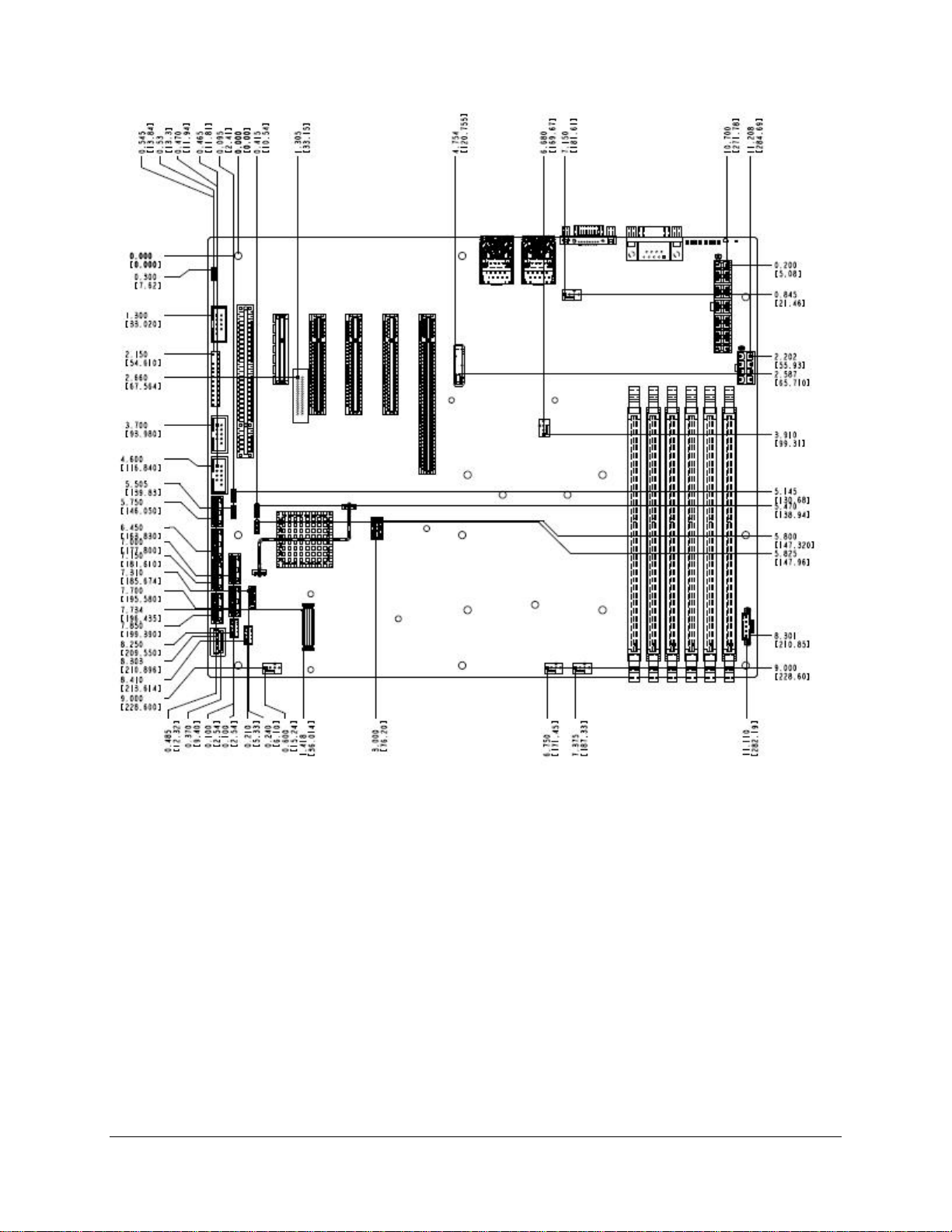
Figure 5. Intel
Revision 1.0
8
®
Server Board S3420GP – Major Connector Pin Location (1 of 2)
Intel order number E65697-003
Page 23
IntelP®P Server Board S3420GP TPS Overview
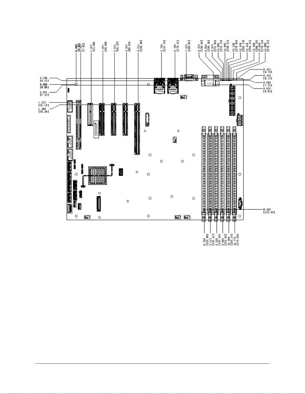
Figure 6. Intel® Server Board S3420GP –Major Connector Pin Location (2 of 2)
Revision 1.0
9
Intel order number E65697-003
Page 24
Overview IntelP®P Server Board S3420GP TPS
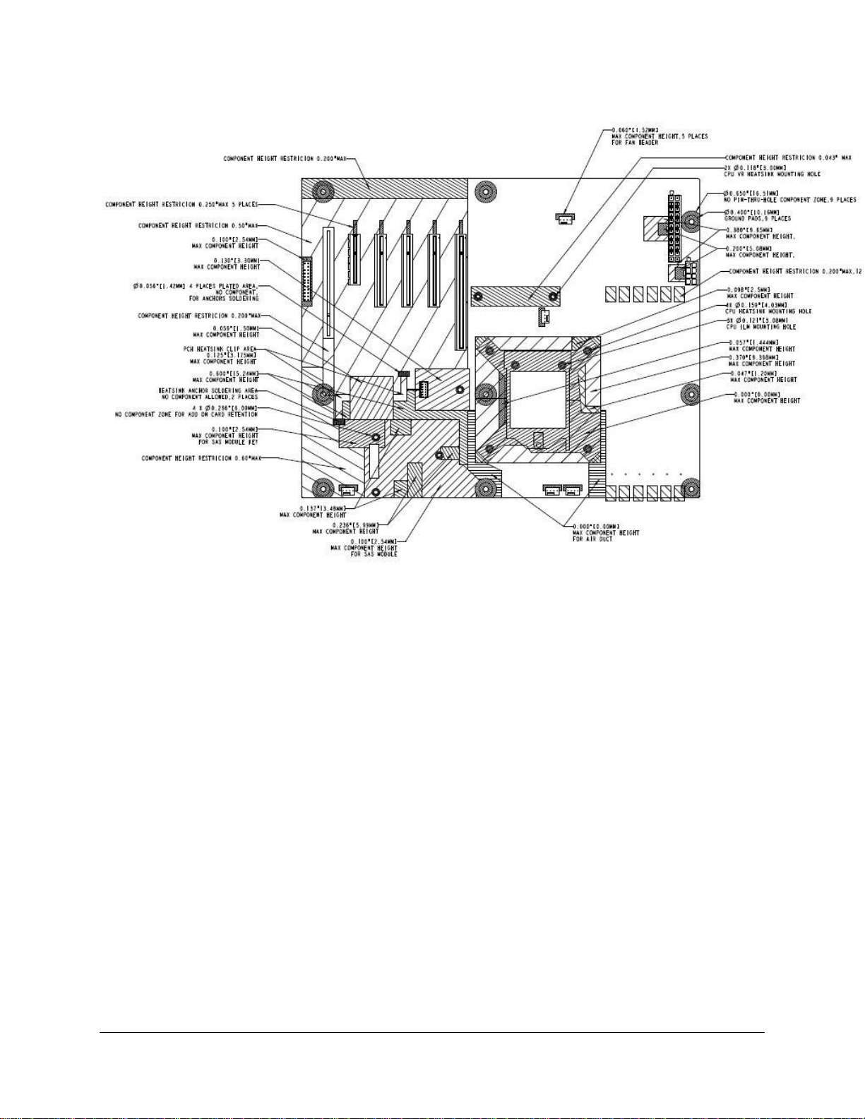
Figure 7. Intel® Server Board S3420GP – Primary Side Keepout Zone
Revision 1.0
10
Intel order number E65697-003
Page 25
IntelP®P Server Board S3420GP TPS Overview
Figure 8. Intel® Server Board S3420GP – Secondary Side Keepout Zone
Revision 1.0
11
Intel order number E65697-003
Page 26
Overview IntelP®P Server Board S3420GP TPS
2.2.3
The fol igure shows the layou
lowing f t of the rear I/O components for the server board.
Server Board Rear I/O Layout
A Serial Port A C NIC Port 1 (1 Gb) and Dual USB Port
Connector
B Video D NIC port 2 (1 Gb) and Dual USB Port
Connector
Figure 9. Intel® Server Board S3420GP Rear I/O Layout
12
Revision 1.0
Intel order number E65697-003
Page 27
IntelP®P Server Board S3420GP TPS Functional Architecture
3 nct. Fu ional Architecture
The architecture and design of the Intel® Server Board S3420GP is based on the Intel
Chipset. The chipset is designed for systems based on the Intel
®
Xeon® processor in the FC-
®
3420
LGA 1156 socket package. The chipset contains two main components:
Intel 3420 Chipset
PCI Express* switch (Intel
®
®
Server Board S3420GPLX only).
This chapter provides a high-level description of the functionality associated with each chipset
component and the architectural blocks that make up the server board.
ATX - 12" x 9.6"
4 unbuffered
or
6 registered
DIMMs
SERIAL 2
SERIAL 1
(x16 connector)
(x8 connector)
(x8 connector)
(x8 connector)
(x4 connector)
Slot 6
Slot 5
Slot 4
Slot 3
Slot 2
Slot 1
SAS
PCI
FLASHFLASH
SATA-II
6 onboard
S3420GPLX Block Diagram
PCIe Gen2 x8
Intel® Xeon
PCIe Gen2 x8
PCIe Gen2 x4
PCIe Gen2 x4
PCIe
Gen1
PCIe
N/C
Gen1
PCI32
SPI
2
(FP
headers)
x4
x1
SATA
612
(User Bay
headers)
ICH
G2PS
ICH1
9/
0
Intel® 3420
PCH
1
2
USB
Floppy
Header
PCIe Gen2 x8
x4 DMI Gen1
PCIe
Gen1
PCIe
Gen1
LPC
USB
3400
Gen1 x1 )
( PCIe
x1
82574L
x1
IBMC
USB
1.1
RMII
Zoar
USB
2.0
RMII
RMM3
DDR3 (Ch B)
®
DDR3 (Ch A)
Ch A Ch B
XDP0
82578DM
GbE
PHY
SPI
PORT 80
1
SPI
2
Z-U130
FLASHFLASH
DDR2
FLASH
USB2USB
GbE
GbE
BMC Boot
Flash
VIDEO
Notes:
1. Video integrated into BMC.
Figure agram For S3420GPLX 10. Intel® Server Board S3420GP Functional Block Di
Revision 1.0
Intel order number E65697-003
ejd
13
Page 28
Functional Architecture IntelP®P Server Board S3420GP TPS
(x16 ectoconn r)
(x8 to
(x8 connector)
Slot 6
Slot 5
Slot 3
Slot 1
PCI
FLASHFLASH
SATA-II
6 onboard
S3420GPLC Block Diagram
PCIe
Gen1
PCI32
SPI
headers)
x4
2
(FP
PCIe Gen2 x8connec r)
Intel® 3420
Chipset
612
SATA
2
(User Bay
headers)
PCIe Gen2 x8
Intel
3420
Chipset
1
USB
Floppy
Header
®
x4 DMI Gen1
PCIe
Gen1
PCIe
Gen1
LPC
USB
® ®
Intel Xeon
3400
Processor
( PCIe Gen1 x1 )
x1
82574
x1
IBMC
Zoar
USB
USB
1.1
2.0
RMII
XDP0
RMII
SPI
Z-U130
82578DM
1
GbE
PHY
PORT 80
DDR3 (Ch B)
DDR3 (Ch A)
FLASHFLASH
DDR2
FLASH
2
USB2USB
Ch A Ch B
GbE
GbE
BMC Boot SPI
Flash
VIDEO
Not
1. Video integrated into BMC.
SERIAL 1
es:
ATX - 12" x
4 unbuffered
or
6 registered
DIMMs
SERIAL 2
9.6"
ejd
®
Figure 11. I
ntel Server Board S3420GP Functional Block Diagram From S3420GPLC
<TBD>
Figure 12. Intel Server Board S3420GP Functional Block Diagram From S3420GPV
3.1
Processor Sub-System
The t
In el® Server Board S3420GP supports the following processor:
®
Intel
The Intel
based
3.1.1
The Intel
Nehale
FC-
Xeon
®
X rocessors processors are made up of multi-core processors
eon® 3400 Series p
on the 45 nm process technology.
Intel® Xeon® 3400 Processor
®
m-based processor cores.
®
Xeon 3400 Series processors highly integrated solution variant is composed of four
LGA 1156 socket package with 2.5 GT/s.
Up to 95 W Thermal Design Power (TDP); processors with higher TDP are not
®
®
3400 Processor series
supported.
14
Revision 1.0
Intel order number E65697-003
Page 29

IntelP®P Server Board S3420GP TPS Functional Architecture
The server
3.1.2 Intel Turbo Boost Technology
Inte Boost certain processors in the Intel® Xeon® Processor
l® Turbo Technology is featured on
3400 Series. Intel
processor to run fa
board does not support previous generations of the Intel
®
®
Turbo Boost Technology opportunistically and automatically allows the
ster than the marked frequency if the processor is operating below power,
®
Xeon® processors.
temperature, and current limits. This results in increased performance for both multi-threaded
and n
si gle-threaded workloads.
®
Intel
Turbo Boost Technology operation:
t operates under Operating System control – It is only entered when the
Turbo Boos
operating system requests the highest (P0) performance state.
Turbo Boost operation can be enabled or disabled by BIOS.
Turbo Boost converts any available power and thermal headroom into higher frequency
on active cores. At nominal marked processor frequency, many applications consume
less than the rated processor power draw.
Turbo Boost availability
Maximum Turbo Boost frequency depends on the number of active cores and varies by
is independent of the number of active cores.
processor configuration.
The amount of time the system spends in Turbo Boost operation depends on workload,
o
perating environment, and platform design.
®
If th o
e pr cessor supports the Intel
an o
ption to enable or disable this feature. The default state is enabled.
Turbo Boost Technology feature, the BIO
S Setup provides
3.1. (SMT)
3 Simultaneous Multithreading
Mos t ts
t In el® Xeon® processors support Simultaneous Multithreading (SMT). The BIOS detec
processors that support this feature and enables the feature during POST.
If the processor supports this feature, the BIOS Setup provides an option to enab
this The d
feature. efault is enabled.
3.1.4 Enhanced In
®
Xeon® processors support the Geyserville3 feature of the Enhanced Intel SpeedStep®
Intel
chnology. This feature changes the processor operating ratio and voltage similar to the
te
tel SpeedStep® Technology
le or disable
Thermal Monitor 1 (TM1) feature. The BIOS implements the Geyserville3 feature in conjunction
with the TM1 feature.
The BIOS enables a combination of TM1 and TM2 according to the
processor BIOS writer's guide.
3.2 Memory Subsystem
The Intel® Xeon® 3400 series processor has an Integrated Memory Controller (IMC) in its
package. Each Intel
memory. Each DDR3 channel in the IMC supports up to three DDR3 RDIMM slots or up to two
UDIMM slots. The DDR3 RDIMM frequency can be 800/1066/1333 MHz. DDR3 UDIMM
®
Xeon® 3400 series processor produces up to two DDR3 channels of
Revision 1.0
Intel order number E65697-003
15
Page 30

Functional Architecture IntelP®P Server Board S3420GP TPS
frequency can be 1066/1333 MHz. All RDIMMs and UDIMMs include ECC (Error Correction
Code) operation. Various speeds and memory technologies are supported.
RAS (Reliability, Availability, and Serviceability) is not supported on the Intel
®
Server Board
S3420GP.
3.2.1 Memory Sizing and Configuration
The Intel® Server Board S3420GP supports various memory module sizes and configurations.
These combinations of sizes and configurations are valid only for DDR3 DIMMs approved by
Intel Corporation.
S3420GP BIOS supports:
z DIMM sizes of 1 GB, 2 GB, 4 GB, and 8 GB.
z DIMMs composed of DRAM using 2 Gb technology.
z DRAMs organized as single rank, dual rank, or quad rank DIMMS.
z DIMM speeds of 800, 1066, or 1333 MT/s.
z Registered or Unregistered (unbuffered) DIMMs (RDIMMs or UDIMMs).
Note: UDIMMs should be ECC, and ma or may not have thermal sensors; RDIMMs must have y
ECC and must have thermal sensors.
S3420GP BIOS has the below limitations:
256 Mb technology, x4 DRAM on UDIMM, and quad rank UDIMM are NOT supported
x16 DRAM on UDIMM is not supported on combo routing
Memory suppliers not productizing native 800 ECC UDIMMs
Intel
256 Mb/512 Mb technology, x4 an
All channels in a system will run at
No mixing of registered and unbuffered DIMMs
®
Xeon® 3400 Series support all timings
d x16 DRAMs on RDIMM are NOT supported
the fastest common frequency
defined by JEDEC.
3.2.2 Post Error Codes
The range {0xE0 - 0xEF} of POST codes is used for memory errors in early POST. In late POST,
this range is used for reporting other system errors.
z 0xE8 - No Us
Diagnostic LED
z 0xE8 - Configuratio
the DIMM slot as if no
DIMM installed in the s
usable memo
z 0xEB - Memory Test E
memory channe
the BIOS emits a beep code and displays POST Diagnostic LED code 0xEB
momentarily d
able Memory Error: If no memory is available, the system emits POST
code 0xE8 and halts the system.
n Error: If a DDR3 DIMM has no SPD information, the BIOS treats
DDR3 DIMM is present on it. Therefore, if this is the only DDR3
ystem, the BIOS halts with POST Diagnostic LED code 0xE8 (no
ry) and halts the system.
rror: If a DDR3 DIMM or a set of DDR3 DIMMs on the same
l (row) fails HW Memory BIST but usable memory remains available,
uring the beeping and then continues POST. If all of the memory fails HW
16
Revision 1.0
Intel order number E65697-003
Page 31

IntelP®P Server Board S3420GP TPS Functional Architecture
Memory BIST, the system acts as if no memory is available, beeping and halting with
the POST Diagnostic LED code 0xE8 (No Usable Memory) displayed.
itialization process is unable to
z 0xEA - Channel Training Error: If the memory in
properly perform the DQ/DQS training on a memory channel, the BIOS emits a beep
code and displays POST Diagnostic LED code 0xEA momentarily during the beeping. If
there is usable memory in the system on other channels, POST memory initialization
continues. Otherwise, the system halts with POST Diagnostic LED code 0xEA staying
displayed.
z 0xED - Population Error: If the installed memory contains a mix of RDIMMs and
UDIMMs, the system halts with POST Diagnostic LED code 0xED.
z 0xEE - Mismatch Error: If more th
an two quad-ranked DIMMs are installed on any
channel in the system, the system halts with POST Diagnostic LED code 0xEE.
3.2.
3 Publishing System Memory
• The BIOS displays the Total M
disabled in the BIOS setup. This is
during POST, and is the sum of the
emory of the system during POST if Quiet Boot is
the total size of memory discovered by the BIOS
individual sizes of installed DDR3 DIMMs in the
system.
• The BIOS displays the Eff
ective Memory of the system in the BIOS Setup. The term
Effective Memory refers to the total size of all active DDR3 DIMMs (not disabled) and not
used as redundant units.
• The BIOS provides the total memory of the system in the main page of the BIOS setup.
This total is the same as the amount described by the first bullet in this section.
• If Quiet Boot is disabled, the BIOS displays the total system memory on the diagnos
tic
screen at the end of POST. This total is the same as the amount described by the first
bullet in this section.
• The BIOS provides the total amount of memory in the system.
3.2.3.1 Memory Reservation for Memory-mapped Functions
A region of size 40 MB of memory below 4 GB is always reserved for mapping chipset,
proces BIOS (flash) spaces as
sor, and memory-mapped I/O regions. This region appears as a
loss of memory to the operating system. In addition to this loss, the BIOS creates another
reserved region for memory-mapped PCIe functions, including a standard 64 MB or 256 MB of
standard PCI Express* MMIO configuration space.
If PAE is turned on in the operating
system, the operating system reclaims all these reserved
regions.
In addition to this memory reservation, the BIOS creates another reserved region for memorymapped PCI Express* functions, including a standard 64 MB or 256 MB of standard PCI
Express* Memory Mapped I/O (MMIO) configura
tion space. This is based on the selection of
Maximize Memory below 4 GB in the BIOS Setup.
If this is set to Enabled, the BIOS maximizes u
sage of memory below 4 GB for an operating
system without PAE capability by limiting PCI Express* Extended Configuration Space to 64
buses rather than the standard 256 buses. This is done using the MAX_BUS_NUMBER featur
Revision 1.0
Intel order number E65697-003
e
17
Page 32

Functional Architecture IntelP®P Server Board S3420GP TPS
offered by the Intel® S3420 I/O Hub and a variably-sized Memory Mapped I/O region for the PCI
Express* functions.
3.2.3.2 High-Memory Reclaim
When 4 GB or more o f physical memory is installed (physical memory is the memory installed
as DDR s), the reserved me
feature high-memory reclaim
3 DIMM mory is lost. However, the Intel
called , which allows the BIOS and operating system to remap the
lost physical memory into system memory above 4 GB (the system memory is the memor
®
3420 chipset provides a
y the
processor can see).
The BIOS always enables high-memory reclaim if it discovers installed physical memory equal
to or greater than 4 GB. For the operating system, the reclaimed memory is recoverable only if
the
PAE feature in the processor is supported and enabled. Most operating systems support
this feature. For details, see the relevant operating system manuals.
3.2.3.3 ECC Support
Onl C
y E C memory is supported on this platform.
3.2.4 Support for Mi
xed-speed Memory Modules
The BIOS supports memory modules of mixed speed by automatic selection of the lowest
common frequency of all memory modules (DDR3 DIMM). Each DDR3 DIMM adv
ertises its
lowest supported clock speed through the TCKMIN parameter in its Serial-presence Data (SPD).
The BIOS uses this information to arrive at the common lowest frequency that satisfies all
inst e
all d DDR3 DIMMs.
Thi e
s s ction describes the expected outcome on the installation of DDR3 DIMMs of different
equencies in the system for a given user-selected frequency. The following rules apply:
fr
If all three single-rank/dual-rank RDIMM slots are populated on a channel, the BIOS
forces a global common frequency of 800 MHz.
If two quad-rank RDIMM are popu
lated on one channel, the BIOS forces a global
common frequency of 800 MHz.
If one quad-rank RDIMM are populated on one channel, the BIOS forces a global
common frequency of 1066 MHz.
If a maximum of only two DIMM slots are populated in the system among all channels
and one or more DIMMs support DDR3 frequency greater than 1333 MH
z, the BIOS
forces a global common frequency of 1333 MHz.
3.2.5 Memory Map and Population Rules
The following nomenclature is followed for DIMM sockets:
®
Note: Intel
18
Server Board S3420GP may support up to three DIMM sockets per channel.
Table 3. Standard Platform DIMM Nomenclature
Channel A Channel B
A1 A2 A3 B1 B2 B3
Revision 1.0
Intel order number E65697-003
Page 33

IntelP®P Server Board S3420GP TPS Functional Architecture
3.2.5.1 TableMemory Subsystem Operating Frequency Determinat
ion
The rules for determining the operating frequency of the memory channels are simple, but not
necessarily straightforward. There are several limitin
on a channel and organization of the DIMM - that is, either single-rank (SR), dual-rank (D
g factors, including the number of DIMMs
R), or
quad-rank (QR):
The speed of the processor’s IMC is the maximum speed possible.
The speed of the slowest com
ponent – the slowest DIMM or the IMC – determines the
maximum frequency, subject to further limitations.
A single 1333-MHz DIMM (SR or DR) on a channel may run at full 1333-MHz speed.
If two SR/DR D
A single QR RDIMM on a channel is limited to 1066 MHz.
Two QR RDIMMs or a mix of QR + SR/DR on a channel is limite
IMMs are installed on a channel, the speed is limited to 1066 MHZ.
d to 800 MHz.
3.2.5.2 Memory Subsystem Nomenclature
1. DIMMs are organized into physical slots on DDR3 memo
ry channels that belong to
processor sockets.
2. The memory channels are identified as channels A, B.
®
3. For Intel
sockets (three DIMM sockets p
Xeon® 3400 Series, each socket can support a maximum of six DIMM
er channel), which can support a maximum of six
DIMM sockets.
4. The Intel
populated on the processor socket. It has an Integ
The IMC provides two DDR3
autonomous
5. The DIMM id
channel and the proc
the first sl
® ®
Xeon 3400 Series processor on the In
tel® Server Board S3420GP is
rated Memory Controller (IMC).
channels and groups DIMMs on the board into an
memory.
entifiers on the silkscreen on the board provide information about the
essor socket to which they belong. For example, DIMM_A1 is
ot on channel A.
3.2.5.3 Memory Upgrade Rules
Upgrading the system memory requires careful positioning of the DDR3 DIMMs based on the
follo in
w g factors:
Existing DDR3 DIMM population
DDR3 DIMM characteristics
Op
timization techniques used by the Intel® Nehalem processor to maximize memory
bandwidth
In the Independent Channel mode, all DDR3 channels operate independently. Slot-to-slot DIMM
matching is not required across channels (for example, A1 and B1 do not have to match each
other in terms of size, organization, and timing). DIMMs within a channel do not have to match
in terms of size and organization, but they operate in the minimal common frequency. Also,
Independent Channel mode can be used to support single DIMM configuration in channel A and
in the Single Channel mode.
Revision 1.0
Intel order number E65697-003
19
Page 34

Functional Architecture IntelP®P Server Board S3420GP TPS
Channel A Channel B
RDIMM
UDIMM
A1 A2 A3 B1 B2 B3
X
X X
X X X
X
X X
X X X X
X X
X X X X X
X X X X X X
X
X X
X
X X
X X
X
X
X X
X
X
X X
You must observe the following general rules when selecting and configuring memory to obtain
the best performance from the system.
1. DDR3 RDIMMs must always be populated using a fill-farthest method.
2. DDR3 UDIMMs must always be populated on DIMM A1/A2/B1/B2.
®
3. Intel
Xeon® 3400 Series Processors support either RDIMMs or UDIMMs.
4. RDIMM and UDIMM CANNOT be mixed.
5. The minimal memory set is {DIMMA1}.
6. DDR3 DIMMs on adjacent slots on the same channel do not need to be identical.
Each socket supports a maxim
use the Intel
®
3420 chipset support three slots per DDR3 channel, two DDR3 channels per
um of six slots. Standard Intel
socket, and only one socket is supported on the Intel
®
®
Server Bo
r boards and systems that
serve
ard S3420GP.
3.2.5.4 Memory Configuration Table
Table 4. Memory Configuration Table
This table defines half of the valid memory configurations. You can exchange Channel A DIMMs
with the DIMMs on Channel B to get another half.
20
Intel order number E65697-003
Revision 1.0
Page 35

IntelP®P Server Board S3420GP TPS Functional Architecture
3.3 Intel® 3420 Chipset PCH
The Intel® 3420 Chipset component is the Platform Controller Hub (PCH). The PCH is designed
for use with Intel
®
processor in a UP server platform. The role of the PCH in Intel® Server Board
S3420GP is to manage the flow of information between its eleven interfaces:
DMI interface to Processor
PCI Express* Int
PCI Interface
SATA I
nterface
USB Host Interface
SMBus Host Interface
SPI Interface
LPC interface to IBMC
JTAG interface
LAN interface
ACPI interface
3.4 I/O Sub
-system
erface
Intel® 3420 Chipset PCH provides extensive I/O support.
3.4.1 PCI Express Interface
Two diffe nfigurations on single board are depende
z
z Intel
z Intel
There is one 32-bit, 33-MHz 5-V PCI slot.
Compatibility with the PCI addressing model is maintained to ensure all existing applications
and drivers operate unchanged.
The PCI Express* configuration uses standard mechanisms as defined in the PCI Plug-andPlay specification. The initial recovered clock speed of 1.25 GHz results in 2.5 Gb/s/direction,
which provides a 250-MB/s communications channel in each direction (500 MB/s total). This is
close to twice the data rate of classic PCI. The fact that 8b/10b encoding is used accounts for
the 250 MB/s where quick calculations would imply 300 MB/s. The external graphics ports
support 5.0 GT/s speed as well. Operating at 5.0 GT/s results in twice as much bandwidth per
lane as compared to 2.5 GT/s operation.
rent PCI-E co nt on different board SKUs:
Intel® Server Board S3420GPLX
One PCI-E X16 slot connected to the PCI-E ports of CPU. Two PCI-E x8 slots and one SAS
module connected to PCI-E ports
connected to the PCI-E ports of PCH.
®
Server Board S3420GPLC
One PCI-E X16 slot and o
E x8 slot connected to the PCI-E ports of PCH.
®
Server Board S3420GPV
>
<TBD
ne PCI-E X8 slot connected to the PCI-E ports of CPU. One PCI-
of PCIe switch. One PCI-E X8 slot and one PCI-E x4 slot
Revision 1.0
Intel order number E65697-003
21
Page 36

Functional Architecture IntelP®P Server Board S3420GP TPS
When operating with two PCI Express* controllers, each controller can operate at either 2.5
GT/s or 5.0 GT/s. The PCI Express* architecture is specified in three layers: Transaction Layer,
Data Link Layer, and Physical Layer. The partitioning in the component is not necessarily along
these same boundarie
s.
3.4.2 Serial ATA Support
The Int 0 Chipset has two integrated
DMA operation on up to six ports and supports data transfer rates of up to 3.0 GB/s (300 MB/s).
The SATA controller contains two
AHCI mode using memory space.
el® 342 SATA host controllers that support independent
modes of operation – a legacy mode using I/O space and an
Softwa ses legacy mode does not have AH
re that u CI capabilities. The Intel
®
3420 Chipset
supports the Serial ATA Specification, Revision 1.0a. The Ibex Peak also supports several
optional sections of the Serial ATA II: Extensions to Serial ATA 1.0 Specification, Revision 1.0
(AHCI support is required for some elements).
3.4.2.1 Intel
The Intel
AHCI (see above for details on
RAID capability provides high-p
ports of PCH. Matrix RAID support is provided to allow multiple RAID levels to be combin
®
Matrix Storage Technology
® ®
3420 Chipset provides support for Intel Matrix Storage Technology, providing both
AHCI) and integrated RAID functionality. The industry leading
erformance RAID 0, 1, 5, and 10 functionality on up to six SATA
ed on
a single set of hard drives, such as RAID 0 and RAID 1 on two disks. Other RAID features
include hot spare support, SMART alerting, and RAID 0 autos replace. Software components
include an Option ROM for pre-boot configuration and boot functionality, a Microsoft Windows*
compatible driver, and a user interface to configure and manage the RAID capability of the
®
Intel
3420 Chipset.
3.4.3 USB 2.0 Support
On the Intel® 3420 Chipset, the USB controller functionality is provided by the dual EHCI
controllers with an interface for up to ten USB 2.0 ports. All ports a
and low-speed capable.
Four external connectors are located on the back edge of the server board.
Two internal 2x5 header (J1E2 and J1D1) are pro
vided, each supporting two optional
USB 2.0 ports.
One port on internal vertical connector to support NIC.
One port on 1x4pin (J1J2) on-board header to support floppy.
re high-speed, full-speed,
3.4.3.1
Native USB Support
During the power-on self test (POST), the BIOS initializes and configures the USB subsystem.
The BIO ble low o ice
S is capa of initializing and using the fol ing types f USB dev s.
USB Specification-compliant keyboards
USB Specification-compliant mouse
USB Specification-compliant storage devices that utilize bulk-only transport mechanism
USB devices are scanned to determine if they are required for booting.
22
Intel order number E65697-003
Revision 1.0
Page 37

IntelP®P Server Board S3420GP TPS Functional Architecture
The BIOS supports USB 2.0 mode of operation, and as such supports USB 1.1 and USB 2.0
compliant devices and host controllers.
During the p
US e
B d vices and a short beep is emitted to indicate such an action. For example, if a USB
re-boot phase, the BIOS automatically supports the hot addition and hot removal of
device is hot plugged, the BIOS detects the device insertion, initializes the device, and makes it
available to the user. During POST, when the USB controller is initialized, it emits a short beep
for c
ea h USB device plugged into the system as they were all just “hot added”.
Onl n
y o -board USB controllers are initialized by BIOS. This does not prevent the operating
system
3.4.3.2
from supporting any available USB controllers including add-in cards.
Legacy USB Support
The BIOS supports PS/2 emulation of USB keyboards and mouse. During POST, the BIOS
initializes and configures the root hub ports and searches for a keyboard and/or a mouse on the
USB hub and then enables the devices that are recognized.
3.5 Optional
The Intel® Server Board S3420G vides a llation
of an op
tional Intel
Entry RAID Module AX SASMOD is detected, I
switches to the SAS Mezzanine slot. The option
SASMOD includes a SAS1064e controller that supports x4 PCI Express* link widths and
AXX4
®
SAS
®
Intel D Module AXX4SASMOD
SAS Entry RAI
PLX pro SAS Mezzanine slot (J2H1) for the insta
Entry R ule AX S
AID Mod
X4
X4SASMOD. Once the optional Intel
the x4 PCI Express* links from the PC
al Intel
®
SAS Entry RA
ID Module
®
SA
is a single-function PCI Express* end-point device.
The SAS controller supports the SAS protocol as described in the Serial Attached SCSI
Standard, version 1.0, and also supports SAS 1.1 features. A 32-bit external memory bus off th
SAS1064e controller provides an interface for Fla
sh ROM and NVSRAM (Non-volatile Static
Random Access Memory) devices.
The optional Intel
®
SAS Entry RAID Module AXX4SASMOD provid
es four SAS connectors that
support up to four hard drives with a non-expander backplane or up to eight hard drives with an
expander backplane.
e
3.6 Integrated Baseboard Management Controller
The ServerEngines* LLC Pilot II Integrated BMC is provided by an embedded ARM9 controller
and associated peripheral functionality that is required for IPMI-based server managem
Firmware usage of these hardware features
The following is a summary of the Integrated
Serv E
er ngines* LLC Pilot II Integrated BMC:
250 MHz 32-bit ARM9 Processor
Memory Management Unit (MMU)
Two 10/100 Ethernet Controllers with NC-SI support
16-bit DDR2 667 MHz interface
Dedicated RTC
Revision 1.0
Intel order number E65697-003
is platform-dependant.
BMC management hardware features used by the
ent.
23
Page 38

Functional Architecture IntelP®P Server Board S3420GP TPS
12 10-bit ADCs
Eight Fan Tachometers
Four PWMs
Battery-backed Chassis Intrusion I/O Register
JTAG Master
Six I
General-purpose I/O Ports (16 direct, 64 serial)
2
C interfaces
Additionally, the ServerEngines* Pilot II part integrates a super I/O module with the following
features:
KCS/BT Interface
Two 16C5
50 Serial Ports
Serial IRQ Support
12 GPIO Ports (shared with BMC)
LPC to SPI Bridge
SMI and PME Support
The Pilot II contains an integrated KVMS subsystem and graphics controller with the following
features:
USB 2.0 f
USB 1.1 interface for legacy PS/2 to USB bridging
or keyboard, mouse, and storage devices
Hardware Video Compression for text and graphics
Hardware encryption
2D Graphics Acceleration
DDR2 g
raphics memory interface
Up to 1600x1200 pixel resolution
PCI Express* x
1 support
24
Revision 1.0
Intel order number E65697-003
Page 39

IntelP®P Server Board S3420GP TPS Functional Architecture
Integrated BMC Block Diagram
Interrupt
Controller
ARM926EJ-S
16K D & I
Cache
RTC &
General Purpose
TImers (3)
BMC & KVMS Subsystem
UART (3) GPIO
LPC
Interface
To Host
LPC
Interface
LPC to SPI
Flash Bridge
BMC & KVMS Subsystem Graphics Subsystem
Fan Tach (12)
PWM (4)
UART
(3)
Watchdog
Timer
I2C
(6)
KCS
BT &
Mailboxes
ADC
Thermal
Ethernet
MAC with
RMII (2)
System
Wakeup
Control
Real Time Clock
Interface
(external RTC)
USB
to Host
USB 1.1
&
USB 2.0
Crypto
Accelerator
Code
Memory
LPC Master,
JTAG Master,
& SPI FLash
DDR-II
16-bit
Memory
Controller
Graphics
Controller
JTAG
er
Mast
DDR-II
(up to
667MHz)
Video
Output
PCIe x1
Interface
Figure 13. Integrated BMC Hardware
3.6.1 Integrated BMC Embedded LAN Channel
The Integrated BMC hardware includes two dedicated 10/100 network interfaces.
Interface 1:
be shared with the host. Only one NIC may be enabled for management traffic at any time. To
change the NIC enabled for management traffic, please use the “Write LAN Channel Port” OEM
IPMI command. The default active interface is port 1 (NIC1).
Interface 2: This interface is available from the optional RMM3 which is a dedicated
management NIC that is not shared with the host.
For these channels, support can be enabled for IPMI-over-LAN and DHCP.
For security reasons, embedded LAN channels have the following default settings:
IP Address: Static
All users disabled
This interface is available from either of the available NIC ports in system that can
3.6.2 Optional RMM3 Advanced Management Board
On the Intel
management board serves two purposes:
Revision 1.0
®
Server Board S3420GPLX provides RMM3 module. RMM3 advanced
Intel order number E65697-003
25
Page 40

Functional Architecture IntelP®P Server Board S3420GP TPS
• Give the customer the option to add a dedica
ted management 100 Mbit LAN interface to
the product.
• Provide additional flash space, enabling the Advanced Management functions t
o support
WS-MAN and CIMON.
ble 5. Optional RMM3 Advanced Management Board Features
Ta
Feature Description
KVM Redirection Remote console access via keyboard, video, and mouse redirection over LAN.
USB Media Redirection Remote USB media access over LAN.
WS-MAN Full SMASH profiles for WS-MAN based consoles.
3.6.3 Serial Ports
The server board provides two serial ports: an external DB9 serial port connector and an
internal DH-10 serial header.
The rear DB9 serial A port is a fully-functional serial port that can support any standard serial
device.
The Serial B port is an optional port accessed through a 9-pin internal DH-10 header (J1B1).
You can use a standard DH-10 to DB9 cable to direct serial A port to the rear of a chassis. The
serial B interface follows the standard RS-232 pin-out as defined in the following table.
Table 6. Serial B Header (J1B1) Pin-out
Pin Signal Name Serial Port B Header Pin-out
1 DCD
2 DSR
3 RX
4 RTS
5 TX
6 CTS
7 DTR
3.6.4
8 RI
9 GND
Floppy Disk Controller
The server board does not support a floppy disk controller interface. However, the system BIOS
rec
ognizes USB floppy devices.
3.6.5
Keyboard and Mouse Support
The server board does not support PS/2 interface keyboards and mouse. However, the system
BIO r
S ecognizes USB specification-compliant keyboard and mouse.
26
Intel order number E65697-003
Revision 1.0
Page 41

IntelP®P Server Board S3420GP TPS Functional Architecture
3.6.6
Wake-up Control
The super I/O contains functionality that allows various events to power on and power off the
system
3.7
.
Video Support
The server board includes a video controller in an on-board Server Engines* Integrated
Baseboard Management Controller along with 64 MB of video DDR2 SDRAM. The SVGA
subsystem supports a variety of modes, up to 1600 x 1200 resolution in 8 / 16 / 32 bpp modes
under 2D. It also supports both CRT and LCD monitors up to a 100 Hz vertical refresh rate.
The video is accessed using a standard 15-pin VGA connector found on the back edge of the
server board. The on-board video controller can be disabled using the BIOS Setup utility or
when an add-in video card is detected. The system BIOS provides the option for dual-video
oper
ation when an add-in video card is configured in the system.
3.7
.1 Video Modes
The t
in egrated video controller supports all standard IBM VGA modes. The following table
sho
ws the 2D modes supported for both CRT and LCD.
Table 7. Video Modes
2D Video Mode Support 2D Mode Refresh Rate (Hz)
8 bpp 16 bpp 32 bpp
640x480 60, 72, 75, 85, 90, 100, 120, 160, 200 Supported Supported Supported
800x600 60, 70, 72, 75, 85, 90, 100, 120,160 Supported Supported Supported
1024x768 60, 70, 72, 75,85,90,100 Supported Supported Supported
1152x864 43,47,60,70,75,80,85 Supported Supported Supported
1280x1024 60,70,74,75 Supported Supported Supported
1600x1200 52 Supported Supported Supported
3.7
.2 Dual Video
The BIOS supports both single-video and dual-video modes. The dual-video mode is disabled
by d a
ef ult.
ller is
In the single mode (dual monitor video = disabled), the on-board video contro
disabled when an add-in video card is detected.
r is disabled when an add-in video card is
In single mode, the onboard video controlle
detected.
In dual mode, the onboard video controller is enabled and is the primary video device.
The external video card is allocated resources and is considered the secondary video
device.
bled.
When KVM is enabled in iBMC FW, dual video is ena
Table 8. Dual Video Modes
Revision 1.0
Intel order number E65697-003
27
Page 42

Functional Architecture IntelP®P Server Board S3420GP TPS
Enabled
Onboard Video
Dual Monitor Video
3.8 ller (NIC)
The 3420GPLX and S3420GPLC support two network interfaces, One is
provided from the onboard Intel
onb r
The t
the b
3.8.1 GigE Controller 82574L
Network Interface Contro
®
Intel Server Board S
oa d Intel
In el
on oard Intel
®
82578 Gigabit N
®
Server Board S3420GPV only suppo
®
82574L GbE PCI Express*
Disabled
Enabled If enabled, both the onboard video controller and
Disabled
®
82574L GbE PCI Express network controller; the other is the
etwork controller.
The 82574 family (82574L and 82574IT) are single, compact, low-power components th
a fully-integrated Gigabit Ethernet Media Access Control (MAC) and Physical Layer (PH
The 82574 uses the PCI Express* architecture and provides a si
Onboard video controller.
Warning: System video is completely disabled if
this option is disabled and an add-in video
adapter is not installed.
an add-in video adapter are enabled for system
video. The onboard video controller becomes
the primary video device.
rts one network interface, which is provided from
network controller.
at offer
Y) port.
ngle-port implementation in a
relatively small area so it can be used for server and client configurations as a LAN on
Motherboard (LOM) design.
External interfaces provided on the 82574:
• PCIe Rev. 2.0 (2.5 GHz) x1
• MDI (Copper) standard IEEE 802.3 Ethernet interface for 1000BASE-T, 100BASET
and 10BASE-T applications (802.3, 802.3u, and 8 2.3ab)
0
• NC-SI or SMBus connection to a Manageability Controller (MC)
• EEE 1149.1 JTAG (note
that BSDL testing is NOT supported)
X,
3.8.2 GigE PHY 82578DM
The 82578 is a single port Gigabit Ethernet Physical Layer Transceiver (PHY). It connects to the
Media Access Controller (MAC) through a dedicated interconnect. The 82578DM supports
operation at 1000/100/10 Mb/s data rates. The PHY circuitry provides a standard IEEE 802.3
Ethernet interface for 1000BASE-T, 100BASE-TX, and 10BASE-T a
and 802.3ab).
The 82578 operates with the Platform Controller Hub (PCH) chipset that incorporates the MAC
The 82578 interfaces with its MAC through two interfaces: PCIe-based and SMBus. T
(main) interface is used for all link speeds when the system is in an active state (S0) while the
SMBus is used only when the system is in a low power state (Sx). In SMBus mode, the link
speed is reduced to 10 Mb/s. The PCIe interface incorporates two aspects: a PCIe SerDes
(electrically) and a custom logic protocol.
3.8 efinition
.3 MAC Address D
Each Intel Server Board S3420GPLX has the following four MAC addresses assigned to it at
®
the Intel factory:
NIC 1 MAC address
28
Intel order number E65697-003
Revision 1.0
pplications (802.3, 802.3u,
.
he PCIe
Page 43

IntelP®P Server Board S3420GP TPS Functional Architecture
NIC 2 MAC address – Assigned the NIC 1 MAC address +1
Integrated BMC LAN Channel MAC address – Assigned the NIC 1 MAC address +2
Intel
®
Remote Management Module 3 (Intel® RMM3) MAC address – Assigned the NIC 1
MAC address +3
Each Intel
®
Server Board S3420GPLC has the followin
g three MAC addresses assigned to it at
the Intel factory:
NIC 1 MAC address
NIC 2 MAC address – Assigned the NI
Integrated BMC LAN Channel MAC address – Assigned the NIC 1 MAC address +2
®
Each Intel
®
Intel
Server Board S3420GPV has the following two MAC addresses ass
factory:
C 1 MAC address +1
igned to it at the
<TBD>
3.9 Intel® I/O Acceleration Technolgy 2 (Intel® I/OAT2)
The Intel 3420 chipset series platforms do not support Intel
® ®
I/O Acceleration Technology.
3.9.1
Dir C
ect ache Access (DCA) is not supported on Intel® Xeon® 3400 Series processors.
3.1
0 Intel® Virtualization Technology for Directed I/O (Intel® VT-d)
The Int
Tec o
components that support the virtualization of platforms based on Intel
el® 3420 chipset provides hardware support for implementation of Intel® Virtualization
hn logy with Directed I/O (Intel
Direct Cache Access (DCA)
®
VT-d). Intel VT-d Technology
ists of technology
cons
®
Architecture Processor.
Intel VT-d Technology enables multiple operating systems and applications to run in dependent
partitions. A partition behaves like a virtual machine (VM) and provides isolation and protection
acr
oss partitions. Each partition is allocated its own subset of host physical memory.
The t
sha g
disable
Note: If the setup options are changed to enable or disable the Virtualization Technology sett
®
In el
Virtualization Technology is designed to support multiple software environments
rin the same hardware resources. The Intel
®
Virtualization Technology can be enabled or
d in the BIOS setup. The default behavior is disabled.
ing
in the processor, the user must perform an AC power cycle for the changes to take effect.
Revision 1.0
Intel order number E65697-003
29
Page 44

Platform Management IntelP®P Server Board S3420GP TPS
4. Platform Management
The platform management subsystem is based on the Integrated BMC features of the
ServerEngines* Pilot II. The onboard platform management subsystem consists of
communication buses, sensors, system BIOS, and server management
diagram provides an overview of the Server Management Bus (SMBUS) architecture used o
this server board.
firmware. The following
n
Figure 14. Server Management Bus (SMBUS) Block Diagram
4.1 Feature Support
4.1.1 IPMI 2.0 Features
Integrated Baseboard Management Controller (Integrated BMC).
IPMI Watchdog timer.
Messaging support, including command bridging and user/session support.
Chassis device functionality, including power/reset control and BIOS boot flags support.
Event receiver device: The Integrated BMC receives and processes events from other
platform subsystems.
Field replaceable unit (FRU) inventory device functionality: The Integrated BMC supports
access to system FRU devices using IPMI FRU commands.
30
Intel order number E65697-003
Revision 1.0
Page 45

IntelP®P Server Board S3420GP TPS Platform Management
System event log (SEL) device functionality: The Integrated BMC supports and provides
ccess to a SEL.
a
Sensor device record (SDR) repository device functionality: The Integrated BMC
supports storage and access of syst
Sensor device and sensor scanning/monitoring: The
management of sensors. It polls sensors to monitor
em SDRs.
Integrated BMC provides IPMI
and report system health.
IPMI interfaces.
o Host interfaces include system management software (SMS) with receive
message queue support and server managemen
t mode (SMM).
o Terminal mode serial interface
IPMB interface o
o LAN interface that supports the IPMI-over-L
Serial-over-LAN
(SOL)
ACPI state synchronization: The Integrated
BMC tracks ACPI state changes provided by
AN protocol (RMCP, RMCP+)
the BIOS.
Integrated Baseboard Management Controller (Integrated BMC) self test: The Integrated
BMC performs initialization and run-time self tests, and makes results available to
external entities.
For more information, refer to the IPMI 2.0 Specification.
4.1.2 Non-IPMI Features
The Integrated BMC supports the following non-IPMI features. This list does not preclude
support for future enhancements or additions.
In-circuit Integrated BMC firmware update.
Fault resilient booting (FRB): FRB2 is supported by the watchdog timer functionality
Chassis intrusion detection and chassis intrusion cable presence detection.
Basic fan control using TControl version 2 SDRs.
Acoustic management: Su
Signal testing support: The Integrated Baseboard Management Controller (Integrated
BMC) provides test commands for setting and getting platform signal states.
The Integrated Baseboard Management Controller (Integrated BMC) generates
diagnostic beep codes for fault conditions.
System GUID storage and retrieval.
Front panel management: The Integrated Baseboard Management Controller (Integra
BMC) controls the system status LED and chassis ID LED. It supports secure lockout
certain front panel functionality and monitors button presses. The c
turned on using a front panel button or a command.
Power state retention
Power fault analysis
®
Intel
Light-Guided Diagnostics
pport for multiple fan profiles.
hassis ID LED is
ted
of
Revision 1.0
Intel order number E65697-003
31
Page 46

Platform Management IntelP®P Server Board S3420GP TPS
Power unit management: Support for power unit sensor. The Integrated Baseboard
anagement Controller (Integrated BMC) handles power-good dropout conditions.
M
DIMM temperature monitoring: New sensors and
improved acoustic management using
c
losed-loop fan control algorithm taking into account DIMM temperature readings.
Address Resolution Protocol (ARP): The Integrated BMC sends and responds to ARPs
(
supported on embedded NICs)
Dynamic Host Configuration Protocol (DHCP): The Integrated BMC performs DHCP
(supported on embedded NICs).
Platf nvironment control inte
orm e rface (PECI) thermal management support.
E-mail alerting
Embedded web server
Integrated KVM
Integrated Remote Media Redirection
Lightweight Directory Authentication Protocol (LDAP) support
4.2 O anced Management Feature Support
This section e
ptional Adv
xplains the
advanced management features supported by the Integrated
Baseboard Management Controller (Integrated BMC) firmware.
4.2.1 Enabling Advanced Management Features
The Integrated BMC enab
presence of the Intel
RMM3, the advanced ures are dormant. Only the Intel
RMM3 module interface.
4.2.1.1 Intel
The Intel
The dedicated
®
RMM3 provides the Integrated BMC with an additional dedicated network interface.
interface consumes its own LAN channel. Additionally, the Intel
additional flash storage for advanced features like Web Services for Management (WS-MAN).
les the advanced management features only when it detects the
®
Rem tel
ote Management Module 3 (Intel® RMM3) card. Without the In
feat
®
RMM3
®
Server Board S3420GPLX has
®
RMM3 provides
®
a
4.2.2 Keyboard, Video, Mouse (KVM) Redirection
The Integrated BMC firmware supports keyboard, video, and mouse redi
feature is available remotely from the embedded web server as a Java applet. This feature is
enabled only when the Intel
Environment (JRE) version 5.0 or later to run th
®
RMM3 is present
. The client system must have a Java Runtime
e KVM or media redirection applets.
rection over LAN. This
4.2.2.1 Keyboard and Mouse
The keyboard and mouse are emulated by the Integrated BMC as USB human interface devices
4.2.2.2 Video
Video output from the KVM subsystem
is equivalent to the video output on the local console.
Video redirection is available after video is initialized by the system BIOS. The KVM video
resolution and refresh rates will always match the values set in the operating system.
32
Intel order number E65697-003
Revision 1.0
.
Page 47

IntelP®P Server Board S3420GP TPS Platform Management
4.2.2.3 Availa
bility
Up to two remote KVM sessions are supported. The default inactivity timeout is 30 minutes;
howeve
not disa
remote KVM is not deactiv
r, chan
this can
b l system
le the loca
be ged through the embedded web server. Remote KVM activation does
keyboard, video, or mouse. Unless the feature is disabled locally,
ated by local system input.
KVM sessions persist across system reset but not across an AC power loss.
4.2.3 Media Redirection
The embedded web server provides a Java applet to enable remote media redirection. This may
be used in conjunction with
The media redirection feat a
remote IDE or USB CD-RO r.
Once mounted, the remote ng system
ministr ers to e
ad ators or us install software (including operating systems), copy files, update th
BIOS, and so forth, or boot the server from this device.
e follow ilities a
Th ing capab re supported:
The operation of remotely mounted devices is independent of the local devices on the
se emote
rver. Both r and local devices are usable in parallel
Ei D-RO e
se
rver.
It boo
is possible to t all supported operating systems from the remotely mounted device
and to boot from disk IMAGE (*.IMG) and CD-ROM or DVD-ROM ISO files. Refer to the
Tested/supported Operating System List for more information.
It mo
is possible to unt at least two devices concurrently.
The mounted devic
system and BIOS i
The mounted device shows up in the BIOS boot order and it is possible to change the
BIOS boot order to boot from this remote device.
It is possible to install an operating system
present) using the remotely mounted device. This may also require the use of KVM-r to
configure the opera
If either a virtual IDE or vir
virtual IDE and virtual flopp
sin dev
the remote KVM feature or as a standalone applet.
ure is intended to allow system administrators or users to mount
M, floppy drive, or a USB flash disk as a remote device to the serve
device appears just like a local device to the server, allowi
M, floppy) or USB devices can be mounted as a rem ther IDE (C
ote device to th
e is visible to (and useable by) the managed system’s operating
n both pre-boot and post-boot states.
on a bare metal server (no operating system
ting system during install.
tual floppy device is remotely attached during system boot, both
y are presented as bootable devices. It is not possible to present
ice type to the system BIOS. only a gle mounted
4.2.3.1 Availability
The default inactivity timeout is 30 minutes, but may be changed through the embedded web
server.
Media redirection sessions
Revision 1.0
persist across system reset but not across an AC power loss.
Intel order number E65697-003
33
Page 48

Platform Management IntelP®P Server Board S3420GP TPS
4.2.4 Web Services for Management (WS-MAN)
The Integrated BMC firmware supports the Web Services for Management (WS-MAN)
specification, version 1.0.
4.2.5 Local Directory Aut
The Integrated BMC firmware supports the Local Directory Authentication Protocol (LDAP)
protoco er authentication. Note that IPMI users/passw
supported over LDAP.
4.2.6 Embedde
The te
authentication is handled by IPMI user names and passwords. Base functionality for the
embedd
The e
See p
l for us ords and sessions are not
d Webserver
In grated BMC provides an embedded web server for out-of-band management. User
ed web server includes:
Power Control – Limited control based on IPMI user privilege.
Sensor Reading – Limited access based on IPMI user privilege.
SEL Reading – Limited access based on IPMI user privilege.
KVM/Media Redirection – Limited access based on IPMI user privilege. Only available
w
hen the Intel
IPMI User Management – Limited access based on IPMI user privilege.
w b server is available on all enabled LAN channels.
A pendix B for Integrated BMC core sensors.
®
RMM3 is present.
hentication Protocol (LDAP)
4.3 M
Intel Management Engine is tied to e
firmware includes the following applications:
anagement Engine (ME)
ssential platform functionality. This Management Engine
Platform Clocks – Tune PCH clock silicon to the parameters of a specific board,
configure clocks at run time, power management clocks.
Thermal Report – ME FW reports thermal and power information available only on PECI
to host accessible registers / Embedded Controller via SMBus.
34
Revision 1.0
Intel order number E65697-003
Page 49

IntelP®P Server Board S3420GP TPS BIOS User Interface
5. BIOS User Interface
5.1 n
Logo / Diagnostic Scree
The ostic Screen displays in o
logo / Diagn ne of two forms:
z If Quiet Bo
Quiet Boot setup. If the logo disp
de the logo and display the d
z If a log ROM or if Quiet
ot is enabled in the BIOS setup, a logo splash screen displays. By default,
is enabled in the BIOS lays during POST, press <Esc>
iagnostic screen. to hi
o is not present in the flash Boot is disabled in the system
configuration, the summary and diagnostic screen displays.
The diagnostic screen displays the following information:
z BIOS ID
z Platform
z Total memory of all installed DD
Processor information (Intel branded string, speed, and number of physical processor
z
identified
z Keyboard )
Mouse devices detected (if plugged in)
z
name
detected (Total size R3 DIMMs)
)
s detected (if plugged in
5.2 BIOS Boot Popup Menu
The BIOS Boot Specification (BBS) provides for a Boot Popup Menu invoked by pressing the
F6> key during POST. The BBS popup menu displays all available boot devices. The list order
<
in the popup menu is not the same as the boot order in the BIOS setup; it simply lists the
bootable devices from which the system can be booted.
When a User Password or Administrator Password is active in Setup, the password is to access
the Boot Popup Menu.
5.3 BIOS Setup utility
The BIOS setup utility is a text-based utility that allows the user to c
view curre n evices. The Setup utility
nt settings and environme t information for the platform d
controls the platform’s built-in devices, boot manager, and error ma
The BIOS setup interface consists of a number of pages or screens. Each page contains
information or links to other pages. The advanced tab in Setup displays a list of general
categories a
s links. These links lead to pages containing a specific category’s configuration.
The following sections describe the look and behavior for platform s
5.3.1 Operation
The BIOS a
Revision 1.0
Setup has the following fe tures:
Intel order number E65697-003
onfigure the system and
nager.
etup.
35
Page 50

BIOS User Interface IntelP®P Server Board S3420GP TPS
z Localization - The BIOS Setup uses the Unicode standard and is capable of displaying
setup forms all languages urrently included in the Unico
in c de standard. The Intel
®
server board BIOS is only available in English.
z Console Redirection - The BIOS Setup is functional through
console redirection over
various terminal emulation standards. This may limit some functionality for compatibility
(for example, color usage or some keys or key sequences or support of pointing
evices).
d
5.3.1.1 Setup Page Layo
ut
The setup page layout is sectioned into functional areas. Each occupies a specific area of the
screen and has icated fu lity. The following table lists a describes each functional
ded nctiona nd
area.
Table 9. BIOS Setup Page Layout
Functional Area Description
Title Bar The title bar and displays the title of the form
(page) the u ing. It may also display navigational information.
Setup Item List The Setup I nd informational items. Each item in the
list occupies the left column of the screen.
A Setu may also open a new window w
on the board
Item Specific Help Area The Item Specific Help area is located on the right side of the screen and contains
help text for lp information may include the meaning
and usage o of the options, and so forth.
Keyboard Command Bar The Keyboard Command Bar is located at the bottom right of the screen and
continuously ial keys and navigation keys. displays help for keyboard spec
is located at the top of the screen
ser is currently view
tem List is a set of controllable a
p Item ith more options for that functionality
.
the highlighted Setup Item. He
f the item, allowable values, effects
5.3.1.2 Entering BIOS Setup
To enter the BIOS Setup, press the F2 fun
ction key during boot time when the OEM or Intel logo
displays. The following message displays on the diagnostics screen and under the Quiet Boot
logo screen:
Press <F2> to enter setup
When the
Setup is entered, the Main screen displays. However, serious errors cause the
system to display the Error Manager screen instead of the Main screen.
5.3.1.3 Keyboard Commands
The bottom right portion of the Setup screen provides a list of commands used to navigate
through the Setup utility. These commands display at all times.
Each Setup menu page contains a number of features. Each feature is associated with a value
field except those used for informative purposes. Each value field contains configurable
parameters. Depending on the security option chosen and, in effect, by the password, a menu
feature’s value may or may not be changed. If a value cannot be changed, its field is made
inaccessible and appears grayed out.
Revision 1.0
36
Intel order number E65697-003
Page 51

IntelP®P Server Board S3420GP TPS BIOS User Interface
Table 10. BIOS Setup: Keyboard Command Bar
Key Option Description
<Enter> Execute The <Enter> key is used to activate sub-menus when the selected feature is a sub-
Command menu,
<Esc sc> key provides a mechanism for backing out of any field. When the <Esc>
> Exit The <E
↑
↓
↔
<Tab> Se ab> key is used to an be used
- C minus key on the keyp ent item to the
+ Change Value The plus key on the keypa lue of the current menu item to
<F9> Setup Defaults F9> causes the to display:
<F10> Save and Exit Pressing <F10> causes the following message to display:
Select Item
Select Item The down arrow is used to select the next value in a menu item’s option list, or a
Select Menu keys are used to move betw
lect Field The <T move between fields. For example, <Tab> c
hange Value The ad is used to change the value of the curr
or to display a pick list if a selected option has a value field, or to select a
-field for multi-valued features like time and date. If a pick list is displayed, the
sub
<Enter>
the focus to the parent
key is pressed w
menu is re-entered.
When the <Esc> key is pressed in any sub-menu, the parent menu is re-entered.
When the <Esc> key is pressed in a
displayed and the user is asked whe
selected and the <Enter> key is pressed, or if the <Esc> key is pressed, the user is
returned to where they were before <Esc> was pressed, without affecting any
existing settings. If “Yes” is selected and the <Enter> key is pressed, the setup is
exited and the BIOS returns to the main System Options M
The up arrow is used to select the previous value in a pick list, or the previous
option in a menu item's option list. The selected item must then be activated by
pressing the <Enter> key.
<Enter> key.
The left and right arrow
The keys have no affect if a sub-menu or pick list is display
to move from hours to min time item in the main menu.
previous value. This key s gh the values in the associated pick list
without displaying the ist.
the nex rolls through the values in the associated pi
displaying the full list. On 1 panese keyboards, the plus key has a different
s y on the other keyboards, but will have
Pressing < following
If “Yes” is highlighted and <Enter> is pressed, all Setup fields are set to their
default values. If “No” is highlighted and <Enter> is pressed, or if the <Esc> key is
pressed, the use
affecting any exis
If “Yes” is highlighted and <Enter> is pressed, all changes are saved and the Setup
is exited. If “No” is highlighted and <Enter> is pressed, or the <Esc> key is pressed,
the user is returned to where they were before <F10> was pressed without affecting
any existing values.
key selects the currently highlighted item, undoes the pick list, and returns
menu.
hile editing any field or selecting features of a menu, the parent
ny major menu, the exit confirmation window is
ther changes can be discarded. If “No” is
enu screen.
pressing the value field’s pick list. The selected item must then be activated by
een the major menu pages.
ed.
utes in the
crolls throu
full l
d is used to change the va
t value. This key sc ck list without
06-key Ja
can code than the plus ke the same effect.
Load Optimized Defaults?
Yes No
r is returned to where they were before <F9> was pressed without
ting field values.
Save configuration and reset?
Yes No
Revision 1.0
Intel order number E65697-003
37
Page 52

BIOS User Interface IntelP®P Server Board S3420GP TPS
5.3.1.4 Menu Selection Bar
The Menu Selection Bar is located at the top of the BIOS Setup Utility screen. It displays the
major menu selections available to the user. By using the left and right arrow keys, the user can
select the menus listed here. Some menus are hidden and become available by scrolling off the
left or right of the current selections.
5.3.2 tform Setup tility Screens
Server Pla U
The following sections describe the screens available for the configuration of a server platform.
In these sections, tables are used to describe the contents of each screen. These tables follow
the following guidelines:
z ptions, and He document the text and
The Setup Item, O
lp Text columns in the tables
values displayed on the BIOS Setup screens.
z In the Options column, the default values display in bold. These values are not
displayed in bold on tup screen; the
the BIOS Se bold text in this document serves as a
reference point.
z vides n where it may be helpful. This
The Comments column pro additional informatio
information does not display on the BIOS Setup screens.
z
Information enclosed in angular brackets (< >) in the screen shots identifies text that
can vary, depending on the op
tion ample, <Current Date> is replaced
(s) installed. For ex
by the actual current date.
z ed in square br bles identifies areas where the
Information enclo
u r must type in
z hanged ime), the system requires a save
and reboot to take pla
according to the bo m the last boot.
s ackets ([ ]) in the ta
ad of s vided option.
is cWhenever information
ce. Pressin he changes and boots the system
electing from a prose text inste
(except Date and T
g <ESC> discards t
ot order set fro
5.3.2.1 Main Screen
The Main screen is the first screen displayed when the BIOS Setup is entered, unless an error
occurred. If an error occurred, the Error Manager screen displays instead.
Revision 1.0
38
Intel order number E65697-003
Page 53

IntelP®P Server Board S3420GP TPS BIOS User Interface
Advance
d
Security Server Management Boot Options Boot Manager
Main
Logged in as <Administrator or User>
Platform ID
<Platform Identification String>
System BIOS
Version SXXXX.86B.xx.yy.zzzz
Build Date <MM/DD/YYYY>
Memory
Total Memory <How much memory is installed>
Quiet Boot Enabled/Disabled
POST Error Pause Enabled/Disabled
System Date <Current Date>
System Time <Current Time>
Figure 15. y
Setup Utility – Main Screen Displa
Table 11.
Setup Item Options Help Text Comments
Logged in as
Platform ID
System BIOS
Version
Build Date
Memory
Setup Utility – Main Screen Fields
Information only. Displays
password level that setup is
running
With no
Admini
Informa
Platform ID.
LX S
LC S
V SK
Information only. Displays the
current BIOS version.
xx = major version
yy = minor version
zzzz = build number
Informa
current B
i Administrator or User.
n:
passwords set,
strator is the default mode.
tion only. Displays the
KU 3420GPLX
: S
KU: S3420GPLC
U: S3420GPV
tion only. Displays the
IOS build date.
Revision 1.0
39
Intel order number E65697-003
Page 54

BIOS User Interface IntelP®P Server Board S3420GP TPS
Setup Item Options Help Text Comments
Size
Quiet Boot
POST Error Pause Enabled
System Date [Day of week
System Time [HH:MM:SS] System Time has configurable
Enabled
Disabled
Disabled
MM/DD/YYYY]
[Enabled] – Display the logo screen
during POST.
[Disabled] – Display the diagnostic
screen during POST.
[Enabled] – Go to the Error
Manager for critical PO
[Disabled] – Attempt to boot and do
not go to the Error Man
critical POST errors.
System Date has configurable
fields for Month, Day, and Year.
Use [Enter] or [Tab] key
next field.
the
Use [+] or [-] key to modify the
selected field.
fields for Hours, Minutes, and
Seconds.
Hours are in 24-hour format.
Use [Enter] or [Tab] key to select
the next field.
Use [+] or [-] key to modify the
selected field.
ST errors.
ager for
to select
Informa
total phy
the syste
physical l
memory
installed
If
option takes the system to the error
manag
major
er
thi
tion only. Displays the
sical memory installed in
m, in MB or GB. The term
memory indicates the tota
discovered in the form of
DDR3 DIMMs.
enabled, the POST Error Pause
e o review the errors when
r t
er rs occur. Minor and fatal
ro
ror displays are not affected by
s setting.
5.3.2.2 Advanced Screen
The Advanced screen provides an access point to configure several options. On this screen, the
user selects the option they want to configure. Configurations are performed on the selected
screen, and not directly on the Advanced screen.
To access this screen from the Main screen, press the right arrow until the Advanced screen is
chosen.
Revision 1.0
40
Intel order number E65697-003
Page 55

IntelP®P Server Board S3420GP TPS BIOS User Interface
Advance
d
Sec rity u Server Management Boot Options Boot Manager
Main
► Processor Configuration
► Memory Configuration
► Mass Storage Controller Configuration
► Serial Port Configuration
► USB Configuration
► PCI Configuration
► System Acoustic and Performance Configuration
Figure 16. Setup
Utility – Advanced Screen Display
Table 12. Setup Utility – Advanced Screen Display Fields
Setup Item Help Text
Processor Configuration View/Configure processor information and
Memory Configuration View/Configure memory information and
Mass Storage Controller Configuration View/Configure mass storage controller
Serial and
Port Configuration View/Configure serial port information
USB Configuration
PCI Configuration
System Acoustic and Performance View/Configure system acoustic and
Configuration performance information and settings.
settings.
settings.
information and settings.
settings.
View/Configure USB information and
settings.
View/Configure PCI information and
settings.
5.3.2.2.1 Processor Scre
en
The Processor screen allows the user to view the processor core frequency, system bus
frequency, and to enable or disable several processor options. This screen also allows the user
to view info pe
To access this screen from the
Revision 1.0
cific processor. rmation about a s
Main screen, select Advanced > Processor.
41
Intel order number E65697-003
Page 56

BIOS User Interface IntelP®P Server Board S3420GP TPS
Advanced
Processor Configuration
Processor Socket CPU 1
Processor ID <CPUID>
Processor Frequency <Proc Freq>
Microcode Revision <Rev data>
L1 Cache RAM Size of Cache
L2 Cache RAM
L3 Cache RAM
Size of Cache
Size of Cache
Processor 1 Version <ID string from Processor 1>
Current QPI Link Speed <Slow / Fast >
QPI Link Frequency <Unknown GT/s / 4.8 GT/s / 5.866 GT/s / 6.4 GT/s>
Intel® Turbo Boost Technology
Enabled / Disabled
Enhanced Intel SpeedStep® Tech Enabled / Disabled
Intel® Hyper-Threading Technology Enabled / Disabled
Core Multi-Processing All / 1 / 2
Exe te Disabcu le Bit Enabled / Disabled
Intel® Virtualization Technology Enabled/ Disabled
®
Intel VT for Directed I/O
Enabled/ Disabled
EnaInterrupt Remapping bled / Disabled
Coherency Support Enabled/ Disabled
ATS Support Enabled / Disabled
Pass-through DMA Support Enabled / Disabled
Hardware Prefetcher Ena isabled bled / D
Adjacent Cache Line Prefetch Enabled / Disabled
Figure 17. Setup Utility – Processor Configuration Screen Display
Table 13. Setup Utility – Processor Configuration Screen Fields
Setup Item Options Help Text Comments
Processor ID
Processor Frequency
Core Frequency
Revision 1.0
42
Information onl
CPUID.
Information only. Current
Information on
at cessor are
which the pro
cu .
rrently running
y. Processor
e processor. frequency of th
ly. Frequency
Intel order number E65697-003
Page 57

IntelP®P Server Board S3420GP TPS BIOS User Interface
Setup Item Options Help Text Comments
Microcode Revision
the loaded microcode.
L1 Cache RAM
L2 C
ache RAM
L3 Cache RAM
Processor Version
Current QPI Link Speed
QPI Link Frequency
Intel® Turbo Boost
Technology
Enhanced Intel
SpeedStep
®
Technology
Intel® Hyper-Threading
Tech
nology
Core Multi-Processing
Ena
bled
Disabled
Enabled
Disabled
Enabled
Dis
abled
All
1
2
Execute Disable Bit
®
Intel
Virtualization
Tech
nology
Ena
Dis
Ena
Dis
bled
abled
bled
abled
Ena Enable/Disable Intel
®
Intel
Virtualization
Tec
hnology for Directed
bled
Disabled
I/O
Interrupt Remapping
Enabled
Disabled
®
Turbo Boost Technology allows
Int
el
pr ease its
ocessor to automatically incr
fre r,
quency if it is running below powe
tem ns.
perature, and current specificatio
En
hanced Intel SpeedStep
all adjust
ows the system to dynamically
®
T
the
echnology
processor voltage and core frequency, which
can result in decreased average power
co ge heat
nsumption and decreased avera
pr
oduction.
Co OS
ntact your OS vendor regarding
su
pport of this feature.
®
echnology allows multithreaded
HT T
Int
el
are applications to execute thread
softw
s in
parallel within the processor.
Contact your OS vendor regarding OS
support of this feature.
Enable 1, 2 or All cores of installed
processor packages.
Execute Disable Bit can help prevent c
classes of malicious buffer overflow att
Contact y
our OS vendor regarding OS
ertain
acks.
support of this feature.
®
Virtualization Technology allows a
Intel
platform to run multiple operating sy ms
and applications in independent partitio
No e: A change to this option requires t
t
em to be powered off and then bac
stsy k on
ste
ns.
he
before the setting takes effect.
®
Virtualization
echnology for Directed I/O.
T
Report the I/O device assignment to VMM
through DMAR ACPI Tables
®
Enable/Disable Intel
VT-d Interrupt
Remapping support.
Information only
Processor L1 Cache
Information only. Size
Processor L2 Cache
Information only
Processor L3 Cache
Information only. ID
from the Processor.
Information only. Current
speed that the QPI Link is
using.
Information only. Cu
frequency that the QPI Link is
using.
This option is only visible if all
processor in the system
support Intel
®
Turbo Boost
Technology.
Only visible when Intel®
Virtualization Technology for
cted I/O is enabled. Dire
ion of Information only. Revis
. Size of the
.
of the
. Size of the
.
string
rrent
Revision 1.0
Intel order number E65697-003
43
Page 58

BIOS User Interface IntelP®P Server Board S3420GP TPS
Setup Item Options Help Text Comments
Coherency Support Enable/Disable Intel® VT-d Coherency
ATS Support
Pass-through DMA
Support
Hardware Prefetcher
Adjacent Cache Line
Prefetch
Enabled
Disabled
Enabled
Disabled
Enabled
Disabled
Enabled
Disabled
Enabled
Disabled
support.
®
Enable/Disable Intel
Transl upport.
ation Services (ATS) s
Enable
/Disable Intel
DMA s
upport.
Hardwa
prefetc ssor(s).
Note: M
system performance.
[Enabled] - Cache lines are fetched in pairs
(even line + odd line).
[Disabled] - Only the current cache line
required is fetched.
Note: Modifying this setting may affect
system performance.
re Prefetcher is a speculative
h unit within the proce
odifying this setting may affect
VT-d Address
®
VT-d Pass-throu
gh
Only visible when Intel®
Virtualization Technology for
Directed I/O is enabled.
Only visible when Intel®
Virtualization Technology for
Directed I/O is enabled.
Only visible when Intel
Virtualization Technology for
Directed I/O is enabled.
®
5.3.2.2.2 M
emory Screen
The Memory screen allows the user to view details about the system memory DDR3 DIMMs
installed. This screen also allows the user to open the Configure Memory RAS and Performance
screen.
To access this rom ain scr y.
screen f the M een, select Advanced > Memor
Revision 1.0
44
Intel order number E65697-003
Page 59

IntelP®P Server Board S3420GP TPS BIOS User Interface
Advanced
Memory Configuration
Total Memory <Total Physical Memory Installed in System>
Effective Memory <Total Effective Memory>
Current Configuration <Independent >
Current Memory Speed <Speed that installed memory is running at.>
►
DIMM Information
DIMM_A1 Install d/Disabled/Spare Unit ed/Not Installed/Faile
DIMM_A2 Installed/Not Installed/Failed/Disabled/Spare Unit
DIMM_A3 Installed/Not Installed/Failed/Disabled/Spare Unit
InstallDIMM_B1 ed/Not Installed/Failed/Disabled/Spare Unit
DIMM_B2 Installed/Not Installed/Failed/Disabled/Spare Unit
DIMM_B3 Installed/Not Installed/Failed/Disabled/Spare Unit
Figure 18. Setup Utility – Memory Configuration Screen Display
Table 14. Setup Utility – Memory Configuration Screen Fields
Setup Item Comments
Total Memory
Effective Mem
Current Config
ory
uration
Information only. The amount of memory availabl
in the form of installed DDR3 DIMMs in units of MB
Information only. The amount of memory availa
operating system in MB or GB.
The Effective Memory is the difference between th
Memory and th
RAS redundancy and SMRAM. This differenc
all DDR3 DIMMs that failed
disabled by the BIOS during memory discovery p
memory configuration.
Information only. Display
Independent Mode: System memory is con
performance and efficiency and no RAS
Sparing Mode: Sy
optimal effective m
e sum of all memory reserved for internal usage,
s one of the following:
stem memory is configured for
emory.
e in the system
or GB.
bl to the
e
e Total Physical
e incl
udes the sum of
Memory BIST during P ere
is enabled.
OST, or w
hase to optimize
figured l
for optima
RAS with
Revision 1.0
Intel order number E65697-003
45
Page 60

BIOS User Interface IntelP®P Server Board S3420GP TPS
Setup Item Comments
Current Memo
Speed
DIMM_ XY MM socket present on the board.
ry
Information only. Displays the speed the mem
Displays the state of each DI
Each DIMM socket field reflects one of the following possible
states:
Installed: There is a DDR3 DIMM installed in t slot.
Not Installed: There is no DDR3 DIMM install
Disabled: The DDR3 DIMM installed in this slot w
the BIOS to optimize memory configuration.
Failed: The DDR3 DIMM installed in this slot is fau
malfunctioning.
Spare Unit: The DDR3 DIMM is functioning as a s
memory RAS purposes.
Note: X denotes the Channel Identifier and Y deno
Identifier within the Channel.
ory
is running at.
his
ed in
this slot.
a
s disabled by
lty /
pare unit for
te the DIMM
5.3.2.2.3 Mass Storage Controller Screen
he Mass Storage screen allows the user to configure the SATA/SAS controller when it is
T
present on the baseboard, midplane, or backplane of an Intel system.
To access this screen from the Main menu, select Advanced > Mass Storage.
Advanced
Mass Storage Controller Configuration
Intel® Entry SAS RAID Module Enabled / Disabled
Configure Intel® Entry SAS RAID Module LSI ® Integrated RAID / Intel® ESRTII
Onboard SATA Controller Enabled / Disabled
Configure SATA Mode RAID
► SATA Port 0 Not Installed/<Drive Info.>
► SATA Port 1 Not Installed/<Drive Info.>
► SATA Port 2 Not Installed/<Drive Info.>
► SATA Port 3 Not Installed/<Drive Info.>
► SATA Port 4 Not Installed/<Drive Info.>
► SATA Port 5 Not Installed/<Drive Info.>
ENHANCED / COMPATIBILITY / AHCI / SW
Figure 19. Setup Utility – Mass Storage Controller Configuration Screen Display
Table 15. Setup Utility – Mass Storage Controller Configuration Screen Fields
Setup Item Options Help Text Comments
Revision 1.0
46
Intel order number E65697-003
Page 61

IntelP®P Server Board S3420GP TPS BIOS User Interface
Setup Item Options Help Text Comments
®
Intel AID
Entry SAS R
Module Entry RAID Module
Configure Intel® Entry
SAS RAID Module
Enabled
Disabled
LSI® Inte
RAID
Intel
®
ES
grated
R
TII
Enabled or Disable the Intel
®
Integrated RAID - Supports
LSI
RAID 0, RAID 1, and RAID 1e, as
well as IT (JBOD) mode;
® ®
Intel
ESRTII - Intel Embedded
Server RAID Tech
supports RAID 0,
RAID 1, RAID
10.
Onboard SATA
Controller
SATA Mode
Enabled
Disabled
ENHANCED
bi
Compati
lity
AHCI
SW RAID
Onboard Serial ATA (SATA)
er.
controll
[ENHANCED] - Supports up to 6
SATA ports with IDE Native
Mode.
[COMPATIBILITY] - Supports up
to 4 SATA po
rts[0/1/2/3] with IDE
Legacy mode and 2 SATA
ports[4/5] with IDE Native Mode.
[AHCI] - Supports all SATA ports
using the Advanced Host
Controller Interface.
[SW RAID] - Supports
configuration of SATA ports for
RAID via RAID configuration
software.
®
Intel
Matrix RAID Technology
with Software RAID level
and 5.
SATA Port 0 < Not Inst
alled /
Drive
information>
SATA Port 1 < Not In
st ed /
all
Drive
informat n>
SATA Port 2 nstalled /
< Not I
io
Drive
information>
SATA Port < Not Installed /
3
Drive
information>
SATA Port 4 < Not Installed /
Drive
information>
SATA Port 5 < Not Installed /
Drive
information>
®
SAS
nology II, which
s 0/1/10
Unavailable if the SAS Module
(AXX4SASMOD) is not present.
is option is not
Note:
Th
lable on some models.
avai
Unavailable if the SAS Module
X4 ASMOD) is disabled or
(AX
S
t present
no
Note: This option is not
availab
le on some models.
DisappA ears when the Onboard
SAT Controller is disabled.
Information only. This field is
unavai
lable when RAID Mode is
enable
d.
Inform
ation only. This field is
unavai
lable when RAID Mode is
enable
d.
Inform
ation only. This field is
unavailable when RAID Mode is
enabled.
Informa
unavailable w
tion only. This field is
hen RAID Mode is
enabled.
Information only. This field is
unavailable when RAID Mode is
enabled.
Information only. This fie
ld is
unavailable when RAID Mode is
enabled.
5.3.2.2.4 Serial Ports Screen
The Serial Ports screen allows the user to configure the Serial A [COM 1] and Serial B [COM2]
ports.
To access this screen from the Main screen, select Advanced > Serial Port.
Revision 1.0
Intel order number E65697-003
47
Page 62

BIOS User Interface IntelP®P Server Board S3420GP TPS
Advanced
Serial Port Configuration
Enabled/Disabled Serial A Enable
s 3F8h / 2F8h / 3E8h / 2E8h Addres
3 or 4 IRQ
Serial B Enable Enabled/Disabled
Address 3F8h / 2F8h / 3E8h / 2E8h
IRQ 3 or 4
Figure 20. Setup Utility – Serial Port Configuration Screen Display
Table 16. Setup Utility – Serial Ports Configuration Screen Fields
Setup Item Options Help Text
Serial A
Enable
Address
IRQ 3
Serial B
Enable
Address 3F8h
IRQ 3 4 Select Serial port B interrupt request (IRQ).
Enabled
Disabled
3F8h
2F8h
3E8h
2E8h
4
Enabl
ed
Disabled
2F8h
3E8h
2E8h
Enable or Disable Serial port A.
Select Serial port A base I/O address.
Enable or Disable Serial port B.
Select Serial port B base I/O address.
upt request (IRQ) line. Select Serial port A interr
2.5 uratio
5.3.2. USB Config n Screen
The USB Conf reen a ntroller op
To access this guration.
Revision 1.0
48
iguration sc llows the user to configure the USB co tions.
ain screen, select Advanced > USB Confi screen from the M
Intel order number E65697-003
Page 63

IntelP®P Server Board S3420GP TPS BIOS User Interface
Advanced
USB Configuration
Detected USB Devices
<Total USB Devices in System>
USB Controller Enabled / Disabled
Legacy USB Support Enabled / Disabled / Auto
Port 60/64 Emulation Enabled / Disabled
Make USB Devices Non-Bootable Enabled / Disabled
USB Mass Storage Device Configuration
/ 2 se0 seconds / 3010 seconds conds / 40
Device R eset timeout seconds
Mass Storage Devices:
<Mass storage devices one line/device> Auto / Floppy/Forced FDD/Hard Disk/CD-ROM
EnableUSB 2.0 controller d / Disabled
Figure 21. Setup Utility – USB Controller Configuration Screen Display
Table 17. Setup Utility – USB Controller Configuration Screen Fields
Setup Item Options Help Text Comments
Detected USB
Devices
USB Controller
Legacy USB
Support
Port 60
Emulation
Make USB
Devices NonBootable
Information only. Shows the number
of USB devices in the system.
Enabled
Disabled
Enabled
Disabled
Auto
Enabled
Disabled
Enabled
Disabled
[Enabled] - All onboard USB controllers are turned on and
accessible by the OS.
[Disabled] - All onboard USB controllers are turned off and
inaccessible by the OS.
USB device boot support and PS/2 emulation for USB
keyboard and USB mouse devices.
[Auto] - Legacy USB support is enabled if a USB device is
attached.
h emulation support.
Note: This may
support when using an OS that is USB unaw
Exclude USB i
[Enabled] - This removes all USB Mass Storage devices
as Boot options.
[Disabled] - This allows all USB Mass Storage devices as
Boot options.
be needed for legacy USB keyboard
n Boot Table.
are.
Grayed
disabled.
disabled.
Grayed out if the USB
disabled.
out if the USB Controller is
troller is /64 I/O port 60h/64 Grayed out if the USB Con
Controller is
Revision 1.0
Intel order number E65697-003
49
Page 64

BIOS User Interface IntelP®P Server Board S3420GP TPS
Setup Item Options Help Text Comments
Device
Reset 10 sec
timeout
One line for each
mass storage
device in system
USB 2.0
controll
er
20 sec
30 sec
40 sec
Auto
Floppy
Forced FDD
Hard Dis
CD-ROM
Enabled
Disabled
k
USB Mass e device Start Unit command timeou
Setting to a larger
storage device to be ready, if needed.
[Auto] - USB devic B are emulated as
floppies.
[Forced FDD] - HD
FDD (e.g., e).
Onboard
Contact y
feature.
Storag t.
value provides more time for a mass
es less than 530 M
D formatted drive are emulated as a
ZIP driv
USB por .
our OS v
ts are enabled to support USB 2.0 mode
endor regarding OS support of this
Grayed out if the USB Controll
disabled.
Hidden if no USB Mass storage
devices are installed.
Grayed out if the USB Controller is
disabled.
This setup screen can show
maximum of eight devices on this
screen. If more than eight devices
are installed in the system
Devices Enabled shows the
count, but only displays the fi
eight devices here.
Grayed out if the USB Controller is
disabled.
er is
a
, the USB
correct
rst
.3.2.2.6 PCI Screen
5
The PCI Screen allows the user to configure the PCI add-in cards, onboard NIC controllers, and
video op
tions.
To access this screen from the Main screen, select Advanced > PCI.
Advanced
PCI Configuration
Maximize Memory below 4GB Enabled / Disabled
Memory Mapped I/O above 4GB Enabled / Disabled
Onboard Video Enabled / Disabled
Dual Monitor Video Enabled / Disabled
Onboard NIC1 ROM Enabled / Disabled
Onboard NIC2 ROM Enabled / Disabled
Onboard NIC iSCSI ROM Enabled / Disabled
NIC 1 MAC Address <MAC #>
NIC 2 MAC Address <MAC #>
Figure 22. Setup Utility – PCI Configuration Screen Display
Revision 1.0
50
Intel order number E65697-003
Page 65

IntelP®P Server Board S3420GP TPS BIOS User Interface
Table 18. Setup Utility – PCI Configuration Screen Fields
Setup Item Options Help Text Comments
Ma mize Memory
xi
bel
ow 4GB
Memory
abo
ve 4GB
Onboard Video
Du bled. o controller and
al Monitor Video Enabled If en
On
board NIC1 ROM
On
board NIC2 ROM
Onboard NIC
ROM
NIC 1 MAC Address d
NIC 2 MAC Address try
iSCSI Enabled
Enabled
abled
Dis
Enabled
Disabled
Enabled
Disabled
Disabled
Enabled
Disabled
bled
Ena
Disabled
Disabled
No entry
allowe
No en
allowed
If enabled. the BIOS maximizes usage of memory
below 4 GB limiting PCIE
Extended Configuration Space to 64 buses.
Enable or d I/O of 64-bit
PCI devices to 4 GB or greater address space.
Onboard video controller.
Warning: S ely disabled if
this option is disabled and an add-in video adapter
is not installed.
an ad
video. The onboard video controller becomes the
primary video device.
If enabled. loads the embedded option ROM for
the onboar
Warning: If [Disabled] is selected, NIC1 cannot
be used to boot or wake the system.
If enabled. loads the embedded option ROM for
the onboard network controllers.
Warning: If [Disabled] is selected, NIC2 cannot
be used to boot or wake the system.
If enabled. loads the embedded option ROM for
the onboard network controllers.
Warning: If [Disabled] is selected, NIC1 and NIC2
cannot be used to boot or wake the system.
for OS without PAE by
isable memory mapped
ystem video is complet
a
both the onboard vide
d-in v
ideo adapter are enabled for system
d network controllers.
Mapped I/O
When disabled, the system
requires an add-in video
card for the video to be
seen.
Note: This option is not
available on some models.
Note: This option does not
appear on some
This option is g
and not access
the NIC1 or NIC2 ROMs
are enabled.
Note: This op
available on some models.
Informatio x
digits of the MAC address.
Information only. 12 hex
digits of the MAC address.
models.
rayed out
ible if either
tion is not
n only. 12 he
5.3.2.2.7 SyThstem Acous
e System Acou er creen allows the user to configure the
thermal character of the
stic and P formance Configuration s
istics system.
To access this screen from th vanced > System Acoustic and
Performance C nfigura
o tion.
tic and Performance Configuration
e Main screen, select Ad
Revision 1.0
Intel order number E65697-003
51
Page 66

BIOS User Interface IntelP®P Server Board S3420GP TPS
Advanced
System Acoust rforic and Pe mance Configuration
Set Throttling Mode Auto / CLTT / OLTT
Altitude 300m or less / 301m-900m / 901m – 15 m 00m / Higher than 1500
Set Fan Profile Performance, Acoustic
Figure 23. Se S c and Performance Configuration Screen Display
tup Utility – ystem Acousti
Table 19. Setup Utility – System Acoustic and Performance Configuration Screen Fields
Setup Item Options Help Text Comments
Se
t Throttling
M
ode
Altitu less
de 300m or
Auto
CLTT
OLTT
301m-900m
901m-1500m
gher than 1500m
Hi
[Auto] – Auto Th
[CLTT] – Closed Loop Thermal Throttling Mode.
[OLTT] – Open Loop
[300m o
Optimal performance setting near sea level.
[301m Optimal
[901m – 1500m] (2950ft – 4920ft)
Optimal performance setting at high elevation.
[Higher than 1500m] (4920ft or greater)
Optimal performance setting at the highest elevations.
r less] (980ft or less)
900m] (980ft - 2950ft)
performance setting at moderate elevation.
rottling mode.
Thermal Throttling Mode.
Note: The OLTT
option is shown for
informational
purposes only. If
r selects
the use
the BIOS
OLTT,
overrides that
selection if the
system can support
CLTT. OLTT is
configured only hen
UDIMMs without
Thermal Sensors are
installed.
Note: This option is
not available on
some models.
w
Revision 1.0
52
Intel order number E65697-003
Page 67

IntelP®P Server Board S3420GP TPS BIOS User Interface
Setup Item Options Help Text Comments
Set Fan Profile
Performance
Acoustic
s
[Performance] - Fan control provides primary system
cooling before attempting to throttle memory.
[Acou
stic] - The system will favor using throttling of
emo
ry over boosting fans to cool the system if
m
erm
th al thresholds are met.
This option is grayed
out if CLTT is
enabled.
Note: Th
not available on
some models.
is option is
5.3.2.3 Security Screen
The Security screen allows the user to enable and set the user and administrative password
and t the fron ttons
to lock ou t panel bu so they cannot be used.
Trusted Platform Module (TPM) security is NOT supported on the Intel
To is screen he Main s
access th from t creen, select Security.
Main Advanced Security Server Management Boot Options Boot Manager
®
Server S3420GP board.
Administrator Passw atus ord St
User Password Status
<Installed/Not Installed>
<Installed/Not Installed>
Set Administrator Password [1234aBcD]
Set User Password [1234aBcD]
Front Panel Lockout
Enabled / Disabled
Figure 24. Setup Utility – Security Configuration Screen Display
Table 20. Setup Utility – Security Configuration Screen Fields
Setup Item Options Help Text Comments
Administrator Password
Status
User Password Status <Installed
Revision 1.0
<Installed
Not Installed>
Not Installed>
Information only. Indicates
the status of the
administrator password.
Information only. Indicates
the status of the user
password.
53
Intel order number E65697-003
Page 68

BIOS User Interface IntelP®P Server Board S3420GP TPS
Setup Item Options Help Text Comments
S
et Administrator [123aBcD] d i used to
Passw
ord
Se 3aBcD] User password is used to control entry
t User Password [12
Front Panel Lockout Enabled
Disabled
Administrator passwor s
control change access in BIOS Setup
Utility.
Only alphanumeric characters can be
used. Maximum length is 7 characters. It
is case sensitive.
Note: Administrator password must be
set in order to use the user account.
access to BIOS Setup Utility.
Only alphanumeric characters can be
used. Maximum length is 7 characters. It
is case sensitive.
Note: Removing the administrato
password also automatically removes
the user password.
If enabled, locks the power button and
reset button on the system's front panel.
If [Enabled] is selected, power and reset
must be controlled via a system
management interface.
r
This option is only to control
access to the setup.
Administrator has full
access to all the setup
items. Clearing the
Administrator password also
clears the user password.
Available only if the
administrator password is
installed. This option only
protects the setup.
User password only has
limited access to the setup
items.
5.3.2.4 Server Management Screen
The Server M ment
anagement screen allows the user to configure several server manage
features. This screen also provides an access point to the screens for configuring console
redirection and displaying system information.
To access this screen from the Main screen, select ment.
Server Manage
Revision 1.0
54
Intel order number E65697-003
Page 69

IntelP®P Server Board S3420GP TPS BIOS User Interface
Main
Advance
d
Security Server Management Boot Options Boot Manager
Assert NMI on SERR
Assert NMI on PERR
Resume on AC Power Loss
Clear System Event Log
FRB-2 Enable
O/S Boot Watchdog Timer
O/S Boot Watchdog Timer Policy
O/S Boot Watchdog Timer Timeout
ACPI 1.0 Support
Plug & Play BMC Detection
► Console Redirection
► System Information
Enabled / Disabled
Enabled / Disabled
Stay Off / Last state / Reset
Enabled / Disabled
Enabled / Disabled
Enabled / Disabled
Power off / Reset
5 minutes / 10 minutes / 15 minutes / 20 minutes
Enabled / Disabled
Enabled / Disabled
Figure 25. Setup Utility – Server Management Configuraiton Screen Display
Table 21. Setup Utility – Server Management Configuration Screen Fields
Setup Item Options Help Text Comments
Assert NMI on SERR
Assert NMI on PERR
Resume on AC Power
Loss
Clear System Event LoEna
g
FR
B-2 Enable
Enabled
Disabled
Enabled
Disabled
Stay Off
Last state
Reset
Disabled
Enabled
Disabled
bled clears the System Event Log.
On SERR, generate an NMI and log an error.
: [Enabled] must be s the Assert NMI
Note elected for
on PERR s
On PERR,
Note: This
SERR optio
System acti
[Stay Off] [Last State] re
the AC pow
[Res stem powers on.
If enabled, All current
entries will
Note: This t to [Disabled] after a reboo
Fault Resilient Boot (F
If enabled,
timer for ap
not complete POST M
resets the s
etup option to be visible.
generate an NMI and log an error.
option is only active if the Assert NMI on
n is [Enabled] selected.
System stays off.
- System returns to the same state befo
er loss.
et] - Sy
be lost.
option is rese t.
RB).
the BIOS programs the BMC watchdog
proximately 6 minutes. If the BIOS does
before the timer expires, the B
ystem.
on to take on AC power loss recovery.
C
Revision 1.0
55
Intel order number E65697-003
Page 70

BIOS User Interface IntelP®P Server Board S3420GP TPS
Setup Item Options Help Text Comments
O
/S Boot Watchdog E bl the BIOS programs the watchdog timer
Timer
O/S Boot Watchdog
Ti
mer Policy
O/S Boot W
Ti
mer Timeout
Plug & Play BMC
Detection
ACPI 1.0 Support Ena
Console Redirection View/Configure console redirection information and
System View system information Takes the user to the
atchdog
Information
na ed
Disabled
Power Off
es
R et
5 minutes
10 minutes
15 minutes
20 m
inutes
Ena
bled the BMC is detectable by OSs that
Disabled
bled Publish ACPI 1.0 version of FAD
Disabled
If enabled,
with the timeout value selected. If the OS does not
complete booting before the timer expires, the BMC
resets the s
Requires OS support or Intel Management Software
If the OS boot watchdog timer is enabled, this is the
system acti
[Reset] - Sy rforms a reset.
[Power Off] - System powers off.
If the OS wa
timeout valu
watchdog ti
If enabled, support
plug and pl Do not enable
if your OS d
[Enabled] - T in Root
System De
This may be required for compatibility with OS
versions that only support ACPI 1.0.
settings.
ystem and an error is logged.
on taken if the watchdog timer expires.
stem pe
tchdog timer is enabled, this is the
e used by the BIOS to configure the
mer.
ay loading of an IPMI driver.
oes not support this driver.
scription Table.
.
Grayed out
Boot Watchdog Timer is
disabled.
Grayed out when the O/S
Boot Watchdog Timer is
disabled.
Needs to be [Enabled] for
Microsoft Windows 2000*
support.
Takes the user to the
Console Redirection
screen.
System Information
screen.
when the O/S
5.3.2.4.1
The Cons edirection screen allows the u
Console Redirection Screen
ole R ser to enable or disable console redirection and to
configure the connection options for this feature.
To access this screen from the Main screen, select Server Management > Console
Redirection.
Console Redirection
Console Redirection
Flow Control
Baud Rate
Terminal Type
Legacy OS Redirection
Server Management
Disab
led / Serial Port A / Serial Port B
None / RTS/CTS
9.6k / 19.2k / 38.4k / 57.6k / 115.2k
PC-ANSI / VT100 / VT100+ / VT-UTF8
Disabled / Enabled
6. Setup Uti sole Redirection S play Figure 2 lity – Con creen Dis
Revision 1.0
56
Intel order number E65697-003
Page 71

IntelP®P Server Board S3420GP TPS BIOS User Interface
Table 22. Setup Utility – Console Redirection Configuration Fields
Setup Item Options Help Text
Console Redirection
Flow Control
Baud Rate 9600
Terminal Type PC-ANSI
Legacy OS
Redirection
Disabled
Serial Port A
Serial Port B
None
S/CTS
RT
19.2K
38.4K
57.6K
115.2K
VT
100
VT
100+
VT-UTF8
Disabled
Enabled
Console redirection allows a serial port to be used for server
management tasks.
abled] - No console redirection.
[Dis
[Serial Port A] - Configure serial port A f
[Serial Port B] - Configure serial port B for console redirection.
Enabling this option disables the display of the Quiet Boot logo
screen during POST.
Flow control is the handshake protocol.
Setting must match the remote terminal application.
[None] - C
[RTS/CTS w control.
Serial port transmission speed. Setting must match the remote
terminal application.
Character formatting used for console redirection. Setting must
match the remote terminal application.
This option enables legacy OS redirection
port. If it is enabled, the associated serial
legacy OS.
onfigure for no flow control.
] - Configure for hardware flo
or console redirection.
(i. , DOS
e.
po is hidden from the
rt
) on serial
5.3.2.5 Serv n ion Screen
er Manageme t System Informat
The Server Management System Information screen allows the user to view part numbers,
serial num , and firmware revisions.
To access this screen from the Main screen, select Server Management >
bers
System
Information.
Revision 1.0
Intel order number E65697-003
57
Page 72

BIOS User Interface IntelP®P Server Board S3420GP TPS
Server Management
System Information
Board Part Number
Board Serial Number
System Part Number
System Serial Number
Chassis Number Part
Chassis Serial Number
BMC Firmware Revision
HSC Firmware Revision
ME Firmware Revision
SDR Revision
UUID
Figure 27. Setup Utility – Server Management System Information Screen Display
Table 23. Setup Utility – Server Management System Information Fields
Setup Item Comments
Board Part Number
Board Serial Number
System Part Number
System
Serial Number
Chassis Part Number
Chassis Serial Number
BMC Fi
rmware Revision
HSC Fi evision
rmware R
ME Firmware Revision
SDR Revision
UUID
Information only
Information only
Information only
Information only
Information only
Information only
Information only
Information only
Information only
Information only
Information only
5.3.2.6 Boot Options Screen
he Boot Options scree displays any bootabl n red during POST, and allow
T n e media encou te s
the he preferred boot device
user to configure t .
To access this screen from the Main screen, select Boot Options.
Revision 1.0
58
Intel order number E65697-003
Page 73

IntelP®P Server Board S3420GP TPS BIOS User Interface
Advance
d
Main
System Boot Timeout
Boot Option #1
Boot Option #2
Boot Option #x
Hard Disk Order
CDROM Order
Network Device Order
►Delete Boo ption t O
EFI Optimized Boot
Boot Option Retry
Security Server Management Boot Options Boot Manager
<0 - 65535>
<Available Boot devices>
<Available Boot devices>
<Available Boot devices>
Enabled / Disabled
Enabled / Disabled
Figure 28. Setup Utility – Boot Options Screen Display
Table 24. Setup Utility – Boot Options Screen Fields
Setup Item Options Help Text Comments
Boot Timeout The number of seconds the BIOS
Boot Option #x Available boot
Hard Disk Order Set the order of the legacy devices in
CDROM Order Set the order of the legacy devices in
Floppy Order Set the order of the legacy devices in Visible when one or more
0 - 65535
devices.
should pause at the end o
allow the user to press the [F2] key for
entering the BIOS Setup utility.
Valid values are 0-65535. Zero is the
default. A value of 65535
system to go to the Boot M
menu and wait for user input for every
system boot.
em boot order by selecting the
boot option for this position.
this group.
this group.
this group.
f POST to
causes the
anager
After entering the preferred
timeout, press the Enter key
to register tha
to the system
settings are i
Set syst
Visible when one or more
hard disk drives are in the
system.
Visible when one or more
CD-ROM drives are in the
system.
floppy drives are in the
system.
t timeout value
. These
n seconds.
Revision 1.0
59
Intel order number E65697-003
Page 74

BIOS User Interface IntelP®P Server Board S3420GP TPS
Setup Item Options Help Text Comments
Ne ork Device Order Set the order of
tw the legacy devices in Visible when one or more of
this group.
BEV Device Order Set the order of the legacy devices in
this group.
Add New Boot Option Add a new EFI boot
order.
Dele m the If the EFI shell is deleted,
te Boot Option Remove an EFI boot option fro
boot order.
EFI Optimized Boot If enabled, the BIOS only loads
Boot Option Retry Enabled
Enabled
Disabled
Disabled
modules required for booting EFIaware Operating Systems.
If enabled, this continually retries nonEFI-based boot options without
waiting for user input.
option to the boot This option is only visible if
these devices are available
in the system.
Visible when one or more of
these devices are available
in the system.
an EFI bootable device is
available to the system (for
example, a USB drive).
you can restore it by setting
CMOS defaults (F9).
If all types of bootable devices are installed in the system, the default boot order is:
1. CD/DVD-ROM
2. Floppy Disk Drive
3. Hard Disk Drive
4. PXE Network Device
5. BEV (Boot Entry Vector) Device
6. EFI Shell and EFI Boot paths
5.3.2.6.1 Delete Boot Option Screen
The Delete Boot Option screen allows the user to remove an EFI boot option from the boot
order.
To access this screen from the Main screen, select Boot Options > Delete Boot Options.
Delete Boot Option
Delete Boot Option
Boot Options
Select one to Delete / Internal EFI Shell
Figure 29. Setup Utility – Delete Boot Option Screen Display
Table 25. Setup Utility – Delete Boot Option Fields
Setup Item Options Help Text
Revision 1.0
60
Intel order number E65697-003
Page 75

IntelP®P Server Board S3420GP TPS BIOS User Interface
Setup Item Options Help Text
Delete Boot Option
Select one to Delete
Internal EFI Shell
Remove an EFI boot option from the
boot order.
5.3.2.6.2 Hard Disk Order Screen
The Hard Disk Order screen allows the user to control the hard disks.
To access this screen from the Main screen, choose Boot Options > Hard Disk Order.
Boot Options
Hard Disk #1 < Available Hard Disks >
Hard Disk #2 < Available Hard Disks >
Figure rder Screen Dis
30. Setup Utility — Hard Disk O play
Table 26. Setup Utility — Hard Disk Order Fields
Setup Item Options Help Text Comments
system boot order by selecting the boot
Hard Disk #1 Available
Legacy d
for this D
group.
Hard Disk #2 Available
Legacy devices
for this D
group.
evices
evice
evice
Set
ion for this position.
opt
Set system boot order by selecting the boot
option for this position.
5.3.2.6.3 CDROM Order Screen
The CDR er allow s.
OM Ord screen s the user to control the CDROM device
To acce re the M
ss this sc en from ain screen, select Boot Options > CDROM Order.
CDROM #1
CDROM #2
Boot Options
<Available CDROM devices>
<Available CDROM devices>
Figure 31. Setup Utility – CDROM Order Screen Display
Table 27. Setup Utility – CDROM Order Fields
Revision 1.0
61
Intel order number E65697-003
Page 76

BIOS User Interface IntelP®P Server Board S3420GP TPS
Setup Item Options Help Text
CDROM #1 Available
Legacy devices
for this Device
group.
CDROM #2 Available
Legacy devices
for this Device
group.
Set system boot order by selecting the boot
option for this position.
Set system boot order by selecting the boot
option for this position.
5.3.2.6.4 Floppy Order Screen
The Floppy Order sc en a us nt the rives
To access this screen from the Main screen, choose Boot Options py Order.
Floppy Disk #1
Floppy Disk #2
re llows the er to co rol floppy d .
> Flop
B Opoot tions
<Available Floppy Disk >
<Available Floppy Disk >
ur up U F y Order Screen Display
Fig e 32. Set tility — lopp
Table 28. Setup Utility — Floppy Order Fields
Setup Item Options Help Text
Se boot order by selecting the boot
Floppy Disk #1 Available
Legacy de
for De
group.
Floppy Disk #2 Available
Legacy de
for De
this vice
group.
vices
vice this
vices
t system
option for this position.
e der by selecting the boot
S t system boot or
option for this position.
5.3.2.6.5 Network Device Order Screen
The N twork Device Order screen allows the usere to control the network bootable devices.
To access this screen from the Main screen, select Boot Options > Network Device Order.
Network Device #1
Network Device #2
Boot Options
<Available Network devices>
<Available Network devices>
Figure isplay 33. Setup Utility – Network Device Order Screen D
Revision 1.0
62
Intel order number E65697-003
Page 77

IntelP®P Server Board S3420GP TPS BIOS User Interface
Table 29. Setup Utility etwork Device O – N rder Fields
Setup Item Options Help Text
Set ng the boot
Netw vice #1 Available
ork De
Legacy devices
for this Devic
group.
Netw vice #2 Available
ork De
Legacy devic
for this Devic
group.
e
es
e
system boot order by selecti
option for this position.
Set by selecting the boot
system boot order
opt
ion for this position.
5.3.2.7 Boot Manager Screen
The Boot Manager screen allows the user to view a list of devices available for booting, and to
select a t de mediately bootin he s
boo vice for im g t ystem.
To acce his n from the Main scree ele
ss t scree n, s ct Boot Manager.
Main
Advance
d
Security Server Management Boot Options Boot Manager
[Internal EFI Shell]
<Boot device #1>
<Boot Option #x>
Fig Bo
ure 34. Setup Utility – ot Manager Screen Display
Table 30. Setup Utility – Boot Manager Screen Fields
Setup Item Help Text
Internal EFI Shell
Boot Device #x lect t
Select this option to boot now.
Note: This list is not the system boot op
Boot Options menu to view stem boot
order.
option
Se his option to boot now.
te: T
No his list is not the system boot option order. Use the
ot Op configure the system boot
tions menu to view andBo
tion o
op rder.
tion order. Use the
and configure the sy
5.4 Loading BIOS Defaults
Different mechanisms exist for resetting th
request to reset the system configuration is detected, the BIOS loads the default system
configuration values during the next POST. You can send the request to reset the system to the
defaults in the following ways:
• Pressing <F9> from within the BIOS Setup utility.
Revision 1.0
Intel order number E65697-003
e system configuration to the default values. When a
63
Page 78

BIOS User Interface IntelP®P Server Board S3420GP TPS
• Moving the clear system configuration jumper.
• IPMI command (se ystem and
• Int15 AX=DA209
• Choosing Load User Defaults from the Exit page of
the BIOS factory defaults.
t S Boot options comm )
the BIOS Setup loads user set defaults instead of
The recommended steps to load the BIOS defaults are:
1. Power
down the system (Do not remove AC power).
2. Move the Clear CMOS jumper from pins 1-2 to pins 2-3.
3. Mov he Cl jumper from pin -3 to
4. Pow up th
e t ear CMOS s 2 pins 1-2.
er e system.
Revision 1.0
64
Intel order number E65697-003
Page 79

IntelP®P Server Board S3420GP TPS Connector/Header Locations and Pin-outs
6. Connector / Header Locations and Pin-outs
6.1
Board Connector Information
The fol
jumper
corresp
Power supply 3 J9A1, J9C1, J9J1 Main power 24
CPU 1 J6G1 CPU sockets 1156
Main memory 6 J8J3, J8J2, J8J1, J9J3, J9J2, J8J4 DIMM sockets 240
Intel® RMM3 1 J2C1 Header 34
SAS Mod 1 J2H1 ule Header ?
CPU Fan 1 J6E1 Header 4
System Fans 4 J1J4, J6J2, J7J1, J6B1 Header 4
Battery 1 BT5C1 Battery holder 3
NIC/Stack 2x Dual USB 8 USB 2 J5A1, J6A1
Video 1 J7A1 External DSub 15
Serial port A 1 J8A1 Connector 9
Serial port B 1 J1B2 Header 9
Front panel 1 J4H3 Header 24
USB floopy 1 J1C1 Header 4
Dual- USB Internal
Header
PCI-E x16 1 J4B3 Card Edge 164
PCI-E x8 3 J2B2, J3B1, J4B2 Card Edge 98
PCI-E x4 1 J2B1 Card Edge 64
PCI 32 1 J1B1 Card Edge 120
XDP Connector 1 J5J1 Connector 60
Chassis Intrusion 1 J1J1 Header 2
Serial ATA 6 J1H4, J1H1, J1G1, J1H3, J1G3, J1F4 Header 7
IPMB 1 J1H2 Header 4
HSBP 1 J1J1 Header 4
Z-U130 USB 1 J3F2 Header 10
SATA_SGPIO 1 J1J3 Header 4
lowing section provides detailed information regarding all connectors, headers, and
s on the server board. It lists all connector types available on the board and the
onding reference designators printed on the silkscreen.
Table 31
Connector Quantity Reference Designators Connector Type Pin
2 J1D1, J1E1 Header 10
. Board Connector Matrix
CPU power
P/S aux
Count
8
5
6.2 Power Connectors
The main power supply connection uses an SSI-compliant 2x12 pin connector (J9A1). In
addition, there is one additional power related connector:
Revision 1.0
Intel order number E65697-003
65
Page 80

Connector/Header Locations and Pin-outs IntelP®P Server Board S3420GP TPS
One SSI-compliant 2x4 pin power connector (J9C1), which provides 12-V power to the
CPU VRD.
The following tables define the connector pin-outs.
Tab ebo ctor Pin-out (J9A1) le 32. Bas ard Power Conne
Pin Signal Color Pin Signal Color
1 +3.3 Vdc Orange 13 +3.3 Vdc Orange
2 +3.3 Vdc Orange 14 -12 Vdc Blue
3 GND Black 15 GND Black
4 +5 Vdc Red 16 PS_ON# Green
5 GND Black 17 GND Black
6 +5 Vdc Red 18 GND Black
7 GND Black 19 GND Black
8 PWRGD_PS Gray 20 NC White
9 5 VSB Purple 21 +5 Vdc Red
10 +12 Vdc Yello Red w 22 +5 Vdc
11 +12 Vdc Yellow 23 +5 Vdc Red
12 +3.3 Vdc Oran ge 24 GND Black
Table 33. SSI Processo o in-out (J9C1) r P wer Connector P
Pin Signal Color
1 GND Black
2 GND Black
3 GND Black
4 GND Black
5 +12 Vdc Yellow / black
6 +12 Vdc Yellow / black
7 +12 Vdc Yellow / black
8 +12 Vdc Yellow / black
6.3 System Management Headers
6.3.1 Intel® Remote Management Module 3 (Intel® RMM3) Connector
A
34-pin Intel RMM 3 connector (J2C1) is included on the server board to support the optional
®
Intel
Remote Management Module 3. This server board does not support third-party
management cards.
Note: This connector is not compatible with the Intel
RMM) or the Intel® Remote Management Module 2 (Intel® RMM2).
®
®
Remote Management Module (Intel
®
Table 34. Intel® RMM3 Connector Pin-out (J2C1)
Revision 1.0
66
Intel order number E65697-003
Page 81

IntelP®P Server Board S3420GP TPS Connector/Header Locations and Pin-outs
Pin Signal Name Pin Signal Name
1 P3V3_AUX 2 RMII_IBMC_RMM3_MDIO
3 P3V3_AUX 4 RMII_IBMC_RMM3_MDC
5 GND 6 RMII_IBMC_RMM3_RXD1
7 GND 8 RMII_IBMC_RMM3_RXD0
9 GND 10 RMII_IBMC_RMM3_CRS_DV
11 GND 12 CLK_50M_RMM3
13 GND 14 RMII_IBMC_RMM3_RX_ER
15 GND 16 RMII_IBMC N _RMM3_TX_E
17 G 18 ND KEY
19 G 20 ND RMII_IBMC_RMM3_TXD0
21 G 22 ND RMII_IBMC_RMM3_TXD1
23 P 3_AU 24 SPI_IBMC_BK_CS_N 3V X
25 P3V3_AUX 26 3_SPI_WE TP_RMM
27 P3V3_AUX 28 SPI_IBMC_BK_DO
29 G 30 SPI_IBMC_BK_CLK ND
31 G 32 SPI_IBMC_BK_DI ND
33 G 34 sent_N ND FM_RMM3_Pre
6.3.2 L / IP
6.3.3 HSB
CP MB Header
Pin Signal Name Description
1 SMB_IPMB_5VSB_DAT Indategrated BMC IMB 5V standby
2 GND Ground
3 SMB_IPMB_5VSB_CLK Integrated BMC IMB 5V standby
4 P5V_STBY +5 V standby power
P Header
Table 35. LPC / IP eader Pin-out (J1H2)
Table 36. H Pin-
Pin Signa me l Na
1 SMB_HSBP V_DA_5 T
2 GND
3 SMB_HSBP _CL_5V K
4 FM_HSBP_ _C2ADD
MB H
ta line
clock line
SBP Header out (J1J1)
6.3.4 SGP
IO Header
Table 37. SG er P ut (J1J3)
Pin Signal Name Description
1 SGPIO_CLOCK SGPIO Clock Signal
PIO Head in-o
Revision 1.0
Intel order number E65697-003
67
Page 82

Connector/Header Locations and Pin-outs IntelP®P Server Board S3420GP TPS
2 SGPIO Load Signal SGPIO_LOAD
3 SGPIO_DATAOUT0 S IO DaGP ta Out
4 SGPIO_DATAOUT1 S IO DaGP ta In
6.4 Front Control Panel Connector
The server board provides a 24-pin SSI front panel connector (J1C1) for use with Intel® and
third-party chassis. The following table provides the pin-out for this connector.
Table 38. Front Panel SSI Standard 24-pin Connector Pin-out (J1C1)
Pin Signal Name Pin Signal Name
1 2 P3V3P3V3_AUX _AUX
3 Key 4 P5V_STBY
5 FP_PWR_LED_N 6 FP_ID_LED_N
7 P3V3 8 LED_GREEN_R_N
9 LED_HDD_ACTIVITY_N 10 LED_AMBER_R_N
11 FP_PWR_BTN_N 12 LED_NIC1_ACT_R
13 GND 14 LED_NIC1_LINK_FP_N
15 RST_FP_BTN_N 16 SMB_SENS_DAT
17 ND 18 SMB_SENSOR_CLK G
19 FP_ID_BTN_N INTRU_HDR_N 20
21 PU_ SORFM_SIO_TEMP_SEN 22 LED_NIC2_ACT_R
23 FP_NMI_BTN_N 24 LED_NIC2_LINK_FP_N
Combined system BIOS and the Integrated BMC support provide the functionality of the various
supported control panel buttons and LEDs. The following sections describe the supported
functionality of each control panel feature.
J1C1 as is implemented in Intel Server Systems configured using a
®
through the bridge board connector at location Note: Control panel features are also routed
bridge board and a hot-
swap backplane.
6.4.1 Power Button
The BIOS supports a front control panel power button. Pressing the power button initiates a
request that the Integrated BMC forwards to the ACPI power state machines in the chipset. It is
monitored by the Integrated BMC and does not directly control power on the power supply.
Power B tton
The Integrated BMC monitors the power button and the wake-up event signals from the
chipset. A transition from either source results in the Integrated BMC starting the powerup sequence. Since the processor are not executing, the BIOS does not participate in
this sequence. The hardware receives the power good and reset signals from the
Integrate BMC ns t
Power Button — On to Off (Operating sy
The System Control Interrupt (SCI) is masked. The BIOS sets up the power button event
to generate an SMI and checks the power button status bit in the ACPI hardware
registers when an SMI occurs. If the status bit is set, the BIOS sets the ACPI power
state of the machine in the chipset to the OFF sta
u — Off to On
d and then transitio o an ON state.
stem absent)
te. The Integrated BMC monitors
Revision 1.0
68
Intel order number E65697-003
Page 83

IntelP®P Server Board S3420GP TPS Connector/Header Locations and Pin-outs
power state signals from the chipset and de-asserts PS_PWR_ON to the power supply.
As a safety mechanism, if the BIOS fails to service the request, the Integrated BMC
automatically pow ff 4 to 5 se
Power Button — n to ating
ers o the system in conds.
O Off (Oper system present)
If an ACPI operating system is running, pressing the power button switch generates a
request using SC o the ste e system. The operating
system retains c trol o m and olicy determines the
I t operating sy m to shut down th
on f the syste the operating system p
sleep state into which the system transitions, if any. Otherwise, the BIOS turns off the
system.
6.4.2 Reset B ton
ut
The platform supports a front control panel reset button. Pressing the reset button initiates a
request forwarded by the Integrated BMC to the chipset. The BIOS does not affect the behavior
of the reset button.
6.4.3 NMI Butto
n
The Intel® S3420GP Server Board family BIOS does not support the NMI button.
6.4.4 System S tus LE
The Intel® Server Board S3420GP that uses the Intel
ta Indicator D
® ®
Xeon 3400 Series processor has a
system status indicator LED on the front panel. This indicator LED has specific states and
corresponding interpretati as the fo
on shown in llowing table.
Revision 1.0
Intel order number E65697-003
69
Page 84

Connector/Header Locations and Pin-outs IntelP®P Server Board S3420GP TPS
Table 39. System Status LED Indicator States
Color State Criticality Description
Green Solid on Ok System booted and ready
Green ~1 Hz blink Degraded System degra
N -critical temperature threshol
N -critical voltage threshold ass
N -critical fan threshold assert
FT redundancy lost, sufficient s
Pow r supply predictive failure.
Pow redundancy lost. This does not apply to non-
Correctable errors over a threshold of 10 and migrating to a
Amber ~1 Hz blink Non-critical Non-fatal alarm – system is likely to fail:
CATERR asserted.
Critical temperature threshold asserted.
Critical voltage threshold asserted.
Critical fan threshold asserted.
VRD hot asserted.
SM t asserted. I Timeou
Amber Solid on Critical, non-
recoverable
Off N/A Not ready AC power off, if no degraded, non-critical, critical, or non-recoverable
Notes:
1. T he BIOS detects these conditions and sends a Set Faul tegrated BMC to provide
the contribution to the stem
2. Support for upper non-critical limit is not provided in the default SDR configuration. However, if a user does
enable this threshold in the SDR, then the system status ibed.
sy status LED.
Fatal alarm – system has failed or shutdown:
Thermtrip asserted.
Non-recoverable temperature threshold asserted.
Non-recoverable voltage threshold asserted.
Power fault / Power Control Failure.
undancy lost, insufficient system cooling. This does
conditions exist.
ded:
on d asserted.
on erted.
on ed.
an ystem cooling maintained.
his ndant systems.
does not apply to non-redu
e
er supply
redundant systems.
spare DIMM (memory sparing). This indicates the u
longer has spared DIMMs indicating a redundancy lost
condition. Corresponding DIMM LED should light up.
Fan red
not apply to non-redundant systems.
t Indication command to the In
LED should behave as descr
ser no
1
There is no precedence or lock-out mechanism for the control sources. When a new request
arrives, all previous requests are terminated. For example, if the chassis ID LED is blinking and
the chassis ID button is pressed, then the chassis ID LED changes to solid on. If the button is
pressed again with no intervening commands, the chassis ID LED turns off.
Revision 1.0
70
Intel order number E65697-003
Page 85

IntelP®P Server Board S3420GP TPS Connector/Header Locations and Pin-outs
6.5 I/O Connectors
6.5.1 VGA Connector
The following table details the pin-out definition of the VGA connector (J7A1).
Table 40. VGA Connector Pin-out (J7A1)
Pin Sig me nal Na Description
1 V_IO_R_C Red (analog color signal R) ONN
2 V_IO_G_C Green (analog color signal G) ONN
3 V_IO Blue (analog color signal B) _B_CONN
4 TP_VID_CONN_B4 No onnecc tion
5 GND G nd rou
6 GND G nd rou
7 GN G nd D rou
8 GND d Groun
9 TP_VID_CONN_B9 nnNo co ection
10 GND Ground
11 ID_CONN_B11 No connection TP_V
12 V_IO_DDCD AT AT DDCD
13 V_IO_HSYNC_CONN C ync) HSYN (horizontal s
14 V_IO_VSYNC_CONN VSYNC ) (vertical sync
15 V_IO_DDCCLK DDCCLK
6.5. IC and U onnector
2 Rear N SB c
The server board provides two stacked RJ-45 / 2xUSB connectors side-by-side on the back
edge of the board (J6A1, J5A1). The pin-out for NIC connectors are identical and defined in the
follo tab
wing le.
Table 41. RJ- 100/1000 NI nne -out (
Pin Signal Name Pin Signal Name
1 P5V_USB_PWR75 H_112 USB_PC _FB_DN
3 USB_PCH_11_F B_DP 4 GND
5 5V_ B_DN P USB_PWR75 6 USB_PCH_10_F
7 SB_U PCH_10_FB_DP 8 GND
9 P1V9_LAN2_R DIP<010 NIC2_M >
11 NIC2_MDIN<0> DIP<112 NIC2_M >
13 NIC2_MDIN<1>
15
17
19 ED_ UX L NIC2_1 20 P3V3_A
21 LED_NIC2_LINK100_R_0 IC2_LINK1000_222 LED_N
NIC2_MDIN<2> DIP<3>
N 3>
IC2_MDIN<
45 10/ C Co ctor Pin J5A1)
14
16
18 GND
NIC2_M
NIC2_M
DIP<2>
Table 42. RJ-45 10/100/1000 NIC Connector Pin-out (J6A1)
Revision 1.0
Intel order number E65697-003
71
Page 86

Connector/Header Locations and Pin-outs IntelP®P Server Board S3420GP TPS
Pin Signa l Name Pin Signal Name
1 P5V_USB_PWR75 H_112 USB_PC _FB_DN
3 SB_U PCH_11_FB_DP 4 GND
5 5V_ B_DN P USB_PWR75 6 USB_PCH_10_F
7 USB_PCH_10_F B_DP 8 GND
9 P1V8_PHY_VCT_R 10 NIC1_MDIP<0>
11 NIC1_MDIN<0> 12 NIC1_MDIP<1>
13 NIC1_MDIN<1> 14 NIC2_MDIP<2>
15
17
19 LED_NIC1_LINK_ACT_0_R 20 P3V3_AUX
21 LED_NIC1_2 22 LED_NIC1_LINK1000_1
NIC1_MDIN<2>
NIC1_MDIN<3>
16
18 GND
NIC2_MDIP<3>
6.5.3 SATA
The sever board provides up to six SATA connectors. The pin configuration for each connector
is identical and defined in the following table.
Table 43. SATA Connector Pin-out (J1H4, J1H1, J1G1, J1H3, J1G3, J1F4)
Pin Signal Name Description
1 GND Ground
2 SATA/SAS_TX_P_C Positive side of transmit differential pair
3 SATA/SAS_TX_N_C Negative side of transmit differential pair
4 GND Ground
5 SATA/SAS_RX_N_C Negative side of receive differential pair
6 SATA/SAS_RX_P_C Positive side of receive differential pair
7 GND Ground
6.5.4 SAS Connectors
The Intel® Server Board S3420GPLX provides one SAS connector.
The pin configuration is identical and defined in the following table.
Table 44. SAS Connector Pin-out (J2H1)
Pin Signal Name Description
1 GND Ground
2 SATA/SAS_TX_P_C Positive side of transmit differential pair
3 SATA/SAS_TX_N_C Negative side of transmit differential pair
4 GND Ground
5 SATA/SAS_RX_N_C Negative side of receive differential pair
6 SATA/SAS_RX_P_C Positive side of receive differential pair
7 GND Ground
6.5.5 Serial Port Connectors
The server board provides one external DB9 Serial A port (J8A1) and one internal 9-pin serial B
header (J1B2). The following tables define the pin-outs.
Revision 1.0
72
Intel order number E65697-003
Page 87

IntelP®P Server Board S3420GP TPS Connector/Header Locations and Pin-outs
Table 45. External Serial A Port Pin-out (J8A1)
Pin Signal Name Description
1 SPA_DCD DCD (carrier detect)
2 SPA_SIN_L RXD (receive data)
3 SPA_SOUT_N TXD (Transmit data)
4 SPA_DTR DTR (Data terminal ready)
5 GND Ground
6 SPA_DSR DSR (data set ready)
7 SPA_RTS RTS (request to send)
8 SPA_CTS CTS (clear to send)
9 SPA_RI RI (Ring Indicate)
10 NC
Table 46. Internal 9-pin Serial B Header Pin-out (J1B2)
Pin Signal Name Description
1 SPB_DCD DCD (carrier detect)
2 SPB_DSR DSR (data set ready)
3 SPB_SIN_L RXD (receive data)
4 SPB_RTS RTS (request to send)
5 SPB_SOUT_N TXD (Transmit data)
6 SPB_CTS CTS (clear to send)
7 SPB_DTR DTR (Data terminal ready)
8 SPB_RI RI (Ring indicate)
9 SPB_EN_N Enable
10 NC
6.5.6 USB Connector
There are four external USB ports on two NIC/USB combination. Section 5.5.2 details the pin-
out of the connector.
Two 2x5 connector on the server board (J1E1, J1D1) provides an option to support an
additional USB port, each connector supporting two USB ports. The following table defines the
pin-out of the connector.
Revision 1.0
Intel order number E65697-003
73
Page 88

Connector/Header Locations and Pin-outs IntelP®P Server Board S3420GP TPS
Table 47. Internal USB Connector Pin-out ( J1E1, J1D1)
Pin Signal Name Description
1 USB2_VBUS4 USB power (port 4)
2 USB2_VBUS5 USB power (port 5)
3 USB_ICH_P4N_CONN USB port 4 negative signal
4 USB_ICH_P5N_CONN USB port 5 negative signal
5 USB_ICH_P4P_CONN USB port 4 positive signal
6 USB_ICH_P5P_CONN USB port 5 positive signal
7 Ground
8 Ground
9 Key No pin
10 TP_USB_ICH_NC Test point
One x connector (J1J2) on the server board provides an option to support a USB floppy
connector.
Table 48. Pin-out of Internal USB Connector for Floppy ( J1J2)
Pin Signal Name
1 +5V
2 USB_N
3 USB_P
4 GND
One 2x5 connectors (J3F2) on the server board provides an option to support an Intel® Z-U130
Value Solid State Drive. The following table defines the pin-out of the connector.
Table 49. Pin-out of Internal USB Connector for low-profile Intel® Z-U130 Value Solid State Drive
(J3F2)
Pin Signal Name Description
1 +5V USB power
2 NC N/A
3 USB Data - USB port ## negative signal
4 NC N/A
5 USB Data + USB port ## positive signal
6 NC N/A
7 Ground N/A
8 NC N/A
9 Key No pin
10 LED# Activity LED
Revision 1.0
74
Intel order number E65697-003
Page 89

IntelP®P Server Board S3420GP TPS Connector/Header Locations and Pin-outs
6.6 PCI Express* Slot / PCI Slot / Riser Card Slot /
A PCI-E Riser card will enable a PCI-E add-on card to be accommodated in the 1U chassis.
The following table shows the pin-out for this riser slot.
Table 50. Pin-out of adaptive riser slot / PCI Express slot 6
Pin Signal Description Pin
B1 +12V P12V A1 PRSNT1_N GND
B2 +12V P12V A2 +12V P12V
B3 RSVD P12V A3 +12V P12V
B4 GND GND A4 GND GND
B5 SMCLK PU_S6_SMBCLK A5 JTAG2 P3V3_RISER_A5
B6 SMDATA PU_S6_SMBDAT A6 JTAG3 JTAG_S6_TDI
B7 GND GND A7 JTAG4 NC
B8 +3.3V P3V3 A8 JTAG5 P3V3_RISER_A8
B9 JTAG1 JTAG_S6_TRST_N A9 +3_3V P3V3
B10 +3.3VAUX P3V3_AUX A10 +3_3V P3V3
B11 WAKE_N FM_PE_WAKE_N A11
KEY KEY
KEY KEY
B12 RSVD NC A12 GND GND
B13 GND GND A13 REFCLKP CLK_100M_SLOT6A_DP
B14 PETP0 P2E_CPU_C_S6_TXP<7> A14 REFCLKN CLK_100M_SLOT6A_DPN
B15 PETN0 P2E_CPU_C_S6_TXN<7> A15 GND GND
B16 GND GND A16 PERP0 P2E_CPU_S6_RXP<7>
B17 PRSNT2_N NC A17 PERN0 P2E_CPU_S6_RXN<7>
B18 GND GND A18 GND GND
B19 PETP1 P2E_CPU_C_S6_TXP<6> A19 RSVD NC
B20 PETN1 P2E_CPU_C_S6_TXN<6> A20 GND GND
B21 GND GND A21 PERP1 P2E_CPU_S6_RXP<6>
B22 GND GND A22 PERN1 P2E_CPU_S6_RXN<6>
B23 PETP2 P2E_CPU_C_S6_TXP<5> A23 GND GND
B24 PETN2 P2E_CPU_C_S6_TXN<5> A24 GND GND
B25 GND GND A25 PERP2 P2E_CPU_S6_RXP<5>
B26 GND GND A26 PERN2 P2E_CPU_S6_RXN<5>
B27 PETP3 P2E_CPU_C_S6_TXP<4> A27 GND GND
B28 PETN3 P2E_CPU_C_S6_TXN<4> A28 GND GND
B29 GND GND A29 PERP3 P2E_CPU_S6_RXP<4>
B30 RSVD NC A30 PERN3 P2E_CPU_S6_RXN<4>
B31 PRSNT2_N NC A31 GND GND
B32 GND GND A32 RSVD NC
End of x4 End of x4
B33 PETP4 P2E_CPU_C_S6_TXP<3> A33 RSVD NC
B34 PETN4 P2E_CPU_C_S6_TXN<3> A34 GND GND
B35 GND GND A35 PERP4 P2E_CPU_S6_RXN<3>
B36 GND GND A36 PERN4 P2E_CPU_S6_RXP<3>
B37 PETP5 P2E_CPU_C_S6_TXP<2> A37 GND GND
B38 PETN5 P2E_CPU_C_S6_TXN<2> A38 GND GND
Signal Description
PERST_N RST_PE_S236_N_R1
Revision 1.0
Intel order number E65697-003
75
Page 90

Connector/Header Locations and Pin-outs IntelP®P Server Board S3420GP TPS
B39 GND GND A39 PERP5 P2E_CPU_S6_RXN<2>
B40 GND GND A40 PERN5 P2E_CPU_S6_RXP<2>
B41 PETP6 P2E_CPU_C_S6_TXP<1> A41 GND GND
B42 PETN6 P2E_CPU_C_S6_TXN<1> A42 GND GND
B43 GND GND A43 PERP6 P2E_CPU_S6_RXN<1>
B44 GND GND A44 PERN6 P2E_CPU_S6_RXP<1>
B45 PETP7 P2E_CPU_C_S6_TXP<0> A45 GND GND
B46 PETN7 P2E_CPU_C_S6_TXN<0> A46 GND GND
B47 GND GND A47 PERP7 P2E_CPU_S6_RXN<0>
B48 PRSNT2_N NC A48 PERN7 P2E_CPU_S6_RXP<0>
B49 GND GND A49 GND GND
End of x8 End of x8
B50 PETP8 NC A50 RSVD NC
B51 PETN8 NC A51 GND GND
B52 GND GND A52 PERP8 NC
B53 GND GND A53 PERN8 NC
B54 PETP9 NC A54 GND GND
B55 PETN9 NC A55 GND GND
B56 GND GND A56 PERP9 NC
B57 GND GND A57 PERN9 NC
B58 PETP10 NC A58 GND GND
B59 PETN10 NC A59 GND GND
B60 GND GND A60 PERP10 NC
B61 GND GND A61 PERN10 NC
B62 PExP11 NC A62 GND GND
B63 PETN11 NC A63 GND GND
B64 GND GND A64 PERP11 NC
B65 GND GND A65 PERN11 NC
B66 PETP12 NC A66 GND GND
B67 PETN12 NC A67 GND GND
B68 GND GND A68 PERP12 NC
B69 GND GND A69 PERN12 NC
B70 PETP13 NC A70 GND GND
B71 PETN13 NC A71 GND GND
B72 GND GND A72 PERP13 NC
B73 GND GND A73 PERN13 NC
B74 PETP14 NC A74 GND GND
B75 PETN14 NC A75 GND GND
B76 GND GND A76 PERP14 NC
B77 GND GND A77 PERN14 NC
B78 PETP15 NC A78 GND GND
B79 PETN15 NC A79 GND GND
B80 GND GND A80 PERP15 NC
B81 PRSNT2_N NC A81 PERN15 NC
B82
RSVD
NC
A82
GND GND
Revision 1.0
76
Intel order number E65697-003
Page 91

IntelP®P Server Board S3420GP TPS Connector/Header Locations and Pin-outs
Three PCI Express* x8 connectors (J2B2, J3B1 and J4B2)
Pin Signal Pin Signal Pin Signal Pin Signal
A1 PRSNT1# B1 +12V A26 HSIP[2] B26 GND
A2 +12V B2 +12V A27 GND B27 HSOP[3]
A3 +12V B3 RESERVED A28 GND B28 HSON[3]
A4 GND B4 GND A29
A5 JTAG2/TCk B5 SMCLK A30
A6 JTAG3/TDI B6 SMDAT A31 GND B31 PRSNT2#
A7 JTAG4/TDO B7 GND A32 RESERVED B32 GND
A8 JTAG5/TMS B8 +3.3V A33 RESERVED B33 HSOP[4]
A9 +3.3V B9 JTAG1/TRST# A34 GND B34 HSON[4]
A10 +3.3V B10 3.3VAUX A35
A11 PERST# B11 WAKE# A36
A12 GND B12 RESERVED A37 GND B37 HSOP[5]
HSIP[3]
HSIN[3]
HSIP[4]
HSIN[4]
B29 GND
B30 RESERVED
B35 GND
B36 GND
A13 REFCLK+ B13 GND A38 GND B38 HSON[5]
A14 REFCLK- B14 HSOP[0] A39
A15 GND B15 HSON[0] A40
A16 HSIP[0] B16 GND A41 GND B41 HSOP[6]
A17 HSIN[0] B17 PRSNT2# A42 GND B42 HSON[6]
A18 GND B18 GND A43
A19 RESERVED B19 HSOP[1] A44
A20 GND B20 HSON[1] A45 GND B45 HSOP[7]
A21 HSIP[1] B21 GND A46 GND B46 HSON[7]
A22 HSIN[1] B22 GND A47
A23 GND B23 HSOP[2] A48
A24 GND B24 HSON[2] A49 GND B49 GND
A25 HSIP[2] B25 GND
HSIP[5]
HSIN[5]
HSIP[6]
HSIN[6]
HSIP[7]
HSIN[7]
B39 GND
B40 GND
B43 GND
B44 GND
B47 GND
B48 PRSNT2#
One PCI Express* X4 connector (J2B1)
Pin# Signal Pin# Signal Pin# Signal Pin# Signal
A1 PRSNT1_N B1 +12V A17 PERN0 B17 PRSNT2_N
A2 +12V B2 +12V A18 GND B18 GND
A3 +12V B3 RSVD A19 RSVD B19 PETP1
A4 GND B4 GND A20 GND B20 PETN1
Revision 1.0
Intel order number E65697-003
77
Page 92
Connector/Header Locations and Pin-outs IntelP®P Server Board S3420GP TPS
Pin# Signal Pin# Signal Pin# Signal Pin# Signal
A5 JTAG2 B5 SMCLK A21 PERP1 B21 GND
A6 JTAG3 B6 SMDAT A22 PERN1 B22 GND
A7 JTAG4 B7 GND A23 GND B23 PETP2
A8 JTAG5 B8 +3.3V A24 GND B24 PETN2
A9 +3.3V B9 JTAG1 A25 PERP2 B25 GND
A10 +3.3V B10 3.3VAUX A26 PERN2 B26 GND
A11 PERST_N B11 WAKE_N A27 GND B27 PETP3
A12 GND B12 RSVD A28 GND B28 PETN3
A13 REFCLK+ B13 GND A29 PERP3 B29 GND
A14 REFCLK- B14 PETP0 A30 PERN3 B30 RSVD
A15 GND B15 PETN0 A31 GND B31 PRSNT2_N
A16 PERP0 B16 GND A32 RSVD B32 GND
One PCI X32 connector (J1B1)
Pin # Signal Pin # Signal Pin # Signal Pin # Signal
B1 -12V A1 TRST# B32 AD[17] A32 AD[16]
B2 TCK A2 +12V B33 C/BE[2]# A33 +3.3V
B3 Ground A3 TMS B34 Ground A34 FRAME#
B4 TDO A4 TDI B35 IRDY# A35 Ground
B5 +5V A5 +5V B36 +3.3V A36 TRDY#
B6 +5V A6 INTA# B37 DEVSEL# A37 Ground
B7 INTB# A7 INTC# B38 Ground A38 STOP#
B8 INTD# A8 +5V B39 LOCK# A39 +3.3V
B9 PRSNT1# A9 RSVD B40 PERR# A40 RSVD
B10 RSVD A10 V_IO B41 +3.3V A41 RSVD
B11 PRSNT2# A11 RSVD B42 SERR# A42 Ground
B12 GND A12 GND B43 +3.3V A43 PAR
B13 GND A13 GND B44 C/BE[1]# A44 AD[15]
B14 RSVD A14 3.3Vaux B45 AD[14] A45 +3.3V
B15 Ground A15 RST# B46 Ground A46 AD[13]
B16 CLK A16 V_IO B47 AD[12] A47 AD[11]
B17 Ground A17 GNT# B48 AD[10] A48 Ground
B18 REQ# A18 Ground B49 M66EN A49 AD[09]
B19 V_IO A19 PME# B50 KEY A50 KEY
B20 AD[31] A20 AD[30] B51 KEY A51 KEY
B21 AD[29] A21 +3.3V B52 AD[08] A52 C/BE[0]#
B22 Ground A22 AD[28] B53 AD[07] A53 +3.3V
B23 AD[27] A23 AD[26]
B24 AD[25] A24 Ground B55 AD[05] A55 AD[04]
B25 +3.3V A25 AD[24] B56 AD[03] A56 Ground
B54 +3.3V A54 AD[06]
Revision 1.0
78
Intel order number E65697-003
Page 93

IntelP®P Server Board S3420GP TPS Connector/Header Locations and Pin-outs
Pin # Signal Pin # Signal Pin # Signal Pin # Signal
B26 C/BE[3]# A26 IDSEL B57 Ground A57 AD[02]
B27 AD[23] A27 +3.3V B58 AD[01] A58 AD[00]
B28 Ground A28 AD[22] B59 V_IO A59 V_IO
B29 AD[21] A29 AD[20] B60 ACK64# A60 REQ64#
B30 AD[19] A30 Ground B61 +5V A61 +5V
B31 +3.3V A31 AD[18] B62 +5V A62 +5V
6.7 Fan Headers
The server board provides five SSI-compliant 4-pin fan headers to be used as the CPU and
chassis. The pin configuration for each of the 4-pin fan headers is identical and defined in the
following table.
One 4-pin fan headers are designated as processor cooling fans:
- CPU fan (J6D1)
- SYS1 fan (J1J4)
- SYS2 fan (J6J2)
- SYS3 fan (J7J1)
- SYS4 fan (J6B1)
Table 51. SSI 4-pin Fan Header Pin-out (J6E1, J1J4, J6J2, J7J1, J6B1)
Pin Signal Name Type Description
1 Ground GND Ground is the power supply ground
2 12 V Power Power supply 12 V
3 Fan Tach In FAN_TACH signal is connected to the Integrated BMC to monitor the fan
speed
4 Fan PWM Out FAN_PWM signal to control fan speed
Revision 1.0
Intel order number E65697-003
79
Page 94

Jumper Blocks IntelP®P Server Board S3420GP TPS
7. Jumper Blocks
The server board has several 3-pin jumper blocks that can be used to configure, protect, or
recover specific features of the server board.
Figure 35. Jumper Blocks (J1A2, J1F1, J1F3, J1F2 and J1F5)
Table 52. Server Board Jumpers (J1F1, J1F2, J1F3, J1F5, J1A2)
Jumper Name Pins System Results
1-2 These pins should have a jumper in place for normal system operation. (Default) J1F5: CMOS
Clear
Update
Password Clear
Recovery
J1A2: BMC 1-2 Integrated BMC Firmware Force Update Mode – Disabled (Default)
Revision 1.0
80
2-3 If these pins are jumpered with AC power plugged, the CMOS settings are cleared within
five seconds. These pins should not be jumpered for normal operation.
1-2 ME Firmware Force Update Mode – Disabled (Default) J1F1: ME Force
2-3 ME Firmware Force Update Mode – Enabled
1-2 These pins should have a jumper in place for normal system operation. (Default) J1F2:
2-3 If these pins are jumpered, administrator and user passwords are cleared within 5-10
seconds after the system is powered on. These pins should not be jumpered for normal
operation.
1-2 These pins should have a jumper in place for normal system operation. (Default) J1F3: BIOS
2-3 Given that the main system BIOS will not boot with these pins jumpered, system can only
boot from EFI-bootable recovery media with the recovery BIOS image.
Intel order number E65697-003
Page 95

IntelP®P Server Board S3420GP TPS Jumper Blocks
Jumper Name Pins System Results
Force Update
2-3 Integrated BMC Firmware Force Update Mode – Enabled
7.1 CMOS Clear and Password Reset Usage Procedure
The CMOS Clear (J1F5) and Password Reset (J1F2) recovery features are designed such that
the desired operation can be achieved with minimal system downtime. The usage procedure for
these two features has changed from previous generation Intel server boards. The following
procedure outlines the new usage model.
7.1.1 Clearing the CMOS
To clear the CMOS, perform the following steps:
1. Power down the server. Do not unplug the power cord.
2. Open the server chassis. For instructions, see your server chassis documentation.
3. Move jumper (J1F5) from the default operating position (covering pins 1 and 2) to the
reset / clear position (covering pins 2 and 3).
4. Wait five seconds.
5. Remove AC power.
6. Move the jumper back to the default position (covering pins 1 and 2).
7. Close the server chassis.
8. Power up the server.
The CMOS is now cleared and can be reset by going into the BIOS setup.
Note: Removing AC power before performing the CMOS clear operation causes the system to
automatically power up and immediately power down, after the procedure is followed and AC
power is re-applied. If this happens, remove the AC power cord again, wait 30 seconds, and reinstall the AC power cord. Power up the system and proceed to the <F2> BIOS Setup utility to
reset the preferred settings.
7.1.2 Clearing the Password
To clear the password, perform the following steps:
1. Power down the server. Do not unplug the power cord.
2. Open the chassis. For instructions, see your server chassis documentation.
3. Move jumper (J1F2) from the default operating position (covering pins 1 and 2) to the
password clear position (covering pins 2 and 3).
4. Close the server chassis.
5. Power up the server and wait 10 seconds or until POST completes.
6. Power down the server.
Revision 1.0
Intel order number E65697-003
81
Page 96

Jumper Blocks IntelP®P Server Board S3420GP TPS
7. Open the chassis and move the jumper back to the default position (covering pins 1 and
2).
8. Close the server chassis.
9. Power up the server.
The password is now cleared and can be reset by going into the BIOS setup.
7.2 Integrated BMC Force Update Procedure
When performing the standard Integrated BMC firmware update procedure, the update utility
places the Integrated BMC into an update mode, allowing the firmware to load safely onto the
flash device. In the unlikely event the Integrated BMC firmware update process fails due to the
Integrated BMC not being in the proper update state, the server board provides an Integrated
BMC Force Update jumper (J1A2), which forces the Integrated BMC into the proper update
state. The following procedure should be completed in the event the standard Integrated BMC
firmware update process fails.
1. Power down and remove the AC power cord.
2. Open the server chassis. For instructions, see your server chassis documentation.
3. Move jumper from the default operating position (covering pins 1 and 2) to the enabled
position (covering pins 2 and 3).
4. Close the server chassis.
5. Reconnect the AC cord and power up the server.
6. Perform the Integrated BMC firmware update procedure as documented in the
README.TXT file that is included in the given Integrated BMC firmware update package.
After successful completion of the firmware update process, the firmware update utility
may generate an error stating that the Integrated BMC is still in update mode.
7. Power down and remove the AC power cord.
8. Open the server chassis.
9. Move jumper from the enabled position (covering pins 2 and 3) to the disabled position
(covering pins 1 and 2).
10. Close the server chassis.
11. Reconnect the AC cord and power up the server.
Note: Normal Integrated BMC functionality is disabled with the Force Integrated BMC Update
jumper set to the enabled position. The server should never be run with the Integrated BMC
Force Update jumper set in this position. This jumper setting should only be used when the
standard firmware update process fails. This jumper should remain in the default / disabled
position when the server is running normally.
7.3 ME Force Update Jumper
When performing the standard ME force update procedure, the update utility places the ME into
an update mode, allowing the ME to load safely onto the flash device. In the unlikely event ME
Revision 1.0
82
Intel order number E65697-003
Page 97

IntelP®P Server Board S3420GP TPS Jumper Blocks
firmware update process fails due to ME not being in the proper update state, the server board
provides an Integrated BMC Force Update jumper (J1F1), which forces the ME into the proper
update state. The following procedure should be completed in the event the standard ME
firmware update process fails.
1. Power down and remove the AC power cord.
2. Open the server chassis. For instructions, see your server chassis documentation.
3. Move jumper from the default operating position (covering pins 1 and 2) to the enabled
position (covering pins 2 and 3).
4. Close the server chassis.
5. Reconnect the AC cord and power up the server.
6. Perform the ME firmware update procedure as documented in the README.TXT file
that is included in the given ME firmware update package (same package as BIOS).
7. Power down and remove the AC power cord.
8. Open the server chassis.
9. Move jumper from the enabled position (covering pins 2 and 3) to the disabled position
(covering pins 1 and 2).
10. Close the server chassis.
11. Reconnect the AC cord and power up the server.
7.4 BIOS Recovery Jumper
The following procedure boots the recovery BIOS and flashes the normal BIOS:
1. Turn off the system power.
2. Move the BIOS recovery jumper to the recovery state.
3. Insert a bootable BIOS recovery media containing the new BIOS image files.
4. Turn on the system power.
The BIOS POST screen will appear displaying the progress, and the system will boot to the EFI
shell. The EFI shell then executes the Startup.nsh batch file to start the flash update process.
The user should then switch off the power and return the recovery jumper to its normal position.
The user should not interrupt the BIOS POST on the first boot after recovery.
When the flash update completes:
1. Remove the recovery media.
2. Turn off the system power.
3. Restore the jumper to its original position.
4. Turn on the system power.
5. Re-flash any custom blocks, such as user binary or language blocks.
The system should now boot using the updated system BIOS.
Revision 1.0
Intel order number E65697-003
83
Page 98

Intel® Light Guided Diagnostics IntelP®P Server Board S3420GP TPS
8. Intel® Light Guided Diagnostics
The server board has several on-board diagnostic LEDs to assist in troubleshooting board-level
issues. This section shows where each LED is located on the server board and describes the
function of each LED.
8.1 System Status LED
The server board provides a system status indicator LED on the front panel. This indicator LED
has specific states and corresponding interpretation as shown in the following table.
Table 53. Front Panel Status LED Behavior Summary
Color State Criticality Description
Off N/A Not ready AC power off. If no degraded, non-critical, critical, or non-recoverable
conditions exist.
Amber Solid on Critical, non-
recoverable
Amber Blink Non-critical
Green Solid on System OK
Green Blink Degraded
Fatal alarm – system has failed or shutdown:
Thermtrip asserted.
Non-recoverable temperature threshold asserted.
Non-recoverable voltage threshold asserted.
Power fault / Power Control Failure.
Fan redundancy lost, insufficient system cooling. This does
not apply to non-redundant systems.
Uncorrectable memory error.
Non-fatal alarm – system is likely to fail:
CATERR asserted.
Critical temperature threshold asserted.
Critical voltage threshold asserted.
Critical fan threshold asserted.
VRD hot asserted.
SMI Timeout asserted.
Correctable error threshold has been reached for a failing
DDR3 DIMM.
System booted and ready.
System degraded:
Non-critical temperature threshold asserted.
Non-critical voltage threshold asserted.
Non-critical fan threshold asserted.
Fan redundancy lost, sufficient system cooling maintained.
This does not apply to non-redundant systems.
Power supply predictive failure.
Unable to use all of the installed memory (more than one
DDR3 DIMM installed).
Correctable error threshold has been reached for a failing
DDR3 DIMM on a given channel.
Revision 1.0
84
Intel order number E65697-003
Page 99

IntelP®P Server Board S3420GP TPS Intel® Light Guided Diagnostics
8.2 Post Code Diagnostic LEDs
During the system boot process, the BIOS executes several platform configuration processes,
each of which is assigned a specific hex POST code number. As each configuration routine is
started, the BIOS displays the POST code on the POST code diagnostic LEDs found on the
back edge of the server board. To assist in troubleshooting a system hang during the POST
process, The diagnostic LEDs can be used to identify the last POST process executed.
Table 54. POST Code Diagnostic LED Location
A Status LED F Diagnostic LED #4
B ID LED G Diagnostic LED #3
C Diagnostic LED #7 (MSB LED) H Diagnostic LED #2
D Diagnostic LED #6 I Diagnostic LED #1
E Diagnostic LED #5 J Diagnostic LED #0 (LSB LED)
Revision 1.0
Intel order number E65697-003
85
Page 100

Design and Environmental Specifications IntelP®P Server Board S3420GP TPS
9. Design and Environmental Specifications
9.1 Intel® Server Board S3420GP Design Specifications
The operation of the server board at conditions beyond those shown in the following table may
cause permanent damage to the system. Exposure to absolute maximum rating conditions for
extended periods may affect system reliability.
Table 55. Server Board Design Specifications
Operating Temperature 0º C to 55º C 1 (32º F to 131º F)
Non-Operating Temperature -40º C to 70º C (-40º F to 158º F)
DC Voltage ± 5% of all nominal voltages
Shock (Unpackaged) Trapezoidal, 50 G, 170 inches / sec
Shock (Packaged)
<20 pounds
20 to <40 pounds
40 to <80 pounds
80 to <100 pounds
100 to <120 pounds
120 pounds
Vibration (Unpackaged) 5 Hz to 500 Hz 3.13 g RMS random
1
Chassis design must provide proper airflow to avoid exceeding the Intel® Xeon® processor maximum case
temperature.
36 inches
30 inches
24 inches
18 inches
12 inches
9 inches
Disclaimer Note: Intel Corporation server boards contain a number of high-density VLSI and
power delivery components that need adequate airflow to cool. Intel ensures through its own
chassis development and testing that when Intel server building blocks are used together, the
fully integrated system will meet the intended thermal requirements of these components. It is
the responsibility of the system integrator who chooses not to use Intel developed server
building blocks to consult vendor datasheets and operating parameters to determine the amount
of airflow required for their specific application and environmental conditions. Intel Corporation
cannot be held responsible, if components fail or the server board does not operate correctly
when used outside any of their published operating or non-operating limits.
9.2 Board-level Calculated MTBF
This section provides results of MTBF (Mean Time Between Failures) testing done by a third
party testing facility. MTBF is a standard measure for the reliability and performance of the
board under extreme working conditions. The MTBF was measured at 20000 hours at 35
degrees Celsius.
The following table shows the MTBF for the server boards as configured from the factory;
Product Code Calculated MTBF Operating Temperature
®
Intel
Server Board S3420GPLX 335000 hours 35 degrees C
Intel® Server Board S3420GPLC 335000 hours 35 degrees C
Revision 1.0
86
Intel order number E65697-003
 Loading...