

Page 1
Intel® Server Boards S3200SH/S3210SH
Technical Product Specification
Intel Order Number: E14960-009
Revision 1.8
May, 2010
Enterprise Platforms and Services Division
Page 2
Revision History Intel® Server Boards S3200SH/S3210SH TPS
Revision History
Date Revision Number Modifications
Sept. 2007 1.0 Initial release.
Oct. 2007 1.1 Added new updates.
Jan. 2008 1.2 Corrected some document errors.
Apr. 2008 1.3 Added Intel® Embedded Server RAID Technology.
July 2008 1.4 Added CMOS Clear instructions
Sept. 2008 1.5 Updated Diagnostic LEDs graphic
Jan. 2009 1.6 Grammatical corrections.
Feb. 2009 1.7 Grammatical corrections and minor updates.
May 2010 1.8 Removed CCC.
Disclaimers
Information in this document is provided in connection with Intel® products. No license, express or implied, by
estoppel or otherwise, to any intellectual property rights is granted by this document. Except as provided in Intel's
Terms and Conditions of Sale for such products, Intel assumes no liability whatsoever, and Intel disclaims any
express or implied warranty, relating to sale and/or use of Intel products including liability or warranties relating to
fitness for a particular purpose, merchantability, or infringement of any patent, copyright or other intellectual property
right. Intel products are not intended for use in medical, life saving, or life sustaining applications. Intel may make
changes to specifications and product descriptions at any time, without notice.
Designers must not rely on the absence or characteristics of any features or instructions marked "reserved" or
"undefined." Intel reserves these for future definition and shall have no responsibility whatsoever for conflicts or
incompatibilities arising from future changes to them.
This document contains information on products in the design phase of development. Do not finalize a design with
this information. Revised information will be published when the product is available. Verify with your local sales office
that you have the latest datasheet before finalizing a design.
The Intel Server boards Snow Hill family may contain design defects or errors known as errata which may cause the
product to deviate from published specifications. Current characterized errata are available on request.
This document and the software described in it is furnished under license and may only be used or copied in
accordance with the terms of the license. The information in this manual is furnished for informational use only, is
subject to change without notice, and should not be construed as a commitment by Intel Corporation. Intel
Corporation assumes no responsibility or liability for any errors or inaccuracies that may appear in this document or
any software that may be provided in association with this document.
Except as permitted by such license, no part of this document may be reproduced, stored in a retrieval system, or
transmitted in any form or by any means without the express written consent of Intel Corporation.
Intel, Pentium, Itanium, and Xeon are trademarks or registered trademarks of Intel Corporation.
*Other brands and names may be claimed as the property of others.
Copyright © Intel Corporation 2007-2010.
ii Revision 1.8
Intel Order Number: E14960-009
Page 3

Intel® Server Boards S3200SH/S3210SH TPS Table of Contents
Table of Contents
1. Introduction ..........................................................................................................................1
1.1 Chapter Outline........................................................................................................ 1
1.2 Server Board Use Disclaimer ..................................................................................1
2. Server Board Overview........................................................................................................2
2.1 Server Board Feature Set........................................................................................2
2.2 Server Board Layout..............................................................................................10
2.2.1 Server Board Mechanical Drawings ......................................................................11
3. Functional Architecture.....................................................................................................13
3.1 Processor Sub-System .......................................................................................... 15
3.1.1 Processor Voltage Regulator Down (VRD)............................................................ 15
3.1.2 Reset Configuration Logic .....................................................................................15
3.2 Intel® 3200/3210 Chipset .......................................................................................16
3.2.1 Intel® 3200/3210 Chipset MCH: Memory Control Hub...........................................16
3.2.2 PCI-X Hub (LX board SKU only)............................................................................ 19
3.2.3 Intel® ICH9R: I/O Controller Hub 9R ...................................................................... 20
3.3 Memory Sub-System .............................................................................................26
3.3.1 Memory Configuration ...........................................................................................26
3.3.2 Memory DIMM Support.......................................................................................... 28
3.4 I/O Sub-System .....................................................................................................28
3.4.1 PCI Subsystem ...................................................................................................... 28
3.4.2 Interrupt Routing .................................................................................................... 30
3.5 BMC Controller ...................................................................................................... 36
3.6 PCI Express* to PCI-X Bridge 6702PXH (PXH-V) (LX Board SKU Only).............. 38
3.7 Clock Generator..................................................................................................... 38
3.8 Super I/O ...............................................................................................................38
3.9 GigE Controller 82541PI........................................................................................39
3.10 GigE PHY ..............................................................................................................39
3.11 On-Board Components..........................................................................................39
3.11.1 Video Support ........................................................................................................ 39
3.12 Replacing the Back-Up Battery.............................................................................. 42
4. System BIOS.......................................................................................................................43
4.1 BIOS Identification String....................................................................................... 43
4.2 Logo / Diagnostic Window ..................................................................................... 44
Revision 1.8 iii
Intel Order Number: E14960-009
Page 4

Table of Contents Intel® Server Boards S3200SH/S3210SH TPS
4.3 BIOS Setup Utility .................................................................................................. 44
4.3.1 Operation ............................................................................................................... 44
4.3.2 Server Platform Setup Screens ............................................................................. 47
4.4 Loading BIOS Defaults .......................................................................................... 75
4.5 Multiple Boot Blocks ..............................................................................................75
4.6 Recovery Mode...................................................................................................... 75
4.7 Intel® Matrix Storage Manager...............................................................................76
4.8 Intel® Embedded Server RAID Technology II Support........................................... 76
5. Error Reporting and Handling...........................................................................................77
5.1 Error Handling and Logging...................................................................................77
5.1.1 Error Sources and Types.......................................................................................77
5.1.2 Error Logging via SMI Handler ..............................................................................78
5.1.3 SMBIOS Type 15...................................................................................................78
5.1.4 Logging Format Conventions................................................................................. 78
5.2 Error Messages and Error Codes .......................................................................... 80
5.2.1 Diagnostic LEDs .................................................................................................... 80
5.2.2 POST Code Checkpoints....................................................................................... 81
5.2.3 POST Error Messages and Handling ....................................................................84
5.2.4 POST Error Beep Codes ....................................................................................... 85
5.2.5 POST Error Pause Option ..................................................................................... 85
6. Connectors and Jumper Blocks .......................................................................................86
6.1 Power Connectors ................................................................................................. 86
6.1.1 Main Power Connector .......................................................................................... 86
6.2 Intel® Riser Card for L SKU.................................................................................... 87
6.3 SMBus Connector.................................................................................................. 87
6.4 Front Panel Connector........................................................................................... 87
6.5 I/O Connectors....................................................................................................... 88
6.5.1 VGA Connector...................................................................................................... 88
6.5.2 NIC Connectors ..................................................................................................... 88
6.5.3 SATA Connectors .................................................................................................. 89
6.5.4 Floppy Controller Connector..................................................................................89
6.5.5 Serial Port Connectors........................................................................................... 90
6.5.6 Keyboard and Mouse Connector ........................................................................... 91
6.5.7 USB Connector......................................................................................................91
6.6 Fan Headers .......................................................................................................... 92
iv Revision 1.8
Intel Order Number: E14960-009
Page 5

Intel® Server Boards S3200SH/S3210SH TPS Table of Contents
6.7 Miscellaneous Headers and Connectors ............................................................... 92
6.7.1 Back Panel I/O Connectors ...................................................................................92
6.7.2 Chassis Intrusion Header ......................................................................................93
6.7.3 HDD Active LED Header .......................................................................................93
6.7.4 IPMB ...................................................................................................................... 93
6.7.5 HSBP ..................................................................................................................... 93
6.7.6 SATA SGPIO ......................................................................................................... 94
6.8 Jumper Blocks ....................................................................................................... 94
6.8.1 CMOS Clear and Password Reset Usage Procedure ...........................................94
6.8.2 BMC Force Update Procedure ..............................................................................95
7. Absolute Maximum Ratings ..............................................................................................96
7.1 Mean Time Between Failures (MTBF) Test Results.............................................. 96
7.2 Calculated Mean Time Between Failures (MTBF)................................................. 96
8. Design and Environmental Specifications.......................................................................97
8.1 Power Budget ........................................................................................................ 97
8.2 Power Supply Specifications .................................................................................98
8.2.1 Power Timing Requirements .................................................................................98
8.2.2 Dynamic Loading ................................................................................................. 101
8.2.3 AC Line Transient Specification........................................................................... 101
8.2.4 AC Line Fast Transient (EFT) Specification ........................................................102
8.3 Product Regulatory Compliance .......................................................................... 102
8.3.1 Product Safety Compliance ................................................................................. 102
8.3.2 Product EMC Compliance – Class A Compliance ............................................... 103
8.3.3 Certifications / Registrations / Declarations ......................................................... 103
8.3.4 Product Regulatory Compliance Markings .......................................................... 105
8.4 Electromagnetic Compatibility Notices ................................................................106
8.4.1 FCC (USA)........................................................................................................... 106
8.4.2 ICES-003 (Canada) ............................................................................................. 107
8.4.3 Europe (CE Declaration of Conformity) ............................................................... 107
8.4.4 VCCI (Japan) ....................................................................................................... 107
8.4.5 Taiwan Declaration of Conformity (BSMI)............................................................107
8.4.6 Korean Compliance (RRL)................................................................................... 108
8.5 Mechanical Specifications ...................................................................................109
9. Hardware Monitoring .......................................................................................................112
9.1 Chassis Intrusion ................................................................................................. 112
Revision 1.8 v
Intel Order Number: E14960-009
Page 6

Table of Contents Intel® Server Boards S3200SH/S3210SH TPS
Glossary ....................................................................................................................................113
Reference Documents..............................................................................................................116
vi Revision 1.8
Intel Order Number: E14960-009
Page 7

Intel® Server Boards S3200SH/S3210SH TPS List of Figures
List of Figures
Figure 1. Intel
Figure 2. Intel
Figure 3. Intel
Figure 4. Intel
Figure 5. Intel
®
Server Board S3210SHLX Diagram.....................................................................7
®
Server Board S3210SHLC Diagram..................................................................... 8
®
Server Board S3200SH-L/S3200SH-V SKU Diagram.......................................... 9
®
Server Board S3210SHLC ................................................................................. 10
®
Server Board S3210SHLX – Hole and Component Positions............................11
Figure 6. Intel® Server Boards S3210SHLC/S3200SHL/S3200SHV – Hole and Component
Positions...............................................................................................................................12
Figure 7. Intel
Figure 8. Intel
®
Server Boards S3200SH/S3210SH LC/L/V SKU–Block Diagram...................... 13
®
Server Systems S3200SH/S3210SH LX SKU–Block Diagram .......................... 14
Figure 9. Memory Bank Label Definition.....................................................................................27
Figure 10. Interrupt Routing Diagram .........................................................................................33
Figure 11. Intel
®
ICH9R Interrupt Routing Diagram .................................................................... 34
Figure 12. PXH-V Interrupt Routing Diagram .............................................................................35
Figure 13. Setup Utility — Main Screen Display ......................................................................... 48
Figure 14. Setup Utility — Advanced Screen Display.................................................................50
Figure 15. Setup Utility — Processor Configuration Screen Display .......................................... 51
Figure 16. Setup Utility — Memory Configuration Screen Display.............................................. 53
Figure 17. Setup Utility — ATA Controller Configuration Screen Display................................... 55
Figure 18. Setup Utility — Serial Port Configuration Screen Display.......................................... 57
Figure 19. Setup Utility — USB Controller Configuration Screen Display .................................. 58
Figure 20. Setup Utility — PCI Configuration Screen Display ....................................................60
Figure 21. Setup Utility — Security Configuration Screen Display .............................................61
Figure 22. Setup Utility — Server Management Configuration Screen Display.......................... 62
Figure 23. Setup Utility — Console Redirection Screen Display ................................................64
Figure 24. Setup Utility — Server Management System Information Screen Display ................65
Figure 25. Setup Utility — Boot Options Screen Display ............................................................ 66
Figure 26. Setup Utility — Hard Disk Order Screen Display.......................................................67
Figure 27. Setup Utility — CDROM Order Screen Display ......................................................... 69
Figure 28. Setup Utility — Floppy Order Screen Display............................................................ 69
Figure 29. Setup Utility — Network Device Order Screen Display.............................................. 70
Figure 30. Setup Utility — BEV Device Order Screen Display.................................................... 71
Figure 31. Setup Utility — Boot Manager Screen Display .......................................................... 72
Figure 32. Setup Utility — Error Manager Screen Display.......................................................... 72
Revision 1.8 vii
Intel Order Number: E14960-009
Page 8

List of Figures Intel® Server Boards S3200SH/S3210SH TPS
Figure 33. Setup Utility — Exit Screen Display...........................................................................73
Figure 34. Example of Diagnostic LEDs on Server Board .......................................................... 81
Figure 35. Intel® Server Board S3210SHLX / S3210SHLC / S3200SHL Back Panel I/O
Connectors ........................................................................................................................... 92
Figure 36. Intel
®
Server Board S3200SHV Back Panel I/O Connectors ..................................... 93
Figure 37. Output Voltage Timing ............................................................................................... 99
Figure 38. Turn On/Off Timing (Power Supply Signals)............................................................ 100
Figure 39. Intel
®
Server Board S3200SH Mechanical Drawing ................................................109
Figure 40. Pedestal Mount I/O Shield Mechanical Drawing for the Intel® Server Board S3200SH-
V ......................................................................................................................................... 110
Figure 41. Pedestal Mount I/O Shield Mechanical Drawing for Intel® Server Boards S3200SH-
L/S3210SH-LX ...................................................................................................................111
viii Revision 1.8
Intel Order Number: E14960-009
Page 9

Intel® Server Boards S3200SH/S3210SH TPS List of Tables
List of Tables
Table 1. Intel
Table 2. Intel
®
Server Board S3210SHLX Board SKU Layout Reference .................................... 7
®
Server Board S3210SHLC Layout Reference ....................................................... 8
Table 3. Processor Support Matrix .............................................................................................16
Table 4. Segment F Connections ...............................................................................................17
Table 5. Supported DDR2 Modules ............................................................................................ 18
Table 6. Segment E Configuration IDs .......................................................................................19
Table 7. Segment D Arbitration Connections.............................................................................. 19
Table 8. Boot BIOS Destination Selection ................................................................................. 23
Table 9. SPI Required Command Codes................................................................................... 23
Table 10. Memory Bank Labels and DIMM Population Order..................................................... 27
Table 11. Characteristics of Dual/Single Channel Configuration with or without Dynamic Mode28
Table 12. PCI Bus Segment Characteristics............................................................................... 29
Table 13. Segment A Configuration IDs .....................................................................................29
Table 14. Segment A Arbitration Connections............................................................................30
Table 15. PCI AND PCI-X Interrupt Routing/Sharing.................................................................. 30
Table 16. Interrupt Definitions.....................................................................................................31
Table 17. Video Modes ............................................................................................................... 41
Table 18. BIOS Setup Page Layout............................................................................................45
Table 19. BIOS Setup: Keyboard Command Bar........................................................................46
Table 20. Setup Utility — Main Screen Fields ............................................................................49
Table 21. Setup Utility — Advanced Screen Display Fields .......................................................51
Table 22. Setup Utility — Processor Configuration Screen Fields.............................................. 52
Table 23. Setup Utility — Memory Configuration Screen Fields................................................. 53
Table 24. Setup Utility — ATA Controller Configuration Screen Fields ...................................... 56
Table 25. Setup Utility — Serial Ports Configuration Screen Fields ........................................... 57
Table 26. Setup Utility — USB Controller Configuration Screen Fields...................................... 59
Table 27. Setup Utility — PCI Configuration Screen Fields........................................................60
Table 28. Setup Utility — Security Configuration Screen Fields.................................................61
Table 29. Setup Utility — Server Management Configuration Screen Fields .............................62
Table 30. Setup Utility — Console Redirection Configuration Fields..........................................64
Table 31. Setup Utility — Server Management System Information Fields ................................ 65
Table 32. Setup Utility — Boot Options Screen Fields ...............................................................67
Table 33. Setup Utility — Hard Disk Order Fields....................................................................... 68
Revision 1.8 ix
Intel Order Number: E14960-009
Page 10

List of Tables Intel® Server Boards S3200SH/S3210SH TPS
Table 34. Setup Utility — CDROM Order Fields......................................................................... 69
Table 35. Setup Utility — Floppy Order Fields............................................................................ 70
Table 36. Setup Utility — Network Device Order Fields ............................................................. 70
Table 37. Setup Utility — BEV Device Order Fields ................................................................... 71
Table 38. Setup Utility — Boot Manager Screen Fields.............................................................. 72
Table 39. Setup Utility — Error Manager Screen Fields ............................................................. 73
Table 40. Setup Utility — Exit Screen Fields .............................................................................. 73
Table 41. Event List .................................................................................................................... 77
Table 42. SMBIOS Type 15 Event Log record format.................................................................79
Table 43. Event Type Definition Table........................................................................................79
Table 44. POST Progress Code LED Example ..........................................................................81
Table 45. POST Code Checkpoints............................................................................................81
Table 46. POST Error Messages and Handling.......................................................................... 84
Table 47. POST Error Beep Codes ............................................................................................85
Table 48. Power Connector Pin-out (J4G1)................................................................................86
Table 49. Auxiliary CPU Power Connector Pin-out (J9B2) ......................................................... 86
Table 50. SMBus Connector Pin-out (J1E1)...............................................................................87
Table 51. Front Panel 24-Pin Header Pin-out (J1K2) ................................................................. 87
Table 52. VGA Connector Pin-out (J8B1)...................................................................................88
Table 53. NIC2-Intel
Table 54. NIC1- Intel
®
82541PI (10/100/1000) Connector Pin-out (J5B1)...................................88
®
82566E (10/100/1000) Connector Pin-out (J6B1)...................................89
Table 55. SATA Connector Pin-out (J2K1, J1K1, J1J3, J1H3, J1H2, J1H1) .............................. 89
Table 56. Legacy 34-pin Floppy Connector Pin-out (J3K1) ........................................................ 89
Table 57. External DB9 Serial A Port Pin-out (J8B1).................................................................. 90
Table 58. Keyboard and Mouse PS/2 Connectors Pin-out (J9A1).............................................. 91
Table 59. USB Connectors Pin-out (J5B1) ................................................................................. 91
Table 60. Optional USB Connection Header Pin-out (J1G1)......................................................92
Table 61. Four-pin Fan Headers Pin-out (J4D1, J1K2, J7K1, and J4K1J6B2)........................... 92
Table 62. Chassis Intrusion Header (J1B2) Pin-out.................................................................... 93
Table 63. HDD LED Header (J1J1) Pin-out ................................................................................ 93
Table 64. Absolute Maximum Ratings ........................................................................................ 96
Table 65. MTBF Data.................................................................................................................. 96
Table 66. Power Budget ............................................................................................................97
Table 67. Server Board Power Supply Voltage Specification ..................................................... 98
Table 68. Output Voltage Timing ................................................................................................ 98
x Revision 1.8
Intel Order Number: E14960-009
Page 11

Intel® Server Boards S3200SH/S3210SH TPS List of Tables
Table 69. Turn On/Off Timing ................................................................................................... 100
Table 70. Transient Load Requirements................................................................................... 101
Table 71. AC Line Sag Transient Performance ........................................................................ 101
Table 72. AC Line Surge Transient Performance ..................................................................... 102
Table 73. Product Certification Markings .................................................................................. 105
Revision 1.8 xi
Intel Order Number: E14960-009
Page 12

List of Tables Intel® Server Boards S3200SH/S3210SH TPS
< This page intentionally left blank. >
xii Revision 1.8
Intel Order Number: E14960-009
Page 13

Intel® Server Boards S3200SH/S3210SH TPS Introduction
1. Introduction
This Technical Product Specification (TPS) provides a high-level technical description for the
®
Intel
Server Boards S3200SH/S3210SH. It details the architecture and feature set for all
functional sub-systems that make up the server boards.
Note: The document uses the term “server board” throughout and it applies to all four board
SKUs. When exceptions occur, the document calls out the specific board by name.
1.1 Chapter Outline
This document contains the following chapters:
Chapter 1 – Introduction
Chapter 2 – Server Board Overview
Chapter 3 – Functional Architecture
Chapter 4 – System BIOS
Chapter 5 – Error Reporting and Handling
Chapter 6 – Connectors and Jumper Blocks
Chapter 7 – Absolute Maximum Ratings
Chapter 8 – Design and Environmental Specifications
Chapter 9 – Hardware Monitoring
Glossary
Reference Documents
1.2 Server Board Use Disclaimer
Intel Corporation server boards support add-in peripherals and contain a number of high-density
VLSI and power delivery components that need adequate airflow to cool. Intel ensures through
its own chassis development and testing that when Intel server building blocks are used
together, the fully integrated system will meet the intended thermal requirements of these
components. It is the responsibility of the system integrator who chooses not to use Intel
developed server building blocks to consult vendor datasheets and operating parameters to
determine the amount of airflow required for their specific application and environmental
conditions. Intel Corporation cannot be held responsible if components fail or the server board
does not operate correctly when used outside any of the published operating or non-operating
limits.
Revision 1.8 1
Intel Order Number: E14960-009
Page 14

Server Board Overview Intel® Server Boards S3200SH/S3210SH TPS
2. Server Board Overview
The Intel® Server Boards S3210SHLX, S3200SHL, S3200SHV, and S3210SHLC are monolithic
printed circuit boards (PCBs) with features designed to support the entry server market.
2.1 Server Board Feature Set
All board SKUs are based on the Intel® 3200/3210 Chipset
Supports processors in LGA775 package
800/1066/1333 MHz Front Side Bus (FSB) speed
Four DDR2 667/800MHz unbuffered DIMM memory sockets with or without ECC
®
Supports the Intel
LX board SKU supports the following I/O slots:
o One PCI Express* x16 connector to be used as a x16 link from chipset (If a VGA
adapter is inserted into this slot, the VGA card will only work at PCI Express* x1
speed; this is a chipset limitation.)
o One PCI Express* x8 connector to be used as a PCI Express* x8 link from the
chipset
o Two PCI-X 133 MHz, 64-bit connectors
o One PCI 5 V, 32-bit, 33 MHz connector
LC board SKU supports following I/O slots:
o One PCI Express* x16 connector to be used as a x16 link from chipset (If a VGA
adapter is inserted into this slot, the VGA card only works at PCI Express* x1
speed; this is a chipset limitation.)
o One PCI Express* x8 connector to be used as a PCI Express* x8 link from the
chipset
o One PCI Express* x8 connector routed to PCI Express* x4 bus from the ICH9R
o Two PCI 5 V, 32-bit, 33 MHz connectors
L and V board SKUs support the following I/O slots:
o One PCI Express* x16 connector to be used as a x8 link from chipset (If a VGA
adapter is inserted into this slot, the VGA card only works at PCI Express* x1
speed; this is a chipset limitation.)
o One PCI Express* x8 connector routed to the PCI Express* x4 bus from the
ICH9R
o Two PCI 5 V, 32-bit, 33 MHz connectors
On-board ServerEngines* LLC Pilot II controller (Integrated BMC) supports the following
functions:
o Integrated 2-D video controller on PCI Express* x1
o Super I/O on LPC
o Baseboard Management Controller (BMC) based on ARM946E-S
ICH9R I/O Controller, interfaced with MCH via DMI
2 Revision 1.8
Intel Order Number: E14960-009
Page 15

Intel® Server Boards S3200SH/S3210SH TPS Server Board Overview
Winbond* PC8374L super I/O chip interfaced to the Intel® ICH9R through LPC supports
the following:
o PS/2 keyboard/mouse
o Floppy disk drive (FDD)
o Six SATA II connectors
Five USB 2.0 ports: two ports on USB/LAN combo connectors at the rear of the server
board, two ports via on-board headers, and one port on an internal vertical connector
®
Two Gigabit (Gbit) Ethernet devices interfaced to the Intel
ICH9R to support two rear
panel RJ-45 connectors with integrated magnetics; one is through PCI Express* x1, the
other one is through PCI32
ACPI (Advanced Configuration and Power Interface) power management
System monitoring (temperature, voltage, and fans)
VRD11 for processor
The server board supports the following feature set:
Processor and FSB support
o Supports Intel
series, Intel
®
Xeon® processor 3000 series, Intel® Xeon® processor 3100
®
Xeon® processor 3200 series, and Intel® Xeon® processor 3300
series.
®
dual-core technology
®
Extended Memory System 64 Technology (Intel® EM64T)
Intel
o Supports Intel
o Supports Intel
®
3200/3210 Chipset components
®
o Intel
o Intel
o Intel
3200/3210 Memory Controller Hub (MCH)
®
ICH9R I/O Controller
®
6702 PXH-V PCI-X Hub (LX board SKU only)
Memory System
o Four DIMM sockets supporting DDR2 667/800MHz DIMMs
o Data bandwidth per channel of 4.2 GB/s or 8.4 GB/s in dual channel when using
DDR2 667 MHz
o Support for up to two DDR2 channels for a total of four DIMMs (two DIMMs /
channel) providing up to 8 GB max memory capacity
o Support for 512 MB, 1 GB, and 2 GB DRAM modules
Notes: 1. The server board does not support DDR2-533 DIMMs.
2. The server board does not support 256 MB DIMMs.
I/O Subsystem
Clock
o CK-505 compliant System Clock Generator
Revision 1.8 3
Intel Order Number: E14960-009
Page 16

Server Board Overview Intel® Server Boards S3200SH/S3210SH TPS
Video
ServerEngines* Integrated BMC (Baseboard management controller)
External 32 MB (or greater) DDR2 533 MHz memory
VGA Video external connector
Peripheral Interface (PCI Express* and PCI)
o Two different PCI Express* configurations on a single board, dependent on board
SKU
LX board SKU: One PCI Express* x16 and one PCI Express* x8 slot,
connected to the PCI Express* ports of the MCH
LC board SKU: One PCI Express* x16 and one PCI Express* x8 slot,
connected to the PCI Express* ports of the MCH; one PCI Express* x8
slot, connected to PCI Express* x4 interface of the ICH
L and V board SKUs: Two PCI Express* x8 slots, one connected to the
PCI Express* x8 interface of the MCH and the other connected to the PCI
Express* x4 interface of the ICH
HDD Interface
o Six SATA II ports, 300 MB/s
USB
o Two USB 2.0 ports connected to the server rear panel
o Two USB 2.0 ports connected to headers on the server board
o One USB 2.0 port connected to an internal vertical connector
LAN
o One Gigabit Ethernet device (82541PI, MAC + PHY) connect to PCI interfaces
on the Intel
o One Gigabit Ethernet PHY (82566DM) connected to the Intel
®
ICH9R
®
ICH9R through
GLC/LCI interface (not in V board SKU)
o Two 10/100/1000 Base-TX interfaces through RJ-45 connectors with integrated
magnetics
o Link and speed LEDs on the RJ-45 connector
Power Supply
o SSI EEB (Server System Infrastructure Electronic Bay) Power Connectors
o On-board Power generation
VRD 11 processor core voltage
1.2 V regulator for FSB VTT
1.25 V regulator for MCH core and I/Osf
1.05 V regulator for ICH9R core
1.5 V regulator for the ICH9R I/O
1.8 V for DDR2 and 0.9 V for DDR2 termination
3.3 V SB voltage regulator
1.8 V AUX, 1.2 V AUX, and 0.9 V AUX for Integrated BMC and the DDR2
memory supporting it
4 Revision 1.8
Intel Order Number: E14960-009
Page 17

Intel® Server Boards S3200SH/S3210SH TPS Server Board Overview
System Management
o Processor on die temperature monitoring through PECI (Platform Environment
Control Interface)
o Board temperature measurement
o Fan speed monitoring and control
o Voltage monitoring
o IPMI-based (Intelligent Platform Management Interface) server management
Battery
o Socketed, Lithium coin cell-3 V
Sockets
o One LGA775 processor (Socket-T)
o Four DDR2 DIMM Sockets
o One battery (CR2032)
Legacy Interfaces
o Serial
o Floppy
o PS/2 keyboard
o PS/2 mouse
Power Management Modes Supported (ACPI [Advanced Configuration and Power
Interface] Sleep states)
o S0 – Full on
o S1 – Power-on-suspend
o S4 – Suspend to Disk
o S5 – Soft on/off
Connectors List
o Four 240-Pin DDR2 DIMM connectors
o PCI Express*, PCI-X, and PCI connectors (see SKU specific information)
o One RJ-45 Connectors with magnetics and LEDs
o One stacked RJ-45 with magnetics and LEDs and two-USB combo connector
o 34-pin floppy drive connector
o One serial port headers
o Dual-stacked PS/2 keyboard and mouse connector
o USB connectors (two stacked on the rear panel and three on the server board
headers)
o SSI-EEB ATX power connectors
o One 4-pin auxiliary power connector
o One stacked DB-15 VGA/DB-9 serial port connector
o Six 7-pin SATA II connectors
o 60-pin XDP connector
o Four 4-pin, 0.10-inch pitch fan headers
o 24-Pin, SSI-EEB, front panel connector
Revision 1.8 5
Intel Order Number: E14960-009
Page 18

Server Board Overview Intel® Server Boards S3200SH/S3210SH TPS
o One 4-pin SATA RAID Key
o One 2-pin intrusion detection
BIOS
o EFI BIOS
Power Management
o Support for Power Management of all capable components
o ACPI-compliant motherboard and BIOS
o Sleep Switch and dual mode LED indicator
Manufacturing
o Surface mount technology. Single-sided assembly for LC/V board SKUs and
double-sided assembly for the LX board SKU
o Six-layer PCB
Form Factor
o ATX 2.0, 12-inches x 9.6-inches, 1U thermally optimized, and SSI TEB Rev 2.11
compatible.
Universal Serial Bus 2.0 (USB)
o Two external USB ports (located at the rear panel) with an additional internal
header providing two optional USB ports for front panel support
o Supports wake-up from ACPI sleeping states S1 and S4 (S3 is not supported)
o Supports legacy keyboard/mouse connections when using a PS/2-USB dongle
LPC (Low Pin Count) bus segment with one embedded device
o Super I/O controller (SMSC* SCH5027D) providing all PC-compatible I/O (floppy,
serial, keyboard, mouse, two serial com ports) and integrated hardware
monitoring.
SSI-compliant connectors for SSI interface support
Standard 24-pin SSI front panel, 2x12 main power connector, and 2x4 CPU power
connector
Fan Support
o Five general purpose 4-pin fan headers
One 4-pin processor fan header (active heat sink required)
Four 4-pin system fan headers (3-pin fans are compatible with all fan
headers. You should only use 4-pin fans with Sys Fan 1 and Sys Fan
2; Sys Fan 3 and Sys Fan 4 are connected to the PWM processor,
which is programmed to work with the 4-pin active heat sink fan.)
Diagnostic LEDs to display POST (Power-on Self-Test) code indicators during boot
Onboard SATA RAID
o Intel
®
Matrix Storage Technology supports software SATA RAID 0, 1, 10 and 5;
Microsoft Windows* driver support only.
The following figure shows the board layout of the LX board SKU. A letter (shown in Table 1)
identifies each connector and major component.
6 Revision 1.8
Intel Order Number: E14960-009
Page 19
Intel® Server Boards S3200SH/S3210SH TPS Server Board Overview
KK
JJ
HH
GG
FF
EE
DD
CC
BB
A B D H I JC
GE F
K
L
M
II
YZAA X WV U T PR O N
S Q
AF002303
Figure 1. Intel® Server Board S3210SHLX Diagram
Table 1. Intel® Server Board S3210SHLX Board SKU Layout Reference
Ref Description Ref Description Ref Description
A PCI-X (64-bit/133 MHz) Slot 1 N Channel 2 DIMM Sockets AA Password Clear Jumper
B PCI-X (64-bit/133 MHz) Slot 2 O Channel 1 DIMM Sockets BB Front Panel Connector
C IPMB P Processor Fan 2 Connector CC Chassis Intrusion Jumper
D PCI 5 V (32-bit/33 MHz) Slot 3 Q Battery DD Floppy Connector
E HSBP R Main Power Connector EE Internal USB
F PCI Express* x8 S System Fan 2 Connector FF External USB
G PCI Express* x16 T SATA 0 GG CMOS Clear Jumper
H System Fan 1 Connector U SATA 1 HH BMC Force Update Jumper
I Back Panel Connectors V SGPIO II BIOS Recovery Jumper
J Diagnostic LEDs W SATA 2 JJ BMC Boot Block WP Jumper
K Processor Fan 1 Connector X SATA 3 KK Serial Port Connector
L 2X4 Aux Power Connector Y SATA 4
M Processor Socket Z SATA 5
Revision 1.8 7
Intel Order Number: E14960-009
Page 20
Server Board Overview Intel® Server Boards S3200SH/S3210SH TPS
The following figure shows the board layout of the LC board SKU. A letter identifies each
connector and major component (shown in Table 2).
LL
KK
JJ
HH
GG
FF
EE
DD
CC
BB
AA
A B F G H
EDC
I
J
II
K
Z
WX U RS NOQ P M L
Y V T
AF002304
Figure 2. Intel® Server Board S3210SHLC Diagram
Table 2. Intel® Server Board S3210SHLC Layout Reference
Ref Description Ref Description Ref Description
A PCI (32-bit/33 MHz) Slot 1 N System Fan4 Connector AA SATA 4
B PCI (32-bit/33 MHz) Slot 2 O System Fan3 Connector BB SATA 5
C PCI Express* x8 (x8 lane) P Battery CC SATA 3
D PCI Express* x8 (x4 lane) Q Main Power Connector DD Internal USB
E PCI Express* x16 R System Fan2 EE External USB
F System Fan 1 Connector S Floppy Connector FF CMOS Clear Jumper
G Back Panel Connectors T SGPIO GG Password Clear Jumper
H Diagnostic LEDs U SATA 0 HH Recovery Mode Jumper
I Processor Fan 1 Connector V HSBP II Serial Port
J 2X4 Aux Power Connector W SATA1 JJ BMC Boot Block WP Jumper
K Processor Socket X SATA2 KK Chassis Intrusion
L Channel 2 DIMM Sockets Y IPMB LL BMC Force Update Jumper
M Channel 1 DIMM Sockets Z Front Panel Connector
8 Revision 1.8
Intel Order Number: E14960-009
Page 21
Intel® Server Boards S3200SH/S3210SH TPS Server Board Overview
The following figure shows the board layout of the Intel® Server Boards S3200SHL/S3200SHV.
A letter identifies each connector and major component (shown in Table 3).
KK
JJ
HH
GG
FF
EE
DD
CC
BB
AA
A B E F G
C
D
H
II
I
J
Z
Y
VW T QR MNP O L K
X U
S
AF002310
Figure 3. Intel® Server Board S3200SH-L/S3200SH-V SKU Diagram
®
Table3. Intel
Ref Description Ref Description Ref Description
A PCI (32-bit/33 MHz) Slot 1 M System Fan4 Connector Y Front Panel Header
B PCI (32-bit/33 MHz) Slot 2 N System Fan3 Connector Z SATA 4
C PCI Express* x8 (x4 lane) O Battery AA SATA 5
D PCI Express* x16 (x8 lane) P Main Power Connector BB SATA 3
E System Fan 1 Connector Q System Fan2 CC Internal USB
F Back Panel Connectors R Floppy Connector DD External USB
G Diagnostic LEDs S SGPIO EE CMOS Clear Jumper
H Processor Fan 1 Connector T SATA 0 FF Password Clear Jumper
I 2X4 Aux Power Connector U HSBP GG Recovery Mode Jumper
J Processor Socket V SATA1 HH Serial Port
K Channel 2 DIMM Sockets W SATA2 II BMC Boot Block WP Jumper
L Channel 1 DIMM Sockets X IPMB JJ Chassis Intrusion
KK BMC Force Update Jumper
Server Boards S3200SH-L/S3200SH-V Component Layout Reference
Revision 1.8 9
Intel Order Number: E14960-009
Page 22
Server Board Overview Intel® Server Boards S3200SH/S3210SH TPS
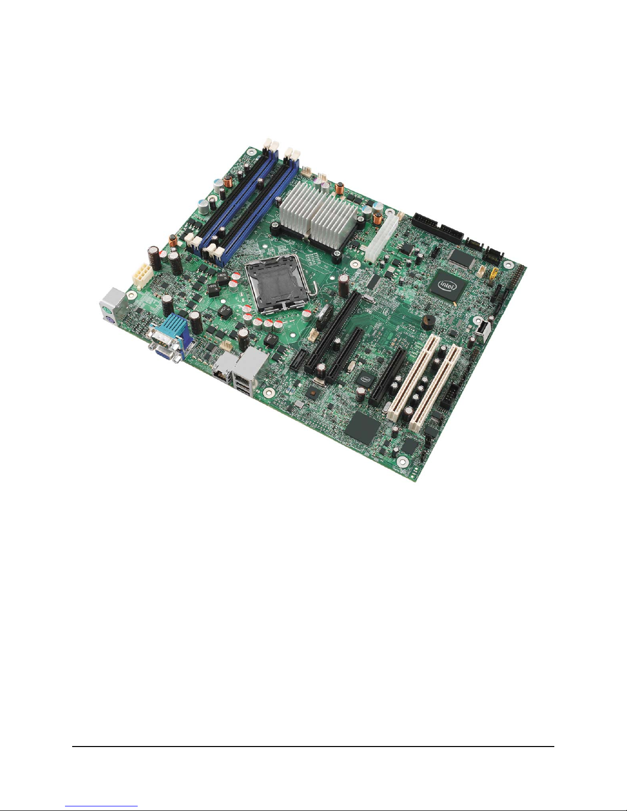
2.2 Server Board Layout
Figure 4. Intel® Server Board S3210SHLC
10 Revision 1.8
Intel Order Number: E14960-009
Page 23
Intel® Server Boards S3200SH/S3210SH TPS Server Board Overview
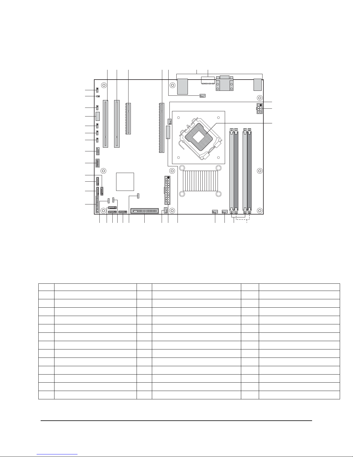
2.2.1 Server Board Mechanical Drawings
Figure 5. Intel® Server Board S3210SHLX – Hole and Component Positions
Revision 1.8 11
Intel Order Number: E14960-009
Page 24
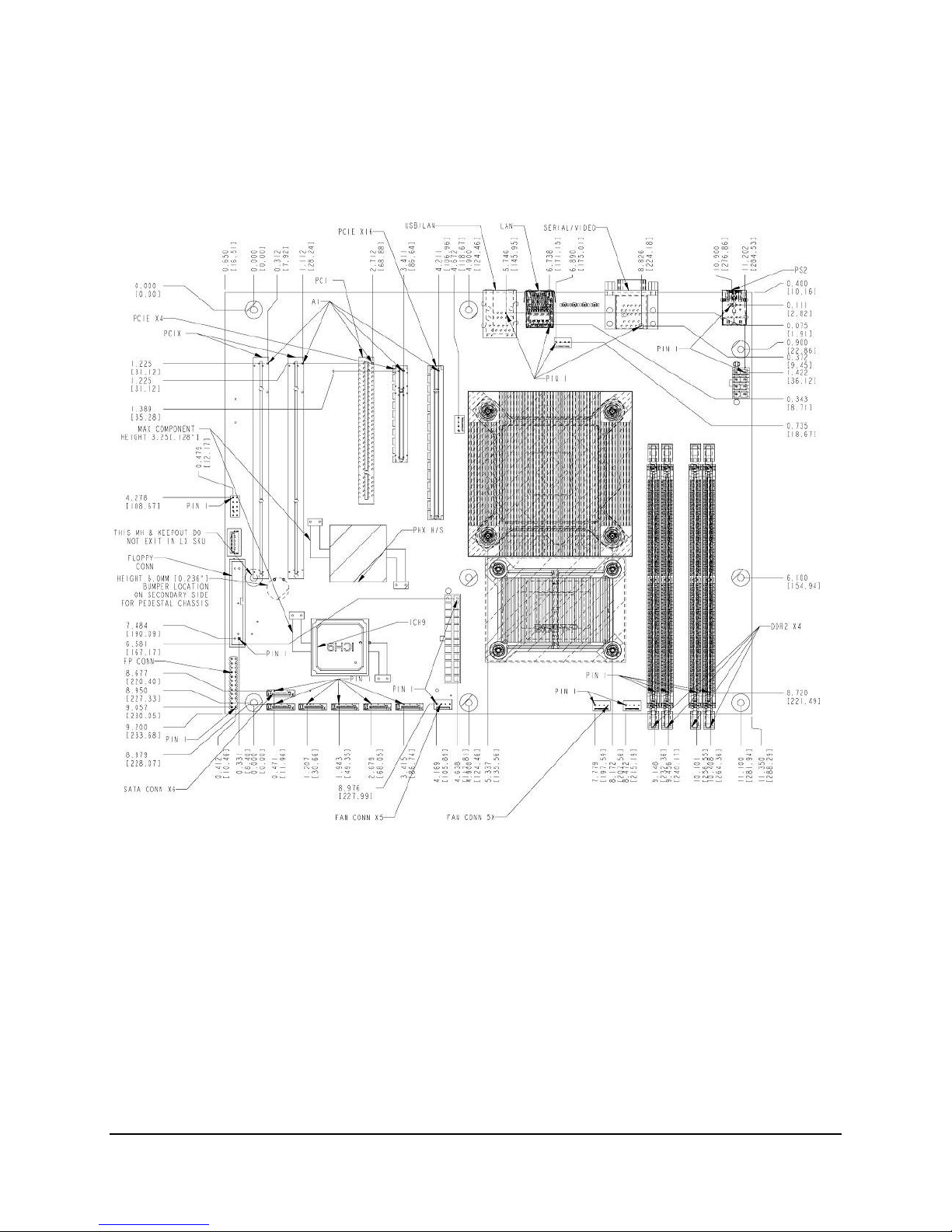
Server Board Overview Intel® Server Boards S3200SH/S3210SH TPS
Figure 6. Intel® Server Boards S3210SHLC/S3200SHL/S3200SHV – Hole and Component Positions
12 Revision 1.8
Intel Order Number: E14960-009
Page 25
Intel® Server Boards S3200SH/S3210SH TPS Functional Architecture
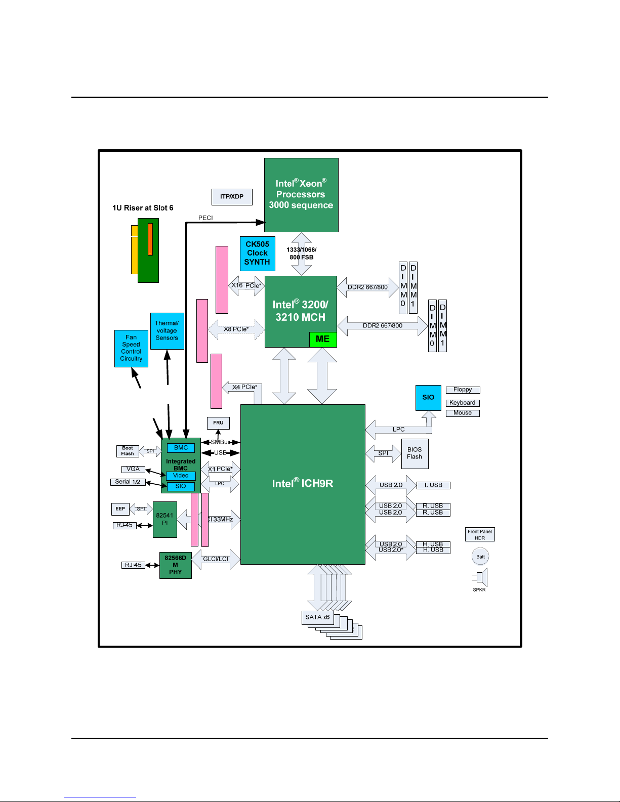
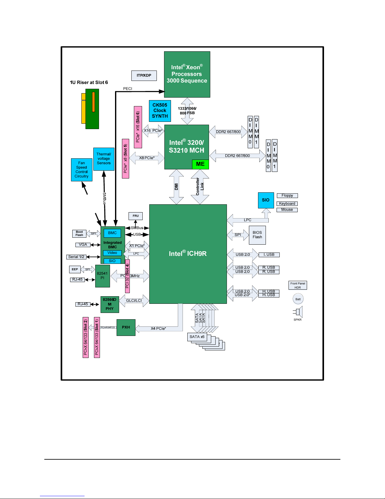
3. Functional Architecture
This chapter provides a high-level description of the functionality associated with the
architectural blocks that make up the Intel
PCIe* x16 (Slot 6)
PCIe* x8 (Slot 5)
S
MB
P
W
M
u
s
/
T
A
CH
PCI-E x8 (Slot 4)
®
Server Boards S3200SH/S3210SH.
DMI
Link
Controller
PCI 32 (Slot 1)
PCI 32 (Slot 2)
Figure 7. Intel® Server Boards S3200SH/S3210SH LC/L/V SKU–Block Diagram
Revision 1.8 13
SATA
SATA
SATA
Intel Order Number: E14960-009
Page 26
Functional Architecture Intel® Server Boards S3200SH/S3210SH TPS
P
W
M
/
T
A
CH
Figure 8. Intel® Server Systems S3200SH/S3210SH LX SKU–Block Diagram
14 Revision 1.8
Intel Order Number: E14960-009
Page 27

Intel® Server Boards S3200SH/S3210SH TPS Functional Architecture
3.1 Processor Sub-System
The server board supports the following processors:
Intel
Intel
Intel
Intel
®
Xeon® processor 3000 series
®
Xeon® processor 3100 series
®
Xeon® processor 3200 series
®
Xeon® processor 3300 series
The server board does not support the following processors:
All Intel
All Intel
®
5XX and 6XX series processors
®
8XX and 9XX series processors
The processors built on 65 nm (nanometer) and 45 nm process technology in the 775-land
package use Flip-Chip Land Grid Array (FC-LGA4) package technology, and plug into a 775land LGA socket, referred to as the Intel
®
LGA775 socket.
The processors in the 775-land package are based on the same core micro-architecture. They
maintain compatibility with 32-bit software written for the IA-32 instruction set, while supporting
64-bit native mode operation when coupled with supported 64-bit operating systems and
applications.
3.1.1 Processor Voltage Regulator Down (VRD)
The server board has a VRD (Voltage Regulator Down) to support one processor. It is compliant
with the VRD 12 DC-DC Converter Design Guide Line and provides a maximum of 125 A.
The board hardware monitors the processor VTTEN (Output enable for VTT) pin before turning
on the VRD. If the VTTEN pin of the processors is not asserted, the Power ON Logic will not
turn on the VRD.
3.1.2 Reset Configuration Logic
The BIOS determines the processor stepping and processor cache size through the CPUID
instruction. The processor information is read at every system power-on.
Note: The processor speed is the processor power-on reset default value. No manual processor
speed setting options exist either in the form of a BIOS setup option or jumpers.
Revision 1.8 15
Intel Order Number: E14960-009
Page 28
Functional Architecture Intel® Server Boards S3200SH/S3210SH TPS
Table 3. Processor Support Matrix
Process Name Socket Core Frequency Cache size FSB Frequency
Intel® Xeon® processor
3000 series
Intel® Xeon® processor
3100 series
Intel® Xeon® processor
3200 series
Intel® Xeon® processor
3300 series
®
LGA775
Intel
®
LGA775 TBD TBD 1333 MHZ
Intel
®
LGA775
Intel
®
LGA775 TBD TBD 1333 MHZ
Intel
1.86 GHz –
2.66 GHz
2.13 GHz –
2.40 GHz
2 MB or 4 MB 1066 MHz
8 MB 1066 MHz
®
3.2 Intel
The server board is designed around the Intel® 3200/3210 Chipset. The chipset provides an
integrated I/O bridge and memory controller, and a flexible I/O subsystem core (PCI Express*).
The chipset consists of three primary components.
3.2.1
The Intel
The role of the MCH in the system is to manage the flow of information between its four
interfaces:
Processor Interface (FSB)
System Memory Interface (DDR2)
DMI interface to the Intel
PCI Express* connectivity to one or two PCI Express* x8 connectors
The feature list of the MCH includes:
Processor / Host Interface
System Memory Controller
DMI Interface
3200/3210 Chipset
Intel® 3200/3210 Chipset MCH: Memory Control Hub
®
3200/3210 Chipset is designed for use with Intel® processors in a UP server platform.
®
ICH9R South Bridge
o Supports LGA775 processors in an UP System configuration
o 200/266/333 MHz FSB Clock frequency
o GTL+ bus drivers with integrated GTL termination resistors
o Supports 512 Mbit and 1 Gbit memory technologies
o DDR2 – 667, 800 MHz
o 8 GB addressable memory
o Supports unbuffered, ECC and non-ECC DIMMs
o No support for DIMMs less than 512 MB and memory speeds less than 667 MHz
16 Revision 1.8
Intel Order Number: E14960-009
Page 29

Intel® Server Boards S3200SH/S3210SH TPS Functional Architecture
o Interface to ICH9R South Bridge
o 100 MHz reference clock shared with PCI Express* interface(s)
PCI Express* x8 Interface
o Connected to two PCI Express* X8 connectors as shown in the block diagram
o Compliant with the PCI Express* base specification
The MCH accepts access requests from the host (processor) bus and directs those accesses to
memory or to one of the PCI Express* or PCI buses. The MCH monitors the host bus,
examining addresses for each request. Accesses may be directed to the following queues:
A memory request queue for subsequent forwarding to the memory subsystem
An outbound request queue for subsequent forwarding to one of the PCI Express* or
PCI buses
The MCH also accepts inbound requests from the Intel
®
ICH9R. The MCH is responsible for
generating the appropriate controls to control data transfer to and from memory.
The MCH is a FC-BGA device and uses the proven components of the following previous
generations:
Hub interface unit
PCI Express* interface unit
DDR2 memory interface unit
The MCH incorporates an integrated PCI Express* interface. The PCI Express* interface allows
the MCH to directly interface with the PCI Express* devices. The MCH also increases the main
memory interface bandwidth and maximum memory configuration with a 72-bit wide memory
interface.
The MCH integrates the following main functions:
An integrated high performance main memory subsystem
A PCI Express* bus which provides an interface to the PCI Express* devices (Fully
compliant to the PCI Express* Base Specification, Rev 1.0a)
A DMI which provides an interface to the Intel
®
ICH9R
Other features provided by the MCH include the following:
Full support of ECC on the processor bus
Twelve deep in-order queue, two deep defer queue
Full support of unbuffered DDR2 ECC DIMMs
Support for 512 MB, 1 GB, and 2 GB DDR2 memory modules
3.2.1.1 Segment F PCI Express* x8
The MCH PCI Express* Lanes 0~7 provide an x8 PCI Express* connection directly to the MCH.
This resource can support x1, x4, and x 8 PCI Express* add-in cards or cards through the I/O
riser when using the riser slot for the L board SKU.
Revision 1.8 17
Table 4. Segment F Connections
Intel Order Number: E14960-009
Page 30
Functional Architecture Intel® Server Boards S3200SH/S3210SH TPS
Lane Device
Lane 0~7 Slot 6 (PCI Express* x16 with 8 Lanes layout)
3.2.1.2 MCH Memory Sub-System Overview
The MCH supports a 72-bit wide memory sub-system that can support a maximum of 8 GB of
DDR2 memory using 2 GB DIMMs. This configuration needs external registers for buffering the
memory address and control signals. The four chip selects are registered inside the MCH and
need no external registers for chip selects.
The memory interface runs at 667/800 MT/s. The memory interface supports a 72-bit wide
memory array. It uses seventeen address lines (BA [2:0] and MA [13:0]) and supports 512 MB,
1 GB, and 2 GB DRAM densities. The DDR DIMM interface supports single-bit error correction,
and multiple bit error detection.
3.2.1.3 DDR2 Configurations
The DDR2 interface supports up to 8 GB of main memory and supports single- and doubledensity DIMMs. The DDR2 can be any industry-standard DDR2. The following table shows the
DDR2 DIMM technology supported.
Table 5. Supported DDR2 Modules
DDR2-667/800 Un-buffered
SDRAM Module Matrix
DIMM
Capacity
512 MB 64M x 72 256 Mbit 32M x 8 18 / 2 / 4 13 / 2 / 10
512 MB 64M x 72 512 Mbit 64M x 8 9 / 1 / 4 14 / 2 / 10
1 GB 128M x 72 512 Mbit 64M x 8 18 / 2 / 4 14 / 2 / 10
1 GB 128M x 72 1 Gbit 128M x 8 9 / 1 / 8 14 / 4 / 10
2 GB 256M x 72 2 GB 128M x 8 18 / 2 / 8 14 / 8 / 10
DIMM Organization
SDRAM
Density
SDRAM
Organization
# SDRAM
Devices/rows/Banks
# Address bits
rows/Banks/column
3.2.1.4 Memory Population Rules and Configurations
You must follow a few rules when populating memory. The server board supports two DDR2
DIMM slots for channel A and two DDR2 DIMM slots for channel B. They are placed in a row
and numbered from 0 to 3 with DIMM0 being closest to the MCH. The four slots are partitioned
with channel A representing the channel A DIMMs (DIMM0 and DIMM1) and channel B
representing the channel B DIMMs (DIMM2 and DIMM3).
Note the following memory population rules:
If dual-channel operation is needed, you must populate channel A and channel B
identically (for example, same capacity).
Use DDR2 667/800 MHz memory only.
The slowest DIMM in the system determines the speed used on all the channels.
18 Revision 1.8
Intel Order Number: E14960-009
Page 31

Intel® Server Boards S3200SH/S3210SH TPS Functional Architecture
Supports ECC or non-ECC DIMMs.
Different memory technologies (size and density) can be used.
Single Channel Mode (either channel can be used): DIMM slots (within the same
channel) may be populated in any order.
Dual Channel Interleaved Mode: DIMM slots can be populated in any order as long as
the total memory in each channel is the same.
Dual Channel Asymmetric Mode: DIMM slots may be populated in any order.
3.2.2 PCI-X Hub (LX board SKU only)
The PCI-X Hub (PXH-V) is a peripheral chip that performs PCI/PCI-X bridging functions
between the PCI Express* interface and the PCI/PCI-X bus. The PXH-V contains two PCI bus
interfaces that can be independently configured to operate in PCI (33 or 66 MHz) or PCI-X
mode (66,100, or 133 MHz), for either 32 or 64 bits.
3.2.2.1 Segment E 64bit/133MHz PCI-X Subsystem
One 64-bit PCI-X
bus segment is directed through the PXH-V. This PCI-X segment (segment E)
provides the following:
o Two 3.3 V 64-bit PCI-X slots
On Segment E, PCI-X is capable of speeds up to 133 MHz operation and supports full-length
PCI and PCI-X adapters.
3.2.2.1.1 Device IDs (IDSEL)
Each device under the PCI-X
hub bridge has an IDSEL signal connected to one bit of AD
[31:16], which acts as a chip select on the PCI-X bus segment in configuration cycles. This
determines a unique PCI-X device ID value for use in configuration cycles. The following table
shows the bit to which each IDSEL signal is attached for P64-C devices and a corresponding
device description.
Table 6. Segment E Configuration IDs
IDSEL Value Device
18 PCI-X Slot 1 (64-bit/66-133 MHz) (LX board SKU only)
17 PCI-X Slot 2 (64-bit/66-133 MHz) (LX board SKU only)
3.2.2.1.2 Segment E Arbitration
The PX
H-V supports two PCI masters: two PCI-X slots or one riser slot. All PCI masters must
arbitrate for PCI access using resources supplied by the PXH-V. The host bridge PCI interface
(PXH-V) arbitration lines REQx* and GNTx* are a special case because they are internal to the
host bridge. Table 7 defines the arbitration connections.
Table 7. Segment D Arbitration Connections
Revision 1.8 19
Intel Order Number: E14960-009
Page 32

Functional Architecture Intel® Server Boards S3200SH/S3210SH TPS
Baseboard Signals Device
PCIX REQ_N1/GNT_N1 PCI-X Slot 1 (64-bit/66-133 MHz) (LX board SKU only)
PCIX REQ_N0/GNT_N0 PCI-X Slot 2 (64-bit/66-133 MHz) ( LX board SKU only)
3.2.3 Intel
®
ICH9R: I/O Controller Hub 9R
3.2.3.1 Direct Media Interface (DMI)
DMI is the name given to the chip-to-chip connection between the Memory Controller Hub and
the Intel
Deviations of the DMI from standard PCI Express* specifications are described in the Intel
®
ICH9. DMI is a x4 link that mostly adheres to the PCI Express* specification.
®
ICH9 CSPEC.
3.2.3.2 Controller Link (M-Link)
Controller Link is the name given to the interconnect that connects the north bridge (MCH) to
the LAN Controller in the Intel
®
ICH9. The Management Engine (ME) resides in the MCH and
communicates with the ICH9 LAN Controller over this interface.
3.2.3.3 PCI Express* Interfaces
The ICH9R provides six PCI Express* root ports (GEN1) which are compliant with the PCI
Express* Base Specification, Revision 1.1. You can statically configure the PCI Express* root
ports 1-4 as four x 1 ports, or ganged together to form two x 2 ports, one x 2 with two x1 ports,
or one x4 port. Ports 5 and 6 can only be used as two x1 ports or one x2. The x4 configuration
supports lane reversal. Each Root Port fully supports 2.5 Gb/s bandwidth in each direction.
The root ports 1-4 are combined to form a single x4 link connecting to a PCI Express* x8
connector. Port 5 and 6 are used to support the dual GBe LAN channels.
3.2.3.4 Serial ATA II Interface
The Intel
®
ICH9 has an integrated SATA II host controller that supports independent DMA
operation on the six Ports and supports data transfer rates of up to 300 MB/Sec. The SATA II
controller provides two modes of operation – a legacy mode using I/O space and an Advanced
Host Controller Interface (AHCI) mode using memory space.
3.2.3.5 PCI Interface
The Intel
®
ICH9 PCI interface provides a 33 MHz, 3.3 V, Revision 2.3 implementation. Except
for PME#, all PCI signals are 5 V tolerant. The ICH9 integrates a PCI arbiter that supports up to
seven external PCI bus masters in addition to the internal ICH9 requests. This allows for
combinations of up to four PCI down devices and/or PCI slots.
The server board supports one NIC, the 82541PI Gigabit Ethernet controller, and two PCI slots.
3.2.3.6 Low Pin Count Interface (LPC)
The Low Pin Count interface on the Intel
®
ICH9 provides a low system cost design interface
solution for connecting the Super I/O for the legacy interfaces such as the parallel port, serial
port, floppy drive, and so on.
20 Revision 1.8
Intel Order Number: E14960-009
Page 33

Intel® Server Boards S3200SH/S3210SH TPS Functional Architecture
3.2.3.7 Compatibility Modules
®
The Intel
ICH9 incorporates various compatibility modules such as DMA controller,
timer/counters, and interrupt controller. The DMA controller incorporates the logic of two 8237
DMA controllers with seven independently programmable channels. Channels 0 to 3 are
hardwired to 8-bit, count-by-byte transfers and channels 5 to 7 are hardwired to 16-bit, count-byword transfers. DMA channel 4 is used to cascade the two 8327 controllers together. The DMA
controller is used to support the LPC DMA.
The LPC DMA is handled through the LDRQ# lines from peripherals and special encoding on
LAD[3:0] from the host.
The timer/counter block contains three counters equivalent in function to those found in one
8254 programmable internal timer. These three counters are combined to provide the system
timer function and speaker tone. The 14.318 MHz oscillator input provides the clock source for
these three counters.
The Intel
®
ICH9 provides an ISA compatible Programmable Interrupt Controller (PIC) that
incorporates the functionality of two 8259 interrupt controllers. Each 8259 supports eight
interrupts that are cascaded with one master controller interrupt 2 for fifteen programmable
interrupts. The interrupts are system timer, keyboard controller, serial ports, parallel ports,
floppy disk, mouse, DMA channels, and mapped PCI-based interrupts.
3.2.3.8 Universal Serial Bus (USB) Controller
The Intel
USB 2.0 ports. All twelve ports are high-speed, full-speed, and low-speed capable. The port
routing logic of the Intel
controllers or by the EHCI controller. The Intel
®
ICH9 contains two EHCI and six UHCI USB controllers providing support for twelve
®
ICH9 determines whether a USB port is controlled by one of the UHCI
®
ICH9 also implements a USB 2.0 based debug
port.
3.2.3.9 Real Time Clock (RTC)
The Intel
®
ICH9 contains a Motorola MS146818A* functionally compatible Real-Time Clock
(RTC) with two 128-Byte banks of battery backed RAM. The RTC performs two key functions on
the server board:
Keeping track of the time of day
Storing system configuration data even when the system is powered down.
The RTC operates on a 32.768 KHz (Kilohertz) crystal and a 3 V lithium battery.
3.2.3.10 GPIO
The Intel
®
ICH9 contains 61 General Purpose Inputs and Outputs (GPIO) for custom system
design.
3.2.3.11 Enhanced Power Management
The Intel
®
ICH9 supports the Advanced Configuration and Power Interface, Version 2.0 (ACPI)
that provides power and thermal management. The ICH9 also supports the Manageability
Engine Power Management Support for new wake events from the MCH Management Engine.
Revision 1.8 21
Intel Order Number: E14960-009
Page 34

Functional Architecture Intel® Server Boards S3200SH/S3210SH TPS
The server board fully complies with the Advanced Configuration and Power Interface (ACPI)
specifications, Revision 2.0.
3.2.3.12 System Management Interface
The Intel
with SMBus slaves. This interface is compatible with most I
®
ICH9 functions as a SMBus host controller and allows the processor to communicate
2
C devices. The ICH9 also supports
slave functionality. The SMBus logic exists in device 31: function 3 configuration space.
3.2.3.13 Intel
®
The Intel
ICH9 integrates two thermal sensors that monitor the temperature within the die.
Those sensors support Intel
the management engine (ME) residing in the MCH and requires SPI flash to host the Intel
®
Quiet System Technology (Intel® QST)
®
Quiet System Technology (Intel® QST). Intel® QST is controlled by
®
QST
firmware.
The Intel
®
ICH9 integrates four fan speed TACH sensors and three fan speed controllers,
PWMs. Up to four system fans can be monitored and controlled. The ICH9 implements a single
wire Simple Serial Transport (SST) bus that allows connection of up to five SST thermal or
voltage monitoring devices. The ICH9 also supports the Platform Environmental Control
Interface (PECI) that provides access to the CPU thermal data.
The server board does not support ME or Intel
®
QST. The integrated BMC firmware controls the
fan speed.
3.2.3.14 Serial Peripheral Interface (SPI)
The Serial Peripheral Interface (SPI) is a 4-pin interface that provides a
alternative for the system flash versus the Firmware Hub on the LPC Bus. The Intel
potentially lower-cost
®
ICH9
supports two SPI flash components using two separate chip select pins. Each component can
be up to 16 MB in size and operate in SPI Fast Read Instructions at frequencies of 20 MHZ or
33 MHz.
The SPI Interface consists of the following components:
Clock (CLK)
Master Out Slave In (MOSI)
Master In Slave Out (MISO)
Chip Select (CS#)
The SPI uses a Master – Slave protocol for communication.
The SPI flash may operate in two operational modes: descriptor and non-descriptor. When
operating in non-descriptor mode, the SPI Flash can only support the BIOS through register
accesses.
When operating in descriptor mode, the ICH9 allows a single SPI flash device to store system
BIOS, Firmware, and Gigabit Ethernet EEPROM information.
22 Revision 1.8
Intel Order Number: E14960-009
Page 35

Intel® Server Boards S3200SH/S3210SH TPS Functional Architecture
When SPI is selected by the Boot BIOS Destination Strap and a SPI Device is detected by the
®
Intel
ICH9, LPC-based BIOS Flash is disabled. The boot destination strap is sampled by the
ICH9 at pins GNT# and SPI_CS1# on the rising edge of the PWROK input. Alternately, the
ICH9 supports soft straps when operating in Descriptor Mode. The ICH9 reads the soft strap
data out of the SPI device prior to de-assertion of reset to the Manageability Engine and the
Host system.
GNT# and SPI_CS1# are both pulled-up with soft resistors internal to the Intel
®
ICH9. The
default BIOS flash without external straps is the FWH. For manufacturing or debugging support,
the BIOS cycles may also be directed to the PCI bridge via the same external flash.
Configurations other than the default are selected using 2.2K pull-up or pull-down resistors.
The server board supports the boot BIOS Destination Selection as defined in Table 8.
Table 8. Boot BIOS Destination Selection
GNT# SPI_CS1# ROUTING
0 1 Flash Cycles Routed to SPI (Default)
1 0 Flash Cycles Routed to PCI (Test only)
1 1 Flash Cycles Routed to LPC (Test only)
The SPI flash meets the following requirements:
Erase size capability of 4 Kbyte or 64 Kbyte
SPI device meets the command set per Table 9
For streamlined software development, command and opcode C7h (for Full Chip Erase) is
recommended.
Supports JEDEC ID OP Code 9FH.
Supports multiple writes to a page without requiring a preceding command (minimum
512 writes).
Ignores the upper address bit. For example, an address of FFFFFFFFh simply aliases to
the top of the flash memory.
Supports SPI Compatibility Mode 0.
Receipt of an unsupported command causes a completed cycle without impact to the
flash content.
Minimum density of 16 Mb (BIOS + Gbe).
To disable write protection, power up in an unlocked state or use the write status
register.
Commands Opcode Notes
Write Status 01h
Revision 1.8 23
Table 9. SPI Required Command Codes
If the command is supported, the opcode
Intel Order Number: E14960-009
Page 36

Functional Architecture Intel® Server Boards S3200SH/S3210SH TPS
Commands Opcode Notes
must be 01h.
Program Data 02h Write Data / Program Data
Read Data 03h
Write Disable 04h
Read Status 05h
Write Enable 06h
Fast Read 0Bh
Enable Write
Status Register
Erase Programmable 256 B, 4 Kbyte, 8 Kbyte, or 64 Kbyte erase
JEDEC ID 9Fh
50 or 06h
If the command is supported, the opcode
must be 06h.
The JEDEC Standard Manufacturer and
Device ID read method is defined in
Standard JESD21-C, PRN03-NV1.
The SPI Flash Memory device is an Atmel AT26DF321*, 32-mbit, 2.7 to 3.6 V serial interface
FLASH memory, Intel part number D64145-001/D64145-002. The AT26DF321 supports the
block erase command opcodes 20H and D8H, providing, respectively, 4-Kbytes or 64-Kbytes
block erase sizes. It installs directly onto the server board without the use of sockets.
3.2.3.15 Manageability
The Intel
®
ICH9 integrates several functions designed to manage the system and lower the total
cost of ownership (TCO) of the system. These system management functions are designed to
report errors, diagnose the system, and help the system recover from lockups without the aid of
an external microcontroller.
The management engine includes the following features:
A TCO Timer used to detect system locks
A Process Present Indicator that can determine if the processor fetches the first
instruction after reset
ECC Error reporting from the host controller
A Function Disable option to prevent disabled functions from generating interrupts and
power management events
An Intruder Detect input for system cases
3.2.3.16 Unused Intel
The server board does not support the following interfaces in the Intel
®
ICH9 Interfaces on the Server Board
®
ICH9:
1. AC’97 2.3 Controller – ICH9 integrates an Audio Codec ’97 Component Specifications,
Version 2.3 controller that can be used to attach an Audio Codec (AC), a Modem Codec
(MC), an Audio/Modem Codec (AMC), or a combination of ACs and a single MC
2. Intel
®
High Definition Audio
3. The Management Engine (ME), SST, Fan tachometer and PWM, and PEC controller
24 Revision 1.8
Intel Order Number: E14960-009
Page 37

Intel® Server Boards S3200SH/S3210SH TPS Functional Architecture
3.2.3.17 PCI Express* x4 Sub-system
®
The Intel
ICH9R supports one PCI Express* x4-lane interface that can also be configured as a
single x1 or x4-lane port. The PCI Express* interface allows direct connection with the PXH-V or
dedicated PCI Express* devices. (Fully compliant with the PCI Express* Base Specification,
Rev 1.0a).
3.2.3.18 PCI
One 32-bit PCI bus segment is directed through the Intel
A. This PCI Segment A supports two PCI connectors and one embedded Intel
®
ICH9R Interface defined as segment
®
82541PI LAN
controller.
The Intel
®
ICH9R does not contain a PATA device controller in the chipset; therefore, SATA
interface CD-ROM/DVD-ROMs are recommended for use with the server board.
3.2.3.19 SATA Controller
The Intel
®
ICH9R contains six SATA ports that support data transfer rates up to 300 Mbyte/s per
port.
3.2.3.20 Compatibility Modules (DMA Controller, Timer/Counters, Interrupt Controller)
The Intel
®
ICH9R provides the functionality of two-cascaded 82C59 with the capability to handle
15 interrupts. It also supports processor system bus interrupts.
3.2.3.21 Advanced Programmable Interrupt Controller (APIC)
The APICs in the Intel
®
ICH9R use messages on the FSB for interrupt generation and
notification to the processor.
3.2.3.22 Universal Serial Bus (USB) Controller
The Intel
®
ICH9R contains one EHCI USB 2.0 controller and can support four USB ports. The
USB controller moves data between main memory and up to four USB connectors. All ports
function identically and with the same bandwidth.
The server board provides two external USB ports on the rear panel of the server board. The
dual-stack USB connector is located within the standard ATX I/O panel area. The Universal
Serial Bus Specification, Revision 1.1 defines the external connectors.
The third/fourth USB port is optional and can be accessed by cabling from an internal 9-pin
connector located on the server board to an external USB port located either in front or the rear
of a chassis.
3.2.3.23 Enhanced Power Management
One of the embedded features of the Intel
implements ACPI-compliant power management features. The server board supports sleep
states S1, S4, and S5.
Revision 1.8 25
®
ICH9R is a power management controller. It
Intel Order Number: E14960-009
Page 38

Functional Architecture Intel® Server Boards S3200SH/S3210SH TPS
3.3 Memory Sub-System
The server board supports up to four DIMM slots for a maximum memory capacity of 8 GB. The
DIMM organization is x72, which includes eight ECC check bits. The memory interface runs at
533/667 MTs. The memory controller supports the following:
Single-bit error correction
Multiple-bit error detection
Memory using 512 Mbit, 1 Gbit, or 2 Gbit DRAM based on memory technology
Memory can be implemented with either single-sided (one row) or double-sided (two rows)
DIMMs.
3.3.1 Memory Configuration
The memory interface between the MCH and the DIMMs is a 72-bit (ECC) wide interface.
There are two banks of DIMMs, labeled 1 and 2. Bank 1 contains DIMM socket locations
DIMM_1A and DIMM_2A. Bank 2 contains DIMM socket locations DIMM_1B and DIMM_2B.
The sockets associated with each bank or “channel,” are located next to each other and the
DIMM socket identifiers are marked on the server board silkscreen near the DIMM socket. Bank
1 is associated with Memory Channel A while Bank 2 is associated with Memory Channel B.
When only two DIMM modules are used, the population order must be DIMM_1A, DIMM_1B to
ensure dual channel operating mode. For more information, see Figure 9.
In order to operate in dual channel dynamic paging mode, the following conditions must be met:
Two identical DIMMs are installed, one each in DIMM_1A and DIMM_1B
Four identical DIMMs are installed (one in each socket location)
Note: Three DIMMs cannot be installed on the server board. This configuration is not
supported. DIMMs that are not “matched” (same type and speed) are not supported. Identical
memory parts are preferred.
The system is designed to populate any rank on either channel including either degenerate
single channel case.
DIMM and memory configurations must adhere to the following:
DDR2 667/800 MHz, unbuffered, DDR2 DIMM modules
DIMM organization: x64 non-ECC or x72 ECC
Pin count: 240
DIMM capacity: 512 MB, 1 GB, and 2 GB DIMMs
Serial PD: JEDEC Rev 2.0
Voltage options: 1.8 V
Interface: SSTL2
26 Revision 1.8
Intel Order Number: E14960-009
Page 39

Intel® Server Boards S3200SH/S3210SH TPS Functional Architecture
Table 10. Memory Bank Labels and DIMM Population Order
Location DIMM Label Channel Population Order
J8J1 (DIMM_1A) A 1
J8J2 (DIMM_2A) A 3
J9J1 (DIMM_1B) B 2
J9J2 (DIMM_2B) B 4
Revision 1.8 27
Figure 9. Memory Bank Label Definition
Intel Order Number: E14960-009
Page 40

Functional Architecture Intel® Server Boards S3200SH/S3210SH TPS
Table 11. Characteristics of Dual/Single Channel Configuration with or without Dynamic Mode
Throughput Level Configuration Characteristics
Highest Dual channel with dynamic paging mode All DIMMs matched
Dual channel without dynamic paging mode DIMMs matched from Channel A to Channel B
Single channel with dynamic paging mode Single DIMM or DIMMs matched within a
Lowest Single channel without dynamic paging
mode
DIMMs not matched within channels
channel
DIMMs not matched
3.3.2 Memory DIMM Support
The board supports unbuffered (not registered) DDR2 667/800 ECC or non-ECC DIMMs
operating at 667/800 MT/s.
Note: Only DIMMs tested and qualified by Intel or a designated memory test vendor are
supported on this board. All DIMMs are supported by design, but only fully qualified DIMMs are
supported on the board.
The minimum supported DIMM size is 512 MB. Therefore, the minimum main memory
configuration is 1 x 512 MB or 512 MB. The largest size DIMM supported is 2 GB and as such,
the maximum main memory configuration is 8 GB implemented by 4 x 2 GB DIMMs.
Unbuffered DDR2 667/800 compliant, ECC x8 and Non-ECC x8 or x16 memory DIMMs
are supported.
ECC single-bit errors (SBE) can be detected and corrected. Multiple-bit errors (MBE)
can only be detected.
The maximum memory capacity is 8 GB via four 2 GB DIMM modules.
The minimum memory capacity is 512 MB via a single 512 MB DIMM module.
3.4 I/O Sub-System
3.4.1 PCI Subsystem
The primary I/O buses for the server board are five independent PCI bus segments providing
PCI, PCI Express*, and PCI-X resources (LX board SKU only). The PCI buses comply with the
PCI Local Bus Specification, Rev 2.3.
PCI segments A, B, C, and D are directed through the Intel
independently configured to PXH-V which is through the Intel
interface. PCI Segment F is directed through the MCH by PCI Express* x8 interface. Table 12
lists the characteristics of the three PCI bus segments.
®
ICH9R. PCI segment E is
®
ICH9R by PCI Express* x4
28 Revision 1.8
Intel Order Number: E14960-009
Page 41

Intel® Server Boards S3200SH/S3210SH TPS Functional Architecture
Table 12. PCI Bus Segment Characteristics
PCI Bus
Segment
A 3.3V 32 bits 33 MHz PCI 32 Slot 1, Slot 2, NIC 2, video
B 3.3V 1 lane 2.5 GHz x1 PCI Express* Slot 3, X4 physical connector
C 3.3V 1 lane 2.5 GHz x1 PCI Express* NIC 1
D 3.3V 4 lane 2.5 GHz x4 PCI Express* Slot 4, PXH, X8 physical connector
E 3.3V 64 bits 66/100/133 MHz PCI-64 Slot 5, Slot 6 through riser card
F 3.3V 8 lanes 2.5 GHz x8 PCI Express* Slot 6, X8 physical connector
Voltage Width Speed Type PCI I/O Card Slots
3.4.1.1 P32-A: 32-bit, 33-MHz PCI Sub-system
The Intel
®
ICH9R provides a Legacy 32-bit PCI sub-system and acts as the central resource on
this PCI interface. P32-A supports the following embedded devices and connectors:
One Intel
®
82541PI Fast Ethernet Controller
Two slots capable of supporting full length PCI add-in cards operating at 33 MHz
3.4.1.1.1 Device IDs (IDSEL)
Each device under the PCI hub bridge has its IDSEL signal connected to one bit of AD (31:16),
which acts as a chip select on the PCI bus segment in configuration cycles. This determines a
unique PCI device ID value for use in configuration cycles. The following table shows the bit to
which each IDSEL signal is attached for segment A devices and the corresponding device
description.
Table 13. Segment A Configuration IDs
IDSEL Value Device
21 Intel® 82541PI LAN (NIC2)
17 PCI Slot 1(32b/33MHz)
16 PCI slot 2(32b/33MHz)
3.4.1.1.2 Segment A Arbitration
PCI segment A supports two PCI devices: the Intel
PCI masters must arbitrate for PCI access using resources supplied by the Intel
®
ICH9R and one PCI bus master (NIC). All
®
ICH9R. The
host bridge PCI interface (ICH9R) arbitration lines REQx* and GNTx* are a special case in that
they are internal to the host bridge. Table 14 defines the arbitration connections.
Revision 1.8 29
Intel Order Number: E14960-009
Page 42

Functional Architecture Intel® Server Boards S3200SH/S3210SH TPS
Table 14. Segment A Arbitration Connections
Baseboard Signals Device
PCI REQ_N5/GNT_N5 Intel® 82541PI LAN (NIC2)
PCI REQ_N1/GNT_N1 PCI Slot 1 (32-bit/33 MHz)
PCI REQ_N0/GNT_N0 PCI Slot 2 (32-bit/33 MHz)
3.4.1.2 PCI Interface for Video subsystem
The server board graphics subsystem is connected to the Intel
®
ICH9R with a PCI Express* x1
bus.
3.4.2 Interrupt Routing
The board interrupt architecture accommodates both PC-compatible PIC mode and APIC mode
interrupts through the use of integrated I/O APICs in the Intel
3.4.2.1 Legacy Interrupt Routing
For PC-compatible mode, the Intel
®
ICH9R provides two 82C59-compatible interrupt controllers.
The two controllers are cascaded with interrupt levels 8 through 15 entering on level 2 of the
primary interrupt controller (standard PC configuration). A single interrupt signal is presented to
the processor, to which the processor responds for servicing. The Intel
configuration registers that define which interrupt source logically maps to I/O APIC INTx pins.
®
ICH9R.
®
ICH9R contains
The Intel
APIC bus. The numbers in Table 15 indicate the Intel
®
ICH9R handles both PCI and IRQ interrupts. The Intel
®
ICH9R PCI interrupt input pin to which
the associated device interrupt (INTA, INTB, INTC, INTD, INTE, INTF, INTG, INTH for PCI bus
and PXIRQ0, PXIRQ1, PXIRQ2, PXIRQ3 for PCI-X bus) is connected. The Intel
®
ICH9R translates these to the
®
ICH9R I/O
APIC exists on the I/O APIC bus with the processor.
Table 15. PCI AND PCI-X Interrupt Routing/Sharing
Interrupt INT A INT B INT C INT D
Intel® 82541PI LAN (NIC2) PIRQB
Integrated BMC PIRQC
PCI Slot 1 (PCI 32-bit/33 MHz) PIRQG PIRQF PIRQE PIRQH
PCI Slot 2 (PCI 32-bit/33 MHz) PIRQF PIRQG PIRQH PIRQE
PCI-X Slot 5 (64-bit/133 MHz) (LX board SKU
only)
PCI-X Slot 6 (64-bit/133 MHz) (Riser, LX board
SKU only)
PXIRQ5 PXIRQ6 PXIRQ7 PXIRQ4
PXIRQ0 PXIRQ1 PXIRQ2 PXIRQ3
30 Revision 1.8
Intel Order Number: E14960-009
Page 43

Intel® Server Boards S3200SH/S3210SH TPS Functional Architecture
3.4.2.2 APIC Interrupt Routing
®
For APIC mode, the server board interrupt architecture incorporates three Intel
devices to manage and broadcast interrupts to local APICs in each processor. The Intel
I/O APIC
®
I/O
APICs monitor each interrupt on each PCI device including PCI slots in addition to the ISA
compatibility interrupts IRQ (0-15).
When an interrupt occurs, a message corresponding to the interrupt is sent across a three-wire
serial interface to the local APICs. The APIC bus minimizes interrupt latency time for
compatibility interrupt sources. The I/O APICs can also supply greater than 16 interrupt levels to
the processor(s). This APIC bus consists of an APIC clock and two bi-directional data lines.
3.4.2.3 Legacy Interrupt Sources
Table 16 recommends the logical interrupt mapping of interrupt sources on the board. The
actual interrupt map is defined using configuration registers in the Intel
®
ICH9R.
Table 16. Interrupt Definitions
ISA Interrupt Description
INTR Processor interrupt.
NMI NMI to processor.
IRQ0 System timer
IRQ1 Keyboard interrupt.
IRQ2 Slave PIC
IRQ3 Serial port 1 interrupt from Super I/O* device, user-configurable.
IRQ4 Serial port 1 interrupt from Super I/O* device, user-configurable.
IRQ5
IRQ6 Floppy disk.
IRQ7 Generic
IRQ8_L Active low RTC interrupt.
IRQ9 SCI*
IRQ10 Generic
IRQ11 Generic
IRQ12 Mouse interrupt.
IRQ13 Floaty processor.
IRQ14 Compatibility IDE interrupt from primary channel IDE devices 0 and 1
IRQ15 Secondary IDE Cable
SMI* System Management Interrupt: General purpose indicator sourced by the Intel® ICH9R to the
processor
3.4.2.4 Serialized IRQ Support
The server board supports a serialized interrupt delivery mechanism. Serialized Interrupt
Requests (SERIRQ) consist of a start frame, a minimum of 17 IRQ / data channels, and a stop
frame. Any slave device in the quiet mode may initiate the start frame. While in the continuous
mode, the start frame is initiated by the host controller.
Revision 1.8 31
Intel Order Number: E14960-009
Page 44

Functional Architecture Intel® Server Boards S3200SH/S3210SH TPS
3.4.3 PCI Error Handling
The PCI bus defines two error pins, PERR# and SERR#, for reporting PCI parity errors and
system errors, respectively. In the case of PERR#, the PCI bus master has the option to retry
the offending transaction or report it using SERR#. SERR# reports all other PCI-related errors. If
enabled by the BIOS, SERR# is routed to NMI.
32 Revision 1.8
Intel Order Number: E14960-009
Page 45

Intel® Server Boards S3200SH/S3210SH TPS Functional Architecture
®
®
IRQ0
IRQ1
IRQ2
IRQ3
IRQ4
IRQ5
IRQ6
IRQ7
IRQ8
IRQ9
IRQ10
IRQ11
IRQ12
IRQ13
IRQ14
IRQ15
IRQ16
IRQ17
IRQ18
IRQ19
IRQ20
IRQ21
IRQ22
IRQ23
Intel
ICH9R
Intel® ICH9R IOAPIC 0
DMI INTERFACE
Intel
ICH9R
8259PIC
x8
x8 PCI Express*
Connector
MCH
INTR
CPU
Revision 1.8 33
Figure 10. Interrupt Routing Diagram
Intel Order Number: E14960-009
Page 46

Functional Architecture Intel® Server Boards S3200SH/S3210SH TPS
y
ppy
p
®
Q
A
A
A
Timer
Ke
board
Cascade
Serial Port2/ISA
Serial Port1/ISA
ISA
Flo
/ISA
ISA
RTC
SCI/ISA
ISA
ISA
Mouse/ISA
Co
rocessor Error
P IDE/ISA
Not Used
Super I/O
Serialized IRQ Interface
SERIR
SERIRQ
PCI Interface
Routing
Intel
ICH9R Interrupt
Intel® 82541PI NIC
N/
N/A
N/
Slot 1 and 2 INTC
Slot 1 and 2 INT
Slot 1 and 2 INTD
Figure 11. Intel® ICH9R Interrupt Routing Diagram
PIRQA#
PIRQB#
PIRQC#
PIRQD#
PIRQE#
PIRQF#
PIRQG#
PIRQH#
34 Revision 1.8
Intel Order Number: E14960-009
Page 47

Intel® Server Boards S3200SH/S3210SH TPS Functional Architecture
A
A
A
A
A
A
A
A
A
A
A
A
A
A
A
A
A
A
A
A
A
A
A
A
PCI-X slot 6 INTD#
PCI-X slot 6 INTA#
PCI-X slot 6 INTC#
PCI-X slot 6 INTB#
PCI-X slot 5 INTD#
PCI-X slot 5 INTA#
PCI-X slot 5 INTB#
PCI-X slot 5 INTC#
N/
N/
N/
N/
N/
N/
N/
N/
PCI-X
Interface
N/
N/
N/
N/
N/
N/
N/
N/
N/
N/
N/
N/
N/
N/
N/
N/
Figure 12. PXH-V Interrupt Routing Diagram
PCI-X
Interface
PXH-V
Revision 1.8 35
Intel Order Number: E14960-009
Page 48

Functional Architecture Intel® Server Boards S3200SH/S3210SH TPS
3.5 BMC Controller
The Integrated Baseboard Management Controller (Integrated BMC) is a highly integrated
single-chip solution, integrating several devices typically found on servers. The Integrated BMC
is mainly targeted at next generation servers and provides a highly-integrated server class
product.
The Integrated BMC contains the following integrated subsystems and features.
Server Class Super I/O* functionality includes
Keyboard style/BT interface for BMC support
Two Fully Functional Serial Ports, compatible with the 16C550
Serial IRQ Support
SMI/SCI/PME Support
ACPI Compliant
Up to 16 Shared GPIO ports
Programmable Wake-up Event Support
Plug and Play Register Set
Power Supply Control
Watchdog timer compliant with Microsoft SHDG
LPC to SPI bridge for system BIOS support
Real Time Clock (RTC) module with external RTC interface
Baseboard Management Controller
IPMI 2.0 Compliant
Integrated 250 MHz 32-bit ARM9 processor
Six I2C SMBus Modules with Master-Slave support
Two independent 10/100 Ethernet Controllers with RMII support
LPC Master interface for non-volatile code storage
SPI Flash interface
Three UART for ICMB support
DDR2 16-bit up to 667 MHz memory interface
16 Mailbox Registers for communication between the host and the BMC
Watchdog timer
Three General Purpose Timers
Dedicated Real Time Clock for BMC
Up to 16 direct and 64 Serial GPIO ports
Ability to maintain text and graphics controller history
12 10-bit Analog to Digital Converters
Three Diode Inputs for Temperature measurements
36 Revision 1.8
Intel Order Number: E14960-009
Page 49

Intel® Server Boards S3200SH/S3210SH TPS Functional Architecture
Eight Fan Tach Inputs
Four Pulse Width Modulators (PWM)
Chassis Intrusion Logic with battery backed general purpose register
LED support with programmable blink rate control
Programmable IO Port snooping, which can be used to snoop on Port 80h
Unique Chip ID for each part, burned at the time of production testing
Hardware 32-bit Random Number generator
JTAG Master interface
On-Chip Test Infrastructure for testing BMC firmware
Graphics Controller Subsystem
Integrated Matrix Graphics Core
2D Hardware Graphics Acceleration
DDR2 memory interface supports up to 128 Mbytes of memory
Supports all display resolutions up to 1600 x 1200 16 bpp @ 75 Hz
High speed Integrated 24-bit RAMDAC
Single lane PCI Express* host interface
Integrated BMC Block Diagram
Interrupt
Controller
ARM926EJ-S
16K D & I
Cache
RTC &
General Purpose
TImers (3)
BMC & KVMS Subsystem
UART (3) GPIO
LPC
Interface
To Host
LPC
Interface
LPC to SPI
Flash Bridge
BMC & KVMS Subsystem Graphics Subsystem
Fan Tach (12)
PWM (4)
UART
(3)
Watchdog
Timer
I2C
(6)
KCS
BT &
Mailboxes
ADC
Thermal
Ethernet
MAC with
RMII (2)
System
Wakeup
Control
Real Time Clock
Interface
(external RTC)
USB
to Host
USB 1.1
&
USB 2.0
Crypto
Accelerator
Code
Memory
LPC Master,
JTAG Master,
& SPI FLash
DDR-II
16-bit
Memory
Controller
Graphics
Controller
JTAG
Master
DDR-II
(up to
667MHz)
Video
Output
PCIe x1
Interface
Revision 1.8 37
Intel Order Number: E14960-009
Page 50

Functional Architecture Intel® Server Boards S3200SH/S3210SH TPS
3.6 PCI Express* to PCI-X Bridge 6702PXH (PXH-V) (LX Board SKU Only)
The Intel® 6702PXH 64-bit PCI Hub is a peripheral chip that performs PCI bridging functions
between the PCI Express* interface and the PCI bus. The Intel
®
6702PXH 64-bit PCI Hub
contains a single PCI bus interface that can be configured to operate in PCI (33 or 66 MHz) or
PCI-X Mode 1 (66, 100, or 133 MHz).
The Intel
®
6702PXH 64-bit PCI Hub further supports the new PCI Standard Hot-Plug Controller
and Subsystem Specification, Revision 1.0. Each PCI interface contains an I/OxAPIC with 24
interrupts and a standard hot plug controller.
3.7 Clock Generator
A CK505 compliant Clock Synthesizer chip solution generates most of the required clocks on
the Intel
outputs at various frequencies, timings, and drive levels using a single parallel resonance
14.31818 MHz (50 ppm or less) crystal.
The CK505 clock generator supplies host clocks (at 200 MHz, 266 MHz, and 333 MHz),
100 MHz clocks, 48 MHz clocks, 33 MHz clocks, and 14 MHz clocks.
The CK505 has twelve SRC outputs targeted for PCI Express* applications at 100 MHz.
The CK505 is the main clock source for the entire system.
®
Server Board S3200SH. The CK505 synthesizes and distributes a multitude of clock
The clock generator supports the following:
o Differential host clock pairs for processor, MCH and XDP
o Differential 100 MHz to ICH9 (DMI and SATA), MCH, XDP, and PCI Express*
slots
o 33 MHz clocks for ICH9, SIO, SM712, Port 80/81h and PCI32 slots
o Single ended 48 MHz clock for the Intel
®
CH9 USB Controller
o Single ended 14.318 MHz clocks shared between the ICH9 and SIO
o Debug jumpers to manually select FSB/host clock frequency
SMBus interface for spread spectrum support
Option to retain register contents in PWRDWN# state
3.8 Super I/O
There is a Winbond* PC8374L super I/O located on the Intel® ICH9 LPC bus. This device uses
the following features on the server board:
LPC rev 1.1
Floppy Disk Controller with a Digital Data Separator
KB and Mouse Controller (KBC)
ACPI 2.0b Compliant
Sensor Path* Interface
38 Revision 1.8
Intel Order Number: E14960-009
Page 51

Intel® Server Boards S3200SH/S3210SH TPS Functional Architecture
3.9 GigE Controller 82541PI
The Intel® 82541 Gigabit Ethernet Controller is a single, compact component with integrated
Gigabit Ethernet Media Access Controller (MAC) and Physical Layer (PHY) function. This
device interfaces with the ICH9 using PCI 32 bit/33MHz. The server board uses this device
along with the integrated ICH9 MAC and external 82566 PHY to provide two Gigabit Ethernet
Ports.
The device has the following features:
Uses PCI 32-bit/33 MHz PCI Interface
IEEE802.3x compliant flow control support
Integrated PHY for full 10/100/1000 Mbps full and half duplex operation
On-board Microcontroller
Wake-On LAN (WOL) Support
IPMI support for server management
3.10 GigE PHY
The Intel® 82566 Gigabit Ethernet physical layer transceiver (PHY) is a single port device that
supports the integrated ICH9 Media Access Controller (MAC) at 10 Mbps, 100 Mbps, or 1000
Mbps.
The PHY is interfaced to the ICH9 using a high-speed serial interface, the Gigabit LAN Connect
Interface (GLCI). This interface operates using two capacitively coupled differential pairs; one
transmit pair and one receive pair.
The PHY is also interfaced to the ICH9 using a lower frequency LAN Connect Interface (LCI).
The LCI interface operates using eight single ended signals, one clock, three transmit, three
receive, and one reset/sync.
The dual interface, GLCI/LCI allows the interfaces to be dynamically controlled based on the
link speed. In gigabit Ethernet mode, the GLCI is used to transmit and receive data and the LCI
is used for Management Data Input/Output (MDIO). For all other link speeds including no-link
and power-down, the GLCI is electrically idle. In sleeping states S3 – S5, the gigabit Ethernet
link is not supported.
3.11 On-Board Components
3.11.1 Video Support
The server board includes an integrated VGA graphics engine in Integrated BMC that supports
standard VGA drivers with analog display capabilities. The graphics subsystem has 8 MB
memory to support the onboard video controller. The baseboard provides a standard 15-pin
VGA connector at the rear of the system, in the standard ATX I/O opening area. The video
Revision 1.8 39
Intel Order Number: E14960-009
Page 52

Functional Architecture Intel® Server Boards S3200SH/S3210SH TPS
controller is disabled by default in BIOS Setup when an off-board video adapter is detected in
either the PCI Express* or PCI slots.
40 Revision 1.8
Intel Order Number: E14960-009
Page 53

Intel® Server Boards S3200SH/S3210SH TPS Functional Architecture
3.11.1.1 Video Modes
Table 17. Video Modes
2D Video Mode Support 2D Mode Refresh Rate (Hz)
8 bpp 16 bpp 24 bpp 32 bpp
640x480 60, 72, 75, 90, 100 Supported Supported Supported Supported
800x600 60, 70, 75, 90, 100 Supported Supported Supported Supported
1024x768 60, 72, 75, 90, 100 Supported Supported Supported Supported
1280x1024 43, 60 Supported Supported Supported Supported
1280x1024 70, 72 Supported – Supported Supported
1600x1200 60, 66 Supported Supported Supported Supported
1600x1200 76, 85 Supported Supported Supported –
3D Video Mode Support with Z Buffer Enabled 3D Mode Refresh Rate (Hz)
8 bpp 16 bpp 24 bpp 32 bpp
640x480 60,72,75,90,100 Supported Supported Supported Supported
800x600 60,70,75,90,100 Supported Supported Supported Supported
1024x768 60,72,75,90,100 Supported Supported Supported Supported
1280x1024 43,60,70,72 Supported Supported – –
1600x1200 60,66,76,85 Supported – – –
3D Video Mode Support with Z Buffer Disabled 3D Mode Refresh Rate (Hz)
8 bpp 16 bpp 24 bpp 32 bpp
640x480 60,72,75,90,100 Supported Supported Supported Supported
800x600 60,70,75,90,100 Supported Supported Supported Supported
1024x768 60,72,75,90,100 Supported Supported Supported Supported
1280x1024 43,60,70,72 Supported Supported Supported –
1600x1200 60,66,76,85 Supported Supported – –
Revision 1.8 41
Intel Order Number: E14960-009
Page 54

Functional Architecture Intel® Server Boards S3200SH/S3210SH TPS
3.12 Replacing the Back-Up Battery
The lithium battery on the server board powers the RTC for up to ten years in the absence of
power. When the battery starts to weaken, it loses voltage, and the server settings stored in
CMOS RAM in the RTC (for example, the date and time) may be wrong. For a list of approved
devices, contact your customer service representative or dealer.
WARNING
Danger of explosion if battery is incorrectly replaced. Replace only with the same or equivalent
type recommended by the equipment manufacturer. Discard used batteries according to
manufacturer’s instructions.
ADVARSEL!
Lithiumbatteri - Eksplosionsfare ved fejlagtig håndtering. Udskiftning må kun ske med batteri af
samme fabrikat og type. Levér det brugte batteri tilbage til leverandøren.
ADVARSEL
Lithiumbatteri - Eksplosjonsfare. Ved utskifting benyttes kun batteri som anbefalt av
apparatfabrikanten. Brukt batteri returneres apparatleverandøren.
VARNING
Explosionsfara vid felaktigt batteribyte. Använd samma batterityp eller en ekvivalent typ som
rekommenderas av apparattillverkaren. Kassera använt batteri enligt fabrikantens instruktion.
VAROITUS
Paristo voi räjähtää, jos se on virheellisesti asennettu. Vaihda paristo ainoastaan
laitevalmistajan suosittelemaan tyyppiin. Hävitä käytetty paristo valmistajan ohjeiden mukaisesti.
42 Revision 1.8
Intel Order Number: E14960-009
Page 55

System BIOS Intel® Server Boards S3200SH/S3210SH TPS
4. System BIOS
4.1 BIOS Identification String
The BIOS Identification string uniquely identifies the revision of the BIOS used on the server.
The string is formatted as follows:
BoardFamilyID.OEMID.MajorRev.MinorRev.BuildID.BuildDateTime
Where:
BoardFamilyID = String name for this board family
OEMID = Three-character OEM ID. “86B” is used for Intel server boards
MajorRev = Two decimal digits
MinorRev = Two decimal digits
BuildID = Four decimal digits
BuildDateTime = Build date and time in MMDDYYYYHHMM format:
MM = Two-digit month
DD = Two-digit day of month
YYYY = Four-digit year
HH = Two-digit hour using 24-hour clock
MM = Two-digit minute
®
For example, Intel
AM displays the following BIOS ID string in the POST diagnostic screen:
Server Board S3200SH BIOS Build 3, generated on Jan 21, 2006 at 11:59
S3200.86B.01.00.0003.012120061159
The BIOS version in the Setup Utility displays as:
S3200.86B.01.00.0003
The BIOS ID identifies the BIOS image. It is not used to designate either the board ID Snow Hill
or the BIOS phase (Alpha, Beta, and so forth). The board ID is available in the SMBIOS type 2
structure in which the phase of the BIOS can be determined by the release notes associated
with the image. The Board ID is also available via setup.
Support for INT15H, Function DA8Ch (Get BIOSID) was removed. The BIOS ID must be read
from the SMBIOS type 0 structure.
Revision 1.8 43
Intel Order Number: E14960-009
Page 56

Intel® Server Boards S3200SH/S3210SH TPS System BIOS
4.2 Logo / Diagnostic Window
The logo / diagnostic window may be in one of two forms, quiet boot mode and verbose mode.
In quiet boot mode, a logo splash screen displays. In verbose mode, a system summary and
diagnostic screen display. The default is to display the logo in quiet boot mode. If no logo is
present in the flash ROM, or if quiet boot mode is disabled in the system configuration, the
summary and diagnostic screen display.
The diagnostic screen consists of the following information
BIOS ID
Total memory detected (total size of all installed DIMMs)
Processor information (Intel branded string, speed, and number of physical processors
identified)
Types of input devices (keyboard, mouse, and so forth) detected if plugged in (PS/2
and/or USB)
4.3 BIOS Setup Utility
The BIOS setup utility is a text-based utility that allows the user to configure the system and
view current settings and environment information for the platform devices. The setup utility
controls the platform's built-in devices.
The BIOS setup interface consists of a number of pages or screens. Each page contains
information or links to other pages. The first page in Setup displays a list of general categories
as links. These links lead to pages containing specific category’s configuration.
The following sections describe the look and behavior for platform setup.
4.3.1 Operation
BIOS Setup has the following features:
Localization. The BIOS is only available in English.
BIOS Setup is functional via console redirection over various terminal emulation
standards. This may limit some functionality for compatibility (for example, usage of
colors or some keys or key sequences or support of pointing devices).
4.3.1.1 Setup Page Layout
The setup page layout is sectioned into functional areas. Each occupies a specific area of the
screen and has dedicated functionality. Table 18 lists and describes each functional area.
44 Revision 1.8
Intel Order Number: E14960-009
Page 57

System BIOS Intel® Server Boards S3200SH/S3210SH TPS
Table 18. BIOS Setup Page Layout
Functional Area Description
Title Bar The title bar is located at the top of the screen and displays the title of the form
(page) the user is currently viewing. It may also display navigational information.
Setup Item List The Setup Item List is a set of controllable and informational items. Each item in the
list occupies the left and center columns in the middle of the screen. The left
column, the "Setup Item", is the subject of the item. The middle column, the
"Option", contains an informational value or choices of the subject.
A Setup Item may also be a hyperlink used to navigate form sets (pages). When it is
a hyperlink, a Setup Item only occupies the “Setup Item” column.
Item Specific Help Area The Item Specific Help area is located on the right side of the screen and contains
help text for the highlighted Setup Item. Help information includes the meaning and
usage of the item, allowable values, effects of the options, and so forth.
Keyboard Command Bar The Keyboard Command Bar is located at the bottom right of the screen and
continuously displays help for keyboard special keys and navigation keys. The
keyboard command bar is context-sensitive—it displays keys relevant to current
page and mode.
Status Bar The Status Bar occupies the bottom line of the screen. This line displays the BIOS
ID
4.3.1.2 Entering BIOS Setup
You start the BIOS Setup by pressing <F2> during boot time when the OEM (Original
Equipment Manufacturer) or Intel logo displays.
When Quiet Boot is disabled, the message “press <F2> to enter setup” displays on the
diagnostics screen.
4.3.1.3 Keyboard Commands
The bottom right portion of the Setup screen provides a list of commands used to navigate
through the Setup utility. These commands are displayed at all times.
Each setup menu page contains a number of features. Except those used for informative
purposes, each feature is associated with a value field. This field contains user-selectable
parameters. Depending on the security option chosen and in effect by the password, a menu
feature’s value may or may not be changeable. If a value is non-changeable, the feature’s value
field is inaccessible. It displays as “grayed out.” Table 19 lists these options.
Revision 1.8 45
Intel Order Number: E14960-009
Page 58

Intel® Server Boards S3200SH/S3210SH TPS System BIOS
Table 19. BIOS Setup: Keyboard Command Bar
Key Option Description
<Enter> Execute
Command
<Esc> Exit The <Esc> key provides a mechanism for backing out of any field. This key undoes
<Tab> Select Field Use the <Tab> key to move between fields. For example, use <Tab> to move from
- Change Value Use the minus key on the keypad to change the value of the current item to the
+ Change Value Use the plus key on the keypad to change the value of the current menu item to the
<F9> Setup Defaults Pressing <F9> causes the following message to display:
<F10> Save and Exit Pressing <F10> causes the following message to display:
Select Item Use the up arrow to select the previous value in a pick list, or the previous option in
Select Item The down arrow is used to select the next value in a menu item’s option list, or a
Select Menu Use the left and right arrow keys to move between the major menu pages. The
The <Enter> key activates sub-menus when the selected feature is a sub-menu, or
displays a pick list if a selected option has a value field, or selects a sub-field for
multi-valued features like time and date. If a pick list is displayed, the <Enter> key
selects the currently highlighted item, undoes the pick list, and returns the focus to
the parent menu.
the pressing of the Enter key. When the <Esc> key is pressed while editing any
field or selecting features of a menu, the parent menu is re-entered.
When the <Esc> key is pressed in any sub-menu, the parent menu is re-entered.
When the <Esc> key is pressed in any major menu, the exit confirmation window
displays and the user is asked whether changes can be discarded. If “No” is
selected and the <Enter> key is pressed, or if the <Esc> key is pressed, the user is
returned to where he/she was before <Esc> was pressed, without affecting any
existing settings. If “Yes” is selected and the <Enter> key is pressed, setup is
exited and the BIOS returns to the main System Options Menu screen.
a menu item's option list. Activate the selected item by pressing the <Enter> key.
value field’s pick list. Activate the selected item by pressing the <Enter> key.
keys have no effect if a sub-menu or pick list displays.
hours to minutes in the time item in the main menu.
previous value. This key scrolls through the values in the associated pick list
without displaying the full list.
next value. This key scrolls through the values in the associated pick list without
displaying the full list. On 106-key Japanese keyboards, the plus key has a different
scan code than the plus key on the other keyboard, but will have the same effect.
Load Optimized defaults? (Y/N)
If the <Y> key is pressed, all Setup fields are set to their default values. If the <N>
key is pressed, or if the <Esc> key is pressed, the user is returned to where they
were before <F9> was pressed without affecting any existing field values
Save Configuration and Reset? (Y/N)
If the <Y> key is pressed, all changes are saved and Setup is exited. If the <N> key
is pressed, or the <Esc> key is pressed, the user is returned to where they were
before <F10> was pressed without affecting any existing values.
4.3.1.4 Menu Selection Bar
The Menu Selection Bar is located at the top of the screen. It displays the major menu
selections available to the user.
46 Revision 1.8
Intel Order Number: E14960-009
Page 59

System BIOS Intel® Server Boards S3200SH/S3210SH TPS
4.3.2 Server Platform Setup Screens
The following sections describe the screens available for the configuration of a server platform.
The tables in these sections describe the contents of each screen. These tables follow these
guidelines:
The BIOS Setup screens display the text and values in the Setup Item, Options, and
Help columns in the tables.
Bold text in the Options column of the tables indicates default values. These values do
not display in bold on the setup screen. The bold text in this document serves as a
reference point.
The Comments column provides additional information where it may be helpful. This
information does not display in the BIOS Setup screens.
Information in the screen shots enclosed in brackets (< >) indicates text that varies,
depending on the option(s) installed. For example, <Current Date> is replaced by the
actual current date.
Information enclosed in square brackets ([ ]) in the tables indicates areas where the user
must type in text instead of selecting from a list of provided options.
4.3.2.1 Main Screen
Unless an error occurred, the Main screen is the first screen that displays during the BIOS
Setup. If an error occurred, the Error Manager screen displays instead.
Revision 1.8 47
Intel Order Number: E14960-009
Page 60

Intel® Server Boards S3200SH/S3210SH TPS System BIOS
Main
Advance
d
Security Server Management Boot Options Boot Manager
Logged in as <Administrator or User>
Platform ID
<Platform Identification String>
BIOS Version
Build Date
S3200X38.86B.xx.yy.zzzz
<MM/DD/YYYY>
Processor
Intel® Xeon® CPU
Core Frequency <Current Operating Frequency>
Memory
Size <How much memory is installed>
Quiet Boot Enabled/Disabled
POST Error Pause Enabled/Disabled
System Date <Current Date>
System Time <Current Time>
Figure 13. Setup Utility — Main Screen Display
48 Revision 1.8
Intel Order Number: E14960-009
Page 61

System BIOS Intel® Server Boards S3200SH/S3210SH TPS
Table 20. Setup Utility — Main Screen Fields
Setup Item Options Help Text Comments
Logged in as
Platform ID
System BIOS
Version
Build Date
Processor
<ID string from the
Processor>
Core Frequency
Count
Memory
Size
Quiet Boot
POST Error Pause Enabled
Enabled
Disabled
Disabled
[Enabled] – Display the logo screen
during POST.
[Disabled] – Display the diagnostic
screen during POST.
[Enabled] – Go to the Error
Manager for critical POST errors.
[Disabled] – Attempt to boot and do
not go to the Error Manager for
critical POST errors.
Information only. Displays
password level that setup is
running in, which is either
Administrator or User. If a
password is not set, the default
mode is Administrator.
Information only. Displays the
Platform ID.
Information only. Displays the
current BIOS version.
xx = major version
yy = minor version
zzzz = build number
Information only. Displays the
current BIOS build date.
Information only. Displays the
Intel processor name and the CPU
speed. This information is retrieved
from the processor.
Information only. Displays the
current speed of the boot processor
in GHz or MHz.
Information only. Number of
physical processors detected.
Information only. Displays the
total physical memory installed in
the system in MB or GB. The term
physical memory indicates the total
memory discovered in the form of
installed DIMMs.
The POST error pause takes the
system to the error manager to
review the errors when Major errors
occur. Minor and Fatal error
displays are not affected by this
setting. See Section 7.3.3 for more
information.
Revision 1.8 49
Intel Order Number: E14960-009
Page 62

Intel® Server Boards S3200SH/S3210SH TPS System BIOS
Setup Item Options Help Text Comments
System Date [Day of week
MM/DD/YYYY]
System Time [HH:MM:SS] System Time has configurable
System Date has configurable
fields for Month, Day, and Year.
Use [Enter] or [Tab] key to select
the next field.
Use [+] or [-] key to modify the
selected field.
fields for Hours, Minutes, and
Seconds.
Hours are in 24-hour format.
Use [Enter] or [Tab] key to select
the next field.
Use [+] or [-] key to modify the
selected field.
4.3.2.2 Advanced Screen
The Advanced screen provides an access point to configure several options such as processor,
memory, SATA controller, and so forth. On this screen, the user selects the option they want to
configure. Configurations are performed on a separate screen associated with the selected
option—not directly on the Advanced screen.
To access this screen from the Main screen, press the right arrow until the Advanced screen is
selected.
Main
► Processor Configuration
► Memory Configuration
► SATA Controller Configuration
► Serial Port Configuration
► USB Configuration
► PCI Configuration
Advance
d
Security Server Management Boot Options Boot Manager
Figure 14. Setup Utility — Advanced Screen Display
50 Revision 1.8
Intel Order Number: E14960-009
Page 63

System BIOS Intel® Server Boards S3200SH/S3210SH TPS
Table 21. Setup Utility — Advanced Screen Display Fields
Setup Item Options Help Text
Processor Configuration View/Configure processor information and settings.
Memory Configuration View/Configure memory information and settings.
SATA Controller Configuration View/Configure SATA Controller information and
settings.
Serial Port Configuration View/Configure serial port information and settings.
USB Configuration View/Configure USB information and settings.
PCI Configuration View/Configure PCI information and settings.
4.3.2.2.1 Processor Screen
The Processor screen provides a place for the user to view the processor core frequency,
system bus frequency, and enable or disable several processor options. The user can also
select an option to view information about a specific processor.
To access this screen from the Main screen, select Advanced |
Processor.
Advanced
Processor Configuration
Processor Family <String from Processor>
Core Frequency <Current Processor Frequency>
Maximum Frequency <Maximum Processor Speed Possible>
System Bus Frequency <Current FSB Frequency>
L2 Cache Size <Size of the cache>
Processor Stepping <Stepping # of this processor>
CPUID Register <CPUID>
Enhanced Intel
Core Multi-processing Enabled / Disabled
®
Intel
Virtualization Technology Enabled/ Disabled
Execute Disable Bit Enabled / Disabled
®
SpeedStep Tech Enabled / Disabled
Figure 15. Setup Utility — Processor Configuration Screen Display
Revision 1.8 51
Intel Order Number: E14960-009
Page 64

Intel® Server Boards S3200SH/S3210SH TPS System BIOS
Table 22. Setup Utility — Processor Configuration Screen Fields
Setup Item Options Help Text Comments
Processor Family
Core Frequency Information only. Frequency
Maximum Frequency
System Bus Frequency
L2 Cache RAM
Processor Stepping
CPUID Register
Enhanced Intel
SpeedStep
Core Multi-processing
Intel® Virtualization
Technology
Execute Disable Bit
®
Technology
Enabled
Disabled
Enabled
Disabled
Enabled
Disabled
Enabled
Disabled
Enhanced Intel SpeedStep
allows the system to dynamically adjust
processor voltage and core frequency, which
can result in decreased average power
consumption and decreased average heat
production.
Contact your OS vendor regarding OS
support of this feature.
Core Multi-processing sets the state of
logical processor cores in a
package. [Disabled] sets only logical
processor core 0 as enabled in each
processor package.
Note: If disabled, Hyper-Threading
Technology is automatically disabled."
Intel® Virtualization Technology allows a
platform to run multiple operating systems
and applications in independent partitions.
Note: For a change to this option to take
effect, you must power off and then power
back on the system.
Execute Disable Bit can help prevent certain
classes of malicious buffer overflow attacks.
Contact your OS vendor regarding OS
support of this feature.
®
Technology
Information only. Identifies
the processor family or
generation.
at which processors currently
run.
Information only. Maximum
frequency the processor core
supports.
Information only. Current
frequency of the processor
FSB.
Information only. Size of the
processor L2 cache.
Information only. Stepping
number of the processor.
Information only. CPUID
register value identifies
details about the processor
family, model, and stepping.
4.3.2.2.2 Memory Screen
The Memory screen provides a place for the user to view details about installed system memory
DIMMs. On this screen, the user can select an option to open the Configure Memory RAS and
Performance screen.
52 Revision 1.8
Intel Order Number: E14960-009
Page 65

System BIOS Intel® Server Boards S3200SH/S3210SH TPS
To access this screen from the Main screen, select Advanced | Memory.
Advanced
Memory Configuration
Total Memory <Total Physical Memory Installed in System>
Effective Memory <Total Effective Memory>
Current Configuration < Single Channel/Dual Channel >
Current Memory Speed <Speed that installed memory is running at.>
DIMM Information
DIMM_A1 Installed/Not Installed/Failed
DIMM_A2 Installed/Not Installed/Failed
DIMM_B1 Installed/Not Installed/Failed
DIMM_B2 Installed/Not Installed/Failed
Memory Correction ECC/Non-ECC
Figure 16. Setup Utility — Memory Configuration Screen Display
Table 23. Setup Utility — Memory Configuration Screen Fields
Setup Item Options Comments
Total Memory Information only. The amount of memory
(in MB or GB) available in the system in
the form of installed DIMMs
Effective Memory Information only. The amount of memory
available to the operating system in MB or
GB.
The Effective Memory is the difference
between Total Physical Memory and the
sum of all memory reserved for internal
usage. This difference includes the sum of
all DIMMs that failed Memory Test during
POST.
Revision 1.8 53
Intel Order Number: E14960-009
Page 66

Intel® Server Boards S3200SH/S3210SH TPS System BIOS
Setup Item Options Comments
Current Configuration
Information only. Displays one of the
following:
Dual Channel: System memory is
configured for optimal performance and
efficiency.
Single Channel: System memory is
functioning in a special, reduced
efficiency mode.
Current Memory
Speed
DIMM_# Displays the state of each DIMM socket
Memory Correction ECC
Non-ECC
Information only. Displays the speed the
memory is running at.
present on the board. Each DIMM socket
field reflects one of the following possible
states:
Installed: There is a DIMM installed in this
slot.
Not Installed: There is no DIMM installed in
this slot.
Failed: The DIMM installed in this slot is
faulty / malfunctioning.
4.3.2.2.3 SATA Controller Screen
The ATA Controller screen provides fields to configure SATA hard disk drives. It also provides
information on installed hard disk drives.
To access this screen from the Main screen, select Advanced |
SATA Controller.
54 Revision 1.8
Intel Order Number: E14960-009
Page 67

System BIOS Intel® Server Boards S3200SH/S3210SH TPS
Advanced
SATA Controller Configuration
Onboard SATA Controller Enabled / Disabled
Configure SATA as IDE / AHCI/ RAID
► SATA Port 0 Not Installed/<Drive Info.>
► SATA Port 1 Not Installed/<Drive Info.>
► SATA Port 2 Not Installed/<Drive Info.>
► SATA Port 3 Not Installed/<Drive Info.>
► SATA Port 4 Not Installed/<Drive Info.>
► SATA Port 5 Not Installed/<Drive Info.>
Figure 17. Setup Utility — ATA Controller Configuration Screen Display
Revision 1.8 55
Intel Order Number: E14960-009
Page 68

Intel® Server Boards S3200SH/S3210SH TPS System BIOS
Table 24. Setup Utility — ATA Controller Configuration Screen Fields
Setup Item Options Help Text Comments
Onboard SATA
Controller
Configure SATA as
SATA Port 0 < Not Installed / Drive
SATA Port 1 < Not Installed / Drive
SATA Port 2 < Not Installed / Drive
SATA Port 3 < Not Installed / Drive
SATA Port 4 < Not Installed / Drive
SATA Port 5 < Not Installed / Drive
Enabled
Disabled
SATA
RAID
IDE
information>
information>
information>
information>
information>
information>
Onboard Serial ATA (SATA)
controller.
[AHCI] – The SATA drives will be
set to work as independent
SATA drives
[RAID] - SATA controller will be
in RAID mode and the Intel
RAID for Serial ATA option ROM
will execute.
[IDE] – The SATA drives will be
set to work as independent
SATA drives
®
When enabled, the SATA
controller can be configured in
RAID Mode.
When RAID is selected, no SATA
drive information is displayed.
Information only: Unavailable
when RAID Mode is enabled.
Information only: This field is
unavailable when RAID Mode is
enabled.
Information only: This field is
unavailable when RAID Mode is
enabled.
Information only: This field is
unavailable when RAID Mode is
enabled.
Information only: This field is
only available when AHCI Mode
is enabled.
Information only: This field is
only available when AHCI Mode
is enabled.
4.3.2.2.4 Serial Ports Screen
The Serial Ports screen provides fields to configure the Serial A [COM 1] and Serial B [COM2].
To access this screen from the Main screen, select Advanced |
56 Revision 1.8
Serial Port.
Intel Order Number: E14960-009
Page 69

System BIOS Intel® Server Boards S3200SH/S3210SH TPS
Advanced
Serial Port Configuration
Serial A Enable Enabled/Disabled
Address 3F8h / 2F8h / 3E8h / 2E8h
IRQ 3 or 4
Serial B Enable Enabled/Disabled
Address 3F8h / 2F8h / 3E8h / 2E8h
IRQ 3 or 4
Figure 18. Setup Utility — Serial Port Configuration Screen Display
Table 25. Setup Utility — Serial Ports Configuration Screen Fields
Setup Item Options Help Text
Serial A
Enable
Address
IRQ 3 4 Select Serial port A base interrupt request (IRQ)
Serial B
Enable
Address 3F8h
IRQ
Enabled
Disabled
3F8h
2F8h
3E8h
2E8h
Enabled
Disabled
2F8h
3E8h
2E8h
3
4
Enable or Disable Serial port A.
Select Serial port A base I/O address.
line.
Enable or Disable Serial port B.
Select Serial port B base I/O address.
Select Serial port B base interrupt request (IRQ)
line.
4.3.2.2.5 USB Configuration Screen
The USB Configuration screen provides fields to configure the USB controller options.
To access this screen from the Main screen, select Advanced |
USB Configuration.
Revision 1.8 57
Intel Order Number: E14960-009
Page 70
Intel® Server Boards S3200SH/S3210SH TPS System BIOS
Advanced
USB Configuration
Detected USB Devices
<Total USB Devices in System>
USB Controller Enabled / Disabled
Legacy USB Support Enabled / Disabled / Auto
USB Mass Storage Device Configuration
Device Reset timeout 10 sec / 20 sec / 30 sec / 40 sec
Storage Emulation
<Mass storage devices one line/device> Auto / Floppy/Forced FDD/Hard Disk/CD-ROM
USB 2.0 controller Enabled / Disabled
Figure 19. Setup Utility — USB Controller Configuration Screen Display
58 Revision 1.8
Intel Order Number: E14960-009
Page 71

System BIOS Intel® Server Boards S3200SH/S3210SH TPS
Table 26. Setup Utility — USB Controller Configuration Screen Fields
Setup Item Options Help Text Comments
Detected USB
Devices
USB Controller
Legacy USB
Support
Device Reset
timeout
Storage Emulation Header for next line.
One line for each
mass storage
device in system
USB 2.0
controller
Information only: Shows number of
connected USB devices
Enabled
Disabled
Enabled
Disabled
Auto
10 sec
20 sec
30 sec
40 sec
Auto
Floppy
Forced FDD
Hard Disk
CD-ROM
Enabled
Disabled
[Enabled] - All onboard USB controllers will be turned on
and accessible by the OS.
[Disabled] - All onboard USB controllers will be turned off
and inaccessible by the OS.
PS/2 emulation for USB keyboard and USB mouse
devices.
[Auto] - Legacy USB support will be enabled if a USB
device is attached.
USB Mass storage device Start Unit command timeout.
[Auto] - USB devices less than 530MB will be emulated as
floppy.
[Forced FDD] - HDD formatted drive will be emulated as
FDD (e.g., ZIP drive).
Onboard USB ports will be enabled to support USB 2.0
mode.
Contact your OS vendor regarding OS support of this
feature.
This setup screen can show a
maximum of eight devices on this
screen. If more than eight devices
are installed in the system, the “USB
Devices Enabled” displays the
correct count, but only the first eight
devices can display here.
4.3.2.2.6 PCI Screen
The PCI Screen provides fields to configure PCI add-in cards, the onboard NIC controllers, and
video options.
To access this screen from the Main screen, select Advanced |
Revision 1.8 59
PCI.
Intel Order Number: E14960-009
Page 72

Intel® Server Boards S3200SH/S3210SH TPS System BIOS
Advanced
PCI Configuration
Dual Monitor Video Enabled / Disabled
Onboard NIC ROM Enabled / Disabled
NIC 1 MAC Address <MAC #>
NIC 2 MAC Address <MAC #>
Figure 20. Setup Utility — PCI Configuration Screen Display
Table 27. Setup Utility — PCI Configuration Screen Fields
Setup Item Options Help Text Comments
Dual Monitor Video Enabled
Disabled
Onboard NIC ROM
NIC 1 MAC Address No entry
NIC 2 MAC Address No entry
Enabled
Disabled
allowed
allowed
Both the onboard video controller and an add-in
video adapter will be enabled for system video.
The onboard video controller will be the primary
video device.
Load the embedded option ROM for the onboard
network controllers.
Warning: If [Disabled] is selected, NIC1 and NIC2
cannot be used to boot or wake the system.
Information only. 12 hex
Information only. 12 hex
digits of the MAC address.
digits of the MAC address.
4.3.2.3 Security Screen
The Security screen provides fields to enable and set the user and administrative password and
to lock out the front panel buttons so they cannot be used.
To access this screen from the Main screen, select the Security option.
60 Revision 1.8
Intel Order Number: E14960-009
Page 73

System BIOS Intel® Server Boards S3200SH/S3210SH TPS
Main Advanced Security Server Management Boot Options Boot Manager
Administrator Password Status <Installed/Not Installed>
User Password Status <Installed/Not Installed>
Set Administrator Password [1234abcd]
Set User Password [1234abcd]
Front Panel Lockout
Enabled/Disabled
Figure 21. Setup Utility — Security Configuration Screen Display
Table 28. Setup Utility — Security Configuration Screen Fields
Setup Item Options Help Text Comments
Administrator Password
Status
User Password Status <Installed
Set Administrator
Password
Set User Password [123abcd] User password is used to control entry
Front Panel Lockout Enabled
<Installed
Not Installed>
Not Installed>
[123abcd] Administrator password is used to
Disabled
control change access in BIOS Setup
Utility.
Only alphanumeric characters can be
used. Maximum length is 7 characters. It
is not case sensitive.
Note: Administrator password must be
set in order to use the user account.
access to BIOS Setup Utility.
Only alphanumeric characters can be
used. Maximum length is 7 characters. It
is not case sensitive.
Note: Removing the administrator
password will also automatically remove
the user password.
Locks the power button and reset button
on the system's front panel. If [Enabled]
is selected, power and reset must be
controlled via a system management
interface.
Information only. Indicates
the status of the
administrator password.
Information only. Indicates
the status of the user
password.
This option only controls
access to setup.
Administrator has full
access to all setup items.
Clearing the Admin
password also clears the
user password.
Available only if the
Administrator Password is
installed. This option only
protects setup. User
password only has limited
access to setup items.
Revision 1.8 61
Intel Order Number: E14960-009
Page 74

Intel® Server Boards S3200SH/S3210SH TPS System BIOS
4.3.2.4 Server Management Screen
The Server Management screen provides fields to configure several server management
features such as enabling FRB-2, clearing the system event log, and so forth. It also provides
an access point to the screens for configuring console redirection and displaying system
information.
To access this screen from the Main screen, select the Server Management option.
Main
Assert NMI on SERR
Assert NMI on PERR
Resume on AC Power Loss
Clear System Event Log
FRB-2 Enable
O/S Boot Watchdog Timer
O/S Boot Watchdog Timer Policy
O/S Boot Watchdog Timer Timeout
► Console Redirection
► System Information
Advance
d
Security Server Management Boot Options Boot Manager
Enabled / Disabled
Enabled / Disabled
Stay Off /Last state/ Reset
Enabled / Disabled
Enabled / Disabled
Enabled / Disabled
Power off / Reset
5 minutes / 10 minutes / 15 minutes / 20 minutes
Figure 22. Setup Utility — Server Management Configuration Screen Display
Table 29. Setup Utility — Server Management Configuration Screen Fields
Setup Item Options Help Text
Assert NMI on SERR
Assert NMI on PERR
Resume on AC Power
Loss
Enabled
Disabled
Enabled
Disabled
Stay Off
Last state
Reset
On SERR, generate an NMI and log an error.
Note: [Enabled] must be selected for the Assert NMI
on PERR setup option to be visible.
On PERR, generate an NMI and log an error.
Note: This option is only active if the Assert NMI on
SERR option is [Enabled] selected."
System action to take on AC power loss recovery.
[Stay Off] - System stays off.
[Last State] - System returns to the same state before
the AC power loss.
[Reset] - System powers on.
62 Revision 1.8
Intel Order Number: E14960-009
Page 75

System BIOS Intel® Server Boards S3200SH/S3210SH TPS
Setup Item Options Help Text
Clear System Event
Log
FRB-2 Enable
O/S Boot Watchdog
Timer
O/S Boot Watchdog
Timer Policy
O/S Boot Watchdog
Timer Timeout
Console Redirection View/Configure console redirection information and
System Information View system information
Enabled
Disabled
Enabled
Disabled
Enabled
Disabled
Power Off
Reset
5 minutes
10 minutes
15 minutes
20 minutes
Clears the System Event Log. All current entries will
be lost.
Note: This option will be reset to [Disabled] after a
reboot.
Fault Resilient Boot (FRB).
BIOS programs the BMC watchdog timer for
approximately 6 minutes. If BIOS does not complete
POST before the timer expires, the BMC will reset the
system.
BIOS programs the watchdog timer with the timeout
value selected. If the OS does not complete booting
before the timer expires, the BMC will reset the
system and an error will be logged.
Requires OS support or Intel Management Software.
If the OS watchdog timer is enabled, this is the system
action taken if the watchdog timer expires.
[Reset] - System performs a reset.
[Power Off] - System powers off.
If the OS watchdog timer is enabled, this is the
timeout value BIOS will use to configure the watchdog
timer.
settings.
4.3.2.4.1 Console Redirection Screen
The Console Redirection screen provides a way to enable or disable console redirection and to
configure the connection options for this feature.
To access this screen from the Main screen, select Server Management. Select the Console
Redirection option from the Server Management screen.
Revision 1.8 63
Intel Order Number: E14960-009
Page 76

Intel® Server Boards S3200SH/S3210SH TPS System BIOS
Server Management
Console Redirection
Console Redirection
Flow Control
Baud Rate
Terminal Type
Legacy OS Redirection
Disabled / Serial A / Serial B
None / RTS/CTS
9.6k / 19.2k / 38.4k / 57.6k / 115.2k
PC-ANSI / VT100 / VT100+ / VT-UTF8
Disabled / Enabled
Figure 23. Setup Utility — Console Redirection Screen Display
Table 30. Setup Utility — Console Redirection Configuration Fields
Setup Item Options Help Text
Console Redirection
Flow Control
Baud Rate 9600
Terminal Type PC-ANSI
Legacy OS
Redirection
Disabled
Serial A
Serial B
None
RTS/CTS
19.2K
38.4K
57.6K
115.2K
VT100
VT100+
VT-UTF8
Disabled
Enabled
Console redirection allows a serial port to be used for
server management tasks.
[Disabled] - No console redirection.
[Serial Port A] - Configure serial port A for console
redirection.
[Serial Port B] - Configure serial port B for console
redirection.
Enabling this option will disable display of the Quiet
Boot logo screen during POST.
Flow control is the handshake protocol.
Setting must match the remote terminal application.
[None] - Configure for no flow control.
[RTS/CTS] - Configure for hardware flow control.
Serial port transmission speed. Setting must match
the remote terminal application.
Character formatting used for console redirection.
Setting must match the remote terminal application.
This option will enable legacy OS redirection (i.e.,
DOS) on serial port. If it is enabled the associated
serial port will be hidden from the legacy OS.
64 Revision 1.8
Intel Order Number: E14960-009
Page 77

System BIOS Intel® Server Boards S3200SH/S3210SH TPS
4.3.2.5 Server Management System Information Screen
The Server Management System Information screen provides a place to see part numbers,
serial numbers, and firmware revisions.
To access this screen from the Main screen, select Server Management. Select the System
Information option from the Server Management screen.
Server Management
System Information
Board Part Number
Board Serial Number
System Part Number
System Serial Number
Chassis Part Number
Chassis Serial Number
BMC Firmware Revision
HSC Firmware Revision
SDR Revision
UUID
Figure 24. Setup Utility — Server Management System Information Screen Display
Table 31. Setup Utility — Server Management System Information Fields
Board Part Number
Board Serial Number
System Part Number
System Serial Number
Chassis Part Number
Chassis Serial Number
BMC Firmware Revision
HSC Firmware Revision
SDR Revision
UUID
Revision 1.8 65
Setup Item Comments
Information Only
Information Only
Information Only
Information Only
Information Only
Information Only
Information Only
Information Only
Information Only
Information Only
Intel Order Number: E14960-009
Page 78

Intel® Server Boards S3200SH/S3210SH TPS System BIOS
4.3.2.6 Boot Options Screen
The Boot Options screen displays any bootable media encountered during POST and allows the
user to configure the boot device.
To access this screen from the Main screen, select Boot Options.
Main
Boot Timeout
Boot Option #1
Boot Option #2
Boot Option #x
Boot Option Retry
Hard Disk Order
CDROM Order
Floppy Order
Network Device Order
BEV Device Order
Advance
d
Security Server Management Boot Options Boot Manager
<0 - 65535>
<Available Boot devices>
<Available Boot devices>
<Available Boot devices>
Enabled / Disabled
Figure 25. Setup Utility — Boot Options Screen Display
66 Revision 1.8
Intel Order Number: E14960-009
Page 79

System BIOS Intel® Server Boards S3200SH/S3210SH TPS
Table 32. Setup Utility — Boot Options Screen Fields
Setup Item Help Text Comments
Boot Timeout The number of seconds BIOS will
pause at the end of POST to allow the
user to press the [F2] key for entering
the BIOS Setup Utility.
Valid values are 0-65535. Zero is the
default. A value of 65535 will cause the
system to go to the Boot Manager
menu and wait for user input for every
system boot.
Boot Option #x Set system boot order by selecting the
boot option for this position.
Boot Option Retry
Hard Disk Order Set hard disk boot order by selecting
the boot option for this position.
CDROM Order Set CDROM boot order by selecting
the boot option for this position.
Floppy Order Set floppy disk boot order by selecting
the boot option for this position.
Network Device Order Set network device boot order by
selecting the boot option for this
position. Add-in or onboard network
devices with a PXE option ROM are
two examples of network boot devices.
BEV Device Order Set the Bootstrap Entry Vector (BEV)
device boot order by selecting the boot
option for this position.
BEV devices require their own
proprietary method to load an OS using
a bootable option ROM. BEV devices
are typically found on remote program
load devices.
After entering the preferred
timeout, press Enter to
register that timeout value to
the system. These settings
are in seconds.
Displays when more than
one hard disk drive is in the
system.
Displays when more than
one CD-ROM drive is in the
system.
Displays when more than
one floppy drive is in the
system.
Displays when more than
one of these devices is
available in the system.
Displays when more than
one of these devices is
available in the system.
4.3.2.6.1 Hard Disk Order Screen
The Hard Disk Order screen provides a way to control the hard disks.
To access this screen from the Main screen, select Boot Options |
Boot Options
Hard Disk #1 < Available Hard Disks >
Hard Disk #2 < Available Hard Disks >
Figure 26. Setup Utility — Hard Disk Order Screen Display
Revision 1.8 67
Hard Disk Order.
Intel Order Number: E14960-009
Page 80

Intel® Server Boards S3200SH/S3210SH TPS System BIOS
Table 33. Setup Utility — Hard Disk Order Fields
Setup Item Options Help Text
Hard Disk #1 Available hard
disks
Hard Disk #2 Available hard
disks
Set hard disk boot order by selecting the boot
option for this position.
Set hard disk boot order by selecting the boot
option for this position.
68 Revision 1.8
Intel Order Number: E14960-009
Page 81

System BIOS Intel® Server Boards S3200SH/S3210SH TPS
4.3.2.6.2 CDROM Order Screen
The CDROM Order screen provides a way to control CD-ROM devices.
To access this screen from the Main screen, select Boot Options |
Boot Options
CDROM #1
CDROM #2
Figure 27. Setup Utility — CDROM Order Screen Display
Table 34. Setup Utility — CDROM Order Fields
Setup Item Options Help Text
CDROM #1 Available
CDROM devices
CDROM #2 Available
CDROM devices
<Available CDROM devices>
<Available CDROM devices>
Set CDROM boot order by selecting the boot
option for this position.
Set CDROM boot order by selecting the boot
option for this position.
CDROM Order.
4.3.2.6.3 Floppy Order Screen
The Floppy Order screen provides a way to control the floppy disk drives.
To access this screen from the Main screen, select Boot Options |
Boot Options
Floppy Disk #1
Floppy Disk #2
Figure 28. Setup Utility — Floppy Order Screen Display
Revision 1.8 69
Intel Order Number: E14960-009
<Available Floppy Disk >
<Available Floppy Disk >
Floppy Order.
Page 82

Intel® Server Boards S3200SH/S3210SH TPS System BIOS
Table 35. Setup Utility — Floppy Order Fields
Setup Item Options Help Text
Floppy Disk #1 Available floppy
disk
Floppy Disk #2 Available floppy
disk
Set floppy disk boot order by selecting the
boot option for this position.
Set floppy disk boot order by selecting the
boot option for this position.
4.3.2.6.4 Network Device Order Screen
The Network Device Order screen provides a way to control Network bootable devices.
To access this screen from the Main screen, select Boot Options |
Network Device Order.
Network Device #1
Network Device #2
Boot Options
<Available Network devices>
<Available Network devices>
Figure 29. Setup Utility — Network Device Order Screen Display
Table 36. Setup Utility — Network Device Order Fields
Setup Item Options Help Text
Network Device #1 Available
network devices
Network Device #2 Available
network devices
Set network device boot order by selecting the
boot option for this position. Add-in or
onboard network devices with a PXE option
ROM are two examples of network boot
devices.
Set network device boot order by selecting the
boot option for this position. Add-in or onboard
network devices with a PXE option ROM are
two examples of network boot devices.
70 Revision 1.8
Intel Order Number: E14960-009
Page 83

System BIOS Intel® Server Boards S3200SH/S3210SH TPS
4.3.2.6.5 BEV Device Order Screen
The BEV Device Order screen provides a way to control the BEV (Bootstrap Entry Vector)
bootable devices.
To access this screen from the Main screen, select Boot Options |
BEV Device Order.
Boot Options
BEV Device #1 <Available BEV devices>
BEV Device #2 <Available BEV devices>
Figure 30. Setup Utility — BEV Device Order Screen Display
Table 37. Setup Utility — BEV Device Order Fields
Setup Item Options Help Text
BEV Device #1 Available BEV
devices
BEV Device #2 Available BEV
devices
Set the Bootstrap Entry Vector (BEV) device
boot order by selecting the boot option for this
position.
BEV devices require their own proprietary
method to load an OS using a bootable option
ROM. BEV devices are typically found on
remote program load devices.
Set the Bootstrap Entry Vector (BEV) device
boot order by selecting the boot option for this
position.
BEV devices require their own proprietary
method to load an OS using a bootable option
ROM. BEV devices are typically found on
remote program load devices.
Revision 1.8 71
Intel Order Number: E14960-009
Page 84

Intel® Server Boards S3200SH/S3210SH TPS System BIOS
4.3.2.7 Boot Manager Screen
The Boot Manager screen displays a list of devices available to boot from and allows the user to
select a boot device for this boot.
To access this screen from the Main screen, select Boot Manager.
Main
Advance
d
Security Server Management Boot Options Boot Manager
[EFI Shell]
<Boot device #1>
<Boot Option #x>
Figure 31. Setup Utility — Boot Manager Screen Display
Table 38. Setup Utility — Boot Manager Screen Fields
Setup Item Options Help Text
Launch EFI Shell Select this option to boot now.
Note: This list is not the system boot
option order. Use the Boot Options
menu to view and configure the system
boot option order.
Boot Device #x Select this option to boot now.
Note: This list is not the system boot
option order. Use the Boot Options
menu to view and configure the system
boot option order.
4.3.2.8 Error Manager Screen
The Error Manager screen displays any errors encountered during POST.
Error Manager Exit
ERROR CODE SEVERITY INSTANCE
Figure 32. Setup Utility — Error Manager Screen Display
72 Revision 1.8
Intel Order Number: E14960-009
Page 85

System BIOS Intel® Server Boards S3200SH/S3210SH TPS
Table 39. Setup Utility — Error Manager Screen Fields
Setup Item Options Help Text Comments
Displays System Errors
Information only. Displays errors that
occurred during this POST.
4.3.2.9 Exit Screen
The Exit screen allows the user to choose to save or discard the configuration changes made
on the other screens. It also provides a method to restore the server to the factory defaults or to
save or restore a set of user-defined default values. If Restore Defaults is selected, the default
settings, noted in bold in the tables in this chapter, are applied. If Restore User Default Values is
selected, the system is restored to the default values the user saved earlier, instead of being
restored to the factory defaults.
Error Manager Exit
Save Changes and Exit
Discard Changes and Exit
Save Changes
Discard Changes
Load Default Values
Save as User Default Values
Load User Default Values
Figure 33. Setup Utility — Exit Screen Display
Table 40. Setup Utility — Exit Screen Fields
Setup Item Help Text Comments
Save Changes and Exit Exit BIOS Setup Utility after saving changes.
The system will reboot if required.
The [F10] key can also be used.
Discard Changes and
Exit
Save Changes Save changes without exiting BIOS Setup
Discard Changes Discard changes made since the last save
Exit BIOS Setup Utility without saving changes.
The [Esc] key can also be used.
Utility.
Note: Saved changes may require a system
reboot before taking effect.
changes operation was performed.
Prompts user for confirmation only if
any of the setup fields were modified.
Prompts user for confirmation only if
any of the setup fields were modified.
Prompts user for confirmation only if
any of the setup fields were modified.
Prompts user for confirmation only if
any of the setup fields were modified.
Revision 1.8 73
Intel Order Number: E14960-009
Page 86

Intel® Server Boards S3200SH/S3210SH TPS System BIOS
Setup Item Help Text Comments
Load Default Values Load factory default values for all BIOS Setup
Utility options.
The [F9] key can also be used.
Save as User Default
Values
Load User Default
Values
Save current BIOS Setup Utility values as
custom user default values. If needed, the user
default values can be restored via the Load
User Default Values option below.
Note: Clearing CMOS or NVRAM will cause the
user default values to be reset to the factory
default values.
Load user default values. Prompts user for confirmation.
Prompts user for confirmation.
Prompts user for confirmation.
4.3.2.9.1 Fan Speed Control Methodology
®
Intel
Server Boards S3200SH and S3210SH have an integrated BMC (Baseboard
Management Controller), which provides advanced fan speed control features compared to
previous platforms. The integrated BMC FW and FRUSDR provide HW monitoring, fan speed
control, and system management features.
Intel released FRUSDRs will contain the fan speed control support for Intel
®
server chassis by
default. The supported chassis are:
Intel
Intel
®
Server Chassis SR1530
®
Entry Server Chassis SC5299-UP
For any third party non-Intel chassis, if a customer wants to implement similar fan speed control
to the system fans attached inside the third party chassis, they must edit the master.cfg file
included in the FRUSDR update package. The FRUSDR manages the system fans to work at
the speed the customer inputs.
Intel will publish a third party chassis fan speed control white paper to guide customers on how
to edit the master.cfg file to have fan speed control functions for the third party chassis. Without
doing so, the third party chassis fan speed cannot be controlled as the FRUSDR does not
recognize the fans, and does not know what speed the fans should operate at under which
environment temperatures.
74 Revision 1.8
Intel Order Number: E14960-009
Page 87

System BIOS Intel® Server Boards S3200SH/S3210SH TPS
4.4 Loading BIOS Defaults
Different mechanisms exist for resetting the system configuration to the default values. When a
request to reset the system configuration is detected, the BIOS loads the default system
configuration values during the next POST. The request to reset the system to the defaults can
be sent in the following ways:
A request to reset the system configuration can be generated using the BIOS System
Configuration Utility (Setup).
A reset system configuration request can be generated by moving the clear system
configuration jumper.
4.5 Multiple Boot Blocks
Two boot blocks are available on this server board.
Multiple Boot Blocks fault tolerant realization requires the BIOS to: 1) recognize the second boot
block and dispatch modules within it; 2) provide a flash update interface (for utility) that has an
embedded fault-tolerant flash update algorithm so at any time, a set of boot blocks always exists
that could recover the system if the flash update failed.
4.6 Recovery Mode
The recovery process can be initiated by setting the recovery jumper, which is called force
recovery).
A BIOS recovery can be accomplished from SATA CD and USB Mass Storage device. Please
note this platform does not support a recovery from a USB floppy. SATA CD image for recovery
is created using El-Torito format image (which is bootable).
The recovery media must contain both the image file FV_MAIN.FV in the root directory and the
following files:
1. IFLASH32.EFI
2. *.CAP
3. Startup.nsh
The BIOS starts the recovery process by first loading and booting to the recovery image file
(FV_MAIN.FV) on the root directory of the recovery media (SATA CD or USB disk). This
process takes place before any video or console is available. Once the system boots to this
recovery image file (FV_MAIN.FV), it automatically boots into EFI Shell and invokes the
Startup.nsh. and the flash update application (IFLASH32.EFI). IFLASH32.EFI requires the
supporting BIOS Capsule image file (*.CAP). At last, there would be two short beeps indicating
the completion of the recovery. User should switch the recovery jumper back to normal
operation and restart the system by doing a power cycle.
Revision 1.8 75
Intel Order Number: E14960-009
Page 88

Intel® Server Boards S3200SH/S3210SH TPS System BIOS
The following steps illustrate the recovery process:
1. Power off the system and insert recovery media.
2. Switch the recovery jumper.
3. Power on the system.
4. The BIOS POST screen appears and displays the progress, and the system automatically
boots to the EFI SHELL.
5. The Startup.NSH file is automatically invoked. It initiates the flash update (IFLASH32.EFI)
with a new capsule file (*.CAP). If the flash update succeeds, a message displays.
6. Once the flash update is complete, you will hear two beeps. Power off the system, and
revert the recovery jumper back to normal operation.
7. Power on the system. DO NOT INTERRUPT THE POST PROCESS AT THE FIRST BOOT.
4.7 Intel
®
Matrix Storage Manager
Intel® Matrix Storage Manager provides software support for high-performance Serial ATA RAID
0 arrays, fault-tolerant Serial ATA RAID 1 arrays, high capacity and fault-tolerant Serial ATA
RAID 5 arrays and high performance and fault-tolerant Serial ATA RAID 10 arrays on select
supported chipsets using select operating systems. Intel
software that enables Intel
®
Matrix Storage Technology.
®
Matrix Storage Manager is the
For detailed information and supported operating systems, refer to the following website:
http://support.intel.com/support/chipsets/imsm/
4.8 Intel
®
Embedded Server RAID Technology II Support
The onboard storage capability of this server board includes support for Intel® Embedded
Server RAID Technology, which provides three standard software RAID levels: data striping
(RAID Level 0), data mirroring (RAID Level 1), and data striping with mirroring (RAID Level 10).
For higher performance, you can use data striping to alleviate disk bottlenecks by taking
advantage of the dual independent DMA engines that each SATA port offers. Data mirroring is
used for data security. If a disk fails, a mirrored copy of the failed disk is brought online.
There is no loss of either PCI resources (request/grant pair), or add-in card slots.
For detailed information and supported operating systems, refer to the following website:
http://support.intel.com/support/chipsets/imsm/
76 Revision 1.8
Intel Order Number: E14960-009
Page 89

Intel® Server Boards S3200SH/S3210SH TPS Error Reporting and Handling
5. Error Reporting and Handling
This chapter defines the following error handling features:
Error Handling and Logging
Error Messages and Beep Codes
5.1 Error Handling and Logging
This section defines how errors are handled by the system BIOS. In addition, this section
describes error-logging techniques and defines error beep codes.
5.1.1 Error Sources and Types
One of the major requirements of server management is to correctly and consistently handle
system errors. System errors you can enable and disable individually or as a group are
categorized as follows:
PCI bus
Memory single- and multi-bit errors
Errors detected during POST, logged as POST errors
The event list follows:
Table 41. Event List
Event Name Description When Error Is Caught
Processor thermal trip of last boot Processor thermal trip happened on
last boot.
Memory channel A Multi-bit ECC
error
Memory channel A Single-bit ECC
error
Memory channel B Multi-bit ECC
error
Memory channel B Single-bit ECC
error
CMOS battery failure CMOS battery failure or CMOS clear
CMOS checksum error CMOS data crushed POST
CMOS time not set CMOS time is not set POST
Keyboard not found PS/2 KB is not found during POST POST
Memory size decrease Memory size is decreased compared
Chassis intrusion detected Chassis is open POST
Bad SPD tolerance Some fields of the DIMM SPD may
PCI PERR error PERR error happens on PCI bus POST / Runtime
PCI SERR error SERR error happens on PCI bus POST / Runtime
Multi-bit ECC error happened on
DIMM channel A.
Single-bit ECC error happened on
DIMM channel A.
Multi-bit ECC error happened on
DIMM channel B.
Single-bit ECC error happened on
DIMM channel B.
jumper is set to clear CMOS.
with last boot
not be supported, but could be
tolerant by the Memory Reference
Code.
POST
POST / Runtime
POST / Runtime
POST / Runtime
POST / Runtime
POST
POST
POST
Revision 1.8 77
Intel Order Number: E14960-009
Page 90

Error Reporting and Handling Intel® Server Boards S3200SH/S3210SH TPS
5.1.2 Error Logging via SMI Handler
The SMI (System Management Interrupt) handler manages and logs system level events. The
SMI handler pre-processes all system errors, even those that are normally considered to
generate an NMI (Non-maskable interrupt).
The SMI handler logs the event to NVRAM (Non-volatile Random Access Memory). For
example, the BIOS programs the hardware to generate SMI on a single-bit memory error and
logs the error in the NVRAM in the terms of SMBIOS Type 15. After the BIOS finishes logging
the error, it asserts the NMI if needed.
5.1.2.1 PCI Bus Error
The PCI bus defines two error pins, PERR# and SERR#. These are used for reporting PCI
parity errors and system errors, respectively.
In the case of PERR#, the PCI bus master has the option to retry the offending transaction, or to
report it using SERR#. All other PCI-related errors are reported by SERR#. All PCI-to-PCI
bridges are configured so they generate SERR# on the primary interface whenever there is
SERR# on the secondary side. Section 5.1.4 describes the format of the data bytes.
5.1.2.2 PCI Express* Errors
All uncorrectable PCI Express* errors are logged as PCI system errors and promoted to an NMI.
All correctable PCI Express* errors are logged as PCI parity errors.
5.1.2.3 Memory Errors
The hardware is programmed to generate an SMI on correctable data errors in the memory
array. The SMI handler records the error to the NVRAM. The uncorrectable errors may have
corrupted the contents of SMRAM. If the SMRAM contents are still valid, the SMI handler logs
the error to the NVRAM if the SMRAM contents are still valid. Section 5.1.4 describes the format
of the data bytes.
5.1.3 SMBIOS Type 15
Errors are logged to NVRAM in the terms of SMBIOS Type 15 (System Event Log). Refer to the
SMBIOS Specification, version 2.4 for more detailed information. The following section also
defines the format of the records.
5.1.4 Logging Format Conventions
The BIOS logs an error into the NVRAM area with the following record format, which is defined
in the SMBIOS Specification, version 2.4.
78 Revision 1.8
Intel Order Number: E14960-009
Page 91

Intel® Server Boards S3200SH/S3210SH TPS Error Reporting and Handling
Table 42. SMBIOS Type 15 Event Log record format
Offset Name Length Description
00h EventType Byte Specifies the “Type” of event noted in an
event-log entry as defined in the table.
01h Length Byte Specifies the byte length of the event
record including the record’s Type and
Length fields.
02h Year Byte
03h Month Byte
04h Day Byte
05h Hour Byte
06h Minute Byte
07h Second Byte
08h EventData1 DWORD EFI_STATUS_CODE_TYPE
0Ch EventData2 DWORD EFI_STATUS_CODE_VALUE
Indicates the time when the error is logged.
Table 43. Event Type Definition Table
Value Description Used by this platform (Y/N)
00h Reserved N
01h Single-bit ECC memory error Y
02h Multi-bit ECC memory error Y
03h Parity memory error N
04h Bus time-out N
05h I/O Channel Check N
06h Software NMI N
07h POST Memory Resize N
08h POST Error Y
09h PCI Parity Error Y
0Ah PCI System Error Y
0Bh CPU Failure N
0Ch EISA FailSafe Timer time-out N
0Dh Correctable memory log disabled N
0Eh Logging disabled for a specific Event Type –
too many errors of the same type received in
a short amount of time
0Fh Reserved N
10h System Limit Exceeded (for example,
voltage or temperature threshold exceeded)
11h Asynchronous hardware timer expired and
issued a system reset
12h System configuration information N
13h Hard-disk information N
14h System reconfigured N
15h Uncorrectable CPU-complex error N
N
Y
N
Revision 1.8 79
Intel Order Number: E14960-009
Page 92

Error Reporting and Handling Intel® Server Boards S3200SH/S3210SH TPS
Value Description Used by this platform (Y/N)
16h Log Area Reset/Cleared Y
17h System boot. If implemented, this log entry is
guaranteed to be the first one written on any
system boot.
18h-7Fh Unused, available for assignment by
SMBIOS Specification Version 2.3.4.
80h-FEh Available for system- and OEM-specific
assignments
FFh End-of-log. When an application searches
through the event-log records, the end of the
log is identified when a log record with this
type is found.
N
N
Y
Y
For information on the EFI_STATUS_CODE_TYPE and EFI_STATUS_CODE_VALUE
definitions, refer to the “Intel Platform Innovation Framework for EFI Status Codes Specification”,
version 0.92.
The errors also display on the BIOS Setup screen in the Server Management / View EventLog
menu in the following format:
EventName (times) Time of Occurrence
EventName is the same as shown in the Table 41 followed by the occurrence time of the same
event. The “Time of Occurrence” is the last time the event occurs.
5.2 Error Messages and Error Codes
The system BIOS displays error messages on the video screen. Before video initialization, beep
codes inform the user of errors. The event log logs POST error codes. The BIOS displays POST
error codes on the video monitor.
5.2.1 Diagnostic LEDs
During the system boot process, the BIOS executes several platform configuration processes,
each of which is assigned a specific hex POST code number. As each configuration routine is
started, the BIOS displays the POST code on the POST code diagnostic LEDs found on the
back edge of the server board. To assist in troubleshooting a system hang during the POST
process, you can use the diagnostic LEDs to identify the last POST process executed.
Each POST code is represented by a combination of colors from the four LEDs. The LEDs are
capable of displaying three colors: green, red, and amber. The POST codes are divided into an
upper nibble and a lower nibble. A red LED represents each bit in the upper nibble and a green
LED represents each bit in the lower nibble. If both bits are set in the upper and lower nibbles
then both red and green LEDs are lit, resulting in an amber color. If both bits are clear, then the
LED is off.
In the following example, the BIOS sends a value of ACh to the diagnostic LED decoder. The
LEDs are decoded as follows:
Red bits = 1010b = Ah
80 Revision 1.8
Intel Order Number: E14960-009
Page 93

Intel® Server Boards S3200SH/S3210SH TPS Error Reporting and Handling
Green bits = 1100b = Ch
Since the red bits correspond to the upper nibble and the green bits correspond to the lower
nibble, the two are concatenated to be ACh.
Table 44. POST Progress Code LED Example
8h 4h 2h 1h
LEDs Red Green Red Green Red Green Red Green
ACh 1 1 0 1 1 0 0 0
Result Amber Green Red Off
MSB LSB
Figure 34. Example of Diagnostic LEDs on Server Board
5.2.2 POST Code Checkpoints
Table 45. POST Code Checkpoints
Diagnostic LED Decoder
Checkpoint
Host Processor
0x10h Off off off R Power-on initialization of the host processor (bootstrap processor)
0x11h Off Off Off A Host processor cache initialization (including AP)
0x12h Off Off G R Starting application processor initialization
0x13h Off Off G A SMM initialization
Chipset
0x21h OFF OFF R G Initializing a chipset component
Memory
0x22h OFF OFF A OFF Reading configuration data from memory (SPD on DIMM)
0x23h OFF OFF A G Detecting presence of memory
0x24h OFF G R OFF Programming timing parameters in the memory controller
0x25h OFF G R G Configuring memory parameters in the memory controller
G=Green, R=Red, A=Amber
MSB LSB
Description
Revision 1.8 81
Intel Order Number: E14960-009
Page 94

Error Reporting and Handling Intel® Server Boards S3200SH/S3210SH TPS
Diagnostic LED Decoder
Checkpoint
0x26h OFF G A OFF Optimizing memory controller settings
0x27h OFF G A G Initializing memory, such as ECC init
0x28h G OFF R OFF Testing memory
PCI Bus
0x50h OFF R OFF R Enumerating PCI buses
0x51h OFF R OFF A Allocating resources to PCI buses
0x52h OFF R G R Hot Plug PCI controller initialization
0x53h OFF R G A Reserved for PCI bus
0x54h OFF A OFF R Reserved for PCI bus
0x55h OFF A OFF A Reserved for PCI bus
0x56h OFF A G R Reserved for PCI bus
0x57h OFF A G A Reserved for PCI bus
USB
0x58h G R OFF R Resetting USB bus
0x59h G R OFF A Reserved for USB devices
ATA / ATAPI / SATA
0x5Ah G R G R Begin SATA bus initialization
0x5Bh G R G A Reserved for ATA
SMBUS
0x5Ch G A OFF R Resetting SMBUS
0x5Dh G A OFF A Reserved for SMBUS
Local Console
0x70h OFF R R R Resetting the video controller (VGA)
0x71h OFF R R A Disabling the video controller (VGA)
0x72h OFF R A R Enabling the video controller (VGA)
Remote Console
0x78h G R R R Resetting the console controller
0x79h G R R A Disabling the console controller
0x7Ah G R A R Enabling the console controller
Keyboard (PS/2 or USB)
0x90h R OFF OFF R Resetting the keyboard
0x91h R OFF OFF A Disabling the keyboard
0x92h R OFF G R Resetting the keyboard
0x93h R OFF G A Enabling the keyboard
0x94h R G OFF R Clearing keyboard input buffer
0x95h R G OFF A Instructing keyboard controller to run Self Test (PS/2 only)
Mouse (PS/2 or USB)
0x98h A OFF OFF R Resetting the mouse
0x99h A OFF OFF A Detecting the mouse
0x9Ah A OFF G R Detecting the presence of mouse
0x9Bh A OFF G A Enabling the mouse
Fixed Media
0xB0h R OFF R R Resetting fixed media device
0xB1h R OFF R A Disabling fixed media device
G=Green, R=Red, A=Amber
MSB LSB
Description
82 Revision 1.8
Intel Order Number: E14960-009
Page 95

Intel® Server Boards S3200SH/S3210SH TPS Error Reporting and Handling
Diagnostic LED Decoder
Checkpoint
0xB2h
0xB3h R OFF A A Enabling / configuring a fixed media device
Removable Media
0xB8h A OFF R R Resetting removable media device
0xB9h A OFF R A Disabling removable media device
0xBAh
0xBCh A G R R Enabling / configuring a removable media device
Boot Device Selection
0xD0 R R OFF R Trying boot device selection
0xD1 R R OFF A Trying boot device selection
0xD2 R R G R Trying boot device selection
0xD3 R R G A Trying boot device selection
0xD4 R A OFF R Trying boot device selection
0xD5 R A OFF A Trying boot device selection
0xD6 R A G R Trying boot device selection
0xD7 R A G A Trying boot device selection
0xD8 A R OFF R Trying boot device selection
0xD9 A R OFF A Trying boot device selection
0XDA A R G R Trying boot device selection
0xDB A R G A Trying boot device selection
0xDC A A OFF R Trying boot device selection
0xDE A A G R Trying boot device selection
0xDF A A G A Trying boot device selection
Pre-EFI Initialization (PEI) Core
0xE0h R R R OFF Started dispatching an PEIM
0xE1h R R R G Completed dispatching an PEIM
0xE2h R R A OFF Initial memory found, configured, and installed correctly
0xE3h R R A G Reserved for initialization module use (PEIM)
Driver Execution Environment (DXE) Core
0xE4h R A R OFF Entered EFI driver execution phase (DXE)
0xE5h R A R G Reserved for DXE core use
0xE6h R A A OFF Started connecting drivers
0xEBh A R A G Started dispatching a driver
0xECh R A A OFF Completed dispatching a driver
DXE Drivers
0xE7h R A A G Waiting for user input
0xE8h A R R OFF Checking password
0xE9h A R R G Entering BIOS setup
0xEAh A R A OFF Flash Update
0xEEh A A A OFF Calling Int 19; one beep unless silent boot is enabled.
0xEFh A A A G Reserved for DXE Drivers use
Runtime Phase / EFI Operating System Boot
0xF4h R A R R Entering Sleep state
G=Green, R=Red, A=Amber
MSB LSB
R OFF A R
A OFF A R
Detecting presence of a fixed media device (IDE hard drive detection,
and so forth)
Detecting presence of a removable media device (IDE CDROM
detection, and so forth)
Description
Revision 1.8 83
Intel Order Number: E14960-009
Page 96

Error Reporting and Handling Intel® Server Boards S3200SH/S3210SH TPS
Diagnostic LED Decoder
Checkpoint
0xF5h R A R A Exiting Sleep state
0xF8h
0xF9h
0xFAh
Pre-EFI Initialization Module (PEIM) / Recovery
0x30h OFF OFF R R Crisis recovery has been initiated because of a user request
0x31h OFF OFF R A Crisis recovery has been initiated by software (corrupt flash)
0x34h OFF G R R Loading crisis recovery capsule
0x35h OFF G R A Handing off control to the crisis recovery capsule
0x3Fh G G A A Unable to complete crisis recovery.
G=Green, R=Red, A=Amber
MSB LSB
A R R R
A R R A
A R A R
Operating system has requested EFI to close boot services
(ExitBootServices ( ) has been called)
Operating system has switched to virtual address mode
(SetVirtualAddressMap ( ) has been called)
Operating system has requested the system to reset (ResetSystem ()
has been called)
Description
5.2.3 POST Error Messages and Handling
Whenever possible, the BIOS outputs the current boot progress codes on the video screen.
Progress codes are 32-bit quantities plus optional data. The 32-bit numbers include class,
subclass, and operation information. The class and subclass fields point to the type of hardware
being initialized. The operation field represents the specific initialization activity. Based on the
data bit availability to display progress codes, a progress code can be customized to fit the data
width. The higher the data bit, the higher the granularity of information that can be sent on the
progress port. The progress codes may be reported by the system BIOS or option ROMs.
The Response section in the following table is divided into two types:
Pause: The message is displayed in the Error Manager screen, an error may be logged
to the NVRAM, and user input is required to continue. The user can take immediate
corrective action or choose to continue booting.
Halt: The message is displayed in the Error Manager screen, an error is logged to the
NVRAM, and the system cannot boot unless the error is resolved. The user needs to
replace the faulty part and restart the system.
Table 46. POST Error Messages and Handling
Error Code Error Message Response Log Error
CMOS date / time not set Pause Y
Configuration cleared by jumper Pause Y
Configuration default loaded Pause N
Password check failed Halt N
PCI resource conflict Pause N
Insufficient memory to shadow PCI ROM Pause N
Processor thermal trip error on last boot Pause Y
84 Revision 1.8
Intel Order Number: E14960-009
Page 97
Intel® Server Boards S3200SH/S3210SH TPS Error Reporting and Handling
5.2.4 POST Error Beep Codes
The following table lists POST error beep codes. Prior to system video initialization, the BIOS
uses these beep codes to inform users of error conditions. The beep code is followed by a uservisible code on the POST progress LEDs.
Table 47. POST Error Beep Codes
Beeps Error Message POST Progress Code Description
3 Memory error System halted because a fatal error related to the memory
was detected.
5.2.5 POST Error Pause Option
In case of POST error(s) that are listed as "Pause", the BIOS will enter the error manager and
wait for the user to press an appropriate key before booting the operating system or entering the
BIOS Setup.
The user can override this option by setting "POST Error Pause" to "disabled" in the BIOS setup
Main menu page. If the "POST Error Pause" option is set to "disabled", the system boots the
operating system without user-intervention. The default value is set to "enabled".
Revision 1.8 85
Intel Order Number: E14960-009
Page 98
Intel® Server Boards S3200SH/S3210SH TPS Connectors and Jumper Blocks
6. Connectors and Jumper Blocks
6.1 Power Connectors
6.1.1 Main Power Connector
The following table defines the pin-out of the main power connector.
Table 48. Power Connector Pin-out (J4G1)
Pin Signal 18 AWG Color Pin Signal 18 AWG Color
1* +3.3VDC
3.3V RS
2 +3.3VDC Orange 14 -12VDC Blue
3* COM
COM RS
4* +5VDC
5V RS
5 COM Black 17 COM Black
6 +5VDC Red 18 COM Black
7 COM Black 19 COM Black
8 PWR OK Gray 20 Reserved N.C.
9 5 VSB Purple 21 +5VDC Red
10 +12V3 Yellow 22 +5VDC Red
11 +12V3 Yellow 23 +5VDC Red
12 +3.3VDC Orange 24 COM Black
Orange
Orange (24AWG)
Black
Black (24AWG)
Red
Red (24AWG)
13 +3.3VDC Orange
15 COM Black
16 PSON# Green
Table 49. Auxiliary CPU Power Connector Pin-out (J9B2)
Pin Signal 18 AWG color Pin Signal 18 AWG Color
1 COM Black 5* +12V1
12V1 RS
2 COM Black 6 +12V1 White
3 COM Black 7 +12V2 Brown
4 COM Black 8* +12V2
12V2 RS
White
Yellow (24AWG)
Brown
Yellow (24AWG)
86 Revision 1.8
Intel Order Number: E14960-009
Page 99

Connectors and Jumper Blocks Intel® Server Boards S3200SH/S3210SH TPS
6.2 Intel
®
Riser Card for L SKU
The Intel® Server Board S3200SH-L has a PCI Express* x16 to PCI Express* x16 riser card.
This riser card is designed to be populated with PCI Express* x16 slot on the Intel
®
Server
Board S3200SH-L. The physical layout to the PCI Express* x16 slot on the riser card is PCI
Express* x8.
This riser card is designed for populating the Intel
®
Server Board S3200SH-L into the Intel®
Server Chassis SR1530.
6.3 SMBus Connector
Table 50. SMBus Connector Pin-out (J1E1)
Pin Signal Name Description
1 SMB_DAT_5V_BP Data Line
2 GND GROUND
3 SMB_CLK_5V_BP Clock Line
4 TP_BP_I2C_HRD_4 Test Point
6.4 Front Panel Connector
A standard SSI 24-pin header is provided to support a system front panel. The header contains
reset, NMI, power control buttons, and LED indicators. The following table details the pin-out of
this header.
Table 51. Front Panel 24-Pin Header Pin-out (J1K2)
Signal Name Pin Signal Name Pin
FP_PWR_LED_P1 1 P3V3_STBY 2
KEY 3 P5V_STBY 4
FP_GPIO_GRN_BLNK_HDR 5 FP_ID_LED_N 6
P3V3 7 TP_SSI_PIN8 8
LED_HD_N 9 TP_SSI_PIN10 10
FP_SW_ON_HDR_N 11 FP_NIC1_ACT_LED_R_N 12
GND 13 NIC1_LINK_1_N 14
FP_RST_FPHDR_N 15 TP_SSI_PIN16 16
GND 17 TP_SSI_PIN18 18
FP_ID_BTN_N 19 FP_Intruder_HDR_N 20
TP_FM_ONE_WIRE_TEMP_SENSOR 21 FP_NIC2_ACT_LED_R_N 22
TP_SSI_PIN23 23 NIC2_LINK_UP_N 24
Revision 1.8 87
Intel Order Number: E14960-009
Page 100

Intel® Server Boards S3200SH/S3210SH TPS Connectors and Jumper Blocks
6.5 I/O Connectors
6.5.1 VGA Connector
The following table details the pin-out of the VGA connector. This connector is stacked with the
COM1 connector.
Table 52. VGA Connector Pin-out (J8B1)
Signal Name Pin Signal Name Pin
RED B1 Fused VCC (+5V) B9
GREEN B2 GND B10
BLUE B3 NC B11
NC B4 DDCDAT B12
GND B5 HSY B13
GND B6 VSY B14
GND B7 DDCCLK B15
GND B8
Note: NC (No Connect)
6.5.2 NIC Connectors
The server board supports two NIC RJ-45 connectors. The following tables detail the pin-out of
the connectors.
Table 53. NIC2-Intel® 82541PI (10/100/1000) Connector Pin-out (J5B1)
Signal Name Pin Signal Name Pin
P1V8_NIC_RC 1 NIC1_DMI0_DN 10
NIC2_DMI2_DN 2 NIC1_DMI0_DNP 11
NIC2_DMI2_DP 3 P1V8_NIC_RC 12
NIC1_DMI2_DP 4 NIC2_LINK1000_N 13
NIC1_DMI2_DN 5 NIC2_LINK100_N 14
P1V8_NIC_RC 6 NIC2_ACT_LED_N 15
P1V8_NIC_RC 7 NIC2_LINK_UP_N 16
NIC1_DMI3_DP 8 GND MP1
NIC1_DMI3_DN 9 GND MP2
88 Revision 1.8
Intel Order Number: E14960-009
 Loading...