

Page 1

REVISION 1.37
APRIL 2017
INTEL® SERVER PRODUCTS AND SOLUTIONS
Intel® Server Board S2600KP Product
Family and Intel® Compute Module
HNS2600KP Product Family
Technical Product Specification
A document providing an overview of product features, functions,
architecture, and support specifications
Page 2

Revision History Technical Product Specification
Date
Revision
Number
Modifications
September, 2014
1.00
1st External Public Release
January, 2015
1.10
Added 12G SAS bridge boards
Updated BMC Sensor Table
Removed Appendix Node Manager 2.0 IPMI Integrated Sensors
Added POST Error Beep Codes
March, 2015
1.11
Added maximum RPM for BMC fan control
August, 2015
1.20
Corrected the InfiniBand* Connect-IB* name
Removed the 6G SAS bridge board (option1) from the support list
November, 2015
1.21
Updated the product code
Corrected pin-out tables references
March, 2016
1.30
Added support for Intel® Xeon® processor E5-2600 v4 product family
Added AHWKPTP12GBGBIT
April, 2016
1.31
Added FXX2130PCRPS Power Supply
April, 2016
1.32
Added J6B4 jumper
May, 2016
1.33
Added BBS2600KPTR TPM references
June, 2016
1.34
Added H2312XXLR2 and H2216XXLR2 references
August, 2016
1.35
Updated embedded RAID description
Updated 6Gbps Bridge Board description
October, 2016
1.36
Updated the E5-2600 v4 memory speed supported reference
Added AXXKPTPM2IOM and M.2 device references
Intel® ESRT2 SATA DOM support for RAID-0 and RAID-1
Typographical corrections
April, 2017
1.37
Added S2600KPFR Mellanox IB card has no driver support for Windows OS
Errata: Removed “ED2 – 4: CATERR due to CPU 3-strike timeout” from
CATERR Sensor section
Revision History
ii Revision 1.37
Page 3

Technical Product Specification Disclaimers
Disclaimers
Information in this document is provided in connection with Intel® products. No license, express or implied, by
estoppel or otherwise, to any intellectual property rights is granted by this document. Except as provided in Intel's
Terms and Conditions of Sale for such products, Intel assumes no liability whatsoever, and Intel disclaims any
express or implied warranty, relating to sale and/or use of Intel products including liability or warranties relating to
fitness for a particular purpose, merchantability, or infringement of any patent, copyright or other intellectual
property right. Intel products are not intended for use in medical, lifesaving, or life sustaining applications. Intel
may make changes to specifications and product descriptions at any time, without notice.
A "Mission Critical Application" is any application in which failure of the Intel Product could result, directly or
indirectly, in personal injury or death. SHOULD YOU PURCHASE OR USE INTEL'S PRODUCTS FOR ANY SUCH
MISSION CRITICAL APPLICATION, YOU SHALL INDEMNIFY AND HOLD INTEL AND ITS SUBSIDIARIES,
SUBCONTRACTORS AND AFFILIATES, AND THE DIRECTORS, OFFICERS, AND EMPLOYEES OF EACH, HARMLESS
AGAINST ALL CLAIMS COSTS, DAMAGES, AND EXPENSES AND REASONABLE ATTORNEYS' FEES ARISING OUT OF,
DIRECTLY OR INDIRECTLY, ANY CLAIM OF PRODUCT LIABILITY, PERSONAL INJURY, OR DEATH ARISING IN ANY
WAY OUT OF SUCH MISSION CRITICAL APPLICATION, WHETHER OR NOT INTEL OR ITS SUBCONTRACTOR WAS
NEGLIGENT IN THE DESIGN, MANUFACTURE, OR WARNING OF THE INTEL PRODUCT OR ANY OF ITS PARTS.
Designers must not rely on the absence or characteristics of any features or instructions marked "reserved" or
"undefined." Intel reserves these for future definition and shall have no responsibility whatsoever for conflicts or
incompatibilities arising from future changes to them.
The Intel® Server Board S2600KP Product Family and Intel® Compute Module HNS2600KP Product Familyproduct
may contain design defects or errors known as errata which may cause the product to deviate from published
specifications. Current characterized errata are available on request.
This document and the software described in it are furnished under license and may only be used or copied in
accordance with the terms of the license. The information in this manual is furnished for informational use only, is
subject to change without notice, and should not be construed as a commitment by Intel Corporation. Intel
Corporation assumes no responsibility or liability for any errors or inaccuracies that may appear in this document
or any software that may be provided in association with this document.
Except as permitted by such license, no part of this document may be reproduced, stored in a retrieval system, or
transmitted in any form or by any means without the express written consent of Intel Corporation.
Copies of documents which have an order number and are referenced in this document, or other Intel® Literature,
may be obtained by calling 1-800-548-4725, or go to: http://www.intel.com/design/Literature.htm.
Intel and Xeon are trademarks or registered trademarks of Intel Corporation.
*Other brands and names may be claimed as the property of others.
Copyright © 2016 Intel Corporation. All rights reserved.
Revision 1.37 iii
Page 4

Table of Contents Technical Product Specification
Table of Contents
1 Introduction ........................................................................................................................................ 1
1.1 Chapter Outline .................................................................................................................................... 1
1.2 Server Board Use Disclaimer .......................................................................................................... 2
2 Product Features Overview ............................................................................................................. 3
2.1 Components and Features Identification ................................................................................. 6
2.2 Rear Connectors and Back Panel Feature Identification .................................................... 7
2.3 Intel® Light Guided Diagnostic LED .............................................................................................. 8
2.4 Jumper Identification ........................................................................................................................ 8
2.5 Mechanical Dimension and Weight ............................................................................................. 9
2.6 Product Architecture Overview .................................................................................................. 10
2.7 Power Docking Board ..................................................................................................................... 13
2.8 Bridge Board ....................................................................................................................................... 14
2.8.1 6G SATA Bridge Board ................................................................................................................... 14
2.8.2 12G SAS Bridge Board with IT mode ....................................................................................... 15
2.8.3 12G SAS Bridge Board with RAID 0, 1 and 10 ...................................................................... 15
2.8.4 12G SAS Bridge Board with RAID 0, 1, 5 and 10 ................................................................. 16
2.9 Riser Card ............................................................................................................................................ 16
2.9.1 Riser Slot 1 Riser Card .................................................................................................................... 16
2.9.2 Riser Slot 2 Riser Card .................................................................................................................... 17
2.10 I/O Module Carrier ........................................................................................................................... 17
2.11 Compute Module Fans ................................................................................................................... 20
2.12 Air Duct ................................................................................................................................................. 20
2.13 Intel® RAID C600 Upgrade Key .................................................................................................... 21
2.14 Intel® Remote Management Module 4 (Intel® RMM4) Lite ................................................ 21
2.15 Breakout Board ................................................................................................................................. 22
2.16 System Software Overview .......................................................................................................... 23
2.16.1 System BIOS ....................................................................................................................................... 24
2.16.2 Field Replaceable Unit (FRU) and Sensor Data Record (SDR) Data ............................. 28
2.16.3 Baseboard Management Controller (BMC) Firmware ....................................................... 29
3 Processor Support.......................................................................................................................... 30
3.1 Processor Socket Assembly ........................................................................................................ 30
3.2 Processor Thermal Design Power (TDP) Support .............................................................. 31
3.3 Processor Population Rules ......................................................................................................... 31
3.4 Processor Initialization Error Summary .................................................................................. 32
3.5 Processor Function Overview ..................................................................................................... 35
iv Revision 1.37
Page 5

Technical Product Specification Table of Contents
3.5.1 Processor Core Features ............................................................................................................... 35
3.5.2 Supported Technologies .............................................................................................................. 35
3.6 Processor Heat Sink ........................................................................................................................ 38
4 Memory Support ............................................................................................................................. 39
4.1 Memory Subsystem Architecture .............................................................................................. 39
4.1.1 IMC Modes of Operation ............................................................................................................... 40
4.1.2 Memory RASM Features ................................................................................................................ 41
4.2 Supported DDR4-2400 memory for Intel® Xeon processor v4 Product Family .... 42
4.3 Supported DDR4-2133 memory for Intel® Xeon processor v4 Product Family .... 43
4.4 Memory Slot Identification and Population Rules ............................................................. 43
4.5 System Memory Sizing and Publishing ................................................................................... 45
4.5.1 Effects of Memory Configuration on Memory Sizing ........................................................ 45
4.5.2 Publishing System Memory ......................................................................................................... 46
4.6 Memory Initialization ...................................................................................................................... 47
5 Server Board I/O ............................................................................................................................. 51
5.1 PCI Express* Support...................................................................................................................... 51
5.1.1 PCIe Enumeration and Allocation ............................................................................................. 51
5.1.2 PCIe Non-Transparent Bridge (NTB) ........................................................................................ 52
5.2 Add-in Card Support ...................................................................................................................... 53
5.2.1 Riser Card Support .......................................................................................................................... 53
5.3 Serial ATA (SATA) Support ........................................................................................................... 55
5.3.1 Staggered Disk Spin-Up ................................................................................................................ 57
5.4 Embedded SATA RAID Support ................................................................................................. 57
5.4.1 Intel® Rapid Storage Technology (RSTe) 4.0 ......................................................................... 57
5.4.2 Intel® Embedded Server RAID Technology 2 (ESRT2) ....................................................... 59
5.5 Network Interface ............................................................................................................................. 60
5.5.1 MAC Address Definition ................................................................................................................ 61
5.5.2 LAN Manageability ........................................................................................................................... 61
5.6 Video Support ................................................................................................................................... 61
5.7 Universal Serial Bus (USB) Ports ................................................................................................ 62
5.8 Serial Port ............................................................................................................................................ 63
5.9 InfiniBand* Adapter ......................................................................................................................... 63
5.9.1 Device Interfaces .............................................................................................................................. 64
5.9.2 Quad Small Form-factor Pluggable (QSFP+) Connector ................................................. 65
6 Connector and Header .................................................................................................................. 66
6.1 Power Connectors ........................................................................................................................... 66
6.1.1 Main Power Connector .................................................................................................................. 66
Revision 1.37 v
Page 6

Table of Contents Technical Product Specification
6.1.2 Backup Power Connector ............................................................................................................. 66
6.2 System Management Headers .................................................................................................... 67
6.2.1 Intel® Remote Management Module 4 (Intel® RMM4) Lite Connector .......................... 67
6.2.2 IPMB Header ....................................................................................................................................... 67
6.2.3 Control Panel Connector .............................................................................................................. 67
6.3 Bridge Board Connector ................................................................................................................ 68
6.3.1 Power Button ..................................................................................................................................... 69
6.4 I/O Connectors .................................................................................................................................. 70
6.4.1 PCI Express* Connectors ............................................................................................................... 70
6.4.2 VGA Connector .................................................................................................................................. 78
6.4.3 NIC Connectors ................................................................................................................................. 79
6.4.4 SATA Connectors ............................................................................................................................. 79
6.4.5 SATA SGPIO Connectors ............................................................................................................... 80
6.4.6 Hard Drive Activity LED Header .................................................................................................. 80
6.4.7 Intel® RAID C600 Upgrade Key Connector ............................................................................. 80
6.4.8 Serial Port Connectors ................................................................................................................... 81
6.4.9 USB Connectors ................................................................................................................................ 81
6.4.10 QSFP+ for InfiniBand* .................................................................................................................... 82
6.4.11 UART Header ...................................................................................................................................... 82
6.5 Fan Headers ........................................................................................................................................ 83
6.5.1 FAN Control Cable Connector .................................................................................................... 83
6.5.2 Discrete System FAN Connector ................................................................................................ 83
6.6 Power Docking Board Connectors ............................................................................................ 84
6.7 Breakout Board Connector .......................................................................................................... 85
7 Configuration Jumpers ................................................................................................................. 86
7.1 PS All Node off (J6B4) .................................................................................................................... 87
7.2 BMC Force Update (J6B6)............................................................................................................. 87
7.3 ME Force Update (J5D2) ................................................................................................................ 88
7.4 Password Clear (J6B8) ................................................................................................................... 89
7.5 BIOS Recovery Mode (J6B9) ........................................................................................................ 90
7.6 BIOS Default (J6B7) ......................................................................................................................... 92
8 Intel® Light-Guided Diagnostics................................................................................................... 94
8.1 Status LED ........................................................................................................................................... 94
8.2 ID LED .................................................................................................................................................... 97
8.3 BMC Boot/Reset Status LED Indicators .................................................................................. 97
8.4 InfiniBand* Link/Activity LED ...................................................................................................... 98
8.5 POST Code Diagnostic LEDs ....................................................................................................... 98
vi Revision 1.37
Page 7

Technical Product Specification Table of Contents
9 Platform Management ................................................................................................................. 100
9.1 Management Feature Set Overview ...................................................................................... 100
9.1.1 IPMI 2.0 Features Overview ...................................................................................................... 100
9.1.2 Non IPMI Features Overview .................................................................................................... 101
9.2 Platform Management Features and Functions ............................................................... 103
9.2.1 Power Subsystem ......................................................................................................................... 103
9.2.2 Advanced Configuration and Power Interface (ACPI) .................................................... 103
9.2.3 System Initialization ..................................................................................................................... 104
9.2.4 System Event Log (SEL) .............................................................................................................. 105
9.3 Sensor Monitoring ........................................................................................................................ 105
9.3.1 Sensor Scanning ............................................................................................................................ 105
9.3.2 Sensor Rearm Behavior .............................................................................................................. 105
9.3.3 BIOS Event-Only Sensors .......................................................................................................... 106
9.3.4 Margin Sensors ............................................................................................................................... 107
9.3.5 IPMI Watchdog Sensor ............................................................................................................... 107
9.3.6 BMC Watchdog Sensor ............................................................................................................... 107
9.3.7 BMC System Management Health Monitoring .................................................................. 107
9.3.8 VR Watchdog Timer ..................................................................................................................... 107
9.3.9 System Airflow Monitoring ........................................................................................................ 107
9.3.10 Thermal Monitoring ..................................................................................................................... 108
9.3.11 Processor Sensors ........................................................................................................................ 111
9.3.12 Voltage Monitoring ....................................................................................................................... 114
9.3.13 Fan Monitoring ............................................................................................................................... 114
9.3.14 Standard Fan Management ....................................................................................................... 116
9.3.15 Power Management Bus (PMBus*) ......................................................................................... 122
9.3.16 Power Supply Dynamic Redundancy Sensor .................................................................... 122
9.3.17 Component Fault LED Control ................................................................................................ 123
9.3.18 CMOS Battery Monitoring .......................................................................................................... 124
9.4 Intel® Intelligent Power Node Manager (NM)...................................................................... 124
9.4.1 Hardware Requirements ............................................................................................................ 124
9.4.2 Features ............................................................................................................................................. 125
9.4.3 ME System Management Bus (SMBus*) Interface............................................................ 125
9.4.4 PECI 3.0 ............................................................................................................................................. 125
9.4.5 NM “Discovery” OEM SDR .......................................................................................................... 125
9.4.6 SmaRT/CLST ................................................................................................................................... 125
9.5 Basic and Advanced Server Management Features ....................................................... 126
9.5.1 Dedicated Management Port ................................................................................................... 127
Revision 1.37 vii
Page 8

Table of Contents Technical Product Specification
9.5.2 Embedded Web Server ............................................................................................................... 127
9.5.3 Advanced Management Feature Support (RMM4 Lite) ................................................. 129
10 Thermal Management ................................................................................................................. 134
11 System Security ............................................................................................................................ 136
11.1 Password Setup ............................................................................................................................. 136
11.1.1 System Administrator Password Rights .............................................................................. 137
11.1.2 Authorized System User Password Rights and Restrictions ....................................... 137
11.2 Front Panel Lockout ..................................................................................................................... 138
11.3 Trusted Platform Module (TPM) support ............................................................................ 138
11.3.1 TPM security BIOS ........................................................................................................................ 139
11.3.2 Physical presence ......................................................................................................................... 139
11.3.3 TPM security setup options ...................................................................................................... 139
12 Environmental Limits Specification ......................................................................................... 141
13 Power Supply Specification Guidelines .................................................................................. 142
13.1 Power Supply DC Output Connector .................................................................................... 142
13.2 Power Supply DC Output Specification ............................................................................... 142
13.2.1 Output Power/Currents .............................................................................................................. 142
13.2.2 Standby Output ............................................................................................................................. 143
13.2.3 Voltage Regulation ....................................................................................................................... 143
13.2.4 Dynamic Loading ........................................................................................................................... 143
13.2.5 Capacitive Loading ....................................................................................................................... 143
13.2.6 Grounding......................................................................................................................................... 144
13.2.7 Closed-loop Stability ................................................................................................................... 144
13.2.8 Residual Voltage Immunity in Standby Mode ................................................................... 144
13.2.9 Common Mode Noise .................................................................................................................. 144
13.2.10 Soft Starting .................................................................................................................................... 144
13.2.11 Zero Load Stability Requirements ......................................................................................... 145
13.2.12 Hot Swap Requirements ............................................................................................................. 145
13.2.13 Forced Load Sharing .................................................................................................................... 145
13.2.14 Ripple/Noise .................................................................................................................................... 145
13.2.15 Timing Requirement .................................................................................................................... 145
Appendix A: Integration and Usage Tips ........................................................................................ 149
Appendix B: Integrated BMC Sensor Tables .................................................................................. 150
Appendix C: BIOS Sensors and SEL Data ........................................................................................ 167
Appendix D: POST Code Diagnostic LED Decoder ....................................................................... 174
Appendix E: POST Code Errors ......................................................................................................... 181
POST Error Beep Codes .................................................................................................................................... 183
viii Revision 1.37
Page 9

Technical Product Specification Table of Contents
Appendix F: Statement of Volatility ................................................................................................ 185
Glossary ................................................................................................................................................. 187
Reference Documents ......................................................................................................................... 189
Revision 1.37 ix
Page 10

List of Figures Technical Product Specification
List of Figures
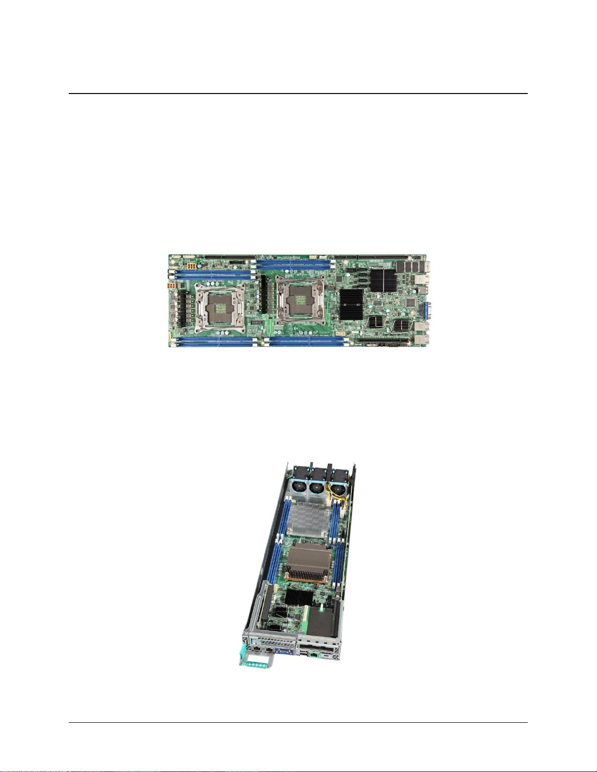
Figure 1. Intel® Server Board S2600KPFR (demo picture) ............................................................................. 3
Figure 2. Intel® Compute Module HNS2600KPR (demo picture) ................................................................ 3
Figure 3. Server Board Components (S2600KPFR).......................................................................................... 6
Figure 4. Compute Module Components ............................................................................................................. 6
Figure 5. Server Board Rear Connectors .............................................................................................................. 7
Figure 6. Compute Module Back Panel ................................................................................................................. 7
Figure 7. Intel® Light Guided Diagnostic LED ...................................................................................................... 8
Figure 8. Jumper Identification ................................................................................................................................ 8
Figure 9. Server Board Dimension .......................................................................................................................... 9
Figure 10. Compute Module Dimension ............................................................................................................... 9
Figure 11. Intel® Server Board S2600KPR Block Diagram .......................................................................... 11
Figure 12. Intel® Server Board S2600KPFR Block Diagram ........................................................................ 12
Figure 13. Intel® Server Board S2600KPTR Block Diagram ......................................................................... 13
Figure 14. Power Docking Board Overview ...................................................................................................... 14
Figure 15. 6G SATA Bridge Board Overview .................................................................................................... 15
Figure 16. 12G SAS Bridge Board with IT mode Overview ........................................................................ 15
Figure 17. 12G SAS Bridge Board with RAID 0, 1 and 10 Overview ....................................................... 16
Figure 18. 12G SAS Bridge Board with RAID 0, 1, 5 and 10 Overview .................................................. 16
Figure 19. Riser Card for Riser Slot #1 ............................................................................................................... 16
Figure 20. Riser Card for Riser Slot #2 ............................................................................................................... 17
Figure 21. I/O Module Carrier Installation ........................................................................................................ 17
Figure 22. Installing the M.2 Device .................................................................................................................... 18
Figure 23. AXXKPTPM2IOM I/O Module Carrier Connectors ................................................................... 18
Figure 24. Connecting the M.2 SATA cable ...................................................................................................... 19
Figure 25. Compute Module Fans ........................................................................................................................ 20
Figure 26. Air Duct ...................................................................................................................................................... 21
Figure 27. Intel® RAID C600 Upgrade Key ......................................................................................................... 21
Figure 28. Intel® RMM4 Lite ..................................................................................................................................... 22
Figure 29. Breakout Board Front and Rear View ............................................................................................ 23
Figure 30. Breakout Board Mechanical Drawing (Unit: mm)...................................................................... 23
Figure 31. Processor Socket Assembly .............................................................................................................. 30
Figure 32. Processor Socket ILM .......................................................................................................................... 30
Figure 33. Processor Heat Sink Overview ......................................................................................................... 38
Figure 34. Integrated Memory Controller Functional Block Diagram ................................................... 39
Figure 35. DIMM Slot Identification ..................................................................................................................... 44
x Revision 1.37
Page 11

Technical Product Specification List of Figures
Figure 36. Add-in Card Support Block Diagram (S2600KPR) ................................................................... 53
Figure 37. Server Board Riser Slots (S2600KPFR) ......................................................................................... 53
Figure 38. SATA Support ......................................................................................................................................... 55
Figure 39. SATA RAID 5 Upgrade Key................................................................................................................. 59
Figure 40. Network Interface Connectors ......................................................................................................... 60
Figure 41. RJ45 NIC Port LED................................................................................................................................. 61
Figure 42. USB Ports Block Diagram ................................................................................................................... 63
Figure 43. Serial Port A Location .......................................................................................................................... 63
Figure 44. Jumper Location .................................................................................................................................... 86
Figure 45. Status LED (E) and ID LED (D) ........................................................................................................... 94
Figure 46. InfiniBand* Link LED (K) and InfiniBand* Activity LED (J) ..................................................... 98
Figure 47. Rear Panel Diagnostic LEDs .............................................................................................................. 99
Figure 48. High-level Fan Speed Control Process ...................................................................................... 119
Figure 49. Air Flow and Fan Identification ..................................................................................................... 134
Figure 50. Turn On/Off Timing (Power Supply Signals – 5VSB) ........................................................... 148
Figure 51. Turn On/Off Timing (Power Supply Signals – 12VSB) ........................................................ 148
Figure 52. Diagnostic LED Placement Diagram ........................................................................................... 174
Revision 1.37 xi
Page 12

List of Tables Technical Product Specification
List of Tables
Table 1. Intel® Server Board S2600KP Product Family Feature Set .......................................................... 4
Table 2. Intel® Compute Module HNS2600KP Product Family Feature Set .......................................... 5
Table 3. Product Weight and Packaging ........................................................................................................... 10
Table 4. POST Hot-Keys ........................................................................................................................................... 26
Table 5. Mixed Processor Configurations Error Summary ......................................................................... 33
Table 6. DDR4-2400 DIMM Support Guidelines for Intel® Xeon processor v4 Product Family . 42
Table 8. DIMM Nomenclature ................................................................................................................................ 44
Table 9. Supported DIMM Populations .............................................................................................................. 44
Table 10. PCIe* Port Routing – CPU 1 ................................................................................................................ 54
Table 11. PCIe* Port Routing – CPU 2 ................................................................................................................ 54
Table 12. SATA and sSATA Controller BIOS Utility Setup Options ....................................................... 55
Table 13. SATA and sSATA Controller Feature Support ............................................................................ 56
Table 14. Onboard Video Resolution and Refresh Rate (Hz) .................................................................... 62
Table 15. Network Port Configuration ............................................................................................................... 64
Table 16. Main Power Supply Connector 6-pin 2x3 Connector .............................................................. 66
Table 17. Backup Power Connector .................................................................................................................... 66
Table 18. Intel® RMM4 Lite Connector ................................................................................................................ 67
Table 19. IPMB Header ............................................................................................................................................. 67
Table 20. Control Panel Connector ..................................................................................................................... 67
Table 21. Bridge Board Connector ...................................................................................................................... 68
Table 22. SATA DOM Connector Pin-out .......................................................................................................... 69
Table 23. USB 2.0 Type-A Connector Pin-out ................................................................................................ 70
Table 24. 5V_AUX Power Connector Pin-out.................................................................................................. 70
Table 25. CPU1 and CPU2 PCIe Bus Connectivity ......................................................................................... 70
Table 26. PCI Express* x16 Riser Slot 1 Connector ...................................................................................... 71
Table 27. PCI Express* x24 Riser Slot 2 Connector ...................................................................................... 73
Table 28. PCI Express* x24 Riser Slot 3 Connector ...................................................................................... 76
Table 29. PCI Express* Riser ID Assignment .................................................................................................... 78
Table 30. PCI Express* Clock Source by Slot .................................................................................................. 78
Table 31. VGA External Video Connector ......................................................................................................... 78
Table 32. RJ-45 10/100/1000 NIC Connector ............................................................................................... 79
Table 33. SATA Connector ...................................................................................................................................... 80
Table 34. SATA SGPIO Connector ....................................................................................................................... 80
Table 35. SATA HDD Activity LED Header ........................................................................................................ 80
Table 36. Storage Upgrade Key Connector ..................................................................................................... 81
xii Revision 1.37
Page 13

Technical Product Specification List of Tables
Table 37. Internal 9-pin Serial A ........................................................................................................................... 81
Table 38. External USB port Connector............................................................................................................. 81
Table 39. Internal USB Connector ....................................................................................................................... 81
Table 40. QSFP+ Connector ................................................................................................................................... 82
Table 41. UART Header ............................................................................................................................................ 82
Table 42. Baseboard Fan Connector................................................................................................................... 83
Table 43. Baseboard Fan Connector................................................................................................................... 83
Table 44. Main Power Input Connector ............................................................................................................. 84
Table 45. Fan Control Signal Connector ........................................................................................................... 84
Table 46. Compute Module Fan Connector ..................................................................................................... 84
Table 47. Main Power Output Connector ......................................................................................................... 84
Table 48. Miscellaneous Signal Connector ...................................................................................................... 85
Table 49. Jumper Modes Selection ..................................................................................................................... 86
Table 50. PS All Node off (J6B4) .......................................................................................................................... 87
Table 51. Force Integrated BMC Update Jumper (J6B6) ............................................................................ 87
Table 52. Force ME Update Jumper (J5D2) ..................................................................................................... 88
Table 53. Password Clear Jumper (J6B8) ......................................................................................................... 90
Table 54. BIOS Recovery Mode Jumper (J6B9) ............................................................................................. 91
Table 55. BIOS Default Jumper ............................................................................................................................. 92
Table 56. Status LED State Definitions .............................................................................................................. 95
Table 57. ID LED .......................................................................................................................................................... 97
Table 58. BMC Boot/Reset Status LED Indicators ......................................................................................... 97
Table 59. InfiniBand* Link/Activity LED ............................................................................................................. 98
Table 60. ACPI Power States ............................................................................................................................... 103
Table 61. Processor Sensors ............................................................................................................................... 111
Table 62. Processor Status Sensor Implementation ................................................................................. 112
Table 63. Component Fault LEDs ...................................................................................................................... 123
Table 64. Intel® Remote Management Module 4 (RMM4) Options ...................................................... 126
Table 65. Basic and Advanced Server Management Features Overview .......................................... 127
Table 66. Air Flow .................................................................................................................................................... 134
Table 67. TPM Setup Utility – Security Configuration Screen Fields ................................................. 140
Table 68. Server Board Design Specifications ............................................................................................. 141
Table 69. Power Supply DC Power Input Connector Pin-out ................................................................ 142
Table 70. Minimum 1200W/1600W Load Ratings..................................................................................... 142
Table 71. Minimum 2130W Load Ratings ...................................................................................................... 142
Table 72. Voltage Regulation Limits ................................................................................................................ 143
Table 73. Transient Load Requirements ........................................................................................................ 143
Revision 1.37 xiii
Page 14

List of Tables Technical Product Specification
Table 74. Capacitive Loading Conditions ....................................................................................................... 144
Table 75. Ripples and Noise ................................................................................................................................ 145
Table 76. Timing Requirements ......................................................................................................................... 146
Table 77. Timing Requirements (12VSB) ....................................................................................................... 147
Table 78. BMC Sensor Table ............................................................................................................................... 152
Table 79. BIOS Sensor and SEL Data ............................................................................................................... 167
Table 80. POST Code LED Example ................................................................................................................. 175
Table 81. MRC Fatal Error Codes ....................................................................................................................... 175
Table 82. MRC Progress Codes .......................................................................................................................... 176
Table 83. POST Progress Codes ........................................................................................................................ 177
Table 84. POST Error Codes and Messages.................................................................................................. 181
Table 85. POST Error Beep Codes .................................................................................................................... 183
Table 86. Glossary ................................................................................................................................................... 187
xiv Revision 1.37
Page 15

Technical Product Specification List of Tables
<This page is intentionally left blank.>
Revision 1.37 xv
Page 16

Page 17

Technical Product Specification Introduction
1 Introduction
This Technical Product Specification (TPS) provides specific information detailing the features,
functionality, and high-level architecture of the Intel® Server Board S2600KP product family
and the Intel® Compute Module HNS2600KP product family.
Design-level information related to specific server board components and subsystems can be
obtained by ordering External Product Specifications (EPS) or External Design Specifications
(EDS) related to this server generation. EPS and EDS documents are made available under
NDA with Intel and must be ordered through your local Intel representative. See the Reference
Documents section for a list of available documents.
1.1 Chapter Outline
This document is divided into the following chapters:
Chapter 1 – Introduction
Chapter 2 – Product Features Overview
Chapter 3 – Processor Support
Chapter 4 – Memory Support
Chapter 5 – Server Board I/O
Chapter 6 – Connector and Header
Chapter 7 – Configuration Jumpers
Chapter 8 – Intel
Chapter 9 – Platform Management
Chapter 10 – Thermal Management
Chapter 11 – System Security
Chapter 12 – Environmental Limits Specification
Chapter 13 – Power Supply Specification Guidelines
Appendix A – Integration and Usage Tips
Appendix B – Integrated BMC Sensor Tables
Appendix C – BIOS Sensors and SEL Data
Appendix D – POST Code Diagnostic LED Decoder
Appendix E – POST Code Errors
®
Light-Guided Diagnostics
Appendix F – Statement of Volatility
Glossary
Reference Documents
Revision 1.37 1
Page 18

Introduction Technical Product Specification
2
1.2 Server Board Use Disclaimer
Intel Corporation server boards contain a number of high-density VLSI (Very Large Scale
Integration) and power delivery components that need adequate airflow to cool. Intel ensures
through its own chassis development and testing that when Intel server building blocks are
used together, the fully integrated system will meet the intended thermal requirements of
these components. It is the responsibility of the system integrator who chooses not to use
Intel developed server building blocks to consult vendor datasheets and operating
parameters to determine the amount of air flow required for their specific application and
environmental conditions. Intel Corporation cannot be held responsible if components fail or
the server board does not operate correctly when used outside any of their published
operating or non-operating limits.
Revision 1.37
Page 19
Technical Product Specification Product Features Overview
2 Product Features Overview
The Intel® Server Board S2600KP product family is a monolithic printed circuit board (PCB)
assembly with features designed to support the high performance and high density
computing markets. This server board is designed to support the Intel® Xeon® processor E52600 v3/v4 product family. Previous generation Intel® Xeon® processors are not supported.
The Intel® Server Board S2600KP product family contains two server board options. Many of
the features and functions of the server board family are common. A board will be identified
by its name which has described features or functions unique to it.
S2600KPFR – With onboard InfiniBand* controller providing one external rear QSFP+
port
Figure 1. Intel® Server Board S2600KPFR (demo picture)
S2600KPR – Without onboard InfiniBand* controller, no external rear QSFP+ port
The Intel® Compute Module HNS2600KP product family provides two compute module
options, each integrated with either of the server board from the Intel® Server Board S2600KP
product family.
Figure 2. Intel® Compute Module HNS2600KPR (demo picture)
Revision 1.37 3
Page 20

Product Features Overview Technical Product Specification
4
Feature
Description
Processor Support
Two LGA2011-3 (Socket R3) processor sockets
Support for one or two Intel
®
Xeon® processors E5-2600 v3/v4
product family
Maximum supported Thermal Design Power (TDP) of up to 160 W
Memory Support
Eight DIMM slots in total across eight memory channels
Registered DDR4 (RDIMM), Load Reduced DDR4 (LRDIMM)
Memory DDR4 data transfer rates of 1600/1866/2133/2400 MT/s
Chipset
Intel® C612 chipset
External I/O Connections
DB-15 video connector
Two RJ-45 1GbE Network Interface Controller (NIC) ports
One dedicated RJ-45 port for remote server management
One stacked two port USB 2.0 (port 0/1) connector
One InfiniBand* FDR QSFP+ port (S2600KPFR only)
Internal I/O
connectors/headers
Bridge slot to extend board I/O
o Four SATA 6Gb/s signals to backplane
o Front control panel signals
o One SATA 6Gb/s port for SATA DOM
o One USB 2.0 connector (port 10)
One internal USB 2.0 connector (port 6/7)
One 2x7 pin header for system fan module
One 1x12 pin control panel header
One DH-10 serial Port A connector
One SATA 6Gb/s port for SATA DOM
Four SATA 6Gb/s connectors (port 0/1/2/3)
One 2x4 pin header for Intel
®
RMM4 Lite
One 1x4 pin header for Storage Upgrade Key
One 1x8 pin backup power connector
PCIe Support
PCIe* 3.0 (2.5, 5, 8 GT/s)
Power Connections
Two sets of 2x3 pin connectors (main power 1/2)
System Fan Support
One 2x7 pin fan control connector for Intel compute module and
chassis
Three 1x8 pin fan connectors for third-party chassis
Video
Integrated 2D video graphics controller
16MB DDR3 memory
Riser Support
Three riser slots
o Riser slot 1 provides x16 PCIe* 3.0 lanes
o Riser slot 2 provides
x24 PCIe* 3.0 lanes for S2600KPR
x16 PCIe* 3.0 lanes for S2600KPFR
o Riser slot 3 provides x24 PCIe* 3.0 lanes
One bridge board slot for board I/O expansion
The following table provides a high-level product feature list.
Table 1. Intel® Server Board S2600KP Product Family Feature Set
Revision 1.37
Page 21

Technical Product Specification Product Features Overview
Feature
Description
On-board storage
controllers and options
5 on-board SATA 6Gb/s ports, one of them is SATA DOM compatible.
5 SATA 6Gb/s signals to backplane via bridge slot.
RAID Support
Intel
®
Rapid Storage RAID Technology (RSTe) 4.0
Intel
®
Embedded Server RAID Technology 2 (ESRT2) with optional
Intel® RAID C600 Upgrade Key to enable SATA RAID 5
Server Management
Onboard Emulex* Pilot III* Controller
Support for Intel
®
Remote Management Module 4 Lite solutions
Intel
®
Light-Guided Diagnostics on field replaceable units
Support for Intel
®
System Management Software
Support for Intel
®
Intelligent Power Node Manager (Need
PMBus*-compliant power supply)
Security
Intel® Trusted Platform Module (TPM) v1.2 for BBS2600KPTR only
Feature1
Description
Server Board
Intel® Server Board S2600KP product family
HNS2600KPR – include Intel
®
Server Board S2600KPR
HNS2600KPFR – include Intel
®
Server Board S2600KPFR
Processor Support
Maximum supported Thermal Design Power (TDP) of up to 145 W
Heat Sink
One Cu/Al 91.5x91.5mm heat sink for CPU 1
One Ex-Al 91.5x91.5mm heat sink for CPU 2
Fan
Three sets of 40x56mm dual rotor system fans
Riser Support
One riser card with bracket on riser slot 1 to support one PCIe* 3.0
x16 low profile card (default)2
One I/O module riser and carrier kit on riser slot 2 to support an
Intel® I/O Expansion Module (optional)
Note: Riser slot 3 cannot be used with the bridge board installed.
Compute Module Board
Three types of bridge boards:
o 6G SATA Bridge Board (Default)
o 12G SAS Bridge Board (Optional)
o 12G SAS Bridge Board with RAID 5 (Optional)
One compute module power docking board
Air Duct
One transparent air duct
Warning! The riser slot 1 on the server board is designed for plugging in ONLY the riser card.
Plugging in any PCIe* card may cause permanent server board and PCIe* card damage.
Table 2. Intel® Compute Module HNS2600KP Product Family Feature Set
Notes:
1. The table only lists features that are unique to the compute module or different from the
server board.
Revision 1.37 5
Page 22
Product Features Overview Technical Product Specification
6
2. ONLY low profile PCIe* card can be installed on riser slot 1 riser card of the compute
module.
2.1 Components and Features Identification
This section provides a general overview of the server board and compute module, identifying
key features and component locations. The majority of the items identified are common in the
product family.
Figure 3. Server Board Components (S2600KPFR)
Figure 4. Compute Module Components
Revision 1.37
Page 23
Technical Product Specification Product Features Overview
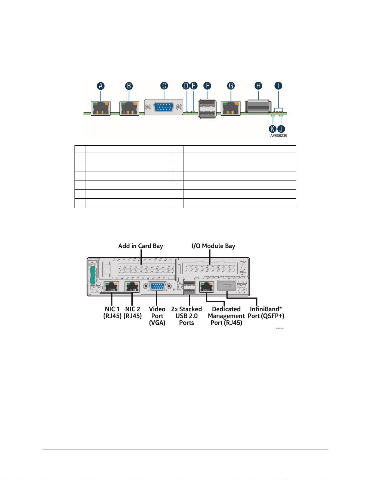
Description
Description
A
NIC port 1 (RJ45)
G
Dedicated Management Port (RJ45)
B
NIC port 2 (RJ45)
H
InfiniBand* Port (QSFP+, S2600KPFR only)
C
Video out (DB-15)
I
POST Code LEDs (8 LEDs)
D
ID LED
J
InfiniBand* Activity LED (S2600KPFR only)
E
Status LED
K
InfiniBand* Link LED (S2600KPFR only)
F
Dual port USB
2.2 Rear Connectors and Back Panel Feature Identification
The Intel® Server Board S2600KP product family has the following board rear connector
placement.
Figure 5. Server Board Rear Connectors
The Intel® Compute Module HNS2600KP product family has the following back panel features.
Figure 6. Compute Module Back Panel
Revision 1.37 7
Page 24
Product Features Overview Technical Product Specification
8
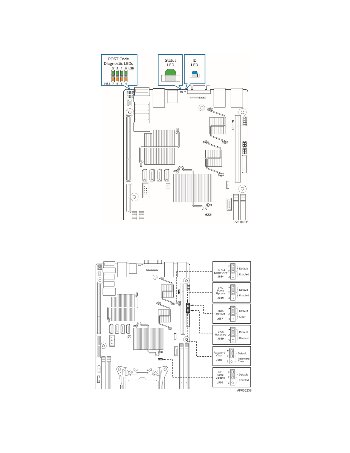
2.3 Intel
®
Light Guided Diagnostic LED
Figure 7. Intel® Light Guided Diagnostic LED
2.4 Jumper Identification
Figure 8. Jumper Identification
Revision 1.37
Page 25
Technical Product Specification Product Features Overview
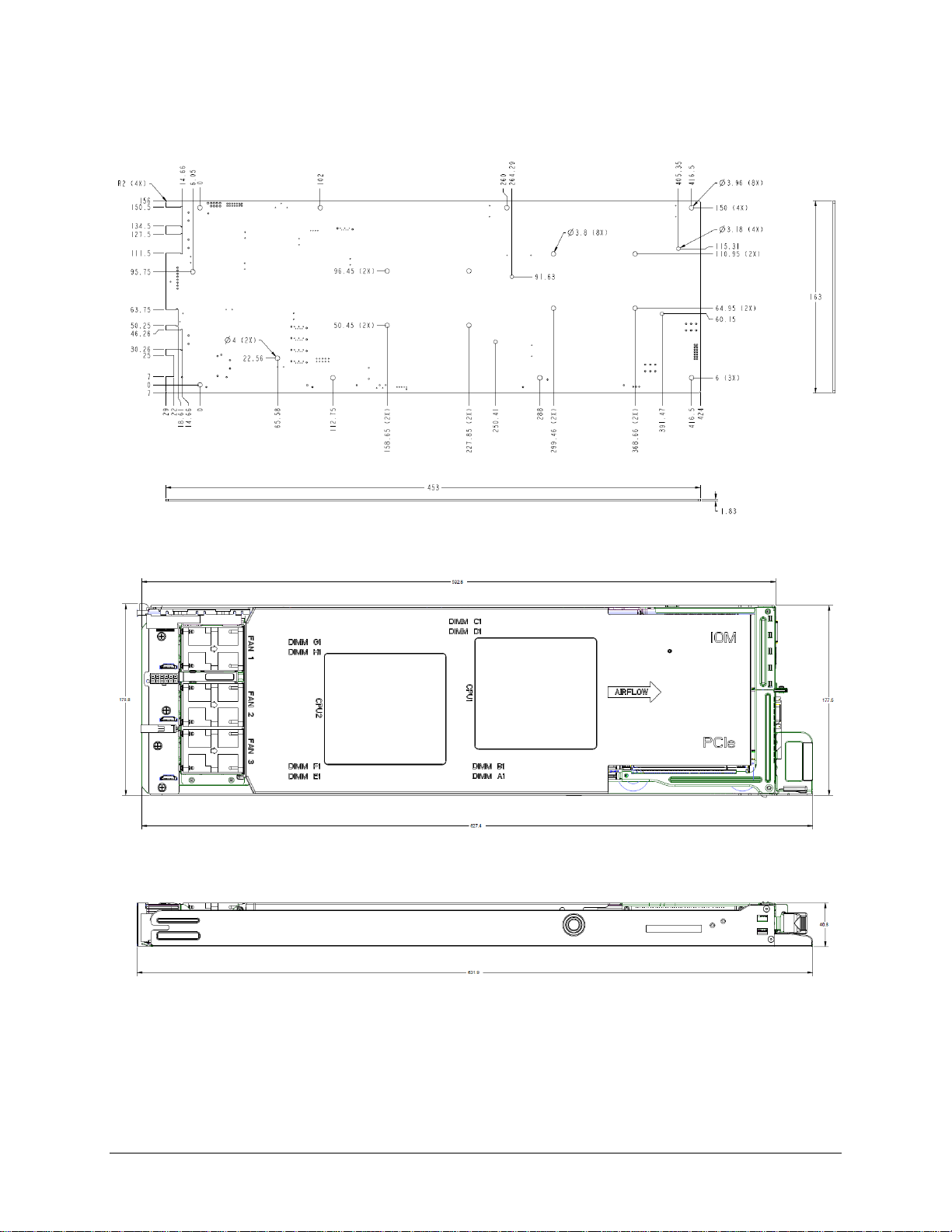
2.5 Mechanical Dimension and Weight
Figure 9. Server Board Dimension
Figure 10. Compute Module Dimension
Revision 1.37 9
Page 26
Product Features Overview Technical Product Specification
10
Product Code
Quantity per Box
Box Dimension (mm)
Net Weight
Package Weight
BBS2600KPR
10
553X242X463
10.0 kg
12.8 kg
BBS2600KPFR
10
553X242X463
10.4 kg
13.2 kg
BBS2600KPTR
10
553X242X463
0.98 kg
12.6 kg
HNS2600KPR
1
716X269X158
3.4 kg
4.6 kg
HNS2600KPFR
1
716X269X158
3.44 kg
4.64 kg
Approximate product weight is listed in the following table for reference. Variations are
expected with real shipping products.
Table 3. Product Weight and Packaging
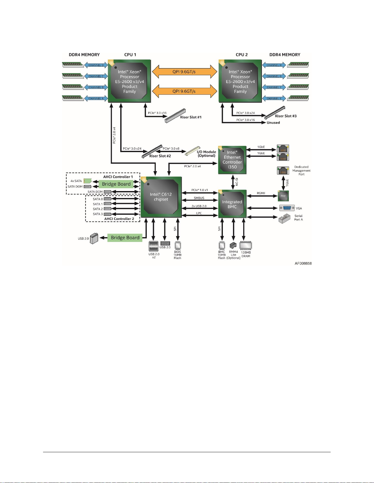
2.6 Product Architecture Overview
The Intel® Server Board S2600KP product family is a purpose built, rack-optimized, liquid
cooling friendly server board used in a high-density rack system. It is designed around the
integrated features and functions of the Intel® Xeon® processor E5-2600 V3/V4 product family,
the Intel® C612 chipset, and other supporting components including the Integrated BMC, the
Intel® I350 network interface controller, and the Mellanox* Connect-IB* adapter (S2600KPFR
only).
The half-width board size allows four boards to reside in a standard multi-compute module
2U Intel® Server Chassis H2000G product family, for high-performance and high-density
computing platforms.
The following diagram provides an overview of the server board architecture, showing the
features and interconnects of each of the major subsystem components.
Revision 1.37
Page 27
Technical Product Specification Product Features Overview
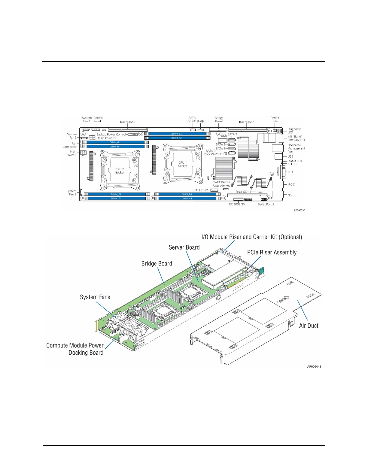
Figure 11. Intel® Server Board S2600KPR Block Diagram
Revision 1.37 11
Page 28
Product Features Overview Technical Product Specification
12
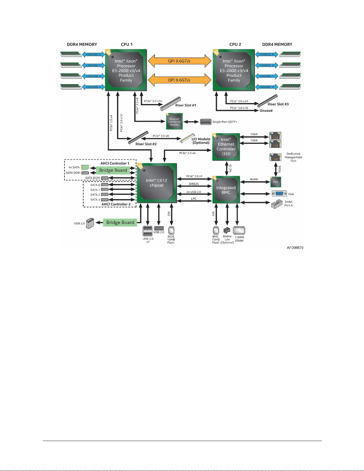
Figure 12. Intel® Server Board S2600KPFR Block Diagram
Revision 1.37
Page 29
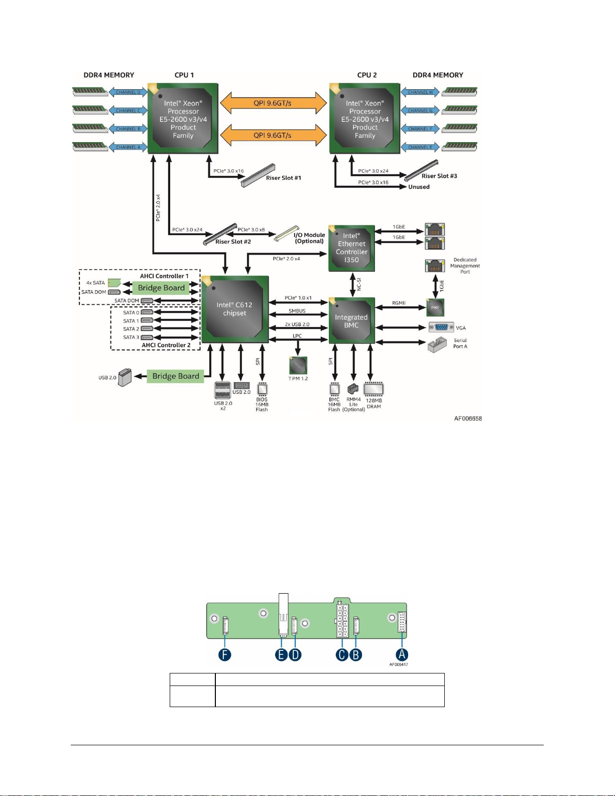
Technical Product Specification Product Features Overview
Label
Description
A
2x7-pin fan control connector
Figure 13. Intel® Server Board S2600KPTR Block Diagram
The Intel® Compute Module HNS2600KP product family provides a series of features including
the power docking board, bridge boards, riser cards, fans, and the air duct.
2.7 Power Docking Board
The power docking board provides hot swap docking of 12V main power between the
compute module and the server. It supports three dual rotor fan connections, 12V main power
hot swap controller, and current sensing. The power docking board is intended to support the
usage of the compute module with the Intel® Server Board S2600KP product family.
Revision 1.37 13
Page 30
Product Features Overview Technical Product Specification
14
B
8-pin connector for fan 1
C
2x6-pin main power output connector
D
8-pin connector for fan 2
E
12-pin connector for main power input
F
8-pin connector for fan 3
Label
Description
A
2x40-pin card edge connector (to the backplane)
B
USB 2.0 Type-A connector
C
2-pin 5V power
D
SATA DOM port connector
Figure 14. Power Docking Board Overview
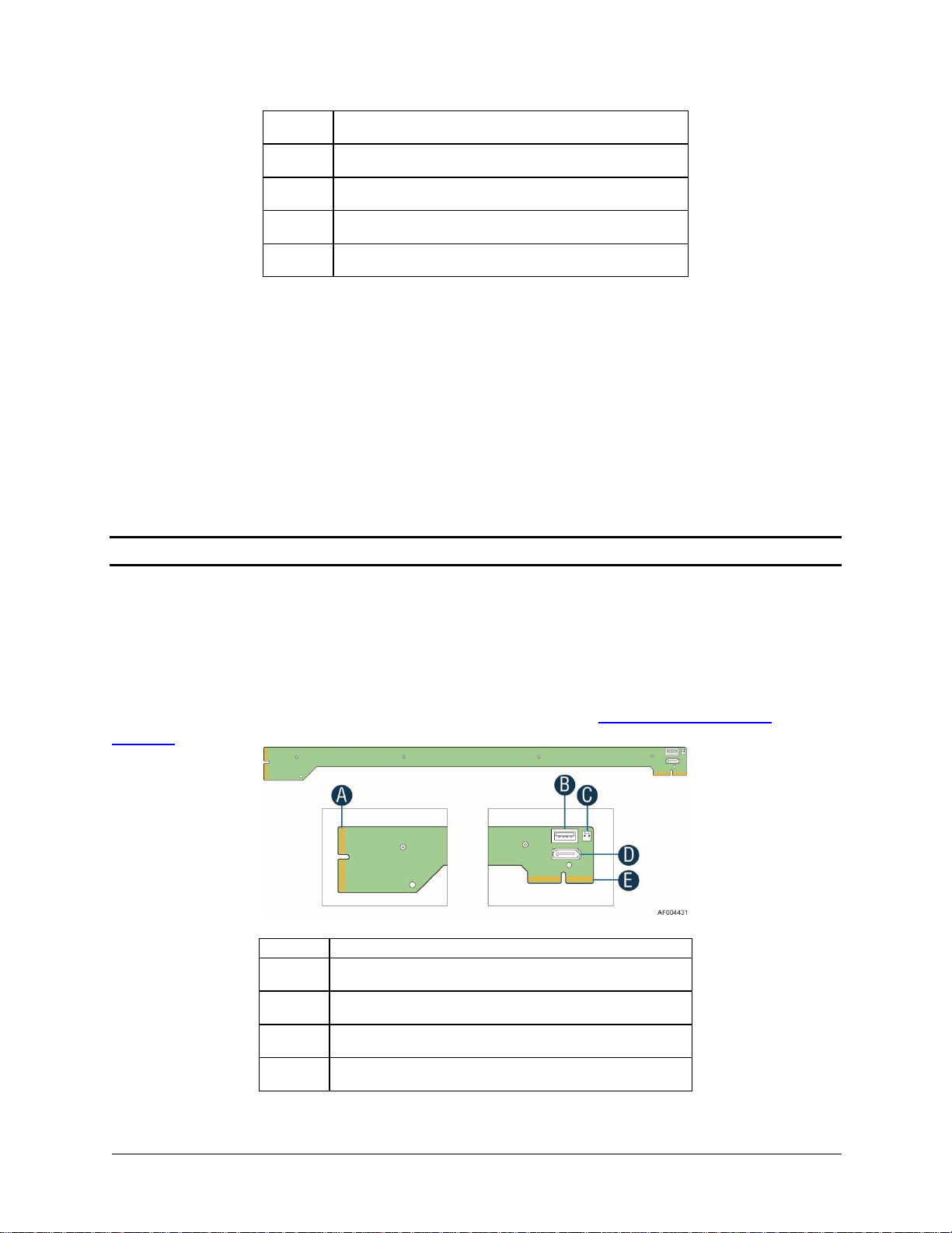
2.8 Bridge Board
There are four types of bridge boards that implement different features and functions.
6G SATA bridge board (Default)
12G SAS bridge board with IT mode (Optional)
12G SAS bridge board with RAID 0, 1 and 10 (Optional)
12G SAS bridge board with RAID 0, 1, 5 and 10 (Optional)
Note: All 12G SAS bridge boards require two processors installed to be functional.
2.8.1 6G SATA Bridge Board
The 6G SATA bridge board provides hot swap interconnect of all electrical signals to the
backplane of the server chassis (except for main 12V power). It supports up to 4x lanes of
SATA, a 7-pin SATA connector for SATA DOM devices, and a type-A USB connector for USB
flash device. One bridge board is used per one compute module. The bridge board is secured
with screws to the compute module. The bridge board support embedded SATA RAID
Support.
Revision 1.37
Page 31

Technical Product Specification Product Features Overview
Label
Description
E
2x40-pin card edge connector (to the bridge board
connector on the server board)
Label
Description
A
2x40-pin card edge connector (to the backplane)
B
UART header
C
2-pin 5V power
D
SATA DOM port connector
E
2x40-pin card edge connector (to the bridge board
connector on the server board)
F
200-pin connector (to Riser Slot 3 on the server board)
Label
Description
A
2x40-pin card edge connector (to the backplane)
B
UART header
C
2-pin 5V power
D
SATA DOM port connector
Figure 15. 6G SATA Bridge Board Overview
2.8.2 12G SAS Bridge Board with IT mode
The optional 12G SAS bridge board with IT mode has one embedded LSI* SAS 3008 controller
to support up to four SAS/SATA, a 7-pin SATA connector for SATA DOM devices, and a UART
(Universal Asynchronous Receiver/Transmitter) header. One bridge board is used per one
compute module, connecting to the bridge board slot and Riser Slot 3.
Figure 16. 12G SAS Bridge Board with IT mode Overview
2.8.3 12G SAS Bridge Board with RAID 0, 1 and 10
The optional 12G SAS bridge board has one embedded LSI* SAS 3008 controller to support
up to four SAS/SATA ports with RAID 0, 1, and 10 support, a 7-pin SATA connector for SATA
DOM devices, and a type-A USB connector for USB flash device. One bridge board is used per
one compute module, connecting to the bridge board slot and Riser Slot 3.
Revision 1.37 15
Page 32

Product Features Overview Technical Product Specification
16
E
2x40-pin card edge connector (to the bridge board
connector on the server board)
F
200-pin connector (to Riser Slot 3 on the server board)
Label
Description
A
2x40-pin card edge connector (to the backplane)
B
UART header
C
2-pin 5V power
D
SATA DOM port connector
E
2x40-pin card edge connector (to the bridge board
connector on the server board)
F
200-pin connector (to Riser Slot 3 on the server board)
Figure 17. 12G SAS Bridge Board with RAID 0, 1 and 10 Overview
2.8.4 12G SAS Bridge Board with RAID 0, 1, 5 and 10
The optional 12G SAS bridge board with RAID 5 has one embedded LSI* SAS 3008 controller
to support up to four SAS/SATA ports with RAID 0, 1, 10, and RAID 5 support, a 7-pin SATA
connector for SATA DOM devices, and a UART (Universal Asynchronous Receiver/Transmitter)
header. One bridge board is used per one compute module, connecting to the bridge board
slot and Riser Slot 3.
Figure 18. 12G SAS Bridge Board with RAID 0, 1, 5 and 10 Overview
2.9 Riser Card
There are two types of riser cards:
Riser slot 1 riser card (for Riser slot 1 only)
Riser slot 2 riser card (for Riser slot 2 only)
2.9.1 Riser Slot 1 Riser Card
The riser card for riser slot 1 has one PCIe* 3.0 x16 slot.
Figure 19. Riser Card for Riser Slot #1
Revision 1.37
Page 33

Technical Product Specification Product Features Overview
I/O Module Carrier
M.2 Support
Supported Computer Modules
AXXKPTPM2IOM
Yes
HNS2600KPR
AXXKPTPIOM
No
HNS2600KPR
HNS2600KPFR
2.9.2 Riser Slot 2 Riser Card
The riser card for riser slot 2 has one PCIe* 3.0 x16 slot (x8 lanes are for I/O module carrier)
which can only support Intel® I/O Module carrier.
Figure 20. Riser Card for Riser Slot #2
2.10 I/O Module Carrier
To broaden the standard on-board feature set, the server board supports the option of adding
a single I/O module providing external ports for a variety of networking interfaces. The I/O
module attaches to a high density 80-pin connector of the I/O module carrier on the riser slot
2 riser card.
Figure 21. I/O Module Carrier Installation
The I/O module carrier board is included in the optional accessory kit. It is
horizontallyinstalled to the riser slot 2 riser card. The board provides electrical connectivity for
installing an Intel® I/O Expansion Module and a SATA based M.2 form factor (NGFF, Next
Generation Form Factor) storage device. It supports up to x8 lanes of PCIe* 3.0 for the I/O
module, and a 7 pin SATA header for the M.2 device. The I/O module carrier has two types
AXXKPTPM2IOM and AXXKPTPIOM, only AXXKPTPM2IOM can support SATA based M.2. But
due to mechanical limitation, the AXXKPTPM2IOM cannot support the computer module with
onboard IB* module.
Revision 1.37 17
Page 34

Product Features Overview Technical Product Specification
18
A
2x40 pin Messanine connector (for I/O module)
B
7 pin SATA connector (to server board, for M.2 device)
The M.2 slot is on the backside of the AXXKPTPM2IOM, it can support M.2 2280 SSD which
size is 80.0 mm X 22.0 mm X 3.8 mm. User can install the M.2 device to the M.2 slot (See the
letter A on Figure 22) and fix it with the screw (See the letter B on the Figure 22).
Figure 22. Installing the M.2 Device
User still needs to connect the SATA connector (see B on Figure 23) on the AXXKPTPM2IOM
to the STAT connector on the server with SATA cable.
Figure 23. AXXKPTPM2IOM I/O Module Carrier Connectors
Revision 1.37
Page 35

Technical Product Specification Product Features Overview
Figure 24. Connecting the M.2 SATA cable
Revision 1.37 19
Page 36

Product Features Overview Technical Product Specification
20
2.11 Compute Module Fans
The cooling subsystem for the compute module consists of three 40 x 40 x 56 dual rotor fans.
These components provide the necessary cooling and airflow.
Figure 25. Compute Module Fans
Note: The Intel® Compute Module HNS2600KP product family does not support redundant
cooling. If one of the compute module fans fails, it is recommended to replace the failed fan as
soon as possible.
Each fan within the compute module can support multiple speeds. Fan speed may change
automatically when any temperature sensor reading changes. The fan speed control algorithm
is programmed into the server board’s BMC.
Each fan connector within the module supplies a tachometer signal that allows the BMC to
monitor the status of each fan. If one of the fans fails, the status LED on the server board will
light up.
The fan control signal is from the BMC on the mother board to the power docking board and
then is distributed to three sets of dual rotor fans. The expected maximum RPM is 25,000.
2.12 Air Duct
Each compute module requires the use of a transparent plastic air duct to direct airflow over
critical areas within the compute module. To maintain the necessary airflow, the air duct must
be properly installed. Before sliding the compute module into the chassis, make sure the air
duct is installed properly.
Revision 1.37
Page 37

Technical Product Specification Product Features Overview
Figure 26. Air Duct
2.13 Intel
The Intel® RAID C600 Upgrade Key RKSATA4R5 is supported. With the optional key installed
on the server board, Intel® ESRT2 SATA RAID 5 is enabled.
2.14 Intel
®
RAID C600 Upgrade Key
Figure 27. Intel® RAID C600 Upgrade Key
®
Remote Management Module 4 (Intel® RMM4) Lite
The optional Intel® RMM4 Lite is a small board that unlocks the advanced management
features when installed on the server board.
Revision 1.37 21
Page 38

Product Features Overview Technical Product Specification
22
Label
Description
A
SATA DOM port connector
B
Mini-SAS connector
Figure 28. Intel® RMM4 Lite
2.15 Breakout Board
Intel provides a breakout board which is designed for the server board only I/O peripherals in
a third-party chassis. It is not a standard accessory of the Intel® Compute Module HNS2600KP
product family or Intel® Server Chassis H2000G product family.
The breakout board provides:
One 7 pin SATA connector for 6Gb/s SATA DOM
One mini-SAS HD SFF-8643 connector for 4x lanes of 6Gb/s SATA
One 7 pin connector for miscellaneous signals:
o Status LED
o NMI switch
o SMBus
o 3.3V auxiliary power (maximum current 50mA)
Revision 1.37
Page 39

Technical Product Specification Product Features Overview
Label
Description
C
7 pin miscellaneous signals connector
Figure 29. Breakout Board Front and Rear View
The breakout board has reserved holes for users to design their own bracket to fix the board
into the server system. See the following mechanical drawing for details.
2.16 System Software Overview
The server board includes an embedded software stack to enable, configure, and support
various system functions. This software stack includes the System BIOS, Baseboard
Management Controller (BMC) Firmware, Management Engine (ME) Firmware, and
management support data including Field Replaceable Unit (FRU) data and Sensor Data
Record (SDR) data.
The system software is pre-programmed on the server board during factory assembly, making
the server board functional at first power-on after system integration. Typically, as part of the
initial system integration process, FRU and SDR data will have to be installed onto the server
board by the system integrator to ensure the embedded platform management subsystem is
Revision 1.37 23
Figure 30. Breakout Board Mechanical Drawing (Unit: mm)
Page 40

Product Features Overview Technical Product Specification
24
able to provide best performance and cooling for the final system configuration. It is also not
uncommon for the system software stack to be updated to later revisions to ensure the most
reliable system operation. Intel makes periodic system software updates available for
download at the following Intel website: http://downloadcenter.intel.com.
System updates can be performed in a number of operating environments, including the uEFI
Shell using the uEFI-only System Update Package (SUP), or under different operating systems
using the Intel® One Boot Flash Update Utility (OFU).
Reference the following Intel documents for more in-depth information about the system
software stack and their functions:
Intel
®
Server System BIOS External Product Specification for Intel® Server Systems
supporting the Intel® Xeon® processor E5-2600 v3/v4 product family
Intel
®
Server System BMC Firmware External Product Specification for Intel® Server
Systems supporting the Intel® Xeon® processor E5-2600 v3/v4 product family
2.16.1 System BIOS
The system BIOS is implemented as firmware that resides in flash memory on the server
board. The BIOS provides hardware-specific initialization algorithms and standard compatible
basic input/output services, and standard Intel® Server Board features. The flash memory also
contains firmware for certain embedded devices.
This BIOS implementation is based on the Extensible Firmware Interface (EFI), according to the
Intel® Platform Innovation Framework for EFI architecture, as embodied in the industry
standards for Unified Extensible Firmware Interface (UEFI).
The implementation is compliant with all Intel® Platform Innovation Framework for EFI
architecture specifications, as further specified in the Unified Extensible Firmware Interface
Reference Specification, Version 2.3.1.
In the UEFI BIOS design, there are three primary components: the BIOS itself, the Human
Interface Infrastructure (HII) that supports communication between the BIOS and external
programs, and the Shell which provides a limited OS-type command-line interface. This BIOS
system implementation complies with HII Version 2.3.1, and includes a Shell.
2.16.1.1 BIOS Revision Identification
The BIOS Identification string is used to uniquely identify the revision of the BIOS being used
on the server. The BIOS ID string is displayed on the Power On Self Test (POST) Diagnostic
Screen and in the <F2> BIOS Setup Main Screen, as well as in System Management BIOS
(SMBIOS) structures.
The BIOS ID string for S2600 series server boards is formatted as follows:
BoardFamilyID.OEMID.MajorVer.MinorVer.RelNum.BuildDateTime
Revision 1.37
Page 41

Technical Product Specification Product Features Overview
Where:
BoardFamilyID = String name to identify board family.
o “SE5C610” is used to identify BIOS builds for Intel
®
S2600 series Server Boards,
based on the Intel® Xeon® Processor E5-2600 product families and the Intel® C610
chipset family.
OEMID = Three-character OEM BIOS Identifier, to identify the board BIOS “owner”.
o “86B” is used for Intel Commercial BIOS Releases.
MajorVer = Major Version, two decimal digits 01-99 which are changed only to identify
major hardware or functionality changes that affect BIOS compatibility between
boards.
o “01” is the starting BIOS Major Version for all platforms.
MinorVer = Minor Version, two decimal digits 00-99 which are changed to identify less
significant hardware or functionality changes which do not necessarily cause
incompatibilities but do display differences in behavior or in support of specific
functions for the board.
RelNum = Release Number, four decimal digits which are changed to identify distinct
BIOS Releases. BIOS Releases are collections of fixes and/or changes in functionality,
built together into a BIOS Update to be applied to a Server Board. However, there are
“Full Releases” which may introduce many new fixes/functions, and there are “Point
Releases” which may be built to address very specific fixes to a Full Release.
The Release Numbers for Full Releases increase by 1 for each release. For Point
Releases, the first digit of the Full Release number on which the Point Release is based
is increased by 1. That digit is always 0 (zero) for a Full Release.
BuildDateTime = Build timestamp – date and time in MMDDYYYYHHMM format:
o MM = Two-digit month.
o DD = Two-digit day of month.
o YYYY = Four-digit year.
o HH = Two-digit hour using 24-hour clock.
o MM = Two-digit minute.
An example of a valid BIOS ID String is as follows:
SE5C610.86B.01.01.0003.081320110856
The BIOS ID string is displayed on the POST diagnostic screen for BIOS Major Version 01,
Minor Version 01, Full Release 0003 that is generated on August 13, 2011 at 8:56 AM.
The BIOS version in the <F2> BIOS Setup Utility Main Screen is displayed without the
time/date timestamp, which is displayed separately as “Build Date”:
SE5C610.86B.01.01.0003
Revision 1.37 25
Page 42

Product Features Overview Technical Product Specification
26
HotKey Combination
Function
<F2>
Enter the BIOS Setup Utility
<F6>
Pop-up BIOS Boot Menu
<F12>
Network boot
<Esc>
Switch from Logo Screen to Diagnostic Screen
<Pause>
Stop POST temporarily
2.16.1.2 Hot Keys Supported During POST
Certain “Hot Keys” are recognized during POST. A Hot Key is a key or key combination that is
recognized as an unprompted command input, that is, the operator is not prompted to press
the Hot Key and typically the Hot Key will be recognized even while other processing is in
progress.
The BIOS recognizes a number of Hot Keys during POST. After the OS is booted, Hot Keys are
the responsibility of the OS and the OS defines its own set of recognized Hot Keys.
The following table provides a list of available POST Hot Keys along with a description for
each.
Table 4. POST Hot-Keys
2.16.1.3 POST Logo/Diagnostic Screen
The Logo/Diagnostic Screen appears in one of two forms:
If Quiet Boot is enabled in the <F2> BIOS setup, a “splash screen” is displayed with a
logo image, which may be the standard Intel Logo Screen or a customized OEM Logo
Screen. By default, Quiet Boot is enabled in BIOS setup, so the Logo Screen is the
default POST display. However, if the logo is displayed during POST, the user can
press <Esc> to hide the logo and display the Diagnostic Screen instead.
If a customized OEM Logo Screen is present in the designated Flash Memory location,
the OEM Logo Screen will be displayed, overriding the default Intel Logo Screen.
If a logo is not present in the BIOS Flash Memory space, or if Quiet Boot is disabled in
the system configuration, the POST Diagnostic Screen is displayed with a summary of
system configuration information. The POST Diagnostic Screen is purely a Text Mode
screen, as opposed to the Graphics Mode logo screen.
If Console Redirection is enabled in Setup, the Quiet Boot setting is disregarded and
the Text Mode Diagnostic Screen is displayed unconditionally. This is due to the
limitations of Console Redirection, which transfers data in a mode that is not
graphics-compatible.
2.16.1.4 BIOS Boot Pop-Up Menu
The BIOS Boot Specification (BBS) provides a Boot Pop-up menu that can be invoked by
pressing the <F6> key during POST. The BBS Pop-up menu displays all available boot devices.
Revision 1.37
Page 43

Technical Product Specification Product Features Overview
The boot order in the pop-up menu is not the same as the boot order in the BIOS setup. The
pop-up menu simply lists all of the available devices from which the system can be booted,
and allows a manual selection of the desired boot device.
When an Administrator password is installed in Setup, the Administrator password will be
required in order to access the Boot Pop-up menu using the <F6> key. If a User password is
entered, the Boot Pop-up menu will not even appear – the user will be taken directly to the
Boot Manager in the Setup, where a User password allows only booting in the order previously
defined by the Administrator.
2.16.1.5 Entering BIOS Setup
To enter the BIOS Setup Utility using a keyboard (or emulated keyboard), press the <F2>
function key during boot time when the OEM or Intel Logo Screen or the POST Diagnostic
Screen is displayed.
The following instructional message is displayed on the Diagnostic Screen or under the Quiet
Boot Logo Screen:
Press <F2> to enter setup, <F6> Boot Menu, <F12> Network Boot
Note: With a USB keyboard, it is important to wait until the BIOS “discovers” the keyboard and
beeps – until the USB Controller has been initialized and the USB keyboard activated, key
presses will not be read by the system.
When the Setup Utility is entered, the Main screen is displayed initially. However, in the event
a serious error occurs during POST, the system will enter the BIOS Setup Utility and display
the Error Manager screen instead of the Main screen.
2.16.1.6 BIOS Update Capability
In order to bring BIOS fixes or new features into the system, it will be necessary to replace the
current installed BIOS image with an updated one. The BIOS image can be updated using a
standalone IFLASH32 utility in the uEFI shell, or can be done using the OFU utility program
under a given operating system. Full BIOS update instructions are provided when update
packages are downloaded from the Intel web site.
2.16.1.7 BIOS Recovery
If a system is completely unable to boot successfully to an OS, hangs during POST, or even
hangs and fails to start executing POST, it may be necessary to perform a BIOS Recovery
procedure, which can replace a defective copy of the Primary BIOS.
The BIOS introduces three mechanisms to start the BIOS recovery process, which is called
Recovery Mode:
Recovery Mode Jumper – This jumper causes the BIOS to boot in Recovery Mode.
Revision 1.37 27
Page 44

Product Features Overview Technical Product Specification
28
The Boot Block detects partial BIOS update and automatically boots in Recovery
Mode.
The BMC asserts Recovery Mode GPIO in case of partial BIOS update and FRB2
time-out.
The BIOS Recovery takes place without any external media or Mass Storage device as it
utilizes a Backup BIOS image inside the BIOS flash in Recovery Mode.
The Recovery procedure is included here for general reference. However, if in conflict, the
instructions in the BIOS Release Notes are the definitive version.
When the BIOS Recovery Jumper (see Figure 38) is set, the BIOS begins by logging a “Recovery
Start” event to the System Event Log (SEL). It then loads and boots with a Backup BIOS image
residing in the BIOS flash device. This process takes place before any video or console is
available. The system boots to the embedded uEFI shell, and a “Recovery Complete” event is
logged to the SEL. From the uEFI Shell, the BIOS can then be updated using a standard BIOS
update procedure, defined in Update Instructions provided with the system update package
downloaded from the Intel web site. Once the update has completed, the recovery jumper is
switched back to its default position and the system is power cycled.
If the BIOS detects a partial BIOS update or the BMC asserts Recovery Mode GPIO, the BIOS
will boot up with Recovery Mode. The difference is that the BIOS boots up to the Error
Manager Page in the BIOS Setup utility. In the BIOS Setup utility, boot device, Shell or Linux for
example, could be selected to perform the BIOS update procedure under Shell or OS
environment.
2.16.2 Field Replaceable Unit (FRU) and Sensor Data Record (SDR) Data
As part of the initial system integration process, the server board/system must have the
proper FRU and SDR data loaded. This ensures that the embedded platform management
system is able to monitor the appropriate sensor data and operate the system with best
cooling and performance. The BMC supports automatic configuration of the manageability
subsystem after changes have been made to the system’s hardware configuration. Once the
system integrator has performed an initial SDR/CFG package update, subsequent
auto-configuration occurs without the need to perform additional SDR updates or provide
other user input to the system when any of the following components are added or removed.
Processors
I/O Modules (dedicated slot modules)
Storage modules such as a SAS module (dedicated slot modules)
Power supplies
Fans
Fan options (e.g. upgrade from non-redundant cooling to redundant cooling)
Intel
®
Xeon Phi™ co-processor cards
Hot Swap Backplane
Revision 1.37
Page 45

Technical Product Specification Product Features Overview
Front Panel
Note: The system may not operate with best performance or best/appropriate cooling if the
proper FRU and SDR data is not installed.
2.16.2.1 Loading FRU and SDR Data
The FRU and SDR data can be updated using a standalone FRUSDR utility in the uEFI shell, or
can be done using the OFU utility program under a given operating system. Full FRU and SDR
update instructions are provided with the appropriate system update package (SUP) or OFU
utility which can be downloaded from the Intel web site.
2.16.3 Baseboard Management Controller (BMC) Firmware
See Platform Management chapter.
Revision 1.37 29
Page 46

Processor Support Technical Product Specification
30
3 Processor Support
The server board includes two Socket-R3 (LGA 2011-3) processor sockets and can support
one or two of the Intel® Xeon® processor E5-2600 v3/v4 product family, with a Thermal Design
Power (TDP) of up to 160W.
Note: Previous generation Intel® Xeon® processors are not supported on the Intel® Server Boards
described in this document.
Visit http://www.intel.com/support for a complete list of supported processors.
3.1 Processor Socket Assembly
Each processor socket of the server board is pre-assembled with an Independent Latching
Mechanism (ILM) and Back Plate which allow for secure placement of the processor and
processor heat to the server board.
The following illustration identifies each sub-assembly component.
Figure 31. Processor Socket Assembly
Figure 32. Processor Socket ILM
Revision 1.37
Page 47

Technical Product Specification Processor Support
The square ILM has an 80 x 80mm heat sink mounting hole pattern.
Note: The pins inside the CPU socket are extremely sensitive. Other than the CPU, no object
should make contact with the pins inside the CPU socket. A damaged CPU Socket pin may
render the socket inoperable, and will produce erroneous CPU or other system errors if
used.
3.2 Processor Thermal Design Power (TDP) Support
To allow optimal operation and long-term reliability of Intel processor-based systems, the
processor must remain within the defined minimum and maximum case temperature (TCASE)
specifications. Thermal solutions not designed to provide sufficient thermal capability may
affect the long-term reliability of the processor and system. The server board described in this
document is designed to support the Intel® Xeon® Processor E5-2600 v3/v4 product family
TDP guidelines up to and including 160W. The compute module described in this document is
designed to support the Intel® Xeon® Processor E5-2600 v3/v4 product family TDP guidelines
up to and including 145W.
Disclaimer Note: Intel Corporation server boards contain a number of high-density VLSI and
power delivery components that need adequate airflow to cool. Intel ensures through its own
chassis development and testing that when Intel server building blocks are used together, the
fully integrated system will meet the intended thermal requirements of these components. It is
the responsibility of the system integrator who chooses not to use Intel developed server
building blocks to consult vendor datasheets and operating parameters to determine the
amount of airflow required for their specific application and environmental conditions. Intel
Corporation cannot be held responsible if components fail or the server board does not
operate correctly when used outside any of their published operating or non-operating limits.
3.3 Processor Population Rules
Note: The server board may support dual-processor configurations consisting of different
processors that meet the defined criteria below, however, Intel does not perform validation
testing of this configuration. In addition, Intel does not guarantee that a server system
configured with unmatched processors will operate reliably. The system BIOS will attempt to
operate with the processors that are not matched but are generally compatible.
For optimal system performance in dual-processor configurations, Intel recommends that
identical processors be installed.
When using a single processor configuration, the processor must be installed into the
processor socket labeled CPU_1.
Note: Some board features may not be functional without having a second processor installed.
See Product Architecture Overview for details.
Revision 1.37 31
Page 48

Processor Support Technical Product Specification
32
When two processors are installed, the following population rules apply:
Both processors must be of the same processor family.
Both processors must have the same number of cores.
Both processors must have the same cache sizes for all levels of processor cache
memory.
Processors with different core frequencies can be mixed in a system, given the prior rules are
met. If this condition is detected, all processor core frequencies are set to the lowest common
denominator (highest common speed) and an error is reported.
Processors that have different Intel® Quickpath (QPI) Link Frequencies may operate together if
they are otherwise compatible and if a common link frequency can be selected. The common
link frequency would be the highest link frequency that all installed processors can achieve.
Processor stepping within a common processor family can be mixed as long as it is listed in
the processor specification updates published by Intel Corporation.
3.4 Processor Initialization Error Summary
The following table describes mixed processor conditions and recommended actions for all
Intel® Server Boards and Intel® Server Systems designed around the Intel® Xeon® processor E52600 v3/v4 product family and Intel® C612 chipset product family architecture. The errors fall
into one of the following categories:
Fatal: If the system can boot, POST will halt and display the following message:
“Unrecoverable fatal error found. System will not boot until the error is resolved
Press <F2> to enter setup”
When the <F2> key on the keyboard is pressed, the error message is displayed on the
Error Manager screen, and an error is logged to the System Event Log (SEL) with the
POST Error Code.
This operation will occur regardless of whether the BIOS Setup option “Post Error
Pause” is set to Enable or Disable.
If the system is not able to boot, the system will generate a beep code consisting of 3
long beeps and 1 short beep. The system cannot boot unless the error is resolved. The
faulty component must be replaced.
The System Status LED will be set to a steady Amber color for all Fatal Errors that are
detected during processor initialization. A steady Amber System Status LED indicates
that an unrecoverable system failure condition has occurred.
Major: If the BIOS Setup option for “Post Error Pause” is Enabled, and a Major error is
detected, the system will go directly to the Error Manager screen in BIOS Setup to
display the error, and logs the POST Error Code to SEL. Operator intervention is
required to continue booting the system.
Revision 1.37
Page 49

Technical Product Specification Processor Support
Error
Severity
System Action
Processor family not
Identical
Fatal
The BIOS detects the error condition and responds as follows:
Halts at POST Code 0xE6.
Halts with 3 long beeps and 1 short beep.
Takes Fatal Error action (see above) and will not boot until the
fault condition is remedied.
Processor model not
Identical
Fatal
The BIOS detects the error condition and responds as follows:
Logs the POST Error Code into the System Event Log (SEL).
Alerts the BMC to set the System Status LED to steady Amber.
Displays “0196: Processor model mismatch detected” message
in the Error Manager.
Takes Fatal Error action (see above) and will not boot until the
fault condition is remedied.
Processor cores/threads not
identical
Fatal
The BIOS detects the error condition and responds as follows:
Halts at POST Code 0xE5.
Halts with 3 long beeps and 1 short beep.
Takes Fatal Error action (see above) and will not boot until the
fault condition is remedied.
Processor cache not
identical
Fatal
The BIOS detects the error condition and responds as follows:
Halts at POST Code 0xE5.
Halts with 3 long beeps and 1 short beep.
Takes Fatal Error action (see above) and will not boot until the
fault condition is remedied.
If the BIOS Setup option for “POST Error Pause” is Disabled, and a Major error is
detected, the Post Error Code may be displayed to the screen, will be logged to the
BIOS Setup Error Manager, an error event will be logged to the System Event Log
(SEL), and the system will continue to boot.
Minor: An error message may be displayed to the screen, the error will be logged to
the BIOS Setup Error Manager, and the POST Error Code is logged to the SEL. The
system continues booting in a degraded state. The user may want to replace the
erroneous unit. The POST Error Pause option setting in the BIOS setup does not have
any effect on this error.
Table 5. Mixed Processor Configurations Error Summary
Revision 1.37 33
Page 50

Processor Support Technical Product Specification
34
Error
Severity
System Action
Processor frequency (speed)
not identical
Fatal
The BIOS detects the processor frequency difference, and
responds as follows:
Adjusts all processor frequencies to the highest common
frequency.
No error is generated – this is not an error condition.
Continues to boot the system successfully.
If the frequencies for all processors cannot be adjusted to be the
same, then this is an error, and the BIOS responds as follows:
Logs the POST Error Code into the SEL.
Alerts the BMC to set the System Status LED to steady Amber.
Does not disable the processor.
Displays “0197: Processor speeds unable to synchronize”
message in the Error Manager.
Takes Fatal Error action (see above) and will not boot until the
fault condition is remedied.
Processor Intel® QuickPath
Interconnect link
frequencies not identical
Fatal
The BIOS detects the QPI link frequencies and responds as follows:
Adjusts all QPI interconnect link frequencies to the highest
common frequency.
No error is generated – this is not an error condition.
Continues to boot the system successfully.
If the link frequencies for all QPI links cannot be adjusted to be
the same, then this is an error, and the BIOS responds as follows:
Logs the POST Error Code into the SEL.
Alerts the BMC to set the System Status LED to steady Amber.
Displays “0195: Processor Intel(R) QPI link frequencies unable
to synchronize” message in the Error Manager.
Does not disable the processor.
Takes Fatal Error action (see above) and will not boot until the
fault condition is remedied.
Processor microcode update
missing
Minor
The BIOS detects the error condition and responds as follows:
Logs the POST Error Code into the SEL.
Displays “818x: Processor 0x microcode update not found”
message in the Error Manager or on the screen.
The system continues to boot in a degraded state, regardless of
the setting of POST Error Pause in the Setup.
Processor microcode update
failed
Major
The BIOS detects the error condition and responds as follows:
Logs the POST Error Code into the SEL.
Displays “816x: Processor 0x unable to apply microcode
update” message in the Error Manager or on the screen.
Takes Major Error action. The system may continue to boot in a
degraded state, depending on the setting of POST Error Pause
in Setup, or may halt with the POST Error Code in the Error
Manager waiting for operator intervention.
Revision 1.37
Page 51

Technical Product Specification Processor Support
3.5 Processor Function Overview
The Intel® Xeon® processor E5-2600 v3/v4 product family combines several key system
components into a single processor package, including the CPU cores, Integrated Memory
Controller (IMC), and Integrated IO Module (IIO). In addition, each processor package includes
two Intel® QuickPath Interconnect point-to-point links capable of up to 9.6 GT/s, up to 40 lanes
of PCI 3.0 Express* links capable of 8.0 GT/s, and four lanes of DMI2/PCI Express* 2.0 interface
with a peak transfer rate of 4.0 GT/s. The processor supports up to 46 bits of physical address
space and 48 bits of virtual address space.
The following sections will provide an overview of the key processor features and functions
that help to define the architecture, performance, and supported functionality of the server
board. For more comprehensive processor specific information, refer to the Intel® Xeon®
processor E5-2600 v3/v4 product family documents listed in the Reference Documents list.
3.5.1 Processor Core Features
Up to 12 execution cores (Intel
When enabled, each core can support two threads (Intel
Technology)
®
Xeon® processor E5-2600 v3/v4 product family)
®
Hyper-Threading
46-bit physical addressing and 48-bit virtual addressing
1 GB large page support for server applications
A 32-KB instruction and 32-KB data first-level cache (L1) for each core
A 256-KB shared instruction/data mid-level (L2) cache for each core
Up to 2.5 MB per core instruction/data last level cache (LLC)
3.5.2 Supported Technologies
Intel
Intel
Execute Disable
Advanced Encryption Standard (AES)
Intel
Intel
Enhanced Intel SpeedStep
Intel
Intel
Intel
Intel
Intel
®
Virtualization Technology (Intel® VT) for Intel® 64 and IA-32 Intel® Architecture
(Intel® VT-x)
®
Virtualization Technology for Directed I/O (Intel® VT-d)
®
Hyper-Threading Technology
®
Turbo Boost Technology
®
Technology
®
Advanced Vector Extensions 2 (Intel® AVX2)
®
Node Manager 3.0
®
Secure Key
®
OS Guard
®
Quick Data Technology
Revision 1.37 35
Page 52

Processor Support Technical Product Specification
36
3.5.2.1 Intel
®
Virtualization Technology (Intel® VT) for Intel® 64 and IA-32 Intel®
Architecture (Intel® VT-x)
Hardware support in the core to improve the virtualization performance and robustness. Intel®
VT-x specifications and functional descriptions are included in the Intel® 64 and IA-32
Architectures Software Developer’s Manual.
3.5.2.2 Intel
®
Virtualization Technology for Directed I/O (Intel® VT-d)
Hardware support in the core and uncore implementations to support and improve I/O
virtualization performance and robustness.
3.5.2.3 Execute Disable
Intel's Execute Disable Bit functionality can help prevent certain classes of malicious buffer
overflow attacks when combined with a supporting operating system. This allows the
processor to classify areas in memory by where application code can execute and where it
cannot. When a malicious worm attempts to insert code in the buffer, the processor disables
code execution, preventing damage and worm propagation.
3.5.2.4 Advanced Encryption Standard (AES)
These instructions enable fast and secure data encryption and decryption, using the Advanced
Encryption Standard (AES)
3.5.2.5 Intel
®
Hyper-Threading Technology
The processor supports Intel® Hyper-Threading Technology (Intel® HT Technology), which
allows an execution core to function as two logical processors. While some execution
resources such as caches, execution units, and buses are shared, each logical processor has its
own architectural state with its own set of general-purpose registers and control registers.
This feature must be enabled via the BIOS and requires operating system support.
3.5.2.6 Intel
®
Turbo Boost Technology
Intel® Turbo Boost Technology is a feature that allows the processor to opportunistically and
automatically run faster than its rated operating frequency if it is operating below power,
temperature, and current limits. The result is increased performance in multi-threaded and
single threaded workloads. It should be enabled in the BIOS for the processor to operate with
maximum performance.
3.5.2.7 Enhanced Intel SpeedStep
®
Technology
The processor supports Enhanced Intel SpeedStep® Technology (EIST) as an advanced means
of enabling very high performance while also meeting the power conservation needs of the
platform.
Enhanced Intel SpeedStep® Technology builds upon that architecture using design strategies
that include the following:
Revision 1.37
Page 53

Technical Product Specification Processor Support
Separation between Voltage and Frequency changes. By stepping voltage up and
down in small increments separately from frequency changes, the processor is able to
reduce periods of system unavailability (which occur during frequency change). Thus,
the system is able to transition between voltage and frequency states more often,
providing improved power/performance balance.
Clock Partitioning and Recovery. The bus clock continues running during state
transition, even when the core clock and Phase-Locked Loop are stopped, which
allows logic to remain active. The core clock is also able to restart more quickly under
Enhanced Intel SpeedStep® Technology.
3.5.2.8 Intel
®
Advanced Vector Extensions 2 (Intel® AVX2)
Intel® Advanced Vector Extensions 2.0 (Intel® AVX2) is the latest expansion of the Intel
instruction set. Intel® AVX2 extends the Intel® Advanced Vector Extensions (Intel® AVX) with
256-bit integer instructions, floating-point fused multiply add (FMA) instructions and gather
operations. The 256-bit integer vectors benefit math, codec, image and digital signal
processing software. FMA improves performance in face detection, professional imaging, and
high performance computing. Gather operations increase vectorization opportunities for many
applications. In addition to the vector extensions, this generation of Intel processors adds new
bit manipulation instructions useful in compression, encryption, and general purpose
software.
3.5.2.9 Intel
®
Node Manager 3.0
Intel® Node Manager 3.0 enables the PTAS-CUPS (Power Thermal Aware Scheduling Compute Usage Per Second) feature of the Intel Server Platform Services 3.0 Intel ME
firmware. This is in essence a grouping of separate platform functionalities that provide
Power, Thermal, and Utilization data that together offer an accurate, real time characterization
of server workload. These functionalities include the following:
Computation of Volumetric Airflow
New synthesized Outlet Temperature sensor
CPU, memory, and I/O utilization data (CUPS)
This PTAS-CUPS data, can then be used in conjunction with the Intel® Server Platform Services
Intel® Node Manager 3.0 power monitoring or controls and a remote management application
(such as the Intel® Data Center Manager [Intel® DCM]) to create a dynamic, automated, closedloop data center management and monitoring system.
3.5.2.10 Intel
®
Secure Key
The Intel® 64 and IA-32 Architectures instruction RDRAND and its underlying Digital Random
Number Generator (DRNG) hardware implementation. Among other things, the Digital Random
Number Generator (DRNG) using the RDRAND instruction is useful for generating high-quality
keys for cryptographic protocols.
Revision 1.37 37
Page 54

Processor Support Technical Product Specification
38
3.5.2.11 Intel
®
OS Guard
Protects the operating system (OS) from applications that have been tampered with or hacked
by preventing an attack from being executed from application memory. Intel® OS Guard also
protects the OS from malware by blocking application access to critical OS vectors.
3.6 Processor Heat Sink
Two types of heat sinks are included in the compute module package.
On CPU 1 – 1U Standard Cu/Al 91.5mm x 91.5mm Heat Sink (Rear Heat Sink)
On CPU 2 – 1U Standard Ex-Al 91.5mm x 91.5mm Heat Sink (Front Heat Sink)
Warning: The two heat sinks are NOT interchangeable.
This heat sink is designed for optimal cooling and performance. To achieve better cooling
performance, you must properly attach the heat sink bottom base with TIM (thermal interface
material). ShinEtsu* G-751 or 7783D or Honeywell* PCM45F TIM is recommended. The
mechanical performance of the heat sink must satisfy mechanical requirement of the
processor.
Figure 33. Processor Heat Sink Overview
Note: The passive heat sink is Intel standard thermal solution for 1U/2U rack chassis.
Revision 1.37
Page 55

Technical Product Specification Memory Support
4 Memory Support
This chapter describes the architecture that drives the memory subsystem, supported
memory types, memory population rules, and supported memory RAS features.
4.1 Memory Subsystem Architecture
Figure 34. Integrated Memory Controller Functional Block Diagram
Note: This generation server board has support for DDR4 DIMMs only. DDR3 DIMMs are not
supported on this generation server board.
Each installed processor includes two integrated memory controllers (IMC) capable of
supporting two memory channels each. Each memory channel is capable of supporting up to
three DIMMs. The processor IMC supports the following:
Registered DIMMs (RDIMMs), and Load Reduced DIMMs (LRDIMMs) are supported
DIMMs of different types may not be mixed – this is a Fatal Error in memory
initialization
DIMMs composed of 4 Gb or 8 Gb Dynamic Random Access Memory (DRAM)
technology
DIMMs using x4 or x8 DRAM technology
DIMMs organized as Single Rank (SR), Dual Rank (DR), or Quad Rank (QR)
Maximum of 8 ranks per channel
DIMM sizes of 4 GB, 8 GB, 16 GB, or 32 GB depending on ranks and technology
DIMM speeds of 1600, 1866, 2133 or 2400
Only Error Correction Code (ECC) enabled RDIMMs or LRDIMMs are supported
Only RDIMMs and LRDIMMs with integrated Thermal Sensor On Die (TSOD) are
supported
Memory RASM Support:
1
MT/s (MegaTransfers/second)
o DRAM Single Device Data Correction (SDDCx4)
o Memory Disable and Map out for FRB
o Data scrambling with command and address
o DDR4 Command/Address parity check and retry
Revision 1.37 39
Page 56

Memory Support Technical Product Specification
40
o Intra-socket memory mirroring
o Memory demand and patrol scrubbing
o HA and IMC corrupt data containment
o Rank level memory sparing
o Multi-rank level memory sparing
o Failed DIMM isolation
1
Intel® Xeon® processor E5-2600 v4 product family only
4.1.1 IMC Modes of Operation
A memory controller can be configured to operate in one of two modes, and each IMC
operates separately.
Independent mode: This is also known as performance mode. In this mode each DDR
channel is addressed individually via burst lengths of 8 bytes.
o All processors support SECDED ECC with x8 DRAMs in independent mode.
o All processors support SDDC with x4 DRAMs in independent mode.
Lockstep mode: This is also known as RAS mode. Each pair of channels shares a Write
Push Logic unit to enable lockstep. The memory controller handles all cache lines
across two interfaces on an IMC. The DRAM controllers in the same IMC share a
common address decode and DMA engines for the mode. The same address is used
on both channels, such that an address error on any channel is detectable by bad ECC.
o All processors support SDDC with x4 or x8 DRAMs in lockstep mode.
For Lockstep Channel Mode and Mirroring Mode, processor channels are paired together as a
“Domain”.
CPU1 Mirroring/Lockstep Domain 1 = Channel A + Channel B
CPU1 Mirroring/Lockstep Domain 2 = Channel C + Channel D
CPU2 Mirroring/Lockstep Domain 1 = Channel E + Channel F
CPU2 Mirroring/Lockstep Domain 2 = Channel G + Channel H
The schedulers within each channel of a domain will operate in lockstep, they will issue
requests in the same order and time and both schedulers will respond to an error in either one
of the channels in a domain. Lockstep refers to splitting cache lines across channels. The same
address is used on both channels, such that an address error on any channel is detectable by
bad ECC. The ECC code used by the memory controller can correct 1/18th of the data in a
code word. For x8 DRAMs, since there are 9 x8 DRAMs on a DIMM, a code word must be split
across 2 DIMMs to allow the ECC to correct all the bits corrupted by an x8 DRAM failure.
For RAS modes that require matching populations, the same slot positions across channels
must hold the same DIMM type with regards to number of ranks, number of banks, number of
rows, and number of columns. DIMM timings do not have to match but timings will be set to
Revision 1.37
Page 57

Technical Product Specification Memory Support
support all DIMMs populated (that is, DIMMs with slower timings will force faster DIMMs to the
slower common timing modes).
4.1.2 Memory RASM Features
DRAM Single Device Data Correction (SDDC): SDDC provides error checking and
correction that protects against a single x4 DRAM device failure (hard-errors) as well as
multi-bit faults in any portion of a single DRAM device on a DIMM (require lockstep
mode for x8 DRAM device based DIMM).
Memory Disable and Map out for FRB: Allows memory initialization and booting to
OS even when a memory fault occurs.
Data Scrambling with Command and Address: Scrambles the data with address and
command in "write cycle" and unscrambles the data in "read cycle". This feature
addresses reliability by improving signal integrity at the physical layer, and by assisting
with detection of an address bit error.
DDR4 Command/Address Parity Check and Retry: DDR4 technology based
CMD/ADDR parity check and retry with following attributes:
o CMD/ADDR Parity error address logging
o CMD/ADDR Retry
Intra-Socket Memory Mirroring: Memory Mirroring is a method of keeping a duplicate
(secondary or mirrored) copy of the contents of memory as a redundant backup for
use if the primary memory fails. The mirrored copy of the memory is stored in memory
of the same processor socket. Dynamic (without reboot) failover to the mirrored
DIMMs is transparent to the OS and applications. Note that with Memory Mirroring
enabled, only half of the memory capacity of both memory channels is available.
Memory Demand and Patrol Scrubbing: Demand scrubbing is the ability to write
corrected data back to the memory once a correctable error is detected on a read
transaction. Patrol scrubbing proactively searches the system memory, repairing
correctable errors. It prevents accumulation of single-bit errors.
HA and IMC Corrupt Data Containment: Corrupt Data Containment is a process of
signaling memory patrol scrub uncorrected data errors synchronous to the
transaction, which enhances the containment of the fault and improving the reliability
of the system.
Rank Level / Multi Rank Level Memory Sparing: Dynamic fail-over of failing ranks to
spare ranks behind the same memory controller. With Multi Rank, up to four ranks out
of a maximum of eight ranks can be assigned as spare ranks. Memory mirroring is not
supported when memory sparing is enabled.
Failed DIMM Isolation: The ability to identify a specific failing DIMM, thereby enabling
the user to replace only the failed DIMM(s). In case of uncorrected error and lockstep
mode, only DIMM-pair level isolation granularity is supported.
Revision 1.37 41
Page 58

Memory Support Technical Product Specification
42
4.2 Supported DDR4-2400 memory for Intel® Xeon processor v4
Product Family
Table 6. DDR4-2400 DIMM Support Guidelines for Intel® Xeon processor v4 Product Family
Revision 1.37
Page 59

Technical Product Specification Memory Support
4.3 Supported DDR4-2133 memory for Intel® Xeon processor v4
Product Family
Table 7. DDR4-2133 DIMM Support Guidelines for Intel® Xeon processor v4 Product Family
4.4 Memory Slot Identification and Population Rules
Note: Although mixed DIMM configurations are supported, Intel only performs platform
validation on systems that are configured with identical DIMMs installed.
Each installed processor provides four channels of memory. On the Intel
S2600KPR product family each memory channel supports one memory slot, for a total
possible eight DIMMs installed.
The memory channels from processor socket 1 are identified as Channel A, B, C, and D.
The memory channels from processor socket 2 are identified as Channel E, F, G, and H.
The silk screened DIMM slot identifiers on the board provide information about the
channel, and therefore the processor to which they belong. For example, DIMM_A1 is
the first slot on Channel A on processor 1; DIMM_E1 is the first DIMM socket on
Channel E on processor 2.
The memory slots associated with a given processor are unavailable if the
corresponding processor socket is not populated.
®
Server Board
Revision 1.37 43
Page 60

Memory Support Technical Product Specification
44
Processor Socket 1
Processor Socket 2
(0)
Channel A
(1)
Channel B
(2)
Channel C
(3)
Channel D
(0)
Channel E
(1)
Channel F
(2)
Channel G
(3)
Channel H
A1
B1
C1
D1
E1
F1
G1
H1
Total DIMM#
Processor Socket 1 = Populated
Processor Socket 2 = Populated
Mirror Mode Support
A1
B1
C1
D1
E1
F1
G1
H1
1 DIMM
X
No
2 DIMMs
X X
Yes
A processor may be installed without populating the associated memory slots
provided a second processor is installed with associated memory. In this case, the
memory is shared by the processors. However, the platform suffers performance
degradation and latency due to the remote memory.
Processor sockets are self-contained and autonomous. However, all memory
subsystem support (such as Memory RAS and Error Management) in the BIOS setup is
applied commonly across processor sockets.
All DIMMs must be DDR4 DIMMs.
Mixing of LRDIMM with any other DIMM type is not allowed per platform.
Mixing of DDR4 operating frequencies is not validated within a socket or across sockets
by Intel. If DIMMs with different frequencies are mixed, all DIMMs run at the common
lowest frequency.
A maximum of eight logical ranks (ranks seen by the host) per channel is allowed.
On the Intel® Server Board S2600KP product family, a total of eight DIMM slots are provided
(two CPUs – four channels per CPU and one DIMM per channel). The nomenclature for DIMM
sockets is detailed in the following table.
Table 8. DIMM Nomenclature
Figure 35. DIMM Slot Identification
The following are the DIMM population requirements.
Table 9. Supported DIMM Populations
Revision 1.37
Page 61

Technical Product Specification Memory Support
Total DIMM#
Processor Socket 1 = Populated
Processor Socket 2 = Populated
Mirror Mode Support
A1
B1
C1
D1
E1
F1
G1
H1
X
X
No
3 DIMMs
X X X
No
X X
X
No
X
X X
No
4 DIMMs
X X X X
Yes
X X
X X
Yes
5 DIMMs
X X X X X
No
6 DIMMs
X X X X X X
No
8 DIMMs
X X X X X X X X Yes
4.5 System Memory Sizing and Publishing
The address space configured in a system depends on the amount of actual physical memory
installed, on the RAS configuration, and on the PCI/PCIe configuration. RAS configurations
reduce the memory space available in return for the RAS features. PCI/PCIe devices which
require address space for Memory Mapped IO (MMIO) with 32-bit or 64-bit addressing,
increase the address space in use, and introduce discontinuities in the correspondence
between physical memory and memory addresses.
The discontinuities in addressing physical memory revolve around the 4GB 32-bit addressing
limit. Since the system reserves memory address space just below the 4GB limit, and 32-bit
MMIO is allocated just below that, the addresses assigned to physical memory go up to the
bottom of the PCI allocations, then “jump” to above the 4GB limit into 64-bit space.
4.5.1 Effects of Memory Configuration on Memory Sizing
The system BIOS supports 4 memory configurations – Independent Channel Mode and 3
different RAS Modes. In some modes, memory reserved for RAS functions reduce the amount
of memory available.
Independent Channel Mode: In Independent Channel Mode, the amount of installed
physical memory is the amount of effective memory available. There is no reduction.
Lockstep Mode: For Lockstep Mode, the amount of installed physical memory is the
amount of effective memory available. There is no reduction. Lockstep Mode only
changes the addressing to address two channels in parallel.
Rank Sparing Mode: In Rank Sparing mode, the largest rank on each channel is
reserved as a spare rank for that channel. This reduces the available memory size by
the sum of the sizes of the reserved ranks.
Example: if a system has 2 16GB Quad Rank DIMMs on each of 4 channels on each of 2
processor sockets, the total installed memory will be (((2 * 16GB) * 4 channels) * 2 CPU
sockets) = 256GB.
Revision 1.37 45
Page 62

Memory Support Technical Product Specification
46
For a 16GB QR DIMM, each rank would be 4GB. With one rank reserved on each
channel, that would 32GB reserved. So the available effective memory size would be
256GB - 32GB, or 224GB.
Mirroring Mode: Mirroring creates a duplicate image of the memory that is in use,
which uses half of the available memory to mirror the other half. This reduces the
available memory size to half of the installed physical memory.
Example: if a system has 2 16GB Quad Rank DIMMs on each of 4 channels on each of 2
processor sockets, the total installed memory will be (((2 * 16GB) * 4 channels) * 2 CPU
sockets) = 256GB.
In Mirroring Mode, since half of the memory is reserved as a mirror image, the available
memory size would be 128GB.
4.5.2 Publishing System Memory
There are a number of different situations in which the memory size and/or configuration are
displayed. Most of these displays differ in one way or another, so the same memory
configuration may appear to display differently, depending on when and where the display
occurs.
The BIOS displays the “Total Memory” of the system during POST if Quiet Boot is
disabled in BIOS setup. This is the total size of memory discovered by the BIOS during
POST, and is the sum of the individual sizes of installed DDR4 DIMMs in the system.
The BIOS displays the “Effective Memory” of the system in the BIOS Setup. The term
Effective Memory refers to the total size of all DDR4 DIMMs that are active (not
disabled) and not used as redundant units (see Note below).
The BIOS provides the total memory of the system in the main page of BIOS setup.
This total is the same as the amount described by the first bullet above.
If Quiet Boot is disabled, the BIOS displays the total system memory on the diagnostic
screen at the end of POST. This total is the same as the amount described by the first
bullet above.
The BIOS provides the total amount of memory in the system by supporting the EFI
Boot Service function.
The BIOS provides the total amount of memory in the system by supporting the INT
15h, E820h function. For details, see the Advanced Configuration and Power Interface
Specification.
Note: Some server operating systems do not display the total physical memory installed. What
is displayed is the amount of physical memory minus the approximate memory space used by
system BIOS components. These BIOS components include but are not limited to:
ACPI (may vary depending on the number of PCI devices detected in the system)
ACPI NVS table
Processor microcode
Memory Mapped I/O (MMIO)
Revision 1.37
Page 63

Technical Product Specification Memory Support
Manageability Engine (ME)
BIOS flash
4.6 Memory Initialization
Memory Initialization at the beginning of POST includes multiple functions, including:
DIMM discovery
Channel training
DIMM population validation check
Memory controller initialization and other hardware settings
Initialization of RAS configurations (as applicable)
There are several errors which can be detected in different phases of initialization. During
early POST, before system memory is available, serious errors that would prevent a system
boot with data integrity will cause a System Halt with a beep code and a memory error code to
be displayed via the POST Code Diagnostic LEDs.
Less fatal errors will cause a POST Error Code to be generated as a Major Error. This POST
Error Code will be displayed in the BIOS Setup Error Manager screen, and will also be logged
to the System Event Log (SEL).
4.6.1.1 DIMM Discovery
Memory initialization begins by determining which DIMM slots have DIMMs installed in them.
By reading the Serial Presence Detect (SPD) information from an SEEPROM on the DIMM, the
type, size, latency, and other descriptive parameters for the DIMM can be acquired.
Potential Error Cases:
DIMM SPD does not respond – The DIMM will not be detected, which could result in a
“No usable memory installed” Fatal Error Halt 0xE8 if there are no other detectable
DIMMs in the system. The undetected DIMM could result later in an invalid
configuration if the “no SPD” DIMM is in Slot 1 or 2 ahead of other DIMMs on the same
channel.
DIMM SPD read error – This DIMM will be disabled. POST Error Codes 856x “SPD Error”
and 854x “DIMM Disabled” will be generated. If all DIMMs are failed, this will result in a
Fatal Error Halt 0xE8.
All DIMMs on the channel in higher-numbered sockets behind the disabled DIMM will
also be disabled with a POST Error Code 854x “DIMM Disabled” for each. This could
also result in a “No usable memory installed” Fatal Error Halt 0xE8.
No usable memory installed – If no usable (not failed or disabled) DIMMs can be
detected as installed in the system, this will result in a Fatal Error Halt 0xE8. Other
error conditions which cause DIMMs to fail or be disabled so they are mapped out as
Revision 1.37 47
Page 64

Memory Support Technical Product Specification
48
unusable may result in causing this error when no usable DIMM remains in the
memory configuration.
4.6.1.2 DIMM Population Validation Check
Once the DIMM SPD parameters have been read they are checked to verify that the DIMMs on
the given channel are installed in a valid configuration. This includes checking for DIMM type,
DRAM type and organization, DRAM rank organization, DIMM speed and size, ECC capability,
and in which memory slots the DIMMs are installed. An invalid configuration may cause the
system to halt.
Potential Error Cases:
Invalid DIMM (type, organization, speed, size) – If a DIMM is found that is not a type
supported by the system, the following error will be generated: POST Error Code
8501 “DIMM Population Error”, and a “Population Error- Fatal Error Halt 0xED”.
Invalid DIMM Installation – The DIMMs are installed incorrectly on a channel, not
following the “Fill Farthest First” rule (Slot 1 must be filled before Slot 2, Slot 2 before
Slot 3). This will result in a POST Error Code 8501 “DIMM Population Error” with the
channel being disabled, and all DIMMs on the channel will be disabled with a POST
Error Code 854x “DIMM Disabled” for each. This could also result in a “No usable
memory installed” Fatal Error Halt 0xE8.
Invalid DIMM Population – A QR RDIMM, or a QR LRDIMM in Direct Map mode which is
installed in Slot3 on a 3 DIMM per channel server board is not allowed. This will result
in a POST Error Code 8501 “DIMM Population Error” and a “Population Error” Fatal
Error Halt 0xED.
Note: 3 QR LRDIMMs on a channel is an acceptable configuration if operating in Rank
Multiplication mode with RM = 2 or 4. In this case each QR LRDIMM appears to be a DR
or SR DIMM.
Mixed DIMM Types – A mixture of RDIMMs and/or LRDIMMs is not allowed. A mixture
of LRDIMMs operating in Direct Map mode and Rank Multiplication mode is also not
allowed. This will result in a POST Error Code 8501 “DIMM Population Error” and
“Population Error” Fatal Error Halt 0xED.
Mixed DIMM Parameters – Within an RDIMM or LRDIMM configuration, mixtures of
valid DIMM technologies, sizes, speeds, latencies, etc., although not supported, will be
initialized and operated on a best efforts basis, if possible.
No usable memory installed – If no enabled and available memory remains in the
system, this will result in a Fatal Error Halt 0xE8.
4.6.1.3 Channel Training
The Integrated Memory Controller registers are programmed at the controller level and the
memory channel level. Using the DIMM operational parameters, read from the SPD of the
DIMMs on the channel, each channel is trained for optimal data transfer between the
integrated memory controller (IMC) and the DIMMs installed on the given channel.
Revision 1.37
Page 65

Technical Product Specification Memory Support
Potential Error Cases:
Channel Training Error – If the Data/Data Strobe timing on the channel cannot be set
correctly so that the DIMMs can become operational, this results in a momentary Error
Display 0xEA, and the channel is disabled. All DIMMs on the channel are marked as
disabled, with POST Error Code 854x “DIMM Disabled” for each. If there are no
populated channels which can be trained correctly, this becomes a Fatal Error Halt
0xEA.
4.6.1.4 Thermal (CLTT) and Power Throttling
Potential Error Cases:
CLTT Structure Error – The CLTT initialization fails due to an error in the data structure
passed in by the BIOS. This results in a Fatal Error Halt 0xEF.
4.6.1.5 Built-In Self Test (BIST)
Once the memory is functional, a memory test is executed. This is a hardware-based Built In
Self Test (BIST) which confirms minimum acceptable functionality. Any DIMMs which fail are
disabled and removed from the configuration.
Potential Error Cases:
Memory Test Error – The DIMM has failed BIST and is disabled. POST Error Codes
852x “Failed test/initialization” and 854x “DIMM Disabled” will be generated for each
DIMM that fails. Any DIMMs installed on the channel behind the failed DIMM will be
marked as disabled, with POST Error Code 854x “DIMM Disabled”. This results in a
momentary Error Display 0xEB, and if all DIMMs have failed, this will result in a Fatal
Error Halt 0xE8.
No usable memory installed – If no enabled and available memory remains, this will
result in a Fatal Error Halt 0xE8.
The ECC functionality is enabled after all of memory has been cleared to zeroes to make sure
that the data bits and the ECC bits are in agreement.
4.6.1.6 RAS Mode Initialization
If configured, the DIMM configuration is validated for specified RAS mode. If the enabled
DIMM configuration is compliant for the RAS mode selected, then the necessary register
settings are done and the RAS mode is started into operation.
Potential Error Cases:
RAS Configuration Failure – If the DIMM configuration is not valid for the RAS mode
which was selected, then the operating mode falls back to Independent Channel
Mode, and a POST Error Code 8500 “Selected RAS Mode could not be configured” is
Revision 1.37 49
Page 66

Memory Support Technical Product Specification
50
generated. In addition, a “RAS Configuration Disabled” SEL entry for “RAS
Configuration Status” (BIOS Sensor 02/Type 0Ch/Generator ID 01) is logged.
Revision 1.37
Page 67

Technical Product Specification Server Board I/O
5 Server Board I/O
The server board input/output features are provided via the embedded features and functions
of several onboard components including: the Integrated I/O Module (IIO) of the Intel® Xeon®
processor E5-2600 v3/v4 product family, the Intel® C612 chipset, the Intel® Ethernet controller
I350, and the I/O controllers embedded within the Emulex* Pilot-III Management Controller.
See the block diagram for an overview of the features and interconnects of each of the major
subsystem components.
5.1 PCI Express* Support
The Integrated I/O (IIO) module of the Intel® Xeon® processor E5-2600 v3/v4 product family
provides the PCI express interface for general purpose PCI Express* (PCIe) devices at up to
Gen 3 speeds.
The IIO module provides the following PCIe Features:
Compliant with the PCI Express* Base Specification, Revision 2.0 and Revision 3.0
2.5 GHz (Gen1) and 5 GHz (Gen2) and 8 GHz (Gen3)
x16 PCI Express* 3.0 interface supports up to four x4 controllers and is configurable to
4x4 links, 2x8, 2x4\1x8, or 1x16
x8 PCI Express* 3.0 interface supports up to 2 x4 controllers and is configurable to 2x4
or 1x8
Full peer-to-peer support between PCI Express* interfaces
Full support for software-initiated PCI Express* power management
x8 Server I/O Module support
TLP Processing Hints (TPH) for data push to cache
Address Translation Services (ATS 1.0)
PCIe Atomic Operations Completer Capability
Autonomous Linkwidth
x4 DMI2 interface
o All processors support an x4 DMI2 lane which can be connected to a PCH, or
operate as an x4 PCIe 2.0 port.
5.1.1 PCIe Enumeration and Allocation
The BIOS assigns PCI bus numbers in a depth-first hierarchy, in accordance with the PCI Local
Bus Specification, Revision 2.2. The bus number is incremented when the BIOS encounters a
PCI-PCI bridge device.
Revision 1.37 51
Page 68

Server Board I/O Technical Product Specification
52
Scanning continues on the secondary side of the bridge until all subordinate buses are
assigned numbers. PCI bus number assignments may vary from boot to boot with varying
presence of PCI devices with PCI-PCI bridges.
If a bridge device with a single bus behind it is inserted into a PCI bus, all subsequent PCI bus
numbers below the current bus are increased by one. The bus assignments occur once, early
in the BIOS boot process, and never change during the pre-boot phase.
The BIOS resource manager assigns the PIC-mode interrupt for the devices that are accessed
by the legacy code. The BIOS ensures that the PCI BAR registers and the command registers
for all devices are correctly set up to match the behavior of the legacy BIOS after booting to a
legacy OS. Legacy code cannot make any assumption about the scan order of devices or the
order in which resources are allocated to them.
The BIOS automatically assigns IRQs to devices in the system for legacy compatibility. A
method is not provided to manually configure the IRQs for devices.
5.1.2 PCIe Non-Transparent Bridge (NTB)
PCI Express Non-Transparent Bridge (NTB) acts as a gateway that enables high performance,
low overhead communication between two intelligent subsystems, the local and the remote
subsystems. The NTB allows a local processor to independently configure and control the
local subsystem, provides isolation of the local host memory domain from the remote host
memory domain while enabling status and data exchange between the two domains.
The PCI Express Port 3A of Intel® Xeon® Processor E5-2600 v3/v4 product family can be
configured to be a transparent bridge or an NTB with x4/x8/x16 link width and
Gen1/Gen2/Gen3 link speed. This NTB port could be attached to another NTB port or PCI
Express Root Port on another subsystem. NTB supports three 64bit BARs as configuration
space or prefetchable memory windows that can access both 32bit and 64bit address space
through 64bit BARs.
There are 3 NTB supported configurations:
NTB Port to NTB Port Based Connection (Back-to-Back).
NTB Port to Root Port Based Connection – Symmetric Configuration. The NTB port on
the first system is connected to the root port of the second. The second system’s NTB
port is connected to the root port on the first system making this a fully symmetric
configuration.
NTB Port to Root Port Based Connection – Non-Symmetric Configuration. The root
port on the first system is connected to the NTB port of the second system. It is not
necessary for the first system to be an Intel® Xeon® Processor E5-2600 v3/v4 product
family system.
Note: When NTB is enabled in BIOS Setup, Spread Spectrum Clocking (SSC) will be
automatically disabled.
Revision 1.37
Page 69

Technical Product Specification Server Board I/O
Riser Slot #2
Riser Slot #1
Riser Slot #3
5.2 Add-in Card Support
The following sub-sections describe the server board features that are directly supported by
the processor IIO module. These include the Riser Card Slots, Network Interface, and
connectors for the optional I/O modules and SAS Module. Features and functions of the Intel®
C612 chipset will be described in its own dedicated section.
Figure 36. Add-in Card Support Block Diagram (S2600KPR)
Note: Maximum two 75W PCIe* cards can be supported with onboard power. More PCIe
devices require extra power.
5.2.1 Riser Card Support
The server board includes features for concurrent support of several add-in card types
including: PCIe add-in cards via 2 riser card slots (RISER_SLOT_1 and RISER_SLOT_3), and
Intel® I/O module options via 1 riser card slot (RISER_SLOT_2). The following illustration
identifies the location of the onboard connector features and general board placement for
add-in modules and riser cards.
Figure 37. Server Board Riser Slots (S2600KPFR)
Following is the scope of PCIe* connection from processors.
Revision 1.37 53
Page 70

Server Board I/O Technical Product Specification
54
CPU 1
PCI Ports
Device (D)
Function (F)
On-board Device
Port DMI 2/PCIe* x4
D0
F0
Chipset
Port 1A - x4
D1
F0
InfiniBand* on
S2600KPFR
Riser Slot 2 on S2600KPR
Port 1B - x4
D1
F1
InfiniBand* on
S2600KPFR
Riser Slot 2 on S2600KPR
Port 2A - x4
D2
F0
Riser Slot 1
Port 2B - x4
D2
F1
Riser Slot 1
Port 2C - x4
D2
F2
Riser Slot 1
Port 2D - x4
D2
F3
Riser Slot 1
Port 3A - x4
D3
F0
Riser Slot 2
Port 3B - x4
D3
F1
Riser Slot 2
Port 3C - x4
D3
F2
Riser Slot 2
Port 3D - x4
D3
F3
Riser Slot 2
CPU 2
PCI Ports
Device (D)
Function (F)
On-board Device
Port DMI 2/PCIe* x4
D0
F0
Not connect
Port 1A - x4
D1
F1
Riser Slot 3
Port 1B - x4
D1
F0
Riser Slot 3
Port 2A - x4
D2
F0
Not connect
Port 2B - x4
D2
F1
Not connect
Port 2C - x4
D2
F2
Not connect
Port 2D - x4
D2
F3
Not connect
Port 3A - x4
D3
F0
Riser Slot 3
Port 3B - x4
D3
F1
Riser Slot 3
Port 3C - x4
D3
F2
Riser Slot 3
Port 3D - x4
D3
F3
Riser Slot 3
Table 10. PCIe* Port Routing – CPU 1
Notes:
Table 11. PCIe* Port Routing – CPU 2
1. All riser slots are defined specially for dedicated risers only. Plugging in a normal PCIe riser
or PCIe add-in card directly causes danger and may burn out the add-in riser or card.
Revision 1.37
Page 71

Technical Product Specification Server Board I/O
SATA Controller
sSATA Controller
Supported
AHCI
AHCI
Yes
AHCI
Enhanced
Yes
AHCI
Disabled
Yes
AHCI
RSTe
Yes
AHCI
ESRT2
Microsoft* Windows Only
Enhanced
AHCI
Yes
2. Riser slot 3 can be used only in dual processor configurations. Any graphic add-in card in
riser slot 3 cannot output video, meaning that the default video out is still from on-board
integrated BMC.
5.3 Serial ATA (SATA) Support
The server board utilizes two chipset embedded AHCI SATA controllers, identified as SATA
and sSATA (“s” is for secondary), providing for up to ten 6 Gb/sec Serial ATA (SATA) ports.
The AHCI SATA controller provides support for up to six SATA ports on the server board:
Four SATA ports to the bridge board connector and then to the backplane through the
bridge board
One SATA port to the bridge board connector for the one SATA DOM connector on
the bridge board
One SATA port for the SATA DOM connector on the bridge board
The AHCI sSATA controller provides four SATA ports on the server board.
Figure 38. SATA Support
The SATA controller (AHCI Capable Controller 1) and the sSATA controller (AHCI Capable
Controller 2) can be independently enabled and disabled and configured through the <F2>
BIOS Setup Utility under the “Mass Storage Controller Configuration” menu screen.
Table 12. SATA and sSATA Controller BIOS Utility Setup Options
Revision 1.37 55
Page 72

Server Board I/O Technical Product Specification
56
SATA Controller
sSATA Controller
Supported
Enhanced
Enhanced
Yes
Enhanced
Disabled
Yes
Enhanced
RSTe
Yes
Enhanced
ESRT2
Yes
Disabled
AHCI
Yes
Disabled
Enhanced
Yes
Disabled
Disabled
Yes
Disabled
RSTe
Yes
Disabled
ESRT2
Yes
RSTe
AHCI
Yes
RSTe
Enhanced
Yes
RSTe
Disabled
Yes
RSTe
RSTe
Yes
RSTe
ESRT2
No
ESRT2
AHCI
Microsoft* Windows Only
ESRT2
Enhanced
Yes
ESRT2
Disabled
Yes
ESRT2
RSTe
No
ESRT2
ESRT2
Yes
Feature
Description
AHCI / RAID
Disabled
AHCI / RAID
Enabled
Native Command Queuing (NCQ)
Allows the device to reorder commands for
more efficient data transfers
N/A
Supported
Auto Activate for DMA
Collapses a DMA Setup then DMA Activate
sequence into a DMA Setup only
N/A
Supported
Hot Plug Support
Allows for device detection without power
being applied and ability to connect and
disconnect devices without prior notification
to the system
N/A
Supported
Asynchronous Signal Recovery
Provides a recovery from a loss of signal or
establishing communication after hot plug
N/A
Supported
6 Gb/s Transfer Rate
Capable of data transfers up to 6 Gb/s
Supported
Supported
ATAPI Asynchronous Notification
A mechanism for a device to send a
notification to the host that the device
requires attention
N/A
Supported
Host & Link Initiated Power
Management
Capability for the host controller or device to
request Partial and Slumber interface power
states
N/A
Supported
Staggered Spin-Up
Enables the host the ability to spin up hard
drives sequentially to prevent power load
problems on boot
Supported
Supported
Table 13. SATA and sSATA Controller Feature Support
Revision 1.37
Page 73

Technical Product Specification Server Board I/O
Feature
Description
AHCI / RAID
Disabled
AHCI / RAID
Enabled
Command Completion Coalescing
Reduces interrupt and completion overhead
by allowing a specified number of commands
to complete and then generating an interrupt
to process the commands
N/A
5.3.1 Staggered Disk Spin-Up
Because of the high density of disk drives that can be attached to the onboard AHCI SATA
controller and the sSATA controller, the combined startup power demand surge for all drives
at once can be much higher than the normal running power requirements and could require a
much larger power supply for startup than for normal operations.
In order to mitigate this and lessen the peak power demand during system startup, both the
AHCI SATA controller and the sSATA controller implement a Staggered Spin-Up capability for
the attached drives. This means that the drives are started up separately, with a certain delay
between disk drives starting.
For the onboard SATA controller, Staggered Spin-Up is an option – AHCI HDD Staggered
Spin-Up – in the Setup Mass Storage Controller Configuration screen found in the <F2> BIOS
Setup Utility.
5.4 Embedded SATA RAID Support
The server board has embedded support for two SATA RAID options:
Intel
Intel
Using the <F2> BIOS Setup Utility, accessed during system POST, options are available to
enable/disable RAID, and select which embedded software RAID option to use.
Note: RAID partitions created using either RSTe or ESRT2 cannot span across the two
embedded SATA controllers. Only drives attached to a common SATA controller can be
included in a RAID partition.
5.4.1 Intel
Intel® Rapid Storage Technology offers several options for RAID (Redundant Array of
Independent Disks) to meet the needs of the end user. AHCI support provides higher
performance and alleviates disk bottlenecks by taking advantage of the independent DMA
engines that each SATA port offers in the chipset.
®
Rapid Storage Technology (RSTe) 4.0
®
Embedded Server RAID Technology 2 (ESRT2) based on LSI* MegaRAID
technology
®
Rapid Storage Technology (RSTe) 4.0
Revision 1.37 57
Page 74

Server Board I/O Technical Product Specification
58
RAID Level 0 – Non-redundant striping of drive volumes with performance scaling of
up to six drives, enabling higher throughput for data intensive applications such as
video editing.
Data security is offered through RAID Level 1, which performs mirroring.
RAID Level 10 provides high levels of storage performance with data protection,
combining the fault-tolerance of RAID Level 1 with the performance of RAID Level 0.
By striping RAID Level 1 segments, high I/O rates can be achieved on systems that
require both performance and fault-tolerance. RAID Level 10 requires four hard drives,
and provides the capacity of two drives.
RAID Level 5 provides highly efficient storage while maintaining fault-tolerance on
three or more drives. By striping parity, and rotating it across all disks, fault tolerance
of any single drive is achieved while only consuming one drive worth of capacity. That
is, a 3-drive RAID 5 has the capacity of two drives, or a 4-drive RAID 5 has the capacity
of three drives. RAID 5 has high read transaction rates, with a medium write rate. RAID
5 is well suited for applications that require high amounts of storage while maintaining
fault tolerance.
Note: RAID configurations cannot span across the two embedded AHCI SATA controllers.
By using Intel® RSTe, there is no loss of PCI resources (request/grant pair) or add-in card slot.
Intel® RSTe functionality requires the following:
The RAID option must be enable in <F2> BIOS Setup
Intel
Intel
®
RSTe option must be selected in <F2> BIOS Setup
®
RSTe drivers must be loaded for the specified operating system
At least two SATA drives needed to support RAID levels 0 or 1
At least three SATA drives needed to support RAID level 5
At least four SATA drives needed to support RAID level 10
With Intel® RSTe RAID enabled, the following features are made available:
A boot-time, pre-operating system environment, text mode user interface that allows
the user to manage the RAID configuration on the system. Its feature set is kept simple
to keep size to a minimum, but allows the user to create and delete RAID volumes and
select recovery options when problems occur. The user interface can be accessed by
hitting the <CTRL-I > keys during system POST.
Provide boot support when using a RAID volume as a boot disk. It does this by
providing Int13 services when a RAID volume needs to be accessed by MS-DOS
applications (such as NTLDR) and by exporting the RAID volumes to the System BIOS
for selection in the boot order.
At each boot up, provides the user with a status of the RAID volumes.
Revision 1.37
Page 75

Technical Product Specification Server Board I/O
5.4.2 Intel
®
Embedded Server RAID Technology 2 (ESRT2)
Features of ESRT2 include the following:
Based on LSI* MegaRAID Software Stack
Software RAID with system providing memory and CPU utilization
RAID Level 0 – Non-redundant striping of drive volumes with performance scaling up
to six drives, enabling higher throughput for data intensive applications such as video
editing. Supports two SATA DOM devices.
Data security is offered through RAID Level 1, which performs mirroring. Supports two
SATA DOM devices.
RAID Level 10 provides high levels of storage performance with data protection,
combining the fault-tolerance of RAID Level 1 with the performance of RAID Level 0.
By striping RAID Level 1 segments, high I/O rates can be achieved on systems that
require both performance and fault-tolerance. RAID Level 10 requires four hard drives,
and provides the capacity of two drives.
Optional support for RAID Level 5
o Enabled with the addition of an optionally installed ESRT2 SATA RAID 5 Upgrade
Key (iPN – RKSATA4R5)
o RAID Level 5 provides highly efficient storage while maintaining fault-tolerance on
three or more drives. By striping parity, and rotating it across all disks, fault
tolerance of any single drive is achieved while only consuming one drive worth of
capacity. That is, a 3-drive RAID 5 has the capacity of two drives, or a 4-drive RAID
5 has the capacity of three drives. RAID 5 has high read transaction rates, with a
medium write rate. RAID 5 is well suited for applications that require high amounts
of storage while maintaining fault tolerance.
Figure 39. SATA RAID 5 Upgrade Key
Maximum drive support = 6 (Maximum on-board SATA port support)
Open Source Compliance = Binary Driver (includes Partial Source files) or Open Source
using MDRAID layer in Linux*
Revision 1.37 59
Page 76

Server Board I/O Technical Product Specification
60
Note: RAID configurations cannot span across the two embedded AHCI SATA controllers.
5.5 Network Interface
On the back edge of the server board there are three RJ45 networking ports; “NIC 1”, “NIC 2”,
and a Dedicated Management Port.
Figure 40. Network Interface Connectors
Network interface support is provided from the onboard Intel® i350 NIC, which is a dual-port,
compact component with two fully integrated GbE Media Access Control (MAC) and Physical
Layer (PHY) ports. The Intel® i350 NIC provides the server board with support for dual LAN
ports designed for 10/100/1000 Mbps operation. Refer to the Intel® i350 Gigabit Ethernet
Controller Datasheet for full details of the NIC feature set.
The NIC device provides a standard IEEE 802.3 Ethernet interface for 1000BASE-T, 100BASETX, and 10BASE-T applications (802.3, 802.3u, and 802.3ab) and is capable of transmitting
and receiving data at rates of 1000 Mbps, 100 Mbps, or 10 Mbps.
Intel® i350 will be used in conjunction with the Emulex* PILOT III BMC for in band Management
traffic. The BMC will communicate with Intel® i350 over an NC-SI interface (RMII physical). The
NIC will be on standby power so that the BMC can send management traffic over the NC-SI
interface to the network during sleep states S4 and S5.
The NIC supports the normal RJ-45 LINK/Activity speed LEDs as well as the Preset ID function.
These LEDs are powered from a Standby voltage rail.
The link/activity LED (at the right of the connector) indicates network connection when on,
and transmit/receive activity when blinking. The speed LED (at the left of the connector)
Revision 1.37
Page 77

Technical Product Specification Server Board I/O
LED Color
LED State
NIC State
Green/Amber (B)
Off
10 Mbps
Amber
100 Mbps
Green
1000 Mbps
Green (A)
On
Active Connection
Blinking
Transmit/Receive activity
indicates 1000-Mbps operation when green, 100-Mbps operation when amber, and 10-Mbps
when off. The following table provides an overview of the LEDs.
Figure 41. RJ45 NIC Port LED
5.5.1 MAC Address Definition
The Intel® Server Board S2600KP product family has the following four MAC addresses
assigned to it at the Intel factory:
NIC 1 Port 1 MAC address (for OS usage)
NIC 1 Port 2 MAC address = NIC 1 Port 1 MAC address + 1 (for OS usage)
BMC LAN channel 1 MAC address = NIC1 Port 1 MAC address + 2
BMC LAN channel 3 (Dedicated Server Management NIC) MAC address = NIC1 Port 1
MAC address + 3
The Intel® Server Board S2600KPR has a white MAC address sticker included with the board.
The sticker displays the NIC 1 Port 1 MAC address in both bar code and alphanumeric formats.
5.5.2 LAN Manageability
Port 1 of the Intel® I350 NIC will be used by the BMC firmware to send management traffic.
5.6 Video Support
There is a video controller which is actually a functional block included in the Baseboard
Management Controller integrated on the server board.
There is a PCIe x1 Gen1 link between the BMC video controller and the Integrated IO of the
processor in CPU Socket 1, which is the Legacy Processor Socket for boot purposes. During
the PCI enumeration and initialization, 16 MB of memory is reserved for video use.
Revision 1.37 61
Page 78

Server Board I/O Technical Product Specification
62
2D Mode
2D Video Mode Support (Color Bit)
Resolution
8 bpp
16 bpp
24 bpp
32 bpp
640x480
60, 72, 75, 85
60, 72, 75, 85
Not supported
60, 72, 75, 85
800x600
60, 72, 75, 85
60, 72, 75, 85
Not supported
60, 72, 75, 85
1024x768
60, 70, 75, 85
60, 70, 75, 85
Not supported
60, 70, 75, 85
1152x864
75
75
75
75
1280x800
60
60
60
60
1280x1024
60
60
60
60
1440x900
60
60
60
60
1600x1200
60
60
Not Supported
Not Supported
1680x1050
60
60
Not Supported
Not Supported
1920x1080
60
60
Not Supported
Not Supported
1920x1200
60
60
Not Supported
Not Supported
The Onboard Video Controller can support the 2D video resolutions shown in the following
table.
Table 14. Onboard Video Resolution and Refresh Rate (Hz)
The user can use an add-in PCIe video adapter to either replace or complement the Onboard
Video Controller.
There are enable/disable options in BIOS Setup screen for “Add-in Video Adapter” and
“Onboard Video”.
When Onboard Video is Enabled, and Add-in Video Adapter is also Enabled, then both
video displays can be active. The onboard video is still the primary console and active
during BIOS POST; the add-in video adapter would be active under an OS
environment with the video driver support.
When Onboard Video is Enabled, and Add-in Video Adapter is Disabled, then only the
onboard video would be active.
When Onboard Video is Disabled, and Add-in Video Adapter is Enabled, then only the
add-in video adapter would be active.
5.7 Universal Serial Bus (USB) Ports
There are eight USB 2.0 ports and six USB 3.0 ports available from Intel® C612 chipset. All
ports are high-speed, full-speed and low-speed capable. A total of five USB 2.0 dedicated
ports are used. The USB port distribution is as follows:
Emulex* BMC PILOT III consumes two USB 2.0 ports (one USB 1.1 and one USB 2.0).
Two external USB 2.0 ports on the rear side of server board.
One internal USB 2.0 port for extension of front-panel USB port on server board.
Revision 1.37
Page 79

Technical Product Specification Server Board I/O
Serial Port A
One internal USB 2.0 port on bridge board of the compute module.
Figure 42. USB Ports Block Diagram
5.8 Serial Port
The server board has support for one serial port - Serial Port A.
Figure 43. Serial Port A Location
Serial Port A is an internal 10-pin DH-10 connector labeled “Serial_A”.
5.9 InfiniBand* Adapter
Intel® Server Board S2600KPFR is populated with a new generation InfiniBand* adapter device.
Mellanox* Connect-IB* providing single port 10/20/40/56 Gb/s InfiniBand* interfaces. The
functional diagram is as follows.
Major features and functions include:
Single InfiniBand* Port: SDR/DDR/QDR/FDR10/FDR with port remapping in firmware.
Performance optimization: Achieving single port line-rate bandwidth.
PCI Express 3.0* x8 to achieve 2.5GT/s, 5GT/s, 8GT/s link rate per lane.
Low power consumption: 7.9 Watt typical.
Revision 1.37 63
Page 80

Server Board I/O Technical Product Specification
64
Port Configured as
10/20/40/56 Gb/s InfiniBand*
5.9.1 Device Interfaces
Following is a list of major interfaces of Mellanox* Connect-IB* chip:
Clock and Reset signals: Include core clock input and chip reset signals.
Uplink Bus: The PCI Express* bus is a high-speed uplink interface used to connect
Connect-IB* to the host processor. The Connect-IB* supports a PCI Express 3.0* x8
uplink connection with transfer rates of 2.5GT/s, 5GT/s, and 8GT/s per lane.
Throughout this document, the PCI Express* interface may also be referred to as the
“uplink” interface.
Network Interface: Single network port connecting the device to a network fabric in
one of the configurations described in the following table.
Table 15. Network Port Configuration
Flash interface: Chip initialization and host boot.
2
I
C Compatible Interfaces: For chip, QSFP+ connector, and chassis configure and
monitor.
Management Link: Connect to BMC through SMBus* and NC-SI.
Others including: MDIO, GPIO, and JTAG.
Notes:
The following features are unsupported in the current ConnectX-IB* firmware
Service types not supported:
SyncUMR
Mellanox transport
PTP
RAW IPv6
PTP (ieee 1588)
Windows Operating System drivers
SR-IOV
Connect-IB® currently supports only a single physical function model
Revision 1.37
Page 81

Technical Product Specification
INT-A not supported for EQs only MSI-X
PCI VPD write flow (RO flow supported)
Streaming receive queue (STRQ) and collapsed CQ
Precise clock synchronization over the network (IEEE 1588)
Data integrity validation of control structures
NC-SI interface is not enabled in Connect-IB* firmware
PCIe Function Level Reset (FLR)
5.9.2 Quad Small Form-factor Pluggable (QSFP+) Connector
Port of the Mellanox* ConnectX-IB* is connected to a single QSFP+ connector on Intel® Server
Board S2600KPR (available on SKU: S2600KPFR).
The QSFP+ module and all pins shall withstand 500V electrostatic discharge based on the
Human Body Model per JEDEC JESD22-A114-B.
The module shall meet ESD requirements given in EN61000-4-2, criterion B test specification
such that when installed in a properly grounded cage and chassis the units are subjected to
12KV air discharges during operation and 8KV direct contact discharges to the case.
Revision 1.37 65
Page 82

Connector and Header Technical Product Specification
66
Pin
Signal Name
Pin
Signal Name
1
GND
4
+12V
2
GND
5
+12V
3
GND
6
+12V
Pin
Signal Name
1
SMB_PMBUS_CLK
2
SMB_PMBUS_DATA
3
IRQ_SML1_PMBUS_ALERT_N
4
GND
5
PWRGD_PS_PWROK
6
FM_PS_EN_PSU
7
P5V_STBY
8
P12V_STBY
6 Connector and Header
6.1 Power Connectors
6.1.1 Main Power Connector
To facilitate customers who want to cable to this board from a power supply, the power
connector is implemented through two 6pin Minifit Jr* connectors, which can be used to
deliver 12amps per pin or 60+Amps total. Note that no over-voltage protective circuits will
exist on the board.
Table 16. Main Power Supply Connector 6-pin 2x3 Connector
6.1.2 Backup Power Connector
The backup (or auxiliary) power connector is used for power control when the baseboard is
used in a 3rd party chassis.
It is expected that the customer will use only pin 7 or pin 8 for delivering standby power. The
connector is capable of delivering up to 3 amps. Connector type is the AMPMODU MTE
Interconnection System or equivalent.
Table 17. Backup Power Connector
Revision 1.37
Page 83

Technical Product Specification Connector and Header
Pin
Signal Description
Pin
Signal Description
1
P3V3_AUX
2
SPI_RMM4_LITE_DI
3
Key Pin
4
SPI_RMM4_LITE_CLK
5
SPI_RMM4_LITE_DO
6
GND
7
SPI_RMM4_LITE_CS_N
8
GND
Pin
Signal Name
Description
1
SMB_IPMB_5VSB_DAT
BMC IPMB 5V standby data line
2
GND
Ground
3
SMB_IPMB_5VSB_CLK
BMC IPMB 5V standby clock line
4
P5V_STBY
+5V standby power
Pin
Signal
Pin
Signal
1
FP_ID_LED_N
2
PU_FP_P5V_AUX_0
3
LED_HDD_ACTIVITY_N
4
PU_FP_P5V_AUX_1
5
FP_PWR LED_N
6
PU_FP_P5V_AUX_2
7
GND
8
FP_PWR_BTN_N
9
GND
10
FP_ID_BTN_N
11
FP_RST_BTN_N
12
spare
6.2 System Management Headers
6.2.1 Intel
®
Remote Management Module 4 (Intel® RMM4) Lite Connector
A 7-pin Intel® RMM4 Lite connector is included on the server board to support the optional
Intel® Remote Management Module 4. There is no support for third-party management cards
on this server board.
Note: This connector is not compatible with the Intel
®
Remote Management Module 3 (Intel
®
RMM3).
Table 18. Intel® RMM4 Lite Connector
6.2.2 IPMB Header
Table 19. IPMB Header
6.2.3 Control Panel Connector
This connector is used for front panel control when the baseboard is used in a 3rd party
chassis.
Table 20. Control Panel Connector
Revision 1.37 67
Page 84

Connector and Header Technical Product Specification
68
Pin
Signal
Pin
Signal
80
SATA_SAS_SEL
79
GND
78
GND
77
GND
76
SATA6G_P0_RX_DP
75
SATA6G_P0_TX_DN
74
SATA6G_P0_RX_DN
73
SATA6G_P0_TX_DP
72
GND
71
GND
70
SATA6G_P1_TX_DP
69
SATA6G_P1_RX_DN
68
SATA6G_P1_TX_DN
67
SATA6G_P1_RX_DP
66
GND
65
GND
64
SATA6G_P2_RX_DP
63
SATA6G_P2_TX_DN
62
SATA6G_P2_RX_DN
61
SATA6G_P2_TX_DP
60
GND
59
GND
58
SATA6G_P3_TX_DP
57
SATA6G_P3_RX_DN
56
SATA6G_P3_TX_DN
55
SATA6G_P3_RX_DP
54
GND
53
GND
52
SGPIO SATA_CLOCK
51
PWRGD_PSU
50
BMC_NODE_ID1
49
SGPIO_SATA_LOAD
48
BMC_NODE_ID2
47
SGPIO_SATA_DATAOUT0
46
BMC_NODE_ID3
45
SGPIO_SATA_DATAOUT1
KEY
44
BMC_NODE_ID4
43
PS_EN_PSU_N
42
SPA_SIN_N
41
IRQ_SML1_PMBUS_ALERT_N
40
SPA_SOUT_N
39
GND
38
FP_NMI BTN_N
37
SMB_PMBUS_CLK
36
FP_PWR BTN_N
35
SMB_PMBUS_DATA
34
FP_RST BTN_N
33
GND
32
FP_ID_BTN_N
31
SMB_HSBP_STBY_LVC3_CLK
30
FP_ID_LED_N
29
SMB_HSBP_STBY_LVC3_DATA
28
FP_PWR_LED_N
27
GND
26
FP_LED_STATUS_GREEN_N
25
SMB_CHAS_SENSOR_STBY_LVC3_CLK
24
FP_LED_STATUS_AMBER_N
23
SMB_CHAS_SENSOR_STBY_LVC3_DATA
22
FP_Activity_LED_N
21
GND
20
FP_HDD_ACT_LED_N
19
SMB_IPMB_5VSTBY_CLK
18
GND
17
SMB_IPMB_5VSTBY_DATA
16
USB2_FP_DN
15
GND
6.3 Bridge Board Connector
The bridge board delivers SATA/SAS signals, disk backplane management signals, BMC
SMBus*es as well as control panel and miscellaneous compute module specific signals.
Table 21. Bridge Board Connector
Revision 1.37
Page 85

Technical Product Specification Connector and Header
Pin
Signal
Pin
Signal
14
USB2_FP_DP
13
Spare
12
GND
11
FM_PS_ALL_NODE_OFF
10
SATA6G_P4_RX_DP
9
FM_NODE_PRESENT_N (GND)
8
SATA6G_P4_RX_DN
7
GND
6
GND
5
SATA6G_P4_TX_DP
4
FM_USB_OC_FP_N
3
SATA6G_P4_TX_DN
2
P5V Aux
1
P5V Aux
Pin
Signal Description
Combined system BIOS and the Integrated BMC support provide the functionality of the
various supported control panel buttons and LEDs. The following sections describe the
supported functionality of each control panel feature.
6.3.1 Power Button
The BIOS supports a front control panel power button. Pressing the power button initiates a
request that the Integrated BMC forwards to the ACPI power state machines in the chipset. It is
monitored by the Integrated BMC and does not directly control power on the power supply.
Power Button — Off to On
The Integrated BMC monitors the power button and the wake-up event signals from
the chipset. A transition from either source results in the Integrated BMC starting the
power-up sequence. Since the processors are not executing, the BIOS does not
participate in this sequence. The hardware receives the power good and reset signals
from the Integrated BMC and then transitions to an ON state.
Power Button — On to Off (operating system absent)
The System Control Interrupt (SCI) is masked. The BIOS sets up the power button
event to generate an SMI and checks the power button status bit in the ACPI hardware
registers when an SMI occurs. If the status bit is set, the BIOS sets the ACPI power state
of the machine in the chipset to the OFF state. The Integrated BMC monitors power
state signals from the chipset and de-asserts PS_PWR_ON to the power supply. As a
safety mechanism, if the BIOS fails to service the request, the Integrated BMC
automatically powers off the system in four to five seconds.
Power Button — On to Off (operating system present)
If an ACPI operating system is running, pressing the power button switch generates a
request through SCI to the operating system to shut down the system. The operating
system retains control of the system and the operating system policy determines the
sleep state into which the system transitions, if any. Otherwise, the BIOS turns off the
system.
The tables below list the connector pin definitions on the bridge board.
Revision 1.37 69
Table 22. SATA DOM Connector Pin-out
Page 86

Connector and Header Technical Product Specification
70
1
GND
2
SATA_TX_P
3
SATA_TX_N
4
GND
5
SATA_RX_N
6
SATA_RX_P
7
P5V
Pin
Signal Description
1
P5V_USB
2
USB2_P0N
3
USB2_P0P
4
GND
Pin
Signal Description
1
GND
2
P5V
CPU
Port
IOU
Width
Connection
CPU1
DMI2
IOU2
x4
Reserved for DMI2
CPU1
PE1
IOU2
X8
FDR IB (if depop, combine with riser 2)
CPU1
PE2
IOU0
x16
Riser 1
Table 23. USB 2.0 Type-A Connector Pin-out
Table 24. 5V_AUX Power Connector Pin-out
6.4 I/O Connectors
6.4.1 PCI Express* Connectors
The Intel® Server Board S2600KPR uses three PCI Express* slots physically with different
pin-out definition. Each riser slot has dedicated usage and cannot be used for normal PCIe
based add-in card.
Riser slot 1: Provide PCIe x16 to Riser. (Using standard 164-pin connector)
Riser slot 2: Provide PCIe x24 to Riser, or x8 to Intel
pin HSEC8 Connector)
Riser slot 3: Provide PCIe x24 to Riser. (Using 200-pin HSEC8 Connector)
The PCIe bus segment usage from the processors is listed as below.
®
I/O Expansion Module. (Using 200-
Revision 1.37
Table 25. CPU1 and CPU2 PCIe Bus Connectivity
Page 87

Technical Product Specification Connector and Header
CPU1
PE3
IOU1
X24
Riser 2 (Depoped IB x8 to IOM on Riser)
CPU2
DMI2
IOU2
x4
Reserved for DMI2
CPU2
PE1
IOU2
x8
Riser 3
CPU2
PE2
IOU0
x16
Unused
CPU2
PE3
IOU1
X24
Riser 3 +IOU2
Pin
Pin Name
Pin
Pin Name
B1
12V
A1
12V
B2
12V
A2
12V
B3
12V
A3
12V
B4
12V
A4
SMDATA
B5
SMCLK
A5
3.3VAUX
B6
3.3VAUX
A6
Spare
B7
GND
A7
Spare
B8
Spare
A8
Spare
B9
Spare
A9
Spare
B10
Spare
A10
Spare
B11
Spare
A11
Spare
KEY
B12
THRTL_N
A12
Spare
B13
Spare
A13
GND
B14
GND
A14
PERST#
B15
Spare
A15
WAKE#
B16
Spare
A16
GND
B17
GND
A17
REFCLK+
B18
PETxP0
A18
REFCLK-
B19
PETxN0
A19
GND
B20
GND
A20
PERxP0
B21
GND
A21
PERxN0
B22
PETxP1
A22
GND
B23
PETxN1
A23
GND
B24
GND
A24
PERxP1
B25
GND
A25
PERxN1
B26
PETxP2
A26
GND
B27
PETxN2
A27
GND
B28
GND
A28
PERxP2
B29
GND
A29
PERxN2
B30
PETxP3
A30
GND
The pin-outs for the slots are shown in the following tables.
Table 26. PCI Express* x16 Riser Slot 1 Connector
Revision 1.37 71
Page 88

Connector and Header Technical Product Specification
72
Pin
Pin Name
Pin
Pin Name
B31
PETxN3
A31
GND
B32
GND
A32
PERxP3
B33
GND
A33
PERxN3
B34
PETxP4
A34
GND
B35
PETxN4
A35
GND
B36
GND
A36
PERxP4
B37
GND
A37
PERxN4
B38
PETxP5
A38
GND
B39
PETxN5
A39
GND
B40
GND
A40
PERxP5
B41
GND
A41
PERxN5
B42
PETxP6
A42
GND
B43
PETxN6
A43
GND
B44
GND
A44
PERxP6
B45
GND
A45
PERxN6
B46
PETxP7
A46
GND
B47
PETxN7
A47
GND
B48
GND
A48
PERxP7
B49
GND
A49
PERxN7
B50
PETxP8
A50
GND
B51
PETxN8
A51
GND
B52
GND
A52
PERxP8
B53
GND
A53
PERxN8
B54
PETxP9
A54
GND
B55
PETxN9
A55
GND
B56
GND
A56
PERxP9
B57
GND
A57
PERxN9
B58
PETxP10
A58
GND
B59
PETxN10
A59
GND
B60
GND
A60
PERxP10
B61
GND
A61
PERxN10
B62
PETxP11
A62
GND
B63
PETxN11
A63
GND
B64
GND
A64
PERxP11
B65
GND
A65
PERxN11
B66
PETxP12
A66
GND
B67
PETxN12
A67
GND
B68
GND
A68
PERxP12
B69
GND
A69
PERxN12
B70
PETxP13
A70
GND
B71
PETxN13
A71
GND
B72
GND
A72
PERxP13
Revision 1.37
Page 89

Technical Product Specification Connector and Header
Pin
Pin Name
Pin
Pin Name
B73
GND
A73
PERxN13
B74
PETxP14
A74
GND
B75
PETxN14
A75
GND
B76
GND
A76
PERxP14
B77
REFCLK+
A77
PERxN14
B78
REFCLK-
A78
GND
B79
GND
A79
PERxP15
B80
PETxP15
A80
PERxN15
B81
PETxN15
A81
GND
B82
GND
A82
Riser_ID0
Pin
Pin Name
Description
Pin
Pin Name
Description
1
FM_RISER_ID1
(See Table 28)
2
GND
3 GND
4 PETxP0
Tx Lane 0+
5
PERxP0
Rx Lane 0+
6
PETxN0
Tx Lane 0-
7
PERxN0
Rx Lane 0-
8
GND
9
GND
10
PETxP1
Tx Lane 1+
11
PERxP1
Rx Lane 1+
12
PETxN1
Tx Lane 1-
13
PERxN1
Rx Lane 1-
14
GND
15
GND
16
PETxP2
Tx Lane 2+
17
PERxP2
Rx Lane 2+
18
PETxN2
Tx Lane 2-
19
PERxN2
Rx Lane 2-
20
GND
21
GND
22
PETxP3
Tx Lane 3+
23
PERxP3
Rx Lane 3+
24
PETxN3
Tx Lane 3-
25
PERxN3
Rx Lane 3-
26
GND
27
GND
28
PETxP4
Tx Lane 4+
29
PERxP4
Rx Lane 4+
30
PETxN4
Tx Lane 4-
31
PERxN4
Rx Lane 4-
32
GND
33
GND
34
PETxP5
Tx Lane 5+
35
PERxP5
Rx Lane 5+
36
PETxN5
Tx Lane 5-
37
PERxN5
Rx Lane 5-
38
GND
39
GND
40
PETxP6
Tx Lane 6+
41
PERxP6
Rx Lane 6+
42
PETxN6
Tx Lane 6-
43
PERxN6
Rx Lane 6-
44
GND
45
GND
46
PETxP7
Tx Lane 7+
47
PERxP7
Rx Lane 7+
48
PETxN7
Tx Lane 7-
49
PERxN7
Rx Lane 7-
50
GND
51
GND
52
PETxP7 (IB)
Tx Lane 7+ (IB)
53
PERxP7 (IB)
Rx Lane 7+ (IB)
54
PETxN7 (IB)
Tx Lane 7- (IB)
Table 27. PCI Express* x24 Riser Slot 2 Connector
Revision 1.37 73
Page 90

Connector and Header Technical Product Specification
74
Pin
Pin Name
Description
Pin
Pin Name
Description
55
PERxN7 (IB)
Rx Lane 7- (IB)
56
GND
57
GND
58
PETxP6 (IB)
Tx Lane 6+ (IB)
59
PERxP6 (IB)
Rx Lane 6+ (IB)
60
PETxN6 (IB)
Tx Lane 6- (IB)
61
PERxN6 (IB)
Rx Lane 6- (IB)
62
GND
63
GND
64
GND
KEY
65
GND
66
GND
67
GND
68
PETxP5 (IB)
Tx Lane 5+ (IB)
69
PERxP5 (IB)
Rx Lane 5+ (IB)
70
PETxN5 (IB)
Tx Lane 5- (IB)
71
PERxN5 (IB)
Rx Lane 5- (IB)
72
GND
73
GND
74
PETxP4 (IB)
Tx Lane 4+ (IB)
75
PERxP4 (IB)
Rx Lane 4+ (IB)
76
PETxN4 (IB)
Tx Lane 4- (IB)
77
PERxN4 (IB)
Rx Lane 4- (IB)
78
GND
79
GND
80
PETxP3 (IB)
Tx Lane 3+ (IB)
81
PERxP3 (IB)
Rx Lane 3+ (IB)
82
PETxN3 (IB)
Tx Lane 3- (IB)
83
PERxN3 (IB)
Rx Lane 3- (IB)
84
GND
85
GND
86
PETxP2 (IB)
Tx Lane 2+ (IB)
87
PERxP2 (IB)
Rx Lane 2+ (IB)
88
PETxN2 (IB)
Tx Lane 2- (IB)
89
PERxN2 (IB)
Rx Lane 2- (IB)
90
GND
91
GND
92
PETxP1 (IB)
Tx Lane 1+ (IB)
93
PERxP1 (IB)
Rx Lane 1+ (IB)
94
PETxN1 (IB)
Tx Lane 1- (IB)
95
PERxN1 (IB)
Rx Lane 1- (IB)
96
GND
97
GND
98
PETxP0 (IB)
Tx Lane 0+ (IB)
99
PERxP0 (IB)
Rx Lane 0+ (IB)
100
PETxN0 (IB)
Tx Lane 0- (IB)
101
PERxN0 (IB)
Rx Lane 0- (IB)
102
GND
103
GND
104
PETxP8
Tx Lane 8+
105
PERxP8
Rx Lane 8+
106
PETxN8
Tx Lane 8-
107
PERxN8
Rx Lane 8-
108
GND
109
GND
110
PETxP9
Tx Lane 9+
111
PERxP9
Rx Lane 9+
112
PETxN9
Tx Lane 9-
113
PERxN9
Rx Lane 9-
114
GND
115
GND
116
PETxP10
Tx Lane 10+
117
PERxP10
Rx Lane 10+
118
PETxN10
Tx Lane 10-
119
PERxN10
Rx Lane 10-
120
GND
121
GND
122
PETxP11
Tx Lane 11+
123
PERxP11
Rx Lane 11+
124
PETxN11
Tx Lane 11-
125
PERxN11
Rx Lane 11-
126
GND
127
GND
128
PETxP12
Tx Lane 12+
129
PERxP12
Rx Lane 12+
130
PETxN12
Tx Lane 12-
131
PERxN12
Rx Lane 12-
132
GND
133
GND
134
PETxP13
Tx Lane 13+
135
PERxP13
Rx Lane 13+
136
PETxN13
Tx Lane 13-
Revision 1.37
Page 91

Technical Product Specification Connector and Header
Pin
Pin Name
Description
Pin
Pin Name
Description
137
PERxN13
Rx Lane 13-
138
GND
139
GND
140
PETxP14
Tx Lane 14+
141
PERxP14
Rx Lane 14+
142
PETxN14
Tx Lane 14-
143
PERxN14
Rx Lane 14-
144
GND
145
GND
146
PETxP15
Tx Lane 15+
147
PERxP15
Rx Lane 15+
148
PETxN15
Tx Lane 15-
149
PERxN15
Rx Lane 15-
150
GND
151
GND
152
REFCLK1-
Clock pair 1
153
REFCLK0-
Clock pair 0
154
REFCLK1+
Clock pair 1
155
REFCLK0+
Clock pair 0
156
GND
157
GND
158
PCIE_WAKE#
159
REFCLK2-
Clock pair 2
160
PCIE_RST#
161
REFCLK2+
Clock pair 2
162
GND
163
GND
164
GPU_NODE_ON
165
SMB_DATA_HOST
SMB_HOST_3V3/V4_D
ATA
166
RSVD
167
SMB_CLK_HOST
SMB_HOST_3V3/V4_C
LK
168
RSVD
169
GND
170
THROTTLE_N
THROTTLE_RISER2_N
171
FAN_BMC_TACH11
FAN_BMC_TACH11_R
172
GND
173
FAN_BMC_TACH10
FAN_BMC_TACH10_R
174
BMC_MIC_MUX_RST_N
for SMB mux
175
FAN_BMC_TACH9
FAN_BMC_TACH9_R
176
RSVD
177
FAN_BMC_TACH8
FAN_BMC_TACH8_R
178
RSVD
179
FAN_BMC_TACH7
FAN_BMC_TACH7_R
180
FAN_PWM1_OUT
181
FAN_BMC_TACH6
FAN_BMC_TACH6_R
182
GND
183
LED_RIOM_ACT_N
184
P3V3_AUX
185
IOM_PRESENT_N
IOM_PRESENT_N
186
SMB_CLK
187
P5V_AUX
188
GND
189
SMB_DATA
PCI_SLOT2_DATA
190
RSVD
191
GND
192
RSVD
193
PWRGD_GPU
194
GND
195
GND
196
P12V
197
P12V
198
P12V
199
P12V
200
P12V
Revision 1.37 75
Page 92

Connector and Header Technical Product Specification
76
Pin
Pin Name
Description
Pin
Pin Name
Description
1
RISER_ID2
(See Table 28)
2
GND
3
GND
4 PETxP7
Tx Lane 7+
5
PERxP7
Rx Lane 7+
6
PETxN7
Tx Lane 7-
7
PERxN7
Rx Lane 7-
8
GND
9
GND
10
PETxP6
Tx Lane 6+
11
PERxP6
Rx Lane 6+
12
PETxN6
Tx Lane 6-
13
PERxN6
Rx Lane 6-
14
GND
15
GND
16
PETxP5
Tx Lane 5+
17
PERxP5
Rx Lane 5+
18
PETxN5
Tx Lane 5-
19
PERxN5
Rx Lane 5-
20
GND
21
GND
22
PETxP4
Tx Lane 4+
23
PERxP4
Rx Lane 4+
24
PETxN4
Tx Lane 4-
25
PERxN4
Rx Lane 4-
26
GND
27
GND
28
PETxP3
Tx Lane 3+
29
PERxP3
Rx Lane 3+
30
PETxN3
Tx Lane 3-
31
PERxN3
Rx Lane 3-
32
GND
33
GND
34
PETxP2
Tx Lane 2+
35
PERxP2
Rx Lane 2+
36
PETxN2
Tx Lane 2-
37
PERxN2
Rx Lane 2-
38
GND
39
GND
40
PETxP1
Tx Lane 1+
41
PERxP1
Rx Lane 1+
42
PETxN1
Tx Lane 1-
43
PERxN1
Rx Lane 1-
44
GND
45
GND
46
PETxP0
Tx Lane 0+
47
PERxP0
Rx Lane 0+
48
PETxN0
Tx Lane 0-
49
PERxN0
Rx Lane 0-
50
GND
51
GND
52
PETxP15
Tx Lane 15+
53
PERxP15
Rx Lane 15+
54
PETxN15
Tx Lane 15-
55
PERxN15
Rx Lane 15-
56
GND
57
GND
58
PETxP14
Tx Lane 14+
59
PERxP14
Rx Lane 14+
60
PETxN14
Tx Lane 14-
61
PERxN14
Rx Lane 14-
62
GND
63
GND
64
RSVD
KEY
65
GND
66
GND
67
PERxP13
Rx Lane 13+
68
PETxP13
Tx Lane 13+
69
PERxN13
Rx Lane 13-
70
PETxN13
Tx Lane 13-
71
GND
72
GND
73
GND
74
PETxP12
Tx Lane 12+
75
PERxP12
Rx Lane 12+
76
PETxN12
Tx Lane 12-
77
PERxN12
Rx Lane 12-
78
GND
79
GND
80
PETxP11
Tx Lane 11+
81
PERxP11
Rx Lane 11+
82
PETxN11
Tx Lane 11-
83
PERxN11
Rx Lane 11-
84
GND
85
GND
86
PETxP10
Tx Lane 10+
87
PERxP10
Rx Lane 10+
88
PETxN10
Tx Lane 10-
Table 28. PCI Express* x24 Riser Slot 3 Connector
Revision 1.37
Page 93

Technical Product Specification Connector and Header
Pin
Pin Name
Description
Pin
Pin Name
Description
89
PERxN10
Rx Lane 10-
90
GND
91
GND
92
PETxP9
Tx Lane 9+
93
PERxP9
Rx Lane 9+
94
PETxN9
Tx Lane 9-
95
PERxN9
Rx Lane 9-
96
GND
97
GND
98
PETxP8
Tx Lane 8+
99
PERxP8
Rx Lane 8+
100
PETxN8
Tx Lane 8-
101
PERxN8
Rx Lane 8-
102
GND
103
GND
104
PETxP7
Tx Lane 7+
105
PERxP7
Rx Lane 7+
106
PETxN7
Tx Lane 7-
107
PERxN7
Rx Lane 7-
108
GND
109
GND
110
PETxP6
Tx Lane 6+
111
PERxP6
Rx Lane 6+
112
PETxN6
Tx Lane 6-
113
PERxN6
Rx Lane 6-
114
GND
115
GND
116
PETxP5
Tx Lane 5+
117
PERxP5
Rx Lane 5+
118
PETxN5
Tx Lane 5-
119
PERxN5
Rx Lane 5-
120
GND
121
GND
122
PETxP4
Tx Lane 4+
123
PERxP4
Rx Lane 4+
124
PETxN4
Tx Lane 4-
125
PERxN4
Rx Lane 4-
126
GND
127
GND
128
PETxP3
Tx Lane 3+
129
PERxP3
Rx Lane 3+
130
PETxN3
Tx Lane 3-
131
PERxN3
Rx Lane 3-
132
GND
133
GND
134
PETxP2
Tx Lane 2+
135
PERxP2
Rx Lane 2+
136
PETxN2
Tx Lane 2-
137
PERxN2
Rx Lane 2-
138
GND
139
GND
140
PETxP1
Tx Lane 1+
141
PERxP1
Rx Lane 1+
142
PETxN1
Tx Lane 1-
143
PERxN1
Rx Lane 1-
144
GND
145
GND
146
PETxP0
Tx Lane 0+
147
PERxP0
Rx Lane 0+
148
PETxN0
Tx Lane 0-
149
PERxN0
Rx Lane 0-
150
GND
151
GND
152
REFCLK1-
Clock pair 1
153
REFCLK0-
Clock pair 0
154
REFCLK1+
Clock pair 1
155
REFCLK0+
Clock pair 0
156
GND
157
GND
158
PCIE_WAKE#
159
REFCLK2-
Clock pair 2 (SAS)
160
PCIE_RST#
161
REFCLK2+
Clock pair 2 (SAS)
162
GND
163
GND
164
RSVD
165
RSVD
166
RSVD
167
RSVD
168
RSVD
169
GND
170
THROTTLE_N
THROTTLE_RISER3_N
171
RSVD
172
GND
173
GND
174
RSVD
175
RSVD
176
RSVD
177
RSVD
178
RSVD
179
RSVD
180
RSVD
181
RSVD
182
GND
Revision 1.37 77
Page 94

Connector and Header Technical Product Specification
78
Pin
Pin Name
Description
Pin
Pin Name
Description
183
RSVD
184
P3V3/V4_AUX
185
SAS_PRESENT_N
SAS_PRESENT_N
186
SMB_CLK
SMB_PCI_SLOT3_CLK
187
RSVD
188
GND
189
SMB_DATA
SMB_PCI_SLOT3_DATA
190
RSVD
191
GND
192
RSVD
193
RSVD
194
GND
195
GND
196
P12V
197
P12V
198
P12V
199
P12V
200
P12V
CPU1
CPU2
Description
Riser ID (0)
Riser ID (1)
Riser ID (2)
Riser 1 1x16
1
Riser 1 2x8 0
Riser 2 1x16 + 1x8 (S2600KPR only)
1
Riser 2 2x8 + 1x8 (S2600KPR only)
0
Riser 3 1x16 + 1x8
1
Riser 3 2x8 + 1x8
0
PCI Express Clocks Source according Riser's lane
PCIE SLOT RISER
X16 PCIE PIN
X8 (lane 0~7) PCIE PIN
X8 (lane 8~15) PCIE PIN
SLOT 1
PIN A17/A18
PIN B77/B78
PIN A17/A18
SLOT 2
PIN 153/155
PIN 152/154
PIN 153/155
SLOT 3
PIN 153/155
PIN 152/154
PIN 153/155
Pin
Signal Name
Description
1
V_IO_R_CONN
Red (analog color signal R)
2
V_IO_G_CONN
Green (analog color signal G)
3
V_IO_B_CONN
Blue (analog color signal B)
4
NC
No connection
5
GND
Ground
6
GND
Ground
Table 29. PCI Express* Riser ID Assignment
Note: PCIe bifurcation setting in the BIOS will override riser slot pin setting.
Table 30. PCI Express* Clock Source by Slot
6.4.2 VGA Connector
The following table details the pin-out definition of the external VGA connector.
Table 31. VGA External Video Connector
Revision 1.37
Page 95

Technical Product Specification Connector and Header
Pin
Signal Name
Description
7
GND
Ground
8
GND
Ground
9
P5V
No fuse protection
10
GND
Ground
11
NC
No connection
12
V_IO_DDCDAT
DDCDAT
13
V_IO_HSYNC_CONN
HSYNC (horizontal sync)
14
V_IO_VSYNC_CONN
VSYNC (vertical sync)
15
V_IO_DDCCLK
DDCCLK
Pin
Signal Name
1
LED_NIC_LINK0_100_N
2
LED_NIC_LINK0_1000_R_N
3
NIC_0_0_DP
4
NIC_0_0_DN
5
NIC_0_1_DP
6
NIC_0_1_DN
7
NIC_CT1
8
NIC_CT2
9
NIC_0_2_DP
10
NIC_0_2_DN
11
NIC_0_3_DP
12
NIC_0_3_DN
13
LED_NIC_LINK0_LNKUP_N
14
LED_NIC_LINK0_ACT_R_N
6.4.3 NIC Connectors
The server board provides three independent RJ-45 connectors on the back edge of the
board. The pin-outs for NIC connectors are identical and are defined in the following table.
Table 32. RJ-45 10/100/1000 NIC Connector
6.4.4 SATA Connectors
The server board provides five SATA port connectors from SATA_0 to SATA_3 ports and
SATA DOM support on board. Additional four SATA ports are provided through the bridge
board.
The pin configuration for each connector is identical and defined in the following table.
Revision 1.37 79
Page 96

Connector and Header Technical Product Specification
80
Pin
Signal Name
Description
1
GND
Ground
2
SATA_TX_P
Positive side of transmit differential pair
3
SATA_TX_N
Negative side of transmit differential pair
4
GND
Ground
5
SATA_RX_N
Negative side of receive differential pair
6
SATA_RX_P
Positive side of receive differential pair
7
P5V_SATA/GND
+5V for DOM (J6D1) or Ground for SATA signals
Pin
Description
1
SGPIO_SSATA_CLOCK
2
SGPIO_SSATA_LOAD
3
GND
4
SGPIO_SSATA_DATAOUT0
5
SGPIO_SSATA_DATAOUT1
Pin
Description
1
LED_HD_ACTIVE_N
2
NC
Table 33. SATA Connector
Note: SATA DOM requiring external power cannot be used with SATA DOM port on board.
6.4.5 SATA SGPIO Connectors
The server board provides one SATA SGPIO connector.
The pin configuration for the connector is defined in the following table.
Table 34. SATA SGPIO Connector
6.4.6 Hard Drive Activity LED Header
Table 35. SATA HDD Activity LED Header
6.4.7 Intel
®
RAID C600 Upgrade Key Connector
The server board provides one Intel® RAID C600 Upgrade Key Connector (storage upgrade
key) connector on board.
The Intel® RAID C600 Upgrade Key is a small PCB board that has up to two security EEPROMs
that are read by the system ME to enable different versions of LSI* RAID 5 software stack.
The pin configuration of connector is identical and defined in the following table.
Revision 1.37
Page 97

Technical Product Specification Connector and Header
Pin
Signal Description
1
GND
2
PU_KEY
3
GND
4
PCH_SATA_RAID_KEY
Pin
Signal Name
Pin
Signal Name
1
SPA_DCD
2
SPA_DSR
3
SPA_SIN_N
4
SPA_RTS
5
SPA_SOUT_N
6
SPA_CTS
7
SPA_DTR
8
SPA_RI
9
GND
10
KEY
Pin
Signal Name
Description
1
+5V
USB Power
2
USB_N
Differential data line paired with DATAH0
3
USB_P
Differential date line paired with DATAL0
4
GND
Ground
Pin
Signal Name
Pin
Signal Name
1
+5V 2 +5V 3 USB_N
4
USB_N
5
USB_P
6
USB_P
7
GND
8
GND
Table 36. Storage Upgrade Key Connector
6.4.8 Serial Port Connectors
The server board provides one internal 9-pin serial type-A header. The following tables define
the pin-outs.
Table 37. Internal 9-pin Serial A
6.4.9 USB Connectors
The following table details the pin-out of the external stack USB port connectors found on the
back edge of the server board.
Table 38. External USB port Connector
One 2x5 connector on the server board provides an option to support two additional internal
USB ports. The pin-out is detailed in the following table.
Table 39. Internal USB Connector
Revision 1.37 81
Page 98

Connector and Header Technical Product Specification
82
Pin
Signal Name
Pin
Signal Name
9
Key
10
NC
Pin
Signal
Pin
Signal
19
GND
38
GND
18
IB_RX0_DN0
37
IB_RX0_DN1
17
IB_RX0_DP0
36
IB_RX0_DP1
16
GND
35
GND
15
IB_RX0_DN2
34
IB_RX0_DN3
14
IB_RX0_DP2
33
IB_RX0_DP3
13
GND
32
GND
12
SMB_IB_QSFP0_DATA
31
IB_MODPRSL_PORT1_N
11
SMB_IB_QSFP0_CLK
30
IB_INT_PORT1
10
P3V3/V4_RX_PORT0
29
P3V3/V4_TX_PORT0
9
IB_RESET_PORT1
28
P3V3/V4_PORT0
8
IB_MODSEIL_PORT1_N
27
PD_QSFP0_LPMODE
7
GND
26
GND
6
IB_TX0_DP3
25
IB_TX0_DP2
5
IB_TX0_DN3
24
IB_TX0_DN2
4
GND
23
GND
3
IB_TX0_DP1
22
IB_TX0_DP0
2
IB_TX0_DN1
21
IB_TX0_DN0
1
GND
20
GND
Pin
Signal
1
SP0_SAS_TX_P1V8
2
GND
3
SP0_SAS_RX_P1V8
4
P1V8
6.4.10 QSFP+ for InfiniBand*
The following table details the pin-out of the QSFP+ connector found on the back edge of the
server board. This port is available only on board SKU S2600KPF.
Table 40. QSFP+ Connector
6.4.11 UART Header
The following table details the pin-out of the UART header. This header is only available on
12G SAS bridge board.
Revision 1.37
Table 41. UART Header
Page 99

Technical Product Specification Connector and Header
Pin
Signal Name
Pin
Signal Name
1
FAN_PWM_OUT
2
Key 3 FAN_BMC_TACH0
4
FAN_BMC_TACH1
5
FAN_BMC_TACH2
6
FAN_BMC_TACH3
7
FAN_BMC_TACH4
8
FAN_BMC_TACH5
9
PS_HOTSWAP_EN
10
GND
11
SMB_HOST_3V3/V4_CLK
12
SMB_HOST_3V3/V4_DATA
13
NODE_ADR0(GND)
14
PWRGD_PS_PWROK
Fan 1
Fan 2
Fan 3
Pin
Signal Description
Pin
Signal Description
Pin
Signal Description
1
GND
1
GND
1
GND
2
P12V
2
P12V
2
P12V
3
BMC_TACH0_R
3
BMC_TACH2_R
3
BMC_TACH4_R
4
PWM0
4
PWM0
4
PWM0
5
GND
5
GND
5
GND
6
P12V
6
P12V
6
P12V
7
BMC_TACH1_R
7
BMC_TACH3_R
7
BMC_TACH5_R
8
PWM0
8
PWM0
8
PWM0
6.5 Fan Headers
6.5.1 FAN Control Cable Connector
To facilitate the connection of 3 double rotor fans, a 14 pin header is provided, all fans will
share a PWM. Both rotor tachs can be monitored.
Table 42. Baseboard Fan Connector
The SMBus* is used to connect to the hot swap controller that provides inrush current
protection and can measure the power being used by the compute module. The NODE_ON
signal is used to turn on the hot swap controller. Note that the polarity is correct as the
ADM1275 controller uses a high true enable signal. When the compute module is turned off,
the fans will continue to rotate at a preset rate; this rate is selected by Intel and preset by the
Fan manufacturer. This is done to stop air recirculation between compute modules. When
docking the board to a live 12V rail, the fans could spin up immediately; they may be required
to phase their connection to power to minimize the inrush current. Bench testing of the fans
should determine if this is necessary.
6.5.2 Discrete System FAN Connector
To support the 3rd party chassis, three discrete system fan connectors are provided on
baseboard. They are used for connecting FANs with tach meters directly.
Table 43. Baseboard Fan Connector
Revision 1.37 83
Page 100

Connector and Header Technical Product Specification
84
Pin
Signal Description
Pin
Signal Description
Lower Blade (Circuit 1)
1
GND
2
GND
3
GND
4
GND
5
GND
6
GND
Upper Blade (Circuit 2)
7
P12V
8
P12V
9
P12V
10
P12V
11
P12V
12
P12V
Pin
Signal Description
Pin
Signal Description
1
PWM1
2
Reserved
3
Tach0
4
Tach1
5
Tach2
6
Tach3
7
Tach4
8
Tach5
9
NODE_ON
10
GND
11
SMBUS_R4 CLK
12
SMBUS_R4 DAT
13
NODE_ADR0
14
NODE_PWRGD
Pin
Signal Description
1
GND
2
P12V
3
TACH0
4
PWM1
5
GND
6
P12V
7
TACH1
8
PWM1
Pin
Signal Description
Pin
Signal Description
1
GND
7
P12V_HS
6.6 Power Docking Board Connectors
The table below lists the connector type and pin definition on the power docking board.
Table 44. Main Power Input Connector
Table 45. Fan Control Signal Connector
Table 46. Compute Module Fan Connector
Table 47. Main Power Output Connector
Revision 1.37
 Loading...