

Page 1

Intel® Quark™ microcontroller
D2000
Datasheet
January 2016
Document Number: 333577-002EN
Page 2

Introduction
You may not use or facilitate the use of this document in connection with any infringement or other legal analysis concerning Intel
products described herein. You agree to grant Intel a non-exclusive, royalty-free license to any patent claim thereafter drafted
which includes subject matter disclosed herein
No license (express or implied, by estoppel or otherwise) to any intellectual property rights is granted by this document.
All information provided here is subject to change without notice. Contact y our Intel representative to obtain the latest Intel
product specifications and roadmaps.
The products described may contain design defects or errors known as errat a which may cause the product to deviate from
published specifications. Current characterized errata are available on request.
Copies of documents which have an order number and are referenced in this document may be obtained by calling 1-800-548-4725
or by visiting: http://www.intel.com/design/literature.htm
Intel technologies’ features and benefits depend on system configuration and may require enabled hardware, software or service
activation. Learn more at http://www.intel.com/ or from the OEM or retailer.
No computer system can be absolutely secure.
Intel, Intel Quark, and the Intel logo are trademarks of Intel Corporation in the U.S. and/or other countries.
*Other names and brands may be claimed as the property of others.
Copyright © 2016, Intel Corporation. All rights reserved.
Intel® Quark™ microcontroller D2000
Datasheet January 2016
2 Document Number: 333577-002EN
Page 3

Introduction
Contents
1 Introduction .................................................................................................. 16
1.1 Feature Overview ................................................................................ 17
1.1.1 Clock Oscillators ..................................................................... 17
1.1.2 Quark Processor Core ............................................................. 17
1.1.3 Memory Subsystem ................................................................ 17
1.1.4 I2C ....................................................................................... 17
1.1.5 UART .................................................................................... 17
1.1.6 SPI ...................................................................................... 18
1.1.7 DMA Controller ...................................................................... 18
1.1.8 GPIO Controller ...................................................................... 18
1.1.9 Timers .................................................................................. 18
1.1.10 Pulse Width Modulation (PWM) ................................................. 18
1.1.11 Watchdog Timer ..................................................................... 19
1.1.12 Real Time Clock (RTC) ............................................................ 19
1.1.13 Analog to Digital Convertor (ADC) ............................................. 19
1.1.14 Analog Comparators ............................................................... 19
1.1.15 Interrupt Routing ................................................................... 19
1.1.16 Power Management ................................................................ 20
1.1.17 Package ................................................................................ 20
2 Physical Interfaces ......................................................................................... 21
2.1 Pin States Through Reset ..................................................................... 21
2.2 External Interface Signals ..................................................................... 21
2.3 GPIO Multiplexing ................................................................................ 26
3 Ballout and Package Information ...................................................................... 27
3.1 SoC Attributes .................................................................................... 27
3.2 Package Diagrams ............................................................................... 28
3.3 Pin Multiplexing ................................................................................... 30
3.4 Alphabetical Ball Listing ........................................................................ 33
3.5 Platform Requirements ......................................................................... 35
3.5.1 3.5.1 Internal Voltage Regulator ............................................... 35
3.5.2 RTC Oscillator ........................................................................ 37
3.5.3 Hybrid Oscillator .................................................................... 38
3.5.4 ADC ..................................................................................... 39
4 Electrical Characteristics ................................................................................. 40
4.1 Thermal Specifications ......................................................................... 40
4.2 Voltage and Current Specifications ......................................................... 40
4.2.1 Absolute Maximum Ratings ...................................................... 40
4.3 Crystal Specifications ........................................................................... 41
4.4 DC Specifications ................................................................................ 43
4.4.1 IO DC specifications ................................................................ 43
4.4.2 Undershoot Voltage Support .................................................... 45
4.4.3 ADC IO DC characteristics ....................................................... 45
4.5 System Power Consumption .................................................................. 46
4.6 AC Specifications ................................................................................. 48
4.6.1 SPI Master IO AC characteristics ............................................... 48
4.6.2 SPI Slave IO AC characteristics ................................................ 49
January 2016 Datasheet
Document Number: 333577-002EN 3
Intel® Quark™ microcontroller D2000
Page 4

Introduction
4.6.3 I2C Master/Slave IO AC characteristics ...................................... 49
4.6.4 General IO AC characteristics ................................................... 50
4.6.5 JTAG Interface AC characteristics ............................................. 50
5 Register Access Methods ................................................................................. 51
5.1 Fixed Memory Mapped Register Access ................................................... 51
5.2 Register Field Access Types .................................................................. 51
6 Mapping Address Spaces ................................................................................. 53
6.1 Physical Address Space Mappings .......................................................... 53
6.1.1 SoC Memory Map ................................................................... 53
6.2 SoC Fabric .......................................................................................... 55
7 Clocking ....................................................................................................... 57
7.1 Signal Descriptions .............................................................................. 57
7.2 Features ............................................................................................ 57
7.2.1 System Clock - Hybrid Oscillator ............................................... 58
7.2.2 RTC Oscillator ........................................................................ 58
7.2.3 Root Clock Frequency Scaling ................................................... 59
7.2.4 Frequency Scaling .................................................................. 59
7.2.4.1 Peripheral DFS requirements ..................................... 59
7.2.4.2 Flash DFS requirements ............................................ 60
7.2.5 Dynamic Clock Gating ............................................................. 60
7.2.5.1 UART autonomous clock gating (ACG) ......................... 60
7.2.5.2 SPI autonomous clock gating (ACG) ........................... 60
8 Power Management ........................................................................................ 61
8.1 Component Power States ..................................................................... 62
8.1.1 Voltage Regulator ................................................................... 62
8.1.2 CPU ...................................................................................... 63
8.1.3 ADC ..................................................................................... 64
8.1.4 Comparator ........................................................................... 65
8.1.5 32.768 kHz OSC ..................................................................... 65
8.1.6 32 MHz OSC .......................................................................... 66
8.1.7 SRAM ................................................................................... 66
8.1.8 Peripherals ............................................................................ 67
8.2 System Power States ........................................................................... 68
8.2.1 System Power State Diagram ................................................... 68
8.2.2 System Power State Definition ................................................. 69
8.2.3 Power and Latency Requirements ............................................. 70
8.2.4 Minimum Voltage Limits (Vmin) ................................................ 71
8.3 Power Architecture .............................................................................. 72
8.4 Power Management Unit (PMU) ............................................................. 74
8.4.1 Internal Voltage Regulator ....................................................... 74
8.4.2 External Voltage Regulator ...................................................... 75
9 Power Up and Reset Sequence ......................................................................... 76
9.1 Power Up Sequences ........................................................................... 76
9.1.1 RST_N Triggered Transition to ACTIVE state ............................... 76
9.1.2 Low Power State to Active ....................................................... 77
9.2 Power Down Sequences ....................................................................... 78
9.2.1 Active to Any Low Power State ................................................. 80
9.2.2 Power Sequence Analog Characteristics ..................................... 83
9.2.3 Handling Power Failures .......................................................... 83
Intel® Quark™ microcontroller D2000
Datasheet January 2016
4 Document Number: 333577-002EN
Page 5

Introduction
9.3 Reset Behavior.................................................................................... 83
9.3.1 Power On Reset ..................................................................... 84
9.3.2 Cold Reset............................................................................. 85
9.3.3 Warm Reset .......................................................................... 85
10 Thermal Management ..................................................................................... 87
10.1 Overview ........................................................................................... 87
11 Processor Core .............................................................................................. 88
11.1 Features ............................................................................................ 88
11.2 Processor Memory Map ........................................................................ 90
11.3 Main Fabric Bus Cycle Processing ........................................................... 92
11.3.1.1 Code Reads ............................................................ 92
11.3.1.2 Memory Reads and Memory Writes ............................. 92
11.3.1.3 IO Reads and IO Writes ............................................ 93
11.3.1.4 Interrupt Acknowledge ............................................. 93
11.3.1.5 Special Cycles ......................................................... 93
11.3.1.6 MSI ....................................................................... 95
11.3.1.7 End of Interrupt ...................................................... 95
11.3.2 Mapping FSB to AHB ............................................................... 95
11.3.2.1 Byte Enables ........................................................... 95
11.4 Intel® Quark™ microcontroller D2000 Interrupt Controller (MVIC) .............. 97
11.4.1 MVIC Registers ...................................................................... 98
11.4.1.1 TPR ....................................................................... 98
11.4.1.2 PPR ....................................................................... 98
11.4.1.3 EOI ........................................................................ 99
11.4.1.4 SIVR ...................................................................... 99
11.4.1.5 ISR ........................................................................ 99
11.4.1.6 IRR ....................................................................... 100
11.4.1.7 LVTTIMER .............................................................. 100
11.4.1.8 ICR ....................................................................... 101
11.4.1.9 CCR ...................................................................... 101
11.4.2 Programming Sequence ......................................................... 102
11.4.3 Interrupt Latency Reduction .................................................... 102
11.4.4 Sample Code ........................................................................ 104
11.5 CPUID .............................................................................................. 105
12 Memory Subsystem ....................................................................................... 106
12.1 Features ........................................................................................... 106
12.1.1 System Flash Controller Features ............................................. 106
12.1.2 OTP Features ........................................................................ 108
12.1.3 Internal SRAM Features .......................................................... 109
12.2 Error Handling ................................................................................... 111
12.3 Memory Consistency Analysis ............................................................... 114
12.3.1 Producer/Consumer Model Analysis of the Memory Subsystem ..... 117
12.3.2 Miscellaneous Memory Ordering related Scenarios ...................... 119
12.4 Memory Mapped IO Registers ............................................................... 120
12.4.1 Flash Controller 0 Register Summary ....................................... 120
12.4.2 Flash Controller 0 Register Detailed Description ......................... 121
12.4.2.1 TMG_CTRL (TMG_CTRL) .......................................... 121
12.4.2.2 ROM_WR_CTRL (ROM_WR_CTRL) ............................. 122
12.4.2.3 ROM_WR_DATA (ROM_WR_DATA) ............................ 123
12.4.2.4 FLASH_WR_CTRL (FLASH_WR_CTRL) ........................ 124
12.4.2.5 FLASH_WR_DATA (FLASH_WR_DATA) ....................... 125
January 2016 Datasheet
Document Number: 333577-002EN 5
Intel® Quark™ microcontroller D2000
Page 6

Introduction
12.4.2.6 FLASH_STTS (FLASH_STTS) ..................................... 125
12.4.2.7 CTRL (CTRL) .......................................................... 126
12.4.2.8 FPR0_RD_CFG (FPR0_RD_CFG) ................................ 127
12.4.2.9 FPR1_RD_CFG (FPR1_RD_CFG) ................................ 128
12.4.2.10 FPR2_RD_CFG (FPR2_RD_CFG) ................................ 129
12.4.2.11 FPR3_RD_CFG (FPR3_RD_CFG) ................................ 130
12.4.2.12 MPR_WR_CFG (MPR_WR_CFG) ................................. 131
12.4.2.13 MPR_VSTS (MPR_VSTS) .......................................... 132
12.4.2.14 MPR_VDATA (MPR_VDATA) ...................................... 133
12.4.3 Internal SRAM Register Summary ............................................ 133
12.4.4 Internal SRAM Register Detailed Description .............................. 134
12.4.4.1 MPR_CFG (MPR0_CFG) ............................................ 134
12.4.4.2 MPR_CFG (MPR1_CFG) ............................................ 135
12.4.4.3 MPR_CFG (MPR2_CFG) ............................................ 136
12.4.4.4 MPR_CFG (MPR3_CFG) ............................................ 138
12.4.4.5 MPR_VDATA (MPR_VDATA) ...................................... 139
12.4.4.6 MPR_VSTS (MPR_VSTS) .......................................... 139
13 I2C .............................................................................................................. 141
13.1 Signal Descriptions ............................................................................. 141
13.2 Features ........................................................................................... 141
13.3 Memory Mapped IO Registers ............................................................... 142
13.3.1.1 Control Register (IC_CON) ....................................... 143
13.3.1.2 Master Target Address (IC_TAR) ............................... 146
13.3.1.3 Slave Address (IC_SAR) .......................................... 148
13.3.1.4 High Speed Master ID (IC_HS_MADDR) ..................... 149
13.3.1.5 Data Buffer and Command (IC_DATA_CMD) ............... 149
13.3.1.6 Standard Speed Clock SCL High Cou nt
(IC_SS_SCL_HCNT) ................................................ 152
13.3.1.7 Standard Speed Clock SCL Low Count
(IC_SS_SCL_LCNT) ................................................. 153
13.3.1.8 Fast Speed Clock SCL High Count (IC_FS_SCL_HCNT) .. 153
13.3.1.9 Fast Speed I2C Clock SCL Low Count
(IC_FS_SCL_LCNT) ................................................. 154
13.3.1.10 High Speed I2C Clock SCL High Count
(IC_HS_SCL_HCNT) ................................................ 155
13.3.1.11 High Speed I2C Clock SCL Low Count
(IC_HS_SCL_LCNT) ................................................ 155
13.3.1.12 Interrupt Status (IC_INTR_STAT) .............................. 156
13.3.1.13 Interrupt Mask (IC_INTR_MASK) ............................... 160
13.3.1.14 Raw Interrupt Status (IC_RAW_INTR_STAT) ............... 164
13.3.1.15 Receive FIFO Threshold Level (IC_RX_TL) .................. 169
13.3.1.16 Transmit FIFO Threshold Level (IC_TX_TL) ................. 169
13.3.1.17 Clear Combined and Individual Interrupt
(IC_CLR_INTR) ...................................................... 170
13.3.1.18 Clear RX_UNDER Interrupt (IC_CLR_RX_UNDER) ........ 171
13.3.1.19 Clear RX_OVER Interrupt (IC_CLR_RX_OVER) ............. 171
13.3.1.20 Clear TX_OVER Interrupt (IC_CLR_TX_OVER) ............. 171
13.3.1.21 Clear RD_REQ Interrupt (IC_CLR_RD_REQ) ................ 172
13.3.1.22 Clear TX_ABRT Interrupt (IC_CLR_TX_ABRT) .............. 172
13.3.1.23 Clear RX_DONE Interrupt (IC_CLR_RX_DONE) ............ 173
13.3.1.24 Clear ACTIVITY Interrupt (IC_CLR_ACTIVITY) ............. 173
13.3.1.25 Clear STOP_DET Interrupt (IC_CLR _STOP_DET) .......... 174
13.3.1.26 Clear START_DET Interrupt (IC_CLR_START_DET) ...... 174
13.3.1.27 Clear GEN_CALL Interrupt (IC_CLR_GEN_CALL) .......... 175
Intel® Quark™ microcontroller D2000
Datasheet January 2016
6 Document Number: 333577-002EN
Page 7

Introduction
13.3.1.28 Enable (IC_ENABLE) ............................................... 175
13.3.1.29 Status (IC_STATUS) ................................................ 177
13.3.1.30 Transmit FIFO Level (IC_TXFLR) ............................... 179
13.3.1.31 Receive FIFO Level (IC_RXFLR) ................................. 179
13.3.1.32 SDA Hold (IC_SDA_HOLD) ....................................... 180
13.3.1.33 Transmit Abort Source (IC_TX_ABRT_SOURCE) ........... 180
13.3.1.34 SDA Setup (IC_DMA_CR) ......................................... 184
13.3.1.35 DMA Transmit Data Level Register (IC_DMA_TDLR) ..... 185
13.3.1.36 I2C Receive Data Level Register (IC_DMA_RDLR) ........ 185
13.3.1.37 SDA Setup (IC_SDA_SETUP) .................................... 186
13.3.1.38 General Call Ack (IC_ACK_GENERAL_CALL) ................ 187
13.3.1.39 Enable Status (IC_ENABLE_STATUS) ......................... 187
13.3.1.40 SS and FS Spike Suppression Limit (IC_FS_SPKLEN) ... 189
13.3.1.41 HS spike suppression limit (IC_HS_SPKLEN) ............... 190
13.3.1.42 Clear the RESTART_DET interrupt
(IC_CLR_RESTART_DET) ......................................... 191
13.3.1.43 Configuration Parameters (IC_COMP_PARAM_1) .......... 191
13.3.1.44 Component Version (IC_COMP_VERSION) .................. 191
13.3.1.45 Component Type (IC_COMP_TYPE) ............................ 192
14 UART .......................................................................................................... 193
14.1 Signal Descriptions ............................................................................. 193
14.2 Features ........................................................................................... 194
14.3 Memory Mapped IO Registers ............................................................... 195
14.3.1.1 Receive Buffer / Transmit Holding / Divisor Latch Low
(RBR_THR_DLL) ..................................................... 196
14.3.1.2 Interrupt Enable / Divisor Latch High (IER_DLH) ......... 198
14.3.1.3 Interrupt Identification / FIFO Control (IIR_FCR) ......... 199
14.3.1.4 Line Control (LCR) .................................................. 202
14.3.1.5 MODEM Control (MCR) ............................................. 204
14.3.1.6 Line Status (LSR) ................................................... 206
14.3.1.7 MODEM Status (MSR) .............................................. 211
14.3.1.8 Scratchpad (SCR) ................................................... 214
14.3.1.9 UART Status (USR) ................................................. 215
14.3.1.10 Halt Transmission (HTX) .......................................... 216
14.3.1.11 DMA Software Acknowledge (DMASA) ........................ 217
14.3.1.12 Transceiver Control Register (TCR) ............................ 217
14.3.1.13 Driver Output Enable Register (DE_EN) ...................... 219
14.3.1.14 Receiver Output Enable Register (RE_EN) ................... 220
14.3.1.15 Driver Output Enable Timing Register (DET) ............... 220
14.3.1.16 TurnAround Timing Register (TAT) ............................ 221
14.3.1.17 Divisor Latch Fraction (DLF) ..................................... 222
14.3.1.18 Receive Address Register (RAR) ................................ 222
14.3.1.19 Transmit Address Register (TAR) ............................... 223
14.3.1.20 Line Extended Control Register (LCR_EXT) ................. 224
15 SPI ............................................................................................................. 227
15.1 Signal Descriptions ............................................................................. 227
15.2 Features ........................................................................................... 228
15.3 Memory Mapped IO Registers ............................................................... 229
15.3.1.1 Control Register 0 (CTRLR0) ..................................... 231
15.3.1.2 Control Register 1 (CTRLR1) ..................................... 235
15.3.1.3 SSI Enable Register (SSIENR) .................................. 236
15.3.1.4 Microwire Control Register (MWCR) ........................... 236
January 2016 Datasheet
Document Number: 333577-002EN 7
Intel® Quark™ microcontroller D2000
Page 8

Introduction
15.3.1.5 Slave Enable Register (SER) ..................................... 238
15.3.1.6 Baud Rate Select (BAUDR) ....................................... 239
15.3.1.7 Transmit FIFO Threshold Level (TXFTLR) .................... 240
15.3.1.8 Receive FIFO Threshold Level (RXFTLR) ..................... 240
15.3.1.9 Transmit FIFO Level Register (TXFLR) ........................ 241
15.3.1.10 Receive FIFO Level Register (RXFLR) ......................... 242
15.3.1.11 Status Register (SR) ............................................... 242
15.3.1.12 Interrupt Mask Register (IMR) .................................. 244
15.3.1.13 Interrupt Status Register (ISR) ................................. 245
15.3.1.14 Raw Interrupt Status Register (RISR) ........................ 246
15.3.1.15 Transmit FIFO Overflow Interrupt Clear Register
(TXOICR) .............................................................. 247
15.3.1.16 Receive FIFO Overflow Interrupt Clear Register
(RXOICR) .............................................................. 247
15.3.1.17 Receive FIFO Underflow Interrupt Clear Register
(RXUICR) .............................................................. 248
15.3.1.18 Multi-Master Interrupt Clear Register (MSTICR) ........... 248
15.3.1.19 Interrupt Clear Register (ICR) ................................... 249
15.3.1.20 DMA Control Register (DMACR) ................................. 249
15.3.1.21 DMA Transmit Data Level (DMATDLR) ........................ 250
15.3.1.22 DMA Receive Data Level (DMARDLR) ......................... 250
15.3.1.23 Identification Register (IDR) ..................................... 251
15.3.1.24 coreKit Version ID register (SSI_COMP_VERSION) ....... 251
15.3.1.25 Data Register (DR0) ................................................ 252
15.3.1.26 Data Register (DR1) ................................................ 252
15.3.1.27 Data Register (DR2) ................................................ 253
15.3.1.28 Data Register (DR3) ................................................ 254
15.3.1.29 Data Register (DR4) ................................................ 254
15.3.1.30 Data Register (DR5) ................................................ 255
15.3.1.31 Data Register (DR6) ................................................ 256
15.3.1.32 Data Register (DR7) ................................................ 256
15.3.1.33 Data Register (DR8) ................................................ 257
15.3.1.34 Data Register (DR9) ................................................ 258
15.3.1.35 Data Register (DR10) .............................................. 258
15.3.1.36 Data Register (DR11) .............................................. 259
15.3.1.37 Data Register (DR12) .............................................. 260
15.3.1.38 Data Register (DR13) .............................................. 260
15.3.1.39 Data Register (DR14) .............................................. 261
15.3.1.40 Data Register (DR15) .............................................. 262
15.3.1.41 Data Register (DR16) .............................................. 263
15.3.1.42 Data Register (DR17) .............................................. 263
15.3.1.43 Data Register (DR18) .............................................. 264
15.3.1.44 Data Register (DR19) .............................................. 265
15.3.1.45 Data Register (DR20) .............................................. 265
15.3.1.46 Data Register (DR21) .............................................. 266
15.3.1.47 Data Register (DR22) .............................................. 267
15.3.1.48 Data Register (DR23) .............................................. 267
15.3.1.49 Data Register (DR24) .............................................. 268
15.3.1.50 Data Register (DR25) .............................................. 269
15.3.1.51 Data Register (DR26) .............................................. 269
15.3.1.52 Data Register (DR27) .............................................. 270
15.3.1.53 Data Register (DR28) .............................................. 271
15.3.1.54 Data Register (DR29) .............................................. 271
15.3.1.55 Data Register (DR30) .............................................. 272
15.3.1.56 Data Register (DR31) .............................................. 273
Intel® Quark™ microcontroller D2000
Datasheet January 2016
8 Document Number: 333577-002EN
Page 9

Introduction
15.3.1.57 Data Register (DR32) .............................................. 273
15.3.1.58 Data Register (DR33) .............................................. 274
15.3.1.59 Data Register (DR34) .............................................. 275
15.3.1.60 Data Register (DR35) .............................................. 275
15.3.1.61 RX Sample Delay Register (RX_SAMPLE_DLY) ............. 276
16 DMA Controller ............................................................................................. 277
16.1 Features ........................................................................................... 277
16.2 Use .................................................................................................. 277
16.3 Memory Mapped IO Registers ............................................................... 279
16.3.1.1 Channel0 Source Address (SAR0) .............................. 281
16.3.1.2 Channel0 Destination Address (DAR0) ....................... 281
16.3.1.3 Channel0 Linked List Pointer (LLP0) ........................... 282
16.3.1.4 Channel0 Control LOWER (CTL_L0) ........................... 282
16.3.1.5 Channel0 Control UPPER (CTL_U0) ............................ 287
16.3.1.6 Channel0 Source Status (SSTAT0) ............................ 289
16.3.1.7 Channel0 Destination Status (DSTAT0) ...................... 289
16.3.1.8 Channel0 Source Status Address (SSTATAR0) ............. 290
16.3.1.9 Channel0 Destination Status Address (DSTATAR0)....... 290
16.3.1.10 Channel0 Configuration LOWER (CFG_L0) .................. 291
16.3.1.11 Channel0 configuration UPPER (CFG_U0) ................... 293
16.3.1.12 Channel0 Source Gather (SGR0) ............................... 296
16.3.1.13 Channel0 Destination Scatter (DSR0) ........................ 297
16.3.1.14 Channel1 Source Address (SAR1) .............................. 298
16.3.1.15 Channel1 Destination Address (DAR1) ....................... 298
16.3.1.16 Channel1 Linked List Pointer (LLP1) ........................... 299
16.3.1.17 Channel1 Control LOWER (CTL_L1) ........................... 300
16.3.1.18 Channel1 Control UPPER (CTL_U1) ............................ 304
16.3.1.19 Channel1 Source Status (SSTAT1) ............................ 306
16.3.1.20 Channel1 Destination Status (DSTAT1) ...................... 306
16.3.1.21 Channel1 Source Status Address (SSTATAR1) ............. 307
16.3.1.22 Channel1 Destination Status Address (DSTATAR1)....... 307
16.3.1.23 Channel1 Configuration LOWER (CFG_L1) .................. 308
16.3.1.24 Channel1 configuration UPPER (CFG_U1) ................... 310
16.3.1.25 Channel1 Source Gather (SGR1) ............................... 313
16.3.1.26 Channel1 Destination Scatter (DSR1) ........................ 314
16.3.1.27 Raw Status for IntTfr Interrupt (RAW_TFR) ................ 314
16.3.1.28 Raw Status for IntBlock Interrupt (RAW_BLOCK) ......... 315
16.3.1.29 Raw Status for IntSrcTran Interrupt (RAW_SRC_TRAN) 316
16.3.1.30 Raw Status for IntDstTran Interrupt (RAW_DST_TRAN) 316
16.3.1.31 Raw Status for IntErr Interrupt (RAW_ERR) ................ 317
16.3.1.32 Status for IntTfr Interrupt (STATUS_TFR) ................... 318
16.3.1.33 Status for IntBlock Interrupt (STATUS_BLOCK) ........... 318
16.3.1.34 Status for IntSrcTran Interrupt (STATUS_SRC_TRAN) .. 319
16.3.1.35 Status for IntDstTran Interrupt (STATUS_DST_TRAN) .. 319
16.3.1.36 Status for IntErr Interrupt (STATUS_ERR) .................. 320
16.3.1.37 Mask for IntTfr Interrupt (MASK_TFR) ........................ 320
16.3.1.38 Mask for IntBlock Interrupt (MASK_BLOCK) ................ 321
16.3.1.39 Mask for IntSrcTran Interrupt (MASK_SRC_TRAN) ....... 322
Mask for IntDstTran Interrupt (MASK_DST_TRAN) ..................... 323
16.3.1.40 Mask for IntErr Interrupt (MASK_ERR) ....................... 323
16.3.1.41 Clear for IntTfr Interrupt (CLEAR_TFR) ...................... 324
16.3.1.42 Clear for IntBlock Interrupt (CLEAR_BLOCK) ............... 325
16.3.1.43 Clear for IntSrcTran Interrupt (CLEAR_SRC_TRAN) ...... 325
16.3.1.44 Clear for IntDstTran Interrupt (CLEAR_DST_TRAN) ...... 326
January 2016 Datasheet
Document Number: 333577-002EN 9
Intel® Quark™ microcontroller D2000
Page 10

Introduction
16.3.1.45 Clear for IntErr Interrupt (CLEAR_ERR) ...................... 326
16.3.1.46 Combined Interrupt Status (STATUS_INT) .................. 327
16.3.1.47 Source Software Transaction Request (REQ_SRC_REG) 328
16.3.1.48 Destination Software Transaction Request register
(REQ_DST_REG) .................................................... 328
16.3.1.49 Source Single Transaction Request
(SGL_REQ_SRC_REG) ............................................. 329
16.3.1.50 Destination Single Software Transaction Request
(SGL_REQ_DST_REG) ............................................. 330
16.3.1.51 Source Last Transaction Request (LST_SRC_REG) ....... 331
16.3.1.52 Destination Single Transaction Request
(LST_DST_REG) ..................................................... 331
16.3.1.53 DMA Configuration (DMA_CFG_REG) ......................... 332
16.3.1.54 Channel Enable (CH_EN_REG) .................................. 332
16.3.1.55 DMA ID (DMA_ID_REG) ........................................... 333
16.3.1.56 DMA Test (DMA_TEST_REG) ..................................... 334
16.3.1.57 DMA Component ID - LOWER (DMA_COMP_ID_L) ........ 334
16.3.1.58 DMA Component ID - UPPER (DMA_COMP_ID_U) ........ 335
17 General Purpose I/O (GPIO) ........................................................................... 336
17.1 Signal Descriptions ............................................................................. 336
17.2 Features ........................................................................................... 336
17.3 Memory Mapped IO Registers ............................................................... 336
17.3.1.1 Port A Data (GPIO_SWPORTA_DR) ............................ 337
17.3.1.2 Port A Data Direction (GPIO_SWPORTA_DDR) ............. 338
17.3.1.3 Port A Data Source (GPIO_SWPORTA_CTL)................. 339
17.3.1.4 Interrupt Enable (GPIO_INTEN) ................................ 339
17.3.1.5 Interrupt Mask (GPIO_INTMASK) .............................. 340
17.3.1.6 Interrupt Type (GPIO_INTTYPE_LEVEL) ...................... 341
17.3.1.7 Interrupt Polarity (GPIO_INT_POLARITY) .................... 342
17.3.1.8 Interrupt Status (GPIO_INTSTATUS) ......................... 342
17.3.1.9 Raw Interrupt Status (GPIO_RAW_INTSTATUS) .......... 343
17.3.1.10 Debounce Enable (GPIO_DEBOUNCE) ........................ 343
17.3.1.11 Clear Interrupt (GPIO_PORTA_EOI) ........................... 344
17.3.1.12 Port A External Port (GPIO_EXT_POR TA) .................... 345
17.3.1.13 Synchronization Level (GPIO_LS_SYNC) ..................... 345
17.3.1.14 Interrupt both edge type (GPIO_INT_BOTHEDGE) ....... 346
17.3.1.15 GPIO Configuration Register 2 (GPIO_CONFIG_REG2) .. 347
17.3.1.16 GPIO Configuration Register 1 (GPIO_CONFIG_REG1) .. 347
18 Timers and PWM ........................................................................................... 348
18.1 Signal Descriptions ............................................................................. 348
18.2 Features ........................................................................................... 348
18.2.1 PMW Signaling ...................................................................... 349
18.2.2 Functional Operation .............................................................. 349
18.3 Use .................................................................................................. 350
18.3.1 PWM Mode ........................................................................... 350
18.3.2 Timer Mode .......................................................................... 351
18.4 Memory Mapped IO Registers ............................................................... 351
18.4.1.1 Timer 1 Load Count (Timer1LoadCount) ..................... 352
18.4.1.2 Timer 1 Current Value (Timer1CurrentValue) .............. 352
18.4.1.3 Timer 1 Control (Timer1ControlReg) .......................... 353
18.4.1.4 Timer 1 End Of Interrupt (Timer1EOI) ....................... 355
18.4.1.5 Timer 1 Interrupt Status (Timer1IntStatus) ................ 355
Intel® Quark™ microcontroller D2000
Datasheet January 2016
10 Document Number: 333577-002EN
Page 11

Introduction
18.4.1.6 Timer 2 Load Count (Timer2LoadCount) ..................... 356
18.4.1.7 Timer 2 Current Value (Timer2CurrentValue) .............. 356
18.4.1.8 Timer 2 Control (Timer2ControlReg) .......................... 357
18.4.1.9 Timer 2 End Of Interrupt (Timer2EOI) ....................... 357
18.4.1.10 Timer 2 Interrupt Status (Timer2IntStatus) ................ 358
18.4.1.11 Timers Interrupt Status (TimersIntStatus) .................. 359
18.4.1.12 Timers End Of Interrupt (TimersEOI) ......................... 359
18.4.1.13 Timers Raw (unmasked) Interrupt Status
(TimersRawIntStatus) ............................................. 360
18.4.1.14 Timers Component Version (TimersCompVersion) ........ 360
18.4.1.15 Timer 1 Load Count 2 (Timer1LoadCount2) ................ 361
18.4.1.16 Timer 2 Load Count 2 (Timer2LoadCount2) ................ 361
19 Watchdog Timer ........................................................................................... 362
19.1 Features ........................................................................................... 362
19.1.1 WDT Enable.......................................................................... 362
19.1.2 WDT Timeout Capabilities ....................................................... 362
19.2 Use .................................................................................................. 363
19.3 Memory Mapped IO Registers ............................................................... 363
19.3.1.1 Control Register (WDT_CR) ...................................... 364
19.3.1.2 Timeout Range Register (WDT_TORR) ....................... 365
19.3.1.3 Current Counter Value Register (WDT_CCVR) ............. 366
19.3.1.4 Current Restart Register (WDT_CRR) ......................... 366
19.3.1.5 Interrupt Status Register (WDT_STAT) ...................... 366
19.3.1.6 Interrupt Clear Register (WDT_EOI) .......................... 367
19.3.1.7 Component Parameters (WDT_COMP_PARAM_5) ......... 367
19.3.1.8 Component Parameters (WDT_COMP_PARAM_4) ......... 367
19.3.1.9 Component Parameters (WDT_COMP_PARAM_3) ......... 368
19.3.1.10 Component Parameters (WDT_COMP_PARAM_2) ......... 368
19.3.1.11 Component Parameters Register 1
(WDT_COMP_PARAM_1) .......................................... 368
19.3.1.12 Component Version Register (WDT_COMP_VERSION) .. 369
19.3.1.13 Component Type Register (WDT_COMP_TYPE) ............ 369
20 Real Time Clock (RTC) ................................................................................... 370
20.1 Signal Descriptions ............................................................................. 370
20.2 Features ........................................................................................... 370
20.2.1 RTC Clock ............................................................................ 371
20.2.2 Counter Functionality ............................................................. 371
20.3 Use .................................................................................................. 372
20.3.1 Clock and Calendar ................................................................ 372
20.3.2 Alarm .................................................................................. 373
20.3.3 Wake Event .......................................................................... 373
20.4 Memory Mapped IO Registers ............................................................... 374
20.4.1.1 Current Counter Value Register (RTC_CCVR) .............. 374
20.4.1.2 Current Match Register (RTC_CMR) ........................... 376
20.4.1.3 Counter Load Register (RTC_CLR) ............................. 376
20.4.1.4 Counter Control Register (RTC_CCR) ......................... 377
20.4.1.5 Interrupt Status Register (RTC_STAT) ....................... 377
20.4.1.6 Interrupt Raw Status Register (RTC_RSTAT) ............... 378
20.4.1.7 End of Interrupt Register (RTC_EOI) .......................... 378
20.4.1.8 End of Interrupt Register (RTC_COMP_VERSION) ........ 379
21 Comparators ................................................................................................ 380
January 2016 Datasheet
Document Number: 333577-002EN 11
Intel® Quark™ microcontroller D2000
Page 12

Introduction
21.1 Signal Descriptions ............................................................................. 380
21.2 Features ........................................................................................... 381
21.3 Use .................................................................................................. 381
22 Analog to Digital Convertor (ADC) ................................................................... 383
22.1 Signal Descriptions ............................................................................. 383
22.2 Features ........................................................................................... 383
22.3 Use .................................................................................................. 384
22.4 Memory Mapped IO Registers ............................................................... 386
22.4.1.1 ADC Channel Sequence Table (ADC_SEQ [0..7]) ......... 386
22.4.1.2 ADC Command Register (ADC_CMD) ......................... 388
22.4.1.3 ADC Interrupt Status Register (ADC_INTR_STATUS) .... 390
22.4.1.4 ADC Interrupt Enable (ADC_INTR_ENABLE) ................ 391
22.4.1.5 ADC Sample Register (ADC_SAMPLE) ........................ 392
22.4.1.6 ADC Calibraton Data Register (ADC_CALIBRATION) ..... 392
22.4.1.7 ADC FIFO Count Register (ADC_FIFO_COUNT) ............ 393
22.4.1.8 ADC Operating Mode Register (ADC_OP_MODE) .......... 393
23 Interrupt Routing .......................................................................................... 395
23.1 Interrupt Routing ............................................................................... 395
23.1.1 Host Processor Interrupts ....................................................... 395
23.1.2 SoC Interrupts and Routing .................................................... 396
24 System Control Subsystem ............................................................................. 398
24.1 Features ........................................................................................... 398
24.2 Memory Mapped IO Registers ............................................................... 399
24.3 Register Detailed Description ............................................................... 402
24.3.1.1 Hybrid Oscillator Configuration 0 (OSC0_CFG0) ........... 402
24.3.1.2 Hybrid Oscillator status 1 (OSC0_STAT1) ................... 405
24.3.1.3 Hybrid Oscillator configuration 1 (OSC0_CFG1) ........... 406
24.3.1.4 RTC Oscillator status 0 (OSC1_STAT0) ....................... 408
24.3.1.5 RTC Oscillator Configuration 0 (OSC1_CFG0) .............. 409
24.3.1.6 Peripheral Clock Gate Control
(CCU_PERIPH_CLK_GATE_CTL) ................................ 410
24.3.1.7 Peripheral Clock Divider Control 0
(CCU_PERIPH_CLK_DIV_CTL0) ................................. 413
24.3.1.8 Peripheral Clock Divider Control 1
(CCU_GPIO_DB_CLK_CTL) ....................................... 414
24.3.1.9 External Clock Control Register
(CCU_EXT_CLOCK_CTL) .......................................... 415
24.3.1.10 System Low Power Clock Control (CCU_LP_CLK_CTL) .. 416
24.3.1.11 Wake Mask register (WAKE_MASK) ........................... 418
24.3.1.12 AHB Control Register (CCU_MLAYER_AHB_CTL) .......... 419
24.3.1.13 System Clock Control Register (CCU_SYS_CLK_CTL) .... 420
24.3.1.14 Clocks Lock Register (OSC_LOCK_0) ......................... 421
24.3.1.15 SoC Control Register (SOC_CTRL) ............................. 423
24.3.1.16 SoC Control Register Lock (SOC_CTRL_LOCK) ............. 424
24.3.1.17 General Purpose Sticky Register 0 (GPS0) .................. 424
24.3.1.18 General Purpose Sticky Register 1 (GPS1) .................. 425
24.3.1.19 General Purpose Sticky Register 2 (GPS2) .................. 425
24.3.1.20 General Purpose Sticky Register 3 (GPS3) .................. 425
24.3.1.21 General Purpose Scratchpad Register 0 (GP0) ............. 426
24.3.1.22 General Purpose Scratchpad Register 1 (GP1) ............. 426
24.3.1.23 General Purpose Scratchpad Register 2 (GP2) ............. 426
Intel® Quark™ microcontroller D2000
Datasheet January 2016
12 Document Number: 333577-002EN
Page 13

Introduction
24.3.1.24 General Purpose Scratchpad Register 3 (GP3) ............. 427
24.3.1.25 Write-Once Scratchpad Register (WO_SP) .................. 427
24.3.1.26 Write Once Sticky Register (WO_ST) ......................... 427
24.3.1.27 Comparator enable (CMP_EN)................................... 428
24.3.1.28 Comparator reference select (CMP_REF_SEL) .............. 428
24.3.1.29 Comparator reference polarity select register
(CMP_REF_POL) ..................................................... 429
24.3.1.30 Comparator power enable register (CMP_PWR) ........... 429
24.3.1.31 Comparator clear register (CMP_STAT_CLR) ............... 430
24.3.1.32 Host Processor Interrupt Routing Mask 0
(INT_I2C_MST_0_MASK) ......................................... 435
24.3.1.33 Host Processor Interrupt Routing Mask 2
(INT_SPI_MST_0_MASK) ......................................... 436
24.3.1.34 Host Processor Interrupt Routing Mask 4
(INT_SPI_SLV_MASK) ............................................. 437
24.3.1.35 Host Processor Interrupt Routing Mask 5
(INT_UART_0_MASK) .............................................. 437
24.3.1.36 Host Processor Interrupt Routing Mask 6
(INT_UART_1_MASK) .............................................. 438
24.3.1.37 Host Processor Interrupt Routing Mask 8
(INT_GPIO_MASK) .................................................. 439
24.3.1.38 Host Processor Interrupt Routing Mask 9
(INT_TIMER_MASK) ................................................ 440
24.3.1.39 Host Processor Interrupt Routing Mask 11
(INT_RTC_MASK) ................................................... 441
24.3.1.40 Host Processor Interrupt Routing Mask 12
(INT_WATCHDOG_MASK) ........................................ 441
24.3.1.41 Host Processor Interrupt Routing Mask 13
(INT_DMA_CHANNEL_0_MASK) ................................ 442
24.3.1.42 Host Processor Interrupt Routing Mask 14
(INT_DMA_CHANNEL_1_MASK) ................................ 443
24.3.1.43 Host Processor Interrupt Routing Mask 23
(INT_COMPARATORS_HOST_HALT_MASK) ................. 443
24.3.1.44 Host Processor Interrupt Routing Mask 25
(INT_COMPARATORS_HOST_MASK) .......................... 444
24.3.1.45 Host Processor Interrupt Routing Mask 26
(INT_HOST_BUS_ERR_MASK) .................................. 445
24.3.1.46 Host Processor Interrupt Routing Mask 27
(INT_DMA_ERROR_MASK) ....................................... 445
24.3.1.47 Host Processor Interrupt Routing Mask 28
(INT_SRAM_CONTROLLER_MASK) ............................. 446
24.3.1.48 Host Processor Interrupt Routing Mask 29
(INT_FLASH_CONTROLLER_0_MASK) ........................ 447
24.3.1.49 Host Processor Interrupt Routing Mask 31
(INT_AON_TIMER_MASK) ........................................ 447
24.3.1.50 Host Processor Interrupt Routing Mask 32
(INT_ADC_PWR_MASK) ........................................... 448
24.3.1.51 Host Processor Interrupt Routing Mask 33
(INT_ADC_CALIB_MASK) ......................................... 449
24.3.1.52 Interrupt Mask Lock Register (LOCK_INT_MASK_REG) . 449
24.3.1.53 AON Voltage Regulator (AON_VR) ............................. 450
24.3.1.54 Power Management Wait (PM_WAIT) ......................... 452
24.3.1.55 Processor Status (P_STS) ........................................ 453
24.3.1.56 Reset Control (RSTC) .............................................. 454
24.3.1.57 Reset Status (RSTS) ............................................... 456
January 2016 Datasheet
Document Number: 333577-002EN 13
Intel® Quark™ microcontroller D2000
Page 14

Introduction
24.3.1.58 Power Management Lock (PM_LOCK) ......................... 457
24.3.1.59 Always on counter register (AONC_CNT) .................... 458
24.3.1.60 Always on counter enable (AONC_CFG) ...................... 458
24.3.1.61 Always on periodic timer (AONPT_CNT) ...................... 459
24.3.1.62 Always on periodic timer status register
(AONPT_STAT) ....................................................... 459
24.3.1.63 Always on periodic timer control (AONPT_CTRL) .......... 460
24.3.1.64 Always on periodic timer configuration register
(AONPT_CFG) ........................................................ 461
24.3.1.65 Peripheral Configuration (PERIPH_CFG0) .................... 461
24.3.1.66 Configuration Lock (CFG_LOCK) ................................ 462
24.3.1.67 Pin Mux Pullup (PMUX_PULLUP) ................................ 463
24.3.1.68 Pin Mux Slew Rate (PMUX_SLEW) ............................. 463
24.3.1.69 Pin Mux Input Enable (PMUX_IN_EN) ......................... 464
24.3.1.70 Pin Mux Select (PMUX_SEL [0..1]) ............................. 464
24.3.1.71 Pin Mux Pullup Lock (PMUX_PULLU P_LO CK) ................ 467
24.3.1.72 Pin Mux Slew Rate Lock (PMUX_SLEW_LOCK) ............. 467
24.3.1.73 Pin Mux Select Lock 0 (PMUX_SEL_0_LOCK ) ............... 468
24.3.1.74 Pin Mux Slew Rate Lock (PMUX_IN_EN_LOCK) ............ 470
24.3.1.75 Identification Register (ID) ....................................... 471
24.3.1.76 Revision Register (REV) ........................................... 471
24.3.1.77 Flash Size Register (FS) ........................................... 472
24.3.1.78 RAM Size Register (RS) ........................................... 472
24.3.1.79 Code OTP Size Register (COTPS) ............................... 473
24.3.1.80 Data OTP Size Register (DOTPS) ............................... 473
25 AON Counters .............................................................................................. 474
25.1 Features ........................................................................................... 474
25.1.1 AON Counter ........................................................................ 474
25.1.2 AON Periodic Timer ................................................................ 474
Intel® Quark™ microcontroller D2000
Datasheet January 2016
14 Document Number: 333577-002EN
Page 15
Introduction
Revision History
Date Revision Description
Jan 2016 002 Initial public release
Dec 2015 001 Internal release available by NDA
§
January 2016 Datasheet
Document Number: 333577-002EN 15
Intel® Quark™ microcontroller D2000
Page 16
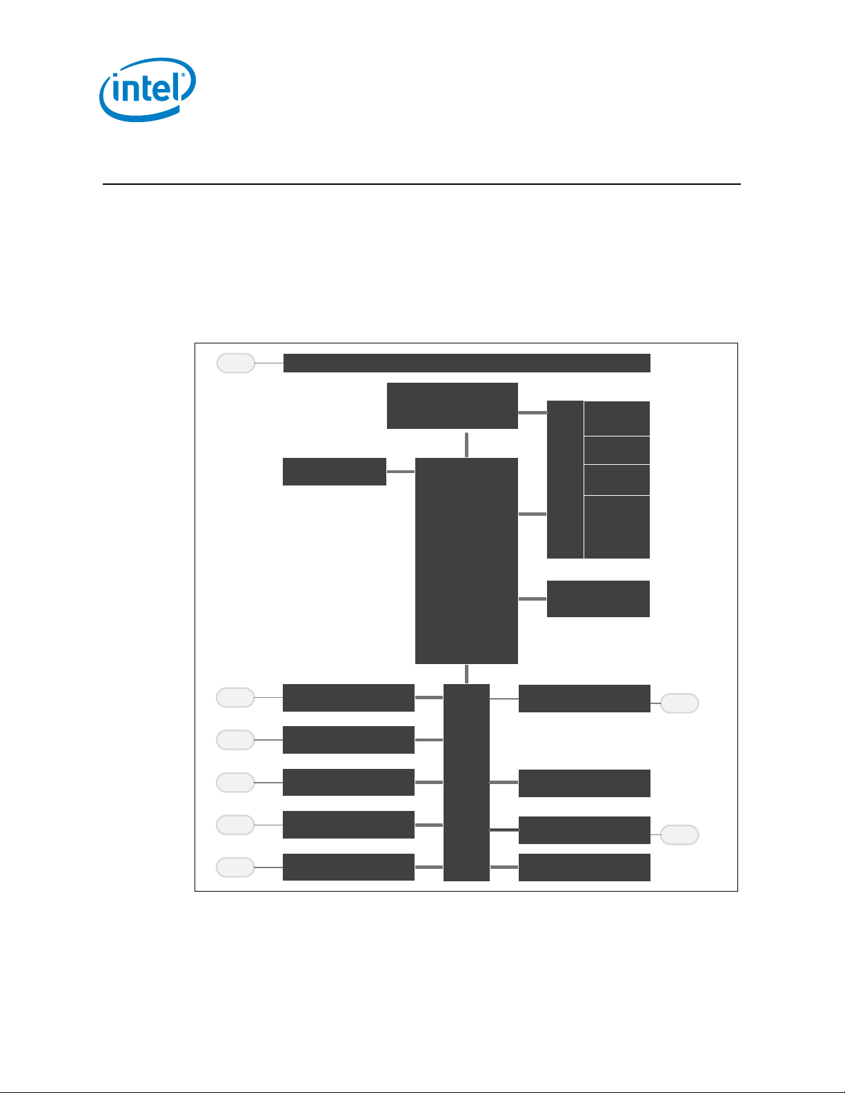
1 Introduction
8KB
SRAM
I2C
I/O
Fabric
Comparators
UART
IO 19
IO 25
IO
1M/S
IO 2
SPI
IO 1M
1S
Quark
TM
Core
SoC
Fabric
Memory
Subsystem
JTAG
32KB
Flash
IO
ADC
IO 19
Internal Clocks
GPIO
Real Time C lo c k
Watchdog Timer
DMA
Controller
8KB
OTP Flash
4KB Dat a
OTP
Timers/PWM
IO 2
The Intel® Quark™ microcontroller D2000 is an ultra-low power Intel Architecture
(IA) SoC that integrates an Intel® Quark processor core, Memory Subsystem with ondie volatile an d non-volatile storage, and I/O interfaces into a single low-cost systemon-chip solution.
Figure 1 shows the system level block diagram of the SoC. Refer to the subsequent
chapters for detailed information on the individual functional blocks.
Figure 1. SoC Block Diagram
Introduction
Intel® Quark™ microcontroller D2000
Datasheet January 2016
16 Document Number: 333577-002EN
Page 17

Introduction
1.1 Feature Overview
1.1.1 Clock Oscillators
• 32 MHz Clock (system clock) generated by on-die Hybrid Oscillator which
works in either:
o Silicon mode (external crystal not needed) (generates 4/8/16/32 MHz
clock output as configured) or
o Crystal mode (external 32MHz crystal required).
• 32.768 kHz RTC Clock generated by on-die RTC Crystal oscillator (external
32.768kHz crystal required). SoC is designed to work without RTC clock, if
there is no use-case for RTC clock.
1.1.2 Quark Processor Core
• 32 MHz Clock Frequency
• 32-bit Address Bus
• Pentium 586 ISA Compatible without x87 Floating Point Unit
• Integrated Local APIC and I/O APIC
• 1 32-bit timer in Local APIC running with system/core clock
1.1.3 Memory Subsystem
• 32 KB of 64b wide on-die Flash
• Supports Page Erase and Program cycles
• Supports configurable wait states to allow Flash to run at various frequencies. At
32MHz, 2-wait-states are introduced for all accesses
• 4 configurable Protection regions for Flash access control
• 8 KB Code OTP with independent read-disable of the two 4KB regions
• 4 KB Data OTP (One-time-programmable) memory
• 8 KB of on-die SRAM with 64b interface with 0-wait state in case of no arbitration
conflict
• 4 configurable Protection regions for SRAM access control
1.1.4 I2C
• One I2C Interface
• Three I2C speeds supported : Standard Mode (100 Kbps), Fast Mode (400 Kbps)
and Fast Mode Plus (1 Mbps)
• 7-bit and 10-bit Addressing Modes Suppo rted
• Supports Master or Slave operation
• FIFO mode support (16B TX and RX FIFO’s)
• Supports HW DMA with configurable FIFO thresholds
1.1.5 UART
• Two 16550 compliant UART interfaces
• Supports baud rates from 300 to 2M with less than 2% frequency error
• Support for hardware and software flow control
• FIFO mode support (16B TX and RX FIFO’s)
January 2016 Datasheet
Document Number: 333577-002EN 17
Intel® Quark™ microcontroller D2000
Page 18

• Supports HW DMA with configurable FIFO thresholds
• Supports 9-bit serial operation mode
• Supports RS485
• Support for DTR/DCD/DSR/RI Modem Control Pins through GPIO pins controlled
by Software
1.1.6 SPI
• One SPI Master Interfaces with support for SPI clock frequencies up to 16 MHz
• One SPI Slave Interface with support for SPI clock frequencies up to 3.2 MHz
• Support for 4-bit up to 32-bit Frame Size
• Up to four Slave Select pins per Master interface
• FIFO mode support (Independent 32B TX and RX FIFO’s)
• Supports HW DMA with configurable FIFO thresholds
1.1.7 DMA Controller
• Provides 2 Unidirectional Channels
• Provides support for 16 HW Handshake Interfaces
o tx and rx channels of I
controller, two UART controllers use this interface
• Supports Memory to Memory, Peripheral to Memory, Memory to Peripheral and
Peripheral to Peripheral transfers
• Dedicated Hardware Handshaking interfaces with peripherals plus Software
Handshaking Support
• Supports Single and Multi-Block Transfers
Introduction
2
C controller, SPI Slave controller, SPI Master
1.1.8 GPIO Controller
• Provides 25 independently configurable GPIO
• All GPIOs are interrupt capable supporting level sensitive and edge triggered
modes
• Debounce logic for interrupt source
• All 25 GPIOs are Always-on interrupt and wake capable
1.1.9 Timers
• Two 32-bit Timers running at system clock (running in timer mode or PWM mode)
• Supports an additional 32-bit Always-On Counter running with 32.768 kHz clock
• Supports an additional 32-bit Always-On Periodic Timer running with 32.768 kHz
clock and with interrupt and wake capability
1.1.10 Pulse Width Modulation (PWM)
• Two 32-bit Timers running at system clock can be configured to generate two
PWM outputs
Intel® Quark™ microcontroller D2000
Datasheet January 2016
18 Document Number: 333577-002EN
Page 19

Introduction
1.1.11 Watchdog Timer
• Configurable Watchdog timer with support to trigger an interrupt and/or a system
reset upon timeout
1.1.12 Real Time Clock (RTC)
• 32-bit Counter running from 1Hz up to 32.768 kHz
• Supports interrupt and wake event generation upon match of programmed value
• Only requires 32.768 kHz clock to be running to generate interr u pt a n d w ake
events
1.1.13 Analog to Digital Convertor (ADC)
• 19 Analog Input channels
• Selectable 6/8/10/12-bit resolution
• Supports maximum of 2.28 Mega Samples Per Second (MSps) at 12-bit resolution
and 4 MSps at 6-bit resolution)
• Differential Non-Linearity DNL of +/- 1.0 LSB
• Integral Non-Linearity INL of +/- 2.0 LSB
• SINAD of 68 dBFS
• Offset Error of +/- 2 LSB (calibration enabled), +/- 64 LSB (calibration disabled)
• Full-scale input range of 0 to AVDD.
1.1.14 Analog Comparators
• Provides 19 Analog Comparators
• Six high performance comparators
• 13 low power comparators
• Configurable polarity
• Interrupt and Wake Event capable
1.1.15 Interrupt Routing
• Configurable Routing of SoC Interrupts with capability to route to the Interrupt
Controller of the Quark Processor.
• SoC events can be routed as: Interrupts to the Quark Processor, debug break
events to the Quark Processor or SoC Warm Reset requests.
January 2016 Datasheet
Document Number: 333577-002EN 19
Intel® Quark™ microcontroller D2000
Page 20
1.1.16 Power Management
• SoC System States : RUN, Low Power Compute, HALT, Low Power Wait, Deep
Sleep (RTC or NORTC) state.
• Processor States : C0 – C2
• Supports Coin-cell Battery source (2.0V to 3.6V range)
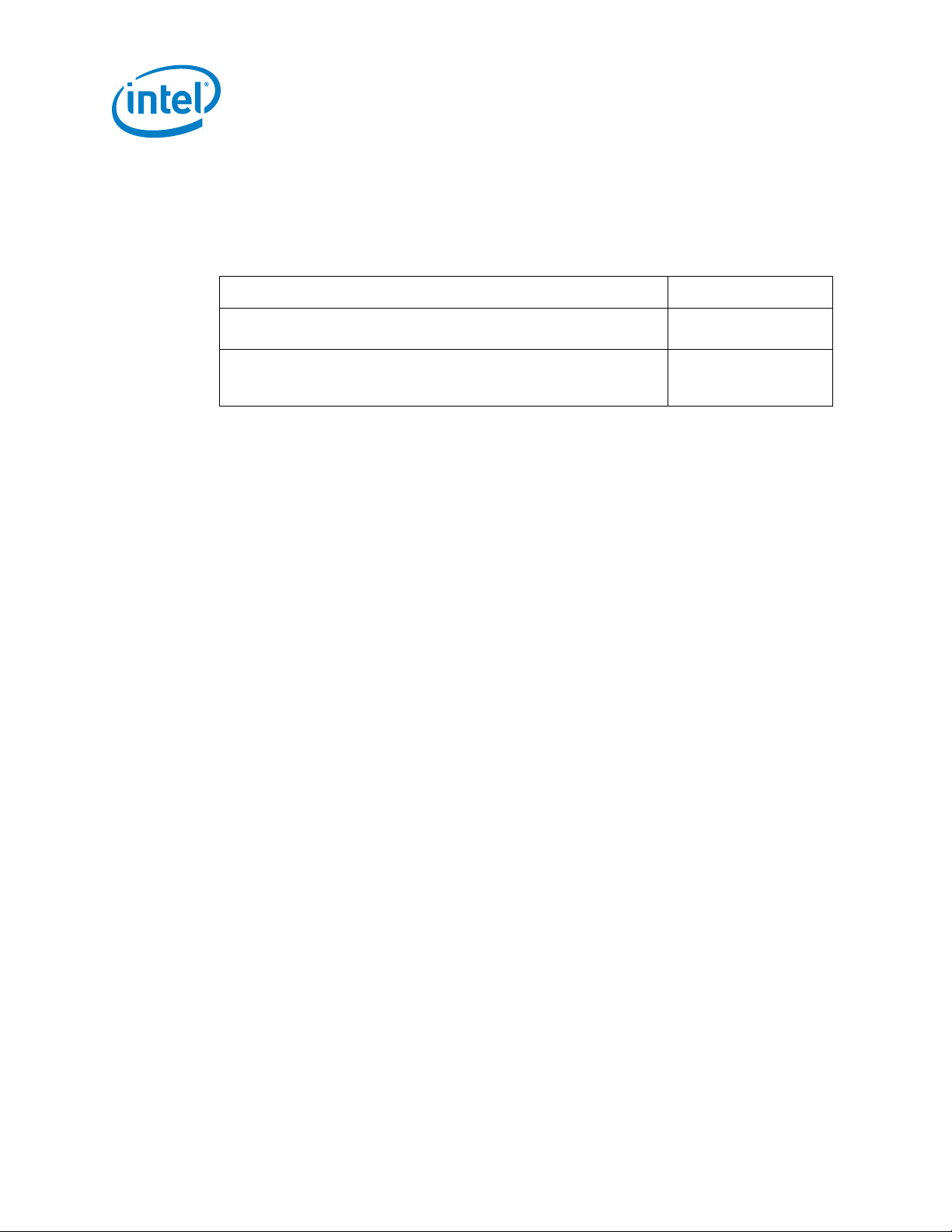
Scenario Max Current Draw
Introduction
Active/RUN state: All SoC components including ADC, Comparators,
clock oscillators, peripheral enabled and core running at 32MHz
Idle/Sleep state: Most SoC components such as ADC, hybrid
oscillator, RTC oscil la tor, peripherals are powered down or clock
gated. Core halted. Only 1 low power-comparator enabled for wake.
1.1.17 Package
40-pin Quad Flat No-Leads (QFN) package.
< 30 mA
< 3.5 µA
§
Intel® Quark™ microcontroller D2000
Datasheet January 2016
20 Document Number: 333577-002EN
Page 21

VSS
Ground
QFN package ground plane
comparators.
isolated version of PVDD.
Physical Interfaces
2 Physical Interfaces
2.1 Pin States Through Reset
All functional IOs will come up in input mode after reset except JTAG TDO output
which is kept tristated.
All Digital IO include a configurable pullup (49K ohm typ; 34K-74Kohm range) with
pull-up disabled by default, except for F_20, F_22, F_23 pins (TRST_N, TMS, TDI))
where pull-up is enabled by default.
The state of all IOs is retained whenever SoC goes into low power states.
2.2 External Interface Signals
The following table gives the definition of external interface signals of Intel® Quark™
microcontroller D2000. Not all interfaces are available simultaneously through
external pins of Intel
refer to Chapter 3
®
Quark™ microcontroller D2000. For pin multiplexing options,
.
Table 1. List of User Mode External Interfa ce s
Interface Pin Name Type Description
Power
PVDD Supply 2.0-3.6 V unregulated battery
supply rail input (can lower to
1.8V if analog comparators are
not used). This rail is used only
by internal voltage regulator.
There is a mechanism to
disable internal voltage
regulator and feed
IOVDD/AVDD/DVDD by
platform directly. PVDD is to be
supplied even if Internal voltage
regulator is not enabled as
internal VR is used to generate
internal voltage reference for
AVDD Supply 2.0-3.6V Analog Voltage Rail
Input powering both ADC and
Comparator - ADC supports
1.8V to 3.3V range, but
Comparator only supports 2V to
3.3V. AVDD can be an AC
January 2016 Datasheet
Document Number: 333577-002EN 21
Intel® Quark™ microcontroller D2000
Page 22
Physical Interfaces
required.
side of inductor.
GSENSE
Analog input
core power ground sense
LX
Supply
Core voltage regulator output
becomes stable.
sleep/leakage power.
reduce sleep/leakage power.
pins as no-connect.
no-connect.
has to be grounded (to 0).
Interface Pin Name Type Description
IOVDD Supply Analog (Driver) side Voltage
Rail Input for IO ring (1.8V to
3.3V Nominal +/- 10%). All
digital IO pads use IOVDD only.
IOVDD can be an AC isolated
version of PVDD but is not
VSENSE Analog input Voltage Regulator Voltage
Sense Input - Feedback of Load
VREN Analog input Internal Voltage regulator
enable:
PVDD = enable
VSS/GND = disable
VREN cannot be dynamically
changed. VREN has to be
stable/static when PVDD
DVDD Supply 1.8 V (nominal) +/- 10%
regulated core power supply. In
Deep Sleep state, it can be
configured to go to 1.35V
(nominal) +/- 10% to reduce
DVDD_2 Supply 1.8 V (nominal) +/- 10%
regulated core power supply.
Connected to same source as
DVDD pin. In Deep Sleep state,
it can be configured to go to
1.35V (nominal) +/- 10% to
Clocking HYB_XTALI Logic input Crystal / oscillator input for
System Clock. If no external
XTAL is connected, keep these
HYB_XTALO Logic output Crystal output for System clock.
If no external XTAL is
connected, keep these pins as
RTC_XTALI Logic input 32.768 kHz Crystal/oscillator
input for RTC clock. If RTC
XTAL is not connected, this pin
Intel® Quark™ microcontroller D2000
Datasheet January 2016
22 Document Number: 333577-002EN
Page 23
0).
32MHz system clock output
RTC_CLK_OUT
Logic Output
32.768 kHz RTC clock output
voltage level.
GPIO
GPIO[24:0]
Logic I/O
General purpose I/O
I2C_SCL
Logic I/O
Open drain clock
I2C_SDA
Logic I/O
Open drain data
PWM1
Logic Output
PWM Output 1
PWM0
Logic Output
PWM Output 0
is outside SoC.
receiver is outside SoC.
(RS232)
UART_A_CTS
Logic input
UART A Clear to send (RS232)
onto UART_A_RTS pin
Physical Interfaces
Interface Pin Name Type Description
Reset RST_N Analog input Active Low reset input with
RTC_XTALO Logic output Crystal output for RTC clock. If
RTC XTAL is not connected,
this pin has to be grounded (to
SYS_CLK_OUT Logic Output Divided (1:1, 1:2, 1:4) version of
Hysteresis. Tie to PVDD for
internal power-on reset.
<0.788V = reset
>1.112V = not reset
RST_N is connected to an
internal comparator which
compares RST_N voltage level
to an internal reference to
assert/deassert internal SOC
reset. There is an internal
mechanism to assert reset if
PVDD is power recycled (power
on reset) irrespective of RST_N
I2C
PWM
UART
UART_A_TXD Logic output UART A single-ended Transmit
data (RS232 or RS485). In
RS485 mode, differential driver
UART_A_RXD Logic input UART A single-ended Receive
data (RS232 or RS485). In
RS485 mode, differential
UART_A_RTS Logic output UART A Request to send
UART_A_DE Logic Output UART A Driver Enable (RS485
mode). Used to control the
differential driver of RS485 in
platform/board. Polarity is
configurable. This is multiplexed
January 2016 Datasheet
Document Number: 333577-002EN 23
Intel® Quark™ microcontroller D2000
Page 24
Physical Interfaces
depending on RS485 or RS232
mode of operation.
RS232 mode of operation.
is outside SoC.
receiver is outside SoC.
(RS232)
UART_B_CTS
Logic input
UART B Clear to send (RS232)
RS232 mode of operation.
SPI_S_SCLK
Logic input
Slave SPI Clock
SPI_S_SDIN
Logic input
Slave SPI Receive data
SPI_S_SCS
Logic input
Slave SPI Slave Chip Select
SPI_S_SDOUT
Logic output
Slave SPI Transmit data
SPI_M_SCLK
Logic output
Master SPI Clock
SPI_M_TXD
Logic output
Master SPI Transmit data
SPI_M_SS[3:0]
Logic output
Master SPI Slave Selects
SPI_M_RXD
Logic input
Master SPI Receive data
Interface Pin Name Type Description
UART_A_RE Logic Output UART B Receiver Enable
(RS485 mode). Used to control
the differential receiver of
RS485 in platform/board.
Polarity is configurable. This is
multiplexed onto UART_B_CTS
pin depending on RS485 or
UART_B_TXD Logic output UART B single-ended Transmit
data (RS232 or RS485). In
RS485 mode, differential driver
UART_B_RXD Logic input UART B single-ended Receive
data (RS232 or RS485). In
RS485 mode, differential
Slave SPI
UART_B_RTS Logic output UART B Request to send
UART_B_DE Logic Output UART B Driver Enable (RS485
mode). Used to control the
differential driver of RS485 in
platform/board. This is
multiplexed onto UART_B_RTS
pin depending on RS485 or
UART_B_RE Logic Output UART A Receiver Enable
(RS485 mode). Used to control
the differential receiver of
RS485 in platform/board. This
is multiplexed onto
UART_B_CTS pin depending
on RS485 or RS232 mode of
operation.
Intel® Quark™ microcontroller D2000
Datasheet January 2016
24 Document Number: 333577-002EN
Master SPI
Page 25
AI[18:6].
RAR also available).
is enabled by default.
enabled by default.
enabled by default.
TCK
Logic input
TAP clock
TDO
Logic output
TAP data output
Physical Interfaces
Interface Pin Name Type Description
Analog AI[18:0] Analog input Comparator/ADC inputs.
JTAG TRST_N Logic input TAP controller reset. A pull-up
AI[18:0] are connected to both
ADC and comparator inputs.
AI[5:0] are connected to 6 fast
response analog comparators.
AI[18:6] are connected to 13
slow response low power
comparators, Since fast
response comparators are
powered off in low power
states, any analog signal that
shall be capable of waking SoC
is to be connected to one of
AR Analog input Comparator Reference Volt age
Input (internal reference from
TDI Logic input TAP data input. A pull-up is
TMS Logic input TAP mode select. A pull-up is
January 2016 Datasheet
Document Number: 333577-002EN 25
Intel® Quark™ microcontroller D2000
Page 26
2.3 GPIO Multiplexing
Not all interfaces can be active at the same time. To provide flexibility, these shared
interfaces are multiplexed with GPIOs.
Note: All 25 functional IOs come up as Function 0 at boot. JTAG is default enabled (as part
of Function 0) instead of GPIO[23:19]. FW is responsible for enabling proper
configuration later on.
Table 2. Multiplexed Functions
Function0 Function1 Function2
GPIO[3:0] ADC/COMP[3:0] SPI_M (4 IO)
GPIO[5:4] ADC/COMP[5:4] RTC_CLK_OUT,
GPIO[7:6] ADC/COMP[7:6] I2C (2 IO)
GPIO[11:8] ADC/COMP[11:8] SPI_S (4 IO)
GPIO[15:12] ADC/COMP[15:12] UART_A (4 IO)
Physical Interfaces
SYS_CLK_OUT
GPIO[18:16] ADC/COMP[18:16] SPI_M (3 IO)
JTAG (5 IO) GPIO[23:19] UART_B (4 IO), PWM0
GPIO[24] - PWM1
Intel® Quark™ microcontroller D2000
Datasheet January 2016
26 Document Number: 333577-002EN
Page 27

Ballout and Package Information
3 Ballout and Package
Information
The Intel® Quark™ microcontroller D2000 comes in 6 mm x 6 mm Quad Flat No-Leads
(QFN) Package.
3.1 SoC Attri b ute s
• Package parameters: 6 mm X 6 mm (QFN)
• Ball Count: 40
All Units: mm
Tolerances if not specified:
• .X: ± 0.1
• .XX: ± 0.05
• Angles: ± 1.0 degrees
January 2016 Datasheet
Document Number: 333577-002EN 27
Intel® Quark™ microcontroller D2000
Page 28
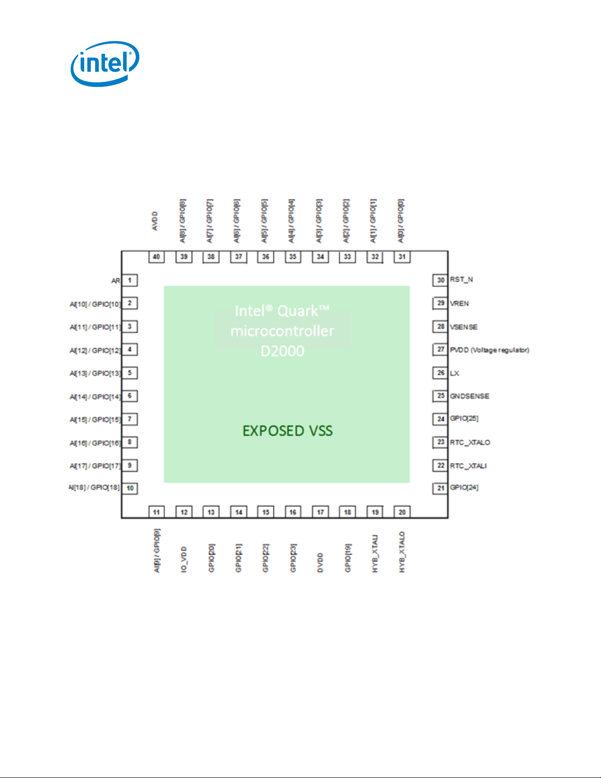
3.2 Package Diagrams
Figure 2. Package Diagram QFN 40 pin (0.5mm pitch)
Ballout and Package Information
Intel® Quark™ microcontroller D2000
Datasheet January 2016
28 Document Number: 333577-002EN
Page 29
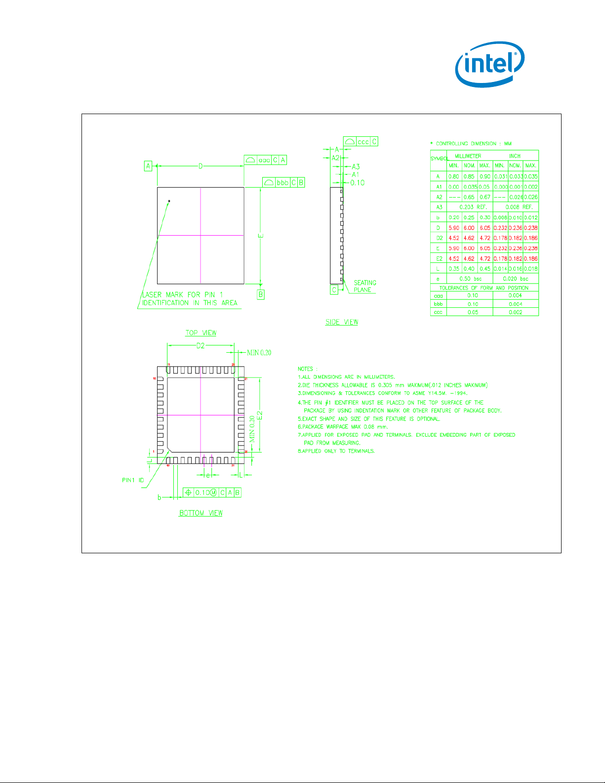
Ballout and Package Information
Figure 3. Mechanical Drawing of Package
January 2016 Datasheet
Document Number: 333577-002EN 29
Intel® Quark™ microcontroller D2000
Page 30
3.3 Pin Multiplexing
VSS
GND
PWR
0 V
GND
GND
GND
GND
27
PVDD
PWR
PVDD
PVDD
PVDD
PVDD
PVDD
40
AVDD
PWR
PVDD
AVDD
AVDD
AVDD
AVDD
12
IOVDD
PWR
PVDD
IOVDD
IOVDD
IOVDD
IOVDD
28
VSENSE
PWR
DVDD
VSENSE
VSENSE
VSENSE
VSENSE
25
GSENSE
PWR
0 V
GSENSE
GSENSE
GSENSE
GSENSE
26
LX
PWR
DVDD
LX
LX
LX
LX
29
VREN
PWR
PVDD
VREN
VREN
VREN
VREN
17
DVDD
PWR
DVDD
DVDD
DVDD
DVDD
DVDD
30
RST_N
RST
PVDD
RST_N
RST_N
RST_N
RST_N
22
RTC_XTALI
CLK
DVDD
RTC_XTALI
RTC_XTALI
RTC_XTALI
RTC_XTALI
23
RTC_XTALO
CLK
DVDD
RTC_XTALO
RTC_XTALO
RTC_XTALO
RTC_XTALO
19
HYB_XTALI
CLK
DVDD
HYB_XTALI
HYB_XTALI
HYB_XTALI
HYB_XTALI
20
HYB_XTALO
CLK
DVDD
HYB_XTALO
HYB_XTALO
HYB_XTALO
HYB_XTALO
1
AR
PWR
AVDD
AR
AR
AR
AR
31
F_0
GPIO
IOVDD/
AVDD
GPIO0
AI0
SPI_M_SS0
32
F_1
GPIO
IOVDD/
AVDD
GPIO1
AI1
SPI_M_SS1
33
F_2
GPIO
IOVDD/
AVDD
GPIO2
AI2
SPI_M_SS2
34
F_3
GPIO
IOVDD/
AVDD
GPIO3
AI3
SPI_M_SS3
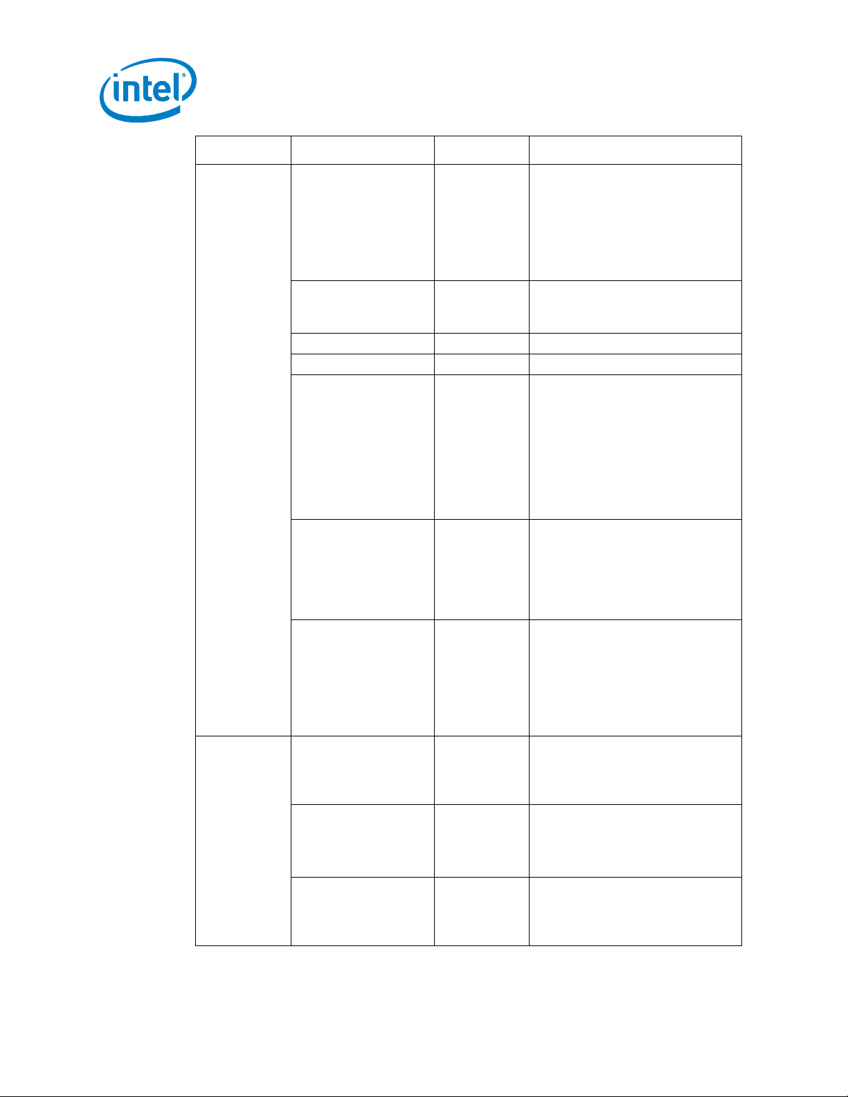
There are 15 dedicated pins + 1 QFN GND plane and 25 functional pins which can be
configured as GPIO (GPIO[24:0]) or other functions (I2C/UART/SPI/JTAG). There are
two major IO modes: user mode and test mode. In user mode, each pin can be
individually configured in one of the 4 user modes (FUNC 0/1/2/3). By default, after
power-on-reset (RST_N) or cold reset, SoC comes up in user mode 0 function
(FUNC0). SOC firmware/software is responsible for enabling the platform specific
configuration by programming the respective IO pad control registers.
Out of 25 functional pins, 19 pins are double bonded to Analog input pads and digital
pads while 6 pins are digital only pads. All analog pads (AI[18:0]) are specified with
respect to AVDD and all digital pads are with respect to IOVDD. The analog inputs (AI)
are connected to ADC or Comparators inside the SoC. AI[5:0] is connected to fast
response/high performance comparator / fast channel of ADC; and AI[18:6] are
connected to slow response/low power comparator / slow channel of ADC. Any wake
capable analog inputs shall be connected only to any of AI[18:6] and not to AI[5:0].
Table 3. Pin Multiplexing
Pin
Num
ber
Pin/Ball
Name Type
Volta
ge
Ballout and Package Information
Function 0 Function 1 Function
2 Function 3
Intel® Quark™ microcontroller D2000
Datasheet January 2016
30 Document Number: 333577-002EN
Page 31

35
F_4
GPIO
IOVDD/
AVDD
GPIO4
AI4
RTC_CLK_O
UT
36
F_5
GPIO
IOVDD/
AVDD
GPIO5
AI5
SYS_CLK_O
UT 37
F_6
GPIO
IOVDD/
AVDD
GPIO6
AI6
I2C_SCL
38
F_7
GPIO
IOVDD/
AVDD
GPIO7
AI7
I2C_SDA
39
F_8
GPIO
IOVDD/
AVDD
GPIO8
AI8
SPI_S_SCLK
11
F_9
GPIO
IOVDD/
AVDD
GPIO9
AI9
SPI_S_SDIN
2 F_10
GPIO
IOVDD/
AVDD
GPIO10
AI10
SPI_S_SDOU
T 3
F_11
GPIO
IOVDD/
AVDD
GPIO11
AI11
SPI_S_SCS
4 F_12
GPIO
IOVDD/
AVDD
GPIO12
AI12
UART_A_TX
D 5
F_13
GPIO
IOVDD/
AVDD
GPIO13
AI13
UART_A_RX
D 6
F_14
GPIO
AVDD
GPIO14
AI14
UART_A_RT
DE 7
F_15
GPIO
AVDD
GPIO15
AI15
UART_A_CT
RE 8
F_16
GPIO
IOVDD/
AVDD
GPIO16
AI16
SPI_M_SCLK
9 F_17
GPIO
IOVDD/
AVDD
GPIO17
AI17
SPI_M_TXD
10
F_18
GPIO
IOVDD/
AVDD
GPIO18
AI18
SPI_M_RXD
-
18
F_19
GPIO
IOVDD
TDO
GPIO19
PWM0
-
13
F_20
GPIO
IOVDD
TRST_N
GPIO20
UART_B_TX
D - 14
F_21
GPIO
IOVDD
TCK
GPIO21
UART_B_RX
D - 15
F_22
GPIO
IOVDD
TMS
GPIO22
UART_B_RT
DE - 16
F_23
GPIO
IOVDD
TDI
GPIO23
UART_B_CT
RE - 21
F_24
GPIO
IOVDD
GPIO24
-
PWM1
-
24
DVDD_2
PWR
DVDD_2
DVDD_2
DVDD_2
DVDD_2
DVDD_2
Ballout and Package Information
Pin
Num
ber
Pin/Ball
Name Type
Volta
ge
IOVDD/
Function 0 Function 1 Function
2 Function 3
S/UART_A_
IOVDD/
S/UART_A_
S/UART_B_
S/UART_B_
All Analog IOs (AI[18:0]/ADC[18:0]) are with respect to AVDD rail.
All Digital IOs are 3.3V tolerant.
January 2016 Datasheet
Document Number: 333577-002EN 31
Intel® Quark™ microcontroller D2000
Page 32

Ballout and Package Information
All Digital IO include configurable drive strength namely low-drive (12 mA) and highdrive (16 mA) modes. By default, all digital IOs come up in low-drive mode.
All Digital IO include a configurable pullup with pull-up disabled by default , except for
F_20, F_22, F_23 (TRST_N, TMS, TDI)) where pull-up is enabled by default.
UART_A/B_CTS (input) or UART_A/B_RE (output) is available based on UART mode of
operation (RS232 or RS485) configurable in respective UART controller. Similarly for
UART_A/B_RTS (output) or UART_A/B_DE (output). Default is RS232. FW can choose
to enable both input and output direction for CTS/RE pins and hardware will control
the output enable of these pins based on RS232 or RS485 mode of operat ion if these
pins are configured for UART function.
JTAG interface is default enabled (user mode 0) to assist in debug as well as
embedded flash programming.
There is a F_25 pad which is not bonded to any pin. This pad (mapped as pin 25 for
pinmux configuration in System Control Subsystem) shall be configured by FW in
input disabled mode (Input Enable = 0; User mode 3 which makes Output Enable
disabled).
DVDD_2 and DVDD are identical and are to be connected to the same source.
Intel® Quark™ microcontroller D2000
Datasheet January 2016
32 Document Number: 333577-002EN
Page 33

1
AR
PWR
AVDD
AR
AR
AR
AR
D
D
DE
D
RE
D
12
IOVDD
PWR
PVDD
IOVDD
IOVDD
IOVDD
IOVDD
13
F_20
GPIO
IOVDD
TRST_N
GPIO20
UART_B_TXD
-
14
F_21
GPIO
IOVDD
TCK
GPIO21
UART_B_RXD
-
DE
RE
17
DVDD
PWR
DVDD
DVDD
DVDD
DVDD
DVDD
Ballout and Package Information
3.4 Alphabetical Ball Listing
Table 4 shows pins arranged in increasing order of pin number.
Table 4. Pins Listed in increasing Order of Pi n N umber
Pin
Numbe
r
Pin/Ball
Name
Typ
e
Voltage Function 0 Function
1
Function 2 Function
3
2 F_10 GPIO IOVDD/AVD
3 F_11 GPIO IOVDD/AVDD GPIO11 AI11 SPI_S_SCS
4 F_12 GPIO IOVDD/AVD
5 F_13 GPIO IOVDD/AVDD GPIO13 AI13 UART_A_RXD
6 F_14 GPIO IOVDD/AVDD GPIO14 AI14 UART_A_RTS/UART_A_
7 F_15 GPIO IOVDD/AVD
8 F_16 GPIO IOVDD/AVDD GPIO16 AI16 SPI_M_SCLK
9 F_17 GPIO IOVDD/AVD
10 F_18 GPIO IOVDD/AVDD GPIO18 AI18 SPI_M_RXD -
11 F_9 GPIO IOVDD/AVDD GPIO9 AI9 SPI_S_SDIN
GPIO10 AI10 SPI_S_SDOUT
GPIO12 AI12 UART_A_TXD
GPIO15 AI15 UART_A_CTS/UART_A_
GPIO17 AI17 SPI_M_TXD
15 F_22 GPIO IOVDD TMS GPIO22 UART_B_RTS/UART_B_
16 F_23 GPIO IOVDD TDI GPIO23 UART_B_CTS/UART_B_
January 2016 Datasheet
Document Number: 333577-002EN 33
Intel® Quark™ microcontroller D2000
-
-
Page 34

Ballout and Package Information
18
F_19
GPIO
IOVDD
TDO
GPIO19
PWM0
-
HYB_XTALI
HYB_XTALI
HYB_XTALI
O
O
O
21
F_24
GPIO
IOVDD
GPIO24
-
PWM1
-
RTC_XTALI
RTC_XTALI
RTC_XTALI
O
O
O
24
DVDD_2
PWR
DVDD_2
DVDD_2
DVDD_2
DVDD_2
DVDD_2
25
GSENSE
PWR
0 V
GSENSE
GSENSE
GSENSE
GSENSE
26
LX
PWR
DVDD
LX
LX
LX
LX
27
PVDD
PWR
PVDD
PVDD
PVDD
PVDD
PVDD
28
VSENSE
PWR
DVDD
VSENSE
VSENSE
VSENSE
VSENSE
29
VREN
PWR
PVDD
VREN
VREN
VREN
VREN
30
RST_N
RST
PVDD
RST_N
RST_N
RST_N
RST_N
D
D
D
Pin
Numbe
r
19 HYB_XTALI CLK DVDD
20 HYB_XTALO CLK DVDD
22 RTC_XTALI CLK DVDD
23 RTC_XTALO CLK DVDD
Pin/Ball
Name
Typ
e
Voltage Function 0 Function
HYB_XTAL
RTC_XTAL
1
HYB_XTAL
RTC_XTAL
Function 2 Function
HYB_XTALI
HYB_XTALO
RTC_XTALI
RTC_XTALO
3
HYB_XTAL
RTC_XTAL
31 F_0 GPIO IOVDD/AVDD GPIO0 AI0 SPI_M_SS0
32 F_1 GPIO IOVDD/AVD
33 F_2 GPIO IOVDD/AVDD GPIO2 AI2 SPI_M_SS2
34 F_3 GPIO IOVDD/AVD
35 F_4 GPIO IOVDD/AVDD GPIO4 AI4 RTC_CLK_OUT
36 F_5 GPIO IOVDD/AVD
37 F_6 GPIO IOVDD/AVDD GPIO6 AI6 I2C_SCL
GPIO1 AI1 SPI_M_SS1
GPIO3 AI3 SPI_M_SS3
GPIO5 AI5 SYS_CLK_OUT
Intel® Quark™ microcontroller D2000
Datasheet January 2016
34 Document Number: 333577-002EN
Page 35

D
40
AVDD
PWR
PVDD
AVDD
AVDD
AVDD
AVDD
VSS
GND
PWR
0 V
GND
GND
GND
GND
L
Cout
Supply Rail
2.0V – 3.6V
Cin
VREG 1.8V
(200mV dropout)
AVD
VOUT
GNDSE NSE
AVS
LX
VSENSE
EN
VDD_CTR L
PVDD V REN
LX
VSENS E
DVDD
GSEN SE
VSS
VREF_O UT
SoC
Optional
Ballout and Package Information
Pin
Numbe
Pin/Ball
Name
Typ
e
Voltage Function 0 Function
1
Function 2 Function
r
38 F_7 GPIO IOVDD/AVDD GPIO7 AI7 I2C_SDA
39 F_8 GPIO IOVDD/AVD
GPIO8 AI8 SPI_S_SCLK
3.5 Platform Requirements
3.5.1 3.5.1 Internal Voltage Regulator
Figure 4. Internal Voltage Regulator
3
January 2016 Datasheet
Document Number: 333577-002EN 35
Intel® Quark™ microcontroller D2000
Page 36

Ballout and Package Information
Capacitor
Capacitor
Inductor
Maximum total resistance (including wirebond, package pin
must be less than 400mΩ/nb PVDD pads.
Has to be star-connected: no current should flow through
package pin and board routing) must be lower than 100Ω.
The requirement for external component at PCB level is as shown in the table:
Component
Name
Description Characteristic Value Accuracy Unit
Cin Input
Cout Output Tank
L Switching
ESR rating for Cin and Cout:
For Cout: Resr(TYP) = 100mOhm / Resr(MAX) = 500mOhm
For Cin: Resr(TYP ) = 25mOhm / Resr(MAX) = 100mOhm
Please note for Cout, the higher ESR is, the higher the ripple is.
DCR rating for on-board inductor
L: DCR(TYP) = 100mOhm, DCR(MAX) = 500mOhm
The DCR impacts the efficiency of the regulator. The higher the DCR is, the lower the
efficiency is.
Also, the voltage drop across the DCR increases the min dropout the regulator can
support. For example, the minimum dropout specified in the spec is 200mV (Table 11)
by considering a 0.1 Ohm DCR. If the DCR is higher, the dropout will also be higher.
Ceramic 470 +/- 20% nF
Ceramic 4.7 +/- 20% µF
47 +/- 30% µH
For example, DCR=0.5 Ohm = 0.1 + 0.5. For a 50 mA current, the dropout is 20 mV
higher (0.4 Ohm*50mA).
Table 5. Parasitic Requirement for Voltage Regulator Pins
Item Description
PVDD
VSENSE
Intel® Quark™ microcontroller D2000
Datasheet January 2016
36 Document Number: 333577-002EN
and board routing) between PVDD PIN and Input Supply
this path between VSENSE pin and the regulated voltage
node. Access resistance to this port (including wirebond,
Page 37

Maximum total resistance (including wirebond, package pin
should flow through this connection.
Maximum total resistance (including wirebond, package pin
on this PAD.
Maximum total resistance (including wirebond, package pin
VOUT output or any other supply
DVDD
As small as possible
Maximum total resistance (including wirebond, package pin
must be less than 400mΩ/nb LX pins.
Maximum total resistance (including internal wiring parasitic,
less than 20Ω.
Must be placed within 0.2-0.4 inch of IC
Must be placed within 0.2-0.4 inch of IC
Inductance between package gnd plane and board gnd plane
< 1nH
Ballout and Package Information
Item Description
GNDSENSE
and board routing) between GNDSENSE and Ground plane
must be less than 400mΩ. This pin should be star connected
to the reference (GND) of the load circuit. No load current
AVS
VDD_CTRL
LX
VOUT
and board routing) between AVS and Ground plane must be
less than 400mΩ/nb AVS pads. No other connections allowed
and board routing) between VDD_CTRL pin and Input Supply
must be less than 20Ω. May be tied to VREG external node,
and board routing) between LX PIN and package Input Pin
wirebond, package pin and board routing) between VREG pin
and the regulation point (VSENSE pin connection) must be
CIN
C
out
Package-Board Gnd
When internal voltage regulator is disabled (VR_EN = 0), PVDD must be pow er ed u p,
GNDSENSE and AVS must be grounded. LX is HIZ, VSENSE to be grounded.
3.5.2 RTC Oscillator
For 32.768 kHz RTC Oscillator, refer to
http://www.murata.com/products/timingdevice/crystalu/technical/notice for PCB
guidelines.
Load capacitor on XTAL pins are integrated inside the chip but they are not adjustable.
A nominal value of 11 pF is on each pin (range: 6 pF minimum and 17 pF maximum).
If there is no RTC Oscillator need, then a platform need not mount RTC XTAL on board
and keep RTC_XTAL1, RTC_XTAL0 pins grounded.
January 2016 Datasheet
Document Number: 333577-002EN 37
Intel® Quark™ microcontroller D2000
Page 38

3.5.3 Hybrid Oscillator
Hybrid oscillator can work in internal Silicon RC oscillator mode with +/- 2% accuracy
(after trimming). If a system does not require higher accuracy system clock, then
HYBOSC 32MHz XTAL need not be mounted on board to save cost and in such case,
keep HYB_XTAL1, HYB_XTAL0 pins as no-connect (floating).
A programmable capacitive load can be added on the crystal terminals internal to the
chip to fine tune the crystal frequency. The range and step size will vary depending on
external load, process corners and crystal parameters. Load capacitance is adjustable
through SCSS register in SoC (OSC0_CFG1.OSC0_FADJ_XTAL[3:0] register – range
supported is 5.55 pF to 15.03 pF with default value of 10pF).
Ballout and Package Information
Intel® Quark™ microcontroller D2000
Datasheet January 2016
38 Document Number: 333577-002EN
Page 39

Ballout and Package Information
3.5.4 ADC
A simple filter is recommended to be put on board on Analog Inputs [19:0] connected
to ADC, to reduce external noise. It should be understood that any additional
frequency signals within the band of interest will be present in the output spectrum
contributing for a performance impact. Additionally the input signal is disturbed by the
fast transients due to the fast charging of the ADC input capacitor during the start of
the sampling period. These transients should vanish quite rapidly and the voltage
across the ADC input capacitance should reach a steady state very fast. Nevertheless
in case the ADC input network is not correctly terminated these transients can travel
back and forth through the input line between the ADC driver and ADC input
generating a ringing. This will lead to an incorrect sampling of input signal.
A recommended input scheme to prevent this possible consequence can be
• 50 ohm resistor (in ADC side). The resistor level should match the characteristic
impedance of PCB trace;
• 470pF capacitor to ground (in ADC driver side);
In order that they are effective, resistor and capacitor must be connected very close to
each other and placed towards the ADC Analog input (SoC side), as follows:
Power supply decoupling on AVDD rail input shall be done with 1uF || 10 nF
decoupling capacitors. The 10 nF capacitor shall be ceramic (good quality) and must
be placed as close as possible to the SoC.
January 2016 Datasheet
Document Number: 333577-002EN 39
Intel® Quark™ microcontroller D2000
Page 40

Electrical Characteristics
• Used by internal voltage
very low (< 5 µA).
• Can be same source as PVDD
• Current draw is 2 mA max.
• Can be same source as PVDD
less.
Voltage
• Core voltage domain. Only 1
voltage.
4 Electrical Characteristics
4.1 Thermal Specifications
Ambient temperature = -40°c to +85°c.
4.2 Voltage and Current Specifications
4.2.1 Absolute Maximum Ratings
Table 6: Absolute Maximum Voltage Ratings
Symbol Ratings min Max Unit Notes
PVDD Battery
Supply
AVDD Analog
Supply
IOVDD Digital IO
Supply
2.0 3.63 V
2.0 3.63 V
1.62 3.63 V
regulator.
• If internal VR is enabled,
current draw is 55 mA max
(specification limit). Actual
current draw would be less
based on usecase scenario.
• If external VR feeds DVDD,
then current draw on PVDD is
but noise isolated.
• Used by ADC and
Comparators.
but optionally noise isolated.
• Used by 26 IO digital pads.
• Current draw depends on
platform components and
how many digital IO pads are
used.
• Each IO pad can source
14mA/18mA max. So max
current draw by all IO pads =
500 mA. But actual
consumption would be much
DVDD/DVDD_2 Regulated
Intel® Quark™ microcontroller D2000
Datasheet January 2016
40 Document Number: 333577-002EN
Core
1.62 1.98 V
Always-on rail for entire SoC
core. This is regulated
Page 41

• Connected to external VR (if
draw is 50 mA max.
State
• In Deep Sleep Power State,
Fo
Crystal
frequency
32
32
32
MHz
Cesr
Crystal ESR
12.68
14.41
50
Ω
Cm
Crystal Motional
Cap
3.34
3.54
pF
Electrical Characteristics
Symbol Ratings min Max Unit Notes
VREN=0); or to Internal VR
output (if VREN=1)(post LC
circuit on LX output pin; see
HAS Chap08). If external
voltage regulator, current
DVDD/DVDD_2 Retention
1.2 1.43 V
mode
1.35V
during
Deep
Sleep
Power
Refer to Power Management chapter on voltage rail sequencing in internal voltage
regulator mode and external voltage regulator mode.
4.3 Crystal Specifications
For Hybrid oscillator:
there is an option to lower
core voltage to 1.35V
(nominal) +/- 10% to further
reduce sleep/leakage power,
with implication of increased
power state transition
entry/exit latency.
Table 7: 32MHz Crystal Oscillator specification
January 2016 Datasheet
Document Number: 333577-002EN 41
Symbol Parameter Min Typ Max Unit
Intel® Quark™ microcontroller D2000
Page 42

Electrical Characteristics
Co
Crystal Shunt
Cap
0.84
1.5
pF
CL
Crystal Load Cap
10 pF
Ftol
Frequency
Tolerance
-30 30
ppm
Dlev
Drive Level
(25Ω)
10
µW
Output clock
Without crystal
temperature
-2 +2
%
With crystal
-100
100
ppm
With crystal
after trim
-50 80
ppm
Startup time
Si osc mode –
2% accuracy
2
µs
Crystal mode –
accuracy
2000
µS
frequency
KΩ
Motional Cap
Cap
Symbol Parameter Min Typ Max Unit
frequency
accuracy over
PVT
(si osc mode)
after trim done
at typical
before trim
(excluding
crystal
frequency
tolerance)
frequency
setting within
frequency
settling within
100ppm
Table 8: 32kHz Crystal Oscillator specification
Symbol Parameter Min Typ Max Unit
Fo Crystal
32,768 Hz
Cesr Crystal ESR 50 80
Cm Crystal
Co Crystal Shunt
3.7 pF
1.2 pF
Intel® Quark™ microcontroller D2000
Datasheet January 2016
42 Document Number: 333577-002EN
Page 43

Cap
Tolerance
Dlev
Drive Level
1
µW
Voltage
Voltage
Voltage
Voltage
IOL
12mA @ VOL
14.1
22.9
31.8
mA 16mA @ VOL
18.8
30.6
42.4
mA
IOL
12mA @ VOH
20.7
41.9
69.6
mA 16mA @ VOH
28.7
58.2
96.7
mA
Resistor
Point
Point
Electrical Characteristics
Symbol Parameter Min Typ Max Unit
CL Crystal Load
Ftol Frequency
4.4 DC Specifications
4.4.1 IO DC specifications
For IOVDD=3.3V:
Symbol Parameter Min Typ Max Unit
VIL Input Low
VIH Input High
VOL Output Low
7 pF
-20 20 ppm
-0.3 0.8 V
2 3.6 V
0.4 V
VOH Output High
RPU Pull-up
VT Threshold
VT+ Schmitt
Trigger L-> H
Threshold
January 2016 Datasheet
Document Number: 333577-002EN 43
2.4 V
34K 49K 74K Ohm
1.33 1.4 1.47 V
1.53 1.6 1.66 V
Intel® Quark™ microcontroller D2000
Page 44

Electrical Characteristics
Point
Voltage
Voltage
Voltage
Voltage
IOL
12mA @ VOL
5.8
12.1
21.6
mA 16mA @ VOL
7.7
16.2
28.7
mA
IOL
12mA @ VOH
4.7
12.0
24.3
mA 16mA @ VOH
6.6
16.7
33.8
mA
Resistor
Point
Point
Point
Symbol Parameter Min Typ Max Unit
VT- Schmitt
1.13 1.2 1.27 V
Trigger H-> L
Threshold
FOR IOVDD=1.8V:
Symbol Parameter Min Typ Max Unit
VIL Input Low
VIH Input High
VOL Output Low
VOH Output High
-0.3 0.63 V
1.17 3.6 V
0.45 V
1.35 V
RPU Pull-up
VT Threshold
VT+ L-> H
69K 115K 201K Ohm
0.82 0.89 0.93 V
0.99 1.07 1.12 V
Threshold
VT- H-> L
0.62 0.69 0.77 V
Threshold
Intel® Quark™ microcontroller D2000
Datasheet January 2016
44 Document Number: 333577-002EN
Page 45

input range
voltage
voltage
capacitance
Electrical Characteristics
4.4.2 Undershoot Voltage Support
SoC supports a undershoot voltage of 300 mV (VIL min of -0.3V) on its input pins.
4.4.3 ADC IO DC characteristics
Symbol Parameter Min Typ Max Unit
Full-scale
0 3.63 V
VREFP Positive
reference
AGNDREF Negative
reference
ADC_cap Input
sampling
2 AVDD AVDD V
0 0 0.1 V
5 pF
January 2016 Datasheet
Document Number: 333577-002EN 45
Intel® Quark™ microcontroller D2000
Page 46

4.5 System Power Consumption
-40≤T≤850c
-40≤T≤850c
-40≤T≤850c
-40≤T≤850c
-40≤T≤850c
-40≤T≤850c
-40≤T≤850c
The data is preliminary and subject to revision in future.
Scenario Condition Min Typ Max Unit
Electrical Characteristics
Total Active Power
(Pavdd + Ppvdd +
Piovdd) with Internal
VR enabled.
- CPU running
Coremark benchmark
workload
- All peripherals clock
gated
- Hybrid Oscillator and
RTC Oscillator running
- ADC and
Comparators powered
down
Total Standby/Halt
Power (Ppvdd + Pavdd
+ Piovdd) with
Internal VR enabled.
- CPU in C2 power
state (executed HALT
instruction)
- All peripherals clock
gated
- Hybrid Oscillator and
RTC Oscillator running
- ADC and
Comparators powered
down
Vpvdd=Vavdd=Viovdd=3.3V
fCPU = 32 MHz,
Vpvdd=Vavdd=Viovdd=3.3V
fCPU = 16 MHz,
Vpvdd=Vavdd=Viovdd=3.3V
fCPU = 8 MHz,
Vpvdd=Vavdd=Viovdd=3.3V
fCPU = 4 MHz,
Vpvdd=Vavdd=Viovdd=3.3V
fCPU = 32 MHz,
Vpvdd=Vavdd=Viovdd=3.3V
fCPU = 16 MHz,
Vpvdd=Vavdd=Viovdd=3.3V
fCPU = 8 MHz,
- 26.4 mW
16.5
8.3
4.7
- 2.3 mW
1.9
1.2
Vpvdd=Vavdd=Viovdd=3.3V
fCPU = 4 MHz,
0
-40≤T≤85
c
0.9
Intel® Quark™ microcontroller D2000
Datasheet January 2016
46 Document Number: 333577-002EN
Page 47

output)
-40≤T≤850c
output)
-40≤T≤850c
-40≤T≤850c
Electrical Characteristics
Scenario Condition Min Typ Max Unit
Total Deep Sleep RTC
Current (Ipvdd +
Iavdd + Iiovdd) with
AON Periodic Timer
Wake.
- CPU in C2 power
state (executed HALT
instruction)
- All peripherals clock
gated
- Hybrid Oscillator
powered down and
RTC Oscillator running
- ADC and
Comparators powered
down
- Internal Voltage
Regulator enabled in
Linear Regulator mode
(1.8V or 1.35V voltage
Total Deep Sleep
NoRTC Current (Ipvdd
+ Iavdd + Iiovdd)
with Low Power
Comparator Wake.
- CPU in C2 power
state (executed HALT
instruction)
- All peripherals clock
gated
- Hybrid Oscillator and
RTC Oscillator
powered down
- ADC and 18
Comparators powered
down. 1 Low Power
Comparator enabled
for wake.
- Internal Voltage
Regulator enabled in
Linear Regulator mode
(1.8V or 1.35V voltage
Vpvdd=Vavdd=Viovdd=3.3V
Vdvdd = 1.8V,
Vpvdd=Vavdd=Viovdd=3.3V
Vdvdd = 1.35V,
0
-40≤T≤85
c
Vpvdd=Vavdd=Viovdd=3.3V
Vdvdd = 1.8V,
Vpvdd=Vavdd=Viovdd=3.3V
Vdvdd = 1.35V,
0
-40≤T≤85
c
- 3.4 µA
- 2.5 µA
- 2.2 µA
- 1.6 µA
Total Deep Sleep
Vpvdd=Vavdd=Viovdd=3.3V
- 1.9 µA
NoRTC Current (Ipvdd
+ Iavdd + Iiovdd)
Vdvdd = 1.8V,
with GPIO Wake.
January 2016 Datasheet
Document Number: 333577-002EN 47
Intel® Quark™ microcontroller D2000
Page 48

Electrical Characteristics
- CPU in C2 power
output)
SPI Master Clock
SPI_M_SCLK frequency
-
16 MHz (= sysclk / 2).
Output delay for
launch clock edge
0 ns
14 ns
Setup time of SPI_M_RXD
sampling edge
15 ns
-
Scenario Condition Min Typ Max Unit
state (executed HALT
Vpvdd=Vavdd=Viovdd=3.3V
instruction)
- All peripherals clock
gated
- Hybrid Oscillator and
Vdvdd = 1.35V,
0
-40≤T≤85
c
RTC Oscillator
powered down
- ADC and
Comparators powered
down.
- 1 GPIO input
enabled for level
sensitive interrupt
wake
- Internal Voltage
Regulator enabled in
Linear Regulator mode
(1.8V or 1.35V voltage
4.6 AC Specificati ons
4.6.1 SPI Master IO AC characteristics
- 1.3 µA
SPI Master interface consists of:
The interface is timed with respect to SPI_M_SCLK which is output from SoC. A given
signal is launched with respect of a configured edge and sampled with respect to the
opposite edge. Thus it is a half-cycle setup/hold path.
SPI_M_SS[3:0]/SPI_M_TXD
with respect to SPI_M_SCLK
with respect to SPI_M_SCLK
Intel® Quark™ microcontroller D2000
Datasheet January 2016
48 Document Number: 333577-002EN
• Outputs SPI_M_SCLK, SPI_M_TXD, SPI_M_SS[3:0]
• Inputs SPI_M_RXD
Parameter Min Max
Page 49

Hold time of SPI_M_RXD
sampling edge
0 ns
SPI Slave Clock SPI_S_CLK
Frequency
Setup time of
with respect to sampling
edge of SPI_S_SCLK input
Hold time of
with respect to sampling
edge of SPI_S_SCLK input
Output delay of
to launching edge of
SPI_S_SCLK input
Electrical Characteristics
Parameter Min Max
with respect to SPI_M_SCLK
Output load supported for SPI_M_TXD, SPI_M_SS[3:0], SPI_M_SCLK outputs is 25 pF
max to support max rate of 16 Mbps.
4.6.2 SPI Slave IO AC characteristics
SPI Slave interface consists of:
• Outputs SPI_S_SDOUT
• Inputs SPI_S_SCLK, SPI_S_SDIN, SPI_S_SCS
As per SPI protocol, the interface is timed with respect to SPI_S_SCLK which is input
to SoC. A given signal is launched with respect of a configured edge and sampled with
respect to the opposite edge. Thus it is a half-cycle setup/hold path.
Output load supported for SPI_S_SDOUT output is 50 pF max and 5 pF min.
Parameter Min Max
- 3.2 MHz (= 312.5 ns)
SPI_S_SDIN/SPI_S_SCS
SPI_S_SDIN/SPI_S_SCS
SPI_S_SDOUT with respect
- 30 ns
- 120 ns
0 ns 120 ns
4.6.3 I2C Master/Slave IO AC characteristics
I2C interface consists of I2C_SCL and I2C_SDA bidirectional IOs and can operate in
either master or slave mode. It can operate in standard mode (with data rates 0 to 100
Kbps), fast mode (with data rates less than or equal to 400 Kbps) or fast mode plus
(with data rates less than or equal to 1 Mbps). To support fast mode plus, i2c_m0_clk
(= system clock) shall be greater than or equal to 32 MHz.
2
I
C specification dictates timing relationship between I2C_SCL and I2C_SDA to be
met, which will be broadly taken care by the I2C controller using configuration
registers. SoC complies with the timing and load capacitance given in I2C
specification.
January 2016 Datasheet
Document Number: 333577-002EN 49
Intel® Quark™ microcontroller D2000
Page 50

4.6.4 General IO AC characteristics
TCK clock frequency
8 MHz (125 ns)
-
Setup time of TMS, TDI
of TCK
Hold time of TMS, TDI with
respect to rising edge of
TCK
Output data valid delay of
edge of TCK
Output tristate delay of
edge of TCK
Output load supported for all other IO outputs such as GPIO outputs, PWM, UART is
50 pF max and 5 pF min.
UART interface supports maximum baud rate of 2 Mbaud when system clock
frequency is 32 MHz.
All GPIO and PWM outputs will get reflected within 1 system clock period of 30ns on
the output pins.
4.6.5 JTAG Interface AC characteristics
The JTAG interface is a 5-pin interface timed with respect to TCK input clock.
• TMS, TDI are inputs which are sampled by SoC on rising edge of TCK a nd is
expected to be driven by JTAG host on f a l l ing edge of TCK.
• TDO is output from SoC driven on falling edge of TCK and expected to be
sampled by JTAG host on rising edge of TCK.
Electrical Characteristics
• TRSTB is asynchronous signal.
Delays shown in the following table are with respect to SoC.
Parameter Min Max
with respect to rising edge
25 ns -
0 ns -
TDO with respect to falling
TDO with respect to falling
Output load supported for JTAG TDO output is 40 pF max and 5 pF min.
1 ns 40 ns
- 40 ns
Intel® Quark™ microcontroller D2000
Datasheet January 2016
50 Document Number: 333577-002EN
Page 51

Register Access Methods
5 Register Access Methods
All SoC registers are accessed as Fixed Memory Mapped Registers.
The SoC does not contain any of these traditional x86 memory register types: Fixed
IO, IO Referenced, Memory Referenced, PCI Configurati o n o r Messa ge Bu s Registers.
5.1 Fixed Memory Mapped Register Access
Fixed Memory Mapped IO (MMIO) registers are accessed by specifying their 32-bit
address in a memory transaction from the CPU core. This allows direct manipulation of
the registers. Fixed MMIO registers are unmovable registers in memory space.
5.2 Register Field Access Types
Table 9. Register Access Types and Definitions
Access Type Meaning Description
RO Read Only In some cases, if a register is read only, writes to this
register location have no effect. H owever, in other cases,
two separate registers are locate d at the same location
where a read accesses one of the regist ers and a write
accesses the other register. See the I/O and memory map
tables for details.
WO Write Only In some cases, if a register is write only, reads to this
register location have no ef fect. However, in other cases,
two separate registers are locate d at the same location
where a read accesses one of the regist ers and a write
accesses the other register. See the I/O and memory map
tables for details.
R/W Read/Write A register with this attribute can be read and written.
R/WC Read/Write
Clear
R/WO Read/Write-
Once
R/WLO Read/Write,
Lock-Once
/P Sticky A register bit with this attribute is sticky that is it will
Reserved Reserved The value of reserved bits must never be changed.
A register bit with this attribute can be read and written.
However, a write of 1 clears (sets to 0) the corresponding
bit and a write of 0 has no effect.
A register bit with this attribute can b e w ritten only once
after power up. After the first write, the bit becomes read
only.
A register bit with this attribute can be written to the nonlocked value multip le times, but to the locked value only
once. After the locked value has been written, the bit
becomes read only.
retain its state across warm-reset.
January 2016 Datasheet
Document Number: 333577-002EN 51
Intel® Quark™ microcontroller D2000
Page 52

Register Access Methods
Access Type Meaning Description
Default Default When the processor is reset, it sets its registers to
predetermined default states. The default state represents
the minimum functionality feature set required to
successfully bring up the system . Hence, it does not
represent the optimal sy stem configuration. It is the
responsibility of the system initialization software to
determine configuration, operating parameters, and
optional system features that are applicable, and to
program the processor registers accordingly.
Intel® Quark™ microcontroller D2000
Datasheet January 2016
52 Document Number: 333577-002EN
Page 53

Mapping Address Spaces
6 Mapping Address Spaces
The SoC supports a single flat Memory address space. The SoC does not support IO
Address Space, PCI Configuration Space or Message Bus Space.
The Lakemont Processor core (LMT) can directly access memory space either through
code fetches over ITCM or data fetches over DTCM or through memory reads and
writes over AHB fabric.
This chapter describes how memory space is mapped to interfaces and peripherals in
the SoC.
6.1 Physical Address Space Mappings
Processor supports 32b addressing. There are 4 GB (32-bits) of phy sical address
space that can be used as:
• Memory Mapped I/O (MMIO – I/O fabric)
• Physical Memory (System Flash/System SRAM)
The LMT can access the full physical address space. DMA Controller, the only other
master agent on AHB fabric, can only access regions of physical address space allowed
via the multi-layer SoC fabric – see more details under SoC Fabric section.
All SoC peripherals map their registers and memory to physical address space. This
chapter summarizes the possible mappings.
6.1.1 SoC Memory Map
The SoC Memory Map is divided up as follows:
• Processor Local APIC (LAPIC)
• I/O APIC
• SoC Configuration registers
• SoC Peripherals
• System Flash (Flash and ROM – implemented as 2 distinct regions of OTP)
• System SRAM (Internal)
The LMT reset vector at 150h is located in OTP Code region of Intel
microcontroller D2000. System addresses 0xFFFF_FFF0 and 0xFFFF_FFF8 are a special
case by LMT and get aliased to reset vector.
®
Quark™
January 2016 Datasheet
Document Number: 333577-002EN 53
Intel® Quark™ microcontroller D2000
Page 54

Mapping Address Spaces
Table 10 SoC Memory Map
Function Start Address End Address Size
LAPIC 0xFEE0_0000 0xFEE0_0FFF 4KB
IOAPIC 0xFEC0_0000 0xFECF_FFFF 1MB
SCSS (System Control Subsystem) 0xB080_0000 0xB080_3FFF 16KB
DMA 0xB070_0000 0xB070_0FFF 4KB
Internal SRAM Configuration 0xB040_0000 0xB040_03FF 1KB
Flash Configuration 0xB010_0000 0xB010_03FF 1KB
ADC 0xB000_4000 0xB000_43FF 1KB
I2C_0 0xB000_2800 0xB000_2BFF 1KB
UART_B 0xB000_2400 0xB000_27FF 1KB
UART_A 0xB000_2000 0xB000_23FF 1KB
SPI_S 0xB000_1800 0xB000_1BFF 1KB
SPI_M0 0xB000_1000 0xB000_13FF 1KB
GPIO 0xB000_0C00 0xB000_0FFF 1KB
APB Timer 0xB000_0800 0xB000_0BFF 1KB
RTC 0xB000_0400 0xB000_07FF 1KB
Watchdog Timer 0xB000_0000 0xB000_03FF 1KB
SRAM (DTCM & AHB) 0x0028_0000 0x0028_1FFF 8KB
OTP Data (AHB) 0x0020_0000 0x0020_0FFF 4KB
Flash Code (ITCM & AHB) 0x0018_0000 0x0018_7FFF 32KB
OTP Code (ITCM & AHB) 0x0000_0000 0x0000_1FFF 8KB
Notes:
• LMT Reset Vector is located in OTP Code region at address 0x0000_01 50
• All memory regions not covered in the SoC Memory Map are reserved.
Reserved regions are unused. Reserved sections have been insert ed to a llow
space for memory/peripheral address space to increase in derivative SoCs
without re-arranging the address map. Access to Reserved regions trigger an
interrupt to support debug of out of bound accesses. Writes to such regions
have no effect while reads return a definite value dependin g on th e interface.
AHB Fabric provides 4 HSELs to Flash Memory subsystem: Flash CREGs for
configuration, Instruction Flash, OTP Code and OTP Flash Data.
Memory accesses are routed by the IO fabric based on fixed memory ranges that map
to the SoC peripherals. These peripherals are: ADC, I2C, UART*, S PI*, GPIO, APB
Timer, RTC and Watchdog Timer. The fixed regions assigned to each peripheral are
listed in the table above. See the register maps of all peripheral devices for details.
Intel® Quark™ microcontroller D2000
Datasheet January 2016
54 Document Number: 333577-002EN
Page 55

LMT M aster
DMA Contro ller Master
Flash Slave
SRAM Slave
DMA Controller Slave SCSS Slave
APB Pe ripherals S lave
2 Layer ICM
2 Layer ICM 2 Layer ICM
Mapping Address Spaces
LMT clock is gated by HW autonomously based on HALT detection. It is ungated by
HW upon Interrupt assertion. There is an option to gate/ungate clock to Memory
subsystem too with LMT clock. Other than LMT and Memory subsystem clocks, for all
other functions, SW controls gate/ungate of their respective clocks.
6.2 SoC Fabric
The SoC Fabric is a multi-layer AHB fabric that provides interconnect between 2
Masters and 5 Slaves.
The two masters are LMT and DMA Controller – one on each AHB layer. The 5 slaves
are: DMA Controller, Flash, SRAM, SCSS and APB peripherals. The multi-layer fabric
allows multiple masters to access different slaves in parallel. When two or more
masters try to access the same slave simultaneously, the slave arbitrates between the
masters. With this topology, it is not possible for each master to access every slave
connected to the SoC fabric. The LMT master can access all the 5 slaves. DMA
Controller master can only access Flash Slave, SRAM Slave and APB Peripherals Slave.
Figure 5 Multi-Layer AHB fabric with ICM
From an address decode perspective, DMA controller can target all destinations inside
Flash subsystem (Flash Configuration registers, Instruction Flash, 8KB OTP, 4KB OTP)
and all destinations inside SRAM subsystem (SRAM and SRAM Configuration
registers).
The Multi-layer AHB fabric also makes use of the HMASTER port on two ICM
components ICM_SRAM and ICM_FLASH. The HMASTER port on these two ICMs is
used by the slave for memory protection of the SRAM and Flash slaves. Each
HMASTER port for each layer on the ICM has a different ID code, this allows the slave
to identify which master is currently trying to access memory.
January 2016 Datasheet
Document Number: 333577-002EN 55
Intel® Quark™ microcontroller D2000
Page 56

LMT 0x1 DMA
0x4
Table 11 Multi-Layer AHB Fabric Master ID List
AHB Master ID Codes
AHB Master ID Code
Mapping Address Spaces
APB Fabric has 10 slaves – GPIO, I2C Master/Slave, SPI Master, SPI Slave, 2 UARTs,
ADC, RTC, WDT and Timers block. Even though DMA engine can perform concurrent
transfers, single outstanding transaction limitation of AHB prevents simultaneous
transfers to/from multiple peripherals.
Intel® Quark™ microcontroller D2000
Datasheet January 2016
56 Document Number: 333577-002EN
Page 57

HYB_XTALI
Clocking
7 Clocking
The Intel® Quark™ microcontroller D2000 clocking is controlled by the Clock Control
Unit (CCU). There are 2 primary clocks in Intel® Quark™ microcontroller D2000, a
System clock and an RTC clock. The sources and frequencies of the primary clocks
are described in subsequent sections. The CCU uses the primary clocks to generate
secondary clocks to sub modules in the SoC. The secondary clocks are gated and
scaled versions of the primary clocks.
7.1 Signal Descriptions
Table 12 provides the dependency on external signals/pins on clockin g. Change from
Atlas Peak is that there is no need to output system clock and RTC clock to platform.
Table 12. External Signals
External Crystal Interface
HYB_XTALO I/O XTAL input
RTC_XTALI I/O RTC XTAL input
RTC_XTALO I/O RTC XTAL input
SYS_CLK_OUT O Divided 32 MHz System Clock
RTC_CLK_OUT O 32 kHz RTC clock output (pin
7.2 Features
The CCU supports the following features:
- Supply of 32.768kHz RTC clock from internal crystal oscillator
- Supply of system clock from:
o an internal hybrid oscillator which can work in either 4/8/16/32 MHz
o an external clock source (through HYB_XTALI input pin)
o 32.768kHz RTC clock (internal muxing)
- Perform clock gating on all output clocks
- Perform clock scaling on all output clocks
Signal Name Direction/
Type
I/O XTAL input or External system
clock
output (pin multiplexed onto
pin F_5 and not dedicated)
multiplexed onto pin F_4 and
not dedicated)
Description
Silicon RC oscillator mode (+/- 2% clock accuracy) or 20-32 MHz
Crystal oscillator mode (+/- 100 ppm clock accuracy; depending on
crystal connected)
January 2016 Datasheet
Document Number: 333577-002EN 57
Intel® Quark™ microcontroller D2000
Page 58

- In “Low Power Compute” state of SoC, hybrid oscillator can be scaled down to
4 MHz with prescaler of 32 to get 125 kHz; or 32.768kHz (RTC clock wherein
hybrid oscillator can be powered down).
In a minimalistic system configuration that does not require RTC clock or strict clock
accuracy (< 100ppm) of system clock, such platforms can choose not to mount
32.768kHz XTAL and/or not to mount 32MHz XTAL and choose to work with 32MHz
Silicon RC oscillator mode of hybrid oscillator. Intel
designed to work with system clock only and does not mandate 32.768kHz RTC clock
for power state transitions, if system/platform does not require RTC clock for its
usecases.
7.2.1 System Clock - Hybrid Oscillator
When the system clock is sourced internally, a Cosmic Circuits hybrid oscillator [1] is
used to generate the clock. The hybrid oscillator can be run in two modes, crystal or
silicon mode depending on the frequency accuracy and current consumption
requirements of the SoC. The hybrid oscillator contains the follow features:
• Crystal mode
o Generates 20-33 MHz clock
o +/-100ppm (dependent on crystal frequency tolerance)
o 2ms start-up time to reach +/-100ppm accuracy
• Silicon mode (default power up mode)
o Generates 4/8/16/32 MHz clock
o One time 10-bit factory trim
o +/-20,000ppm (after process trim)
o Temperature compensation block to limit frequency variation
o 2us start-up time to reach +/-20,000ppm accuracy
• 4mA @ 32MHz in crystal mode [silicon characterization at ~650 uA @ 32 MHz]
• 450uA @ 32 MHz in silicon mode
• 300nA power down leakage current
• Operates with a supply range of 1.62-1.98V
• Outputs a rail-to-rail swing of 1.62-1.98V
• Power down mode to reduce power consumption within the SoC
• Glitch free mux for switching between hybrid and crystal oscillator clocks
• Bypass mode allows an external clock (fed through HYB_XTALI pin) to be
provided through the hybrid oscillator. HYBOSC has to be configured in Crystal
bypass mode (OSC0_EN_CRYSTAL=1, OSC0_EN_MOD E _SEL=1,
OSC0_BYP_XTAL=1)
•
Clocking
®
Quark™ microcontroller D2000 is
7.2.2 RTC Oscillator
A Silicon Gate Oscillator [2] is used to generate a 32.768kHz RTC clock. The RTC
oscillator has the following features:
• Voltage operating range of 1.08-1.98V
• Accuracy of +/-20ppm
• Nominal current consumption of 150nA
• Power down mode consumption of 100nA [TBC]
Intel® Quark™ microcontroller D2000
Datasheet January 2016
58 Document Number: 333577-002EN
Page 59

Clocking
• Bypass mode allows an external clock (fed through RTC_XTALI pin) to be
provided through the RTC oscillator. To achiev e th is, OSC1_BYP_XTAL_UP=1
and OSC1_PD=0)
• 600mS start-up time to reach +/-20ppm
The Intel
®
Quark™ microcontroller D2000 is designed to operate without RTC clock as
well, if platform does not require RTC clock. RTC clock is needed for any of the
following reasons:
• Periodic waking in low power sleep state.
• Real Time Clock
• GPIO based wake (input debouncing/filter)
If above reasons are not required in a platform, then RTC oscillator can be disabled
without connecting RTC XTAL on board. In this mode, only comparator based wake
can be enabled to exit low power state.
7.2.3 Root Clock Frequency Scaling
The Intel® Quark™ microcontroller D2000 supports a single root clock with multiple
supported root clock frequencies
1) 32MHz high accuracy Crystal Oscillator – required for high accuracy
applications.
2) 4/8/16/32MHz silicon Oscillator – A lower power operating mode used by
applications that do not require a high frequency accuracy.
3) 32.768 kHz - entire SoC can operate out of 32.768 kHz clock as system clock
(controlled by CCU_SYS_CLK_SEL register in SCSS) without enabling Hybrid
Oscillator for such applications that require ultra low power without much
compute performance.
7.2.4 Frequency Scaling
The Intel® Quark™ microcontroller D2000 supports a wide range of frequency scaling
options to optimize power.
1) The root system clock frequency can be scaled to 4/8/16/32MHz
2) The Leaf peripheral clock can be independently scaled @ /2 /4 /8 divisions
To apply a DFS setting the following procedure should be followed
1) Apply the clock divider value CCU_XXX_CLK_DIV
2) Apply the clock divider writing ‘0’ CCU_XXX_CLK_DIV_EN
3) Apply the clock divider writing ‘1’ CCU_XXX_CLK_DIV_EN
7.2.4.1 Peripheral DFS requirements
When using DFS it is the responsibility of firmware to adjust any settings in
peripheral/timers to account for the frequency change. Example to achieve a UART
baud rate of 115200 requires a different baud rate divider dependi ng on the
frequency.
January 2016 Datasheet
Document Number: 333577-002EN 59
Intel® Quark™ microcontroller D2000
Page 60

7.2.4.2 Flash DFS requirements
When using DFS on the root fabric clock the flash wait states must be adjusted for
both Flash instances. Refer to Memory Subsystem chapter for further details.
7.2.5 Dynamic Clock Gating
The Intel® Quark™ microcontroller D2000 supports a wide range of clock gating
options
1) Each leaf clock can be dynamically gated by firmware
To apply a DCG the following procedure should be used.
1) Write ‘0’ to the clock gate register CCU_XXX_PCLK_EN
2) The following hardware clock gating options are supported
a. UART low power autonomous hardware clock gating
b. SPI l o w pow er autonomous hardw are clock gating
7.2.5.1 UART autonomous clock gating (ACG)
Clocking
Both UART controllers support ACG mode (CCU_UARTX_PCLK_EN_SW=0). ACG is
asserted when the following occurs
1) Transmit and receive pipeline is clear (no data in the RBR/THR or TX/RX FIFO)
2) No activity has occurred on the SIN/SOUT lines
3) Modem input signals have not changed in more than one character time.
7.2.5.2 SPI autonomous clock gating (ACG)
All SPI controllers support ACG mode (CCU_SPI_XX_PCLK_EN_SW=0). ACG occurs
when the SSIENR register has been written to 0.
Intel® Quark™ microcontroller D2000
Datasheet January 2016
60 Document Number: 333577-002EN
Page 61

Power Management
8 Power Management
This chapter provides information on the power management and power architecture
of the SoC.
Power architecture of SoC is based on the following premise:
1. There is no requirement to supply regulated voltage (1.8v or 3.3v) to platform
components from SoC.
a. This dictates the max current specification of internal voltage regulator
in the SoC.
2. Platform Components and SoC w oul d operate from same battery sou rce (eg
coincell).
a. The IOs of SoC and the Analog components would be on the same rail
as input battery source. Thus the electrical characteristics of SoC IOs
(digital or analog) would be a function of battery rail and not regulated
1.8v/3.3v.
3. SoC has to generate a regulated 1.8v supply (DVDD) from battery i n put fo r
operating its core logic.
a. There is level shifter in IOs between core voltage rail and IO rail
(IOVDD). Similarly analog components such as ADC and Comparators
take care of shifting from analog rail (AVDD) to core/digital rail or
vice-versa.
SoC has 4 power input pins:
1. PVDD – Used by internal voltage regulator only.
2. IOVDD – Used by digital IO pads. Electrical characteristics of all external
digital pins will be with respect to IOVDD.
3. AVDD – Used by Analog components such as ADC and Comparators. Electrical
characteristics of all external analog pins will be with respect to AVDD.
4. DVDD – Used as SoC Core Voltage. Normal mode operating point is 1.8V. It
can be fed either by internal voltage regulator’s output (to be circled back in
board); or from another regulated power supply from platform if internal
voltage regulator is disabled. All of SoC internals will operate with DVDD.
PVDD, IOVDD, AVDD can be from the same power source with noise isolation, or can
be independently supplied.
Power management of SoC is a function of how the individual component/device
power state is managed. The various components in SoC that play a role in power
management are Voltage Regulator, 32 MHz Oscillator, 32 kHz Oscillator, ADC, Analog
Comparators, memories (SRAM, Flash), Processor Core, Peripheral controllers (digital
logic) and IOs. Hence this chapter begins with a discussion on component power
states and then moves on to create System power states based on component power
states. The System power states are defined based on current draw requirement and
latencies involved in entering or exiting a given power state. System power state is
managed in Firmware/Software and not in hardware.
January 2016 Datasheet
Document Number: 333577-002EN 61
Intel® Quark™ microcontroller D2000
Page 62

8.1 Component Power S tates
8.1.1 Voltage Regulator
Table 13. VR Power States
Power Management
Power
State
NRML-1.8V Normal mode. Voltage
RET-1.8V Retention mode. Voltage
RET-1.35V Retention mode. Voltage
OFF HiZ mode. Voltage regulator
regulator (Retention
Alternating Regulator)
functions in switching
regulator (eSR) mode and
able to output 50 mA current.
eSR output regulates. iLR -RET
output set to high impedance.
EN=H, VREGSEL=L. Change
in power state incurs tSTRB of
1 usec + tROK_PROG (T BD).
regulator (Retention
Alternating Regulator)
functions in linear regulator
(iLR) mode and able to output
300 uA current. iLR-RET
output regulates. eSR output
set to high impedance. EN=H,
VREGSEL=H. Change in
power state incurs tSTRB of 1
usec + tROK_PROG (TBD) of
latency.
regulator (Retention
Alternating Regulator)
functions in linear regulator
(iLR) mode and able to output
300 uA current. iLR-RET
output regulates. eSR output
set to high impedance. EN=H,
VREGSEL=H.
is disabled. iLR-RET output is
set to high impedance. eSR
output is set to high
impedance. VREF_OUT is is
set to its nominal value.
EN=L, VREGSEL=x.
Definition Max
Current
90%
efficiency
1% of
current
load
1% of
current
load
- - - Pla t form pulling
Entry
Latency
2 us 20 us writing into
20 us 2 us writing into
3 us 4 us w rit in g in t o
Exit
Latency
How Triggered
AON_VR.VREG_SEL
AON_VR.VREG_SEL
AON_VR.VSEL and
AON_VR.VSTRB
down VR_EN input
pin (use external
voltage regulator)
Note: Silicon OSC minimum current is ~200uA when configured for 4MHz operation (lowest
power mode) – configuring the Voltage Regulator into Low Power is only be supported when
clocking off either 32.768 kHz OSC or 4 MHz Silicon oscillator mode with prescaler set for 125
kHz or lower output.
Intel® Quark™ microcontroller D2000
Datasheet January 2016
62 Document Number: 333577-002EN
Page 63

Power Management
“OFF” power state is entered only when internal regulator is disabled using VREN=L
input pin and 1.8v rail (DVDD input) is fed directly from platform.
Voltage regulator in eSR mode has 90% efficiency down to 0.2 Imax (1 mA) and 70%
efficiency down to 0.01 Imax (500 uA). In iLR mode, power consumpt ion of VR is
about 1% of delivered current.
The SoC power delivery is described in detail in the Power Architecture section.
8.1.2 CPU
Table 14. CPU Power States
Power
State
C0 Active State
C2 Stop Clock / Halt
Definition Max
Processor executing
code
State
Entered via HLT
instruction
Exited via Interrupt
or Reset
Clock to LMT core
including Local APIC
and IO APIC is
gated. Clock to
memory subsystem
(SRAM and FLASH)
can also be gated if
CCU_MEM_HALT_EN
=1.
Curre
nt
~5 mA
@
32MHz
~50 nA 6 cycles 3 cycles C PU executing HLT
Entry
Latenc
y
3 cycles 6 cycles Any enabled
Exit
Latenc
y
How Triggered
Interrupt event or
reset event
instruction provided
CCU_CPU_HALT_EN
=1
Processor in SoC does not support STOPCLK (for entering C2 state) but instead
executing HALT instruction is used to enter C2 state wherein clock to processor core
including LAPIC and IOAPIC is gated. The clock to LMT core can be gated after min 6
core clk cycles from xhalt detection (number of clock cycles is configurable and default
set to 16 clock cycles). In Intel
®
Quark™ microcontroller D2000, processor is never
power gated but only clock gated and hence processor state is always preserved.
Clock is re-enabled to the processor if there is any wake event or any enabled
interrupt.
January 2016 Datasheet
Document Number: 333577-002EN 63
Intel® Quark™ microcontroller D2000
Page 64

8.1.3 ADC
Table 15. ADC Power States
Power Management
Power State Definition Max
ON Normal Operation.
ADC is enabled for
conversation with
optionally enabled
internal LDO.
Enadc=H, enldo=H,
dislvl=L. powerup
time: 3-5-10 usec
(min-typ-max).
STBY Standby Mode. ADC
is disabled but ADC
state is kept enabled
by enabling internal
LDO and retaining
DVDD. Enadc=L,
enldo=H, dislvl=L.
Exit involves 1
conversion cycle.
PD Power Down mode.
ADC is disabled,
calibration state is
retained, DVDD is
present, internal LDO
is off. Enadc=L,
enldo=L, dislvl=L. A
calibrated conversion
cycle can start
immediately after
internal LDO Power
Up time.
DPD Deep Power Down
mode. ADC is
disabled, calibration
state is lost, DVDD
can be off. Enadc=L,
enldo=L, dislvl=H.
exit involves waiting
for internal voltage
regulator to start-up
+ recalibration +
dummy conversion
cycle. A complete
calibration cycle lasts
81 clock cycles. A
conversion cycle is
14 CLK cycles for 12bit resolution.
Current
1000 uA
@ avdd,
100 uA
@ dvdd
at 5
MSps
15 uA @
avdd, 1
uA @
dvdd
1 uA @
avdd, 1
uA @
dvdd
1 uA @
avdd,
0.5 uA
@ dvdd
Entry
Latency
- - Writing to
- 14 CLK
- 10 usec Writing to
- 10 usec
Exit
Latency
cycles
+ 95
CLK
cycles.
How
Triggered
ADC_OP_MODE
register
Writing to
ADC_OP_MODE
register
ADC_OP_MODE
register
Writing to
ADC_OP_MODE
register
Intel® Quark™ microcontroller D2000
Datasheet January 2016
64 Document Number: 333577-002EN
Page 65

Power Management
8.1.4 Comparator
Table 16. Comparator (CMP) Power States
Power State Definition Max
ON Normal operation.
CMP_PWR=H.
OFF Powered down state.
CMP_PWR=L.
8.1.5 32.768 kHz OSC
Table 17. 32.768 kHz OSC Power States
Power State Definition Max
Current
Fast:
20.5 uA
@ avdd,
0.82 uA
@ dvdd.
Slow:
2.5 uA
@ avdd,
1.4 uA
@ dvdd.
2.7 nA - 0.9 us Writing to
Current
Entry
Latency
- - Writing to
Entry
Latency
Exit
Latency
Exit
Latency
How
Triggered
CMP_PWR
register
CMP_PWR
register
How
Triggered
ON Normal mode. Crystal
Oscillator is outputting
32 kHz clock
OFF Disabled mode. Output
is not oscillating but at
predefined value.
40 nA
typ, 150
nA max.
- - - Writing to
350
msec
- Writing to
OSC1_CFG0
register
OSC1_CFG0
register
January 2016 Datasheet
Document Number: 333577-002EN 65
Intel® Quark™ microcontroller D2000
Page 66

8.1.6 32 MHz OSC
Table 18. 32 MHz OSC Power States
Power Management
Power State Definition Max
ON-SI Silicon RC
Oscillator
mode.
Oscillator is
outputting the
configured
clock
frequency at
+/- 2%
accuracy.
ON-XTAL Crystal
Oscillator
mode.
Oscillator is
outputting the
configured
clock
frequency
(based on
crystal
connected) at
+/- 100 ppm
accuracy.
OFF Powered down
mode.
Current
450 uA
@ 32
MHz;
180 uA
@ 4
MHz.
4000 uA
@ 32
MHz;
3000 uA
@ 20
MHz.
300 nA - - Writing to
Entry
Latency
2 usec - Writing to
2000
usec
Exit
Latency
- Writing to
How Triggered
OSC0_CFG0/1
register
OSC0_CFG0/1
register
OSC0_CFG1.OSC0_PD
register
8.1.7 SRAM
Table 19. SRAM Power States
Power State Definition Max
NRML "Normal Operation Mode:
this mode corresponds to
read (write) operation at
every clock cycle. This
mode is activated by a
CSN at low level at the
rising edge of CK."
Current
- 0 0 Chip Select
Intel® Quark™ microcontroller D2000
Datasheet January 2016
66 Document Number: 333577-002EN
Entry
Latency
Exit
Latency
How
Triggered
CSN=L to
SRAM
asserted in
a clock
cycle for
write or
read
operation
Page 67

Power Management
Power State Definition Max
STBY Power Reduction mode
(stand-by). this mode
corresponds to a memory
that cannot perform any
read (or write) operation.
This mode is activated by
a CSN at high level at the
rising edge of CK.
There is no specific control to put the SRAM into above power states.The Intel®
Quark™ microcontroller D2000 has a single always-on power domain (DVDD) and
hence SRAM is always powered. SRAM state is always preserved. No special retention
mode is required. STBY state is entered automatically by SRAM when the chip select
to SRAM is inactive in a given clock cycle.
8.1.8 Peripherals
Table 20. Peripheral Power States
Power
State
ON Peripheral
STBY Peripheral
Definitio
n
is enabled
retaining
internal
state and
clock to it
is running
is enabled
retaining
internal
state but
clock to it
is gated.
Max
Current
Dynamic
current of
logic with
dependenc
y on
activity
factor.
Leakage
current of
logic
Current
- 0 0 Chip Select
Entry
Latenc
y
1 cycle 1 cycle Setting respective bit in
1 cycle 1 cycle Resetting respective bit i n
Entry
Latency
Exit
Latenc
y
Exit
Latency
How Triggered
CCU_PERIPH_CLK_GATE_C
TL register
CCU_PERIPH_CLK_GATE_C
TL register
How
Triggered
CSN=H to
SRAM
deasserted
in a clock
cycle for
write or
read
operation
January 2016 Datasheet
Document Number: 333577-002EN 67
Intel® Quark™ microcontroller D2000
Page 68

8.2 System P ower States
Active
Halt Deep Sleep
Wake Event
RST_N
8.2.1 System Power State Diagram
Figure 6. System Power States
Power Management
Intel® Quark™ microcontroller D2000
Datasheet January 2016
68 Document Number: 333577-002EN
Page 69

Power Management
8.2.2 System Power State Definition
The Power Management states supported by the SoC are described in this section.
Table 21. SoC Power States
State Sub State Description
ACTIVE
LOW POWER
HALT - Main supply rail is present and voltage regulator is in
DEEP SLEEP
RTC
1.8V/1.35V
DEEP SLEEP
NO RTC
1.8V/1.35V
RUN Main supply rail is present and voltage regulator is in
regulation in Normal mode. System clock is running from
4MHz up to 32MHz. Processor in C0. FW has full control of
which peripherals to enable.
Main supply rail is present and voltage regulator is in
COMPUTE
1.8V retention
1.35V
retention
1.8V retention
1.35V
retention
regulation in Normal mode. System clock is running at
less than 4MHz. Processor in C0. FW has full control of
which peripherals to enable.
regulation in Normal mode.
FW executes the HLT instruction to enter C2. FW has full
control of which peripherals to leave enabled when
entering C2.
Any enabled peripheral capable of generating an interrupt
can trigger an exit from HALT to ACTIVE
Main supply rail is present and voltage regulator is in
regulation in Retention mode (Linear Regulator Mo d e
either 1.8V or 1.35V voltag e output).
FW has put most of the SoC components (Hybrid
Oscillator, ADC, most comp arators) in power down mode.
FW executes the HLT instruction to enter C2. RTC
oscillator is enabled.
All peripherals are disabled excep t f or AON Periodic Timer,
RTC, GPIO and/or Comparator(s) which provide the wake
event from DEEP SLEEP to ACTIVE.
Main supply rail is present and voltage regulator is in
regulation in Retention mode (Linear Regulator Mo d e
either 1.8V or 1.35V voltag e output).
FW has put most of the SoC components (Hybrid
Oscillator, ADC, most comparators) in power down mode.
FW executes the HLT instruction to enter C2. RTC
oscillator is also powered down. RTC alarm, AON Periodic
timer are not available in this state. GPIO debounc in g
cannot be done in this state. GPIO edg e triggered
interrupt is not available as wake source as all clocks are
gated off in this state.
All peripherals are disabled excep t f or GPIO level interrupt
or Comparator(s) which provide the wake event from
DEEP SLEEP to ACTIVE.
January 2016 Datasheet
Document Number: 333577-002EN 69
Intel® Quark™ microcontroller D2000
Page 70

8.2.3 Power and Latency Requirements
The System power states are maintained and managed in FW.
Table 22. Power and Latency Requirements
Power Management
SoC
Power
State
RUN
LOW
POWER
COMPUT
E
HALT
DEEP
SLEEP
RTC
DEEP
SLEEP
NORTC
Current
TYP
25C
<10
mA
<1.
2
mA
<4
mA
TBC
<5
uA
TBC
<5
uA
TBC
Max
TYP
105
C
- <5
- 2
- 6
- <1
- <1
Latency Component Power State
Entry Exit CPU VR ADC CMP SRAM 32
<2
C0 NRML Any Any NRML
usec
usec
cycle
s
usec
usec
usec
<1
C0
usec
(<
4MHz
)
3
C2 NRML
cycle
s
<5
C2 RET PD/DPD Any STBY OFF ON OFF ON
usec
<5
C2 RET PD/DPD Any STBY OFF OFF OFF ON
usec
NRML
/
RET
/
RET
Any Any NRML
Any Any STBY ON/
/
STBY
/
STBY
MH
z
ON ON ON ON
ON/
OFF
OFF
32.76
8 kHz
ON < 4
ON ON ON
Bus
Cloc
k
MHz
IO
Stat
e
ON
1. LOW POWER COMPUTE has to work with Hybrid Oscillator set to Silicon oscillator mode with
4MHz output to limit 32MHz OSC at 180 uA.
2. "Any" state of comparator CMPH is dependent on current consumed versus number of
external wakes to be enabled. Only needed number of comparators are in ON state. 6 High
performance high power comparators are in OFF s tate.
3. It takes ~350 msec (typ) to power up the RTC XTAL oscillator. Power saving in switching off
RTC XTAL oscillator is ~150 nA.
4. Low power wait or DEEP SLEEP RTC or DEEP SLEEP NORTC corresponds to VR in retention
state (capable of sourcing only 300 uA max) and differ only in terms of which wake sources
are enabled and can be decided by FW based on platform/system power usecases. If GPIO
based wake is required, the retention voltage of VR has to 1.8V typical for digital IO pads to
operate.
5. Exiting DEEP SLEEP NORTC state can be with Silicon oscillator set at 4 MHz
(CCU_SYS_CLK_SEL set to Hybrid oscillator at entry) so that exit latency is < 2 usec. RTC
oscillator will lock after 350 msec (typ).
6. In DEEP SLEEP NORTC, exit is possible only with comparator based wake. GPIO Wake, AON
timer wake, RTC alarm wake are not available.
7. All entry/exit latencies are given assuming hybrid oscillator in Silicon mode and 4 MHz. Low
power state Current numbers are given assuming 1 low power comparator enabled for wake.
Intel® Quark™ microcontroller D2000
Datasheet January 2016
70 Document Number: 333577-002EN
Page 71

Power Management
8.2.4 Minimum Voltage Limits (Vmin)
Table 23. Minimum Voltage Limits
Component
RAR Voltage
Regulator
ADC Normal or
Comparator Normal or
SRAM Normal
Flash Normal
Digital IO
pads
Hybrid
Oscillator (32
MHz)
Retention mode
RTC Oscillator Normal
Digital logic
(std cells)
Normal
Normal
Normal
Normal
Condition
Min Max Min Max
operation
Power Down
Power Down
operation
operation
operation
operation
(HYB_SET_REG
1[0]=1). 4 MHz
Si osc clock
output
operation
operation
PVDD/IOVDD/
AVDD
1.62 V 3.63 V 1.08 V 3.63 V
1.62 V 3.6 V 1.62 V 1.98 V
2.0 V 3.63 V 1.2 V 1.98 V
- - 1.2 V 1.98 V
- - 1.2 V 1.98 V
- - 1.62 V 1.98 V
- - 1.62 V 1.98 V
- - 1.08 V 1.32 V
1.5 V 3.63 V 1.1 V 3.63 V
- - 1.2 V 1.98 V
DVDD
Table 23 shows that DVDD has to be at 1.8V during normal operation. PVDD range is 2.0V
to 3.63V limited by comparator. DVDD during retention has to be 1.8V if IOs are needed to
be functional and can go below up to 1.2V (1.35V at RAR) if IOs are disabled/floating and
provided Flash can work at that level (TBC – Check with TSMC). PO R is only 1.8V DVDD
during retention.
January 2016 Datasheet
Document Number: 333577-002EN 71
Intel® Quark™ microcontroller D2000
Page 72

PLATFORM
47uH
4.7uF
Supply Rail
2.0V – 3.6V
470nF
IOVDD
AVDD
RAR 1.8V
(200mV dropout)
AVD
VOUT
GNDSE NSE
AVS
LX
VSENSE
EN
VDD_CTR L
PVDD VREN
LX
VSENS E
DVDD
GSEN SE
VSS
1p8 Rail to
SoC
STD CELLS
VDD
VSS
SRAM
VDD
VSS
FLA SH
VDD
VSS
32kHz
XTAL
dvdd
agnd
H
avdd
32MHz
XTAL
DVDD
DVSS
H
Digital IO
VDDPS T
VDD
H
VSSPST
VSS
POC
H
Analo g IO
TACV DD
H
VSS
ADC LEVEL
SHIFTER
AVDD
DVDD
H
aVSS
DVSS
POC
AR
VREF_O UT
ADC
avdd
dvdd
H
agnd
dgnd
dvdd_ldo
agndref
vref p
COMPAR ATOR
AVDD
DVDD
H
AVSS
DVSS
REF1
REF2
Power Management
8.3 Power Architecture
Figure 7. Intel® Quark™ microcontroller D2000 Power Architecture
Intel® Quark™ microcontroller D2000
Datasheet January 2016
72 Document Number: 333577-002EN
Page 73

Power Management
The Intel® Quark™ microcontroller D2000 power architecture is given in Figure 6 and
uses a Retention Alternating Regulator (RAR). RAR works in two modes – normal
mode wherein Switching Regulator is turned on sourcing 50 mA of max current and
retention mode wherein linear regulator is turned on sourcing only 300 uA of max
current.
The entire SoC core is under single power domain (1.8v regulated output rail from
RAR) and is never power gated. Power saving is achieved by clock gating of logic and
also putting the hard macros (such as ADC, comparators, oscillators, voltage
regulator) in power down mode.
Tank capacitor at the output of LX is provided to ensure smooth switchover (no drop
or droop) from Linear Regulator (retention mode) to Switching Regulator (normal
mode) or vice-versa, provided current draw is restricted at less than 300 uA before
transition. Follow the integration guidelines from Dolphin and also review the backend
implementation with IP vendor.
Additionally in retention mode, RAR can supply only 300 uA of max current. Since the
SoC is in single power domain fed by 1.8v regulated output from RA R, FW/SW has to
ensure that enough components/devices are put into low power states such that
overall current draw is less than 300 uA in LOW POWER WAIT / DEEP SLEEP states.
No fail-safe scheme is implemented in the SoC.
VR_ROK_AVDB drives the POC rail of the I/O ring shutting down the I/O level shifters
to prevent damage while the DVDD supply comes into regulati on .
Implementation may choose to separate Analog GND (RAR, ADC, Comparators) and
Digital GND (Std cells, Digital IO pads, memories, Oscillators) as separate pads and
ground it to VSS plane in package. Similarly vrefp and agndref ports of ADC can be
implemented as separate pads and bonded to AVDD and VSS respectively in package.
RST_N input uses low power comparator which has PVDD, AVDD and GND ports which
are to be connected to PVDD, AVDD and VSS inputs respectively. REF1 port of RST_N
comparator is connected to VREF_OUT from RAR.
Notes:
1. Current scheme assumes 40 ball QFN thus all digital and analog grounds are
routed to the QFN ground pad.
2. Current scheme assumes 40 ball QFN thus several power rails are ganged
together (e.g. ADC & Comparator).
3. ADC:
a. VREFP is double bonded to AVDD
b. AGNDREF is double boned to VSS
c. ADC Block has an internal LDO to create a clean 1.8V rail, DVDD_LDO
is provided to allow bypassing of t he LDO.
January 2016 Datasheet
Document Number: 333577-002EN 73
Intel® Quark™ microcontroller D2000
Page 74

8.4 Power Management Unit (PMU)
8.4.1 Internal Voltage Regulator
Internal voltage regulator is enabled by pulling high VREN to PVDD.
1. PVDD/AVDD/IOVDD are appli ed together. All these rails are from same
source.
2. After 240 usec of start-up time, Voltage regulator achieves regulated 1.8V
DVDD in switching voltage regulator mode.
a. Till DVDD is stable, Power-on control (POC) of IO pads is kept asserted
by an output (ROK_AVDB) from voltage regulator so that the level
shifter inside IO pad between VDDPST and VDDcore is dis-engaged.
3. When DVDD is stable, Hybrid oscillator starts oscill ati ng in Silicon RC oscillator
mode outputting 4MHz +/- 40% (trimcode is not applied at this stage).
HYBOSC takes 2 usec for lock time.
4. Internal voltage regulator provi des a 0.95v +/- 15% internal reference voltage
to the RST_N comparator within 2 msec. Till reference voltage is stable,
voltage regulator sends an output to keep the RST_N comparator disabled
(output = 0), thus keeping SoC under reset (internal power-on reset).
5. Once external RST_N in put is deasserted and RST_N is internally enabled, SoC
comes out of reset.
6. Processor is output of reset and fetches instruction at reset vector from flash.
After some steps, firmware will apply the actual trimcode to HYBOSC at
selected output frequency to get HYBOSC output to +/-2% accuracy.
Power Management
Intel® Quark™ microcontroller D2000
Datasheet January 2016
74 Document Number: 333577-002EN
Page 75

Power Management
8.4.2 External Voltage Regulator
Internal voltage regulator is disabled by grounding VREN to GND. In this case, DVDD
voltage input is supplied by an external voltage regulator. Here DVDD has to be
applied before IOVDD.
1. PVDD/AVDD/DVDD are applied together.
2. Wait for DVDD rail to ramp-up to stable regulated value.
3. As DVDD is stable, Hybrid oscillator starts oscillating in Silicon RC oscillator
mode outputting 4MHz +/- 40% (trimcode is not applied at this stage).
HYBOSC takes 2 usec for lock time.
4. After 50 usec minimum time, apply IOVDD rail. This i s done to ensure that
there is no crowbar current between VDDPST (IOVDD) and VDDcore (DVDD)
in the level shifter inside digital IO Pads.
5. Internal voltage regulator provi des a 0.95v +/- 15% internal reference voltage
to the RST_N comparator within 2 msec. Till reference voltage is stable,
voltage regulator sends an output to keep the RST_N comparator disabled
(output = 0), thus keeping SoC under reset (internal power-on reset).
6. Once external RST_N in put is deasserted and RST_N is internally enabled, SoC
comes out of reset.
7. Processor is output of reset and fetches instruction at reset vector from flash.
After some steps, firmware will apply the actual trimcode to HYBOSC at
selected output frequency to get HYBOSC output to +/-2% accuracy.
January 2016 Datasheet
Document Number: 333577-002EN 75
Intel® Quark™ microcontroller D2000
Page 76

Power Up and Reset Sequence
9 Power Up and Reset Sequence
This chapter provides information on the following topics:
• Power Up Sequences
• Power Down Sequences
• Reset Behavior
9.1 Power Up Sequences
There are two cases of power up:
a. RST_N triggered Power Up (Any state to ACTIVE state). Covers Power
recycling.
b. From any Low Power State to ACTIVE state (based on any of configured wake
events)
Hardware (PMU) supports enabling on-die RAR Voltage Regulator. Hybrid Oscillator
and RTC Oscillator during the power up sequence. Rest of the SOC components are to
be enabled back by FW.
9.1.1 RST_N Triggered Transition to ACTIVE state
When RST_N is asserted following PVDD power cycle or otherwise, the following power
up sequence occurs:
1. RST_N is asserted by platform. This covers the case of Power recycle as well.
RST_N is kept asserted till PVDD input rail is within the operating range [2.0v-
3.6v]. SoC asserts POR_RST#, COLD_RST#, WARM_RST#. RST_N is to be
kept asserted for tROK_PROG (~250 usec; TBC) irrespect ive of whether
internal voltage regulator is enabled or disabled.
a. On-die RAR voltage regulator (VR) executes its powers up sequence
whenever PVDD recycles. At other times of RST_N assertion, RAR
Voltage regulator is not affected. If power cycled, RAR starts to
regulate in eSR Switching Regulator mode with 1.8V v oltage output.
b. Hardware enables Hybrid Oscillator and RTC Oscillator. This is based
on the default values of OSC0_CFG0/1 and OSC1_CFG registers.
Hybrid oscillator is enabled in 4 MHz Silicon Oscillator mode with
default TRIM code of 0. At this stage, there is no expectation to have
2% accurate oscillator output but just to have clock cycles for starting
operation. Actual trimcode based on trimming is applied by FW later
based on trimcode stored in Flash. Oscillators will start of oscillate
once DVDD is stable above 1.62V.
2. RST_N is deasserted by platform. RST_N i s expected to be asserted for
tROK_PROG (250 usec; TBC) to account for internal regulator startup time.
POR_RST# is removed.
3. RAR Voltage Regulator is set to eSR Switchin g Regulato r mo de with 1.8V
Voltage select. This is ensured by the default values of AON_VR register.
Intel® Quark™ microcontroller D2000
Datasheet January 2016
76 Document Number: 333577-002EN
Page 77

Power Up and Reset Sequence
4. PMU generates a str o be on VSEL_STROBE to RAR to put it in eSR mode at
1.8V VSEL_IN. Pulse width of VSEL_STROBE is based on
PM_WAIT.VSTRB_WAIT register. At the positive edge of VS EL _STROBE, RAR
deasserts ROK_BUF_VREG (if it is enabled/selected by VR_EN input).
a. When RAR is power recycled, RAR will default to eSR 1.8V mode
automatically. However at other times of RST_N, RAR may be in other
mode (for example, qLR Linear Regulator and non 1.8V). Hence this
strobing is done by PMU to get it predictably back to eSR 1.8V
regulation mode.
5. PMU waits for ROK_BUF_VREG from RAR to be asserted so that vol tage
regulator (VR) has attained regulation. In case RAR VR is bypassed by VR_EN
input pin, RAR VR keeps ROK_BUF_VREG asserted always.
6. COLD_RST# and WARM_RST# are released. Clocks to LMT Processor, Memory
Subsystem (SRAM and Flash) are active.
7. Host processor LMT starts to execute from reset vector. L ater on , Fi rm ware
can enable the needed components such as ADC, comparators, peripheral
subsystem to put the SoC into ACTIVE/Normal mode of operation.
9.1.2 Low Power State to Active
For those low power states not requiring voltage regulator to be put into retention
(linear regulator) mode, below sequences are not required and can be handled by
SW/FW by powering up needed components based on System Power State. Below
sequence is applicable when voltage regulator was earlier put into retention/linear
regulator mode with core output voltage set to either 1.8V or lower (say 1.35V).
When the SoC is in any of Sleep states and a wake event is triggered, the following
sequence occurs:
1. An enabled wake event is triggered and latched within the SoC
2. The RTC Power Down input is asynchronously de-asserted by PMU in order to
restart the 32 kHz clock
a. Powering down the RTC oscillator is an optional step when entering
sleep (say DEEPSLEEP_NORTC state).
3. Hybrid Oscillator Power Down input is asynchronously deasserted by PMU.
Hybrid oscillator will come up in the same settings as it were at the time of
entering low power state.
4. Based on CCU_SYS_CLK_CTL.CCU_SYS_CLK_SEL programmed by FW at the
time of entering into low power state, sys_clk will take either Hybrid oscillator
output or RTC clock output. This step exits based on the LOCK time of selected
oscillator. If CCU_LP_CLK_CTL.CCU_EXIT_TO_HYBOSC was set to 1’b1, then
PMU ensures that sys_clk takes hybrid oscillator output.
5. Once the sys_clk starts ticking, Host Processor will get the wake interrupt.
LMT starts to execute.
6. FW to restore clock settings for normal mode: OSC0_PD=0, OSC1_PD=0 or 1
(1’b1 if RTCOSC is not needed in active state), CCU_SYS_CLK _SEL = 1
(HYBOSC) to be updated to proper valu es .
7. FW to program HYB_O SC_PD_LATCH_EN = 1, RTC_OSC_PD_LATCH_EN=1 so
that OSC0_PD and OSC1_PD values directly control the oscillators in active
state.
8. FW to make WAKE_MASK[31:0] to all-ones (all wake disabled) so that any
future interrupt in active power state does not interfere with wake related
logic (such as powering down oscillators etc).
January 2016 Datasheet
Document Number: 333577-002EN 77
Intel® Quark™ microcontroller D2000
Page 78

Power Up and Reset Sequence
9. FW has to bring back RAR voltage regulator to eSR normal mode before it
enables other SoC components for normal mode of operation.
a. Set AON_VR.VREG_SEL to eSR/normal mode.
b. Wait f o r 2 usec (TBC) for RAR to switch back to eSR normal mode
delivering up to 50 mA max current.
c. Clear AON_VR.ROK_BUF_ VREG_MASK.
10. If (SCSS AON_VR.VSEL == 1.35V) { // exiting from 1.35V core voltage mode
a. FW to set SCSS.AON_VR.VSEL = 0x10; // Set to 1.8V. This will take
effect only for VSEL_STROBE. Perform read modify write along with
passcode.
b. FW to do Voltage strobing in next access to AO N_V R register after
setting up VSEL previously.
SCSS.AON_VR.VSEL_STROBE = 1; // Bit 5. Perform read mod write
along with passcode
c. Wait for 1 usec;
d. FW to reset SCSS.AON_VR.VSEL_STROBE = 0; // Bit 5. Perform read
mod write along with passcode
e. Wait for 2 usec; // Wait for 1.8V to take effect
f. FW to reset SCSS.AON_VR.ROK_BUF_VREG_MASK = 0; // Perform
read modify write along with passcode.
g. Wait f o r 1 usec; // 1 usec for DVDD to be stable at 1.8V before
changing HYBOSC and Flash low voltage mode.
h. FW to move HYBOSC from low voltage retention mode to normal 1.8V
mode. SCSS.OSC0_CFG0.OSC0_HYB_SET_REG1.OSC0_CFG0[0] = 0;
i. FW to Put Flash from LVE mode to Normal Voltage mode
FlashCtrl.CTRL.LVE_MODE = 0;
11. Switch back hybrid oscillator to 32MHz frequency.
a. FW to set CCU_SYS_CLK_CTL.CCU_SYS_CLK_DIV to needed divisor
value.
b. FW configures Hybrid Oscillator (OSC0_CFG0/1 registers) to 32 MHz
Silicon oscillator mode while applying trimcode specific to 32 MHz
frequency.
12. Firmware can enable the needed components such as ADC, comparators,
peripheral subsystem to put the SoC into ACTIVE/Normal mode of operation
including enabling PERIPH_CLK_EN to 1’b1.
a. Note that none of the resets (say WARM_RST#) is asserted during
power state transitions.
b. since host processor subsystem is never powered down in low power
state, state of the CPU core as well as other SoC components are
preserved. Hence FW/OS is not expected to do a save/restore
operation, thus saving time in exit latency.
9.2 Power Down Sequenc e s
Power down sequence is totally executed by FW depending on the low power state to
enter. PMU does not play any part in this sequence. Before entering low power state,
the intended wake sources have to be enabled.
The possible wake sources/events that can be configured by FW/SW while entering a
low power state is as below. Corresponding WAKE_MASK[31:0] and/or
CCU_LP_CLK_CTL.WAKE_PROBE_MODE_MASK register bits specific to the wake
source of interest has to be unmasked (set to 0) while remaining bits are to be
masked (set to 1) to prevent unwanted wake.
Intel® Quark™ microcontroller D2000
Datasheet January 2016
78 Document Number: 333577-002EN
Page 79

through JTAG , RST_N assertion.
request through JTAG, RST_N assertion.
Power Up and Reset Sequence
One or more possible wake sources can be simultaneously enabled in a given low
power state. RST_N assertion will automatically transition the SoC to normal/active
state (4 MHz Si OSC mode) as given in section 9.1.1.
Low Power State Possible Wake Sources
Deep Sleep RTC state AON Periodic Timer (AONPT), RTC Al a rm, GPIO
Edge/Level triggered interrupt (with or without GPIO
debouncing), Comparator, CLTAP Probe mode request
Deep Sleep NoRTC
state
GPIO Level triggered interrupt (without GPIO
debouncing), Comparator interr upt, CLTAP Probe mode
CLTAP Probe mode request is generated by setting CLTAP_CPU_VPREQ.asser t_vpreq
to 1 (TAP instruction 0x70 Bit0) through JTAG interface. In deep sleep state, ensure
TCK frequency is less than 32 kHz (system clock frequency at that state divided by 4).
For setting GPIO level triggered interrupt as wake source, GPIO controller has to be
programmed as below for a specific GPIO pin x of interest:
• GPIO_INTEN[x] = 1. Enable interrupt for that particular GPIO pin.
• GPIO_INTYPE_LEVEL[x] = 0; Level sensitive interrupt.
• GPIO_INT_POLARITY[x] = 1; Active-high level interrupt (0 to 1 on GPIO pin
will wake; default state of this GPIO input pin shall be 0). Set this register bit
to 0 if it has to be active-low level interrupt. 0 level to trigger interrupt.
• GPIO_DEBOUNCE[x] = 0. No debounce as there is no clock running.
GPIO_LS_SYNC[x] = 0. Not synchronized as there is no clock running to synchronize.
(d) and (e) are important settings.
January 2016 Datasheet
Document Number: 333577-002EN 79
Intel® Quark™ microcontroller D2000
Page 80

9.2.1 Active to Any Low Power State
For those low power states not requiring voltage regulator to be put into retention
mode, the following sequences are not required and can be handled by SW/FW by
powering down or enabling clock gating of specific components not in use based on
System Power State. For example, Low Power Halt state is mainly halting processor
and optionally memory system by executing HALT instruction while peripherals can be
in operation.
Whenever user application / software wants to enter any of low power state (having
voltage regulator in retention mode) from ACTIVE state, the following sequence
occurs: All steps are executed by Firmware.
1. SW/FW to ensure all interrupts are serv iced and no interrupt pending.
2. SW/FW to ensure that all high power components such as AD C, hi gh-
performance comparators ([5:0]), unneeded low power comparators (18:6]),
are powered down and peripheral subsystem clock gated (PERIPH_CLK_EN =
0).
Power Up and Reset Sequence
Intel® Quark™ microcontroller D2000
Datasheet January 2016
80 Document Number: 333577-002EN
Page 81

Power Up and Reset Sequence
3. SW/FW must enable the needed interrupt sources for w ak e and mask all other
interrupt sources. Wake sources can be any of enabled low power
comparators, any GPIO based interrupt wake, AON Periodic Timer expiry, RTC
alarm interrupt. Additionally system automatically wakes up to RST_N
assertion.
a. Program WAKE_MASK.WAKE_MASK[31:0],
4. Program HYB_OSC _PD _LATCH_EN = 0, RTC_OSC_PD_LATCH_EN=0. This
ensures that powering down of oscillators is delayed by hardware till core
executes HALT at last step in this sequence.
5. Program CCU_LP_CLK_CTL.CCU_EXIT_TO_HYBOSC to 1’b1. This ensures that
at exit, hardware will switch system clock to Hybrid oscillator clock so as to
minimize exit latency by running at higher frequency than RTC clock.
6. If RTC clock is not needed during l ow power state (no AON Timer, RTC, GPIO
interrupt), FW to program OSC1_CFG0.OSC1_PD to 1’b1. RTC Oscillator will
actually get powered down only at last step when core enters HALT.
7. FW to program OSC0_CFG1.OSC0_PD = 1. H y brid Oscillator will actually get
powered down only at last step when core enters HALT.
8. FW configures Hybrid Oscill ato r (OSC0_CFG0/1 registers) to 4 MHz Silicon
oscillator mode while applying trimcode specific to 4MHz frequency. Note that
Hybrid oscillator shall not be disabled to effect this change if
CCU_SYS_CLK_SEL is set to hybrid oscillator as it stops the clock to processor.
This step ensures that current consumed by hybrid oscillator is reduced to
~180 uA levels as max retention mode current supply from RAR is 300 uA.
9. FW sets CCU_SYS _C LK_CTL.CCU_SYS_CLK_DIV to div-by-32 (or lower; TBC)
to reduce system clock frequency to 125 kHz (or lower; TBC). This step is
needed to reduce dynamic power of processor and digital logic so that overall
current draw by SoC is now less than 300 uA.
10. If (retention voltage in low power state == 1.35V) { // change to 1.35V in
eSR mode. This step is not needed if retention voltage is unchanged at 1.8V
itself.
a. FW to move HYBOSC to low voltage retention mode.
b. FW to Put Flash to LVE mode from Normal Voltage mode
c. FW to set SCSS.AON_VR.VSEL = 0xB; // Set to 1.35V. This will take
d. FW to set SCSS.AON_VR.ROK_BUF_VREG_MASK = 1; // Perform read
e. FW to do Voltage strobing in next access to AON_VR register after
f. Wait for 1 usec;
g. FW to reset SCSS.AON_VR.VSEL_STROBE = 0; // Bit 5. Perform read
h. Wait for 2 usec; // Wait for 1.35V to take effect
CCU_LP_CLK_CTL.WAKE_PROBE_MODE_MASK regist ers identical to
Interrupt Mask registers.
SCSS.OSC0_CFG0.OSC0_HYB_SET_REG1.OSC0_CFG0[0] = 1;
FlashCtrl.CTRL.LVE_MODE = 1;
effect only with VSEL_STROBE. Perform read modify write along with
passcode.
modify write along with passcode.
setting up VSEL previously.
SCSS.AON_VR.VSEL_STROBE = 1; // Bit 5. Perform read mod write
along with passcode
mod write along with passcode
January 2016 Datasheet
Document Number: 333577-002EN 81
Intel® Quark™ microcontroller D2000
Page 82

Power Up and Reset Sequence
11. FW to configure RAR Voltage regulator to operate in retention mode (Linear
Regulator). This step is needed as RAR in eSR switching regulator mode is
very inefficient (consumes more power) at low current loads.
a. Set ROK_BUF_VREG_MASK as AON_VR.ROK_BUF_VREG would go low
during retention mode. This ensures that logic that uses
ROK_BUF_VREG output from RAR are not falsely triggere d.
b. Set AON_VR.VREG_SEL to qLR/retention mode. VSEL_IN is set to
1.8V. VSEL_STROBE strobing is not required here as voltage is not
changed. Don’t do any voltage programming of RAR as Retention
voltage less than 1.8V is not POR, as it would make all IO pads nonfunctional. After 20 usec (no need to wait for this time), RAR would
come up in qLR retention mode delivering 300 uA max current.
External tank capacitor ensures that DVDD supply is maintained
without any drops or droops during this transition.
12. If wake source is any of AON Timer, RTC, GPIO interrupt, program
CCU_SYS_CLK_CTL.CCU_SYS_CLK_SEL to RTC Oscillator. This step is not
needed if wake source is only comparator and/or GPIO level triggered
interrupt (without GPIO debouncing).
13. SW/FW to execute HALT instruction.
a. Once core is halted, PMU will automatically clock gate processor clock
and memory subsystem clock. This reduces dynamic power consumed
by processor and memory subsystems (provided CCU_LP_CLK_CTL.
CPU_CPU_HALT_EN and CCU_LP_CLK_CTL.CPU_MEM_HALT_EN are
enabled). And also PMU will power down Hybrid oscillator and RTC
Oscillator as per respective OSC0_PD and OSC1_PD register bits.
Intel® Quark™ microcontroller D2000
Datasheet January 2016
82 Document Number: 333577-002EN
Page 83

Power Up and Reset Sequence
9.2.2 Power Sequence Analog Characteristics
The following table describes the analog characteristics of the blocks used in the SoC
power sequences.
Table 24. Power Sequence Analog Characteristics
Parameter Minimum Typical Maximum Units
Time taken to attain
regulation (from EN=0 to
1) eSR t
Time taken to attain
regulation (from EN=0 to
1) qLR t
Mode transition
(VREG_SEL = 1 to 0) to
VSEL_STROBE rising edge
teSR_setup
Mode transition
(VREG_SEL = 0 to 1) to
VSEL_STROBE rising edge
t
SETUP
VSEL_STROBE pulse
width t
ON
ON
STRB
0.15 ms
2 20 ms
2 us
500
1
9.2.3 Handling Power Failures
Power failure can occur if main power or battery is removed or brownout occurs.
On-die voltage regulator requires minimum 2.0V at PVDD to ensure 1.8V DVDD for
normal operation.
The SoC does not provide any brownout detection or indicator and relies on external
platform agents to handle brownout and to assert RST_N input pin.
ns
us
9.3 Reset Beha vior
The SoC supports three types of reset:
• Power On Reset
• Cold Reset
• Warm Reset
January 2016 Datasheet
Document Number: 333577-002EN 83
Intel® Quark™ microcontroller D2000
Page 84

9.3.1 Power On Reset
The SoC provides an on-die circuitry to provide a power on reset when main power is
applied. The power on reset is asserted when the SoC is powering up and is released
when VCC_AON_1P8 has crossed a given threshold for a certain length of time.
The only mechanism to trigger a power on reset is to remove and then re-apply main
power.
Only indication to SoC that power recycling happened is RST_N input pin. Whenever
there is power recycle, RST_N is expected to be asserted and then de-asserted once
input power rail PVDD is within the operating voltage range [2.0V to 3.6V]. In case of
a power recycle, RST_N has to be kept asserted till DVDD core voltage is also stable
(internal voltage regulator has attained regulation, tROK_PROG < 100 usec). Hence
RST_N is taken as proxy of power-on reset
RST_N could be asserted at other times as well to trigger a complete SoC reset. Only
PVDD power recycle will restart the on-die voltage regulator. RST_N will reset the
entire SoC including System Control Subsystem (SCSS) and registers.
When RST_N is triggered, the following sequence occurs:
Power Up and Reset Sequence
1. A RST_N event is detected.
2. SCSS asserts POR_RST#, COLD_RST# and WARM_RST#.
3. Waits till RST_N is deasserted. Then deasserts POR_ RS T# used by SCSS logic
(PMU, CCU).
4. RAR Voltage Regulator is set to eSR Switchin g Regulato r mo de. Ensured by
default value of configuration register (AON_VR.VREG_SEL).
5. The RTC Pow er Down input is de-asserted. Hybrid Oscillator is enabled in
Silicon Oscillator mode at 4MHz Frequency Select. This is done by default
values of corresponding SCSS registers (OSC0_CFG0/1, OS C1_CFG0) which
are reset at cold reset.
a. This is to ensure that if the cold reset was triggered while in a
Sleeping state with the RTC disabled, the 32 kHz clock and Hybrid Si
Oscillator 4MHz get restarted.
b. The mux sel ect conf ig register (CCU_SYS_CLK_SEL) to choose system
clock is automatically set to select Hybrid Si Oscillator [Intel
®
Quark™
microcontroller D2000 can work without RTC clock].
c. Once the clock is running, the PMU accepts the cold reset request and
asserts both COLD_RST# and WARM_RST#.
6. PMU generates a str o be on VSEL_STROBE to RAR to put it in eSR mode at
1.8V VSEL_IN. Pulse width of VSEL_STROBE is based on
PM_WAIT.VSTRB_WAIT register. At the positive edge of VSEL_STROBE, RAR
deasserts ROK_BUF_VREG (if it is enabled/selected by VR_EN input).
a. When RAR is power recycled, RAR will default to eSR 1.8V mode
automatically. However at other times of RST_N, RAR may be in other
mode (for example, qLR Linear Regulator and non 1.8V). Hence this
strobing is done by PMU to get it predictably back to eSR 1.8V
regulation mode.
7. PMU waits for ROK_BUF_VREG from RAR to be asserted so that vol tage
regulator (VR) has attained regulation. In case RAR VR is bypassed by VR_EN
input pin, RAR VR keeps ROK_BUF_VREG asserted always.
8. COLD_RST# and WARM_RST# are released.
Intel® Quark™ microcontroller D2000
Datasheet January 2016
84 Document Number: 333577-002EN
Page 85

Power Up and Reset Sequence
9.3.2 Cold Reset
A cold reset will trigger a power cycle of the Host domain (Processor Subsystem,
Memory Subsystem, Peripheral Subsystem and Fabric) and trigger a reset of registers
both in the Host and AON (SCSS) domains. There is no reset cycling of most of AON
domain (SCSS) logic and also certain SCSS registers due to a cold reset.
Table 25. Cold Reset Triggers
Software writes 1 to RSTC.COLD Software Initiated via Reset Control Register
When a cold reset is triggered, the following sequence occurs:
1. A cold reset event is detected.
2. SCSS asserts COLD_RST# and WARM_RST#. Note that POR_RST# is not
asserted; RAR Voltage Regulator is not affected and continues to operate in
same mode as before.
3. Wait for cold reset triggers to get cleared.
a. Note that RSTC.COLD register bit gets cleared at COLD_RST#.
4. COLD_RST# and WARM_RST# are released.
Trigger Description
9.3.3 Warm Reset
A warm reset will trigger a reset of all Host domain logic and all non-sticky registers.
There is no power cycling of the Host or AON domains due to a warm reset. Intel®
Quark™ microcontroller D2000 is single always-on power domain for the entire design
(DVDD).
Table 26. Warm Reset Triggers
Software writes 1 to RSTC.WARM Software Initiated vi a Reset Control Reg ister
Watchdog Expires Host Halt Interrupt (Redirected to warm
reset)
lmt.shutdown Host processor shutdown. This triggers warm
When a warm reset is triggered, the following sequence occurs:
1. A warm reset event is detected.
2. SCSS asserts WARM_RST#. This resets host domain including processor core.
3. Wait for Warm Reset triggers to get cleared.
Trigger Description
This is achieved by unmasking
HOST_HALT_MASK register bit of a given
interrupt source along with
P_STS.HALT_INT_REDIR = 0.
Restriction of interrupt sources is given in
Note 1 below.
reset instead of CPU-only reset.
January 2016 Datasheet
Document Number: 333577-002EN 85
Intel® Quark™ microcontroller D2000
Page 86

Power Up and Reset Sequence
a. Note that RSTC.WARM register bit gets cleared at WARM_RST#.
Similarly watchdog timer, processor and other interrupt generation
blocks are reset by warm reset.
4. WARM_RST# is released.
Note 1: Following interrupt sources are not to be redirected to trigger warm reset as
they will not get cleared due to warm reset, leading to SoC permanently under warm
reset. Only a power recycle or RST_N recycle will recover this condition.
1. RTC Interrupt (INT_RTC_HOST_HALT_MASK register shall remain masked
permanently – default value)
2. Comparator Interrupt (INT_COMPARATORS_HOST_HALT_MASK[18:0]
register shall remain masked permanently – default value)
3. AON Timer Interrupt (INT_AON_TIMER_HOST_HALT_MASK register shall
remain masked permanently – default value)
Intel® Quark™ microcontroller D2000
Datasheet January 2016
86 Document Number: 333577-002EN
Page 87

Thermal Management
10 Thermal Management
10.1 Overview
The Intel® Quark™ microcontroller D2000 SoC does not contain an integrated thermal
sensor.
Ambient temperature = -40°c to +85°c.
January 2016 Datasheet
Document Number: 333577-002EN 87
Intel® Quark™ microcontroller D2000
Page 88

11 Processor Core
QuarkTM Core
JTAG
Lo c al A PIC
I/O APIC
AHB-Lite
Instruction TCM
Data TCM
IOs
32 IR Qs
The SoC provides a single core x86 processor with separate and independent Tightly
Coupled Memory (TCM) Interfaces for Instruction and Data.
Figure 8. Processor Core
Processor Core
11.1 Features
• Single Processor Core
• Single Instruction 5-stage pipeline
• 32-bit Processor with 32-bit Data Bus
• Native 32b AHB-Lite Interface
• 64b Data TCM Interface to Internal System SRAM
o Data Transfers for addresses matching the Internal System SRAM range
will appear on the Data TCM Interface and transfers to address outside
this range will appear on the AHB-Lite Interface
• 64b Instruction TCM Interface to Internal System Non-Volatile-Memory (NVM)
o Instruction Fetches for addresses matching the Internal NVM range will
appear on the Instruction TCM Interface and transfers to address outside
this range will appear on the AHB-Lite Interface
• Support for IA 32-bit with Pentium x86 ISA compatibility
• Support for CPUID Instruction
• Support for long NOP Instruction
• Time Stamp Counter (TSC) accessed with the RDTSC instruction
o Reset Vector of 0x0000_0150
o Little Endian
Intel® Quark™ microcontroller D2000
Datasheet January 2016
88 Document Number: 333577-002EN
Page 89

Processor Core
Note: The processor does not provide an x87 Floating Point Unit (FPU) and does not support
x87 FPU instructions.
• Support for Paging included alth o ugh not required for the Intel® Quark™
microcontroller D2000 use case
o 2 Entry Instruction TLB (Translation Look-aside Buffer)
o 2 Entry Data TLB (Translation Look-aside Buffer)
• Single cycle 32bx32b 32b Multiplier (IMUL Instruction)
• Integrated Intel® Quark™ microcontroller D2000 Interrupt Controller (MVIC) with
support for 32 IRQs – some may be unused in Intel® Quark™ microcontroller
D2000.
• Supports C0 and C1 Processor Power States
o Supports Interrupt as Wake Event from C1
o Both Time Stamp Counter and LVT Timer run in C1 State
o STOP CLOCK feature is not supported and the xstpreqnn toplevel input is
tied off.
o Intel
o Time Stamp Counter and LVT Timer do not run when Intel
®
Quark™ microcontroller D2000 implements C2 capability of
processor by clock gating processor upon detecting HALT instruction
®
Quark™
microcontroller D2000 clock gates processor
January 2016 Datasheet
Document Number: 333577-002EN 89
Intel® Quark™ microcontroller D2000
Page 90

11.2 Processor Memory Map
AHB
AHB
Loca l APIC (4KB)
IOAPIC (2 MB)
DTCM (512 KB)
ITCM (2MB)
0000 0000h
0028 0000h
0030 0000h
FEC0 0000h
FEE0 0000h
FFFF FF FFh
Data OTP (512 KB)
0020 0000h
The processor memory map for the Intel® Quark™ microcontroller D2000 SoC shall
cater for the planned subsequent derivative SoCs which are likely to include variations
in the amount of NVM and SRAM included in the SoC. Figure 8 shows the generic
processor memory map that will be applicable to Intel
D2000 and its derivatives.
Processor Core
®
Quark™ microcontroller
Figure 9. Generic Intel
®
Quark™ microcontroller D2000 Processor Memory Map
Intel® Quark™ microcontroller D2000
Datasheet January 2016
90 Document Number: 333577-002EN
The Reset Vector for the processor resides at 0000_0150h.
Page 91

Processor Core
The CPU address map for Intel® Quark™ microcontroller D2000 is as follows:
Notes:
• Reset Vector from CPU is mapped to 0x150 and fal l s into OTP Code region.
• OPEN: In which of the above regions will LMT implement “wrap-around-protect”?
• This is Lakemont Memory view – not Intel® Quark™ microcontroller D2000
Memory view.
• N1: LMT routes memory writes to Instruction* regions towards AHB. These writes
are dropped by SoC’s Memory subsystem.
• N2: LMT routes writes to Data ROM region towards AHB. These writes are dropped
by SoC’s Memory subsystem.
• N3: These requests are treated, by SoC, in the same manner (including Access
Control) as normal memory read requests from LMT.
• N4: LMT routes such requests towards AHB. These requests are treated, by SoC,
in the same manner (including Access Control) as normal memory read requests
from LMT.
• Note that OTP Data (Data ROM Memory Type in 1st column of above table) resides
on AHB interface – from Lakemont perspective.
• Code accesses, if any, to DATA SRAM or DATA ROM regions (in 1st column of
above table) are routed to AHB by LMT. Similarly, data accesses, if any, to
Instruction Flash or Instruction RAM or Instruction ROM (in 1st column of above
table) are routed to AHB by LMT.
• Self-modifying code is not supported in Intel
®
Quark™ microcontroller D2000.
o However, if it happens, LMT will route writes to Instruction Flash region
towards AHB. These writes are dropped by SoC’s Memory subsystem. A
following read from LMT will appear on ITCM returning incorrect/previous
value in Flash.
• Intel
®
Quark™ microcontroller D2000 always completes a request on ITCM, DTCM
and AHB interfaces when address is out of bounds or there is an access violation.
• System addresses 0xFFFF_FFF0 and 0xFFFF_FFF8 are a special case by LMT and
get aliased to reset vector.
January 2016 Datasheet
Document Number: 333577-002EN 91
Intel® Quark™ microcontroller D2000
Page 92

11.3 Main Fabric Bus Cycle Processing
The Lakemont CPU supports the following AHB-lite cycles:
• Code Read
• Memory Read (Data)
• Memory Write (Data)
The following sections describe the behavior of the SoC for all these supported types.
11.3.1.1 Code Reads
Code Reads that fall within the I-TCM memory address range will be forwarded to the
I-TCM interface. Code Reads outside of the ITCM range will be forwarded by default to
the AHB-lite fabric, this includes code reads to the DTCM range. Immediate data in
code fetches are also routed to AHB.
Access latency, as seen by the processor, to both Flash Code and OTP Code regions is
the same.
Address on ITCM interface is 19b DW address. Hence, total ITCM address space is
2MB of space. Lowest address bit is always driven to 0 by the processor since ITCM is
64b wide.
Processor Core
Address, issued by LMT, on ITCM is relative address. It starts from offset 0 with
respect to base address of 0x0.
All accesses on ITCM are 8B address aligned and 64b access. There is no burst and no
byte-enables. Hence, processor performs 2 read accesses f o r every 16B cacheline.
Processor cannot write to ITCM interface (either as probe mode or in any other way).
Protocol on ITCM allows for variable wait-state from Flash.
Processor routes all probe mode accesses towards AHB-Lite.
Attribute HPROT[0] = 0 on AHB-Lite interface indicates Code reads while HPROT[0] =
1 indicates Data accesses.
There is no burst support on AHB interface.
11.3.1.2 Memory Reads and Memory Writes
Memory accesses (data), both read and writes that fall within the D-TCM memory
range will be forwarded to the D-TCM interface. Memory accesses outside of the DTCM range will be forward to the AHB-lite fabric.
Memory accesses (data) are not allowed to access the I-TCM. Accesses to that region
will be forward to the AHB-lite fabric.
Processor only issues a single 32b request. All accesses on DTCM are 8B address
aligned and 64b access. Byte Enables indicate which 32b on 64b DTCM is valid – for
both reads and writes.
Intel® Quark™ microcontroller D2000
Datasheet January 2016
92 Document Number: 333577-002EN
Page 93

Processor Core
Address on DTCM interface is 18b DW address. Hence, total DTCM address space is
1MB. Lowest 3 address bits are always driven to 0’s by the processor.
Address, issued by LMT, on DTCM, is relative address and starts from of f set 0 with
respect to base address of 0x0028_0000. Only 512KB [0x0028_0 000 to 0x 002F_FFFF]
is mapped to DTCM on LMT.
LMT is an in-order machine with a single instruction in flight. AHB response in the
fabric for a memory write makes the write on AHB-Lite interface posted. Since there is
no L1 cache for processor, all transactions are uncached and hence serialized by
processor.
Processor routes all probe mode accesses towards AHB-Lite.
11.3.1.3 IO Reads and IO Writes
IO reads and writes are under SW control and SW must not issue them. These
requests are aliased into Memory address space on AHB-Lite interface.
11.3.1.4 Interrupt Acknowledge
Interrupt Acknowledge cycles are expected to be completed by the integrated MVIC.
There is no external interrupt controller connected to the AHB fabric that could provide
the interrupt vector information.
11.3.1.5 Special Cycles
The Lakemont processor provides special bus cycles to indicate that certain
instructions have been executed or certain conditions have occurred internally. This
section describes how the Intel® Quark™ microcontroller D2000 SoC handles each of
the special cycles.
11.3.1.5.1 Write-Back/Sync Special Cycle
The Writeback Special Cycle is generated by an x86 processor when a WBINVD
instruction is executed.
As the processor does not have an L1 cache, the WBINVD instruction is not required
to be executed and the Writeback Special cycle is not expected to appear on the main
fabric bus interface.
If the code contains a WBINVD, the processor’s behavior shall be to be to treat it as a
NOP.
11.3.1.5.2 Flush Ack Special Cycles
First Flush Acknowledge and Second Flush Acknowledge Special Cycles are generated
by Lakemont-class processor to indicate the completion of a cache flush in response to
the FLUSH# pin being asserted.
As the processor does not have a L1 cache, the FLUSH# pin will not used and Flush
Acknowledge Special Cycles are not expected to appear on the AHB-Lite interface.
January 2016 Datasheet
Document Number: 333577-002EN 93
Intel® Quark™ microcontroller D2000
Page 94

If the processor generates a Flush Acknowledge Special cycle, it will be internally
acknowledged to allow the processor to make forward progress but it will not appear
on the AHB fabric or on any other external interface
11.3.1.5.3 Flush Special Cycle
The Flush Special Cycle is generated by an x86 processor when an INVD instruction is
executed.
As the processor does not have an L1 cache, the INVD instruction is not required to be
executed and the Flush Special cycle is not expected to appear on the main fabric bus.
If the code contains an INVD, the processor’s behavior shall be to be to treat this
instruction as a NOP.
11.3.1.5.4 Shutdown Special Cycle
The Shutdown Special Cycle is generated by Lakemont when a triple fault occurs. The
special cycle indicates that the processor has ceased program execution and is in the
shutdown state. The processor must be reset in order to exit the shutdown state.
Processor Core
If the processor generates a Special Cycle, it will be internally acknowledged and an
output on the external interface will be asserted. This signal can be used by an
external system agent to issue a reset to the processor.
In response to Shutdown, Intel
®
Quark™ microcontroller D2000 performs a warm
reset of SoC and cause of reset is logged in a sticky register.
11.3.1.5.5 Halt Special Cycle
The Halt Special Cycle is generated by an x86 processor when a HLT instruction is
executed.
If the processor generates a Halt Cycle, it will be internally acknowledged and an
output on the external interface will be asserted. This signal can be used by an
external system agent to issue take an action for power management or to track the
state of the processor.
When Intel
®
Quark™ microcontroller D2000 detects Halt cycle, it waits for a
programmable number of clocks (>6 clocks) before clock-gating the processor. Any
break event (interrupt or Probe Mode activity via xrsnn interface) restarts the clock.
Clock is not gated if any break event is pending. LMT JTAG activity does not ungate
clock.
11.3.1.5.6 Stop Grant Acknowledge Special Cycle
The Stop Grant Acknowledge Special Cycle is generated by a n x 86 processor when the
processor enter the Stop Grant state in response to STPCLK# being asserted.
If the processor generates a Stop Grant Acknowledge Special Cycle, it will be
internally acknowledged and an output on the external interface will be asserted. This
signal can be used by an external system agent to issue take an action for power
management or to track the state of the processor.
Intel® Quark™ microcontroller D2000
Datasheet January 2016
94 Document Number: 333577-002EN
Page 95

Processor Core
Intel® Quark™ microcontroller D2000 does not assert STPCLK# and hence Stop Grant
Acknowledge cycle is not generated by processor.
11.3.1.6 MSI
The SoC AHB fabric will not send MSIs to the processor so an external interface for
MSIs is not required.
MSIs may be exchanged between the components within integrated MVIC. However,
these MSIs remain internal to the processor sub-system and not no appear on the
AHB fabric.
BLV SoC does not assert NMI pin of LMT.
11.3.1.7 End of Interrupt
The processor subsystem provides an integrated MVIC. There are no other interrupt
controllers in the SoC. As a result, there is no need to signal EOI information to any
agent connected on the AHB fabric.
EOI information may be exchanged between the components within MVIC.
11.3.2 Mapping FSB to AHB
The processor core is a master on the internal SoC AHB fabric and a gasket to convert
from FSB protocol to AHB is provided. The operation of the gasket and the interface to
the AHB fabric is transparent to software.
11.3.2.1 Byte Enables
For read accesses on AHB-Lite interface, Lakemont always asserts all byte enables.
Lakemont does not issue burst reads or writes on AHB-Lite interface. For single writes,
byte enable handling is described in the following paragraphs.
Lakemont allows all combination of byte enables for 32-bit accesses provided that
there is at least one enabled byte and that the enabled bytes are contiguous. This
gives 10 valid 4-bit combinations for the byte enables, allowing 8-, 16-, 24- and 32bit transfers.
AHB only allows 8-, 16- and 32-bit transfers in a single beat as specified by HSIZE.
There is no support for 24-bit transfers.
In addition, the AMBA specification states that all transfers within a burst must be
aligned to the address boundary equal to the size of the transfer as specified by
HSIZE. This means that 16-bit transfers must start at 16b address boundary. In
certain cases (unaligned 16b transaction or 24b transactions), processor splits them
into 2 independent transactions on AHB Lite interface. AMBA specification also
requires all transfers be aligned to address boundary equal to the size of the transfer.
As described inTable 27, only 7 combinations are generated by processor on AHB-Lite
interface.
January 2016 Datasheet
Document Number: 333577-002EN 95
Intel® Quark™ microcontroller D2000
Page 96

Table 27. Mapping Lakemont Bytes Enables to AHB
Lakemont AHB
Processor Core
Byte
Enables
0000b No Valid Bytes - - 0001b 8-bit 00b 000b 00b
0010b 8-bit 01b 000b 01b
0011b 16-bit 00b 001b 00b
0100b 8-bit 10b 000b 10b
0101b
0110b
0111b
1000b 8-bit 11b 000b 11b
1001b Non-Contiguous Bytes - - 1010b Non-Contiguous Bytes - - 1011b Non-Contiguous Bytes - - 1100b 16-bit 10b 001b 10b
1101b Non-Contiguous Bytes - - -
Transfer Size ADDR[1:0] HSIZE[2:0] HADDR[1:0]
Non-Contiguous Bytes
(Note1)
16-bit 01b Not
24-bit 00b Not
- - -
Supported
Supported
Not
Supported
Not
Supported
24-bit 01b Not
1110b
1111b 32-bit 00b 010b 00b
Supported
Not
Supported
Note1: Processor does not issue transactions with Non-Contiguous Bytes.
AHB Fabric returns all 0’s as data if address is out of bound. On DTCM, when address
does not fall into SRAM region, SRAM controller returns data that is programmable via
a register. Similarly, on ITCM, when address does not fall into Flash Code or OTP Code
regions, Flash controller returns data that is programmable via a register.
Intel® Quark™ microcontroller D2000
Datasheet January 2016
96 Document Number: 333577-002EN
Page 97

Interrupt Line Vector Interrupt Line Vecto r
0 0x20 16 0x30
1 0x21 17 0x31
2 0x22 18 0x32
3 0x23 19 0x33
4 0x24 20 0x34
5 0x25 21 0x35
6 0x26 22 0x36
7 0x27 23 0x37
8 0x28 24 0x38
9 0x29 25 0x39
10 0x2a 26 0x3a
11 0x2b 27 0x3b
12 0x2c 28 0x3c
13 0x2d 29 0x3d
14 0x2e 30 0x3e
15 0x2f 31 0x3f
Processor Core
11.4 Intel® Quark™ microcontroller D2000 Interrupt Controller (MVIC)
The Intel® Quark™ microcontroller D2000 programmable interrupt controller i s based
on an extension of the interrupt controller in Intel® Quark™ microcontroller D1000. The
MVIC (Intel
default to support 32 external interrupt lines. Unlike the traditional IA LAPIC/IOAPIC,
the interrupt vectors in MVIC are fixed and not programmable. In addition, the priorities
of these interrupt lines are also fixed. The interrupt vectors corresponding to the 32
interrupt lines respectively are shown in Table 28.
Table 28: MVIC Interrupt Vector Assignmen t
®
Quark™ microcontroller D2000 Interrupt Controller) is configured by
The higher the vector number, the higher the priority of the interrupt. Higher priority
interrupts preempt lower priority interrupts. Lower priority interrupts do not preempt
higher priority interrupts. The MVIC holds the lower priority interrupts pending until the
interrupt service routine for the higher priority interrupt writes to the End of Interrupt
(EOI) register. After an EOI write, the MVIC asserts the next highest pending interrupt.
January 2016 Datasheet
Document Number: 333577-002EN 97
Intel® Quark™ microcontroller D2000
Page 98

11.4.1 MVIC Registers
Reserved
31
8 7
0
Line Number
Reserved
31
8 7
0
Line Number
Memory Mapped Address Register Name Access
Description
FEE00080h TPR R/W Task Priority Register
FEE000A0h PPR RO Process Priority Register
FEE000B0h EOI WO End- of-Interrupt Register
FEE000F0h SIVR R/W Spurio us I nterrupt Vector Register
FEE00110h I SR RO In-Service Register
FEE00210h IRR RO Interrupt Request Register
FEE00320h LVTTIMER R/W Local Vector Table Timer Register
FEE00380h ICR R/W Timer Initial Count Register
FEE00390h CCR RO Timer Current C ount Register
Table 29 enumerates all the programmable registers in the MVIC:
Table 29: MVIC registers
11.4.1.1 TPR
• SW writes to this register with a line number to set a priority threshold. The MVIC
will not deliver unmasked interrupts with line number lower than the TPR value.
• Since the vectors are fixed, the TPR is programmed with the corresponding interrupt
line number (0 to 31). Software should NOT program the vector into the TPR
register. The line number to vector mapping is done internal to the MVIC.
• If SW programs the TPR as 32, then all un-masked interrupts will not be delivered.
• Register Description :
Processor Core
11.4.1.2 PPR
The MVIC sets the PPR to either the highest priority pending interrupt in the ISR or
the current task priority, whichever is higher.
Intel® Quark™ microcontroller D2000
Datasheet January 2016
98 Document Number: 333577-002EN
Page 99

0/Ignored
31
0
Reserved
31
8 7
0
Vec tor
31
0
3233
63 62
30
1
Processor Core
11.4.1.3 EOI
The EOI is set when CPU initiates a write to address FEE000B0h. Upon receipt of
the EOI write, the MVIC clears the highest-priority ISR bit, which corresponds to
the interrupt that was just serviced. The MVIC ignores the actual value written to
the EOI Register.
11.4.1.4 SIVR
SW writes the vector used for spurious interrupts to the SIVR
11.4.1.5 ISR
This register tracks interrupts that have already requested service to the core but
have not yet been acknowledged by SW. The MVIC set the bit in ISR (In-Service
Register) after the core recognizers the corresponding interrupt. The bit in the ISR
is cleared when SW writes to the EOI register. Bit N corresponds to the interrupt
request N for interrupt vectors 32 to 63.
January 2016 Datasheet
Document Number: 333577-002EN 99
Intel® Quark™ microcontroller D2000
Page 100

31
0
3233
63 62
30
1
31
0
Line Number
MP
16 3
0 0 01
4567815
Reserved
1718
0
11.4.1.6 IRR
This register contains the active interrupt requests that have been accepted, but
not yet dispatched to the core for servicing. When the MVIC accepts an interrupt, it
sets the bit in the IRR that corresponds to the vector of the accepted interrupt.
When the core is ready to handle the next interrupt, it will sent an INTA cycle and
the MVIC clears the highest priority IRR (Interrupt Request Register) bit that is set
and sets the corresponding ISR bit. Note that if the interrupt line for the IRR is not
cleared, then the IRR bit will NOT be cleared when the INTA is sent by the CPU.
11.4.1.7 LVTTIMER
• Is used to inject an interrupt when the timer inside the MVIC expires.
• In the current implementation, lines 0 to 15 can be used to inject timer i nterrupts
to the CPU.
• SW can programs bits 3-0 of the LVTTIMER register to indicate which interrupt line
needs to be converted into a timer interrupt. Based on the line programmed , when
the timer expires, the MVIC will inject the corresponding vector (0x20 to 0x2f). This
interrupt line must be configured for edge mode.
• Bit 16 is the mask bit
• Bit 17 is the periodic mode bit.
Processor Core
Intel® Quark™ microcontroller D2000
Datasheet January 2016
100 Document Number: 333577-002EN
 Loading...