

Page 1

Intel
®
IXP45X and Intel
®
IXP46X
Product Line of Network Processors
Hardware Design Guidelines
February 2007
Document No:305261; Revision:004
Page 2

INFORMATION IN THIS DOCUMENT IS PROVIDED IN CONNECTION WITH INTELR PRODUCTS. EXCEPT AS PROVIDED IN INTEL'S TERMS AND
CONDITIONS OF SALE FOR SUCH PRODUCTS, INTEL ASSUMES NO LIABILITY WHATSOEVER, AND INTEL DISCLAIMS ANY EXPRESS OR IMPLIED
WARRANTY RELATING TO SALE AND/OR USE OF INTEL PRODUCTS, INCLUDING LIABILITY OR WARRANTIES RELATING TO FITNESS FOR A PARTICULAR
PURPOSE, MERCHANTABILITY, OR INFRINGEMENT OF ANY PATENT, COPYRIGHT, OR OTHER INTELLECTUAL PROPERTY RIGHT.
Intel Corporation may have patents or pending patent applications, trademarks, copyrights, or other intellectual property rights that relate to the
presented subject matter. The furnishing of documents and other materials and information does not provide any license, express or implied, by estoppel
or otherwise, to any such patents, trademarks, copyrights, or other intellectual property rights.
Intel products are not intended for use in medical, life saving, life sustaining, critical control or safety systems, or in nuclear facility applications.
Designers must not rely on the absence or characteristics of any features or instructions marked “reserved” or “un defined.” Intel reserves these for
future definition and shall have no responsibility whatsoever for conflicts or incompatibilities arising from future changes to them.
The Intel® IXP45X and Intel® IXP46X Product Line of Network Processors may contain design defects or errors known as errata which may cause the
product to deviate from published specifications. Current characterized errata are available on request.
Contact your local Intel sales office or your distributor to obtain the latest specifications and before placing your product order.
Copies of documents which have an ordering number and are referenced in this document, or other Intel literature may be obtained by calling
1-800-548-4725 or by visiting Intel's website at http://www.intel.com.
BunnyPeople, Celeron, Chips, Dialogic, EtherExpress, ETOX, FlashFile, i386, i486, i960, iCOMP, InstantIP, Intel, Intel Centrino, Intel Centrino logo, Intel
logo, Intel386, Intel486, Intel740, IntelDX2, IntelDX4, IntelSX2, Intel Inside, Intel Inside logo, Intel NetBurst, Intel NetMerge, Intel NetStructure, Intel
SingleDriver, Intel SpeedStep, Intel StrataFlash, Intel Xeon, Intel XScale, IPLink, Itanium, MCS, MMX, MMX logo, Optimizer logo, OverDrive, Par agon,
PDCharm, Pentium, Pentium II Xeon, Pentium III Xeon, Performance at Your Command, Sound Mark, The Computer Inside., The Journey Inside, VTune,
and Xircom are trademarks or registered trademarks of Intel Corporation or its subsidiaries in the United States and other countries.
*Other names and brands may be claimed as the property of others.
Copyright © Intel Corporation, 2007
Intel® IXP45X and Intel® IXP46X Product Line of Network Processors
HDD February 2007
2 Document Number: 305261, Revision: 004
Page 3

Contents—Intel
®
IXP45X and Intel® IXP46X Product Line of Network Processors
Contents
1.0 Introduction..............................................................................................................9
1.1 Content Overview................................................................................................9
1.2 Related Documentation......................................................................................10
1.3 Acronyms and Abbreviations.................................................... .. .. .. .....................11
1.4 Overview .........................................................................................................11
1.5 Typical Applications ...........................................................................................14
2.0 System Architecture ................................................................................................15
2.1 System Architecture Description..........................................................................15
2.2 System Memory Map .........................................................................................15
3.0 General Hardware Design Considerations................................................................17
3.1 Soft Fusible Features .........................................................................................17
3.2 DDR-266 SDRAM Interface....................................... ......................... ... .. .. ..........18
3.2.1 Signal Interface .......................... .. .. .......................... .. .. .........................18
3.2.2 DDR SDRAM Memory Interface.................................................................20
3.2.3 DDR SDRAM Initialization ........................................................................20
3.3 Expansion Bus ..................................................................................................20
3.3.1 Signal Interface .......................... .. .. .......................... .. .. .........................21
3.3.2 Reset Configuration Straps ............................ .. .. .. ............................ .. ......21
3.3.3 8-Bit Device Interface.............................................................................23
3.3.4 16-Bit Device Interface ...........................................................................23
3.3.5 32-Bit Device Interface ...........................................................................24
3.3.6 Flash Interface.......................................................................................27
3.3.7 SRAM Interface......................................................................................28
3.3.8 Design Notes .........................................................................................28
3.4 UART Interface .................................................................................................28
3.4.1 Signal Interface .......................... .. .. .......................... .. .. .........................29
3.5 MII/SMII Interface ............................................................................................30
3.5.1 Signal Interface MII................................................................................31
3.5.2 Device Connection, MII ........................... .. .. ........................... .................33
3.5.3 Signal Interface, SMII................................................ .. .. .........................34
3.5.4 Device Connection, SMII ........................................ .. .. .. ...........................35
3.6 GPIO Interface..................................................................................................35
3.6.1 Signal Interface .......................... .. .. .......................... .. .. .........................36
3.6.2 Design Notes .........................................................................................36
2
3.7 I
3.8 USB Interface................................ .. ......................... .. .......................... ............38
3.9 UTOPIA Level 2 Interface ...................................................................................41
3.10 HSS Interface...................................................................................................43
3.11 SSP Interface ...................................................................................................46
3.12 PCI Interface ....................................................................................................48
C Interface ........................ .......................... .. .. ......................... .. ...................37
3.7.1 Signal Interface .......................... .. .. .......................... .. .. .........................37
3.7.2 Device Connection................................ .. ......................... .. .. ...................37
3.8.1 Signal Interface .......................... .. .. .......................... .. .. .........................39
3.8.2 Device Connection................................ .. ......................... .. .. ...................40
3.9.1 Signal Interface .......................... .. .. .......................... .. .. .........................42
3.9.2 Device Connection................................ .. ......................... .. .. ...................42
3.10.1 Signal Interface ............................................. ........................................44
3.10.2 Device Connection................................................. .. .. .. ......................... ..46
3.11.1 Signal Interface ............................................. ........................................47
3.11.2 Device Connection................................................. .. .. .. ......................... ..47
February 2007 HDD
Document Number: 305261, Revision: 004 3
Intel® IXP45X and Intel® IXP46X Product Line of Network Processors
Page 4

Intel® IXP45X and Intel® IXP46X Product Line of Network Processors—Contents
3.12.1 Signal Interface......................................................................................48
3.12.2 PCI Interface Block Diagram.....................................................................49
3.12.3 Supporting 5 V PCI Interface............................................. .. .. .. .................50
3.12.4 PCI Option Interface................................................................................51
3.12.5 Design Notes............................................ .. ......................... ...................53
3.13 JTAG Interface ..................................................................................................53
3.13.1 Signal Interface......................................................................................54
3.14 Input System Clock............................................................... .. .. .. .......................54
3.14.1 Clock Signals .........................................................................................54
3.14.2 Clock Oscillator.......................................................................................54
3.14.3 Device Connection ..................................................................................55
3.15 Power ..............................................................................................................55
3.15.1 De-Coupling Capacitance Recommendations...............................................56
3.15.2 VCC De-Coupling....................................................................................56
3.15.3 VCCP De-Coupling ..................................................................................56
3.15.4 VCCM De-Coupling..................................................................................56
3.15.5 Power Sequence.................................................................... .. ...............56
3.15.6 Reset Timing..........................................................................................56
4.0 General PCB Guide ...................................................................................................59
4.1 PCB Overview ...................................................................................................59
4.2 General Recommendations..................................................................................59
4.3 Component Selection .........................................................................................59
4.4 Component Placement........................................................................................59
4.5 Stack-Up Selection................................................... .. .. .. .......................... .. .. ......60
5.0 General Layout and Routing Guide...........................................................................63
5.1 Overview..........................................................................................................63
5.2 General Layout Guidelines...................................................................................63
5.2.1 General Component Spacing ....................................................................64
5.2.2 Clock Signal Considerations......................................................................66
5.2.3 SMII Signal Considerations ......................................................................67
5.2.4 MII Signal Considerations ........................................................................67
5.2.5 USB Considerations.................................................................................67
5.2.6 Cross-Talk .............................................................................................68
5.2.7 EMI-Design Considerations............................... .. ......................................68
5.2.8 Trace Impedance....................................................................................69
5.2.9 Power and Ground Plane..........................................................................69
6.0 PCI Interface Design Considerations.......................................................................71
6.1 Electrical Interface............................................. .. ..............................................71
6.2 Topology ..........................................................................................................71
6.3 Clock Distribution ................................................ ..............................................72
6.3.1 Trace Length Limits.................................................................................73
6.3.2 Routing Guidelines.............................................. .. .......................... .. .. ....74
6.3.3 Signal Loading........................................................................................74
7.0 DDR-SDRAM.............................................................................................................75
7.1 Introduction......................................................................................................75
7.1.1 Selecting VTT Power Supply.....................................................................80
7.1.2 Signal-Timing Analysis ................................ ............................................81
7.1.3 Printed Circuit Board Layer Stackup ..........................................................84
7.1.4 Printed Circuit Board Controlled Impedance................................................85
7.1.5 Timing Relationships ...............................................................................87
7.1.6 Resistive Compensation Register (Rcomp)..................................................88
7.1.7 Routing Guidelines.............................................. .. .......................... .. .. ....88
®
IXP45X and Intel® IXP46X Product Line of Network Processors
Intel
HDD February 2007
4 Document Number: 305261, Revision: 004
Page 5

Contents—Intel
®
IXP45X and Intel® IXP46X Product Line of Network Processors
7.1.7.1 Clock Group.............................................................................88
7.1.7.2 Data, Command, and Control Groups...........................................89
7.2 Simulation Results.............................................................................................90
7.2.1 Clock Group...........................................................................................90
7.2.2 Data Group ...........................................................................................92
7.2.3 Control Group........................................................................................98
7.2.4 Command Group.................................................................................. 100
7.2.5 RCVENIN and RCVENOUT ...................................................................... 105
Figures
1Intel® IXP465 Component Block Diagram....................................................................13
2Intel® IXP465 Example System Block Diagram ............................................................16
3 8/16/32-Bit Device Interface: No Byte-Enable..............................................................25
4 8/16/32-Bit Device Interface: Byte Enable...................................................................26
5 Flash Interface Example............................................................................................27
6 Expansion Bus SRAM Interface...................................................................................28
7 UART Interface Example ....................................... ......................... .. .. .......................30
8 MII Interface Example ..............................................................................................33
9 SMII Interface Example ............................................................................................35
2
C EEPROM Interface Example.................................... .. ............................................38
10 I
11 USB Host Down Stream Interface Example..................................................................40
12 USB Device Interface Example....................................... ............................................41
13 UTOPIA Interface Example ........................................................................................43
14 HSS Interface Example.......................... .. ......................... .. .. ... ......................... .. .. ....46
15 Serial Flash and SSP Port (SPI) Interface Example........................................................47
16 PCI Interface...........................................................................................................50
17 PCI 3.3 V to 5 V Logic Translation Interface.................................................................51
18 Clock Oscillator Interface Example.............................................................................. 55
19 Component Placement on a PCB.................................................................................60
20 8-Layer Stackup ......................................................................................................62
21 6-Layer Stackup ......................................................................................................62
22 Signal Changing Reference Planes..............................................................................64
23 Good Design Practice for VIA Hole Placement...............................................................65
24 Poor Design Practice for VIA Placement.......................................................................65
25 Pad-to-Pad Clearance of Passive Components to a PGA or BGA.......................................66
26 PCI Address/Data Topology.......................................................................................72
27 PCI Clock Topology ..................................................................................................73
28 Processor-DDR Interface...........................................................................................76
29 Processor-DDR Interface: x16 Devices with ECC...........................................................79
30 VTT Terminating Circuitry..........................................................................................80
31 DDR Command and Control Setup and Hold.................................................................81
32 DDR Data to DQS Read Timing Parameters..................................................................82
33 DDR-Data-to-DQS-Write Timing Parameters ................................................................83
34 DDR-Clock-to-DQS-Write Timing Parameters ...............................................................83
35 Printed Circuit Board Layer Stackup............................................................................85
36 Printed Circuit Board Controlled Impedance .................................................................86
37 DDR Clock Topology: Two-Bank x16 Devices ...............................................................91
38 DDR Clock Simulation Results: Two-Bank x16 Devices ..................................................92
39 DDR Data Topology: Two-Bank x16 Devices ................................................................94
40 DDR Data Write Simulation Results: Two-Bank x16 Devices...........................................95
41 DDR Data Read Simulation Results: Two-Bank x16 Devices
(Reduced Drive Strength) .........................................................................................96
42 DDR Data Read Simulation Results: Two-Bank x16 Devices (Full Drive Strength)........... ... 97
43 DDR Control (CS0) Topology: Two-Bank x16 Devices....................................................98
February 2007 HDD
Document Number: 305261, Revision: 004 5
Intel® IXP45X and Intel® IXP46X Product Line of Network Processors
Page 6

Intel® IXP45X and Intel® IXP46X Product Line of Network Processors—Contents
44 DDR RAS Simulation Results: Two-Bank x16 Devices ....................................................99
45 DDR Command (MA3) Topology: Two-Bank x16 Devices..............................................101
46 DDR Address Simulation Results: Two-Bank x16 Devices .............................................102
47 DDR Command (RAS) Topology: Two-Bank x16 Devices........................................ .. ....103
48 DDR RAS Simulation Results: Two-Bank x16 Devices ..................................................104
49 DDR RCVENIN/RCVENOUT Topology..........................................................................105
50 DDR RCVENIN/RCVENOUT Simulation Results (Rseries = 0 W) .....................................106
51 DDR RCVENIN/RCVENOUT Simulation Results (Rseries = 60 W)....................................107
Tables
1 List of Acronyms and Abbreviations.............................................................................11
2 Signal Type Definitions.............................................. .. .. ......................... .. .. ...............17
3 Soft Fusible Features ................................................................................................18
4 DDR SDRAM Interface Pin Description .........................................................................18
5 Expansion Bus Signal Recommendations......................................................................21
6 Boot/Reset Strapping Configuration ............................................................................22
7 UART Signal Recommendations..................................................................................29
8 MII NPE A Signal Recommendations............................................................................31
9 MII NPE B Signal Recommendations............................................................................31
10 MII NPE C Signal Recommendations............................................................................32
11 MAC Management Signal Recommendations NPE A,B,C..................................................33
12 SMII Signal Recommendations: NPE A, B, C.................................................................34
13 GPIO Signal Recommendations...................................................................................36
14 I2C Signal Recommendations....................................... .. ........................... .. ... ............37
15 USB Host/Device Signal Recommendations ..................................................................39
16 UTOPIA Signal Recommendations...............................................................................42
17 High-Speed, Serial Interface 0 .............................. ... ........................... .......................44
18 High-Speed, Serial Interface 1 ...................................................................................45
19 Synchronous Serial Peripheral Port Interface................................................................47
20 PCI Controller ..........................................................................................................48
21 PCI Host/Option Interface Pin Description....................................................................51
22 Synchronous Serial Peripheral Port Interface................................................................54
23 Clock Signals ...........................................................................................................54
24 Power Interface........................................................................................................55
25 PCI Address/Data Routing Guidelines ..........................................................................72
26 PCI Clock Routing Guidelines......................................................................................73
27 DDR Signal Groups...................................................................................................75
28 Supported Memory Configurations..............................................................................78
29 DDR Command and Control Setup and Hold Values.......................................................81
30 DDR Data to DQS Read Timing Parameters..................................................................82
31 DDR Data to DQS Write Timing Parameters..................................................................83
32 DDR-Clock-to-DQS-Write Timing Parameters................................................................84
33 Timing Relationships.................................................................................................87
34 Clock Signal Group Routing Guidelines ........................................................................89
35 Data, Command, and Control Group Routing Guidelines.................................................89
36 Clock Group Topology Transmission Line Characteristics ................................................90
37 Data Group Topology Transmission Line Characteristics.................................................93
38 Control Group Topology Transmission Line Characteristics..............................................98
39 Command Group Topology Transmission Line Characteristics........................................100
40 Control Group Topology Transmission Line Characteristics............................................105
®
IXP45X and Intel® IXP46X Product Line of Network Processors
Intel
HDD February 2007
6 Document Number: 305261, Revision: 004
Page 7
Revision History—Intel
®
IXP45X and Intel® IXP46X Product Line of Network Processors
Revision History
Date Revision Description
• Section 1.4, Figure 1, Figure 2, Section 3.5: Updated the number
of supported SMII ports from six to three.
• Table 11, Table 12, Table 16: Updated pi n type for
UTP_OP_ADDR[4:0], UTP_IP_ADDR[4:0], and ETH_MDC.
February 2007 004
August 2005 003
May 2005 002
March 2005 001 Initial release of document.
• Section 7.0, “DDR-SDRAM” : Updated design information.
• Removed SS-SMII references since this feature is not supported.
• Incorporated specification changes, specification clarifications and
document changes from the Intel
Network Processors Specification Update (306428-006)
•Updated Intel
The following changes were made in this release:
• Table 4: added ECC signal interface recommendation.
• Table 5: corrected EX_IOWAIT_N and EX_WAIT_N pull-up
recommendations.
• Section 3.3.2, Tab le 5, Section 3.3.3, Section 3.3.4, and
Section 3.3.6: changed pull-down resistor value from 10K to 4.7K.
• Table 16: corrected UTP_OP_SOC pull-down recommendation.
• Section 3.12.2: clarified description.
• Added new information: Section 3.12.3, “Supporting 5 V PCI
Interface” and Section 3.12.4, “PCI Option Interface” .
• Section 3.12.5: clarified 5V support.
• Table 24: updated power supply requ irements for 667 MHz core
speed processor.
• Section 6.2 and Section 6.3: enhanced description, figure, and
tables.
• Section 7.1.7.1: enhanced clock group routing guidelines.
Updated to add support for Intel
Section 3.2.1: enhanced signal descriptions for DDRI_CK[2:0] and
DDRI_CB[7:0].
®
product branding.
®
®
IXP4XX Product Line of
IXP455 Network Processor.
February 2007 HDD
Document Number: 305261, Revision: 004 7
Intel® IXP45X and Intel® IXP46X Product Line of Network Processors
Page 8

Intel® IXP45X and Intel® IXP46X Product Line of Network Processors—Revision History
®
IXP45X and Intel® IXP46X Product Line of Network Processors
Intel
HDD February 2007
8 Document Number: 305261, Revision: 004
Page 9
®
Introduction—Intel
IXP45X and Intel® IXP46X Product Line of Network Process or s
1.0 Introduction
This design guide provides recommendations for hardware and system designers who
are developing with the Intel
Processors. This document should be used in conjunction with the Intel
®
Intel
IXP46X Product Line of Network Processors Datasheet and sample schematics
provided for the Intel
®
®
IXP45X and Intel® IXP46X Product Line of Network
IXDP465 Development Platform in that platform’s
documentation kit.
Design Recommendations are necessary to meet the timing and signal quality
specifications.
The guidelines recommended in this document are based on experience and simulation
work done at Intel while developing the Intel
®
IXDP465 Development Platform. These
recommendations are subject to change.
Note: This document discusses all features supported on the Intel
Processor. A subset of these features is supported by certain processors in the IXP45X/
IXP46X product line, such as the Intel® IXP460 or Intel® IXP455 network processors.
For details on feature support listed by processor, see the Intel
IXP46X Product Line of Network Processors Datasheet.
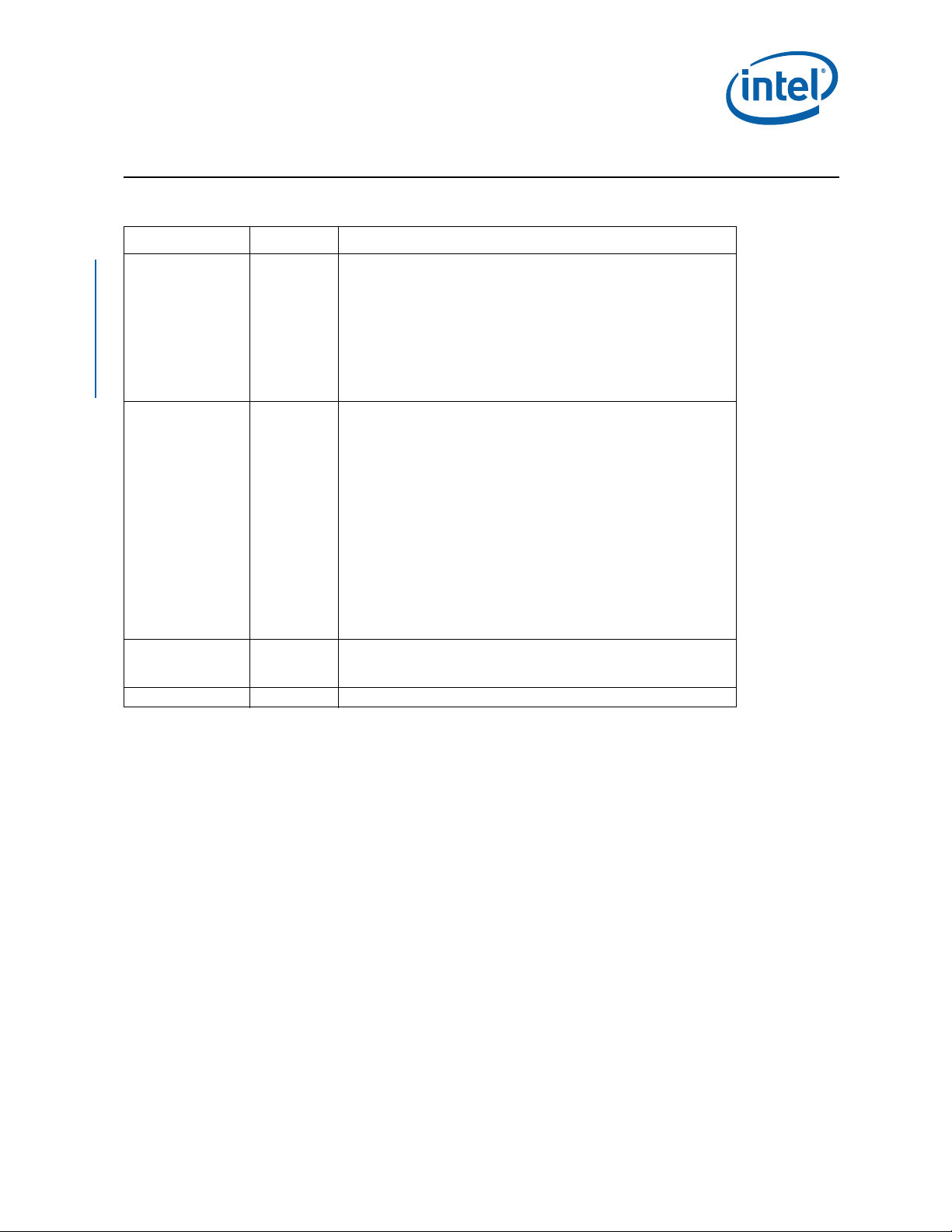
1.1 Content Overview
Chapter Name Description
Chapter 1.0, “Introduction” Conventions used in this manual and related documentation
Chapter 2.0, “System Architecture” System architectural block diagram and system memory map
Chapter 3.0, “General Hardware Design
Considerations”
Chapter 4.0, “General PCB Guide” General PCB design practice and layer stack-up description
Chapter 5.0, “General Layout and Routing
Guide”
Chapter 6.0, “PCI Interface Design
Considerations”
Chapter 7.0, “DDR-SDRAM”
Graphical representation of most common peripheral interfaces.
More specific layout and routing recommendations for board
designers
Board-design recommendations when implementing PCI
interface
Board-design recommendations when implementing
DDRI memory interface
®
IXP45X and
®
IXP465 Network
®
IXP45X and Intel®
December 2006 HDD
Document Number: 305261; Revision: 004 9
Intel® IXP45X and Intel® IXP46X Product Line of Network Processors
Page 10
Intel® IXP45X and Intel® IXP46X Product Line of Network Processors—Introduction
1.2 Related Documentation
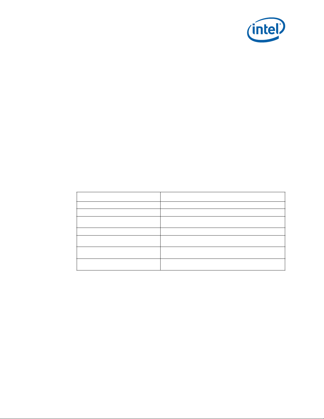
The reader of this design guide should also be familiar with the material and concepts
presented in the following documents:
Title Document #
Hardware-Assisted IEEE 1588* Implementation in the Intel
Product Line White Paper
®
IXP45X and Intel® IXP46X Product Line of Network Processors
Intel
Developer’s Manual
®
Intel
IXP45X and Intel® IXP46X Product Line of Network Processors
Datasheet
®
IXP4XX Product Line of Network Processors Specification
Intel
Update
®
IXP400 Software Programmer’s Guide 252539
Intel
®
Intel
IXP400 Software Specification Update 273795
®
Intel
XScale™ Core Developer’s Manual 273473
®
Intel
IXDP465 Development Platform Documentation Kit N/A
Intel XScale
Intel StrataFlash® Memory (J3) to Intel® Embedded Memory (J3
v.D) Conversion Guide - Application Note 835
Migration Guide for Intel StrataFlash® Synchronous Memory (J3) to
Intel StrataFlash® Embedded Memory (P30 and P33) - Application
Note 812
Migration Guide for Intel StrataFlash® Synchronous Memory (K3/
K18) to Intel StrataFlash® Embedded Memory (P30) - Application
Note 825
Double Data Rate (DDR) SDRAM Specification, 2004; JEDEC Solid
State Technology Association
2
C-Bus Specification from Philips Semiconductors* Available at http://www.nxp.com
I
IEEE 802.3 Specification
IEEE 1149.1 Specification
PCI Local Bus Specification, Rev. 2.2
Universal Serial Bus Specification, Revision 1.1
UTOPIA Level 2 Specification, Revision 1.0
Note: For Intel documentation, see the Intel Technical Documentation Center, available through the
following link:
http://www.intel.com/products/index.htm
®
Microarchitecture Technical Summary —
®
IXP46X
305068
306262
306261
306428
308555
306667
306669
JESD79D
N/A
N/A
N/A
N/A
N/A
®
IXP45X and Intel® IXP46X Product Line of Network Processors
Intel
HDD December 2006
10 Document Number: 305261; Revision: 004
Page 11
®
Introduction—Intel
IXP45X and Intel® IXP46X Product Line of Network Process or s
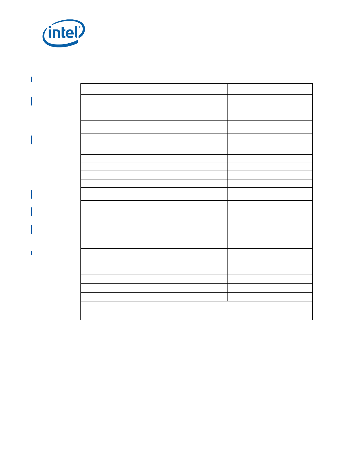
1.3 Acronyms and Abbreviations
Table 1 lists the acronyms and abbreviations used in this guide.
Table 1. List of Acronyms and Abbreviations
Term Explanation
AHB Advanced High-Performance Bus
APB Advanced Peripheral Bus
ATM Asynchronous Transfer Mode
DDR Double Data Rate
EMI Electro-Magnetic Interference
GPIO General Purpose Input/Output
HSS High Speed Serial
I2C Inter-Integrated Circuit
IP Internet Protocol
ISA Instruction Set Architecture
LAN Local Area Network
MII Media-Independent Interface
NPE Network Processor Engine
PCB Printed Circuit Board
PCI Peripheral Component Interface
PHY Physical Layer Interface
PLL Phase-Locked Loop
PMU Performance Monitoring Unit
SDRAM Synchronous Dynamic Random Access Memory
SME Small-to-Medium Enterprise
SMII Serial Media-Independent Interface
SSP Synchronous Serial Protocol
UART Universal Asynchronous Receiver-Transmitter
USB Universal Serial Bus
VTT Termination Voltage Supply
1.4 Overview
The IXP45X/IXP46X network processors are highly integrated devices, capable of
interfacing with most common industry standard peripherals, required for highperformance control applications.
Note: This document discusses all features supported on the Intel
Processor. A subset of these features is supported by certain processors in the IXP45X/
IXP46X product line, such as the Intel
®
IXP460 or Intel® IXP455 network processors.
For details on feature support listed by processor, see the Intel
IXP46X Product Line of Network Processors Datasheet.
Some of the key features of the IXP45X/IXP46X network processors, when used as a
single-chip solution for embedded applications, are as follows:
•Intel XScale
®
Processor (compliant with Intel® StrongARM* architecture) — Up to
667 MHz
December 2006 HDD
Document Number: 305261; Revision: 004 11
Intel® IXP45X and Intel® IXP46X Product Line of Network Processors
®
IXP465 Network
®
IXP45X and Intel®
Page 12

Intel® IXP45X and Intel® IXP46X Product Line of Network Processors—Introduction
• 32-bit PCI interface Master/Target 33/66 MHz
• Device Universal Serial Bus (USB) Controller
• Host Universal Serial Bus (USB) Controller
• DDRI-266 SDRAM (133-MHz Clock, 266-Mbps per data line) — User-enabled ECC,
supports up to 1 Gbyte of external memory
• 32-bit Expansion Bus Interface — Master/Target interface
•Two UART ports
• Up to three Ethernet ports (consult device part number for enabled features) MII/
SMII
• Up to three NPEs
•UTOPIA Level 2 Interface
• Synchronous Serial Port Interface (SSP)
• Two High-Speed Serial Port Interfaces (HSS)
• Inter-Integrated Circuit (IIC or I2C) Interface
• 16 GPIO (General Purpose Input Output)
•Packaging
—544-pin PBGA package
— Commercial temperature (0° to +70° C)
— Extended temperature (-40° to +85° C)
®
For a complete features list and block diagram description, see the Intel
®
Intel
IXP46X Product Line of Network Processors Datasheet.
IXP45X and
Note: Some features require Intel-supplied software. T o determine if a feature is enabled in a
particular software release, refer to the Intel
®
IXP400 Software Specification Update.
A block diagram of all major internal hardware components of the IXP465 network
processor is given in Figure 1. The illustration also shows how the components
interface with each other through the various bus interfaces such as the North AHB,
South AHB, and APB.
®
IXP45X and Intel® IXP46X Product Line of Network Processors
Intel
HDD December 2006
12 Document Number: 305261; Revision: 004
Page 13
Introduction—Intel
®
Figure 1. Intel
UTOPIA 2/MII/SMII
IXP45X and Intel® IXP46X Product Line of Network Process or s
®
IXP465 Component Block Diagram
HSS 0
HSS 1
NPE A
16 GPIO
MII/SMII
MII/SMII
IEEE 1588
I2C
SSP
USB Device
Version 1.1
UART 0
921 KBaud
UART 1
921 KBaud
GPIO
Interrupt
Controller
IBPMU
AES/DES/SHA/
Cryptography
Unit
APB 66.66 MHz x 32 Bits
Hardware RNG
Hashing SHA1
Exponentiation Unit
AHB Slave /
APB
Master
Bridge
USB-Host
Controller V. 2.0
High-Speed is not
Supported
NPE B
NPE C
MD-5
North AHB 133.32 MHz x 32 bits
North AHB
Arbiter
Queue
Manager
AHB/AH B
Bridge
South AHB 133.32 MHz x 32 bits
South AHB
Arbiter
Expansion Bus
Controller
PCI C ont ro ller
DDRI Memory
Controller Unit
MPI
133 MHz x 64
Intel XScale® Processor
32-Kbyte I -Cache
32-Kbyte D-Cache
2-Kbyte Mini D-Cache
32 Bit + ECC
Timers
32 bit at 33/66 MHz8/16/32 bit + Parity
Slave Only
Master on South AHB
Master on North AHB
Bus Arbiters
AHB Slave / APB Master
B3777 -007
Note: Figure 1 shows the Intel® IXP465 Network Processor. For details on feature support
listed by processor, see the Intel
®
IXP45X and Intel® IXP46X Product Line of Network
Processors Datasheet.
December 2006 HDD
Document Number: 305261; Revision: 004 13
Intel® IXP45X and Intel® IXP46X Product Line of Network Processors
Page 14

Intel® IXP45X and Intel® IXP46X Product Line of Network Processors—Introduction
1.5 Typical Applications
• High-performance DSL modem
• High-performance cable modem
•Residential gateway
•SME router
• Integrated access device (IAD)
•Set-top box
• DSLAM
• Access points — 802.11a/b/g
• Industrial controllers
• Network printers
•VoIP Gateways
®
IXP45X and Intel® IXP46X Product Line of Network Processors
Intel
HDD December 2006
14 Document Number: 305261; Revision: 004
Page 15

System Architecture—Intel
®
IXP45X and Intel® IXP46X Product Line of Network Processors
2.0 System Architecture
2.1 System Architecture Description
The Intel® IXP45X and Intel® IXP46X Product Line of Network Processors are multifunction processors that integrate the Intel XScale
compliant) with highly integrated peripheral controllers and intelligent network
processor engines.
The processor is a highly integrated design, manufactured with Intel’s 0.18-micron
production semiconductor process technology. This process technology — along with
numerous, dedicated-function peripheral interfaces and many features with the Intel
XScale processor — addresses the needs of many system applications and helps reduce
system costs. The processors can be configured to meet many system application and
implementation needs.
Figure 2 illustrates one of many applications for which the IXP45X/IXP46X network
processors can be implemented. For detailed functional descriptions, see the Intel
IXP45X and Intel
®
IXP46X Product Line of Network Processors Developer’s Manual.
2.2 System Memory Map
For a complete memory map and register description of each individual module, refer
to the Intel
Developer’s Manual.
®
IXP45X and Intel® IXP46X Product Line of Network Processors
®
Processor (ARM* architecture
®
February 2007 HDD
Document Number: 305261; Revision: 004 15
Intel® IXP45X and Intel® IXP46X Product Line of Network Processors
Page 16
Intel® IXP45X and Intel® IXP46X Product Line of Ne twork Processors—System Architecture
Figure 2. Intel® IXP465 Example System Block Diagram
JTAG
Header
Flash
32 Mbyte
Board
Configuration
Reset Logic
CS_N0
D[31:0]
A[24:0]
Ex pansion Bus
®
Intel
IXP46X Product
SDRAM Memory Bus
RAS, CAS, WE, CS,CLK
Line of Network
LCD/LED
Diagnostics
Display
Buff
Processors
DDR
CB[7:0]
D[31:0]
BA[1:0]
A[13:0]
HSS 1
SSP CODEC or
DDR
DDR
SDRAM
SDRAM
SDRAM
16Mx4x16
DDR
16Mx4x16
16Mx4x16
512 Mbyte
SDRAM
512 Mbyte
512 Mbyte
(Four Chips)
Max 1 Gbyt e
(Four Chips)
(Four Chips)
SLIC/CODEC or
T1/E1/J1 FramerHSS 0
A/D
DB9
DB9
RJ45
Port 0
RJ45
Port 2
RS 232
Serial Port 0
RS 232
Serial Port 1
10/100
PHYs
Up to 3Ports
USB Host
Connector
USB Device
Connector
I2C
UTOPIA Level 2
Clock Buff er
3-MII/
3-SMII/
PCI Bus
USB v2.0 3.3 V
USB v1.1
Transparent PCI Bridge
PCI Slots
Ether net
Clocks
I2C
cPCI Bus
cPCI J2
cPCI J1
2.5 V
1.3 V
xDSL
xDSL
PCI
Clock
Power Supply
xDSL
xDSL
PLL
OSC
B4835 -002
®
IXP45X and Intel® IXP46X Product Line of Network Processors
Intel
HDD February 2007
16 Document Number: 305261; Revision: 004
Page 17
General Hardware Design Considerations—Intel
Network Processors
®
IXP45X and Intel® IXP46X Product Line of
3.0 General Hardware Design Considerations
This chapter contains information for implementing and interfacing to major hardware
blocks of the Intel
®
IXP45X and Intel® IXP46X Product Line of Network Processors.
Such blocks include DDR SDRAM, Flash, SRAM, Ethernet PHYs, UART and most other
peripherals interfaces. Signal definition tables list resistor recommendations for pullups and pull-downs.
Features disabled by a specific part number, do not require pull-ups or pull-downs.
Therefore, all pins can be left unconnected. Features enabled by a specific part number
and required to be Soft Fuse-disabled, only require pull-ups or pull-downs in the clock-
input signals. Other conditions may require pull-up or pull-down resistors for
configuration purposes at power on or reset. Likewise, open-collector outputs must be
pulled-high.
Warning: The IXP45X/IXP46X network processors’ I/O pins are 3.3 V only, except for DDR
SDRAM which is 2.5 V. None of the I/Os are 5-V tolerant.
Table 2 gives the legend for interpreting the Type field used in this chapter’s signal-
definition tables.
Table 2. Signal Type Definition s
Symbol Description
I Input pin only
O Output pin only
I/O Pin can be either an input or output
OD Open-drain pin
TRI Tri-State pin
PWR Power pin
GND Ground pin
3.1 Soft Fusible Features
Soft Fuse Enable/Disable is a method to enable or disable features in hardware,
virtually disconnecting the hardware modules from the processor.
Some of the features offered in the IXP45X/IXP46X product line can be Sof t Fus e
Enabled/Disabled during boot. It is recommended that if a feature is not used in the
design, the feature be Soft disabled. This helps reduce power and maintain the part
running at a cooler temperature. When Soft Fuse Disabled, a pull-up resistor must be
connected to each clock input pins of the disabled feature interface. All other signals
can be left unconnected.
Soft Fuse Enable/Disable can be done by writing to EXP_UNIT_FUSE_RESET register,
for more information refer to the Intel
Network Processors Developer’s Manual and review the register description.
February 2007 HDD
Document Number: 305261; Revision: 004 17
®
IXP45X and Intel® IXP46X Product Line of
Intel® IXP45X and Intel® IXP46X Product Line of Network Processors
Page 18
Intel® IXP45X and Intel® IXP46X Product Line of Network Processors—General Hardware
Table 3. Soft Fusible Features
Name Description
PCI The complete bus must be enabled or disable.
HSS0/1 Can only be disable as a pair.
UTOPIA
ETHERNET
USB Host Each USB can be Enable separately.
USB Device Each USB can be Enable separately.
DDR ECC DDR can be disabled separately form the rest of the DDR interface.
If enabling UTOPIA, MACs on NPE A are disabled.
If enabling MACs on NPE A, UTOPIA are disabled.
Can Enable either MII MACs or SMII MACs, but not both at the same time. Enable of MACs
can be separately done per each NPE.
3.2 DDR-266 SDRAM Interface
The IXP45X/IXP46X network processors support unbuffered, DDR-266 SDRAM
technology, capable of addressing two memory banks (one bank per CS). Each bank
can be configured to support 32/64/128/256/512-Mbyte for a total combined memory
support of 1 Gbyte.
Design Considerations
The device supports non-ECC and ECC for error correction, which can be enable or
disable by software as required. Banks have a bus width of 32 bits for non ECC or
40 bits for ECC enable (32-bit data + 8-bit ECC).
For a complete feature list, see the Intel
®
IXP45X and Intel® IXP46X Product Line of
Network Processors Datasheet.
General DDR SDRAM routing guidelines can be found in Section 7.1.7, “Routing
Guidelines” on page 88. For more detailed information, see the PC266 DDR SDRAM
specification.
3.2.1 Signal Interface
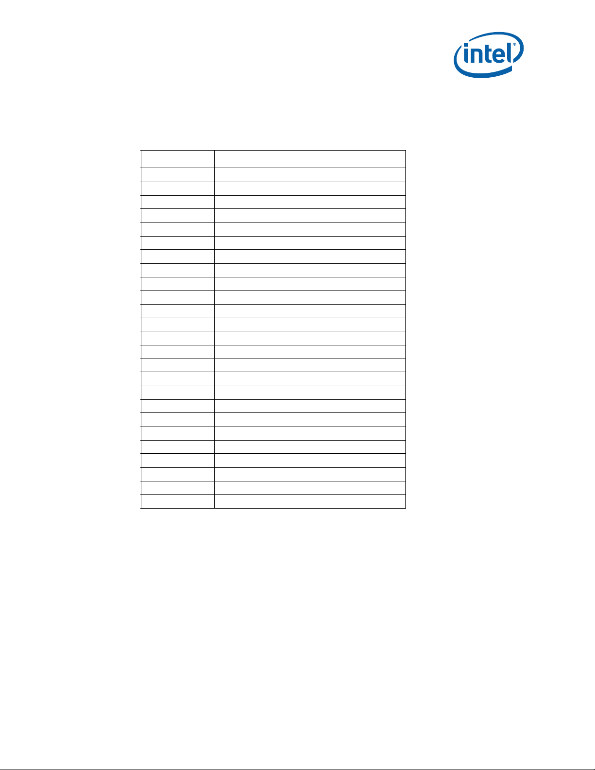
Table 4. DDR SDRAM Interface Pin Description (Sheet 1 of 2)
Name
DDRI_CK[2:0] O
DDRI_CK_N[2:0] O Same as above No
DDRI_CS_N[1:0] O
DDRI_RAS_N O
DDRI_CAS_N O
Input
Outpu
t
Device-Pin Connection
Connect a pair of differential clock
signals to every device; When
using both banks, daisy chain
devices with same data bit
sequence.
Use the same CS to control 32-bi t
data + 8-bit ECC, per bank
The RAS signal must be connected
to each device in a daisy chain
manner
The CAS signal must be connected
to each device in a daisy chain
manner
VTT
Terminatio
n
No
Yes
Yes
Yes
DDR SDRAM Clock Out — Provides the positive
differential clocks to the external SDRAM
memory subsystem.
DDR SDRAM Clock Out — Provides the
negative differential clocks to the external
SDRAM memory subsystem.
Chip Select — Must be asserted for all
transactions to the DDR SDRAM device. One
per bank.
Row Address Strobe — Indicates that the
current address on DDRI_MA[13:0] is the row.
Column Address Strobe — Indicates that the
current address on DDRI_MA[13:0] is the
column.
Description
®
IXP45X and Intel® IXP46X Product Line of Network Processors
Intel
HDD February 2007
18 Document Number: 305261; Revision: 004
Page 19
General Hardware Design Considerations—Intel
Network Processors
®
IXP45X and Intel® IXP46X Product Line of
Table 4. DDR SDRAM Interface Pin Description (Sheet 2 of 2)
Name
DDRI_WE_N O
DDRI_DM[4:0] O
DDRI_BA[1:0] O
DDRI_MA[13:0] O
DDRI_DQ[31:0] I/O
DDRI_CB[7:0] I/O Connect to ECC memory devices. Yes
DDRI_DQS[4:0] I/O
DDRI_CKE[1:0] O
DDRI_RCVENOUT_N O
DDRI_RCVENIN_N I Same as above No
DDRI_RCOMP O Tied off to a resistor
DDRI_VREF I VCCM/2 VCCM/2
Input
Outpu
t
Device-Pin Connection
The WE signal must be connected
to each device in a daisy chain
manner
Connect to each DM device pin.
For the 8-bit devices connect one
DM signal per device.
For the 16-bit devices connect two
DM signal per device (depending
on how many data bits are being
used).
The BA signals must be connected
to each device in a daisy chain
manner.
All address signals need to be
connected to each device in a
daisy chain manner.
Need to be connected in parallel
to achieve a 32-bit bus width.
Connect DQS[3:0] to devices wi th
data signals and DQS[4] to
devices with ECC signals.
Use one CKE per bank, never mix
the CKE on the same bank. Use
CKE[0] for bank0 and CKE[1] for
bank1
Connect RCVEOUT to RCVENIN
and follow note on pin description
in this table.
VTT
Terminatio
n
Yes
Yes
Yes
Yes
Yes Data Bus — 32-bit wide data bus.
Yes
Yes
No
Tied off to a
resistor
Description
Write Strobe — Defines whether or not the
current operation by the DDR SDRAM is to be
a read or a write.
Data Bus Mask — Controls the DDR SDRAM
data input buffers. Asserting DDRI_WE_N
causes the data on DDRI_DQ[31:0] and
DDRI_CB[7:0] to be written into the DDR
SDRAM devices.
DDRI_DM[4:0] controls this operation on a
per-byte basis. DDRI_DM[3:0] are intended to
correspond to each byte of a word of data.
DDRI_DM[4] is intended to be utilized for the
ECC byte of data.
DDR SDRAM Bank Selects — Controls which of
the internal DDR SDRAM banks to read or
write. DDRI_BA[1:0] are used for all
technology types supported.
Address bits 13 through 0 — Indicates the row
or column to access depending on the state of
DDRI_RAS_N and DDRI_CAS_N.
ECC Bus — Eight-bit error correction code
which accompanies the data on
DDRI_DQ[31:0].
When ECC is disabled and not being used in a
system design, these signals can be left unconnected.
Data Strobes Differential — Strobes that
accompany the data to be read or written from
the DDR SDRAM devices. Data is sampled on
the negative and positive edges of these
strobes. DDRI_DQS[3:0] are intended to
correspond to each byte of a word of data.
DDRI_DQS4] is intended to be utilized for the
ECC byte of data.
Clock enables — One clock after
DDRI_CKE[1:0] is de-asserted, data is latched
on DQ[31:0] and DDRI_CB[7:0]. Burst
counters within DDR SDRAM device are not
incremented. De-asserting this signal places
the DDR SDRAM in self-refresh mode. For
normal operation, DDRI_CKE[1:0] must be
asserted.
RECEIVE ENABLE OUT must be connected to
DDRI_RCVENIN_N signal of the IXP45X/
IXP46X product line and the propagation delay
of the trace length must be matched to the
clock trace plus the average DQ Traces.
RECEIVE ENABLE IN provides delay
information for enabling the input receivers
and must be connected to the
DDRI_RCVENOUT_N signal
IXP46X network processors.
20 Ohm Resistor connected to ground used for
process/temperature adjustments.
DDR SDRAM Voltage Reference — is used to
supply the reference voltage to the di fferential
inputs of the memory controller pins.
of the IXP45X/
February 2007 HDD
Document Number: 305261; Revision: 004 19
Intel® IXP45X and Intel® IXP46X Product Line of Network Processors
Page 20

Intel® IXP45X and Intel® IXP46X Product Line of Network Processors—General Hardware
3.2.2 DDR SDRAM Memory Interface
The IXP45X/IXP46X network processors support compatible DDR-266 SDRAM, 8- and
16-bit wide devices, with a total bus width of 32 bits. Only 32-bit-wide accesses are
supported.
The maximum supported memory is 1 Gbyte, configured by enabling both physical
banks of DDR-266 SDRAM devices. Each bank can be composed of four 1-Gbit (32 Mbit
X 8 X 4) devices and use one chip-selects per bank. The minimum supported memory
is 32 Mbyte, configured by enabling a single physical bank of DDR-266 SDRAM devices.
The bank would consist of two 128-Mbit (2 Mbit X 16 X 4) devices and using a single
chip-select.
All supported memory configurations are listed in T able 28 on page 78. Remember that
these are all non-buffer devices, as the IXP45X/IXP46X network processors only
support non-buffer memory devices.
For a complete description on how the IXP45X/IXP46X network processors interface to
DDR SDRAM, see Chapter 7.0, “DDR-SDRAM”.
3.2.3 DDR SDRAM Initialization
For instructions on DDR SDRAM initialization, refer to the Intel® IXP45X and Intel®
IXP46X Product Line of Network Processors Developer’s Manual and its section titled
“DDR SDRAM Initialization.”
Design Considerations
3.3 Expansion Bus
The Expansion Bus of the IXP45X/IXP46X network processors is specifically designed
for compatibility with Intel- and Motorola*-style microprocessor interfaces and Texas
Instruments* DSP standard Host-Port Interfaces* (HPI).
The expansion bus controller includes a 25-bit address bus and a 32-bit wide data path,
running at a maximum speed of 80 MHz from an external clock oscillator. The bus can
be configure to support the following target devices:
• Intel multiplexed • Intel non-multiplexed
•Intel StrataFlash
• Micron* Flow-Through ZBT • Motorola multiplexed
• Motorola non multiplexed • Texas Instruments* Host Port Interface
The expansion bus controller also has an arbiter that supports up to four external
devices that can master the expansion bus. External masters can be used to access
external slave devices that reside on the expansion bus, including access to internal
memory mapped regions within the IXP45X/IXP46X network processors.
All supported modes are seamless and no additional glue logic is required. Other cycle
types may be supported by configuring the Timing and Control Register for Chip Select.
Applications having less than 32 data bits may connect to less than the full 32 bits.
Devices with wider than 32-bit data bus are not supported. A total of eight chip selects
are supported with an address space of up to 32 Mbytes per chip select.
®
• Synchronous Intel StrataFlash
®
Memory
(HPI)
®
IXP45X and Intel® IXP46X Product Line of Network Processors
Intel
HDD February 2007
20 Document Number: 305261; Revision: 004
Page 21
General Hardware Design Considerations—Intel
Network Processors
®
IXP45X and Intel® IXP46X Product Line of
3.3.1 Signal Interface
Table 5. Expansion Bus Signal Recommendations
Name
EX_CLK I No Use series termination resistor, 10Ω to 33Ω at the source.
EX_ALE TRI O No Use series termination resistor, 10Ω to 33Ω at the source.
EX_ADDR[24:0] I/O Yes
EX_WR_N I/O No Use series termination resistor, 10Ω to 33Ω at the source.
EX_RD_N I/O No Use series termination resistor, 10Ω to 33Ω at the source.
EX_CS_N[7:0] I/O Yes
EX_DATA[31:0] I/O No
EX_BE_N[3:0] I/O No
EX_IOWAIT_N I Yes Should be pulled high through a 10-KΩ resistor when not being utilized in the system.
EX_RDY_N[3:0] I Yes Should be pulled high through a 10-KΩ resistor when not being utilized in the system.
EX_PARITY[3:0] I/O No
EX_REQ_N[3:1] I Yes Should be pulled high through a 10-KΩ resistor when not being utilized in the system.
EX_REQ_GNT_N I Yes Should be pulled high through a 10-KΩ resistor when not being utilized in the system.
EX_GNT_N[3:1] O No
EX_GNT_REQ_N O No
EX_SLAVE_CS_N I Yes Should be pulled high through a 10-KΩ resistor when not being utilized in the system.
EX_BURST I Yes Should be pulled high through a 10-KΩ resistor when not being utilized in the system.
EX_WAIT_N TRI O No
Input
Output
Pull
Up
Down
Use 4.7-KΩ resistors for pull-downs; required for boot strapping for initial configuration of
Configuration Register 0. Pull-ups are not required as for when the system comes out of
reset, all bits are initially set HIGH. For more details, see Table 6.
For additional details on address strapping, see the Intel
Product Line of Network Processors Developer’s Manual.
Use series termination resistor, 10Ω to 33Ω at the source.
Use 10KΩ resistors pull-ups to ensure that the signal remains de-asserted.
Recommendations
®
IXP45X and Intel® IXP46X
3.3.2 Reset Configuration Straps
At power up or whenever RESET_IN_N is asserted, the Expansion-bus address outputs
are switched to inputs and the state of the inputs are captured and stored in
Configuration Register 0, bits 24 through 0. This occurs when PLL_LOCKED is deasserted.
The strapping of Expansion-bus address pins can be done by placing external pull-down
resistors at the required address pin. It is not required to use external pull-up resistors,
by default upon reset all bits on Configuration Register 0 are set High, unless an
external pull down is used to set them Low. For example to register a bit low or high in
the Configuration Register 0, do the following:
Place an external 4.7-KΩ pull-down resistor to set a bit LOW.
No external pull-up is required, by default upon reset, bits are set HIGH.
The state of the boot-strapping resistor is register on the first cycle after the
synchronous de-assertion of the reset signal. These bits can be read or written as
needed for desired configurations. It is recommended that only Bit 31, Memory Map, be
changed from 1 to 0 after execution of boot code from external flash.
February 2007 HDD
Document Number: 305261; Revision: 004 21
Intel® IXP45X and Intel® IXP46X Product Line of Network Processors
Page 22
Intel® IXP45X and Intel® IXP46X Product Line of Network Processors—General Hardware
For a complete bit description of Configuration Register 0, see the Intel® IXP45X and
®
Intel
IXP46X Product Line of Network Processors Developer’s Manual.
Design Considerations
Table 6. Boot/Reset Strapping Configuration (Sheet 1 of 2)
Name Function Description
EX_ADDR[24] (Reserved) (Reserved)
Intel XScale
EX_ADDR[23:21]
EX_ADDR[20:17] Customer Customer-defined bits. (Might be used for board revision.)
EX_ADDR[16:11] (Reserved) (Reserved)
EX_ADDR[10] IOWAIT_CS0
EX_ADDR[9] EXP_MEM_DRIVE Refer to table found in EX_ADDR[5].
EX_ADDR[8] USB Clock
EX_ADDR[7] 32_FLASH Refer to table found in EX_ADDR[0]
EX_ADDR[6] EXP_ARB
EX_ADDR[5] EXP_DRIVE
EX_ADDR[4] PCI_CLK
EX_ADDR[3] (Reserved) (Reserved). EX_ADDR[3] must not be pulled down during address strapping.
Processor
Clock Set[2:0]
®
Allows changing Intel XScale
settings. However cannot be used to over-clock core speed.
1 = EX_IOWAIT_N is sampled during the read/write expansion bus cycles for Chip
Select 0.
0 = EX_IOWAIT_N is ignored for read and write cycles to Chip select 0 if
EXP_TIMING_CS0 is configured to Intel mode.
Typically, IOWAIT_CS0 must be pulled down to Vss when attaching a Synchronous
Intel StrataFlash
Intel mode and EX_IOWAIT_N is an unknown value for Synchronous Intel
StrataFlash.
If the board does not connect the Synchronous Intel StrataFlash WAIT pin to
EX_WAIT_N (and the board guarantees EX_IOWAIT_N is pulled up), the value of
IOWAIT_CS0 is a don’t-care, since EX_IOWAIT_N will not be asserted.
When EXP_TIMING_CS0 is reconfigure to Intel Synchronous mode during boot-up
(for synchronous Intel chips), the expansion bus controller ignores EX_IOWAIT_N
during read and write cycles since the WAIT functionality is determined from the
EXP_SYNCINTEL_COUNT and EXP_TIMING_CS registers.
Controls the USB clock select.
1 = USB Host/Device clock is generated internally
0 = USB Device clock is generated from GPIO[0].
USB Host clock is generated from GPIO[1]. When generating a spread spectrum
clock on OSC_IN, GPIO[0] can be driven from the system board to generate a
48-MHz clock for the USB Device and GPIO[1] can be driven from the system board
to generate a 60-MHz clock for the USB Host.
Configures the Expansion bus arbiter.
0 = External arbiter for Expansion bus.
1 = Expansion bus controller arbiter enabled
Expansion bus low/medium/high drive strength. The drive strength depends on
EXP_DRIVE and EXP_MEM_DRIVE configuration bits.
B9. B5
--------------------------------------------------------------------------------------0 . . 0 Reserved
0 . . 1 Medium Drive
1 . . 0 Low Drive
1 . . 1 High Drive
Sets the clock speed of the PCI Interface
0 = 33 MHz
1 = 66 MHz
®
on Chip Select 0 since the default mode for EXP_TIMING_CS0 is
®
Processor clock speed. This overrides device fuse
®
IXP45X and Intel® IXP46X Product Line of Network Processors
Intel
HDD February 2007
22 Document Number: 305261; Revision: 004
Page 23

General Hardware Design Considerations—Intel
Network Processors
®
IXP45X and Intel® IXP46X Product Line of
Table 6. Boot/Reset Strapping Configuration (Sheet 2 of 2)
Name Function Description
Enables the PCI Controller Arbiter
EX_ADDR[2] PCI_ARB
EX_ADDR[1] PCI_HOST
EX_ADDR[0] 8/16_FLASH
0 = PCI arbiter disabled
1 = PCI arbiter enabled
Configures the PCI Controller as PCI Bus Host
0 = PCI as non-host
1 = PCI as host
Specifies the data bus width of the FLASH memory device found on Chip Select 0.
The data bus is based upon bits 0 and 7 of Configuration Register 0.
32_FLASH 8/16_FLASH Data bus size
B7 . B0
------------------------------------------------------------------------------------0 . . 0 16-bit
0 . . 1 8-bit
1 . . 0 (Reserved)
1 . . 1 32-bit
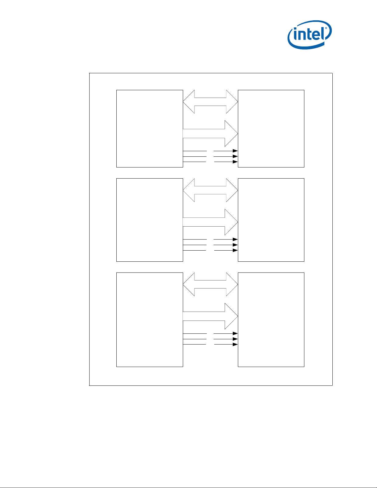
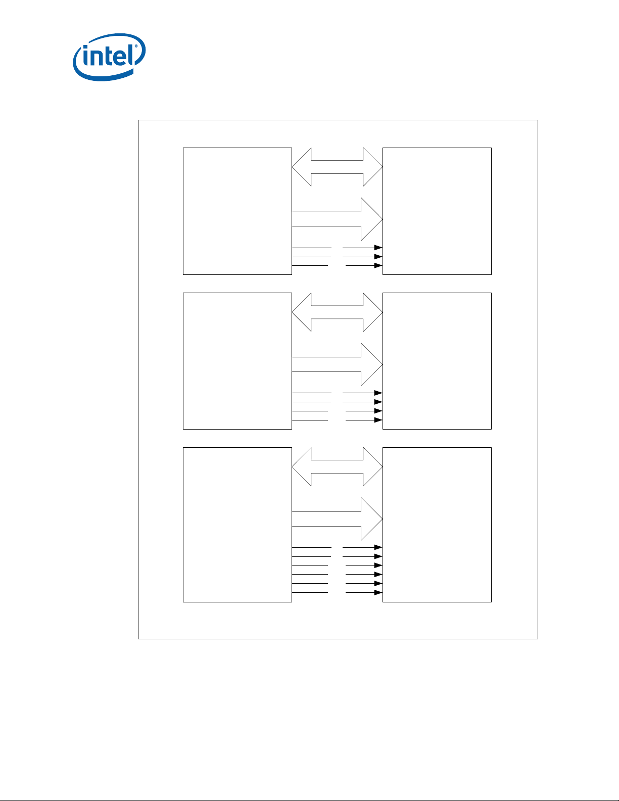
3.3.3 8-Bit Device Interface
The IXP45X/IXP46X network processors support 8-bit-wide data bus devices (byte
mode). For Intel interface cycles, the data lines and control signals can be connected as
shown in Figure 3 on page 25 and Figure 4 on page 26. During byte mode accesses,
the remaining data signals not being used EX_DAT A[31:8], are driven by the processor
to an unpredictable state on WRITE cycles and tri-stated during READ cycles.
When booting an 8-bit flash device, the expansion bus must be configured during reset
to the 8-bit mode (see Configuration Register 0). To accomplish this, boot-strapping is
required in certain address pins of the Expansion bus. For example, as in this case
when booting of an 8-bit flash device, bit 0 and 7 of Configuration Register 0 must be
set as follows:
Bit 0 = 1. By default this bit is set high when coming off reset or any time reset is
asserted.
Bit 7 = 0. This can be done by placing an external 4.7-KΩ pull-down resistor to pin
EX_ADDR[7].
If it is required to change access mode, after the system has booted, and during
normal operation; the Timing and Control Register for Chip Select must be configured
to perform the desired mode access. For a complete description on accomplishing this
refer to the “Expansion Bus” chapter in the Intel
Line of Network Processors Developer’s Manual.
3.3.4 16-Bit Device Interface
The IXP45X/IXP46X network processors support 16-bit wide data bus devices (16-bit
word mode). For Intel interface cycles, the data lines and control signals can be
connected as shown in Figure 3 on page 25 and Figure 4 on page 26. During word
mode accesses, the remaining data signals not being used EX_DAT A[31:16], are driven
by the processor to an unpredictable state on WRITE cycles and tri-stated during READ
cycles.
When booting a 16-bit flash device, the expansion bus must be configured during reset
to the 16-bit mode (see Configuration Register 0). To accomplish this, boot-strapping is
required in certain address pins of the Expansion bus.
®
IXP45X and Intel® IXP46X Product
February 2007 HDD
Document Number: 305261; Revision: 004 23
Intel® IXP45X and Intel® IXP46X Product Line of Network Processors
Page 24

Intel® IXP45X and Intel® IXP46X Product Line of Network Processors—General Hardware
For example, as in this case when booting of a 16-bit flash device, bit 0 and 7 of
Configuration Register 0 must be set as follows:
• Bit 0 = 0.
This can be done by placing an external 4.7-KΩ pull-down resistor to pin
EX_ADDR[0].
• Bit 7 = 0.
This can be done by placing an external 4.7-KΩ pull-down resistor to pin
EX_ADDR[7].
If it is required to change access mode, after the system has booted, and during
normal operation; the Timing and Control Register for Chip Select must be configured
to perform the desired mode access. For a complete description on accomplishing this
refer to the “Expansion Bus” chapter in the Intel
Line of Network Processors Developer’s Manual.
3.3.5 32-Bit Device Interface
The IXP45X/IXP46X network processors support 32-bit wide data bus devices (32-bit
word mode). For Intel interface cycles, the data lines and control signals can be
connected as shown in Figure 3 on page 25 and Figure 4 on page 26.
When booting a 32-bit flash device, the expansion bus must be configured during reset
to the 32-bit mode (see Configuration Register 0). To accomplish this, boot-strapping is
required in certain address pins of the Expansion bus. For example, as in this case
when booting of a 32-bit flash device, bit 0 and 7 of Configuration Register 0 must be
set as follows:
• Bit 0 = 1.
By default this bit is set high when coming off reset or any time reset is asserted.
• Bit 7 = 1.
By default this bit is set high when coming off reset or any time reset is asserted.
Design Considerations
®
IXP45X and Intel® IXP46X Product
If it is required to change access mode, after the system has booted, and during
normal operation; the Timing and Control Register for Chip Select must be configured
to perform the desired mode access. For a complete description on accomplishing this
refer to the “Expansion Bus” chapter in the Intel
®
IXP45X and Intel® IXP46X Product
Line of Network Processors Developer’s Manual.
®
IXP45X and Intel® IXP46X Product Line of Network Processors
Intel
HDD February 2007
24 Document Number: 305261; Revision: 004
Page 25
General Hardware Design Considerations—Intel
Network Processors
®
IXP45X and Intel® IXP46X Product Line of
Figure 3. 8/16/32-Bit Device Interface: No Byte-Enable
EX_DAT A[31:0]
Intel® IXP46X
Product Line of
N etwo rk Pro cessor s
EX_ADDR[24:0]
EX_CS_N
EX_RD_N
EX_WR_N
EX_DAT A[31:0]
®
Intel
IXP46X
Product Line of
Netw or k P r ocesso r s
EX_ADDR[24:0]
EX_CS_N
EX_RD_N
EX_WR_N
EX_DATA[7:0]
EX_ADDR[24:0]
CS
OE
WR
EX_DAT A[15:0]
EX_ADDR[24:0]
CS
OE
WR
DATA[7:0]
8-Bit Device
B yte Access
ADDR[24:0]
CS_N
OE_N
WR_N
DATA[15:0]
16-Bit Device
16 -Bit-Word Access
ADDR[24:0]
CS_N
OE_N
WR_N
EX_DAT A[31:0]
®
Intel
IXP46X
Product Line of
Netw or k P r ocesso r s
EX_ADDR[24:0]
EX_CS_N
EX_RD_N
EX_WR_N
February 2007 HDD
Document Number: 305261; Revision: 004 25
EX_DAT A[31:0]
DATA[31:0]
32-Bit Device
32 -Bit-Word Access
EX_ADDR[24:0]
CS
OE
WR
Intel® IXP45X and Intel® IXP46X Product Line of Network Processors
ADDR[24:0]
CS_N
OE_N
WR_N
B4095-002
Page 26
Intel® IXP45X and Intel® IXP46X Product Line of Network Processors—General Hardware
Figure 4. 8/16/32-Bit Device Interface: Byte Enable
Design Considerations
EX_DAT A[31:0]
Intel® IXP46X
Product Line of
N etwo rk Pro cessor s
EX_ADDR[24:0]
EX_CS_N
EX_RD_N
EX_BE_N0
EX_DAT A[31:0]
®
Intel
IXP46X
Product Line of
N etwo rk Pro cessor s
EX_ADDR[24:0]
EX_CS_N
EX_RD_N
EX_BE_N0
EX_BE_N1 WR_N1
EX_DAT A[7:0]
EX_ADDR[24:0]
CS
OE
WR0
EX_DAT A[15:0]
EX_ADDR[24:0]
CS
OE
WR0
WR1
DATA[7:0]
8-Bit Device
Byte Access
ADDR[24:0]
CS_N
OE_N
WR_N
DATA[15:0]
16-Bit Device
16 -Bi t-Word Access
ADDR[24:0]
CS_N
OE_N
WR_N0
EX_DAT A[31:0]
®
Intel
IXP46X
Product Line of
N etwo rk Pro cessor s
EX_ADDR[24:0]
EX_CS_N
EX_RD_N
EX_BE_N0
EX_BE_N1 WR_N1
EX_BE_N2 WR_N2
EX_BE_N3 WR_N3
®
IXP45X and Intel® IXP46X Product Line of Network Processors
Intel
HDD February 2007
26 Document Number: 305261; Revision: 004
EX_DAT A[31:0]
EX_ADDR[24:0]
CS
OE
WR0
WR1
WR2
WR3
DATA[31:0]
32-Bit Device
32 -Bi t-Word Access
ADDR[24:0]
CS_N
OE_N
WR_N0
B4096-003
Page 27
General Hardware Design Considerations—Intel
Network Processors
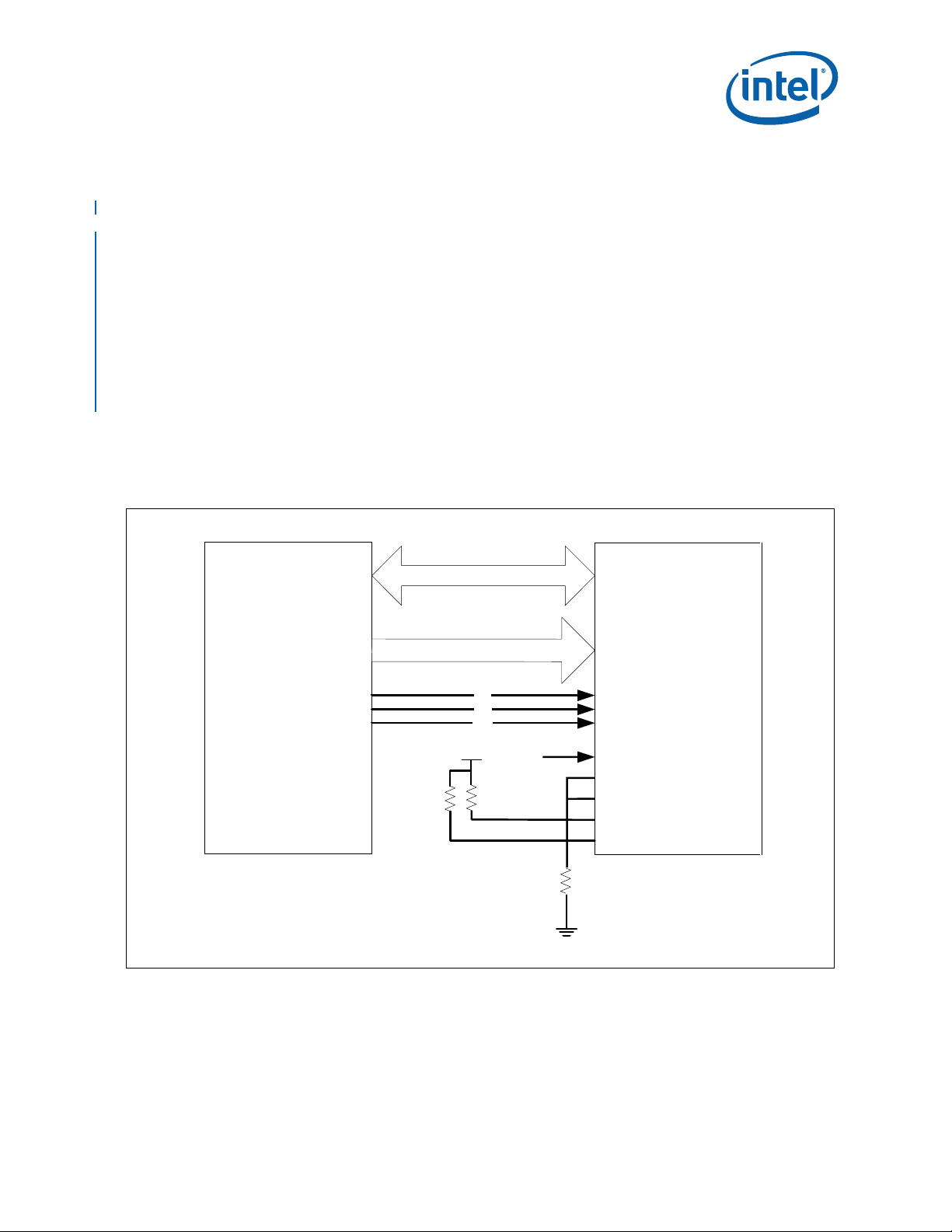
3.3.6 Flash Interface
®
IXP45X and Intel® IXP46X Product Line of
Figure 5 illustrates how a boot ROM is connected to the expansion bus. The flash (ROM)
used in the block diagram is the Intel StrataFlash
32-Mbyte, 16-bit, flash in the 56-TSOP package. The Intel StrataFlash memory
TE28F256J3D is part of the 0.13-micron, 3.3-V Intel StrataFlash memory.
The E28F256J3D supports common flash interface (CFI). For information on migrating
from J3 to J3D Intel StrataFlash memory, see the Intel StrataFlash
®
Embedded Flash Memory (J3 v.D) Conversion Guide - Application Note 835
Intel
(document 308555).
For information on migrating from J3 to P30 Intel StrataFlash memory, see the
Migration Guide for Intel StrataFlash
Memory (P30 and P33) - Application Note 835 (document 308555).
The example in Figure 5 shows a 16-bit flash memory device connected to the IXP45X/
IXP46X network processors. Boot-strapping is required in the address bus, both
EX_ADDR[0] and EX_ADDR[7] need external, 4.7-KΩ pull-down resistors (not shown
on diagram). The pull-down resistors sets Bits 0 and 7 low in the Configuration Register
0. This in turn sets the processor into a 16-bit-mode access.
Figure 5. Flash Interface Example
EX_DAT A[31:0]
Intel® IXP46X
Product Line of
Netw or k Pro cessor s
EX_ADDR[24:0]
®
Memory (J3) to Intel StrataFlash® Embedded
EX_DAT A[15:0]
2
[
X
E
_
4
R
D
:
D
A
®
memory device TE28F256J3D —
®
Memory J3 to
DATA[15:0]
16-Bit Device
16 -Bi t-Wo rd Access
0
]
ADDR[24:0]
EX_CS_N
EX_RD_N
EX_WR_N
4.7 KΩ 4.7 KΩ
CS
OE
WR
3.3 V
RST#
CE0
OE_N
WR_N
Intel® Flash
RP_N
CE1
CE2
BYTE_N
VPEN_N
4. 7 KΩ
B4097- 003
February 2007 HDD
Document Number: 305261; Revision: 004 27
Intel® IXP45X and Intel® IXP46X Product Line of Network Processors
Page 28
Intel® IXP45X and Intel® IXP46X Product Line of Network Processors—General Hardware
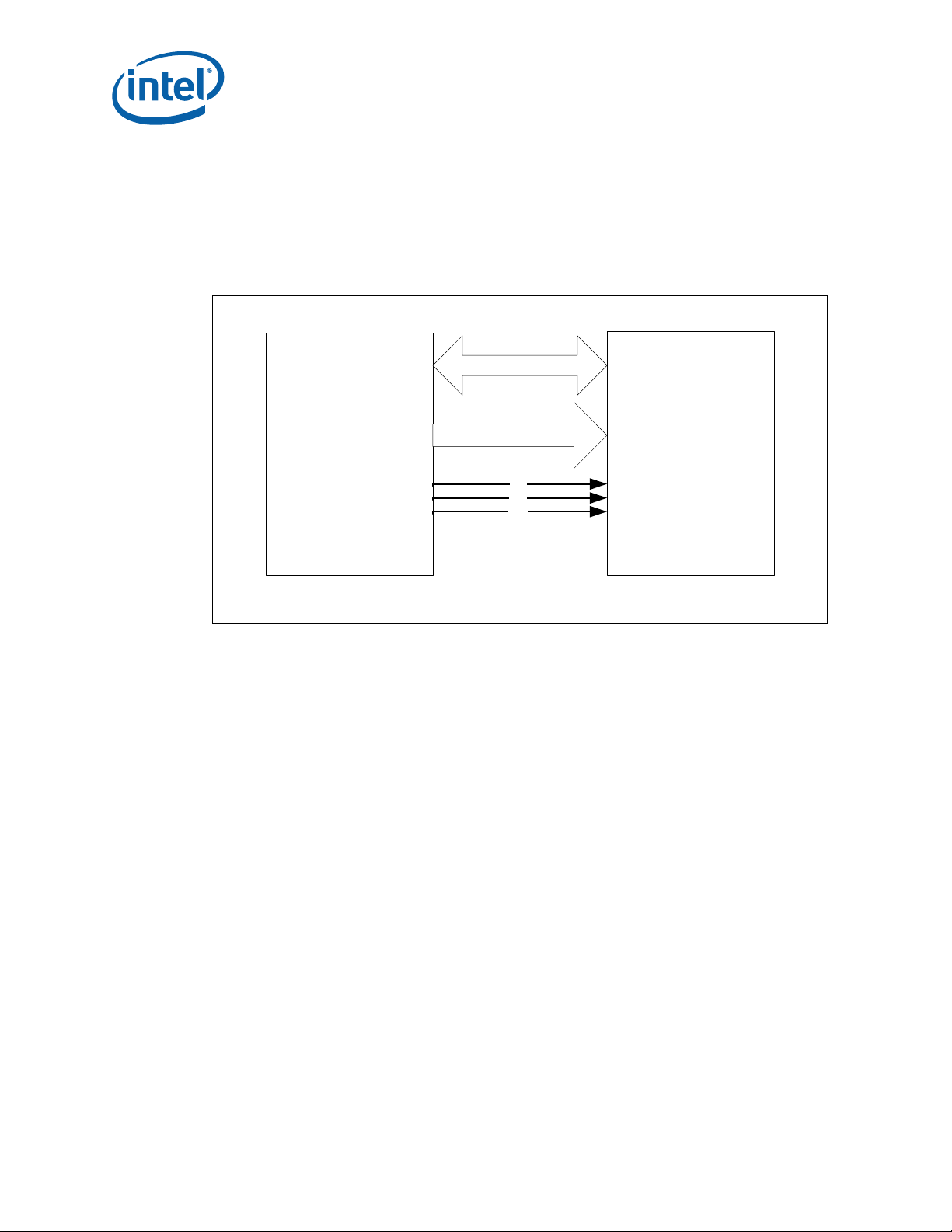
3.3.7 SRAM Interface
A typical connection between an 8-bit SRAM memory device and the IXP45X/IXP46X
network processors expansion bus is shown in Figure 6 on page 28. When attempting
to communicate to this device, the Timing and Control Register for Chip Select must be
configured for proper access. For more information, see the Intel
.
Figure 6. Expansion Bus SRAM Interface
IXP46X Product Line of Network Processors Developer’s Manual.
Design Considerations
®
IXP45X and Intel®
Intel® IXP46X
Product Line of
N etwo rk Pro cesso rs
3.3.8 Design Notes
Care must be taken when loading the bus with too many devices. As more devices are
added, the loading capacity adds up — to the point where timing can become critical.
To account for this, timing on the expansion bus may be adjusted in the Timing and
Control Register for Chip Select. If an edge rises slowly due to low drive strength, the
processors should wait an extra cycle before the value is read. For more information,
see the documentation on Timing and Control Register for Chip Select bits [29:16] in
the Intel
Manual.
®
IXP45X and Intel® IXP46X Product Line of Network Processors Developer’s
EX_DATA[31:0]
EX_ADDR[24:0]
EX_CS_N
EX_RD_N
EX_WR_N
EX_DATA[7:0]
EX_ADDR[18:0]
CS
OE
WR
DATA[7:0]
8-Bit Device
Byte Access
ADDR[18:0]
E#
G#
W#
512 Kbyte-x-8
SRAM
Inte rfa ce
B 4098-003
3.4 UART Interface
The IXP45X/IXP46X network processors provide two dedicated, Universal
Asynchronous Receiver/Transmitter Serial Ports (UARTs). These are high-speed UART s,
capable of supporting baud rates from 1,200 Baud to 921.6 KBaud.
The hardware supports a four-wire interface:
• Transmit Data
• Receive Data
•Request to Send
•Clear to Send
®
IXP45X and Intel® IXP46X Product Line of Network Processors
Intel
HDD February 2007
28 Document Number: 305261; Revision: 004
Page 29
General Hardware Design Considerations—Intel
Network Processors
®
IXP45X and Intel® IXP46X Product Line of
Note: The UART module does not support full modem functionality. However, this can be
implemented, by using GPIO ports to generate DTR, DSR, RI, and DCD and making
some changes to the driver.
3.4.1 Signal Interface
Table 7. UART Signal Recommendations
Name
RXDATA0 I Yes
TXDATA0 O No Serial data output Port 0.
CTS0_N I Yes
RTS0_N O No Request-To-Send Port 0.
RXDATA1 I Yes
TXDATA1 O No Serial data output Port 1.
CTS1_N I Yes
RTS1_N O No Request-To-Send Port 1.
Input
Output
Pull
Up
Down
Serial data input Port 0.
When signal is not being used in the system, this pin should be pulled high with a 10-KΩ
resistor.
Clear-To-Send Port 0.
\When signal is not being used in the system, this pin should be pulled high with a 10-KΩ
resistor.
Serial data input Port 1.
When signal is not being used in the system, this pin should be pulled high with a 10-KΩ
resistor.
Clear-To-Send Port 1.
When signal is not being used in the system, this pin should be pulled high with a 10-KΩ
resistor.
The following figure contain a typical four signal interface between the UART and an
RS-232 transceiver driver, required to interface with external devices. Unused inputs to
the RS-232 driver can be connected to ground. This avoids signals floating to
undetermined states which can cause over heating of the driver leading to permanent
damage.
Recommendations
February 2007 HDD
Document Number: 305261; Revision: 004 29
Intel® IXP45X and Intel® IXP46X Product Line of Network Processors
Page 30
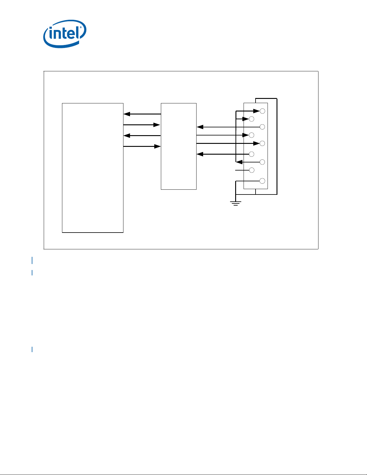
Intel® IXP45X and Intel® IXP46X Product Line of Network Processors—General Hardware
Figure 7. UART Interface Example
CTS1_N
RTS1_N
UART
Interface
RXDATA1
TXDATA1
Intel® IXP46X
Intel® IXP46X
Product Line of
Product Line of
Netw or k P r ocesso r s
N etwo rk Pro cesso rs
OUT4
IN3
OUT3
OUT1
OUT2
IN2
RS-232
Transceiver
IN1
IN4
NC
DB9
Con nector
6
7
8
9
Design Considerations
1 DC D
1
2 RX
3 TX
2
4 DTR
3
5 GND
6 DSR
4
7 RTS
8 CTS
5
9 RI
3.5 MII/SMII Interface
The IXP45X/IXP46X network processors support a maximum of three Ethernet MACs.
Depending on the IXP45X/IXP46X network processors part number used, various
combinations can be used. For the various features that can be enable a variety of
needs, see the Intel
Datasheet.
All MACs contained in the NPEs are compliant to the IEEE 802.3 specification and
handle flow control for the IEEE 802.3Q VLAN specification.
The Management Data Interface (MDI) supports a maximum of 32 PHY addresses. MDI
signals are required to be connected to every PHY chip. Each PHY port is assign a
unique address in the external PHY chip from 0 to 31, totaling a maximum of 32 PHY
addresses. The maximum number of MACs supported by the IXP45X/IXP46X network
processors is three.
The MII interface supports clock rates of 25 MHz for 100-Mbps operation or 2.5 MHz for
10-Mbps operation.
SMII interface supports clock rate of 125 MHz for 10/100-Mbps operation.
General PHY Ethernet devices routing guidelines can be found in Section 5.2.3, “SMII
Signal Considerations” on page 67. For more detailed information, see the IEEE 802.3
specification.
®
IXP45X and Intel® IXP46X Product Line of Network Processors
B4099 -003
®
IXP45X and Intel® IXP46X Product Line of Network Processors
Intel
HDD February 2007
30 Document Number: 305261; Revision: 004
Page 31

General Hardware Design Considerations—Intel
Network Processors
®
IXP45X and Intel® IXP46X Product Line of
3.5.1 Signal Interface MII
Table 8. MII NPE A Signal Recommendations
Name
ETHA_TXCLK I Yes
ETHA_TXDATA[3:0] O No Transmit Data.
ETHA_TXEN O No Transmit Enable.
ETHA_RXCLK I Yes
ETHA_RXDATA[3:0] I Yes
ETHA_RXDV I Yes
ETHA_COL I Yes
ETHA_CRS I Yes
Notes:
1. Features disabled/enabled by Soft Fuse must be done during the boot-up sequence. A feature cannot be enabled after
being disabled without asserting a system reset.
2. Features disabled by a specific part number, do not require pull-ups or pull-downs. Therefore, all pins can be left
unconnected.
3. Features enabled by a specific part number — and required to be Soft Fuse-disabled, as stated in Note 1 — only require
pull-ups or pull-downs in the clock-input signals.
Input/
Output
Pull
Up
Down
Transmit Clock.
When this interface/signal is enabled and is not being used in a system design, the
interface/signal should be pulled high with a 10-KΩ resistor.
Receive Clock.
When this interface/signal is enabled and is not being used in a system design, the
interface/signal should be pulled high with a 10-KΩ resistor.
Receive Data.
When this interface/signal is enabled and is not being used in a system design, the
interface/signal should be pulled high with a 10-KΩ resistor.
Receive Data Valid.
When this interface/signal is enabled and is not being used in a system design, the
interface/signal should be pulled high with a 10-KΩ resistor.
Collision Detect.
If operating in a full duplex mode and there is no requirement to use the Collision
Detect signal, then the pin must be pulled low with a 10-KΩ resistor.
Carrier Sense.
When this interface/signal is enabled and is not being used in a system design, the
interface/signal should be pulled high with a 10-KΩ resistor.
Recommendations
Table 9. MII NPE B Signal Recommendations (Sheet 1 of 2)
Name
ETHB_TXCLK I Yes
ETHB_TXDATA[3:0] O No Transmit Data.
ETHB_TXEN O No Transmit Enable.
ETHB_RXCLK I Yes
ETHB_RXDATA[3:0] I Yes
ETHB_RXDV I Yes
February 2007 HDD
Document Number: 305261; Revision: 004 31
Input/
Output
Pull
Up/
Down
Transmit Clock.
When this interface/signal is enabled and is not being used in a system design, the
interface/signal should be pulled high with a 10-KΩ resistor.
Receive Clock.
When this interface/signal is enabled and is not being used in a system design, the
interface/signal should be pulled high with a 10-KΩ resistor.
Receive Data.
When this interface/signal is enabled and is not being used in a system design, the
interface/signal should be pulled high with a 10-KΩ resistor.
Receive Data Valid.
When this interface/signal is enabled and is not being used in a system design, the
interface/signal should be pulled high with a 10-KΩ resistor.
Intel® IXP45X and Intel® IXP46X Product Line of Network Processors
Recommendations
Page 32

Intel® IXP45X and Intel® IXP46X Product Line of Network Processors—General Hardware
Table 9. MII NPE B Signal Recommendations (Sheet 2 of 2)
Design Considerations
Name
ETHB_COL I Yes
ETHB_CRS I Yes
Notes:
1. Features disabled/enabled by Soft Fuse must be done during the boot-up sequence. A feature cannot be enabled after
2. Features disabled by a specific part number, do not require pull-ups or pull-downs. Therefore, all pins can be left
3. Features enabled by a specific part number — and required to be Soft Fuse-disabled, as stated in Note 1 — only require
being disabled without asserting a system reset.
unconnected.
pull-ups or pull-downs in the clock-input signals.
Input/
Output
Pull
Up/
Down
Collision Detect.
If operating in a full duplex mode and there is no requirement to use the Collision
Detect signal, then the pin must be pulled low with a 10-KΩ resistor.
Carrier Sense.
When this interface/signal is enabled and is not being used in a system design, the
interface/signal should be pulled high with a 10-KΩ resistor.
Recommendations
Table 10. MII NPE C Signal Recommendations
Name
ETHC_TXCLK I Yes
ETHC_TXDATA[3:0] O No Transmit Data.
ETHC_TXEN O No Transmit Enable.
ETHC_RXCLK I Yes
ETHC_RXDATA[3:0] I Yes
ETHC_RXDV I Yes
ETHC_COL I Yes
ETHC_CRS I Yes
Notes:
1. Features disabled/enabled by Soft Fuse must be done during the boot-up sequence. A feature cannot be enabled after
2. Features disabled by a specific part number, do not require pull-ups or pull-downs. Therefore, all pins can be left
3. Features enabled by a specific part number — and required to be Soft Fuse-disabled, as stated in note 1 — only require
being disabled without asserting a system reset.
unconnected.
pull-ups or pull-downs in the clock-input signals.
Input/
Output
Pull
Up/
Down
Transmit Clock.
When this interface/signal is enabled and is not being used in a system design, the
interface/signal should be pulled high with a 10-KΩ resistor.
Receive Clock.
When this interface/signal is enabled and is not being used in a system design, the
interface/signal should be pulled high with a 10-KΩ resistor.
Receive Data.
When this interface/signal is enabled and is not being used in a system design, the
interface/signal should be pulled high with a 10-KΩ resistor.
Receive Data Valid.
When this interface/signal is enabled and is not being used in a system design, the
interface/signal should be pulled high with a 10-KΩ resistor.
Collision Detect.
If operating in a full duplex mode and there is no requirement to use the Collision
Detect signal, then the pin must be pulled low with a 10-KΩ resistor.
Carrier Sense.
When this interface/signal is enabled and is not being used in a system design, the
interface/signal should be pulled high with a 10-KΩ resistor.
Recommendations
®
IXP45X and Intel® IXP46X Product Line of Network Processors
Intel
HDD February 2007
32 Document Number: 305261; Revision: 004
Page 33

General Hardware Design Considerations—Intel
Network Processors
®
IXP45X and Intel® IXP46X Product Line of
Table 11. MAC Management Signal Recommendations NPE A,B,C
Name
ETH_mdio I/O Yes
ETH_mdc I/O No
Input/
Output
Pull
Up/
Down
NPE A,B,C
Management data output.
An external pull-up resistor of 1.5 KΩ is required on ETH_MDIO to properly quantify the
external PHYs used in the system. For specific implementation, see the IEEE 802.3
specification.
Should be pulled high through a 10-KΩ resistor when not being utilized in the system.
NPE A,B,C
Management data clock.
3.5.2 Device Connection, MII
Figure 8 is a typical example of an Ethernet PHY device interfacing to one of the MACs
via the MII hardware protocol.
Figure 8. MII Interface Example
Intel®IXP46X
Product Line of
Netw o rk P rocessors
ETH_TXEN
ETH_TXCLK
ETH_TXDATA [3:0]
Recommendations
10/100
PHY
TXEN
TXCLK
TXDATA[ 3: 0]
ETH_RXDV
ETH_RXCLK
ETH_RXDATA[3:0]
ETH_COL
ETH_CRS
RXDV
RXCLK
RXDATA[3:0]
COL
CRS
Magnetics RJ45
25 MHz
VCC (3.3 V)
1.5 KΩ
ETH_MDIO
ETH_MDC
MDIO
MDC
MII I n terface
B4101-003
February 2007 HDD
Document Number: 305261; Revision: 004 33
Intel® IXP45X and Intel® IXP46X Product Line of Network Processors
Page 34

Intel® IXP45X and Intel® IXP46X Product Line of Network Processors—General Hardware
3.5.3 Signal Interface, SMII
Serial Media Independent Interface (SMII) is a hardware feature to convey complete
MII interface between a MAC and 10/100 PHY interface with two data pins per port and
one synchronizing signal for multi PHYs.
Table 12. SMII Signal Recommendations: NPE A, B, C
Design Considerations
Name
SMII_TXDATA[4] O No
SMII_RXDATA[4] I Yes
SMII_CLK I Yes
SMII_TXDATA[0] /
SMII_TXDATA[1] /
SMII_TXDATA[2] /
SMII_TXDATA[3]
SMII_RXDAT A[0] /
SMII_RXDAT A[1] /
SMII_RXDAT A[2] /
SMII_RXDATA[3]
SMII_SYNC O No
ETH_MDIO I/O Yes
ETH_MDC I/O No
SMII_TXDATA[5] O No
SMII_RXDATA[5] I Yes
Notes:
1. Features disabled/enabled by Soft Fuse must be done during the boot-up sequence. A feature cannot be enabled after
2. Features disabled by a specific part number, do not require pull-ups or pull-downs. Therefore, all pins can be left
3. Features enabled by a specific part number — and required to be Soft Fuse-disabled, as stated in Note 1 — only require
being disabled without asserting a system reset.
unconnected.
pull-ups or pull-downs in the clock-input signals.
Input/
Output
Pull
Up/
Down
NPE A
Transmit Data Port 4.
NPE A
Received Data Port 4.
When this interface/signal is enabled and is not being used in a system design, the
interface/signal should be pulled high with a 10-KΩ resistor.
NPE A,B,C
Reference Clock, 125-MHz.
When this interface/signal is enabled and is not being used in a system design, the
interface/signal should be pulled high with a 10-KΩ resistor.
ONo
IYes
NPE B
Transmit Data Ports 3,2,1,0.
NPE B
Transmit Data Ports 3,2,1,0.
When this interface/signal is enabled and is not being used in a system design, the
interface/signal should be pulled high with a 10-KΩ resistor.
One special configuration exists for the board designer. When NPE B is configured in SMII
mode of operation and a subset of the four SMII ports are utilized (i.e. All four are enabled
but only two are being connected). The unused inputs must be tied high with a 10-KΩ
resistor.
NPE B
Synchronous pulse.
NPE A,B,C
Management data output.
An external pull-up resistor of 1.5 KΩ is required on ETH_MDIO to properly quantify the
external PHYs used in the system. For specific implementation, see the IEEE 802.3
specification.
Should be pulled high throug h a 10-KΩ resistor when not being utilized in the system.
NPE A,B,C
Management data clock.
NPE C
Transmit Data Ports 5.
NPE C
Receive Data Ports 5.
Should be pulled high through a 10-KΩ resistor when not being utilized in the system.
Recommendations
®
IXP45X and Intel® IXP46X Product Line of Network Processors
Intel
HDD February 2007
34 Document Number: 305261; Revision: 004
Page 35

General Hardware Design Considerations—Intel
Network Processors
®
IXP45X and Intel® IXP46X Product Line of
3.5.4 Device Connection, SMII
Figure 9. SMII Interface Example
Intel® IXP46X
Product Line
Network Processor
SMII_TXSYNC
SMII_TXDATA
SMII_RXDATA
10/100
PHY
TXSYNC
TXDATA
RXDATA
ETH_MDIO
ETH_MDC
SMII_CLK
SMII Interface
3.6 GPIO Interface
The IXP45X/IXP46X network processors provide 16 general-purpose input/output pins
for use in generating and capturing application specific input and output signals. Each
individual pin can be programmed as either an input or output.
When programmed as an input, GPIO0 through GPIO12 can be configured to be an
interrupt source. Interrupt sources can be configured to detect either active high,
active low, rising edge, falling edge, or transitional. In addition, GPIO14 and GPIO15
can be programmed to provide a user-programmable clock out.
During reset, all pins are configured as inputs and remain in this state until configured
otherwise, with the excepti on of GPIO15 , which by default pro vides a c lock output. T he
driver strength of GPIO pins is sufficient to drive external LEDs with a proper limiting
resistor.
VCC ( 3.3 V)
1.5 KΩ
MDIO
MDC
Magnetics RJ45
125 MHz
REF CLK
B4103- 002
February 2007 HDD
Document Number: 305261; Revision: 004 35
Intel® IXP45X and Intel® IXP46X Product Line of Network Processors
Page 36

Intel® IXP45X and Intel® IXP46X Product Line of Network Processors—General Hardware
3.6.1 Signal Interface
Table 13. GPIO Signal Recommendations
Design Considerations
Name
GPIO[12:0] I/O Yes
GPIO[13] I/O Yes
GPIO[14] I/O Yes
GPIO[15] I/O Yes
Input/
Output
Pull
Up/
Down
General Purpose Input/Output.
If used as an input interrupt, should be pull-up or pull-down, depending on the level of
activation. For example:
Active high, use a 10-KΩ pull-down resistor.
Active low, use a 10-KΩ pull-up resistor.
Should be pulled high through a 10-KΩ resistor when not used.
General Purpose Input/Output.
Same recommendations as GPIO[12:0]
General Purpose Input/Output.
Same recommendations as GPIO[12:0]. An additional feature includes Clock generation, max
clock out 33.33 MHz., set as input by default.
General Purpose Input/Output.
Same recommendations as GPIO[12:0]. An additional feature includes Clock generation, max
clock out 33.33 MHz., set as output by default.
3.6.2 Design Notes
The drive strength for GPIO[15:14] is limited to 8 mA, while GPIO [13:0] can output up
to 16 mA. When used for driving high current devices such as LEDs or relays, make
sure to place current-limiting resistor or permanent damage to the IXP45X/IXP46X
network processors driver might be done.
It is recommended that a 10-KΩ pull-up resistor be used when a GPIO port is
configured as an input and not being used.
Recommendations
®
IXP45X and Intel® IXP46X Product Line of Network Processors
Intel
HDD February 2007
36 Document Number: 305261; Revision: 004
Page 37

General Hardware Design Considerations—Intel
Network Processors
®
IXP45X and Intel® IXP46X Product Line of
3.7 I2C Interface
The IXP45X/IXP46X network processors support I2C interface and protocol. The
hardware-embedded block supports transfer rates in Standard-mode at up to 100 Kbps
or Fast-mode at up to 400 Kbps, 7-bit addressing, and Master or Slave mode.
Note: The I2C block does not support 10-bit addressing mode.
Figure 10 shows the schematic for connecting the I
EEPROM, 7-bit addressing mode (Philips* PC8582C-2T/03).
3.7.1 Signal Interface
Table 14. I2C Signal Recommendations
2
C interface to a 256-byte I2C
Name
I2C_SCL I/O Yes
I2C_SDA I/O Yes
Input
Output
Pull
Up
Down
Serial Data.
Use a 4.7-KΩ pull-up resistor.
Serial Clock.
Use a 4.7-KΩ pull-up resistor.
Recommendations
3.7.2 Device Connection
More information is available from the Intel® IXP45X and Intel® IXP46X Product Line of
Network Processors Datasheet and the Intel
of Network Processors Developer’s Manual.
Note: Because of the characteristics of the I2C bus (Open Drain/Collector) pull-up resistors
are required. Use 2 KΩ to 10 KΩ. resistors.
2
The I
C-Bus Specification, available from Philips Semiconductors*, states:
The external pull-up resistor connected to the bus lines must be adapted to
accommodate the shorter maximum permissible rise time for the Fast-mode I
For bus loads up to 200 pF, the pull-up device for each bus line can be a resistor; for
bus loads between 200 pF and 400 pF, the pull-up device can be a current source
(3 mA max.) or a switched resistor circuit. The actual value of the pull-up is system
dependent and a guide is presented in the I
maximum and minimum resistors to use wh en the system is intended for standard or
fast-mode I
2
C bus devices.
®
IXP45X and Intel® IXP46X Product Line
2
C-bus.
2
C-Bus Specification on determining the
February 2007 HDD
Document Number: 305261; Revision: 004 37
Intel® IXP45X and Intel® IXP46X Product Line of Network Processors
Page 38

Intel® IXP45X and Intel® IXP46X Product Line of Network Processors—General Hardware
Design Considerations
Figure 10. I
2
C EEPROM Interface Example
8
1
2
3
VCC
A0
A1
A2
2
I
C EEPROM
GND
WP
SCL
SDA
4
3.8 USB Interface
3.3 V
Intel® IXP46X
Product Line
0.1 µF
4.7 KΩ
7
6
5
4.7 KΩ
4.7 KΩ
2
I
C Interface
I2C_SCL
I2C_SDA
Netw o rk P rocessor
I2C_SCL
I2C_SDA
2
I
C In t erf ace
B4104-002
There are two USB controllers in the IXP45X/IXP46X network processors — one is a
Host controller and the other a Device controller.
The Host controller is a USB v2.0 module. It supports Low-Speed, 1.5 Mbps and FullSpeed, 12 Mbps, however, it does not support the High-Speed, 480 Mbps rate.
The Device controller supports USB v1.1 module. It supports most standard device
requests issued by any USB host controller. It is an USB device-only controller. The
interface supports Low-Speed, 1.5 Mbps and Full-Speed, 12 Mbps.
There are:
• Six isochronous endpoints (three input and three output)
• One control endpoint
• Three interrupt endpoints
• Six bulk endpoints (three input and three output)
General USB routing guidelines can be found in Section 5.2.5, “USB Considerations” on
page 67. For more detailed information, see the Universal Serial Bus Specification,
Revision 1.1.
®
IXP45X and Intel® IXP46X Product Line of Network Processors
Intel
HDD February 2007
38 Document Number: 305261; Revision: 004
Page 39

General Hardware Design Considerations—Intel
Network Processors
®
IXP45X and Intel® IXP46X Product Line of
3.8.1 Signal Interface
Table 15. USB Host/Device Signal Recommendations
Name
USB_DPOS I/O Yes
USB_DNEG I/O Yes
USB_HPOS I/O Yes
USB_HNEG I/O Yes
USB_HPEN O No Enable to the external VBUS power source
USB_HPWR I Yes
Notes:
1. Features disabled/enabled by Soft Fuse must be done during the boot-up sequence. A feature cannot be enabled after
being disabled without asserting a system reset.
2. Features disabled by a specific part number, do not require pull-ups or pull-downs. Therefore, all pins can be left
unconnected.
3. Features enabled by a specific part number — and requi red to be Soft Fuse-disabled, as stated in Note 1 — only required
pull-ups or pull-downs in the clock-input signals.
Input/
Output
Pull
Up/
Down
Positive signal of the differential USB receiver/driver for the USB device interface.
Use an 18Ω series termination resistor at the source.
When this interface/signal is enabled and is not being used in a system design, th e
interface/signal should be pulled low with a 10-KΩ resistor.
Negative signal of the differential USB receiver/driver for the USB device interface.
Use an 18Ω series termination resistor at the source.
When this interface/signal is enabled and is not being used in a system design, th e
interface/signal should be pulled low with a 10-KΩ resistor.
Positive signal of the differential USB receiver/driver for the USB host interface.
Use a 20Ω series termination resistor at the source.
When this interface/signal is enabled and is not being used in a system design, th e
interface/signal should be pulled low with a 10-KΩ resistor.
Negative signal of the differential USB receiver/driver for the USB host interface.
Use a 20Ω series termination resistor at the source.
When this interface/signal is enabled and is not being used in a system design, th e
interface/signal should be pulled low with a 10-KΩ resistor.
External VBUS power.
When this interface/signal is enabled and is not being used in a system design, th e
interface/signal should be pulled high with a 10-KΩ resistor.
Recommendations
A typical implementation of a USB interface Host down-stream is shown in Figure 11.
The Host controller can not be used as a Device controller; however there is a second
USB module with a Device controller capability that can be implementation for this
application as shown in Figure 12. Note that depending on the data rate required, Low-
speed or Full-speed, the 1.5K resistor shown near the device interface must be
connected, either on the D+ or D-.
Speed configuration at the Device can be set as stated in note 1 and 2 bellow. F or more
details, refer to the Universal Serial Bus Specification, Revision 1.1.
Note:
1. If a 1.5-KΩ, pull-up resistor is connected to USB_DPOS line, the USB port is
identified as Full-speed (12 Mbps).
2. If a 1.5-KΩ, pull-up resistor is connected to USB_DNEG line, the USB port is
identified as Low-speed (1.5 Mbps).
3. The processors’ USB drivers are CMOS. They require series termination resistors on
both signals of the differential pair USB_DPOS and USB_DNEG. The value of the
series resistor depends upon the variation of the driver’s impedance.
February 2007 HDD
Document Number: 305261; Revision: 004 39
Intel® IXP45X and Intel® IXP46X Product Line of Network Processors
Page 40

Intel® IXP45X and Intel® IXP46X Product Line of Network Processors—General Hardware
Design Considerations
To maintain signal integrity and minimize end-users termination mismatch, the
IXP45X/IXP46X network processors require external series termination resistors. The
value of terminating resistors is based on the operational speed and length of the
transmission line. It is recommended to start with a 18-Ω resistor and adjust the value
if required.
Note: In Figure 11, the series termination for the Host port is 20 Ω, however, Figure 12
recommends using 18 Ω for the Device port.
3.8.2 Device Connection
Figure 11. USB Host Down Stream Interface Example
USB_VDD
Host Device
Intel® IXP46X
Product Line
Network Processor
USB_HPEN
USB_HPWR
FERRITE
47 µF
0.1 µF
4.7 µF
200 mA
0.1 µF
USB_3V3V_BUS
1.5 KΩ
Look at
Note 1&2
USB_HPOS
(D+)
USB_HN EG
(D-)
USB
Port
20 Ω
20 Ω
15 KΩ
15 KΩ
FERRITE
22 pF 22 pF
FERRITE
22 pF
22 pF
D
+
Device
D-
B4105-002
®
IXP45X and Intel® IXP46X Product Line of Network Processors
Intel
HDD February 2007
40 Document Number: 305261; Revision: 004
Page 41

General Hardware Design Considerations—Intel
Network Processors
®
IXP45X and Intel® IXP46X Product Line of
Figure 12. USB Device Interface Example
Device Host
Intel® IXP46X
Product Line
Network Processor
USB_3V3
1.5 KΩ
Look at
Note 1 &2
V_BUS
V_BUS
(D-)
USB
Port
18 Ω
18 Ω
FERRITE
22 pF 22 pF
FERRITE
22 pF
22 pF
USB_DPOS
(D+)
USB_DNEG
3.9 UTOPIA Level 2 Interface
The IXP45X/IXP46X network processors support the industry-standard UTOPIA Level 2
bus interface. A dedicated Network Processor Engine (NPE) handles segmentation and
reassembly of ATM cells, CRC checking/generation, and transfer of data to/from
memory. This allows parallel processing of data traffic on the UTOPIA interface, offloading processor overhead required by the Intel XScale processor.
The UTOPIA module is configured as a master and can support single-PHY (SPHY) or
multi-PHY (MPHY).
The IXP45X/IXP46X network processors are in compliance with the ATM Forum, UTOPIA
Level 2 Specification, Revision 1.0. For optimal design results, the guidelines of the
specification should be followed.
15 KΩ
15 KΩ
D
+
HOST
D-
B4106-003
February 2007 HDD
Document Number: 305261; Revision: 004 41
Intel® IXP45X and Intel® IXP46X Product Line of Network Processors
Page 42

Intel® IXP45X and Intel® IXP46X Product Line of Network Processors—General Hardware
3.9.1 Signal Interface
Table 16. UTOPIA Signal Recommendations
Design Considerations
Name
UTP_OP_CLK I Yes
UTP_OP_FCO O Yes
UTP_OP_SOC O Yes
UTP_OP_DATA[7:0] O No UTOPIA output data.
UTP_OP_ADDR[4:0] I/O Yes
UTP_OP_FCI I Yes
UTP_IP_CLK I Yes
UTP_IP_FCI I Yes
UTP_IP_SOC I Yes
UTP_IP_DATA[7:0] I Yes
UTP_IP_ADDR[4:0] I/O No Receive PHY address bus.
UTP_IP_FCO O Yes
Notes:
1. Features disabled/enabled by Soft Fuse must be done during the boot-up sequence. A feature cannot be enabled after
2. Features disabled by a specific part number, do not require pull-ups or pull-downs. Therefore, all pins can be left
3. Features enabled by a specific part number — and required to be Soft Fuse-disabled, as stated in Note 1 — only require
being disabled without asserting a system reset.
unconnected.
pull-ups or pull-downs in the
Input/
Output
Pull
Up/
Down
UTOPIA Transmit clock input. Also known as UTP_TX_CLK.
When this interface/signal is enabled and is not being used in a system design, the
interface/signal should be pulled high with a 10-KΩ resistor.
UTOPIA flow control output signal. Also known as the TXENB_N signal.
When this interface/signal is enabled and is not being used in a system design, the
interface/signal should be pulled high with a 10-KΩ resistor.
Start of Cell. Also known as TX_SOC.
When this interface/signal is enabled and is not being used in a system design, the
interface/signal should be pulled low with a 10-KΩ resistor.
Transmit PHY address bus.
When this interface/signal is enabled and is not being used in a system design, the
interface/signal should be pulled high with a 10-KΩ resistor.
UTOPIA Output data flow control input: Also known as the TXFULL/CLAV signal.
When this interface/signal is enabled and is not being used in a system design, the
interface/signal should be pulled high with a 10-KΩ resistor.
UTOPIA Receive clock input. Also known as UTP_RX_CLK.
When this interface/signal is enabled and is not being used in a system design, the
interface/signal should be pulled high with a 10-KΩ resistor.
UTOPIA Input Data flow control input signal. Also known as RXEMPTY/CLAV.
When this interface/signal is enabled and is not being used in a system design, the
interface/signal should be pulled high with a 10-KΩ resistor.
Start of Cell. Also known as RX_SOC
When this interface/signal is enabled and is not being used in a system design, the
interface/signal should be pulled high with a 10-KΩ resistor.
UTOPIA input data. Also known as RX_DATA.
When this interface/signal is enabled and is not being used in a system design, the
interface/signal should be pulled high with a 10-KΩ resistor.
UTOPIA Input Data Flow Control Output signal: Also known as the RX_ENB_N.
When this interface/signal is enabled and is not being used in a system design, the
interface/signal should be pulled high with a 10-KΩ resistor.
clock-input signals.
Recommendations
3.9.2 Device Connection
The following example shown in Figure 13 shows a typical interface to an ADSL Framer
via the UTOPIA bus. Notice that depending on the framer used some control signals
might be required which can be derived from the Expansion bus or the GPIO signals.
®
IXP45X and Intel® IXP46X Product Line of Network Processors
Intel
HDD February 2007
42 Document Number: 305261; Revision: 004
Page 43

General Hardware Design Considerations—Intel
Network Processors
®
Figure 13. UTOPIA Interface Example
®
IXP45X/46X
Intel
Product Line
Netw o rk P rocessor
EX_BUS
ATM Layer Device
Control Signals
25 MHz
IXP45X and Intel® IXP46X Product Line of
Analog Front
ADSL Framer
Multi-Channel
End
AFE RJ11
UTP_OP_CLK
UTP_OP_FCO
UTP_OP_ADDR[4:0]
UTP_OP_FCI
UTP_OP_SOC
UTP_OP_DATA[7:0]
UTP_IP_FCO
UTP_IP_ADDR[4:0]
UTP_IP_FCI RXCLAV
UTP_IP_SOC
UTP_IP _DATA[7:0]
UTP_IP_CLK
UTOPIA Level 2
Interface
3.10 HSS Interface
NPE A has an integrated High-Speed Serial (HSS) module, whose primary function is to
provide connectivity between the internal NPE A and the external HSS interface. There
are two HSS ports that can directly interface to SLIC/CODEC devices for voice
applications, or serial DSL framers. The HSS ports are software configur able to support
various serial protocols, such as T1/ E1/J1, and MVIP. For a list of supported protocols,
see the Intel
®
IXP400 Software Programmer’s Guide.
25 MHz
TXCLK
TXENB#
TXADDR[4:0]
TXCLAV
TXSOC
TXDATA[ 7: 0]
RXENB#
RXADDR[4:0]
RXSOC
RXDATA[7:0]
RXCLK
SDRAM
Local Memory
AFE RJ11
B4107 -003
February 2007 HDD
Document Number: 305261; Revision: 004 43
Intel® IXP45X and Intel® IXP46X Product Line of Network Processors
Page 44

Intel® IXP45X and Intel® IXP46X Product Line of Network Processors—General Hardware
3.10.1 Signal Interface
Table 17. High-Speed, Serial Interface 0
Design Considerations
Name
HSS_TXFRAME0 I/O Yes
HSS_TXDATA0 OD Yes
HSS_TXCLK0 I/O Yes
HSS_RXFRAME0 I/O Yes
HSS_RXDATA0 I Yes
HSS_RXCLK0 I/O Yes
Notes:
1. Features disabled/enabled by Soft Fuse must be done during the boot-up sequence. A feature cannot be enabled after
2. Features disabled by a specific part number, do not require pull-ups or pull-downs. Therefore, all pins can be left
3. Features Enabled by a specific part number — and required to be Soft Fuse-disabled, as stated in Note 1 — only require
being disabled without asserting a system reset.
unconnected.
pull-ups or pull-downs in the clock-input signals.
Input
Output
Pull
Up
Down
Transmit frame.
When this interface/signal is enabled and is not being used in a system design, the
interface/signal should be pulled high with a 10-KΩ resistor.
Transmit data out. Open Drain Output.
When this interface/signal is enabled and is either used or not used in a system design,
the interface/signal should be pulled high with a 10-KΩ resistor to V
Transmit cloc k.
When this interface/signal is enabled and is not being used in a system design, the
interface/signal should be pulled high with a 10-KΩ resistor.
Receive frame.
When this interface/signal is enabled and is not being used in a system design, the
interface/signal should be pulled high with a 10-KΩ resistor.
Receive data input.
When this interface/signal is enabled and is not being used in a system design, the
interface/signal should be pulled high with a 10-KΩ resistor.
Receive cl ock.
When this interface/signal is enabled and is not being used in a system design, the
interface/signal should be pulled high with a 10-KΩ resistor.
Recommendations
CCP
.
®
IXP45X and Intel® IXP46X Product Line of Network Processors
Intel
HDD February 2007
44 Document Number: 305261; Revision: 004
Page 45
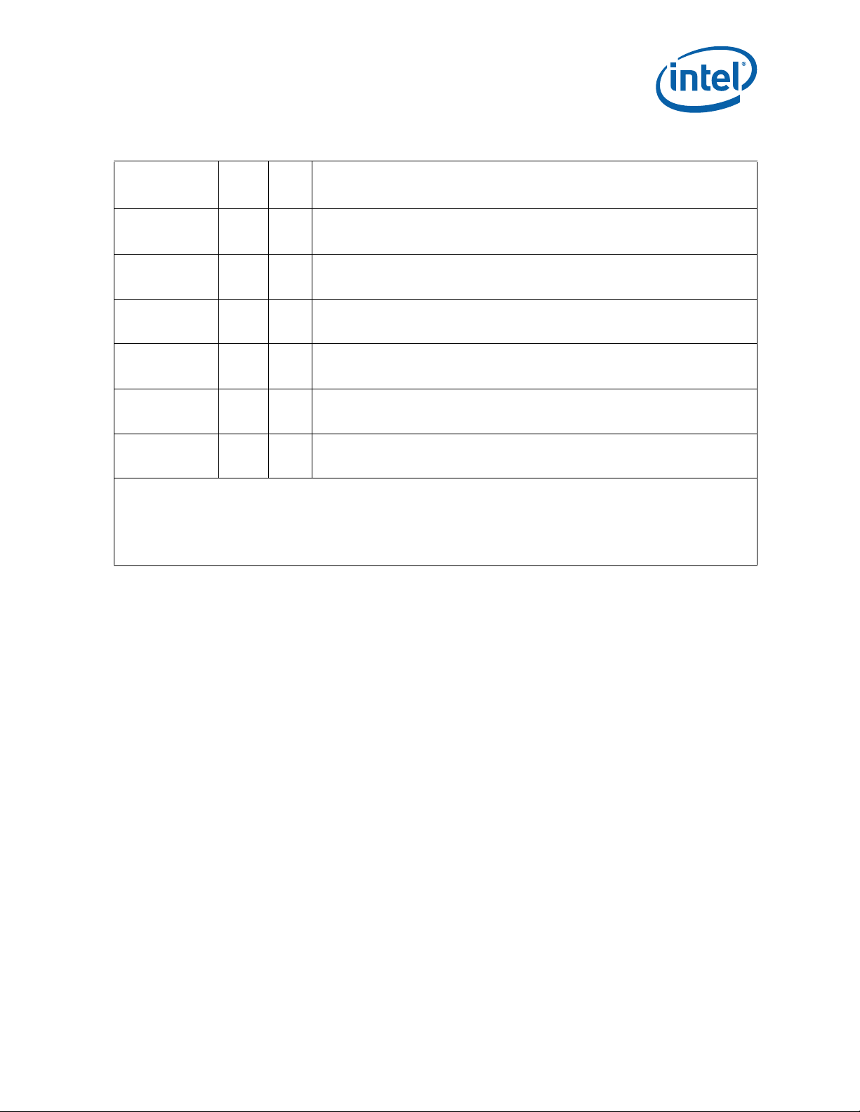
General Hardware Design Considerations—Intel
Network Processors
®
IXP45X and Intel® IXP46X Product Line of
Table 18. High-Speed, Serial Interface 1
Name
Input
Output
Pull
Up
Down
Recommendations
Transmit frame.
HSS_TXFRAME1 I/O Yes
When this interface/signal is enabled and is not being used in a system design, the
interface/signal should be pulled high with a 10-KΩ resistor.
Transmit data out. Open Drain output.
HSS_TXDATA1 OD Yes
When this interface/signal is enabled and is either used or not used in a system design,
the interface/signal should be pulled high with a 10-KΩ resistor to V
CCP
.
Transmit clock.
HSS_TXCLK1 I/O Yes
When this interface/signal is enabled and is not being used in a system design, the
interface/signal should be pulled high with a 10-KΩ resistor.
Receive frame.
HSS_RXFRAME1 I/O Yes
When this interface/signal is enabled and is not being used in a system design, the
interface/signal should be pulled high with a 10-KΩ resistor.
Receive data input.
HSS_RXDATA1 I Yes
When this interface/signal is enabled and is not being used in a system design, the
interface/signal should be pulled high with a 10-KΩ resistor.
Recei ve clock.
HSS_RXCLK1 I/O Yes
Notes:
1. Features disabled/enabled by Soft Fuse must be done during the boot-up sequence. A feature cannot be enabled after
being disabled without asserting a system reset.
2. Features disabled by a specific part number, do not require pull-ups or pull-downs. Therefore, all pins can be left
unconnected.
3. Features enabled by a specific part number — and required to be Soft Fuse-disab led , as s tated in Note 1 — only req uire
When this interface/signal is enabled and is not being used in a system design, the
interface/signal should be pulled high with a 10-KΩ resistor.
pull-ups or pull-downs in the clock-input signals.
February 2007 HDD
Document Number: 305261; Revision: 004 45
Intel® IXP45X and Intel® IXP46X Product Line of Network Processors
Page 46

Intel® IXP45X and Intel® IXP46X Product Line of Network Processors—General Hardware
3.10.2 Device Connection
Figure 14 shows a typical interface between the IXP45X/IXP46X product line and a
SLIC CODEC, via the SSP and HSS ports, and a couple of GPIO signals.
Figure 14. HSS Interface Example
Design Considerations
Intel®IXP46X
Product Line of
Network Processors
GPIO_0
GPIO_1
SSP_EXTCLK
SSP_SCLK
SSP_SFRM
SSP_TXD
SSP_RXD
SSP Interface
HSS_TX_FRAME0
HSS_TXDATA0
HSS_TXCLK0
HSS_RXFRAME0
HSS_RXDATA0
HSS_RXCLK0
HSS_TX_FRAME1
Unused
HSS
HSS_TXDATA1
HSS_TXCLK1
HSS_RXFRAME1
HSS_RXDATA1
HSS_RXCLK1
HSS Interface
External Oscillator
Vccp (3.3 V)
10 KΩ
Vccp (3.3 V)
10 KΩ
10 KΩ
10 KΩ
10 KΩ
Clock derived internally
from 3.6864 MHz
or external oscilator
33 MHz
Clock derived from
SLIC/CO DEC
or external oscilator
512 KHz to
8.192 MHz
Vccp (3.3 V)
10 KΩ
10 KΩ
Vccp (3.3 V)
RESET_N
CLK
CS_N
D I
DO
DTX
FSYNC
RXD
PCLK
SLIC CODEC
INT_N
10 KΩ
AFE
RJ11
B4108-003
3.11 SSP Interface
The IXP45X/IXP46X network processors have a Synchronous Serial Peripheral Interface
(SSP) module. Its primary function is to provide connectivity between the Intel XScale
processor and an external SSP interface.
The SSP module supports National Microwire*, Texas Instruments* synchronous serial
protocol (SSP), and Motorola* serial peripheral interface (SPI).
The clock rate can be selected from an internal, 3.6864-MHz source or external source
fed at input pin SSP_EXTCLK. The clock can then be divided down anywhere from
7.2 KHz to 1.84 MHz by setting bits 15:08 in Control Register 0. For more information,
see the SSP configuration registers in the Intel
Line of Network Processors Developer’s Manual.
®
IXP45X and Intel® IXP46X Product Line of Network Processors
Intel
HDD February 2007
46 Document Number: 305261; Revision: 004
®
IXP45X and Intel® IXP46X Product
Page 47

General Hardware Design Considerations—Intel
Network Processors
®
IXP45X and Intel® IXP46X Product Line of
3.11.1 Signal Interface
Table 19. Synchronous Serial Peripheral Port Interface
Name
SSP_SCLK O No Serial bit clock.
SSP_SFRM O No Serial frame indicator.
SSP_TXD O No Transmit data (serial data out).
SSP_RXD I Yes
SSP_EXTCLK I Yes
Input/
Output
Pull
Up/
Down
Receive data (serial data in).
Should be pulled high through a 10-KΩ resistor when not being utilized in the system.
External clock input.
Should be pulled high through a 10-KΩ resistor when not being utilized in the system.
Recommendations
3.11.2 Device Connection
There are a number of devices available that can interface to SSP or SPI ports, these
can range from RTC (Real-Time Clock), LCD (Liquid Crystal Displays), Digital Thermal
Sensor to Flash memory devices.
One of the most common usage for SSP or SPI port, is serial flash code storage. Serial
flash devices can be used to store board revision, serial numbers, or assembly
information. Figure 15 provides an example of a Serial Flash device interface to the
SSP port in the IXP45X/IXP46X network processors. For an additional example of SPI
interface, refer to Figure 14, in which a SLIC is connected to the SSP and HSS ports.
Figure 15. Serial Flash and SSP Port (SPI) Interface Example
Intel® IXP46X
Product Line
Netw o rk P rocessors
SSP_SCLK
SSP_SFRM
SSP_TXD
SSP_RXD
SSP_EXTCLK
SSP Interface
SPI Flash
CLK
CS_N
D I
DO
7.2 KHz
to 3.6864 MHz
External Oscillator
B4109-001
February 2007 HDD
Document Number: 305261; Revision: 004 47
Intel® IXP45X and Intel® IXP46X Product Line of Network Processors
Page 48

Intel® IXP45X and Intel® IXP46X Product Line of Network Processors—General Hardware
3.12 PCI Interface
The PCI Controller of the IXP45X/IXP46X network processors is an industry-standard,
32-bit interface, high-performance bus that operates at either 33 or 66 MHz (PCI Local
Bus Specification, Rev. 2.2).
The PCI Controller supports operation as a PCI host and implements a PCI arbiter for a
system containing up to four external PCI devices.
As indicated in Figure 16, a PCI transparent bridge is needed to support Compact PCI.
General PCI routing guidelines can be found in Section 6.2, “Topology” on page 71. For
more detailed information, see the PCI Local Bus Specification, Rev. 2.2.
3.12.1 Signal Interface
Table 20. PCI Controller (Sheet 1 of 2)
Design Considerations
Name
PCI_AD[31:0] I/O Yes
PCI_CBE_N[3:0] I/O Yes
PCI_PAR I/O Yes
PCI_FRAME_N I/O Yes
PCI_TRDY_N I/O Yes
PCI_IRDY_N I/O Yes
PCI_STOP_N I/O Yes
PCI_PERR_N I/O Yes
PCI_SERR_N I/O Yes
PCI_DEVSEL_N I/O Yes
Notes:
1. Features disabled/enabled by Soft Fuse must be done during the boot-up sequence. A feature cannot be enabled after
2. Features disabled by a specific part number, do not require pull-ups or pull-downs. Therefore, all pins can be left
3. Features enabled by a specific part number — and required to be Soft Fuse-disabled, as stated in Note 1 — only require
being disabled without asserting a system reset.
unconnected.
pull-ups or pull-downs in the clock-input signals.
Input/
Outpu
Pull
Up/
t
Down
PCI Address/Data bus.
When this interface/signal is enabled and is not being used in a system design, the interface/
signal should be pulled high with a 10-KΩ resistor.
PCI Command/Byte Enables.
When this interface/signal is enabled and is not being used in a system design, the interface/
signal should be pulled high with a 10-KΩ resistor.
PCI Parity.
When this interface/signal is enabled and is not being used in a system design, the interface/
signal should be pulled high with a 10-KΩ resistor.
PCI Cycle Frame.
When this interface/signal is enabled and is either being used or n ot bein g u sed in a system
design, the interface/signal should be pulled high with a 10-KΩ resistor.
PCI Target Ready.
When this interface/signal is enabled and is either being used or not being used in a system
design, the interface/signal should be pulled high with a 10-KΩ resistor.
Initiator Ready.
When this interface/signal is enabled and is either being used or n ot bein g u sed in a system
design, the interface/signal should be pulled high with a 10-KΩ resistor.
Stop.
When this interface/signal is enabled and is either being used or n ot bein g u sed in a system
design, the interface/signal should be pulled high with a 10-KΩ resistor.
Parity Error.
When this interface/signal is enabled and is either being used or n ot bein g u sed in a system
design, the interface/signal should be pulled high with a 10-KΩ resistor.
System Error.
When this interface/signal is enabled and is either being used or n ot bein g u sed in a system
design, the interface/signal should be pulled high with a 10-KΩ resistor.
Device Select:
When this interface/signal is enabled and is either being used or n ot bein g u sed in a system
design, the interface/signal should be pulled high with a 10-KΩ resistor.
Recommendations
®
IXP45X and Intel® IXP46X Product Line of Network Processors
Intel
HDD February 2007
48 Document Number: 305261; Revision: 004
Page 49

General Hardware Design Considerations—Intel
Network Processors
®
IXP45X and Intel® IXP46X Product Line of
Table 20. PCI Controller (Sheet 2 of 2)
Name
PCI_IDSEL I Yes
PCI_REQ_N[3:1] I Yes
PCI_REQ_N[0] I/O Yes
PCI_GNT_N[3:1] O No Arbitration Grant.
PCI_GNT_N[0] I/O Yes
PCI_INTA_N O/D Yes
PCI_CLKIN I Yes
Notes:
1. Features disabled/enabled by Soft Fuse must be done during the boot-up sequence. A feature cannot be enabled after
being disabled without asserting a system reset.
2. Features disabled by a specific part number, do not require pull-ups or pull-downs. Therefore, all pins can be left
unconnected.
3. Features enabled by a specific part number — and required to be Soft Fuse-disabled, as stated in Note 1 — only require
pull-ups or pull-downs in the clock-input signals.
Input/
Outpu
Pull
Up/
Down
t
Initialization Device Select.
When this interface/signal is enabled and is not being used in a system design, the interface/
signal should be pulled high with a 10-KΩ resistor.
Arbitration Request.
When this interface/signal is enabled and is not being used in a system design, the interface/
signal should be pulled high with a 10-KΩ resistor.
Arbitration Request:
When this interface/signal is enabled and is not being used in a system design, the interface/
signal should be pulled high with a 10-KΩ resistor.
Arbitration Grant.
When this interface/signal is enabled and is not being used in a system design, the interface/
signal should be pulled high with a 10-KΩ resistor.
Interrupt A.
When this interface/signal is enabled and is either used or not used in a system design , the
interface/signal should be pulled high with a 10-KΩ resistor.
Clock input.
When this interface/signal is enabled and is not being used in a system design, the interface/
signal should be pulled high with a 10-KΩ resistor.
Recommendations
3.12.2 PCI Interface Block Diagram
When using the IXP45X/IXP46X network processors in Master mode, the PCI module
can interface to up to four PCI cards (devices) at 33 MHz or two PCI cards at 66 MHz.
The limitation to two cards (devices) at 66 MHz is due to load requirements to maintain
signal integrity at the higher frequency.
The PCI-to-PCI bridge must be used in order to address the PCI requirement not to
exceed one load per PCI connector unless it is through a PCI-to-PCI bridge.
The IDSEL signals on the PCI slots can be connected to one of the PCI_AD lines,
preferable to the higher order address signals. Reset support can be accomplished by
using one of the GPIO pins to generate a reset or through an external decoder of the
Expansion bus.
February 2007 HDD
Document Number: 305261; Revision: 004 49
Intel® IXP45X and Intel® IXP46X Product Line of Network Processors
Page 50

Intel® IXP45X and Intel® IXP46X Product Line of Network Processors—General Hardware
Figure 16. PCI Interface
Intel® IXP46X
Product Line
Network Processo r
Design Considerations
cPCI J1
PCI Interface
PCI Bus
PCI Slots
3.12.3 Supporting 5 V PCI Interface
It is possible to support 5 V PCI devices with the help of voltage logic translators. One
option can be implemented with voltage level translator. The Texas Instruments* family
of FET bus switches CBT devices can be a good solution. The 10-bit SN74CB T3384A has
been proven to work very effectively with the Intel
control and DATA/ADDRESS signals (bidirectional and not) need to be translated before
connecting the 3.3 V to the 5 V logic together . Signals which are not used, do not need
to be translated, simply follow the recommendations described in Table 20.
Figure 17 shows a block diagram of the interface required to perform the conversion.
Ensure that all signals connect to either of the two interfacing logic levels.
Bridge
Transp are n t P CI
®
IXP465 Network Processor. All
Compact PCI Bus
B4110- 001
cPCI J2
T
(Bus Propagation Delay) is the maximum time for a complete flight. When you
PROP
calculate T
Propagation Delay) of the voltage translator. For details, refer to Section 6.2.
®
IXP45X and Intel® IXP46X Product Line of Network Processors
Intel
HDD February 2007
50 Document Number: 305261; Revision: 004
you must include in your timing calculation the TPD (Time for
PROP,
Page 51

General Hardware Design Considerations—Intel
Network Processors
®
IXP45X and Intel® IXP46X Product Line of
Figure 17. PCI 3.3 V to 5 V Logic Translation Interface
Intel® IXP46X
Product Line
Netw ork Processo r
PCI
Interface
3.12.4 PCI Option Interface
3.3V LOGIC
3.3V LOGIC
3.3V LOGIC
32-Bit BUS
3.3V LOGIC
1K
1K
3.3V L o g i c
PCI Device_ 1
3.3V L o g i c
PCI Device_2
3.3V L o g i c
PCI Device_3
5.0V
74CBT3384A
OE
10-BIT
10-BIT
OE
GND
74CBT3384A
VCC
GND
VCC
4.3 V
2.87K
5.0V LOGIC
5.0V Logic
PCI Device_4
B5197 -01
The IXP45X/IXP46X network processors can be used in a design as a host or as an
option device. This section describes how the IXP45X/IXP46X network processors can
be connected as an option device to obtain proper functionality. There are slight
differences in the hardware interface when designing for option mode. All routing and
board recommendations described in previous sections of this document apply,
however the design must use the device pin connections listed in Table 21.
Table 21. PCI Host/Option Interface Pin Description (Sheet 1 of 3)
Host
Name
PCI_AD[31:0] I/O
PCI_CBE_N[3:0] I/O
PCI_PAR I/O
PCI_FRAME_N I/O
February 2007 HDD
Document Number: 305261; Revision: 004 51
Input
Outpu
t
Device-Pin Connection
All address/data signals need to be
connected between the two devices.
Connect signals to same pins between
the two devices.
Connect signal to same pin between
the two devices.
Connect signal to same pin between
the two devices.
Connect a 10-KΩ pull-up resistor.
Intel® IXP45X and Intel® IXP46X Product Line of Network Processors
Option
Input
Outpu
t
I/O PCI Address/Data bus
I/O PCI C ommand/Byte Enables
I/O PCI Parity
I/O PCI Cycle Frame
Description
Page 52

Intel® IXP45X and Intel® IXP46X Product Line of Network Processors—General Hardware
Table 21. PCI Host/Option Interface Pin Description (Sheet 2 of 3)
Design Considerations
Host
Name
PCI_TRDY_N I/O
PCI_IRDY_N I/O
PCI_STOP_N I/O
PCI_PERR_N I/O
PCI_SERR_N I/O
PCI_DEVSEL_N I/O
PCI_IDSEL I
PCI_REQ_N[3:1] I
PCI_REQ_N[0] I
PCI_GNT_N[3:1] O
PCI_GNT_N[0] O
Input
Outpu
Device-Pin Connection
t
Connect signal to same pin between
the two devices.
Connect a 10-KΩ pull-up resistor.
Connect signal to same pin between
the two devices.
Connect a 10-KΩ pull-up resistor.
Connect signal to same pin between
the two devices.
Connect a 10-KΩ pull-up resistor.
Connect signal to same pin between
the two devices.
Connect a 10-KΩ pull-up resistor.
Connect signal to same pin between
the two devices.
Connect a 10-KΩ pull-up resistor.
Connect signal to same pin between
the two devices.
Connect a 10-KΩ pull-up resistor.
Connect one of the higher order PCI
address signals to the Device.
Connect a 10K pull-up resistor to the
Host.
From the Option device, connect output
signal PCI_REQ_N[0] to one of the
PCI_REQ_N[3:0] inputs to the Host.
Note: the PCI_REQ_N[n] must
correspond to the PCI_GNT_N[n],
where “n” must be the same number in
the square bracket.
From the Option device, connect output
PCI_REQ_N[0] to one of the
PCI_REQ_N[3:0] inputs to the Host.
Note: the PCI_REQ_N[n] must
correspond to the PCI_GNT_N[n],
where “n” must be the same number in
the square bracket.
Connect one of the Host outputs
PCI_GNT_N[3:0] to PCI_GNT_N[0]
input to the Option.
Note: the PCI_GNT_N[n] must
correspond to the PCI_GNT_N[n],
where “n” must be the same number in
the square bracket.
Connect one of the Host outputs
PCI_GNT_N[3:0] to PCI_GNT_N[0]
input to the Option.
Note: the PCI_GNT_N[n] must
correspond to the PCI_GNT_N[n],
where “n” must be the same number in
the square bracket.
Option
Input
Outpu
t
I/O PCI Target Ready
I/O Initiator Ready
I/O Stop
I/O Parity Error
I/O System Error
I/O Device Select
I Initialization Device Select
Arbitration Request
On the Option device, these signals are not
used, they should be pulled high with a 10-KΩ
resistor .
I
Note: The PCI_REQ_N[n] must correspond
Arbitration Request
On the Option device, this signal is an output
and must be connected to one of the
PCI_REQ_N[3:0] inputs to the Host.
O
Note: The PCI_REQ_N[n] must correspond
Arbitration Grant
On the Option device, these signals are not
O
used, they should be pulled high with a 10-KΩ
resistor.
Arbitration Grant
On the Option device, this signal is an input
and must be connected to one of the
PCI_GNT_N[3:0] outputs of the Host.
I
Note: The PCI_REQ_N[n] must correspond
Description
to the PCI_GNT_N[n], where “n” must
be the same number in the square
bracket.
to the PCI_GNT_N[n], where “n” must
be the same number in the square
bracket.
to the PCI_GNT_N[n], where “n” must
be the same number in the square
bracket.
®
IXP45X and Intel® IXP46X Product Line of Network Processors
Intel
HDD February 2007
52 Document Number: 305261; Revision: 004
Page 53

General Hardware Design Considerations—Intel
Network Processors
®
IXP45X and Intel® IXP46X Product Line of
Table 21. PCI Host/Option Interface Pin Description (Sheet 3 of 3)
Host
Name
PCI_INTA_N O/D
PCI_CLKIN I
Input
Outpu
t
Connect PCI_INTA_N output from the
Option to one of the GPIO input signals
of the Host. The GPIO signal at the
Host must be configure as an input
interrupt level sensitive.
Clock must be connected to both
devices. Trace lengths must be
matched. Use point to point clock
distribution.
3.12.5 Design Notes
• The IXP45X/IXP46X network processors do not support the 5 V PCI signal interface
by itself. Only the 3.3 V signal interface is supported without signal level
conversion, however, it is possible to interface to 5 V logic when using a voltage
level converter. See Figure 17 for details.
•The PCI Local Bus Specification, Rev. 2.2 requires that the bus is always “parked”,
as some device is always driving the AD lines. There is need to use pull-ups on
these signals. The specification states that the following control lines should be
pulled up:
— FRAME# — TRDY# — IRDY# — DEVSEL#
—STOP# —SERR# —PERR# —LOCK#
—INTA# —INTB# —INTC# —INTD#
Device-Pin Connection
Option
Input
Outpu
t
Interrupt A
This interrupt is generated from the Option to
O/D
one of the GPIO inputs to the Host.
On the Host this signal is not used, it should
be pulled high with a 10-KΩ resistor.
I Clock input
Description
• The processors’ GPIO pins can be used by PCI devices on PCI slots to request an
interrupt from the processors’ PCI controller.
• PCI_INTA_N is used to request interrupts to external PCI Masters. This signal is an
open collector and requires a pull-up resistor.
3.13 JTAG Interface
JTAG is the popular name for IEEE standards 1149.1-1990 and 1149.1a-1993, IEEE
Standard Test Access Port and Boundary-Scan Architecture, which provides support
for:
• Board-level boundary-scan connectivity testing
• Connection to software debugging tools through the JTAG interface
• In-system programming of programmable memory and logic devices on the PCB
The interface is controlled through five dedicated test access port (TAP) pins: TDI, TMS,
TCK, nTRST, and TDO, as described in the IEEE 1149.1 standard. The boundary-scan
test-logic elements include the TAP pins, TAP controller, instruction register, boundaryscan register, bypass register, device identification register, and data-specific registers.
These are described in the Intel
Processors Developer’s Manual.
The IXP45X/IXP46X network processors may be controlled during debug through a
JTAG interface to the processor, the debug tools such as the Macraigor* Raven*, EPI*
Majic*, Wind River Systems* visionPROBE* / visionICE* or various other JTAG tools
plug into the JTAG interface through a connector.
®
IXP45X and Intel® IXP46X Product Line of Network
February 2007 HDD
Document Number: 305261; Revision: 004 53
Intel® IXP45X and Intel® IXP46X Product Line of Network Processors
Page 54
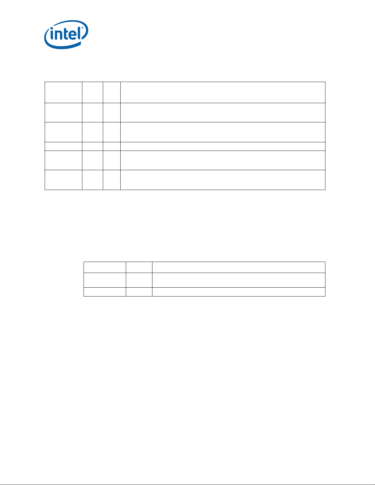
Intel® IXP45X and Intel® IXP46X Product Line of Network Processors—General Hardware
3.13.1 Signal Interface
Table 22. Synchronous Serial Peripheral Port Interface
Design Considerations
Name
JTG_TMS I Yes
JTG_TDI I Yes
JTG_TDO O O Test Output data.
JTG_TRST_N I Yes
JTG_TCK I Yes
Input/
Output
Pull
Up/
Down
Test mode select.
When the JTAG interface is not being used, the signal must be pulled high using a 10-kΩ
resistor.
Test Input data.
When the JTAG interface is not being used, the signal must be pulled high using a 10-kΩ
resistor.
Test Reset.
When the JTAG interface is not being used, the signal must be pulled low using a 10-kΩ
resistor.
Test Clock.
When the JTAG interface is not being used, the signal must be pulled high using a 10-kΩ
resistor.
3.14 Input System Clock
The IXP45X/IXP46X network processors require a 33.33-MHz reference clock to
generate all internal clocks required — including core clock — and the various buses
running internally within the system.
3.14.1 Clock Signals
Table 23. Clock Signals
Recommendations
Name Type* Description
OSC_IN I
OSC_OUT O No connect
Note: For explanations of the
3.14.2 Clock Oscillator
When using an external clock oscillator to supply the 33.33-MHz reference system
clock, connect the clock oscillator output to OSC_IN pin through a series termination of
33 Ω as shown in Figure 18. The series termination helps smooth the rise and fall edges
of the clock and eliminate ringing. Leave the OSC_OUT pin un-connected.
Source must be a clock input of 33.33-MHz.
Use a series termination resistor, 10 Ω to 33 Ω at the source.
Type column abbreviations, see Table 2 on page 17.
®
IXP45X and Intel® IXP46X Product Line of Network Processors
Intel
HDD February 2007
54 Document Number: 305261; Revision: 004
Page 55

General Hardware Design Considerations—Intel
Network Processors
®
IXP45X and Intel® IXP46X Product Line of
3.14.3 Device Connection
Figure 18. Clock Oscillator Interface Example
3.3 V
OSC_IN
OUT
33 Ω
OSC_OUT
Intel® IX P 46X
Product Line of
Netw ork Processors
3.15 Power
To enable low power system design, the IXP45X/IXP46X network processors have
separate power supply domains for the processor core, DDR SDRAM memory, and
input/output peripherals.
Table 24. Power Interface (Sheet 1 of 2)
Name
VCC 1.3 V
VCCP 3.3 V I/O supply voltage.
VCCM 2.5 V DDR memory interface supply voltage.
VSS GND Ground for supply voltages 3.3 V, 2.5 V, and 1.3/1.5 V.
OSC_VCCP 3.3 V
OSC_VSSP GND
OSC_VCC 1.3 V
OSC_VSS GND
Nominal
Voltage
Core supply voltage.
Note: If operating at 667MHz, core supply voltage must be increased to VCC = 1.5 V. For details, see
the Intel
Supply voltage for peripheral (I/O) logic of analog oscillator circuitry.
Require special power filtering circuitry. See the Intel
Network Processors Datasheet.
Ground for peripheral (I/O) logic of analog oscillator circuitry. Used in conjunction with the OSC_VCCP
pins.
Require special power filtering circuitry. See the Intel
Network Processors Datasheet.
Supply voltage for internal logic of the analog oscillator circuitry. Requires special power filtering
circuitry. I f operating at 667 MHz, this voltage must be increased to 1.5 V.
See the Intel
Ground for internal logic of the analog oscillator circuitry. Used in conjunction with the OSC_VCC pins.
Require special power filtering circuitry. See the Intel
Network Processors Datasheet.
®
IXP45X and Intel® IXP46X Product Line of Network Processors Datasheet.
®
IXP45X and Intel® IXP46X Product Line of Network Processors Datasheet.
Description
VDD
10 KΩ
ON
0.01 µF
33.33 MHz
B4111-001
®
IXP45X and Intel® IXP46X Product Line of
®
IXP45X and Intel® IXP46X Product Line of
®
IXP45X and Intel® IXP46X Product Line of
February 2007 HDD
Document Number: 305261; Revision: 004 55
Intel® IXP45X and Intel® IXP46X Product Line of Network Processors
Page 56
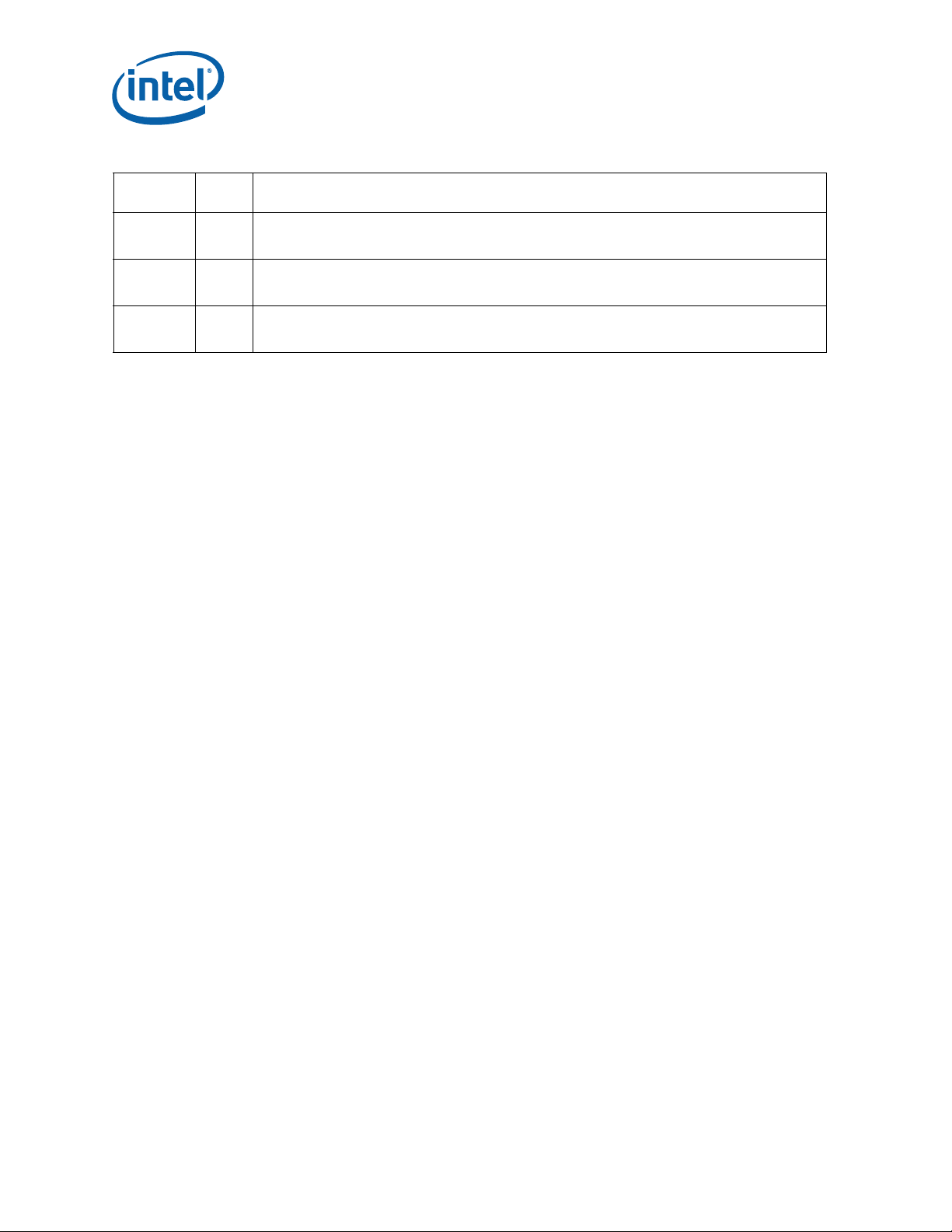
Intel® IXP45X and Intel® IXP46X Product Line of Network Processors—General Hardware
Table 24. Power Interface (Sheet 2 of 2)
Design Considerations
Name
VCCPLL1 1.3 V
VCCPLL2 1.3 V
VCCPLL3 1.3 V
Nominal
Voltage
Supply voltage for internal logic of analog phase lock-loop circuitry. Requires special power filtering
circuitry. If operating at 667 MHz, this voltage must be increased to 1.5 V.
See the Intel
Supply voltage for internal logic of analog phase lock-loop circuitry. Requires special power filtering
circuitry. If operating at 667 MHz, this voltage must be increased to 1.5 V.
See the Intel
Supply voltage for internal logic of analog phase lock-loop circuitry. Requires special power filtering
circuitry. If operating at 667 MHz, this voltage must be increased to 1.5 V.
See the Intel
®
IXP45X and Intel® IXP46X Product Line of Network Processors Datasheet.
®
IXP45X and Intel® IXP46X Product Line of Network Processors Datasheet.
®
IXP45X and Intel® IXP46X Product Line of Network Processors Datasheet.
Description
3.15.1 De-Coupling Capacitance Recommendations
It is common practice to place de-coupling capacitors between the supply voltages and
ground. Placement can be near the input supply pins and ground, with one 100-nF
capacitor per pin. Additional de-coupling capacitors can be place all over the board
every 0.5” to 1.0” . This ensures good return path for currents and reduce power surges
and high-frequency noise.
It is also recommended that 4.7-µF to 10-µF capacitors be placed every 2” to 3”.
3.15.2 VCC De-Coupling
Connect one 100-nF capacitor per each VCC pin. Placement should be as close as
possible to the pin. It is also recommended to place a 4.7-µF capacitor near the device.
Use traces as thick as possible to eliminate voltage drops in the connection.
3.15.3 VCCP De-Coupling
Connect one 100-nF capacitor per each VCCP pin. Placement should be as close as
possible to the pin. It is also recommended to place a 4.7-µF capacitor near the device.
Use traces as thick as possible to eliminate voltage drops in the connection.
3.15.4 VCCM De-Coupling
Connect one 100-nF capacitor per each VCCM pin. Placement should be as close as
possible to the pin. It is also recommended to place a 4.7-µF capacitor near the device.
Use traces as thick as possible to eliminate voltage drops in the connection.
3.15.5 Power Sequence
Power sequence is crucial for proper functioning of the IXP45X/IXP46X network
processors. For a complete description of power sequencing, see the Intel
®
Intel
IXP46X Product Line of Network Processors Datasheet.
3.15.6 Reset Timing
Proper reset timing is also a crucial requirement for proper functioning of the IXP45X/
IXP46X network processors. There are two reset signal PWRON_RESET_N and
RESET_IN_N which required assertion sequence.
®
IXP45X and
®
IXP45X and Intel® IXP46X Product Line of Network Processors
Intel
HDD February 2007
56 Document Number: 305261; Revision: 004
Page 57

General Hardware Design Considerations—Intel
Network Processors
For a complete description of their functionality, see the Intel® IXP45X and Intel®
IXP46X Product Line of Network Processors Datasheet and its section titled “Reset
Timings.” PWRON_RESET_N is used as a Power Good and RESET_IN_N is used for
resetting internal registers.
The IXP45X/IXP46X network processors can be configured at reset de-assertion via
external, pull-down resistors on the address expansion bus signals EX_ADDR[23:21].
For a complete description, see Section 3.3.2, “Reset Configuration Straps” on page 21.
®
IXP45X and Intel® IXP46X Product Line of
February 2007 HDD
Document Number: 305261; Revision: 004 57
Intel® IXP45X and Intel® IXP46X Product Line of Network Processors
Page 58

Intel® IXP45X and Intel® IXP46X Product Line of Network Processors—General Hardware
Design Considerations
®
IXP45X and Intel® IXP46X Product Line of Network Processors
Intel
HDD February 2007
58 Document Number: 305261; Revision: 004
Page 59

General PCB Guide—Intel
®
IXP45X and Intel® IXP46X Product Line of Network Processors
4.0 General PCB Guide
4.1 PCB Overview
Beginning with components selection, this chapter presents general PCB guidelines. In
cases where it is too difficult to adhere to a guideline, engineering judgment must be
used. The methods are listed as simple DOs and DON’Ts.
This chapter does not discuss the functional aspects of any bus, or layout guides for
any interfaced devices.
4.2 General Recommendations
It is recommended that boards based on the IXP45X/IXP46X network processors
employ a PCB stackup yielding a target impedance of 50 Ω ± 10% with 5 mil nominal
trace width. That is, the impedance of the trace when not subjected to the fields
created by changing current in neighboring traces.
When calculating flight times, it is important to consider the minimum and maximum
impedance of a trace based on the switching of neighboring traces. Using wider spaces
between the traces can minimize this trace-to-trace coupling. In addition, these wider
spaces reduce cross-talk and settling time.
4.3 Component Selection
• Do not use components faster than necessary
Clock rise (fall) time should be as slow as possible, as the spectral content of the
waveform decreases
• Use components with output drive strength (slew-rate) controllable if available
• Use SMT components (not through-hole components) as through-hole (leaded)
components have more stub inductance due to the protruding leads.
• Avoid sockets when possible
• Minimize number of connectors
4.4 Component Placement
As shown in Figure 19 on page 60, when placing components, put:
• High-frequency components in the middle
• Medium-frequency around the high-frequency components
• Low-frequency components around the edge of the printed circuit board
February 2007 HDD
Document Number: 305261; Revision: 004 59
Intel® IXP45X and Intel® IXP46X Product Line of Network Processors
Page 60

Intel® IXP45X and Intel® IXP46X Product Line of Network Processors—Category
Figure 19. Component Placement on a PCB
Medium Frequency
High Frequency
Components
Low FrequencyAnalog Circuit
C
O
N
N
E
C
T
O
R
PCB
B2264-01
• Place noisy parts (clock, processor, video, etc.) at least 1.5 – 3 inches away from
the edge of the printed circuit board.
• Do not place noisy components close to internal/external cables
— Any loose cables picks up noise and act as an antenna to radiate that noise
— Be aware of the peak in-rush surge current into the device pins. This surge
current may inject high-frequency switching noise into power planes of the
printed circuit board.
• Place high-current components near the power sources.
• Do not share the same physical components (such as buffers and inverters)
between high-speed and low-speed signals. Use separate parts.
• Place clock drivers and receivers such that clock trace length is minimized.
• Place clock generation circuits near a ground stitch location. Place a localized
ground plane around the clock circuits and connect the localized plane to system
ground plane.
• Install clock circuits directly on the printed circuit board, not on sockets.
• Clock crystals should lie flat against the board to provide better coupling of
electromagnetic fields to the board.
4.5 Stack-U p Sel e ction
Stack-up selection directly affects the trace geometry which, in turn, affects the
characteristic impedance requirement for the printed-circuit board. Additionally, the
“clean,” noise-free-planes design and placement is significantly important as
components run at higher speeds requiring more power.
Considerations include:
• Low-speed, printed-circuit-board construction — for example two-layer boards:
— Advantages:
•Inexpensive
• Manufactured by virtually all printed-c ircuit-board vendors
— Disadvantages:
®
IXP45X and Intel® IXP46X Product Line of Network Processors
Intel
HDD February 2007
60 Document Number: 305261; Revsion: 004
Page 61

General PCB Guide—Intel
• High-speed circuits require multi-layer printed circuit boards:
— Advantages:
— Disadvantages:
• Symmetry is essential to keep the board stack-up symmetric about the center
This minimizes warping
• For best impedance control, have:
— No more than two signal layers between every power/ground plane pair
— No more than one embedded micro-strip layer under the top/bottom layers
• For best noise control, route adjacent layers orthogonally. Avoid layer-to-layer
parallelism.
• Fabrication house must agree on design rules, including:
— Trace width, trace separation
— Drill/via sizes
• The distance between the signal layer and ground (or power) should be minimized
to reduce the loop area enclosed by the return current
— Use 0.7:1 ratio as a minimum.
®
IXP45X and Intel® IXP46X Product Line of Network Processors
• Poor routing density
• Uncontrolled signal trace impedance
• Lack of power/ground planes, resulting in unacceptable cross-talk
• Relatively high-impedance power distribution circuitry, resulting in
noise on the power and ground rails
• Control led-impedance traces
• Low-impedance power distribution
• Higher cost
•More weight
• Manufactured by fewer vendors
For example: 5-mil traces, 7-mil prepreg thickness to adjacent power/ground.
Figure 20 gives an example for a six-layer and eight-layer board. For stripline (signals
between planes), the stackup should be such that the signal line is closer to one of the
planes by a factor of five or more. Then the trace impedance is controlled
predominantly by the distance to the nearest plane.
Figure 20 and Figure 21 illustrate the proposed stackup for the six- and eight-layer
boards.
February 2007 HDD
Document Number: 305261; Revision: 004 61
Intel® IXP45X and Intel® IXP46X Product Line of Network Processors
Page 62

Figure 20. 8-Layer Stackup
Intel® IXP45X and Intel® IXP46X Product Line of Network Processors—Category
Solder (Bottom) Side
Figure 21. 6-Layer Stackup
Solder (Bottom) Side
Component (Top) Side
Data
Data
Data
Data
Data
Data
Component (Top) Side
4.5 mil
5 mil
4.5 mil
7 mil
~40 mil
7 mil
4.5 mil
7 mil
7 mil
4.5 mil
17.8 mil
62 mil
5 mil
62 mil
L1
L2
L3
L4
L5
L6
L7
L8
L1
L2
L3
L4
L5
L6
SIGNAL
POWER
SIGNAL
GND
POWER
Legend
GND
B2244-02
Legend
B2275-02
• Fast and slow transmission line networks must be considered
•PCB-board velocities
•Board FR4 ~ 4.3
• Target impedance of 50 Ω ± 10%
• Trace width: 5 mils
• Signal Layers (1/2 oz. Copper)
• Power Layer (1 oz. Copper)
• Ground (GND) Layer (1 oz. Copper)
®
IXP45X and Intel® IXP46X Product Line of Network Processors
Intel
HDD February 2007
62 Document Number: 305261; Revsion: 004
Page 63

General Layout and Routing Guide—Intel
Processors
®
IXP45X and Intel® IXP46X Product Line of Network
5.0 General Layout and Routing Guide
5.1 Overview
This chapter provides routing and layout guides for hardware and systems based on the
®
Intel
IXP45X and Intel® IXP46X Product Line of Network Processors.
The high-speed clocking required when designing with the processors requires special
attention to signal integrity. In fact, it is highly recommended that the board design be
simulated to determine optimum layout for signal integrity. The information in this
chapter provides guidelines to aid designers with board layout. In cases where it is too
difficult to follow a design rule, engineering judgment must be used.
5.2 General Layout Guidelines
The layout guidelines recommended in this section are based on experience and
knowledge gained from previous designs. Layer stacking varies, depending on design
complexity, however following standard rules helps minimize potential problems
dealing with signal integrity.
The following are well know documented recommendations that helps route a
functional board:
• Providing enough routing layers to comply with minimum and maximum timing
requirements of the IXP45X/IXP46X network processors and other components.
• Connectors, and mounting holes must be placed in a ways that will not interfere
with basic design guidelines in this document.
• Provide uniform impedance throughout the board, specially for high speed areas
such us clocking, DDR-SDRAM, PCI, device bus, etc.
• Place analog, high-voltage, power supply, low-speed, and high-speed devices in
different sections of the board.
• Decoupling capacitors must be placed next to power pins.
• Series termination resistors must be placed close to the source.
• Analog and digital sections of the board must be physically isolated from each
other. No common ground, power planes, and signal traces are allowed to crossisolation zones. Use appropriately sized PCB traces for larger enough to handle
peak current. Keep away from high-speed digital signals.
• Keep stubs as short as possible (preferably, the electrical length of the stub less
than half of the length of the rise time of signal).
• All critical signals should be routed before all other non-critical signals.
• Do not route signals close to the edge of the board, power or ground planes. Route
signal at least 50 to 100 mils away from the edge of the plane.
• Try to match buses to the same trace length and keep them in groups adjacent to
each other, away from other signals.
• Route processor address, data and control signals using a “daisy-chain” topology.
• Minimize number of vias and corners on all high speed signals.
• Do not route under crystals or clock oscillators, clock synthesizers, or magnetic
devices (ferrites, toroids).
• Maintain trace spacing consistent between differential pairs and match trace length.
• Keep differential signals away from long and parallel, high-speed paths, such as
clock signals and data strobe signals.
February 2007 HDD
Document Number: 305261; Revision: 004 63
Intel® IXP45X and Intel® IXP46X Product Line of Network Processors
Page 64

Intel® IXP45X and Intel® IXP46X Product Line of Network Processors—Category
• Do not place high-frequency oscillators and switching network devices close to
sensitive analog circuits.
• Arrange the board so that return currents for high-speed traces never must jump
between planes. Restrict traces to remain on either side of whichever ground plane
they start out nearest. This allows the use of naturally grouped horizontal and
vertical routing layers.
If signals change between layers, the reference voltage changes, as shown in
Figure 22. This creates discontinuity in the path of the signal.
Figure 22. Signal Changing Reference Planes
Driver
GND
PWR
Signal
ByPass Caps
Trace
The design in Figure 22, routes a signal on the top layer, close to GND plane, and
provides a very good return current path. The signal then is routed to the bottom layer,
close to the PWR plane, such that the return currents flows to the ground plane through
bypass caps. Hence the path for the return currents is less inductive than in the
previous case when the signal is routed on the top layer.
5.2.1 General Component Spacing
• Do not place components within 125 mils to the edge of the printed circuit board.
For exact dimensions consult your manufacturing vendor.
• Keep a minimum spacing between via and the solder pad edges > 25mil.
• Position devices that interface with each other close to one another to minimize
trace lengths.
VIAs
Return Current
Signal
Signal
Receiver
B2269-01
®
IXP45X and Intel® IXP46X Product Line of Network Processors
Intel
HDD February 2007
64 Document Number: 305261; Revision: 004
Page 65

General Layout and Routing Guide—Intel
Processors
®
IXP45X and Intel® IXP46X Product Line of Network
Figure 23. Good Design Practice for VIA Hole Placement
25 mils min
25 mils min
25 mils min
B2266-01
Figure 23 and Figure 24 show good and poor design practices for via placement on
surface-mount boards.
Figure 25 shows minimum pad-to-pad clearance for surface-mount passive
components and PGA or BGA components.
Figure 24. Poor Design Practice for VIA Placement
Flush Via min
Potential Bridge min
B2267-01
February 2007 HDD
Document Number: 305261; Revision: 004 65
Intel® IXP45X and Intel® IXP46X Product Line of Network Processors
Page 66

Intel® IXP45X and Intel® IXP46X Product Line of Network Processors—Category
Figure 25. Pad-to-Pad Clearance of Passive Components to a PGA or BGA
PGA or BGA Package
60 mils min
60 mils min 60 mils min
5.2.2 Clock Signal Considerations
• Provide good return current paths for clock traces.
• Keep clock traces away from the edge of the board and any other high-speed
devices or traces.
• Keep clock traces away from analog signals, including voltage reference signals.
• Clock signals should not cross over a split plane.
• Route clock signals in a single, internal layers and eliminate routing in multiple
layers as much as possible.
• Do not route traces or vias under crystals or clock oscillators devices unless there is
a plane between the trace and the component.
• Do not route parallel signal traces directly above or below clock traces unless there
is a ground or at least a power plane separation between those layers.
• Route clock traces with a minimum number of vias.
• Space clock traces away from other signals three times the trace width on each
side.
• Use guard traces when routing on top or bottom layers whenever possible. Guard
traces must be connected to ground.
• Do not daisy-chain, instead use point-to-point clock distribution. Place a series
termination resistor as close as possible to the source.
• Keep traces short to minimize reflections and signal degradation.
• Maintain control impedance for all clock traces, microstrip or stripline.
— Be aware of propagation delays between a microstrip and stripline.
B2268-01
®
IXP45X and Intel® IXP46X Product Line of Network Processors
Intel
HDD February 2007
66 Document Number: 305261; Revision: 004
Page 67

General Layout and Routing Guide—Intel
Processors
®
IXP45X and Intel® IXP46X Product Line of Network
— Calculate capacitive loading of all components and properly compensate with a
series or parallel terminations.
• Measure and match trace lengths for devices that interface with each other and
have their clock derived from the same source.
If traces must be long, treat them as transmission lines. Terminate clock traces to
match trace impedance.
• If there is a power plane, instead of a ground plane, make sure that the power
plane has adequate decoupling to ground, especially near clock drivers and
receivers.
5.2.3 SMII Signal Conside r ations
SMII signals run at 125 MHz, single-ended and require proper trace-routing to achieve
good signal integrity and impedance matching. The following recommendations help
with designs:
• Do not route any of the SMII signals under the IXP45X/IXP46X network processors,
or any other components, unless a ground or power plane isolates the signals.
• Minimize the number of vias to two per trace.
• Keep traces as short as possible and straight, away from other signals.
• Control impedance should maintain to 50 Ω.
• RX signals must have the same length and TX signals must have the same length.
— For the RX group, match the lengths for signals SMII_RX_SYNC,
SMII_RX_DATA, and SMII_RX_CLK.
— For TX group, match lengths for signals SMII_TX_SYNC, SMII_TX_DATA, and
SMII_TX_CLK.
• Avoid sharp corners, using 45° corners instead.
5.2.4 MII Signal Conside rations
MII signals run at 25 MHz which makes them less critical that SMII. But these signals
still require certain routing guide lines.
• Minimize the number of vias to two per trace.
• Keep traces as short as possible and straight, away from other signals.
• Control impedance should maintain to 50 Ω.
• Each group either RX or TX must be length match.
• Avoid sharp corners, using 45° corners instead.
5.2.5 USB Considerations
Follow the schematic sample shown in Section 3.8, “USB Interface” on page 38 and the
recommended schematic interface.
The following are recommendations for routing differential pair signal required to by
the USB interface:
• T races can be routed in tightly cou ple structure with 5mil trace width and 10-mil air
gap, or maintain air gap equal 2X trace width. It is recommended these be handrouted.
• Match trace length for each differential pair.
• Avoid sharp corners, using 45° corners instead.
February 2007 HDD
Document Number: 305261; Revision: 004 67
Intel® IXP45X and Intel® IXP46X Product Line of Network Processors
Page 68

• Wherever possible, use a perfect symmetry within a differential pair.
• Minimize the number vias.
• Avoid routing other signals close by or in parallel to the differential pair,
maintaining no less than 50 mil to any other signal.
• Maintain control impedance for each differential pair to 90 Ω +/- 15 Ω.
• Use high value ferrite beads (100 MHz/60 Ω – 100 MHz/240 Ω).
5.2.6 Cross-Talk
Cross-talk is caused by capacitance and inductance coupling between signals. It is
composed of both backward and forward cross-talk components.
Backward cross-talk creates an induced signal on the network that propagates in the
opposite direction of the aggressor signal. Forward cross-talk creates a signal that
propagates in the same direction as the aggressor signal.
Circuit board analysis software should be used to analyze your board layout for crosstalk problems.
• To effectively route signals on the PCB, signals are grouped (address, data, etc.).
— The space between groups can be 3 w (where w is the width of the traces).
— Space within a group can be just 1 w.
— Space between clock signals or clock to any other signal should be 3 w. The
coupled noise between adjacent traces decreases by the square of the distance
between the adjacent traces.
Intel® IXP45X and Intel® IXP46X Product Line of Network Processors—Category
5.2.7 EMI-Design Considerations
It is strongly recommended that good electromagnetic interference (EMI) design
practices be followed when designing with the IXP45X/IXP46X network processors.
• Information on spread-spectrum clocking is available in Intel® IXP4XX Product Line
of Network Processors and IXC1100 Control Plane Processor: Spread-Spectrum
Clocking to Reduce EMI Application Note.
• Place high-current devices as closely as possible to the power sources.
• Proper termination of signals can reduce reflections, which may emit a highfrequency component that may contribute to more EMI than the original signal
itself.
• Ferrite beads may be used to add high frequency loss to a circuit without
introducing power loss at DC and low frequencies. They are effective when used to
absorb high-frequency oscillations from switching transients or parasitic
resonances within a circuit.
• Keep rise and fall times as slow as possible. Signals with fast rise and fall times
contain many high-frequency harmonics which may radiate significantly.
• A solid ground is essential at the I/O connector to chassis and ground plane.
• Keep the power plane shorter than the ground plane by at least 5x the spacing
between the power and ground planes.
• Stitch together all ground planes around the edge to the board every 100 to
200 mil. This helps reduce EMI radiating out of the board from inner layers.
®
IXP45X and Intel® IXP46X Product Line of Network Processors
Intel
HDD February 2007
68 Document Number: 305261; Revision: 004
Page 69

General Layout and Routing Guide—Intel
Processors
®
IXP45X and Intel® IXP46X Product Line of Network
5.2.8 Trace Impedance
All signal layers require controlled impedance of 50 Ω ±10 % microstrip or stripline
(unless otherwise specified) where appropriate. Selecting the appropriate board stackup to minimize impedance variations is very important.
When calculating flight times, it is important to consider the minimum and maximum
trace impedance based on the switching neighboring traces.
5.2.9 Power and Ground Plane
Power and ground planes should have sufficient de-coupling capacitors to ensure
sustainable current needed for high-speed switching devices. (See Section 3.15.1, “De-
Coupling Capacitance Recommendations” on page 56.)
• It is highly recommended to use sufficient internal power and ground planes.
• Due to the complexity of the IXP45X/IXP46X network processors, there are a
number of power supplies required. It is appropriate to use power islands in the
power plane under the processor, as it would be too expensive to have a power
plane for each power source.
• Power islands must be large enough to include the required power supply
decoupling capacitance, and the necessary connection to the voltage source and
destination.
• Islands can be separated by a minimum of 20-mil air gap.
• Use at least one via per power or ground pin, wherever possible use more vias,
depending on current drawn.
• Use at least one de-coupling capacitor per power pin and place it as close as
possible to the pin.
• Minimize the number of traces routed across the air gaps between power islands.
— Each crossing introduces signal degradation due to the impedance
discontinuity.
— For traces that m ust cross air gaps, route them on the side of the board next to
a ground plane to reduce or eliminate signal degradation caused by crossing
the gap.
— When this is not possible, then route the trace to cross the gap at a right angle
(90°).
February 2007 HDD
Document Number: 305261; Revision: 004 69
Intel® IXP45X and Intel® IXP46X Product Line of Network Processors
Page 70

Intel® IXP45X and Intel® IXP46X Product Line of Network Processors—Category
®
IXP45X and Intel® IXP46X Product Line of Network Processors
Intel
HDD February 2007
70 Document Number: 305261; Revision: 004
Page 71

PCI Interface Design Considerations—Intel
Network Processors
®
IXP45X and Intel® IXP46X Product Line of
6.0 PCI Interface Design Considerations
The Intel® IXP45X and Intel® IXP46X Product Line of Network Processors has a single,
32-bit PCI device module that runs at 33/66 MHz. This chapter describes some basic
guidelines to help design hardware that interfaces with PCI devices.
The PCI module is compatible with the PCI Local Bus Specification, Rev. 2.2. For a
complete functional description and physical requirements, see PCI Local Bus
Specification, Rev. 2.2.
6.1 Electrical Interface
The electrical definition is restricted to 3.3 V signaling environment. The device is not
5 V tolerant. All devices interfacing with the PCI module need to operate at 3.3 V.
6.2 Topology
Interfacing devices need to be connected in a daisy-chain topology. When more than
one device is in the bus, connecting stubs need to be kept as short as possible.
There is a limitation to the number of devices connected to the internal arbiter. If more
than four devices are required to be connected, an external arbiter is required.
The system time budget must be satisfied for 66 MHz and 33 MHz cycles. It is expected
that if the timing budget for 66 MHz clock cycles is satisfied, then the 33 MHz cycles
also work. The following equation and timing parameters need to be met when routing
a board that either interfaces to a single PCI device or up to four devices as shown in
Figure 26.
T
≥ T
CYC
VAL
+T
PROP
+ T
SKEW
+ T
SU
where:
T
= Valid Output Delay
VAL
T
= Bus Propagation Delay (maximum time for complete flight)
PROP
T
= Total Clock Skew
SKEW
T
= Input Setup Time
SU
@33 MHz T
@66 MHz T
= 30 nSec T
CYC
= 15 nSec T
CYC
= 11 nSec T
VAL
= 6 nSec T
VAL
= 10 nSec T
PROP
= 5 nSec T
PROP
= 2 nSec TSU = 7 nSec
SKEW
= 1 nSec TSU = 3 nSec
SKEW
When defining the maximum length of segments A and B as shown in Figure 26, the
calculation must:
• Include an additional trace length segment from the PCI connector to the input
device within the expansion PCI card.
• Assume the segment to be 1.5 inch.
• Use trace propagation delay of 150 to 190 ps/in as specified by the PCI standard.
February 2007 HDD
Document Number: 305261, Revision: 004 71
Intel® IXP45X and Intel® IXP46X Product Line of Network Processors
Page 72

Intel® IXP45X and Intel® IXP46X Product Line of Network Processors—PCI Interface Design
Figure 26. PCI Address/Data Topology
Considerations
Intel® IXP46X
Product Line
PCI Slot
Network Processor
A
Table 25. PCI Address/Data Routing Guidelines
Parameter Routing Guidelines
Signal Group PCI Address/Data
Topology Daisy Chain
Reference Plane Ground
Characteristic Trace Impedance 55 Ω ±10%
Nominal Trace Width 5 mils
Nominal Trace Separation 10 mils
Spacing to Other Groups 20 mils
Limit the number of VIAS to 10 per Signal 10
PCI Slot PCI Sl o t PCI Slot
BBB
B5196 - 01
6.3 Clock Distribution
In order to meet timing and avoid clock overloading, it is recommended to use pointto-point clock distribution as shown in Figure 27.
Clock skew between interfacing devices is very critical and must be met. The maximum
skew must be measured between any two components. If designing a motherboard,
the skew must be measured to the expansion card device and not to the PCI connector.
Ensure that clock skew between all devices does not exceed the values in Section 6.2.
®
IXP45X and Intel® IXP46X Product Line of Network Processors
Intel
HDD February 2007
72 Document Number: 305261, Revision: 004
Page 73

PCI Interface Design Considerations—Intel
Network Processors
Figure 27. PCI Clock Topology
®
IXP45X and Intel® IXP46X Product Line of
PCI Devices
33/66 MHz
Table 26. PCI Clock Routing Guidelines
Signal Group PCI Clock
Reference Plane Ground
Characteristic Trace Impedance 55 Ω ±10%
Nominal Trace Width 5 mils
Nominal Trace Separation 10 mils
Spacing to Other Groups 20 mils
Trace length A Maximum 300 mils
Trace length B
Maximum VIAS 6
Driver
Parameter Routing Guidelines
Topology Point-to-Point
Resistor Rs 22 Ω ±10%
Clock
A
B
Rs
A
B
Rs
A
B
Rs
There is no limit as long as the trace
length is maintained for each clock and
that maximum clock skew is not violated.
Intel® IXP46X
Product Line
Network
Processor
B4114-02
6.3.1 Trace Length Limits
Maximum trace lengths can be calculated for specific speeds at which the bus is
intended to run. Typically, PCI boards with devices that can support up to 66 MHz are
designed to function at up to 66 MHz, even if the design is originally intended to run at
33 MHz. This way , if design requirements change to 66 MHz, then timing is met at the
higher frequency. In this case, the only additional requirement is to change the clock
speed and the expansion bus initial strapping at the EX_ADDR[4] signal. If you are
designing your board for 66 MHz and intend it to operate at 33 MHz, ensure that timing
equations in Section 6.2 are met at 33 MHz and 66 MHz.
February 2007 HDD
Document Number: 305261, Revision: 004 73
Intel® IXP45X and Intel® IXP46X Product Line of Network Processors
Page 74

Intel® IXP45X and Intel® IXP46X Product Line of Network Processors—PCI Interface Design
Considerations
The limitations of the maximum trace length can be calculated with the equations
shown in Section 6.2. Solve for T
This is a straight-forward calculation, but very critical to meet timing. It is
recommended to keep the trace lengths as short as possible and not to exceed T
and use it to calculate the maximum trace length.
PROP
PROP
.
Note: For acceptable signal integrity at up to 66 MHz, it is very important to design the PCB
board with controller impedance in the range of 55 Ω ±10%
.
6.3.2 Routing Guidelines
It is recommended to route signals with respect to an adjacent ground plane. If routing
signals over power planes, ensure that the signals are referenced to a single power
plane voltage level and not multiple levels. For example, you can route signals over a
3.3 V plane or a 5 V plane, but do not route the same signal over both planes. If signals
are routed over split planes, you must connect the splitting planes with 0.01 µF, highspeed capacitors near the signal crossing the split. The capacitors should be placed no
more than 0.25 inches from the point at which the signals cross the split.
This manual does not repeat all the guidelines that are already stated in the PCI Local
Bus Specification, Rev. 2.2, instead you should refer to the specification when
designing either a motherboard or an expansion card.
6.3.3 Signal Loading
Shared PCI signals must be limited to one load on each of the PCI slots. Any violation of
expansion board or add-on device trace length or loading limits compromises systemsignal integrity.
®
IXP45X and Intel® IXP46X Product Line of Network Processors
Intel
HDD February 2007
74 Document Number: 305261, Revision: 004
Page 75

DDR-SDRAM—Intel
®
IXP45X and Intel® IXP46X Product Line of Network Processors
7.0 DDR-SDRAM
7.1 Introduction
This document is intended to be used as a guide for routing DDR, based on the Intel®
IXDP465 Development Platform. It contains routing guidelines and simulation results
for using x16 Thin Small Outline Package (TSOP) memory devices soldered onto the
processor module.
As shown in Figure 28, the Intel
Processors support two banks of 32-bit wide non-Error Correcting Code (non-ECC) or
40-bit wide (ECC) DDR-266 memory with the ability for single-bit error correction or
multi-bit error detection (ECC). The IXP45X/IXP46X network processors support unbuffered DRAM only in densities of 128/256/512 Mbit or 1 Gbit. Table 27 lists the signal
groups used for the DDR interface.
In this document, the term IXP45X/IXP46X product line refers to both the IXP46X
network processors (with DDR ECC) and IXP45X network processors (without DDR
ECC).
Table 27. DDR Signal Groups
®
IXP45X and Intel® IXP46X Product Line of Network
Group Signal Name Description
Clocks
Data
Control
Command
DDRI_CK[2:0] DDR-SDRAM Differential Clocks 0
DDRI_CK_N[2:0] DDR-SDRAM Inverted Differential Clocks 0
DDRI_CB[7:0] ECC Data 8
DDRI_DQ[31:0] Da ta Bus 32
DDRI_DQS[4:0] Data Strobes 5
DDRI_DM[4:0] Data Mask 5
DDRI_CKE[1:0] Clock Enable - one per bank 2
DDRI_CS_N[1:0] Chip Select - one per bank 2
DDRI_MA[13:0] Address Bus 14
DDRI_BA[1:0] Bank Select 2
DDRI_RAS_N Row Address Select 1
DDRI_CAS_N Column Address Select 1
DDRI_WE_N Write Enable 1
Total 73
No of Single
Ended Signals
February 2007 HDD
Document Number: 305261, Revision: 004 75
Intel® IXP45X and Intel® IXP46X Product Line of Network Processors
Page 76

Intel® IXP45X and Intel® IXP46X Product Line of Network Processors—Category
Figure 28. Processor-DDR Interface
DDRI_DQ[31:0]
DDRI_MA[13:0]
DDRI_CK[2:0]
DDRI_CK_N[2:0]
DDRI_CKE[1:0]
DDRI_CS_N[1:0]
DDRI_BA[1:0]
DDRI_CB[7:0]
Product Line of Net work Pr oce ssor s
DDRI_DM[4:0]
®
Intel
DDRI_DQS[4:0]
DATA[31:0]
ADDRESS[13:0]
CLOCK[2:0], CLOCK#[2:0]
CLOCK EN AB LE[1:0]
CHIP SELECT#[1:0]
BANK SE LECT[1:0]
ECC DATA[7:0]
DATA MASK [4:0]
DATA STROBE[4:0]
DQ[31:0]
A[13:0]
CK[2:0]
CK#[2:0]
CKE[1:0]
D DR SDRAM
CS#[1:0]
BA[1:0]
DQ[7:0]
DM[4:0]
DQS[4:0]
DDRI_WE_N
DDRI_RAS_N
DDRI_CAS_N
WRITE#, RAS#, CAS#
WE#
RAS#
CAS#
B3986-001
Table 28 provides a list of supported memory configurations that can be implemented
for one or two banks. Notice that depending on the number of devices used, loading of
the driving signals is affected. The most critical signal affected by the loading is the
DDRI_CK (clock output). This signal has a very strict timing requirement defined in the
JEDEC standard, therefore signal integrity of this signal is a must. The following table
shows how to assign the number of devices per clock line for the various configuration.
It also suggest to use a DDR SSTL zero delay clock driver when more than two devices
per clock line are connected. From Table 28, any time the word “driver” appears, it is
meant to let designers know that for that particular configuration, a clock driver is
required. One recommended clock driver can be the Pericom PI6CV855 or a similar
device. The Pericom device is highly used in DIMM memory modules that required to
deliver clocks to many devices in a single module.
The best approach is to minimize the number of devices used to get the target total
memory size required by design.
®
IXP45X and Intel® IXP46X Product Line of Network Processors
Intel
HDD February 2007
76 Document Number: 305261, Revision: 004
Page 77

DDR-SDRAM—Intel
Besides assigning clock signals (DDRI_CK and DDRI_CK_N) to the memory devices,
there are two more requirements, one implemented in hardware (termination) and the
other implemented in software (configuration), these requirements are explained as
follow:
Note that when simulating, the IBIS model representation of signals DDRI_CK[2:0] and
DDRI_CK_N[2:0] has been created for the new Rcomp settings described in Section
7.1.6, “Resistive Compensation Register (Rcomp)” on page 88
®
IXP45X and Intel® IXP46X Product Line of Network Processors
• It is recommended to properly terminate the clock output signals by the Thevenin
terminations scheme as shown in Figure 37. Simulation is recommended for cases
that required deviation from the recommended topology, which include series
termination and trace impedance.
• It is required to tune the drive strength of the clock driver to properly drive clocks
out to loads of one or two memory devices, terminated with Thevenins termination
scheme. Follow the recommendations described in Section 7.1.6, “Resistive
Compensation Register (Rcomp)” on page 88.
February 2007 HDD
Document Number: 305261, Revision: 004 77
Intel® IXP45X and Intel® IXP46X Product Line of Network Processors
Page 78

Intel® IXP45X and Intel® IXP46X Product Line of Network Processors—Category
Table 28. Supported Memory Configurations
DDR
Device
Density
128 Mbit x8 4 2,2 5 2,2,1 1 64 Mbyte
128 Mbit x8 8 Driver 10 Driver 2 128 Mbyte
128 Mbit x16 2 1,1 3 1,1,1 1 32 Mbyte
128 Mbit x16 4 2,2 6 2,2,2 2 64 Mbyte
256 Mbit x8 4 2,2 5 2,2,1 1 128 Mbyte
256 Mbit x8 8 Driver 10 Driver 2 256 Mbyte
256 Mbit x16 2 1,1 3 1,1,1 1 64 Mbyte
256 Mbit x16 4 2,2 6 2,2,2 2 128 Mbyte
512 Mbit x8 4 2,2 5 2,2,1 1 256 Mbyte
512 Mbit x8 8 Driver 10 Driver 2 512 Mbyte
512 Mbit x16 2 1,1 3 1,1,1 1 128 Mbyte
512 Mbit x16 4 2,2 6 2,2,2 2 256 Mbyte
1 Gbit x8 4 2,2 5 2,2,1 1 512 Mbyte
1 Gbit x8 8 Driver 10 Driver 2 1 Gbyte
1 Gbit x16 2 1,1 3 1,1,1 1 256 Mbyte
1 Gbit x16 4 2,2 6 2,2,2 2 512 Mbyte
Device
Width
Number of
DDR Devices
(non-ECC)
Devices
per
Clock
Number of
DDR Devices
(ECC)
Devices
per
Clock
Number
of Banks
Total
Memory Size
Figure 29 shows the DDR memory interface of the IXP45X/IXP46X network processors
using x16 devices with Error Correcting Code (ECC). Bank 0 is represented by DDR
devices 1, 3, and 5. Bank 1 is represented by DDR devices 2, 4, and 6. Unused data
inputs on the ECC devices (5 and 6) are pulled to ground through 10-KΩ resistors.
The VTT signal termination used for all signals, except clocks, is a series 60.4- Ω resistor
to a 1.25-V DC power supply designed for DDR memory termination. The appropriate
value for termination resistance should be verified through simulation for the specific
topology as shown in “Simulation Results” on page 90. The supply chosen for this
application was the TPS54672 from Texas Instruments*.
The DDRI_RCVENOUT_N signal must be connected to the DDRI_RCVENIN_N signal
with a trace which is propagation delay length matched to the average delay of the
clock (DDRI_CK[2:0]) plus data (DDRI_DQ[31:0]). A series terminating resistor (Rs)
should be used to control overshoot and undershoot, as shown in Figure 49 on
page 105.
A resistance value in the 25- to 50-Ω range should be used as it adds minimal
propagation delay to the signal without adversely varying from the CLK plus DQ
propagation delay average. The appropriate v alue for termination resistance should be
verified through simulation for the specific topology.
The DDRI_RCOMP signal must be terminated through a 20-Ω, 1%, 0.1-W resistor
(R
adjustments.
®
IXP45X and Intel® IXP46X Product Line of Network Processors
Intel
HDD February 2007
78 Document Number: 305261, Revision: 004
) to ground. This allows the DDR controller to make temperature and process
comp
Page 79

DDR-SDRAM—Intel
®
IXP45X and Intel® IXP46X Product Line of Network Processors
Figure 29. Processor-DDR Interface: x16 Devices with ECC
GND
DDRI_RCVENOUT_N
R
s
DDRI_RCVENIN_N
DDRI_RCOMP
R
comp
Intel® IXP46X
Product Li n e
DDRI_DQ[15:0]
DDRI_DQS[1:0]
DDRI_DM[1:0]
DDRI_CK[0]
DDRI_CK_N[0]
DDRI_DQ[31:16]
DDRI_DQS[3:2]
DDRI_DM[3:2]
DDRI_CK[2]
DDRI_CK_N[2]
of Netw ork
Processors
DDRI_CB[7:0]
DDRI_DQS[4]
DDRI_DM[4]
DDRI_CK[1]
DDRI_CK_N[1]
VTT Signal Termination
DDR 1 DDR 2
DDR 3 DDR 4
DDR 5
DDR 6
VTTSign alTermina t ion
DDRI_CS_N[0]
DDRI_CKE[0]
DDRI_WE , DDRI _RAS
February 2007 HDD
Document Number: 305261, Revision: 004 79
DDRI_CAS
DDRI_MA[13:0]
DDRI_CS_N[1]
DDRI_CKE[1]
B3987-001
Intel® IXP45X and Intel® IXP46X Product Line of Network Processors
Page 80

Intel® IXP45X and Intel® IXP46X Product Line of Network Processors—Category
7.1.1 Selecting VTT Power Supply
Selecting the minimum power requirement for VTT supply is a simple calculation that
varies depending on the resistive value of R
the same value, the power calculation becomes a simple, current times voltage times
the number of terminating resistors used. Figure 30 shows an example of one
terminating network, for which the following equation can be solved for the unknown:
Vout = 0 or 2.5V
VTT=1.25V
R
VTT= 60 Ω (we can assume this value)
VTT terminating resistors. Since all RVTT has
N = 73 (from Table 27 obtain the total number of R
P = (V x I) x N= (Vout (- or +) VTT) x (VTT/R
P = (2.5V-1.25V) x (1. 2 5V / 6 0Ω) x 73
P = 1.9 Watt. Allow a 25% overhead. P = 1.9W + 1.9W x 0.25 = 2.38 Watt
It is very important to allow some overhead for the VTT power supply, just like any
other power distribution allow some overhead in case the value of R
inrush current. The following figure shows the diagram of the current paths for the
above equation.
Figure 30. VTT Terminating Circuitry
Vout
IXP46X DDR SDRAM
VTT resistors)
VTT) x N
VTT
R
VTT
VTT or simply for
®
IXP45X and Intel® IXP46X Product Line of Network Processors
Intel
HDD February 2007
80 Document Number: 305261, Revision: 004
Page 81

DDR-SDRAM—Intel
®
IXP45X and Intel® IXP46X Product Line of Network Processors
7.1.2 Signal-Timing Analysis
Figure 31. DDR Command and Control Setup and Hold
T
1
T
3
T
5
T
2
T
4
DDR_M_CLK
Control /Command Vali d
Table 29. DDR Command and Control Setup and Hold Values
Symbol Paramet er Min Max Units Notes
Output of IXP45X/IXP46X network processors valid for
Command and Control signals prior to the transition of
T
1
DDR_M_CLK
Output hold time of IXP45X/IXP46X network processors for
T
Command and Control signals after the transition of
2
DDR_M_CLK
Required Command and Control input setup time at DDR
T
3
memory device
Required Command and Control input hold time at DDR
T
4
memory device
Allowable setup time difference between IXP45X/IXP46X
network processors Command and Control output and setup
T
5
time required by DDR memory device
Allowable hold time difference between IXP45X/IXP46X
T
network processors Command and Control output and hold
6
time required by DDR memory device
Notes:
1. DDR_M_CLK represents the combined clock signal for DDRI_CK and DDRI_CK_N.
T
6
B3988-001
1.5 ns 1
1.5 ns 1
0.9 ns 1
0.9 ns 1
0.6 ns 1
0.6 ns 1
February 2007 HDD
Document Number: 305261, Revision: 004 81
Intel® IXP45X and Intel® IXP46X Product Line of Network Processors
Page 82

Intel® IXP45X and Intel® IXP46X Product Line of Network Processors—Category
Figure 32. DDR Data to DQS Read Timing Parameters
T
1
T
4
T
7
T
3
DQS
Data
D0 D1
T
6
T
5
Table 30. DDR Data to DQS Read Timing Parameters
Symbol Parameter Min Max Units Notes
T
T
T
T
T
T
T
T
Notes:
1. Data group signals consist of DDRI_DM[4:0], DDRI_DQ[31:0], and DDRI_CB[7:0].
IXP45X/IXP46X network processors delay for data group
1
valid after any edge of DQS
IXP45X/IXP46X network processors guaranteed time
2
before data group begins to transition invalid prior to DQS
Data valid window for IXP45X/IXP46X network processors 2.0 ns 1
3
DQ-DQS skew, DQS to last data group signal going valid
4
from DDR memory device
DQ-DQS hold, DQS to first data group signal going non-
5
valid from DDR memory device
Data valid window from DDR memory device 2.5 ns 1
6
Allowable data group to DQS difference for data going
7
valid (T
Allowable data group to DQS difference for data going
8
invalid (T
- T4)
1
- T3 - T1)
5
T
2
T
8
B3989-001
0.75 ns 1
1.0 ns 1
0.5 ns 1
3.0 ns 1
0.25 ns 1
0.25 ns 1
®
IXP45X and Intel® IXP46X Product Line of Network Processors
Intel
HDD February 2007
82 Document Number: 305261, Revision: 004
Page 83

DDR-SDRAM—Intel
®
IXP45X and Intel® IXP46X Product Line of Network Processors
Figure 33. DDR-Data-to-DQS-Write Timing Parameters
T
1
T
3
T
DQS
5
Data
Data Va lid
Table 31. DDR Data to DQS Write Timing Parameters
Symbol Parameter Min Max Units Notes
T
T
T
T
T
T
Notes:
1. Data group signals consist of DDRI_DM[4:0], DDRI_DQ[31:0], and DDRI_CB[7:0]
IXP45X/IXP46X network processors output valid for data
1
group signals prior to the transition of DQS
IXP45X/IXP46X network processors output hold time for
2
data group signals after the transition of DQS
Required data group input setup time at DDR memory
3
device
Required data group input hold time at DDR memory
4
device
Allowable setup time difference between IXP45X/IXP46X
network processors data group output and setup time
5
required by DDR memory device
Allowable hold time difference between IXP45X/IXP46X
network processors data group output and hold time
6
required by DDR memory device
T
2
T
4
T
6
B3990-001
1.0 ns 1
1.0 ns 1
0.5 ns 1
0.5 ns 1
0.5 ns 1
0.5 ns 1
Figure 34. DDR-Clock-to-DQS-Write Timing Parameters
T
3
T
1
T
5
T
4
T
2
T
6
DDR_M_CLK
DQS
B3991-001
February 2007 HDD
Document Number: 305261, Revision: 004 83
Intel® IXP45X and Intel® IXP46X Product Line of Network Processors
Page 84

Intel® IXP45X and Intel® IXP46X Product Line of Network Processors—Category
Table 32. DDR-Clock-to-DQS-Write Timing Parameters
Symbol Parameter Min Max Units Notes
T
T
T
T
T
T
Notes:
1. DDR_M_CLK represents the combined clock signal for DDR_CK and DDR_CK_N.
IXP45X/IXP46X network processors output valid for
1
DDRI_DQS prior to the transition of DDR_M_CLK
IXP45X/IXP46X network processors output hold time for
2
DDRI_DQS after the transition of DDR_M_CLK
Required write command to DQS latching transition at
3
DDR memory device (early transition)
Required write command to DQS latching transition at
4
DDR memory device (late transition)
Allowable difference between IXP45X/IXP46X network
processors DDR_M_CLK output and first DQS transition
5
(early transition)
Allowable difference between IXP45X/IXP46X network
processors DDR_M_CLK output and first DQS transition
6
(late transition)
7.1.3 Printed Circuit Board Layer Stackup
1.4 ns 1
1.0 ns 1
1.875 ns 1
1.875 ns 1
0.475 ns 1
0.875 ns 1
The layer stackup used for the IXDP465 platform x16 Processor Module is shown in
Figure 35 on page 85. The example is for a 12-layer, printed circuit board with eight
signal layers and four plane layers.
• Layers 5 and 8 are used as digital ground planes
• Layers 2 and 11 are used as split planes for the different voltage references (3.3 V
and 2.5 V).
Details on the voltage reference layout are available in the CAD database or Gerber
files database for the IXDP465 platform x16 Processor Module.
®
IXP45X and Intel® IXP46X Product Line of Network Processors
Intel
HDD February 2007
84 Document Number: 305261, Revision: 004
Page 85

DDR-SDRAM—Intel
®
IXP45X and Intel® IXP46X Product Line of Network Processors
Figure 35. Printed Circuit Board Layer Stackup
7.1.4 Printed Circuit Board Controlled Impedance
Controlled impedance for each layer of the IXDP465 platform x16 Processor Module is
necessary to provide proper matching from driver to receiver(s) for improved signal
integrity and higher reliability in the signal analysis results obtained through
simulation. As indicated in Figure 36 on page 86, Layers 4, 6, 7, and 9 are impedance
controlled for clock routing (60-Ω, single-ended’ 120-Ω, differential) as well as all other
DDR signals (50 Ω, single-ended). Layers 3 and 10 are also impedance controlled for
50-Ω, single-ended traces.
February 2007 HDD
Document Number: 305261, Revision: 004 85
Intel® IXP45X and Intel® IXP46X Product Line of Network Processors
Page 86

Intel® IXP45X and Intel® IXP46X Product Line of Network Processors—Category
Figure 36. Printed Circuit Board Controlled Impedance
®
IXP45X and Intel® IXP46X Product Line of Network Processors
Intel
HDD February 2007
86 Document Number: 305261, Revision: 004
Page 87

DDR-SDRAM—Intel
®
IXP45X and Intel® IXP46X Product Line of Network Processors
7.1.5 Timing Relationships
The routing guidelines presented in the following subsections define the recommended
routing topologies, trace width, spacing geometries, and typical routed lengths for each
signal group. These parameters are recommended to achieve optimal signal integrity
and timing.
All signal groups are length matched to the DDR clocks. The clocks on the processor
module are length matched to within ±10 mils of each other. Once this overall clock
length for any given DDR differential clock is determined, the command and control
signals can be routed to within the timing specified. A simple summary of the timing
results for each signal group is provided Table 33 on page 87.
Control/Command Group to Clock Summary:
• The maximum allowable difference from any command/control signal to the clock is
±0.6 ns.
— Figure 31 on page 81
— Table 29 on page 81
Data Group to Strobe Summary:
• The more restrictive data group to strobe timing occurs for read operations
— Table 30 on page 82
— Table 31 on page 83
• The maximum allowable difference from any data group signal to the strobe is
±0.25 ns.
— Figure 32 on page 82
— Table 30 on page 82
Strobe to Clock Summary:
• The maximum allowable difference from any data strobe signal to the clock is -
0.475 ns to +0.875 ns
— Figure 34 on page 83
— Table 32 on page 84
These are absolute maximum ratings for length mismatch based in ideal printed board
conditions (exact signal propagation delays, ideal signal integrity with no reflections or
settling, zero rise/fall times, etc.) In order to compensate for these non-ideal
conditions, more restrictive length matching conditions should be used based on signal
integrity analysis and simulation to provide a buffer zone and avoid possible variations
in silicon or printed circuit board manufacture.
Table 33. Timing Relationships
Signal Group
Control to Clock Clock – 600 ps Clock + 600 ps
Command to Clock Clock – 600 ps Clock + 600 ps
Data to Strobe Strobe – 25 0 ps Strobe + 250 ps
Strobe to Clock Clock – 475 ps Clock + 875 ps
Absolute Minimum
Length
Absolute Maximum
Length
February 2007 HDD
Document Number: 305261, Revision: 004 87
Intel® IXP45X and Intel® IXP46X Product Line of Network Processors
Page 88

Intel® IXP45X and Intel® IXP46X Product Line of Network Processors—Category
In addition to any trace length differentials which must be considered between signal
groups, differences in the package length between signals should be considered when
determining the total propagation delay of the signals. When using the IBIS model for
signal analysis, package characteristics are included in the simulation results.
7.1.6 Resistive Compensation Register (Rcomp)
Critical signals such as the differential clock drivers used for driving clock out to
memory devices is very critical. The JEDEC standard has a very critical requirement for
the crossing of the differential clock signals which required proper termination and
drive strength of the signals. Therefore, in order to comply with this requirement, two
recommendations have been made.
• Use Thevenin termination as shown in Figure 37. It is important that the series
termination and impedance matching is strictly follow.
• Configuration of the Rcomp circuit.
The steps to follow and the order in which they need to occur to configure Rcomp are
described in section “DDRI SDRAM Initialization” of the Intel
IXP46X Product Line of Network Processors Developer’s Manual. Here is a recap of the
two registers that are required to be overwritten with the new value:
• Override default value of register DDR_RCOMP_CSR3 with 0x0000 1000Hex
• Override default value of register DDR_DRIVE3 with 0x0002 08F0Hex
Note that this configuration only affects the SDRAM differential clock driver for all three
outputs DDRI_CK[2:0] and DDRI_CK_N[2:0].
Refer to the Intel
®
IXP45X and Intel® IXP46X Product Line of Network Processors
Developer’s Manual for the complete sequence of steps to follow to configure the
SDRAM DDRI memory module.
Note that when simulating, the IBIS model representation of signals DDRI_CK[2:0] and
DDRI_CK_N[2:0] has been created for the new Rcomp settings described in this
section.
7.1.7 Routing Guidelines
7.1.7.1 Clock Group
The clock signal group includes the differential clock pairs DDRI_CK[2:0] and
DDRI_CK_N[2:0].
Here are some tips on how to route the differential clock pairs:
• Ensure that DDR clocks are routed on a single internal layers, except for pin
escapes.
• A ground plane must be adjacent to the layer where the signals are routed.
• Minimize the number of vias used, but ensure that the same number of vias are
used in the positive and negative trace.
• It is recommended that pin escape vias be located directly adjacent to the ball pads
on all clocks.
• Traces must be routed for differential mode impedance of 120 Ω.
• Surface layer routing should be minimized (top or bottom layers).
• It is recommended to perform pre- and post-layout simulation.
®
IXP45X and Intel®
Table 34 provides routing guidelines for signals within this group.
®
IXP45X and Intel® IXP46X Product Line of Network Processors
Intel
HDD February 2007
88 Document Number: 305261, Revision: 004
Page 89

DDR-SDRAM—Intel
®
IXP45X and Intel® IXP46X Product Line of Network Processors
Table 34. Clock Signal Group Routing Guidelines
Parameter Definition
Signal Group Members DDRI_CK[2:0] and DDRI_CK_N[2:0]
Topology Differential Pair Point to Point (1 Driver, 2 Receivers)
Single Ended Trace Impedance (Z
Differential Mode Impedance (Z
Nominal Trace Width
Nominal Pair Spacing (edge to edge)
Minimum Pair to Pair Spacing Any layer 20mils
Minimum Spacing to Other DDR Signals 20.0 mils
Minimum Spacing to non-DDR Signals 25.0 mils
Maximum Via Count
DDRI_CK to DDRI_CK_N Length Matching Match total length to +/- 10 mils between clocks
Notes:
1. Nominal trace width is determined by board physical characteristics and stack-up. This value should
be verified with the PWB manufacturer to achieve the desired Zo.
2. Nominal pair to pair spacing is determined by board physical characteristics and stack-up . Th is value
should be verified with the PWB manufacturer to achieve the desired Zdiff.
1
Internal (Strip Line) 3.5 mils, External (Micro Strip) 5 mils
) 60 Ωs
o
) 120 Ωs
diff
2
Internal (Strip Line) 10.5 mils, External (Micro Strip) 10 mils
4 per trace
8 per differential pair
7.1.7.2 Data, Command, and Control Groups
The data, command, and control signal groups include all signals other than the clock
group signals. The groups should be routed on internal layers, except for pin escapes.
It is recommended that pin escape vias be located directly adjacent to the ball pads on
all signals. Surface layer routing should be minimized. The following table provides
routing guidelines for signals within these groups.
Table 35. Data, Command, and Control Group Routing Guidelines
Parameter Definition
Signal Group Members
Topology Single-Ended, Point-to-Point (1 Driver, 6 Receivers max)
Single Ended Trace Impedance (Z
Nominal Trace Width
Minimum Spacing to DDR Clock Signals 20.0 mils
Minimum Spacing to other DDR Signals 10.0 mils
Minimum Spacing to non-DDR Signals 25.0 mils
Maximum Via Count 6 per signal
Length Matching See Table 33 on page 87
Notes:
1. Nominal trace width is determined by board physical characteristics and stack-up. This value should
be verified with the PWB manufacturer to achieve the desired Zo.
1
o
DDRI_CB[7:0], DDRI_DQ[31:0], DDRI_DQS[4:0], DDRI_DM[4:0],
DDRI_CKE[1:0], DDRI_CS_N[1:0], DDRI_MA[13:0],
DDRI_BA[1:0], DDRI_RAS_N, DDRI_CAS_N, DDRI_WE_N
) 50 Ω
Layers 3, 4, 6, 7, 9, and 10: 5.7 mils
February 2007 HDD
Document Number: 305261, Revision: 004 89
Intel® IXP45X and Intel® IXP46X Product Line of Network Processors
Page 90

Intel® IXP45X and Intel® IXP46X Product Line of Network Processors—Category
7.2 Simulation Results
This section contains the simulation results for each of the DDR signal groups. Each of
the signal groups may have different overall topologies based on the number of banks
and ECC usage.
Each signal group simulated below uses a two-bank, 32-bit data bus with ECC based on
16-bit DDR devices.
7.2.1 Clock Group
The clock signal group includes the differential clock pairs DDRI_CK[2:0] and
DDRI_CK_N[2:0]. The following simulation was constructed for the 2 bank x16 device
configuration where each clock would have two receivers.
Table 36 identifies the transmission line lengths for the clock topology shown in
Figure 37 on page 91. These lengths were chosen as realistic goals given the IXP45X/
IXP46X network processors to DDR device body to body separation of no more than
500 mils.
Table 36. Clock Group Topology Transmission Line Characteristics
Transmission Line Length
TL1 (T
= 175 ps/in) ~100 mils
pd
TL2 (T
= 175 ps/in) ~1300 mils
pd
TL3 (T
= 175 ps/in) ~50 mils
pd
TL4, TL5 (T
= 175 ps/in) ~300 mils
pd
®
IXP45X and Intel® IXP46X Product Line of Network Processors
Intel
HDD February 2007
90 Document Number: 305261, Revision: 004
Page 91
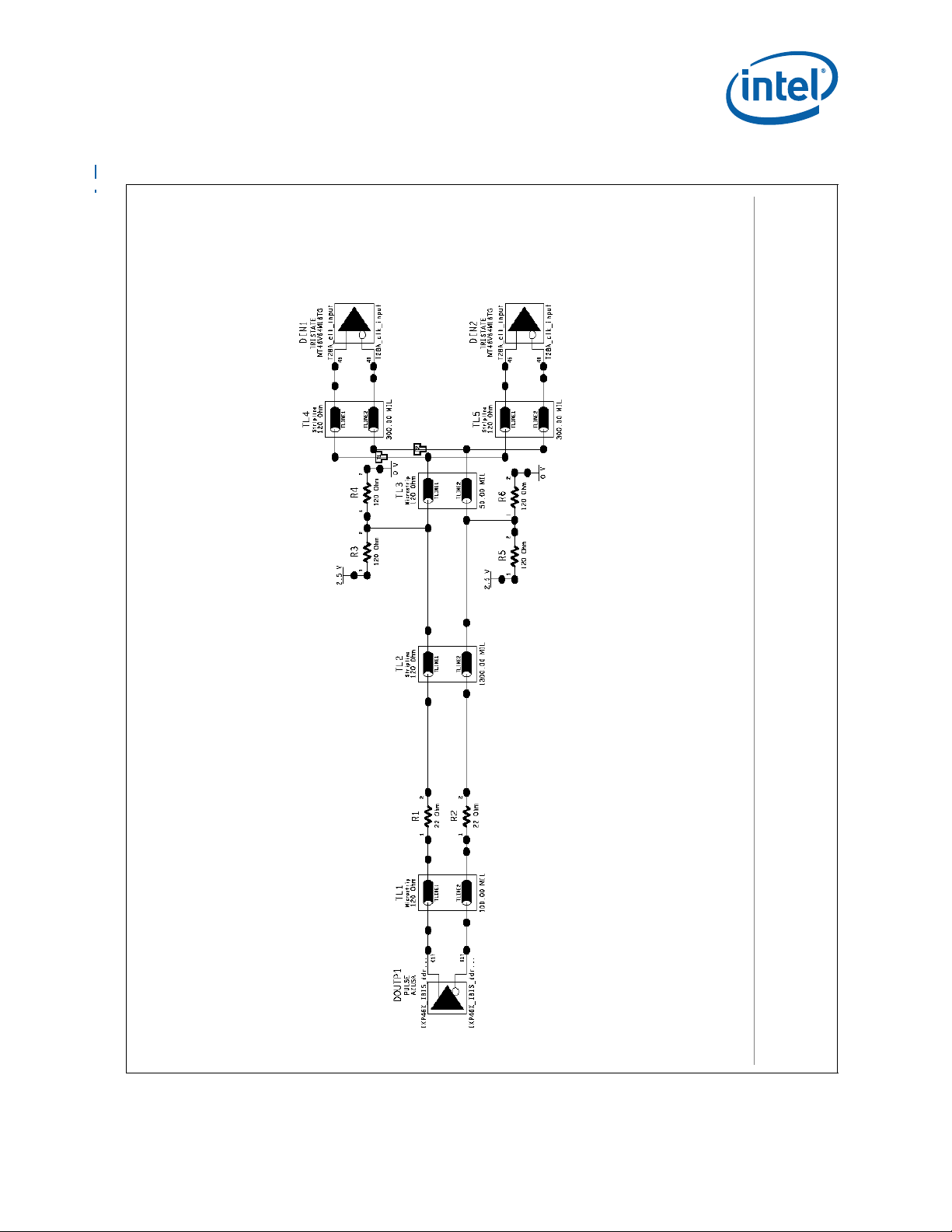
DDR-SDRAM—Intel
®
IXP45X and Intel® IXP46X Product Line of Network Processors
Figure 37. DDR Clock Topology: Two-Bank x16 Devices
February 2007 HDD
Document Number: 305261, Revision: 004 91
Intel® IXP45X and Intel® IXP46X Product Line of Network Processors
Page 92

Intel® IXP45X and Intel® IXP46X Product Line of Network Processors—Category
Figure 38. DDR Clock Simulation Results: Two-Bank x16 Devices
The differential-clock-circuit simulation in Figure 38 shows that the voltage waveform
meets the DDR device input voltage requirements. The crossing point for the clock
input must occur between V
peak to peak swing of 700 mV. The receiver input waveform must also not exceed a
maximum voltage of V
in(max)
=1.05 V and V
ix(min)
ix(max)
=1.45 V and have a minimum
=2.8 V or the minimum voltage of V
in(min)
=-0.3 V.
Waveform results for device DDR_DEVICE2 is not shown as it is identical to that of
device DDR_DEVICE1 due to symmetry. When final routing data is available, simulation
results for all receivers are analyzed as variations in routing may result in differences.
These differences should be minimal.
7.2.2 Data Group
The data signal group includes the signals DDRI_CB[7:0], DDRI_DQ[31:0],
DDRI_DQS[4:0], and DDRI_DM[4:0]. The following simulations were constructed for
the 2 bank x16 device configuration where each signal would have two receivers where
only one is active for a read or write.
Table 37 identifies the transmission line lengths for the data (DDRI_DQ5) topology
shown in Figure 39 on page 94. These lengths were chosen as realistic goals given the
IXP45X/IXP46X network processors to DDR device body to body separation of no more
than 500 mils.
®
IXP45X and Intel® IXP46X Product Line of Network Processors
Intel
HDD February 2007
92 Document Number: 305261, Revision: 004
Page 93
DDR-SDRAM—Intel
®
IXP45X and Intel® IXP46X Product Line of Network Processors
Table 37. Data Group Topology Transmission Line Characteristics
Transmission Line Length
TL1 (T
= 175 ps/in) ~600 mils
pd
TL2 (T
= 175 ps/in) ~50 mils
pd
TL3 (T
= 175 ps/in) ~1,100 mils
pd
TL4 (T
= 175 ps/in) ~50 mils
pd
TL5, TL6 (T
TL7, TL8 (T
= 175 ps/in) ~300 mils
pd
= 175 ps/in) ~800 mils
pd
February 2007 HDD
Document Number: 305261, Revision: 004 93
Intel® IXP45X and Intel® IXP46X Product Line of Network Processors
Page 94

Intel® IXP45X and Intel® IXP46X Product Line of Network Processors—Category
Figure 39. DDR Data Topology: Two-Bank x16 Devices
®
IXP45X and Intel® IXP46X Product Line of Network Processors
Intel
HDD February 2007
94 Document Number: 305261, Revision: 004
Page 95

DDR-SDRAM—Intel
®
IXP45X and Intel® IXP46X Product Line of Network Processors
Figure 40. DDR Data Write Simulation Results: Two-Bank x16 Devices
The data-circuit simulation results in Figure 40 show that the voltage waveform meets
the DDR device input voltage requirements. V
V
The receiver waveform must also not exceed a maximum voltage of V
the minimum voltage of V
ih(min)
of V
+ 0.310 or 1.56 V are easily achieved at the receiver (DDR_DEVICE1).
ref
=-0.3 V.
in(min)
il(max)
of V
– 0.310 or 940 mV and
ref
in(max)
= 2.8 V or
Waveform results for DDR_DEVICE2 are not shown as it is identical to that of device
DDR_DEVICE1 due to symmetry . When final routing data is available, simulation results
for all receivers are analyzed as variations in routing may result in differences. These
differences should be minimal.
February 2007 HDD
Document Number: 305261, Revision: 004 95
Intel® IXP45X and Intel® IXP46X Product Line of Network Processors
Page 96

Intel® IXP45X and Intel® IXP46X Product Line of Network Processors—Category
Figure 41. DDR Data Read Simulation Results: Two-Bank x16 Devices
(Reduced Drive Strength)
The simulation results in Figure 41 are for the data circuit with a DDR device using
reduced drive strength and shows that the voltage waveform meets the DDR device
input voltage requirements. V
0.150 or 1.40 V are easily achieved at the receiver (IXP45X/IXP46X network
il(max)
of V
– 0.150 or 1.10 V and V
ref
ih(min)
of V
ref
+
processors). The receiver waveform must also not exceed a maximum voltage of
V
in(max)
=2.8 V or the minimum voltage of V
in(min)
=-0.3 V.
Waveform results for DDR_DEVICE2 are not shown as it is not relevant when reading
from DDR_DEVICE1. Due to the symmetry of the topology, waveform results when
reading from DDR_DEVICE2 would be identical to those when reading from
DDR_DEVICE1. When final routing data is available, simulation results for all receivers
are analyzed as variations in routing may result in differences. These differences should
be minimal.
®
IXP45X and Intel® IXP46X Product Line of Network Processors
Intel
HDD February 2007
96 Document Number: 305261, Revision: 004
Page 97

DDR-SDRAM—Intel
®
IXP45X and Intel® IXP46X Product Line of Network Processors
Figure 42. DDR Data Read Simulation Results: Two-Bank x16 Devices (Full Drive
Strength)
The simulation results in Figure 42 are for the data circuit with a DDR device using full
drive strength and show that the voltage wa veform meets the DDR device input voltage
requirements. V
are easily achieved at the receiver (IXP45X/IXP46X network processors). However, the
il(max)
of V
receiver waveform must also not exceed a maximum voltage of V
minimum voltage of V
network processors are close to these limits. A larger series resistor could be used to
in(min)
– 0.150 or 1.10 V and V
ref
= -0.3 V and the waveforms at the IXP45X/IXP46X
ih(min)
of V
+ 0.150 or 1.40 V
ref
in(max)
= 2.8 V or the
attenuate the signal, but the results of doing so might have an adverse effect on write
operations.
Waveform results for DDR_DEVICE2 are not shown as it is not relevant when reading
from DDR_DEVICE1. Due to the symmetry of the topology, waveform results when
reading from DDR_DEVICE2 would be identical to those when reading from
DDR_DEVICE1. When final routing data is available, simulation results for all receivers
are analyzed as variations in routing may result in differences. These differences should
be minimal.
February 2007 HDD
Document Number: 305261, Revision: 004 97
Intel® IXP45X and Intel® IXP46X Product Line of Network Processors
Page 98

Intel® IXP45X and Intel® IXP46X Product Line of Network Processors—Category
7.2.3 Control Group
The control signal group includes the signals DDRI_CS[1:0] and DDRI_CKE[1:0]. The
following simulations were constructed for the 2 bank x16 device configuration where
each signal would have three receivers.
Table 38 identifies the transmission line lengths for the chip select (CS0) topology
shown in Figure 43 on page 98. These lengths were chosen as realistic goals given the
IXP45X/IXP46X network processors to DDR body to body separation of no more than
500 mils.
Table 38. Control Group Topology Transmission Line Characteristics
Transmission Line Le ngth
TL1 (T
= 175 ps/in) ~ 600 mils
pd
TL2 (T
= 175 ps/in) ~ 50 mils
pd
TL3 (T
= 175 ps/in) ~ 1,100 mils
pd
TL4 (T
= 175 ps/in) ~ 50 mils
pd
TL5, TL6, TL7 (T
TL8, TL9, TL10 (T
= 175 ps/in) ~ 800 mils
pd
= 175 ps/in) ~ 300 mils
pd
Figure 43. DDR Control (CS0) Topology: Two-Bank x16 Devices
®
IXP45X and Intel® IXP46X Product Line of Network Processors
Intel
HDD February 2007
98 Document Number: 305261, Revision: 004
Page 99

DDR-SDRAM—Intel
®
IXP45X and Intel® IXP46X Product Line of Network Processors
Figure 44. DDR RAS Simulation Results: Two-Bank x16 Devices
The simulation results in Figure 44 are for the control circuit and show that the voltage
waveform meets the DDR device input voltage requirements. V
940 mV and V
(DDR_DEVICE1). The receiver waveform must also not exceed a maximum voltage of
V
in(max)
= 2.8 V or the minimum voltage of V
ih(min)
of V
+ 0.310 or 1.56 V are easily achieved at the receiver
ref
= -0.3 V.
in(min)
il(max)
of V
– 0.310 or
ref
Waveform results for DDR_DEVICE2 and DDR_DE VICE3 are not shown as it is identical
to that of DDR_DEVICE1 due to symmetry. When final routing data is available,
simulation results for all receivers are analyzed as variations in routing may result in
differences. These differences should be minimal.
February 2007 HDD
Document Number: 305261, Revision: 004 99
Intel® IXP45X and Intel® IXP46X Product Line of Network Processors
Page 100

Intel® IXP45X and Intel® IXP46X Product Line of Network Processors—Category
7.2.4 Command Group
The command signal group includes the signals DDRI_MA[13:0], DDRI_BA[1:0],
DDRI_RAS, DDRI_CAS and DDRI_WE. The following simulations were constructed for
the 2 bank x16 device configuration where each signal would have six receivers.
Table 39 identifies the transmission line lengths for the address (DDRI_MA3) topology
shown in Figure 45 and Figure 47. These lengths were chosen as realistic goals given
the IXP45X/IXP46X network processors to DDR body to body separation of no more
than 500 mils.
Table 39. Command Group Topology Transmission Line Characteristics
Transmission Line Length
TL1 (T
= 175 ps/in) ~ 600 mils
pd
TL2 (T
= 175 ps/in) ~ 50 mils
pd
TL3 (T
= 175 ps/in) ~ 1,100 mils
pd
TL4 (T
= 175 ps/in) ~ 50 mils
pd
TL5, TL8, TL11 (T
TL6, TL7, TL9, TL10, TL12, TL13 (T
= 175 ps/in) ~ 800 mils
pd
= 175 ps/in) ~ 300 mils
pd
®
IXP45X and Intel® IXP46X Product Line of Network Processors
Intel
HDD February 2007
100 Document Number: 305261, Revision: 004
 Loading...