

Page 1
iSBC 80/30
SINGLE BOARD
COMPUTER
HARDWARE
REFERENCE MANUAL
Manual Order Number: 9800611 A
I
Corporation. 3065 Bowers Avenue, Santa Clara, California 95051
Intel
Copyrightf
l
1978 Intel Corporation
I
Page 2
The
information
Intel
Corporation
to,
the
implied
assumes
no
commitment
No
part
written
The
of
consent
following
in
this
makes
warranties
responsibility
to
update
this
document
of
-Intel
are
trademarks
document
no
warranty
of
merchantability
for
any
nor
to
keep
may
be
Corporation.
of
Intel
is
subject
of
errors
current
copied
Corporation
to
any
kind
that
may
the
or
reproduced
change
without
with
regard
and
fitness
appear
information
and
may
notice.
to
this
for a particular
in
this
document.
contained
in
any
form
be
used
only
material,
in
this
document.
or
by
any
to
describe
including,
purpose.
Intel
Corporation
means
Intel
Intel
but
Corporation
without
products:
not
makes
the
limited
no
prior
ICE
INSITE
INTEL
INTELLEC
iSBC
ii
LIBRARY
MANAGER
MCS
MEGACHASSIS
MICROMAP
MULTI
BUS
Printed in
PROMPT
RMX
UPI
"SCOPE
U.S.A./852/067817.5K
TL
Page 3
PREFACE
This manual provides general information, installation, programming information,
of
principles
Computer. Additional information
• Intel MCS-85 User's Manual, Order No. 98-366
• Intel UPI-41 User's Manual, Order No. 9800504
• Intel 8080/8085 Assembly Language Programming Manual, Order No. 9800301
• Intel 8255A Programmable Peripheral Interface, Application Note AP-15
• Intel 8251 Universal Synchronous/Asynchronous Receiver/Transmitter, Application
Note AP-16
• Intel MULTIBUS Interfacing, Application Note AP-28
• Intel 8259 Programmable Interrupt Controller, Application Note AP-31
operation, and service information for the Intel iSBC 80/30 Single Board
is
available
in
the following documents:
iii
Page 4
CHAPTER 1
GENERAL INFORMATION
Introduction
Description
System Software Development
Equipment Supplied . . . . . . . . . . . . ... . . . . . . . . . . . . . .
Equipment Required . . . . . . . . . . . . . . . . . . . . . . . . . . . .
Specifications
..............
.....................................
...................................
: . . . . . . . . . . . . . . . . . . . .
..............
'
.......
CHAPTER 2
FOR
PREPARATION
Introduction. . . . . . . . . . . . . . . . . . . . . . . . . . . . . . . . . . .
Unpacking and Inspection
Installation Considerations . . . . . . . . . . . . . . . . . . . . . . .
User-Furnished Components
Power Requirements. . . . . . . . . . . . . . . . . . . . . . . . . .
Cooling Requirement
Physical Dimensions
Component Installation
ROM/EPROM Chips
Universal Peripheral Interface
Line Drivers and
Rise Time/Noise Capacitors
Jumper Configuration. . . . . . . . . . . . . . . . . . . . . . . . . . .
ROM/EPROM Configuration
On-Board RAM Addresses
On-Board 8085A Access
System Access
Priority Interrupts
8251A
Port Configuration
Port Configuration
8255A
8041/8741A
Multibus Configuration
Signal Characteristics
Serial Priority Resolution
Parallel Priority Resolution
Power Fail/Memory Protect Configuration
Parallel
Serial
Board Installation
I/O Cabling
I/O Cabling
I/O Terminators . . . . . . . . . . . . . . .
..............................
..............................
Port Configuration
..............................
................................
................................
USE
.........................
.....................
..
. . . . . . . . . . . . . . . . . . . . . . .
............................
............................
...........................
....................
......................
.....................
......................
......................
.......................
.......................
...................
...........................
...........................
........................
......................
............
CHAPTER 3
PROGRAMMING INFORMATION
Introduction. . . . . . . . . . . . . . . . . . . . . . . . . . . . . . . . . . .
Timer.
Failsafe
Memory Addressing
I/O Addressing
System Initialization
8251A USART Programming
Mode Instruction Format
Sync Characters
Command Instruction Format
Reset
Addressing
Initialization
. . . . . . . . . . . . . . . . . . . . . . . . . . . . . . . .
..............................
..................................
..............................
......................
........................
...............................
....................
........................................
...................................
..................................
PAGE
..
1-1
1-1
1-3
..
1-4
..
1-4
1-4
..
2-1
2-1
..
2-1
2-1
..
2-1
..
2-1
2-1
2-3
2-3
2-4
..
2-4
2-4
..
2-4
2-4
2-4
2-7
2-7
2-8
2-12
2-12
2-12
2-15
2-15
2-23
2-24
2-24
2-27
2-27
2-29
..
3-1
..
3-1
3-1
3-2
3-2
3-3
3-3
3-3
3-3
3-4
3-4
3-4
CONTENTS
Operation
8253
Mode Control Word and Count
Addressing
Initialization
Operation
8255A
Control Word Format
Addressing
Initialization
Operation
8259A
Interrupt Priority Modes
Interrupt Mask
Status Read
Initialization Command Words
Operation Command Words
Addressing
Initialization
Operation
8041/8741A UPI Programming
Interrupt Handling
TRAP Input
RST 7.5, 6.5, 5.5 Inputs
INTR Input
CHAPTER 4
PRINCIPLES
Introduction. . . . . . . . . . . . . . . . . . . . . . . . . . . . . . . . . . .
Functional Description . . . . . . . . . . . . . . . . . . . . . . . . . .
Clock Circuits . . . . . . . . . . . . . . . . . . . . . . . . . . . . . . .
Central Processor Unit . . . . . . . . . . . . . . . . . . . . . . . .
Interval
Serial
Parallel
Universal Peripheral Interface
Interrupt Control. . . . . . . . . . . . . . . . . . . . . . . . . . . . .
ROM/EPROM Configuration. . . . . . . . . . . . . . . . . . .
RAM Configuration
Bus Interface
Dual-Port Control
Circuit Analysis
.....................................
Data
Input/Output
Status Read . . . . . . . . . . . . . . . . . . . . . . . . . . . . . . .
PIT Programming
...................................
.....................................
Counter Read
Clock Frequency/Divide Ratio Selection
Rate Generator/Interval Timer
Interrupt Timer
PPI Programming
...................................
.....................................
Read
Operation
Operation
Write
PIC Programming
Fully Nested Mode
Auto-Rotating Mode
Specific Rotating Mode
...................................
.....................................
Timer.
I/O . . . . . . . . . . . . . . . . . . . . . . . . . . . . . . . . . . .
I/O . . . . . . . . . . . . . . . . . . . . . . . . . . . . . . . . .
............................
...........................
...................
..................................
...............................
..................
..............................
..........................
...........................
..................................
..............................
.............................
..........................
.........................
...........................
..........................
.......................
................................
...................
......................
...................................
..................................
.....................
...............................
...................................
........................
...................................
OF
OPERATION
. . . . . . . . . . . . . . . . . . . . .
..
. . . . . . . . . . . . . . . .
............................
..................................
..............................
...................
'
..........
..
. . . . . . .
............. ; ....
PAGE
3-5
3-5
..
3-6
3-6
3-7
3-10
3-10
3-11
3-11
3-11
3-12
3-12
3-13
3-13
3-14
3 -14
3-14
3-14
3-14
3-14
3-14
3-14
3-15
3-15
3-15
3-15
3-15
3-16
3-16
3 -16
3-16
3-17
3-22
3-22
3-23
3 -
..
4-1
..
4-1
..
4-1
..
4-1
..
4-1
..
4-1
..
4-1
..
4-2
..
4-2
..
4-2
4-2
4-2
4-2
'.
4-2
23
iv
Page 5
CONTENTS (Continued)
Initialization
Clock Circuits
SOS5A
Instruction Timing
Opcode Fetch Timing. . . . . . . . . . . . . . . . . . . . . . .
Memory Read Timing
I/O Read Timing
Memory Write Timing
I/O Write Timing
Interrupt Acknowledge Timing
Address Bus
Bus Time
Data Bus
Read/Write
I/O Control Signals. . . . . . . . . . . . . . . . . . . . . . . . .
Memory Control
_ Dual Port Control Logic. . . . . . . . . . . . . . . . . . . . . . .
Bus Access Timing
CPU Access Timing
Multibus Interface
I/O Operation
........ -..........................
.................................
CPU Timing
Out
.....................................
Signal Generation . . . . . . . . . . . . . . . . . .
....
'"
.....................
...........................
........................
.............................
........................
............................
.................
..................................
.................................
Signals
.............................
................................
......................
..........................
.........................
PAGE
4-2
4-3
4-3
4-3
..
4-4
4-6
4-6
4-6
4-7
4-7
4-9
4-9
'4-9
..
4-9
..
4-9
4-9
..
4-9
.4-12
.4-12
.4-12
.4-13
On-Board I/O Operation
System I/O Operation
ROM/EPROM Operation
RAM
Operation
RAM Controller
On-Board Read/Write Operation
Bus Read/Write
Interrupt
Operation
..............................
............................
Operation
............................
.....................
........................
........ ' ...............
...............
....................
CHAPTER 5
SERVICE
Introduction . . . . . . . . . . . . . . . . . . . . . . . . . . . . . . . . . . .
Replaceable
Service Diagrams
Service and Repair Assistance
INFORMATION
Parts
............................
................................
......................
;
APPENDIX A
8085
INSTRUCTION SET
APPENDIX B
TELETYPEWRITER
MODIFICATIONS
PAGE
.4-13
.4-13
.4-13
.4-14
.4-14
.4-14
.4-14
.4-15
..
5-1
...
5-1
5-1
5-1
TABLE
1-1.
2-1.
2-2.
2-3.
2-4.
2-5.
2-6.
2-7.
2-8.
2-9.
2-10.
2-11.
2-12.
2-13.
2-14.
TITLE
Specifications
User-Furnished and Installed Components
User-Furnished Connector Details
Line Driver and I/O Terminator Locations
Jumper
ROM/EPROM Configuration Jumpers
Jumper Configuration for
8085A CPU
65K
Page System Memory Selection
SK/16K
Priority
Connector
Jumper Configuration
8255A
Multibus Connector
Multibus Signal Functions
iSBC 80/30 DC Characteristics
...........................
...........
Selectable Options. . . . . . . . . . . . . . .
.......
Access
Block Selection Within 65K Page
Interrupt Jumper Matrix
13
Pin Assignments Vs.
Port Configuration Jumpers
On-Board
of
On-Board RAM
...................
PI
Pin Assignments
.................
........
............
..........
.............
....
....
....
....
.....
PAGE
1-4
2-2
2-3
2-4
..
2-5
2-7
2-7
2-S
2-S
2-11
2-12
2-13
2-16
2-17
2-18
TABLE
2-15.
2-16.
2-17.
2-18.
2-19.
2-20.
2-21.
2-22.
3-1.
3-2.
3-3.
3-4.
TABLES
TITLE PAGE
lSBC 80/30
(Master Mode)
iSBC
AuxHiary Connector P2 Pin Assignments
Auxiliary
DC Characteristics
Connector
Connector 12 Pin Assignments
Parallel I/O Signal (Connector 11/12)
DC Characteristics
Connector
On-Board
I/O Address Assignments
Typical USART Mode or Command
Instruction
Typical USART Data Character
Read Subroutine
'At
Characteristics
SO/3~
Signal (Connector P2)
........................
AC Characteristics (Slave Mode) .2-21
11
Pin Assignments
13
Vs. RS232C Pin COITl!spondence2-29
Memory Address (for CPU Access) 3-1
Subroutine
.....................
.............
.............
.....................
.........•........
..................
.......................
.....
2-21
2-26
2-26
2-27
2-27
2-2S
3-2
3-5
3-6
v
Page 6
TABLES (Continued)
TABLE
3-5.
3-6.
3-7.
3-8.
3-9.
3-10.
3-11.
3-12.
3-13.
3-14.
3-15.
3-16.
3-17.
TITLE
Typical USART Data Character
Write Subroutine
Typical
PIT Counter Operation Vs. Gate Inputs
Typical
Typical
Typical
PIT Count Value Vs. Rate Multiplier
PIT Rate Generator Frequencies and
PIT Time Intervals Vs. Timer Counts
Typical
Typical
Typical
PIC Device Address Insertion
USART Status Read Subroutine
PIT Control Word Subroutine
PIT Count Value Load Subroutine
PIT Counter Read Subroutine
for Each Baud Rate
Timer Intervals
PPI Initialization Subroutine
PPI Port Read Subroutine
PPI Port Write Subroutine
.......................
...................
....
c
••••••••••••••••••••
..............
.........
...........
..........
.....
......
.......
.......
.......
PAGE
3-6
3-7
3-10
3-10
...
3-11
3-11
.3-12
3-13
3-13
3-14
3-14
3 -15
3-16
TABLE
3~18.
3-19.
3-20.
3-21.
3-22.
3-23.
3-24.
3-25.
3-26.
3-27.
4-1.
5-1.
5-2.
TITLE
Typical PIC Initialization Subroutine
PIC Operation Procedures
Typical
Typical PIC In-Service Register
Typical PIC Set Mask Register Subroutine
Typical PIC Mask Register Read Subroutine
Typical
Typical UPI Data Byte Read Subroutine
Typical
CPU Status and Control Lines. . . . . . . . . . . .
Replaceable
PIC Interrupt Request Register
Read Subroutine
Read Subroutine
PIC End-of-Interrupt
Command Subroutine
UPI Data Byte Write Subroutine
8085A CPU Restart Interrupt
Parts
List of Manufacturers' Codes
..........
.................
.......................
..... ' .. ' ................
...................
........
.....
.....
V~ctors
........
,.............
..............
....
ILLUSTRATIONS
PAGE
3'-17
3-19
3-20
3-20
3-20
..
3-21
3-21
3-22
3-22
3-22
..
4-4
5-1
5-3
FIGURE
1-1.
2-1.
2-2.
2-3.
2-4.
2-5.
2-6.
3-1.
3-2.
3-3.
3-4.
3-5.
3-6.
. 3-7.
3-8.
3-9.
3-10.
3-11.
TITLE
iSBC 80/30 Single Board Computer . . . . . . .
Jumper Configuration for Multibus Access
On-Board RAM (16-Bit Address System)
Jumper Configuration for Multibus Access
On-Board RAM (20-Bit Address System)
Bus Exchange Timing (Master Mode)
Bus Exchange Timing (Slave Mode)
Priority Resolution Scheme
Serial
Parallel Priority Resolution Scheme
USART Synchronous Mode Instruction
Word Format
USART Synchronous Mode Transmission
Format
USART Asynchronous Mode Instruction
Word Format
USART Asynchronous Mode Transmission
Format
USART Command Instruction Word Format
Typical
USART Status Read Format
PIT Mode Control Word Format
PIT Programming Sequence Examples
PIT Counter Register Latch Control
PPI Control Word Format
USART Initialization and
I/O Data Sequence
Word Format.
..........................
...............................
..........................
...............................
.....................
...............
.........................
.................
.......
.........
...........
.........
............
.......
PAGE
..
of
..
of
..
..
1-1
2-9
2-10
2-22
2-23
2-24
2-25
3-3
3-3
3-3
3-4
3-4
3-5
3-7
3-8
3-9
3-.12
3-13
FIGURE
3-12.
3-13.
3-14.
3-15.
3-16.
4.-1.
4-2.
4-3.
4-4.
4-5.
4-6.
4-7.
4-8.
4-9.
4-10.
5-1.
5-2.
5-3.
5-4.
TITLE
PPI Port C Bit Set/Reset Control
Word Format
PIC Device Interrupt Addresses
PIC Initialization Command Word Formats
PIC Operation Control Word Formats
UPI Data Bus Buffer and
Status Registers
80/30 Input/Output and
iSBC
Interrupt Block Diagram
iSBC
80/30 ROM/EPROM and Dual Port
RAM Block Diagram
Typical
Opcode Fetch Machine Cycle
Opcode Fetch Machine Cycle (With Wait)
Memory Read (or
Memory Write (or
Interrupt Acknowledge Machine Cycles
Dual
Port Control Bus Access Timing
With
Port Control CPU Access Timing
Dual
With Bus Lockout
iSBC
80/30 Parts Locations Diagram
iSBC
80/30 Schematic Diagram
iSBC
604 Schematic Diagram
iSBC 614 Schematic Diagram
..........................
........................
...............
CPU Instruction Cycle
CPU Lockout
..................
I/O Read) Machine Cycles . 4-6
I/O Write) Machine Cycles 4-7
....................
....................
.............
........
.............
..............
......
........
............
..............
..............
PAGE
...
....
3-15
3-16
3 -17
3-18
3-21
.4-17
.4-19
4-4
4-5
4-5
4-8
.4-10
.4-11
5-5
5-7
5-25
5-27
vi
Page 7
CHAPTER 1
1-1. INTRODUCTION
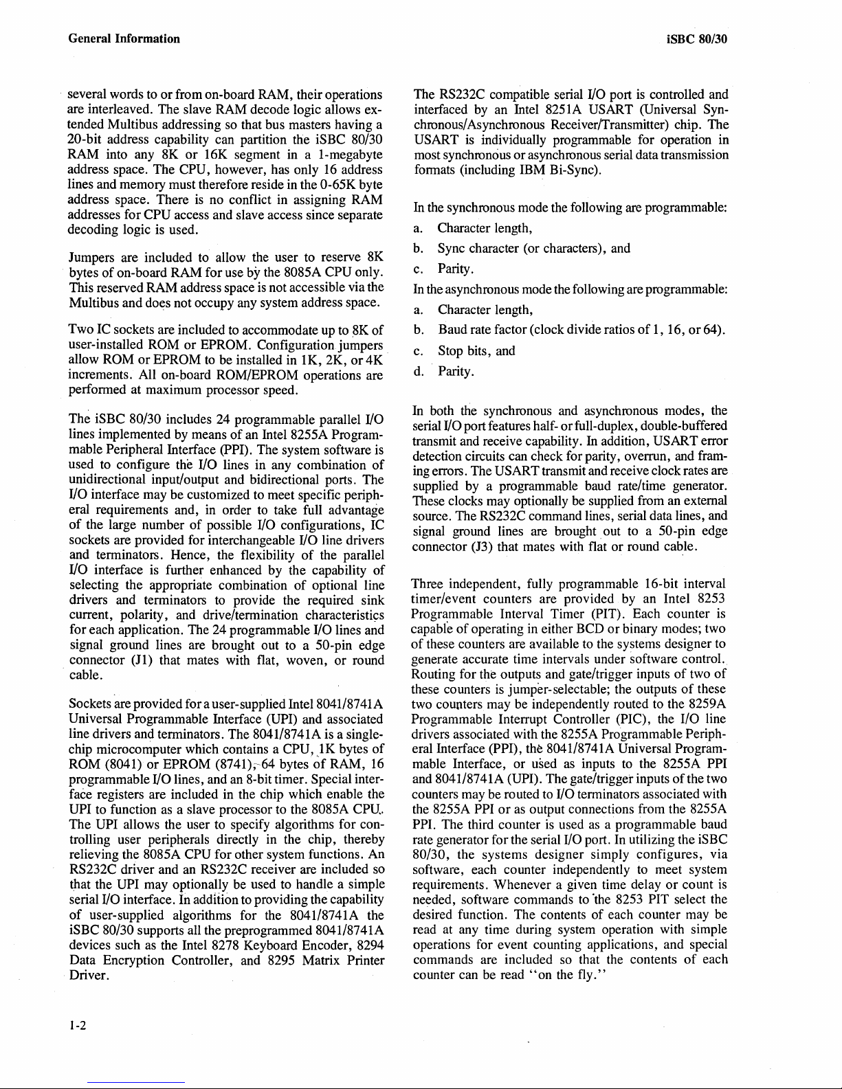
The iSBC 80/30 Single Board Computer, which
member
products,
circuit assembly. The iSBC
cessor unit
of
Intel's complete line
is
a computer system on a single printed-
of
iSBC 80 computer
80/30 includes a central pro-
(CPU),
16K
bytes
of
dynamic random access
memory (RAM), one serial and three parallel I/O ports,
a programmable
bus control logic. Also included
to allow the iSBC
to
other bus masters
for user-installation
only memory
timer~
80/30 to act
in
of
(ROM
or
priority interrupt logic, and Multi-
is
dual port control logic
as
a slave RAM device
the system. Provision is made
masked or programmable read
EPROM) and an Intel 8041
8741A Universal Peripheral Interface.
is
or
1-2. DESCRIPTION
The iSBC 80/30 Single Board Computer (figure 1-1)
controlled by an Intel 8085A Microprocessor (CPU),
which includes six 8-bit general-purpose registers and an
accumulator. The six general-purpose registers may be
addressed individually
or
in pairs, which allows both
single precision and double precision operations. The
CPU has a 16-bit program counter which allows direct
is
GENERAL
addressing
located within any portion
used
as
a
a last-in/first-out storage area for the contents
of
up
INFORMATION
to
65K
of
memory. An external stack,
of
read/write memory, may be
the program counter, flags, accumulator, and all six
general-purpose registers. A 16-bit stack pointer controls
the addressing
routine nesting that
of
this external stack, which allows sub-
is
bounded only by the 65K address
limitation.
The iSBC
80/30 has an internal bus for all on-board
memory and I/O operations and accesses the system bus
(Multibus) for all external memory and
Hence, local (on-board) operations do not involve the
Multibus and allow true parallel processing when several
bus masters (e.g., DMA devices and other single board
computers) are used in a multimaster scheme.
The
16K
of
dynamic RAM
2717 chips and an Intel
is
implemented with eight Intel
8202 Dynamic RAM Controller.
Dual port control logic is included to interface this 16K
RAM with the Multibus
so
that the iSBC 80/30 can function as a slave RAM device when not in control
Multibus. The
RAM. After the
tion, the controlling bus master
CPU has priority when accessing on-board
CPU completes its read
is
allowed
and complete its operation. Where both the
controlling bus master have the need to write
of
I/O operations.
of
the
or
write opera-
to
access RAM
CPU and the
or
read
611-1
PARALLEL
1/0
(MULTIBUS) (AUXILIARY)
OPTIONAL
8041/8741
1/0
SERIAL
1/0
Figure 1-1. iSBC 80/30 Single Board Computer
1-1
Page 8
General Information
iSBC
80/30
several words to
or
from on-board RAM, their operations
are interleaved. The slave RAM decode logic allows ex-
so
tended Multibus addressing
that bus masters having a
20-bit address capability can partition the iSBC 80/30
RAM into any 8K
address space. The
lines and memory must therefore reside in the
address space. There
addresses for
or
16K segment in a I-megabyte
CPU, however, has only
16
address
0-65K byte
is
no conflict in assigning RAM
CPU access and slave access since separate
decoding logic is used.
Jumpers are included to allow the user to reserve 8K
bytes
of
on-board RAM for use by the 8085A CPU only.
This reserved RAM address space
is
not accessible via the
Multibus and does not occupy any system address space.
Two IC sockets are included to accommodate up
user-installed ROM
allow
ROM
or
increments. All on-board
or
EPROM
EPROM. Configuration jumpers
to
be installed in
ROM/EPROM operations are
lK,
2K,
to
.8K
or
of
4K
performed at maximum processor speed.
iSBC 80/30 includes 24 programmable parallel I/O
The
lines implemented by means
of
an Intel 8255A Programmable Peripheral Interface (PPI). The system software is
used to configure
the I/O lines in any combination
of
unidirectional input/output and bidirectional ports. The
I/O interface may be customized to meet specific peripheral requirements and, in order
of
the large number
of
possible I/O configurations, IC
sockets are provided for interchangeable
and terminators. Hence, the flexibility
I/O interface
is
further enhanced by the capability
selecting the appropriate combination
drivers and terminators
to
current, polarity, and drive/termination
to
take full advantage
I/O line drivers
of
the parallel
of
of
optional line
provide the required sink
characteristi9s
for each application. The 24 programmable I/O lines and
signal ground lines are brought out to a
connector
(11)
that mates with flat, woven, or round
50-pin edge
cable.
Sockets are provided
Universal Programmable Interface
fora
user-supplied Inte18041/8741A
(UPI) and associated
line drivers and terminators. The 8041/8741A is a singlechip microcomputer which contains a
ROM (8041)
or
EPROM
(8741),64
CPU, ) K bytes
bytes
of
RAM,
of
16
programmable I/O lines, and an 8-bit timer. Special interface registers are included in the chip which enable the
UPI to function as a slave processor to the 8085A CPU.
The UPI allows the user to specify algorithms for con-
trolling user peripherals directly in the chip, thereby
relieving the
RS232C driver and an RS232C receiver are included
8085A CPU for other system functions. An
so
that the UPI may optionally be used to handle a simple
serial
I/O interface. In addiiion to providing the capability
of
user-supplied algorithms for the 8041/8741A the
iSBC 80/30 supports all the preprogrammed 8041/8741A
devices such
Data Encryption Controller, and 8295 Matrix
as
the Intel 8278 Keyboard Encoder, 8294
Printer
Driver.
The RS232C compatible serial I/O port
interfaced
by
an Intel 8251A
US
is
controlled and
ART (Universal Synchronous/Asynchronous Receiver/Transmitter) chip. The
USART
most synchronous
is
individually programmable for operation in
or
asynchronous serial data transmission
formats (including IBM Bi-Sync).
In
the synchronous mode the following are programmable:
a.
Character length,
b.
Sync character (or characters), and
c.
Parity.
In the asynchronous mode the following are programmable:
a.
Character length,
b.
Baud rate factor (clock divide ratios
Stop bits, and
c.
d
..
Parity.
of
1, 16,
or
64).
In both the synchronous and asynchronous modes, the
I/O port features half-
serial
transmit and receive capability. In addition,
or
full-duplex, double-buffered
USART error
detection circuits can check for parity, overrun, and framing errors. The
USART transmit and receive clock rates are
supplied by a programmable baud rate/time generator.
These clocks may optionally be supplied from an external
source. The RS232C command lines, serial data lines, and
signal ground lines are brought. out to a
(13)
connector
that mates with flat
or
50-pin edge
round cable.
Three independent, fully programmable 16-bit interval
timer/event counters are provided by an Intel 8253
Programmable Interval Timer (PIT). Each counter
capable
of
of
operating in either BCD
or
binary modes; two
these counters are available to the systems designer to
is
generate accurate time intervals under software control.
Routing for the outputs and gate/trigger inputs
these counters
is
jumper-selectable; the outputs
of
of
two
these
of
two counters may be independently routed to the 8259A
Programmable Interrupt Controller (PIC), the
drivers associated with the 8255A Programmable
I/O line
Periph-
eral Interface (PPI), the 8041/8741A Universal Program-
mable Interface, or used
and 8041/8741A (UPI). The gate/trigger inputs
counters may be routed
the 8255A
PPI
or
as
PPI. The third counter
rate generator for the serial
80/30,
the systems designer simply configures, via
software, each counter independently
requirements. Whenever a given time delay
needed, software commands
desired function. The contents
as
inputs to the 8255A PPI
ofthe
two
to
I/O terminators associated with
output connections from the 8255A
is
used
as
a programmable baud
I/O port. In utilizing the iSBC
to
meet system
or
count
is
to
·the 8253 PIT select the
of
each counter may be
read at any time during system operation with simple
operations for event counting applications, and special
so
commands are included
counter can be read
"on
that the contents
the
fly."
of
each
1-2
Page 9

iSBC 80/30
The iSBC 80/30 provides vectoring for
of
levels, four
processing capability
(TRAP, RST
levels
(in decreasing order
interrupts
ate the following unique
RST
7.5
8085A JUMP instruction at each
provides linkage
which are handled directly by the interrupt
of
the 8085A CPU. These four
7.5;
RST
6.5,
and RST 5.5) represent
of
priority) the four highest priority
of
the iSBC 80/30. These four interrupts gener-
memory address: TRAP (24H),
(3CH), RST 6.5 (34H), and RST 5.5 (2CH). An
of
these addresses then
to
interrupt service routines located independently anywhere in the lower65K bytes
All interrupt inputs with the exception
masked via software. The
TRAP interrupt should be used
12
interrupt
of
memory.
of
TRAP may be
for conditions such as power-down sequences which require immediate attention by the
An Intel
8259A
Programmable Interrupt Controller
8085A CPU.
(PIC) provides vectoring for the next eight interrupt
levels. The
PIC treats each true input signal condition
as
an interrupt request. After resolving the interrupt priority,
PIC issues a single interrupt request to the CPU.
the
Interrupt priorities are independently programmable
under software control. Similarly, an interrupt can be
masked under software control. The programmable interrupt priority modes are:
a. Fully Nested
fixed priority: input
b. Auto-Rotating
Priority. Each interrupt request has a
0
is
highest, input 7 is lowest.
Priority. Each interrupt request has
equal priority. Each level, after receiving service,
becomes the lowest priority level until the next
interrupt occurs.
c. Specific
Priority
Priority. Software assigns lowest priority.
of
all other levels
is
in numerical sequence
based on lowest priority.
PIC, which can be programmed
The
or
sensitive
level-sensitive inputs, generates a unique
to
respond to edge-
memory address for each interrupt level. These addresses
of
are equally spaced at intervals
or
able) bytes. This 32begin at any 32-
64-byte block may be located to
or
64-byte boundary in the 65,536 byte
4 to 8 (software select-
memory space. A single 8085A JUMP instruction at each
of
these addresses then provides linkage
to
locate each
interrupt service routine independently anywhere in
memory.
General Information
of
request can be generated by two
counters and by the Universal
Peripheral Interface (UPI).
the programmable
Eight additional interrupt request lines are available to the
user for direct interfaces to user designated periphral
devices via the Multibus, and two interrupt request lines
may be jumper routed directly from peripherals via the
parallel
Control logic is also included for generation
I/O driver/ terminator section.
of
a Power-
Fail Interrupt, which works in conjunction with an AC
LOW signal from an Intel iSBC 635 Power Supply
or
equivalent.
iSBC 80/30 includes the resources for supporting a
The
of
OEM
variety
system requirements.
For
those applications requiring additional processing capacity and the
benefits
multiprocessing (i.e., several
CPU's
and/or
of
controllers logically sharing systems tasks with communication over the Multibus), the
iSBC 80/30 provides
full bus arbitration control logic . This control logic allows
of
up to three bus masters (e.g., any combination
80/30, iSBC 80/20,
etc.)
to
share the Multibus in serial (daisy-chain) fashion
or
up
to
16
bus masters to share the Multibus using an
DMA controller, diskette
iSBC
cont~oller,
external parallel priority resolving network.
The Multibus arbitration logic operates synchronously
with the bus clock, which is derived either from the
or
80/30
master. Data, however,
can be optionally generated by some other bus
is
transferred via a handshake
iSBC
between the controlling master and the addressed slave
module. This arrangement allows different speed controllers to share resources on the same bus, and transfers via
the bus proceed asynchronously. Thus, the transfer speed
is
dependent on transmitting and receiving devices only.
This design prevents slower master modules from being
of
handicapped in their attempts to gain control
the bus,
but does not restrict the speed at which faster modules can
transfer data via the same bus. The most obvious appli-
of
cations for the master-slave capabilities
mUltiprocessor configurations, high-speed direct
the bus are
memory
access (DMA) operations, and high-speed peripheral
no
control, but are by
means limited to these three.
Interrupt requests may originate from
jumper-selectable interrupt requests can be automatically
generated by the
(PPI) when a byte
to
the 8085A CPU (i.e., input buffer
Programmable Peripheral Interface
of
information
information has been transferred to a peripheral device
(i.e.,
output buffer
is
empty). Two jumper-selectable
interrupt requests can be automatically generated by the
USART when a character
8085A CPU
character
(i.e.,
receive channel buffer
is
ready to be transmitted (i.e., transmit channel
is
ready to be transferred to the
data buffer is empty). A jumper-selectable interrupt
18
sources. Two
is
ready to be transferred
is
full)
or
a byte
is
full)
or
when a
1-3. SYSTEM SOFTWARE
DEVELOPMENT
Intel's RMX/80 Real-Time Multitasking Software, spe-
of
cifically designed for Intel
puters, provides the capability to monitor and control
mUltiple asynchronous external events. The RMX/80
Executive, which synchronizes and controls the execu-
of
tion
multiple tasks,
relocatable module that requires
memory. Optional linkage and relocatable modules for
iSBC 80 single board com-
is
provided as a linkable and
only
2K
bytes
of
1-3
Page 10
General Information
iSBC 80/30
teletypewriter and CRT control, diskette file system,
high-speed mathematics unit, and analog subsystems are
also available.
The development cycle
of
iSBC 80/30 based products
may be significantly reduced using an Intel Intellec
Microcomputer Development System. The resident
macroassembler, text editor, and system monitor greatly
simplify the design, development, and debug
system software. An optional diskette operating
80/30
system provides
-a
relocating macro assembler, relocating
of
iSBC
loader and linkage editor, and a library manager. A
unique In-Circuit Emulator (lCE-85) option provides the
of
capability
on the
Intel's high level programming language, PL/M,
available
developing and debugging software directly
iSBC 80/30.
as
a resident Intellec Microcomputer Develop-
is
also
ment System option. PL/M provides the capability to pro-
gram
in
a natural, algorithmic language and eliminates the
or
need to manage register usage
allocate memory. PL/M
programs can be written in a much shorter time than
assembly language programs for a given application.
Table
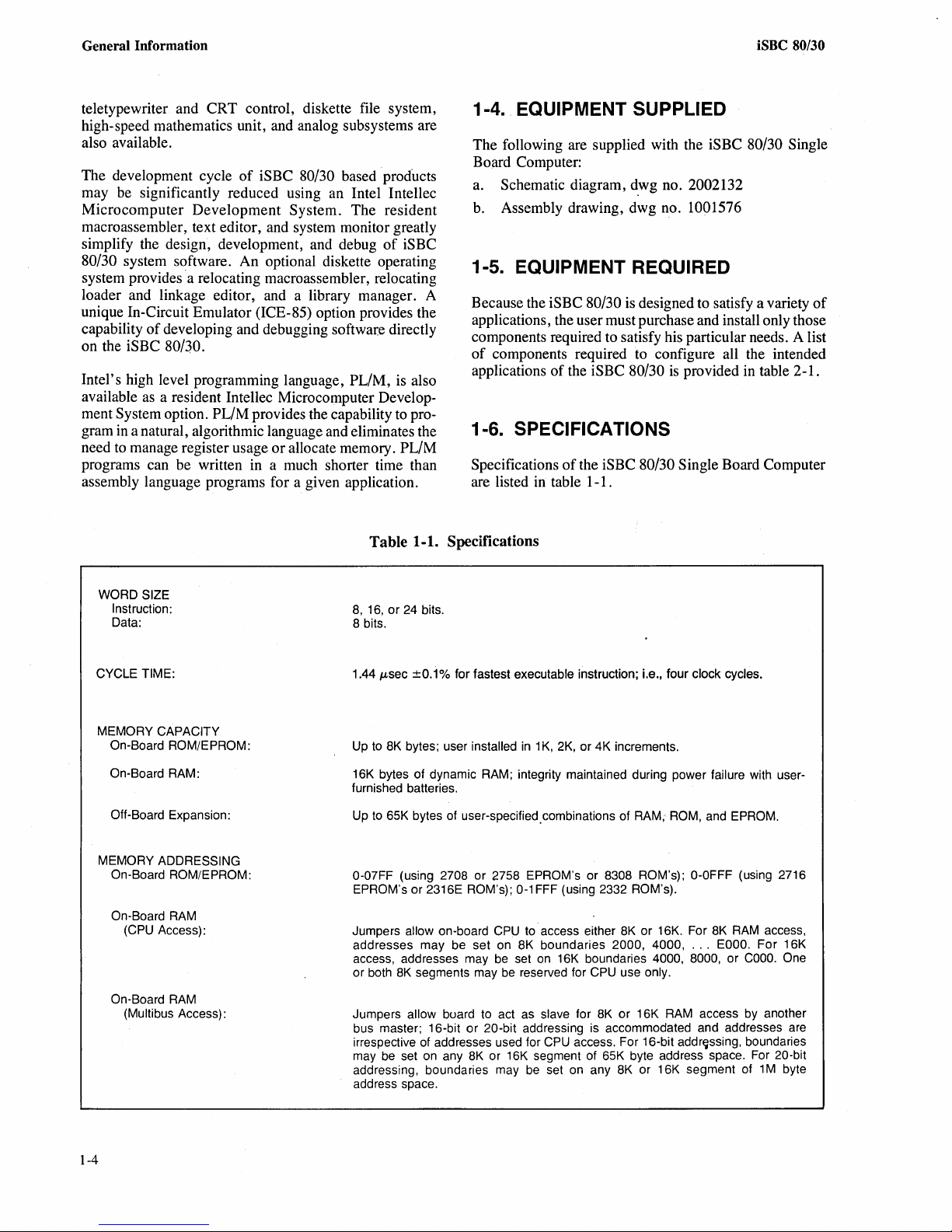
1-1. Specifications
1-4. EQUIPMENT SUPPLIED
The following are supplied with the iSBC 80/30 Single
Board Computer:
a. Schematic diagram,
b.
Assembly drawing, dwg no. 1001576
d,wg
no. 2002132
1-5. EQUIPMENT REQUIRED
Because the iSBC 80/30
applications, the user must purchase and install only those
components required to satisfy his particular needs. A list
of
components required to configure all the intended
applications
of
the iSBC 80/30
is
designed to satisfy a variety
is
provided in table 2-1.
of
1-6. SPECIFICATIONS
Specifications
are listed
of
the iSBC 80/30 Single Board Computer
in
table 1-1.
WORD SIZE
Instruction:
Data:
CYCLE
TIME:
MEMORY CAPACITY
On-Board ROMIE PROM:
On-Board RAM:
Off-Board Expansion:
MEMORY ADDRESSING
On-Board ROM/EPROM:
On-Board
On-Board
RAM
(CPU Access):
RAM
(Multibus Access):
8,
16,
or
24
8 bits.
1.44
Up
to
16K bytes of dynamic RAM; integrity maintained during power
furnished batteries.
Up
to
0-07FF
EPROM's or 2316E ROM's);
Jumpers
addresses may be set on 8K boundaries
access, addresses may
or both
Jumpers allow board to act as slave for
bus master; 16-bit or
irrespective
may
addressing, boundaries may
address space.
bits.
f.Lsec
±0.1 % for fastest executable instruction; i.e., four clock cycles.
8K bytes; user installed
65K bytes of user-specified.combinations of RAM,
(using 2708 or 2758 EPROM's or 8308 ROM's);
allow on-board
8K
segments may be reserved for CPU use only.
of
be
addresses used for
set
on
any
8K
in 1 K,
2K,
or 4K increments.
ROM,
0-1
FFF (using 2332 ROM's).
CPU
to· access either
be
set
on
16K boundaries 4000, 8000, or
20-bit addressing is accommodated and addresses are
or
CPU
16K
be
access. For 16-bit addrljssing, boundaries
segment of 65K byte address space. For 20-bit
set
on
8K
or 16K. For
2000, 4000,
8K
or 16K
any 8K or 16K segment of 1 M byte
RAM
O-OFFF
...
failure with user-
and EPROM.
(using 2716
8K
RAM
EOOO.
access by another
access,
For 16K
COOO.
One
1-4
Page 11
iSBC
80/30
SERIAL COMMUNICATIONS
Synchronous:
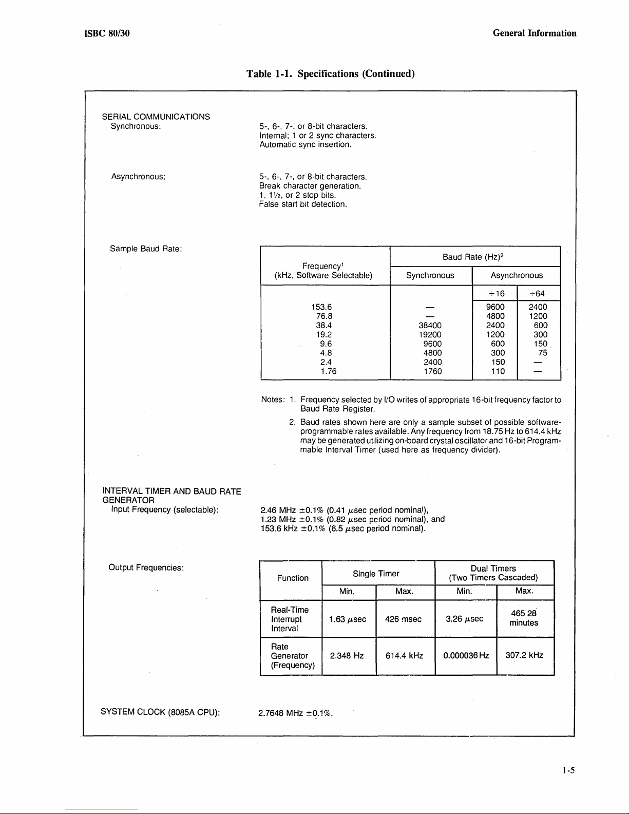
Table 1-1. Specifications (Continued)
S-,
6-, 7-, or 8-bit characters.
Internal; 1 or 2 sync characters.
Automatic sync insertion.
General Information
Asynchronous:
Sample Baud Rate:
5-, 6-, 7-, or 8-bit characters.
Break character generation.
1,
1
'12,
or 2 stop bits.
False start bit detection.
Frequency'
(kHz, Software Selectable)
153.6
76.8
38.4
19.2
9.6 9600 600 150
4.8
2.4
1.76
Notes:
1.
Frequency selected by
Baud Rate Register.
2.
Baud rates shown here are only a sample subset of possible softwareprogrammable rates available. Any frequency from 18.75 Hz to 614.4 kHz
may
be
generated utilizing on-board crystal oscillator and 16-bit Program-
mable Interval Timer (used here as frequency divider).
Baud Rate
Synchronous
-
-
38400
19200
4800 300
2400
1760
1/0
writes of appropriate 16-bit frequency factor to
(Hz)2
Asynchronous
+16
9600
4800 1200
2400
1200
150
110
2400
+64
600
300
75
-
-
INTERVAL
GENERATOR
Input Frequency (selectable):
Output Frequencies:
SYSTEM CLOCK (808SA CPU):
TIMER AND BAUD RATE
±0.1%
2.46 MHz
1.23 MHz ±0.1% (0.82
153.6 kHz
Function
Real-Time
Interrupt
Interval
Rate
Generator
(Frequency)
2.7648 MHz
(0.41
±0.1% (6.5
1.63/-L
2.348 Hz 614.4 kHz
±0.1%.
/-Lsec
period nominal),
/-Lsec
period nominal), and
/-Lsec
period nominal).
Single Timer
Min.
sec
Max.
426 msec
Dual Timers
(Two Timers Cascaded)
Min.
3.26/-Lsec
0.000036 Hz
Max.
46528
minutes
307.2 kHz
1-5
Page 12
General Information
iSBC 80/30
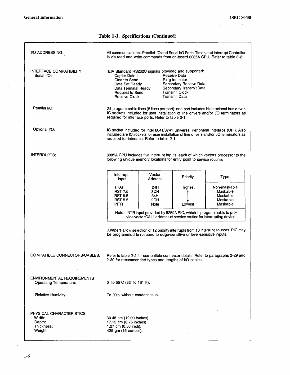
Table 1-1. Specifications (Continued)
I/O ADDRESSING:
INTERFACE COMPATIBILITY
Serial I/O:
Parallel I/O:
Optional I/O:
INTERRUPTS:
All communication
is via read and write commands from on-board 8085A CPU. Refer to table 3-2.
EIA Standard RS232C signals provided and supported:
Carrier Detect Receive Data
Clear to Send Ring Indicator
Data Set Ready Secondary Receive Data
Data Terminal Ready Secondary Transmit Data
Request to Send Transmit Clock
Receive Clock Transmit Data
24 programmable lines (8 lines per port); one port includes bidirectional bus driver.
IC sockets included for user installation of line drivers and/or I/O terminators as
required for interface ports. Refer to table 2-1.
IC socket included for Intel 8041/8741 Universal Peripheral Interface (UPI). Also
included are
required for interface. Refer to table 2-1.
8085A CPU includes five interrupt inputs, each of which vectors processor to the
following unique memory locations for entry point to service routine:
Interrupt Vector
Input
TRAP
RST
7.5
RST 6.5 34H
RST
5.5
INTR
to
Parallel I/O and Serial I/O Ports, Timer, and Interrupt Controller
IC
sockets for user installation of line drivers and/or I/O terminators as
Address
24H Highest
3CH
2CH
Note
Priority
Lowest
t
Type
Non-maskable
Maskable
Maskable
Maskable
Maskable
COMPATIBLE CONNECTORS/CABLES:
ENVIRONMENTAL REQUIREMENTS
Operating Temperature:
Relative Humidity:
PHYSICAL CHARACTERISTICS
Width:
Depth:
Thickness:
Weight:
Note:
INTR input provided by 8259A PIC, which
vide vector CALL address of service routine for interrupting device.
Jumpers
be programmed to respond to edge-sensitive or level-sensitive inputs.
Refer to table 2-2 for compatible connector details. Refer to paragraphs 2-29 and
2-30 for recommended types and lengths of I/O cables.
To
30.48
17.15
1.27 cm
425 gm (15 ounces).
allow selection of 12 priority interrupts from 18 interrupt sources. PIC may
90% without condensation.
cm
(12.00 inches).
cm
(6.75 inches).
(0.50 inch).
is
programmable to pro-
1-6
Page 13
iSBC 80/30
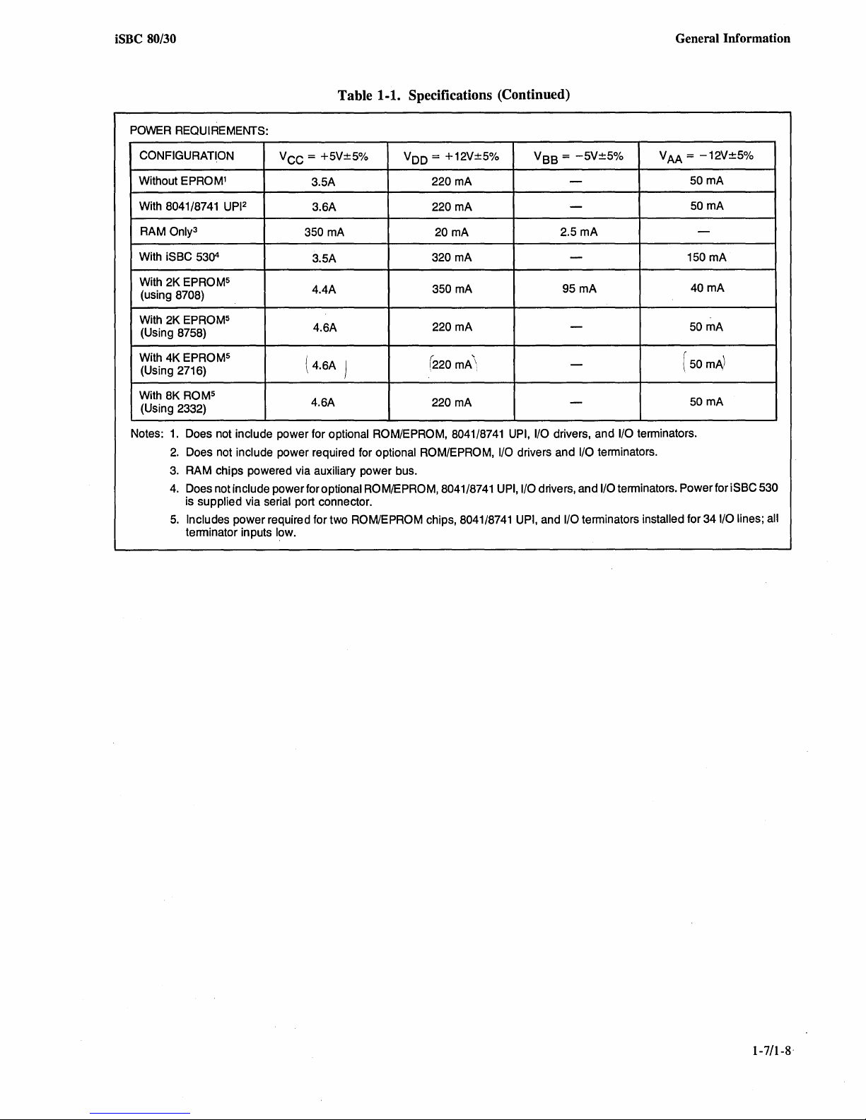
POWER REQUIREMENTS:
General Information
Table 1-1. Specifications (Continued)
CONFIGURATION
Without EPROM'
With 8041/8741
RAM Only3
With iSSC
With 2K EPROM5
(using
With 2K EPROM5
(Using 8758)
With 4K EPROM5
(Using 2716)
With 8K ROM5
(Using 2332)
Notes:
53Q4
8708)
1.
Does not include power for optional ROM/EPROM, 8041/8741 UPI, I/O drivers, and I/O terminators.
2.
Does not include power required for optional ROM/EPROM, I/O drivers and I/O terminators.
3.
RAM chips powered via auxiliary power bus.
4.
Does not include power for optional ROM/EPROM, 8041/8741 UPI, I/O drivers, and I/O terminators.
is supplied via serial port connector.
5.
Includes power required for two ROM/EPROM chips, 8041/8741 UPI, and I/O terminators installed for
terminator inputs low.
UPI2
Vce = +5V±5%
3.5A
3.6A 220 rnA
rnA 20 rnA
350
3.5A
4.4A
4.6A
(4.6A
!
4.6A 220 rnA
VD
=
D
220 rnA
+12V±5%
VSS = -5V±5%
-
-
2.5 rnA
320 rnA
350 rnA
220 rnA 50 rnA
(220 rnA
\,
-
95 rnA
-
-
-
VAA =
-12V±5%
SOmA
SOmA
-
150 rnA
40 rnA
(50
rnA)
50 rnA
PowerforiSSC530
341/0
lines; all
1-7/1-8'
Page 14
CHAPTER 2
PREPARATION FOR USE
2-1. INTRODUCTION
This chapter provides instructions for preparing the iSBC
Single Board Computer for use in the user-defined
80/30
It
environment.
1 and 3 be fully understood before beginning the configuration and installation procedures provided
chapter.
is advisable that the contents
of
Chapters
in
this
2-2. UNPACKING AND INSPECTION
Inspect the shipping carton immediately upon receipt for
of
evidence
carton
the carrier's agent be present when the carton
the carrier's agent
and the contents
carton and packing material for the agent's inspection.
For repairs to a product damaged in shipment, contact the
Intel Technical Support Center (see paragraph 5-4)
obtain a Return Authorization Number and further instructions. A purchase order will be required to complete
the repair. A copy
ted to the carrier with your claim.
mishandling during transit. .If the shipping
is
severely damaged or waterstained, request that
is
opened.
is
not present when the carton
of
the carton are damaged, keep the
of
the purchase order should be submit-
is
opened
If
to
Important criteria for installing and interfacing the
iSBC 80/30
following paragraphs.
in
the above environments are presented in
2-4. USER-FURNISHED COMPONENTS
Because the iSBC 80/30
applications, the user need purchase and install only those
components required to satisfy his particular configura-
tion. A list
intended applications
2-1. Table 2-2 lists details, types, and vendors
connectors referenced in table 2-1.
of
components required to configure all the
is
designed to satisfy a variety
of
the iSBC 80/30 are listed in table
of
of
those
2-5. POWER REQUIREMENTS
The iSBC 80/30 requires
power supply inputs. The currents required from these
supplies are listed in table 1-1. (The - 5 V supply is
mandatory only
an on-board regulator that operates off the
can otherwise supply the
if
+5V,
-5V,
+ 12V, and
Intel 2708 EPROM chips are installed;
-5V
power.)
-12V
-12V
supply.
2-6. COOLING REQUIREMENT
It is suggested that salvageable shipping cartons and packing material be saved for future use in the event the
product must be reshipped.
2-3. INSTALLATION CONSIDERATIONS
The iSBC 80/30 is designed for use in one
configurations:
a. Standalone (single-board) system.
b. Bus master in a single bus master system.
c. Bus master in a multiple bus master system.
of
the following
The iSBC 80/30 dissipates 401 gram-calories/minute
of
(1.62 Btu/minute) and adequate circulation
provided to prevent a temperature rise above 55°C
(131°F). The System
tem include fans to provide adequate intake and exhaust
ventilating air.
80 enclosures and the Intellec Sys-
air must be
of
2-7. PHYSICAL DIMENSIONS
Physical dimensions
a. Width:
b.
Height:
c. Thickness:
of
the iSBC 80/30 are as follows:
30.48 cm (12.00 inches).
17.15 cm (6.75 inches).
1.25 cm (0.50 inch).
2-1
Page 15
Preparation for
Use
iSBC
80/30
Item
No.
1
2
3
4
5 Connector
6
7
Item
iSBC 604 Modular Backplane and Cardcage. In-
iSBC 614 Modular Backplane and Cardcage. In-
Connector
{mates with
Connector
{mates with
{mates with J1}
Connector
{mates with J2}
Connector
{mates with J3}
Table 2-1. User-Furnished
Description
four slots with bus terminators.
cludes
{See figure 5-3.}
cludes
four slots without bus terminators.
{See figure 5-4.}
Multibus
P1}
P2}
See
table 2-2.
Auxiliary
See
table 2-2.
See parallel
table 2-2.
See parallel I/O connector details in
table 2-2.
See serial I/O connector details
table 2-2.
I/O
and
Installed Components
connector
connector details
connector details in
details
Use
Provides
signal interface between iSBC 80/30 and
three
system.
Provides four-slot
in
in
in
Power inputs
Not required if
in
Auxiliary backup battery inputs and associated memory protect functions.
Interfaces parallel I/O ports to Intel 8255A
Programmable Peripheral Interface {PPI}.
Interfaces I/O ports to optional Intel 8041/
8741A
{UPI}.
Interfaces serial I/O port to
Programmable Communications Interface
{USART}.
power input pins and Multibus
additional boards
extension of iSBC 604.
and
Multibus signal interface
an iSBC 604/q14.
iSBC 80/30
Universal
Peripheral
in
a multiple board
is
installed
Interface
Intel.
8251A
in
8
9
10
11
ROM/EPROM Chips One
ROM/EPROM chips:
ROM
8308
-
2316E 2716
2332
Intel 8041/8741 A
Line Drivers
I/O Terminators Intel iSBC
Universal Peripheral Interface {UPI}.
SN74031,OC
SN7400 I
SN7408
SN7409
Types
ing,
collector.
Pull-Up:
or
two
each of the following
EPROM
2708
2758
-
Type
NI
NI,
OC
selected as typical; I = invert-
NI
= noninverting, and OC = open
901
Divider or iSBC 902
iSBC
901
~
330
iSBC 902
0
1K x 8
2K
4K x 8
Current
16 rnA
16 rnA
16 rnA
16 rnA
220
l~~v
0
BITS
1K
Intel
x 8
x 8
On-board UV erasable PROM for program
development and/or dedicated program
Compatible ROM chips can also
use.
employed.
do not mix.
Single
memory,
timer,
faces two 8-bit I/O ports; two additional
input bits
branch and event timer functions.
Used for interface to
optional Intel 8041/8741. Requires two
line driver IC's for each 8-bit parallel
output port. {Exception: refer to paragraph 2-11.}
Used for interface
optional Intel 8041/8741A.
901
input port. {Exception: refer to paragraph
2-11.} Additional
8041/8741
for conditional branch
functions.
Use either ROM or EPROM;
chip microcomputer with program
I/O, and clock oscillator. Inter-
's or two 902's for each 8-bit parallel
memory,
data
{TO
and T1} for conditional
901
if
TO
and
CPU,
Intel 8255A and
to
Intel 8255A and
Requires two
or 902 required for
T1
inputs are used
or
event timer
be
event
12
2-2
Capacitors
Seven capacitors as required.
Rise time/noise capacitors for
port.
serial I/O
Page 16
iSBC 80/30
Table 2-2. User-Furnished Connector Details
Preparation for
Use
Function
Parallel
I/O 25/50
Connector
Parallel
I/O
Connector
Parallel
I/O
Connector
Serial
I/O
Connector
Serial
I/O 13/26
Connector
Serial
1/0
Connector
Multibus
Connector
No. Of
Palrsl
Pins (Inches) Type
25/50
25/50
13/26
13/26
43/86
Centers
0.1
0.1
0.1
0.1
0.1
0.1
0.156 Soldered
Connector
Flat Crimp
Soldered VIKING
Wirewrap1
Flat Crimp
Soldered
Wirewrap1
MICRO PLASTICS
1
Vendor
3M
3M
AMP
ANSLEY
SAE
AMP
TI
TI
VIKING
COC3
ITICANNON
3M
AMP 88106-1
ANSLEY 609-2615
SAE
TI
AMP
TI
COC3
ARCO
VIKING
3415-0000 WITH EARS
3415-0001 WID EARS
88083-1
609-5015
S06750
2-583485-6
3VH25/1JV5
H312125
H311125
3VH25/1
VPB01 B25000A 1
EC4A050A1A
3462-0001
S06726
H312113
1-583485-5
H311113
VPB01 E43000A 1
MP-0156-43-BW-4
AE443WP1 LESS EARS
2VH43/1AV5
Vendor Part No.
SERIES
JN05
SERIES
Intel
Part No.
iSBC 956
Cable
Set
N/A
N/A
955
iSBC
Cable
Set
N/A
N/A
N/A
Multibus
Connector
AUXiliary
Connector
Auxiliary
Connector
NOTES:
1.
2.
3.
43/86
30/60
30/60
Connector heights are not guaranteed to conform to OEM packaging equipment.
Wirewrap pin lengths are not guaranteed to conform to OEM packaging equipment.
CDC VPB01 ... , VPB02 ... , VPB04 ... , etc. are identical connectors with different electroplating thicknesses
surfaces.
0.156
0.1
0.1
Wirewrapl.2
Soldered
Wirewrapl.2
1
2-8. COMPONENT INSTALLATION
Instructions for installing the optional ROM/EPROM,
Intel 8041/8741A Universal Peripheral Interface, line
VO
drivers,
are given in following paragraphs. When installing the
optional chips, be sure to orient pin 1
the white dot located near pin 1
The grid location on figure 5
and figure 5 -2 (schematic diagram) are specified for each
user-installed component. Because the schematic
gram consists
terminators, and rise time/noise capacitors
of
the chip adjacent to
of
the associated IC socket.
-1
(parts location diagram) .
dia-
of
nine sheets, grid references to figure 5
...
COC3
COC3
VIKING
TI H312130
VIKING
COC3
TI
consist
of
VFB01 E43000A 1 or
VPB01
E43AOOA
2VH43/1AV5
3VH30/1JN5
VPB01
B30AOOA2
H311130
1
four alphanumeric characters. For example,
grid reference 6ZD4 signifies sheet 6 Zone D4.
2-9.
ROM/EPROM
cmps
Install the ROM/EPROM chips in IC sockets A25 and
-1
A37. (Refer to figure 5
zone ZC3 and figure 5 -2 zone
3ZA3.) Sockets A25 and A37, respectively,
modate the low order and high-order addresses
ROM/EPROM chip pair. For instance,
if
two Intel 2716
EPROM chips are installed, the chip installed in IC socket
A25 is assigned addresses
IC socket A37 is assigned addresses
2
0000-07FF; the chip installed in
0800-0FFF.
MOS 985
N/A
N/A
or
accom-
metal
of
the
2-3
Page 17
Preparation for
Use
iSBC 80/30
The default (factory connected) jumpers are configured
for Intel 2316E ROM
or
2716 EPROM.
If
different type
chips are installed, reconfigure the jumpers as described in
paragraph 2 -14.
2-10. UNIVERSAL PERIPHERAL
INTERFACE
Install the optional Inte18041/8741A Universal Peripheral
Interface (UPI) chip in socket A20. (Refer to figure 5-1
zone ZC6 and figure 5-2. zone 5ZC4.)
2-11. LINE DRIVERS AND 110
TERMINATORS
Table 2-3 lists the I/O ports and the location
sockets for installing either line drivers
(Refer
to
table 2
-1
items
10
and 11.) Port
equipped with Intel 8226 Bidirectional Bus Drivers and
requires no additional components. (Refer
2-22 and 2-23.)
of
associated IC
or
I/O terminators.
E8
is
factory
to
paragraphs
2-12. RISE TIME/NOISE CAPACITORS
Eye pads are provided so that rise time/noise capacitors
may be installed
pins. The selection
user and is normally a function
ment. The location
as
required on the individual serial I/O
of
capacitor values
of
these eye pads are
is
at the option
of
the particular environ-
as
follows:
of
the
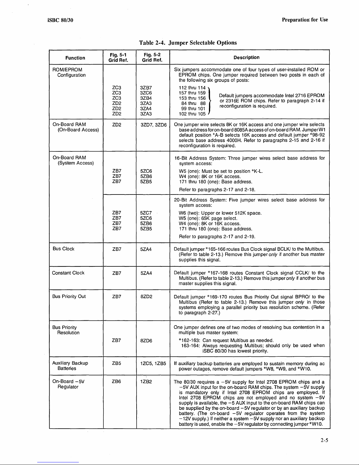
2-13. JUMPER CONFIGURATION
The iSBC 80/30 includes a variety
options to allow the user
to
parficular applicatio'n. Table
jumper-selectable options and lists
locations
of
the jumpers
as
location diagram) and figure 5-2 (schematic diagram).
Because the schematic consists
to
references
figure 5-2 consists
characters. For example, grid reference 3ZB7 signifies
sheet 3 Zone B7.
Study table 2-5 carefully while making reference to
figures 5-1 and 5-2.
If
the default (factory configured)
jumper wiring is appropriate for a particular function, no
further actions is required for that function.
different configuration
jumper(s) and install
is
required, remove the default
an
optional jumpers(s)
For most options, the information in table 2-4 is suffi-
cient for proper configuration. Additional information,
where necessary for clarity,
paragraphs.
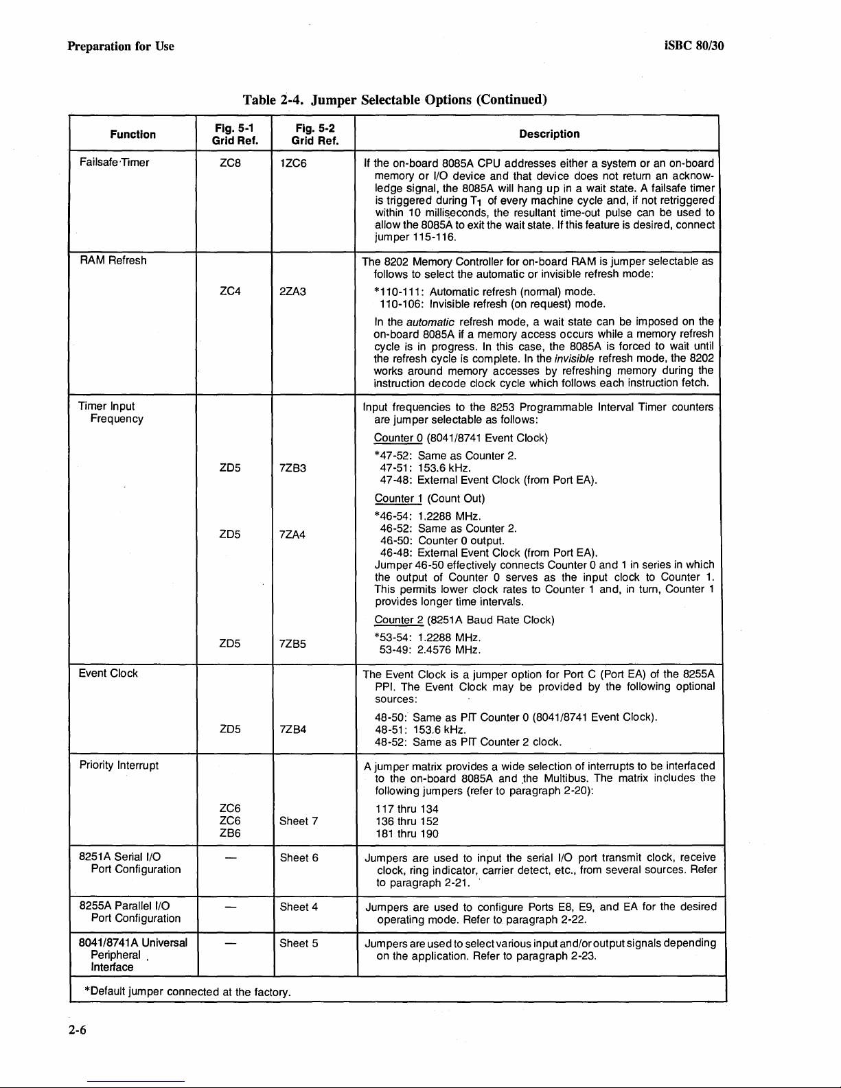
2-14. ROM/EPROM CONFIGURATION
Table 2-5 lists the jumper configurations and associated
address block for the various 'types
ROM/EPROM chips.
of
jumper-selectable
configure the board for his
2-4
summarizes these
the-
grid reference
shown
of
of
is
described
in
figure 5-1 (parts
nine sheets, grid
four alphanumeric
If,
however, a
as
specified.
in
subsequent
of
compatible Intel
Capacitor Fig.
C11
C12
C13
C14
C16
C17
C18
8255A
PPI
Interface
8041/8741
UPI
Interface
(Optional)
Z04
Z04 6Z83
Z03
Z04 6Z04
Z03 6Z06
Z03
Z03
5-1
Fig. 5-2
6Z04
6ZC4
6ZC6
6Z06
Table 2-3. Line Driver
1/0
Port
E8
E9
EA
1
2
Bits
0-7 None Required -
0-3
4-7
0-3
4-7
0-3
4-7
0-3
4-7
2-15. ON-BOARD RAM ADDRESSES
This on-board RAM can be accessed by the on-board
8085A microprocessor (CPU)
masters in the system via the
board 8085A access and for system access are assigned as
and
1/0
described in
Terminator Locations
Driver/
Terminator
A5
A6
A4
A3
A7
A8
A10
A11
paragraph~
Fig. 5·1
as
well as by other bus
~1ultibus.
Addresses for on-
2-16 and 2-17, respectively.
Fig. 5·2
Grid
Ref.
Z06
Z06
Z07
Z07
Z06
Z06
Z05 5Z83
Z05
Grid
4ZA3
4ZA3
4ZC3
4Z83
5Z03
5ZC3
5Z83
Ref
-
-
2-4
TO,
T1
A9
Z05
5ZC3
Page 18
iSBC 80/30
Preparation for
Use
Function
ROM/EPROM
Configuration
On-Board RAM
(On-Board Access)
On-Board
(System Access)
RA
M
Table 2-4.
5-1
Fig.
Grid Ref.
ZC3 3ZB7
ZC3 3ZC6 157 thru 159
ZC3
ZD2
ZD2
ZD2 3ZA3 102 thru 105
ZD2
ZB7
ZB7
ZB7
ZB7
ZB7
ZB7
ZB7
Fig. 5-2
Grid Ref.
3ZB4
3ZA3 84 thru
3ZA4
3ZD7,3ZD6
5ZC6
5ZB6
5ZB5
5ZC7
5ZC6
5ZB6
5ZB5
Jumper
Selectable Options
Six
jumpers accommodate one of four types of user-installed ROM or
EPROM chips.
the
following six groups of posts:
112
thru
153 thru 156
99
thru
One jumper wire selects
base address for on-board 8085A access of on-board RAM. JumperW1
default position *A-B selects 16K access and default jumper *98-92
selects base address 4000H. Refer
reconfiguration
16-Bit Address System: Three jumper wires
system access:
W5 (one): Must
W4 (one):
171
thru 180 (one): Base address.
Refer
to
20-Bit Address System: Five jumper wires
system access:
W6 (two): Upper or lower 512K space.
W5 (one): 65K page select.
W4 (one):
171
thru 180 (one): Base address.
Refer
to
Description
One
jumper required between two posts
114)
Default jumpers accommodate Intel 2716 EPROM
88
101
8K
paragraphs 2-17 and 2-18.
8K
paragraphs 2-17 and 2-19.
or 2316E ROM chips. Refer
reconfiguration
8K
or 16K access and one jumper wire selects
is
required.
be
set
to
or 16K access.
or 16K access.
position *K-L.
to
is
required.
to
paragraphs 2-15 and 2-16 if
paragraph 2-14
select base address for
select base address for
in
each of
if
Bus
Clock
Constant Clock
Bus
Priority Out
Bus Priority
Resolution
Auxiliary Backup
Batteries
On-Board
-5V
Regulator
ZB7
ZB7
ZB7 8ZD2
ZB7
ZB5
ZB6
5ZA4
5ZA4
8ZD6
1ZC5,1ZB5
1ZB2
Default jumper *165-166 routes Bus Clock signal BCLKI
(Refer
to
supplies this signal.
Default jumper *167-168 routes Constant Clock signal CCLK/ to the
Multibus. (Refer
master supplies this signal.
Default jum per * 169-170 routes Bus Priority Out signal BPRO/
Multibus (Refer to table 2-13.) Remove this jumper only
systems
to paragraph 2-27.)
One jumper defines one of two modes of resolving bus contention
multiple
*162-163:
If auxiliary
power outages, remove
The 80/30 requires a
-5V
is
Intel
supply is available, the
be
battery.
-12V
battery is used, enable the
table 2-13.) Remove this jumper only
to
table 2-13.) Remove this jumper only
employing a parallel priority bus resolution scheme. (Refer
bus master system:
Can
163-164:
AUX
mandatory only
2708 EPROM chips
supplied by the on-board
supply.)
request Multibus
Always requesting Multibus; .should only
iSBC 80/30 has lowest priority.
backup batteries are employed
input for the on-board RAM chips. The system
(The
-5V
if
on-board
If
neither a system
default jumpers *W8, *W9, and *W10.
Intel 2708 EPROM chips are employed. If
-5
as
needed.
to
sustain memory during ac
supply for Intel 2708 EPROM chips and a
are
not employed and
AUX
input
to
-5V
-5V
regulator operates from the system
-5V
regulator by connecting jumper*W10.
the on-board RAM chips can
regulator or by
-5V
supply nor
to
if
the Multibus.
another bus master
if
another bus
to
in
those
be
used when
-5V
supply
no
system
an
auxiliary backup
an
auxiliary backup
the
in
-5V
a
2-5
Page 19
Preparation for
Use
iSBC 80/30
Function
Failsafe Timer
RAM Refresh
Timer
Input
Frequency
Table 2-4.
5-1
Fig.
Grid Ref.
ZC8
ZC4
ZD5
ZD5
ZD5
Jumper
Fig. 5-2
Grid Ref.
1ZC6 If the on-board 8085A
2ZA3
7ZB3
7ZA4
7ZB5
Selectable Options (Continued)
or
memory
ledge signal, the 8085A will hang up
is triggered during
within 1
allow the 8085A
jumper 115-116.
The 8202 Memory
follows
*110-111: Automatic refresh (normal) mode.
110-106:
In
the automatic refresh mode, a wait state can
on-board 8085A if a memory access occurs while a memory refresh
cycle is
the refresh cycle
works around memory accesses by refreshing memory during the
instruction decode clock cycle which
frequencies
Input
are jumper selectable
Counter 0 (8041/8741 Event Clock)
*47-52:
47-51: 153.6 kHz.
47-48: External Event Clock (from Port EA).
Counter 1 (Count
*46-54: 1.2288 MHz.
46-52:
46-50: Counter 0 output.
46-48: External Event Clock (from Port EA).
Jumper 46-50 effectively connects Counter
the output of Counter
This permits lower clock rates
provides longer time intervals.
Counter 2 (8251A Baud Rate Clock)
*53-54: 1.2288 MHz.
53-49: 2.4576 MHz.
I/O device and that device does not return
0
milli~econds,
to
to
Controller for on-board RAM
select the automatic or invisible refresh mode:
Invisible refresh (on request) mode.
in
progress.
is
to
Same
as
Same
as
Description
CPU
addresses either a system or
in
T1
of every machine cycle and, if not retriggered
the resultant time-out pulse
exit
the
wait state. If this feature
In
this case, the 8085A is forced to wait until
complete.
the 8253 Programmable Interval Timer counters
Counter
Out)
Counter
as
follows:
2.
2.
0 serves
In
to
a wait state. A failsafe timer
is
jumper selectable
the invisible refresh mode, the 8202
follows each instruction fetch.
as
Counter 1 and,
0 and 1
the input clock
an
on-board
an
acknow-
can
be
is
desired, connect
be
in
in
used
imposed
series
in
to
Counter
turn, Counter 1
on
which
to
as
the
1.
Event Clock
ZD5
Interrupt
Priority
ZC6
ZC6
ZB6
8251A
Serial I/O
Port Configuration
8255A
Parallel I/O
Port Configuration
8041·/8741
*Default jumper connected at the factory.
A Universal
Peripheral.
Interface
- Sheet 6 Jumpers are used
- Sheet 4 Jumpers are used
- Sheet 5 Jumpers
2-6
7ZB4
Sheet 7
The Event Clock is a jumper option for Port
PPI. The Event Clock may
sources:
Same
as
48-50:
48-51: 153.6 kHz.
48-52:
Same
A jumper matrix provides a wide selection of interrupts to
to
the on-board 8085A and
following jumpers (refer
117 thru 134
136 thru 152
181
thru 190
clock, ring indicator, carrier detect, etc.,
to
paragraph 2-21.
operating mode. Refer
are
on the application. Refer
PIT
as
PIT
to
input the serial I/O port transmit clock, receive
to
configure Ports
used
to
select various input and/or output signals depending
be
provided by the following optional
Counter 0 (8041/8741 Event Clock).
Counter 2 clock.
,the
to
to.
Multibus. The matrix includes the
paragraph 2-20):
paragraph 2-22.
to
paragraph 2-23.
E8,
C (Port
EA)
from
several sources. Refer
E9,
and
EA
of
the 8255A
be
interfaced
for the desired
Page 20
iSBC 80/30
Preparation for
Use
Table 2-5.
ROM/EPROM
EPROM
EPROM
EPROM
*2316E
*Default jumpers are connected for type 2716 EPROM or
2316E ROM. Disconnect and reconfigure jumpers as
necessary if
2-16.
tion B-C allows the on-board
16K RAM; jumper
access to all 16K. For
may be configured on
EOOO;
configured on 16K boundaries
ROM/EPROM
Type
2708
or
8308
ROM
2758
*2716
or
ROM
2332
ROM
112-113,158-159,
100-101,104-105,
155-154, 86-84
112-113,158-159,
100-101,104-103,
155-154,86-87
112-113, 157-158,
100-101,104-103,
155-156,86-85
112-114,157-158,
100-99,104-102,
155-153,86-85
installing different type ROM/EPROM.
ON-BOARD808SAACCESS.
WI
SK
Configuration
Jumpers
Jumpers
Address
Block
0000-07FF
0000-07FF
OOOO-OFFF
0000-1 FFF
JumperWl
SOS5A
to access
SK
of
default position A-B allows
access, the RAM address block
SK
boundaries 2000, 4000,
posi-
the
...
for 16K access, the RAM address block may be
4000,
SOOO,
or
COOO.
(Address boundary 0000 is reserved for ROM/EPROM.)
Default jumper
and 16K access.
jumper
WI
B-C. If a different address boundary is desired,
9S
-92 selects boundary 4000 for both
If
only
SK
access is desired remove
from position A-B and install
it
id
position
SK
recon-
figure the jumpers as listed in table 2-6.
SYSTEM ACCESS. The on-board RAM can be
2-17.
shared by other bus masters in the system via the
Multibus.
If
one or more bus masters have a 20-bit
address capability, the extended addressing jumpers
allow the onboard RAM
I-megabyte address space. (The on-board
access memory in the
to
reside anywhere within a
lo~er
65K address space.) If it
SOS5A
can only
not desired to have the on-board RAM s4ared by the
system, leave default jumper
wise~
configure the jumpers for 16-bit addressing or
IS0-179 installed. Other-
20-bIt addressing as described in following paragraphs.
NOTE
Addresses for system access
are completely independent
board
SOS5A
access
of
of
on-board RAM
of
addresses for on-
on-board RAM.
Table 2-6.
Jumper
98-91
*98-92 4000-5FFF
98-93
98-94
98-95
98-96
98-97
NOTES:
1.
2.
3.
Jumper
808SA Access
Address block 0000-1 FFF is reserved for
ROM/EPROM.
Requires jumper
Requires jumper
*Default
is
required.
Configuration
of
On-Board
RAM Address
8KAccess
2000-3FFF
6000-7FFF
8000-9FFF
AOOO-BFFF
COOO-DFFF
EOOO-FFFF
jumper; disconnect if reconfiguration
2
W1
position B-C installed.
W1
position
for
RAM
Block1
16K Access
*A-B
2-18. 16-BIT ADDRESS SYSTEMS. For system access,
~n-board
the
1?~bIt
and Jumper W5 default position K-L restricts the
bIlIty
addresses
(Refer
As
shown
16K
~f
B-A lImIts the system to
B-C allows
RAM
is
divided into eight 65K pages. In
add~ess
to
systems, there
to
Page 0 (the only page in a 16-bit system).
is
no page selection capa-
table 2 -7.)
in
table 2-S, the system can access either
t~e
on-board RAM. Jumper W4 default
SK
access; jumper W4 position
acce!tS
of
all 16K
of
on-board RAM.
One jumper wire places the on-board RAM in the desired
SK
or
16K
segment
SK, for example, the
of
the selected 65K page. To access
SK
segment can be placed
boundary 0000 (1st SK), 2000 (2nd SK), 4000 (3rd
SK),
...
EOOO
(Sth SK). To access 16K, the 16K
segment can be placed on any 16K boundary
16K),
4000 (2nd 16K),
16K). Figure
2-1
SOOO
(3rd 16K), or
illustrates a step-by-step sequence for
establishing RAM addresses for 16-bit address systems.
is
2-19. 20-BIT ADDRESS SYSTEMS. In 20-bit address
systems, the on-board RAM can reside anywhere within a
As
I-megabyte address space.
RAM
is
first placed in the lower
W6. Jumper W5 then selects one
shown in table 2-7 the
or
upper 524K
of
eight 65K pages within
the upper or lower 524K bytes.
Next, referring to table 2-S, the system can access either
SK
or
16K
of
the on-board RAM. Default jumper W4
position B-A limits the system
position B-G allows access
of
all 16K
to
SK
access; jumper W4
of
on-board RAM.
On-Board
3
4000-7FFF
8000-BFFF
COOO-FFFF
installed.
SK
or
posi~ion
on
any
SI<
0000 (1st
COOOO
(4th
by
ju~per
2-7
Page 21
Preparation for
Use
iSBC 80/30
Table 2-7. 65K Page System Memory Selection
Low/(High)1
System
Memory
N/A
(Note
2)
0-524K
(525-1048K)
W6:
*B-C
*D-E
W6:
(B-E)
(D-A)
NOTES:
1. Notation in parentheses applies to high (upper
524K) bytes
Systems without 20-bit address capability must
2.
use jumper
* Default Jumper; disconnect if reconfiguration is
re~uired.
N/A
= not applicable.
65K
Page No.
0
W5:
*K-L
0
K-A
W5:
1 10000-1 FFFF
K-B
W5:
2 20000-2FFFF
K-C
W5:
3
K-D
W5:
4
K-E
W5:
5 50000-5FFFF
K-F
W5:
6 60000-6FFFF
K-G
W5:
7
K-H
W5:
of
20-bit system address space.
W5
in position
Address
OOOO-FFFF
OOOOO-OFFFF
(80000-8FFFF)
(90000-9FFFF)
(AOOOO-AFFFF)
30000-3FFFF
(BOOOO-BFFFF)
40000-4FFFF
(COOOO-CFFFF)
(DOOOO-DFFFF)
(EOOOO-EFFFF)
70000-7FFFF
(FOOOO-FFFFF)
*K-L.
Range
1
Table 2-8. 8K/16K Block Selection
Within
65K Page
Finally, one jumper wire places the on-board RAM in the
of
desired 8K or 16K segment
access an 8K segment in
the selected 65K page. To
Page 4
of
the lower 524K, for
example, the 8K segment can be placed on any 8K
boundary
(3rd 8K),
Page 4
in
placed on any 16K boundary
(2nd 16K), 48000 (3rd 16K),
40000
...
of
(l
st 8K), 42000 (2nd 8K),
4EOOO
(8th 8K). To access a 16K segment
the lower 524K, the 16K segment can be
40000
Ost
16K), 44000
or4COOO
(4th 16K). Figure
44000
2-2 illustrates a step-by-step sequence for establishing
RAM addresses for a
20-bit address system.
2-20. PRIORITY INTERRUPTS
Table 2-9 lists the source (from) and destination (to)
interrupt matrix shown in figure 5 -2 sheet 7. For example,
note that the 8259A Programmable Interrupt Controller
(PIC) can handle eight positive-true interrupt requests
and, after resolving any priority contention, outputs an
of
interrupt request to the INTR input
the 8085A micro-
processor.
Study table 2-9 carefully while making reference to figure
5-2 sheet 7 before deciding on a definite priority config-
uration for the
require some explanation: the 8085A
iSBC 80/30. There are two areas that
TRAP and RST 7.5
interrupts.
Default jumper 137-145 grounds the
input to prevent the possibility
generated by noise spikes.
of
Since the TRAP interrupt
TRAP interrupt
false interrupts being
maskable, cannot be disabled by the program, and has the
highest priority, it should be used only to detect a catastrophic event such
as
a power failure or a bus failure.
of
is
the
not
Address Block Within 65K
8K
or
W4:
W4:
16K
8K
*B-A
16K
B-C
System Access
*Default jumper; disconnect if reconfiguration is desired.
Page (Refer
Jumper
180-172 1st 8K
180-173 2nd 8K
180-174 3rd 8K
180-175 4th 8K
180-176 5th 8K
180-177 6th 8K
180-178 7th 8K
180-179
*180-171 No Access
180-173 1st 16K
180-175 2nd 16K
180-177 3rd 16K
180-179 4th 16K
*180-171
2-8
to
Table 2-7)
8th 8K
No Access
Block
The
RST 7.5 interrupt input
default jumpered to the COUNT OUT output
1.
If
it
is
desired to interrupt the 8085A if the Failsafe
Timer times out, remove jumper 123-138
is
edge-sensitive only and
of
(COUNT OUT)
Counter
and connect jumper 122-138 (BUS TIME OUT). (The
BUS TIME OUT signal
Timer
is
retriggered after timing out.)
is
generated when the Failsafe
NOTE
The 8259A PIC can be programmed to respond
or
to either edge-sensitive
If
rupt requests.
the PIC
level-sensitive inter-
is
programmed to re-
spond to edge-sensitive interrupt requests, the
PIC will respond only to a low-to-high transition
on
anyone
of
the individual IR input lines.
is
Page 22
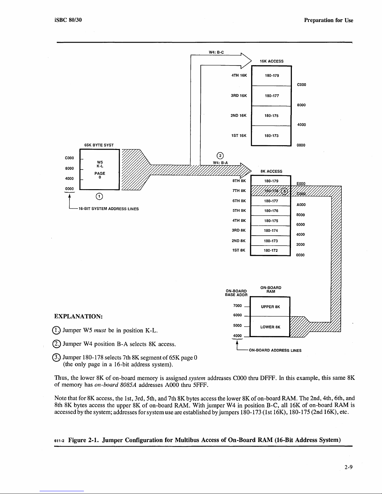
iSBC 80/30
65K
BYTE
SYST
W4:
B·C
4TH
3RD
2ND
1ST
16K
16K
16K
16K
16K
1 BO-175
1 BO-173
ACCESS
1 BO-179
1BO-177
Preparation for
COOO
BOOO
4000
0000
Use
COOO
-
BOOO
-
4000
0000
PAGE
-
--
L 16.BIT
EXPLANATION:
CD
Jumper W5 must be
SYS~EM
W5
K·L
0
CD
ADDRESS UNES
in
position K-L.
0
6TH
BK
5TH BK
4TH BK
3RDBK
2ND
BK
1ST
BK
ON·BOARD
BASE
AD
7000
6000
5000
4000
DR
----I
_____
BK
ACCESS
160-176
1BO-175
1BO-174
1BO-173
1
BO-172
ON·BOARD
RAM
UPPER BK
LOWER BK
AOOO
BOOO
6000
4000
2000
0000
...a:.LL..I.~
® Jumper W4 position B-A selects
® Jumper lS0-17S selects 7th
(the only page in a 16-bit address system).
Thus, the lower
of
memory has on-board 808SA addresses
Note that for
Sth
SK
bytes access the upper
accessed by the system; addresses for system use are established by jumpers
611-2
Figure 2-1.
SK
of
on-board memory
SK
access, the 1st, 3rd, 5th, and 7th
Jumper
Configuration for Multibus Access of On-Board RAM (16-Bit Address System)
SK
access.
SK
segment
SK
of
of
65K page 0
is
assigned system addresses
AOOO
thru 5FFF.
SK
bytes access the lower
on-board RAM. With jumper W4 in position B-C, all 16K
L
COOO
SK
ON·BOARD
thru DFFF.
of
on-board RAM. The 2nd, 4th, 6th, and
lS0-173 (1st 16K), lS0-175 (2nd 16K), etc.
ADDRESS
LINES
In
this example, this same
of
on-board RAM is
SK
2-9
Page 23
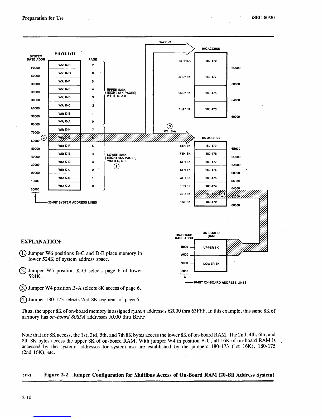
Preparation for
SYSTEM
BASE
AD
FOOOO
EOOOO
00000
COOOO
BOOOO
AOOOO
90000
80000
70000
60000
50000
40000
30000
20000
10000
00000
DR
0
Use
1M BYTE SYST
W5:K·H
W5:K·G
W5:
K·F
W5:
K·E
W5:K·D
W5:K·C
W5:K·B
W5:K·A
W5:
K·E
W5:K·D
W5:K·C
W5:K·B
W5:K·A
-
L 20·BIT SYSTEM ADDRESS LINES
PAGE
7
6
5
4
3
2
0
4
3
2
0
UPPER 524K
(EIGHT 65K PAGES)
W6:
B·E,
D·A
LOWER 524K
65K PAGES)
(EIGHT
W6:
B·C,
D·E
0)
W4:B·C
4TH 16K
3RD16K
2ND16K
1ST16K
7TH
8K
6TH
8K
5TH
8K
4TH
8K
3RD8K
2ND
8K
1ST8K
16K
180·179
180·177
180·175
180·173
8K
180·179
180·178
180·177
180·176
180·175
180·174
iSBC 80/30
ACCESS
6COOO
68000
64000
60000
ACCESS
6EOOO
6COOO
6AOOO
68000
66000
60000
ON.BOARD ON·BOARD
BASE
ADDR
.....
__
EXPLANATION:
BOOO
CD
Jumper W6 positions B-C and D-E place memory in
lower 524K
of
system address space.
® Jumper W5 position K-G selects page 6
524K.
® Jumper W4 position B-A selects
@Jumper
Thus, the upper 8K
memory has on-board
Note that for
Bth
IBO-173
selects 2nd
of
BK
access, the
BK
bytes access the upper
on-board memory is assigned system addresses 62000 thru 63FFF. In this example, this same
BOB5A
Ist,3rd,
BK
access
of
BK
segment
addresses
of
AOOO
5th, and 7th
BK
of
on-board RAM. With jumper W4
of
lower
page 6.
page 6.
thru BFFF.
BK
bytes access the lower
AOOO
~-----~F-""~V
9000
8000 .....J
______
T
L16.BIT
BK
of
on-board RAM. The 2nd, 4th,
in
position B-C, all 16K
accessed by the system; addresses for system use are established by the jumpers
(2nd 16K), etc.
611·3
Figure 2·2.
Jumper
Configuration for Multibus Access of On-Board RAl\1 (20-Bit Address System)
~A_M
__
UPPER
8K
LOWER
8K
ON·BOARD
IBO-173
-.-:77777'1o.
.....
ADDRESS
UNES
of
on-board RAM is
(lst
16K),
BK
of
6th~
and
IBO-175
2-10
Page 24
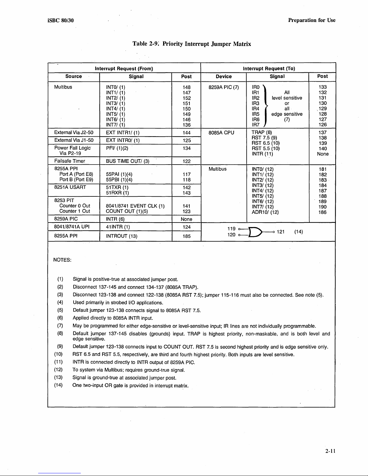
iSBC 80/30
Table 2-9; Priority Interrupt Jumper Matrix
Preparation for
Use
Source
Multibus
External Via J2-50
External Via J1-50
Power
Fail
logic'
P2-19
Via
Failsafe Timer
PPI
8255A
Port A (Port
Port
8251A USART
8253
PIT
Counter
Counter 1
8259A
8041/8741A
8255A
B (Port
0 Out
PIC
PPI
E8)
E9)
Out
UPI
Interrupt
Request (From)
INTO/
(1)
INT1/
(1)
INT2/
(1)
INT3/
(1)
INT4/
(1)
INT5/
(1)
INT6/
(1)
INT7/
(1)
EXT
INTR1/
EXT
INTRO/
PFI/ (1)(2)
BUS
TIME OUT/
55PAI
(1
55PBI
(1
51TXR
51RXR
8041/8741 EVENT
COUNT OUT
INTR
(6)
41INTR(1)
INTROUT (13)
)(4)
)(4)
(1)
(1)
Signal
(1)
(1)
(1
(3)
)(5)
elK
(1)
Post Device
148 8259A PIC
147
152
151
150
149
146
136
144 8085A
125
134
122
117
118
142
143
141
123
None
124
185
Multibus
CPU
119
120
Interrupt
(7)
IRO
'
IR1
IR2
IR3
IR4
IR5
IR6
IR7
TRAP
RST 7.5
RST 6.5
RST 5.5
(1.1)
INTR
INTO/
INT1/
INT2I
INT3/
INT4/
INT5/
INT6/
INT7/
ADR10/
Request (To)
>
(8)
(12)
(12)
(12)
(12)
(12)
(12)
(12)
(12)
:=D---o
Signal
All
level sensitive
or 130
all
edge sensitive
(7)
(9)
(10)
(10)
(12)
121
(14)
Post
133
132
131
129
128
127
126
137
138
139
140
None
181
182
183
184
187
188
189
190
186
NOTES:
(1)
(2)
(3)
(4)
(5)
(6)
(7)
(8)
(9)
(10)
(11)
(12)
(13)
(14)
Signal
is
positive-true at associated jumper post.
Disconnect 137-145 and connect 134-137 (8085A TRAP).
Disconnect 123-138
Used
primarily
Default jumper 123-138 connects signal
Applied directly
May
be
programmed for either edge-sensitive or level-sensitive input;
Default jumper 137-145 disables (grounds) input. TRAP
edge sensitive.
Default jumper 123-138 connects input to COUNT OUT. RST 7.5
RST 6.5 and RST
INTR
is
connected directly
To system via Multibus; requires ground-true signal.
Signal
is
ground-true at associated jumper post.
One two-input OR gate
and
connect 122-138 (8085A RST 7.5); jumper 115-116 must also
in
strobed
I/O
applications.
to
8085A RST 7.5.
to
8085A INTR input.
is
highest priority, non-maskable, and
5.5,
respectively, are third and fourth highest priority. Both inputs are level sensitive.
to
INTR output of 8259A
is
provided
in
interrupt matrix.
PIC.
be
connected. See note (5).
IR
lines are not individually programmable.
is
second highest priority and
is
is
both level and
edge sensitive only.
2-11
Page 25
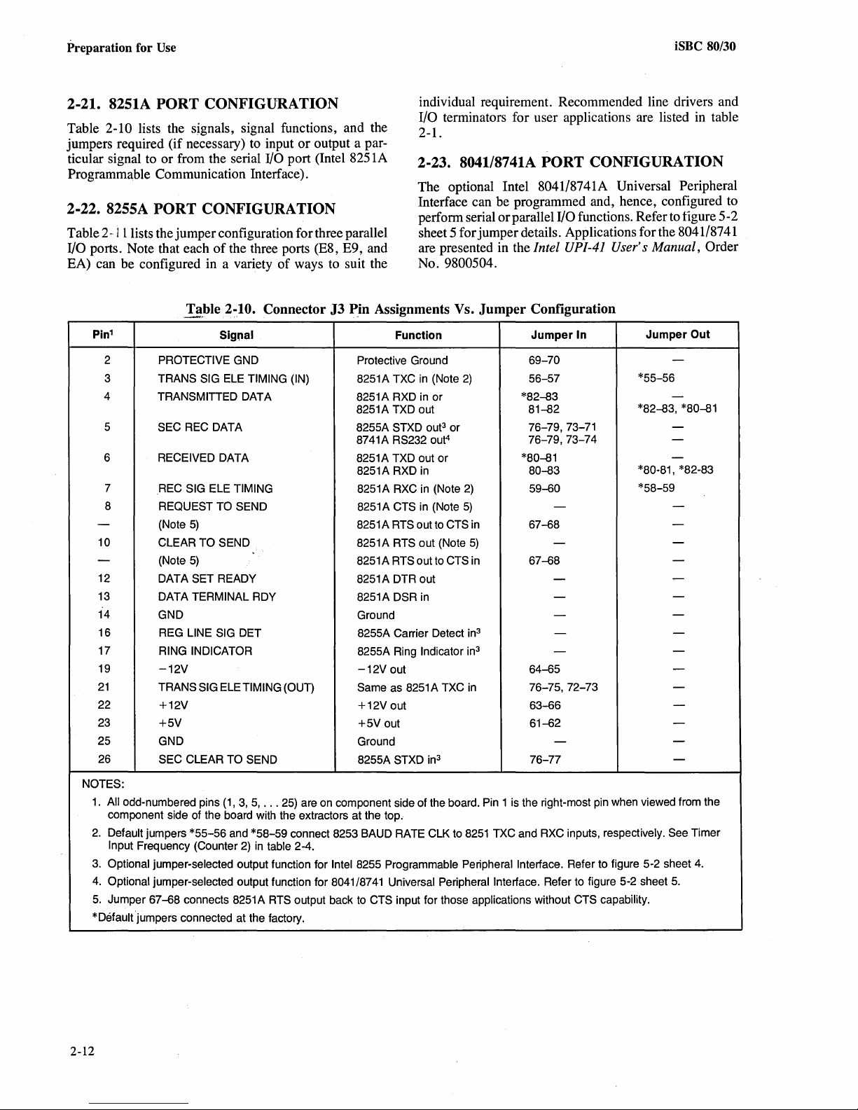
Preparation for
Use
iSBC 80/30
2-21. 8251A
PORT
CONFIGURATION
Table 2-10 lists the signals, signal functions, and the
jumpers required (if necessary)
ticular signal to or from the serial
to
input
or
output a par-
I/O port (Intel 8251A
Programmable Communication Interface).
2-22. 8255A
PORT
CONFIGURATION
Table 2··/ 1 lists the jumper configuration for three parallel
I/O ports. Note that each
EA) can be configured in a variety
1
Pin
2
3
4
5
6 RECEIVED DATA
7
8
PROTECTIVE GND
TRANS
TRANSMITTED DATA 8251A RXD in or
SEC REC DATA
REC
REQUEST
- (Note
10
-
12
13
14
16
17
19
21
22
23
25
26
CLEAR TO SEND 8251A RTS out (Note
(Note
DATA SET READY
DATA
GND
REG LINE
RING INDICATOR
-12V
TRANS SIG
+12V
+5V
GND
SEC CLEAR TO SEND
of
the three ports (E8, E9, and
of
ways
to
suit the
Table 2-10. Connector
Sigoal Function
SIG
ElE
TIMING (IN) 8251A TXC
SIG
ElE
TIMING
TO SEND
5)
5)
TERMINAL
ROY
SIG
DET
ElETIMING
(OUT)
J3
~in
Protective Ground
8251A TXD out
8255A STXD
8741A
8251A TXD out or *80-81
8251A RXD in
8251A RXC in (Note
8251A
8251A RTS out to CTS in 67-68
8251A RTS out to CTS in
8251A DTR out
8251A DSR in Ground
8255A Carrier Detect
8255A Ring Indicator
-12Vout
Same as 8251A TXC
+12Vout
+5Vout
Ground
8255A STXD
Assignments Vs.
individual requirement. Recommended line drivers and
I/O terminators for user applications are listed
2-1.
2-23. 8041/8741A
PORT
CONFIGURATION
The optional Intel 8041/8741A Universal Peripheral
Interface can be programmed and, hence, configured to
perform serial or parallel
I/O functions. Refer
to
sheet 5 for jumper details. Applications for the 8041/8741
are presented in the
Intel UPI-41 User's Manual, Order
No. 9800504.
in
(Note
ouP or
RS232 out
Jumper
2)
4
Configuration
Jumper
69-70
56-57
*82-83
81-82
76-79, 73-71
76-79,
In
73-74
Jumper
-
*55-56
-
*82-83, *80-81
-
-
-
*80-81, *82-83
*58-59
-
CTS in (Note
2)
5)
80-83
59-60
-
-
5)
-
67-68
-
-
-
-
-
-
3
in
3
in
in
-
-
64-65
76-75, 72-73
63-66
61-62
-
3
in
76-77
-
-
-
-
-
-
-
-
-
in
table
figure 5 -2
Out
NOTES:
1.
All odd-numbered pins
component side of the board with the extractors at the top.
2.
Default jumpers
Input Frequency (Counter
3.
Optional jumper-selected output function for Intel 8255 Programmable Peripheral Interface. Refer to figure 5-2 sheet
Optional jumper-selected output function for 8041/8741 Universal Peripheral Interface. Refer to figure 5-2 sheet
4.
Jumper
5.
* Default jumpers connected at the factory.
2-12
67-68
(1,
3,
5,
...
25) are on component side of the board. Pin 1
*55-56
and
*58-59
2)
in
table 2-4.
connects 8251A RTS output back
connect 8253 BAUD RATE
to
CTS input for those applications without CTS capability.
ClK
is
the right-most pin when viewed from the
to
8251
TXC and RXC inputs, respectively. See Timer
4.
5.
Page 26
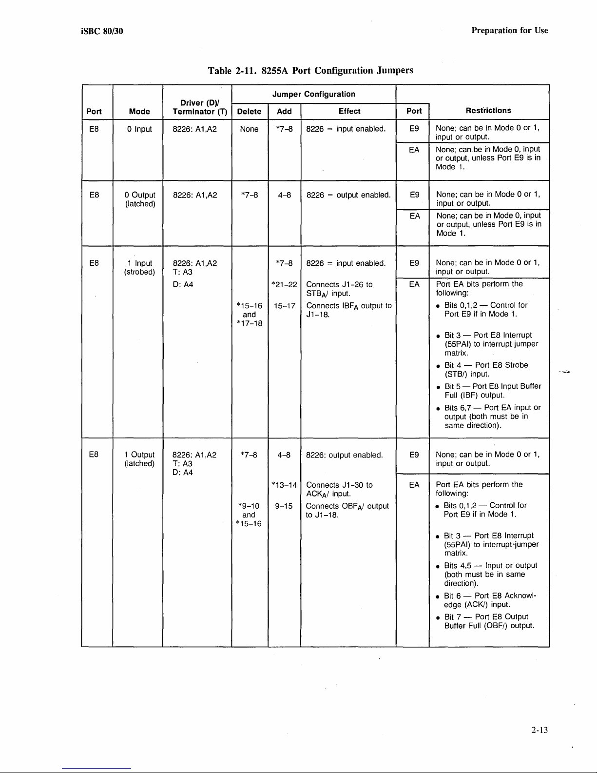
iSBC 80/30
Preparation for
Use
Port
E8
E8
E8
Table 2-11. 8255A
Mode
Driver (0)/
Terminator
(T)
Delete Add
o Input 8226: A1,A2 None
o Output
(latched)
1 Input
(strobed)
8226: A1,A2
8226: A1,A2
T:A3
D:A4
*7-8
*15-16
and J1-18.
*17-18
Port
Jumper
*7-8
4-8
*7-8
*21-22
15-17
Configuration
Configuration
Effect
8226 = input enabled.
8226 = output enabled.
8226 = input enabled.
Connects J1-26 to
STBAI input.
Connects
IBF
Jumpers
A output
Port
None;
E9
input or output.
None;
EA
or output,
Mode
E9
EA
None;
E9
input or output.
Port EA bits perform the
EA
following:
to
• Bits 0,1,2 - Control for
• Bit 3 - Port E8 Interrupt
• Bit 4 - Port E8 Strobe
• Bit 5 - Port E8 Input Buffer
• Bits 6,7 - Port
Rest'rictions
can
be
in
Mode 0 or
can
be
in
Mode
unless Port
1.
None; can
input or output.
None;
or output,
Mode
Port
(55PAI)
matrix.
(STB/)
Full (IBF) output.
output (both must be
same direction).
be
can
be
unless Port
1.
can
be
E9
if
in
to
interrupt jumper
input.
in
Mode 0 or
in
Mode
in
Mode 0 or
Mode
EA
0,
input
E9
is
0,
input
E9
is
1.
input or
in
1,
in
1,
in
1,
E8
1 Output
(latched)
8226: A1,A2
T:A3
D:A4
*7-8
*9-10
and
*15-16
4-8
*13-14
9-15
8226: output enabled.
Connects J1-30 to
ACKAI input.
Connects OBF
to
J1-18.
AI
output
None;
can
E9
be
if
to
E9
input or output.
Port EA bits perform the
EA
following:
• Bits 0,1,2 - Control for
Port
• Bit 3 - Port
(55PAI)
matrix.
• Bits 4,5 - Input or output
(both must be
direction).
• Bit 6 - Port E8 Acknowledge (ACK/) input.
• Bit 7 - Port
Buffer Full (OBF/) output.
in
Mode 0 or
in
Mode
1.
E8
Interrupt
interrupt ·jumper
in
same
E8
Output
1,
2-13
Page 27
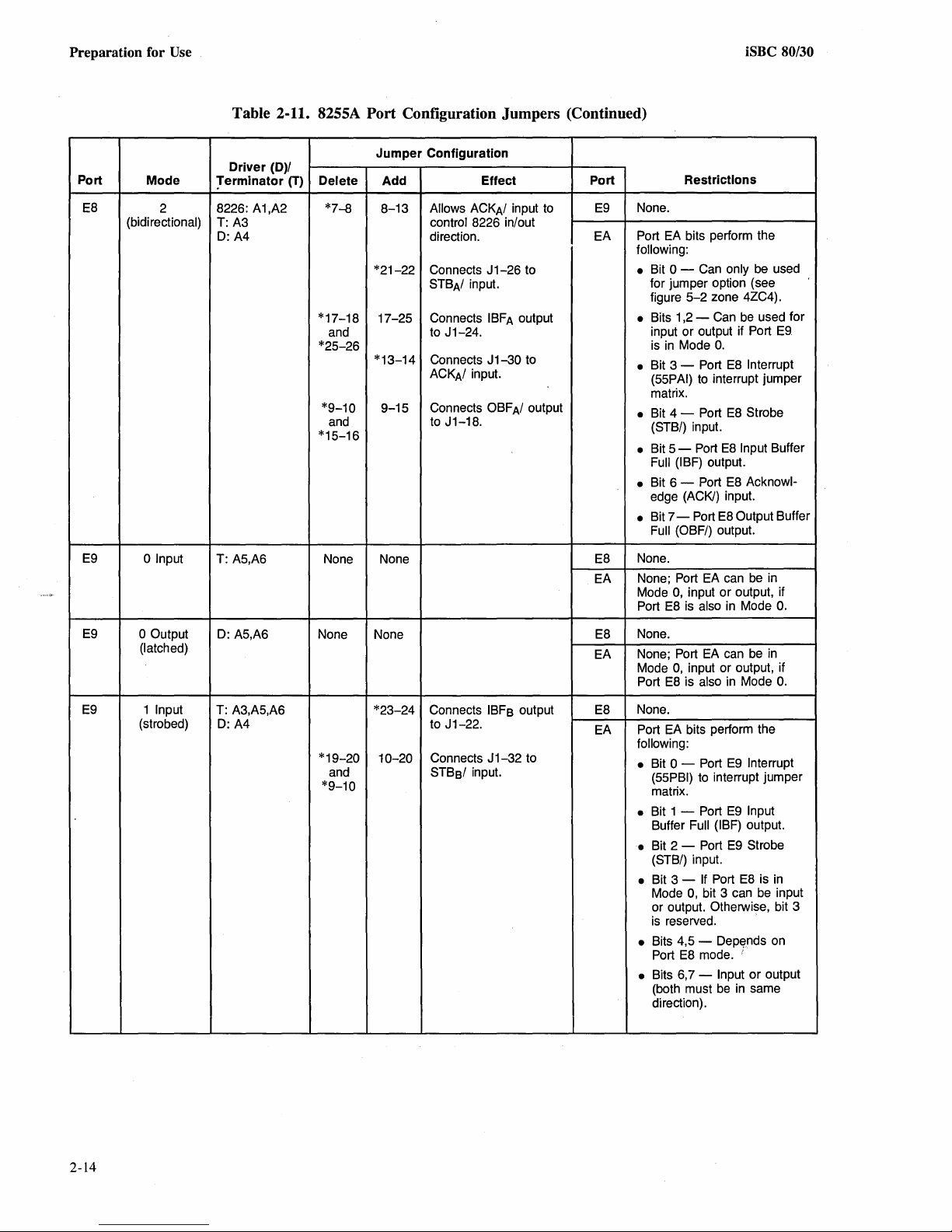
Preparation for Use
iSBC 80/30
Table 2-11. 8255A Port Configuration Jumpers (Continued)
Port
EB
E9
Mode
2 B226: A1,A2
(bidi
rectional)
o Input
Driver
(D}I
:rerminator
T:A3
D:A4
T: A5,A6
Jumper
Delete
(T)
*7-8
*17-1B
and to J1-24.
*25-26
*9-10
and
*15-16
None
Add
B-13 Allows ACKAI input
*21-22
17-25
*13-14
9-15
None
Configuration
Effect
control B226 in/out
direction.
Connects
STBAI input.
Connects
Connects
ACKA/
Connects OBFA/ output
to
J1-26
IBFA
J1-30
input.
J1-1B.
to
to • Bit 0 -
output
to
Port
E9
EA
EB
EA
Restrictions
None.
Port
EA
following:
• Bits 1
• Bit 3 - Port
• Bit 4 - Port
• Bit 5 - Port
• Bit 6 - Port
• Bit 7 - Port
None.
None; Port EA can
Mode
Port
bits perform the
Can
for jumper option (see
figure
input or output if
is
in
(55PAI)
matrix.
(STB/) input.
Full (IBF) output.
edge (ACK/) input.
Full (OBF/) output.
0,
EB
only
5-2
zone 4ZC4).
,2
- Can
Mode
O.
EB
to
interrupt jumper
EB
EB
EB
EB
Output Buffer
input or output, if
is also
in
be
used
be
used for
Port
E9
Interrupt
Strobe
Input Buffer
Acknowl-
be
in
Mode
O.
E9
E9
o Output
(latched)
1 Input
(strobed)
D:
A5,A6
T: A3,A5,A6
D:A4
None None
*23-24
*19-20
and
*9-10
10-20
Connects IBFs output
to J1-22.
Connects J
STBsI input.
1-32
to
None.
EB
None;
Port
EA
Mode
Port
None.
EB
Port EA bits perform the
EA
following:
• Bit 0 - Port
(55PBI)
matrix.
• Bit 1 - Port
Buffer Full (IBF) output.
• Bit 2 - Port
(STB/) input.
• Bit 3 Mode
or output. Otherwise, bit 3
is
• Bits 4,5 -
Port
• Bits 6,7 - Input or output
(both must
direction).
EA
0,
input or output, if
EB
is also
to
If
0,
bit 3 can
reserved. .
EB
mode.
can
be
in
in
Mode
O.
E9
Interrupt
interrupt jumper
E9
Input
E9
Strobe
Port
EB
is
in
be
input
Dep~nds
be
!
in
on
same
2-14
Page 28
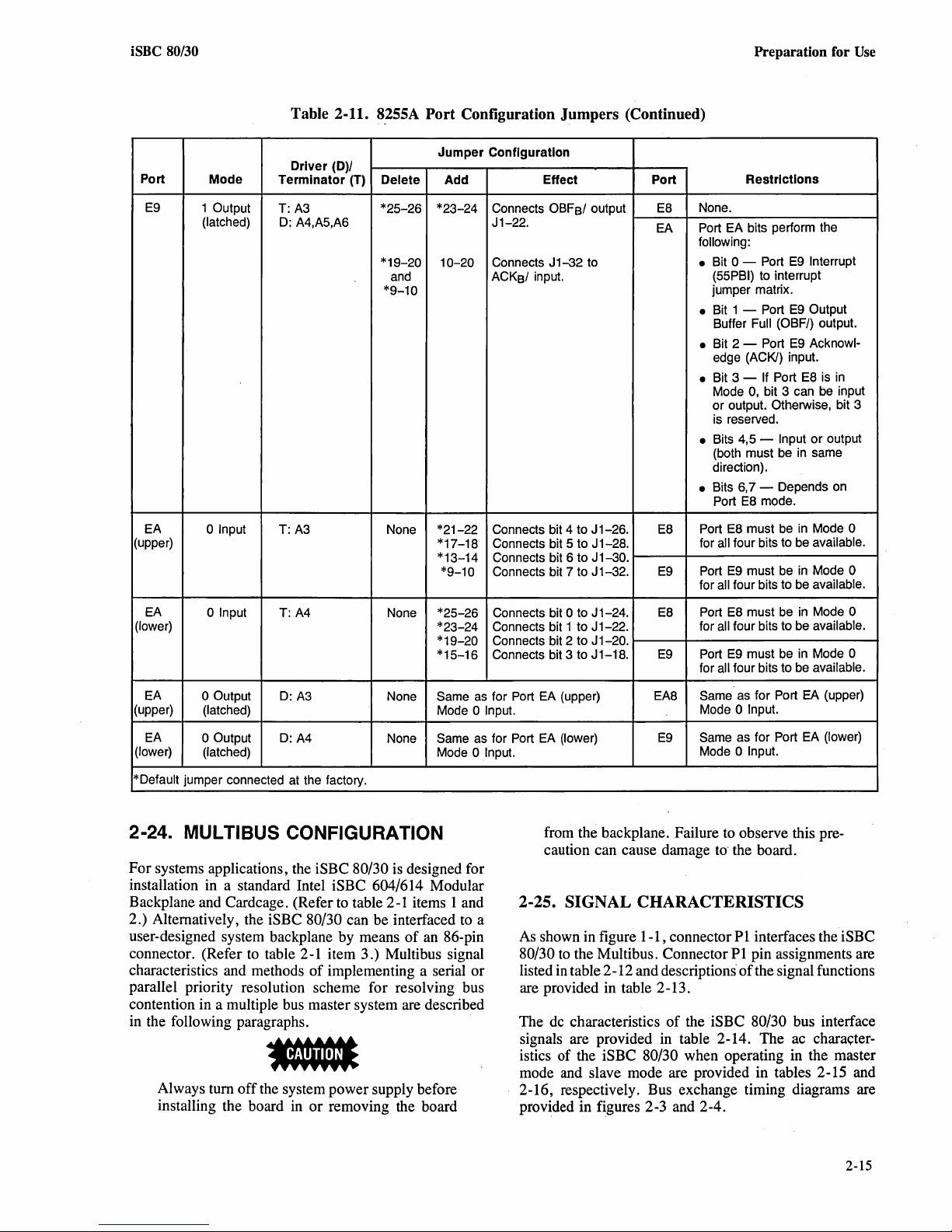
iSBC
80/30
Preparation for
Use
Port
E9
EA
(upper)
Mode
1 Output
(latched)
o Input
Table 2-11.
Driver
Terminator
T:A3
D:
T:A3
(D)/
A4,AS,A6
8.255A
(T)
Port Configuration Jumpers (Continued)
Jumper
Delete Add Effect Port
*25-26 *23-24
*19-20
and
*9-10
None
10-20
*21-22
*17-1B
*13-14
*9-10
Configuration
Connects OBFs/ output
J1-22.
Connects
ACKs/ input.
Connects bit 4 to J 1-26.
Connects bit
Connects bit 6 to J 1-30.
Connects bit 7 to J 1-32.
J1-32
S to J 1-2B.
to
Restrictions
None.
EB
Port EA bits perform the
EA
following:
• Bit 0 - Port
(SSPBI)
jumper matrix.
• Bit 1 - Port
• Bit 2 - Port
edge (ACKI) input.
• Bit 3 - If Port
Mode
or output. Otherwise, bit 3
is reserved.
• Bits 4,5 - Input
direction).
• Bits 6,7 - Depends on
Port
EB
for all four bits to be available.
Port
E9
for all four bits to
to
Buffer Full (OBF/) output.
0,
bit 3 can
(both must be
Port
EB
mode.
EB
must
E9
must be
E9
Interrupt
interrupt
E9
Output
E9
Acknowl-
EB
or
in
be
in
in
be
is
in
be
input
output
same
Mode 0
Mode 0
available.
EA
(lower)
EA
(upper)
EA
(lower)
*Default
o Input
o Output
(latched)
o Output
(latched)
jumper connected
T:A4
D:
A3
D:A4
at
the factory.
None
None Same
None Same
*2S-26
*23-24
*19-20
*1S-16
Mode 0 Input.
Mode
as
as
0 Input.
2-24. MUL TIBUS CONFIGURATION
For systems applications, the iSBC 80/30
installation in a standard Intel
Backplane and Cardcage. (Refer
2.) Alternatively, the
iSBC 80/30 can be interfaced to a
iSBC 604/614 Modular
to
user-designed system backplane by means
to
table 2
-1
connector. (Refer
characteristics and methods
item 3.) Multibus signal
of
implementing a serial
parallel priority resolution scheme for resolving bus
contention in a mUltiple bus master system are described
in the following paragraphs.
is
designed for
table 2-1 items 1 and
of
an 86-pin
or
..
Always tum off the system power supply before
or
installing the board in
removing the board
Connects bit 0 to J 1-24.
Connects bit 1 to J 1-22.
Connects bit 2 to J1-20.
Connects bit 3 to J 1-1B.
for Port EA (upper)
for Port EA (lower)
E9
as
must be
must be
EB
for all four bits to be available.
Port
E9
for all four bits to be available.
Same
EAB
Mode 0 Input.
Same as for Port EA {lower}
E9
Mode 0 Input.
in
in
for Port EA (upper)
Port
EB
from the backplane. Failure to observe this pre-
to'
caution can cause damage
the board.
2-25. SIGNAL CHARACTERISTICS
As
shown in figure 1-1, connector
80/30
to
the Multibus. Connector
listed
in
table 2 -12 and descriptions'
are provided in table 2-13.
dc
The
characteristics
of
theiSBC
signals are provided in table 2-14. The ac
istics of the iSBC 80/30 when operating in the master
mode and slave mode are provided in tables 2-15 and
2-16, respectively. Bus exchange timing diagrams are
provided in figures 2-3 and 2-4.
PI
interfaces the iSBC
PI
pin assignments are
of
the signal functions
80/30 bus interface
Mode 0
Mode 0
chara<;ter-
2-15
Page 29
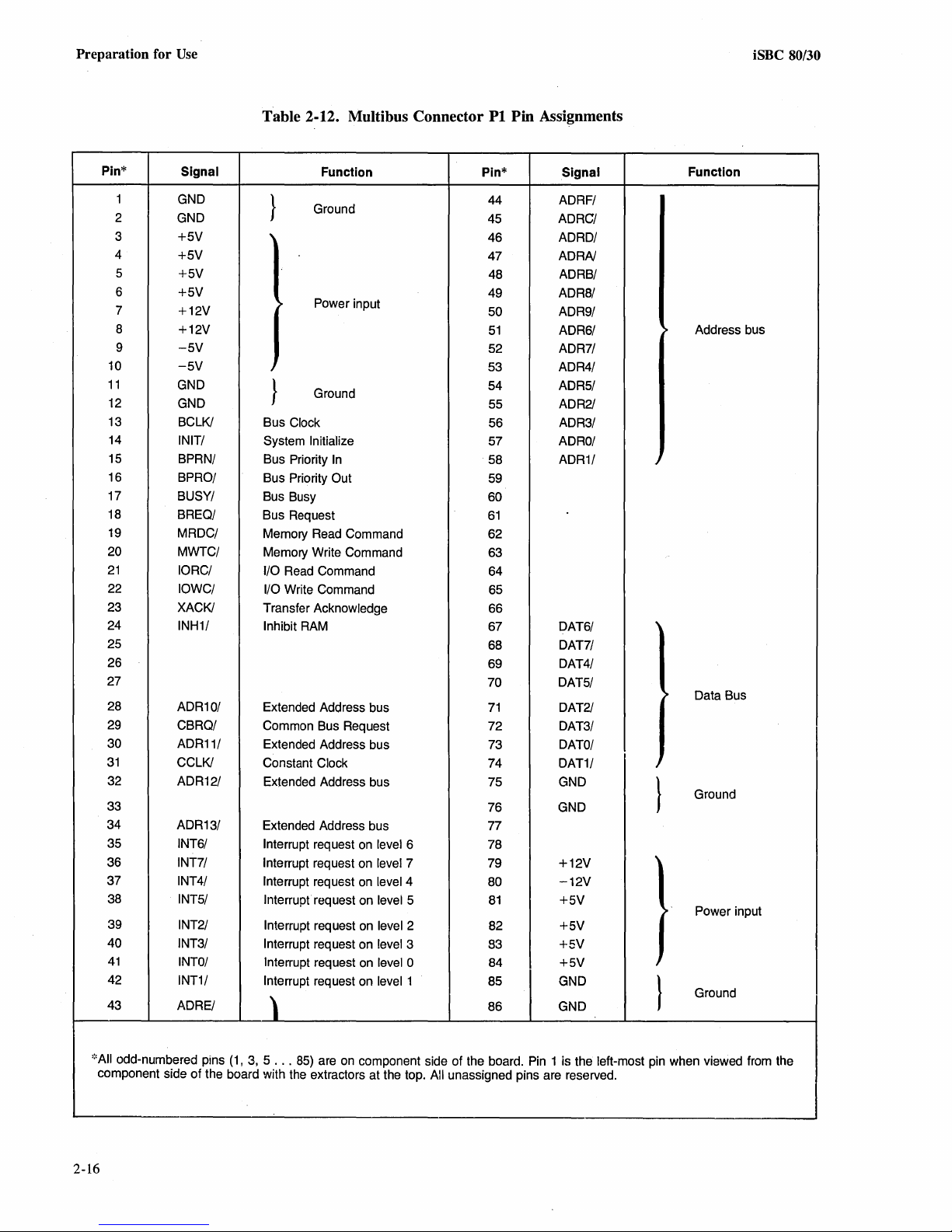
Preparation for
Use
iSBC 80/30
Pin*
1
2
3
4
5
6
7
8
9
10
11
12
13
14
15
16
17
18
19
20
21
22
23
24
25
26
27
28
29
30
31
32
33
34
35
36
37
38
39
40
41
42
43
Signal
GND
GND
+5V
+5V
+5V
+5V
+12V
+12V
-5V
-5V
GND
GND
BCLKI
INIT/
BPRN/
BPRO/
BUSY/
BREQ/
MRDC/
MWTC/
10RC/
10WC/
XACKI
INH1/
ADR10/
CBRQ/
ADR11/
CCLKI
ADR12/
ADR13/
INT6/
INT7/
INT4/
INT5/
INT2/
INT3/
INTO/
INT1/
ADRE/
Table 2-12. Multibus Connector
Function
Ground
}
,
Power input
>
J 53 ADR4/
Ground
}
Clock
Bus
System Initialize
Bus Priority
Bus Priority Out
Bus Busy
Bus Request
Memory Read Command
Memory Write Command
I/O
Read Command 64
I/O
Write Command 65
Transfer Acknowledge
Inhibit
Extended Address bus
Common Bus Request 72
Extended Address bus
Constant
Extended Address bus 75 GND
Extended Address bus
Interrupt
Interrupt
Interrupt
Interrupt
Interrupt
Interrupt
Interrupt request on level 0
Interrupt
In
RAM
Clock
request on level 6 78
request on level 7
request on level 4
request on level 5
request on level 2
request on level 3
request on level 1 85 GND
\
PI
Pin Assignments
Pin*
44
46 ADRD/
47
48
49
50 ADR9/
51
52
54 ADR5/
55 ADR2I
56 ADR3/
57
58 ADR1/
59
60
61
62
63
66
67 DAT6/
68 DAT7/
69 DAT4/
70
71
73
74
76 GND
77
79
80
81
82
83
84
86 GND
Signal
ADRF/
ADRC/ 45
ADRN
ADRB/
ADR8/
ADR6/
ADR7/
ADRO/
DAT5/
DAT2I
DAT3/
DATO/
DAT1/
+12V
-12V
+5V
+5V
+5V
+5V
Function
> Address bus
J
,
> Data Bus
J
Ground
I
,
>'
Power input
J
Ground
I
'::AII
odd-numbered pins
component side of the board with the extractors at the top.
2-16
(1,
3, 5
...
85)
are on component side of the board. Pin 1 is the left-most pin when viewed from the
All unassigned pins are reserved.
Page 30
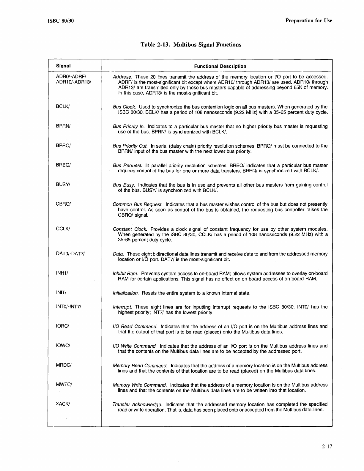
iSBC 80/30
Table 2-13. Multibus Signal Functions
Preparation for
Use
Signal
ADRO/-ADRF/
ADR10/-ADR13/
BClK!
BPRN/
BPRO/
BREQ/
BUSY/
CBRQ/
CClK!
Functional Description
Address. These 20 lines transmit the address of the memory location or I/O port to
ADRF/ is the most-significant bit except where
ADR13/ are transmitted
In
this case, ADR13/
Bus Clock. Used
iSBC 80/30,
Bus Priority
use of the bus. BPRN/ is synchronized with
Bus Priority
BPRN/ input of the bus master with the next
Bus Request.
requires
Bus Busy. Indicates that the bus
of the bus. BUSY/ is synchronized with
Common Bus Request. Indicates that a bus master wishes control of the bus but does not presently
have control. As soon as control of the bus
CBROI
Constant Clock. Provides a clock signal of constant frequency for use by other system modules.
When generated by the iSBC 80/30,
35-65 percent duty
to
BClK!
In.
Indicates to a particular bus master that no higher priority bus master
Out.
In
In
parallel priority resolution schemes, BREQ/ indicates that a particular bus master
control of the bus 'for one
signal.
only by those bus masters capable of addressing beyond 65K of memory.
is
the most-significant bit.
synchronize the bus contention logic on all bus masters. When generated by the
has a period
serial (daisy chain) priority resolution schemes, BPRO/ must be connected to the
cycle.
of
108 nanoseconds (9.22 MHz) with a 35-65 percent duty cycle.
or
more data transfers. BREQ/
is
in
use and prevents all other bus masters from gaining control
CClK!
ADR10/ through ADR13/ are used. ADR10/ through
BelK!.
lower bus priority.
is
synchronized with
BClK!.
is
obtained, the requesting bus controller raises the
has a period of 108 nanoseconds (9.22 MHz) with a
be
accessed.
is
requesting
BClK!.
DATO/-DAT7/
INH1/
INIT/
INTO/-INT7/
10RC/
10WC/
MRDC/
MWTC/
XACK!
Data. These eight bidirectional data lines transmit and receive data to and from the addressed memory
location or I/O port. DAT7/
Inhibit Ram. Prevents system access to on-board RAM;
RAM for certain applications. This
Initialization. Resets the entire system
Interrupt. These eight
highest priority;
I/O Read Command. Indicates that the address of
that the output of that port is
I/O
Write Command. Indicates that the address of
that the contents on the
Memory Read Command.
lines and that the contents of that location are to
Memory Write Command. Indicates that the address of a memory location
lines and that the contents on the Multibus data lines are to be written into that location.
Transfer Acknowledge. Indicates that the addressed memory location has completed the specified
or
write operation. That is, data has been placed onto or accepted from the Multibus data lines.
read
INT7/ has the lowest priority.
is
the most-significant bit.
signal has no effect on on-board access of on-board RAM.
to
a known internal state.
lines are for inputting interrupt requests to the iSBC 80/30.
to
be
read (placed) onto the Multibus data lines.
Multibus data lines are to be accepted by the addressed port.
Indicates that the address
allows system addresses to overlay on-board
an
I/O port is on the Multibus address lines and
an
I/O port
is
on the Multibus address lines and
of
a memory location is on the Multibus address
be
read (placed) on the Multibus data lines.
is
on the Multibus address
INTO/
has the
2-17
Page 31

Preparation for
Use
iSBC 80/30
Table 2-14. iSBC 80/30 DC Characteristics
Signals
ADRO/-ADRC/
ADRD/-ADRF
Symbol
VOL
VOH
VIL
VIH
IlL
IIH
ILH
ILL
*CL
VOL
VOH
VIL
VIH
IlL
IIH
*CL
Parameter
Description
Output Low Voltage
Output High Voltage
Input
Low Voltage
Input High Voltage
Current at Low V
Input
Input Current at High V
Output Leakage High Vo = 5.25V
Output Leakage Low
Capacitive Load
Output Low Voltage
Output High Voltage
Input
Low Voltage
Input High Voltage
Input
Current at Low V
Input Current at High V
Capacitive Load
Conditions
IOL
= 50 rnA
IOH = -10
VIN
= 0.45V
VIN
= 5.25V
Vo
= 0.45V
IOL
= 50 rnA
IOH
= 10 rnA
VIN
= 0.45V
VIN
= 5.25V
Test
rnA
Min.
2.4
2.0
2.4
2.0
Max. Units
0.5
0.8
-0.25
80
200
200
18
0.5
0.8
-0.5
200
25
V
V
V
V
rnA
/LA
/LA
/LA
pF
V
V
V
V
rnA
/LA
pF
ADR1
BCLI<!
BPRN/
0/ -ADR13/
VIL
VIH
IlL
IIH
*CL
VOL
VOH
VIL
VIH
IlL
IIH
*CL
VIL
VIH
IlL
IIH
*CL
Low Voltage
Input
Input High Voltage
CLn'rent
Input
Input Current at High V
Capacitive Load
Output Low Voltage
Output High Voltage
Input
Input High Voltage
Input
Input Current at High V
Capacitive Load
Input
Input High Voltage
Input
Input Current at High V
Capacitive Load
at Low V
Low Voltage
Current at Low V
Low Voltage
Current at Low V
VIN
= 0.45V
VIN
= 5.25V
IOL
= 59.5 rnA
IOH
=
-3
VIN
= 0.45V
VIN
= 5.25V
VIN = O.4V
VIN
= 2.4V
rnA
2.0
2.7
2.0
2.0
0.85
-0.25
10
18
0.5
0.8
-0.5
100
15
0.8
-1.6
40
18
V
V
rnA
/LA
pF
V
V
V
V
rnA
/LA
pF
V
V
rnA
/LA
pF
*Capacitive
load values are approximations.
2-18
Page 32

iSBC 80/30 Preparation for
Use
Signals
BPRO/
BREQ/
BUSY/, CBRQ/,
INTROUT/
(OPEN COLLECTOR)
CCLKI
Table 2-14. iSBC 80/30
Symbol
VOL
VOH
ILH
ILL
*CL
VOL
VOH
VIL
VIH
*CL
VOL
*CL
VOL
Parameter
Description
Output Low Voltage
Output High Voltage
Output Leakage High
Output Leakage Low
Capacitive Load
Output Low Voltage
Output High Voltage
Input Low Voltage
Input High Voltage
Capacitive Load
Output Low Voltage
Capacitive Load
Output Low Voltage
DC
Characteristics (Continued)
Test
Conditions
3.2 rnA
IOL=
IOH = -400
Vo = 5.25V
Vo = 0.45V
IOL= 20 rnA
IOH = -400
Vo=
Vo=
IOL= 20 rnA
IOL= 60 rnA
p.A
p.A
5.25V 100
0.45V
Min.
2.4 V
2.4 V
Max. Units
0.45 V
100
-100
15 pF
0.45 V
-100
15
0.45
20
0.5
p.A
p.A
p.A
p.A
pF
V
pF
V
DATO/-DAT7/
INH1/
INIT/
(SYSTEM RESET)
VOH
*CL
VOL
VOH
VIL
VIH
IlL
ILH
ILL
*CL
VIL
VIH
IlL
IIH
*CL
VOL
VO
VIL
Output High Voltage
Capacitive Load
Output Low Voltage
Output High Voltage
Input Low Voltage
Input High Voltage
Input Current at Low V
Output Leakage High
Output Leakage Low
Capacitive Load
Input Low Voltage
Input High Voltage
Current at Low V
Input
Input Current at High V
Capacitive Load 18
Output Low Voltage
High Voltage
H
Output
Input Low Voltage 0.8 V
IOH
=
-3
rnA
IOL= 50 rnA
IOH = -10
VIN
Vo = 5.25V
Vo = 0.45V
VIN
VIN
IOL
OPEN COLLECTOR
rnA
= 0.45V
= 0.5V
= 2.7V
= 46 rnA
2.7
15 pF
0.6
2.4 V
0.95 V
2.0
-0.25
100
100
18 pF
0.8
2.0
-2.0
50
0.4
V
V
V
rnA
p.A
p.A
V
V
rnA
p.A
pF
V
*Capacitive load values are approximations.
2-19
Page 33
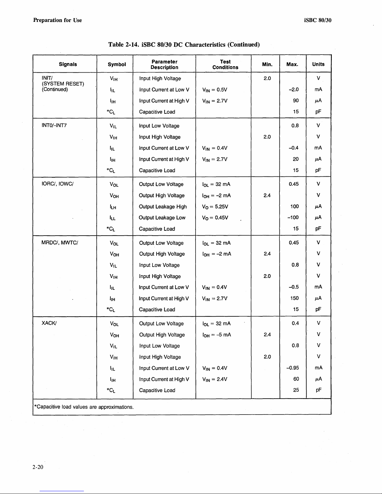
Preparation for
Use
iSBC 80/30
Table 2-14. iSBC 80/30 DC Characteristics (Continued)
Signals
INIT/
(SYSTEM RESET)
(Continued)
INTO/-INT7
IORC/, IOWC/
MRDC/, MWTC/
Symbol
VIW
IlL
IIH
*CL
VIL
VIH
IlL
IIH
*CL
VOL
VOH
ILH
ILL
*CL
VOL
VOH
VIL
VIH
IlL
IIH
*CL
Parameter
Description Conditions
High Voltage
Input
Input Current at Low V
Input Currerit at High V
Capacitive Load
Input Low Voltage
Input High Voltage
Input Current at Low V
Input Current at High V
Capacitive Load
Output Low Voltage
Output High Voltage
Output Leakage High
Output Leakage Low
Capacitive Load
Output Low Voltage
Output High Voltage
Input Low Voltage
Input High Voltage
Input
Current
at
Low V
Input Current at High V
Capacitive Load
VIN
VIN
VIN = O.4V
VIN
IOL
= 32 rnA
IOH = -2
Vo=
Vo=
IOL
IOH = -2
VIN
VIN
Test
= 0.5V
= 2.7V
= 2.7V
rnA
5.25V
0.45V
= 32 rnA
rnA
= 0.4V
= 2.7V
Min. Max.
2.0
-2.0
90
15
0.8 V
2.0
-0.4
20
15
0.45
2.4
100
-100
15
0.45
2.4
0.8
2.0
-0.5
150
15
Units
V
mA
/-LA
pF
V
mA
/-LA
pF
V
V
/-LA
/-LA
pF
V
V
V
V
rnA
/-LA
pF
XACK/
*Capacitive load values are approximations.
VOL
VOH
VIL
VIH
IlL
IIH
*CL
2-20
Output Low Voltage
Output High Voltage
Low Voltage
Input
Input High Voltage
Current at Low V
Input
Input Current at High V
Capacitive Load
IOL
= 32 mA
IOH = -5
VIN = O.4V
VIN
mA
= 2.4V
2.4
2.0
0.4
0.8
-0.95
60
25
V
V
V
V
rnA
/-LA
pF
Page 34

iSBC 80/30
Preparation for
Use
Parameter
tAS
tAH
tos
tOHW
.tCY
tCMoR
tCMOW
tCSWR
tCSRR
tcsww
tCSRW
tXACK1
tXACK2
tSAM
tACKRO
tACKWT
tOHR
tOXL
tXKH
tsw
tss
toSY
tNOO
tsCY
tsw
tlNIT
Table 2-15. iSBC 80/30
Overall
Max. Min.
Min.
(ns)
(ns)
50
50
50
50 50
358
365
Read
Max. Min.
(ns)
(ns) (ns) (ns)
50
50
50
Write
Max.
50
50
AC
Characteristics (Master Mode)
Description
Address setup time to command
Address hold time from command
Data setup to command
Data hold time from command
CPU cycle time
670 Read command width
575
390
Write command width
Read-to-write command separation
465 Read-to-read command separation
575
465
-195
-509
Write-to-write command separation
Write-to-read command separation
Read command to XACK 1 st sample point
Write command to XACK 1 st sample point
350 375 Time between XACK samples
75
0
-75
0 0 0
35
23
55
30
108 109
74
35
175
AACK to valid read data
AACK to write command inactive
Read data hold time
Read data setup to XACK
XACK hold time
Bus clock low
BPRN to BCLK setup time
BCLK to BUSY delay
BPRN to BPRO delay
Bus clock period (BCLK)
Bus clock low or high interval
or
high interval
3000 Initialization width
Remarks
1 wait state
With
1 wait state
With
In override mode
In
override mode
In override mode
In override mode
In override mode
In
override mode
In
override mode
When AACK is
When AACK is used
Supplied by system
From
iSBC 80/30 when terminated
From
iSBC 80/30 when terminated
After all voltages have stabilized
used
Table 2-16. iSBC 80/30 AC Characteristics (Slave Mode)
Parameter
tAS
tos
tOS1
tACK
tCMo
tAH
tOHW
tOHR
tXTH
*tACC
tlH
tlPW
*tCY
toS2
tRO
toxL
tsEP
tiS
*When an asynchronous refresh cycle occurs,
also added.
Minimum
(ns) (ns)
50
-200
480
720 Command width
0
0
0
0
50
100 Inhibit pulse width
680 920
535
25
200
-50
Maximum
1500
720
45
645
1865
555
Description
Address setup to command
Write data setup to' command
On-board memory cycle delay
Command to XACK
Address hold time
Write data hold time
Read data hold time
Acknowledge hold time
Access time to read data
Inhibit time from command trailing edge
Minimum cycle time
On board memory cycle delay
Refresh delay time
Read data setup to XACK
Command separation
Inhibit setup to command
tRO
is added to these parameters; when on-board memory cycle occurs,
From address to command
No refresh
Acknowledge turnoff delay
Blocks AACK if
tCY
Refresh delaying
Blocks RAM cycle and
Remarks
=.
tACK + tSEP
tiS>
SACK
tiS min.
tACK
tOS1
is
2-21
Page 35

iSBC 80/30
BCLKJ
BREa/
BPRN/
BUSY/
BPRO/
ADDRESS
WRITE
DATA
BCy
t
--1
~
tBW--1
'--
_________________
tDBO
~
______
IAS.IDS-_j"
I --j
H r-
STABLE ADDRESS
STA_BLE_DA_TA
tBW
____
...1
L
___
~X
~IAH.
(
IDHW
_
611-4
WRITE COMMAND/
WRT AACK/
READ COMMAND/
READ DATA
READ
XACKJ
~~~----------------------tCMDW------------------------------~~~V
\
. I
_____________________________
~------------tCMDR------------.~
T_A_C_KW_T_~
I~
~
~tACKRD
9
Figure 2-3. Bus Exchange Timing (Master Mode)
__
~
~~-----------
\-j~IXKH
b,XKO
I
J
2-22
Page 36

iSBC 80/30
ADDRESS
MWTCI
XACKJ
DATA
Preparation
~-------tCMD---"":""----~
..------tACK------+-I
for Use
I
r-----+---------------------------+-----+---~~
tDS
I
------~)(r~------------------DA-T-A-V-A-Ll-D-------------------
DUAL
PORT
RAM
WRITE
ADDRESS
MRDCI
XACKI
DATA DATA VALID
INH11
______
-J)(~
____________________________________________
!.------tACC------1~
1
Figure 2-4. Bus Exchange Timing (Slave Mode)
lIS
\
....
41-----------tIPW-----------1
DUAL PORT
2-26. SERIAL PRIORITY RESOLUTION
In a multiple bus master system, bus contention can be
resolved in an
cage by implementing a serial priority resolution scheme
as
shown in figure 2-5. Due
the
BPRO/ signal path, this· scheme is limited to a
maximum
controlling the Multibus.
figure 2-5, the bus master installed in slot J2 has the
highest priority and
iSBC 604 Modular Backplane and Card-
to
the propagation delay of
of
three bus masters capable
In
the configuration shown in
is
able
to
of
acquiring and
acquire control
of
the
~
IIH+
..
~1
RAM
READ
Multibus at any time because its BPRN/input
enabled (tied to ground) through jumpers
backplane.
If
the bus master in slot J2 desires control
it drives its
input
using the Multibus, the J2 bus master pulls its
output low and gives the
take control
(See figure 5-3.)
of
BPRO/ output high and inhibits the BPRN/
to
all lower-priority bus masters. When finished
13
bus master the opportunity to
of
the Multibus. If the
13
bus master does not
is
always
Band
N on the
the Multibus,
BPRO/
2-23
Page 37

Preparation for
Use
iSBC 80/30
15
~
BO
Nl
-
HIGHEST
PRIORITY
MASTER
J2
BPRNI
BPROI
16
P-
~
~
CO
Ml
-
15
BPRNI
J3
BPROI
16
~
1-.........4
EO
1
r--O
-
LOWEST
PRIORITY
MASTER
15
BPRNI
J4
BPROI
BPRO/AN
NOT
MASTERS.
USED
D BPRNI
BY
NON-
~6\
HO
iSBC
BACKPLANE
(BOTTOM)
1
-
PINS
604
484-2 Figure 2-5. Serial Priority. Resolution Scheme
desire to control the Multibus at this time, it pulls its
BPRO/ output low and gives the lowest priority bus
of
master in slot J4 the opportunity to assume control
Multibus.
The serial priority scheme can be implemented in a
designed system bus
signals are wired
if
the chaining of BPRO/ and BPRN/
as
shown in figure 5-3.
the
user-
2-27. PARALLEL PRIORITY RESOLUTION
A parallel priority resolution scheme allows up to
. masters to acquire and control the Multibus. Figure 2-6
illustrates one method
resolving bus contention in a system containing eight bus
masters installed in an
highest and two lowest priority bus masters are shown
installed in the
In the scheme shown in figure 2-6. the priority encoder
a Texas Instruments 74148 and the priority decoder is an
Intel 8205.
Input connections to the priority encoder
of
implementing such a scheme for
iSBC 604/614. Notice that the two
iSBC 604.
16
bus
determine the bus priority, with input 7 having the highest
priority and input
J3
bus master has the highest priority and the J5 bus
master has the lowest priority.
IMPORTANT: In a parallel priority resolution scheme,
BPRO/ output must be disabled on all
the
the iSBC 80/30, disable the BPRO/ output signal by
removi~g
removed on the other bus masters, either clip the
that supplies. the
cut the signal trace.
jumper 169-170.
BPRO/ output signal to the Multibus
2-28. ·POWER FAIUMEMORV PROTECT
CONFIGURATION
A mating connector must be installed in the iSBC 604/604
is
Modular Cardcage and Backplane to accommodate auxiliary connector P2. (Refer to figure 1-1.) Table 2-2 lists
0 having the lowest priority. Here, the
b~s
masters. On
If
a similar jumper cannot be
Ie
pin
or
2-24
Page 38

iSBC 80/30
Preparation for
Use
I
I
I
L
NOTE:
~
-I-
C)B
-I-
REFER
DISABLING
NO.2
PRIORITY
J2
BPRN/
(NOTE)
BREC/ p.!L
- - - - -
- - - - -
TO
TEXT
REGARDING
OF
BPRO/
NO.1
PRIORITY
(HIGHEST)
J3
~
BPRN/
(NOTE)
BREC/~
~
t---
- - - - -
AO
OC
~
t---
- - - -
--07
L-------0I6
BREC/INPUTS
f~g~CM~~TERS
THE
OUTPUT.
--0
{--o:
-.J'I
--
.--0
--0
r---t---oIIO
~
-r
- - - - - - - - - - -
'DC)
)E
-I-
-I-
- - - - - -
BUS
PRIORITY
RESOLVER
P P
R R
b b
R R
~
~
E E
R R
~:
E
C
3 E D 3
2
1 g g
NO.7
PRIORITY
J4
BPRN/
(NOTE)
BREC/
o-!L
70--
610-----'
0--
o--}g~~~GTS
0--
TO
MASTERS
IN
iSBC
2~
11:r-....--------f-4--.J
01:1.........-----+---1
614
F(
~
()H
t---
NO.8
PRIORITY
(LOWEST)
J5
BPRN/
(NOTE)
BREC/
- - - -
0-2!-
--
-,
iSBC604
G( I (BOnOM)
--
BACKPLANE
- J
484·1
Figure 2-6. Parallel Priority Resolution Scheme
some 60-pin connectors that can be used for this purpose;
flat crimp, solder, and wire wrap connector types are
listed. Table 2-17 correlates the signals and pin numbers
on the connector.
Procure' the appropriate mating connector for P2 and se-
it
in place
cure
a. Position holes
holes that are
as
follows:
in
P2 mating connector over mounting
in
line with corresponding
PI
mating
connector. .
b. From top
of
connector, insert two 0.5-inch
#4-40
pan head screws down through connector and mounting holes.
c. Install a flat washer, lock washer, and star-type nut on
each screw; then tighten the nuts.
When the mating connector for
power fail signals
as
listed in table 2-17. (The dc characteristics
to
the appropriate pins
P2
is
in place, wire the
of
the connector
of
the'
auxiliary signals are given in table 2-18.) In a typical
as
system, these signals would be wired
follows:
a. Connect auxiliary signal common and returns for
+5V,
-5V,
and + 12V backup batteries to P2 pins
1 and 2.
b. Connect +
-5V
battery input
battery input to
5V battery input
to
P2 pins 7 and
P2 pins
to
P2 pins 3 and 4;
8;
and + 12V
11
and 12. Remove jumpers
W7, W8, and W9.
c. Connect
PFS/input to P2 pin
17
and MEM PROT/
input to P2 pin 20.
d. Connect
PA/
input
to
P2 pin
19;
this signal
is
inverted and applied to the priority interrupt matrix.
To assign the
interrupt
PAl
irtput
as
the highest priority
(8085A TRAP), remove jumper
i37-i45
and connect jumper 134-137.
e. Connect HLT/ output at
indicator, which
P2 pin
28
to
external HALT
is
typically a light-emitting diode
(LED) mounted on the system enclosure.
f. Connect BTMO output at P2 pin 34 to external
TIME
OUT indicator, which is typically a LED
mounted on the system enclosure.
g. Connect
is
AUX RESET/ input to P2 pin 38. This signal
usually supplied
by
a momentary closure switch
mounted on the system enclosure.
h. Connect W AIT/ output at P2 pin 32 to external WAIT
indicator, which
is
typically a LED mounted on the
system enclosure.
2-25
Page 39

Preparation for
Use
_ _ _
__
T_able
2-17. Auxiliary
~onnect0l'
P2 Pin Assign"!ents
iSBC 80/30
Pin*
11
12
17
19
20
2S
~
32
34
3S
Signal
1
2
3
4
7
S
GND
GND
+5VAUX
+5VAUX
-5VAUX
-5V
AUX
+12V
+12
AUX
PFS/
PFI/
MEM PROT/
HLT/
WAIT!
BTMO
AUX
RESET/
AUX
- -
} Auxiliary
common
,
> Auxiliary backup battery supply
I
Power Fail Status. This externally supplied signal
SOS5A
microprocessor to allow the program to check the current status of the system power fail circuit. The status
instruction.
Power Fail
matrix. This signal should normally be jumpered to the
TRAP input.
Memory Protect. This externally supplied signal prevents access to RAM during battery
backup operation.
Halt. This output
Wait. This output
the
Bus Time
either halted or is hung up
in response to the previous
Auxiliary Reset. This externally supplied signal initiates a pseudo
i.e., initializes the board and resets the entire system to a known internal state.
Interrupt., This externally supplied signal
sign~1
indicates that the
SOS5A
Signal, which is the same as the
microprocessor
Out. This output signal indicates that the
is
Definition
is
applied to the SID input of the
is
checked by periodically executing a RIM
is
applied to the priority interrupt
SOS5A
microprocessor is halted.
CPU
either halted or in a wait state.
in
a wait state (Le., waiting for
I/O or Memory Command).
ALE
SOS5A
SOS5A
microprocessor
Signal, indicates that
microprocessor has
an
acknowledge signal
power~up
sequence;
*AII odd-numbered pins (1,
component side of the board with the extractors at the top .
3, 5 ...
59) are
on
component side of the board. Pin 1 is the left-most pin when viewed from the
. Table 2-18. Auxiliary Signal (Connector P2) DC Characteristics
Signals
PFS/, MEM PROT/
AUX RESET/
WAIT/
PFI/
Symbol
VIL
V
IH
IlL
IIH
CL
VIL
VIH
IlL
IIH
CL
VOL
VOH
CL
VIL
VIH
IlL
IIH
CL
Parameter
Description
Input Low Voltage
Input High Voltage
Input Current at Low V
Input Current at High V
Capacitive Load
Input Low Voltage
Input High Voltage
Current at Low V
Input
Input Current at High V
Capacitive Load
Output Low Voltage
Output High Voltage
Capacitive Load
Input Low Voltage
Input High Voltage
Current at Low V
Input
Input Current at High V
Capacitive Load
Test
Conditions
VIN=
O.4V
VIN= 2.4V
VIN
= 0.45V
VIN
= 5.25V
10L
= 17 rnA
IOH = -950
VIN
= 0.40V
VIN
= 2.7V
/LA
Min.
2.4
2.6
2.7
2.0
Max.
O.S
50
10
O.S
-0.25
10
10
0.5
15
O.SO
-0.4
20
15
Units
V
V
2
rnA
/L
pF
V
V
rnA
/LA
/L
V
V
pF
V
V
rnA
/LA
pF
F
2-26
Page 40

iSBC 80/30
Preparation for
Use
2-29. PARALLEL
I/O
CABLING
Parallel I/O ports E8, E9, and EA are controlled by the
Intel 8255A Programmable Peripheral Interface
1.
interfaced via edge connector J
are controlled by the optional Intel
Parallel I/O ports 1 and 2
8041/8741 Universal
Peripheral Interface and interfaced via edge connector
(Refer to figure 1-1.) Pin assignments for J 1
listed in tables 2-19 and
of
teristics
the parallel I/O signals are given in table 2-21.
2-20, respectively; dc charac-
(PPI) and
and·
J2 are
J2~
Table 2-2 lists some 50-pin edge connectors that can be
11
used for interface to
and J2; flat crimp, solder, and
wirewrap connector types are listed.
transmIssion path from the I/O source
The
to
the iSBC
80/30 should be limited to 3 meters (10 feet) maximum.
The. following bulk cable types (or equivalent) are recommended for interfacing with the parallel
3M
a. Cable, flat, 50-conductor,
3306-50.
b. Cable, flat, 50-conductor (with ground plane),
I/O ports:
3M
3380-50.
c. Cable, woven, 25-pair,
An Intel iSBC 956 Cable Set, consisting
3M
3321-25.
of
two cable
assemblies, is recommended for parallel I/O interfacing.
Table 2-19. Connector
Pin* Function
1 Ground
3
5
7
9
11
13
15
17
19
21
23
25 26
27
29
31
33
35
37
39
41
43
45
47 Ground
49
*AII odd-numbered pins
ponent. side of the board.
viewed form the component side of the board with
when
the extractors at the top.
I
Ground
Ground
I
Ground
Gror
Ground
Jl
Pin Assignments
Pin*
2 Port
4
6
8
10
12
14 Port
16
18
20
22
24
28
30
32
34
36
38
40
42
44
46
48
50
(1,
3,
5,
...
Pin
49) are
1 is the right-most pin
Port
Port
Port
Port
Port
Port
Port
Port
Port
Port
Port
port
Port
Port
Port
Port
Port
Port
Port
Port
Port
Port
EXT
Function
E9
bit 7
E9
bit 6
E9
bit 5
E9
bit 4
E9
bit 3
E9
bit 2
E9
bit 1
E9
bit 0
EA
bit 3
EA
bit 2
EA
bit 1
EA
bit 0
EA
bit 4
EA
bit 5
EA
bit 6
EA
bit 7
E8
bit 7
E8
bit 6
E8
bit 5
E8
bit 4
E8
bit 3
E8
bit 2
E8
bit 1
E8
bit 0
INTRO/
on
com-
Both cable ,:!ssemblies consist
with a
50-pin PC connector at one end. When attaching
11
or
the cable to
J2, be sure that the connector is oriented
of
a 50-conductor flat cable
properly with respect to pin 1 on the edge connector.
(Refer to the footnotes in tables 2-19 and
2-30. SERIAL
I/O
CABLING
2~20.)
Pin assignments and signal definitions for RS232C serial
I/O interface are listed in table 2-10. An Intel iSBC 955
Cable Set is recommended for RS232C interfacing.
cable assembly consists
a 26-pin
PC connector at one end and an RS232C inter-
of
a 25 -conductor flat cable with
One
face connector at the other end. The second cable assembly includes an RS232C connector at one end and has
spade lugs at the other end; the spade lugs are used to
interface to a teletypewriter.
(Se·e Appendix B
for
ASR-33 TTY interface instructions.)
For
OEM applications where cables will be made for the
80/30, it is important to note that the mating connec-
iSBC
13
tor for
. has 26
25 pins. Consequently, when connecting the 26-pin-
piJ?~
.whereas the RS232C connector has
mai--
ing connector to 25-conductor flat cable, be sure that the
Table 2-20. Connector
Pin* Function Pin*
1
3
5 6
7
9
11
13
15
17
19
21
23
25
27
29
31
33
35
37
39
41
43
45
47
49
*AII odd-numbered pins
ponent side of the board.
when viewed from
the
* *Jumpered pin or function. Refer to figure 5-2 sheet
Ground 2
I
Ground
Ground
I
Ground 32
Ground 34 Port 1 bit 7
' I
Ground 48 Port 1 bit
Ground
extractors at the top.
the component side of the board with
J2
Pin Assignments
Port 2 bit 7
Port 2 bit 6
4
Port 2 bit 5
Port 2 bit
8
10 Port 2 bit
12
14
16
18
20
22
24 Not Used
·26
28
30
36
38
40 Port 1 bit 4
42
44
46
50
(1,
3,
Pin
Port 2 bit 2* *
Port 2 bit 1* *
Port 2 bit 0* *
TO
T1
Not Used
Not Used
Not Used
41
41
Port 1 bit 6
Port 1 bit 5
Port 1 bit 3
Port 1 bit 2
Port 1 bit 1
EXT INTR1/
5,
...
49) are
1 is the right-most pin
Function
4*
*
3*
*
Input
Input
RS232 Out* *
RS232 In* *
0
on
com-
5.
Page 41

Preparation for
Use
table
2·21. Parallel
1/0
Signal (Connectors
JlIJ2)
DC Characteristics
iSBC
80/30
Signals
Port E8
Bi
di
rectional
Drivers
8255A
Driver/Receiver
8041/8741 A
Driver/Receiver
Symbol
VOL
VOH
VIL
VIH
IlL
CL
VOL
VOH
VIL
VIH
IlL
IIH
CL
VOL
VOH
VIL
VIH
IlL
IIH
CL
Parameter
Description
Output Low Voltage
Output High Voltage
Input
Low Voltage
Input High Voltage
Input
Current at Low V
Capacitive Load 18
Output Low Voltage
Output High Voltage
Input
Low Voltage
Input High Voltage
Current at
Input
Input Current at High V
Capacitive Load
Output Low Voltage
Output High Voltage
Low Voltage
Input
Input High Voltage
Input
Curr~nt
Input Current at High V
Capacitive Load
LowV
at Low V
Test
Conditions
IOL = 20
IOH = -12
VIN
IOL
IOH = -200
VIN
VIN
IOL
IOH
VIN
VIN
rnA
= 0.45V
= 1.7 rnA
= 0.45
= 5.0
= 1.6 rnA
='50
= 0.8V
= 5.25V
rnA
JLA
JLA
Min.
2.4
2.0
2.4
2.0
2.4
2.0
Max.
0.45
0.95 V
-5.25
0.45
0.8
10
10
18
0.45
0.8
0.4
10
18
Units
V
V
V
rnA
pF
V
V
V
V
JLA
JLA
pF
V
V
V
V
JLA
JLA
pF
EXT
EXT
INTO
INTi
VIL
VIH
IlL
IIH
CL
VIL
VIH
IlL
IIH
CL
2-28
Low Voltage
Input
Input High Voltage
Current at Low V
Input
Input Current at
Capacitive
Low Voaltage
Input
Input High Voltage
Current at Low V
Input
Input Current at High V
Capacitive Load
HighV
~oad
VIN
= 0.4V
VIN
= 2."N
VIN = O.4V
VIN
= 2."N
2.0
2.0
0.8
-5.5
20
15
0.8
-0.4
20
15
3mA
3
JLA
rnA
JLA
V
V
pF
V
V
pF
Page 42

iSBC 80/30
Preparation for
Use
cable makes contact with pins 1 and 2
of
the mating
connector and not with pin 26. Table 2-22 provides pin
correspondence between connector
connector. When attaching the cable
13
and
an
RS232C
to
J3, be sure that the
PC connector is oriented properly with respect to pin 1 on
the edge connector. (Refer to the footnote in table
Table 2-22. Connector
--
PC
Conn.
J3
1
2
3
4 2 17
5
6
7
8 4
9
10
11
12
13
Pin Correspondence
RS232C
Conn. J3
14
1
15
16
3
17
18
5
19
6
20
PC
J3
Vs
Conn.
14
15
16
18
19
20
21
22
23
24
25
26
RS232C
2-10.)
RS232C
Conn.
7
21
8
22
9
23
10
24
11
25
12
N/C
13
2-31. BOARD INSTALLATION
Always turn off the computer system power
supply before installing
80/30
board and before installing
device interface cables. Failure
precautions, can result in damage to the board.
In an iSBC 80 Single Board Computer based system,
install the
iSBC 80/30 in any slot that has not been wired
for a dedicated function. In an Intellec System, install the
iSBC 80/30 in any slot except slot 1 or 2. Make sure that
auxiliary connector
P2 (if used) mates with the userinstalled mating connector. Attach the appropriate cable
assemblies to connectors J 1 through 13.
or
removing the iSBC
or
removing
to
take these
2-29/2-30
Page 43

PROGRAMMING INFORMATION
3-1. INTRODUCTION
This chapter lists the on-board memory and I/O address
assignments, describes the effects
command, and provides programming information for the
following programmable chips:
a. Intel
8251A
USART
Asynchronous Receiver/Transmitter) that controls
the serial
b. Intel 8253
I/O port.
PIT (Programmable Interval Timer) that
controls various frequency and timing functions.
c. Intel
8255A PPI (Programmable Peripheral Inter-
face) that controls the three parallel
d.
Intel 8259A PIC (Programmable Interrupt Controller) that can handle up
interrupts for the on-board 8085A microproces·sor
(CPU).
e. Intel 8041/8741 UPI (Universal Peripheral Inter-
face).
This
chapt~r
also discusses the Intel 8085A Microprocessor interrupt capability. The instruction set for the
is
included in Appendix
A;
programming with Intel's assembly language
8080/8085' Assembly Language Programming Man-
the
Order No. 9800310.
ual,
of
a system initialize
(Universal
Synchronous/
I/O ports.
to
eight vectored pfi:ority
8085A
a complete description
is
given in
of
CHAPTER 3
in
a wait state. In this situation, the only way to free the
CPU is to initialize the system
3-5.
3-3. MEMORY ADDRESSING
The iSBC 80/30 includes 16K
IC sockets to accommodate up to 8K
ROM/PROM. The iSBC 80/30 features a two-port RAM
access arrangement in which the on-board RAM can be
accessed by the on-board
or
by another bus master board via the Multibus. The
ROM/PROM can be accessed only
The on-board RAM can be accessed
ter that currently has control
noted, however, that even though another bus master may
be continuously accessing the
RAM, this does not lock out the
on-board RAM. In this situation, Memory Commands
from the
leaved. This,
the current access by the controlling bus master
pleted.
Addresses for
RAM are provided in table 3 -1. Note that the
PROM
CPU and the controlling bus master are inter-
of
course, will impose CPU wait states until
CPU access
address space depends on the user's configura-
as
described in paragraph
of
dynamic RAM and two
of
user-installed
8085A microprocessor (CPU)
by
the CPU.
by
another bus mas-
of
the Multibus. It should be
iSBC 80/30 on-board
CPU from accessing the
is
com-
of
ROM/PROM and on-board
ROM!
This chapter does not provide assembly language pro-
gramming information for the optional Intel
(Universal Peripheral Interface). This information
UPI
8041/8741
available in the UPI-41 User's Manual, Order No.
9800504A.
3-2. FAILSAFE TIMER
The 8085A microprocessor (CPU) expects an acknowl-
I/O
edge signal to be returned from the addressed
memory device in response to each Read
mand. The
triggered during T
iSBC 80/30 includes a Failsafe Timer that is
1
of
every machine cycle.
Timer is enabled by hardwire jumper
2-4, and an acknowledge signal"
is
or
Write Com-
If
the Failsafe
as
described in table
not received within
10 milliseconds, the Failsafe Timer will time out and
allow the
CPU to exit the wait state. As described in
Chapter 2, provision is made so that the Failsafe Timer
output
(BUS TIME OUT) can optionally be used to inter-
rupt the
If
signal
CPU and/or to drive a front panel indicator.
the Failsafe Timer is not enabled, and an acknowledge
is
not returned for any reason, the CPU will hang up
or
Table 3-1. On-Board Memory Addresses
(For
CPU Access)
is
On-Board
Memory Configuration
ROM/PROM One 1K x 8 chip
ROM/PROM
ROM/PROM One 4K x 8 chip
RAM
RAM
*Oefault (factory connected) jumper; refer to paragraph 2-16. Address-
ing RAM outside the jumper-selected
request via the
Two 1K x 8 chips
One
2K x 8 chip
Two 2K x 8 chips
Two
4K
x 8 chips
8K
Access 2000-3FFF
*16K
Access
Multibus.
Legal Address lllegal Address
0OOO-03FF
0OOO-07FF
0OOO-07FF
OOOO-OFFF
OOOO-OFFF
0OOO-1FFF
*4000-5FFF
6000-7FFF
8000-9FFF
AOOO-BFFF
COOO-OFFF
EOOO-FFFF
*4000-7FFF
8000-BFFF
COOO-FFFF
block results
0400-07FF
-
0800-0FFF
-
1000-1FFF
-
None
None
None
None
None
None
None
None
None
None
in
an
off-board
3-1
Page 44

Programming Information
iSBC 80/30
tion, and that the RAM address space depends on whether
the board jumpers are configured to allow the
access 8K or 16K
of
on-board RAM.
CPU to
For Multibus access, the on-board RAM may be mapped
into any 8K
straints
or
16K segment within the addressing con-
of
the controlling bus master. In other words, for
16-bit Multibus addressing, the RAM may be mapped
into any 8K or 16K segment
space. For
20-bit Multibus addressing, the RAM· may be
mapped into any 8K or 16K segment
of
the 64K byte address
of
the I-megabyte
address space. Additional information is provided in
paragraphs 2-17 through 2-19.
When the
PROM
Acknowledge (AACK/)
prevent imposing a
CPU is addressing on-board memory (ROM/
or
RAM), an internal PROM
is
automatically generated to
or
RAM Advanced
CPU wait state. When the CPU
is
addressing system memory via the Multibus, the CPU
must first gain control
or
Memory Read
Memory Write Command is given, must
of
the Multibus and, after the
wait for a Transfer Acknowledge (XACK/) to be received
from the addressed memory device. The Failsafe Timer,
if
enabled, will prevent a CPU hang-up in the event
memory device equipment failure
It should be noted in table 3
configur~
ROM/PROM such
or
a bus failure.
-1
that it
as
is
to create illegal ad-
of
possible to
dresses. If an illegal address is used in conjunction with a
Memory Write Command
AACK/ signal
legal and the
is
generated as though the address was
CPU will continue executing the program.
to
ROM/PROM, a PROM
However, in this case, erroneous data will be returned.
Table
3-2.
1/0
Address Assignments
1/0
Address
D80r
DA
D9
or
DB
DC
DD
DE
DF
E4
or
E6
a
E5
or
E7
E8
E9
EA
Chip
Select
8259A PIC
PIT
8253
8041/8741 A
UPI (J2)
8255A
PPI
Function
Write:
ICW1, OCW2, and OCW3
Read: Status
Write: ICW2
Read:
Write: CounterO (Load Count
Read: Counter
Write: Counter 1 (Load Count
Read: Counter 1
Write:Counter2
Read: Counter 2
Write:
Read: None
Write: Data
(J2)
Read: Data
Write: Command
Read: Status
Write: Port A (J1)
Read: Port A (J1)
Write: Port B (J1)
Read: Port B (J1)
Write: Port C (J1)
Read: Port C (J1)
and
and
OCW1 (Mask)
Control
OCW1
0
(Load Count + N)
Ports 1
are
8041/8741
software
)
instructions.
Poll
(Mask)
and
selected
+ N)
+ N)
2
by
•
3-4. I/O ADDRESSING
The on-board 8085A microprocessor (CPU) communicates with the programmable chips through a sequence
I/O Read and I/O Write Commands.
3 -2, each
imal
of
these chips recognizes four separate hexadec-
I/O addresses that are used
As
shown in table
to
control the various
of
programmable functions. Where two hexadecimal addresses are listed for a single function, either address may
be used. For example, an
will read the status
I/O Read Command
of
the 8251A USART.
to
ED
or
EF
NOTE
The on-board I/O functions are not accessible to
another bus master via the Multibus.
3-5. SYSTEM INITIALIZATION
When power is initially applied to the system, an Initialize
(INIT/) signal is automatically generated that clears the
internal Program Counter, Instruction Register, and Interrupt Enable flip-flop and
8255A PPI, and optional 8041/8741A UPI as follows:
'·'resets" the 8251A USART,
EB
or
EE
EC
or
EF
ED
a.
The 8251A USARTis setto an
for a set
8251A
USART
of
Command Words to program the desired
Write: Control
Read: None
Write: Data (J3)
Read: Data (J3)
Write: Mode
Read: Status
or
"idle"
Command
mode, waiting
function.
b. All three ports
the 8255A PPI are set
to
the input
of
mode.
c. The 8041/8741A
UPI internal Program Counter and
Status flip-flops are cleared.
The 8253 PIT and 8259A PIC are not affected by the
power-up sequence.
The INIT/ signal
remainder
is
also gated onto the Multibus to set the
of
the system components to a known internal
state.
3-2
Page 45

iSBC 80/30
The
!NIT/signal
can also be generated by an auxiliary
RESET switch. Pressing and releasing the RESET switch
as
produces the same effect
the INIT/ signal described
above.
3-6. 8251A USART PROGRAMMING
I scs I
ESD I EP I PEN I L21
LI
I
I 0 I 0 I
L_
Programming
CHARACTER LENGTH
1
0
0 0 1
5 6
81TS
BITS BITS
Information
1
0
1
8
1
BITS
The USART converts parallel output data into virtually
any serial output data format (including IBM Bi-Sync) for
or
half-
full-duplex operation. The USART also converts
serial input data into parallel data format.
Prior to starting transmitting or receiving data, the
USART must be loaded with a set
of
control words. These
control words, which define the complete functional op-
of
eration
(internal
instruction
the USAR T, must immediately follow a reset
or
external). The control words are either a Mode
or
a Command instruction.
3-7. MODE INSTRUCTION FORMAT
The Mode 'instruction word defines the general charac-
of
the
US
teristics
ART and must follow a re$et operation.
Once the Mode instruction word has been written into the
USART, sync characters
or
command instructions may be
inserted. The Mode instruction word defines the following:
a.
For Sync Mode:
(1) Character length
(2) Parity enable
(3) Even/odd parity generation and check
(4) External sync detect (not supported by
iSBC 80/30)
(5) Single
b.
For
(1) Baud rate factor
or
double character sync
Async Mode:
(Xl,
X16,
or
X64)
(2) Character length
(3) Parity enable
(4) Even/odd parity generation and check
(5) Number
of
stop bits
Instruction word and data transmission formats for syn-
chronous and asynchronous modes are shown in figures
3-1 through 3-4.
3-8. SYNC CHARACTERS
Sync characters are written to the USAR T in the syn-
US
chronous mode only. The
either one or two sync characters; the format
is
characters
at the option
ART can be programmed for
of
the sync
of
the programmer.
3-9. COMMAND INSTRUCTION FORMAT
The Command instruction word shown in figure 3-5 con-
of
trols the operation
the addressed USAR T. A Command
PARITY
ENABLE
(1
- ENABLEI
(0 - DISABLEI
EVEN
PARITY
l'
0-000
EXTERNAL
1 • SYNDET IS AN INPUT
0-
-
SINGLE CHARACTER SYNC
1 • SINGLE SYNC CHARACTER
O'
GENERATION/CHE
EVEN
SYNC DETECT
SY'IIDET IS AN OUTPUT
DOUBLE SYNC CHARACTER
Figure 3-1. USART Synchronous Mode
Instruction Word Format
CPU
BYTES (5-8 BITS/CHARI
II
DATA
CH:,RACTERS
RECEIVE FORMAT
SYNC
CHAR
ASSEMBLED SERIAL
SYNC I
1
CHAR
DATA
OUTPUT
(T.DI
DATA
CHA~,...AC_T_ER_S_---'
SERIAL
DATA
INPUT
(R.DI
~
CPU
BYTES (5-8 BITS/CHARI
DATA
CH~RACTERS
Figure 3-2. USART Synchronous Mode
I
S2 I SI I EP I PEN I L2j
Transmission
L 1 I
Format
B21
B,
I
BAUD RATE FACTOR
0 1
~
0 0 1
SYNC
MODE
CHARACTER LENGTH
0 1
0 0
5
BITS BITS
PARITY
~
ENABLE
1
EVEN
PARlfY
0
EVEN
1
NUMBER
0 1
0
INVALID
(ONl Y EFFECTS
REQUIRES
STOP
BIT)
(lXI
6 1
ENABLE
0
0
GENERATION/CHE
0-000
OF
STOP
0
1
BIT
MORE
0
(64XI
(16XI
0
1
8
BITS BITS
DISABLE
BITS
0
1
1'1}
BITS BITS
Tx;
Rx
NEVER
THAN
ONE
Figure 3-3. USART Asynchronous Mode
Instruction Word Format
CK
1
1
1
1
CK
1
1
2
3-3
Page 46
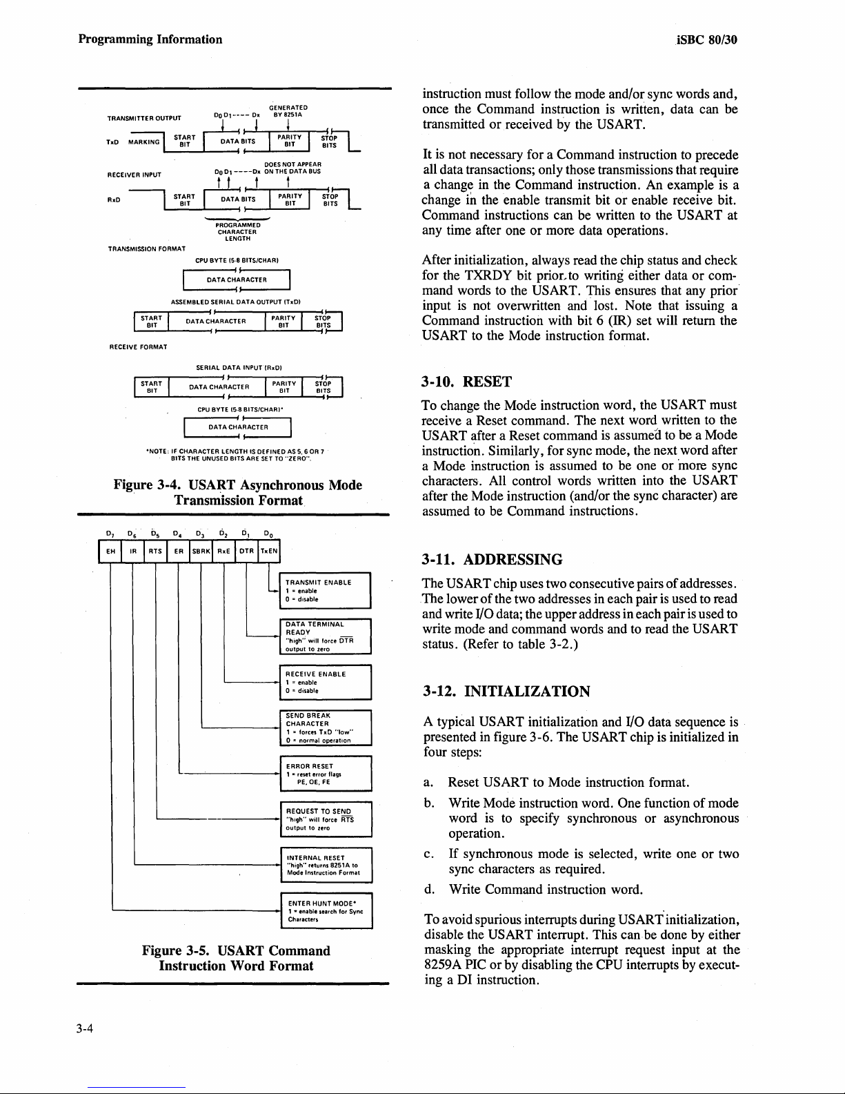
Programming Information
iSBC 80/30
instruction must follow the mode and/or sync words and,
Ox
----Ox
B\-IT_S
C:!,RACTER
DATA
OUTPUT
INPUTlRxDI
I-----L.--
','
,...A_CT_E_R
IS
GENERATED
BY
DOES
ON
THE
--'-
__
_ .....
DEFINED
SET
TO
8251A
NOT
DATA
(hOI
AS
"ZERO".
STJ;!
BITS
APPEAR
BUS
ST6;!
.....
Brrs
STO~
STOD
BITS
.........
---f
5, 6 OR
7
L
L
DO
01----
Do
RECEIVER INPUT
RxD I
TRANSMISSION FORMAT
RECEIVE FORMAT
STB~~T
ASSEMBLED SERIAL
L--_-'--_DA_T_A-iCHI-AR_AC_T_ER_-L--:;...----"L...-~BITW
'NOTE:
IF CHARACTER LENGTH
BITS THE UNUSED BITS ARE
01
t t t t
G
PROGRAMMED
CHARACTER
LENGTH
CPU
BYTE (5·8 BITS/CHARI
DATA
DATA
SERIAL
DATA
CHARACTER
CPU
BYTE (5·8 BITS/CHAR)'
L...-_D_AT_A_C~H:~
Figure 3-4. USART Asynchronous Mode
. Transmission Format
once the Command instruction is written, data can be
or
transmitted
received by the USART.
It is not necessary for a Command instruction to precede
all data transactions; only those transmissions that require
a change in the Command instruction. An example is a
change
in the enable transmit bit
Command instructions can be written to the
any time after one
or
more data operations.
After initialization, always read the chip status and check
for the TXRDY bit
mand words to the
input
is
not overwritten and lost. Note that issuing a
prior, to writing either data
USART. This ensures that any prior
Command instruction with bit 6 (IR) set will return the
USART to the Mode instruction format.
3-10. RESET
To change the Mode instruction word, the USART must
receive a Reset command. The next word written to the
USART after a Reset command is assumed to be a Mode
instruction. Similarly, for sync mode, the next word after
a Mode instruction is assumed to be one
characters. All control words written into the
after the Mode instruction (and/or the sync character) are
assumed to be Command instructions.
or
enable receive bit.
USAR T at
or
or
more sync
USART
com-
'-------i
'---
____
....
_---'-
____
----I
L-..
_________
L-..
__________
Figure 3-5. USART Command
Instruction Word Format
TRANSMIT
1 = enable
0=
disable
DATA
READY
"high"
output
RECEIVE
1 = enable
o • disable
SEND
-1
CHARACTER
1 = forces
o = normal operation
ERROR RESET
--1
1 z: reset error
PE,
REQUEST TO SEND
"high"
output
INTERNAL
-I
"high"
Mode
ENTER
--I
l'
Characters
TERMINAL
will
to
BREAK
OE,
will
to
returns
Instruction
HUNT
enable
ENABLE
lorce
zero
ENABLE
TxD
flags
FE
force RTS
zero
RESET
8251A to
MODE'
search
DTR
"low"
Format
for
Sync
3-11. ADDRESSING
The USAR T chip uses two consecutive pairs
of
.The lower
and write
the two addresses in each pair
VO
data; the upper address in each pair
write mode and command words and to read the
status. (Refer to table 3-2.)
of
addresses.
is
used to read
is
used to
USAR T
3-12. INITIALIZATION
A typical USART initialization and
presented in figure 3-6. The USART chip is initialized in
four steps:
a. Reset
USART to Mode instruction format.
b. Write Mode instruction word.
word is to specify synchronous or asynchronous
operation.
c.
If
synchronous mode
sync characters
d.
Write Command instruction word.
as
required.
is
To avoid spurious interrupts during
disable the
USART interrupt. This can be done by either
masking the appropriate interrupt request input at the
PIC
or
8259A
by disabling the CPU interrupts by execut-
ing a DI instruction.
VO
data sequence
One function
selected, write one
USART initialization,
of
mode
or
two
is
3-4
Page 47
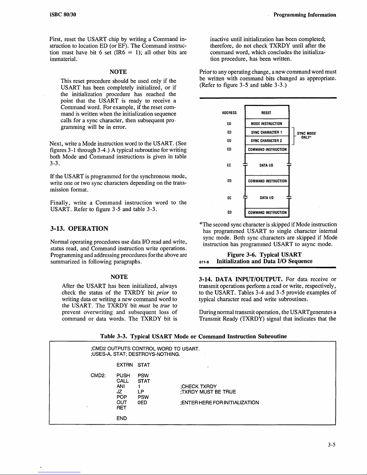
iSBC 80/30
Programming Information
First, reset the USART chip by writing a Command in-
struction to location ED (or EF). The Command instruction must have bit 6 set (lR6
= 1); all other bits are
immaterial.
NOTE
This reset procedure should be used only
USART has been completely initialized,
if
or
the
if
the initialization procedure has reached the
point that the
Command word. For example,
mand
is
calls for a sync character, then subsequent
USART
is
ready to receive a
if
the reset com-
written when the initialization sequence
pro-
gramming will be in error.
Next, write a Mode instruction word to the
figures 3
-1
through 3 -4.) A typical subroutine for writing
both Mode and Command instructions
USART. (See
is
given
in
table
3-3.
If
the USART
write one
is
programmed for the synchronous mode,
or
two sync characters depending on the trans-
mission format.
Finally, write a Command instruction word to the
USART. Refer to figure 3-5 and table 3-3.
inactive until initialization has been completed;
therefore, do not check TXRDY until after the
command word, which concludes the initialization procedure, has been written.
Prior
to
any operating change, a new command word must
be written with command bits changed as appropriate.
(Refer to figure 3-5 and table 3-3.)
ADDRESS
ED
ED
ED
ED
EC
ED
EC
ED
:~
.~
RESET
MODE
INSTRUCTION
SYNC
CHARACTER
SYNC
CHARACTER
COMMAND
DATA
COMMAND
DATA
COMMAND
1
2
INSTRUCTION
1/0
:~
::~
1/0
INSTRUCTION
INSTRUCTION
}
SYNC
ONLY·
MODE
3-13. OPERATION
Normal operating procedures use data I/O read and write,
status read, and Command instruction write operations.
Programming and addressing procedures for the above are
summarized in following paragraphs.
NOTE
After the USART has been initialized, always
of
check the status
writing data or writing a new command word to
the
USART. The TXRDY bit must be true to
prevent overwriting and subsequent loss
command
or
;CMD2 OUTPUTS CONTROL WORD TO USART.
;USES-A, STAT; DESTROYS-NOTHING.
CMD2:
the TXRDY bit prior to
of
data words. The TXRDY bit is
Table
3-3. Typical USART Mode
EXTRN
PUSH
CALL
ANI
JZ
POP
OUT
RET
STAT
PSW'
STAT
1
LP
PSW
OED
;CHECK TXRDY
;TXRDY
;ENTER HERE
*The second sync character
has programmed
USART to single character internal
is
skipped
if
Mode instruction
sync mode. Both sync characters are skipped
instruction has programmed
Figure
611·6 Initialization
3-14. DATA
3-6. Typical USART
and
INPUT/OUTPUT.
transmit operations perform a read
USART. Tables 3-4 and 3-5 provide examples
to the
USART to async mode.
Data
I/O
Sequence
For data receive
or
w.rite, respectively,
typical character read and write subroutines.
During normal transmit operation, the
USARTgenerates a
Transmit Ready (TXRDY) signal that indicates that the
or
Command
MUST
Instruction
BE
TRUE
FOR INITIALIZATION
Subroutine
if
Mode
or
of
END
3-5
Page 48

Programming Information
Table 3-4. Typical USART Data Character Read Subroutine
;RX1
READS DATA CHARACTER FROM USART.
;USES-STAT; DESTROYS-A,FLAGS.
EXTRN STAT
iSBC
80/30
RX1: CALL
ANI
JZ
IN
RET
END
STAT
2
RX1
OEC
;CHECK FOR RXRDY
;ENTER HERE
IF RXRDY IS TRUE
Table 3·5. Typical USART Data Character Write Subroutine
;TX1
WRITES DATA CHARACTER FROM REG A TO USART.
;USES-STAT; DESTROYS-A,FLAGS.
EXTRN STAT
TX1:
TX11:
PUSH
CALL
ANI
JZ
POP PSW
OUT
RET
END
PSW
STAT
1
TX11
OEC
;SAVE DATA
;CHECK
;ENTER HERE
FOR TXRDY
IFTXRDY IS TRUE
USART is ready to accept a data character for transmission. TXRDY is automatically reset when the
a character into the
USART.
CPU loads
Similarly, during normal receive operation, the USART
generates a Receive Ready (RXRDY) signal that indicates
that a character has been received and is ready for input to
the CPU. RXRDY is automatkally reset when a character
is read by the
The TXRDY and RXRDY outputs
CPU.
of
the USART are
available at the priority interrupt jumper matrix. If, for
instance, TXRDY and RXRDY are input to the 8259A
PIC, the PIC resolves the priority
af.l.d
drives the INTR
input high to the CPU. TXRDY and RXRDY are also
available in the status word. (Refer to paragraph 3-15.)
3·15. STATUS READ. The CPU can determine the
status
of
the serial Va port by issuing an
or
mand to the upper address (ED
of
The format
the status word is shown in figure 3 -7. A
EF)
typical status read subroutine is given in table 3 -6.
3-6
of
Va
the
Read Com-
US
ART chip.
3-16. 8253 PIT PROGRAMMING
A 22.1184 -MHz crystal oscillator supplies the basic clock
frequency for the programmable chips. This clock frequency is divided by 9, 18, and 144 to produce three
Jumper-selectable clocks: 2.4576 MHz, 1.2288 MHz,
Thes~
and 153.6 kHz.
0,
Counter
Counter 1, and Counter 2
default (factory connected) and optional jumpers for
selecting the clock inputs to the three counters are listed in
table 2-4.
Default jumpers connect the output
TXC and RXC inputs
included so that Counters
interrupts
or
provide an event clock to the 8041/8741 UPI
and a count out clock to 8255A
Before programming the 8253
clock frequency and the output function
three counters. These factors are determined and established by the user during the installation.
clocks are available for input to
of
the 8253 PIT. The
of
Counter 2 to the
of
the 8251A USART. Jumpers are
° and 1 can provide real-time
PPI Port
PIT, ascertain the input
EA
Va driver.
of
each
of
the
Page 49

iSBC 80/30
I
DSR
I
SYNDET
SYNC
When
cates
achieved
I
FRAMING
DETECT
set
forlntemal
that
character
and
FE
FE
flag
detected
Is
reset
tlon.
FE
8251.
8251
DE
I
OVERRUN
The
not
one
the
ER
DE
does
8251;
character
ERROR
Is
set
when a valid
at
end
by
ER
bit
does
not
sync
detect,
sync
has
Is
ready
PE I TXE
I
ERROR
DE
flag
Is
set
read a character
becomes
available.
bit
of
the
Command
not
Inhibit
however,
the
Is
lost.
(ASYNC
ONLY)
stop
every
character.
Command
Inhibit
Indl·
been
data.
bit
operaton
of
01
for
when
the
before
It
operation
previously
Is
not
It
Is
Instruc·
01
I
RSRDY I TXRDY
I
CPU
does
the
next
Is
reset
by
Instruction.
of
the
overrun
DO
L-
I
'---
~
TRANSMITTER
Indicates
data
RECEIVER
Indicates
acter
to
TRANSMITTER
Indicates
verter
PARITY
PE
detected.
mand
operation
character
on
transfer
In
ERROR
flag
Is
Instruction.
READY
USART
or
READY
USART
Its
serial
It
to
the
EMPTY
that
parallel
transmitter
set
when a parity
It
Is
reset
of
8251.
Programming Information
Is
ready
to
accept
and
serial
bit
not
Is
error
01
ready
con·
Is
Com·
Inhibit
a
command.
has
received a char·
Input
CPU.
to
Is
empty.
by
ER
PE
does
DATA
SET
READY
DSR
Is
general
purpose.
Normally
conditions
such
as
Figure 3-7. USART Status Read
450·14
used
Data
to
Set
test
Ready.
modem
Table 3-6. Typical USART Status Read Subroutine
;STAT READS STATUS FROM USART.
;USES-NOTHING; DESTROYS-A.
; STAT
IN
RET
END
3-17. MODE CONTROL WORD AND COUNT
All three counters must be initialized separately prior to
their use. The initialization for each counter consists
two steps:
a. A mode control word (figure 3 -8)
is
written
control register for each individual counter.
b.
A down-count number
number
is
in
one
is
loaded into each counter;
or
two 8-bit bytes
as
determined
mode control word.
to
of
the
by
Format
OED
;GET STATUS
The mode control word (figure 3 -8) does the following:
a. Selects counter
b.
Selects counter operating mode.
c. Selects one
to
be loaded.
of
the following four counter read/load
functions:
(1) Counter latch (for stable read operation).
(2)
Read or load most-significant byte only.
(3)
Read or load least-significant byte only.
(4)
Read
or
load least-significant byte first, then
most-significant byte.
d.
Sets counter for either binary or BCD count.
3-7
Page 50

Programming Information
(BINARY/BCD)
o Binary Counter (16-bits)
Binary Coded
(4 Decades)
M2
M1
MO
(MODE)
0
0
X
X
0
0
1
1
0
0
Mode 0
0
1 Mode 1
Mode 2
0
1 Mode 3
Mode 4
0
1 Mode 5
Decimal (BCD) Counter
~
Use Mode 3 for
Baud Rate Generator
iSBC 80/30
RL1
0
1
0
1
SC1
0
0
611-7 Figure 3-8.
~IT
Mode Control Word Format
The mode control word and the count register bytes for
any given counter must be entered in the following
sequence:
a. Mode control word.
b. Least-significant count register byte.
c. Most-significant count register byte.
is
As long as the above procedure
counter,
the chip can be programmed in any convenient
followed for each
sequence. For example, mode control words first can be
of
loaded into each
three counters, followed by the leastsignificant byte, etc. Figure 3-9 shows the two programming sequences described above.
RLO
0
0
1
1
1
1
(READ/LOAD)
Counter Latching operation (refer
to paragraph 3-29).
Read/Load most significant byte only.
Read/Load
Read/Load
then most significant byte.
seo
(SELECT COUNTER)
0
1 Select Cou nter 1
0
1
Select
Select
Illegal
least significant byte only.
least significant byte first,
Counter 0
Counter 2
Since all counters in the PIT chip are downcounters, the
is
value loaded in the count registers
ing all zeroes into a count register results in a maximum
countof2
16
for binary numbers or
decremented. Load-
104 for
BeD
When a selected count register is to be loaded, it
of
loaded with the number
control word. One
or
bytes programmed in the mode
two bytes can be loaded, depending
on the appropriate down count. These two bytes can be
programmed at any time following the mode control
of
word, as long as the correct number
bytes is loaded
order.
The count mode selected in the control word controls the
As
counter output.
operate in any
shown in figure 3 -8, the PIT chip can
of
six modes:
numbers.
must be
in
3-8
Page 51
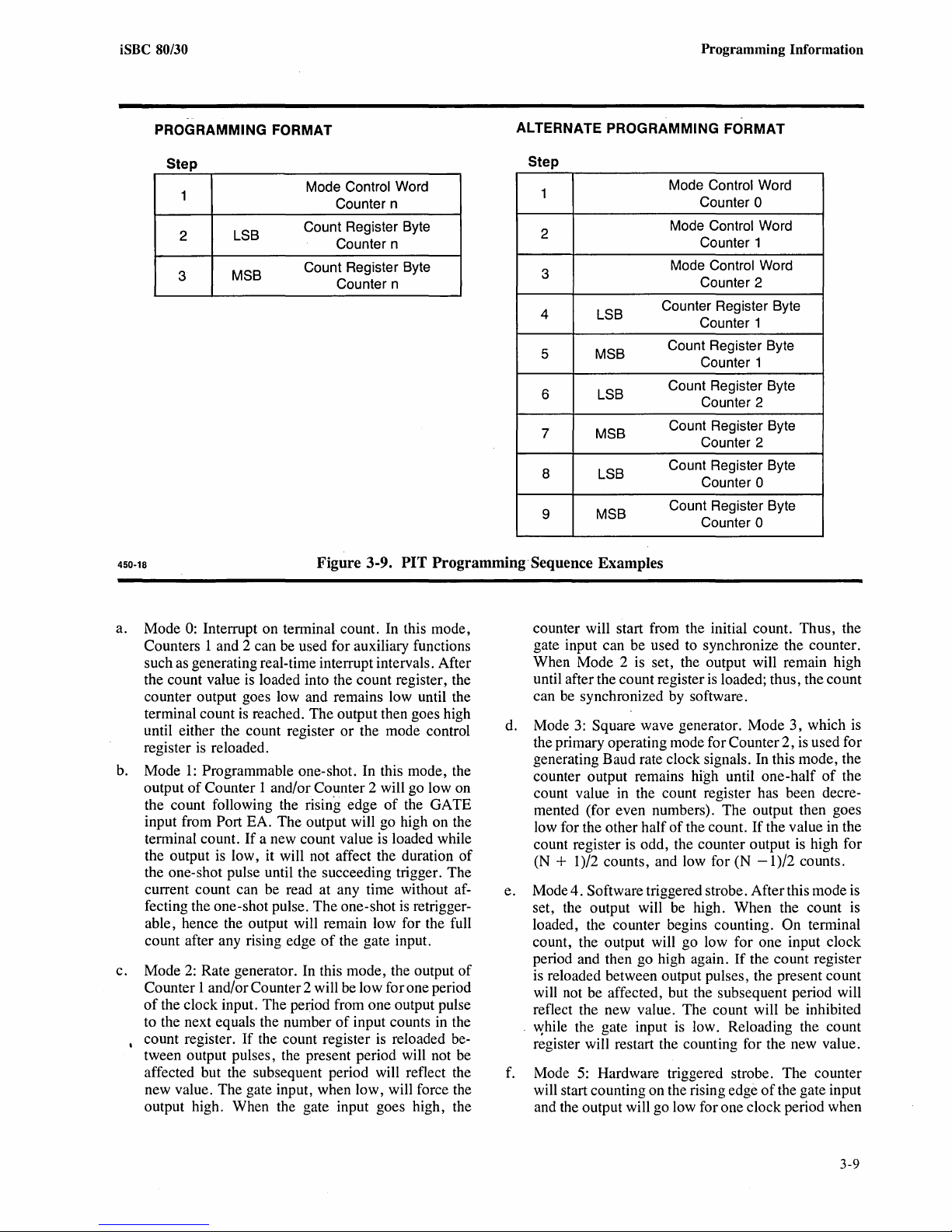
iSBC 80/30
Programming Information
PROGRAMMING FORMAT
Step
1
2
3
LSB
MSB
Mode Control Word
Count Register Byte
Count Register Byte
Counter n
Counter n
Counter n
ALTERNATE PROGRAMMING FORMAT
Step
1
2
3
4
LSB
5 MSB
6
7
8
9
450-18 Figure 3-9. PIT Programming"Sequence Examples
LSB
MSB
LSB
MSB
Control Word
Mode
Counter
Mode
Counter 1
Mode Control Word
Counter 2
Counter Register Byte
Counter 1
Count Register Byte
Counter 1
Count Register Byte
Counter 2
Count Register Byte
Counter 2
Count Register Byte
Counter
Count Register Byte
Counter
0
Control Word
0
0
a. Mode
0:
Interrupt on tenninal count. In this mode,
Counters 1 and 2 can be used for auxiliary functions
such as generating real-time interrupt intervals. After
the count value is loaded into the count register, the
counter output goes low and remains low until the
is
terminal count
until either the count register
reached. The output then goes high
or
the mode control
register is reloaded.
b. Mode
1:
Programmable one-shot. In this mode, the
output
of
Counter 1 and/or Counter 2 will go low on
the count following the rising edge
of
the GATE
input from Port EA. The output will go high on the
If
tenninal count.
a new count value is loaded while
the output is low, it will not affect the duration
the one-shot pulse until the succeeding trigger. The
current count can be read at any time without affecting the one-shot pulse. The one-shot
is
able, hence the output will remain low for the full
of
count after any rising edge
c. Mode
2:
Rate generator. In this mode, the output
the gate input.
Counter 1 and/or Counter 2 will be low for one period
of
the clock input. The period from one output pulse
of
to the next equals the number
• count register.
If
the count register is reloaded be-
input counts in the
tween output pulses, the present period will not be
affected but the subsequent period will reflect the
new value. The gate input, when low, will force the
output high. When the gate input goes high, the
retrigger-
of
counter will start from the initial count. Thus, the
gate input can be used to synchronize the counter.
When Mode 2 is set, the output will remain high
is
until after the count register
loaded; thus, the count
can be synchronized by software.
d. Mode
3:
Square wave generator. Mode
the primary operating mode for Counter 2, is used for
generating Baud rate clock signals. In this mode, the
counter output remains
count value
in
the count register has been decre-
high until one-half
mented (for even numbers). The output then goes
of
of
low for the other half
the count.
count register is odd, the counter output is high for
+ 1)/2 counts, and low for (N
(N
e. Mode
4.
Software triggered strobe. After this mode is
If
-1)/2
set, the output will be high. When the count is
loaded, the counter begins counting.
count, the output will go low for one input clock
If
period and then go high again.
the count register
is reloaded between output pulses, the present count
will not be affected, but the subsequent period will
reflect the new value. The count will be inhibited
~hile
the gate input is low. Reloading the count
register will restart the counting for the new value.
f. Mode 5: Hardware triggered strobe. The counter
will start counting on the rising
edge
and the output will go low for one clock period when
3,
which is
of
the
the value in the
counts.
On tenninal
of
the gate input
3-9
Page 52

Programming Information
iSBC 80/30
the terminal count
is
reached. The counter
is
re-
triggerable; the output will not go low until the full
of
count after the rising edge
-7
Table 3
provides a summary
versus the gate inputs; The gate inputs to Counters
are tied high by default jumpers; these gates may
the gate input.
of
the counter operation
0 and 2
optionally be controlled by Port EA. The gate input to Counter 2
is floating high and not optionally controlled.
Table 3-7. PIT Counter Operation Vs. Gate Inputs
Modes
~
tatus
0
1
2
-
Low
Or
Going
Low
Disables
counting
-
1)
Disables
counting
2) Sets output
high
immediately
Rising High
-
1)
Initiates
counting
2)
Resets output
after next clock
Initiates
counting
Enables
counting
-
Enables
counting
3-18. ADDRESSING
As listed in table 3-2, the PIT uses four consecutive I/O
addresses: DC through DF. Addresses DC, DD, and DE,
respectively, are used in loading and reading the count in
Counters
0, 1, and 2. Address
DF
is used in writing the
mode control word to the desired counter.
3-19. INITIALIZATION
To initialize the PIT chips, perform the following:
a. Write mode control word for Counter
that all mode control words are written to DF, since
mode control word must specify which counter is
being programmed. (Refer
to
figure 3-8.) Table 3-8
provides a sample subroutine for writing mode
trol words to all three counters.
b. Assuming mode control word has selected a 2-byte
load, load least-significant byte
o at DC. (Count value to be loaded
paragraphs 3-22 through 3-24). Table 3-9 provides a
sample subroutine for loading 2-byte count value.
c. Load most-significant byte
at DC.
of
0 to DF. Note
con-
of
count into Counter
is
described in
count into Counter 0
3
4 Disables
5
1)
Disables
counting
2)
Sets output
high
immediately
counting
-
;INTIMR
;COUNTERS 0 AND 1 ARE INITIALIZED
;COUNTER 2 IS INITIALIZED AS BAUD RATE GENERATOR.
;ALL THREE
;USES-NOTHING;
INTIMR:
Initiates
counting
Enables
counting
Be sure to enter the downcount in two bytes
the counter was programmed for a two-byte
entry in the mode control word. Similarly,
-
Initiates
counting
Enables
counting
-
enter the downcount value in BCD
was so programmed.
d. Repeat steps a, b, and c for Counters 1 and 2.
Table 3-8. Typical PIT Control Word Subroutine
INITIALIZES COUNTERS
COUNTERS ARE SET UP FOR 16-81T OPERATION.
DESTROYS-A.
MVI
OUT
MVI
OUT
MVI
OUT
RET
A,30H
ODF
A,70H
ODF
A,
B6H
ODF
0,
1,
2.
AS
INTERRUPT TIMERS.
;MODE CONTROL WORD FOR COUNTERO
;MODE CONTROL WORD FOR COUNTER
;MODE CONTROL WORD FORCOUNTER2
NOTE
if
1
if
the counter
END
3-10
Page 53

iSBC
80/30
Programming Information
Table 3-9. Typical
;LOADO LOADS COUNTER 0 FROM D&E,D IS MSB, E IS LSB.
;USES-D,E; DESTROYS-A.
LOADO: MOV
OUT
MOV
OUT
RET
END
PIT
A,E
ODC
A,D
ODC
3-20. OPERATION
The following paragraphs describe operating procedures
for a counter read, clock frequency divider/ratio
tion, and interrupt timer count selection.
3-21.
COUNTER
can be used to read the contents
The first method involves a simple read
READ. There are two methods that
of
a particular counter.
of
counter. The only requirement with this method
order
to
ensure a stable count reading, the desired counter
must be
inhibited by controlling its gate input. Only
Counter 0 and Counter 1 can be read using this method
because the gate input to Counter 2
is
not controllable.
The second method allows the counter to be read
the-fly." The recommended procedure
control word to latch the contents
this ensures that the count reading
The latched value
of
the count can then be read.
is
to
of
the count register;
is
accurate and stable.
NOTE
If
a counter is read during count, it
to
complete the read procedure; that is, if two
is
mandatory
bytes were programmed to the counter, then
two bytes
must be read before any other opera-
tions are performed with that counter.
To read the count
follows (a typical counter read subroutine
of
a particular counter, proceed
is
3-10):
selec-
the desired
is
that, in
"on-
use a mode
as
given in table
Count
Value Load Subroutine
;GET LSB
;GET MSB
a. Write counter register latch control word (figure
3-10)
to
DF. Control word specifies desired counter
and selects counter latching operation.
b.
Perform a read operation
of
desired counter; refer to
table 3-2 for counter addresses.
NOTE
Be sure
to
read one
or
two bytes, whichever
was specified in the initialization mode control
word. For two bytes, read in the order specified.
3-22.
SELECTION.
timer input frequencies to Counters
CLOCK
FREQUENCY
IDIVIDE
Table 2-4 lists the default and optional
0 through 2. The timer
input frequencies are divided by the counters to generate
the
8041/8741 Event Clock (Counter 0), Count Out
(Counter 1), and the 8251A Baud Rate Clock (Counter2).
Each counter must be programmed with a downcount
number,
or
count value N. When count value N
into a counter, it becomes the clock divisor. To derive
for either synchronous
tion,
use
the
or
asynchronous RS232C opera-
procedures
describ~d
in
paragraphs.
3-23. Synchronous Mode. In the synchronous mode, the
TXC and/or RXC rates equal the Baud rate. Therefore,
the count value is determined by
N = C/B
RATIO
is
loaded
N
following
Table
;READ1 READS COUNTER 1 ON-THE-FL Y INTO D&E. MSB
;USES-NOTHING; DESTROYS-A,D,E.
READ1: MVI
OUT
IN
MOV
IN
MOV
RET
END
3-10. Typical
A,40H
ODF
ODD
E,A
ODD
D,A
PIT
Counter
;MODEWORD
;LSB
OF
COUNTER
;MSB
OF
COUNTER
Read
Subroutine
IN
D,
LSB IN
E.
FOR LATCHING COUNTER 1 VALUE
3-11
Page 54

Programming Information
I
SC11
sca
I a I a I x I x I x
I'
L " L Don"t Care
Selects Counter Latching
Operation
Specifies Counter to be Latched
Figure 3-10. PIT Counter Register
450·19A
where N
Latch Control Word Format
is
the count value,
is
the desired Baud rate, and
B
C is 1.23 MHz, the input clock frequency.
,
NOTE
During initialization, be sure to load the count
value (N) into the appropriate counter and the
Baud
rate
USART.
Table 3-11.
multiplier
PIT
Count Value
(M) into the 8251 A
Vs
Rate Multiplier for
Each Baud Rate
Baud Rate
(8)
75
110
150 8192 512 128
300 4096 256 64
600 2048 128 32
1200 1024 64 16
2400
4800 256 16
9600 128 8
19200 64 4
38400 32 2
76800 16
M = 1
16384
11171
512
*Count
Value (N) For
M=16
1024 256
698 175
32 8
iSBC 80/30
M=64
4
2
Thus, for a
(N)
is:
If
the binary equivalent
into Counter 2, then the output frequency
which
operation.
3-24. ASYNCHRONOUS MODE. In the asynchronous
mode, the TXC and/or RXC rates equal the Baud rate
times one
Therefore, the count value is determined by:
4800 Baud rate, the required count value
1.23 X
N
is
the desired clock rate for synchronous mode
of
the following multipliers:
6
10
4800 ----.:
= 256
of
count value N = 256
Xl,
is
is
4800 Hz,
X16,
loaded
orX64.
N = C/BM
where
N
is
the count value,
B is the desired Baud rate,
M
is
the Baud rate multiplier (1, 16,
C is 1.23 MHz, the input clock frequency.
Thus, for a
If
the binary equivalent
into Counter 2, then the output frequency
Hz, which is the desired clock rate for asynchronous mode
operation. Count values (N) versus rate multiplier (M) for
each Baud rate are listed in table 3 -11.
4800 Baud rate, the required count value (N)
1.23 X
N = 4800 x
10
6
16
= 16.
of
count value N = 16 is loaded
or
is
4800 x
64), and
is
16
*Count
Values
Double
Count Values (N) and Rate Multipliers (M) are in
decimal.
Count
(N) assume
Values (N)
clock
is
for
1.23
2.46 MHz clock.
MHz.
3-25. RATE GENERATOR/INTERVAL tIMER.
Table 3-12 shows the maximum and minimum rate
generator frequencies. and timer intervals for Counters
and 1 when these counters, respectively, have 1.23-MHz
and 153.6-KHz clock inputs. The table also provides the
maximum and minimum generator frequencies and time
intervals and may be obtained by connecting Counters
and 1 in series.
3-26. INTERRUPT TIMER. To program an interval
timer for an interruption terminal count, program the
appropriate timer for the correct operating mode (Mode
in the control word. Then load the count value (N), which
is derived by
N = TC
where
N is the count value for Counter
T
is
the desired interrupt time interval in seconds,
and
C is the internal clock frequency (Hz).
Table 3-13 shows the count value (N) required for several
time intervals (T) that can be generated for Counters
and
1.
0,
0)
0
0
0
3-12
Page 55

iSBC 80/30
Programming Information
Table 3-12. PIT Rate Generator Frequencies and Timer Intervals
1
0)
Maximum
614.4 kHz
53.3 msec 13 p,sec
Minimum
2.344 Hz
Rate Generator
(Frequency)
Real-Time
Interrupt
(Interval)
NOTES:
1.
Assuming a 1.23-MHz clock input
2.
Assuming a 153.6-kHz clock input.
3.
Assuming Counter 0 has 1.23-MHz clock input.
3-27. 8255A
Single Timer
(Counter
Minimum
18.75 Hz
1.63 p,sec
PPI
PROGRAMMING
The three parallel I/O ports interfaced to connector J 1 are
~ontrolled
Interface.
Ports
by
an
Intel S255A Programmable Peripheral
Port A includes bidirectional data buffers and
Band
e include
Ie
sockets for installation
of
either
input terminators or output drivers depending on the
user's application.
Default jumpers set the
Port A bidirectional data buffers to
the input mode. Optional jumpers allow the bidirectional
or
data buffers to be set to the output mode
one
of
the eight Port e bits to selectively set the Port A
bidirectional data. buffers to the input
to allow any
or
output mode.
Single Timer
(Counter
Maximum
426.67 msec
2
1)
76.8 kHz
(0
and 1 in Series)
Minimum
0.00029 Hz
p,sec
3.26
Dual Timer
3
Maximum
307.2 kHz
58.25 minutes
operating mode for Port A (ES) and the upper four bits
Port e (EA). Group B (control word bits ° through 2)
defines the operating mode for
of
four bits
Port e (EA). Bit 7
Port B (E9) and the lower
of
the control word controls
the mode set flag.
CONTROL WORD
~
07\ 0
6
4
\
Os
\ 0
03\ O2 \ 01 \
Do
I
LJ
of
Table 2-11 lists the various operating modes for the three
PPI parallel I/O ports. Note that Port A
0, 1,
or
2;
operated in Modes
can be operated
3-28.
CONTROL
in
Mode °
Port B (E9) and Port e (EA)
or
1.
WORD
FORMAT
The control word format shown in figure 3
initialize the
PPI to define the operating mode
ports. Note that the ports are separated
Group A (control word bits 3 through
Table 3-13.
PIT
Timer Intervals
T
10 p,sec
100 p,sec
1 msec
10 msec
50 msec
*Count Values
Double Count Values
clock. Count Values
(N)
assume clock is 1.23 MHz.
(N)
(N)
are
for
in
(ES)
-11
is
of
the three
into two groups.
6)
defines the
Vs
Timer Counts
N*
12
123
1229
12288
61440
2.46 MHz
decimal.
can be
used to
GROUP B
'----
/
PORT C (LOWER)
1 = INPUT
0=
OUTPUT
PORT
l'
INPUT
0=
OUTPUT
MODE SELECTION
0=
MODE 0
1 = MODE 1
GROUP A
/
PORT C (UPPER)
1 =
INPUT
0=
OUTPUT
PORTA
1 = INPUT
0=
OUTPUT
MODE SELECTION
= MODE 0
00
01
= MODE 1
MODE 2
1X =
MODE SET FLAG
ACTIVE
1 =
\
B
\
Figure 3-11. PPI Control Word Format
3-13
Page 56

Programming Information
;INT PAR INITIALIZES PARALLEL PORTS.
;USES-NOTHING; DESTROYS-A.
INT
PAR: MVI
Table 3-14. Typical PPI Initialization Subroutine
OUT
RET
END
A,92H
OEBH
;MODE WORD TO PPI PORT A&B IN,C
iSBC 80/30
OUT
3-29. ADDRESSING
The PPI uses four consecutive addresses
for data transfer, obtaining the status
for port control. (Refer to table 3-2.)
(ES
through EB)
of
Port C (EA), and
3-30. INITIALIZATION
To initialize the PPI, write a,control word
figure 3-11 and table 3-14 and assume that the control
word is 92 (hexadecimal). This initializes the
follows:
a. Mode
b.
c.
Set Flag active
Port A (ES) set to Mode 0 Input
Port C (EA) upper set to Mode 0 Output
d. Port B (E9) set to Mode 0 Input
Port C (EA) lower set to Mode 0 Output
e.
to
ES. -Refer to
PLI
as
3-31. OPERATION
After the PPI has been initialized, the operation
or
performing a read
a write to the appropriate port.
3-32. READ OPERATION. A typical read subroutine
Port A
for
3-33.
is
given in table 3-15.
WRITE
OPERATION. A typical write sub-
routine for Port C is given in table 3-16.
of
figure 3-12, and
cleared by writing a control word
the Port C bits can be selectively set
to
EB.
is
As
shown in
simply
or
3-34. 8259A PIC PROGRAMMING
As described
interrupt requests from eight separate sources. When one
or
more
determines the following:
a. Which input signal has the highest priority.
b. Whether the input signal has a higher priority than
the interrupt presently being serviced by the main
processor.
terrupted;
output.
c. Whether the interrupt input bit is masked.
Thus, the basic functions
priority
rupt request to the
that priority. The output
the INTR input
3-35. INTERRUPT
The PIC' has two modes for resolving the priority
interrupt inputs: (1) fully nested mode and (2) rotating
mode. The rotating mode has two variations: auto-rotating
and specific rotating.
3-36. FULLY NESTED MODE.
input signals are assigned priority from 0 through 7. The
PIC operates
otherwise. Interrupt
has the lowest priority. When an interrupt
ledged, the highest priority request is available to the
CPU. Lower priority interrutps are inhibited; higher prior-
in
paragraph 2-20, the PIC monitors the
of
the interrupt requests are active (true), the PIC
If
so, the interrupt being serviced
if
not, the input signal
of
the PIC are (1) resolve the
of
interrupt requests and (2) issue a single inter-
SOS5A
microprocessor (CPU) based on
of
the PIC
of
the CPU. (Refer to paragraph 3-50.)
PRIORITY
in
this mode unless specifically programmed
IRO
has the highest priority and IR
is
held for later
is
applied directly to
MODES
In
this mode the PIC
is
acknow-
is
in-
of
7-
Table 3-15. Typical PPI
;AREAD READS A BYTE FROM PORT A INTO REG A.
;USES-A;
AREAD: IN
3-14
DESTROYS-A.
RET
END
OE8H
Port
Read Subroutine
Page 57

iSBC 80/30
Programming Information
Table 3-16. Typical PPI Port Write Subroutine
;COUT OUTPUTS A BYTE FROM
;USES-A; DESTROYS-NOTHING.
COUT: OUT
RET
END
ity interrupts will be able to generate an interrupt that will
be acknowledged
if
the CPU has enabled its own interrupt
'input through software. An End-Of-Interrupt (EOI) com-
mand from the CPU is required to reset the PIC for the
next interrupt.
3-37. AUTO-ROTATING MODE. In this mode the
interrupt priority rotates. Once an interrupt on a given
input is serviced, that interrupt assumes the lowest
ty. Thus,
if
there are a number
of
simultaneous interrupts,
priori-
the priority will rotate among the interrupts in numerical
For
order.
example,
service simultaneously, IR4 will receive the highest
ity. After service, the priority level rotates
if
interrupts IR4 and IR6 request
so
that IR4 has
prior-
the lowest priority and IRS assumes the highest priority.
In the worst case, seven other interrupts are serviced
Of
before IR4 again has the highest priority.
is
the only request, it
is
serviced promptly. In the Auto-
course, ifIR4
Rotating Mode, priority shifts when the PIC chip receives
an End-of-Interrupt (EOI) command.
3-38. SPECIFIC ROTATING MODE. In this mode
the software can change interrupt priority by
the bottom priority, which automatically sets the highest
if
IRS
priority. For example,
is assigned the bottom prior-
ity, IR6 assumes the highest priority. In the specific rotat-
~pecifying
REG
A TO PORT C.
OEAH
ing mode, the priority can be rotated by writing a Specific
Rotate at EOI (SEOI) command to the PIC chip. This
command contains the BCD code
of
the interrupt being
serviced; that interrupt is reset as the bottom priority. In
addition, the bottom priority interrupt can be fixed at any
time by writing a command word to the PIC chip.
3-39. INTERRUPT MASK
One
or
more
of
the eight interrupt request inputs can be
individually masked during the PIC initialization or at any
If
subsequent time.
an interrupt is masked while it is being
serviced, lower priority interrupts are inhibited. There are
two ways to enable the lower priority interrutps:
a. Write an End-of-Interrupt (EOI) command.
Set the Special Mask Mode.
b.
The
Special Mask Mode is useful when one
interrupts are masked.
while it
is
being serviced, the lower priority interrupts are
If
for any reason an input
disabled. However, it is possible to enable the lower
priority interrupt with the
Special Mask Mode. In this
mode, the lower priority lines are enabled until the
Mask Mode is reset. Higher priorities are not affected.
3-40. STATUS READ
or
is
masked
Special
more
CONTROL WORD
L.....----------_I
Figure 3-12. PPI
Port
C Bit Set/Reset Control
Word Format
BIT
SET/RESET
1·
SET
O·
RESET
~I!
;~:g~~SET
FLAG
Interrupt request inputs is handled by the following two
internal PIC registers:
a. Interrupt Request Register (lRR) , which stores all
interrupt levels that are requesting service.
In-Service Register (lSR), which stores all interrupt
b.
levels that are being serviced.
Either register can be read by writing a suitable command
word and then performing a read operation.
3-41. INITIALIZATION COMMAND WORDS
The eight devices serviced by the PIC have eight
ses equally spaced in memory that can be programmed at
of
four
or
intervals
eight bytes. Interrupt service routines
for these eight devices thus occupy a 32- or64-byte block,
of
respectively,
interrutp service routine
memory. The address format for device
is
shown in figure 3-13.
addres~
3-15
Page 58

Programming Information
iSBC 80/30
(4) Bit 1 specifies whether
0'
~
6
A7 I A6 I As A4
'---.---l-
DEFINED BY 05-7 OF ICW'
~~--------------v~------------~)
Os
--
j\
DEFINED BY
0
4
Figure 3-13. PIC Device
O2 0
0
3
A2
A3
v
AUTOMATICAllY
INSERTED BY 8259
ICW2
Interrupt
1
Al
Addresses
Do
AO
I
)
(5) Bits 0 and 4 identify the word
b.
The second word (lCW2) specifies the upper byte
(bits 8-15)
3-42. OPERATION COMMAND WORDS
After being initialized, the PIC can be programmed at any
time for various interrupt modes. The Operation Command Word
discussed in paragraph 3 -45.
Bits 0-4 are automatically inserted
6-15 are programmed by Initialization Command Words
ICWI and ICW2.
5
is
automatically inserted by the PIC; if the address
if
interval
four bytes, bit 5
the 32-byte
If
the address interval
or
64-byte block
is
by
the PIC whereas bits
is
eight bytes, bit
programmed
of
in
addresses reserved for
ICWI.
Thus,
3-43. ADDRESSING
The PIC uses two consecutive addresses for writing to and
reading internal registers. Address functions pertinent to
programming are identified in table 3 -2.
interupt service routines can be located anywhere in the
available memory space. Table 3-17 shows the address
format inserted by the
PIC for each device.
3-44. INITIALIZATION
To initialize the PIC, proceed
of
Initialization
8-bit Initialization Command words
3 -14. Since there are no slave
the one
PIC consists
mand Words
the PIC consists of writing two or three
as
shown
in
PIC's, the initialization for
of
writing two Initialization Com-
as
follows:
figure
a. The first Initialization Command Word (lCW1) con-
of
sists
(1) Bits 5-7 specify the most-significant bits
the following:
lower address byte
of
the interrupt service
of
the
provides a typical initialization subroutine);
a. Disable system interrupts
Interrupts) instruction.
b.
Write ICWI to D8.
c. Write ICW2 to D9.
d.' Enable system interrupts by executing an
Interrupts) instruction.
routine.
(2) Bit 3 establishes whether the interrupts are re-
quested by a positive-true
or
requested by a
low-to-high transition input. This applies to all
by
input requests handled
words,
if
bit 3-1, a low-to-high transition
required to request
eight levels ,handled by the
(3)
Bit
2 specifies a 4-byte
an
the PIC. In other
interrupt on any
PIC.
or
8-byte address
of
the
interval.
is
The PIC operates in the fully nested mode after
the initialization sequence without requiring any
Operation Control Word (OCW).
3-45. OPERATION
After initialization, the PIC chips can be
any time for the following operations:
or
not there are slave
(cascaded)
set bit 1
PIC's. Since there are no slave
==
l.
of
the interrupt service routine.
as
ICWl.
(OCW) formats are shown in figure 3-15 and
as
follows (table 3-17
by
executing a DI (Disable
EI
(Enable
NOTE
progr~mmed
PIC's,
at
Device
D7
D6
IR7
IR6
,
IR5
IR4
IR3
IR2
IR1
IRO
3-16
A7
A7
A7
A7
A7
A7
A7
A7
A6
A6
A6
A6
A6
A6
A6
A6 A5
D5
A5
A5
A5
A5
A5
A5
A5
Interval
.D4
1
1
1
1
0 1
0 1
0
0
Table 3-17. PIC Device Address Insertion
Lower Routine Address Byte
= 4
D3
D2
Dl
1
1
0 1
0
0
0
1
0 0
0 0 0
0
0
0
1
0
0
0
1
0
0 0 0
DO
0
0
0
0
0
D7 D6
A7
A7
A7 A6
A7 A6
A7
A7
A7
A7 A6
A6
A6
A6
A6
A6
D5
1 1 1
1 1
1
1
0 1 1
0
0 0 1
0 0 0
Interval = 8
D4
D3 D2
0
1
0
0 0 0
1
0
Dl
DO
0 0
0
0
0
0
0
0
0
0
0 0
0 0
0 0
0 0
0 0
0 0
0
Page 59

iSBC 80/30
07 0
6
07 0
6
ICW'
ICW2
Os
D. 0
3
ICW3 (MASTER DEVICEI
Os
D.
0
3
O2 0,
Programming
Information
a. Auto-rotating priority.
b. Specific rotating priority.
of
Interrupt Request Register (lRR).
of
In-Service Register (lSR).
or
reset.
of
the above operations. Note that
or
a Special End-Of-Interrupt
is
required at the end
of
each interrupt
EOI command
is
sued
,.
SINGLE
O'
NOT SINGLE
CALL
ADDRESS
, •
O'
1
o = EDGE TRIGGERED
INTERVAL
INTERVAL
IS 4
INTERVAL
IS 8
.~
LEVEL TRIGGERED
c. Status read
d. Status read
e. Interrupt mask bits set, reset, or read.
f.
Special mask mode set
Table 3 -19 lists details
End-Of-Interrupt (EOI)
an
(SEOI)
command
service routine to reset the ISR. The
in the fully nested and auto-rotating priority modes and
A7_5 OF LOWER
ROUTINE ADDRESS
the SEDI command, which specifies the bit to be reset,
used in the specific rotating priority mode. Tables 3-20
is
through 3-24 provide typical subroutines for the following:
DO
a. Read IRR (table 3-20).
b. Read ISR (table 3-21).
UPPER
ADDRESS
ROUTINE
c. Set mask register (table 3-22).
d. Read mask register (table 3-23).
e. Issue
EOI command (table 3-24).
L---'----L_.,..&-----L.._'----'----L_-f
07 0
, 0 I 0 I 0 I 0 I 0
! ! !
I
ICW3 (SLAVE DEVICE)
Os
6
I
I
DON'T
CARE
D. 03 O2 0,
!
!
I I
11D2
DO
lID, I IDol
,
O'
Figure 3-14. PIC Initialization Command
611·8
Word Formats
Table 3-18. Typical PIC Initialization Subroutine
;INT59 INITIALIZES THE PIC. A 64-BYTE ADDRESS BLOCK BEGINNING WITH
;4000H IS
MASK IS SET, DISABLING ALL PIC INTERRUPTS.
;PIC
;USES·SMASK; DESTROYS-A.
INT59:
• IR INPUT HAS A SLAVE
IR INPUT DOES NOT
A SLAVE
HAVE
3-46. 8041/8741A UPI PROGRAMMING
Table 3-2 lists the addresses used 'for writing data and
commands and
Jor
bly language programming information for the Intel
SLAVE
10
o ,
2 3 4 5 6 7
o 1
o 0 1 1 0 o 1 1
o 0 0 o 1
o 1 0
1 0 1
, 1
,
8041/8741A is given in the
Order No. 9800504, and Control With UPI-41 , Application Note AP-27.
Figure 3 -16 illustrates the internal configuration
UPI data bus buffer and status register. The CPU accesses
UPI data bus buffer register via I/O Read and Write
the
Commands to E4
VO
via an
~--
...
SET UP FOR INTERRUPT SERVICE ROUTINES.
EXTRN
CALL
MVI
OUT
MVI
OUT
MVI
CALL
RET
SMASK
SETD
A,12H
OD8H
A,40H
OD9H
OFFH
SMASK
;ICW1
;ICW2TO
or
Read Command to E5
TO PIC
PIC
reading
data_
and status words. Assem-
Intel UPI-41 User's Manual,
of
E6. The CPU accesses the UPI status
or
E7.
the
END
3-17
Page 60

Programming Information
iSBC 80/30
07 0,
07 0
I R I
6
SEOI I EOI
OCWI
0
D. 0
5
OCW2
Os
D.
I 0 I 0 I
O2 0,
3
03 O2 0,
L2 I L, 1 Lo
DO
DO
I
J
BCD
LEVEL TO
BE
OR
PUT
INTO
2 3 4 5
0
1
0 1 0
0 0 1
0 0 0 0 1
NON-SPECIFIC
1 - RESET THE HIGHEST PRIORITY
BITOF
ISR
0-
NO ACTION
SPECIFIC
1 - L2.
L,.
0-
NO
ACTION
LOWEST
1 0 1
1
END
END
Lo
0 0
OF
OF
INTERRUPT
BITS ARE
RESET
PRIORITY
6
0
1 1
1 1
1
INTERRUPT
USED
7
1
07 0
6
I -IESMMI
DoLT
CARE
OCW3
Os
D. 03 O2 0,
SMM
I 0 I 1 I
Do
P I ERIS I RIS I
I
:
ROTATE PRIORITY
1-
ROTATE
O-NOTROTATE
READ IN-SERVICE REGISTER
1 0
0
I
0
I
NO ACTION
POLLING
A HIGH ENABLES THE NEXT
TO READ THE
EST
LEVEL REOUESTING INTERRUPT_
SPECIAL MASK MODE
0
I
0
I
NO ACTION
1 1
0
READ READ
IR
REG
ON
NEXT
RDPULSE RDPULSE
BCD
CODE
1 0 1
1 1
0
RESET
SPECIAL
MASK
1
ISREG
ON
NEXT
AD
PULSE
OF THE HIGH-
SET
SPECIAL
MASK
Figure 3-15. PIC Operation Control Word Formats
3-18
Page 61

iSBC 80/30
Programming Information
Table 3-19. PIC Operation Procedures
Operation
Auto-Rotating
Priority Mode
Specific Rotating
Priority Mode
Procedure
To set:
In
OCW2, write a Rotate Priority at EOI command
Terminate interrupt and rotate priority:
In
OCW2, write EOI command (20H) to 08.
To set:
In
OCW2, write a Rotate Priority at SEOI command
07
I
BCOof
To terminate interrupt and rotate priority:
In
OCW2, write an SEOI command
I
06
1
1
1 1
I
IR
line
to
in
the following format
07 I 06 I 05 I 04 I 03 I 02
o o
I
BCO
of ISR flip-flop
To rotate priority without
In
OCW2, write a command word
EOI:
07
I
1
BCO
of bottom priority
in
the following format to 08.
06 I 05 I 04 I 03 I 02 I 01 I 00
rr
-------------------------~~y~----~
(AOH)
to
08.
in
the following format to
0
to
be reset.
o
IR
1
line.
03
0
o
o
1
02
I
01
,"L~.
to
08.
I 01 I
L2
......
"L2
L1
---y--""
L 1
I
00
00
05 1 04
1
be reset and/or put into lowest priority.
o
08:
LO
LO
I
1
I
,
Interrupt Request
Register
Status
In-Service
Register (ISR)
Status
(IRR)
IRR stores a
The
an
interrupt. To read the IRR (refer to footnote):
(1)
Write
(2) Read 08. Status format
The ISR stores a
The
ISR is updated when an EOI command
to footnote):
(1) Write
(2)
Read 08. Status format
Be sure
to
Auto-Rotating (both types) and
"1"
in
the associated bit for each IR input line that is requesting
OBH
to 08.
IR
Line: 7
"1"
in
OAH
to
08.
IR
Line: 7
reset ISR bit at end-of-interrupt when
is
as
follows:
1 071
the associated bit for priority inputs that are being serviced.
I
I
06
6
is
as follows:
07
06
1
6
Special Mask. To reset ISR
071 06 I 05
0
1
I,
BCO identifies bit
05 1 04
1
5
is
05 1 04
1
5 4 3
in
04 1 03 I 02
I
1
to
be
01
1 031
4
issued. To read the ISR (refer
1 031
the following modes:
0
02
3 2
02
in
0
L2
I
1
2
OCW2, write:
1 01
"
reset.
01
L1
-y-
00
I
1
0
001
1
1
0
00
1
LO
-
I
1
."
3-19
Page 62

Programming Information
iSBC 80/30
Table 3-19. PIC Operation Procedures (Continued)
Operation
Interrupt Mask To set mask bits
Register
IR
1 = Mask Set, o = Mask Reset
To read mask bits, read
Special Mask Mode enables desired bits that have been previously masked;
Special
Mask
Mode lower priority bits are also enabled.
NOTE:
If
previous operation was addressed to same register, it is not necessary to rewrite the OCW.
The
To set, write 68H to 08.
To reset, write 48H
in
Bit Mask:
Procedure
OCW1, write the following mask byte to
I
07
I
D~
1051 041 031
MS
to
M7 M6
09.
08.
Table 3-20. Typical PIC Interrupt Request Register Read Subroutine
;RRO
READS PIC INTERRUPT REQUEST REGISTER.
;USES-NOTHING; DESTROYS-A.
M4
09:
02
M3 M2
01 1 DO
I
M1
I
MO
RRO:
MVI
OUT
IN
RET
END
A,OAH
OD8H
OD8H
;OCW3 RR INSTRUCTION TO PIC
Table 3-21. Typical PIC In-Service Register Read Subroutine
;RISO
READS PIC IN-SERVICE REGISTER.
;USES-NOTHING; DESTROYS-A.
RISO:
MVI
OUT
IN
RET
END
A,08H
OD8H
OD8H
;OCW3 RIS INSTRUCTION TO PIC
Table 3-22. Typical PIC Set Mask Register Subroutine
;SMASK STORES A REG INTO PIC MASK REGISTER.
;A ONE MASKS OUT
;USES-A; DESTROYS-NOTHING.
SMASK:
OUT
RET
AN
INTERRUPT, A ZERO ENABLES IT.
OD9H
3-20
END
Page 63
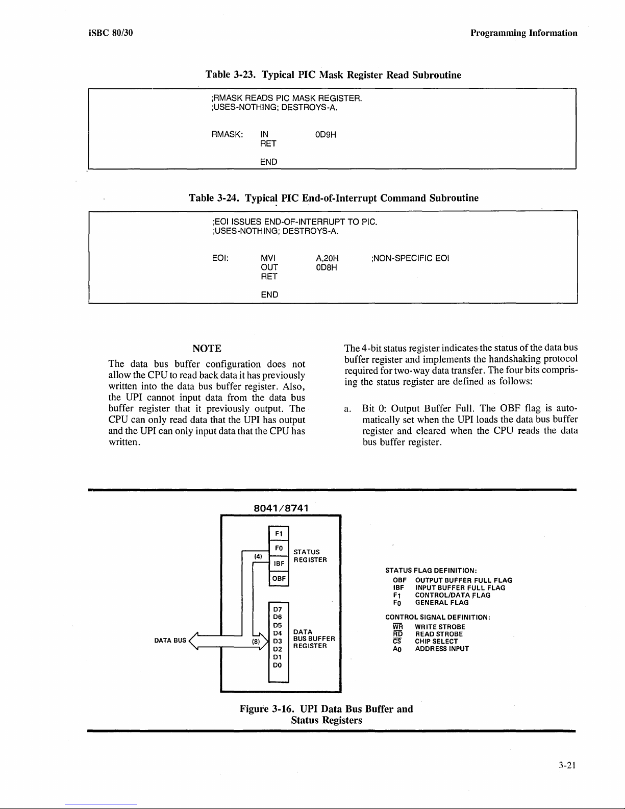
iSBC
80/30
Programming Information
Table 3-23. Typical PIC Mask Register Read Subroutine
;RMASK READS PIC MASK REGISTER.
;USES-NOTHING; DESTROYS-A.
RMASK:
IN
RET
END
Table 3-24. Typica! PIC End-of-Interrupt Command Subroutine
;EOI ISSUES END-OF-INTERRUPT TO PIC.
;USES-NOTH ING; DESTROYS-A.
EOI:
MVI
OUT
RET
END
NOTE
The data bus buffer configuration does not
CPU
to
allow the
read back data it has previously
written into the data bus buffer register. Also,
UPI cannot input data from the data bus
the
buffer register that it previously output. The
CPU can only read data that the UPI has output
and the
UPI can only input data that the CPU has
written.
GOgH
A,2GH
;NON-SPECIFIC EOI
GD8H
The 4-bit status register indicates-the status
buffer register and implements the handshaking protocol
required for two-way data transfer. The four bits compris-
as
ing the status register are defined
a. Bit
0:
Output Buffer Full. The OBF flag
follows:
matically set when the UPI loads the data bus buffer
register and cleared when the
CPU reads the data
bus buffer register.
of
the data bus
is
auto-
DATA
BUS
8041/8741
(4)
STATUS
REGISTER
DATA
BUS
BUFFER
REGISTER
STATUS FLAG DEFINITION:
CONTROL SIGNAL DEFINITION:
Figure 3-16. UPI Data Bus Buffer
Status Registers
OBF OUTPUT BUFFER FULL FLAG
IBF INPUT BUFFER
Fl
CONTROL/DATA ,FLAG
FO
GENERAL FLAG
WR WR
RD
CS
AO
ITE STROBE
READ STROBE
CHIP SELECT
ADDRESS INPUT
FULL
FLAG
and
3-21
Page 64

Programming Information
Table 3-25. Typical UPI Data Byte Read Subroutine
;IN41
READS DATA
, ;USES-NOTHING; DESTROYS-A.
IN41:
IN
ANI 1
JZ
IN
REf
END
BYTE
OE5H
IN41
OE4H
FROM UPI.
;INPUT STATUS
;CHECK OBF
;WAIT
FLAG
IF EMPTY
iSBC 80/30
Table 3-26. Typical UPI
;OUT
41
:USES-NOTHING; DESTROYS-A.
OUT41:
b. Bit I: Input Buffer Full. The IBF flag
WRITES DATA
IN
ANI
JZ
OUT
REf.
END
is
set when the
OE5H
2
OUT41
OE4H
CPU writes a character to the data bus buffer register
and cleared when
the UPI inputs the -contents-6fthe
data bus buffer register to its accumulator.
c. Bit
2:
cleared
FO.
This general purpose flag, which can be
or
toggled under UPI software control,
used to transfer UPI status information to the CPU.
d. Bit
3:
dition
FI
(Control/Data). This flag
of
the
AO
input line when the CPU writes a
is
set to
thecon-
character to the data bus buffer register. This flag
or
can be cleared
Tables
3-25 and 3-26, respectively, provides typical
toggled under UPI software control.
routines for inputting and outputting a data byte from and
UPI.
to the
3-47. INTERRUPT HANDLING
The iSBC 80/30 includes fige interrupt inputs: TRAP,
RST 7.5, RST 6.5, RST 5.5, and INTR. The three
start" interrupts (7.5, 6.5, and 5.5) are maskable; the
TRAP is also a "restart" interrupt but
RST 7.5, RST 6.5, and RST 5.5 interrupts cause the
The
internal execution
are enabled and
previously executed
of
an
RST instruction
if
the interrupt mask
SIM instruction. The nonmaskable
TRAP interrupt causes the execution
is
nonmaskable.
if
the·
is
not set by a
of
an RST instruc-
"re-
interrupts
Data
Byte Write Subroutine
BYTE
TO UPI.
;INPUT STATUS
;CHECK IBF
;WAIT
tion independent
FLAG
IF NOT READY
of
the state
of
the interrupt enable
interrupt mask. The priority and vector location
the restart interrupts are given in table 3-27.
Table 3-27. 8085A
is
Interrupt
TRAP
CPU Restart
Vector
Location
24 Highest
RST 7.5
RST 6.5 34 3rd
RST 5.5
3C 2nd
2C 4th
Interrupt
3-48. TRAP INPUT
There are special considerations that must be understood
when the TRAP
interrupt
inte~pt
is
nonmaskable can present problems in at least
two areas.
Interrupt driven systems often contain parameters that
must be modified only within critical regions. A critical
region can be roughly defined
once begun must complete execution before it
critical regin that corresponds to the same system parame-
ter(s) can be executed. A TRAP interrupt handler cannot
safely alter such parameters either directly
causing the execution
such parameters.
is used. The fact that the TRAP
as
a section
or
of
procedures
or
tasks that may alter
or
of
each
Vectors
Priority
of
code that
or
another
indirectly by
of
3-22
Page 65

iSBC 80/30
Programming Information
If
the hardware generates a TRAP interrupt on power up
or
power fail, the system must be able to process the TRAP
interrupt before it is completely initialized. It should also
take into account that an interrupt routine that runs with
interrupts disabled can still be interrupted by a TRAP.
Because
of
these considerations, it is recommended that
the TRAP interrupt only be used for system startup and/or
catastrophic error handling.
It
should be noted that TRAP does not destroy a previously established interrupt enable status. Executing the
first RIM instruction
the interrupt enable status
occurred. Following this first
followip.g a TRAP interrupt yields
as
it
was before the TRAP
mandatory RIM instruction,
subsequently executed RIM instuctions provide current
interrupt enable status.
3-49. RST 7.5, 6.5, 5.5 INPUTS
These interrupts can be individually masked by a SIM
instruction and 'can thus be prevented from interrupting
the
CPU. The priorities shown in table 3-27 does not take
into account the priority
higher priority interrupt.
rupt an
before the end
The
and, in order
RST 7.5 routine if the interrupts are re-enabled
of
RST 6.5 and 5.5 interrupts are high level sensitive
to
of
a routine that was started by a
An
RST 5.5 interrupt can inter-
the RST 7.5 routine.
be recognized, must remain high. The
RST 7.5 interrupt
is
required
remembered until the request
is
rising edge sensitive and only a pulse
to
set the interrupt request; this request will be
is
serviced
or
reset by a SIM
instruction.
The TRAP interrupt, which
is
both edge and level sensi-
tive, must have a leading (positive-going) edge and then
remain high until serviced.
3-50. INTR INPUT
The INTR input from the 8259A PIC has the lowest
priority and is sampled only during the last clock cycle
given instruction. When INTR
ram Counter (PC)
INTN
pulses, are transferred from the PIC to the CPU:
is inhibited and three bytes, timed by
is
active, the CPU Prog-
a. Byte 1 = CALL instruction (11001101)
b.
Byte 2 = Lower byte
c. Byte 3
= Upper byte
of
routine address
of
routine address.
The 16-bit routine address must be on a 32-byte boundard
or
64-byte boundary
as
determined by the Initialization
Command Words previously written to the PIC. (Refer
paragraph 3-41.)
The INTR
abled
by
enabled
"reset"
or
disabled by software. It
and immediately after an interrupt is
is
accepted.
of
is
dis-
a
to
3-23/3-24
Page 66

CHAPTER
4·
PRINCIPLES OF OPERATION
4-1. INTRODUCTION
This chapter provides a functional description and a cir-
of
cuit analysis
Figures 4
simplified foldout block diagrams that illustrate the functional interface between the
(CPU) and the on-board facilities and between the
and the system facilities via the Multibus. Also shown in
4-2
figure
iSBC 80/30 to function in a master/slave relationship with
the Multibus to allow another bus master to access the
on-board RAM.
the iSBC 80/30 Single Board Computer.
-1
and 4 -
2,
located at the end
is the dual port control logic that allows the
8085A
of
this chapter, are
microprocessor
CPU
4-2. FUNCTIONAL DESCRIPTION
A brief description
iSBC 80/30 is given in following paragraphs. An
the
operational circuit analysis is given beginning with parag-
raph 4-14.
4-3. CLOCK CIRCUITS
The clock circuit composed
stabilizedby a 22.1184-MHz crystal. This circuit, which
provides the various clock frequencies required for onboard activities, generates a power-up Reset signal to
initialize the system to a known internal state; a Reset
signal can also be initiated by a signal supplied via aux-
iliary connector P2.
The clock circuit composed
by an 18.432-MHz crystal. This frequency is divided by
two to provide the
Constant Clock (CCLK/)
is
signal
jumpers are provided to allow this on-board clock circuit
to be disabled
CCLK/ to the Multibus.
also used by B us Controller A67 .) Removable
of
the functional blocks comprising
of
A12, A13, and A21 is
of
A55 and A57
9.22-MHz
if
some other source supplies BCLK/ and
Bus Clock (BCLK/) and
to
the Multibus. (The BCLK/
is
stabilized
4-5. INTERVAL
The 8253 Programmable Interval Timer (PIT) includes
three independently controlled counters that provide optional (jumper selectable) timing inputs to the on-board
VO
devices and the CPU interrupts. The clock frequency
of2.46
from the clock circuit composed
provides the basic timing input.
Counter 2 provides timing for the serial
USART). This counter, in conjunction with the USART,
can provide programmable Baud rates from 110
Counter 0 can be used as a timing input to the optional
8041/8741
its own internal timer input. Counter
an optional UPI, can be used as an interval timer to
generate a
interval timer and can also generate a
range
longer times are required, Counters 0 and 1 can be cascaded
more than 50 hours.
MHz,
UPI which, in tum, can connect this signal to
CPU interrupt. Counter 1, which is the system
of
1.6 microseconds to 853.3 milliseconds.
to
provide a single timer with a maximum delay
1.23
TIMER
MHz,
or
153.6 kHz, which
of
A12, A13, and A21,
0,
if
CPU interrupt, has a
is
derived
VO
port (8251 A
to
9600.
not employed by
of
4-6. SERIAL I/O
The
8251A
Receiver/Transmitter (USART) provides RS232C compatibility and is configured as a data terminal. Synchron-
or
ous
stop bits, and Baud rates are all programmable. Data,
clocks, and control lines to and from connector J3 are
buffered
A second serial
ramming the optional 8041/8741
USAR T. This second channel is limited in speed and the
number
receiver) but
CRT interface.
Universal
asynchronous mode, character size, parity bits,
with
drivers and receivers.
VO
of
RS232C interface lines (one driver and one
is
sufficient to communicate with a simple
Synchronous/Asynchronous
channel may be derived from prog-
UPI to simulate the
If
4-4. CENTRAL PROCESSOR UNIT
The,8085A Microprocessor (CPU), which
the single board computer, performs system processing
functiqns and generates the address and control signals
required to access memory and
AD7 pins are used to multiplex the 8-bit input!output data
of
and the lower eight bits
of
a machine cycle, for example, the lower eight bits
part
of
address are strobed into Latch A23 by the Address
Latch Enable (ALE) signal; the outputs
bined with the upper eight
16-bit address bus. During the remainder
cycle, ADO-AD7 pins
output.
the address. During the first
bits
of
the CPU are used for data input!
is
the heart
VO
devices. The
of
A23 are com-
of
the address to form the
of
the machine
ADO-
4-7. PARALLEL I/O
The 8255A Programmable Peripherel Interface provides
of
VO
24 programmable
included to interface eight
Two IC sockets are provided so that, depending
application, TTL drivers
led to complete the interface to connector
are grouped into three ports
can be programmed to be
ports with handshaking. One port can be programmed as a
bidirectional port with control lines. The
includes various optional features such as RS232C interface lines, timer gates, and interrupts that can be controlled by the parallel
lines. A bidirectional bus driver is
of
the
VO
lines to connector
or
VO
terminators may be instal-
n.
of
eight lines each; these ports
&imple
VO
ports
VO
lines.
on
The 24 lines
or
strobed
iSBC 80/30
n.
the
VO
4-1
Page 67

Principles of Operation
iSBC 80/30
4-8. UNIVERSAL PERIPHERAL
INTERFACE
The optionafS041/8741A Universal Peripheral Interface
is
(UPI)
faces directly to the
The UPI can interface devices such
or a keyboard scanner while relying on the
data transfer.
a complete single chip microcomputer that inter-
808SA CPU through the I/O structure.
as
a printer controller
CPU only for
4-9. INTERRUPT CONTROL
The interrupt section provides
interrupts connect to the inputs
Interrupt Controller
connect directly to the
TRAP, are maskable;. the TRAP interrupt
handle a power fail (PFI/) signal input via auxiliary con-
P2.
nector
There are
UPI (1), USAR T (2), PIT (2), external via
power fail via
4-10~
IC sockets A25 and A37 are provided for user installation
of
modate either
EPROM
normally reserved for
ROMiEPROM may be disabled through an optional
jumper connect on the 8255A
18
jumper-selectable interrupt sources: PPI (2),
ROM/EPROM CONFIGURATION
ROM/EPROM chips. Jumpers are provided to accom-
address space begins at 0000. This space is
(PIC);.
8085A CPU. All interrupts, except
P2 (1), and Multibus (8).
lK,
2K,
ROM/EPROM use only; however,
12
priority interrupts. Eight
of
the 8259 Programmable
the"
remaining four interrupts
or
4K
chips. The on-board ROM/
PPI output port.
is
intended
11
and J2 (2),
to
4-11. RAM CONFIGURATION
The iSBC 80/30 includes 16K
plemented with eight Intel 2117 chips and an Intel
Dynamic RAM Controller. Dual-port control logic interfaces this RAM with the Multibus
can perform as a slave RAM device when not acting
bus master. The slave RAM decode logic allows
Multibus addressing
bus masters with
the iSBC
I-megabyte address space. The
has only a 16-bit address capability and the 16K RAM
must reside in a 64K address space. Hardware jumpers
allow the
16K
80/30 into any 8K
8085A CPU
of
on-board RAM.
of
up to 20 address lines. This allows
20-bit addressing capability to partition
or
the system to access either 8K
of
dynamic RAM im-
8202
so
that the iSBC 80/30
as
exte~ded
or
16K segment in a
8085A CPU, however,
or
4-12. BUS INTERFACE
4-13. DUAL
The dual-port control logic allows the iSBC 80/30 to
function as a slave RAM device when not acting as a bus
master. The dual-port control logic enables
internal data and address buses, depending on whether the
access is from the
RAM access, the
request.
An extended addressing facility
16K RAM to reside within a I-megabyte address space
when accessed from the Multibus. This is useful when one
or more bus masters have a
8085A CPU, however, can only access this memory
The
in the lowest 64K address space.
PORT
CONTROL
8085A CPU or from the Multibus. For
8085A CPU has priority over a Multibus
is
provided to allow the
20-bit addressing capability.
4-14. CIRCUIT ANALYSIS
The schematic diagram for the iSBC 80/30
figure 5-2. The schematic diagram consists
of
each
transverse from one sheet to another are assigned grid
coordinates at both the signal source and signal destination. For example, the grid coordinates
signal source (or signal destination as the case may be) on
sheet 2 Zone B 1.
Both active-high and active-low signals are used. A signal
mnemonic that ends with a virgule (e.g., DAT7/) denotes
that the signal is active low
signal mnemonic without a virgule (e.g., ALE) denotes
that the signal
Figures 4-1 and
simplified block diagrams
and memory sections. These block diagrams will be help-
ful in understanding both the addressing scheme and the
a '
internal bus structure
4-15. INITIALIZATION
When power is applied in a start-up sequence, the con-
tents
register, and interrupt enable flip-flop are subject to random factors' and cannot be predicted. For this reason, a
power-up sequence
and
which includes grid coordinates. Signals that
2ZBl
(=50.4 V). Conversely, a
is
active high
4-2
of
the 8085A CPU program counter, instruction
is
used to set the CPU, bus controller,
I/O ports to a known internal state.
(~2.0V).
at the end
of
of
the board.
of
this chapter are
the input/output, interrupt,
or
disables the
is
given in
of
nine sheets,
locate a
The interface to the Multibus includes an Intel Bus Con-
troller, bidirectional address and data bus drivers, and the
bus interrupt driver/receivers. The bus controller allows
is:t:3C
the
parallel priority arrangement with other bus masters in the
system in which the
only when a bus resource
4-2
80/30 to operate as a bus master in a serial
8085A CPU can request the Multibus
is
needed.
When power is initially applied to the iSBC
capacitor C7
The charge developed across C7 is sensed by a Schmitt
trigger, which is internal to Clock Generator A13. The
or
Schmitt trigger converts the slow transition appearing at
pin 2 into a clean, fast-rising synchronized RESET output
signal at pin 1. The RESET signal
(7ZA
7) begins to charge through resistor R2.
is
inverted by A29-11
80/30,
Page 68

iSBC 80/30
Principles of Operation
(2ZC7) to produce the Initialize signal INIT/. The INIT/
signal clears the
ter, and
interrupt enable flip-flop; resets the parallel I/O
CPU program counter, instruction regis-
ports to the input mode; resets the serial I/O port to the
"idle" mode; clears the UPI internal program counter and
status flags; resets
tibus, sets the system to
The initialization described above
any time by inputting an
P2.
tor
4-16.
CLOCK
th~
bus controller; and, via the Mul-
aknown
internal state.
can
be
p~rformed
AUX RESET/ signal via connec-
CIRCUITS
at
The time base for Bus Clock signal BCLK/ and Constant
Clock signal CCLK/
(5ZA6) and crystal Y2. The 18.43-MHz output
is
provided by Clock Generator A57
of
A57 is
divided by A55 and driven onto the Multibus through
jumpers 165 -166 and 167 -168.
The B CLK/ signal is also
used as the clock input to Bus Controller A67.
The time base for all other functions
provided by Clock Generator A13 and crystal
crystal frequency
output
of
A13 is buffered and applied to the dual port
of
22. 12-MHz appearing at the OSC
on
the board is
Yl.
The
control logic (9ZC8) and to RAM Controller A66 (3Z5D).
The
22.12-MHz
A31 to develop the
(2ZD6) and for optional
OSC output is also divided. by A44 and
5.53-MHz
clock for 8085 CPU A36
UPI A20 (5Z4D).
The crystal frequency is divided by nine internally by A13
to produce a
signal clocks Divider
signal to
two and by 16 to produce
selectable clocks for
4-17.
The 8085A
2.46-MHz
clock at its
Al2.and
<1>2
TTL
output. This
supplies a selectable clock
PIT A21. Divider A12 divides the clock input by
1.23-MHz
and 153.6;.kHz
PIT·A21 and the parallel I/O port.
SOSSA
CPU TIMING
CPU
internally divides
the5.53-MHz
clock
input by two to develop the timing requirements for the
various time-dependent functions. These functions are
described in following paragraphs.
selected instruction (consisting
read from memory .and stored in the operating
of
up to three
bytes)
~s
regi~ers
of
the CPU. During the execution phase, the instruction is
decoded by the
CPU and translated into specific process-
ing activities.
of
Each instruction cycle consists
cycles. A
accesses memory
machine cycle is required each time the CPU
or
an.
I/O device. The fetch phase re-
up to five machine
quires one machine cycle for each byte to be fetched.
Some instructions do not require
than those. necessary to
fetch the instructions from mem-
any machine cycles other
ory; other'instructions, however, require an additional
machine cycle(s) to write
or
I/O devices.
read data to
or
from memory
or
Every instruction cycle has at least one reference to memory during which time the instruction is fetched. An
instruction cycle must always have a fetch, even
of
execution
that instruction requires' no reference to
if
the
memory. The first machine cycle in every instruction
cycle is therefore a fetch, and beyond that there
For
specific rules.
in'stance, the IN (input)
~d
a~e
no
OUT
(output) instructions each require three machinf( cycles:
fetch (to obtain the instruction), memory read (to obtain
the
I/O address
of
the device), and
~ri
input
or
output
machine cycle (to complete the transfer).
Each machine cycle consists
maximum
is
the smallest unit
of
six states designated T 1 through T
of
processing activIty and
the interval between two successive falling edges
CPU
clock. Each state (or CPU clock cycle) has a duration
of
350 nanoseconds (derived by divid.ing the
of
a minimum
of
three and a
6.
A state
is
defined as
5.53-MHz
of
the
frequency by two). .
Every machine cycle normally consists
with the exception
either four
or
of
an opcode fetch, which consists
six T-states. The aCtual number
of
three T -states
of
of
states
required to ,execute any instruction depends on the instruc-
. tion being executed, the particular machine cycle within
of
the instruction cycle, and the humber
wait states in-
serted into the machine cycle. The wait state state is
initiated when the READY input to the
CPU
is pulsed
low.
4-18.
INSTRUCTION
program consists
operation transfers one byte
memory
the
or
CPUcan
between the CPU and an I/O device. Although
vary the address, data, type, and sequence
operations, it is capable
TIMING.
of
read and write operations, where each
of
data between the CPU and
of
performing only a basic read
write operation. With the exception
such as Address Latch Enable (ALE), these read
operations are the only communication necessary between the
CPU and the other components' to execute any
instruction.
An
instruction cycle is the time required to fetch and
execute
an instruction. During the fetch
The execution
of
a few control lines,
and write
phase,
of
any
of
or
.the .
There are no wait states. imposed
addressing on-board
ROM/PROM
when
the
CPU
or
on-board I/O; There
is
will be wait states imposed, however, in the following
operations:
a. When addressing orr-board RAM and a refresh cycle
in progress.
b. When addressing on-board RAM and a slave memory
read
or
write is in progress. (One wait state is
always imposed when performing a write to on-
RAM.)
board
c. W,hen addressing
system
RAM,
PROM,
or
I/O
devices.
4-3
Page 69

Principles of Operation
iSBC 80/30
Figure 4-3 is presented to show the relationship between
an instruction cycle, machine cycle, and T-state. This
of
example shows the execution
a Store Accumulator
Direct (STA) instruction involving on-board memory.
Notice that for this instruction the opcode fetch (machine
)
cycle M
requires four T -states and the remaining three
1
cycles each require three T -states.
The opcode fetch is the only machine cycle that requires
more than three T -states. This is because the
of
interpret the req uirements
through
T3
before it can decide what must be done in the
the opcode fetched during T 1
CPU must
remaining T -state( s).
of
There are seven types
machine cycles, each
can be differentiated by the states ofthree
(lO/M,
WR, and
status and control lines during each
cycles and during a
SO,
and
SI)
and three CPU control lines (RD,
INT
A). Table 4-1 lists the states
CPU halt.
of
the seven machine
of
which
CPU status lines
of
the CPU
Table 4-1. CPU Status and Control Lines
Status
Machine
Opcode Fetch
Memory Read 0
Memory Write
I/O Read
I/O Write
INTR Acknowledge
Bus Idle X X
Halt
Cycle
101M
0 1
0
1
1 1
1 1
TS
so
S1
1
1
0
1 0 1
1 0 1 1
0
0 1
1 1 1
X
0
0
Control
RD WR
0
0
INTA
1 1
1
0
0
1 1 1
TS TS 1
1
1
1
0
4-19. OPCODE FETCH TIMING. Figure
the timing relationship
cycle. At the beginning
of
a typical opcode fetch machine
ofT 1 of
every machine cycle, the
4-4
shows
CPU performs the following:
a.
Pulls IO/M low to signify that the machine cycle
is
memory reference operation.
b. Drives status lines
SO
and S 1 high to identify the
machine cycle as an opcode fetch.
Places high-order bits (PCH)
c.
onto address lines
A8-AI5.
remain true until at least T
d. Places low-order bits (PCL)
onto address/data lines
of
program counter
These address bits will
4.
of
program counter
ADO-AD7. These address
bits will remain true for only one clock cycle, after
ADO-AD7 go to their high-impedance state
which
as indicated by the dashed line in figure 4-3.
e. Activates the Address Latch Enable (ALE) signal.
of
T
2,
At the beginning
the CPU pulls the RD/ line low to
enable the addressed memory device. The device will
then drive the
ADO-AD7lines. After a period
determined by the access time
of
the addressed memory
of
time, as
device, valid data (the DCX instruction in this example)
will be present on the
loads the data on the
DO-D7 lines. During
DO-
D7 lines into its instruction
T3
the CPU
register and drives RD/ high, disabling the addressed
memory device. During T
and decides whether or not to enter T
cycle or start a new machine cycle and enter T
6 before beginning a new machine cycle.
T
Figure 4-5 is identical to figure
which is the use
shown in figure
of
4-5,
4 the CPU decodes the opcode
5 on the next clock
5 and then
4-4
with one exception,
the READY input to the CPU. As
the CPU
e~amines
the state
of
the
a
I-+--------------INSTRUCTION
MACHINE
CYCLE
STATE
T
ClK
TYPE OF
MACHINE
CYCLE
ADDRESS BUS
DATA
BUS
THE
PROGRAM COUNTER) POINTS TO
FIRST
INSTRUCTION
INSTRUCTION
MEMORY
ADDRESS (CONTENTS
BYTE
READ
(OPCODEI
OF
THE
OPCODE (STA) DIRECT ADDRESS
Figure 4-3. Typical CPU Instruction Cycle
4-4
OF
THE THE
THE
CYClE-------------..j
MEMORY
ADDRESS (PC+ 1) POINTS THE ADDRESS
TO THE SECOND
THE
INSTRUCTION INSTRUCTION
lOW
ORDER BYTE OF
READ
BYTE
OF TO
THE
HIGH
DIRECT
MEMORY
(PC
THE
THIRD
BYTE
ORDER BYTE OF
ADDRESS
READ
+ 2) POINTS THE ADDRESS
OF
THE
THE
MEMORY
ADDRESS ACCESSED
AND
M3
CONTENTS OF THE
ACCUMULATOR
WRITE
IS
THE
DIRECT
IN
M2
Page 70
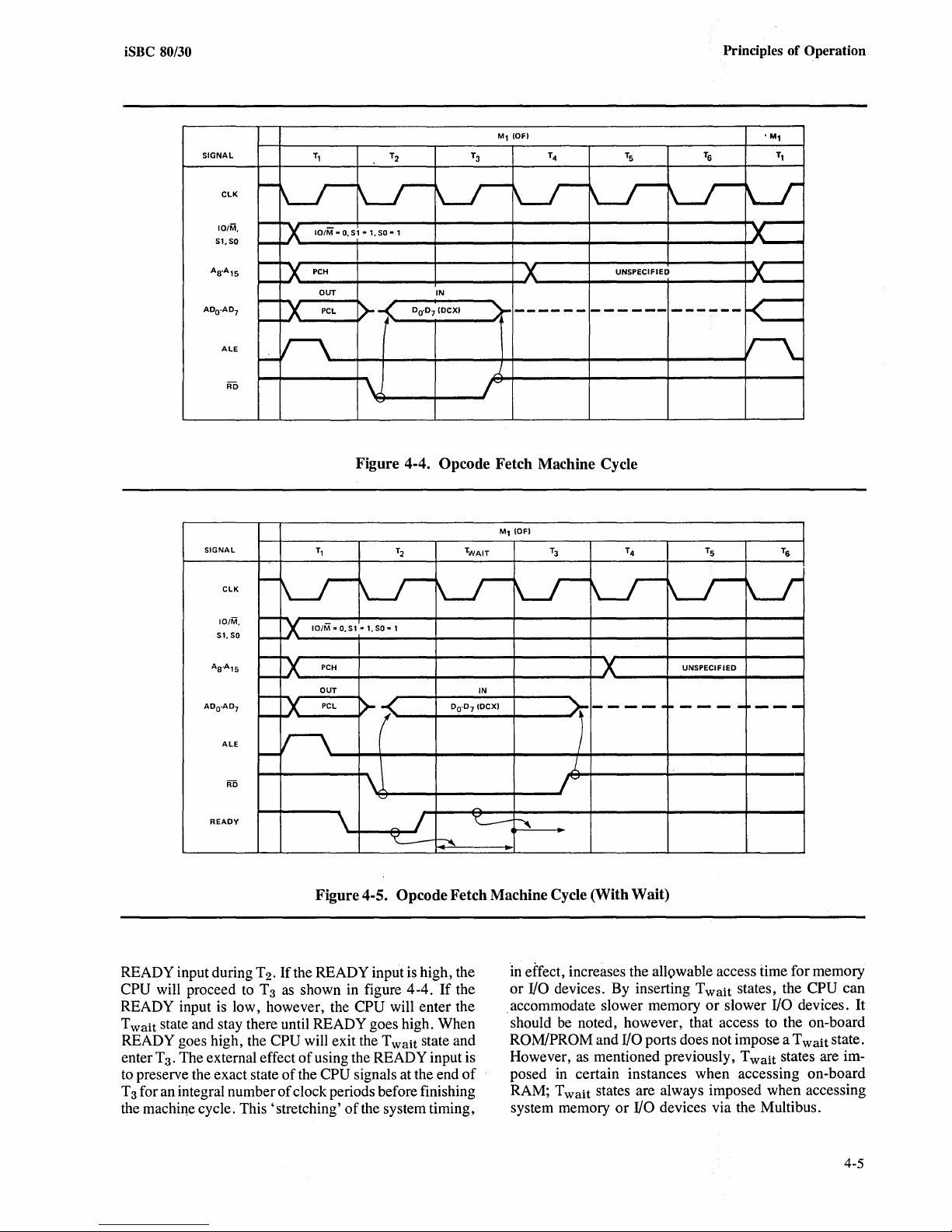
iSBC 80/30
Principles of Operation
SIGNAL
elK
101M,
SI,SO
ALE
Figure 4-4. Opcode Fetch Machine Cycle
SIGNAL
ClK
101M,
SI,
AS-A15
ADO-AD7
ALE
R5
READY
to--
to--
SO
to--
I--
to--
I--
to--
to--
Tl
'-----J
10/M3O,S131,SO-1
)(
PCH
)(
OUT
PCl
D<
r-\
T2
\-.I
~-(
!
--'
~
'L--
TWAIT
\-.I
00-0
N
Figure 4-5. Opcode Fetch Machine Cycle (With Wait)
READY input during T
CPU will proceed to T 3
READY input
is
•
If
the READY input
2
as
shown in figure 4-4.
is
high, the
If
the
low, however, the CPU will enter the
Twait state and stay there until READY goes high. When
READY goes high, the
enterT
.
The external effect
3
to preserve the exact state
T 3 for an integral number
the machine cycle. This 'stretching'
CPU will exit the Twait state and
of
using the READY input is
of
the CPU signals at the end
of
clock periods before finishing
of
the system timing,
of
Ml
(OFI
7
IN
(DCXI
T3
\-.I
~
T4 T5
~
-----
L-I
UNSPECIFIED
~----
LJ
10---
)
1
,'-'
~
-c:::::=
~
in effect, increases the allowable access time for memory
VO
devices. By inserting Twait states, the CPU can
or
_ accommodate slower memory
be
should
ROM/PROM and
However,
posed
noted, however, that access to the on-board
VO
ports does not impose a Twait state.
as
mentioned previously, Twait states are im-
in
certain instances when accessing on-board
or
slower
VO
RAM; Twait states are always imposed when accessing
system memory
or
VO
devices via the Multibus.
TS
devices. It
4-5
Page 71

Principles of Operation
iSBC 80/30
4-20. MEMORY READ TIMING. Figure
of
the timing
cles, the first without a Twait state and the second with
one Twait state. Disregarding the states
lines, the timing during T 1 through T 3
opcode fetch machine cycle shown in figure
major difference between the opcode fetch and memory
read cycles is that an opcode fetch machine cycle requires
four
or
cycle requires only three T -states.
between the two cycles is that the memory address used
for the opcode fetch cycle
program counter
tion; the address used for a memory
of
several origins. Also, the data read from memory
placed into the appropriate register istead
tion register. Note that a T wait state is not imposed during
a read
4-21. I/O READ TIMING. Figure
the timing
first without a Twait state and the second with one Twait
state. With the exception
timing
identical. For an I/O read, IO/M is driven high to identify
the
that
One other minor exception
two successive memory read machine cy-
is
six T -states whereas the memory read machine
One minor difference
is
always the contents
(PC), which points to the current instruc-
read cycle can be one
of
on-board ROM/PROM.
4-6
of
two successive I/O read machine cycles, the
of
the IO/M status signal, the
of
a memory read cycle and an I/O read
current machine cycle
is
referencing an I/O port.
is
that the address used for an
4-6
shows
of
the
SO
and
SI
identical with the
4-4. The
of
the
is
of
the instruc-
also illustrates
cycl~
is
I/O read cycle is 'derived from the second byte
instruction; this address is
A8-A15 and
port is always placed in the accumulator specified by the
IN instruction. Note that a T wait
access
during the access
4-22.
shows the timing
machine cycles, the first without a T
disregarding the states
during T
memory read, and
however, at the end
cycle the
at the beginning
In a memory write cycle, the
disabled and the data to be written into memory is placed
on these lines at the beginning
is driven low at this time to enable the addressed memory
device. During
if
mine
low, Twait states are inserted until READY goes high.
During T
addressed memory device and terminate the
write operation. Note that the contents on the address and
data lines do not change until the next T
ADO-AD7lines. The data read from the I/O
of
on-board I/O devices; T wait states are imposed
of
system I/O devices via the Multibus.
MEMORY
1 is identical to the timing
ADO-AD7 lines are disabled (high impedance)
a Twait state
the
,
3
WRITE
of
I/O read cycles. The difference occurs,
of
T
of
T 2
in
T2
the READY input
is
WR!
line is driven high to disable the
dupilcated onto both the
is
not imposed during the
TIMING.
two successive memory write
wait, state. Again,
of
the
SO
and
SI
lines" the timing
of
an opcode fetch,
1.
For instance,
anticipation
ADO-AD7 lines are not
ofT
required.
in
of
the returned data.
2.
The Write (WRI) line
is
checked to deter-
If
the READY input is
of
an IN
Figure
a memory read
4-7
memory
1 state.
SIGNAL
elK
101M,
SI.S0
A8"A'5
AOo·A07
ALE
iffi
REAOY
~
U-
~
~
I"-
~
~
I"-
......
~
Y.
l""'-
1\
~
MR
T,
10/M·0
OUT
AO-A7
MR
OR lOR
T2 T3
U-
(MRI OR 1 (lORI. s, • 1.
~<
t
'C
U-
°0·°7
-~
T,
U-
SO·
0
IN
)-
LI
10/M·0
OUT
Ao-A7
~(-<
)
1\
1.
r-
~
""
T2
(MRI
OR 1 (lORI.
,..,
"<----
OR lOR
TWA
u-
SI • '.
°0·°7
~
Figure 4-6. Memory Read (or I/O Read) Machine Cycles
IT
IN
......
'L--
SO·
LI
0
~
T3
)
f-
~
)
)
-<
V-
~
4-6
Page 72

iSBC 80/30
Principles of Operation
4-23. I/O WRITE TIMING. Figure 4-7 also illustrates
of
the timing
first without a T
state. With the exception
timing
identical.
4-24.
two successive
wait
of
a memory write cycle and an
INTERRUPT
ING. Figure 2-8 shows the CPU timing in response
INTR input being driven high by PIC
CPU interrupt enable flip-flop has been set by a previously executed Enable Interrupt instruction). The status
of
the TRAP, RST
inputs are sampled during CLK
mediately preceding T 1
interrupt, the
enters the Interrupt Acknowledge (INA) machine cycle.
With two exceptions, the INA machine cycle is identical
with the
exception
opcode fetched will be from an
exception
though the contents
the address lines, the address lines are ignored.
When INTA
tion which causes the
Opcode Fetch (OF) machine cycle. The first
is
is
is
7.5,
CPU clears its interrupt enable flip-flop and
that 101M = 1, which signifies that the
that INT A
of
asserted, the PIC provides a CALL instruc-
VO
write machine cycles, the
state and the second with one T
of
the 101M status signal, the
VO
cycle are
ACKNOWLEDGE
A30 (assuming the
RST 6.5, RST
of
M
1.
If
INTR was the only valid
VO
is
asserted instead
CPU program counter
CPU
to
push the contents
5.5,
of
the T -state
device. The second
TIM-
and INTR
of
RD. Al-
is
sent out on
of
wait
to
im-.
the
the
program counter onto the stack before jumping to a new
location. After receiving the CALL opcode, the
perform a second INA machine cycle (M2)
byte
of
second
timing
of
T-states.
the CALL instruction. When all three bytes have been
received, the
inhibits the incrementing
the three INA cycles so that the correct program counter
value can be pushed onto the stack during
During
(MW) machine cycles to write (push) the contents
program counter onto the top
places the two bytes accessed during
upper and lower bytes
the same effect as jumping the execution
the location specified by the CALL instruction.
After the interrupt service routine
pops the stack and loads it into the program counter, and
resumes system operation at the point
is
the programmer's responsibility to ensure that the interrupt enable flip-flop
vice routine.)
the CALL instruction from the PIC. The
M2
is
identical with M 1 except that
M2
is
followed
CPU executes the instruction. The CPU
M4
and M
by
M3
to access the third byte
of
the program counter during
,
the CPU performs Memory Write
5
of
the stack. The CPU then
of
the program counter. This has
is
is
set before returning from the ser-
to
M2
M4
M2
and
of
the program to
executed, the CPU
of
the interrupt. (It
CPU
access the
has three
and M
of
M3
into the
of
5
the
.
SIGNAL
S1,SO
AIfA
AOO·A0
READY
elK
101M,
'5
ALE
WR
T2
(MWI
MWOR lOW
TWA
l.....r-
OR 1 (lOWI,
SI " 0,
°0·°7
IT
LJ
sq
a 1
T3
'-
)
)
)
V-
~
MWOR lOW
T,
-
LI
-
i-
ex
~
D<
~
~
7
ex
~
V\
~
101M
OUT OUT
AO-A7
~
- 0
(MWI
T2 T3
L.t
OR 1 (lOWI,
00.0
SI
"0,
7
SO·
1
T,
LI
:
LI
IO/M·O
OUT OUT
AO·A7
v---\
r
~
'L
..
""'"
L-
~
Figure 4-7. Memory Write (or
~
1/0
Write) Machine Cycles
4-7
Page 73

Principles of Operation
iSBC 80/30
SIGNAL
ClK
INTR
INTA
IO/M,SI,SO
AS·A
AOO·A0
ALE
I5
7
Ro
Wii
M2(MRI
T2
u.~
~
1
(0,1,01
(PC·l1H
IN
00.0
7
T3
U-
~
X
~
}
IE
n
I
Tl
V V
---
f
><
Tl
OUT
M2 (lNAI
T2
U-
1\
(1,1,11
PCH
00.07 (821 }
)-,
T3
Lr
-
r
IN
Ml (lNAI
T3
T4
T5
T2
TWA
IT
u-
IF
IF
T6
U-
V
-
I
PCH
00.[)7
IN
(CALLI
(1,1,11
}
~
---
---
---
OC
~
€
r\
SIGNAL
ClK
INTR
INTA
IOIM,SI,
AS·A,5
AOO·A0
ALE
--
RO
WR
T,
\J
1---
M3(1NAI
T2
V
-
T3
lr
T,
Lr
MA(M~')
T2
u-'
T3
V
MS
(MW)
T,
T2
V V
T3
V V V
Ml
(OF)
T,
T2
TWAIT
V
1\
OUT
(0,0,1)
(SP·2)H
OUT
00'~7
lX
IX
(PCL)
~
f\
so
tx
[X
7
E
f\
OUT
(1,1,1)
PCH
x
DO,
IN
7 (B3) }
X
X
OUT
-E
1\
(0,0,11
(SP·l)H
X
X
OUT
00.07 (PCH)
E
If\.
OUT
(0,1,1)
PCH(B3)
)-{,
IN
0
.0
7
0
NOTE: DISREGARD TWAIT STATES; NO TWAIT STATES IMPOSED ON 80/30 APPLICATION OF INTA,
Figure 4-8.
4-8
Interrupt
Acknowledge' Machine Cycles
Page 74

iSBC 80/30
Principles of Operation
4-25. ADDRESS BUS
The address bus
and 4-2. The lower eight bits
address or
reference machine cycle or an I/O reference machine
cycle
is
in progress) are output by the CPU during the first
clock cycle (T
source
to
third cycles (T
Latch Enable (ALE) signal issued by the
strobes these eight address bits into Latch
The lower eight address bits
placed on the
high-order address bits (AB8-AB 15). These address bits
are decoded by the following:
a. AB2-AB7 to
b.
ABA-ABF
(sheet 3).
ABO-ABB
c.
d.
ABD-ABF to On-Board RAM Decoder A17 (3ZD7).
4-26.
BUS
Bus Time Out one-shot A38 (lZC7)
leading edge
CPU during T 1
halted, or
mately
BTMO signal on pin
jumper 115-116 is installed, the
(A38 pin 6) drives the
gates A39 and A28 and allows the
state.
The
jumper matrix post 122 (7ZC3).
RST
hang-up state, the rising edge
cause
10
BUS TIME OUT/ signal is also applied
7.5 input and A38
an
is
shown in weighted lines
(ADO-AD7)
I/O address (depending on whether a memory ,
1). The CPU ADO-AD7 pins become the
or input from the data bus during the second and
2 and T
3).
The trailing edge
(ABO-AB7) from A23 are
iSBC 80/30 address bus together with the
I/O Address Decoder A50 (6ZA 7).
to
PROM
to PROM A25/A37 (3ZA3).
Address
in
figures 4-1
of
the memory
of
the Address
CPU during T 1
A23
(2ZD3).
Decode
Logic
TIME OUT
is
retriggered
of
the ALE signal, which
of
every machine cycle. If the CPU
if
the CPU
milliseconds, A38 times out and asserts the
interrupt to report this event.
is
hung up
34
CPU READY line high through
in
of
the auxiliary bus (P2). If
is
retriggered following a CPU
of
is
asserted
a wait state for approxi-
BUS TIME OUT/ signal
CPU to exit the wait
If
jumpered
BUS TIME OUT/ will
to
interrupt
to
the CPU
by
by
the
the
4-28. READ/WRITE SIGNAL GENERATION
The COMMAND/ signal, which
with the various on-board read/write operations,
erated by A45-3 (2ZB4) when the
is
true. The following paragraphs describe how the
various
4-29.
nals (2ZC2) are derived simply by gating the status
CPU 10/M, RD/, and
ADR signal
WRT/ signal
status.
4-30.
ADR, MEMRD/, and MEMWR! signals (2ZB2, 2ZC2)
are also derived simply by gating the status
10/M, RD/, and
signal
MEMWR! signal is the logical AND
inverted
TheADV
by multiplexing the
table 4-1. During all memory references, the CPU
status pin is low and activates the gate input to 8:4 Multiplexer A35. The select pin
pin status; when
is
when
For a memory read operation,
logic 1 appears on A35 pin 12. The trailing edge
CPU ALE signal clocks Quad
A34 pin
For a memory write operation,
logic 1 appears on A35 pin 7. The trailing edge
clocks A34 and A34 pin
signal.
For a memory fetch operation,
since the
the ADV MEM RD/ signal
above for the memory read operation.
I/O and memory control signals are generated.
I/O CONTROL SIGNALS. The I/O control sig-
WR!
is
the buffered IO/M pins status; the I/O
is
the logical AND
MEMORY CONTROL SIGNALS. The MEM
WR!
pins. For example, the MEM ADR
is
the buffered and inverted IO/M pin status; the
IO/M pin status.
MEM RD/ and ADV MEM WRT/ are derived
CPU
SO
SO = 0,
SO
= 1, the
14
asserts the AD V MEM RD/ signal.
S 1 status
the"
"B"
inputs are selected.
11
is
applied to both the 4 A and 4 B inputs,
is
used
CPU RD/ orWR! signal
pins. For example, the I/O
of
the 10/M and
of
and S 1 pin status. Refer
of
A35
is
controlled by the
A"
inputs are selected and,
SO
= 0 and S 1 = 1 and a
"D"
Flip-Flop A34 and
SO
= 1 and
asserts the ADV MEM WRT/
SO
= 1 and
is
generated
in
conjunction
is
WR!
of
the
the
WR!
SI
= 0 and a
of
SI
= 1 and,
as
described
gen-
of
the
pin
CPU.
and
10/M
SO
of
the
ALE
to
4-27. DATA BUS
The CPU ADO-AD7 pins become the source
of
tion
cycles. Data can be sourced to
ing:
a. Data Buffer A24 (4ZC6).
b. Data Buffer A52 (9ZD6).
the data bus
DBO-
DB7 during T 2 and T 3 clock
or
destina-
or
input from the follow-
or
When the read, write,
CPU RD/
(2ZB3)
A?4; the next rising edge
4-31. DUAL
The Dual Port Control logic (figure 5-2 sheet 9) allows the
on-board RAM facilities to be shared by the on-board
, CPU and another bus master via the Multibus. When not
or
WR!
is
clocked and set. The output at A44-6 clears
PORT
fetch operation
pin goes false and Flip-Flop A44
of
ALE clears A44.
CONTROL
is
complete, the
LOGIC
4-9
Page 75

Principles of Operation
iSBC 80/30
acting as a bus master
RAM, the iSBC
or
when not accessing its on-board
80/30 can act
as a "slave"
RAM device
in a multiple bus master system. When accessing its
on-board RAM, the on-board
CPU has priority over any
attempt to access the on-board RAM via the Multibus. In
this situation, the bus access is held off until the
DUAL PORT CTL P·PERIODS
22.12 MHz
ON
BD RAM
RaT
ADV
MEM
RDI
OR
WRTI
SLAVE RAM RaTI
SLAVE RAM
RDI
OR
WRTI
IL
0
0
0
0
____
PO
I
~--
CPU has
P1
P2
I I
, ( I
-
__
----
completed its particular read or write operation. When a
bus access is in progress, the Dual
the'
enters
'slave" mode and any subsequent CPU request
will be held off until the slave mode
4
-9
and 4
-1
0 are timing diagrams for the Dual Port Con-
Port Control Logic
is
terminated. Figures
trollogic.
P3
P4
__
P13
~I~
I P14 I P15 I P16 I P17 I
__
-------------r
FF
A43·15 a
FF A55·9 a
FF A55·8 Q
FF A43·11 Q
FF A43·6 Q
OFF BD
CSI
RAM
RDI
OR
RAM XACKI
RAM AACKI
WRTI
0
0
0
0
0
0
0
0
0
Figure 4-9. Dual Port Control Bus Access Timing With CPU Lockout
611·9
4-10
Page 76
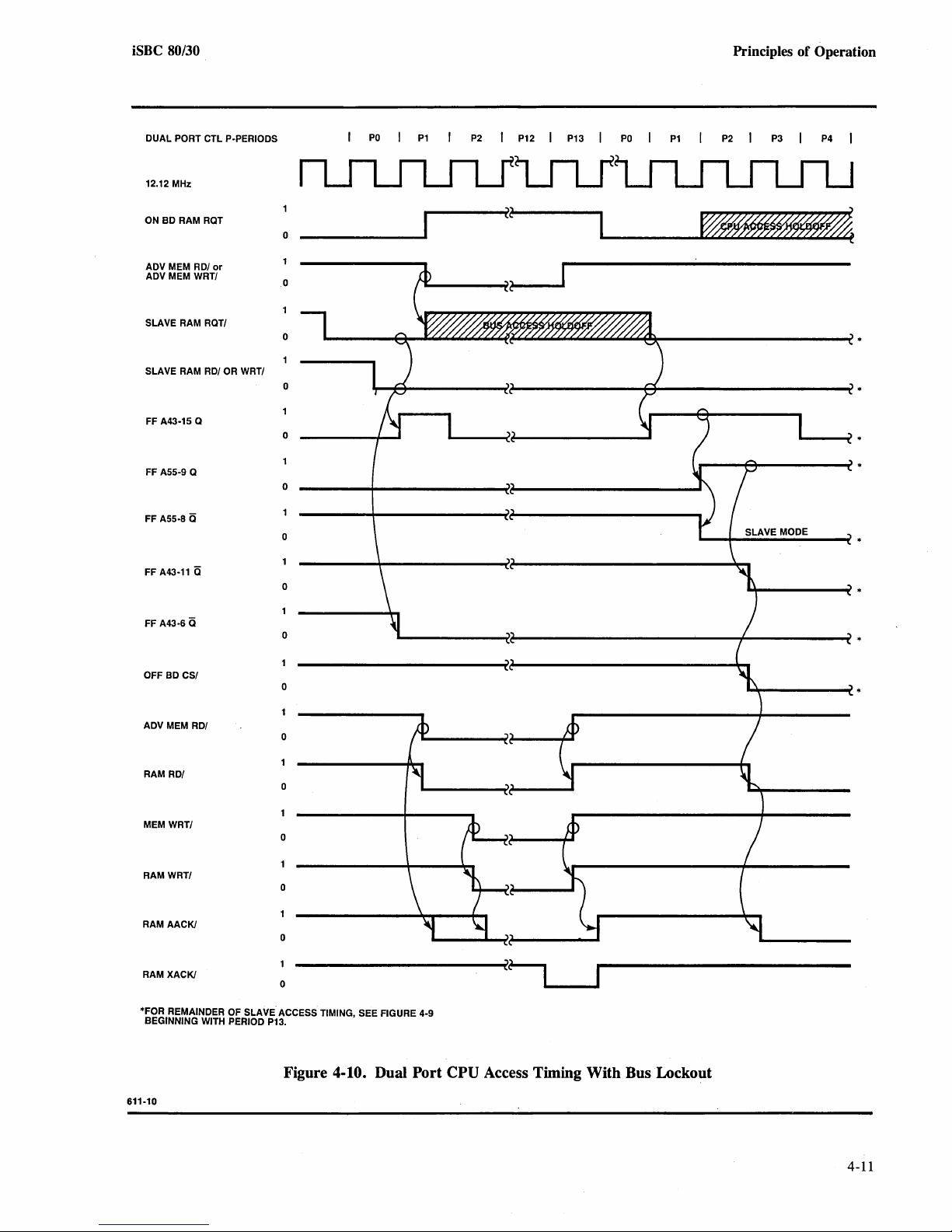
iSBC 80/30
Principles of Operation
DUAL PORT CTL P·PERIODS
12.12 MHz
ON
BD RAM
RaT
ADV
MEM
RDI
MEM
WRTI
or
OR
WRTI
ADV
SLAVE RAM RaTI
SLAVE RAM RDI
FF
A43·15 a
A55·9 a
FF
FF A55·8 Q
FF A43·11 Q
PO
P1
P2
P12
P13
PO
P1
P2
P3
P4
22
o
o
o
o
o
o
o
o
FF A43·6 Q
OFF BD CSI
ADV
MEM
RDI
RAM RDI
MEM
WRTI
RAM WRTI
RAM AACK/
RAM XACK/
*FOR REMAINDER
BEGINNING WITH PERIOD
OF
o
o
o
o
o
o
o
o
SLAVE ACCESS TIMING, SEE FIGURE
P13.
Figure 4-10. Dual
4.9
Port
CPU Access Timing With Bus Lockout
611·10
4-11
Page 77

Principles of Operation
4-32. BUS
Dual
tibus.
scriptive references.) When
SLA VE RAM RD/ or SLAVE RAM WRT/ are true,
A43 -15 goes high and A43 -6 goes low on the next rising
edge
of
is
to synchronize the asynchronous command and the
purpose
from aborting a bus access after A55-9 goes high at the
of
end
At the end
A55-8 asserts the
A55-8 and A43-6 are ANDed to hold A55-9 in the preset
(high) state. At the end
asserts the
input low to RAM Controller A66. The output
also enables pin I
to gate the RAM RD/
Approximately one-half to two clock cycles later, A66
asserts the RAM AACK/ signal and, at the end
A43-15 goes low.
The RAM Controller asserts RAM XACK/ during
and SLA VE XACK/
master then first raises the
RAM WRT/ signal and then the
signal. When
RAM Controller raises RAM AACK/ and RAM XACK/.
At the end
P16, A55-9 goes low and A59-8 goes high. At the end
P17, A43-11 goes high and terminates the OFF BD CS/
signal.
The foregoing discussion pertains only to the operation
the Dual Port Control for bus access
The actual addressing and the transfer
cussed in paragraph 4-42.
4-33.
the Dual
on-board
for descriptive purposes.) To demonstrate that the
has priority in the access
shows that the SLAVE RAM RQT/ and a SLAVE RAM
RD/ or
access
during which time A43-15 has been clocked high and
A43 -6 has been clocked low.
When the
asserted, the AD V MEM RD/ signal is driven through
A60-15 to assert the RAM RD/ signal. The RAM Control-
ler then asserts RAM AACK/, which
A62-8 to produce RAM QAACK/. At the end
A43-15
cess timing cycle. (For a write cycle, the MEM
signal
ACCESS
Port Control timing for RAM access via the Mul-
(P-periods
the clock at the end
of
A43 -6
PI).
of
PI,
OFF BD CS/ signal, which drives the PCS/
SLAVE RAM RD/ or WRT/ goes false, the
of
P15, A43-6 is clocked high. At the end
CPU
ACCESS
Port Control timing for RAM access by the
CPU. (P-periods
SLAVE RAM WRT/ are active when the CPU
is.
initiated. The timing has progressed through
ON BD RAM RQT and ADV MEM RD/ are
is
clocked low to effectively abort the slave ac-
TIMING. Figure
PO
through
is
to prevent a subsequent CPU request
A55-9 goes high and A55-8 goes low;
SLAVE MODE signal. The outputs
of
A60-7, A60-3, A60-5, and A60-9,
in
PI7
SLAVE RAM RQT/ and
of
PO.
(The purpose
of
P2, A43-11 goes low and
or
RAM WRT/ signal to A66.
driven onto the Multibus. The bus
SLAVE RAM RD/ or SLA VE
4-9
illustrates
are used only for de-
of
A43 -15
of
A43
-II
of
P3,
P13
SLAVE RAM RQT/
of
on-board RAM.
of
data are dis-
TIMING. Figure 4-10 illustrates
PO
through P13 are used only
CPU
of
on-board RAM, figure 4-10
PO
is
driven through
of
PI,
WR!
is
used instead
of
ADV MEM WRT/.
of
of
of
of
iSBC 80/30
During
PI2
the RAM controller asserts RAM XACK/ (not
used by the
ON BD RAM go false to complete the CPU access.
and
On the following rising edge
RAM RQT/ and SLAVE RAM RD/
WRT/ signals,
access, set A43-15 once again to initiate the slave access
timing cycle.
The foregoing discussion pertains only to the operation
the Dual Port Control for CPU access
The actual addressing and the transfer
cussed in paragraph 4-41.
CPU) and, during P13, the ADV MEM RD/
of
the clock, the SLAVE
or
SLAVE RAM
which have been held
off
during the CPU
of
on-board RAM.
of
data are dis-
of
4-34. MULTIBUS INTERFACE
The Multibus interface consists
(8ZD5), bidirectional
(8ZA2), bidirectional Data Bus Driver A74/A75 (8ZB2),
and the
sheets 3 and 5).
The Bus Controller allows the
role
and read/write command logic. The falling edge
BCLK/ provides the timing reference, and bus arbitration
begins when the Qualified Command (QCMD/) signal
asserted and the address decoders have determined that
the associated Read
on-board
which
rectly from the
delaying the
(Delaying WT/ ensures the adequate setup
and data to the Bus Drivers before the Write Command
(IORC/ or MWTC/)
The QCMD/ signal activates the Transfer
(XSTR) input to the Bus Controller, which drives BREQ/
low and
master in the system
priority
scribed in paragraph 2-27. The
the Multibus when the
priority scheme
The
BPRN/ input to the Bus Controller
next falling edge
BUSY/ and ADEN/ low. The BUSY/ output indicates that
the bus
will not relinquish control until it raises its
The ADEN/ output, which can be thought
bus
A72/A73 and Data Bus Driver A74/A75. Since the board
is
false (high) and the Address Bus Driver transmit function
is
Slave RAM Address Decode Logic (figure 5-2
of
a bus master and includes bus arbitration, timing,
VO
or
is
used only for Multibus requests,
CPU Write (WT/) signal half a clock cycle.
BPRO/ high. The BREQ/ output from each bus
is
resolved by a parallel priority scheme
iSBC 80/30 gains control
is
in use and that the current bus master in control
control"
not in the slave mode, the QSLA VE RQT/ signal
selected. The steering logic composed
-Address B us Driver A 72/ A 73
or
Write Command is-not intended for
memory. The QCMD/ signal (lZD8),
CPU Read (RD/) signal
is
asserted.
is
used by the Multibus when the bus
bus priority is resolved by a serial
as
described in paragraph 2-26.
of
BCLK), the B
signal,
enables
of
Bus Controller A67
iSBC 80/30 to assume the
of
is
is
derived di-
or
derived by
of
the address
Start Request
as
de-
BPRO/ output
of
the Multibus when the
is
driven low. On the
us
Address Bus
is
used by
Controller drives
BUSY/ signal.
of
as a "master
Driver
of
A39-6,
is
4-12
Page 78

iSBC
80/30
Principles of Operation
AS9-6, A42-6, and A41-8 (8ZB4) decides which function (transmit
This decision
the board
is
receive)
is
based on the mode (master
in
and whether the command is a read
to
select for the Data Bus Driver.
or
slave) that
or
or
write. For the master mode, a Write Command selects the
transmit function (DIEN is driven high); a Read Com-
is
mand selects the receive function (DIEN
BUS Controller examines its
The
10RR,
driven low).
10WR,
MRDR,
and MWTR inputs and drives the appropriate command
line low on the Multibus. After the command is acknowledged (signified by the addressed device driving AACK/
or
XACK/ low), the CPU terminates the appropriate
command and tristates its address lines. This deselects the
Address Bus Drivers and Data Bus Drivers and causes
to
QCMD/
quishes control
BPRO/ low and then raising BUSY/.
and
It should be noted that, after gaining control
tibus, the
go false (high). The Bus Controller relin-
of
the Multibus by driving BREQ/ high
of
the Mul-
iSBC 80/30 can invoke an override condition to
prevent losing control at a critical time. (For instance, it
may be desired to execute several consecutive commands
without having to contend for the bus after each command
is
executed.) Bus override is invoked by executing a SIM
instruction with accumulator bits 6 and 7 = 1, which
causes the
CPU SOD line to drive the Bus Controller
OVRD input high.
4-35. I/O OPERATION
The following paragraphs describe on-board and system
I/O operations. The actual functions performed by
to
specific read and write commands
are described in Chapter 3.
on -board I/O devices
with the COMMAND/ signal (decoded WR
enables Data Buffer A24 (4ZC6). The function
selected by the CPU S 1 output; S 1 = 1 for read operations
and S 1 = 0 for write operations. For example, data is
a
transferred from the
lines when SI =
1.
DIOO-DI07
lines to the DBO-DB7
After the I/O device has been selected by address bits
AB2-AB7,
address bits
4-37.
AB2-AB7 are decoded by
described in paragraph 4-31.
on-board
specific functions for the chip are selected by
ABO-AB!. (Refer to table 3-2.)
SYSTEM
I/O
OPERATION.
I/O Address Decoder
If
the address
I/O device, I/O AACK/ remains false (high)
and, together with QCMD/, activates the Bus Controller
XSTR input. The false SLAVE MODE/ signal from
ASS-9 (9ZC4) in the Dual Port Control logic enables
Address Buffer AS3/ AS4 and, together with the false I/O
AACK/ signal, enables Data Buffer A52.
us
When the B
Controller gains control
described in paragraph
4-29,
of
it drives ADEN/ low to
select Address Bus Driver A72/A73 and Data Bus Driver
A74/A7S. Since the board is not in the slave mode, the
QSLA VE RQT/ signal is false (high) and the Address Bus
Driver transmit function is selected. The transmit
ceive function
line.
If
the operation is a read, S 1 = 1 and the receive
is
function
function
enabled; for a write,
is
enabled. The steering logic composed
Data Buffer
is
selected by the CPU
SI
= 0 and the transmit
of
A39-6, AS8-6, A42-6, and A41-8 (8ZB4) decides which
to
function
is
in the master mode for off-board operations, a write
select for the Data Bus Driver. Since the board
operation selects the transmit function and a read operation selects the receive function.
or
RD),
of
A24
Address
ASO
is
not for an
the Multibus
or
is
bits
as
as
reSI
of
4-36.
ON-BOARD I/O OPERATION. Address bits
AB2-AB7
are applied to I/O Address Decoder
ASO
and
associated input chip enable gates (6Z7 A). Address bits
AB4-AB7
to provide
enabled,
chip select inputs
bits
When anyone
ADR signal from the CPU (buffered 10/M)
through A46-11 to develop
are decoded by
El,
E2, and
ASO
decodes address bits
to
AB2-AB7
7 6 5 4 3 2
1 1
1
1
1
1
1 1
1 1 1 0 1 1 EC-EF
are decoded as follows:
Bits
o 1 1 0
o 1 1 1
100
1
101
0 E8-EB
of
the five outputs
A48-12,
E3
enable inputs to
the appropriate I/O device. Address
Addresses
08-0B
~C-OF
E4-E7
I/O AACK/. The I/O
A6S-6,
AB2-AB4
of
ASO
goes low, the I/O
and A6S-3
ASO;
toprovide
Chip
Select
Signal
8259CS/
8253CS/
8741CS/
8255CS/
8251CS/
is
when
driven
AACK!
signal drives the CPU READY line high and, together
of
After gaining control
the Multibus the B
proceeds with the control tasks for the remainder
us
Controller
of
the
I/O transfer. Refer to paragraph 4-29 for a description
how the Bus Controller terminates bus control.
4-38. ROM/EPROM OPERATION
The two ROM/EPROM chips are installed by the user in
IC sockets
IFFF are reserved exclusively for ROM/EPROM; the
actual occupied memory space depends on the ROM/
EPROM chips as follows:
Address bits ABO-ABB are applied directly to the inputs
of
A2S-A37 and address bits ABA-ABF are applied
A2S/ A37 (3ZA3). Memory addresses 0000-
Chip
Size
1K x 8
2K
x 8
4K
x 8
Chip Addresses
A25
0OOO-03FF
0OOO-07FF
OOOO-OFFF
In
0400-07FF
0800-0FFF
1000-1FFF
A3
to
4-13
the
of
Page 79

Principles of Operation
iSBC 80/30
ROM/EPROM chip select decoders. When address bits
ABA-ABF are true for the address ranges specified
above,
PROM
signal is also asserted during a read operation, the
ENABLE/ and PROM
AACK!
signal
AACK!
is
true; when the MEMRD/
PROM
signals are true. PROM
ENABLE/ turns on Data Buffer A24 (4ZC6), whose
transmit function
AACK!
drives the CPU READY line high via A28-6
(1DZS). The decoded output
EPROM
the
chip in A2S; the decoded output
ROM/EPROM chip in A37. When the chip is enabled,
the contents
transferred to the
is
enabled by CPU S 1 = 1, and PROM
of
A49-8 selects the ROM/
of
A49-6 selects
of
the location specified by ABO-ABB are
CPU via Data Buffer A24.
4-39. RAM OPERATION
As described in paragraph 4-31, the Dual Port Control
logic allows the on-board RAM facilities to be shared by
the on-board
Multibus. The following paragraphs describe briefly the
RAM Controller and the overall operation
RAM is addressed for read/write operation.
RAM
4-40.
inputs
to
ler A66 (3ZDS). The RAM Controller provides a 64 -cycle
RAS/CAS refresh timing cycle
A
77
-A84. Default jumper 110-111 holds the REFRESH
RQT signal false and the RAM Controller operates in the
automatic refresh mode.
read or write request can be delayed if a refresh cycle is in
progress.
REFRESH RQT signal to be controlled by the CPU
READY
mode. In the invisible refresh mode, the RAM Controller
works around memory accesses
ing the
each instruction fetch. Refresh occurs during T
access is greater than the refresh time, the RAM Controller will automatically refresh RAM. Thus, the RAM will
not generate
power.
The RAM Controller, when enabled with a low input to its
PCS/ pin, multiplexes the address to the RAM chips.
Low -order address bits
input pins and
8202 clock cycle after RAM RD/
first
active. High-order address bits A7-A13 are presented at
the RAM input pins and
second clock cycle after the
satisfied.
The RAM Controller then examines its RD/ and WRT/
inputs.
If
output high to provide a Read signal to RAM;
low, the RAM Controller drives its WE/ output high to
provide a write signal to RAM. If RAM RD/
CPU and by another bus master via the
of
how the
CONTROLLER.
the on-board RAM
In the automatic refresh m.ode, a
Option jumper position 110-106 allows
All address and control
is
supplied by RAM Control-
to
dynamic RAM chips
the
line and thereby implement the invisible refresh
by
refreshing RAM dur-
CPU instruction decode clock cycle which follows
4 but,
if
the
CPU wait states but it will consume more
AO-
A6 are presented at the RAM
RAS/
is
driven low at the beginning
or
RAM WRT/
CASt
is
driven low during the
of
the
RAS/ address hold time is
RD/
is
low, the RAM Controller drives its WE/
ifWRT/
is
is
asserted,
Memory Data Buffer A76 is enabled and RAM data is
latched into A 76 when RAM XACK/
driven low.
When the memory cycle begins, the RAM Controller
drives its SACK/ output low;
AACK!
signal. When the cycle
SACK!
is
used
is
complete (i.e., data is
valid), drives its XACK/ output low. The SACK/ and
XACK/ outputs go high when the RD/
or
WRT/ input goes
high.
4-41.
TION.
ON
BOARD
READ/WRITE
When MEM ADR goes true, Address Decoder
A17 (3ZD7) decodes address bits ABD-ABF. The decoded output from A17 goes low and (1) asserts
RAM RQT/
the RAM Controller
to
the Dual Port Control logic and (2) drives
PCS/ input low. The RAM Controller then multiplexers the address to RAM and, depending
on which input command (RAMRD/
true, drives the WE/ output pin high
is
driven high for a read and driven low during a write.)
The SACK/ signal, which
is
asserted at the beginning
or
or
low. (The WE/ pin
the memory cycle, generates the RAM
When RAM AACK/ goes true, the Dual Port Control
logic generates the RAM QAACK! signal, which is qualified
by
being in the master mode. The XACK/ signal,
which is asserted when the data
RAM
XACK!
signal.
When RAM QAACK/ goes true, the
driven high
the
CPU timing has progressed to
to
the CPU to prevent a wait state. By the time
is
valid, generates the
READY input is
T3
of
cycle, the RAM Controller has already asserted
and the data is valid; i.e., the data has been written into
RAM from the data bus or has been read from RAM onto
the data bus. The
the
CPU during on-board RAM access.
4-42.
BUS
another bus master has control
master can address the
XACK!
signal, however, is not used by
READ/WRITE
iSBC 80/30
OPERATION.
of
the multibus, that bus
as
device. Assuming that the bus master has a 20-bit addressing capability,
ADRO/-ADRF/ and ADRIO/-ADR13/ are
placed on the Multibus and then either MWTC/
MRDC/
decoded by A69 (SZC6) and ADRD/ -ADRF/ are decoded
is
by A68 (SZBS). (A description
dress assignment for bus access
is
asserted. Address bits ADRIO/-ADRI3/ are
of
16-bit and 20-bit
of
RAM
paragraphs 2-17 through 2-19.) The decoded output
A69 provides an enable input
of
A68 drives the SLAVE RAM RQT/ signal low to the
to
A68. The decoded output
Dual Port Control logic.
Assuming no
SLAVE MODE/ signal
CPU access
is
of
RAM is in progress, the
driven low and address bits
ADRO/-ADRF/ are transferred through Address Buffers
is
subsequently
as
the RAM
OPERA-
ON BD
RAMWRT/)
AACK!
signal.
the memory
XACK!
When
a slave RAM
is
given in'
is
of
or
ad-
of
4-14
Page 80

iSBC 80/30
Principles of Operation
A72/A73 to the RAM Controller. When the Dual Port
Control logic asserts the
Controller
PCS/ input is enabled and, depending on which
OFF BD CS/ signal, the RAM
command has been asserted (RAMRD/ or RAMWRT/),
drives the WEI input high to RAM.
The RAM Controller generates
SACK! and XACK/
as
previously described. For a bus access, the SACK/ signal
develops
SLA VE AACK/ and
XACK!
develops SLA VE
XACK/. The controlling bus master then drives the
MRDC/ or MWTC/ command hIgh and deactivates address drivers A 72/ A 73.
4-43. INTERRUPT OPERATION
All interrupts except INTR are connected to the CPU by
jumper connections. (Refer to paragraph 2-20.)
interrupt handling is handled by the internal CPU timing
described in paragraph
4-24,
no further explanation is
considered necessary.
Since
4-15/4-16
Page 81

Page 82

q
611-13
DENOTES
FIGURE
5-2
SHEET NUMBER
5.53 MHZ
Xl
~
SOD
10iM
RD
WR
A8-A15
S085A
CPU
A36
ALE
ADO-AD7
READY
S1
R/W
,6
CONTROL
,
12
ill
I
ABS-ABF
S
,
LATCH
ABO-AB7
DBO-DB7
,8
A23
...
16
I
12
~
Ir
,S
S
,
~
,
[
"-
-
1 = READ
0=
WRITE
,
PROM
AACK
MEM
RD
ABA-ABF
,6
r
t
,
ROMIPROM
ADDRESS
DECODE
LOGIC
Ia
-
PROM ENABLE
L
,
T/R DATA
CS
I'~_v
I_I
/
'6-;....~j,':;
t
~
DATA BUFFER
.ABO-ABB
A24
"13
r;
I r
~
CE
ADDR
PROM A25/A37
li
0100-0107
I
iSBC
80/30
Principles
of
Operation
OVRD
DCBRO'
!"""-"
~4
BPROI
,
BUS OVERRIDE
BUSYI
BUS
BPRN/----+<:
CTRLR
BREOI
A67
10RCI
10WCI
RESET-+
~4
MRDCI
.-
I SYST RAM REO
BCLKI---+-cl
MWTC/
.-L)
f
"'
XSTR
AD~
BUS CTL/
.I
CS
Is
OCMD/
,2
t
I
READ/WRITE
----.
STEERING
READ/WRITE
(f)
LOGIC
::J
III
11
6
!:i
,
Is
::J
==
XACK/
SLAVE MODE/
~
T/R
ADDRESS
..J:-'
ABO-ABF
ADDRESS
AMO-AMF
BUS
R..-
.I
BUFFER
'"
DRIVER
,
16
ADRO/-ADRFI
'16
~
A53/A54
,-
-.,
A721A73
,.
GATE
19
,16
CS
Is
f
Q
ADRD/-ADRF/
,
SLAVE MODEl
SLAVE MODEl BUS
CTL/
3
ON
BOARD
CLK
22.12
MHZ
SLAVE
I
RAM
DUAL
RAM
,3
ONBD
PORT
,7
,4
ADR10/-ADR13/
ADDRESS
RAM ROT
CONTROL
SLAVE
RAM ROT
ADDRESS
AB6-ABF
DECODER
LOGIC
DECODERS
-,
,
~
A17
A6S/A69
(3
[9
Is
-,
Ir
1
t t
ADRS
R/W
PCS
RAM XACKI
22.12
MHZ
ClK
RAM RAM AACKI
CONTROLLER A66
-
-
MEMORY PROTI
3
't
ADDRESS
CONTROL
)(
::J
""
3
-
16K RAM
AUX PWR
A77-A84
-1:
IN OUT
BUS
CTL/
~
f
DR
MO-DRM7
U
~<"t\.,""
~)
READ/WRITE
MEMORY
DATA
BUFFER
-
A76
l~~
J.
1
I3l
cs
:~
cs
R..-
R.~\w\
IB0S
0=---..
Q
DATA
1=~
DATA BUFFER
~
...
..
BUS
DATO/-DAT7/
A52
~
DMO-DM7
~
DRIVER
~
DBO-DB7
A74/A75
[9
Is
Figure 4-2. iSBC 80/30
PROM
and
Dual Port RAM Block Diagram
4-19/4-20
Page 83

CHAPTER 5
SERVICE INFORMATION
5-1. INTRODUCTION
This chapter provides a list
diagrams, and service and repair assistance instructions
for the iSBC
5~.
Table 5
80/30 Single Board Computer.
REPLACEABLE
-1
provides a list
80/30. Table 5-2 identifies and locates the manufacturers
specified in the MFR
parts that are available on the open market are listed in the
MFR
CODE column
made to procure these parts from a local (commercial)
distributor.
of
replaceable parts, service
PARTS
of
replaceable parts for the iSBC
CODE column in table 5 -1. Intel
as
"COML";
every effort should
be
5-3. SERVICE DIAGRAMS
The iSBC 80/30 parts location diagram and schematic
diagram are provided in figures 5-1 and 5-2, respectively.
On the schematic diagram, a signal mnemonic that ends
with a slash (e.g.,
signal mnemonic without a slash (e.g.,
10WC/)
is
active low. Conversely, a
BTMO)
is
active
high.
5-4. SERVICE AND REPAIR
ASSISTANCE
United States customers can obtain service and repair
assistance froin Intel
Support Center in Santa Clara, California, at one
following numbers:
by
contacting the MCD Technical
of
the
Telephone:
or
From Alaska
Hawaii call -
(408) 987 -8080
From locations within California call toll free -
(800) 672-3507
From all other
U.S. locations call toll free -
(800) 538-8014
TWX:
910-338-0026
TELEX: 34-6372
Always contact the MCD Technical Support Center
fore returning a product to Intel for service
will be given a
"Repair
Authorization Number", ship-
or
repair . You
be-
ping instructions, and other important information which
will help Intel provide you with fast, efficient service.
the product
is
being returned because
of
damage sustained
during shipment from Intel, or if the product
warranty, a purc.hase order
is
necessary in order for the
If
is
out
of
MCD Technical Support Center to initiate the repair.
In preparing the product for shipment to the MCD Technical Support Center, use the original factory packaging
material,
if
available.
If
the original packaging is not
available, wrap the product in a cushioning material such
as Air Cap
Sealed Air Corporation, Hawthorne,
TH-240 (or equivalent) manufactured by the
N.J.,
and enclose in
a heavy-duty corrugated shipping carton. Seal the carton
securely, mark it
"FRAGILE"
to ensure careful handling, and ship it to the address specified by MCD Technical Support Center personnel.
NOTE
Customers outside
tact their sales source (Intel Sales Office
thorized Intel Distributor) for directions on obtaining service or repair assistance.
of
the United States should con-
or
Au-
Reference Designation
A1,2,74,75
A3-11
A12
A13,57
A14
A15,16
A17,50
A18
A19
A21
A22
A23
52,
72,
A24,
A26
A27,32
73
Table 5-1. Replaceable Parts
Description
IC,
8226, Bidirectional Data Buffer
IC,
7400, Quad 2-lnput Positive NAND
IC, 74163, Synchronous 4-Bit Counter
IC, 8224, System Clock Generator 8224
IC,
1488, Quad Line Driver
IC,
1489, Quad Line Driver
IC,
74LS138, 3-to-8 Decoder/IMultiplexer
IC,
74LS11, Triple 3-lnput 'Positive NAND
IC,
8255A, Programmable Peripheral Interface 8255A
IC,
8253, Programmable Interval Timer 8253
IC, 8251A, Serial
IC,
74LS373, Octal D-Type Latches
IC,
DP8304, Bidirectional Data Buffer
IC,
74S03, Quad 2-lnput Positive NAND
IC,
74LS32, Quad 2-lnput OR SN74LS32
1/0
Interface (USART) 8251A
Mfr. Part No.
8266
SN7400
SN74163
LM1488
LM1489
SN74LS138
SN74LS11
SN74LS373
DP8304
SN74S03
Mfr.
Code
COML 4
TI
TI 1
COML
NAT
NAT
TI 2
TI
COML 1
COML
COML 1
TI 1
COML 4
TI
TI
Qty.
9
2
1
2
1
1
1
2
5-1
Page 84

Service Information
iSBC 80/30
Table 5-1. Replaceable Parts (Continued)
Reference Designation
A28
A29
A30
A31
A33,40,51 ,63
A34,43
A35
A36
A38
A39,45
A41
A42,62
A44,55
A46,58,61 ,64
A47
A48
A49
A53,54
A56
A59
A60
A65
A66
A67
A68,69
A70,71
A76
A77~4
C1-6,
19,21,29,30,31,32
36-44,46,48,50-53,
55,60-63
C7
C8,49
C9,10,22-28,33,35,45,
47,54,56,58,59,64-72,
79,81,83,85,87,89,
91,94
C57
C73-77,93
C78,82,86,90
C80,84,88,92
C95
CR1
Q1
Description Mfr. Part No.
IC,
74S20, Oual Positive NANO
JC,
Z438, Quad 2-lnput Positive NANO SN7438
IC,.
8259A, Prowammable . Interrupt Controller
IC,
74LS74, Oual OoType Flip-Flops
IC,
74S04, Hex Inverters
IC,
74S175, Quad
IC, 74LS157, Oata Selector/Multiplexer SN74LS157
IC,
8085A Central Processor Unit
IC, 9602, One-Shot Multivibrator
IC,
74LS08, Quad 2-lnput Positive ANO
IC,
74S08, Quad 2-lnput Positive ANO
IC,
74S32, Quad 2-lnput OR
IC,
74S74, Oual
IC,
74S00, Quad 2-lnput Positive NANO SN74S00
IC,
74S11, Triple 3-lnput Positive NANO SN74S11
IC, 74LS27, Triple 3-lnput Positive NOR
IC,
74S10, Triple 3-lnput Positive NANO SN74S10
IC,
74LS240, Octal Buffer/Line Oriver SN74LS240
IC,
74S140, Oual 4-lnput Positive NANO SN74LS140
IC,
74LS02, Quad 2-lnput Positive NOR SN74LS02
IC,
8097, Three-State Oata Buffer
IC,
74LSOO,
IC, 8202, RAM Controller
IC,
Bus Controller OBO
IC,
3205, 1-of-8 Binary Oecoder
IC,
74LS04, Hex Inverters SN74LS04
IC, 74S373, Octal OoType Latches SN74S373
IC,
2117, Random Access Memory 2117
Capacitor, Ceramic,
CapaCitor, tant,
CapaCitor, mono,
CapaCitor, mono,
CapaCitor, mono,
CapaCitor, tant,
CapaCitor, mono,
CapaCitor, mono,
CapaCitor, mono,
Oiode,1N4002
Transistor, 2N3904 2N3904
OoType
Flip-Flops
OoType
Flip-Flops
Quad 2-lnput Positive NANO
0.01/-LF,
25V,
+80%,
-20%
10/-LF,
20V, 10%
10pF, 500V, 5% OBO
0.1/-LF,
50V,
+80%,
-20%
220pF, 500V, 5%
22/-LF,
15V, 10% OBO
1.0/-LF,
50V, 10%
0.01/-LF,
33/-LF,
50V,
50V
+80%,
-20%
SN74S20
8259A
SN74LS74
SN74S04
SN74S175
8085A
9602
SN74LS08
SN74S08
SN74S32
SN74S74
SN74LS27
8097
SN74LSOO
8202
3205
OBO
OBO
OBO
OBO
OBO
OBD
OBO
1N4002
Mfr.
Code
TI
TI
COML
TI
TI
TI
TI
COML
NAT
TI
TI
TI
TI
TI
TI
TI
TI
TI
TI
TI
COML
TI
COML
INTEL
COML
TI
TI
COML
COML
COML
COML
COML
COML
COML
COML
COML
COML
TI
TI
Qty.
1
1
1
1
4
2
1
1
1
2
1
2
2
4
1
1
1
2
1
1
1
1
1
1
2
2
1
8
32
1
1
35
1
6
4
4
1
1
1
R1
,3-5,10,11,14,17-20,
23,25-29,32,33
R2
R6~,
15, 16,30,34,35
R9,12,13
R13
R21
R22
R24
R31
RP1,2
XA1,2
XA3-11
XA20,36,66
XA25,37
Y1
Y2
Resistor, comp, 1 K ohm,
Resistor, comp,
Resistor, comp,
Resistor, comp,
Resistor, comp, 5.1K ohm,
Resistor, comp, 330K ohm,
Resistor, comp, 33K ohm,
Resistor, comp,
Resistor, comp, 2.2K ohm,
Resistor, package, 1 K ohm,
Socket, IC, 16-pin C-93-16-02
Socket,
Socket, IC, 40-pin 540-A3670
Socket,
Crystal, 22.1184-MHz HW3
Crystal, 18.432-MHz MP184
Post, Wire Wrap 85931-6
Extractor, Card
5-2
1f4W
5% OBO
100K ohm,
10K ohm,
620K ohm,
270K ohm,
IC,
14-pin C-93-14-02
IC,
24-pin
1f4W
5%
1f4W
5%
1f4W
5%
V4W
5% OBO
1f4W
5% OBO
V4W
5% OBO
1f4W
5% OBO
1f4W
5%
10-pin OBO
OBO
OBO
OBO
OBO
C-93-24-02
S-203
COML
COML
COML
COML
COML
COML
COML
COML
COML
COML
TI
TI
AUG
TI
CTS
CTS
AMP 192
SCA
19
1
8
3
1
1
1
1
1
2
2
9
1
2
1
1
2
Page 85

iSBC 80/30
Service Information
MFR. CODE
AMP
AUG
CTS
MANUFACTURER
AMP,
Inc.
Augat,
Inc.
CTS Corp.
Table 5-2. List
ADDRESS
Harrisburg, PA
Attleboro, MA
Elkhart,
IN
of
Manufacturers' Codes
MFR. CODE MANUFACTURER
NAT
SCA Scanbe,
TI Texas Instruments
OBD Order by Description; available from any
National
Semiconductor
Inc.
commercial source
ADDRESS
Santa Clara, CA
EI
Monte, CA
TX
Dallas,
5-3/5-4
Page 86

Page 87

o
c
B
A
~
192.
PLACES
~~G
olJiJ
L,--=--"'---
8.
DIIJIEN510I-JS
ARE
lhl
It\CJ1ES.
7
86 2 PLACES
(AI,2)
6
GJ
MARie
VENDOR I.D.
VI
ITH
CONTI?ASTING
PtRM
COLOR,APf?OX
Wl1fRr
SWONfJ.
GJ
5.
tB
3.
2.
".:11
T~RU
CIS
NOT
TO
BE
INSTALLED
AT
THIS
LEVEL.
WIRE
PER
WIRE "ROUTiNG
LIST"
.~)He:ET
(,
AIJD
7
OF
PART:; LIS
T.
USING
ITEM
"J.INSULATE
UNDER ITEM
71,72.
2PLAt:.ES.('1'I,V2).
MARK
DASH
"'0.
AND
REV.
LEVEL
WITH
C.ONTRASTINcS
,PERM
.COLOR,
.12.
HIt;H,
WHERE
5/-10WN.
WORKMANSHIP
PER MCD o..AW
007.
I.
ASSEMBLY
PART
NO.
IS
IOOI57b-XX.
PWA
AND
P/L
ARE
TRACKING
DOCUMENTS
}JOTES:
UNLESS
OTHERWiSe-
SPECIFIED.
8
7
6
85
9
PLACES
(A3-1/J
CvM
f00NEN7
SIDE
5
iSBC 80/30
4
4
3
Service Information
2
REVISIONS
LTR
DESCRIPTION
PROTOTYPE
? ENG R
RELEASE
3
ENGR
REL
ECo"
IB21
2
PLACES
lA25,
371
o 0
10
.60
o
L!------l..
·L.so
1
SIGNATURE
AND
DATE
OFT
CHK
ENGR
SCALE:
NON'E
II'lSULATINGTAFJ;:
FOr-.
VI
ANt:.
v2
SEE
SEPARATE
PARTS
LIST
DESCRIPTION
D
c
B
r-
______
~------~---Q~U-AN-TI-TY-P-ER-D-A-SH-N-O-.--~------------~--
__
~~~~~----------------~A
SCALE:
TOL.
ANGLE
±
FINISH:
3
SIGNATURE
DRN
BY
A.
SHARNEE
CHK
fif
.
OFT
APPD
AUTH
BY
CODE:
SHEET
2
DRAWING
NO.
3055
BOWERS
AVE.
SANTA
CLARA
CALIF. 95051
EIOOl576
1
REV
4.
Figure 5-1. iSBC 80/30
Parts
Location Diagram
5-5/5-6
Page 88
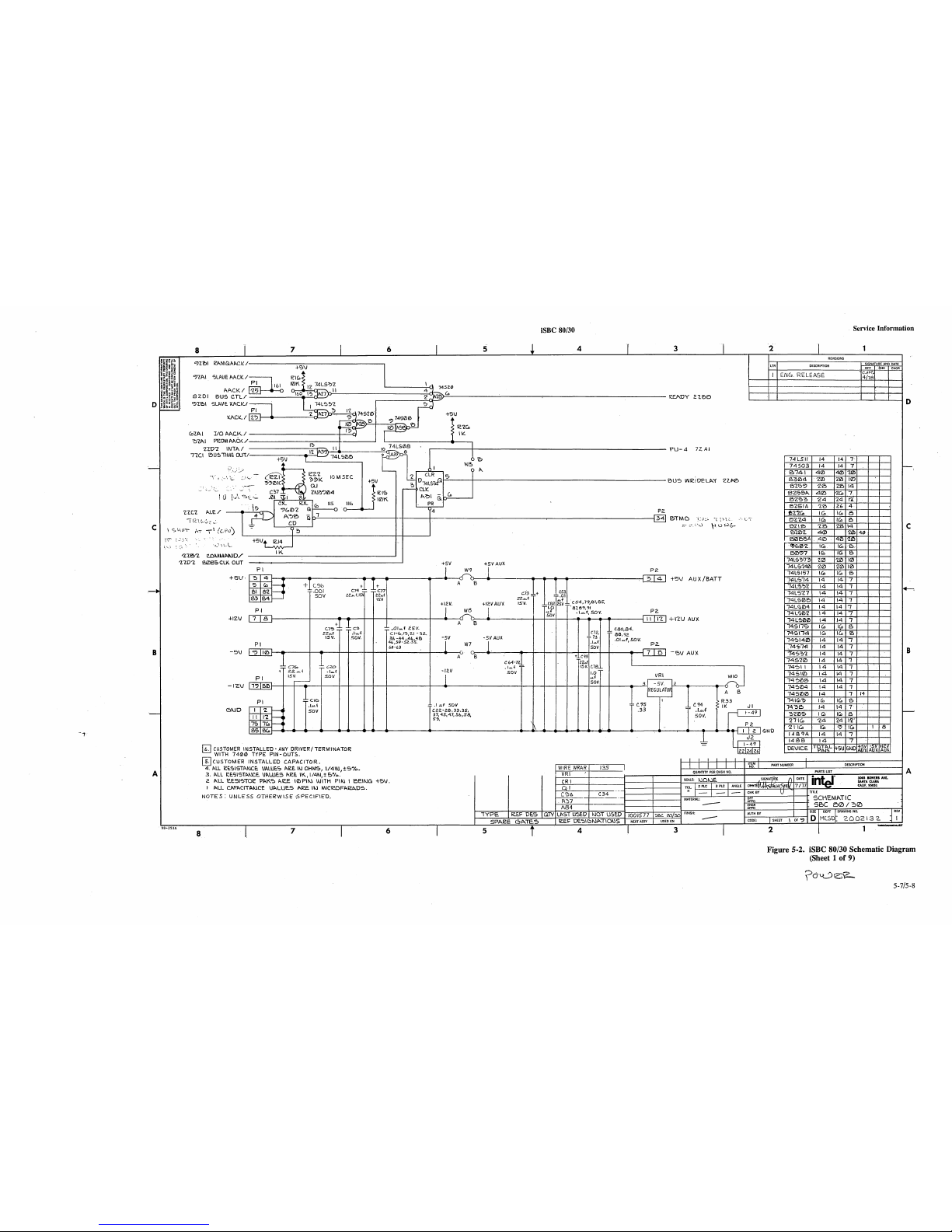
Page 89

o
c
B
A
8
THIS
ORAWIJroIG
CONTAINS
INFORMATION
WHICH
IS THE
'AQfflIETARY
!'"orERTY
OF
INTEL
CORPORATION.
THIS
DRAWING
IS
RECEIVED
IN
CONFIDENCE
AND
In
CONTENTS
MAY
NOT ,e DISCLOSED WITH-
OUT
THE
''''OR
WRITTEN
OONSENT
OF
INTEL
COR~RATION
INIT
/
I'"
1,\
7
LAI
~f:~ET
OUT
"O~'i..<Z-
7
~
+5\1
~7
10K
R.Co
I~I<
R.B
I~K.
74S(l)4
PI
I
'2.
14
i0~
A~\-z-e-
11
74M,R,~7"
17.
I~
0<"
Q.c:=sex-
P2
PFSI
fOl.A) ... ~ .;::"'\
....
17
~~~
lI.e?:>
{
77el
I~T~
-'1C.1
1l.JT~
7S
?Lei
INTR.c".,?
77C I I
lilT
I<.
'?I':)
T"Z.DI
T~P
,,_I
"Z.D~
I<.E!\VY
.~
I,')
,'
...
:
-'/"-
X.
~,c:...\;:...
1
-;J"\--.;.'-,
E)U5
W~
VElAY
8
(f'
\ c..)
....
,
-.
7
1(»9
0-
I~B
IGJ1
14504
!1
4
-;::"":J~
14-:'04
I
'l
....
P\':ll
6
rb~7
It\.ITt>.
II
...
I
~l
CLKOUT
?:Jl'
=00
4
C
'26
A~F
A.I!:)
'L7
f\BE
P
1\14
1\1~
'lIn
t>.~D
7.':>
p.ec.
U
Pd7.
'24
AB~
Pd
I
PlII-'l
27
A.'bPl
Plq
Z'l
"'be:?
'll
A'b~
~
~E.SE.T
1"-1
A6
ADell
I'Z
Ve,(/)
A.Dl
l~
DBI
14
DEl'l
AD'Z
p..o~
1'3
DE5~
A.D4
ICo
De,
4
17
DB'!l
;"'D'S
15
D~CD
P-..OCO
A.D7
It:?)
DBl
Q
~ESETOUl
~
\-\lDA.
A.LE.
~(l)
74SC2l4
'=:l
SID
lOIN-.
~q
I?>
I'Z
A~",,;)
5D5SA
A3(i)
~
HZ)
lMTR.
..
7
'31
:
13
RST7.?
WE.
:.
~
r:::STCo.5
R.'3T
':1.5
~
en
TRI\P
IW
~Z
,
35
Z"
g£t>.DY
S(l)
~
hOLD
SI
~
I'?:J
74S04
(
p,.~1
I
1~
1'2.
5
(J
17
14
4~
4A
4Y
4~
4~
P?:l5
"?
'31>1.
~y
~
~~
5
7.Y
1
£0
2A.
'if>
'Z
IP\
IY
4
~
IB
7::-
74
LSI
t;)7
145(24
~
4
6
iSBC 80/30
Service
Information
5
P-..~IZ\
-
A.5F
D~!z)-
DBI
7451214
':>
Co
P\":>~
14Sel4
11
10
~~
~
14LS~'Z
4::J
h
?i).
G,
~~
::1
~
e,
1\1')
f>..'?7r
'2.
~
I ::]h?.z;::
.
11
~.
1\
1~:::J"~"l;
14L'::>~'Z.
14SIltj
'"
A?4
eLK.
14
I~
4D
4Q
'=>
4Q.
~
'ZD
'ZGl
~
'ZQ
7
yz
\I
~o
"3Q.
~
~Q
4
10
\Gl.
*
leu..
C1£.
I'
5
4
D~el
OBI
Dr>7.
OB~
DB4
DBS
DBiD
3
RE.~ET
4106 I Cal
"D
~E5E.T / '37.D.~
I
51V5
~
I D
"'Z.~'G.
7.
A~(l)
A.E>1
470
'ZQ:;
7
~D
3G\
en
;..,~z
2
LTR
DESCRIPTION
SEE
~I-\EET
I
IhlT
,,;
I1De:.,,<nro,l7cB
f:)SCLICOUT nc.e
O\JE~~-'DE.
<aza:,
5<D
~U5
REVISIONS
ABQl
-
I\BF
~ID5/4lD5,?1D~,Cn1Df>
;71CJ::.
rnA.~
0-
DEll
41.(5
I ~1D6
DB
f.l
4V
4Q"
PI'b"?
D~\J\-\\
1~
I3D
5Q
17.
A.B4
14
fnl)
{i,Q
15
A.b'S
;"'Be"
ENCR
o
14
S (2\4
DB7
17
717
7Q
IG>
15
5D
5Q
I~
A.E>1
C?J
I I
e>
I I
(j
1>I.=b~
roc-
_
14L':>~1~
AlE"
~\
32.
13L.l
WAIT
STArE
FFEe.ED
P>.LE.
':>le5
,.'N''f.':-'.'-< D
E:I
1-z.C.5
A
Lt-,'-
,
TO
1t4
tc
:I:O
1\,\0
..\..0
(~
....
jWJh"
"
ro/K.o
\wt.oc.
:to
(t--{
....
"
~
v.n-
c
:lor\{
00
\
~.o
-+~\J
t
en
IK.
4
'l
VI<:
~
7...
74LSelB
~
D'4?
14
Q.
I
IM!:>j
~
3
c..LK
P-..44
(i
~
CLE
II
~'hu{2...
+5V
S'4Se)0
14SGJ4
R.34
~
ID
c;
W,
I<i'K
\10
III
41p.(,fj.J'
A~\
1
14
;:'5
~~
~b..312.
74.504
1 14LS(l)5
....r;}A,1;?
?
14LS~'Z
4 JPI'Zl""
C:,
-
~
y--
4
3
A.l
11
N\E
o
I'\D~
?IC5j CblP\'b
""'S-'~}/:,-A
M
P\D~
~7.CE>
\~~(j/}1\)
NlE
II
o
Wl<.T/41DB,r:,1D5ICc1~5,nCO,51De
t-Ai:.
1.1
o
EO/
41.Df:>,
51
D'b,
~'Z.f!)e,
I
TZa3,
~iZ1JB
PU
-z
Sl.AZ,11.A8
CD
"
MEM
RD/
3ZAI,
9ZC8
A.D
P-.D
V
MEM
W~TI
.,ICB
~E
FffSH
1<~\
P2
1B
HA.LT
/
Gte
MDI
5IC5
51
2
c
B
A
REV
Figure 5-2. iSBC 80/30 Schematic Diagram
(Sheet 2
of
9)
5-9/5-10
Page 90

o
c
B
A
iSBC 80/30
Service
Information
8
THIS DR"'WING CONTAINS
INFORMATION
WHICH
IS
THE
PROPRIETARY
PROPERTY
OF
INTEL CORPORATION.
nus
DRAWING
IS
RECEiVED
IN
CONFIDENCE
...
NO
ITS
CONTENTS
..
"y
NOT
BE
DiSClOSED WITH
OUT
THE
PRtDA
WRITTEN
CONSENT
OF
INTEL CORPORAlIO,.,
7
6
5
AUH
12V
t~~?",
E)'ZC2)'Z
tL-----=3==CO:=..:
Y--/OP
4 3
2
AUH5V
REVISIONS
DESCRIPTION
SE.E SHE.ET I
ON\IZ>
- DN\7
~
:1
77.
A..
I
B'Z(l)2.
ClK
?J?.
X/lf.J
P\roCo
IS
- N
r<J
<t
Ifl . \!I I'-
"'1.(1
et..t'lHWI
------------------
___
------=~:...:\=-aW/51
:Z:::z
:S
:::;:
::s;
s;
::;z
~
-+12.\1.
OJ1C
I
~I\N\W
R1f
--------------------+--A:-M=(Z):-/:---~Co-Q
WRI
.----_Cl...L.::.z_,...-_a.J...:'l~_r___-O--1....;'Z~..__-0-L..:'l~...,.--D---'-'1.=--_,_-D..a....::.7.__,r__-0...L..::1.'--r__-0....L..'-.1.___.AU)(
+5~.
~?'f\1
ANVllJ-NJ.FI
--------------------+-~~PI::-:tI\.:;:I:..:./:------;B~
p...'l)
7 S
Dltu
DIlU
O1J\.\
nu.l
DH..I
DI~
Dl~
DlN
I
c:J
+
PlW\'l /
liZ)
Pli ~ f>..1ll171-"'=-------=7
4
N1;
vce.
~
.~I~
f\'l)
Ok'l~
91
7J
o
B9
PlN\"'"J/
11
~;A
~~~~I-I:..:.I-----=(D~~~
UDD~
AT
37(l)SDI 10 92
I\tI\4/
14
M
V\
A."?II(fjI-'Ic..::~'__
___
..:...I'2~A?
'P-
~ht\
~~FllCD
-=-
PIll
07.
11
9
.~
I\WlSI
ICo
"4/1ILI:,:.?----:..:.I..:...j1
A4
n
f'-~"..,~::,~=-------,;~I\I
03
II
9~~
95
I\MCO/
~
:;g
~/11f-:'1:.,:.1----1:.:::::'l)=-!1\'?;)
fl..l7
1\76
1\19
1\50
p..~\
P{67..
p..,B~
~4
-S\J
r--:..:.=.:-.-----=IA'l
D4fJl(2)
~
A.M,/ 4
"'5 ~ '\
"'CD/13f-:I:...::Oj----I:....:=?~P_.G.
c:
\
:l-
3
e.\
;;;-
(0
~'r
os ""
CJ(,
f'o'-'P-.M='O::..I
__
--=::3:....jP_.0)
N
'Z?.C7.
N\E~
"'DIZ
_+----t_---CD-IE:~
0<Dr-'
7
q7
MN7J/
~
1>.\
lZI
l
RI'o.'S1
7..1
I~
R.f'\':l
2.117/2109
f4
5
&"E.'ll
)AR!olrr-'
AU
l
X':.JC
5
'l.V'([)
Po,t-l\Po..f
A.II
CP-.S
b=-1.7=-----
__
~dC"'5
\
~¥-
I\Me>/
'::JD)
£.
V>l'E
",'LEI
?)
NfIC./
35
Ml.
RA.S'2.
h1l
WE
M-l\O/ f\
M~
~
DOlI'T o OUT
DOUT
ODUT
DOUT
OOI..)T
DOUT
nOUT
I
~----~~
C
~~~
~~~~~r:..:.~~~~~~~~~~~~~~~~~~~~~
+?V
4-DV'~O\
~
'--_K-+-_-+-
__
---=E>:.n..)~
p..\n
Rt\54~
~'-:J:114
14 N 14
ill
14 v 14
~II4
~
14 r-14
to
oa:::.O
~
we.
D~
-
lS
Pll'S
TANK~
;:
~
~
~ ~
~I
II.!
~
~
~'l)
~
A
14
D Q D
Cl
t-l 0 0
PL
I~K
AU1~~5V.~
'-----~~D~~~~~~~--D-R~~-~~------~----~~-v--~----~
0)
""CK
b..::
Z
,.::':.>:-
________________________
....
+_----------+_--
\(htv\
)CAI:.K/
c:J7.~E>
MEMDR.Y
PRDTECJ/
'lJlJ1--I--j--
......
-------I----_+--+---~:_r.::::__
-:,~
",.,
3~
14L'SOO
Ie5lPl(l,c:)~
PC.S
SACK
'LJ
~'p\M
M.CK.
/
,,)l.
CO
.:.::::..c;.t-El ~ - + 5\1
----~--~--------------_4------_4--_+----~----https://manualmachine.com/t..LE
•
l7J
'>
1::.4
r---------------~
I~
~------------------+_-----e~------~I~~~~
II~-··
O~tI\(l)
11
14:'~1
~
IV,
DMfD
DRMI ~ 1D
lQ
1.
OMI
O~M'l
4 ID
1& S DM'l
1'=:~~:-I2D
2GlI-=~=~
DRM3
14
CnD
CoQ
IS
Dill
~
OEM4 1
~P
,?Q
CD
DM4
DKt-h1?
I~
I?P ?Q.
12
Vtl\t:>
ORMCn
f)
9
DM(£)
-4
Z.I B PROM
ENABLE
fl.BD
C
ll\Ux..
I''I'\I~
')
1591"'\
~o-I,5_8+_--+_--~-------~~~
5V
157
a
74SG}4
+ t .
74SG!4
P-.151
}
~(}:
":"
')
M3
\I
~
8
----_+--~-----4~----------4_------~--~----~------------~~-==j~AAIIB8~
14
5 I([)
+5V
ENGR
4145HZ)
g,5
D~tv\l
113
4D
4Q
I':>
O~7
F.1
~
IK
~:::..:..:...;~=-te,D
~&r_=;.........:::.:.:..:.....:........:"""----_::_DMm-DUl
5'2~,C)7D3
"~o
4 r r
74S~4
145~4
~
'''01
r:;,
..
II
E.r=..
......
~O
R"",
I"nu-==-=+
______
--:-~------+--l---+_--~~4<l.
Ul
~5",
11r-...
ICZl
~
rH-.1
r I -=.I AIl4!,",\1
~-
D
p_.~c.
113
112
Q
CJ
I'-'
~
~
.~4
r
DC.
,I::>
t~\i\-
-scJ
rr
Et
--
9 74 LSI\
ABEF/
.....,
?
'1
74L527
0154
.051
P,Jn?J
~---+--Or-
G.
153
1114
~.l
~ACDttP-----------+-t--+--+--+------------+-.......,..--+----
...
-----------
&gP-.tv\
RD/
'2l'Z.~5
_
-+
__
~----------~~~------.1~-------+~~~~.4
G.
~S3~
0)7.(1 OFF
eD
C.5/
t\
lS
~
~
2(}
1\'Cf\ -
C,
AB¢ -AB9
")
74511
AE:>e>
_ AIQF
'"
<{
<l:
fI.~/z)
5
C.S
~~~~~-..:...~-----------------t-----~r-----~~~~~----------4-+-~--~--~~----~~A~B~I~------~7
A~
C5
'='
DICD(D
O{l) IIll
DIal
I f\fJ,?;
1.
"Z.
14S~(l)
l'--=-------r.-l
A \
~7~7
MEMRD/
------~------------------------_+------~----------------~ ~ ~
A.BZ
w
U ND4.JI'r'f-o>-=------.
1'--:-p.."=E;)..:::"3,...-----5=-
"''2.
0\
1\
11102
02
f..;..;..--=-=:"='='-1
03
13
010"3
17.C7.
110
A..D~
RRoM.
SELECTION
2708
27S8
2716
2132.
86
TO
84
8~
85
85--1
looro
101
101
101
99
-1
104
TO
1.05
103
103
\02
112TO
113
1\:>
II~
114
155TO
154
154
15Co
153
1.58
TO
159
159
15"7 157
8
--1
ON
oOARD
RAM
PlBF
"BE
ABD
98lL
RAM
ADDReSS
!z)
<Zl
Ql -
0e>!Z)0
I
FFF
91
7.(JY:Zj~
'3FFF
92
4(l)(Z)(Z)
5FFF
93
fDCZl{JY])
7FFF
95
P_'(lJ{l)(/)
~FFF
9b
CCZl([)(l)
OFF!="
I
97
E(l)tllrtJ
F~t=F
7 6
I~
14SIZllZl
l'Z.lJ>..G4,;:·~I..:..1
---~
1\
I'Z
::JA.I?~
I~
-
L-----~----------------------~~7~~4~L5~W'l
T~
RP2.
+5\J
i4'S(l)4 ~ AfD"':J
9 IK I
15
ID
5
4
I'-:-Po,":""tl-4----4-
A"':>
I'-:--=-=------.,=-M
.....,..,1'o.=-~..,..B----...,,"3,_l
t..'?
r-1'o.:-:E:1;-:Cn::--
____
1..-:-
M)
A'07 I
04
\4
DI04
DS
15 DIOB
Ou, 16
DIOCo
0,
17
DI01
A.E:1E>
'2?
t..
,
t-:A:-:e;,~<'J---~?~7
F\5
PROM
PROM
1'---....",-,-
__
""'""
;:"..0)
1 ¢
tl2.V·~8g5V
OPTIONAL
ABA
85~
AI([)
~
087
A.":;7
ABB
I<lIZ,..,-L
'+5V~
-v
r~
Vpp
.
~IZ4
po
18~
IG(~
18
PD/PG M
I
~~
I
-L
-fL....-
__
...L-
__
...J
3
DI00-
DI07
4"ZC'O,'='7.
DO,
Cil7.C.e:>,
l1Df:)
...-----------
ADV
MEM
RDI
2ZB2
...----------
P~DM
E~I'o.'OlEI
47.C'O
.-----------
?RDM
/I..,",C'(
.. / Il.D5,57c:B
.-----------
D~
50
UM
I:.&T <:'JIC5
....-------
OUBD
Vo.M
~T'/
E.-zee>
REV
I
SCALE;IJOtuE
SOIZE
I DEPT
DRAWING
NO.
•
SHEET 3 OF
Me;
7002.132.
2
D
c
B
A
Figure 5-2. iSBC 80/30 Schematic Diagram
(Sheet 3
of
9)
5-11/5-12
Page 91

iSBC 80/30
8
I
7
I
6
I
5
..
4
I
T.OS
O",WING
CONT"NS
INfO.""TlON,
I
WHICH
IS
THE
PROPRIETARY
PROf"tRTY
OF
INTEL
CORPORA-TION THIS ORA.WING
IS
RECEil/ED
IN
CONflOEfljCE AND ITS
CONTENTS
MAY
NOT
liE
DISCLOSED
WITH
521
(0/
~T~LT~R~~~OA~I~~ITTEN
CONSENT
OF
E>'Z'ZfD
5 4
_ 5
'Z.1.B'2
IIORDI
eD
P!\.(Z)
~I
DBI
'2.1.C:Z
I/OWR..V
3Co
I"-JRT
~
011
PI>-I
~
_
'Z
DDeI
D~ll
0
Cc.1.I'\1
B'Z51:)
CS/
Co
Cc:,
4-
DIrl}
2.LD~
~E5ET
'=>?
1<E.5E.T
PA.'l
7.
002
DB'l
2.l.D'l
p\e~
'::>
P\!Z)
4-
01'2
2.
Z.D'l
A.~
I
'l>
~l
Pf\~
I
OO!)
003
~
liLl
14L'S~'Z
Dl~AI
'Z.l~'l
C.OMM1>.NDI
q)JA'l1~
40
'Z
PA4
DOIZl
DI3fl)
(011)\1
I1DI\I>.C.\(/
L;!...
DI(l)
:])
:~;::\-
r\
PA.~
~'::>
t;,
DOl
DEli
ICll
r4L'::>1Zl5
l.2...
-
4
14L
':>fl)5
011
'21D'2
INTAI
~~~
'"
C5
~E
U~·
-r'
\:...\~.,
f'A.Cn
"!.Ie
II
002
DI'>'l
JI
~
U,
31.1>.1
PROM
ENI'I.~LEI
S
M~
~
[33CZl4
~
Dl'Z
...,.
A.'Z.4
?:J7
DB!Zl
I'='
I DlOIZ)
010(2)
34
PA,
003
DB~
7.107
DB¢-DB7
60
A0
OCb
..
~V
4
3~
Dl~
A'1
OBI
Ie,
'l
DIal
DID
I ~~
~
I
51
AI
DI
i
rO
D~7
17
~
DIOZ DI07.
7;J,
((PI
DltN
C.s
2)7.
A'l
O"Z
11\
1t:J1
-:!:-I
D'O~
ICD
4
DIO~
DIO~
~I
D':?
t~
r--.,....S
DB4
1':1
e:,~
A~
5
D104
0104
~25
B4
M
?:fD
D4
14
c.b~
pcas
DB~
14
G,
'0101":::1
OlOS
7':)
~
-
C
Di::)G,
I~
~5
1\5
7
Ol0en
DIOCo
DS
bCo
M
..
1.~
OCO
\5
24.rr-
I">..
2.3
PCI
D~7
I?
l:?7 £\1
B
DID7
DI07
27
D7
~
111>-'2.
SI
II
Tie
lCo
2~
,..c--
~19
Pc.7.
-
~
PC:'
11
16~
~
15
~
'Q2BI
DlO\2') -VI(tl7
DlOlZ5 -
DI07
1<
1
i"
5Z~t:;JA
~
0
28
A.I~
~
V~
I CONTRO L ES I
29~
0
27
I DATA
E8-EA
I
I'?
PC4
2.1
22
pc.t:>
1'2
11
IS
PCG>
II
13
14
kZ>
B
PCI
I
9~10
~(i~:
PElCb
Ie>
PElI
I~
-
Pb2
'2.a:J
p~~
'21
f'B4
n
Pel'='
2~
A
P~CO
74
p~,
2~
':>5PB!
lIC5
~tS
PPU
1
IC5
8
I
7
I
6
I
5
t
4
I
3
I
1/Doo'3
DFF
'n.DB
Co
~
lIZ)
I;;:)
~
U,
liD
I~
7
~
"':J
4 f?
II')
L,
>
Rf'1
IK.
_ 4
(1,
~
[I]
- I
~
~
'?>
P--4
5
~
14
'PltJ
_
1'1
SDCKE.T
II
T
I~
I
12.
11
~
[J
9
8
~
A3
4
14
PIN
6
U
SOCKET
I
3
L£
-
I
~
~
[]
~
CD
~
AS
_'::1
14
PltJ
e
~
SOCKE.T
I'Z
"
~
I
lTI
~
~
4
Co
~
ACn
_"::J
14 PIt--!
6
~
SOC.K.E.T
_1'1
II
U2....
3
I
Service Information
2
I
1
REVISIONS
LTRI
DESCRIPTION
1
0FT
CHK I ENGR
-I
SEE
SI1EE
T
\
1-
-1-
..JI
-"\
4E::l
VO~IE.5
sO
4CD
POf.TEE>
I
D
4£1
POR.1E..'O
'Z
4'2
POR.TE..f:>
:,
re8
/
i
JI
4a)
PDRTE'O
4
~B
POeTE'O
~
-
I
%
POR.TEEJ
Cll
\
~4
PO~TE~
7
1
..
sv
...........
/
t
eJl
'24
POET
EA
rtJ
C
'27
PO~TEA
I
'l(2)
P01<:.TEA
'2
1'0
POETEA
:!>
COUNT
OUT
7ZIB
RING INDICATOR
bZD2.
C.ARRIER
DETEc..T
bl.D2.
.-
snD
USB
PROM
ENABLE
3l.B8
EVENT
C.lK
7Z.IA
1
JI
26
PORTEA
4
28
PORTEA
5
I
I
,
30
PORT
EA
6
j
B
§
PORT
EA
...,
GATE I
CTL
n
B8
GATEIZICTL
7Z.BB
'INTROUT
7ZD8
.JI
ICD
POR.'TE'"
¢
14
PaelE~ I
-
I'Z
poeTE"?
Z
I(l)
PORiE~
~
~C\
JI
'0
poeT
E.<=?>
4
(i,
POeTE.~
s
A
4
POeTE.<::)
G:,
'Z
POl::."E..~
7
ISCALE:/\IOOE
SIZE
I,DE7fRAWING
NO.
,
r~
ISHE£T4
OF
D
MC'S
2_00('.13'2.
1
'-
2
Figure 5-2. iSBC 80/30 Schematic Diagram
(Sheet
40f
9)
~P'L
5-13/5-14
Page 92

c
B
A
8
13141
E\Jan
eLK
'lIC7. I/DWR.l' /
n
I~ll
liD
R..D
/
'2.101
A.E:1fl)
7.1D?J
~E:~ET
I
([iIP.>'
e,
7 4 1 C S /
3 Z
BI
010121-
OI07
7Zp." 11.{l)5'3'7.
M\-\~
7
,r'
PI
Z5
3e1
6
3'Z1D~
I
I':>
'"
1.
~(l)
00
14
E:l
~I
01
3
I~
C
5
+5V
12.~
~
,4~e,
v
R36
f
1~t:Jl
fD7JlJ
62fJ
610
+?V
~
PI(
r2-
D14lS14G..
•
RI'Z
II
elK
Cc,7.(l)
p.,~1
Q
e>
CLR.
13
rou
c..L~
iSBC 80/30
4
lei
WR
(lj 7.7
e
RD
O)
f'.,f[)
I
25
4
~E.sE.T
en
2.':)
7
C5
'2
+5V
EJ>..
t
~
~
3(l)
55;
'1.
~I
KI
-4
3
'/..2
I-
DIO~
12-
~'='
-:>;:''2
DIG I 13
D~
0
D\
CL
~~
l)I02.
14
D2
l~
0103
IE
D3
0104
16
:A
04
DID
5
17
DIOb
18
D5
06
0107
19
D7
1
T(l)
-
A20
?P)
~ORI(l)/
F\DR.II/
P\DRI'2:
/
AORI~/
3'2
PI
~4
<:!..\-I\V~
~V\
"';~~e=sDa:o
4
.~~
'=>
E.~
~
W6~p\
f>.tz,
0'2
EI
03
04
E'2
OS
oro
E.~
07
"'rtf:')
C'J~TQMER
T I
17
~~~7
:tJ5TALL
\I
8741/42
I
CONTROL
E5
I
lei
~
I
DATA
E4
I
uP!
SYNC
':)
6
r-.
7 H
+k
~
~
L
PR06
26
VDO
'll
D"S
7ZAI
IZDI
PU-4
PI
It-JH' /
74
fS'2.t>.1
A.DeD/-A.De.FI
SL..AVE
RAM
ADDRESS
leo~C?
__
~,l\,,:\~~I?RE~S
..0!
..
___
DI.S~BLI:_~._
~._
0000
/FFF
5cDI
BU~GLI
'*
17.3
2000
3FFF
114
4000
~-FFF
-:I:
175
(PODO
'J.!FF
l7ia
000
9FF'F
*
III
~C:.
BFFf_
175
coco
DFi="F
---
*
179
EOOO
"FFFF
*
SETTIN('
FOR
''''K
ACc€"SS
~~
c.t.cx::l<"
Pt\6~
__
.sg_~c
T
W5:
w/c:
wr.,,:
KTO
I3-C_D-~
_____
A-D_~
I-
1("
BIT
ADDRESS.
H
~~ol~;;;r.!'
ecooo
sr!!~!:
_~
I_~
_ I!.FfF
qoooo
'1"-rFF
£
__
2E~
Z!f!F
":0f?09.
AFF"FF
_.?
__
3ClO()~
~!F
Bl>OoO
SfF~F
D
~~
4(!!1.
<:::t?.90.
crFFF
C
5CiJOO
!:FFfF
D~OoO
DFFFF
B
lu?Ooo
if!!.!.
EC:,?_,?9
E F F F F.
A
7~oO
7!Of
FOOOO!FCi"FF
8
~~
7
145(l) 4
IQ
en
f\40
A.De.FI
l..P.OR.E1
~D~D/
PI
W4
Y2.
18.432
MHZ.
I
ra~C4e
I
'=>1
I<llPF
14
117
'klr>U
UALI
4
1~t.JK
51511:>
~
"
r-s-f
\JDO
(l)'ZTiL
~
~
RESUJ an
~
R.DYltU
(l)1
~
r2 DSC.
5774
~
REA.DY
f>...~7
I
eE5ET
~+5V
,
I<'Z~
IK.
6
Ast
osc:::.
Ie.
e>
I
'l7
rz?J
~Z(z)5
:>111
4
7
172
'l
~
EI
01
~
I'"
~l
E'Z
0[0
24
Go.
1(2)
174
~
E3
DI5
\I
175
18<2
3
04
1'2
17b~
N
A.?
03
'2
P.l
177
t-
~I
OL
n:::
",B
I
A.(lJ
0 I
14
178
,r.
tr
-
hiS
%C
~'00fll
.[")
179
315
I"
4
~
~Cl>
(l,
"'.;)7
31:)
7
+5V
..:..~
c..LOC.!~
~~?~\V~~
4
I
'2
PR.
~
----:z-
r--
V 74574 &
cD
I
bS
<t
A50--
"3
eLK
?
14S14CZJ
P
...
FS5
(i,
It-
Q
<;;I
C.L~
4~
~I
11
"'f?Jerj::;
5
167
I~
5
t
4
I·
31
32-
~
0
~
0
43
-
-
42-
41
- -
411)
-
44,..
-
Ibb
168
J
I
f'l
~
=>
- 4
n;-
A7
CD
0
14
Plhl
[Ie)
CJ
SDC.K£T
&
1':1
1\
_I
~
~
~
_4
U,
~
A,fj
-~
8
~
14
PI~
SDC.K.E.T
1'2
\I
~
I
~
~
D-
p....OJ
3aJ
4
CD
14
PIN
~
SOCKET
.39
OM
1"'I5~
38
en~
4
':)
A.ICO
3b
4
[]
(l,
~
35
I
~
~
f\\CD
34
5
~
14
PltJ
~
SOCKET
33
.17
\I
~
37
4
~
(i,
u...
I
~
~
A.I I
5
.-'?l
14
PIt-.!
~
50
Cl\.
E.T
II
.-I'L
l!2.
P/)'~
c-,
.
'l."l...
1
2
LTR
'I
"'1
SEE
J'Z
45
4Co
44
4'2
4el
~E>
~u.
~4
IB
2(l)
J'Z
[E]
J2
Ie..
14
1'2
I
III
J'Z
5
co
4
"2
PI
I"'.:>
Service Information
REVISIONS
DESCRIPTION
SHEET \
PORI'
~
POlGi'
POI2T
\
'2
PO~T
I
~
PD~TI
4
POl2..il
S
POI2..TI
C.
POI2..TI
7
'T0
TI
4IRS'Z~'ZOUT
CDIfJ5
4IES'l-::''2ltJ
POE.T7
fl)
POR..T'Z
POI2..T'2
1.
POK:.T'Z
~
411~Te.
nCB
poer2..
4
Poei'Z
':J
PDE.T'Z
CD
POf-T
'2
7
SL~\}E.
RJ>..M
eGl.l" / ",zeo
PU-
2.
2.
Z B2.
ENCR
-
!)CLK.../
OZ
05
COt.TI~()l.'-'<:':'"
~C.LK.
/
D
C
B
A
( r\vC::\.\-:J'\'
q . 'l..
'1:.-
PI
'='1
C.CLK/
C 0-":)':.;, ,'.I.l'\
c.
LOO'!"
??1%dIlHl
'ZIDB
\,(;;o.CX::£~SU'-:'
pu-:,
c;lZ.CB
C_?
lJ
J
S-
. 7'.l!"\ l,
A10/
7ZD8
REV
'2.DDc.132.
2
Figure 5-2.
iSBC 80/30 Schematic Diagram
(Sheet 5
of
9)
I
u P \ \
-,
'\'
·r,"
,....
'--C:-
C\(s
C-r;:y)
lJ-()
\
~\j$.
<1'
C C
~~Y:-:;-\-r-·.
':-"
'-
S~~-
\2..,,:\
/,,')\)\.;';:"',.
orc
c
:=Cs-.15/5-16
Page 93

~~~t~o
i~i~ffii
i~~~~8
~~i~~~
!!H~i~
~~~~~i~
0
~i~~8a~
7ml
C
B
A
iSBC 80/30
Service Information
8
7
J~
K:EC:i
LIME
Sio
VET
~
J3
R.lhl6
IWD1CF\TO
~
[IT]
J3
1~IIl':'JtI\l'TE.1J
1)/\1/\
4
J3
REC.
SIG
ElE
TlMIIIlG
1
~'lSI
~"UD
RP-.1E.
elK.
J~
TIU>l.I\lS
<;16
E.LE
"TIMINE:!
~
J3
Dp.,"Tf>..
TE.~tI\INPl.L
R.DY
I~
~Z51
DIO(l)-DIDI'
6
5
4 3 2
14eP.JA
REVISIONS
LTR
DESCRIPTION
~--------------------------------------------C"RRIEE
DETECT
4LC1
'lfi~
All?
'l
1489A
SEE
SHE.ET I
~-----------------------------------------------011l6\NIJI~~lGR.
4LC1
'~~"
"IS
1'2
I
~~
J3
~-4-+-------------------------------------~---+--+--------------~
8
REaUE5T"T0
SEND
3
'23
D)
1488
Jb8
...13
1489A
/\1':J
C5
X1---------------GI2.'W
ETS
P----1II~r::1q)~1\:-:-,:--4~e.
b7
~
I~
CLEI\I~.
TO
5E.IIlO
[j)p.;-:r-A-P-Og:-T-E.c'll
lei
I
....
CI~
145" 1
[TI
4
Co
-
(:;0
f>..1t:'j~
~
58
l.c..ICn
T
S5;:
J~
1",89A
I
~
57
<j>
I\1£il
1
cn
14B~A
I
[I1
\~
,~1\
~
"'Co
I'Z.
14B~A
IV
-'"'~
Pl.ICll
r7J
'DIO([)-
DI07
[J26TA
~QRT
Eq
~
[I]
8_~
(n
82
=l':';·
'l~
DOC.
I"
4
1~88
81
'
e~
oJ:3
Q------G
"-A.
Tl\.D
p----~~~S=--f:A:-:-14~I"p=UJ:....-~._---------o
0----------------1
Co
REC.EIVED
DP\,I'\
1:
C.14
'\.,56
o-
....
_____
-=c;,-a
"TKe.
17
..
e.TS
1fl.
DlDfll 17
DS!:::.
DID I
7~
[)[)
DI
VIOZ I
D'l
DID~
'l
DQ
0104
!3
D4
DIDS
CD
D':>
DIOCo
7
()(A
OIDl
5
01
11
Dn:.
TIE..
S,{NDE.T
HRDY
Rx..iwy
J[TI
I~
1488
J3
p-----.fI
...
~_r._:__.
11
~~---~l--------------------------------------------~'~
~A1~
SE,
~~
7.4
CI~
+-I'Z.U
J3
I
~~
-=-
[I] •
65
0
~
-11.V
+GV
J3
~_I~~
~
~
1':1
1£\
~~-------------------------------------------------------------------SITx..~lhlTR
IL~\
~\
Rolli?
\llT~
11'01
.J'l
r------------------------~
41
~S'l~'l
aU"T
'ZZD~
EE.':'E. T
I
IA-I
~'Z
t:J
I
C.
L K
_--,,=:l:..!.:...-_'-\~n
__
.::.:L\..l..\~l
..,::;.'/
-------------------------------------+----~~
eESET
Z(l)
13
C.LK
l78
'
J~
0~7~7------------------------------~
SEC CT5
2Z5'l
I/O~D/
---------------------------------~----~~
~LL1
1/0WET/----------------------------------------------------~----~q
Ill)
1\
R.D
WI?
...-
___
-_lb-o
-/9
rn SEc..
~£c.
IJ>..IJ>\
'-'
00
75
[II]
TEAIIlS
SIG
ELE
T'MI~6
cs
1'2
eli)
T'i..C.
1.
peOTE.CTI\JE
611lD
4151
5T'l<.O
71
72.
.r.
52C.1
41R.S~~ZO\JT--~--------------------------------_+-------------------------------------------7~4-~o
145t:>
u--7_3
__
7--i~~
A..14 -C.1'2
J0
~
~~
~~~
_
7~
69
F\i!:>'Z
I
l~
1'7.~:""-------------;:;-i
£>0..0
Oil)
E11
I\EY~
'Z
PORT
E4-E7
SELl
~~--------------~A..I
01
~~---+--e_----------------------------------------------------------------------------~~~~~~~~~-------674ICS/
SID~
r-:/\-=~=-4..:..--e
__
:-:;-
______
'3=j
NZ
oz
17;>
PO
RT
E 8 - E B 5 E
L/
5'2~5
C
51
4
'2.
D~
~
D~n...:.::''Z,,-_..
~
r--P\'_'O.....;I':J=--.-t-
I
_
....
'2'2-;'-Q
~MB
1'2
4 E I D4 ~ '----I--_'--.:...:ICZI::.,{]
r~
~4L~'27
:J'Z.05
~
ICD
(
"'~Sll
-4
14LS
<D0
ASflJ
0::'
~
PDIZ.1
1)!3-D~
5E.L
/
f>..~w
O~~~---e~+-------------~----------------------------------------------------------------~~~~~~~---------
~2~~CSI
7'2.C~
t-:A-::~:-::7::-t-t--=-'?-fj\:-::«D-::-.~"'CO
':J
E:'l
07
1 PORT
DC
-DF
SELl
B'l??JC':::J
/
11
~'b
ENGR
o
c
B
17
~D~~I~I---------------------------------~~A~K/
IID~~ID~,N~
l~
14LS~
'3
l4SIlle)
'2.
l4LS(l)(l)
~
I I
lib
::J",!0
5
- I
]ACo~'
Q
C£J
E~
1'l.J~43J.
~
A
I
145
(l)(l)
~lL7
I/O~PR---------------------------------~
8
7
6
5
4
3
REV
2
Figure 5-2. iSBC 80/30 Schematic Diagram
(Sheet 6
of
9)
VSp-R:\
5-17/5-18
Page 94

c
B
A
iSBC 80/30
Service Information
8
7
6
5
4
3
2
PI
J2
REVISIOHS
ENGR
EX-TINT!::: I /
INT~
7/
INT~b/
INTR
5/
i~JT~-11
..
r:st'. 1
'112)
~~
189
~
LTR
I
DESCRIPTION
---------+--~--~_4
r 1 '3EE S\-\EE T
~~----------------~~~--~-----------------------------------------------------------------------------.
~r_----------------~~J7'8~8~~i--~----~------~------------------------------------------------
________
-,
--------~--~--~_4
1 N.Tr;:,;:/
IIJTR::'/
INTRI/
INT~0/
5ZA2
AI(J)/
41.51
II\lTe.CUT
3ZeJi
DLOCl) -
Dr
07
~r_----------------~~18~7---~~~'~(~I~'l~'~\)~'~\~·14\~\~···l~)~~~
____________________________________________________
•
~r_----------------~~~I~B74--~------------------------------------------------------------~~~_n
3C5
,...
183
'
,.·~~O~·\
V,V
~;;n\
;t';:',
42r_----------------~;:~1,8:::-
....
=2.,
__
...:.'
______
--,-
____________________________________________________
-,-,
......
__
.. _ ..
_.
/'
.....
'
4f' u
.,-'"
- I 186
O~·-
..--'\.fVI.r-,;;;r+
+I?V
~
I I'?
II
OJ
~
I~'
II
OJ
-----------;~CD
185
ICn~
E.IO,IK
,4LS04
All
All
"11
All
All
11.11
A11li
A70
A1CD
~~
l
7438
DIO(z)
.
SP
,\..c..'t"\V'i:.--
\t"
l\.- 4
7..
17...
\(l)
6
La
17...
lIZ)
f)
--------------------~=DI=:a:,..,,:=-~~=l~
DCD
62So;
'f'J~Q.~
12.e
~IJ
EST.~
,
1..,3
()~
~X~
t::D=Ic::::O:.::Z,----::~:::-i
0 I
15
_ 133
,",
ClJ
t-
roJ
S
0-.
-0
'"
<t-
O~I-,-45=-----'---'-------"-=-------------
':JI
RK~
I
".nR.
Cor
C I
I"iD::-;I'iCo:;:~~-::~::-fDD;
~~~
t-:,-:::0)~--------------------"-'''''I\:----------------....,.1-::-':\2::-CW\f!
"
~'l
I{) ~ "
~" ~ !{_t.,c.~rl-'3-=7:-----------------,
TR.P-.P
L1.C'O
_}
"1
D.J
4
P
lle2
l.'2
rtJ
, !
">1
- .
n,tnt
-yo
~
I
",8
r--
D
_
1
...,.O_4
____
1
I
"'ill I
NTC'T7
~~"f ~ ~()
-+,C~r:1-=3-=9'-----------+---
mlR.
7.5
'Z'Zc.e>
/"
"\')
mars
Co
IT.7:l
L.ot-
,,"
.... ~ ...
;~
-+
~~-------+_--
ltuTI2G.r::.
'liC.e.
--,.
~,:;;;.=-~DS
:r
'l'l
12.9~
"IfV'
-r't'r,,,,nr.:-~
\v\'''"' ~ ....
\
......
140
DIOG::.
r:,
lE.4
,....c-JV
I\l'''
~-P1rC~_:_::_-----------~~--
1~1TR.
S.c:..
'l."1Co..
I':D=-=I=-=O=-=7:----:4:-1D
D7
Cn
C
llC.~
~:
12.8
:;
~
142.
\J~AQ..\
-rt'R
'Cj
'-
L.J
LM
I
12.7
;:
123
~
~~<..:>\""'-"T'
51
T)\R
I~TIC.
CD1.CI
LID"
I
~
'T"'/
____
-'I=;c...>c~.,..,ffl'-'-'C."""'.
'i'
.....
\.O'---_-+_~''"''''Z''-(i,-{]
IMT/\
I~Co
r:n=-=c..------------Jj'-----------,-Qt-
IL.
,~
...t..
LA'
.to.
A A
"oJ
,
,'-'"
"1
..
,-,
126~L
I~-
T T T T
't
:r
~
T'
;-11
r,>"
e:\J~
u:,lP\
1
'2lZ~~
C.5 /
----~---------i_------::~:_O
c.s
un
12
"--'
"""'-""
",.
~
~
0-
to
C\J
~
~;:;
~
'Z1C'l
l/OWRT
/ we C!J)
~
Q~
9~
<1
~
(r
(~ (~
qrr-
'Zll;'l
1/01<..D/
3
leD
CI
W
ru
I
Iof:
...
....
..
...
r;.,
};
~~
~0-~7
~~
~~
~~~~)~~T'o~~~t-------l-+-~-v-----------~~~.~~~p~~r~~c--~~~~~~~~~~~~-------------+~--lm~Ll~
f'\'.)e'J
c.'Z
~
e~
r/)
~
I-l
e..
....
f.TI
(i;
iZ.
.J I
14L:,~4
T
J¥
0 f
1
K.:
~
4
~
~
M~.;)
fiT
It,.ITelZl
/"
SQ)I-----__1i_t-_t_---t---------------------------
..... --..
--=--i
_
~ ~
17
I~
1"'
I
lA'f
,..."
A.7fD
""
~'Z
B I
411 ~ T
~
--=-'"
r{JJ.::t:~-c;~:R~-1-t""'"'-+-P-.~-t---,-A.--i-'''-i.=>''i-------------------------------
___________
--.l
74S'!>'Z
L--+--------------4-4----
BLlS TIM!:
OUT
/
11.
D'Q
41.P\,?
"'.I17PP-.'I
llPI
p;q
>c'eT
n
I~
41P-'?
?~PBI
P2
l4LS(l)
4
PFI/
1~1-----__1i_t-_t_--+-------------------------------
..
-----------------------------
__
~S:-l
~G
P-11l)
~
DIOIh 5
D~
DIOI
7
01
P
OUTeJf-C'Ih~~
.....
I_f_----
<el741
E.\lE.hll
c..U<..VSiD5
DIm
G,
D'Z.
I
DIO~ S D~'
0104 4
I:'
£il1
P-I
~'ZS~C5/
---------------------------------------------------------------------------------..,
D105 ~ D4
OUT
I
~--+--
___
--
COUNT
au T 4 Z C I
4L~1
GP-IEILIL--------------------------------------------------------------------------------------------------------~
DI~
7..
D~
47.
51
a~IE.rll
C.TL
-----------------------------------------------------'l..-:T"
£f!
~="7a,
M....-----------------------------,
!'--"";"";;""""""'i
Dc"
cur
V I
~
,
~J.7
.1
C;V
A~;"'07
I
07
DUlL
f-C1....;.1-_t_-------
e.Lc;,\
5p...UD
f:~TE
CL~
u,1.DeJ
?r
..
1i84
MHl.
4
tSV
~
LJILJ
I':) MI:l
r
O~C5
~~
'I
741Cn~
/jqb
53
..
\\;D
t>-.I!>I
2::
t>-.I
C37f:i3
.T
IIl)PF
Lf{
CL~
Q./>\
141
..
:u.B~4
/0-----'-'----""-------------.
L-----::rz'=3-aRD
A:Z
I
+12V.
14
I~
I
~
LD . _
~C'"
~
'-----....::::'Z:::::;I-a
~
t.
Uf>..L'l
Ht>.LI
~
EP
-\~
l50
"\"Il
..
",
14
l...~
.p~~C\-.J
~
VDO
EE"DY~
4
ET
Gl;
~:Dl\lrce~l-r.--'\.----------=-""--·-=-."f'ioo,'-"·~
L--'-----------------------.....;.:..:....;.1\~~~~~\0
\2.la;(
...
\
c..~1
-or-
~:z.
----=-
vee
¢7.ITL
·r:=;-7--42
....
4-5-7b-.~-=-3~C.LK.
Q.C
~
50
51
._""
471;.
~
~
i"'"
<;)
CU(e)
-1004
~~
I(D~K ~ T"~K
':>TSTB
~
MHZ.·
;t
PI.
AI2
• \ E
'-/9
C
PZ
~
5Y~C
(2\1
~
~
~
QD
II
71~·
~
461451
525.~u.t>
CJ.....\!
,~
AUX.r<.E':lU/
-351--
......
_e_--tt----='lUe.E51t-l
¢2
A
~
C.
~ ~
C,.r,u
....
\-rCJ...,..\! \-.J
C7
f+'~
52.24
~
D 'RCD
~
\-
,
~
RDYIM
I
L-
______________
~------~--------~
~
E.ESET
~I~~----~----------------~
I L
L-_~[~~_~~\·....;..;~~_~·....;.~~~~~.....;!
____
~_\.....;~_~'~~~,
__
.....;~.....;o_c_~.....;r_·~~"~~~\--------~EVENI
eLK
4ZCI
SU{s,-re;M
CtOC)!-
6-G't'~f!.,-Wt2...
P\\? OSC·I-:---AU-)(-I.-5-'V.
R,~B
AUXt5V.
II
L-..------T:l:l:l-h~~~~l..:'·;e:r')~s:R.:=:'-:.c~~~~~
~~.
'"i.c,
'"
~E255~~~~T
b~ZBC:
el9
AU'H5V.
E..'2':?>
I
10
~_~
.
IK
1,:
ur5V
"?J
11<
lrf..
D
PR.
Q~
l'Hl-'\
L~t
CLV
~?
\"1.
IA
,671l:J'Z
eLI"
~ID5,'~'ZCEl
~
II
I~
AG.')..u-~---e
II
74<::.14
~ulu~\
\\
ofaiL
I'Z
"'~"':;/
L-----t---4....-+.,...,'3:-:-~~~~C.LK1
~.
"
,(lJ
592
M H l 5 Z C B
7"LS!Zl~
""14SIZlcz)
~RII
F\44 Q
~
£:LR
c't...Oc¥-.
IK.
'I'''?
D\VlDSl?
.......
AU'J.
+sv.
-P?v
7..1.'07.
r'tYL
16
CLK'Z
15
CU~I
hA1T2
~
PU-4
11DI.5ZC7,9ZCB
I
ISCALE:NOt-lE
I
'?oo·(
\:')
'G
8
7
6
5
4
3
2
REV
D
c
B
A
Figure 5-2. iSBC 80/30 Schematic Diagram
(Sheet 7
of
9)
1
"-J
-n:.
\~?j
~(
U
..
\--~.
\ / S i
...
{':;"C~.:.
\
\./ \ .:.:..
~<;:
,:
I
5-19/5-20
Page 95

D
c
B
A
iSBC 80/30
Service Information
8
7
6
5
4
3
2
THIS
D"'AWING
CONTAINS
INfORMATION
REVISIONS
WHICH
IS
THE PROPRIETARY PROPERTY
OF
INTEL
CORPORATION. THIS DRAWING
IS
RECEIVED
IN
CONfiDENCE
AND
ITS
PU-C::l
510'0
ENGR
CONTENTS
MAY
NOT
BE
DISCLOSED WITH
?NUTTELT~~R~~OA~I~~ITTEN
CONSENT
OF
PI
R'Z4
Qq
LTR I DESCRIPTION
...-
I
SEE
SHEE
T=--\
---+--+--+---1
'Z'Z
I~
IJPRhl I
I~
~PI<U
DLYI\OJ
'0
SLAVE
~M
v..l~11
~10e>
'2.1.
0'2
'Z.""lB'Z
I/OI<.D/
iz."Z.~'Z
1I0W~1/
'Z.7C.7.
till::l'I\~R.
I
'Z.
7.
'CfZ
tilEMRD
I
'Z"Z.V~
IT5ET/
57..0...1
etLK.
/
+r:,v
R.'Yl
IK.
L...-_----<'\
11,4
Co
,
'?)
1'-
'ZCb
1.t.:J
Ib~C
Ib2~~~------~-+~~~
LORD
lOWR
WlVIITC
MRD
INlT
DC.LK.
52-104
f>..Cn7
EleRI
Kep
XSTR..
r
5
74LS
Il>2
2.
2 A
2.
GC'.MO
/
------------------------=:::.-O-~_...
IrA
~)~v-------------4---i-~
'27
O\JRD
~U5
O~c~~IDE----------------------~----~-~------------~~--~~
1
74L'?~4
~C>~O--='Z------~--I------...::.'Z:.-~:N
!:lee,
"'10
D~
~D
~M
R.QT/'-------------....:..I-d
7451(l)
PWM
A"'tK/
'Z
~
1'2
17;
t::..7
llO
AAC.K
/ ---------------=....::n
f>P~O
BUSY
f>~EQ.
MIWC
MW1C
lOR-C.
lOWe.
RS1~
C.L~SI-\
'(c.'(
I\l\.IYIZ
P\DE~
WD
SlI\\JE
l:.AlA
R.D/
PI
'l?:>
IE)
~
E>P120/
T7
'Z'ZrJj
-=-
~~
________________________________________________________
4-~
__
~I~b9~~
v 1
7
0
'1.1
I'Z
ICD
I~
11
'ZCn
rz.
'3
~
I~
~
1~.::4S32
"'J:lMV-
~
'"
74Slil4
~2.
~~
BU5Y/
~
~R.E.Q./
~
MRDC.I
rw
MWTc../
I-=-
&
10K:..C I
IOWC/
:!:1..
1~~5Q!.3
13A2~~"~----------------------------------------~
PI
29
C.B
ROo/
I
74Se,~
7 ~ M I
X"'>-=~=----.
Mv'L-n
~
O~\"Vf.6
n~f+
I 527ft>
BUS
CTL/
DM(/)
.----'-7<1
C'3
I~
PI
r-~'--+-"":'T
II"::'a4--1DI~
DI:>30-':":=------I'13
DP-.."Tfl)/
~
DO~
I-
DMI
_ 0
1(;')
I---
~--'-=---+----1JI-=II~
DI'Z
DB'l
74
DA.
T I /
DM'l
7
UO'Z
r
t--
1r---'-----i--
.....
u=~5-1
Dll
OBI
III
~
DA.T'Z
/
OM'? 4
DOl
=-
I--
\r-'-,--'----+-_e_
T
'71.~
DICll
D~Cll
r::rz
DA.T~/
L..!:......
DOQ)
I--
~Dlill·
A.15
I'? 74'5rJj5
1'2
,lM\'JeflJ:r-:-:
1
I~-+~=------~J._~I-cl
B?'ZCo
,-
VM4
1'2
CS
I~
I-::-:::-
1r'-'-,--'----+-...,:.~1.:..4--1Dl~
D[)3O-:~----I~
DA."T4/
DM,:)
~
OO~
I~
f-=-
~~----I--t~"""":1
~I
D17
DB'Z
7([)
DA.T'S/
DMCo
7
DOZ
I-
!--"'..;.;..;..:=----+-_e_..:..-j
Dl I Of>
I
fA
~
DP,TCD
/
~DDI
I-
4
""14LS(l)~
""14S~(l)
DM,
_ 4
~
t--
'----------------------~:'lfr.?1:w~C:O~!3.RQ.D.!.C.~M~D?J./~~4~~
r
0\
""14S!Z)f:)
1r-------4-~Tt---''7'l-
DID
UBI2I.....
I-l'll~
DA.
T""1
/
_
'=>
,..IN''.7"'
~Lo
-../
L..!:...... DOll)
!:l
J.5E;r~(/)
M\')()-=O=----HI--------
....
~I~~_d
~
DIEhl
~ZC.I
~2e>1
SLAVE MODE.l
__________________________________________________________________________________
~~4~7~4~S32
~74
Q..I<J'\MW/
_________________________
~
______
~"j~2~IM3'l
c:o
t\~\,.,R~
AWlClJ/
7
B~~4
I~
f-==-
r7A.~M..:;;;I..:...,/-------=5--1
p\(j,
BG
r.
1
-=-'Z------15,
\r-:-~-'-:---~o::..:::..j
A. 7 57
Ie::.
"%
P\M~/
J J
~
L-;,;.;..;.:::..:----=r~
M
54
55
L-P-..::.:.M.:..:~:..:./
__
-..::lD~
A.~
55
14
~
r-P-."-'-M
__
4
__ 1 __
--='3:...j
P\'Z
~'Z
If
~
AN\~I
4 fJ'3
ICD
~
r-:A.M"-':Cn:::-/~
__
-.:~__1
~~
~(l)
10 'SI
~I\NI..:..:..1:..:./---...::L--I1\1
DI
IE>
~
L-11-+-----
......
---'::>:::..j
CD
I-
~T/~
I>..l?
~"z'b\
DfA~
-
DM,
~z
~
I AIA!z)/-
AMI
/
DM(L)- OM7
I\fAE>/
1
5~cz)4
I?:>
~
e,
J\r"
I:>
CD
l'l
P\l '07
I--
'::J
\10
~
en
M
~4
14
4""1
-:3
P\r:;,
~G
"
~
f>..'2
e'Z
~
4
J\""J
53
ICo
~
I
1<::'
'l
A.rl)
BCD
15
i
~
L-~
A.I
E>I
l T
"4d
C.D
'-
I I
T/R.
A.MC.I
P\N\E /
/l,t·NDI-
I\MF
/
~LP,I
QSLp..~E
~T/----------------------------------------------------------------------------------------------------------------~~
A.
77.
P\D~0/
~DIi::.I/
ADR.?I
A.DI2~1
A.Dg4/
,o...DI<:.~/
J\Dl<1A
I
P-.DI<.l/
P-.DI<:.El/
J\DR.~/
P-..OI'::P\/
AI7K~/
ADlZ..CI
/Io.O~DI
"'DRE./
A.DIZ.F
/
DRD/-I>..DeF/
A.
51
"')"Z.~
IZ.DB)5ZB7
REV
r
SCALE:
NC,tJ
E:
2.002 \ 3'2..
--
8
7
6
5
4 3
2
D
c
B
A
Figure 5-2. iSBC 80/30 Schematic Diagram
(Sheet 8
of
9)
8
05
CO<),~o"LiBcJ.s
LD~\Vc:.\2S
5-2115-22
Page 96

8
I
7
I
6
nnli
~S~~a~
DBfZ)-D~){
D51Zl
1'2
57
"'7
6
DMrll
'Zl.D'Z
D~I
I~
7
DI'III
~tu~~~~
Eleo
A~
!!I;~U
DEl'2
14
El5
A~
Co
DI'II'Z
oe~
113
EA
A4
S
DM~
n!!;;~
D~4
ICD
4
DM4
D
DB~
17
~~
P\?J
~
DMS
~
--
D~u.
15
~'Z
A'1.
'Z
DMCD
~I
I'd
Oe,l
I':)
Bill
A'lJ
I
DMl
ZIA'l
51
II
T/~
I
74S~(2)
B~Cll4
Dr-iTA
4'ZD~
1/0
eus
OFF
~
"
CD
I\':JZ
~
'2'Z.e,'Z
CO
MtM\\10/
'3
I
1.
po,r;')
14SYZ
B1.01
SLAIJE:
RAM
'N~T
/
I'Z _
II
I'Q
::Jf>..G.1"
--
ISZAI
';)LP-.VI:
RAM
R.Q.T
/
-~ y-
1 I 14S(z)(z)
I
'1.
74'3~2
?
~Nl>y2-
1-::11\(l.T
~
I
51.01 SUWE
~AM
RD/
72A..1
PU-4
'2
174511
~1.C.1
RI\M
AA.c.'U
4
74S
(l)CZl
~17.
'l"LC'l
BlIFFER.E.D
I\LE.
C
~
INCI""'
CD
I~
~'Z.I\I
ON
e,D
IcAM
E.&
T
'r
I
7'Z.P\I
s'Z.lzn:
CLK.
'~5~(l)
1"l14S(l)CZl
II2'l
c;,
It>.iDI''
e,
ne'Z
t\ov
tliE.M
WRT
/
I'"
MDI' I I
'Z1.~2
f>lDV
ME.tv\
RD/
~
'=>'lPl.I
pu-~
--.
~'ZCI
u..M
I£.AC'" I
'ZZB'Z
MEMINR/
B
AI
AI"}
?4L5'Z4f.D
16
'lG
"14SfD4
Po..e,1Z)
17
:"ZM
1Y4
'?
f>...M01
~~
A51
15
5
I\MI/
A
\)';)\~,\Cf':;,
f..;;"
AB'l
'l1\?J
'l,(~
7
AM'll
A4(l)
I~
'lA7.
1V2
u~v·F~,(~.
Ab~
\I
~
f>...M"/
'ZPl.1
'lVI
f\B4
'I.
I~
I\M41
P-.b5
4
11\1
IYI
ICD
AMol
I\BCD
CD
IA'Z
I'{Z
14
AMCD/
-
It\~
IY~
1\~7
5
1M
IY4
1'2
AMi/
p.,,~4
AB5
11
'14L,:!>'Z4Q)
~
AMEli
Ae<::l
\5
'If>...4
'ZY4
S
MII")I
I\'CA..
I?J
'ZI\'?
'lY?;
7
AMAI
I\El~
II
'lA'L
'L
'('2
0)
AMbI
N3C
1.
'lA!
'lVI
15
fl.Mc..1
AID
4
IPII
IV
I
ICD
AMDI
A
p.,~E.
CD
11\'2.
IYIl
14
AME..I
IPI~
IY~
~\Z).
Ae,F
ABF
5
11\4
1'(4
rz
I\MF/
'Z'Z.E>'Z.
AP.J?;
8
I
7
I
6
iSBC 80/30
I
5
..
4
I
,')
<.0)
t-'
tt E
\<."
J>
10
CL~
474':le>8
1?J
IS
p~
0
Q
S
MI"
iD
17.
D
Q,';,
74S\l~
74574
c:7
~
II
CH"
G.
r-
C.LK
'1.
74'S?:lZ
P-5e, Q
~
AA~
IjM~
ell<.
~
I~
I~
14S([)(])
I
I'Z.
~";B
II
5
£'.ll<..
~
D1451l~61
C)
elK.
c..
F\4~
Q
A.w..rlJ/-A.M.F /
I
5
t
4
I
3
J
DM(l)-DM7
31
tll
5ClY'?F7
~
7
t\{iJlj
I
BCllcr7
'Z
-::,
AC!i[l)~
AI
c..LI?
I'Z.
I III
o m
145
11
!:>
g
-
Pc'LK
A4~
- 1\
Q~
2
~~
7tSQllZ)
4
74SI7l~
~
f>fJP)7
4
~
5(ll~7
Nb~
I
14
I?
f>...(jf}j'"
15
f>.,,(dlll"
~15
1'1
II
50C1J7
I(l)
:!~?'Z
c;,
::tACO?'"
6
----"-~
';/'
I
1~~192,.,
~
A,c,m
13(l)OJ7
3
I
Service
Information
2
I
1
REVISIONS
LTR
I
DESCRIPTION
1
0FT
I
CHK I ENCR
-j
SEE
SHEET
I
I~I-I-
\
D
+r:;,v
+~v
RIB
R'l.7
IK.
IK.
KAlA
W~T/
:;2D5
r--
DFF fJD
C5/
37BB
~MAW/
~2DB
C
SlA\JE
MODE.
/
B1.e~
+-
Slpo,\I~
Xt>-CKI
\'lDB
B
RAM
QJ<..I\CK
/
I1.D5
-
191
0
SLI\\JE.
t>-,."CK:
/
I7.D5
A
IS.
.S\.I\\JE..
R&1' I
57.1\'0
AtNl>/
- P\UF I ?:J7.A.'O,
'O"lA'D
I
SCALE:
t-JONE
SIZE
rE7fRAWINC
NO,
rEV
ISHEET~OF
D
MCS
2.00z.
132.
\.
2
1
I
,
Figure 5-2. iSBC 80/30 Schematic Diagram
(Sheet 9
of
9)
(JC)
T2
...
~\
\:Jvf\L-.-
~
5-23/5-24
Page 97

0
C
B
A
8
7
PI
J2
J3
IN/T/
BUS'r'1
VIR
DCI
MWTCI
IORC!
IOWCI
I~H
.1.1
INH
2.1
INT
01
INT
i./
INT
21
INT
31
INT
4/
INT
5/
INT
(d
INT
71
,
I
I
ADOR01
'::J'
11
~
e../
5
31
!:6
41
53
51
~
~
51
51
11
5e
ee
51
<El
49
~
'3Cl
SO
AI
7
"1-1
BI
CI
45
4S
OJ
<+<0.
EI
43
43
ADDR
FI
.J.
I
I
I
,
I
DATA
flJ/
13
r3
73
J.I
'1
74
V
il
71
3,1
""\2
,2
41
10'3
~
51
"10
fr,1
67
II
~5
51
105
'31
80
AI
<03
51
CI
I
OJ
62
E.I
59
DATA
FI
Ii::O
I
I
!
,
'3
S
4
::,
5
+5V
<0
"-
81
131
Be
ec
133
133
64
84
NOTES:
UNLESS
OTHERWI5E
SPE.C.IFIED,
I.
RESISTER
VALLJES.
ARE
IN
OHMS
2..
S'1MBOL
-0
INDICATES
WIRE -WRAP
POSTS.
~
.c.Dl<\PONENl6
"R3~R4J
&.o,,:n
p..ND:r~
I\~
To
BE
CDS.,DME.R
INSTALLED.
B>-
R.9,
RID~
RII
ANDRI2..
DSED
ON
PNA.
\ODDIo104-0<\-
O\{L'<.
7
6
J4
J5
14
I,
19
20
I'IP"3
a.~K
,~.
I
2'----
51 I
55
3
!Sb
<l
~
51
I
~
~
~
EO
'11
1
I
I
,
F\~
_c~K
I ,
7
2
1
1
,
3
,2
<09
4
10
10
(;'7
67
6e
6E'>
~
a.
I
lOb
63
COl
b2.
59
100
I
10
I
I
'3
4
;;
<0
e,I
62
3
83
e4
6
iSBC 80/30
Service Information
5
4 3 2
REVISIONS
+5V
IlESCRIPTION
+'5V
RII
PRODUC,,\ION
RE.LEAG:E
RP"J1•
1K
I
aco
B>
~r--.--
1 B CLKI
I
1".12
co
I
3~O
+5¥
D
4
I
R~
I
-=
"2.2.0
I
c
elKI
J
~
10
RIO
RP5; IK
. "
330
2'----
3
I
-=
4-
I
5
I
+5V
<0
7
I
I
'"
J
fl.,
Re.
R5
R.1.
'510
'=010
"2.-2
1)<.
10
)(AC.KJ
I<
AACKI
RP..9-~:5.K
I
MACKI
e
1
INTR/
+5'1
4
1
~R~
!
R"2.
6PRI\II
""I
7
1
~>2..2K
<>
2.21<
C
[§>
8'
29
5PARE
30
::)1
34
~
0
I
I
I
RP2.
2.cK
I
e
r
--
-
,
I
3!
I
-t1<?V
4'
I
J8
J9
I
51
+12.V
I
~
",'
I
-5V
-!5V
J6
J7
J
-lOY
10
-10\1
B
-12V
[p
-leV
J8 J9
,
e:!
\I
Ie:!
75
J6
J7
,,,
as
8.,
~
-=-
PART
NUMBER
IlESCRIPTION
QUANTITY
PER
IlASH
NO.
A
3065
lOWERS
AVE.
4-00/992
SANTA
ClARA
C'I
IN'r'F:t
11;11'7'5
CALIF.
95051
IOOOIDW4
4001146
1000,",4-
BA(KPLANE
"lOCOB2.2
'5'1'580'20
1000"''''4
SeciJ:JD4r
IlRAWING-fIO.
REV
2.00\
1(00
A
NEXT
ASSY
USED
ON
CODE:
5
4
3 2
1
.I
.....
~l.~
Figure 5-3. iSBC 604 Schematic Diagram
1\..
')
"
l3
{\.
..
C\!._~L·-i<\~
~
..
5-25/5-26
Page 98

o
c
B
A
8
NOTES:
-
UNLESS
On-IERW\SE.
SR::c.J
FlED,
[}:>CONNE.OORS-
Jl
t
J9
AEE
CUSTOMER
INSTALLED.
~
R
1,2.5:6
I\RE.
USED
OI\J
PWA I 64("-010
O"lL'1'_
:3
THIS
DOCUMENT K'.E.FLE.CTS
F'lR.1WOI2.K.
1000647-03
~£V
D.
7
'Pi
7
6
5
J2.
J3
J5
6 5
JI
iSBC 80/30
4
-tS
>
F\5
330
~
4
D>
5\GGND
-IDV
-12.V
+5\1
-tsv
~IGGND
kEY
Service Information
3
2 1
D
c
B
PART
NUMBER
DESCRIPTIOI'I
r-
______
-r
______
~~--~~~~~~--~~------------~--~~~PAA~n~l~ls~T~------------------~
~
_
SCt-lH""'
..
nc.
4001144
5BC.-cDiDO
B,t>CI:::PlA.~
E
DRAWING
NO.
REV
USED
ON
CODE:
2Doll(ol
C
3
Figure 5-4. iSBC
614
Schematic Diagram
\3 fie. -
(~
PL
1;"'\.) L.
__
_
5-27/5
..
28
Page 99

APPENDIX
A
8085 INSTRUCTION SET
A computer,
do
what it
to
do
gram. The realm of the programmer
ware,
computer equipment. A computer's software refers to
the programs
the
form a particular set of operations. The
such
control logic decodes a particular instruction. Consequently,
the operations
computer's Instruction
initiate the performance of a specific operation.
puters implement certain arithmetic operations
struction set, such
two registers.
tents of two registers) and register operate instructions (e.g.,
increment a register) are included
computer's instruction set
move data between registers, between a register and memory,
and between a register and an
sets
instruction specifies an operation to be performed only
certain conditions have been met; for example, jump to a
particular instruction
zero.
decision-making capability.
a coherent program, the programmer can
puter to perform a very specific and useful function.
whose instructions are
of 1's and D's),
would be extremely cumbersome to program
code, programming languages have been developed. There
•
All
Mnemonics
is
via
a series of coded instructions referred to
in
contrast
When a computer
Central Processing Unit
that
a specific operation
Each computer instruction allows the programmer to
also provide Conditional Instructions. A conditional
Conditional instructions provide a program with a
B.y
logically organizing a sequence of instructions into
The computer, however, can
no
matter how sophisticated, can only
"told"
to do. One "tells" the computer what
is
referred to as Soft-
to
the Hardware
that
have been written for that computer.
is
that
can be performed by a
Set.
as
an instruction
Often logical operations (e.g., 0 R
if
the result of the last operation was
in
a binary coded form (i.e., a series
that
is
called Machine Code. Because
Copyrighted © \ntel
that
comprises the actual
designed, the engineers provide
(CPU)
with the ability' to per-
CPU
is
performed when the
CPU
to
add the contents of
in
the instruction set. A
will also have instructions that
I/O device. Most instruction
"tell"
only execute programs
Corporation
1976,1977
as
a Pro-
a·lI.
is
designed
CPU
define the
All
com·
in
their
the
the com-
in
mach ine
con-
are programs available which convert the programming language instructions into machine code
preted by the processor.
One type of programming language
guage. A unique assembly language mnemonic
of
each of the computer's instructions. The programmer can
write a program
mnemonics and, certain operands; the source program
then converted into machine instructions (called the Object
Code). Each
one mach ine code instruction
Assembler program.
chine dependent (i.e., they are usually able to run on only
one type of computer).
in-
THE 8085 INSTRUCTION
The 8085 instruction set includes five different types
of instructions:
• Data Transfer Group - move data between registers
or between memory and registers
• Arithmetic Group - add, subtract, increment
decrement data
• logical Group - AND, OR, EXCLUSIVE-OR,
if
compare, rotate
or
• Branch Group - conditional and unconditional
jump instructions,
return instructions
• Stack, I/O and Machine Control Group - includes
I/O instructions,
taining
Instruction and Data
it
Memory for the
ties, called Bytes. Each byte has a unique 16-bit binary
address corresponding
(called the Source Program) using these
assembly language instruction
(lor
Assembly languages are usually ma-
in
registers
or
complement
in
memory
subr!Jutine call instructions and
as
well
the
stack and internal control
Formats:
8085
is
organized into 8-bit quanti-
to
its sequential position
that
more bytes) by an
SET
or
in
as
instructiens for main-
can be inter-
is
Assembly
is
assigned
is
converted into
memory
data
in
registers
flags_
in
memory.
lan-
to
is
or
A-I
Page 100

8085
Instruction
Set
The 8085 can directly address up
ory, which may consist of both read-only memory (ROM)
elements and random-access memory (RAM) elements (read/
write memory).
in
Data
integers:
When a register
ber, it
of the number are written.
ferred
an 8 bit number)
(MSB).
three bytes
stored
first byte
The exact instruction format
operation
Byte
One
the 8085
I I I I I I I I
D7
MSB
is
necessary
to
as the Least Significant Bit (LSB), and BIT 7 (of
The
8085
in
length. Multiple byte instructions must be
in
successive memory locations; the address of
is
always used
to
be executed.
I
D7'
I
D7'
IS
stored
DATA
D6
D5
or
data word contains a binary num-
to
establish the order
is
referred
program instructions may be one, two or
as
Single Byte Instructions
Two-Byte Instructions
to
65,536
bytes of mem-
in
the form of 8-bit binary
WORD
D4
D3 D2
In
the Intel
to
as
the address of the instructions.
will
D,
Do
LSB
in
which
the
bits
~85,
BIT 0
is
the Most Significant Bit
depend on the particular
,
Do
lop
Code
I
Do
lop
Code
re-
the
address where the data
high-order bits
first register of the pair, the low-order
bits
in
the second).
• Immediate - The instruction contains the data itself. This
16-bit quantity (least
most significant byte second).
Unless directed by an interrupt or branch instruction,
of
the execution
tively increasing memory locations. A branch instruction
can specify the address of the next instruction
cuted
in
one of two ways:
• Direct - The branch instruction contains
• Register indirect - The branch instruction indi-
The
RST instruction
tion (usually used during interrupt sequences):
cludes a three-bit field; program control
the instruction whose address
of this three-bit field.
instructions proceeds through consecu-
dress
of
cuted. (Except for the
2 contains the low-order address and
byte
byte 3 the high-order address.)
cates a register-pair which contains
address
cuted. (The high-order bits of the address
in
the
are
low-order bits
of
is
either an a-bit
the
next instruction
of
the next instruction
first register of the pair,
in
the
is
a special one-byte call instruc-
is
eight times the
is
located (the
the address are
quantity
significant
'RST'
second.)
byte
to
to
instruction,
to
is
transferred
in
the
or
first,
be exe-
the
ad-
be exe-
the
be exe-
the
RST
in-
to
contents
a
,
I
I
I
Do
Do
Do
DO
Byte Two
One
Byte
Byte Two
Byte Three
I
D7'
Three-Byte Instructions
I
D7'
I
D7'
I
D7
I
Addressing Modes:
Often the data
memory. When multi-byte numeric data
like instructions,
with the least significant byte first, followed
significant bytes. The
addressing data stored
• Direct - Bytes 2 and 3 of the instruction contain
• Register - The instruction specifies the register
• Register Indirect - The instruction specifies a
that
is
to
be
operated on
is
used, the data,
is
stored
in
successive memory locations,
by
8085
has
four
different modes for
in
memory or
the exact memory address of the data
item (the low-order bits of the address are
in
byte 2, the high-order bits
register-pair
ister-pair which contains
in
registers:
in
which the data
the
I Data or
Address
lop
Code
I}
Data
or
I Address
is
stored
in
increasingly
in
byte 3).
or
is
located.
reg-
memory
Condition
cution of instructions on the
Parity,
by
a 1-bit register
bit
to
fects a flag, it affects it
Flags:
There are five condition flags associated with
8085.
They are Zero, Sign,
Carry, and Auxiliary Carry, and are each represented
in
the CPU. A flag
1; "reset"
Unless ind.icated otherwise, when
Zero:
Sign:
Parity:
Carry:
by
forcing the bit
in
the following manner:
If
the result of an instruction has the
0, this flag
value
reset.
If
the
most significant bit of the result
the operation has the value
set; otherwise it
If
the modulo 2 sum
sult of the operation
result has even parity), this flag
otherwise it
odd parity).
If
the" instruction resulted
(from addition),
traction
order bit, this flag
reset.
or
is
"set"
to
O.
an
is
set; otherwise it
is
reset.
of
is
reset (i.e.,
or
a borrow (from sub-
a comparison)
is
set; otherwise it
the bits of the
is
the
by forcing the
instruction af-
1,
this flag
0, (i.e.,
if
out
if
is
the result has
in
a carry
of
the
exe-
is
of
is
rethe
set;
high-
is
•
All
Mnemonics
}\-2 "
Copyrighted © Intel
Corporation
1976,1977
 Loading...