

Page 1

Intel® Desktop Board
DQ965CO
Technical Product Specification
September 2006
Order Number: D56019-001US
The Intel® Desktop Board DQ965CO may contain design defects or errors known as errata that may cause the product to deviate from published specifications. Current
characterized errata are documented in the Intel Desktop Board DQ965CO Specification Update.
Page 2

Revision History
Revision Revision History Date
-001 First release of the Intel® Desktop Board DQ965CO Technical Product
Specification.
This product specification applies to only the standard Intel® Desktop Board DQ965CO with
BIOS identifier CO96510J.86A.
Changes to this specification will be published in the Intel Desktop Board DQ965CO Specification
Update before being incorporated into a revision of this document.
INFORMATION IN THIS DOCUMENT IS PROVIDED IN CONNECTION WITH INTEL® PRODUCTS. NO LICENSE,
EXPRESS OR IMPLIED, BY ESTOPPEL OR OTHERWISE, TO ANY INTELLECTUAL PROPERTY RIGHTS IS
GRANTED BY THIS DOCUMENT. EXCEPT AS PROVIDED IN INTEL’S TERMS AND CONDITIONS OF SALE FOR
SUCH PRODUCTS, INTEL ASSUMES NO LIABILITY WHATSOEVER, AND INTEL DISCLAIMS ANY EXPRESS OR
IMPLIED WARRANTY, RELATING TO SALE AND/OR USE OF INTEL PRODUCTS INCLUDING LIABILITY OR
WARRANTIES RELATING TO FITNESS FOR A PARTICULAR PURPOSE, MERCHANTABILITY, OR INFRINGEMENT
OF ANY PATENT, COPYRIGHT OR OTHER INTELLECTUAL PROPERTY RIGHT. INTEL PRODUCTS ARE NOT
INTENDED FOR USE IN MEDICAL, LIFE SAVING, OR LIFE SUSTAINING APPLICATIONS.
Intel Corporation may have patents or pending patent applications, trademarks, copyrights, or other
intellectual property rights that relate to the presented subject matter. The furnishing of documents and
other materials and information does not provide any license, express or implied, by estoppel or otherwise,
to any such patents, trademarks, copyrights, or other intellectual property rights.
September 2006
Intel may make changes to specifications and product descriptions at any time, without notice.
Designers must not rely on the absence or characteristics of any features or instructions marked “reserved”
or “undefined.” Intel reserves these for future definition and shall have no responsibility whatsoever for
conflicts or incompatibilities arising from future changes to them.
®
desktop boards may contain design defects or errors known as errata, which may cause the product
Intel
to deviate from published specifications. Current characterized errata are available on request.
Contact your local Intel sales office or your distributor to obtain the latest specifications before placing your
product order.
Copies of documents which have an ordering number and are referenced in this document, or other Intel
literature, may be obtained from:
Intel Corporation
P.O. Box 5937
Denver, CO 80217-9808
or call in North America 1-800-548-4725, Europe 44-0-1793-431-155, France 44-0-1793-421-777,
Germany 44-0-1793-421-333, other Countries 708-296-9333.
Intel, the Intel logo, Pentium, and Celeron are registered trademarks of Intel Corporation or its subsidiaries
in the United States and other countries.
* Other names and brands may be claimed as the property of others.
Copyright © 2006, Intel Corporation. All rights reserved.
Page 3

Preface
This Technical Product Specification (TPS) specifies the board layout, components,
connectors, power and environmental requirements, and the BIOS for the Intel
Desktop Board DQ965CO. It describes the standard product and available
manufacturing options.
Intended Audience
The TPS is intended to provide detailed, technical information about the Desktop Board
DQ965CO and its components to the vendors, system integrators, and other engineers
and technicians who need this level of information. It is specifically not intended for
general audiences.
What This Document Contains
®
Chapter Description
1 A description of the hardware used on the board
2 A map of the resources of the board
3 The features supported by the BIOS Setup program
4 A description of the BIOS error messages, beep codes, and POST codes
5 Regulatory compliance and battery disposal information
Typographical Conventions
This section contains information about the conventions used in this specification. Not
all of these symbols and abbreviations appear in all specifications of this type.
Notes, Cautions, and Warnings
NOTE
Notes call attention to important information.
INTEGRATOR’S NOTES
#
Integrator’s notes are used to call attention to information that may be useful to
system integrators.
CAUTION
Cautions are included to help you avoid damaging hardware or losing data.
iii
Page 4

Intel Desktop Board DQ965CO Technical Product Specification
Other Common Notation
# Used after a signal name to identify an active-low signal (such as USBP0#).
GB Gigabyte (1,073,741,824 bytes)
GB/sec Gigabytes per second
Gbit Gigabit (1, 073,741,824 bits)
KB Kilobyte (1024 bytes)
Kbit Kilobit (1024 bits)
kbits/sec 1000 bits per second
MB Megabyte (1,048,576 bytes)
MB/sec Megabytes per second
Mbit Megabit (1,048,576 bits)
Mbit/sec Megabits per second
xxh An address or data value ending with a lowercase h indicates a hexadecimal value.
x.x V Volts. Voltages are DC unless otherwise specified.
* This symbol is used to indicate third-party brands and names that are the property of their
respective owners.
iv
Page 5

Contents
1 Product Description
1.1 Overview........................................................................................ 12
1.1.1 Feature Summary ................................................................ 12
1.1.2 Manufacturing Options .......................................................... 13
1.1.3 Board Layout ....................................................................... 14
1.1.4 Block Diagram ..................................................................... 16
1.2 Online Support................................................................................ 17
1.3 Processor ....................................................................................... 17
1.4 System Memory .............................................................................. 18
1.4.1 Memory Configurations ......................................................... 20
1.5 Intel® Virtualization Technology (Intel® VT) ........................................ 25
1.6 Intel® vPro™ Technology Support ...................................................... 26
1.7 Intel® Q965 Express Chipset............................................................. 27
1.7.1 Intel Q965 Graphics Subsystem.............................................. 27
1.7.2 USB ................................................................................... 30
1.7.3 Serial ATA Interfaces ............................................................ 30
1.7.4 Parallel IDE Interface ............................................................ 31
1.7.5 Real-Time Clock, CMOS SRAM, and Battery .............................. 32
1.8 Legacy I/O Controller ....................................................................... 32
1.8.1 Serial Port Interface.............................................................. 32
1.8.2 Parallel Port Interface ........................................................... 33
1.8.3 Diskette Drive Interface ........................................................ 33
1.8.4 PS/2 Keyboard and Mouse Interface (Optional)......................... 33
1.9 Audio Subsystem............................................................................. 34
1.9.1 Audio Subsystem Software .................................................... 34
1.9.2 Audio Connectors and Headers ............................................... 35
1.10 LAN Subsystem............................................................................... 36
1.10.1 Intel® 82566DM Gigabit Ethernet Controller ............................. 36
1.10.2 LAN Subsystem Software....................................................... 36
1.10.3 RJ-45 LAN Connector with Integrated LEDs .............................. 37
1.10.4 Intel® Active Management Technology (Intel® AMT)
with System Defense Feature.................................................
1.10.5 Alert Standard Format (ASF) 2.0 Support................................. 38
1.11 Hardware Management Subsystem .................................................... 39
1.11.1 Hardware Monitoring and Fan Control...................................... 39
1.11.2 Fan Monitoring..................................................................... 39
1.11.3 Chassis Intrusion and Detection.............................................. 39
1.11.4 Thermal Monitoring .............................................................. 40
1.12 Power Management ......................................................................... 41
1.12.1 ACPI .................................................................................. 41
1.12.2 Hardware Support ................................................................ 43
1.13 Trusted Platform Module (TPM).......................................................... 48
37
v
Page 6

Intel Desktop Board DQ965CO Technical Product Specification
2 Technical Reference
2.1 Memory Map................................................................................... 49
2.1.1 Addressable Memory............................................................. 49
2.2 DMA Channels................................................................................. 51
2.3 Fixed I/O Map ................................................................................. 52
2.4 PCI Configuration Space Map ............................................................ 53
2.5 Interrupts ...................................................................................... 54
2.6 PCI Interrupt Routing Map ................................................................ 55
2.7 Connectors and Headers................................................................... 56
2.7.1 Back Panel Connectors .......................................................... 57
2.7.2 Component-side Connectors and Headers ................................ 58
2.8 Jumper Block .................................................................................. 67
2.9 Mechanical Considerations ................................................................ 68
2.9.1 Form Factor......................................................................... 68
2.9.2 I/O Shield ........................................................................... 69
2.10 Electrical Considerations................................................................... 71
2.10.1 DC Loading.......................................................................... 71
2.10.2 Fan Header Current Capability................................................ 71
2.10.3 Add-in Board Considerations .................................................. 72
2.10.4 Power Supply Considerations ................................................. 72
2.11 Thermal Considerations.................................................................... 73
2.12 Reliability....................................................................................... 75
2.13 Environmental ................................................................................ 76
3 Overview of BIOS Features
3.1 Introduction ................................................................................... 77
3.2 BIOS Flash Memory Organization ....................................................... 78
3.3 Resource Configuration .................................................................... 78
3.3.1 PCI Autoconfiguration ........................................................... 78
3.3.2 PCI IDE Support................................................................... 79
3.4 System Management BIOS (SMBIOS)................................................. 79
3.5 Legacy USB Support ........................................................................ 80
3.6 BIOS Updates ................................................................................. 80
3.6.1 Language Support ................................................................ 81
3.6.2 Custom Splash Screen .......................................................... 81
3.7 BIOS Recovery................................................................................ 81
3.8 Boot Options................................................................................... 82
3.8.1 CD-ROM Boot ...................................................................... 82
3.8.2 Network Boot....................................................................... 82
3.8.3 Booting Without Attached Devices........................................... 82
3.8.4 Changing the Default Boot Device During POST ........................ 82
3.9 Adjusting Boot Speed....................................................................... 83
3.9.1 Peripheral Selection and Configuration..................................... 83
3.9.2 BIOS Boot Optimizations ....................................................... 83
3.10 BIOS Security Features .................................................................... 84
vi
Page 7

Contents
4 Error Messages and Beep Codes
4.1 Speaker ......................................................................................... 85
4.2 BIOS Beep Codes ............................................................................ 85
4.3 BIOS Error Messages ....................................................................... 85
4.4 Port 80h POST Codes ....................................................................... 86
5 Regulatory Compliance and Battery Disposal Information
5.1 Regulatory Compliance..................................................................... 91
5.1.1 Safety Regulations................................................................ 91
5.1.2 European Union Declaration of Conformity Statement................ 92
5.1.3 Product Ecology Statements................................................... 94
5.1.4 EMC Regulations .................................................................. 97
5.1.5 Product Certification Markings (Board Level)............................. 98
5.2 Battery Disposal Information............................................................. 99
Figures
1. Major Board Components.................................................................. 14
2. Block Diagram ................................................................................ 16
3. Memory Channel Configuration and DIMM Configuration........................ 20
4. Dual Channel (Interleaved) Mode Configuration with Two DIMMs............ 21
5. Dual Channel (Interleaved) Mode Configuration with Three DIMMs ......... 21
6. Dual Channel (Interleaved) Mode Configuration with Four DIMMs ........... 22
7. Single Channel (Asymmetric) Mode Configuration with One DIMM .......... 23
8. Single Channel (Asymmetric) Mode Configuration with Three DIMMs....... 23
9. Flex Mode Configuration with Two DIMMs............................................ 24
10. Front/Back Panel Audio Connector Options.......................................... 35
11. LAN Connector LED Locations............................................................ 37
12. Thermal Sensors and Fan Headers ..................................................... 40
13. Location of the Onboard Power Indicator LEDs..................................... 47
14. Detailed System Memory Address Map ............................................... 50
15. Back Panel Connectors ..................................................................... 57
16. Component-side Connectors and Headers ........................................... 58
17. Connection Diagram for Front Panel Header ........................................ 64
18. Connection Diagram for Front Panel USB Headers ................................ 66
19. Connection Diagram for IEEE 1394a Header ........................................ 66
20. Location of the Jumper Block............................................................. 67
21. Board Dimensions ........................................................................... 68
22. I/O Shield Dimensions for Boards with PS/2 Connectors........................ 69
23. I/O Shield Dimensions for Boards without PS/2 Connectors ................... 70
24. Localized High Temperature Zones..................................................... 74
vii
Page 8

Intel Desktop Board DQ965CO Technical Product Specification
Tables
1. Feature Summary............................................................................ 12
2. Manufacturing Options ..................................................................... 13
3. Board Components Shown in Figure 1 ................................................ 15
4. Supported Memory Configurations ..................................................... 18
5. Memory Operating Frequencies ......................................................... 19
6. DVI Port Status Conditions................................................................ 29
7. Audio Jack Retasking Support ........................................................... 34
8. LAN Connector LED States ................................................................ 37
9. Effects of Pressing the Power Switch .................................................. 41
10. Power States and Targeted System Power........................................... 42
11. Wake-up Devices and Events ............................................................ 43
12. System Memory Map ....................................................................... 51
13. DMA Channels................................................................................. 51
14. I/O Map ......................................................................................... 52
15. PCI Configuration Space Map ............................................................ 53
16. Interrupts ...................................................................................... 54
17. PCI Interrupt Routing Map ................................................................ 55
18. Component-side Connectors and Headers Shown in Figure 16................ 59
19. High Definition Audio Link Header ...................................................... 60
20. Serial ATA Connectors ...................................................................... 60
21. Chassis Intrusion Header .................................................................. 60
22. Serial Port Header ........................................................................... 60
23. Parallel Port Header ......................................................................... 61
24. Front and Rear Chassis Fan Headers .................................................. 61
25. Processor Fan Header ...................................................................... 61
26. Front Panel Audio Header ................................................................. 61
27. Processor Core Power Connector........................................................ 63
28. Main Power Connector...................................................................... 63
29. Front Panel Header .......................................................................... 64
30. States for a One-Color Power LED ...................................................... 65
31. States for a Two-Color Power LED ...................................................... 65
32. Auxiliary Front Panel Power LED Header.............................................. 65
33. BIOS Setup Configuration Jumper Settings.......................................... 67
34. DC Loading Characteristics ............................................................... 71
35. Fan Header Current Capability........................................................... 71
36. Thermal Considerations for Components ............................................. 75
37. Desktop Board DQ965CO Environmental Specifications ......................... 76
38. BIOS Setup Program Menu Bar .......................................................... 78
39. BIOS Setup Program Function Keys.................................................... 78
40. Acceptable Drives/Media Types for BIOS Recovery ............................... 81
41. Boot Device Menu Options ................................................................ 82
42. Supervisor and User Password Functions............................................. 84
43. Beep Codes .................................................................................... 85
viii
Page 9

Contents
44. BIOS Error Messages ....................................................................... 85
45. Port 80h POST Code Ranges.............................................................. 86
46. Port 80h POST Codes ....................................................................... 87
47. Typical Port 80h POST Sequence........................................................ 90
48. Safety Regulations........................................................................... 91
49. Lead-Free Board Markings ................................................................ 96
50. EMC Regulations ............................................................................. 97
51. Product Certification Markings ........................................................... 98
ix
Page 10

Intel Desktop Board DQ965CO Technical Product Specification
x
Page 11

1 Product Description
What This Chapter Contains
1.1 Overview........................................................................................ 12
1.2 Online Support................................................................................ 17
1.3 Processor ....................................................................................... 17
1.4 System Memory .............................................................................. 18
1.5 Intel® Virtualization Technology (Intel® VT) ........................................ 25
1.6 Intel® vPro™ Technology Support ...................................................... 26
1.7 Intel® Q965 Express Chipset............................................................. 27
1.8 Legacy I/O Controller ....................................................................... 32
1.9 Audio Subsystem............................................................................. 34
1.10 LAN Subsystem............................................................................... 36
1.11 Hardware Management Subsystem .................................................... 39
1.12 Power Management ......................................................................... 41
1.13 Trusted Platform Module (TPM).......................................................... 48
11
Page 12

Intel Desktop Board DQ965CO Technical Product Specification
1.1 Overview
1.1.1 Feature Summary
Table 1 summarizes the major features of the Desktop Board DQ965CO.
Table 1. Feature Summary
Form Factor microBTX Form Factor (10.40 inches by 10.50 inches [264.16 millimeters by
266.70 millimeters])
Processor Support for the following:
®
• Intel
• Intel
• Intel
• Intel
Memory
Chipset
Video Intel® GMA 3000 onboard graphics subsystem
Audio 6-channel (5.1) audio subsystem using the SigmaTel* STAC9227 audio codec
Legacy I/O Control Legacy I/O controller for diskette drive, serial, parallel, and optional PS/2* ports
USB Support for USB 2.0 devices
Peripheral
Interfaces
LAN Support Gigabit (10/100/1000 Mbits/sec) LAN subsystem using the Intel® 82566DM
BIOS
Trusted Platform
Module (TPM),
revision 1.2
• Four 240-pin DDR2 SDRAM Dual Inline Memory Module (DIMM) sockets
• Support for DDR2 800, DDR2 667, or DDR2 533 MHz DIMMs
• Support for up to 8 GB of system memory using DDR2 667 or DDR2 533
• Support for up to 4 GB of system memory using DDR2 800 DIMMs
Intel
• Intel
• Intel
• 10 USB ports
• Two IEEE-1394a interfaces: one back panel connector and one front-panel
• One serial port
• One parallel port
• Six Serial ATA interfaces
• One Parallel ATA IDE interface with UDMA 33, ATA-66/100/133 support
• One diskette drive interface
Gigabit Ethernet Controller
• Intel
• Support for Advanced Configuration and Power Interface (ACPI), Plug and Play,
A component that enhances platform security
Core™2 Duo processor in an LGA775 socket with a 1066 or 800 MHz
system bus
®
Pentium® D processor in an LGA775 socket with an 800 or 533 MHz
system bus
®
Pentium® 4 processor in an LGA775 socket with an 800 or 533 MHz
system bus
®
Celeron® D processor in an LGA775 socket with a 533 MHz system bus
DIMMs
®
Q965 Express Chipset, consisting of:
®
82Q965 Graphics Memory Controller Hub (GMCH)
®
82801HO I/O Controller Hub (ICH8DO)
header
®
BIOS (resident in the SPI Flash device)
and SMBIOS
continued
12
Page 13

Table 1. Feature Summary (continued)
Instantly Available
PC Technology
Expansion
Capabilities
Hardware Monitor
Subsystem
Intel® vPro™
Technology
support
• Support for PCI Local Bus Specification Revision 2.3
• Support for PCI Express* Revision 1.0a
• Suspend to RAM support
• Wake on PCI, RS-232, front panel, PS/2 devices, and USB ports
• Two PCI Conventional* bus connectors
• One PCI Express x1 bus add-in card connector
• One PCI Express x16 bus add-in card connector
®
• Intel
• Voltage sense to detect out of range power supply voltages
• Thermal sense to detect out of range thermal values
• Three fan headers
• Three fan sense inputs used to monitor fan activity
Provides remote management, improved security, and energy-efficient
performance
Quiet System Technology implemented through the ICH8
Manageability Engine
1.1.2 Manufacturing Options
Product Description
Table 2 describes the manufacturing options. Not every manufacturing option is
available in all marketing channels. Please contact your Intel representative to
determine which manufacturing options are available to you.
Table 2. Manufacturing Options
PS/2 ports
Back panel PS/2 ports for mouse and keyboard connection
For information about Refer to
Available configurations for the Desktop Board DQ965CO Section 1.2, page 17
13
Page 14
Intel Desktop Board DQ965CO Technical Product Specification
1.1.3 Board Layout
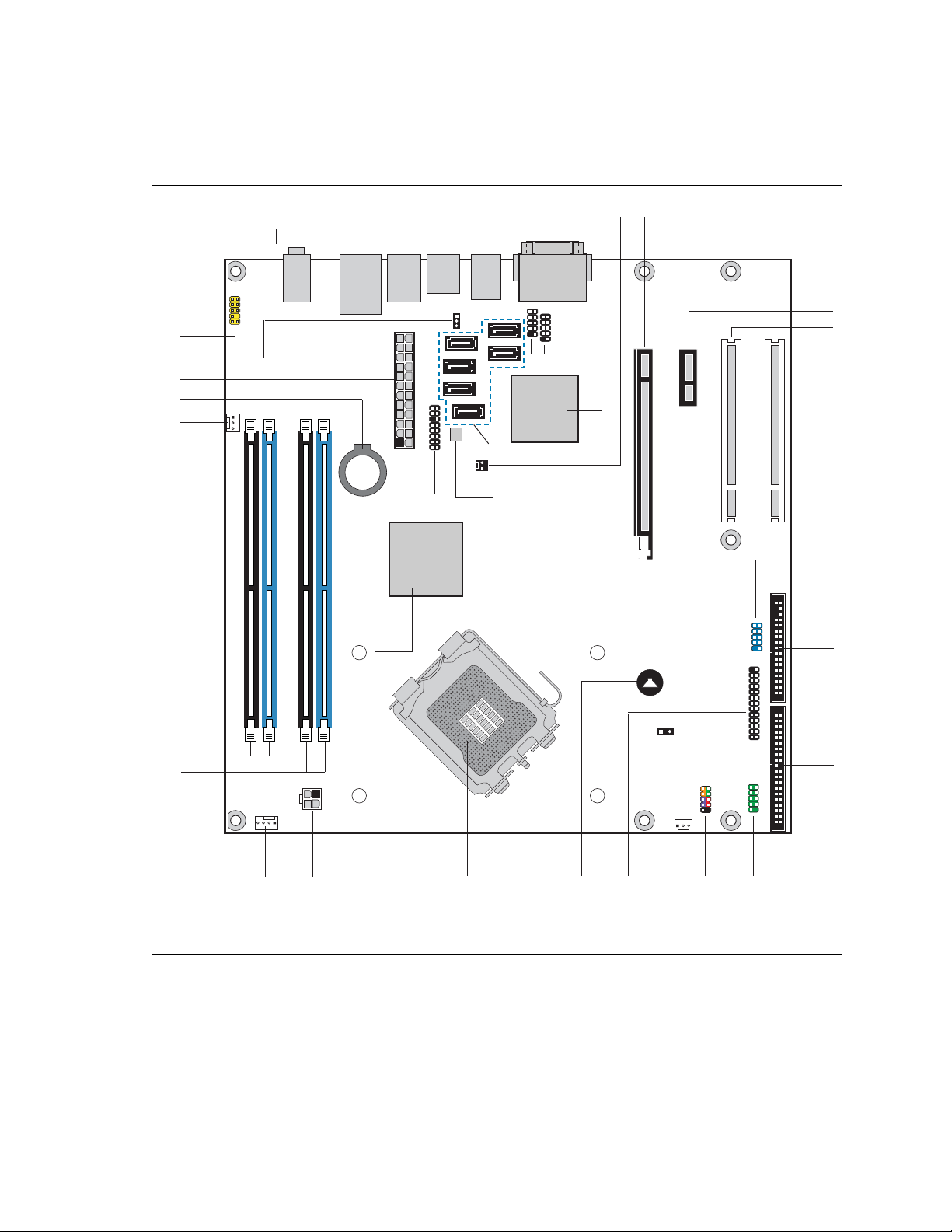
Figure 1 shows the location of the major components.
DD
CC
BB
AA
A
FG
H
I
J
E
Z
D
B
C
K
L
Y
X
W
TUV
Figure 1. Major Board Components
Table 3 lists the components identified in Figure 1.
14
M
R
S
PQ
O
N
OM18313
Page 15

Table 3. Board Components Shown in Figure 1
Item/callout
from
Figure 1 Description
A Back panel connectors
B High Definition Audio header
C Remote thermal sensor
D Serial ATA connectors [6]
E Front panel USB headers [2]
F Intel 82801HO I/O Controller Hub (ICH8DO)
G Chassis intrusion header
H PCI Express x16 connector
I PCI Express x1 connector
J PCI Conventional bus add-in card connectors [2]
K IEEE-1394a front panel header
L Diskette drive connector
M Parallel ATE IDE connector
N Serial port header
O Front panel header
P Front chassis fan header
Q Auxiliary front panel power LED header
R Parallel port header
S Speaker
T LGA775 processor socket
U Intel 82Q965 GMCH
V Processor core power connector
W Processor fan header
X DIMM Channel A sockets
Y DIMM Channel B sockets
Z Rear chassis fan header
AA Battery
BB Main Power connector
CC BIOS Setup configuration jumper block
DD Front panel audio header
Product Description
15
Page 16
Intel Desktop Board DQ965CO Technical Product Specification
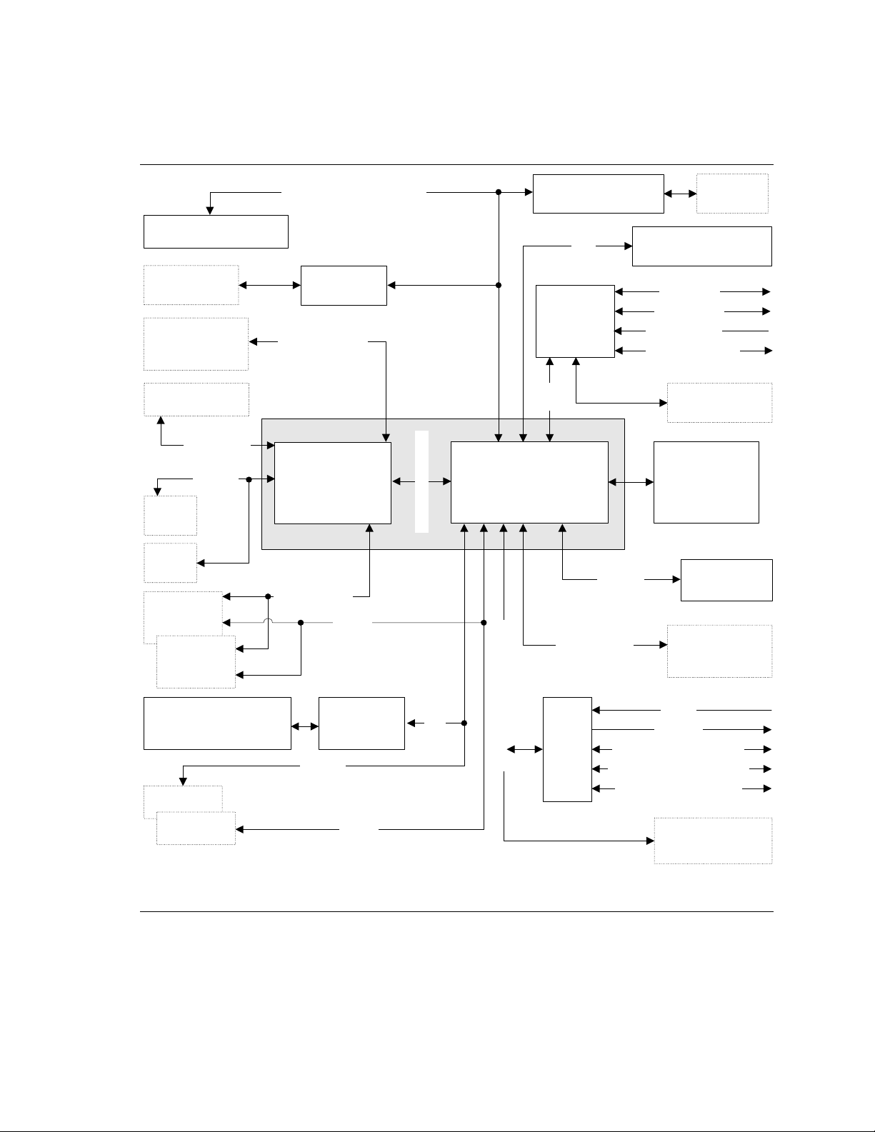
1.1.4 Block Diagram
Figure 2 is a block diagram of the major functional areas.
PCI Express x1 Slot 1
Parallel ATA
IDE
Connector
LGA775
Processor
Socket
PCI Express
x16 Connector
Intel Q965 Express Chipset
PCI Express
x16 Interface
Display
Interface
VGA
Port
DVI
Port
Channel A
DIMMs (2)
Channel B
DIMMs (2)
PCI Express x1 Interface
Parallel ATA
IDE
Controller
System Bus
(1066/800/533
MHz)
Intel 82Q965
Graphics and
Memory
Controller Hub
(GMCH)
Dual-Channel
Memory Bus
SMBus
Gigabit Ethernet
Controller
USB
Legacy
I/O
Controller
LPC
Bus
Intel 82801HO
I/O Controller Hub
(ICH8DO)
DMI Interconnect
LPC Bus
Serial ATA
IDE Interface
Back Panel/Front
USB Ports
Serial Port
Parallel Port
PS/2 Mouse*
PS/2 Keyboard*
Peripheral
Interface (SPI)
Flash Device
Serial ATA IDE
Connectors (6)
LAN
Connector
Panel
Diskette Drive
Connector
Serial
TPM
Component
IEEE-1394a
Connector/Header
PCI Slot 1
PCI Slot 2
IEEE-1394a
Controller
PCI Bus
SMBus
PCI
Bus
* = Optional
Figure 2. Block Diagram
16
Mic In
Audio
Codec
High Definition Audio Link
Line Out/Retasking Jack
Line Out
Line In/Retasking Jack
Mic In/Retasking Jack
High Definition
Audio Link
Header
OM18482
Page 17
Product Description
1.2 Online Support
To find information about… Visit this World Wide Web site:
Intel® Desktop Board DQ965CO under
“Desktop Board Products” or “Desktop
Board Support”
Available configurations for the
Desktop Board DQ965CO
Processor data sheets http://www.intel.com/products/index.htm
ICH8DO addressing http://developer.intel.com/design/chipsets/datashts
Audio software and utilities http://www.intel.com/design/motherbd
LAN software and drivers http://www.intel.com/design/motherbd
Supported video modes http://www.intel.com/design/motherbd/co/co_documentation.htm
http://www.intel.com/design/motherbd
http://support.intel.com/support/motherboards/desktop
http://developer.intel.com/design/motherbd/co/co_available.htm
1.3 Processor
The board is designed to support the following processors:
• Intel Core 2 Duo processor in an LGA775 socket with a 1066 or 800 MHz
system bus
• Intel Pentium D processor in an LGA775 processor socket with an 800 or 533 MHz
system bus
• Intel Pentium 4 processor in an LGA775 processor socket with an 800 or 533 MHz
system bus
• Intel Celeron D processor in an LGA775 processor socket with a 533 MHz
system bus
See the Intel web site listed below for the most up-to-date list of supported
processors.
For information about… Refer to:
Supported processors http://www.intel.com/design/motherbd/co/co_proc.htm
CAUTION
Use only the processors listed on web site above. Use of unsupported processors can
damage the board, the processor, and the power supply.
INTEGRATOR’S NOTE
#
Use only ATX12V-compliant power supplies.
For information about Refer to
Power supply connectors Section 2.7.2.2, page 63
17
Page 18

Intel Desktop Board DQ965CO Technical Product Specification
1.4 System Memory
The board has four DIMM sockets and supports the following memory features:
• 1.8 V (only) DDR2 SDRAM DIMMs with gold-plated contacts
• Unbuffered, single-sided or double-sided DIMMs with the following restriction:
Double-sided DIMMS with x16 organization are not supported.
• 8 GB maximum total system memory using DDR2 667 or DDR2 533 DIMMs;
4 GB maximum total system memory using DDR2 800 DIMMs. Refer to
Section
memory.
• Minimum total system memory: 512 MB
• Non-ECC DIMMs
• Serial Presence Detect
• DDR2 800, DDR2 667, or DDR2 533 MHz SDRAM DIMMs
• DDR2 800 DIMMs with SPD timings of only 5-5-5 or 6-6-6 (tCL-tRCD-tRP)
NOTE
A minimum of 512 MB of system memory is required to fully enable both the onboard
graphics and the manageability engine.
2.1.1 on page 49 for information on the total amount of addressable
NOTE
To be fully compliant with all applicable DDR SDRAM memory specifications, the board
should be populated with DIMMs that support the Serial Presence Detect (SPD) data
structure. This enables the BIOS to read the SPD data and program the chipset to
accurately configure memory settings for optimum performance. If non-SPD memory
is installed, the BIOS will attempt to correctly configure the memory settings, but
performance and reliability may be impacted or the DIMMs may not function under the
determined frequency.
Table 4 lists the supported DIMM configurations.
Table 4. Supported Memory Configurations
DIMM
Type
DDR2 533 256 Mbit 128 MB 512 MB 2 GB
DDR2 533 512 Mbit 256 MB 1 GB 4 GB
DDR2 533 1 Gbit 512 MB 2 GB 8 GB
DDR2 667 256 Mbit 128 MB 512 MB 2 GB
DDR2 667 512 Mbit 256 MB 1 GB 4 GB
DDR2 667 1 Gbit 512 MB 2 GB 8 GB
DDR2 800 256 Mbit 128 MB 512 MB 2 GB
DDR2 800 512 Mbit 256 MB 1 GB 4 GB
SDRAM
Technology
Smallest usable
DIMM (one x16
Single-sided
DIMM)
Largest usable
DIMM (one x8
Double-sided
DIMM)
Maximum capacity
with four identical
x8 Double-sided
DIMMs
18
Page 19

Product Description
NOTE
Regardless of the DIMM type used, the memory frequency will either be equal to or
less than the processor system bus frequency. For example, if DDR2 800 memory is
used with a 533 MHz system bus frequency processor, the memory will operate at
533 MHz.
Table 5 lists the resulting operating memory frequencies based on the
combination of DIMMs and processors.
Table 5. Memory Operating Frequencies
DIMM Type Processor system bus frequency Resulting memory frequency
DDR2 533 533 MHz 533 MHz
DDR2 533 800 MHz 533 MHz
DDR2 533 1066 MHz 533 MHz
DDR2 667 533 MHz 533 MHz
DDR2 667 800 MHz 667 MHz
DDR2 667 1066 MHz 667 MHz
DDR2 800 533 MHz 533 MHz
DDR2 800 800 MHz 800 MHz
DDR2 800 1066 MHz 800 MHz
19
Page 20
Intel Desktop Board DQ965CO Technical Product Specification
1.4.1 Memory Configurations
The Intel 82Q965 GMCH supports the following types of memory organization:
• Dual channel (Interleaved) mode. This mode offers the highest throughput for
real world applications. Dual channel mode is enabled when the installed memory
capacities of both DIMM channels are equal. Technology and device width can vary
from one channel to the other but the installed memory capacity for each channel
must be equal. If different speed DIMMs are used between channels, the slowest
memory timing will be used.
• Single channel (Asymmetric) mode. This mode is equivalent to single channel
bandwidth operation for real world applications. This mode is used when only a
single DIMM is installed or the memory capacities are unequal. Technology and
device width can vary from one channel to the other. If different speed DIMMs are
used between channels, the slowest memory timing will be used.
• Flex mode. This mode provides the most flexible performance characteristics.
The bottommost DRAM memory (the memory that is lowest within the system
memory map) is mapped to dual channel operation; the topmost DRAM memory
(the memory that is nearest to the 8 GB address space limit), if any, is mapped to
single channel operation. Flex mode results in multiple zones of dual and single
channel operation across the whole of DRAM memory. To use flex mode, it is
necessary to populate both channels.
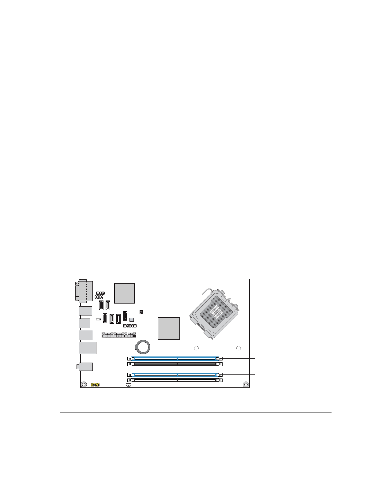
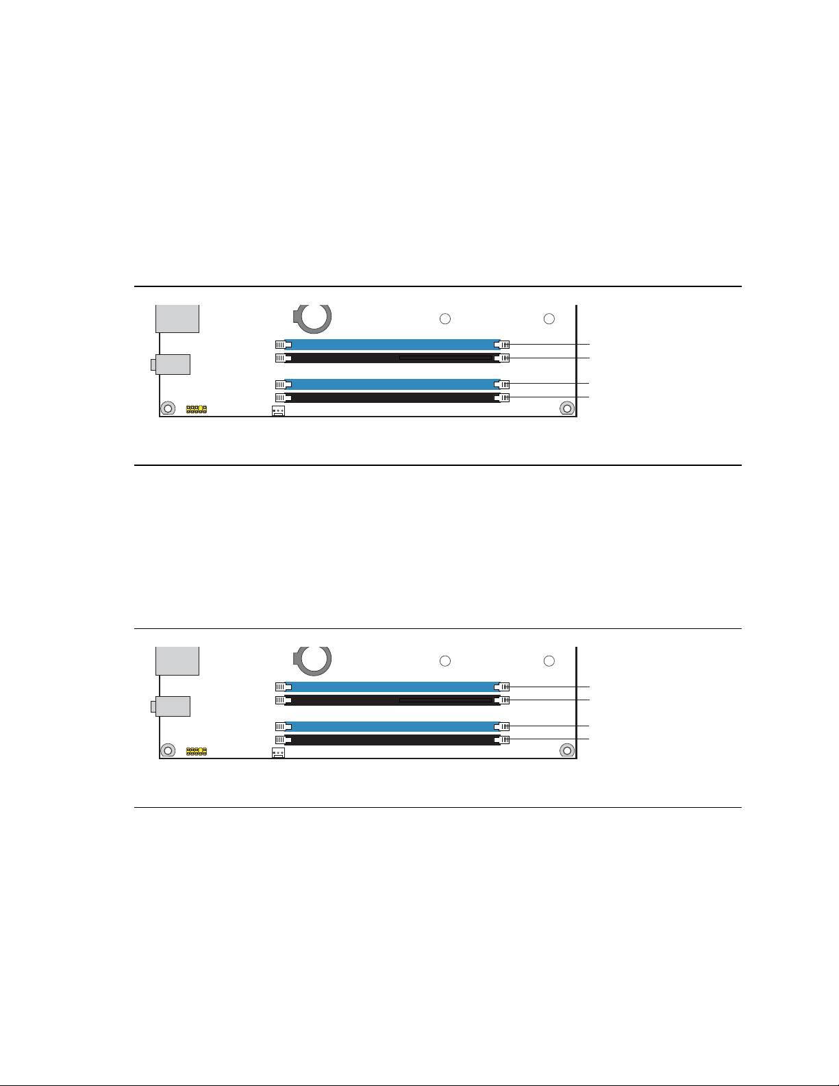
Figure 3 illustrates the memory channel and DIMM configuration.
NOTE
The DIMM0 sockets of both channels are blue. The DIMM1 sockets of both channels
are black.
Channel A, DIMM 0
Channel A, DIMM 1
Channel B, DIMM 0
Channel B, DIMM 1
Figure 3. Memory Channel Configuration and DIMM Configuration
20
OM18322
Page 21
Product Description
INTEGRATOR’S NOTE
#
Regardless of the memory configuration used (dual channel, single channel, or flex
mode), DIMM 0 of Channel A must always be populated. This is a requirement of the
ICH8 Manageability Engine feature.
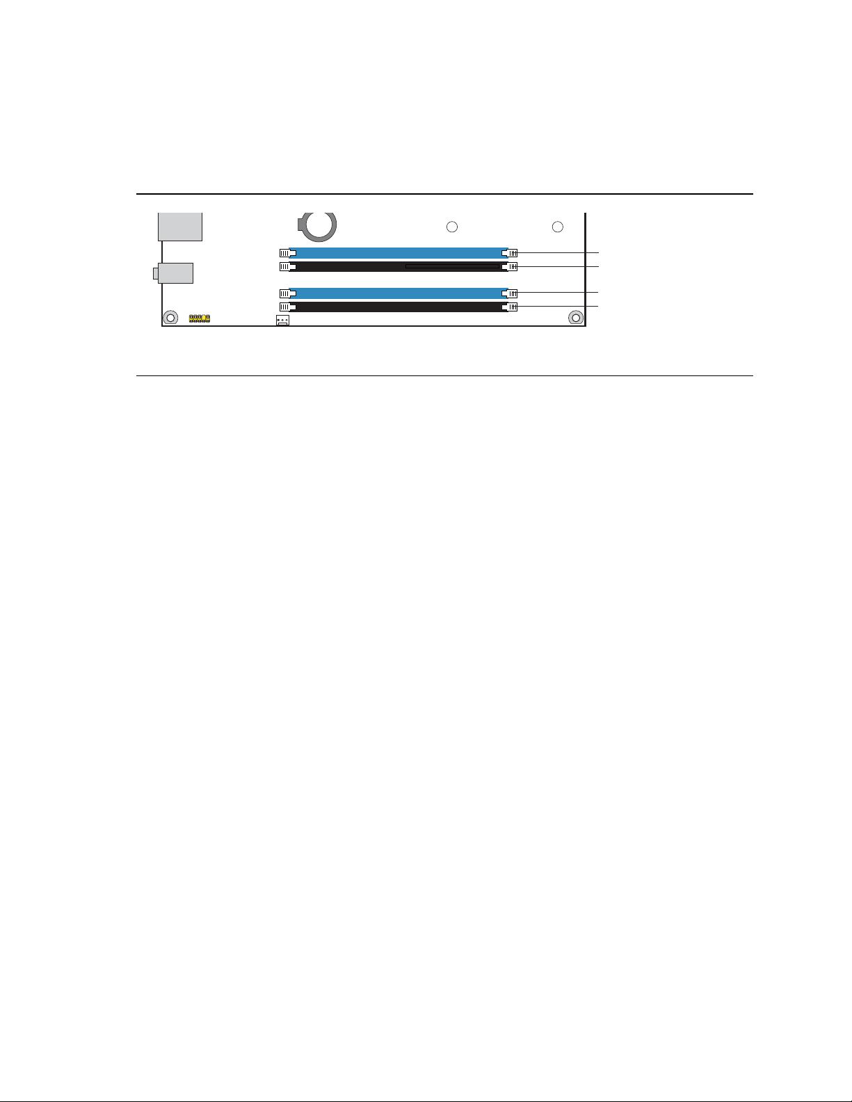
1.4.1.1 Dual Channel (Interleaved) Mode Configurations
Figure 4 shows a dual channel configuration using two DIMMs. In this example, the
DIMM0 (blue) sockets of both channels are populated with identical DIMMs.
1 GB
Channel A, DIMM 0
Channel A, DIMM 1
1 GB
Channel B, DIMM 0
Channel B, DIMM 1
OM18323
Figure 4. Dual Channel (Interleaved) Mode Configuration
with Two DIMMs
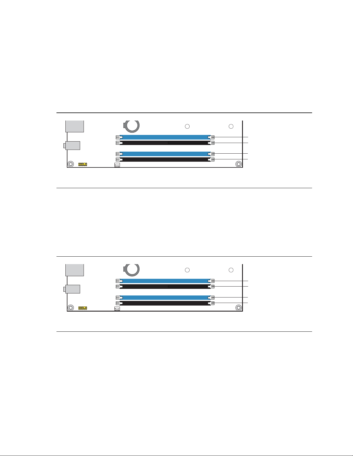
Figure 5 shows a dual channel configuration using three DIMMs. In this example, the
combined capacity of the two DIMMs in Channel A equal the capacity of the single
DIMM in the DIMM0 (blue) socket of Channel B.
256 MB
256 MB
512 MB
Channel A, DIMM 0
Channel A, DIMM 1
Channel B, DIMM 0
Channel B, DIMM 1
Figure 5. Dual Channel (Interleaved) Mode Configuration
with Three DIMMs
21
OM18324
Page 22
Intel Desktop Board DQ965CO Technical Product Specification
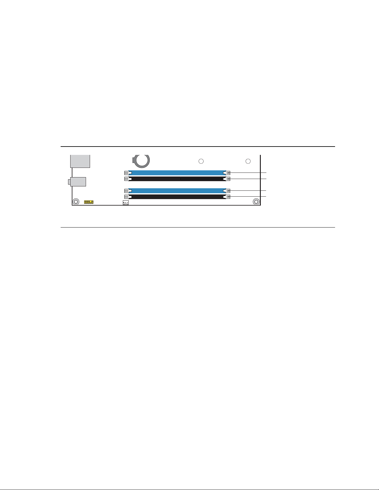
Figure 6 shows a dual channel configuration using four DIMMs. In this example, the
combined capacity of the two DIMMs in Channel A equal the combined capacity of the
two DIMMs in Channel B. Also, the DIMMs are matched between DIMM0 and DIMM1
of both channels.
256 MB
512 MB
256 MB
512 MB
Channel A, DIMM 0
Channel A, DIMM 1
Channel B, DIMM 0
Channel B, DIMM 1
Figure 6. Dual Channel (Interleaved) Mode Configuration
with Four DIMMs
OM18325
22
Page 23
Product Description
1.4.1.2 Single Channel (Asymmetric) Mode Configurations
NOTE
Dual channel (Interleaved) mode configurations provide the highest memory
throughput.
Figure 7 shows a single channel configuration using one DIMM. In this example, only
the DIMM0 (blue) socket of Channel A is populated. Channel B is not populated.
512 MB
Channel A, DIMM 0
Channel A, DIMM 1
Channel B, DIMM 0
Channel B, DIMM 1
OM18326
Figure 7. Single Channel (Asymmetric) Mode Configuration
with One DIMM
Figure 8 shows a single channel configuration using three DIMMs. In this example, the
combined capacity of the two DIMMs in Channel A does not equal the capacity of the
single DIMM in the DIMM0 (blue) socket of Channel B.
256 MB
512 MB
512 MB
Channel A, DIMM 0
Channel A, DIMM 1
Channel B, DIMM 0
Channel B, DIMM 1
Figure 8. Single Channel (Asymmetric) Mode Configuration
with Three DIMMs
23
OM18327
Page 24
Intel Desktop Board DQ965CO Technical Product Specification
1.4.1.3 Flex Mode Configuration
NOTE
The use of flex mode requires DIMMs to be installed in both channels.
Figure 9 shows a flex mode configuration using two DIMMs. The operation is as
follows:
• The 512 MB DIMM in the Channel A, DIMM 0 socket and the lower 512 MB of the
DIMM in the Channel B, DIMM 0 socket operate together in dual channel mode.
• The remaining (upper) 512 MB of the DIMM in Channel B operates in single
channel mode.
512 MB
1 GB
Figure 9. Flex Mode Configuration with Two DIMMs
Channel A, DIMM 0
Channel A, DIMM 1
Channel B, DIMM 0
Channel B, DIMM 1
OM18405
24
Page 25

Product Description
1.5 Intel® Virtualization Technology (Intel® VT)
Virtualization is a proven technology that enables one computer to function as multiple
“virtual” systems. It enables multiple operating systems and application stacks to be
hosted in logically isolated partitions — also known as virtual machines. Partitions are
independent virtualized environments within the same PC with shared, prioritized
access to system hardware. Platform resources, such as processors, memory,
storage, and network adapters can be allocated and prioritized for the different
partitions to meet specific business and application requirements.
®
Intel
virtualization processes and a new, dedicated space in the software stack for an Intel
Lightweight Virtual Machine Monitor (Intel
and prioritizes each partition’s access to the system hardware.
Intel provides the virtualization capability within Intel Virtualization Technologyenabled processors and validated chipsets. An Intel Virtualization Technology-enabled
BIOS is also needed. Standard memory, storage, and graphics cards work with the
Intel Virtualization Technology solution. However, because the quality and amount of
such system resources directly affect virtualization performance, it is advisable to be
generous in these areas. Using an Intel
ensures the ability to take advantage of the advanced security and manageability
capabilities of Intel Virtualization Technology.
Virtualization Technology (Intel® VT) offers silicon-level support for core
®
LVMM) — a software layer that controls
®
network adapter and compatible driver
®
A Virtual Machine Monitor enabled for Intel Virtualization Technology, such as
Intel LVMM, is also required. Intel LVMM is available to Independent Software Vendors
(ISVs). After the system hardware and Intel LVMM are in place, Intel Virtualization
Technology-enabled applications will need to be installed to take advantage of the
built-in hardware capabilities of Intel Virtualization Technology and the virtualization
enhancement of Intel LVMM.
For information about Refer to
Intel Virtualization Technology http://www.intel.com/go/dovirtualization/
INTEGRATOR’S NOTE
#
Intel Virtualization Technology-based platforms require system hardware,
virtualization software, and applications that are enabled for Intel Virtualization
Technology.
Individual PC manufacturers will determine whether to ship their platforms with Intel
Virtualization Technology enabled or disabled by default. Also, each PC manufacturer
may choose to ship Intel LVMM already installed on their platforms or on separate
CD-ROMs.
25
Page 26

Intel Desktop Board DQ965CO Technical Product Specification
1.6 Intel® vPro™ Technology Support
The board supports Intel vPro technology, Intel’s platform for the digital office.
Intel vPro technology with Active Management Technology provides remote
management, improved security, and energy-efficient performance.
The management engine microcontroller in the Intel Q965 Express Chipset provides
remote hardware management capabilities regardless of the state of the operating
system. The embedded packet filters and sensors in ICH8DO provide enhanced
security features customizable through third party applications.
INTEGRATOR’S NOTE
#
In addition to the hardware support on the board (the Intel 82801HO ICH8DO and the
Intel 82566DM Gigabit Ethernet Controller), Intel vPro technology requires the use of
an Intel Core 2 Duo processor and compatible third-party applications.
For information about Refer to
Intel vPro technology and compatible third-party applications http://www.intel.com/vpro/
26
Page 27

Product Description
1.7 Intel® Q965 Express Chipset
The Intel Q965 Express chipset consists of the following devices:
• Intel 82Q965 Graphics and Memory Controller Hub (GMCH) with Direct Media
Interface (DMI) interconnect
• Intel 82801HO I/O Controller Hub (ICH8DO) with DMI interconnect
The GMCH component provides interfaces to the CPU, memory, PCI Express, and the
DMI interconnect. The component also provides integrated graphics capabilities
supporting 3D, 2D and display capabilities. The ICH8DO is a centralized controller for
the board’s I/O paths.
For information about Refer to
The Intel Q965 Express chipset http://developer.intel.com/
Resources used by the chipset Chapter 2
1.7.1 Intel Q965 Graphics Subsystem
The Intel Q965 Express chipset contains two separate, mutually exclusive graphics
options. Either the GMA 3000 graphics controller (contained within the 82Q965
GMCH) is used, or a PCI Express x16 add-in card can be used. When a PCI Express
x16 add-in card is installed, the GMA 3000 graphics controller is disabled.
1.7.1.1 Intel® GMA 3000 Graphics Controller
The Intel GMA 3000 graphics controller features the following:
• 667 MHz core frequency
• High performance 3-D setup and render engine
• High quality texture engine
⎯ DX9.0c* and OpenGL* 1.4 + extensions compliant
⎯ Vertex Shader Model 2.0 / 3.0 (Software Only)
⎯ Hardware Pixel Shader 2.0
⎯ 32-bit and 16-bit Full Precision Floating Point Operations
⎯ Up to eight Multiple Render Targets (MRTs)
⎯ Occlusion Query
⎯ 128-bit floating point texture formats
⎯ Bilinear, Trilinear, and Anisotropic MipMap filtering
⎯ Shadow maps and double sided stencils
⎯ Alpha and luminance maps
⎯ Texture color-keying/chroma-keying
⎯ Cubic environment reflection mapping
⎯ Enhanced texture blending functions
• 3D Graphics Rendering enhancements
⎯ 1.3 dual texture GigaPixel/sec fill rate
⎯ 16 and 32 bit color
27
Page 28

Intel Desktop Board DQ965CO Technical Product Specification
⎯ Maximum 3D supported resolution of 1600 x 1200 x 32 at 85 Hz
⎯ Vertex cache
⎯ Anti-aliased lines
⎯ OpenGL version 1.5 support with vertex buffer and EXT_Shadow extensions
• 2D Graphics enhancements
⎯ 8, 16, and 32 bit color
⎯ Optimized 256-bit BLT engine
⎯ Color space conversion
⎯ Anti-aliased lines
• Video
⎯ Hardware motion compensation for MPEG2 and HD video
⎯ Software DVD at 30 fps full screen
⎯ Motion adaptive de-interlacing
• Display
⎯ Integrated 24-bit 400 MHz RAMDAC
⎯ Up to 2048 x 1536 at 75 Hz refresh (QXGA)
⎯ DVI specification 1.0 compliant
⎯ Dual independent display options with digital display
⎯ 180-degree hardware screen rotation
⎯ Hardware color cursor support
⎯ Supports TMDS transmitters or TV-out encoders
⎯ HDCP support
⎯ DDC2B compliant interface with Advanced Digital Display 2 card or Media
Expansion Card (ADD2/MEC), support for TV-out/TV-in and DVI digital display
connections
⎯ Supports flat panels up to 2048 x 1536 at 75 Hz (when in dual-channel mode)
or digital CRT/HDTV at 1920 x 1080 at 85 Hz (with ADD2/MEC)
⎯ Two multiplexed SDVO port interfaces with 270 MHz pixel clocks using an
ADD2/MEC card
• Dynamic Video Memory Technology (DVMT) support up to 256 MB
®
• Intel
Zoom Utility
1.7.1.2 Dynamic Video Memory Technology (DVMT)
DVMT enables enhanced graphics and memory performance through highly efficient
memory utilization. DVMT ensures the most efficient use of available system memory
for maximum 2-D/3-D graphics performance. Up to 256 MB of system memory can be
allocated to DVMT on systems that have 512 MB or more of total system memory
installed. DVMT returns system memory back to the operating system when the
additional system memory is no longer required by the graphics subsystem.
DVMT will always use a minimal fixed portion of system physical memory (as set in the
BIOS Setup program) for compatibility with legacy applications. An example of this
would be when using VGA graphics under DOS. Once loaded, the operating system
28
Page 29

Product Description
and graphics drivers allocate additional system memory to the graphics buffer as
needed for performing graphics functions.
NOTE
The use of DVMT requires operating system driver support.
1.7.1.3 Configuration Modes
A list of supported modes for the Intel GMA 3000 graphics controller is available as a
downloadable document.
For information about Refer to
Supported video modes for the board Section 1.2, page 17
1.7.1.4 Digital Video Interface (DVI)
The DVI port supports only DVI-D displays. If a DVI-I display is connected, only the
digital signal will be displayed. The maximum supported resolution is 1600 x 1200 at
60 Hz. The DVI port is compliant with the following specifications:
• DVI 1.0
• HDCP rev 1.1 down-stream compliant (when applicable)
Depending on the type of add-in card installed in the PCI Express x16 connector, the
DVI port will behave as described in
Table 6. DVI Port Status Conditions
PCI Express x16 connector status DVI port status
No add-in card installed Enabled
Non-video PCI Express x1 add-in card installed Enabled
PCI Express x4, x8, or 16 add-in card installed Disabled
ADD2 or MEC card installed Disabled
Table 6.
1.7.1.5 Advanced Digital Display (ADD2/MEC) Card Support
The GMCH routes two multiplexed SDVO ports that are each capable of driving up to a
200 MHz pixel clock to the PCI Express x16 connector. The SDVO ports can be paired
for a dual channel configuration to support up to a 400 MHz pixel clock. When an
ADD2/MEC card is detected, the Intel GMA 3000 graphics controller is enabled and the
PCI Express x16 connector is configured for SDVO mode. SDVO mode enables the
SDVO ports to be accessed by the ADD2/MEC card. An ADD2/MEC card can either be
configured to support simultaneous display with the primary VGA display or can be
configured to support dual independent display as an extended desktop configuration
with different color depths and resolutions. ADD2/MEC cards can be designed to
support the following configurations:
• TV-Out (composite video)
• Transition Minimized Differential Signaling (TMDS) for DVI 1.0
• Low Voltage Differential Signaling (LVDS)
29
Page 30

Intel Desktop Board DQ965CO Technical Product Specification
• Single device operating in dual channel mode
• VGA output
• HDTV output
• HDMI/UDI support (when used with the HD Audio Link)
1.7.2 USB
The board supports up to 10 USB 2.0 ports, supports UHCI and EHCI, and uses UHCIand EHCI-compatible drivers.
The ICH8DO provides the USB controller for all ports. The port arrangement is as
follows:
• Six ports are implemented with stacked back panel connectors
• Four ports are routed to two separate front panel USB headers
NOTE
Computer systems that have an unshielded cable attached to a USB port may not
meet FCC Class B requirements, even if no device is attached to the cable. Use
shielded cable that meets the requirements for full-speed devices.
For information about Refer to
The location of the USB connectors on the back panel Figure 15, page 57
The location of the front panel USB headers Figure 16, page 58
1.7.3 Serial ATA Interfaces
The board provides six Serial ATA (SATA) connectors, which support one device per
connector.
1.7.3.1 Serial ATA Support
The ICH8DO’s Serial ATA controller offers six independent Serial ATA ports with a
theoretical maximum transfer rate of 3 Gbits/sec per port. One device can be installed
on each port for a maximum of six Serial ATA devices. A point-to-point interface is
used for host to device connections, unlike Parallel ATA IDE which supports a
master/slave configuration and two devices per channel.
For compatibility, the underlying Serial ATA functionality is transparent to the
operating system. The Serial ATA controller can operate in both legacy and native
modes. In legacy mode, standard IDE I/O and IRQ resources are assigned (IRQ 14
and 15). In Native mode, standard PCI Conventional bus resource steering is used.
Native mode is the preferred mode for configurations using the Windows* XP and
Windows 2000 operating systems.
30
Page 31

Product Description
NOTE
Many Serial ATA drives use new low-voltage power connectors and require adaptors or
power supplies equipped with low-voltage power connectors.
For more information, see:
For information about Refer to
The location of the Serial ATA connectors Figure 16, page 58
http://www.serialata.org/
1.7.3.2 Serial ATA RAID
The ICH8DO supports the following RAID (Redundant Array of Independent Drives)
levels:
• RAID 0 - data striping
• RAID 1 - data mirroring
• RAID 0+1 (or RAID 10) - data striping and mirroring
• RAID 5 - distributed parity
1.7.4 Parallel IDE Interface
The Parallel ATA IDE controller has one bus-mastering Parallel ATA IDE interface. The
Parallel ATA IDE interface supports the following modes:
• Programmed I/O (PIO): processor controls data transfer.
• 8237-style DMA: DMA offloads the processor, supporting transfer rates of up to
16 MB/sec.
• Ultra DMA: DMA protocol on IDE bus supporting host and target throttling and
transfer rates of up to 33 MB/sec.
• ATA-66: DMA protocol on IDE bus supporting host and target throttling and
transfer rates of up to 66 MB/sec. ATA-66 protocol is similar to Ultra DMA and is
device driver compatible.
• ATA-100: DMA protocol on IDE bus allows host and target throttling. The ATA-100
logic can achieve read transfer rates up to 100 MB/sec and write transfer rates up
to 88 MB/sec.
• ATA-133: DMA protocol on IDE bus allows host and target throttling. The ATA-133
logic is designed to achieve read transfer rates up to 133 MB/sec and write transfer
rates in excess of 100 MB/sec.
NOTE
ATA-66, ATA-100, and ATA-133 are faster timings and require a specialized cable to
reduce reflections, noise, and inductive coupling.
The Parallel ATA IDE interface also supports ATAPI devices (such as CD-ROM drives)
and ATA devices. The BIOS supports Logical Block Addressing (LBA) and Extended
Cylinder Head Sector (ECHS) translation modes. The drive reports the transfer rate
and translation mode to the BIOS.
For information about Refer to
The location of the Parallel ATA IDE connector Figure 16, page 58
31
Page 32

Intel Desktop Board DQ965CO Technical Product Specification
1.7.5 Real-Time Clock, CMOS SRAM, and Battery
A coin-cell battery (CR2032) powers the real-time clock and CMOS memory. When
the computer is not plugged into a wall socket, the battery has an estimated life of
three years. When the computer is plugged in, the standby current from the power
supply extends the life of the battery. The clock is accurate to ± 13 minutes/year at
25 ºC with 3.3 VSB applied.
NOTE
If the battery and AC power fail, custom defaults, if previously saved, will be loaded
into CMOS RAM at power-on.
When the voltage drops below a certain level, the BIOS Setup program settings stored
in CMOS RAM (for example, the date and time) might not be accurate. Replace the
battery with an equivalent one.
1.8 Legacy I/O Controller
The I/O controller provides the following features:
• One serial port
• One parallel port with Extended Capabilities Port (ECP) and Enhanced Parallel Port
(EPP) support
• Serial IRQ interface compatible with serialized IRQ support for PCI systems
• PS/2-style mouse and keyboard interfaces
• Interface for one 1.44 MB or 2.88 MB diskette drive
• Intelligent power management, including a programmable wake-up event interface
• PCI power management support
Figure 1 on page 14 shows the location of the battery.
The BIOS Setup program provides configuration options for the I/O controller.
1.8.1 Serial Port Interface
The serial port header is located on the component side of the board. The serial port
supports data transfers at speeds up to 115.2 kbits/sec with BIOS support.
For information about Refer to
The location of the serial port header Figure 16, page 58
32
Page 33

Product Description
1.8.2 Parallel Port Interface
The parallel port header is located on the component side of the board. Use the BIOS
Setup program to set the parallel port mode.
For information about Refer to
The location of the parallel port header Figure 16, page 58
1.8.3 Diskette Drive Interface
The I/O controller supports one diskette drive. Use the BIOS Setup program to
configure the diskette drive interface.
For information about Refer to
The location of the diskette drive connector Figure 16, page 58
1.8.4 PS/2 Keyboard and Mouse Interface (Optional)
The optional PS/2 keyboard and mouse connectors are located on the back panel.
NOTE
The keyboard is supported in the bottom PS/2 connector and the mouse is supported
in the top PS/2 connector. Power to the computer should be turned off before a
keyboard or mouse is connected or disconnected.
For information about Refer to
The location of the optional keyboard and mouse connectors Figure 15, page 57
33
Page 34

Intel Desktop Board DQ965CO Technical Product Specification
1.9 Audio Subsystem
The onboard audio subsystem consists of the following:
• Intel 82801HO ICH8DO
• Sigmatel STAC9227 audio codec
• Back panel audio connectors
• Component-side audio headers:
⎯ Front panel audio header
⎯ HD audio link header
The audio subsystem supports the following features:
• Advanced jack sense for the front/back panel audio jacks that enables the audio
codec to recognize the device that is connected to an audio port. Within hardware
constraints, the back panel audio jacks are capable of retasking according to the
user’s definition, or can be automatically switched depending on the recognized
device type.
• A signal-to-noise (S/N) ratio of 95 dB
Table 7 lists the supported retasking functions of the front panel and back panel audio
jacks.
Table 7. Audio Jack Retasking Support
Audio Jack
Front panel – Green Yes Yes No Yes
Front panel – Pink Yes No Yes No
Back panel – Blue Yes Yes No No
Back panel – Green No Yes No Yes
Back panel – Pink Yes Yes Yes No
Supports
Line in?
Supports
Line out?
Supports
Microphone?
1.9.1 Audio Subsystem Software
Audio software and drivers are available from Intel’s World Wide Web site.
For information about Refer to
Obtaining audio software and drivers Section
Supports
Headphones?
1.2, page 17
34
Page 35

Product Description
k
1.9.2 Audio Connectors and Headers
The board contains audio connectors and headers on both the back panel and the
component side of the board. The front panel audio header provides mic in and line
out signals for the front panel. Microphone bias is supported for both the front and
back panel microphone connectors.
The front/back panel audio connectors are configurable through the audio device
drivers. The available configurable audio ports are shown in
Figure 10.
Front Panel Audio Connectors
[Routed from Front Panel Audio Header]
Line Out/
Retasking Jac
[Green]
Mic In/
Retasking Jack
[Pink]
Back Panel Audio Connectors
Line In/Retasking Jack
[Blue]
Line Out/Retasking Jack
[Green]
Mic In/Retasking Jack
[Pink]
OM18469
Figure 10. Front/Back Panel Audio Connector Options
For information about Refer to
The location of the front panel audio header Figure 16, page 58
The signal names of the front panel audio header Table 26, page 61
The location of the HD Audio Link header Figure 16, page 58
The signal names of the HD Audio Link header Table 19, page 60
The back panel audio connectors Section 2.7.1, page 57
35
Page 36

Intel Desktop Board DQ965CO Technical Product Specification
1.10 LAN Subsystem
The LAN subsystem consists of the following:
• Intel 82566DM Gigabit (10/100/1000 Mbits/sec) Ethernet LAN controller
• Intel 82801HO ICH8DO
• RJ-45 LAN connector with integrated status LEDs
Additional features of the LAN subsystem include:
• CSMA/CD protocol engine
• LAN connect interface between ICH8DO and LAN controller
• PCI Conventional bus power management
⎯ Supports ACPI technology
⎯ Supports LAN wake capabilities
⎯ LAN Subsystem Software
LAN software and drivers are available from Intel’s World Wide Web site.
1.10.1 Intel® 82566DM Gigabit Ethernet Controller
The Intel 82566DM Gigabit Ethernet Controller supports the following features:
• PCI Express link
• 10/100/1000 IEEE 802.3 compliant
• Compliant to IEEE 802.3x flow control support
• Jumbo frame support
• TCP, IP, UDP checksum offload
• Transmit TCP segmentation
• Advanced packet filtering
• Full device driver compatibility
• PCI Express Power Management Support
The Intel 82566DM also provides support for:
• Alert Standard Format (ASF) 2.0
• Intel
• Virtual LAN driver support for Intel VT partitions
®
Active Management Technology (Intel® AMT)
1.10.2 LAN Subsystem Software
LAN software and drivers are available from Intel’s World Wide Web site.
For information about Refer to
Obtaining LAN software and drivers Section
1.2, page 17
36
Page 37

Product Description
1.10.3 RJ-45 LAN Connector with Integrated LEDs
Two LEDs are built into the RJ-45 LAN connector (shown in Figure 11 below).
Link LED
(Green)
Data Rate LED
(Green/Yellow)
OM18329
Figure 11. LAN Connector LED Locations
Table 8 describes the LED states when the board is powered up and the LAN
subsystem is operating.
Table 8. LAN Connector LED States
LED LED Color LED State Condition
Off LAN link is not established.
Link Green
Data Rate Green/Yellow
On LAN link is established.
Blinking LAN activity is occurring.
Off 10 Mbits/sec data rate is selected.
Green 100 Mbits/sec data rate is selected.
Yellow 1000 Mbits/sec data rate is selected.
1.10.4 Intel® Active Management Technology
(Intel
®
AMT) with System Defense Feature
Intel Active Management Technology offers IT organizations tamper-resistant and
persistent management capabilities. Specifically, Intel AMT is a hardware-based
solution that uses out of band communication to manage access client systems in
addition to offering encrypted and persistent asset management and remote
diagnostics and/or recovery capabilities for networked platforms. With Intel AMT, IT
organizations can easily get accurate platform information, and can perform remote
updating, diagnostics, debugging and repair of a system, regardless of the state of the
operating system and the power state of the system.
NOTE
Software with AMT capability is required to take advantage of Intel AMT platform
management capabilities.
The key features of Intel AMT include:
• Secure Out of Band (OOB) system management that allows remote management
of PCs regardless of system power or operating system state.
• Remote troubleshooting and recovery that can significantly reduce desk-side visits
and potentially increasing efficiency of IT technical staff.
• Proactive alerting that decreases downtime and minimizes time to repair.
37
Page 38

Intel Desktop Board DQ965CO Technical Product Specification
• Third party non-volatile storage that prevents users from removing critical
inventory, remote control, or virus protection agents.
• Remote hardware and software asset tracking that eliminates time-consuming
manual inventory tracking, which also reduces asset accounting costs.
• System Defense Feature - an Intel AMT feature for stopping the propagation of
worms and viruses through the use of programmable packet filters in the
integrated LAN controller. The packet filters inspect all incoming and all outgoing
packets and determine whether to block or pass the packets as configured. There
is no indication to the host that a packet has been blocked or accepted.
For information about Refer to
Intel Active Management
Technology
http://www.intel.com/technology/manage/iamt/index.htm
1.10.5 Alert Standard Format (ASF) 2.0 Support
The board provides the following ASF support for PCI Express x1 bus add-in LAN cards
and PCI Conventional bus add-in LAN cards:
• Monitoring of system firmware progress events, including:
⎯ BIOS present
⎯ Primary processor initialization
⎯ Memory initialization
⎯ Video initialization
⎯ PCI resource configuration
⎯ Hard-disk initialization
⎯ User authentication
⎯ Starting operating system boot process
• Monitoring of system firmware error events, including:
⎯ Memory missing
⎯ Memory failure
⎯ No video device
⎯ Keyboard failure
⎯ Hard-disk failure
⎯ No boot media
• Boot options to boot from different types of boot devices
• Reset, shutdown, power cycle, and power up options
• LAN Subsystem Software
LAN software and drivers are available from Intel’s World Wide Web site.
38
Page 39

Product Description
1.11 Hardware Management Subsystem
The hardware management features enable the board to be compatible with the Wired
for Management (WfM) specification. The board has several hardware management
features, including the following:
• Fan monitoring and control
• Thermal and voltage monitoring
• Chassis intrusion detection
1.11.1 Hardware Monitoring and Fan Control
The features of the hardware monitoring and fan control include:
• Intel Quiet System Technology, delivering acoustically-optimized thermal
management
• Fan speed control controllers and sensors integrated into the ICH8DO
• Four thermal sensors (processor, 82Q965 GMCH, 82801HO ICH8DO, and a remote
thermal sensor)
• Power supply monitoring of five voltages (+5 V, +12 V, +3.3 VSB, +1.25 V, and
+VCCP) to detect levels above or below acceptable values
• Thermally monitored closed-loop fan control, for all three fans, that can adjust the
fan speed or switch the fans on or off as needed
1.11.2 Fan Monitoring
Fan monitoring can be implemented using Intel Desktop Utilities or third-party
software.
For information about Refer to
The functions of the fan headers Section 1.12.2.2, page 44
1.11.3 Chassis Intrusion and Detection
The board supports a chassis security feature that detects if the chassis cover is
removed. The security feature uses a mechanical switch on the chassis that attaches
to the chassis intrusion header. When the chassis cover is removed, the mechanical
switch is in the closed position.
For information about Refer to
The location of the chassis intrusion header Figure 16, page 58
39
Page 40

Intel Desktop Board DQ965CO Technical Product Specification
1.11.4 Thermal Monitoring
Figure 12 shows the locations of the thermal sensors and fan headers.
C
G
D
E
Item Description
A Thermal diode, located on processor die
B Thermal diode, located on the GMCH die
C Thermal diode, located on the ICH8DO die
D Remote thermal sensor
E Processor fan
F Front chassis fan
G Rear chassis fan
AB
F
Figure 12. Thermal Sensors and Fan Headers
OM18314
40
Page 41

Product Description
1.12 Power Management
Power management is implemented at several levels, including:
• Software support through Advanced Configuration and Power Interface (ACPI)
• Hardware support:
⎯ Power connector
⎯ Fan headers
⎯ LAN wake capabilities
⎯ Instantly Available PC technology
⎯ Resume on Ring
⎯ Wake from USB
⎯ Wake from PS/2 devices
⎯ Power Management Event signal (PME#) wake-up support
1.12.1 ACPI
ACPI gives the operating system direct control over the power management and Plug
and Play functions of a computer. The use of ACPI with the board requires an
operating system that provides full ACPI support. ACPI features include:
• Plug and Play (including bus and device enumeration)
• Power management control of individual devices, add-in boards (some add-in
boards may require an ACPI-aware driver), video displays, and hard disk drives
• Methods for achieving less than 15-watt system operation in the power-on/standby
sleeping state
• A Soft-off feature that enables the operating system to power-off the computer
• Support for multiple wake-up events (see
• Support for a front panel power and sleep mode switch
Table 11 on page 43)
Table 9 lists the system states based on how long the power switch is pressed,
depending on how ACPI is configured with an ACPI-aware operating system.
Table 9. Effects of Pressing the Power Switch
If the system is in this
state…
Off
(ACPI G2/G5 – Soft off)
On
(ACPI G0 – working state)
On
(ACPI G0 – working state)
Sleep
(ACPI G1 – sleeping state)
Sleep
(ACPI G1 – sleeping state)
…and the power switch
is pressed for
Less than four seconds Power-on
Less than four seconds Soft-off/Standby
More than four seconds Fail safe power-off
Less than four seconds Wake-up
More than four seconds Power-off
…the system enters this state
(ACPI G0 – working state)
(ACPI G1 – sleeping state)
(ACPI G2/G5 – Soft off)
(ACPI G0 – working state)
(ACPI G2/G5 – Soft off)
41
Page 42

Intel Desktop Board DQ965CO Technical Product Specification
1.12.1.1 System States and Power States
Under ACPI, the operating system directs all system and device power state
transitions. The operating system puts devices in and out of low-power states based
on user preferences and knowledge of how devices are being used by applications.
Devices that are not being used can be turned off. The operating system uses
information from applications and user settings to put the system as a whole into a
low-power state.
Table 10 lists the power states supported by the board along with the associated
system power targets. See the ACPI specification for a complete description of the
various system and power states.
Table 10. Power States and Targeted System Power
Global
States
G0 – working
state
G1 – sleeping
state
G1 – sleeping
state
G1 – sleeping
state
G2/S5 S5 – Soft off.
G3 –
mechanical off.
AC power is
disconnected
from the
computer.
Notes:
1. Total system power is dependent on the system configuration, including add-in boards and peripherals
powered by the system chassis’ power supply.
2. Dependent on the standby power consumption of wake-up devices used in the system.
Sleeping States
S0 – working C0 – working D0 – working
N/A C1 – stop
S3 – Suspend to
RAM. Context
saved to RAM.
S4 – Suspend to
disk. Context
saved to disk.
Context not saved.
Cold boot is
required.
No power to the
system.
Processor
States
grant
No power D3 – no power
No power D3 – no power
No power D3 – no power
No power D3 – no power for
Device States
state.
D1, D2, D3 –
device
specification
specific.
except for
wake-up logic.
except for
wake-up logic.
except for
wake-up logic.
wake-up logic,
except when
provided by
battery or
external source.
Targeted System
Power
Full power > 30 W
5 W < power < 52.5 W
Power < 5 W
Power < 5 W
Power < 5 W
No power to the system.
Service can be performed
safely.
(Note 1)
(Note 2)
(Note 2)
(Note 2)
42
Page 43

Product Description
1.12.1.2 Two-Watt Standby
In 2001, the U.S. government issued an executive order requiring a reduction in
power for appliances and personal computers. This board meets that requirement by
operating at 1.5 W (or less) in S5 (Standby) mode. Two-Watt operation applies only
to the S5 state when the computer is turned off, but still connected to AC power.
Two-Watt operation does not apply to the S3 (Suspend to RAM) or S4 (Suspend to
disk) states.
Newer energy-efficient power supplies using less than 0.5 W (in Standby mode) may
also be needed to achieve this goal.
1.12.1.3 Wake-up Devices and Events
Table 11 lists the devices or specific events that can wake the computer from specific
states.
Table 11. Wake-up Devices and Events
These devices/events can wake up the computer… …from this state
LAN S3, S4, S5
PME# signal S3, S4, S5
Power switch S3, S4, S5
PS/2 devices S3
RTC alarm S3, S4, S5
Serial port S3
USB S3
WAKE# signal S3, S4, S5
Note: For LAN and PME# signal, S5 is disabled by default in the BIOS Setup program. Setting this option to
Power On will enable a wake-up event from LAN in the S5 state.
(Note)
(Note)
NOTE
The use of these wake-up events from an ACPI state requires an operating system
that provides full ACPI support. In addition, software, drivers, and peripherals must
fully support ACPI wake events.
1.12.2 Hardware Support
CAUTION
Ensure that the power supply provides adequate +5 V standby current if LAN wake
capabilities and Instantly Available PC technology features are used. Failure to do so
can damage the power supply. The total amount of standby current required depends
on the wake devices supported and manufacturing options.
The board provides several power management hardware features, including:
• Power connector
• Fan headers
• LAN wake capabilities
43
Page 44

Intel Desktop Board DQ965CO Technical Product Specification
• Instantly Available PC technology
• Resume on Ring
• Wake from USB
• Wake from PS/2 keyboard
• PME# signal wake-up support
• WAKE# signal wake-up support
LAN wake capabilities and Instantly Available PC technology require power from the
+5 V standby line.
Resume on Ring enables telephony devices to access the computer when it is in a
power-managed state. The method used depends on the type of telephony device
(external or internal).
NOTE
The use of Resume on Ring and Wake from USB technologies from an ACPI state
requires an operating system that provides full ACPI support.
1.12.2.1 Power Connector
ATX12V-compliant power supplies can turn off the system power through system
control. When an ACPI-enabled system receives the correct command, the power
supply removes all non-standby voltages.
When resuming from an AC power failure, the computer returns to the power state it
was in before power was interrupted (on or off). The computer’s response can be set
using the Last Power State feature in the BIOS Setup program’s Boot menu.
For information about Refer to
The location of the main power connector Figure 16, page 58
The signal names of the main power connector Table 28, page 63
1.12.2.2 Fan Headers
The function/operation of the fan headers is as follows:
• The fans are on when the board is in the S0 state.
• The fans are off when the board is off or in the S3, S4, or S5 state.
• Each fan header is wired to a fan tachometer input of the hardware monitoring and
fan control device.
• All fan headers support closed-loop fan control that can adjust the fan speed or
switch the fan on or off as needed.
• All fan headers have a +12 V DC connection.
For information about Refer to
The locations of the fan headers and thermal sensors Figure 12, page 40
The signal names of the processor fan header Table 25, page 61
The signal names of the chassis fan headers Table 24, page 61
44
Page 45

Product Description
1.12.2.3 LAN Wake Capabilities
CAUTION
For LAN wake capabilities, the +5 V standby line from the power supply must be
capable of providing adequate +5 V standby current. Failure to provide adequate
standby current when implementing LAN wake capabilities can damage the power
supply.
LAN wake capabilities enable remote wake-up of the computer through a network.
The LAN subsystem PCI bus network adapter monitors network traffic at the Media
Independent Interface. Upon detecting a Magic Packet* frame, the LAN subsystem
asserts a wake-up signal that powers up the computer. Depending on the LAN
implementation, the board supports LAN wake capabilities with ACPI in the following
ways:
• The PCI Express WAKE# signal
• The PCI bus PME# signal for PCI 2.3 compliant LAN designs
• The onboard LAN subsystem
1.12.2.4 Instantly Available PC Technology
CAUTION
For Instantly Available PC technology, the +5 V standby line from the power supply
must be capable of providing adequate +5 V standby current. Failure to provide
adequate standby current when implementing Instantly Available PC technology can
damage the power supply.
Instantly Available PC technology enables the board to enter the ACPI S3 (Suspend-toRAM) sleep-state. While in the S3 sleep-state, the computer will appear to be off (the
power supply is off, and the front panel LED is amber if dual colored, or off if single
colored.) When signaled by a wake-up device or event, the system quickly returns to
its last known wake state.
wake the computer from the S3 state.
The board supports the PCI Bus Power Management Interface Specification. Add-in
boards that also support this specification can participate in power management and
can be used to wake the computer.
The use of Instantly Available PC technology requires operating system support and
PCI 2.3 compliant add-in cards and drivers.
Table 11 on page 43 lists the devices and events that can
45
Page 46

Intel Desktop Board DQ965CO Technical Product Specification
1.12.2.5 Resume on Ring
The operation of Resume on Ring can be summarized as follows:
• Resumes operation from ACPI S3 state
• Detects incoming call similarly for external and internal modems
• Requires modem interrupt be unmasked for correct operation
1.12.2.6 Wake from USB
USB bus activity wakes the computer from ACPI S3 state.
NOTE
Wake from USB requires the use of a USB peripheral that supports Wake from USB.
1.12.2.7 Wake from PS/2 Devices
PS/2 device activity wakes the computer from an ACPI S3 state.
1.12.2.8 PME# Signal Wake-up Support
When the PME# signal on the PCI bus is asserted, the computer wakes from an ACPI
S3, S4, or S5 state (with Wake on PME enabled in BIOS).
1.12.2.9 WAKE# Signal Wake-up Support
When the WAKE# signal on the PCI Express bus is asserted, the computer wakes from
an ACPI S3, S4, or S5 state.
46
Page 47

Product Description
1.12.2.10 Onboard Power Indicator LEDs
CAUTION
If AC power has been switched off and the +5 V standby power indicator is still lit,
disconnect the power cord before installing or removing any devices connected to the
board. Failure to do so could damage the board and any attached devices.
CAUTION
When connected to AC power, the memory slots on the board will be powered on and
in use. A red LED (shown in
the memory slots are powered.
Installing or removing memory while the memory slots are powered may result in
damage to both the memory and the board. Before installing or removing memory,
disconnect the computer from AC power and wait for the LED to go off before
proceeding.
Figure 13 shows the location of the two power indicators:
• +5 V standby power indicator LED. The +5 V standby power indicator LED is lit
when there is standby power still present even when the computer appears to be
off.
• Memory power indicator LED. The memory power indicator LED is lit when there is
power to the memory slots.
Figure 13), located near the memory slots, will be lit if
A
B
OM18491
Item Description LED color
A +5 V standby power indicator LED Green
B Memory power indicator LED Red
Figure 13. Location of the Onboard Power Indicator LEDs
47
Page 48

Intel Desktop Board DQ965CO Technical Product Specification
1.13 Trusted Platform Module (TPM)
The TPM 1.2 component is specifically designed to enhance platform security aboveand-beyond the capabilities of today’s software by providing a protected space for key
operations and other security critical tasks. Using both hardware and software, the
TPM protects encryption and signature keys at their most vulnerable stages—
operations when the keys are being used unencrypted in plain-text form. The TPM is
specifically designed to shield unencrypted keys and platform authentication
information from software-based attacks.
For information about Refer to
TPM 1.2 http://www.intel.com/design/motherbd/co/
48
Page 49

2 Technical Reference
What This Chapter Contains
2.1 Memory Map................................................................................... 49
2.2 DMA Channels................................................................................. 51
2.3 Fixed I/O Map ................................................................................. 52
2.4 PCI Configuration Space Map ............................................................ 53
2.5 Interrupts ...................................................................................... 54
2.6 PCI Interrupt Routing Map ................................................................ 55
2.7 Connectors and Headers................................................................... 56
2.8 Jumper Block .................................................................................. 67
2.9 Mechanical Considerations ................................................................ 68
2.10 Electrical Considerations................................................................... 71
2.11 Thermal Considerations.................................................................... 73
2.12 Reliability....................................................................................... 75
2.13 Environmental ................................................................................ 76
2.1 Memory Map
2.1.1 Addressable Memory
The board utilizes 8 GB of addressable system memory. Typically the address space
that is allocated for PCI Conventional bus add-in cards, PCI Express configuration
space, BIOS (SPI Flash), and chipset overhead resides above the top of DRAM (total
system memory). On a system that has 8 GB of system memory installed, it is not
possible to use all of the installed memory due to system address space being
allocated for other system critical functions. These functions include the following:
• BIOS/ SPI Flash (16 Mbits)
• Local APIC (19 MB)
• Digital Media Interface (40 MB)
• Front side bus interrupts (17 MB)
• PCI Express configuration space (256 MB)
• GMCH base address registers, internal graphics ranges, PCI Express ports (up to
512 MB)
• Memory-mapped I/O that is dynamically allocated for PCI Conventional and PCI
Express add-in cards
• Manageability Engine support (6 MB)
• Base graphics memory support (1 MB or 8 MB)
49
Page 50

Intel Desktop Board DQ965CO Technical Product Specification
The amount of installed memory that can be used will vary based on add-in cards and
BIOS settings.
Figure 14 shows a schematic of the system memory map. All installed
system memory can be used when there is no overlap of system addresses.
PCI Memory Range -
contains PCI, chipsets,
Direct Media Interface
(DMI), and ICH ranges
(approximately 750 MB)
DRAM
Range
DOS
Compatibility
Memory
Top of System Address Space
8 GB
FLASH
APIC
Reserved
Top of usable
DRAM (memory
visible to the
operating system)
1 MB
640 KB
0 MB
Upper
4 GB of
address
space
~20 MB
0FFFFFH
0F0000H
0EFFFFH
0E0000H
0DFFFFH
0C0000H
0BFFFFH
0A0000H
09FFFFH
00000H
Upper BIOS
area (64 KB)
Lower BIOS
area
(64 KB;
16 KB x 4)
Add-in Card
BIOS and
Buffer area
(128 KB;
16 KB x 8)
Standard PCI/
ISA Video
Memory (SMM
Memory)
128 KB
DOS area
(640 KB)
1 MB
960 KB
896 KB
768 KB
640 KB
0 KB
OM18311
Figure 14. Detailed System Memory Address Map
50
Page 51

Table 12 lists the system memory map.
Table 12. System Memory Map
Technical Reference
Address Range
(decimal)
1024 K - 8388608 K 100000 - 1FFFFFFFF 8191 MB Extended memory
960 K - 1024 K F0000 - FFFFF 64 KB Runtime BIOS
896 K - 960 K E0000 - EFFFF 64 KB Reserved
800 K - 896 K C8000 - DFFFF 96 KB Potential available high DOS
640 K - 800 K A0000 - C7FFF 160 KB Video memory and BIOS
639 K - 640 K 9FC00 - 9FFFF 1 KB Extended BIOS data (movable by
512 K - 639 K 80000 - 9FBFF 127 KB Extended conventional memory
0 K - 512 K 00000 - 7FFFF 512 KB Conventional memory
Address Range
(hex)
2.2 DMA Channels
Table 13. DMA Channels
DMA Channel Number Data Width System Resource
0 8 or 16 bits Open
1 8 or 16 bits Parallel port
2 8 or 16 bits Diskette drive
3 8 or 16 bits Parallel port (for ECP or EPP)
4 8 or 16 bits DMA controller
5 16 bits Open
6 16 bits Open
7 16 bits Open
Size
Description
memory (open to the PCI bus).
Dependent on video adapter used.
memory manager software)
51
Page 52

Intel Desktop Board DQ965CO Technical Product Specification
2.3 Fixed I/O Map
Table 14. I/O Map
Address (hex) Size Description
0000 - 00FF 256 bytes Used by the Desktop Board DQ965CO. Refer to the ICH8DO
data sheet for dynamic addressing information.
01F0 - 01F7 8 bytes Primary Parallel ATE IDE channel command block
0228 - 022F
0278 - 027F
02E8 - 02EF
02F8 - 02FF
0378 - 037F 8 bytes LPT1
03B0 - 03BB 12 bytes Intel 82Q965 GMCH
03C0 - 03DF 32 bytes Intel 82Q965 GMCH
03E8 - 03EF 8 bytes COM3
03F0 - 03F5 6 bytes Diskette channel
03F4 - 03F7 4 bytes Primary Parallel ATA IDE channel control block
03F8 - 03FF 8 bytes COM1
04D0 - 04D1 2 bytes Edge/level triggered PIC
LPTn + 400 8 bytes ECP port, LPTn base address + 400h
0CF8 - 0CFB
0CF9
0CFC - 0CFF 4 bytes PCI configuration data register
FFA0 - FFA7 8 bytes Primary Parallel ATA IDE bus master registers
Notes:
Default, but can be changed to another address range
1.
Dword access only
2.
Byte access only
3.
(Note 1)
(Note 1)
(Note 3)
8 bytes LPT3
(Note 1)
8 bytes LPT2
(Note 1)
8 bytes COM4
8 bytes COM2
(Note 2)
4 bytes PCI configuration address register
1 byte Reset control register
NOTE
Some additional I/O addresses are not available due to ICH8DO address aliasing. The
ICH8DO data sheet provides more information on address aliasing.
For information about Refer to
Obtaining the ICH8DO data sheet Section 1.2 on page 17
52
Page 53

2.4 PCI Configuration Space Map
Table 15. PCI Configuration Space Map
Technical Reference
Bus
Number (hex)
00 00 00 Memory controller of Intel 82Q965 component
00 01 00 PCI Express x16 graphics port
00 02 00 Integrated graphics controller
00 1B 00 Intel High Definition Audio Controller
00 1C 00 PCI Express port 1
00 1C 01 PCI Express port 2
00 1C 02 PCI Express port 3
00 1C 03 PCI Express port 4
00 1C 04 PCI Express port 5
00 1D 00 USB UHCI controller 1
00 1D 01 USB UHCI controller 2
00 1D 02 USB UHCI controller 3
00 1D 00 USB UHCI controller 4
00 1A 01 USB UHCI controller 5
00 1D 07 EHCI controller #1
00 1A 07 EHCI controller #2
00 1E 00 PCI bridge
00 1F 00 PCI controller
00 1F 01 Parallel ATA IDE controller
00 1F 02 Serial ATA controller #1
00 1F 05 Serial ATA controller #2
00 1F 03 SMBus controller
00 19 00 Gigabit LAN controller
(Note 2)
(Note 2)
(Note 2)
01 00 00 PCI Express video controller
Notes:
Present only when a PCI Express x16 graphics card is installed.
1.
Bus number is dynamic and can change based on add-in cards used.
2.
Device
Number (hex)
00 00 PCI Conventional bus connector 1
01 00 PCI Conventional bus connector 2
03 00 IEEE-1394a controller
Function
Number (hex)
Description
(Note 1)
(Note 1)
53
Page 54

Intel Desktop Board DQ965CO Technical Product Specification
2.5 Interrupts
The interrupts can be routed through either the Programmable Interrupt Controller
(PIC) or the Advanced Programmable Interrupt Controller (APIC) portion of the
ICH8DO component. The PIC is supported in Windows 98 SE and Windows ME and
uses the first 16 interrupts. The APIC is supported in Windows 2000 and Windows XP
and supports a total of 24 interrupts.
Table 16. Interrupts
IRQ System Resource
NMI I/O channel check
0 Reserved, interval timer
1 Reserved, keyboard buffer full
2 Reserved, cascade interrupt from slave PIC
3 COM2
4 COM1
5 LPT2 (Plug and Play option)/User available
6 Diskette drive
7 LPT1
8 Real-time clock
9 Reserved for ICH8DO system management bus
10 User available
11 User available
12 Onboard mouse port (if present, else user available)
13 Reserved, math coprocessor
14 Primary IDE/Serial ATA (if present, else user available)
15 Secondary IDE/Serial ATA (if present, else user available)
(Note 2)
16
(Note 2)
17
(Note 2)
18
(Note 2)
19
(Note 2)
20
(Note 2)
21
(Note 2)
22
(Note 2)
23
Notes:
Default, but can be changed to another IRQ.
1.
Available in APIC mode only.
2.
USB UHCI controller 1 / USB UHCI controller 4 (through PIRQA)
AC ‘97 audio/modem/User available (through PIRQB)
ICH8DO USB controller 3 (through PIRQC)
ICH8DO USB controller 2 (through PIRQD)
ICH8DO LAN (through PIRQE)
User available (through PIRQF)
User available (through PIRQG)
ICH8DO USB 2.0 EHCI controller/User available (through PIRQH)
(Note 1)
(Note 1)
(Note 1)
54
Page 55

Technical Reference
2.6 PCI Interrupt Routing Map
This section describes interrupt sharing and how the interrupt signals are connected
between the PCI bus connectors and onboard PCI devices. The PCI specification
specifies how interrupts can be shared between devices attached to the PCI bus. In
most cases, the small amount of latency added by interrupt sharing does not affect
the operation or throughput of the devices. In some special cases where maximum
performance is needed from a device, a PCI device should not share an interrupt with
other PCI devices. Use the following information to avoid sharing an interrupt with a
PCI add-in card.
PCI devices are categorized as follows to specify their interrupt grouping:
• INTA: By default, all add-in cards that require only one interrupt are in this
category. For almost all cards that require more than one interrupt, the first
interrupt on the card is also classified as INTA.
• INTB: Generally, the second interrupt on add-in cards that require two or more
interrupts is classified as INTB. (This is not an absolute requirement.)
• INTC and INTD: Generally, a third interrupt on add-in cards is classified as INTC
and a fourth interrupt is classified as INTD.
The ICH8DO has eight Programmable Interrupt Request (PIRQ) input signals. All PCI
interrupt sources either onboard or from a PCI add-in card connect to one of these
PIRQ signals. Some PCI interrupt sources are electrically tied together on the board
and therefore share the same interrupt.
PIRQ signals are routed.
Table 17. PCI Interrupt Routing Map
PCI Interrupt Source
ICH8DO LAN INTA
PCI bus connector 1 INTD INTA INTB INTC
PCI bus connector 2 INTC INTB INTA INTD
IEEE-1394a controller INTA
NOTE
In PIC mode, the ICH8DO can connect each PIRQ line internally to one of the IRQ
signals (3, 4, 5, 6, 7, 9, 10, 11, 12, 14, and 15). Typically, a device that does not
share a PIRQ line will have a unique interrupt. However, in certain interruptconstrained situations, it is possible for two or more of the PIRQ lines to be connected
to the same IRQ signal. Refer to
signals in APIC mode.
PIRQA PIRQB PIRQC PIRQD PIRQE PIRQF PIRQG PIRQH
Table 16 for the allocation of PIRQ lines to IRQ
Table 17 shows an example of how the
ICH8DO PIRQ Signal Name
PCI interrupt assignments to USB ports, Serial ATA ports, and PCI Express ports are
dynamic.
55
Page 56

Intel Desktop Board DQ965CO Technical Product Specification
2.7 Connectors and Headers
CAUTION
Only the following connectors have overcurrent protection: Back panel and front panel
USB, PS/2, and VGA.
The other internal connectors/headers are not overcurrent protected and should
connect only to devices inside the computer’s chassis, such as fans and internal
peripherals. Do not use these connectors/headers to power devices external to the
computer’s chassis. A fault in the load presented by the external devices could cause
damage to the computer, the power cable, and the external devices themselves.
This section describes the board’s connectors and headers. The connectors and
headers can be divided into these groups:
• Back panel I/O connectors (see page
• Component-side connectors and headers (see page
57)
58)
56
Page 57

2.7.1 Back Panel Connectors
Figure 15 shows the locations of the back panel connectors.
Technical Reference
A
B
Item Description
A VGA port
B DVI-D connector (digital output only)
C PS/2 mouse port (optional)
D PS/2 keyboard port (optional)
E USB ports [2]
F IEEE-1394a
G USB ports [2]
H LAN
I USB ports [2]
J Audio line in
K Mic in
L Audio line out
C
E
D
F
G
H
I
J
KL
OM18312
Figure 15. Back Panel Connectors
NOTE
The back panel audio line out connector is designed to power headphones or amplified
speakers only. Poor audio quality occurs if passive (non-amplified) speakers are
connected to this output.
57
Page 58

Intel Desktop Board DQ965CO Technical Product Specification
2.7.2 Component-side Connectors and Headers
Figure 16 shows the locations of the component-side connectors and headers.
A
1
2
10
U
9
24
B
2
1
1
9
C
D
E
2
10
F
G
H
T
1
S
3
16
1
2
12
1
I
2
1
10
25
J
1
1
4
R
2
4
1
Q
P
1
Figure 16. Component-side Connectors and Headers
2
1
K
2
1
2
1
9
NO
M
9
L
OM18315
58
Page 59

Technical Reference
Table 18 lists the component-side connectors and headers identified in Figure 16.
Table 18. Component-side Connectors and Headers Shown in
Item/callout
from
Figure 16 Description
A High Definition Audio Link header
B Serial ATA connectors [6]
C Front panel USB headers [2]
D Chassis intrusion header
E PCI Express x16 add-in card connector
F PCI Express x1 add-in card connector
G PCI Conventional bus add-in card connector 1
H PCI Conventional bus add-in card connector 2
I IEEE-1394a front panel header
J Diskette drive connector
K Parallel ATA IDE connector
L Serial port header
M Front panel header
N Front chassis fan header
O Auxiliary front panel power LED header
P Parallel port header
Q Processor core power connector
R Processor fan connector
S Rear chassis fan header
T Main power connector
U Front panel audio header
Figure 16
59
Page 60

Intel Desktop Board DQ965CO Technical Product Specification
Table 19. High Definition Audio Link Header
Pin Signal Name Pin Signal Name
1 BCLK 2 Ground
3 RST 4 3.3 V/1.5 V I/O
5 SYNC 6 Ground
7 SDO 8 3.3V_CORE
9 SDI 10 +12 V
11 No connect 12 Key (no pin)
13 No connect 14 3.3 V/1.5V STBY
15 No connect 16 Ground
Table 20. Serial ATA Connectors
Pin Signal Name
1 Ground
2 TXP
3 TXN
4 Ground
5 RXN
6 RXP
7 Ground
Table 21. Chassis Intrusion Header
Pin Signal Name
1 Intruder
2 Ground
Table 22. Serial Port Header
Pin Signal Name Pin Signal Name
1 DCD 2 RXD#
3 TXD# 4 DTR
5 Ground 6 DSR
7 RTS 8 CTS
9 RI 10 Key (no pin)
60
Page 61

Technical Reference
Table 23. Parallel Port Header
Pin Signal Name Pin Signal Name
1 STROBE# 2 AUTOFD#
3 PD0 4 FAULT#
5 PD1 6 INIT#
7 PD2 8 SLCTIN#
9 PD3 10 Ground
11 PD4 12 Ground
13 PD5 14 Ground
15 PD6 16 Ground
17 PD7 18 Ground
19 ACK# 20 Ground
21 BUSY 22 Ground
23 PERROR 24 Ground
25 SELECT 26 Key (no pin)
Table 24. Front and Rear Chassis Fan Headers
Pin Signal Name
1 Control
2 +12 V
3 Tach
Table 25. Processor Fan Header
Pin Signal Name
1 Ground
2 +12 V
3 FAN_TACH
4 FAN_CONTROL
Table 26. Front Panel Audio Header
Pin Signal Name Pin Signal Name
1 [Port 1] Left channel 2 Ground
3 [Port 1] Right channel 4 PRESENCE# (Dongle present)
5 [Port 2] Right channel 6 [Port 1] SENSE_RETURN
7 SENSE_SEND (Jack detection) 8 Key (no pin)
9 [Port 2] Left channel 10 [Port 2] SENSE_RETURN
61
Page 62

Intel Desktop Board DQ965CO Technical Product Specification
2.7.2.1 Add-in Card Connectors
The board has the following add-in card connectors:
• PCI Express x16: one connector supporting simultaneous transfer speeds up to
4 GBytes/sec of peak bandwidth per direction and up to 8 GBytes/sec concurrent
bandwidth
• PCI Express x1: one PCI Express x1 connector. The x1 interface supports
simultaneous transfer speeds up to 250 Mbytes/sec of peak bandwidth per
direction and up to 500 MBytes/sec concurrent bandwidth
• PCI Conventional (rev 2.3 compliant) bus: two PCI Conventional bus add-in card
connectors. The SMBus is routed to PCI Conventional bus connector 2 only. PCI
Conventional bus add-in cards with SMBus support can access sensor data and
other information residing on the board.
Note the following considerations for the PCI Conventional bus connectors:
• All of the PCI Conventional bus connectors are bus master capable.
• SMBus signals are routed to PCI Conventional bus connector 2. This enables PCI
Conventional bus add-in boards with SMBus support to access sensor data on the
board. The specific SMBus signals are as follows:
⎯ The SMBus clock line is connected to pin A40.
⎯ The SMBus data line is connected to pin A41.
62
Page 63

Technical Reference
2.7.2.2 Power Supply Connectors
The board has the following power supply connectors:
• Main power – a 2 x 12 connector. This connector is compatible with 2 x 10
connectors previously used on Intel Desktop boards. The board supports the use
of ATX12V power supplies with either 2 x 10 or 2 x 12 main power cables. When
using a power supply with a 2 x 10 main power cable, attach that cable on the
rightmost pins of the main power connector, leaving pins 11, 12, 23, and 24
unconnected.
• Processor core power – a 2 x 2 connector. This connector provides power
directly to the processor voltage regulator and must always be used. Failure to do
so will prevent the board from booting.
Table 27. Processor Core Power Connector
Pin Signal Name Pin Signal Name
1 Ground 2 Ground
3 +12 V 4 +12 V
Table 28. Main Power Connector
Pin Signal Name Pin Signal Name
1 +3.3 V 13 +3.3 V
2 +3.3 V 14 -12 V
3 Ground 15 Ground
4 +5 V 16 PS-ON# (power supply remote on/off)
5 Ground 17 Ground
6 +5 V 18 Ground
7 Ground 19 Ground
8 PWRGD (Power Good) 20 No connect
9 +5 V (Standby) 21 +5 V
10 +12 V 22 +5 V
11 +12 V
12 2 x 12 connector detect
Note: When using a 2 x 10 power supply cable, this pin will be unconnected.
(Note)
23 +5 V
(Note)
24 Ground
(Note)
(Note)
63
Page 64

Intel Desktop Board DQ965CO Technical Product Specification
2.7.2.3 Front Panel Header
This section describes the functions of the front panel header. Table 29 lists the signal
names of the front panel header.
header.
Table 29. Front Panel Header
Figure 17 is a connection diagram for the front panel
Pin Signal
Hard Drive Activity LED Power LED
1 HD_PWR Out Hard disk LED pull-up
3 HDA# Out Hard disk active LED 4 HDR_BLNK_
5 Ground Ground 6 FPBUT_IN In Power switch
7 FP_RESET# In Reset switch 8 Ground Ground
9 +5 V Power 10 N/C Not connected
Hard Drive
Activity LED
In/
Out Description
to +5 V
Reset Switch On/Off Switch
Power Not Connected
+
-
1
3
Pin Signal
2 HDR_BLNK_
GRN
YEL
Singlecolored
Power LED
2
4
+
-
In/
Out Description
Out Front panel green
LED
Out Front panel yellow
LED
Dual-
colored
Power LED
-
+
Reset
Switch
65
Power
Switch
87
+5 V DC
9
Figure 17. Connection Diagram for Front Panel Header
2.7.2.3.1 Hard Drive Activity LED Header
Pins 1 and 3 can be connected to an LED to provide a visual indicator that data is
being read from or written to a hard drive. Proper LED function requires one of the
following:
• A Serial ATA hard drive connected to an onboard Serial ATA connector
• A Parallel ATA IDE hard drive connected to an onboard Parallel ATA IDE connector
N/C
OM18318
64
Page 65

Technical Reference
2.7.2.3.2 Reset Switch Header
Pins 5 and 7 can be connected to a momentary single pole, single throw (SPST) type
switch that is normally open. When the switch is closed, the board resets and runs the
POST.
2.7.2.3.3 Power/Sleep LED Header
Pins 2 and 4 can be connected to a one- or two-color LED.
possible states for a one-color LED.
Table 31 shows the possible states for a two-color
Table 30 shows the
LED.
Table 30. States for a One-Color Power LED
LED State Description
Off Power off/sleeping
Steady Green Running
Table 31. States for a Two-Color Power LED
LED State Description
Off Power off
Steady Green Running
Steady Yellow Sleeping
NOTE
The colors listed in Table 30 and Table 31 are suggested colors only. Actual LED
colors are product- or customer-specific.
2.7.2.3.4 Power Switch Header
Pins 6 and 8 can be connected to a front panel momentary-contact power switch. The
switch must pull the SW_ON# pin to ground for at least 50 ms to signal the power
supply to switch on or off. (The time requirement is due to internal debounce circuitry
on the board.) At least two seconds must pass before the power supply will recognize
another on/off signal.
2.7.2.4 Auxiliary Front Panel Power LED Header
Pins 1 and 3 of this header duplicate the signals on pins 2 and 4 of the front panel
header.
Table 32. Auxiliary Front Panel Power LED Header
Pin Signal Name In/Out Description
1 HDR_BLNK_GRN Out Front panel green LED
2 Not connected
3 HDR_BLNK_YEL Out Front panel yellow LED
65
Page 66

Intel Desktop Board DQ965CO Technical Product Specification
2.7.2.5 Front Panel USB Headers
Figure 18 is a connection diagram for the front panel USB headers.
INTEGRATOR’S NOTES
#
• The +5 V DC power on the front panel USB headers is fused.
• Use only a front panel USB connector that conforms to the USB 2.0 specification
for high-speed USB devices.
Power
2
7
1
3
4
65
8
10
(+5 V DC)
One
USB
Port
Key (no pin)
Figure 18. Connection Diagram for Front Panel USB Headers
D-
D+
Ground
2.7.2.6 Front Panel IEEE 1394a Header
Figure 19 is a connection diagram for the IEEE 1394a header.
TPA+
Ground Ground
2
1
3
TPA-
4
Power
(+5 V DC)
D-
D+
Ground
No connect
One
USB
Port
OM18317
TPB+
+12 V DC
Key (no pin)
Figure 19. Connection Diagram for IEEE 1394a Header
INTEGRATOR’S NOTES
#
• The +12 V DC power on the IEEE 1394a header is fused.
• The IEEE 1394a header provides one IEEE 1394a port.
66
65
87
10
TPB-
+12 V DC
Ground
OM18316
Page 67

Technical Reference
2.8 Jumper Block
CAUTION
Do not move the jumper with the power on. Always turn off the power and unplug the
power cord from the computer before changing a jumper setting. Otherwise, the
board could be damaged.
Figure 20 shows the location of the jumper block. The jumper determines the BIOS
Setup program’s mode.
normal, configure, and recovery. When the jumper is set to configure mode and the
computer is powered-up, the BIOS compares the processor version and the microcode
version in the BIOS and reports if the two match.
Table 33 lists the jumper settings for the three modes:
1
2
3
Figure 20. Location of the Jumper Block
Table 33. BIOS Setup Configuration Jumper Settings
Function/Mode Jumper Setting Configuration
Normal 1-2
123
Configure 2-3
123
Recovery None
123
The BIOS uses current configuration information and
passwords for booting.
After the POST runs, Setup runs automatically. The
maintenance menu is displayed.
The BIOS attempts to recover the BIOS configuration. Refer
to Section
3.7 for more information on BIOS recovery.
OM18321
67
Page 68

Intel Desktop Board DQ965CO Technical Product Specification
2.9 Mechanical Considerations
2.9.1 Form Factor
The board is designed to fit into a BTX-form-factor chassis. Figure 21 illustrates the
mechanical form factor of the board. Dimensions are given in inches [millimeters].
The outer dimensions are 10.40 inches by 10.50 inches [264.16 millimeters by 266.70
millimeters].
0.00
10.250
[260.36]
0.00
0.200
[5.08]
2.275
[57.79]
7.550
[191.77]
9.150
[232.41]
10.200
[259.08]
0.250
[6.35]
10.000
[254.00]
9.550
[242.57]
10.000
[254.00]
Figure 21. Board Dimensions
68
OM18319
Page 69

Technical Reference
2.9.2 I/O Shield
The back panel I/O shield for the board must meet specific dimension and material
requirements. Systems based on this board need the back panel I/O shield to pass
certification testing.
connectors.
Figure 23 shows the I/O shield for boards without the optional PS/2
connectors. Dimensions are given in millimeters [inches]. The figure indicates the
position of each cutout. Additional design considerations for I/O shields relative to
chassis requirements are described in the BTX specification.
NOTE
The I/O shield drawing is for reference only. I/O shields compliant with the BTX
specification are available from Intel.
Figure 22 shows the I/O shield for boards with the optional PS/2
172.93 REF
[6.808]
1.00
[0.039]
6.09
[0.0240]
0.00
[0.000]
9.18
[0.036]
10.728
[0.4224]
0.00
[0.000]
4.157
[0.1636]
7.945
[0.3128]
13.00 TYP
[0.512]
169.98 +0.12/- 0.13
[6.692 +0.004/- 0.005]
51.86
[2.04]
39.89 +0.12/- 0.13
[1.570 +0.004/- 0.005]
71.877
[2.8298]
13.50
[0.532]
90.336
[3.5565]
42.84 REF
[1.687]
110.582
[4.3536]
140.389
[5.5271]
9.18
[0.361]
11.55
[0.455]
3.530
[0.139]
Figure 22. I/O Shield Dimensions for Boards with PS/2 Connectors
69
OM18409
Page 70

Intel Desktop Board DQ965CO Technical Product Specification
172.93 REF
[6.808]
13.00 TYP
1.00
[0.039]
6.09
[0.0240]
0.00
[0.000]
10.728
[0.4224]
[0.512]
169.98 +0.12/- 0.13
[6.692 +0.004/- 0.005]
9.18
[0.361]
11.55
[0.455]
0.00
[0.000]
4.157
[0.1636]
7.945
[0.3128]
39.89 +0.12/- 0.13
[1.570 +0.004/- 0.005]
71.877
13.50
[0.532]
3.530
[0.139]
[2.8298]
90.336
[3.5565]
42.84 REF
[1.687]
110.582
[4.3536]
140.389
[5.5271]
OM18407
Figure 23. I/O Shield Dimensions for Boards without PS/2 Connectors
70
Page 71

Technical Reference
2.10 Electrical Considerations
2.10.1 DC Loading
Table 34 lists the DC loading characteristics of the board. This data is based on a DC
analysis of all active components within the board that impact its power delivery
subsystems. The analysis does not include PCI add-in cards. Minimum values assume
a light load placed on the board that is similar to an environment with no applications
running and no USB current draw. Maximum values assume a load placed on the
board that is similar to a heavy gaming environment with a 500 mA current draw per
USB port. These calculations are not based on specific processor values or memory
configurations but are based on the minimum and maximum current draw possible
from the board’s power delivery subsystems to the processor, memory, and USB
ports.
Use the datasheets for add-in cards, such as PCI, to determine the overall system
power requirements. The selection of a power supply at the system level is dependent
on the system’s usage model and not necessarily tied to a particular processor speed.
Table 34. DC Loading Characteristics
DC Current at:
+5 V +3.3 v +5 VSB
(CPU)
Mode
Minimum
loading
Maximum
loading
DC Power
43.13 W 0.00 0.40 1.79 1.80 2.00 0.25 [S0]
532.98 W 0.30 11.50 16.77 23.96 19.52 1.17 [S0]
-12 V +12 V1 +12 V2
2.10.2 Fan Header Current Capability
CAUTION
The processor fan must be connected to the processor fan header, not to a chassis fan
header. Connecting the processor fan to a chassis fan header may result in onboard
component damage that will halt fan operation.
Table 35 lists the current capability of the fan headers.
Table 35. Fan Header Current Capability
Fan Header Maximum Available Current
Processor fan 3.0 A
Front chassis fan 1.5 A
Rear chassis fan 1.5 A
0.25 [S3]
3.89 [S3]
71
Page 72

Intel Desktop Board DQ965CO Technical Product Specification
2.10.3 Add-in Board Considerations
The board is designed to provide 2 A (average) of +5 V current for each add-in board.
The total +5 V current draw for add-in boards for a fully loaded board (all three
expansion slots and the PCI Express x16 connector filled) must not exceed 8 A.
2.10.4 Power Supply Considerations
CAUTION
The +5 V standby line from the power supply must be capable of providing adequate
+5 V standby current. Failure to do so can damage the power supply. The total
amount of standby current required depends on the wake devices supported and
manufacturing options.
System integrators should refer to the power usage values listed in
selecting a power supply for use with the board.
Additional power required will depend on configurations chosen by the integrator.
The power supply must comply with the indicated parameters of the ATX form factor
specification.
• The potential relation between 3.3 VDC and +5 VDC power rails
• The current capability of the +5 VSB line
• All timing parameters
• All voltage tolerances
Table 34 when
72
Page 73

Technical Reference
2.11 Thermal Considerations
CAUTION
This board requires the use of a BTX Type I or Type II Thermal Module for the
processor.
Failure to ensure appropriate airflow may result in reduced performance of both the
processor and/or voltage regulator or, in some instances, damage to the board. For a
list of chassis that have been tested with Intel desktop boards please refer to the
following website:
http://developer.intel.com/design/motherbd/cooling.htm
All responsibility for determining the adequacy of any thermal or system design
remains solely with the reader. Intel makes no warranties or representations that
merely following the instructions presented in this document will result in a system
with adequate thermal performance.
CAUTION
Ensure that the ambient temperature does not exceed the board’s maximum operating
temperature. Failure to do so could cause components to exceed their maximum case
temperature and malfunction. For information about the maximum operating
temperature, see the environmental specifications in Section
2.13.
CAUTION
Ensure that proper airflow is maintained in the processor voltage regulator circuit.
Failure to do so may result in damage to the voltage regulator circuit. The processor
voltage regulator area (shown in
an open chassis.
Figure 24) can reach a temperature of up to 85 oC in
73
Page 74

Intel Desktop Board DQ965CO Technical Product Specification
Figure 24 shows the locations of the localized high temperature zones.
A
B
C
E
Item Description
A Intel 82Q965 GMCH
B Intel 82801HO ICH8DO
C 1.5 V core and front side bus voltage regulator areas
D Processor
E Processor voltage regulator area
D
OM18320
Figure 24. Localized High Temperature Zones
74
Page 75

Technical Reference
Table 36 provides maximum case temperatures for the board components that are
sensitive to thermal changes. The operating temperature, current load, or operating
frequency could affect case temperatures. Maximum case temperatures are important
when considering proper airflow to cool the board.
Table 36. Thermal Considerations for Components
Component Maximum Case Temperature
Processor For processor case temperature, see processor datasheets and
processor specification updates
Intel 82Q965 GMCH 97 oC (under bias)
Intel 82801HO ICH8DO 105 oC (under bias)
For information about Refer to
Processor datasheets and specification updates Section 1.2, page 17
2.12 Reliability
The Mean Time Between Failures (MTBF) prediction is calculated using component and
subassembly random failure rates. The calculation is based on the Bellcore Reliability
Prediction Procedure, TR-NWT-000332, Issue 4, September 1991. The MTBF
prediction is used to estimate repair rates and spare parts requirements.
The MTBF data is calculated from predicted data at 55 ºC. The Desktop Board
DQ965CO MTBF is 102,973 hours.
75
Page 76

Intel Desktop Board DQ965CO Technical Product Specification
2.13 Environmental
Table 37 lists the environmental specifications for the board.
Table 37. Desktop Board DQ965CO Environmental Specifications
Parameter Specification
Temperature
-40
Non-Operating
Operating
Shock
Unpackaged 50 g trapezoidal waveform
Velocity change of 170 inches/second²
Packaged Half sine 2 millisecond
Product weight (pounds) Free fall (inches) Velocity change
<20 36 167
21-40 30 152
41-80 24 136
81-100 18 118
Vibration
Unpackaged 5 Hz to 20 Hz: 0.01 g² Hz sloping up to 0.02 g² Hz
20 Hz to 500 Hz: 0.02 g² Hz (flat)
Packaged 10 Hz to 40 Hz: 0.015 g² Hz (flat)
40 Hz to 500 Hz: 0.015 g² Hz sloping down to 0.00015 g² Hz
°C to +70 °C
0
°C to +55 °C
(inches/sec²)
76
Page 77

3 Overview of BIOS Features
What This Chapter Contains
3.1 Introduction ................................................................................... 77
3.2 BIOS Flash Memory Organization ....................................................... 78
3.3 Resource Configuration .................................................................... 78
3.4 System Management BIOS (SMBIOS)................................................. 79
3.5 Legacy USB Support ........................................................................ 80
3.6 BIOS Updates ................................................................................. 80
3.7 BIOS Recovery................................................................................ 81
3.8 Boot Options................................................................................... 82
3.9 Adjusting Boot Speed....................................................................... 83
3.10 BIOS Security Features .................................................................... 84
3.1 Introduction
The board uses an Intel BIOS that is stored in the Serial Peripheral Interface Flash
Memory (SPI Flash) and can be updated using a disk-based program. The SPI Flash
contains the BIOS Setup program, POST, the PCI auto-configuration utility, and Plug
and Play support.
The BIOS displays a message during POST identifying the type of BIOS and a revision
code. The initial production BIOSs are identified as CO96510J.86A.
When the BIOS Setup configuration jumper is set to configure mode and the computer
is powered-up, the BIOS compares the CPU version and the microcode version in the
BIOS and reports if the two match.
The BIOS Setup program can be used to view and change the BIOS settings for the
computer. The BIOS Setup program is accessed by pressing the <F2> key after the
Power-On Self-Test (POST) memory test begins and before the operating system boot
begins. The menu bar is shown below.
Maintenance Main Advanced Security Power Boot Exit
NOTE
The maintenance menu is displayed only when the board is in configure mode.
Section
2.8 on page 67 shows how to put the board in configure mode.
77
Page 78

Intel Desktop Board DQ965CO Technical Product Specification
Table 38 lists the BIOS Setup program menu features.
Table 38. BIOS Setup Program Menu Bar
Maintenance Main Advanced Security Power Boot Exit
Clears
passwords and
displays
processor
information
Displays
processor
and
memory
configuration
Configures
advanced
features
available
through the
chipset
Sets
passwords
and
security
features
Configures
power
management
features
and power
supply
controls
Table 39 lists the function keys available for menu screens.
Table 39. BIOS Setup Program Function Keys
Selects
boot
options
Saves or
discards
changes to
Setup
program
options
BIOS Setup Program
Function Key
<←> or <→>
<↑> or <↓>
<Tab> Selects a field (Not implemented)
<Enter> Executes command or selects the submenu
<F9> Load the default configuration values for the current menu
<F10> Save the current values and exits the BIOS Setup program
<Esc> Exits the menu
Description
Selects a different menu screen (Moves the cursor left or right)
Selects an item (Moves the cursor up or down)
3.2 BIOS Flash Memory Organization
The Serial Peripheral Interface Flash Memory (SPI Flash) includes a 16 Mbit (2048 KB)
flash memory device
3.3 Resource Configuration
3.3.1 PCI Autoconfiguration
The BIOS can automatically configure PCI devices. PCI devices may be onboard or
add-in cards. Autoconfiguration lets a user insert or remove PCI cards without having
to configure the system. When a user turns on the system after adding a PCI card,
the BIOS automatically configures interrupts, the I/O space, and other system
resources. Any interrupts set to Available in Setup are considered to be available for
use by the add-in card.
78
Page 79

Overview of BIOS Features
3.3.2 PCI IDE Support
If you select Auto in the BIOS Setup program, the BIOS automatically sets up the
PCI IDE connector with independent I/O channel support. The IDE interface supports
hard drives up to ATA-66/100/133 and recognizes any ATAPI compliant devices,
including CD-ROM drives, tape drives, and Ultra DMA drives. The BIOS determines the
capabilities of each drive and configures them to optimize capacity and performance.
To take advantage of the high capacities typically available today, hard drives are
automatically configured for Logical Block Addressing (LBA) and to PIO Mode 3 or 4,
depending on the capability of the drive. You can override the auto-configuration
options by specifying manual configuration in the BIOS Setup program.
To use ATA-66/100/133 features the following items are required:
• An ATA-66/100/133 peripheral device
• An ATA-66/100/133 compatible cable
• ATA-66/100/133 operating system device drivers
NOTE
Do not connect an ATA device as a slave on the same IDE cable as an ATAPI master
device. For example, do not connect an ATA hard drive as a slave to an ATAPI
CD-ROM drive.
3.4 System Management BIOS (SMBIOS)
SMBIOS is a Desktop Management Interface (DMI) compliant method for managing
computers in a managed network.
The main component of SMBIOS is the Management Information Format (MIF)
database, which contains information about the computing system and its
components. Using SMBIOS, a system administrator can obtain the system types,
capabilities, operational status, and installation dates for system components. The
MIF database defines the data and provides the method for accessing this information.
The BIOS enables applications such as third-party management software to use
SMBIOS. The BIOS stores and reports the following SMBIOS information:
• BIOS data, such as the BIOS revision level
• Fixed-system data, such as peripherals, serial numbers, and asset tags
• Resource data, such as memory size, cache size, and processor speed
• Dynamic data, such as event detection and error logging
Non-Plug and Play operating systems, such as Windows NT*, require an additional
interface for obtaining the SMBIOS information. The BIOS supports an SMBIOS table
interface for such operating systems. Using this support, an SMBIOS service-level
application running on a non-Plug and Play operating system can obtain the SMBIOS
information.
79
Page 80

Intel Desktop Board DQ965CO Technical Product Specification
3.5 Legacy USB Support
Legacy USB support enables USB devices to be used even when the operating
system’s USB drivers are not yet available. Legacy USB support is used to access the
BIOS Setup program, and to install an operating system that supports USB. By
default, Legacy USB support is set to Enabled.
Legacy USB support operates as follows:
1. When you apply power to the computer, legacy support is disabled.
2. POST begins.
3. Legacy USB support is enabled by the BIOS allowing you to use a USB keyboard to
enter and configure the BIOS Setup program and the maintenance menu.
4. POST completes.
5. The operating system loads. While the operating system is loading, USB
keyboards and mice are recognized and may be used to configure the operating
system. (Keyboards and mice are not recognized during this period if Legacy USB
support was set to Disabled in the BIOS Setup program.)
6. After the operating system loads the USB drivers, all legacy and non-legacy USB
devices are recognized by the operating system, and Legacy USB support from the
BIOS is no longer used.
To install an operating system that supports USB, verify that Legacy USB support in
the BIOS Setup program is set to Enabled and follow the operating system’s
installation instructions.
3.6 BIOS Updates
The BIOS can be updated using either of the following utilities, which are available on
the Intel World Wide Web site:
• Intel
• Intel
Both utilities verify that the updated BIOS matches the target system to prevent
accidentally installing an incompatible BIOS.
NOTE
Review the instructions distributed with the upgrade utility before attempting a BIOS
update.
For information about Refer to
The Intel World Wide Web site Section 1.2, page 17
®
Express BIOS Update utility, which enables automated updating while in the
Windows environment. Using this utility, the BIOS can be updated from a file on a
hard disk, a USB drive (a thumb drive or a USB hard drive), or a CD-ROM, or from
the file location on the Web.
®
Flash Memory Update Utility, which requires booting from DOS. Using this
utility, the BIOS can be updated from a file on a hard disk, a USB drive (a thumb
drive or a USB hard drive), or a CD-ROM.
80
Page 81

Overview of BIOS Features
3.6.1 Language Support
The BIOS Setup program and help messages are supported in US English. Additional
languages are available in the Integrator’s Toolkit utility. Check the Intel website for
details.
3.6.2 Custom Splash Screen
During POST, an Intel® splash screen is displayed by default. This splash screen can
be augmented with a custom splash screen. The Integrator’s Toolkit that is available
from Intel can be used to create a custom splash screen.
NOTE
If you add a custom splash screen, it will share space with the Intel branded logo.
For information about
The Intel World Wide Web site Section 1.2, page 17
Refer to
3.7 BIOS Recovery
It is unlikely that anything will interrupt a BIOS update; however, if an interruption
occurs, the BIOS could be damaged.
can and cannot be used for BIOS recovery. The BIOS recovery media does not need
to be made bootable.
Table 40. Acceptable Drives/Media Types for BIOS Recovery
Media Type Can be used for BIOS recovery?
CD-ROM drive connected to the Parallel ATA interface Yes
CD-ROM drive connected to the Serial ATA interface Yes
USB removable drive (a USB Thumb Drive, for example) Yes
USB diskette drive (with a 1.44 MB diskette) No
USB hard disk drive No
Legacy diskette drive (with a 1.44 MB diskette) connected to the
legacy diskette drive interface
For information about Refer to
BIOS recovery http://support.intel.com/support/motherboards/desktop
Table 40 lists the drives and media types that
No
81
Page 82

Intel Desktop Board DQ965CO Technical Product Specification
3.8 Boot Options
In the BIOS Setup program, the user can choose to boot from a diskette drive, hard
drives, CD-ROM, or the network. The default setting is for the diskette drive to be the
first boot device, the hard drive second, and the ATAPI CD-ROM third. The fourth
device is disabled.
3.8.1 CD-ROM Boot
Booting from CD-ROM is supported in compliance to the El Torito bootable CD-ROM
format specification. Under the Boot menu in the BIOS Setup program, ATAPI CDROM is listed as a boot device. Boot devices are defined in priority order. Accordingly,
if there is not a bootable CD in the CD-ROM drive, the system will attempt to boot
from the next defined drive.
3.8.2 Network Boot
The network can be selected as a boot device. This selection allows booting from the
onboard LAN or a network add-in card with a remote boot ROM installed.
Pressing the <F12> key during POST automatically forces booting from the LAN. To
use this key during POST, the User Access Level in the BIOS Setup program's Security
menu must be set to Full.
3.8.3 Booting Without Attached Devices
For use in embedded applications, the BIOS has been designed so that after passing
the POST, the operating system loader is invoked even if the following devices are not
present:
• Video adapter
• Keyboard
• Mouse
3.8.4 Changing the Default Boot Device During POST
Pressing the <F10> key during POST causes a boot device menu to be displayed. This
menu displays the list of available boot devices (as set in the BIOS setup program’s
Boot Device Priority Submenu).
Table 41. Boot Device Menu Options
Boot Device Menu Function Keys Description
<↑> or <↓>
<Enter> Exits the menu, saves changes, and boots from the selected
<Esc> Exits the menu without saving changes
Table 41 lists the boot device menu options.
Selects a default boot device
device
82
Page 83

Overview of BIOS Features
3.9 Adjusting Boot Speed
These factors affect system boot speed:
• Selecting and configuring peripherals properly
• Optimized BIOS boot parameters
3.9.1 Peripheral Selection and Configuration
The following techniques help improve system boot speed:
• Choose a hard drive with parameters such as “power-up to data ready” less than
eight seconds, that minimize hard drive startup delays.
• Select a CD-ROM drive with a fast initialization rate. This rate can influence POST
execution time.
• Eliminate unnecessary add-in adapter features, such as logo displays, screen
repaints, or mode changes in POST. These features may add time to the boot
process.
• Try different monitors. Some monitors initialize and communicate with the BIOS
more quickly, which enables the system to boot more quickly.
3.9.2 BIOS Boot Optimizations
Use of the following BIOS Setup program settings reduces the POST execution time.
• In the Boot Menu, set the hard disk drive as the first boot device. As a result, the
POST does not first seek a diskette drive, which saves about one second from the
POST execution time.
• In the Peripheral Configuration submenu, disable the LAN device if it will not be
used. This can reduce up to four seconds of option ROM boot time.
NOTE
It is possible to optimize the boot process to the point where the system boots so
quickly that the Intel logo screen (or a custom logo splash screen) will not be seen.
Monitors and hard disk drives with minimum initialization times can also contribute to
a boot time that might be so fast that necessary logo screens and POST messages
cannot be seen.
This boot time may be so fast that some drives might be not be initialized at all. If
this condition should occur, it is possible to introduce a programmable delay ranging
from three to 30 seconds (using the Hard Disk Pre-Delay feature of the Advanced
Menu in the Drive Configuration Submenu of the BIOS Setup program).
83
Page 84

Intel Desktop Board DQ965CO Technical Product Specification
3.10 BIOS Security Features
The BIOS includes security features that restrict access to the BIOS Setup program
and who can boot the computer. A supervisor password and a user password can be
set for the BIOS Setup program and for booting the computer, with the following
restrictions:
• The supervisor password gives unrestricted access to view and change all the
Setup options in the BIOS Setup program. This is the supervisor mode.
• The user password gives restricted access to view and change Setup options in the
BIOS Setup program. This is the user mode.
• If only the supervisor password is set, pressing the <Enter> key at the password
prompt of the BIOS Setup program allows the user restricted access to Setup.
• If both the supervisor and user passwords are set, users can enter either the
supervisor password or the user password to access Setup. Users have access to
Setup respective to which password is entered.
• Setting the user password restricts who can boot the computer. The password
prompt will be displayed before the computer is booted. If only the supervisor
password is set, the computer boots without asking for a password. If both
passwords are set, the user can enter either password to boot the computer.
• For enhanced security, use different passwords for the supervisor and user
passwords.
• Valid password characters are A-Z, a-z, and 0-9. Passwords may be up to
16 characters in length.
Table 42 shows the effects of setting the supervisor password and user password.
This table is for reference only and is not displayed on the screen.
Table 42. Supervisor and User Password Functions
Password
Set
Neither Can change all
Supervisor
only
User only N/A Can change all
Supervisor
and user set
Note: If no password is set, any user can change all Setup options.
Supervisor
Mode
options
Can change all
options
Can change all
options
(Note)
User Mode
Can change all
options
Can change a
limited number
of options
options
Can change a
limited number
of options
(Note)
Setup Options
None None None
Supervisor Password Supervisor None
Enter Password
Clear User Password
Supervisor Password
Enter Password
Password
to Enter
Setup
User User
Supervisor or
user
Password
During
Boot
Supervisor or
user
84
Page 85

4 Error Messages and Beep Codes
What This Chapter Contains
4.1 Speaker ......................................................................................... 85
4.2 BIOS Beep Codes ............................................................................ 85
4.3 BIOS Error Messages ....................................................................... 85
4.4 Port 80h POST Codes ....................................................................... 86
4.1 Speaker
The board-mounted speaker provides audible error code (beep code) information
during POST.
For information about Refer to
The location of the onboard speaker Figure 1, page 14
4.2 BIOS Beep Codes
Whenever a recoverable error occurs during POST, the BIOS displays an error
message describing the problem (see
Table 43. Beep Codes
Type Pattern Frequency
Memory error Three long beeps 1280 Hz
Thermal warning Four alternating beeps:
High tone, low tone, high tone, low tone
Table 43).
High tone: 2000 Hz
Low tone: 1600 Hz
4.3 BIOS Error Messages
Table 44 lists the error messages and provides a brief description of each.
Table 44. BIOS Error Messages
Error Message Explanation
CMOS Battery Low The battery may be losing power. Replace the battery soon.
CMOS Checksum Bad The CMOS checksum is incorrect. CMOS memory may have been
corrupted. Run Setup to reset values.
Memory Size Decreased Memory size has decreased since the last boot. If no memory
was removed then memory may be bad.
No Boot Device Available System did not find a device to boot.
85
Page 86

Intel Desktop Board DQ965CO Technical Product Specification
4.4 Port 80h POST Codes
During the POST, the BIOS generates diagnostic progress codes (POST-codes) to I/O
port 80h. If the POST fails, execution stops and the last POST code generated is left
at port 80h. This code is useful for determining the point where an error occurred.
Displaying the POST-codes requires a PCI bus add-in card, often called a POST card.
The POST card can decode the port and display the contents on a medium such as a
seven-segment display.
NOTE
The POST card must be installed in PCI bus connector 1.
The following tables provide information about the POST codes generated by the
BIOS:
•
Table 45 lists the Port 80h POST code ranges
•
Table 46 lists the Port 80h POST codes themselves
•
Table 47 lists the Port 80h POST sequence
NOTE
In the tables listed above, all POST codes and range values are listed in hexadecimal.
Table 45. Port 80h POST Code Ranges
Range Category/Subsystem
00 – 0F Debug codes: Can be used by any PEIM/driver for debug.
10 – 1F Host Processors: 1F is an unrecoverable CPU error.
20 – 2F Memory/Chipset: 2F is no memory detected or no useful memory detected.
30 – 3F Recovery: 3F indicated recovery failure.
40 – 4F Reserved for future use.
50 – 5F I/O Busses: PCI, USB, ISA, ATA, etc. 5F is an unrecoverable error. Start with PCI.
60 – 6F Reserved for future use (for new busses).
70 – 7F Output Devices: All output consoles. 7F is an unrecoverable error.
80 – 8F Reserved for future use (new output console codes).
90 – 9F Input devices: Keyboard/Mouse. 9F is an unrecoverable error.
A0 – AF Reserved for future use (new input console codes).
B0 – BF Boot Devices: Includes fixed media and removable media. BF is an unrecoverable error.
C0 – CF Reserved for future use.
D0 – DF Boot device selection.
E0 – FF F0 – FF: FF processor exception.
E0 – EE: Miscellaneous codes. See
EF boot/S3: resume failure.
Table 46.
86
Page 87

Error Messages and Beep Codes
Table 46. Port 80h POST Codes
POST Code Description of POST Operation
Host Processor
10 Power-on initialization of the host processor (Boot Strap Processor)
11 Host processor Cache initialization (including APs)
12 Starting Application processor initialization
13 SMM initialization
Chipset
21 Initializing a chipset component
Memory
22 Reading SPD from memory DIMMs
23 Detecting presence of memory DIMMs
24 Programming timing parameters in the memory controller and the DIMMs
25 Configuring memory
26 Optimizing memory settings
27 Initializing memory, such as ECC init
28 Testing memory
PCI Bus
50 Enumerating PCI busses
51 Allocating resources to PCI bus
52 Hot Plug PCI controller initialization
53 – 57 Reserved for PCI Bus
USB
58 Resetting USB bus
59 Reserved for USB
ATA/ATAPI/SATA
5A Resetting PATA/SATA bus and all devices
5B Reserved for ATA
SMBus
5C Resetting SMBUS
5D Reserved for SMBUS
Local Console
70 Resetting the VGA controller
71 Disabling the VGA controller
72 Enabling the VGA controller
Remote Console
78 Resetting the console controller
79 Disabling the console controller
7A Enabling the console controller
continued
87
Page 88

Intel Desktop Board DQ965CO Technical Product Specification
Table 46. Port 80h POST Codes (continued)
POST Code Description of POST Operation
Keyboard (PS2 or USB)
90 Resetting keyboard
91 Disabling keyboard
92 Detecting presence of keyboard
93 Enabling the keyboard
94 Clearing keyboard input buffer
95 Instructing keyboard controller to run Self Test (PS2 only)
Mouse (PS2 or USB)
98 Resetting mouse
99 Disabling mouse
9A Detecting presence of mouse
9B Enabling mouse
Fixed Media
B0 Resetting fixed media
B1 Disabling fixed media
B2 Detecting presence of a fixed media (IDE hard drive detection etc.)
B3 Enabling/configuring a fixed media
Removable media
B8 Resetting removable media
B9 Disabling removable media
BA Detecting presence of a removable media (IDE, CD-ROM detection, etc.)
BC Enabling/configuring a removable media
BDS
Dy Trying boot selection y (y=0 to 15)
PEI Core
E0 Started dispatching PEIMs (emitted on first report of EFI_SW_PC_INIT_BEGIN
EFI_SW_PEI_PC_HANDOFF_TO_NEXT)
E2 Permanent memory found
E1, E3 Reserved for PEI/PEIMs
DXE Core
E4 Entered DXE phase
E5 Started dispatching drivers
E6 Started connecting drivers
continued
88
Page 89

Error Messages and Beep Codes
Table 46. Port 80h POST Codes (continued)
POST Code Description of POST Operation
DXE Drivers
E7 Waiting for user input
E8 Checking password
E9 Entering BIOS setup
EB Calling Legacy Option ROMs
Runtime Phase/EFI OS Boot
F4 Entering Sleep state
F5 Exiting Sleep state
F8 EFI boot service ExitBootServices ( ) has been called
F9 EFI runtime service SetVirtualAddressMap ( ) has been called
FA EFI runtime service ResetSystem ( ) has been called
PEIMs/Recovery
30 Crisis Recovery has initiated per User request
31 Crisis Recovery has initiated by software (corrupt flash)
34 Loading recovery capsule
35 Handing off control to the recovery capsule
3F Unable to recover
89
Page 90

Intel Desktop Board DQ965CO Technical Product Specification
Table 47. Typical Port 80h POST Sequence
POST Code Description
21 Initializing a chipset component
22 Reading SPD from memory DIMMs
23 Detecting presence of memory DIMMs
25 Configuring memory
28 Testing memory
34 Loading recovery capsule
E4 Entered DXE phase
12 Starting Application processor initialization
13 SMM initialization
50 Enumerating PCI busses
51 Allocating resourced to PCI bus
92 Detecting the presence of the keyboard
90 Resetting keyboard
94 Clearing keyboard input buffer
95 Keyboard Self Test
EB Calling Video BIOS
58 Resetting USB bus
5A Resetting PATA/SATA bus and all devices
92 Detecting the presence of the keyboard
90 Resetting keyboard
94 Clearing keyboard input buffer
5A Resetting PATA/SATA bus and all devices
28 Testing memory
90 Resetting keyboard
94 Clearing keyboard input buffer
E7 Waiting for user input
01 INT 19
00 Ready to boot.
90
Page 91

5 Regulatory Compliance and Battery
Disposal Information
What This Chapter Contains
5.1 Regulatory Compliance..................................................................... 91
5.2 Battery Disposal Information............................................................. 99
5.1 Regulatory Compliance
This section contains the following regulatory compliance information for Desktop
Board DQ965CO:
• Safety regulations
• European Union Declaration of Conformity statement
• Product Ecology statements
• Electromagnetic Compatibility (EMC) regulations
• Product certification markings
5.1.1 Safety Regulations
Desktop Board DQ965CO complies with the safety regulations stated in Table 48 when
correctly installed in a compatible host system.
Table 48. Safety Regulations
Regulation Title
UL 60950-1:2003/
CSA C22.2 No. 60950-1-03
EN 60950-1:2002 Information Technology Equipment – Safety - Part 1: General
IEC 60950-1:2001, First Edition Information Technology Equipment – Safety - Part 1: General
Information Technology Equipment – Safety - Part 1: General
Requirements (USA and Canada)
Requirements (European Union)
Requirements (International)
91
Page 92

Intel Desktop Board DQ965CO Technical Product Specification
5.1.2 European Union Declaration of Conformity
Statement
We, Intel Corporation, declare under our sole responsibility that the product Intel®
Desktop Board DQ965CO is in conformity with all applicable essential requirements
necessary for CE marking, following the provisions of the European Council Directive
89/336/EEC (EMC Directive) and Council Directive 73/23/EEC (Safety/Low Voltage
Directive).
The product is properly CE marked demonstrating this conformity and is for
distribution within all member states of the EU with no restrictions.
This product follows the provisions of the European Directives 89/336/EEC and
73/23/EEC.
Čeština Tento výrobek odpovídá požadavkům evropských směrnic 89/336/EEC a
73/23/EEC.
Dansk Dette produkt er i overensstemmelse med det europæiske direktiv
89/336/EEC & 73/23/EEC.
Dutch Dit product is in navolging van de bepalingen van Europees Directief
89/336/EEC & 73/23/EEC.
Eesti Antud toode vastab Euroopa direktiivides 89/336/EEC ja 73/23/EEC kehtestatud
nõuetele.
Suomi Tämä tuote noudattaa EU-direktiivin 89/336/EEC & 73/23/EEC määräyksiä.
Français Ce produit est conforme aux exigences de la Directive Européenne
89/336/EEC & 73/23/EEC.
Deutsch Dieses Produkt entspricht den Bestimmungen der Europäischen Richtlinie
89/336/EEC & 73/23/EEC.
Ελληνικά Το παρόν προϊόν ακολουθεί τις διατάξεις των Ευρωπαϊκών Οδηγιών
89/336/ΕΟΚ και 73/23/ΕΟΚ.
Magyar E termék megfelel a 89/336/EEC és 73/23/EEC Európai Irányelv előírásainak.
Icelandic Þessi vara stenst reglugerð Evrópska Efnahags Bandalagsins númer
89/336/ EEC & 73/23/EEC.
Italiano Questo prodotto è conforme alla Direttiva Europea 89/336/EEC &
73/23/EEC.
Latviešu Šis produkts atbilst Eiropas Direktīvu 89/336/EEC un 73/23/EEC
noteikumiem.
Lietuvių Šis produktas atitinka Europos direktyvų 89/336/EEC ir 73/23/EEC
nuostatas.
Malti Dan il-prodott hu konformi mal-provvedimenti tad-Direttivi Ewropej 89/336/EEC
u 73/23/EEC.
Norsk Dette produktet er i henhold til bestemmelsene i det europeiske direktivet
89/336/ EEC & 73/23/EEC.
92
Page 93

Regulatory Compliance and Battery Disposal Information
Polski Niniejszy produkt jest zgodny z postanowieniami Dyrektyw Unii Europejskiej
89/336/EWG i 73/23/EWG.
Portuguese Este produto cumpre com as normas da Diretiva Européia 89/336/EEC &
73/23/EEC.
Español Este producto cumple con las normas del Directivo Europeo 89/336/EEC &
73/23/EEC.
Slovensky Tento produkt je v súlade s ustanoveniami európskych direktív
89/336/EEC a 73/23/EEC.
Slovenščina Izdelek je skladen z določbami evropskih direktiv 89/336/EGS in
73/23/EGS.
Svenska Denna produkt har tillverkats i enlighet med EG-direktiv 89/336/EEC &
73/23/EEC.
Türkçe Bu ürün, Avrupa Birliği’nin 89/336/EEC ve 73/23/EEC yönergelerine uyar.
93
Page 94

Intel Desktop Board DQ965CO Technical Product Specification
5.1.3 Product Ecology Statements
The following information is provided to address worldwide product ecology concerns
and regulations.
5.1.3.1 Disposal Considerations
This product contains the following materials that may be regulated upon disposal:
lead solder on the printed wiring board assembly.
5.1.3.2 Recycling Considerations
As part of its commitment to environmental responsibility, Intel has implemented the
Intel Product Recycling Program to allow retail consumers of Intel’s branded products
to return used products to select locations for proper recycling.
Please consult the
http://www.intel.com/intel/other/ehs/product_ecology/Recycling_Program.htm for the
details of this program, including the scope of covered products, available locations,
shipping instructions, terms and conditions, etc.
中文
作为其对环境责任之承诺的部分,英特尔已实施 Intel Product Recycling Program
(英特尔产品回收计划),以允许英特尔品牌产品的零售消费者将使用过的产品退还至指定地点作
恰当的重复使用处理。
请参考
http://www.intel.com/intel/other/ehs/product_ecology/Recycling_Program.htm
了解此计划的详情,包括涉及产品之范围、回收地点、运送指导、条款和条件等。
Deutsch
Als Teil von Intels Engagement für den Umweltschutz hat das Unternehmen das Intel
Produkt-Recyclingprogramm implementiert, das Einzelhandelskunden von Intel
Markenprodukten ermöglicht, gebrauchte Produkte an ausgewählte Standorte für
ordnungsgemäßes Recycling zurückzugeben.
Details zu diesem Programm, einschließlich der darin eingeschlossenen Produkte,
verfügbaren Standorte, Versandanweisungen, Bedingungen usw., finden Sie auf der
http://www.intel.com/intel/other/ehs/product_ecology/Recycling_Program.htm
Español
Como parte de su compromiso de responsabilidad medioambiental, Intel ha
implantado el programa de reciclaje de productos Intel, que permite que los
consumidores al detalle de los productos Intel devuelvan los productos usados en los
lugares seleccionados para su correspondiente reciclado.
Consulte la
para ver los detalles del programa, que incluye los productos que abarca, los lugares
disponibles, instrucciones de envío, términos y condiciones, etc.
94
http://www.intel.com/intel/other/ehs/product_ecology/Recycling_Program.htm
Page 95

Regulatory Compliance and Battery Disposal Information
Français
Dans le cadre de son engagement pour la protection de l'environnement, Intel a mis
en œuvre le programme Intel Product Recycling Program (Programme de recyclage
des produits Intel) pour permettre aux consommateurs de produits Intel de recycler
les produits usés en les retournant à des adresses spécifiées.
Visitez la page Web
http://www.intel.com/intel/other/ehs/product_ecology/Recycling_Program.htm pour en savoir
plus sur ce programme, à savoir les produits concernés, les adresses disponibles, les
instructions d'expédition, les conditions générales, etc.
日本語
インテルでは、環境保護活動の一環として、使い終えたインテル
ブランド製品を指定の場所へ返送していただき、リサイクルを適切に行えるよう、インテル製品リサイクル
プログラムを発足させました。
対象製品、返送先、返送方法、ご利用規約など、このプログラムの詳細情報は、
/other/ehs/product_ecology/Recycling_Program.htm (英語)をご覧ください。
http://www.intel.com/intel
Malay
Sebagai sebahagian daripada komitmennya terhadap tanggungjawab persekitaran,
Intel telah melaksanakan Program Kitar Semula Produk untuk membenarkan
pengguna-pengguna runcit produk jenama Intel memulangkan produk terguna ke
lokasi-lokasi terpilih untuk dikitarkan semula dengan betul.
Sila rujuk
http://www.intel.com/intel/other/ehs/product_ecology/Recycling_Program.htm
untuk mendapatkan butir-butir program ini, termasuklah skop produk yang
dirangkumi, lokasi-lokasi tersedia, arahan penghantaran, terma & syarat, dsb.
Portuguese
Como parte deste compromisso com o respeito ao ambiente, a Intel implementou o
Programa de Reciclagem de Produtos para que os consumidores finais possam enviar
produtos Intel usados para locais selecionados, onde esses produtos são reciclados de
maneira adequada.
Consulte o site
http://www.intel.com/intel/other/ehs/product_ecology/Recycling_Program.htm
(em Inglês) para obter os detalhes sobre este programa, inclusive o escopo dos
produtos cobertos, os locais disponíveis, as instruções de envio, os termos e
condições, etc.
Russian
В качестве части своих обязательств к окружающей среде, в Intel создана
программа утилизации продукции Intel (Product Recycling Program) для
предоставления конечным пользователям марок продукции Intel возможности
возврата используемой продукции в специализированные пункты для должной
утилизации.
Пожалуйста, обратитесь на веб-сайт
http://www.intel.com/intel/other/ehs/product_ecology/Recycling_Program.htm за
информацией об этой программе, принимаемых продуктах, местах приема,
инструкциях об отправке, положениях и условиях и т.д.
95
Page 96

Intel Desktop Board DQ965CO Technical Product Specification
Türkçe
Intel, çevre sorumluluğuna bağımlılığının bir parçası olarak, perakende tüketicilerin
Intel markalı kullanılmış ürünlerini belirlenmiş merkezlere iade edip uygun şekilde geri
dönüştürmesini amaçlayan Intel Ürünleri Geri Dönüşüm Programı’nı uygulamaya
koymuştur.
Bu programın ürün kapsamı, ürün iade merkezleri, nakliye talimatları, kayıtlar ve
şartlar v.s dahil bütün ayrıntılarını ögrenmek için lütfen
http://www.intel.com/intel/other/ehs/product_ecology/Recycling_Program.htm
Web sayfasına gidin.
5.1.3.3 Lead Free Desktop Board
This desktop board is lead free although certain discrete components used on the
board contain a small amount of lead which is necessary for component performance
and/or reliability. This desktop board is referred to as “Lead-free second level
interconnect.” The board substrate and the solder connections from the board to the
components (second-level connections) are all lead free.
forms of the “Lead-Free 2
nd
Level Interconnect” mark as it appears on the board and
accompanying collateral.
Table 49 shows the various
Table 49. Lead-Free Board Markings
Description Mark
Lead-Free 2
Interconnect:
used to identify electrical and
electronic assemblies and
components in which the lead
(Pb) concentration level in the
desktop board substrate and the
solder connections from the board
to the components (second-level
interconnect) is not greater than
0.1% by weight (1000 ppm).
nd
Level
This symbol is
or
or
96
Page 97

Regulatory Compliance and Battery Disposal Information
5.1.4 EMC Regulations
Desktop Board DQ965CO complies with the EMC regulations stated in Table 50 when
correctly installed in a compatible host system.
Table 50. EMC Regulations
Regulation Title
FCC Class B Title 47 of the Code of Federal Regulations, Parts 2 and 15, Subpart B,
Radio Frequency Devices. (USA)
ICES-003 (Class B) Interference-Causing Equipment Standard, Digital Apparatus. (Canada)
EN55022: 1998 (Class B) Limits and methods of measurement of Radio Interference Characteristics
of Information Technology Equipment. (European Union)
EN55024: 1998 Information Technology Equipment – Immunity Characteristics Limits and
methods of measurement. (European Union)
AS/NZS CISPR 22
(Class B)
CISPR 22, 3rd Edition,
(Class B)
CISPR 24: 1997 Information Technology Equipment – Immunity Characteristics – Limits and
VCCI (Class B) Voluntary Control for Interference by Information Technology Equipment.
Australian Communications Authority, Standard for Electromagnetic
Compatibility. (Australia and New Zealand)
Limits and methods of measurement of Radio Disturbance Characteristics of
Information Technology Equipment. (International)
Methods of Measurement. (International)
(Japan)
Japanese Kanji statement translation: this is a Class B product based on the standard
of the Voluntary Control Council for Interference from Information Technology
Equipment (VCCI). If this is used near a radio or television receiver in a domestic
environment, it may cause radio interference. Install and use the equipment
according to the instruction manual.
97
Page 98

Intel Desktop Board DQ965CO Technical Product Specification
Korean Class B statement translation: this is household equipment that is certified to
comply with EMC requirements. You may use this equipment in residential
environments and other non-residential environments.
5.1.5 Product Certification Markings (Board Level)
Desktop Board DQ965CO has the product certification markings shown in Table 51:
Table 51. Product Certification Markings
Description Mark
UL joint US/Canada Recognized Component mark. Includes adjacent UL file
number for Intel desktop boards: E210882.
FCC Declaration of Conformity logo mark for Class B equipment. Includes
Intel name and DQ965CO model designation.
CE mark. Declaring compliance to European Union (EU) EMC directive
(89/336/EEC) and Low Voltage directive (73/23/EEC).
Australian Communications Authority (ACA) C-tick mark. Includes adjacent
Intel supplier code number, N-232.
Japan VCCI (Voluntary Control Council for Interference) mark.
S. Korea MIC (Ministry of Information and Communication) mark.
Includes adjacent MIC certification number: CPU-DQ965CO
For information about MIC certification, go to
http://support.intel.com/support/motherboards/desktop/
Taiwan BSMI (Bureau of Standards, Metrology and Inspections) mark.
Includes adjacent Intel company number, D33025.
Printed wiring board manufacturer’s recognition mark. Consists of a unique
UL recognized manufacturer’s logo, along with a flammability rating (solder
side).
V-0
98
Page 99

Regulatory Compliance and Battery Disposal Information
5.2 Battery Disposal Information
CAUTION
Risk of explosion if the battery is replaced with an incorrect type. Batteries should be
recycled where possible. Disposal of used batteries must be in accordance with local
environmental regulations.
PRECAUTION
Risque d'explosion si la pile usagée est remplacée par une pile de type incorrect. Les
piles usagées doivent être recyclées dans la mesure du possible. La mise au rebut des
piles usagées doit respecter les réglementations locales en vigueur en matière de
protection de l'environnement.
FORHOLDSREGEL
Eksplosionsfare, hvis batteriet erstattes med et batteri af en forkert type. Batterier
bør om muligt genbruges. Bortskaffelse af brugte batterier bør foregå i
overensstemmelse med gældende miljølovgivning.
OBS!
Det kan oppstå eksplosjonsfare hvis batteriet skiftes ut med feil type. Brukte batterier
bør kastes i henhold til gjeldende miljølovgivning.
VIKTIGT!
Risk för explosion om batteriet ersätts med felaktig batterityp. Batterier ska kasseras
enligt de lokala miljövårdsbestämmelserna.
VARO
Räjähdysvaara, jos pariston tyyppi on väärä. Paristot on kierrätettävä, jos se on
mahdollista. Käytetyt paristot on hävitettävä paikallisten ympäristömääräysten
mukaisesti.
VORSICHT
Bei falschem Einsetzen einer neuen Batterie besteht Explosionsgefahr. Die Batterie
darf nur durch denselben oder einen entsprechenden, vom Hersteller empfohlenen
Batterietyp ersetzt werden. Entsorgen Sie verbrauchte Batterien den Anweisungen
des Herstellers entsprechend.
AVVERTIMENTO
Esiste il pericolo di un esplosione se la pila non viene sostituita in modo corretto.
Utilizzare solo pile uguali o di tipo equivalente a quelle consigliate dal produttore. Per
disfarsi delle pile usate, seguire le istruzioni del produttore.
99
Page 100

Intel Desktop Board DQ965CO Technical Product Specification
PRECAUCIÓN
Existe peligro de explosión si la pila no se cambia de forma adecuada. Utilice
solamente pilas iguales o del mismo tipo que las recomendadas por el fabricante del
equipo. Para deshacerse de las pilas usadas, siga igualmente las instrucciones del
fabricante.
WAARSCHUWING
Er bestaat ontploffingsgevaar als de batterij wordt vervangen door een onjuist type
batterij. Batterijen moeten zoveel mogelijk worden gerecycled. Houd u bij het
weggooien van gebruikte batterijen aan de plaatselijke milieuwetgeving.
ATENÇÃO
Haverá risco de explosão se a bateria for substituída por um tipo de bateria incorreto.
As baterias devem ser recicladas nos locais apropriados. A eliminação de baterias
usadas deve ser feita de acordo com as regulamentações ambientais da região.
AŚCIAROŽZNAŚĆ
Існуе рызыка выбуху, калі заменены акумулятар неправільнага тыпу.
Акумулятары павінны, па магчымасці, перепрацоўвацца. Пазбаўляцца ад старых
акумулятараў патрэбна згодна з мясцовым заканадаўствам па экалогіі.
UPOZORNÌNÍ
V případě výměny baterie za nesprávný druh může dojít k výbuchu. Je-li to možné,
baterie by měly být recyklovány. Baterie je třeba zlikvidovat v souladu s místními
předpisy o životním prostředí.
Προσοχή
Υπάρχει κίνδυνος για έκρηξη σε περίπτωση που η μπαταρία αντικατασταθεί από μία
λανθασμένου τύπου. Οι μπαταρίες θα πρέπει να ανακυκλώνονται όταν κάτι τέτοιο είναι
δυνατό. Η απόρριψη των χρησιμοποιημένων μπαταριών πρέπει να γίνεται σύμφωνα με
τους κατά τόπο περιβαλλοντικούς κανονισμούς.
VIGYAZAT
Ha a telepet nem a megfelelő típusú telepre cseréli, az felrobbanhat. A telepeket
lehetőség szerint újra kell hasznosítani. A használt telepeket a helyi környezetvédelmi
előírásoknak megfelelően kell kiselejtezni.
100
 Loading...