

Page 1

Diversified Technology, Inc.
CPB4612
Configuration and Maintenance
Guide
Rev 1.2
CPB4612 CPCI Board
with a Intel® Pentium® M
© Copyright 2005 by Diversified Technology, Inc. All rights reserved. Printed in the
United States of America. No part of this publication may be reproduced, stored in a
retrieval system, or transmitted, in any form or by any means, electronic,
mechanical, photocopying, recording, or otherwise without prior permission of the
publisher.
Page 2

CPB4612 Configuration and Maintenance Guide
Return Shipment Information
If service or repair is required, contact DTI’s Service Department for a Return Material Authorization (RMA)
number and shipping instructions. If the product is out of warranty, or was damaged during shipment, a
purchase order will be required for the repair. The product should be returned in its original shipping
materials. Contact DTI if replacement material is required. Seal the carton securely and ship prepaid to the
following address with the RMA number on the label.
DIVERSIFIED TECHNOLOGY, INC.
Service Department
476 Highland Colony Parkway
P.O. Box 748
Ridgeland, MS 39158
RMA# ________________
To contact the Service Department:
Telephone: (601) 856-4121
Fax: (601) 856-2888
Email: tech@dtims.com
Items determined to be covered under warranty will be returned freight prepaid. Items not in warranty will be
returned freight collect, contact DTI’s Service Department.
ii
Page 3

CPB4612 Configuration and Maintenance Guide
For Your Safety
CAUTION: The cPB-4612 contains a lithium battery. This battery is not field-replaceable.
There is a danger of explosion if the battery is incorrectly replaced or handled. Do not
disassemble or recharge the battery. Do not dispose of the battery in fire. When the battery
is replaced, the same type or an equivalent type recommended by the manufacturer must be
used. Used batteries must be disposed of according to the manufacturer's instructions.
Return the board to DTI for battery service.
iii
Page 4

CPB4612 Configuration and Maintenance Guide
Revision History
Date Revision Summary of Corrections
08/31/04 1.0 Initial Release
10/12/04 1.1 Added links throughout manual.
8/19/05 1.2 Removed references to ethernet signal routing.
Update BIOS Section
iv
Page 5

CPB4612 Configuration and Maintenance Guide
Table of Contents
Return Shipment Information...................................................................................................................................ii
For Your Safety...................................................................................................................................................... iii
Revision History......................................................................................................................................................iv
Table of Contents......................................................................................................................................................v
Tables ......................................................................................................................................................................ix
Figures.....................................................................................................................................................................ix
Document Organization............................................................................................................................................x
1 INTRODUCTION......................................................................................................... 1
1.1 Product Definition................................................................................................................................................2
1.2 Features.................................................................................................................................................................4
1.3 Functional Blocks.................................................................................................................................................4
1.3.1 CompactPCI/PSB Architecture............................................................................................................................5
1.3.2 Processor..............................................................................................................................................................6
1.3.3 Chipset.................................................................................................................................................................6
1.3.4 PCI-to-PCI Bridge ...............................................................................................................................................6
1.3.5 Memory and I/O Addressing................................................................................................................................7
1.3.6 Power Ramp Circuitry.........................................................................................................................................7
1.3.7 Rear-Panel I/O .....................................................................................................................................................7
1.3.8 Video....................................................................................................................................................................7
1.3.9 PCI Mezzanine Card (PMC) Interface............................................................................................. ....................7
1.3.10 Dual 10/100/1000 Ethernet Interfaces .................................................................................................................7
1.3.11 10/100 Ethernet Interface.....................................................................................................................................8
1.3.12 IDE Hard Drive....................................................................................................................................................8
1.3.13 Serial I/O..............................................................................................................................................................8
1.3.14 Interrupts..............................................................................................................................................................8
1.3.15 Counter/Timers....................................................................................................................................................9
1.3.16 DMA....................................................................................................................................................................9
1.3.17 Real-Time Clock..................................................................................................................................................9
1.3.18 Reset ....................................................................................................................................................................9
1.3.19 Two-Stage Watchdog Timer................................................................................................................................9
1.3.20 Universal Serial Bus (USB)...............................................................................................................................10
1.3.21 System Environmental Monitor.........................................................................................................................10
1.3.22 LED Indicators...................................................................................................................................................10
1.4 Software ..............................................................................................................................................................10
2 GETTING STARTED ................................................................................................ 11
2.1 Unpacking...........................................................................................................................................................12
2.2 System Requirements.........................................................................................................................................12
2.2.1 BIOS Version.....................................................................................................................................................12
2.2.2 Connectivity.......................................................................................................................................................12
2.2.3 Electrical and Environmental.............................................................................................................................12
2.3 Memory Configuration......................................................................................................................................13
2.4 I/O Configuration...............................................................................................................................................15
2.5 Connectors..........................................................................................................................................................16
2.6 Jumper Options..................................................................................................................................................16
2.7 BIOS Configuration Overview..........................................................................................................................16
v
Page 6

CPB4612 Configuration and Maintenance Guide
2.8
Operating System Installation...........................................................................................................................17
3 CONFIGURATION.................................................................................................... 19
3.1 Switch Descriptions............................................................................................................................................21
3.1.1 PB1 (Reset)........................................................................................................................................................21
3.1.2 J16-1 (BKT-GND to GND)...............................................................................................................................21
3.1.3 J16-2 (+12V to J5-pin D1).................................................................................................................................22
3.1.4 J16-3 (+5V PMC I/O)........................................................................................................................................22
3.1.5 J16-4 (IMPI Disable).........................................................................................................................................22
3.1.6 J17-1 (Not Used)................................................................................................................................................22
3.1.7 J17-2 (CMOS Clear)..........................................................................................................................................22
3.1.8 J17-3 (Disable Onboard Video).........................................................................................................................23
3.1.9 J17-4 (Manufacture Test Mode) ........................................................................................................................23
3.1.10 J18 (Ejector Switch)...........................................................................................................................................23
4 RESET...................................................................................................................... 24
4.1 Reset Types and Sources....................................................................................................................................25
4.1.1 Hard Reset Sources............................................................................................................................................25
4.1.2 Soft Reset Sources .............................................................................................................................................25
4.1.3 Backend Power Down Sources..........................................................................................................................25
4.1.4 NMI Sources......................................................................................................................................................26
5 SYSTEM MONITORING AND CONTROL................................................................ 27
5.1 Monitoring and Control Functions...................................................................................................................28
Figure 5.1: Packet Structure ...........................................................................................................................................28
5.2 IPMB...................................................................................................................................................................28
5.3 Field Replaceable Unit (FRU) Information......................................................................................................29
5.4 Sensors.................................................................................................................................................................29
5.5 Firmware Updates..............................................................................................................................................29
5.6 SMBus Address Map .........................................................................................................................................29
6 IDE CONTROLLER .................................................................................................. 30
6.1 Features of the IDE Controller .........................................................................................................................31
6.2 Disk Drive Support.............................................................................................................................................31
6.2.1 Primary IDE Channel.........................................................................................................................................31
6.2.2 Secondary IDE Channel.....................................................................................................................................31
6.3 IDE I/O Mapping ...............................................................................................................................................31
6.4 IDE Device Drivers.............................................................................................................................................31
7 WATCHDOG TIMER................................................................................................. 32
7.1 Watchdog Timer Overview...............................................................................................................................33
7.2 PCI Configuration Registers.............................................................................................................................33
7.2.1 Base Address Register (10h)..............................................................................................................................33
7.2.2 WDT Configuration Register (60h)...................................................................................................................34
7.2.3 WDT Lock Register (68h).................................................................................................................................34
7.3 Memory Mapped Registers...............................................................................................................................35
7.3.1 Preload Value 1 (BAR+00h)..............................................................................................................................35
vi
Page 7

CPB4612 Configuration and Maintenance Guide
Preload Value 2 (BAR+04h)..............................................................................................................................35
7.3.2
7.3.3 General Interrupt Status (BAR+08h).................................................................................................................36
7.3.4 Reload Register (BAR+0Ch).............................................................................................................................36
7.4 Using the Watchdog in an Application.............................................................................................................37
7.4.1 WDT Unlocking and Programming Sequence...................................................................................................37
7.4.2 Watchdog Reset.................................................................................................................................................37
7.4.2.1 Load Preload Values..........................................................................................................................................37
7.4.2.2 Enabling the Watchdog Reset............................................................................................................................37
7.4.2.3 Reloading the Watchdog....................................................................................................................................37
8 SYSTEM BIOS.......................................................................................................... 38
8.1 BIOS Upgrade and Recovery.............................................................................................................................39
8.1.1 Flash Utility Program.........................................................................................................................................39
8.1.2 BIOS Recovery..................................................................................................................................................39
8.2 BIOS Configuration Overview..........................................................................................................................39
8.2.1 Boot Menu .........................................................................................................................................................40
8.2.2 ROM Utilities ....................................................................................................................................................41
8.2.3 System Summary...............................................................................................................................................43
8.2.4 System Setup......................................................................................................................................................44
8.2.5 IDE Config.........................................................................................................................................................46
8.2.6 Hard Disk Setup.................................................................................................................................................47
8.2.7 Boot Order .........................................................................................................................................................49
8.2.8 Peripherals ......................................................................................................................................................... 51
8.2.9 USB Configuration ............................................................................................................................................53
8.2.10 MISC Config......................................................................................................................................................55
8.2.11 Event Logging....................................................................................................................................................57
8.2.12 Security/Virus....................................................................................................................................................58
8.2.13 Exit.....................................................................................................................................................................59
8.3 Plug and Play (PnP)...........................................................................................................................................60
8.3.1 Resource Allocation...........................................................................................................................................60
8.3.2 PnP ISA Auto-configuration..............................................................................................................................60
8.3.3 PCI Auto-configuration .....................................................................................................................................60
8.3.4 Legacy ISA Configuration.................................................................................................................................61
8.3.5 Automatic Detection of Video Adapters............................................................................................................61
8.4 Console Redirection...........................................................................................................................................61
8.5 System Management BIOS (SMBIOS).............................................................................................................61
8.6 POST CODE LEDS ...........................................................................................................................................61
A SPECIFICATIONS.................................................................................................... 64
A.1 Electrical and Environmental...........................................................................................................................64
A.2 Absolute Maximum Ratings..............................................................................................................................64
A.2.1 DC Operating Characteristics ............................................................................................................................64
A.2.2 Battery Backup Characteristics..........................................................................................................................65
A.2.3 Operating Temperature......................................................................................................................................65
A.3 Reliability............................................................................................................................................................65
A.4 Mechanical..........................................................................................................................................................65
A.4.1 Board Dimensions and Weight..........................................................................................................................66
B CONNECTORS......................................................................................................... 68
B.1 Connector Locations..........................................................................................................................................69
vii
Page 8

CPB4612 Configuration and Maintenance Guide
B.2
J15 (CompactPCI Bus Connector)....................................................................................................................71
B.3 J11 (CompactPCI Bus Connector).................................................................................................................... 72
B.4 J8 (CompactPCI Connector).............................................................................................................................73
B.5 J2 (Rear Panel I/O CompactPCI Connector) ..................................................................................................74
B.6 J1 (10/100 Ethernet)...........................................................................................................................................75
B.7 J4 (Universal Serial Bus 0 connector)...............................................................................................................75
B.8 J3 (COM1 Serial Port).......................................................................................................................................76
B.9 J6, J7, J9, J10 (64bit/66Mhz PCI Mezzanine Connectors).............................................................................76
B.10 J12 and J13 (32bit/33Mhz PCI Mezzanine Connectors).................................................................................80
B.11 J14 (IDE Connector)..........................................................................................................................................82
C THERMAL CONSIDERATIONS ............................................................................... 84
C.1 Thermal Requirements......................................................................................................................................85
C.2 Temperature Monitoring...................................................................................................................................85
D DATASHEET REFERENCE ..................................................................................... 88
D.1 CompactPCI.......................................................................................................................................................89
D.2 Ethernet...............................................................................................................................................................89
D.3 Intel 855GME Chipset.......................................................................................................................................89
D.4 Pentium M processor (FCBGA Package).........................................................................................................89
D.5 PMC Specification..............................................................................................................................................90
D.6 Super I/O.............................................................................................................................................................90
E AGENCY APPROVALS............................................................................................ 92
E.1 CE Certification.................................................................................................................................................. 92
E.2 NEBS compliance...............................................................................................................................................92
E.3 Safety...................................................................................................................................................................92
E.4 Electro-magnetic Compatibility........................................................................................................................92
E.5 Regulatory Information.....................................................................................................................................92
E.5.1 FCC (USA)........................................................................................................................................................92
E.5.2 Industry Canada (Canada)..................................................................................................................................93
F CRT SPECIFICATIONS............................................................................................ 94
viii
Page 9

CPB4612 Configuration and Maintenance Guide
Tables
Jumper Cross-Reference Table........................................................................................................................ 20
Connector Assignments .................................................................................................................................... 68
J15 CompactPCI Bus Connector Pin out.......................................................................................................... 71
J11 CompactPCI Bus Connector Pin out.......................................................................................................... 72
J8 Connector Pin out......................................................................................................................................... 73
J2 Rear Panel I/O Connector Pin out................................................................................................................ 74
J4 Universal Serial Bus 0 Connector Pin out .................................................................................................... 75
Thermal Requirements...................................................................................................................................... 85
Figures
CPB-4612 Faceplate........................................................................................................................................... 3
Functional Block Diagram ................................................................................................................................... 5
Memory Address Map Example........................................................................................................................ 14
I/O Address Map ............................................................................................................................................... 15
Setup Screen .................................................................................................................................................... 17
Default Jumper Configuration ........................................................................................................................... 21
PCB Dimensions ............................................................................................................................................... 66
CPB-4612 Connectors Locations (Topside) ..................................................................................................... 69
Backplane Connectors - Pin Locations............................................................................................................. 70
ix
Page 10

CPB4612 Configuration and Maintenance Guide
Document Organization
This document describes the operation and use of the CPB-4612 Computer Processor Board with an Intel®
Pentium® M. The following topics are covered in this document.
Chapter 1, "Introduction," introduces the key features of the CPB-4612. This chapter includes a product
definition, a list of product features, and a functional block diagram with a brief description of each block. This
chapter can be used to compare the features of the CPB-4612 against the needs of a specific application.
Chapter 2, "Getting Started," provides unpacking instructions and initial setup information for the CPB-4612.
This chapter summarizes configuration information and should be read before using the board.
Chapter 3, "Configuration," describes the jumper settings on the CPB-4612. This chapter details factory
default settings and provides information about tailoring the board to the needs of specific applications.
Chapter 4, "Reset," discusses the reset types and reset sources available on the CPB-4612.
Chapter 5, "System Monitoring and Control," lists various system monitoring and control features available
on the CPB-4612.
Chapter 6, "IDE Controller," provides an introduction to the CPB-4612's IDE Controller. This chapter covers
drive configuration, IDE I/O mapping, device drivers, and the CPB-4612's support for internal and external
disk drives.
Chapter 7, "Watchdog Timer," explains the operation of the CPB-4612's watchdog timer. Sample code is
provided to illustrate how the watchdog's functions are used in an application.
Chapter 8, "System BIOS," discusses recovery from and correction of a corrupted BIOS.
Appendix A, "Specifications," contains the electrical, environmental, and mechanical specifications for the
CPB-4612.
Appendix B, “Connectors,” This chapter provides a connector location illustration and connector pin out
tables. A detailed description and pin out for each connector is given.
Appendix C, "Thermal Considerations," describes the thermal requirements for reliable operation of the
CPB-4612.
Appendix D, "Datasheet Reference," provides links to Websites with information about many of the devices
and technologies used in the CPB-4612.
Appendix E, "Agency Approvals," presents UL, CE, and FCC agency approval and certification information
for the CPB-4612.
Appendix F, "CRT Specifications,” identified features of the CRT4612 Rear Transition Module (RTM).
x
Page 11

Chapter
1 Introduction
This chapter provides an introduction to the CPB-4612 including a product definition, a list of product
features, and a functional block diagram with descriptions of each block.
The "cPB-4612 Faceplate" illustration identifies the connectors, indicators, and switches available on the
cPB-4612's faceplate. Optional rear-panel transition boards are available to extend various faceplate
features to a system's rear-panel. For more information about compatible rear-panel transition boards,
see Appendix F.
The CPB-4612 is a 64-bit compliant CompactPCI Pentium M single board computer designed to operate
in either a system slot or a peripheral slot. The cPB-4612 provides Ethernet integration using the Intel
82559 10/100 Base-T PCI Ethernet controller and the Intel 82546EB Fast Gigabit Ethernet Multifunction
PCI Controller. The CPB4612 provides support for IDE hard drives, serial ports, and USB ports. I/O
connections are available at the rear of the chassis using one of DTI’s cRT4612 rear-panel I/O modules.
The CPB-4612 is fully compliant with both the CompactPCI standard and the PICMG 2.16 packet
switching standard.
1
1
1
Page 12

1.1 Product Definition
The cPB-4612 Computer Processor Board is a single board computer designed to work as a modular
component in a CompactPCI system. It utilizes the Intel
®
Pentium® M processor in a micro FCBGA package
along with dual Gigabit Ethernet controllers and the latest in memory and I/O technology to provide an
inexpensive, yet fast and reliable PICMG 2.16 board. The cPB-4612 is CompactPCI Packet Switching
Backplane (CompactPCI/PSB) compatible and draws its power from the J1 and J2 connectors. The cPB4612 includes an Intelligent Platform Management Bus (IPMB) for system management along with IPMI v1.5
compatible firmware.
The cPB-4612 occupies a single 6U high Eurocard slot. The board can be used in either a system master
slot or in a peripheral slot. Though the cPB-4612 is highly integrated, its capabilities can be extended with
pluggable PMC modules. DTI also provides a rear transition board, the cRT-4612, that compliments the
cPB-4612 to extend I/O access to the rear of a system. For more information about PMC options and
accessories contact your DTI sales representative.
2
Page 13
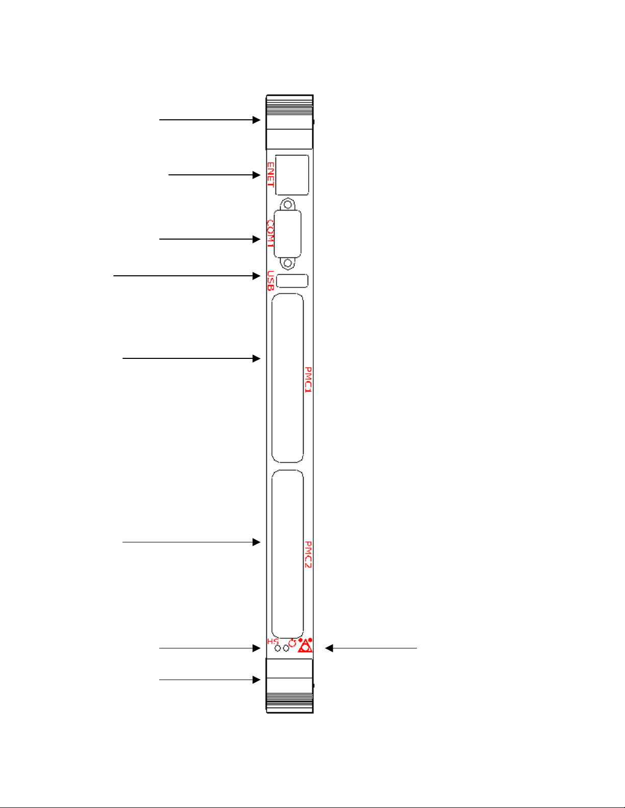
CPB-4612 Faceplate
Ejector Handle
10/100 Ethernet
COM RS-232
Serial Port
USB
PMC
PMC
Hotswap LED
Reset Switch
Ejector Handle
3
Page 14

1.2 Features
There are two SKU's of the cPB-4612. The first is the cPB-4612, which has a 64bit/66Mhz PMC site and a
32bit/33Mhz PMC site. . The second is the cPB-4612 w/ IDE, which has a 64bit/66Mhz PMC site and an
on-board 2.5” HDD IDE connector. Other features include:
• CompactPCI Specification, PICMG 2.0, Version 2.1** compliant
• CompactPCI Specification, PICMG 2.16, Version 1.0** compliant
• 6U single-slot CompactPCI form factor
• Mobile Intel Pentium M, micro FCBGA package
• Intel
• Integrated Intel Extreme Graphics 2 controller
• Dual 10/100/1000 Mb/s Ethernet (both at the J3 backplane connector to support PICMG 2.16)
• 10/100 Mb/s Ethernet (available at the front panel)
• 1 MB of Level 2 cache
• 400 MHz front side bus
• Socketed 256 MB, 512 MB, 1 GB, or 2GB of DDR SDRAM memory at 200, 266, or 333 MHz
• Dual stage watchdog timer
• IPMI support
• Option for either a single on-board PCI Mezzanine Card (PMC) slot (32-bit / 33MHz) or a primary IDE
• 64bit / 66Mhz @ 3.3V PCI Mezzanine Card (PMC) slot
• Two 16C550 RS-232 serial ports (COM1 available at the faceplate, COM2 available through the J5
• Push Button Reset on the front panel
• 1 USB on front panel, 2 USB ports available via RTM
• Rear-Panel I/O Availability (at J5) includes the following:
• Support for Microsoft Windows 2000/XP, Red Hat Linux, and Solaris 8/9
• Standard AT* Systems include:
®
855GME GMCH and 6300ESB ICH
channel that supports an on-board 2.5 inch hard disk
backplane connector)
– Secondary IDE channel
– Serial ATA
– Two USB ports
– VGA video
– Serial Port
– Two enhanced interrupt controllers (8259)
– Three counter/timers (one 8254)
– Real-time clock/CMOS RAM (146818B)
– Two enhanced DMA controllers (8237)
1.3 Functional Blocks
The following topics provide overviews of the cPB-4612's main features, some of which are shown in the
functional block diagram below.
4
Page 15
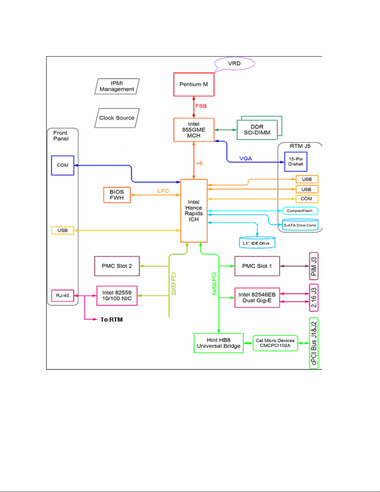
Functional Block Diagram
1.3.1 CompactPCI/PSB Architecture
The cPB-4612 is designed to operate in a PICMG 2.0 CompactPCI backplane. If the system is placed in a
system slot, the bridge will automatically configure itself as a transparent bridge, and the board will perform
as the host. If the board is placed in a peripheral slot, the bridge will automatically configure itself as a nontransparent bridge, and the board will perform as a peripheral device.
When used in accordance with the CompactPCI Packet Switching Backplane Specification, PICMG 2.16,
Version 1.0, the cPB-4612 functions as a "Dual Link Port Node" board. The cPB-4612 can be connected to a
5
Page 16

system's fabric-switched Link Ports A and B, and can be inserted into system or peripheral slots. The cPB4612 is keyed for insertion into compatible slots.
The "CompactPCI" topic in Appendix D contains a link to the PCI Industrial Computer Manufacturers Group.
1.3.2 Processor
The cPB-4612 uses the Mobile Pentium M in a micro FCBGA package. The 1MB or 2MB on-die transfer L2
cache is integrated with the CPU, eliminating the need for separate components and improving
performance. The FCBGA package Pentium M processor also operates with a 400 MHz Processor Side
Bus for very fast access to memory and data.
The "Mobile Pentium M (FCBGA Package)" topic in Appendix D contains a link to the datasheet for the
processor.
1.3.3 Chipset
The Intel 855GME chipset consists of two controller hubs. The 855GME Memory Controller Hub (MCH)
supports a 400MHz system bus, DDR200/266/333 memory, and an integrated graphics solution w/Intel
Extreme Graphics 2 technology. The 6300ESB I/O Controller Hub (ICH4) makes a direct connection to the
memory for faster access to peripherals. It provides the features and bandwidth required for applied
computing-usage models. The following is a list of features of the 855GME chipset:
• Designed, validated, and optimized for the Intel Pentium M with NetBurst™ micro-architecture
using proven and established building blocks
• 400MHz system bus delivers a high-bandwidth connection between the Intel Pentium M and the
platform, providing 3x the bandwidth over platforms based on Intel® Pentium® III processors
• USB controllers provide high performance peripherals with 480Mbps of bandwidth. This results
in a significant increase over previous integrated 1-4 port hubs at 12Mbps
• Dual UARTs
• Serial ATA
• 64bit/66Mhz PCI-X bus
• 32bit/33Mhz PCI bus
®
• Dual Ultra ATA/100 controllers, coupled with the Intel
software package - support faster IDE transfers to storage devices
• The Intel® Application Accelerator software provides additional performance over native ATA
drivers. The Intel Application Accelerator improves system performance by improving I/O
transfer rates and enables faster O/S load time resulting in accelerated boot times
• Embedded lifecycle support
The "Intel 855GME Chipset" topic in Appendix D contains a link to information about the chipset.
Application Accelerator - a performance
1.3.4 PCI-to-PCI Bridge
The cPB-4612 has a 64bit/66Mhz PCI-X bridge to the CompactPCI backplane. The bridge will configure
itself as a transparent bridge when the board is in a system slot, so that the cPB-4612 can be the system
host. If the cPB-4612 is placed in a peripheral slot, the bridge configures itself as a non-transparent bridge,
and will show up as a PCI device to the host. This allows use of the board in either a system or peripheral
slot.
6
Page 17

1.3.5 Memory and I/O Addressing
The cPB-4612 supports up to 2GB of DDR333/266/200 via two right-angled SODIMM sockets. Memory
can be purchased from DTI separately.
See the "Memory Configuration" and "I/O Configuration" topics in Chapter 2 for more information.
1.3.6 Power Ramp Circuitry
The cPB-4612 features a power controller with power ramp circuitry that allows the board's voltages to be
ramped in a controlled fashion. The power ramp circuitry eliminates large voltage or current spikes caused
by hot swapping boards. This controlled ramping is a requirement of the CompactPCI Hot Swap
Specification**, PICMG 2.1, Version 1.0.
The cPB-4612's power controller unconditionally resets the board when it detects that the 3.3V, 5V, and 12V
supplies are below an acceptable operating limit. Minimum voltage thresholds for the cPB-4612 are: 4.75V
(5V supply), 3.0V (3.3V supply), and 10.0V (+12V supply).
1.3.7 Rear-Panel I/O
The following I/O signals are available from the J5 connector at the back of the cPB-4612. These signals are
available for use by a rear panel transition board such as the cRT-4612.
• Serial port (COM2)
• USB Ports 2 and 3
• Secondary IDE channel
• Serial ATA channel
• Video
1.3.8 Video
The cPB-4612 supports VGA video using Intel’s 855GME video interface. The video is accessed through
the CompactPCI J5 connector. The 855GME can share up to 32MB of system memory with the internal
video.
The onboard video from the Intel 855GME may be disabled by a jumper setting. This will allow use of a PCI
video card only. If the onboard video is enabled and a PCI video card is installed, the PCI video card will be
the primary video source.
The Intel 855GME Chipset topic contains a link to the datasheet for this device.
1.3.9 PCI Mezzanine Card (PMC) Interface
The cPB-4612 provides a 64bit/66Mhz PMC site and a 32bit/33Mhz PMC site, both with front panel access.
The 64bit/66Mhz PMC site is only 3.3V tolerant. The 32bit/33Mhz can be configured to be either 3.3V or 5V
via a jumper setting. Voltage keys are also provided to prevent inadvertently placing a PMC card on PMC
site that does not support its VI/O voltage.
The cPB-4612 w/ IDE provides a 64bit/66Mhz PMC site and a 2.5” HDD IDE connector. The 64bit/66Mhz
PMC site is only 3.3V tolerant. Voltage keys are also provided to prevent inadvertently placing a PMC card
on PMC site that does not support its VI/O voltage.
The "PMC Specification" topic in Appendix D contains a link to the sponsoring organization for the PMC
specification.
1.3.10 Dual 10/100/1000 Ethernet Interfaces
The cPB-4612 provides two 10/100/1000BaseTx Ethernet channels (ENET A and ENET B) through the
Intel 82546EB Fast Gigabit Ethernet Multifunction PCI Controller. The 82546EB consists of both the Media
7
Page 18

Access Controller (MAC) and the physical layer (PHY) interface combined into a single component solution.
Both Ethernet Channels are directed to the rear connector at J3 for PICMG 2.16 support.
The "Ethernet
cPB-4612.
" topic in Appendix D contains links to the datasheets for the Ethernet devices used on the
1.3.11 10/100 Ethernet Interface
The cPB-4612 supports one 10/100 Base-TX Ethernet interface. The Intel 82559EM Ethernet controller
provides this interface. The NIC address programmed into the controller is located on labels on the board.
Link and activity LED signals are on the front panel at the RJ-45 connector.
The "Ethernet
cPB-4612.
" topic in Appendix D contains links to the datasheets for the Ethernet devices used on the
1.3.12 IDE Hard Drive
The cPB-4612 w/IDE supports an onboard ATA/100 2.5” IDE interface. This can be used to connect a 2.5”
hard drive. The IDE interface is implemented using Intel’s 6300ESB I/O Controller Hub (ICH). Note that the
onboard 2.5” IDE connector is not present on versions of the board that support the 33MHz/32 bit PMC site.
All versions of the cPB-4612 supports a second ATA/100 IDE interface through the CompactPCI J5
connector. The IDE interface is implemented using Intel’s 6300ESB I/O Controller Hub (ICH).
All versions of the cPB-4612 supports a Serial ATA/150 interface through the CompactPCI J5 connector.
The IDE interface is implemented using Intel’s 6300ESB I/O Controller Hub (ICH).
Both the 2.5” IDE drive connector and 33Mhz/32bit PMC site cannot both be present at the same time, since
they are in the same physical space on the board. Which one is populated depends on the version of the
board.
See Chapter 6, "IDE Controller", for more information.
1.3.13 Serial I/O
The cPB-4612 provides support for two RS-232 compatible serial ports. COM1 is accessible at the
faceplate through a 9-pin DSUB connector. This port is typically used for test access. COM2 is available at
the J5 Rear Panel I/O connector.
The serial port interface is implemented using Intel’s 6300ESB I/O Controller Hub (ICH).
1.3.14 Interrupts
Two enhanced, 8259-style interrupt controllers provide the cPB-4612 with a total of 15 interrupt inputs.
Interrupt controller features include support for:
• Level-triggered and edge-triggered inputs
• Individual input masking
• Fixed and rotating priorities
Interrupt sources include:
• Counter/Timers
• Serial I/O
• Keyboard
• Floppy disk
• IDE interface
8
Page 19

• Real-Time Clock
• On-board PCI devices
Enhanced capabilities include the ability to configure each interrupt level for active high-going edge or active
low-level inputs.
The cPB-4612's interrupt controllers reside in the 6300ESB device. The "Intel 855GME Chipset" topic in
Appendix D provides a link to the datasheet for this device.
1.3.15 Counter/Timers
Three 8254-style counter/timers, as defined for the PC/AT, are included on the cPB-4612. Operating modes
supported by the counter/timers include:
• Interrupt on count
• Frequency divider
• Software triggered
• Hardware triggered
• One shot
The cPB-4612's Counter/Timers reside in the Intel 6300ESB device. The "Intel 855GME Chipset" topic in
Appendix D provides a link to the datasheet for this device.
1.3.16 DMA
Two cascaded 8237-style DMA controllers are provided on the cPB-4612 for use by the on-board
peripherals.
The cPB-4612's DMA controllers reside in the Intel 6300ESB device. The "Intel 855GME Chipset" topic in
Appendix D provides a link to the datasheet for this device.
1.3.17 Real-Time Clock
The real-time clock performs timekeeping functions and includes 256 bytes of general-purpose, batterybacked, CMOS RAM. Timekeeping features include an alarm function, a maskable periodic interrupt, and a
100-year calendar. The system BIOS uses a portion of this RAM for BIOS setup information.
The cPB-4612's Real-Time Clock resides in the Intel 6300ESB device. The "Intel 855GME Chipset" topic in
Appendix D provides a link to the datasheet for this device.
1.3.18 Reset
The push-button reset on the cPB-4612's faceplate functions as a "Hard Reset". See Chapter 4, "Reset," for
more information about reset sources for the cPB-4612.
1.3.19 Two-Stage Watchdog Timer
The watchdog timer optionally monitors system operation and is programmable for different timeout periods
(from 1 microsecond to 10 minutes). It is a two-stage watchdog, meaning that it can be enabled to produce a
system management interrupt (SMI) or an IRQ (APIC 1, INT 10) before it generates a Reset. Failure to
strobe the watchdog timer within the programmed time period may result in an SMI, a reset request, or both.
A register bit can be read to indicate if the watchdog timer caused the reset event. This watchdog timer
register is not cleared on power-up, enabling system software to take appropriate action if the watchdog
generated the reboot.
See Chapter 7, "Watchdog Timer," for more information, including sample code.
9
Page 20

1.3.20 Universal Serial Bus (USB)
The Universal Serial Bus (USB) provides a common interface to slower-speed peripherals. Functions such
as keyboard, serial ports, printer port, and mouse ports can be consolidated into USB, simplifying cabling
requirements. The cPB-4612 provides one USB port at its faceplate (connector J20 is Port 0). USB Port 1
and USB port 2 are routed to the cPB-4612’s J5 Rear Panel I/O connector.
The cPB-4612’s USB channels are controlled by the Intel 6300ESB device. The "Intel 855GME Chipset"
topic in Appendix D provides a link to the datasheet for this device.
1.3.21 System Environmental Monitor
This board provides an IMPI controller for monitoring the status of the system environment. The IPMI
controller monitors the system voltages, ambient board temperature, and CPU temperature. The controller
is accessed through an IPMB bus from the backplane.
See "System Monitoring and Control" in chapter 5 for more details.
1.3.22 LED Indicators
The LEDs located at the cPB-4612’s faceplate are defined below.
• Ethernet (ENETA, RJ 45 connector):
First LED:
Green = Network connection
Blinking Green = Network activity
Second LED:
Off = 10 MB/sec
Green = 100 MB
• Hot Swap
Blue = safe to extract board
Off = not safe to extract board
1.4 Software
The cPB-4612 includes a DTI enhanced AMI Embedded BIOS loaded in on-board flash. The BIOS is userconfigurable and can boot an operating system from CompactFlash, a hard drive, CD-ROM drive, or over a
network. BIOS and firmware updates can be provided by DTI.
The cPB-4612 is compatible with all major PC operating systems, including Microsoft* Windows* 2000/XP,
Linux*, and VxWorks*. Chips may provide additional drivers for Intel peripherals, flash drives, and for
supported operating systems. Software device drivers for the cPB-4612 may be found on the DTI Product
Documentation and Software CD.
10
Page 21

Chapter
2 Getting Started
This chapter summarizes the information needed to make the cPB-4612 operational. This chapter should be
read before using the board.
2
2
11
Page 22

2.1 Unpacking
Check the shipping carton for damage. If the shipping carton and contents are damaged, notify the carrier
and DTI for an insurance settlement. Retain the shipping carton and packing material for inspection by
the carrier. Obtain authorization before returning any product to DTI. Refer to the Return Shipment
Information page for assistance.
CAUTION: This board must be protected from static discharge and physical shock. Never
remove any of the socketed parts except at a static-free workstation. Use the anti-static bag
shipped with the product to handle the board. Wear a wrist strap grounded through one of
the system's ESD Ground jacks when servicing system components.
2.2 System Requirements
The following topics briefly describe the basic system requirements and configurable features of the cPB-
4612. Links are provided to other chapters and appendices containing more detailed information.
2.2.1 BIOS Version
For proper operation, the cPB-4612 must run the DTI enhanced AMI Embedded BIOS. The revision level
is shown in the BIOS Identification string displayed during the Power On Self Test (POST).
2.2.2 Connectivity
The cPB-4612 features an ejector handle that is keyed for compatible slots. The board can only be
inserted into slots fitted with a compatible mating key.
The cPB-4612 is designed to operate in a backplane providing CompactPCI form factor interfaces at J1,
J2, J3, and J5. The J1 and J2 connectors are supplied for the CompactPCI bus, power and IPMI signals.
J3 signaling must comply with the PICMG* 2.16 Packet Switching Backplane specification. The J5
interface must have through-pins for the cPB-4612 to interface with a rear panel transition card such as
the cRT-4612. See the "Connectors" topic in Appendix B for connector descriptions.
2.2.3 Electrical and Environmental
The cPB-4612 meets the following requirements:
• +5VDC +5%, -3% @ 6.9A typical
• +3.3VDC +5%, -3% @ 2.4A typical
• +12VDC ±10% @ 20mA typical
• -12VDC may be required by a PMC peripheral installed on the cPB-4612.
12
Page 23

Configuration 5V
(avg)
5V
(peak)
3.3V
(avg)
3.3V
(peak)
12V
(avg)
12V
(peak)
-12V
(avg)
-12V
(peak)
1.7GHz / 512MB 6.9A TBD* 2.4A TBD* 20mA 50mA 0.0A 0.0A
Hard disk (add)
540mA 1.00A N/A N/A N/A N/A N/A N/A
(typical)
PMC card typical1
1.00A 1.70A 0.75A 1.30A 100mA 200mA 20mA 40mA
(add)
PMC card max.
2
1.50A 3.00A 2.25A 4.50A 500mA 500mA 500mA 500mA
(add)
* Peak (short duration) power supply current may be significantly higher (up to 50%) and will
vary depending upon the application.
Notes:
1. Consult manufacturer of installed PMC card for actual values.
2. In no case shall the total power dissipated by the PMC card exceed 10.0 W.
The cPB-4612 comes with a heatsink that allows the processor to operate between 0° and approximately
50°C ambient with a minimum of 200 LFM (1 meter per second) of external airflow. It is the users'
responsibility to ensure that the cPB-4612 is installed in a chassis capable of supplying adequate airflow.
The maximum power dissipation of the processor (FCBGA package) is 25W. External airflow must be
provided at all times. See Appendix A, "Specifications," and Appendix C, "Thermal Considerations," for
more details.
It is strongly recommended that the airflow be measured while the cPB-4612 is installed in its intended
location. Insert a thermistor type air velocity meter (Kane-May KM4007 or similar) through the PMC
access on the faceplate and make the air velocity measurement near the processor heat sink. Power
should not be applied to the cPB-4612 during airflow measurements (slightly disengage the cPB-4612
from the backplane connectors if necessary).
CAUTION: The processor "core" temperature must never exceed 100°C under any condition
of ambient temperature or usage. This may result in permanent damage to the processor.
The cPB-4612 may contain materials that require regulation upon disposal. Please dispose of this product
in accordance with local rules and regulations. For disposal or recycling information, please contact your
local authorities or the Electronic Industries Alliance at http://www.eiae.org/**.
2.3 Memory Configuration
The cPB-4612 components can address up to 4 GB of memory, but the board only has two SO-DIMM
sockets and can physically only hold two sticks of memory. The address space is divided between
memory local to the board and memory located on the Local PCI bus. Any memory not reserved or
occupied by a local memory device (DRAM/flash) is available to PCI memory devices.
The cPB-4612 can support up to two sticks of either 256 MB, 512 MB, 1 GB DDR SDRAM. 1MB of
L2 cache is integrated with the Pentium
®
–M processor.
13
Page 24

Memory Address Map Example
FFF80000h - FFFFFFFFh SYSTEM BIOS/Flash
8000000h - FFF7FFFFh PCI PERIPHERALS
4 GB
4 GB - 512 KB
100000h - 1FFFFFFFh SYSTEM MEMORY
E0000h - FFFFFh SYSTEM BIOS
C8000h - DFFFFh BIOS EXTENSION
C0000h - C7FFFh
A0000h - BFFFFh
0h - 9FFFFh LOCAL DRAM
VGA BIOS
VGA DISPLAY
MEMORY
512 MB
1 MB
896 KB
800 KB
768 KB
640 KB
0
14
Page 25

2.4 I/O Configuration
The cPB-4612 addresses up to 64 KB of I/O using a 16-bit I/O address. The cPB-4612 is populated with
many commonly used I/O peripheral devices. The I/O address location for each peripheral is shown in the
"I/O Address Map" illustration.
I/O Address Map
D00 - FFFFh PCI*
*Onboard ISA peripherals
addressed between
100h - 7FFh decode 11 bits
of address (A0h - A10h).
Therefore, these peripherals
will alias throughout the 16-bit
I/O space at the following
ranges:
x100-x3FFh
x500-x7FFh
x900-xBFFh
xD00-xFFFh
PCI devices can fully utilize
the address space from
D00 - FFFFh, since subtractive
decoding is used for the
onboard ISA devices.
CF8 - CFFh PCI Config/RST Control
780 - CF7h PCI Reserved
778 - 77Fh LPT ECP Registers
400 - 777h
3F8 - 3FFh COM1
3F0 - 3F7h Floppy / IDE Registers
3E0 - 3EFh
3B0 - 3DFh VGA Registers
380 - 3AFh
378 - 37Fh LPT
300 - 377h
2F8 - 2FFh COM2
200 - 2F7h
1F8 - 1FFh
1F0 - 1F7h Primary IDE Registers
178 - 1DFh
170 - 177h Secondary IDE Registers
100 - 16Fh
F0 - FFh Coprocessor
E0 - EFh
C0 - DFh On-board Slave DMA Controller
B4 - BFh
B2 - B3h APM Registers
B0 - B1h
A0 - AFh On-board Slave Interrupt Controller
93 - 9Fh
92h Fast RESET and Gate A20
90 - 91h
81 - 8Fh On-board DMA Page Registers
Reserved
Reserved
Reserved
Reserved
Reserved
Reserved
Reserved
Reserved
Reserved
Reserved
Reserved
Reserved
Reserved
15
Page 26

0 - 1Fh On-board Master DMA Controller
80h Diagnostic Port
78 - 79h Reserved
70 - 77h On-board Real-Time Clock
60 - 6Fh Keyboard and System Ports
50 - 5Fh
40 - 4Fh On-board Timer/Counters
30 - 3Fh
2E - 2Fh Super I/O Configuration
22 - 2Dh
20 - 21h On-board master Interrupt Controller
Reserved
Reserved
Reserved
2.5 Connectors
The cPB-4612 includes several connectors to interface to application-specific devices. Refer to the
"Connectors" topic in Appendix B for complete connector descriptions and pin outs.
2.6 Jumper Options
The cPB-4612 provides several jumper configuration options for features that cannot be provided through
the BIOS Setup Utility. Location figures and descriptions are provided in Chapter 3, "Configuration."
2.7 BIOS Configuration Overview
This topic presents an introduction to the cPB-4612’s BIOS.
The BIOS has many separately configurable features. These features are selected by running the built-in
Setup utility. System configuration settings are saved in a portion of battery-backed RAM in the real-time
clock device and are used by the BIOS to initialize the system at boot-up or reset. The configuration is
protected by a checksum word for system integrity.
To access the Setup utility, press F2 during the system RAM check at boot-up. When Setup runs, an
interactive configuration screen displays. Refer to the following "Setup Screen" illustration for an example.
Setup parameters are divided into different categories. The available categories are listed in a menu
down the left side of the setup screen. The parameters within the highlighted (current) category are listed
in the main (right) portion of the Setup screen. Context sensitive help can be displayed for each
parameter by highlighting the parameter and pressing F1. A legend of keys is listed at the bottom of the
Setup screen.
Use the up and down arrow keys to select a category from the menu. Use the up and down arrow keys to
select a parameter in the main portion of the screen. Use the +/– or ↔keys to change the value of a
parameter.
Solid arrows next to menu items in the main screen indicate submenus. To display a submenu, use the
up and down arrow keys to highlight the submenu and then press Enter.
16
Page 27

Setup Screen
SYSTEM CONFIGURATION SUMMARY
SYSTEM SUMMARY
SYSTEM SETUP
HARD DISK SETUP
BOOT ORDER
PERIPHERALS
USB CONFIG
MISC. CONFIG
EVENT LOGGING
SECURITY/VIRUS
Diversified Technology, Inc – cPB4612
CPU Type :Intel(R) Pentium(R) M processor 1700MHz
CPU Speed : 1.70GHz Hard Disk 0: Not Detected
L2Cache : 1024KB Hard Disk 1: Not Detected
Base RAM : 639K Hard Disk 2: Not Detected
Extended RAM: 480MB Hard Disk 3: Not Detected
Video RAM : 32MB COM Ports : 3F8 2F8 3E8
PCB Revision: 1.0 BIOS Date : 03/31/04
Memory Mode : PC2100 (266MHz) DDR SDRAM with ECC
PMC Slot 1 : PCI-X 66 MHz
PMC Slot 2 : PCI 33 MHz
USB Devices : 1 Keyboard, 1 Mouse, 1 Hub, 1 Drive
↑↓ Select Screen Enter Go to Sub Screen
F1 General Help Esc Exit
EXIT
Copyright (c) 2004, Diversified Technology, Incorporated
2.8 Operating System Installation
For more detailed information about your operating system, refer to the documentation provided by the
operating system vendor.
1. Install peripheral devices. CompactPCI* devices are automatically configured by the BIOS during
the boot sequence.
2. Most operating systems require initial installation on a hard drive from a floppy or CD-ROM drive.
These devices should be configured, installed, and tested with the supplied drivers before
attempting to load the new operating system.
3. Read the release notes and installation documentation provided by the operating system vendor.
Be sure to read any README files or documents provided on the distribution disks, as these
typically note documentation discrepancies or compatibility problems.
4. Select the appropriate boot device order in the SETUP boot menu depending on the OS
installation media used. For example, if the OS includes a bootable installation floppy, select
Removable Media as the first boot device and reboot the system with the installation floppy
installed in the floppy drive. (Note that if the installation requires a non-bootable CD-ROM, it is
necessary to boot an OS with the proper CD-ROM drivers in order to access the CD-ROM drive).
17
Page 28

5. Proceed with the OS installation as directed, being sure to select appropriate device types if
prompted. Refer to the appropriate hardware manuals for specific device types and compatibility
modes of DTI products.
6. When installation is complete, reboot the system and set the boot device order in the SETUP
boot menu appropriately.
18
Page 29

Chapter
3 Configuration
The cPB-4612 has been designed for maximum flexibility. Many features can be configured by the user
for specific applications. Most configuration options are selected through the BIOS Setup utility
(discussed in the "BIOS Configuration Overview" topic in Chapter 2). Some options cannot be software
controlled and are configured with jumpers.
3
3
19
Page 30

Jumper Options and Locations
The cPB-4612 contains a push-button switch on the faceplate and eight jumpers on the component side
of the board. The jumpers are listed and briefly described in the "Jumper Cross-Reference" table below.
Factory default switch settings are shown in the "Default Jumper Settings" figure.
Jumper Cross-Reference Table
Jumper Function
PB1 Reset (push-button on faceplate)
J16-1 BKT-GND to GND
J16-2 +12V to J5-pin D1
J16-3 +5V PMC I/O
J16-4 IMPI Disable
J17-1 Not Used
J17-2 CMOS Clear
J17-3 Disable Onboard Video
J17-4 Manufacture Test Mode
20
Page 31

Default Jumper Configuration
3.1 Switch Descriptions
The following topics list the switches in numerical order and provide a detailed description of each switch.
3.1.1 PB1 (Reset)
PB1 is a push-button on the front of the cPB-4612. Pressing PB1 issues a hard reset. Reset is discussed
in more detail in Chapter 4.
3.1.2 J16-1 (BKT-GND to GND)
Installing this jumper will short the bracket ground to digital ground. This may positively or negatively
affect EMI emissions, depending on the system. Proper testing would need to be performed with the
intended system to determine the best setting. The default is for no jumper.
J16-1 Function
Open Default Bracket ground is not connected to digital ground.
Closed Bracket ground is shorted to digital ground.
21
Page 32

3.1.3 J16-2 (+12V to J5-pin D1).
Installing this jumper will connect +12V to the CompactPCI connector J5, pin D1. This is only to be used
for specially designed RTM cards that may need it. The default is for no jumper.
J16-2 Function
Open Default CPCI J5-pin D1 is a no connect.
Closed CPCI J5-pin D1 is shorted to +12V.
3.1.4 J16-3 (+5V PMC I/O)
Installing this jumper sets the 32bit/33Mhz PMC site’s VI/O voltage to +5V. Having no jumper sets the
VI/O voltage to 3.3V. The 32bit/33Mhz PMC site is located on the bottom edge of the board, closest to
the jumpers.
WARNING: The voltage key for the 32bit/33Mhz PMC site must be set to match this jumper setting.
Not placing the voltage key, placing the voltage key at the wrong location, or using a PMC card that is not
tolerant of the set voltage may damage the PMC card and/or the cPB-4612 board.
J16-3 CMOS Real Time Clock
Open Default 32bit/33Mhz PMC site set to 3.3V.
Closed 32/bit/33Mhz PMC site set to 5V.
3.1.5 J16-4 (IMPI Disable)
This is for debug use only. Placing this jumper will disable the IMPI controller. This should only be used
by the manufacturer.
J16-4 CMOS Real Time Clock
Open Default Normal Operation
Closed IMPI controller disabled
3.1.6
Not used
J17-1 (Not Used)
J17-1 Function
Open Default Not used
Closed Not used
3.1.7 J17-2 (CMOS Clear)
Installing this jumper will reset the CMOS settings to their default values.
J17-2 Function
Open Default Normal operation
Closed Clears CMOS and sets registers to their default state.
22
Page 33

3.1.8 J17-3 (Disable Onboard Video)
Installing this jumper will disable the onboard video. Place this jumper if using a PCI video card only.
J17-3 Function
Open Default Onboard video is enabled.
Closed The onboard video is disabled.
3.1.9 J17-4 (Manufacture Test Mode)
Used by DTI for testing purposes. Do not install a jumper at this location.
J17-4 Function
Open Default Normal operation
Closed Board in manufacturing test mode.
3.1.10 J18 (Ejector Switch)
The ejector handles are used when cPB-4612 is inserted or removed (hot swapped) from a chassis that is
powered on. When a customer wishes to remove a board from a system that is powered on then the
ejector handles should be opened just enough to disengage the handles from the chassis, but without
fully disengaging the J-connectors from the back of the chassis. This will trigger a shutdown of the
operating system and then the BMC will power off the board and light the blue hot swap LED on the front
panel. Once the blue LED on the front of the board is lit, then it is safe to remove the board from the
chassis.
Note: In order for the shutdown sequence of the OS to take place a hot swap driver must be
installed into the OS. See the cPB-4612 support page for this driver or procure the cPB-4612
hot swap kit.
The J18 (ejector handles) need to be closed in order for the board to boot up.
J18 Function
Open Indicate the user needs to extract the board
Closed Normal Operation
23
Page 34

Chapter
4 Reset
This chapter discusses the reset types and reset sources on the cPB-4612. If necessary, the cPB-4612’s
board reset characteristics can be tailored to the requirements of a specific system.
4
4
24
Page 35

4.1 Reset Types and Sources
The cPB-4612’s reset types are listed below. The sources for each reset type are detailed in the following
topics.
• Hard Reset: All devices are held in reset.
• Soft Reset: CPU initialization only. Other devices are not reset.
• Backend Power Down: The backend logic is powered off. The board is powered on and is held in
reset.
• NMI: Non-maskable interrupt. Though not a reset in the strict sense, an NMI can have the same
effect as other resets.
4.1.1 Hard Reset Sources
System Register CF9h (6300ESB Reset Control Register)
Bits 1 and 2 in this register are used by the 6300ESB to generate a hard reset or a soft reset. During a
hard reset, the 6300ESB asserts CPURST, PCIRST#, and RSTDRV. Additionally, it resets its core and
suspends well logic.
4.1.2 Soft Reset Sources
System Register CF9h (6300ESB Reset Control Register)
Bits 1 and 2 in this register are used by the 6300ESB to generate a hard reset or a soft reset. During a
soft reset, the ICH4 asserts INIT to the CPU for 16 PCICLK. This causes the processor to enter "real
mode", initialize its internal registers, and begin instruction execution from FFFFFFF0h (the boot vector).
Keyboard Controller Reset
The keyboard controller generates a keyboard controller reset when FEh is written to port 64h. This
causes the 6300ESB to assert INIT to the CPU.
Keyboard CTRL-ALT-DEL
Simultaneously pressing these keys calls a BIOS function that reboots the system.
Note: This method does not work under operating systems that trap calls to this BIOS
function.
Watchdog Timer (System Register Address 79h)
The watchdog timer may be programmed to generate a "CPU Init" if it is not strobed within a given timeout period. This function is discussed in Chapter 7, "Watchdog Timer."
4.1.3 Backend Power Down Sources
Board Extraction
When a board is extracted from an enclosure (specifically, when the "board-select" [BD_SEL] pin is
disengaged), the hot swap controller unconditionally removes backend power from the board and holds
the board in reset.
Low Voltage
When any of the 3.3V, 5V, or 12V supply voltages are detected to be below an acceptable operating limit,
the hot swap controller unconditionally removes backend power and holds the board in reset.
25
Page 36

4.1.4 NMI Sources
Watchdog Timer (System Register Address 79h)
The watchdog timer may be programmed to generate a non-maskable interrupt if it is not strobed within a
given time-out period. This function is discussed in Chapter 7, "Watchdog Timer."
26
Page 37

Chapter
5 System Monitoring and Control
The cPB4612 has an IPMI System Monitor that complies with PICMG® 2.9 specification, and complies
with IPMI Specification 1.5. This allows a PICMG 2.9 compliant chassis that utilizes a chassis manager,
or Baseboard Management Controller (BMC) to detect the presence of the cPB4612 and make Field
Replaceable Unit (FRU) information, and Sensor Device Records (SDR’s) available. Sensors monitor
voltages, CPU and system temperature, and other inputs, including the front latch, which can generate
events that are recorded in the BMC’s System Event Log (SEL). The IPMI System Monitor has both an
IPMB and a dedicated basic serial interface, so that it is possible for the cPB4612 to acquire FRU and
sensor information directly from the IPMI System Monitor. The firmware on the IPMI System Monitor can
be upgraded via the serial interface or over IPMB.
5
5
27
Page 38

5.1 Monitoring and Control Functions
The IPMI System Monitor has a dedicated serial interface to the host processor on the cPB4612. It is a
16550-compatible UART that is configurable in SETUP. If this interface is not required, it can be
disabled. Otherwise, it will be given a unique serial port address and interrupt. Note that the interrupt
cannot coincide with the other COM ports; it is not shareable.
The serial interface is fixed at 9600 baud, 8 data bits, 1 stop bit, no parity, full duplex. It complies with
IPMI serial “basic” mode, as detailed in IPMI Spec 1.5, section 13.4, which permits IPMB packets to be
transmitted and received using framing bytes and escape sequences. The packet structure otherwise is
identical to the IPMB:
Figure 5.1: Packet Structure
Because the serial interface in this case is dedicated, the responder address and requester address bytes
can be anything. The IPMI System Monitor, though, will always put its actual IPMB slave address in the
rsAddr field of a response packet.
The IPMI 1.5 specification defines a basic mode serial port as a single session interface, since there is no
session ID in the packet. This IPMI System Monitor, at this time, does not support Get Session Challenge
and Activate Session commands, because the serial interface is dedicated to the IPMI system monitor,
and the interface is always “up.”
5.2 IPMB
The IPMB is an I2C® interface that is routed through the backplane and connects to the BMC in the
chassis to allow discovery of the IPMI System Monitor. Its operation is covered in the IPMI specification.
It is always active.
28
Page 39

5.3 Field Replaceable Unit (FRU) Information
Board information, such as serial number, date of manufacture, OEM name, part number, etc., are
retrievable from the FRU. It complies with the IPMI FRU 1.0 Specification. The information in the FRU
can be customized to add other product information, such as asset tag, other part numbers, etc.
5.4 Sensors
The sensors that the cPB4612 supports with the IPMI System Monitor can be retrieved in the Sensor
Data Records (SDR’s) via normal IPMI commands. They include:
System Ambient Temperature +12V
CPU Temperature +1.5V
VTT DDR +1.8V
CPU Core Voltage ONCTL#
+3.3V SLOT
+5V Front Latch
These sensors (with the exception of ONCTL and SLOT), when enabled by the BMC, will generate
sensor events on the IPMB. These events will normally be logged by the BMC and time-date stamped.
On temperature and voltage sensors, if sensor readings cross any of the non-critical, critical, or nonrecoverable thresholds, the IPMI System Monitor will generate IPMB event data to inform the BMC. The
IPMI System Monitor allows the BMC, via IPMI commands, to override its sensor thresholds
5.5 Firmware Updates
Firmware updates are possible through either the serial or IPMB interface. A special utility will be
provided should a firmware update be necessary.
5.6 SMBus Address Map
The table below lists the location, function, and address of each SMBus device used on the cPB-4612.
Device cPB-4612 Function Address
ICH SMBus
(slave)
Board clock
generator
(CK409B)
6300ESB ICH 1000 100
Board clock generator (CK409B) 1101 001
SO-DIMM0 SO-DIMM0 1010 000
SO-DIMM1 SO-DIMM1 1010 001
29
Page 40

Chapter
6 IDE Controller
The cPB-4612 with IDE has an on-board IDE controller that provides two IDE channels for interfacing with
up to four IDE devices. The IDE controller is incorporated into the Intel 6300ESB, which supports ATA-
100. There is one 50-pin IDE connector on the cPB-4612 with IDE, which supports up to two IDE devices
(though there is only space on the board itself to mount one device). The secondary IDE channel is
available through the rear panel connector (J5).
The "Intel 855GME Chipset" topic in Appendix D provides a link to the 6300ESB datasheet.
6
6
30
Page 41

6.1 Features of the IDE Controller
• Primary and Secondary channels for interfacing up to four devices
• IBM-AT compatible
• Supports PIO and Bus Master IDE
• "Ultra ATA/33/66/100" Synchronous DMA Operation
• Bus Master IDE transfers up to 100 MB/sec.
• Individual software control for each IDE channel
6.2 Disk Drive Support
The cPB-4612 supports internal and external IDE devices. These configurations are described below.
6.2.1 Primary IDE Channel
The cPB-4612’s primary IDE channel is directed to the J14 IDE connector. J14 is used to interface with
the locally mounted hard drive.
6.2.2 Secondary IDE Channel
The cPB-4612’s Secondary IDE channel is directed via the J5 rear-panel I/O connector to a compatible
rear panel I/O board. Rear Panel I/O boards, such as the cRT-4612, can be installed in-line behind the
cPB-4612 to provide expanded I/O capability. Refer to the DTI PlexSys cRT-4612 Packet Switched RearPanel Transition Board Hardware Manual for product information.
6.3 IDE I/O Mapping
The I/O map for the IDE interface varies depending on the mode of operation. The default mode is
"compatibility mode," meaning that the interface uses the PC-AT legacy addresses of 1F0h-1F7h, with
3F6h and interrupt IRQ14 for the primary channel. The secondary channel uses I/O addresses 170h177h, 376h and interrupt IRQ15. No memory addresses are used.
6.4 IDE Device Drivers
The IDE interface works with all applications by default. To fully utilize the IDE interface, additional
software drivers need to be installed. Contact the vendor of your intended operating system to receive
the latest drivers
31
Page 42

Chapter
7 Watchdog Timer
This chapter explains the operation of the cPB-4612’s watchdog timer. It provides an overview of
watchdog operation and features, as well as sample code to help you learn how the watchdog timer
works with applications.
7
7
32
Page 43

7.1 Watchdog Timer Overview
The watchdog timer is implemented by using the 6300ESB ICH integrated watchdog timer. The primary
function of the watchdog timer is to monitor the cPB-4612’s operation and take corrective action if the
software fails to function as programmed. The major features of the watchdog timer are:
• Two-stage operation (meaning that it can be enabled to produce a system management interrupt
[SMI] or an IRQ (APIC 1, INT 10) before it generates a reset)
• Enabled and disabled through software control
• Armed and strobed through software control
The watchdog timer drives the First and Second Stages as follows:
1. The watchdog times out (First Stage) after a selected timeout interval.
2. SMI or IRQ is driven high.
3. A hard reset occurs (Second Stage) after a selected timeout interval.
The watchdog timer can have a range from 1µs to 10 minutes. The timer uses a 35 bit down counter. The
counter is loaded with the first preload register. The timer is then enabled and it starts counting down.
This is called the first stage. If the counter reaches zero before being reloaded, the watchdog timer
generates an internal interrupt. The counter is then loaded with the second preload register and starts
counting down. This is called the second stage. If the counter reaches zero before being reloaded, the
watchdog timer drives the WDT_TOUT pin low until the system is reset.
More information can be obtained from the Intel 6300ESB Datasheet. The "Intel 855GME Chipset" topic
in Appendix D provides a link to the 6300ESB datasheet.
7.2 PCI Configuration Registers
The two stage watchdog timer controller appears in PCI config space at Bus:0 Dev:29 Func:4. The
following registers are the primary PCI registers to control the watchdog timer.
7.2.1 Base Address Register (10h)
Offset: 10h
Default Value: 00000000h
Size: 32 bits
Attribute: R/W
Bit Description
31:4
2:1
Base Address
Base address points to the memory mapped region
3
Prefetchable
Hard-wired to 0
Type
Hard-wired to 00
0
Resource Type Indicator
Hard-wired to 0
33
Page 44

7.2.2 WDT Configuration Register (60h)
Offset: 60-61h
Default Value: 00h
Size: 16 bits
Attribute: R/W
Bit Description
15-6
5
4-3
2
1-0
Reserved
WDT_OUTPUT: Output Enable
This bit indicates whether or not the WDT will toggle the WDT_TOUT# pin if the WDT times
out.
Reserved
WDT_PRE_SEL: Prescaler Select
The WDT provides two options for prescaling the main down counter. The preload values
are loaded into the main down counter right justified. The prescaler adjusts the starting point
of the 35 bit down counter.
0 – The 20 bit preload value is loaded into bits 34:15 of the main down counter. The resulting
timer clock is PCI clock (33MHz) divided by 2
15
. The approximate clock generated
1KHz.(1ms to 10 min)
1 – The 20 bit preload value is loaded into bits 24:15 of the main down counter. The resulting
timer clock is PCI clock (33MHz) divided by 2
5
. The approximate clock generated 1MHz.(1µs
to 1sec)
WDT_INT_TYPE
The desired type of interrupt if the WDT reaches the end of the first stage without being
reloaded.
00 = IRQ (APIC 1, IRQ 10)
01 = Reserved
10 = SMI
11 = Disabled
7.2.3 WDT Lock Register (68h)
Offset: 68h
Default Value: 00h
Size: 8 bits
Attribute: R/W
34
Page 45

Bit Description
7:3
Reserved
2
WDT_TOUT_CNF: Timeout configuration
0 – Watchdog Timer Mode
1 – Free Running Mode
1
WDT_ENABLE: Watchdog Enable
0 – Disabled
1 - Enabled
0
WDT_LOCK
Setting this bit will lock values of this register until a hard reset occurs or power is cycled.
0 – Unlocked
1 - Locked
7.3 Memory Mapped Registers
The following registers control the preload values and reload status of the watchdog timer controller.
These register locations are offsets from the value of the base address register and appears at Bus:0
Dev:29 Func:4 Reg:10-13.
7.3.1 Preload Value 1 (BAR+00h)
Offset: BAR+00h
Default Value: FFFFFh
Size: 32 bits
Attribute: R/W
Bit Description
31:20
19:0
Reserved
Preload_Value_1
7.3.2 Preload Value 2 (BAR+04h)
Offset: BAR+04h
Default Value: FFFFFh
Size: 32 bits
Attribute: R/W
35
Page 46

Bit Description
31:20
19:0
Reserved
Preload_Value_2
7.3.3 General Interrupt Status (BAR+08h)
Offset: BAR+08h
Default Value: 00h
Size: 8 bits
Attribute: R/WC
Bit Description
7:1
Reserved
0
Watchdog Timer Interrupt Active
This bit is set when the first stage of the 35 bit down counter reaches zero. This is a sticky bit
and is cleared by writing a ‘1’.
0 – No Interrupt
1 – Interrupt Active
7.3.4 Reload Register (BAR+0Ch)
Offset: BAR+0Ch
Default Value: 0000h
Size: 16 bits
Attribute: R/W
Bit Description
15:10
7:0
Reserved
9
WDT_TIMEOUT
This bit lives in the RTC well and its value is not lost if the host resets the system. It is set to
‘1’ if the host fails to reset the WDT before the down counter reaches 0 during the second
stage. This bit is cleared by performing the register unlocking sequence followed by a ‘1’ to
this bit.
8
WDT_RELOAD
To prevent a timeout the host must perform the register unlocking sequence followed by a ‘1’
to this bit.
Reserved
36
Page 47

7.4 Using the Watchdog in an Application
The following topics are provided to aid you in learning to use watchdog in an application.
7.4.1 WDT Unlocking and Programming Sequence
Unlocking and programming the WDT Memory Mapped registers involves the following sequence:
1. Write “80” to the Reload Register (offset BAR + 0Ch)
2. Write “86” to the Reload Register (offset BAR + 0Ch)
3. Write to desired memory mapped register (offset BAR + 0Xh)
7.4.2 Watchdog Reset
An application using the reset feature sets the preload values, enables the watchdog reset, and then
periodically reloads the watchdog to keep it from resetting the system. If a reload is missed, the
watchdog times out and resets the system hardware.
7.4.2.1 Load Preload Values
The following is an algorithm for loading the preload values :
1. If the value desired falls between 1ms and 10min, clear bit 2 WDT_PRE_SEL of the WDT
Configuration Register. Else if the value desired falls between 1µs and 1sec set bit 2 of
the WDT Configuration Register.
2. Write “80” to the memory mapped Reload Register (offset BAR + 0Ch)
3. Write “86” to the memory mapped Reload Register (offset BAR + 0Ch)
4. Write desired value to the memory mapped Preload Value 1 register (offset BAR + 00h)
5. Write “80” to the memory mapped Reload Register (offset BAR + 0Ch)
6. Write “86” to the memory mapped Reload Register (offset BAR + 0Ch)
7. Write desired value to the memory mapped Preload Value 2 register (offset BAR + 04h)
7.4.2.2 Enabling the Watchdog Reset
To enable the watchdog do the following
1. Set bit 1 of the WDT Lock Register to ‘1’ to enable the watchdog timer.
7.4.2.3 Reloading the Watchdog
Once the watchdog is enabled, it must be periodically reloaded within the terminal count period to avoid
resetting the system hardware. This should be done by the following:
1. Write “80” to the memory mapped Reload Register (offset BAR + 0Ch)
2. Write “86” to the memory mapped Reload Register (offset BAR + 0Ch)
3. Write ‘1’ to bit 8 WDT_RELOAD in the Reload Register (offset BAR + 0Ch)
37
Page 48

Chapter
8 System BIOS
The embedded BIOS on the cPB-4612 is implemented as firmware that resides in the on-board flash
read-only memory (ROM). The BIOS contains standard PC-compatible basic input/output (I/O) services
and several DTI specific functions and features.
Support for applicable SBC peripheral devices (SCSI, NIC, video adapters, etc.), that are also loaded into
the SBC flash ROM, will not be specified in this document. Hooks are provided to support adding BIOS
code for these adapters.
8
8
38
Page 49

8.1 BIOS Upgrade and Recovery
To reprogram the BIOS or update it if it becomes corrupted, use the DTIFLASH.EXE utility available from
DTI and discussed later in this chapter.
8.1.1 Flash Utility Program
DTIFLASH.EXE is a utility program that can be obtained from DTI in the event a BIOS should be updated.
Run DTIFLASH.EXE to modify the BIOS in the on-board flash memory. DTIFLASH.EXE eliminates the
need for a PROM programmer and for removing boards and chips from the system.
To reprogram the BIOS , you should do the following:
1) The latest flash will be distributed via a Customer Service Alert Notification. Normally, the BIOS
zip file also contains the DTIFLASH.exe utility you need.
2) Create a DOS 6.2 boot disk and add the BIOS file and flash utility to the disk. Usually other
Windows* boot disks will work fine as well, but use DOS if you run into any problems.
3) Boot the board from the DOS boot disk you just created. You can do this via a USB Floppy. If
your system does not boot off the floppy you may need to enter the BIOS setup in order to move
the floppy to the first item in the boot order.
4) Use the following syntax at a DOS prompt:
DTIFLASH
The BIOS zip file should also contain a Readme file or installation file to help guide you through BIOS
installation.
8.1.2 BIOS Recovery
In the event that the contents of the BIOS ROM are corrupted, there is a mechanism to recover the BIOS
Rom using the BIOS bootblock code.
To reprogram corrupted BIOS, you should do the following:
1) The latest flash will be distributed via a Customer Service Alert Notification.
2) Format a disk and copy only the BIOS ROM file to the disk.
3) Power on the board with the disk installed.
4) Press CTRL+HOME keys during power on. The board will enter automatic update mode and
program the file from the disk. There will be no video displayed, but activity should be seen on
the disk and the POST LEDs.
5) The board will automatically reboot after complete.
8.2 BIOS Configuration Overview
This topic presents a brief introduction to the DTI Embedded BIOS.
The DTI BIOS Software supports all of the IBM /AT standard functions and several functions and
features. Features of the DTI BIOS include built-in utilities, help windows, and system monitoring
functions.
Upon initial power up or after a hardware reset, the processor begins executing code out of the onboard
BIOS. The BIOS contains all of the software needed to boot the board to a working state so an
operating system can be loaded. The first order of business for the BIOS is to initialize crucial system
components, such as timers and chipset parts. The BIOS then performs basic components checks to
ensure their presence and then sets them to a default state. Next, the cache and memory controllers
must be initialized and configured for the type and configuration of the cache and memory found in the
system.
39
Page 50

Once the memory is present, the compressed portions of the BIOS are de-compressed into the shadow
memory occupying the standard BIOS memory ranges. The BIOS can now scan for and initialize other
interfaces such as I/O devices and items on the PCI or ISA busses.
If a video adapter is in the system it is located and initialized. The video adapter will sign-on and its
manufacturer, chip type, and creation date will appear on the screen. The BIOS will then display its signon information giving copyright information, the board name, and the version of the BIOS present in the
system. At this point the following message will appear at the bottom of the screen giving the hotkey that
will invoke the setup engine.
<F2> Enter Setup <SPACE> Skip Memory <ESC> BOOT Menu
If the F2 key is pressed, the message below will be displayed and the ROM UTILITIES will be entered
after the option ROM scan.
Entering Setup…..
The BIOS now starts to size and clear all system memory, displaying its progress on the screen. The
BIOS will then sign-on any ISA or PCI option ROMs found on devices in the system. If the F2 key was
pressed during POST; the ROM Utilities will be executed.
8.2.1 Boot Menu
During POST display, the ESC key can be pressed to invoke the multi-boot menu. The menu will appear
near the end of POST, before the system summary screen is displayed, and after the option ROMs have
signed on. The multi-boot menu allows interactive selection of the boot device. The list is typically in the
following categorical order:
Please select boot device:
IBA FE Slot 0128 v4110 __
IBA GE Slot 0229 v1216
IBA GE Slot 0228 v1216
↑ and ↓ to move selection
ENTER to select boot device
ESC to boot using defaults
The up and down arrows on the keyboard can be used to highlight the device to boot from, and then
press <Enter> to boot from it. Removable devices are the floppy drive, or other installed removable
media, e.g., ZIP drives. Hard drives are any fixed disk (IDE, SCSI) in the system. Other devices may
appear in the list, such as Ethernet boot ROM agents from add-in cards. To change the boot order of
40
Page 51

devices within a category (such as to boot from IDE hard drive instead of SCSI), or to permanently
change the boot order, you will have to enter SETUP and change the boot options.
If any errors are detected up to this point they will now be displayed on the screen along with the following
prompt to direct further actions. Pressing F1 will ignore the errors and continue with the boot process.
The F2 key can be pressed to enter the ROM UTILITIES and possibly resolve any configuration error that
may have been made.
Press F2 to Run SETUP
Press F1 to load default values and continue
If the F2 key was not pressed, and no errors were detected, the system summary screen will be
displayed. After 10 seconds or upon a key press the BIOS will attempt to boot the installed operating
system.
The System BIOS is compatible with the Plug and Play Specification Version 1.0A. The two areas that
are addressed by the System BIOS are Resource Management and Runtime Services.
Resource Management provides the ability to manage the fundamental system resources, which include
DMA, Interrupt Request Lines (IRQs), I/O and Memory addresses. These resources, termed system
resources, are in high demand and commonly are over allocated or allocated in a conflicting manner in
ISA systems, leading to system configuration failures.
The resource manager takes on the responsibility for configuring Plug and Play cards, as well as system
board devices during the power up phase. After the Power-On Self Test (POST) process is complete,
control of the Plug and Play device configuration passes from the system BIOS to the system software.
The BIOS does, however, provide configuration services for system board devices even after the POST
process is complete. These services are known as Runtime Services.
Runtime Services provide a mechanism whereby a Plug and Play operating system, such as Windows
2000, may perform resource allocation dynamically at runtime. The operating system may directly
manipulate the configuration of devices that have traditionally been considered static.
8.2.2 ROM Utilities
The ROM Utilities consist of various easy-to-use utilities required in the configuration of the board. The
function of each utility is briefly described below. Battery backed CMOS RAM is used to store the
configuration/setup parameters selected in the ROM Utilities. On power-up the CMOS RAM parameters
are used to configure the system. If the CMOS RAM is corrupt, default parameters stored in ROM are
used to configure the system. If no errors occurred during the POST, the System Configuration Summary
Screen will be displayed as shown on the next page. Else, ROM Utility configuration errors detected
during the POST will be displayed and the default values loaded. As each utility is selected using the
arrow keys, the contents of the utility will be displayed. This allows the user to view the current settings of
each utility without having to actually execute the utility. To execute a specific utility, either press the
function key associated with the utility or move the highlighted bar onto the utility and press <ENTER>.
41
Page 52

ROM Utilities
SYSTEM SUMMARY Displays various information about the system installed
SYSTEM SETUP Used to configure the time/date, floppy drive types, and other BIOS options
HARD DISK SETUP Used to configure the hard drive types
BOOT ORDER Used to specify boot device ordering
PERIPHERALS Used to enable/disable onboard I/O devices
USB CONFIG Used to configure USB Legacy Support
MISC CONFIG Used to configure PCI, PnP, and ACPI options
EVENT LOGGING Used to view and control the system event log
SECURITY/VIRUS Used to set system passwords and anti-virus options
EXIT Used to exit ROM utilities
42
Page 53

8.2.3 System Summary
The System Configuration Summary utility provides valuable information about the system. The
information supplied can also be useful in determining items that are present in the systems and how they
are configured. The System Configuration Summary screen is shown below, followed by a brief
description of information supplied.
SYSTEM CONFIGURATION SUMMARY
SYSTEM SUMMARY
SYSTEM SETUP
HARD DISK SETUP
BOOT ORDER
PERIPHERALS
USB CONFIG
MISC. CONFIG
EVENT LOGGING
SECURITY/VIRUS
Diversified Technology, Inc – cPB4612
CPU Type :Intel(R) Pentium(R) M processor 1700MHz
CPU Speed : 1.70GHz Hard Disk 0: Not Detected
L2Cache : 1024KB Hard Disk 1: Not Detected
Base RAM : 639K Hard Disk 2: Not Detected
Extended RAM: 480MB Hard Disk 3: Not Detected
Video RAM : 32MB COM Ports : 3F8 2F8 3E8
PCB Revision: 1.0 BIOS Date : 03/31/04
Memory Mode : PC2100 (266MHz) DDR SDRAM with ECC
PMC Slot 1 : PCI-X 66 MHz
PMC Slot 2 : PCI 33 MHz
USB Devices : 1 Keyboard, 1 Mouse, 1 Hub, 1 Drive
↑↓ Select Screen Enter Go to Sub Screen
F1 General Help Esc Exit
EXIT
Copyright (c) 2004, Diversified Technology, Incorporated
System Summary Descriptions
CPU Type: Displays the processor brand string from the processor installed.
CPU: Displays the current speed of processor installed.
L2 Cache: Displays the amount of L2 cache detected.
Base RAM: Displays the amount of installed system RAM up to 640KB.
Extended RAM: Displays the amount of installed extended RAM beyond 1024 KB.
VGA RAM: Displays the amount of VGA RAM allocated from system RAM for onboard VGA.
43
Page 54

Build Date: Displays the date on which the BIOS was generated.
PCB Revision: Displays the PCB board revision level.
Hard Disk 0 - 3: Displays the drive type selected for the IDE drive.
COM Ports: Displays the I/O addresses of all installed serial ports.
Memory Mode: Displays the type and speed of the memory.
PMC Slots: Displays the PCI type and speed of PMC slots.
USB Devices: Displays the types of all connected USB devices.
8.2.4 System Setup
The System Setup Configuration Utility is used to configure the system time/date, and BIOS and system
options.
SYSTEM SETUP CONFIGURATION UTILITY
SYSTEM
SUMMARY
SYSTEM SETUP
HARD DISK SETUP
BOOT ORDER
PERIPHERALS
USB CONFIG
MISC. CONFIG
EVENT LOGGING
SECURITY/VIRUS
EXIT
DATE/TIME OPTIONS
System Time 08:51:29
System Date Wed 03/31/2003
BIOS OPTIONS
Quick Boot Disabled
Summary Screen At Boot Enabled
AddOn ROM Display Mode Force BIOS
AddOn ROM Display Delay Disabled
Parity Check Disabled
Pause on POST Errors Disabled
SETUP Prompt During Post Enabled
Bootup Num-Lock On
SYSTEM OPTIONS
CPU Speed 1.7 GHz
MPS Revision 1.4
↑↓ Select Screen Enter Go to Sub Screen
F1 General Help Esc Exit
Copyright (c) 2004, Diversified Technology, Incorporated
System Setup Descriptions
44
Page 55

System Time: A new time is set by typing in the HOUR, MINUTE, and SECONDS each
followed by pressing < ENTER >. The time is displayed in 24-hour
format; therefore, AM hours range from 0 through 11 and the PM hours
range from 12 through 23. Invalid times cannot be entered.
System Date: A new date is set by tying in the MONTH, DAY, and YEAR each followed
by pressing <ENTER >. If one of the parameters is out of range, the new
date will not be entered.
Quick Boot: Allows the BIOS to skip certain tests while booting. This decreases the
amount of time needed to boot the system.
Summary Screen At Boot: When this option is enabled, the system summary information will be
displayed before the system boots.
AddOn ROM Display Mode: Enabling this item causes Option ROM information to be displayed at
signon.
AddOn ROM Display Delay: When this item is enabled, the BIOS will insert a brief pause after each
option ROM signs on. This is useful to allow viewing any errors or
messages that may otherwise be missed.
Parity Check: This option determines whether the system will check for Parity/Memory
errors.
Pause On Post Errors: This option determines whether the POST will pause and wait for user
input when an error occurs.
Setup Prompt During Post: When this option is enabled, the prompt that displays the key needed to
enter SETUP will be displayed during the POST.
Bootup Num-Lock: Specifies the state of the Num-Lock key to be set when the system boots
CPU Speed: Specifies the desired speed setting of speed step processor.
MPS Revision: This option configures the MP Specification revision level. Some
operating systems require 1.1 for compatibility.
45
Page 56

8.2.5 IDE Config
The IDE Configuration Utility is used to configure the hard drive controller and interface properties for the
system. The following page describes the configuration options.
IDE CONFIGURATION UTILITY
IDE CONFIG
PRIMARY MASTER
PRIMARY SLAVE
SECONDARY
MASTER
SECONDARY
SLAVE
Copyright (c) 2004, Diversified Technology, Incorporated
IDE Config Descriptions
IDE Configuration P-ATA Only
P-ATA Channel Selection Both
Hard Disk Write Protect Disabled
IDE Detect Time Out (Sec) 35
ATA(PI) 80Pin Cable Detection Host
↑↓ Select Screen Enter Go to Sub Screen
F1 General Help Esc Exit
Onboard PCI IDE Controller: This item selects the configuration for the onboard parallel and serial IDE
controllers.
P-ATA Channel Selection: Enables the P-ATA Channel. This item can be set to enable the primary
channel, the secondary channel, or both channels.
Hard Disk Write Protect: When this item is enabled, the BIOS protects the IDE drives from write
accesses. This is only effective for operating systems that access the
hard drives using BIOS interfaces.
IDE Detect Time Out: This item specifies the maximum amount of time that the BIOS will
attempt to search for IDE devices.
ATA(PI) 80Pin Cable Detection: Selects the mechanism for the detection of 80Pin ATA(PI) Cable.
46
Page 57

8.2.6 Hard Disk Setup
The Hard Drive Configuration Utility is used to configure the hard drives installed in the system. The
following page describes the configuration options.
PRIMARY MASTER CONFIGURATION SUMMARY
IDE CONFIG
PRIMARY MASTER
PRIMARY SLAVE
SECONDARY
MASTER
SECONDARY
SLAVE
Device : Hard Disk
Vendor : SMART ATA FLASH DISK
Size : 513MB
LBA Mode : Supported
Block Mode: Not Supported
PIO Mode : 4
Async DMA : Not Supported
Ultra DMA : Not Supported
S.M.A.R.T.: Not Supported
Type Auto
LBA/LARGE MODE Auto
Block (Multi-Sector Transfer) Mode Auto
PIO MODE Auto
DMA MODE Auto
S.M.A.R.T. Auto
32Bit Data Transfer Disabled
ARMD Emulation Type Auto
↑↓ Select Screen Enter Go to Sub Screen
F1 General Help Esc Exit
Copyright (c) 2004, Diversified Technology, Incorporated
47
Page 58

Hard Drive Setup Descriptions
The configuration options described below work identically for HARD DRIVES 0 - 3.
Device: Displays the type of IDE device currently installed. Type choices include
Not Installed, Hard Disk, ATAPI CDROM, and ARMD.
Vendor: Displays the manufacturer device identification information.
Size: Displays the storage capacity of the device.
LBA Mode: Displays support for Logical Block Accessing. LBA uses 28-bit
addressing of the hard disk instead of CHS (Cylinder/Head/Sector)
addressing for supporting drives up to 137GB.
Block Mode: Displays the maximum Block Mode transfer for the device.
PIO Mode: Displays the maximum PIO supported by the device.
Async DMA: Displays the highest support Asynchronous DMA Mode.
Ultra DMA: Displays the highest support Synchronous DMA Mode.
S.M.A.R.T.: Displays device support for Self-Monitoring Analysis and Reporting
Technology. This protocol allows detection of drive errors.
Type: Selects the type of IDE device. Type choices include Not Installed, Auto,
CDROM, and ARMD.
If AUTO type is selected, the hard drive parameters are read during
boot-up, and are configured automatically. The hard drive information,
such as manufacturer and model number, is displayed during POST.
The CDROM type will enable bootable CD-ROM support for an IDE
CDROM drive attached as a master or slave. An IDE CD-ROM can be
made the boot device through the BOOT OPTIONS screen.
The ARMD type is selected when an ATAPI Removable Media Device is
present. This includes drives for high capacity floppies that can be
formatted as floppies or hard disks, e.g., LS120, IOMega Zip, Fujitsu
MO, and certain FLASH devices.
32BIT Data Transfer: Controls support for 32Bit IDE transfers.
ARMD Emulation Type: Selects the ARMD device emulation type by BIOS.
48
Page 59

8.2.7 Boot Order
The Boot Order Configuration Utility is used to determine the order in which the BIOS will attempt to boot
from devices. The BIOS attempts to boot from the devices in descending order beginning from the top of
the list. If the device is not bootable, then the next item down in the list is tried. Removable Devices and
Hard Disks have further ordering within their category. The following page describes the configuration
options. The ESC key can be pressed during POST to display a boot device menu. This will over-ride
the boot order chosen in the CMOS Setup Utility and boot from the device selected.
BOOT ORDER CONFIGURATION SUMMARY
SYSTEM
SUMMARY
SYSTEM SETUP
HARD DISK SETUP
BOOT ORDER
PERIPHERALS
USB CONFIG
MISC. CONFIG
EVENT LOGGING
SECURITY/VIRUS
BOOT DEVICE PRIORITY
1st Boot Device Removable Device
2nd Boot Device Hard Drive
3rd Boot Device ATAPI CDROM
4th Boot Device IBA FE Slot 0128 v4110
ATAPI CDROM DRIVES
1st Drive SM-TOSHIBA CD-ROM
HARD DISK DRIVES
1st Drive PM-IBM-DJSA-220
REMOVABLE DEVICES
1st Drive USB Disk
↑↓ Select Screen Enter Go to Sub Screen
F1 General Help Esc Exit
EXIT
Copyright (c) 2004, Diversified Technology, Incorporated
49
Page 60

Boot Order Descriptions
Boot Device Priority: Selects the boot order for installed bootable devices. The BIOS attempts
to boot in descending order beginning from the top of the list.
ATAPI CDROM Drives: Boot from an IDE CDROM.
Hard Disk Devices: Boot from hard disk drive. The desired hard drive must be selected
through Hard Disk Drives.
Removable Devices: Boot from legacy floppy diskette, removable LS-120, USB, or ZIP drives.
The desired removable device must be selected.
50
Page 61

8.2.8 Peripherals
The Peripheral Configuration Utility allows onboard devices to be enabled, disabled, or configured. The
onboard programmable I/O adapter includes a floppy disk interface, two serial ports, and a parallel printer
port.
PERIPHERAL CONFIGURATION SUMMARY
SYSTEM
SUMMARY
SYSTEM SETUP
HARD DISK SETUP
BOOT ORDER
PERIPHERALS
USB CONFIG
MISC. CONFIG
EVENT LOGGING
SECURITY/VIRUS
EXIT
ONBOARD PERIPHERAL CONTROL
Video Controller Enabled
Graphics Memory Select 32MB
Ethernet Controller Enabled
Ethernet Boot ROM Enabled
Dual Gigabit Ethernet Controller Enabled
Gigabit Ethernet Boot ROM Enabled
I/O PORT CONTROL
ICH SIO Serial Port1 Address 3F8
ICH SIO Serial Port1 IRQ IRQ4
ICH SIO Serial Port1 Address 2F8
ICH SIO Serial Port2 IRQ IRQ3
IPMI Interface Port Address 3E8
IPMI Interface Port IRQ IRQ5
CONSOLE REDIRECTION
Remote Access Enabled
Serial Port COM1
Serial Port Mode 115200 8,n,1
Flow Control None
Terminal Type ANSI
VT-UTF8 Combo Key Support Disabled
Redirection After BIOS POST Always
↑↓ Select Screen Enter Go to Sub Screen
F1 General Help Esc Exit
Copyright (c) 2004, Diversified Technology, Incorporated
51
Page 62

Onboard Peripheral Control Descriptions
Video Controller: This item displays the enable/disable status of the onboard video
controller.
Graphics Memory Select: Selects the amount of system memory used by the internal graphics
device. The choices are 1MB, 4MB, 8MB, 16MB, or 32MB.
Ethernet Controller: This item controls the enable/disable of the 10/100 Ethernet controller.
The default is enabled.
Ethernet Boot ROM: Controls the embedded Ethernet boot ROM allowing for remote network
booting.
Dual Gigabit Ethernet Controller: This item controls the enable/disable of the dual 10/100/1000 Ethernet
controller. The default is enabled.
Gigabit Ethernet Boot ROM: Controls the embedded gigabit Ethernet boot ROM allowing for remote
network booting.
Console Redirection Descriptions (Disabled by default)
Remote Access: This item allows serial console redirection to be enabled. This allows all
video output to be redirected through the serial port during the POST and
DOS. In addition, input through the serial port will be used through the
POST and DOS.
Serial Port: Specifies the serial port to be used for console redirection.
Serial Port Mode: Selects the baud rate for console redirection. The possible baud rates
are: 9600, 19200, 38400, and 115200.
Flow Control: This item allows hardware flow control to be used.
Terminal Type: Selects between ANSI and VT100 terminal types.
VT-UTF8 Combo Key Support: Controls VT-UTF8 combination key support for ANSI and VT100
terminals.
Redirection After BIOS Post: Control if console redirection is to be used after POST.
I/O Port Control Descriptions
Serial Port Address: The three serial ports can be configured to one of four possible settings
or disabled.
Serial Port IRQ: The three serial ports can be configured to one of four possible settings.
52
Page 63

I/O Address Interrupt COM Port
3F8h IRQ4 COM1
2F8h IRQ3 COM2
3E8h IRQ4 COM3
2E8h IRQ3 COM4
8.2.9 USB Configuration
The USB Configuration Utility allows control of the board’s USB features.
USB CONFIGURATION UTILITY
SYSTEM
SUMMARY
SYSTEM SETUP
HARD DISK
SETUP
BOOT ORDER
PERIPHERALS
USB CONFIG
MISC. CONFIG
EVENT LOGGING
SECURITY/VIRUS
USB DEVICES DETECTED
USB Devices : 1 Keyboard, 1 Mouse, 1 Hub, 1 Drive
USB Configuration
USB Function All USB Ports
USB 2.0 Controller Enabled
USB 2.0 Controller Mode FullSpeed
Legacy USB Support Enabled
USB Keyboard Legacy Support Enabled
USB Mouse Legacy Support Enabled
USB Storage Device Support Enabled
USB MASS STORAGE CONFIG
USB Mass Storage Reset Delay 20 Sec
Device #1 USB DISK
Emulation Type Auto
↑↓ Select Screen Enter Go to Sub Screen
F1 General Help Esc Exit
EXIT
Copyright (c) 2004, Diversified Technology, Incorporated
53
Page 64

USB Control Descriptions
USB Function: Enables USB host controllers. May be enabled for all ports, specific
ports, or no ports.
USB 2.0 Controller: Controls the USB 2.0 Controller. When enabled, the system will support
high-speed (480 Mbps) USB devices, provided the OS loads a driver for
the 2.0 Controller.
USB 2.0 Controller Mode: Toggles the USB 2.0 Controller between HiSpeed (480Mbps) and
FullSpeed (12Mpbs).
Legacy USB Support: Controls whether USB devices are available after POST. When set to
Disabled, the USB keyboard may be used only during POST. Storage
devices are not applicable in POST Only mode since they do not need to
be accessed. When set to Enabled, USB devices including drives, CDROMs, keyboards, and mice can be accessed after POST has
completed.
USB Keyboard Legacy Support: When enabled, this option allows any USB keyboard to be recognized as
a standard input device by an Operating System without native USB
support (such as DOS).
USB Mouse Legacy Support: When enabled, this option allows any USB mouse to be recognized as a
standard input device by an Operating System without native USB
support (such as DOS).
USB Storage Device Support: When enabled, this option allows any USB storage device to be
recognized as a standard input device by an Operating System without
native USB support (such as DOS).
USB Mass Storage Config Descriptions
USB Mass Storage Reset Delay: Number of seconds to wait for a USB mass storage device after
sending the start unit command.
Emulation Type: Specifies the method used to determine the type of USB mass storage
devices connected.
54
Page 65

8.2.10 MISC Config
The PCI and PNP Configuration Utility allows configuration of the PCI bus, PNP options, as well as ACPI
related items.
MISC. CONFIGURATION UTILITY
SYSTEM SUMMARY
SYSTEM SETUP
HARD DISK SETUP
BOOT ORDER
PERIPHERALS
USB CONFIG
MISC. CONFIG
EVENT LOGGING
SECURITY/VIRUS
PCI OPTIONS
PCI Latency Timer 64
Allocate IRQ to PCI VGA Yes
Interrupt 19 Capture Disabled
Reserved Memory Size 16k
Reserved Memory Address D0000
PNP OPTIONS
Plug & Play O/S No
Reset Config Data No
ACPI / POWER OPTIONS
ACPI 2.0 Support No
ACPI APIC Support Enabled
Headless Mode Disabled
EXIT
↑↓ Select Screen Enter Go to Sub Screen
F1 General Help Esc Exit
Copyright (c) 2004, Diversified Technology, Incorporated
PCI Options Descriptions
PCI Latency Timer: This option is used to set the desired PCI latency for all devices on the
PCI bus.
Allocate IRQ to PCI VGA: This item allows the system to restrict PCI video from being assigned an
interrupt.
Interrupt 19 Capture: This item allows option ROMs to capture interrupt 19 for use in booting.
Reserved Memory Size: This item specifies the amount of memory reserved for legacy ISA
adapter cards and can be toggled between Disabled (none), 16k, 32k,
and 64k.
55
Page 66

Reserved Memory Address: This item specifies the location of the Reserved Memory if not disabled.
PNP Options Descriptions
Plug & Play O/S: If disabled (default), the BIOS will set up any plug & play devices. If
enabled, the operating system is assumed to configure plug & play
devices.
Reset Configuration Data: If set to “Yes”, the plug & play configuration is reset after leaving SETUP.
This option is automatically reset to “No”.
ACPI / Power Settings
ACPI 2.0 Support: This item Enables or Disables ACPI 2.0 Features, which primarily involve
advanced power management capabilities.
ACPI APIC Support: This item Enables or Disables inclusion of the ACPI APIC table.
Headless Mode: This item allows the system to operate in Headless Mode through ACPI.
56
Page 67

8.2.11 Event Logging
The Event Logging Configuration Utility is used to configure and view system events that have been
logged.
EVENT LOGGING CONFIGURATION UTILITY
SYSTEM
SUMMARY
SYSTEM SETUP
HARD DISK SETUP
BOOT ORDER
PERIPHERALS
USB CONFIG
MISC. CONFIG
EVENT LOGGING
View Event Log
Mark All Events As Read
Clear Event Log
Event Log Statistics
↑↓ Select Screen Enter Go to Sub Screen
F1 General Help Esc Exit
SECURITY/VIRUS
EXIT
Copyright (c) 2004, Diversified Technology, Incorporated
Event Logging Descriptions
View Event Log: This item is used to open a window containing a list of the currently
logged system events.
Mark All Events As Read: This item is used the mark all system events in the log as read.
Clear Event Log: This item is used to erase all events from the system log.
Event Log Statistics: This item is used to view statistics about the system event log.
57
Page 68

8.2.12 Security/Virus
The Security and Anti-Virus Configuration Utility is used to set system passwords and control system antivirus items.
SECURITY AND ANTI-VIRUS CONFIGURATION UTILITY
SYSTEM SUMMARY
SYSTEM SETUP
HARD DISK SETUP
BOOT ORDER
PERIPHERALS
USB CONFIG
MISC. CONFIG
EVENT LOGGING
SECURITY/VIRUS
Supervisor Password : Not Installed
User Password : Not Installed
Change Supervisor Password
Change User Password
Clear User Password
Boot Sector Virus Protection Disabled
↑↓ Select Screen Enter Go to Sub Screen
F1 General Help Esc Exit
EXIT
Copyright (c) 2004, Diversified Technology, Incorporated
Security/Virus Descriptions
Supervisor Password: This item indicates whether a supervisor password has been set.
User Password: This item indicates whether a user password has been set.
Change Supervisor Password: This item allows setting the supervisor password.
Change User Password: This item allows setting the user password.
Clear User Password: This item is used to clear the user password.
Boot Sector Virus Protection: When this item is enabled, a warning message is displayed before any
program tries to access the boot sector.
58
Page 69

8.2.13 Exit
The Exit Menu provides a way to exit setup and save or discard changes. It also provides a way to load
the default settings stored in the BIOS.
EXIT MENU
SYSTEM
SUMMARY
SYSTEM SETUP
HARD DISK SETUP
BOOT ORDER
PERIPHERALS
USB CONFIG
MISC. CONFIG
SECURITY/VIRUS
Save Changes and Exit
Discard Changes and Exit
Load Defaults
Discard Changes
Save Custom Defaults
Load Custom Defaults
Clear Custom Defaults
↑↓ Select Screen Enter Go to Sub Screen
F1 General Help Esc Exit
EVENT LOGGING
EXIT
Copyright (c) 2004, Diversified Technology, Incorporated
Exit Description
Save Changes and Exit: Exits SETUP and saves all changes to CMOS.
Discard Changes and Exit: Exits SETUP and discards any changes.
Load Defaults: Loads the SETUP factory default values.
Discard Changes: Discard any changes made during SETUP.
Save Custom Defaults: Save current CMOS settings into non-volatile storage.
Load Custom Defaults: Loads the SETUP Custom Defaults. If custom defaults have been
saved, they will automatically be loaded if CMOS becomes corrupted
instead of the manufacturing defaults.
Clear Custom Defaults: Erases the Custom Defaults from NVRAM.
59
Page 70

8.3 Plug and Play (PnP)
The system BIOS supports the following industry standards for making the system “Plug and Play ready”
such as ACPI, PCI local bus specification rev 2.1 and SMBIOS 1.
8.3.1 Resource Allocation
The system BIOS identifies, allocates, and initializes resources in a manner consistent with industry
standards. The BIOS scans, in order, for the following:
ISA devices: Add-in ISA devices are not supported on this platform. However, some standard
PC peripherals may require ISA-style resources – resources for these devices will be reserved as
needed.
Add-in video graphics adapter (VGA) devices: If found, the BIOS initializes and allocates resources to
these devices.
PCI Devices: The BIOS allocates resources according to the parameters set up by the SSU and as
required by the PCI Local Bus Specification, Revision 2.1.
The system BIOS Power-on Self Test (POST) guarantees that there are no resource conflicts prior to
booting the system. Please note that PCI device drivers are required to support the sharing of IRQs.
Sharing IRQs should not be considered a resource conflict. Note that only four legacy IRQs are available
for use by PCI devices; as a result, most of the PCI devices share legacy IRQ’s. In SMP mode, the I/O
APICs are used instead of the legacy “8259-style” interrupt controller. There is very little interrupt sharing
in SMP mode.
8.3.2 PnP ISA Auto-configuration
The system BIOS:
A Supports relevant portions of the Plug and Play ISA Specification, Revision 1.0a and the Plug and
Play BIOS Specification, Revision 1.0A.
B Assigns I/O, memory, direct memory access (DMA) channels, and IRQs from the system
resource pool to the embedded PnP Super I/O device.
C Does not support add-in PnP ISA devices.
8.3.3 PCI Auto-configuration
The system BIOS supports the INT 1Ah, AH = B1h functions, in conformance with the PCI Local Bus
Specification, Revision 2.1. The system BIOS also supports the 16 and 32-bit protected mode interfaces
as required by the PCI BIOS Specification, Revision 2.1.
Beginning at the lowest device, the BIOS uses a “depth-first” scan algorithm to enumerate the PCI buses.
Each time a bridge device is located, the bus number is incremented and scanning continues on the
secondary side of the bridge before all devices are scanned on the current bus. The BIOS then scans for
PCI devices using a “breadth-first” search – all devices on a given bus are scanned from lowest to highest
before the next bus number is scanned.
System BIOS POST maps each device into memory and/or I/O space, and assigns IRQ channels as
required. The BIOS programs the PCI-ISA interrupt routing logic in the chipset hardware to steer PCI
interrupts to compatible ISA IRQs.
The BIOS dispatches any option ROM code for PCI devices to the DOS compatibility hole (C0000h to
DFFFFh) and transfers control to the entry point. The DOS compatibility hole is a limited resource;
therefore, system configurations with a large number of PCI devices may result in a shortage of this
resource. If the BIOS runs out of option ROM space, some PCI option ROMs are not executed and a
POST error is generated. Scanning PCI option ROMs may be controlled on a slot by slot basis in the
BIOS setup.
60
Page 71

Drivers and/or the OS can detect the installed devices and determine resource consumption using the
defined PCI, legacy PnP BIOS, and/or ACPI BIOS interface functions.
8.3.4 Legacy ISA Configuration
Legacy ISA add-in devices are not supported by these platforms.
8.3.5 Automatic Detection of Video Adapters
The BIOS detects video adapters in the following order:
Offboard PCI
Onboard PCI
The onboard (or offboard) video BIOS is shadowed, starting at address C0000h, and is initialized before
memory tests begin in POST. Precedence is always given to offboard devices.
8.4 Console Redirection
Console redirection allows users to monitor the cPB-4612’s boot process and to run the cPB-4612’s
Setup utility from a remote serial terminal. Connection is made either directly through a serial port or
through a modem.
The console redirection feature is most useful in cases where it is necessary to communicate with a
processor board, such as the cPB-4612, in an embedded application without video support.
The BIOS supports redirection of both video and keyboard via a serial link (COM 1 or COM 2). When
console redirection is enabled in BIOS setup, local (host server) keyboard input and video output are
passed both to the local keyboard and video connections, and to the remote console via the serial link.
Keyboard inputs from both sources are considered valid and video is displayed to both outputs.
Optionally, the system can be operated without a host keyboard or monitor attached to the system and
run entirely via the remote console. Setup and any other text-based utilities can be accessed via console
redirection.
8.5 System Management BIOS (SMBIOS)
The cPB-4612 follows the criteria outlined in the System Management BIOS Reference Specification,
Version 2.3. Refer to this specification for details on SMBIOS.
8.6 POST CODE LEDS
Four surface-mounted LEDS are located on cPB-4612 that indicate the post/board status. The LEDS are
arranged from the most significant bit (MSB) to the least significant bit (LSB), and a color scheme is used
to identify the bit values. For instance, the LED will be lit RED when one of the upper four bits is high and
will be lit GREEN when one of the lower bits is high. The upper and lower bits will be represented
simultaneously by the LEDS. Thus, the LED will appear ORANGE if one of the upper and lower bits is
both high in the same bit location. These eight bits represent a binary number, and if that binary number
is converted into a hexadecimal number you’ll have the failing code if the board fails to boot. An example
illustrating this is provided below.
LED Color Description
R=RED G=GREEN O=ORANGE F=OFF
Bit in the upper nibble is high:
POST CODE 20 --- BIT values (MSB to LSB) 0010 0000
I I
Upper Nibble Lower Nibble
61
Page 72

LEDS Status MSB to LSB
Visible colors: FFRF (Off Off Red Off)
Bit in the lower nibble is high:
POST CODE 02--- BIT values (MSB to LSB) 0000 0010
I I
Upper Nibble Lower Nibble
LEDS Status MSB to LSB
Visible colors: FFGF (Off Off Green Off)
Bits in the same location are both high:
POST CODE 33 --- BIT values (MSB to LSB) 0011 0011
I I
Upper Nibble Lower Nibble
LEDS Status MSB to LSB
Visible colors: FFOO (Off Off Orange Orange)
The following table is provided to show the most important POST CODES:
POST CODE LED COLORS (MSB->LSB) DESCRIPTION
E1 RRRG
E9 ORRG
08 GFFF
38 GFRR
0C GGFF
2A GFOF
2A GFOF
3A GFOR
28 GFRF
00 FFFF
MEMORY SIZE RAM
LOAD BB FROM FLOPPY
CPU INIT
USB INIT
KEYBOARD CONTLR TEST
PCI INIT
VIDEO
MEMORY SIZE RAM
OPTION ROM SCAN
INT19 (SWITCHES TO OS)
62
Page 73

If the board fails to boot or hangs-up at any of these POST codes, please follow these steps.
Step1: Check all power connections and cables to verify they are fully inserted and there are not any
loose connections.
Step2: Observe the indicating POST code and refer to the following section pertaining to the failure.
POST CODES
08
E1, 3A
2A, 78
OC
38
TROUBLE SHOOTING HINT
Check the CPU to see if it is fully seated in its socket.
Check the memory module to see if it is fully seated and that it is not inserted at an
angle. The board may stay at post code 60 for a long time depending on the
memory size; attach a monitor and confirm the board continues to count memory.
Check all PCI cards to verify they are fully seated in the backplane. Remove and
replace any newly added PCI cards.
Check keyboard.
Check USB for USB keyboard or mouse.
E1
If BIOS has been recently flashed or changed out, check to see if it is fully seated
in the BIOS socket or if a wrong size device has been used.
Board has attempted to load OS. Ensure OS is properly installed on boot media.
If the OS is successfully loaded, this code may remain; however, differing
Operating Systems may map the LED port for floppy access, and C0 will be
00
overwritten with random codes. This occurrence is normal, and floppy functionality
will not be affected.
Step3: If board problems persist, contact Diversified Technology’s Service Department.
63
Page 74

Appendix
A Specifications
This appendix describes the electrical, environmental, and mechanical specifications of the cPB-4612. It
includes connector descriptions and pin outs, as well as illustrations of the board dimensions and
connector locations.
A.1 Electrical and Environmental
The topics listed below provide tables and illustrations showing the following electrical and environmental
specifications:
• Absolute maximum ratings
• DC operating characteristics
• Battery backup characteristics
A.2 Absolute Maximum Ratings
The values below are stress ratings only. Do not operate the cPB-4612 at these maximums. See the "DC
Operating Characteristics" section in this appendix for operating conditions.
Supply Voltage, Vcc: 6.5V
Supply Voltage, Vcc3: 4.5V
A
A
Supply Voltage, AUX +: 15V
Supply Voltage, AUX -: -15V
Storage Temperature (no hard disk): -40° to +85° Celsius
Storage Temperature (with hard disk): -40° to +65° Celsius
Non-Condensing Relative Humidity: <95% at 40° Celsius
A.2.1 DC Operating Characteristics
Supply Voltage, Vcc: 4.85 minimum to 5.25V maximum
Supply Voltage, Vcc3: 3.20 minimum to 3.47V maximum
Supply Voltage, AUX +: 10.8 minimum to 13.2V maximum
Supply Voltage, AUX -: -13.2 minimum to -10.8V maximum
64
Page 75

Supply Current, Icc: 4.5A average (typical with 1.2 GHz processor and 512 MB
SDRAM. Peak (short duration) power supply current may
be significantly higher (up to 50%) and will vary depending
upon the application.
Supply Current, Icc3: 2.5A average (typical with 1.2 GHz processor and 512 MB
SDRAM. Peak (short duration) power supply current may
be significantly higher (up to 50%) and will vary depending
upon the application.
Supply Current, AUX + (12V): 50mA maximum
A.2.2 Battery Backup Characteristics
Battery Voltage: 3V
Battery Capacity: 250mAh
Real-Time Clock Requirements: 8µA maximum (Vbat = 3V, Vcc=0V)
Real-Time Clock Data Retention: 31,250 hours / 3.7 years minimum (not powered);
5.2 years minimum (with Vcc power applied 8 hours per
day)
Electrochemical Construction: Long life lithium with solid-state polycarbon monofluoride
cathode.
CAUTION: The cPB-4612 contains a lithium battery. This battery is not field-replaceable.
There is a danger of explosion if the battery is incorrectly replaced or handled. Do not
disassemble or recharge the battery. Do not dispose of the battery in fire. When the battery
is replaced, the same type or an equivalent type recommended by the manufacturer must be
used. Used batteries must be disposed of according to the manufacturer's instructions.
Return the board to DTI for battery service.
A.2.3 Operating Temperature
The cPB-4612’s heatsink allows a maximum ambient air temperature of 50°C with 200 LFM (linear feet
per minute) of airflow. External airflow must be provided to the cPB-4612 at all times. Refer to the
"Electrical and Environmental" topic in Chapter 2 for additional information. Also refer to the topic
"Temperature Monitoring" in Appendix C, "Thermal Considerations", for details on monitoring the
processor temperature.
A.3 Reliability
MTBF: 9.1 years (excluding on-board hard disk drive)
MTTR: 3 minutes (based on board replacement), plus system startup
A.4 Mechanical
This section includes the following mechanical specifications:
• Dimensions and weight
• Connector locations, descriptions, and pin outs
65
Page 76

m
A.4.1 Board Dimensions and Weight
The cPB-4612 meets the CompactPCI Specification, PICMG 2.0, Version 2.1** for all mechanical
parameters. In a CompactPCI enclosure with 0.8 inch spacing.
Mechanical dimensions are shown in the "PCB Dimensions" illustration and are outlined below.
PCB Dimensions: 233.35 mm x 160 mm x 1.6 mm
Board Dimensions: 6U x 4HP (one slot)
Weight: 509 grams (18 ounces) w/ processor, heatsink, 512MB memory
PCB Dimensions
233.35 mm
160.0 m
66
Page 77

67
Page 78

Appendix
B Connectors
As shown in the "Connector Locations" figure, the cPB-4612 includes several connectors to interface to
application-specific devices. A brief description of each connector is given in the "Connector
Assignments" table below. A detailed description and pin out for each connector is given in the following
topics.
Connector Assignments
Connector Function
J15 CompactPCI Bus Connector (110-pin, 2 mm x 2 mm, female)
J11 CompactPCI Bus Connector (110-pin, 2 mm x 2 mm, female)
J8 CompactPCI (Ethernet) Connector (95-pin, 2 mm x 2 mm, female)
J2 Rear-panel I/O Connector (110-pin 2 mm x 2 mm, female)
J1 10/100 Ethernet (8-pin)
J3 COM1 Serial Port (9-pin)
B
B
J4 Universal Serial Bus Connector (4-pin, USB, Port 0)
J6, J7, J9, J10 64bit/66Mhz PCI Mezzanine Connector(s) (64-pin, 1 mm)
J12, J13 32bit/33Mhz PCI Mezzanine Connector(s) (64-pin, 1 mm)
J14 IDE Connector (primary channel – local hard drive)
U22, U25 Right angle DIMM connector
68
Page 79

(
B.1 Connector Locations
CPB-4612 Connectors Locations (Topside)
J4 - USB Port
J3 - COM1 Serial Port
U22 - SO-DIMM
socket
66Mhz/64bit
PMC site 3.3V
key
U26 - SO-DIMM
socket
J1 - 10/100 Ethernet
0
.
1
2
.
1
6
A
S
4
U
0
N
I
0
E
1
D
A
5
M
4
6
0
:
0
2
N
T
/
H
G
P
I
R
Y
P
O
Y
C
G
O
L
O
N
H
C
E
T
O
D
/
E
I
F
I
W
S
R
E
V
I
D
1
V
E
R
2
1
6
4
B
P
c
N
/
S
J2 - CompactPCI P5
102
103
128
1
65
A1
4
6
J5 - CPLD
Debug Header
9
3
38
1
J6 – 66Mhz/64bit
PMC site (JN1)
y
e
K
V
3
.
3
1
1
J7 – 66Mhz/64bit
PMC site (JN2)
J9 – 66Mhz/64bit
PMC site (JN3)
J10 – 66Mhz/64bit
PMC site (JN4)
A1
J8 - CompactPCI P3
11
1
J11 - CompactPCI P2
1
J14 - 2.5”
HDD IDE
connector
(if available)
DS1 - BLUE
LED
RESET
LATCH
14
20
VIDEO_DIS
MANU_MODE
CLR_CMOS
+12V_RTM
PMC_+5V
ZRC_ISP
BKT-GND
1
1
LSB
4
30
29
1
1
MSB
4
2
3.3V Key
3
2
3
3
[B]
3
1
[A]
SET JUMPER ALSO
1
5V Key
22
12
44
34
A
1
1
1
1
A
J12 - 33Mhz/32bit
PMC site (JN1)
J13 - 33Mhz/32bit
PMC site (JN2)
J15 - CompactPCI P1
33Mhz/32bit PMC
site 5V key
33Mhz/32bit PMC
site 3.3V key
PB1 - Reset
Switch
J18 - Header for
CompactPCI Latch
DS2, DS3, DS4, DS5 -
POST Code LEDs
69
U41 - BIOS
E1 - PS/2 Keyboard Header
for debug only)
BT1 - 3V Battery
Page 80

A
E
D
C
B
A
Backplane Connectors - Pin Locations
J1
1
11
15
25
1
J2
J3
22
1
19
1
J5
E
D
C
B
22
70
Page 81

B.2 J15 (CompactPCI Bus Connector)
J15 is a 110-pin, 2 mm x 2 mm, female 32-bit CompactPCI connector (AMP 352068-1). Rows 12-14 are
used for connector keying. See the "J1 CompactPCI Bus Connector Pin out" table below for pin
definitions. Refer to the "Backplane Connectors – Pin Locations" illustration for pin placement.
J15 CompactPCI Bus Connector Pin out
J15 – CompactPCI P1
A1
CPCI_VCC
A2 NC B2 CPCI_VCC C2 NC D2 NC E2 NC
A3 CPCI_PIRQA# B3 CPCI_PIRQB# C3 CPCI_PIRQC# D3 CPCI_VCC_LONG1 E3 CPCI_PIRQD#
A4 IPMB_PWR B4 CPCI_HEALTHY# C4 VIO_LONG1 D4 CPCI_INTP E4 CPCI_INTS
A5 NC B5 NC C5 CPCI_RST# D5 GND E5 CPCI_GNT(0)#
A6 CPCI_REQ(0)# B6 PCI_PRESENT# C6 CPCI_VCC3_LONG1 D6 CPCI_CLK(0) E6 CPCI_AD[31]
A7 CPCI_AD[30] B7 CPCI_AD[29] C7 CPCI_AD[28] D7 GND E7 CPCI_AD[27]
A8 CPCI_AD[26] B8 GND C8 CPCI_VIO D8 CPCI_AD[25] E8 CPCI_AD[24]
A9 CPCI_CBE(3)# B9 CPCI_IDSEL C9 CPCI_AD[23] D9 GND E9 CPCI_AD[22]
A10 CPCI_AD[21] B10 GND C10 CPCI_VCC3 D10 CPCI_AD[20] E10 CPCI_AD[19]
A11 CPCI_AD[18] B11 CPCI_AD[17] C11 CPCI_AD[16] D11 GND E11 CPCI_CBE(2)#
A12 NC (key) B12 NC (key) C12 NC (key) D12 NC (key) E12 NC (key)
A13 NC (key) B13 NC (key) C13 NC (key) D13 NC (key) E13 NC (key)
A14 NC (key) B14 NC (key) C14 NC (key) D14 NC (key) E14 NC (key)
A15 CPCI_VCC3 B15 CPCI_FRAME# C15 CPCI_IRDY# D15 CPCI_BDSEL# E15 CPCI_TRDY#
A16 CPCI_DEVSEL# B16 GND C16 CPCI_VIO D16 CPCI_STOP# E16 CPCI_LOCK#
A17 CPCI_VCC3 B17 CPCI_IPMB_SCL C17 CPCI_IPMB_SDA D17 GND E17 CPCI_PERR#
A18 CPCI_SERR# B18 GND C18 CPCI_VCC3 D18 CPCI_PAR E18 CPCI_CBE(1)#
A19 CPCI_VCC3 B19 CPCI_AD[15] C19 CPCI_AD[14] D19 GND E19 CPCI_AD[13]
A20 CPCI_AD[12] B20 GND C20 CPCI_VIO D20 CPCI_AD[11] E20 CPCI_AD[10]
A21 CPCI_VCC3 B21 CPCI_AD[9] C21 CPCI_AD[8] D21 M66EN E21 CPCI_CBE(0)#
A22 CPCI_AD[7] B22 GND C22 CPCI_VCC3_LONG2 D22 CPCI_AD[6] E22 CPCI_AD[5]
A23 CPCI_VCC3 B23 CPCI_AD[4] C23 CPCI_AD[3] D23 CPCI_VCC_LONG2 E23 CPCI_AD[2]
A24 CPCI_AD[1] B24 CPCI_VCC C24 VIO_LONG2 D24 CPCI_AD[0] E24 CPCI_ACK64#
A25 CPCI_VCC B25 CPCI_REQ64# C25 ENUM# D25 CPCI_VCC3 E25 CPCI_VCC
B1
CPCI_12V_CONN
C1 NC D1 CPCI_+12V_CONN E1 CPCI_VCC
71
Page 82

B.3 J11 (CompactPCI Bus Connector)
J11 is a 110-pin 2 mm x 2 mm female 64-bit CompactPCI connector (AMP 352152-1). See the "J11
CompactPCI Bus Connector Pin out" table for pin definitions and the "Backplane Connectors - Pin
Locations" illustration for pin placement.
J11 CompactPCI Bus Connector Pin out
J11 – CompactPCI P2
A1 CPCI_CLK(1) B1 GND C1 CPCI_REQ(1)# D1 CPCI_GNT(1)# E1 CPCI_REQ(2)#
A2 CPCI_CLK(2) B2 CPCI_CLK(3) C2 SYS_SLOT# D2 CPCI_GNT(2)# E2 CPCI_REQ(3)#
A3 CPCI_CLK(4) B3 GND C3 CPCI_GNT(3)# D3 CPCI_REQ(4)# E3 CPCI_GNT(4)#
A4 CPCI_VIO B4 NC C4 CPCI_CBE(7)# D4 GND E4 CPCI_CBE(6)#
A5 CPCI_CBE(5)# B5 GND C5 CPCI_VIO D5 CPCI_CBE(4)# E5 CPCI_PAR64
A6 CPCI_AD[63] B6 CPCI_AD[62] C6 CPCI_AD[61] D6 GND E6 CPCI_AD[60]
A7 CPCI_AD[59] B7 GND C7 CPCI_VIO D7 CPCI_AD[58] E7 CPCI_AD[57]
A8 CPCI_AD[56] B8 CPCI_AD[55] C8 CPCI_AD[54] D8 GND E8 CPCI_AD[53]
A9 CPCI_AD[52] B9 GND C9 CPCI_VIO D9 CPCI_AD[51] E9 CPCI_AD[50]
A10 CPCI_AD[49] B10 CPCI_AD[48] C10 CPCI_AD[47] D10 GND E10 CPCI_AD[46]
A11 CPCI_AD[45] B11 GND C11 CPCI_VIO D11 CPCI_AD[44] E11 CPCI_AD[43]
A12 CPCI_AD[42] B12 CPCI_AD[41] C12 CPCI_AD[40] D12 GND E12 CPCI_AD[39]
A13 CPCI_AD[38] B13 GND C13 CPCI_VIO D13 CPCI_AD[37] E13 CPCI_AD[36]
A14 CPCI_AD[35] B14 CPCI_AD[34] C14 CPCI_AD[33] D14 GND E14 CPCI_AD[32]
A15 NC B15 GND C15 CPCI_FAL# D15 CPCI_REQ(5)# E15 CPCI_GNT(5)#
A16 NC B16 NC C16 CPCI_DEG# D16 GND E16 NC
A17 NC B17 GND C17 CPCI_PRST# D17 CPCI_REQ(6)# E17 CPCI_GNT(6)#
A18 NC B18 NC C18 NC D18 GND E18 NC
A19 GND B19 GND C19 NC D19 NC E19 IPMB_ALERT#
A20 CPCI_CLK(5) B20 GND C20 NC D20 GND E20 NC
A21 CPCI_CLK(6) B21 GND C21 NC D21 NC E21 NC
A22 CPCI_GA(4) B22 CPCI_GA(3) C22 CPCI_GA(2) D22 CPCI_GA(1) E22 CPCI_GA(0)
72
Page 83

B.4 J8 (CompactPCI Connector)
J8 is a 95-pin 2 mm x 2 mm female connector (AMP 352171-1). See the "J8 Connector Pin out" table
below for pin definitions and the "Backplane Connectors - Pin Locations" illustration for pin placement.
J8 Connector Pin out
J8 – CompactPCI P3
A1 PWR_VIO_PMC64_CPCI B1 PIM[52] C1 PIM[51] D1 PIM[26] E1 PIM[25]
A2 PIM[64] B2 PIM[50] C2 PIM[49] D2 PIM[24] E2 PIM[23]
A3 PIM[63] B3 PIM[48] C3 PIM[47] D3 PIM[22] E3 PIM[21]
A4 PIM[62] B4 PIM[46] C4 PIM[45] D4 PIM[20] E4 PIM[19]
A5 PIM[61] B5 PIM[44] C5 PIM[43] D5 PIM[18] E5 PIM[17]
A6 PIM[60] B6 PIM[42] C6 PIM[41] D6 PIM[16] E6 PIM[15]
A7 PIM[59] B7 PIM[40] C7 PIM[39] D7 PIM[14] E7 PIM[13]
A8 PIM[58] B8 PIM[38] C8 PIM[37] D8 PIM[12] E8 PIM[11]
A9 PIM[57] B9 PIM[36] C9 PIM[35] D9 PIM[10] E9 PIM[9]
A10 PIM[56] B10 PIM[34] C10 PIM[33] D10 PIM[8] E10 PIM[7]
A11 PIM[55] B11 PIM[32] C11 PIM[31] D11 PIM[6] E11 PIM[5]
A12 PIM[54] B12 PIM[30] C12 PIM[29] D12 PIM[4] E12 PIM[3]
A13 PIM[53] B13 PIM[28] C13 PIM[27] D13 PIM[2] E13 PIM[1]
A14 VCC3 B14 VCC3 C14 VCC3 D14 VCC E14 VCC
A15 LPb_DB+ B15 LPb_DB- C15 GND D15 LPb_DD+ E15 LPb_DD-
A16 LPb_DA+ B16 LPb_DA- C16 GND D16 LPb_DC+ E16 LPb_DC-
A17 LPa_DB+ B17 LPa_DB- C17 GND D17 LPa_DD+ E17 LPa_DD-
A18 LPa_DA+ B18 LPa_DA- C18 GND D18 LPa_DC+ E18 LPa_DC-
A19 GND B19 +12V C19 GND D19 -12V E19 GND
73
Page 84

B.5 J2 (Rear Panel I/O CompactPCI Connector)
J2 is a 110-pin 2 mm x 2 mm female connector (AMP 352152-1) providing rear-panel user I/O. See the
"J2 Rear Panel I/O Connector Pin out" table below for pin definitions and the "Backplane Connectors - Pin
Locations" illustration for pin placement.
J2 Rear Panel I/O Connector Pin out
J2 – CompactPCI P5
CPCI_IPMB_S
A1
CL
A2 NC B2 NC C2 NC D2 NC E2 NC
A3 NC B3 NC C3 NC D3 NC E3 NC
A4 NC B4 NC C4 NC D4 NC E4 NC
A5 NC B5 NC C5 NC D5 RTS2# E5 DCD2#
A6 SATA_TX0 B6 SATA_RX0 C6 SOUT2 D6 SIN2 E6 CTS2#
A7 SATA_TX0# B7 SATA_RX0# C7 DTR2# D7 RI2# E7 DSR2#
A8 NC B8 NC C8 GND D8 NC E8 NC
A9 ENET_TX+ B9 ENET_TX- C9 GND D9 ENET_RX+ E9 ENET_RX-
A10 USBP2 B1
A11 VGA_VSYNC_
J5
A12 VGA_DDCCLK
_J5
A13 VCC B13 VCC C13 VCC D13 VCC3 E13 VCC3
A14 NC B14 NC C14 NC D14 NC E14 NC
A15 NC B1
A16 NC B1
A17 IDE_RST# B1
A18 IDE_SDD(5) B1
A19 IDE_SDD(12) B1
A20 IDE_SDD(0) B2
A21 IDE_SDIOW# B2
A22 IDE_SDA(2) B2
CPCI_IPMB_SD
B1
A
USBP2#
0
B11 VGA_HSYNC_J5 C11 VGA_BLUE_RT
B12 VGA_DDCDAT
A_J5
5 GND
NC
6
7 IDE_SDD(7) C17 IDE_SDD(8) D17 IDE_SDD(6)
IDE_SDD(10)
8
9 IDE_SDD(2) C19 IDE_SDD(13) D19 IDE_SDD(1)
0 IDE_SDD(15) C20 IRQ(15)
IDE_SDDACK#
1
2 IDE_SDCS1# C22 IDE_SDCS3# D22 IDE_SDA(1)
C1 IPMB_PWR D1 +12V (via J16-3,4) E1 USB_P2OC#
C1
GND
0
M_J5
C12 GND D12 GND E12 GND
C1
5 NC
C1
GND
6
C1
IDE_SDD(4)
8
C2
IDE_SDIOR#
1
D1
USBP3
0
D11 VGA_GREEN_RTM_
J5
D1
5 GND
D1
NC
6
D1
IDE_SDD(11)
8
D2
0 IDE_SDDREQ E20 IDE_SIORDY
D21 IDE_S_CABLE_DET
ECT#
E1
USBP3#
0
E11 VGA_RED_RT
M_J5
E1
5 NC
E1
NC
6
E1
7 IDE_SDD(9)
E1
IDE_SDD(3)
8
E1
9 IDE_SDD(14)
E2
IDE_SDA(0)
1
E2
2 IDE_LED#
74
Page 85

B.6 J1 (10/100 Ethernet)
J1 is an 8-pin RJ-45 connector providing 10 Mb (10BASE-T) and 100 Mb (100BASE-TX) protocols out the
front of the board. Two LEDs are located inside each RJ-45 connector:
First LED
• Green indicates a link
• Blinking Green indicates activity
Second LED
Ethernet signals are directed out the front J1 port.
:
:
• Off = 10 MB
• Green = 100 MB
B.7 J4 (Universal Serial Bus 0 connector)
J4 (Port0) is a Universal Serial Bus (USB) Interface connector . See the "J4 Universal Serial Bus 0
Connector Pin out" table below for pin definitions.
USB port 0 is only available from the front USB connector, but USB Ports 2 and 3 are routed out J5 for
use with a RPIO board.
J4 Universal Serial Bus 0 Connector Pin out
Pin# Function
1 Vcc (Fused)
2 DATA-
3 DATA+
4 GND
75
Page 86

B.8 J3 (COM1 Serial Port)
J3 is an DB9 connector providing a front-panel COM1 interface. See the "J3 COM1 Serial Port Pin out"
table below for pin definitions.
J3 COM1 Serial Port Pin out
Pin# Function Pin# Function
1 DCD 6 DSR
2 RXD 7 RTS
3 TXD 8 CTS
4 DTR 9 RI
5 GND - SCD
B.9 J6, J7, J9, J10 (64bit/66Mhz PCI Mezzanine Connectors)
J6, J7, J9, and J10 are 64-pin, 1.00mm, dual row, vertical stacking receptacles providing a PCI local bus
interface to optional PMC cards. These connectors provide a complete 64-bit PCI interface. See the
following "J6 PCI Mezzanine Connector Pin out", "J7 PCI Mezzanine Connector Pin out", "J9 PCI
Mezzanine Connector Pin out" and "J10 PCI Mezzanine Connector Pin out" tables for pin definitions.
J6 – 66Mhz/64bit PMC site (JN1)
1 PMC_TCK_64_66 33 FRAME#
2 -12V 34 GND
3 GND 35 GND
4 INTA# 36 IRDY#
5 INTB# 37 DEVSEL#
6 INTC# 38 VCC
7 BUSMODE1# 39 PCIX_CAP
8 VCC 40 LOCK#
9 INTD# 41 SDONE#
10 NC 42 SBO#
11 GND 43 PAR
12 NC 44 GND
13 PCLKPMC 45 VCC3 (VIO)
14 GND 46 PCI_AD(15)
15 GND 47 PCI_AD(12)
16 GNT# 48 PCI_AD(11)
17 REQ# 49 PCI_AD(9)
18 VCC 50 VCC
19 VCC3 (VIO) 51 GND
20 PCI_AD(31) 52 CBE(0)#
21 PCI_AD(28) 53 PCI_AD(6)
22 PCI_AD(27) 54 PCI_AD(5)
23 PCI_AD(25) 55 PCI_AD(4)
76
Page 87

24 GND 56 GND
25 GND 57 VCC3 (VIO)
26 CBE(3)# 58 PCI_AD(3)
27 PCI_AD(22) 59 PCI_AD(2)
28 PCI_AD(21) 60 PCI_AD(1)
29 PCI_AD(19) 61 PCI_AD(0)
30 VCC 62 VCC
31 VCC3 (VIO) 63 GND
32 PCI_AD(17) 64 REQ64#
J7 – 66Mhz/64bit PMC site (JN2)
1 +12V 33 GND
2 PMC_TRST_64_66# 34 PMC_RSVD34
3 PMC_TMS_64_66 35 TRDY#
4 NC 36 VCC3
5 PMC_TDI_64_66 37 GND
6 GND 38 STOP#
7 GND 39 PERR#
8 NC 40 GND
9 NC 41 VCC3
10 NC 42 SERR#
11 BUSMODE2# 43 CBE(1)#
12 VCC3 44 GND
13 PCIRST# 45 PCI_AD(14)
14 BUSMODE3# 46 PCI_AD(13)
15 VCC3 47 M66EN
16 BUSMODE4# 48 PCI_AD(10)
17 PME# 49 PCI_AD(8)
18 GND 50 VCC3
19 PCI_AD(30) 51 PCI_AD(7)
20 PCI_AD(29) 52 PMC_RSVD52
21 GND 53 VCC3
22 PCI_AD(26) 54 PMC_RSVD54
23 PCI_AD(24) 55 NC
24 VCC3 56 GND
25 IDSEL_64_66 57 NC
26 PCI_AD(23) 58 NC
27 VCC3 59 GND
28 PCI_AD(20) 60 NC
29 PCI_AD(18) 61 ACK64#
30 GND 62 VCC3
31 PCI_AD(16) 63 GND
32 CBE(2)# 64 NC
77
Page 88

J9 – 66Mhz/64bit PMC site (JN3)
1 NC 33 GND
2 NC 34 PCI_AD(48)
3 GND 35 PCI_AD(47)
4 CBE(7)# 36 PCI_AD(46)
5 CBE(6)# 37 PCI_AD(45)
6 CBE(5)# 38 GND
7 CBE(4)# 39 VCC3 (VIO)
8 GND 40 PCI_AD(44)
9 VCC3 (VIO) 41 PCI_AD(43)
10 PAR64 42 PCI_AD(42)
11 PCI_AD(63) 43 PCI_AD(41)
12 PCI_AD(62) 44 GND
13 PCI_AD(61) 45 GND
14 GND 46 PCI_AD(40)
15 GND 47 PCI_AD(39)
16 PCI_AD(60) 48 PCI_AD(38)
17 PCI_AD(59) 49 PCI_AD(37)
18 PCI_AD(58) 50 GND
19 PCI_AD(57) 51 GND
20 GND 52 PCI_AD(36)
21 VCC3 (VIO) 53 PCI_AD(35)
22 PCI_AD(56) 54 PCI_AD(34)
23 PCI_AD(55) 55 PCI_AD(33)
24 PCI_AD(54) 56 GND
25 PCI_AD(53) 57 VCC3 (VIO)
26 GND 58 PCI_AD(32)
27 GND 59 NC
28 PCI_AD(52) 60 NC
29 PCI_AD(51) 61 NC
30 PCI_AD(50) 62 GND
31 PCI_AD(49) 63 GND
32 GND 64 NC
78
Page 89

J10 – 66Mhz/64bit PMC site (JN4)
1 PIM[1] 33 PIM[33]
2 PIM[2] 34 PIM[34]
3 PIM[3] 35 PIM[35]
4 PIM[4] 36 PIM[36]
5 PIM[5] 37 PIM[37]
6 PIM[6] 38 PIM[38]
7 PIM[7] 39 PIM[39]
8 PIM[8] 40 PIM[40]
9 PIM[9] 41 PIM[41]
10 PIM[10] 42 PIM[42]
11 PIM[11] 43 PIM[43]
12 PIM[12] 44 PIM[44]
13 PIM[13] 45 PIM[45]
14 PIM[14] 46 PIM[46]
15 PIM[15] 47 PIM[47]
16 PIM[16] 48 PIM[48]
17 PIM[17] 49 PIM[49]
18 PIM[18] 50 PIM[50]
19 PIM[19] 51 PIM[51]
20 PIM[20] 52 PIM[52]
21 PIM[21] 53 PIM[53]
22 PIM[22] 54 PIM[54]
23 PIM[23] 55 PIM[55]
24 PIM[24] 56 PIM[56]
25 PIM[25] 57 PIM[57]
26 PIM[26] 58 PIM[58]
27 PIM[27] 59 PIM[59]
28 PIM[28] 60 PIM[60]
29 PIM[29] 61 PIM[61]
30 PIM[30] 62 PIM[62]
31 PIM[31] 63 PIM[63]
32 PIM[32] 64 PIM[64]
79
Page 90

B.10 J12 and J13 (32bit/33Mhz PCI Mezzanine Connectors)
J12 and J13 are 64-pin, 1.00mm, dual row, vertical stacking receptacles providing a PCI local bus
interface to optional PMC cards. These connectors provide a complete 32-bit PCI interface. See the
following "J12 PCI Mezzanine Connector Pin out" and "J13 PCI Mezzanine Connector Pin out" tables for
pin definitions.
J12 – 33Mhz/32bit PMC site (JN1)
1 PMC_TCK_32_33 33 FRAME#
2 -12V 34 GND
3 GND 35 GND
4 INTA# 36 IRDY#
5 INTB# 37 DEVSEL#
6 INTC# 38 VCC
7 BUSMODE1# 39 GND
8 VCC 40 LOCK#
9 INTD# 41 SDONE#
10 NC 42 SBO#
11 GND 43 PAR
12 NC 44 GND
13 PCLKPMC 45 PWR_VIO_PMC
14 GND 46 PCI_AD(15)
15 GND 47 PCI_AD(12)
16 GNT# 48 PCI_AD(11)
17 REQ# 49 PCI_AD(9)
18 VCC 50 VCC
19 PWR_VIO_PMC 51 GND
20 PCI_AD(31) 52 CBE(0)#
21 PCI_AD(28) 53 PCI_AD(6)
22 PCI_AD(27) 54 PCI_AD(5)
23 PCI_AD(25) 55 PCI_AD(4)
24 GND 56 GND
25 GND 57 PWR_VIO_PMC
26 CBE(3)# 58 PCI_AD(3)
27 PCI_AD(22) 59 PCI_AD(2)
28 PCI_AD(21) 60 PCI_AD(1)
29 PCI_AD(19) 61 PCI_AD(0)
30 VCC 62 VCC
31 PWR_VIO_PMC 63 GND
32 PCI_AD(17) 64 REQ64#
80
Page 91

J13 – 33Mhz/32bit PMC site (JN2)
1 +12V 33 GND
2 PMC_TRST_32_33# 34 NC
3 PMC_TMS_32_33 35 TRDY#
4 NC 36 VCC3
5 PMC_TDI_32_33 37 GND
6 GND 38 STOP#
7 GND 39 PERR#
8 NC 40 GND
9 NC 41 VCC3
10 NC 42 SERR#
11 BUSMODE2# 43 CBE(1)#
12 VCC3 44 GND
13 PCIRST# 45 PCI_AD(14)
14 BUSMODE3# 46 PCI_AD(13)
15 VCC3 47 GND
16 BUSMODE4# 48 PCI_AD(10)
17 PME# 49 PCI_AD(8)
18 GND 50 VCC3
19 PCI_AD(30) 51 PCI_AD(7)
20 PCI_AD(29) 52 NC
21 GND 53 VCC3
22 PCI_AD(26) 54 NC
23 PCI_AD(24) 55 NC
24 VCC3 56 GND
25 IDSEL_32_33 57 NC
26 PCI_AD(23) 58 NC
27 VCC3 59 GND
28 PCI_AD(20) 60 NC
29 PCI_AD(18) 61 ACK64#
30 GND 62 VCC3
31 PCI_AD(16) 63 GND
32 CBE(2)# 64 NC
81
Page 92

B.11 J14 (IDE Connector)
J14 is a 50-pin, header providing a primary IDE channel interface. See the "J14 IDE Connector Pin out"
table below for pin definitions.
J14 – 2.5” HDD IDE connector (if available)
1 IDE_CONFIG_A 26 NC
2 IDE_CONFIG_B 27 DREQ
3 IDE_CONFIG_C 28 GND
4 IDE_CONFIG_D 29 DIOW#
5 NC 30 GND
6 NC 31 DIOR#
7 RST# 32 GND
8 GND 33 IORDY
9 DD(7) 34 CABLE_SELECT
10 DD(8) 35 DDACK#
11 DD(6) 36 GND
12 DD(9) 37 IRQ(14)
13 DD(5) 38 NC
14 DD(10) 39 DA(1)
15 DD(4) 40 CBL_DETECT
16 DD(11) 41 DA(0)
17 DD(3) 42 DA(2)
18 DD(12) 43 DCS(1)#
19 DD(2) 44 DCS(3)#
20 DD(13) 45 IDE_ACT#
21 DD(1) 46 GND
22 DD(14) 47 HD_PWR
23 DD(0) 48 HD_MOTOR_PWR
24 DD(15) 49 GND
25 GND 50 NC
82
Page 93

83
Page 94

Appendix
C Thermal Considerations
This appendix describes the thermal requirements for reliable operation of a cPB-4612 using the Mobile
Pentium 4 processor - M. It covers basic thermal requirements and provides specifics about monitoring
the board and processor temperature.
C
C
84
Page 95

C.1 Thermal Requirements
The cPB-4612 is equipped with an integrated heatsink for cooling the processor module. The maximum
processor core temperature must not exceed 100°C. The heatsink allows a maximum ambient air
temperature of 50°C with 200 linear feet per minute (LFM) of airflow. The maximum power dissipation of
the CPU is 25 W at 1.2 GHz and 1.20V.
CAUTION: External airflow must be provided at all times during operation to avoid damaging
the CPU. DTI strongly recommends the use of a fan tray below the card rack to supply the
external airflow.
The "Thermal Requirements" table below shows the relationship between ambient air temperature, board
temperature, and processor core temperature.
Thermal Requirements
External Ambient
Air Temperature (
0 13 44
5 18 49
10 22 54
15 27 60
20 33 65
25 37 69
30 42 74
35 47 79
40 52 84
45 57 89
50 63 95
°C)
Temperature
Around the Board (°C)
Pentium M processor
Core Temperature (°C)
55 68 100 = maximum
C.2 Temperature Monitoring
Because reliable long-term operation of the cPB-4612 depends on maintaining proper temperature, DTI
strongly recommends verifying the operating temperature of the processor module and processor core in
the final system configuration.
The Pentium 4 processor incorporates an on-die thermal diode that can be used to monitor the
processor's die temperature. The cPB-4612 includes an ADM 1026 Hardware Monitor to check the die
temperature of the processor for thermal management purposes.
85
Page 96

When checking airflow conditions, let the Processor Core Temperature Test dwell for at least 30 minutes
and verify that the core temperature does not exceed 65°C. The processor "core" temperature must
never exceed 100°C under any condition of ambient temperature or usage.
WARNING: Temperatures over 100°C may result in permanent damage to the
processor.
Refer to the "Thermal Requirements" table for more information.
86
Page 97

87
Page 98

Appendix
D Datasheet Reference
This appendix provides links to datasheets, standards, and specifications for the technology designed into
the cPB-4612.
D
D
88
Page 99

D.1 CompactPCI
CompactPCI specifications can be purchased from the PCI Industrial Computer Manufacturers Group
(PICMG) for a nominal fee. A short form CompactPCI specification is also available on PICMG's Website
at:
http://www.picmg.org**
D.2 Ethernet
Refer to the Intel 82559 Fast Ethernet PCI Controller datasheet for more information on the Ethernet
10/100 LAN Controller. The datasheet is available from Intel's Website at:
http://developer.intel.com/design/network/products/lan/controllers/82559.htm
Refer to the Intel 82546EB Dual Port Gigabit Ethernet Controller datasheet for more information on the
Ethernet LAN Controller. The datasheet is available from Intel's Website at:
http://developer.intel.com/design/network/products/lan/controllers/82546.htm
D.3 Intel 855GME Chipset
For more information on the following cPB-4612 functions, refer to the Intel 855GM/855GME Chipset
Graphics and Memory Controller Hub datasheet.
• Integrated Intel Extreme Graphics 2 video
This datasheet and other information available online at:
http://developer.intel.com/design/chipsets/embedded/855gme.htm
For more information on the following cPB-4612 functions, refer to the Intel 6300ESB ICH datasheet.
• USB
• Counter/Timers
• DMA controllers
• Real-Time Clock
• Interrupt controllers
• Reset Control register
• IDE Interface Controller
• UARTs
This datasheet and other information available online at:
http://developer.intel.com/design/chipsets/embedded/6300ESB.htm
D.4 Pentium M processor (FCBGA Package)
For more information about the Intel Pentium M processor in FCBGA Package, see the Mobile Intel
Pentium 4 processor - M in FCPGA datasheet. This document is available online at:
http://developer.intel.com/design/mobile/pentiumm/pentiummoverview.htm
89
Page 100

D.5 PMC Specification
For more information about PMC modules and the PMC Specification, refer to the sponsoring
organization's Website at:
http://www.vita.com/**
D.6 Super I/O
Refer to the SMSC LPC47M192 Super I/O with Hardware Monitoring Block datasheet for more
information on the following cPB-4612 functions:
• Hardware Monitoring
The datasheet is available online from the SMSC Website at:
http://www.smsc.com/**
90
 Loading...