

Page 1

Voltage Regulator Module (VRM) and Enterprise Voltage Regulator-Down (EVRD) 11.0
Design Guidelines
April 2008
Reference Number: 315889-002
Page 2

Notice: This document contains information on products in the design phase of development. The information here is subject to change without
notice. Do not finalize a design with this information.
INFORMATION IN THIS DOCUMENT IS PROVIDED IN CONNECTION WITH INTEL® PRODUCTS. NO LICENSE, EXPRESS OR IMPLIED,
BY ESTOPPEL OR OTHERWISE, TO ANY INTELLECTUAL PROPERTY RIGHTS IS GRANTED BY THIS DOCUMENT. EXCEPT AS
PROVIDED IN INTEL'S TERMS AND CONDITIONS OF SALE FOR SUCH PRODUCTS, INTEL ASSUMES NO LIABILITY WHATSOEVER,
AND INTEL DISCLAIMS ANY EXPRESS OR IMPLIED WARRANTY, RELATING TO SALE AND/OR USE OF INTEL PRODUCTS INCLUDING
LIABILITY OR WARRANTIES RELATING TO FITNESS FOR A PARTICULAR PURPOSE, MERCHANTABILITY, OR INFRINGEMENT OF ANY
PATENT, COPYRIGHT OR OTHER INTELLECTUAL PROPERTY RIGHT. Intel products are not intended for use in medical, life saving, or
life sustaining applications.
Intel may make changes to specifications and product descriptions at any time, without notice.
Designers must not rely on the absence or characteristics of any features or instructions marked “reserved” or “undefined.” Intel
reserves these for future definition and shall have no responsibility whatsoever for conflicts or incompatibilities arising from future
changes to them.
The Dual-Core Intel Xeon processor 7000 sequence, the Quad-Core Intel Xeon processor 5300 Series, Dunnington, Tigerton, DualCore Intel® Xeon® 7100 series, and the Intel 5000 Series Chipsets and Intel E8500 chipsets, and the Truland and Caneland
platforms may contain design defects or errors known as errata, which may cause the product to deviate from published
specifications. Current characterized errata are available upon request.
The code names “Clovertown,” “Wolfdale,” “Stoakley,” “Tigerton,” “Caneland”, “Dunnington”, “Aliceton,” ”Paxville MP”, “Truland”, and
“Harpertown” presented in this document are only for use by Intel to identify products, technologies, or services in development,
that have not been made commercially available to the public, i.e., announced, launched or shipped. They are not “commercial”
names for products or services and are not intended to function as trademarks.
Contact your local Intel sales office or your distributor to obtain the latest specifications and before placing your product order.
Copies of documents which have an order number and are referenced in this document, or other Intel literature, may be obtained
by calling1-800-548-4725, or by visiting Intel’s website at http://www.intel.com
Intel, Intel Xeon, and the Intel logo are trademarks or registered trademarks of Intel Corporation in the U.S. and other countries.
* Other brands and names may be claimed as the property of others.
Copyright © 2004-2008, Intel Corporation. All rights reserved.
2 315889-002
.
Page 3

Contents
1Applications...............................................................................................................9
1.1 Introduction and Terminology ...............................................................................9
2 Output Voltage Requirements.................................................................................. 11
2.1 Voltage and Current - REQUIRED......................................................................... 11
2.2 Load Line Definitions - REQUIRED........................................................................ 13
2.3 Voltage Tolerance - REQUIRED............................................................................ 15
2.4 Processor VCC Overshoot - REQUIRED ................................................................. 16
2.5 Impedance vs. Frequency - EXPECTED.................................................................16
2.6 Stability - REQUIRED .........................................................................................18
2.7 Processor Power Sequencing - REQUIRED............................................................. 18
2.8 Dynamic Voltage Identification (D-VID) - REQUIRED ..............................................20
2.9 Overshoot at Turn-On or Turn-Off - REQUIRED...................................................... 22
2.10 Output Filter Capacitance - REQUIRED ................................................................. 22
2.11 Shut-Down Response - REQUIRED.......................................................................26
3 Control Signals ........................................................................................................ 27
3.1 Output Enable (OUTEN) - REQUIRED.................................................................... 27
3.2 Voltage Identification (VID [6:0]) - REQUIRED ...................................................... 27
3.3 Differential Remote Sense (VO_SEN+/-) - REQUIRED............................................. 29
3.4 Load Line Select (LL0, LL1, VID_Select) - REQUIRED .............................................31
4 Input Voltage and Current .......................................................................................33
4.1 Input Voltages - EXPECTED ................................................................................33
4.2 Load Transient Effects on Input Current - EXPECTED.............................................. 33
5 Processor Voltage Output Protection ....................................................................... 35
5.1 Over-Voltage Protection (OVP) - EXPECTED ..........................................................35
5.2 Over-Current Protection (OCP) - EXPECTED .......................................................... 35
6 Output Indicators .................................................................................................... 37
6.1 Voltage Regulator Ready (VR_Ready) - REQUIRED................................................. 37
6.2 Voltage Regulator Hot (VR_hot#) - PROPOSED......................................................37
6.3 Load Indicator Output (Load_Current) - PROPOSED ...............................................38
6.4 VRM Present (VRM_pres#) - EXPECTED................................................................ 38
6.5 VR_Identification (VR_ID#) - EXPECTED ..............................................................38
7 VRM – Mechanical Guidelines................................................................................... 41
7.1 VRM Connector - EXPECTED................................................................................ 41
7.2 VRM (Tyco/Elcon) Connector Keying .................................................................... 41
7.2.1 Connector Keying...................................................................................41
7.2.2 Connector Pin 1 Orientation ..................................................................... 41
7.3 Pin Descriptions and Assignments........................................................................ 41
7.4 Mechanical Dimensions - PROPOSED.................................................................... 43
7.4.1 Gold Finger Specification ......................................................................... 43
8 Environmental Conditions........................................................................................45
8.1 Operating Temperature - PROPOSED ................................................................... 45
8.2 VRM Board Temperature - REQUIRED .................................................................. 45
8.3 Non-Operating Temperature - PROPOSED.............................................................45
8.4 Humidity - PROPOSED .......................................................................................45
8.5 Altitude - PROPOSED ......................................................................................... 46
8.6 Electrostatic Discharge - PROPOSED ....................................................................46
8.7 Shock and Vibration - PROPOSED ........................................................................46
8.8 Electromagnetic Compatibility - PROPOSED........................................................... 46
8.9 Reliability - PROPOSED ......................................................................................46
315889-002 3
Page 4

8.10 Safety - PROPOSED ...........................................................................................46
9 Manufacturing Considerations..................................................................................47
9.1 Lead Free (Pb Free) ...........................................................................................47
A Z(f) Constant Output Impedance Design..................................................................49
A.1 Introduction - PROPOSED ...................................................................................49
A.2 Voltage Transient Tool (VTT) Z(f) Theory ..............................................................52
A.3 VTT Z(f) Measurement Method ............................................................................53
A.4 Results.............................................................................................................53
A.5 Output Decoupling Design Procedure....................................................................56
Figures
2-1 VRM/EVRD 11.0 Load Current vs. Time.................................................................12
2-2 Processor Vcc Overshoot Example Waveform.........................................................16
2-3 Power Distribution Impedance vs. Frequency.........................................................17
2-4 Power-On Sequence Timing Diagram....................................................................19
2-5 Processor Transition States .................................................................................21
2-6 Dynamic VID Transition States Illustration ............................................................21
2-7 Six-layer Dual-Core Intel Xeon Processor-Based Server Platform VccP
Power Delivery Impedance Model Path with 1206 Size Caps.....................................23
2-8 Eight-layer Dual-Core Intel Xeon Processor-Based Server Platform VccP
Power Delivery Impedance Model Path with 1206 Size Caps.....................................23
2-9 Eight-layer Dual-Core Intel Xeon Processor-Based Server Platform VccP
Power Delivery Impedance Model Path with 0805 Size Caps.....................................23
2-10 Dual-Core Intel Xeon 5000 Series with Intel 5400 Chipsets Platform VccP
Power Delivery Impedance Model Path - Example...................................................25
3-1 Remote Sense Routing example...........................................................................30
6-1 VRM 11.0 and Platform Present Detection .............................................................39
7-1 VRM 11.0 Pin Assignments..................................................................................43
7-1 VRM 11.0 Module and Connector..........................................................................44
A-1 Typical Intel® Microprocessor Voltage Regulator Validation Setup ............................49
A-2 Z(f) Network Plot with 1.25 mW Load Line ............................................................50
A-3 Time Domain Response of a Microprocessor Voltage Regulator.................................51
A-4 Time Domain Responses and Corresponding Fourier Spectra
of Voltage, Current and Impedance......................................................................53
A-5 Photo of Motherboard Analyzed Showing High Frequency
MLCC Capacitors In the Socket Cavity and Bulk Capacitors......................................54
A-6 Measured Platform Impedance Profile Showing Change
in Impedance as Capacitors Are Removed.............................................................55
A-7 Designations of MLCC Cavity Capacitor Banks........................................................55
A-8 Simulated and Measured Waveforms of Platform Impedance Profile..........................56
Tables
1-1 VRM/EVRD 11.0 Supported Platforms and Processors............................................... 9
1-2 Guideline Categories ..........................................................................................10
2-1 Processor VID signal implementation ....................................................................11
2-2 Icc Guidelines ...................................................................................................13
2-3 VID_Select, LL1, LL0 Codes.................................................................................14
2-4 Impedance Z
2-5 Startup Sequence Timing Parameters...................................................................19
4 315889-002
Measurement Parameter Limits ......................................................18
LL
Page 5

2-6 Recommended Decoupling and Other Specifications for Supported
(Highest SKU) Processors - Summary .................................................................. 22
2-7 Dual-Core Intel Xeon Processor-Based Server/Dual-Core Intel Xeon
Processor-Based Server-VS/Dual-Core Intel Xeon Processor-Based
Workstation Platform Processor Decoupling Capacitor Recommendations .................. 24
2-8 ......................................................................................................................24
2-9 Dual-Core Intel Xeon 7000 Series with Intel 7300 Chipsets Platform
Processor Decoupling Capacitor Recommendations ................................................ 24
2-10 Dual-Core Intel Xeon 5000 Series with Intel 5400 Chipsets Platform
Processor Decoupling Capacitor Recommendations ................................................ 25
3-1 OUTEN Specifications......................................................................................... 27
3-2 VID [6:0] Specifications .....................................................................................27
3-3 Extended VR 10 Voltage Identification (VID) Table................................................. 28
3-4 VR 11.0 Voltage Identification (VID) Table............................................................ 29
3-5 LL0, LL1, VID_Select Specifications...................................................................... 31
3-6 VID Bit Mapping................................................................................................ 31
6-1 VR_Ready Specifications .................................................................................... 37
6-2 VR_hot# Specifications ...................................................................................... 37
6-3 VRM_pres# Specifications .................................................................................. 38
6-4 VRM_ID# Specifications ..................................................................................... 38
7-1 VRM 11.0 Connector Part Number and Vendor Name..............................................41
7-2 VRM 11.0 Connector Pin Descriptions...................................................................42
315889-002 5
Page 6
Revision History
Rev # Description Rev. Date
001 • Initial Release November 2006
002
• General- Update Harpertown and Wolfdale-DP to public names
• Table 2-3 correction - Loadline ID codes for 5400/5200 series processors
April 2008
6 315889-002
Page 7
The following table lists the revision schedule based on revision number and development stage of the
product.
Revision Project Document State Projects Covered
0.5 Preliminary Targets HW, SW
0.5 to 0.9 Updates to Most Recent Update or 0.5 HW, SW
1.0 Design Frozen HW, SW
1.0 to 1.5 Updates to Most Recent Update or 1.0 HW, SW
1.5 Preliminary Validation Data (Doc-Dependent) HW Only
1.6 to 1.75 Updates to Most Recent Update or 1.5 HW Only
1.75 (Optional) Final Validation Data (Doc-Dependent) HW Only
1.76 to 1.9 Updates to Most Recent Update or 1.75 HW Only
Launch Launch Documents HW Only
Note: Not all revisions may be published.
§
315889-002 7
Page 8

8 315889-002
Page 9
Applications
1 Applications
1.1 Introduction and Terminology
This document defines the DC-to-DC converters to meet the processor power
requirements of the following platforms:
Table 1-1. VRM/EVRD 11.0 Supported Platforms and Processors
Dual-Core Intel® Xeon® 5000 Sequence Platform with Intel® 5000P Express Chipset, Intel® 5000V
Chipset, Intel® 5000X Chipset, Intel® 5100 Chipset, Intel® 5400A Chipset, or Intel® 5400B Chipset
®
Dual-Core Intel
5000 Series
Dual-Core Intel
5200 Series
Dual-Core Intel® Xeon® Processor 7000 Sequence-Based Platform with Intel® 7300 Chipset
Dual-Core Intel
7200 Series
Xeon® Processor
®
Xeon® Processor
®
Xeon® Processor
Dual-Core Intel® Xeon® Processor
5100 Series
Quad-Core Intel® Xeon® Processor
5400 Series
Quad-Core Intel® Xeon® processor
7300 Series
Quad-Core Intel® Xeon®
processor 5300 Series
The requirements in this document will focus primarily on the Enterprise processors
based on Dual-Core Intel
®
Xeon® Processor-based Server and Quad-Core Intel®
Xeon® Processor-based Server/Workstation platforms. Some requirements will vary
according to the needs of different computer systems and processors. The intent of this
document is to define the electrical, thermal and mechanical design specifications for
VRM/EVRD 11.0.
VRM – The voltage regulator module (VRM) designation in this document refers to a
voltage regulator that is plugged into a baseboard via a connector or soldered in with
signal and power leads, where the baseboard is designed to support more than one
processor. VRM output requirements in this document are intended to match the needs
of a set of microprocessors.
EVRD – The enterprise voltage regulator down (EVRD) designation in this document
refers to a voltage regulator that is permanently embedded on a baseboard. The EVRD
output requirements in this document are intended to match the needs of a set of
microprocessors. EVRD designs are only required to meet the specifications of a
specific baseboard and thus must meet the specifications of all the processors
supported by that baseboard.
‘1’ – In this document, refers to a high voltage level (V
‘0’ – In this document, refers to a low voltage level (V
and VIH).
OH
and VIL).
OL
‘X’ – In this document, refers to a high or low voltage level (Don’t Care).
‘#’ – Symbol after a signal name in this document, refers to an active low signal,
indicating that a signal is in the asserted state when driven to a low level.
The specifications in the respective processors’ Electrical, Mechanical, and Thermal
Specifications (EMTS) documents always take precedence over the data provided in
this document.
VRM/EVRD 11.0 incorporates functional changes from prior VRM and EVRD design
guidelines:
315889-002 9
Page 10
• New power-on sequence
• Extended VR 10.x VID table with a 7th bit for 6.25 mV resolution and 0.83125 V to
1.6 V range, only 12.5 mV resolution will be used in Dual-Core Intel Xeon
Processor-Based Platform and Intel E8500 platforms.
• Support for a separate additional VR 11.0 VID table with a 8-bit table and 6.25 mV
resolution with a 31.25 mV to 1.6 V VID range, only 12.5 mV resolution will be
used in Dual-Core Intel Xeon Processor-Based Servers and Intel E8500 platforms
with a VID setpoint range of 0.850 V to 1.6 V.
• Tighter DC load line tolerance from ±20 mV to ±15 mV
Table 1-2. Guideline Categories
REQUIRED:
EXPECTED:
PROPOSED:
An essential feature of the design that must be supported to ensure correct processor and
VRM/EVRD functionality.
A feature to ensure correct VRM/EVRD and processor functionality that can be supported
using an alternate solution. The feature is necessary for consistency among system and
power designs and is traditionally modified only for custom configurations. The feature may
be modified or expanded by system OEMs, if the intended functionality is fully supported.
A feature that adds optional functionality to the VRM/EVRD and therefore is included as a
design target. May be specified or expanded by a system OEMs.
Applications
Guideline Categories
§
10 315889-002
Page 11
Output Voltage Requirements
2 Output Voltage Requirements
2.1 Voltage and Current - REQUIRED
There will be independent selectable voltage identification (VID) codes for the core
voltage regulator. The VID code is provided by the processor to the VRM/EVRDs, which
will determine a reference output voltage, as described in Section 3.2. As previously
mentioned, the VR 11.0 controller will support two VID tables:
1. An extended 7-bit VR 10.x table, ranging from 0.83125 V to 1.6 V
2. An 8-bit VR11.0 linear table ranging from 0.03125 V to 1.6 V (usable range 0.5 V-
1.6 V).
For Dual-Core Intel Xeon Processor 7000/7100/7200/5000/5100/5200 Series -based
servers and Quad-Core Intel Xeon Processor 7300/5300/5400 Series -based servers/
workstations, the VID bits utilization will be as shown in the table below. Section 2.2
and Section 2.3 specify deviations from the VID reference voltage.
Table 2-1. Processor VID signal implementation
VID Signals used
Processor Supported
Dual-Core Intel® Xeon®
Processor 7000/7100 Series
processor
Dual-Core Intel® Xeon®
Processor 5000 Series
Dual-Core Intel® Xeon®
Processor 5100 Series, QuadCore Intel® Xeon® Processor
5300 Series, Dual-Core
Intel® Xeon® Processor
5200 Series, or Quad-Core
Intel® Xeon® Processor
5400 Series processors
Quad-Core Intel(R) Xeon(R)
Processor 7300 Series &
Dual-Core Intel(R) Xeon(R)
Processor 7200 Series
processors
by Processor and
routed to VR with
Pull-Up resistors
VID[4:0,5]
(VID4=MSB
VID5=LSB)
VID[4:0,5]
(VID4=MSB
VID5=LSB)
VID[6:1]
VID[6:1]
Notes
VR10.2 mode; VID6 is not driven on the processor
package (socket 604), but should be routed on the VR
side with a pullup resistor; VR’s VID7 to be pulled
Low.
VR10.2 mode; Land AM5 (equivalent to platform
signal VID6) is not driven on the processor package,
but still routed to VID6 on VR side with a pullup
resistor; VR’s VID7 to be pulled Low.
VR11.0 mode; Land AM2 (equivalent to platform
signal VID0) is connected to VSS on the processor
package, and routed to VID0 on VR side with a pullup
resistor; VR’s VID7 to be pulled Low.
VR11.0 mode; VID0 is not driven on the processor
package (socket 604P), but should be routed on the
VR side and pulled Low; VR’s VID7 to be pulled Low.
The load line tolerance in Section 2.2 shows the relationship between Vcc and Icc at the
die of the processor.
The VRM/EVRD 11.0 is required to support the following:
• A maximum continuous load current (I
CCTDC) of 130 A.
• A maximum load current (ICCMAX) of 150 A peak.
• A maximum load current step (I
• A maximum current slew rate (dI
CCSTEP), within a 1 µs period, of 100 A.
CC/dt) of 1200 A/µs at the lands of the processor.
315889-002 11
Page 12
Output Voltage Requirements
The continuous load current (ICCTDC) can also be referred to as the Thermal Design
Current (TDC). It is the sustained DC equivalent current that the processor is capable
of drawing indefinitely and defines the current that is used for the voltage regulator
temperature assessment. At TDC, switching FETs may reach maximum allowed
temperatures and may heat the baseboard layers and neighboring components. The
envelope of the system operating conditions, establishes actual component and
baseboard temperatures. This includes voltage regulator layout, processor fan
selection, ambient temperature, chassis configuration, etc. To avoid heat related
failures, baseboards should be validated for thermal compliance under the envelope of
the system’s operating conditions. It is proposed that voltage regulator thermal
protection be implemented for all designs (Section 6.2).
The maximum load current (I
CCMAX) represents the maximum peak current that the
processor is capable of drawing. It is the maximum current the VRM/EVRD must be
electrically designed to support without tripping any protection circuitry.
The maximum step load current (IccStep) is the max dynamic step load that the
processor is expected to impose on its Vcc power rail within the Iccmin and Iccmax
range, where the Iccmin is the processor’s min load, constituted by its leakage current.
The amount of time required by the VR to supply current to the processor is dependent
on the processor’s operational activity. As previously mentioned, the processor is
capable of drawing IccTDC indefinitely; therefore, the VR must be able to supply
CCTDC) indefinitely. Refer to Figure 2-1 for the time durations required by the VR to
(I
supply current for various processor loads.
It is expected that the maximum load current (I
10 ms. Further, it is expected that the load current averaged over a period of
100 seconds or greater, will be equal to or less than the thermal design current
CCTDC).
(I
Figure 2-1. VRM/EVRD 11.0 Load Current vs. Time
Icc MAX
CCMAX) can be drawn for periods up to
Sustained Current (A)
Icc TDC
0.01 0.10 1.00 10.00 100.0 1000.0
Time Duration (s)
Table 2-2 shows the ICC guidelines for any flexible motherboard (FMB) frequencies
supported by the VRM/EVRD 11.0 in Tabl e 1-1 . For designers who choose to design
their VR thermal solution to the I
regulator thermal protection circuitry be implemented (see Section 6.2).
12 315889-002
CCTDC current, it is recommended that voltage
Page 13
Output Voltage Requirements
Table 2-2. Icc Guidelines
Dual-Core Intel
Dual-Core Intel
Dual-Core Intel
Dual-Core Intel
Dual-Core Intel
Dual-Core Intel
Dual-Core Intel
Quad-Core Intel
Quad-Core Intel
Quad-Core Intel
Dual-Core Intel
Dual-Core Intel
Dual-Core Intel
Quad-Core Intel
Quad-Core Intel
Quad-Core Intel
Quad-Core Intel
Quad-Core Intel
Quad-Core Intel
Dual-Core Intel
Quad-Core Intel
®
Xeon® processor 7000 sequence FMB 130 150 100 1, 2
®
Xeon® 7100 series processor FMB 115 135 100 1, 2
®
Xeon® Processor 5000 Series FMB 130 150 90 1, 2
®
Xeon® Processor 5000 Series MV/667 FMB 100 115 76 1, 2
®
Xeon® Processor X5160 Series Performance FMB 70 90 40 1, 2
®
Xeon® Processor E5100 Series FMB 65 75 30 1, 2
®
Xeon® Processor L5148/5138/5128 Series FMB 35 45 25 1, 2
®
Xeon® processor X5300 Series Performance FMB 110 125 70 1, 2
®
Xeon® processor E5300 Series FMB 70 90 50 1, 2
®
Xeon® processor L5300 Series-LV FMB 50 60 35 1, 2
®
Xeon® Processor X5200 Series 70 90 37 1, 2
®
Xeon® Processor E5200 ( 60 75 21 1, 2
®
Xeon® Processor L5200 Series 38 50 36 1, 2
®
Xeon® Processor X5482 130 150 67 1, 2
®
Xeon® Processor X5400 Series 110 125 68 1, 2
®
Xeon® Processor E5400 Series 80 102 65 1, 2
®
Xeon® Processor L5400 Series 50 60 60 1, 2
®
Xeon® Processor X7300 Series 110 130 78 1, 2
®
Xeon® Processor E7300 Series 75 90 72 1, 2
®
Xeon® Processor 7200 Series 75 90 72 1, 2
®
Xeon® Processor L7300 Series 50 60 54 1, 2
Processor
I
CCTDC
(A)
CCMAX
I
(A)
CCSTEP
I
(A)
Notes
Notes:
1. These values are either pre-silicon or the latest known values and are subject to change. See the respective
Processor’s Electrical, Mechanical, and Thermal Specifications (EMTS) for the latest IccTDC and IccMAX
specifications.
2. FMB = Planned Flexible Motherboard guideline for processor end-of-life.
3. Voltage regulator thermal protection circuitry should not trip for load currents greater than ICCTDC
4. For platforms designed to support several processors, the highest current value should be used.
5. For platforms designed to support a single specific processor, only use that processor’s current
requirements.
2.2 Load Line Definitions - REQUIRED
To ensure processor reliability and performance, platform DC and AC transient voltage
regulation must be contained within the V
boundaries, except for short burst transients above the V
Section 2.4. Die load line compliance must be guaranteed across 3-sigma component
manufacturing tolerances, thermal variation and age degradation. The following load
line contains static and transient voltage regulation data as well as maximum and
minimum voltage levels. It is required that the regulator’s positive and negative
differential remote sense pins be connected to both the V
CC_DIE_SENSE2 and VSS_DIE_SENSE2 pin pairs of the processor socket, see Figure 3-1.
V
The prefix V
CC is designated for the positive remote sense signal and the VSS prefix for
the negative remote sense signal.
315889-002 13
CCMIN and the VCCMAX die load line
CCMAX as specified in
CC_DIE_SENSE, VSS_DIE_SENSE,
Page 14

The upper and lower load lines represent the allowable range of voltages that must be
presented to the processor. The voltage must always stay within these boundaries for
proper operation of the processor. Operating above the V
in higher processor operating temperature, which may result in damage or a reduced
processor lifespan. Processor temperature rise from higher functional voltages may
lead to dynamic operation to low power states, which directly reduces processor
performance. Operating below the V
CCMIN load line limit will result in minimum voltage
violations, which will result in reduced processor performance, system lock up, “blue
screens” or data corruption.
For load line validation information, please refer to the LGA771-V2 Voltage Test Tool
User’s Guide.
Figure 2-2 and Figure 2-2 shows the load line voltage offsets and current levels based
on the VID specifications for the core regulator.
The encoding in Table 2-2 for the load lines is valid for the range of load current from
0 A to 150 A. The VID_Select, load line 1 (LL1), and load line 0 (LL0) control signals
from Section 3.4, form a 3-bit load line selection and will be used to configure the VRM/
EVRD to supply the proper load lines for the platforms in Table 1-1 . Refer to Figure 6-1
for additional encoding requirements for VRMs. For implementation of VID_Select, LL0,
and LL1 on the baseboard refer to the appropriate platform design guidelines. The
VID_Select control signal will select the appropriate VR10 or VR11 table and remap the
external VID [6:0] pins to the appropriate DAC input. This line will be pulled up
externally to the VTT rail (1.1 V/1.2 V ± 5%) via a recommended 4.7 kΩ resistor on the
baseboard and will be programmed by the processor package. The processor does not
support 5 V or 12 V levels and these should not be used. The VID_Select signal should
be logic low or tied to ground for extended VR10 table selection. A logic high will
.
indicate a VR11 table selection. The VID_Select will not toggle during normal operation.
Table 2-3. VID_Select, LL1, LL0 Codes (Sheet 1 of 2)
Output Voltage Requirements
CCMAX load line limit will result
VID
Table
VR10.2
VR11.0
VID
Table
VID_
Select
LL1 LL0 Load Line / Processors
0 00
0 01
0 10
0 11
1 00
101
1 10
111
VID_
Select
LL1 LL0 V
1.25 mΩ; Reserved
1.25 mΩ; Dual-Core Intel® Xeon® Processor 5000 Series / MV
processor LGA771 die Load Line
1.25 mΩ; Dual-Core Intel® Xeon® processor 7000 series / Dual-Core
Intel® Xeon® 7100 series processor mPGA604 die Load Line
Reserved
1.00 mΩ; Reserved
1.25 mΩ; Dual-Core Intel® Xeon® Processor 5100 Series, Dual-Core
Intel® Xeon® Processor 5200 Series, Quad-Core Intel® Xeon®
Processor 5400 Series, Dual-Core Intel® Xeon® Processor 7200
Series, Quad-Core Intel® Xeon® Processor 7300 Series
1.50 mΩ; Reserved
1.25 mΩ; Quad-Core Intel Xeon processor 5300 Series
CC Tolerance / Die Load Line Units Notes
14 315889-002
Page 15
Output Voltage Requirements
Table 2-3. VID_Select, LL1, LL0 Codes (Sheet 2 of 2)
VID
Table
Notes:
1. The Vcc values are the expected voltage measured at the processor die.
2. The Dual-Core Intel® Xeon® 7100 series / Dual-Core Intel® Xeon® processor 7000 sequence entry is
3. For VRM 11.0 mode, VRM_Pres# and VR_ID# should be held LOW for all combinations as described in
VID_
Select
VR10.2 mode
VR11.0 mode
required for backward compatibility for VR ‘modules’ only using the EVRD/VRM 10.2, but the VRM11.0
should be backward compatible with VRM10.2 platforms, as modular VRs can be transferred from one
platform to another.
Section 6.
LL1 LL0 Load Line / Processors
0 00
0 01
0 10
0 11
1 00
101
1 10
111
VccMAX = VID (V) –1.25 mΩ • Icc (A)
VccMIN = VID (V) –1.25 mΩ • Icc (A) –30 mV
VccMAX = VID (V) –1.25 mΩ • Icc (A)
VccMIN = VID (V) –1.25 mΩ • Icc (A) –30 mV
VccMAX = VID (V) –1.25 mΩ • Icc (A)
VccMIN = VID (V) –1.25 mΩ • Icc (A) –30 mV
VccMAX = reserved
VccMIN = reserved
VccMAX = VID (V) –1.00 mΩ • Icc (A)
VccMIN = VID (V) –1.00 mΩ • Icc (A) –30 mV
VccMAX = VID (V) –1.25 mΩ • Icc (A)
VccMIN = VID (V) –1.25 mΩ • Icc (A) –30 mV
VccMAX = VID (V) –1.50 mΩ • Icc (A)
VccMIN = VID (V) –1.50 mΩ • Icc (A) –30 mV
VccMAX = VID (V) –1.25 mΩ • Icc (A)
VccMIN = VID (V) –1.25 mΩ • Icc (A) –30 mV
V3
V2, 3
V1, 3
V3, 4
V1, 3
V1, 3
V1, 3
V1, 3
2.3 Voltage Tolerance - REQUIRED
The voltage ranges shown in Section 2.2 include the following tolerances:
• Initial DC output voltage set-point error.
• Output ripple and noise.
• No-load offset centering error.
• Current sensing and droop errors.
• Component aging affect.
• Full ambient temperature range and warm up.
• Dynamic output changes from minimum-to-maximum and maximum-to-minimum
load should be measured at the point of regulation. When measuring the response
of the die voltage to dynamic loads, use the VCC_DIE_SENSE and VSS_DIE_SENSE
or VCC_DIE_SENSE2 and VSS_DIE_SENSE2 pins on the processor socket with an
oscilloscope set to a DC to 20-100 MHz bandwidth limit and with probes that are
1.5 pF maximum and 1 MW minimum impedance.
• Variations of the input voltage.
315889-002 15
Page 16
Output Voltage Requirements
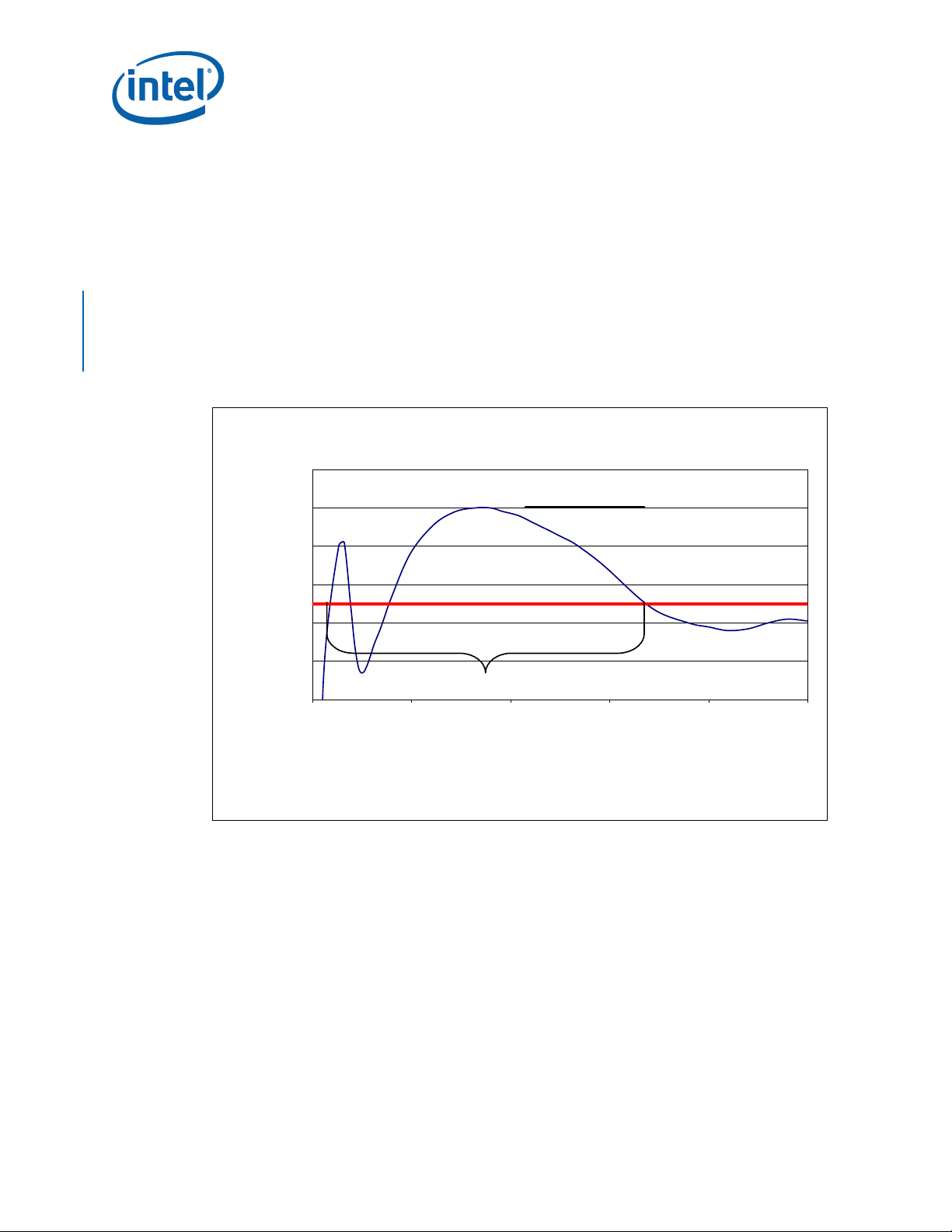
2.4 Processor VCC Overshoot - REQUIRED
The VRM/EVRD 11.0 is permitted short transient overshoot events where Vcc exceeds
the VID voltage when transitioning from a high-to-low current load condition
(Figure 2-2). This overshoot cannot exceed VID + VOS_MAX. The overshoot duration,
which is the time that the overshoot can remain above VID, cannot exceed TOS_MAX.
These specifications apply to the processor die voltage as measured across the remote
sense points and should be taken with the oscilloscope bandwidth setting limited to
20 MHz or 100 MHz, depending what is supported by your particular scope (with
20 MHz preference).
• VOS_MAX = Maximum overshoot voltage above VID = 50 mV
• TOS_MAX = Maximum overshoot time duration above VID = 25 µs
Figure 2-2. Processor Vcc Overshoot Example Waveform
V
VID + 0.050
OS
Voltage [V]
VID - 0.000
T
OS
0 5 10 15 20 25
Time [us]
TOS: Overshoot time above VID
: Overshoot voltage above VID
V
OS
2.5 Impedance vs. Frequency - EXPECTED
Vcc power delivery designs can be susceptible to resonance phenomena capable of
creating droop amplitudes that violate the load line specification. This is due to the
frequency varied PCB, output decoupling and socket impedances from the power plane
layout structures. Furthermore, these resonances may not be detected through
standard time domain validation and require engineering analysis to identify and
resolve.
Impedance vs. Frequency, Z(f) performance simulations of the power delivery network
is a strongly recommended method to identify and resolve these impedances, in
addition to meeting the time domain load line in Section 2.2 and Section 2.3. The
decoupling selection needs to be analyzed to ensure that the impedance of the
decoupling is below the load line target up to the F
in Figure 2-3. Frequency domain load line and overshoot compliance is expected across
the 0 Hz to FBREAK bandwidth. The power delivery frequency response is largely
BREAK (2 MHz) frequency as defined
16 315889-002
Page 17
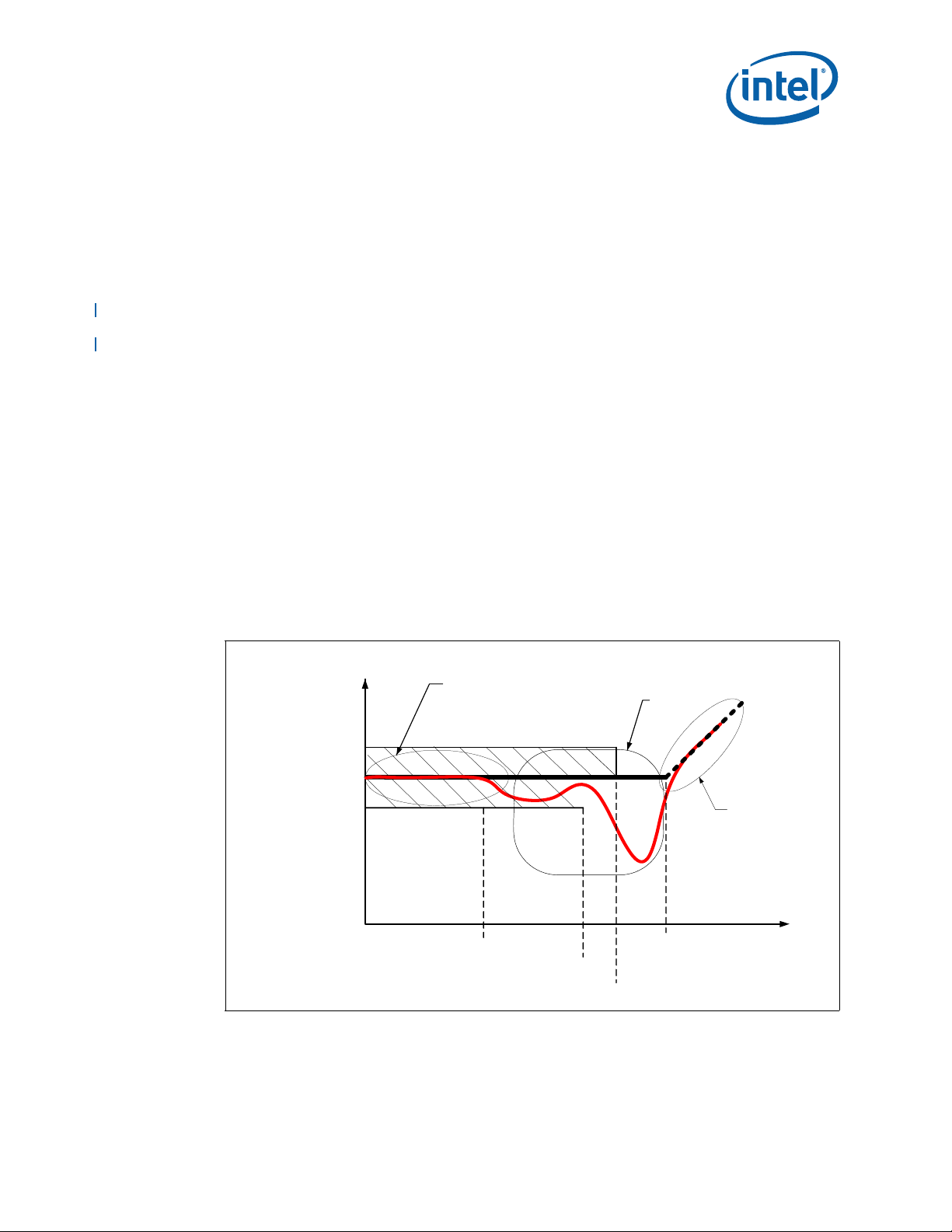
Output Voltage Requirements
dependent upon the selection of the bulk capacitors, ceramic capacitors, power plane
routing and the tuning of the PWM controller’s feedback network. This analysis can be
done with LGA771-V2 VTT tool impedance testing or through power delivery simulation
if the designer can extract the parasitic resistance and inductance of the power planes
on the motherboard along with good models for the decoupling capacitors.
Measured power delivery impedance should be within the tolerance band shown in
Figure 2-3. The tolerance band is defined for the VTT impedance measurement only.
For load line compliance, time domain validation is required and the VR tolerance band
must be met at all times. Above 500 kHz, the minimum impedance tolerance is not
defined and is determined by the MLCC capacitors required to get the ESL low enough
to meet the load line impedance target of the F
tolerance drops to the load line target impedance. Any resonance point that is above
the ZMAX line needs to be carefully evaluated with the time domain method by applying
transient loads at that frequency and looking for V
the impedance profile up to FBREAK is important to ensure the package level decoupling
properly matches the motherboard impedance. After FBREAK, the impedance
measurement is permitted to rise at an inductive slope. The motherboard VR designer
does not need to design for frequencies over F
package decoupling takes over in the region above FBREAK.
Each of these design elements should be fully evaluated to create a cost optimized
solution, capable of satisfying the processor requirements. Experimental procedures for
measuring the Z(f) profile will be included (shortly) in the next revision of the
EVRD_VRM11_0_LL_dVID LGA771_775-V2 VTT Tester-UG.pdf Test Methodology User’s
Guide using the VTT. Additional background information regarding the theory of
operation is provided in Appendix A.
BREAK frequency. At 700 kHz, the ZMAX
MAX or VMIN violations. Maintaining
BREAK as the Intel Microprocessor
Figure 2-3. Power Distribution Impedance vs. Frequency
Zone 1
PWM Droop control
& compensation BW
Z
LL Max
Z target = Z
Z
LL
LL Min
VR BW
500 kHz
Notes:
1. Zone 1 is defined by the VR closed loop compensation bandwidth (VR BW) of the voltage regulator.
Typically 30-40 kHz for a 300 kHz voltage regulator design
2. Zones 2 & 3 are defined by the output filter capacitors and interconnect parasitic resistance and
inductance. The tolerance is relaxed over 500 kHz allowing the VR designer freedom to select output filter
capacitors. The goal is to keep Z(f) below Z
bulk cap values, type and quantity of MLCC capacitors. The ideal impedance would be between Z
Z
LLMin, but this may not be achieved with standard decoupling capacitors.
LL up to FBREAK (2 MHz) and as flat as practical, by selection of
Zone 2
Output Filter
Bulk & MLCC
700 kHz
F
Zone 3
Inductive effects
MLCC ESL +
Socket
Hz
break
LL and
315889-002 17
Page 18

Output Voltage Requirements
3. See Section 2.5 and Ta bl e 2 -4 , Impedance Measurement parameters and definitions
Table 2-4. Impedance Z
Processor
Dual-Core Intel
Dual-Core Intel
Dual-Core Intel
Dual-Core Intel
Dual-Core Intel
Quad-Core Intel
Quad-Core Intel
Quad-Core Intel
Dual-Core Intel
Dual-Core Intel
Dual-Core Intel
Quad-Core Intel
Quad-Core Intel
Quad-Core Intel
Quad-Core Intel
Quad-Core Intel
Quad-Core Intel
Dual-Core Intel
Quad-Core Intel
®
Xeon® Processor 5000 Series 1.25 mΩ 1.45 mΩ 1.05 mΩ 2.0 MHz
®
Xeon® Processor 5000 Series MV 1.25 mΩ 1.511 mΩ 0.989 mΩ 2.0 MHz
®
Xeon® Processor X5100 Series -Perf. 1.25 mΩ 1.583 mΩ 0.917 mΩ 2.0 MHz
®
Xeon® Processor E5100 Series 1.25 mΩ 1.583 mΩ 0.92 mΩ 2.0 MHz
®
Xeon® Processor L5100 Series LV 1.25 mΩ 1.917 mΩ 0.583 mΩ 2.0 MHz
®
Xeon® processor X5300 Series -Perf. 1.25 mΩ 1.49 mΩ 1.01 mΩ 2.0 MHz
®
Xeon® processor E5300 Series 1.25 mΩ 1.583 mΩ 0.917 mΩ 2.0 MHz
®
Xeon® processor L5300 Series- LV 1.25 mΩ 1.750 mΩ 0.750 mΩ 2.0 MHz
®
Xeon® Processor X5200 Series -Perf. 1.25 mΩ 1.583 mΩ 0.917 mΩ 2.0 MHz
®
Xeon® Processor E5200 Series 1.25 mΩ 1.673 mΩ 0.827 mΩ 2.0 MHz
®
Xeon® Processor L5238 Series 1.25 mΩ 1.850 mΩ 0.650 mΩ 2.0 MHz
®
Xeon® processor X5482 Series - Perf. 1.25 mΩ 1.450 mΩ 1.050 mΩ 2.0 MHz
®
Xeon® processor X5400 Series - Perf. 1.25 mΩ 1.490 mΩ 1.010 mΩ 2.0 MHz
®
Xeon® processor E5400 Series 1.25 mΩ 1.544 mΩ 0.956 mΩ 2.0 MHz
®
Xeon® processor L5400 Series 1.25 mΩ 1.750 mΩ 0.750 mΩ 2.0 MHz
®
Xeon® processor X7300 Series - Perf 1.25 mΩ 1.481 mΩ 1.019 mΩ 2.0 MHz
®
Xeon® processor E7300 Series 1.25 mΩ 1.583 mΩ 0.917 mΩ 2.0 MHz
®
Xeon® Processor 7200 Series 1.25 mΩ 1.583 mΩ 0.917 mΩ 2.0 MHz
®
Xeon® processor L7300 Series 1.25 mΩ 1.750 mΩ 0.750 mΩ 2.0 MHz
Measurement Parameter Limits
LL
1
ZLL
ZLLMax
2
ZLLMin
3
Fbreak
Notes
Notes:
1. Z
2. Z
3. Z
is the target impedance for each processor and Z(f) value coincides with it’s Load Line slope.
LL
is the max allowed Z
LLMAX
in Table 2 -3 ; Z
IccMax.
is the min allowed Z
LLMIN
in Table 2 -3 ; Z
IccMax.
is specific for each processor due to a specific combination of its Load Line value and
LLMAX
is specific for each processor due to a specific combination of its Load Line value and
LLMIN
tolerance, which still fits within the VccMax and VccMin Load Line limits listed
LL
tolerance, which still fits within the VccMax and VccMin Load Line limits listed
LL
2.6 Stability - REQUIRED
The VRM/EVRD needs to be unconditionally stable under all specified output voltage
ranges, current transients of any duty cycle, and repetition rates of up to 2 MHz. The
VRM/EVRD should also be stable under a no load condition.
2.7 Processor Power Sequencing - REQUIRED
The VRM/EVRD must support platforms with defined power-up sequences. Figure 2-4
shows a timing diagram of the power-on sequencing requirements. Timing parameters
for the power-on sequence are listed in Table 2 -5 .
18 315889-002
Page 19

Output Voltage Requirements
Figure 2-4. Power-On Sequence Timing Diagram
BCLK [1:0]
(for reference only)
PWM Vcc
(5V/12V)
Tf
Ta
VTT
VTT_PWRGD
OUTEN
VID_SELECT
(pulled up to VTT)
Vcc_CPU
Tg
V
BOOT
Tc
=1.1V
Td
Te
Tb
VR_READY
VID bits
/ BSEL[2:0]
CPU_PWGOOD (from platform, for reference only)
(for reference only)
(for reference only)
Notes:
1. VTT_PWRGD can be designed to be driving directly the OUTEN input.
2. Tb and Td voltage slopes are determined by soft start logic of the PWM controller.
3. Vboot is a default power-on Vcc (Core) value. Upon detection of a valid Vtt supply, the PWM controller is to
4. VTT is the processor termination regulator’s output voltage and the VTT_PWRGD is the VTT regulator’s
5. Unless otherwise noted, all specifications in this table apply to all processor frequencies.
6. This specification requires that the VID signals be sampled no earlier than 10 µs after VCC (at VCC_BOOT
7. Parameter must be measured after applicable voltage level is stable. “Stable” means that the power supply
8. The maximum PWRGOOD rise time specification denotes the slowest allowable rise time for the processor.
RESET#
V
CCPLL
regulate to this value until the VID codes are read. The Vboot voltage is 1.1 V
power good status indicator.
voltage) and VTT are stable.
is in regulation as defined by the minimum and maximum DC/AC specifications for all components being
powered by it.
Measured between (0.3 * VTT) and (0.7 * VTT).
VID code read by PWM at the end of Tc
VID valid
Table 2-5. Startup Sequence Timing Parameters (Sheet 1 of 2)
Timing Min Default Max Remarks
Ta =
PWM Vcc & Vtt to OUTEN delay
time
Tb =
Vboot rise time
Tc =
Vboot to VID valid delay time
315889-002 19
02.0 ms5.0 ms
0.05 ms10.5 ms 10.0 ms
0.05 ms
1
3.0 ms
If the actual timing exceeds 2ms, the
VTT VR must be capable of
supporting full Itt surge current
requirement per Proc’s latest EMTS
Programmable soft start ramp;
Measured from 10-90% of slope
Page 20

Output Voltage Requirements
Table 2-5. Startup Sequence Timing Parameters (Sheet 2 of 2)
Timing Min Default Max Remarks
Td =
VccCPU rise time to final VID
Te =
VccCPU to VR_READY
assertion time
Tf =
Vtt rise time
Tg =
OUTEN to Vcc_CPU rising delay time
Note:
1. Minimum delays must be selected in a manner which will guarantee compliance to voltage tolerance
specifications.
0 0.25 ms 2.5 ms
0.05 ms 3.0 ms
0.05 ms 10.0 ms
05.0 ms
Programmable soft start ramp;
Measured from 10-90% of slope
Measured from 10-90% of slope
2.8 Dynamic Voltage Identification (D-VID) REQUIRED
VRM/EVRD 11.0 supports dynamic VID across the entire VID table. The VRM/EVRD
must be capable of accepting voltage level changes of 12.5 mV steps every 5 µs. The
low voltage state will be maintained for at least 50 µs. The worst case settling time,
including line-to-line skew, for the seven VID lines is 400 ns. The VID inputs should
contain circuitry to prevent false tripping or latching of VID codes during the settling
time.
During a transition, the output voltage must be between the maximum voltage of the
high range (“A” in Figure 2-5) and the minimum voltage of the low range (“B”). The
VRM/EVRD must respond to a transition from VID-low to VID-high by regulating its Vcc
output to the range defined by the new final VID code, within 50 µs of the final step.
The time to move the output voltage from VID-high to VID-low will depend on the PWM
controller design, the amount of system decoupling capacitance, and the processor
load.
Figure 2-5 shows operating states as a representative processor changes levels. The
diagram assumes steady state, maximum current during the transition for ease of
illustration; actual processor behavior allows for any dIcc/dt event during the
transitions, depending on the code it is executing at that time. In the example, the
processor begins in a high-load condition. In transitions 1-2 and 2-3, the processor
prepares to switch to the low-voltage range with a transition to a low load condition,
followed by an increased activity level. Transition 3-4 is a simplification of the multiple
steps from the high-voltage load line to the low-voltage load line. Transition 4-5 is an
example of a response to a load change during normal operation in the lower range.
20 315889-002
Page 21

Output Voltage Requirements
Figure 2-5. Processor Transition States
VID High Load Line
VID Low Load Line
2
5
B
4
Figure 2-6 is an example of dynamic VID. The diagram assumes steady state, constant
current during the dynamic VID transition for ease of illustration; actual processor
behavior allows for any dIcc/dt during the transitions, depending on the code it is
executing at that time. Note that during dynamic VID, the processor will not output VID
codes that would disable the voltage regulator output voltage.
Figure 2-6. Dynamic VID Transition States Illustration
ext.
VR11
VR10
table
table
VID 5
VID 1
VID 0
VID 2
VID 1
VID 3
VID 2
VID 4
VID 3
VID 5
VID 4
VID 6
Note: VR11 table – VID 0 and extended VR10 table – VID 6 is reserved for future processors
worst case VID
36 VID steps @ 5 s each step = 180us
400ns
settling time
A
3
Icc-max
1
Upper equals
Final VID - 1.25 m * Icc
450mV
low VID to high VID
Vcc transition
high VID to low VID
Vcc transition
450mV
The diagram assumes steady state, constant current during the dynamic VID
transitions for ease of illustration; actual processor behavior allows for any dIcc/dt
event during the transitions, depending on the code it is executing at that time
Maximum
Vcc
settling
50µs maximum settling
from registering final VID
50µs maximum settling
from registering final VID
Lower equals
Start VID - 1.25 m * Icc -3 0mV
Upper equals
Final VID - 1.25 m * Icc
Lower equals
Start VID - 1.25 m * Icc -3 0mV
The processor load may not be sufficient to absorb all of the energy from the output
capacitors on the baseboard, when VIDs change to a lower output voltage. The VRM/
EVRD design should ensure that any energy transfer from the capacitors does not
impair the operation of the VRM/EVRD, the AC-DC supply, or any other parts of the
system.
315889-002 21
Page 22

Output Voltage Requirements
2.9 Overshoot at Turn-On or Turn-Off - REQUIRED
The core VRM/EVRD output voltage should remain within the load-line regulation band
for the VID setting, while the VRM/EVRD is turning on or turning off, with no over or
undershoot out of regulation. No negative voltage below –100 mV may be present at
the VRM/EVRD output during turn-on or turn-off.
2.10 Output Filter Capacitance - REQUIRED
The output filter capacitance for the VRM/EVRD11.0 based designs will be located on
the baseboard. The system design must ensure that the output voltage of the VRM/
EVRD conforms to the load line of Figure 2-2 and with the baseboard and processor
loads. Table 2 -7 shows the number of decoupling caps recommended and other related
specifications based on updated processor power requirements supported by VRM/
EVRD 11.0.
Table 2-6. Recommended Decoupling and Other Specifications for Supported
(Highest SKU) Processors - Summary
Processor
Dual-Core Intel Xeon ProcessorBased Server platform 8 layer (3PWR 3-GND and 2 SIG)
Dual-Core Intel Xeon ProcessorBased Server platform with Intel
5000 Chipsets 6 layer (2-PWR, 2GND and 2-SIG), 1 oz Cu
Dual-Core Intel Xeon ProcessorBased Server platform with Intel
5000 Chipsets 8 layer (3-PWR, 3GND and 2-SIG), 1 oz Cu
Dual-Core Intel Xeon 5000 Series
processors with Intel 5400 Chipsets
Platform 8-Layer CRB MB
Dual-Core Intel Xeon 7000 Series
processors with Intel 7300 Chipsets
Platform 14-Layer CRB MB
560µF
Alum-
Polymer
17 54
15 44
13 44
12 10 58 1000
18 65 1000 130 150
100µF
MLCC
10µF
MLCC
(0805)
(1206)
(1206)
22 µF
MLCC
Slew Rate
(di/dt)
A/µs
1200 130 150
1200 130 150
1200 130 150
Itdc (A)
Figure 2-7 through Figure 2-10 are recommended examples of baseboard decoupling
solutions and processor loads. Dual-Core Intel Xeon Processor-Based Server decoupling
applies to all Dual-Core Intel Xeon Processor-Based Server/Dual-Core Intel
Processor-Based Server/Dual-Core Intel Xeon Processor-Based Workstation platforms.
The number of capacitors needed could change based on updated processor power
requirements. The values shown are for a four to five phase 200 kHz to 700 kHz
switching 150 A I
ccMAX/130 A IccTDC voltage regulator design with an output inductor
range of 0.15 µH to 0.5 µH. The type and number of bulk decoupling required is
dependent on the voltage regulator design and it is highly recommended that the OEM
work with the VR supplier for an optimal decoupling solution for their system and in
accordance to the processor’s design requirements.
Max Icc
®
Xeon®
(A)
22 315889-002
Page 23

Output Voltage Requirements
Figure 2-7. Six-layer Dual-Core Intel Xeon Processor-Based Server Platform VccP Power
Delivery Impedance Model Path with 1206 Size Caps
VR
15 X 560 uF
Aluminum-Polymer
0.40m
267 pH
Motherboard
35 X 10 uF
MLCC 1206
350 uF
0.09m
34 pH
58 pH
0.51m
90 uF8400 uF
0.4m
134 pH
9 X 10 uF
MLCC 1206
Socket and Package
20 pH
0.33m
VR
Sense
Point
Figure 2-8. Eight-layer Dual-Core Intel Xeon Processor-Based Server Platform VccP
Power Delivery Impedance Model Path with 1206 Size Caps
VR
13 X 560 uF
Aluminum-Polymer
0.46m
307 pH
Motherboard
35 X 10 uF
MLCC 1206
350 uF
0.09m
34 pH
Socket and Package
20 pH
0.33m
VR
Sense
Point
90 uF7280 uF
0.4m
134 pH
9 X 10 uF
MLCC 1206
0.37m54 pH
Figure 2-9. Eight-layer Dual-Core Intel Xeon Processor-Based Server Platform VccP
Power Delivery Impedance Model Path with 0805 Size Caps
PWL
30A to 130A
1000A/uS
PWL
30A to 130A
1000A/uS
VR
17 X 560 uF
Aluminum-Polymer
0.41m
235 pH
Motherboard
45 X 10 uF
MLCC 0805
450 uF
0.22m
25 pH
54 pH
0.43m
90 uF9520 uF
1.1m
122 pH
9 X 10 uF
MLCC 0805
Socket and Package
20 pH
0.33m
VR
Sense
Point
30A to 130A
1000A/uS
PWL
The platform processor decoupling design incorporates fifteen 560 µF Aluminumpolymer bulk capacitors and forty four 10 µF 1206 package ceramic high-frequency
capacitors per processor for a 6 layer board, thirteen 560 µF Aluminum-polymer bulk
capacitors and forty four 10 µF 1206 package ceramic high-frequency capacitors per
processor for a 8 layer board and seventeen 560 µF Aluminum-polymer bulk capacitors
and fifty four 10 µF 0805 package ceramic high-frequency capacitors per processor for
a 8 layer board (Table 2-8). At least nine of the 10 µF capacitors should be placed in the
cavity of the processor socket. The remaining capacitors can be placed under the
processor socket on the backside of the baseboard. The 560 µF capacitors should be
placed along the sides of the processor socket, as close to the socket as the keep-out
zones allow and on the south east side of the processor socket where the bulk of the
power pins are located.
315889-002 23
Page 24

Output Voltage Requirements
Note: The amount of bulk decoupling needed is dependent on the voltage regulator design.
Some multiphase buck regulators may have a higher switching frequency that would
require a different output decoupling solution to meet the processor load line
requirements than described in this document.
Table 2-7. Dual-Core Intel Xeon Processor-Based Server/Dual-Core Intel Xeon
Processor-Based Server-VS/Dual-Core Intel Xeon Processor-Based
Workstation Platform Processor Decoupling Capacitor Recommendations
6 layers, (2 power, 2 ground, 2 signal), 1 oz Cu
Quantity Value Tolerance
15 560 µF Al-Polymer ±20% NA 7 4
35 10 µF 1206 Ceramic ±20% X5R or X6S 3 1.2
9 10 µF 1206 Ceramic ±20% X6S 3 1.2 1
8 layers, (3 power, 3 ground, 2 signal), 1 oz Cu
Quantity Value Tolerance
13 560 µF Al-Polymer ±20% NA 7 4
35 10 µF 1206 Ceramic ±20% X5R or X6S 3 1.2
9 10 µF 1206 Ceramic ±20% X6S 3 1.2 1
8 layers, (3 power, 3 ground, 2 signal), 1 oz Cu
Quantity Value Tolerance
17 560 µF Al-Polymer ±20% NA 7 4
45 10 µF 0805 Ceramic ±20% X5R or X6S 10 1.1
9 10 µF 0805 Ceramic ±20% X6S 10 1.1 1
Notes:
1. Only the decoupling caps inside the socket cavity need to have the temperature coefficient of “X6S”.
Temperature
Coefficient
Temperature
Coefficient
Temperature
Coefficient
ESR
(mΩ)
ESR
(mΩ)
ESR
(mΩ)
ESL
(nH)
ESL
(nH)
ESL
(nH)
Notes
Notes
Notes
Table 2-9. Dual-Core Intel Xeon 7000 Series with Intel 7300 Chipsets Platform Processor
Decoupling Capacitor Recommendations
Quantity Value / Description
18 560µF/2.5V/20%/ Oscon 6.3 3.2
65 22µF/6.3V/20%/ X5R /1206 MLCC 4 0.52
Notes: Dual-Core Intel Xeon 7000 Series processors with Intel 7300 Chipsets baseboard has 14-layers. Refer
24 315889-002
to the latest Dual-Core Intel Xeon 7000 Series processors with Intel 7300 Chipsets Platform Design
Guide for baseboard stack-up details.
ESR
(mΩ)
ESL
(nH)
Notes
Page 25

Output Voltage Requirements
Figure 2-10. Dual-Core Intel Xeon 5000 Series with Intel 5400 Chipsets Platform VccP
Power Delivery Impedance Model Path - Example
VR
Low Fr Caps
12x 560µF
Oscon
6.72mF
0.58 mO
0.33 nH
Motherboard Socket & Package
HF Caps in
0.33 mO
0.56 mO
0.11 nH
socket cavity
9x 10µF
MLCC 1206
90µF
1000A/us
Mid Fr Caps
10x 100µF
MLCC 1210
1mF
0.4 mO
54 pH
0.51 mO
490µF
0.08 mO
HF Caps
49x 10µF
MLCC 1206
20 pH52 pH
20 pH
Sense
Point
30A to
130A
Table 2-10. Dual-Core Intel Xeon 5000 Series with Intel 5400 Chipsets Platform Processor
Decoupling Capacitor Recommendations
Quantity Value Tolerance
12 560 µF Al-Polymer ±20% Oscon 7 4 1
10 100 µF 1210 MLCC ±10% X6S 4 0.52 1
58 10 µF 1206 MLCC ±10% X5R or X6S 5 1 1, 2
Notes:
1. Dual-Core Intel Xeon 5000 Series processors with Intel 5400 Chipsets platform has 8-layer stackup. Refer
to the latest Dual-Core Intel Xeon 5000 Series processors with Intel 5400 Chipsets Platform Design Guide
for baseboard stack-up details.
2. 9 of these HF caps are inside the processor socket cavity.
Temperature
Coefficient
ESR
(mΩ)
ESL
(nH)
Notes
315889-002 25
Page 26

2.11 Shut-Down Response - REQUIRED
Once the VRM/EVRD is operating after power-up, if either the Output Enable signal is
de-asserted or a specific VID off code is received, the VRM/EVRD must turn off its
output (the output should go to high impedance) within 500 ms and latch off until
power is cycled. If the extended VR 10 VID table is selected, the VRM/EVRD should turn
off its output if VID [6:0] = XX11111. If the VR 11.0 VID table is selected, there are
four VID off states; VID [6:0] = 0000000, 0000001, 1111110, or 1111111.
§
Output Voltage Requirements
26 315889-002
Page 27

Control Signals
3 Control Signals
3.1 Output Enable (OUTEN) - REQUIRED
The VRM/EVRD must accept an input signal to enable its output voltage. When
disabled, the regulator’s output should go to a high impedance state and should not
sink or source current. When OUTEN is pulled low during the shutdown process, the
VRM/EVRD must not exceed the previous voltage level regardless of the VID setting
during the shutdown process. Once operating after power-up, it must respond to a
deasserted OUTEN within 500 ms. The circuitry driving OUTEN is an open-collector/
drain signal. It is EXPECTED that the pull-up resistor will be located on the baseboard
and will not be integrated into the PWM controller chip or VRM.
Table 3-1. OUTEN Specifications
Symbol Parameter Min Max Units
VIH Input Voltage High 0.8 3.465 V
VIL Input Voltage Low 0 0.4 V
3.2 Voltage Identification (VID [6:0]) - REQUIRED
The VRM/EVRD must accept a 7-bit code, VID [6:0], from the processor to set the
reference Vcc operating voltage. Two VID code standards are supported within the
VRM/EVRD 11.0 specification. The first is an extended VR 10 table that is fully
compliant to the VRM/EVRD 10.2 standard, but adds an additional bit for 6.25 mV VID
resolution. (See Table 3-3) The second is a VR 11.0 standard defined in Ta bl e 3-4. The
VID_Select pin, Section 3.4, will identify which table is to be used. Designers should
note that although the VR 11.0 VID code is comprised of eight bits, VID 7 is a provision
for future Itanium-based processors. The VID 7 pin should be connected to V
GND on the VRM module’s printed circuit board. The platforms targeted by this design
guideline will only require VID [6:0].
If an “OFF” VID code is received, such as when no processor is installed, the regulator
must disable its output voltage. If this disable code appears during previously normal
operation, the regulator shall turn off its output within 500 ms. The circuitry driving
each VID [6:0] signal can be an open-collector/drain or a push-pull output type gate.
When driven by an open-collector / drain, these VID signals need to be pulled-up to the
processor’s VTT voltage. Consult the appropriate platform design guide for the
recommended pull-up resistor value. A typical value used is 510 Ohms. When driven by
a push-pull output gate, the pull-up resistors are optional. Consult the appropriate
processor EMTS for driver definition. Pull-ups to 12 V or 5 V are not supported by the
CPU package and therefore are not permitted. It is EXPECTED that the pull-up
resistors will be located on the baseboard and will not be integrated into the PWM
controller chip or VRM.
Table 3-2. VID [6:0] Specifications
SS, VO- or
Symbol Parameter Min Max Units Notes
V
IH
V
IL
Note: 1) Other platform components may use VID inputs and may require tighter limits.
315889-002 27
Input High Voltage 0.8 VTT max V 1
Input Low Voltage 0 0.4 V 1
Page 28

Table 3-3. Extended VR 10 Voltage Identification (VID) Table
5
5
5
5
5
5
5
5
5
5
5
5
5
5
5
5
5
5
5
5
5
5
5
5
5
5
5
5
5
5
5
5
5
5
5
5
5
5
5
5
5
5
5
5
5
5
VI D4 VI D3 VI D2 VI D1 VI D0 VI D5 VI D6 Vol t age VI D4 VI D3 VI D2 VI D1 VI D0 VI D5 VI D6 Vol t a ge
400 mV 200 mV 100 mV 50 mV 25 mV 12.5 mV 6. 25 mV (V) 400 mV 200 mV 100 mV 50 mV 25 mV 12.5 mV 6.25 mV ( V)
01010111.6 11010111.2
01010101.5937511010101.19375
01011011.587
01011001.5812511011001.18125
01011111.57
01011101.5687511011101.16875
01100011.562
01100001.5562511100001.15625
01100111.55 11100111.15
01100101.5437511100101.14375
01101011.537
01101001.5312511101001.13125
01101111.52
01101101.5187511101101.11875
01110011.512
01110001.5062511110001.10625
01110111.5 11110111.1
01110101.4937511110101.09375
01111011.487
01111001.481251111100OFF
01111111.47
01111101.468751111110OFF
10000011.462
10000001.4562500000001.08125
10000111.45 00000111.07
10000101.4437500000101.06875
10001011.437
10001001.4312500001001.05625
10001111.42
10001101.4187500001101.04375
10010011.412
10010001.4062500010001.03125
10010111.4 00010111.02
10010101.3937500010101.01875
10011011.387
10011001.3812500011001.00625
10011111.37
10011101.3687500011100.99375
10100011.362
10100001.3562500100000.98125
10100111.35 00100110.97
10100101.3437500100100.96875
10101011.337
10101001.3312500101000.95625
10101111.32
10101101.3187500101100.94375
10110011.312
10110001.3062500110000.93125
10110111.3 00110110.92
10110101.2937500110100.91875
10111011.287
10111001.2812500111000.90625
10111111.27
10111101.2687500111100.89375
11000011.262
11000001.2562501000000.88125
11000111.25 01000110.87
11000101.2437501000100.86875
11001011.237
11001001.2312501001000.85625
11001111.22
11001101.2187501001100.84375
11010011.212
11010001.2062501010000.83125
11011011.187
11011111.17
11100011.162
11101011.137
11101111.12
11110011.112
1111101OFF
1111111OFF
00000011.087
00001011.062
00001111.05
00010011.037
00011011.012
00011111
00100010.987
00101010.962
00101110.95
00110010.937
00111010.912
00111110.9
01000010.887
01001010.862
01001110.85
01010010.837
Control Signals
Note: An OFF VID code is equivalent to de-asserting the output enable input (Section 3.1).
28 315889-002
Page 29

Control Signals
Table 3-4. VR 11.0 Voltage Identification (VID) Table
Note: Only VID [6.0] are used for VRM/EVRD 11.0 platforms. The eighth VID bit is provisional for future
Itanium-based platforms.
3.3 Differential Remote Sense (VO_SEN+/-) REQUIRED
The PWM controller shall include differential sense inputs to compensate for an output
voltage offset of less than 300 mV in the power distribution path. This common mode
voltage is expected to occur due to transient currents and parasitic inductances and is
not expected to be caused by parasitic resistances.
It’s recommended that the remote sense lines’ current draw will not push the actual
Load Line outside of the Load Line limits shown in Ta bl e 2- 3. As a practical guideline to
minimizing offset errors, it is recommended that the combination of the sense resistor
values and the remote sense current draw will result in the total DC voltage offset <=
2mV.
Note: V
315889-002 29
CC_DIE_SENSE, VSS_DIE_SENSE, VCC_DIE_SENSE2 and VSS_DIE_SENSE2 of the processor pins
are to be used as the VR sense input.
Page 30

Figure 3-1. Remote Sense Routing example.
LGA 771 Socket
1 of 9
10µF
In µP
Cavity
Pin AL8
Pin AL7
Pin AN3
Pin AN4
VCC_ DIE_ SENSE2
High Impedance Path
1k 1 %
VSS_ DI E_ SENSE2
VCC_ DI E_ SENSE
VSS_ DIE_ SENSE
High Impedance Path
1k 1 %
10 1%
10 1%
10 1%
10 1 %
Control Signals
VCC/ VSS Feedback
Inputs
EVRD11. 0 Controller or
VRM 11. 0 Connector
Notes: For each processor, refer to the appropriate platform design guide (PDG) for the recommended VR’s
remote sense routing.
The sense lines should be routed based on the following guidelines:
• Route differentially with a maximum of 5 mils separation.
• Traces should be at least 25 mils thick, but may be reduced when routed through
the processor pin field.
• Traces should have the same length.
• Traces should not exceed 5 inches in length and should not violate pulse-width
modulation (PWM) vendor length requirements.
• Traces should be routed at least 20 mils away from other signals.
• Each sense line should include a 0 – 100 Ω, 5% series resistor that is placed close to
the PWM or VRM connector in order to filter noise from the power planes. Designers
should consult with their power delivery solution vendor to determine the
appropriate resistor value.
• Reference a solid ground plane.
• Avoid switching layers.
On a VRM, the positive sense line will be connected to VO_SEN+ and the negative
sense line will be connected to VO_SEN–.
The processor V
CC_DIE_SENSE, VSS_DIE_SENSE, VCC_DIE_SENSE2 and VSS_DIE_SENSE2 pins
should be connected to test points on the baseboard in order to probe the die voltage.
These test points should be as close to the socket pins as possible.
A high impedance path (100X) should be routed to the center of the processor socket
and terminated to one of the nine 10 µF capacitors. This provision serves as a
precautionary regulation point, in the event the EVRD/VRM is powered on and
processor is installed.
30 315889-002
Page 31

Control Signals
3.4 Load Line Select (LL0, LL1, VID_Select) REQUIRED
The VID_Select, LL1 and LL0 control signal form a 3-bit load line selection and will used
to configure the VRM/EVRD to supply the proper load line for the processors. These
signals are programmed by the CPU package pin bonding. The VID_Select control
signal will select the appropriate VR10 or VR11 VID table and remap the VID [6:0] pins
to the appropriate DAC input. The signals are open-collector/drain or equivalent
signals. Table 3-5 shows the VID_Select, LL1, and LL0 pins specification and Ta bl e 3-6
shows equations in how to obtain V
MAX
and V
code. For VRMs a set of additional signals extent the usability of a modular solution,
refer to Figure 6-1.
It is EXPECTED that the pull-up resistors for LL0 and LL1 will be located on the
baseboard and will not be integrated into the VRM. However, the pull-up resistor for
VID_Select should be located on the VRM and to maintain backward compatibility to
VRM 10.2 compliant platforms a pull-down resistor of 10 kΩ is also required. The pulldown resistor is required for VRMs only and not required for EVRDs. Typically, for EVRD
converters, this signal will be pulled up to VTT (1.1 V/1.2 V) via a 4.7 kΩ resistor. As an
option, 3.3 V with ± 5% regulation tolerance, may be used instead of VTT for VRM or
EVRD converters. Pull-ups to 12 V or 5 V are not supported by the CPU package.
The VR 10 and VR 11.0 VID pins do not have the same voltage weight. See Tabl e 3-6
for the VID bit mapping.
based on LL0, LL1, and VID_Select bit
MIN
Table 3-5. LL0, LL1, VID_Select Specifications
Symbol Parameter Min Max Units
I
OL
V
IH
V
IL
Output Low Current 0 4 mA
Input Voltage High 0.8 3.465 V
Input Voltage Low 0 0.4 V
Table 3-6. VID Bit Mapping
VR 10.x - VID 4 VID 3 VID 2 VID 1 VID 0 VID 5 VID 6
bit
weight
VR 11.0 VID 7 VID 6 VID 5 VID 4 VID 3 VID 2 VID 1 VID 0
800mV 400mV 200mV 100mV 50mV 25mV 12.5mV 6.25mV
§
315889-002 31
Page 32

Control Signals
32 315889-002
Page 33

Input Voltage and Current
4 Input Voltage and Current
4.1 Input Voltages - EXPECTED
The power source for the VRM/EVRD is 12 V +5% / –8%. This voltage is supplied by a
separate power supply. For input voltages outside the normal operating range, the
VRM/EVRD should either operate properly or shut down.
4.2 Load Transient Effects on Input Current EXPECTED
The design of the VRM/EVRD, including the input power delivery filter, must ensure that
the maximum slew rate of the input current does not exceed 0.5 A/µs, or as specified
by the separate power supply.
Note: In the case of a VRM design, the input power delivery filter may be located either on
the VRM or on the baseboard. The decision for the placement of the filter will need to
be coordinated between the baseboard and VRM designers.
It is recommended that the bulk input decoupling (with optional series 0.1-1 µH
inductor) be placed on the baseboard by the VRM input connector and high frequency
decoupling on the VRM module. Expected baseboard decoupling should be between
1000 µF to 2240 µF depending on VRM design and system power supply.
§
315889-002 33
Page 34

Input Voltage and Current
34 315889-002
Page 35

Processor Voltage Output Protection
5 Processor Voltage Output
Protection
These are features built into the VRM/EVRD to prevent fire, smoke or damage to
itself, the processor, or other system components.
5.1 Over-Voltage Protection (OVP) - EXPECTED
The OVP circuit monitors the processor core voltage (Vcc) for an over-voltage
condition. If the output is more than 200 mV above the VID level, the VRM/EVRD shuts
off the output.
5.2 Over-Current Protection (OCP) - EXPECTED
The core VRM/EVRD should be capable of withstanding a continuous, abnormally low
resistance on the output without damage or over-stress to the unit. Output current
under this condition will be limited to no more than 120% of the maximum peak rated
output of the voltage regulator at thermal equilibrium under the specified ambient
temperature and airflow.
§
315889-002 35
Page 36

Processor Voltage Output Protection
36 315889-002
Page 37

Output Indicators
6 Output Indicators
6.1 Voltage Regulator Ready (VR_Ready) - REQUIRED
The VRM/EVRD VR_Ready signal is an output signal that indicates the start-up
sequence is complete and the output voltage has moved to the programmed VID value.
This signal will be used for start-up sequencing for other voltage regulators, clocks, and
microprocessor reset. This signal is not a representation of the accuracy of the DC
output to its VID value.
The platform VR_Ready signal(s) will be connected to logic to assert CPU or system
PWRGD. The value of the resistor and the pull-up voltage will be determined by the
circuitry on the baseboard that is receiving this signal. Typically a 1 kΩ pull to 3.3 V is
used. This signal should not be de-asserted during dynamic VID operation. It should
remain asserted during normal DC-DC operating conditions and only de-assert for fault
shutdown conditions. It will be an open-collector/drain or equivalent signal. The pull-up
resistor and voltage source will be located on the baseboard. Table 6 -1 shows the
VR_Ready pin specification.
Table 6-1. VR_Ready Specifications
Symbol Parameter Min Max Units
I
OL
V
OH
V
OL
Output Low Current 1 4 mA
Output High Voltage 0.8 3.465 V
Output Low Voltage 0 0.4 V
6.2 Voltage Regulator Hot (VR_hot#) - PROPOSED
The VRM/EVRD VR_hot# signal is an output signal that is asserted low when a thermal
event is detected in the converter. Assertion of this signal will be used by the system to
minimize damage to the converter due to the thermal conditions. Tab le 6-2 shows the
VR_hot# signal specification. This signal will be an open-collector/drain or equivalent
signal and needs to be pulled up to an appropriate voltage through a pull-up resistor on
the baseboard. A typical implementation would be a 50 Ω ±5% resistor pulled up to
1.1 V/1.2 V. For platforms using a voltage higher than 1.1 V /1.2 V, a voltage level
translation is required. Processors do not tolerate such voltage levels directly. Consult
the appropriate PDG.
Table 6-2. VR_hot# Specifications
Symbol Parameter Min Max Units
I
OL
V
OH
V
OL
Each customer is responsible for identifying maximum temperature specifications for all
components in the VRM/EVRD design and ensuring that these specifications are not
violated while continuously drawing specified Icc (TDC) levels. In the occurrence of a
thermal event, a thermal sense circuit may assert the processor’s FORCEPR# signal
immediately prior to exceeding maximum VRM, baseboard, and/or component thermal
ratings to prevent heat damage. The assertion may be made through direct connection
Output Low Current 19.9 30 mA
Output High Voltage 0.8 3.465 V
Output Low Voltage 0 0.4 V
315889-002 37
Page 38

to the FORCEPR# pin or through system management logic. Assertion of this signal will
lower processor power consumption and reduce current draw through the voltage
regulator, resulting in lower component temperatures. Sustained assertion of the
FORCEPR# pin will cause noticeable platform performance degradation and should not
occur when drawing less than the specified thermal design current for a properly
designed system.
It is recommended that hysteresis be designed into the thermal sense circuit to prevent
a scenario in which the VR_hot# signal is rapidly being asserted and de-asserted.
6.3 Load Indicator Output (Load_Current) PROPOSED
The VRM/EVRD may have an output with a voltage (Load_Current) level that varies
linearly with the VRM/EVRD output current. The PWM controller supplier may specify a
voltage-current relationship consistent with the controller’s current sensing method.
Baseboard designers may route this output to a test point for system validation.
6.4 VRM Present (VRM_pres#) - EXPECTED
The VRM should have the VRM_pres# signal. This signal is an output signal used to
indicate to the system that a VRM 10.x compatible module is plugged into the socket.
VRM_pres# is an open-collector/drain or equivalent signal. Table 6-3 shows the
VRM_pres# pin specification. It is EXPECTED that the pull-up resistor will be located
on the baseboard and will not be integrated into the VRM.
Output Indicators
Table 6-3. VRM_pres# Specifications
Symbol Parameter Min Max Units
I
OL
V
OH
V
OL
Output Low Current 0 4 mA
Output High Voltage 0.8 5.5 V
Output Low Voltage 0 0.4 V
6.5 VR_Identification (VR_ID#) - EXPECTED
The VRM should have the VR_ID# signal. This signal is an output signal used to
indicate to the system that a VR11-compatible VRM is plugged into the socket.
VR_ID# is an open-collector/drain or equivalent signal. Tab le 6-4 shows the VR_ID#
pin specification. It is EXPECTED that the pull-up resistor will be located on the
baseboard and will not be integrated into the VRM.
The VR_ID# signal combined with the VRM_pres# signal forms a two-bit VRM
identification code to indicate the type of module installed in a system. Figure 6-1
defines the two signal decode.
Table 6-4. VRM_ID# Specifications
Symbol Parameter Min Max Units
I
OL
V
OH
V
OL
Output Low Current 0 4 mA
Output High Voltage 0.8 5.5 V
Output Low Voltage 0 0.4 V
38 315889-002
Page 39

Output Indicators
V
V
)
p
VR
10
2
VR
11
0
Figure 6-1. VRM 11.0 and Platform Present Detection
RM_Pres#
(MB Pull-up,
VRM Pull-
DWN)
00 0 00
.
00 0 01
00 0 10Possible, ref Table 2-3 Possible, ref Table 2-3
mode
00 0 11
00 1 00
.
00 1 01
00 1 10
mode
00 1 11
0 1 0 0 0 N/A No Turn On VRM 10.2 present Not possible, no pullup for VR_ID#
0 1 0 0 1 N/A No Turn On VRM 10.2 present Not possible, no pullup for VR_ID#
0 1 0 1 0 N/A No Turn On VRM 10.2 present Not possible, no pullup for VR_ID#
0 1 0 1 1 N/A No Turn On VRM 10.2 present Not possible, no pullup for VR_ID#
0 1 1 0 0 N/A No Turn On VRM 10.2 present Not possible, no pullup for VR_ID#
0 1 1 0 1 N/A No Turn On VRM 10.2 present Not possible, no pullup for VR_ID#
0 1 1 1 0 N/A No Turn On VRM 10.2 present Not possible, no pullup for VR_ID#
0 1 1 1 1 N/A No Turn On VRM 10.2 present Not possible, no pullup for VR_ID#
1 0 0 0 0 N/A no module present Not possible, no pullup for VR_ID#
1 0 0 0 1 N/A no module present Not possible, no pullup for VR_ID#
1 0 0 1 0 N/A no module present Not possible, no pullup for VR_ID#
1 0 0 1 1 N/A no module present Not possible, no pullup for VR_ID#
1 0 1 0 0 N/A no module present Not possible, no pullup for VR_ID#
1 0 1 0 1 N/A no module present Not possible, no pullup for VR_ID#
1 0 1 1 0 N/A no module present Not possible, no pullup for VR_ID#
1 0 1 1 1 N/A no module present Not possible, no pullup for VR_ID#
1 1 0 0 0 N/A no module present no module present
1 1 0 0 1 N/A no module present no module present
1 1 0 1 0 N/A no module present no module present
1 1 0 1 1 N/A no module present no module present
1 1 1 0 0 N/A no module present no module present
1 1 1 0 1 N/A no module present no module present
non-valid code
1 1 1 1 0 N/A no module
RID#
(MB
PullUP,
VRM Pull
DWN
VID_SELECT
(VRM Pulldwn,
Platform
pullup)
LL1
(MB
PullUP,
CPU Pull
DWN)
Outcome VRD11.0 Module
LL0
(MB
Pull UP,
CPU Pull
(130Atdc, 150Apk, VID11.0
and VID10.2 compat, 30mV
DWN)
Outcome in VRM11.0
tol)
Possible, ref Table 2-3 Possible, ref Table 2-3 Reserved
Possible, ref Table 2-3 Possible, ref Table 2-3 Reserved
Possible, ref Table 2-3 Possible, ref Table 2-3 Reserved
Possible, ref Table 2-3 Possible, ref Table 2-3 Not possible, no pullup for VID_Select
Possible, ref Table 2-3 Possible, ref Table 2-3 Not possible, no pullup for VID_Select
Possible, ref Table 2-3 Possible, ref Table 2-3 Not possible, no pullup for VID_Select
Possible, ref Table 2-3 Possible, ref Table 2-3 Not possible, no pullup for VID_Select
Platform
resent no module present
Outcome in VRM10.2 Platform
(VRM11.0 Backward Compatible;
VR10.2 platform doesn't have
VR_ID# and VID_Select)
Dual-Core Intel® Xeon® 7100 series
processors (1.25mOHM / VID10.2)
§
315889-002 39
Page 40

Output Indicators
40 315889-002
Page 41

VRM – Mechanical Guidelines
7 VRM – Mechanical Guidelines
7.1 VRM Connector - EXPECTED
The part number and vendor name for VRM 11.0 connectors that can be found in
Tabl e 7-1 . The VRM reference in Section 7.2, Section 7.3 and Section 7.4, is based on
the Tyco*/Elcon* interface with the system board is a 27-pin pair edge connector. The
connector uses latches to hold the VRM in place. The connector will be rated to handle
a continuous load current of 130 A.
Table 7-1. VRM 11.0 Connector Part Number and Vendor Name
Connector Vendor Part Number Notes
1651929-1 (Solder Tail)
Tyco / Elcon
Molex
1766336-1 (Surface Mount)
1766436-1 (Press-Fit)
Molex iCool* VRM 24 signal 70 power pins
87787-1012 (Vertical, TH)
87786-1011 (Vertical, SM)
87818-1011 (Right Angle, TH)
1
1, 2
Notes:
1. These vendors are listed by Intel as a convenience to Intel's general customer base, but Intel does not
make any representations or warranties whatsoever regarding quality, reliability, functionality, or
compatibility of these devices. This list and/or these devices may be subject to change without notice.
2. An alternative connector has been identified by Molex for VRMs. This alternative provides many optional
connector variants already in production in both vertical and horizontal (right angle) implementation.
Contact your Molex representative for pin assignment, mechanical form factor details and performance
characteristic data.
7.2 VRM (Tyco/Elcon) Connector Keying
7.2.1 Connector Keying
• Single notch between pins 3 and 4 (51 and 52 opposite side).
• Single notch between pins 12 and 13 (42 and 43 opposite side).
• Single notch between pins 21 and 22 (33 and 34 opposite side).
7.2.2 Connector Pin 1 Orientation
Referencing Figure 7-1, Outline Drawing, Far Side (FS) pins sequence 1 through 27, left
to right. Near Side (NS) pins sequence 54 through 28. Pin 1 and 54 are opposite one
another.
7.3 Pin Descriptions and Assignments
Tabl e 7-2 shows the VRM11.0 connector pin description. Pin assignments are shown in
Tabl e 7-1 .
315889-002 41
Page 42

Table 7-2. VRM 11.0 Connector Pin Descriptions
Name Type Description
Load_Current Output Analog signal representing the output load current
OUTEN Input Output enable
VR_Ready Output Output signal indicating that the start-up sequence is complete and the
VID [6:0]
VIN+ Power VRM Input Voltage
VIN− Ground VRM Input Ground
VO+ Power VRM Output Voltage
VO− Ground VRM Output Ground
VO_SEN+
VO_SEN–
VR_hot# Output Indicates to the system that a thermal event has been detected in the VR
VRM_pres# Output Indicates to the system that a VR10-compatible VRM is plugged into the
VR_ID# Output Indicates to the system that a VR11-compatible VRM is plugged into the
LL0, LL1 Input Used to configure VR load line value
VID_Select Input Used to select between extended VR10 and VR11 VID tables
1
Input Voltage ID pins used to specify the VRM output voltage
Input Output voltage sense pins
output voltage has moved to the programmed VID value.
socket
socket
VRM – Mechanical Guidelines
Note: VID7 bit is not routed from the PWM control IC to the VRM connector; VID7is to be held Low on the VRM
board.
42 315889-002
Page 43

VRM – Mechanical Guidelines
Figure 7-1. VRM 11.0 Pin Assignments
1 VIN− 54 VIN+
2 VIN− 53 VIN+
KEY
KEY
KEY
3 VIN− 52 VIN+
4 VID4 51 VID3
5 VID2 50 VID1
6 VID0 49 VID5
7 VO_SEN+ 48 VO_SEN−
8 VR_Ready 47 VR_hot#
9 OUTEN 46 LL0
10 Load_Current 45 LL1
11 VID6 44 VID_Select
12 VRM_pres# 43 VR_ID#
13 VO+ 42 VO+
14 VO+ 41 VO+
15 VO+ 40 VO+
16 VO− 39 VO−
17 VO− 38 VO−
18 VO− 37 VO−
19 VO+ 36 VO+
20 VO+ 35 VO+
21 VO+ 34 VO+
22 VO− 33 VO−
23 VO− 32 VO−
24 VO− 31 VO−
25 VO+ 30 VO+
26 VO+ 29 VO+
27 VO+ 28 VO+
KEY
KEY
KEY
7.4 Mechanical Dimensions - PROPOSED
The mechanical dimensions for the VRM 11.0 module and connector are shown in
Figure 7-1.
7.4.1 Gold Finger Specification
The VRM board must contain gold lands (fingers) for interfacing with the VRM
connector that is 1.50 mm ±0.2 mm [0.059” ±0.008”] wide by 6.00 mm [0.236”]
minimum long and spaced 2.50 mm [0.098”] apart. Traces from the lands to the power
plane should be a minimum of 0.89 mm [0.035”] wide and of a minimal length.
315889-002 43
Page 44

Figure 7-1. VRM 11.0 Module and Connector
96.52mm (3.80") MAX
VRM – Mechanical Guidelines
15.50mm
(0.610")
9.03mm
(0.356")
MAX
51.84mm
(2.04”)
13.50mm
(0.531")
3.00mm
(0.118")
13.18mm
(0.519")
PIN 54
PIN 1
PIN 54
3.33mm
(0.131")
PIN 1
2X R2.00mm (R0.08")
Component
Keepout
1.70mm
(0.067")
22.97mm
(0.904")
OPEN Latches 114.98mm (4.527") MAX
CLOSED Latches 102.5mm (4.035") MAX
36.07mm (1.420")
10.53mm(0.415")
5.08mm
(0.200")
PCB Footprint
View A
93.34mm (3.675") MAX
NEAR SIDE Components
FAR SIDE Components
Connector Length 97.54mm (3.840") MAX
66.77mm (2.629")
8x2.50mm
(0.098")
7.87mm (0.310")
28.9mm
(1.138")
9.70mm (0.382")
hole diameter
54x1.02+/-0.08mm
(.040+/-.003")
22.88mm
(0.901")
12x2.50mm
(0.098")
View B
PIN 28
8.04mm
(0.316")
65.34mm
(2.57")
MAX
10.16mm
(0.4")
MAX
(0.059 +/- 0.008")
14.27mm
(0.562")
MAX
R 0.65mm
(R0.026")
20.0mm
(0.79")
1.50+/- 0.2mm
1.80mm
(0.071")
View B
4.05mm
(0.159")
59.3mm
(2.33")
Ref.
7.0mm
(0.276")
View A
1.00+0/- 0.13mm
(0.039+0/-0.005")
PCB
Edge Card
Cont acts
1.57mm +/- 0.20
66.34mm
(2.612")
MAX
12.0mm
(0.47")
6.00mm
(0.236")
30
0.50mm
(.020")
(.062" +/-.008)
§
44 315889-002
Page 45

Environmental Conditions
8 Environmental Conditions
The VRM/EVRD design, including materials, should meet the environmental
requirements specified below.
8.1 Operating Temperature - PROPOSED
The VRM/EVRD shall meet all electrical requirements when operated at the Thermal
Design Current (Icc
minimum airflow of 400 LFM (2 m/s). The volumetric airflow (Q) can be measured
through a wind tunnel. For testing, the baseboard should be mounted in a duct. (A VRM
should be mounted on a PCB, and then mounted in a duct.) The recommended duct
cross-section, assuming the PCB is horizontal and flush with the bottom of the duct, is
as follows:
• Y direction duct width (perpendicular to flow, horizontal) = 0.3 m
• Z direction duct height (perpendicular to flow, vertical) = 0.15 m
• Minimum X direction duct length in front of VRM = 6 hydraulic diameters = 1.2 m
• Minimum X direction duct length behind VRM = 2 hydraulic diameters = 0.4 m
• Velocity (v) is calculated from the volumetric flow and cross-sectional area at the
inlet as:
• v = Q/(0.3 x 0.15)m2 Operating conditions shall be considered to include 10 cycles
between min and max temperature at a rate of 10ºC/hour and a dwell time of 30
minutes at extremes. Temperature and airflow measurements should be made in
close proximity to the VRM.
) over an ambient temperature range of 0ºC to +45ºC with a
TDC
8.2 VRM Board Temperature - REQUIRED
To maintain the connector within its operating temperature range, the VRM board
temperature, at the connector interface, shall not exceed a temperature equal to 90ºC.
At no time during the operation is the board permitted to exceed 90ºC within a distance
of 2.54 mm [0.100”] from the top of connector (0.4 in. from board edge). In order not
to exceed 90ºC, it is recommended that the board be constructed from 2-ounce copper
cladding. Temperature and airflow measurements should be made in close proximity to
the VRM.
8.3 Non-Operating Temperature - PROPOSED
The VRM/EVRD shall not be damaged when exposed to temperatures between –40ºC
and +70ºC. These shall be considered to include 50 cycles of minimum to maximum
temperatures at 20ºC/hour with a dwell time of 20 minutes at the extremes.
8.4 Humidity - PROPOSED
85% relative – operating
95% relative – non-operating
315889-002 45
Page 46

8.5 Altitude - PROPOSED
3.05 km [10 k feet] – operating
15.24 km [50 k feet] – non-operating
8.6 Electrostatic Discharge - PROPOSED
Testing shall be in accordance with IEC 61000-4-2.
Operating – 15 kV initialization level. The direct ESD event shall cause no out-ofregulation conditions – including overshoot, undershoot and nuisance trips of overvoltage protection, over-current protection or remote shutdown circuitry.
Non-operating –25 kV initialization level. The direct ESD event shall not cause damage
to the VRM circuitry.
8.7 Shock and Vibration - PROPOSED
The shock and vibration tests should be applied at the baseboard level. The VRM/EVRD
should not be damaged and the interconnect integrity not compromised during:
• A shock of 50 g (± 10%) with velocity change of 170 inches/sec (± 10%) applied
three times in each of the orthogonal axes.
• Vibration of 0.01 g² per Hz at 5 Hz, sloping to 0.02 g² per Hz at 20 Hz and
maintaining 0.02 g² per Hz from 20 Hz to 500 Hz for 10 minute per axis applied in
each of the orthogonal axes.
Environmental Conditions
8.8 Electromagnetic Compatibility - PROPOSED
Design, including materials, should be consistent with the manufacture of units that
comply with the limits of FCC Class B and CISPR22 Class B for radiated emissions.
8.9 Reliability - PROPOSED
Design, including materials, should be consistent with the manufacture of units with a
Mean Time Between Failure (MTBF) of 500,000 hours of continuous operation at 55ºC,
maximum-outputs load, and worst-case line, while meeting specified requirements.
MTBF should be calculated in accordance with MIL-STD-217F or Bellcore.
8.10 Safety - PROPOSED
The voltage regulator is to be UL Recognized to standard UL1950 3rd Ed., including
requirements of IEC950 and EN 60950. Plastic parts and printed wiring board are to be
UL Recognized with 94V-0-flame class.
§
46 315889-002
Page 47

Manufacturing Considerations
9 Manufacturing Considerations
9.1 Lead Free (Pb Free)
The use of lead in electronic products is an increasingly visible environmental and
political concern. The drivers for the reduction or elimination of lead in electronic
products include:
• Customer desire for environmentally friendly (‘green’) products.
• Manufacturer desire to be environmentally friendly, and be perceived as such.
• Government initiatives regarding recycling of electronic products.
• Planned and potential legislation.
The most notable legislation is the European Union (EU) Restriction on Hazardous
Materials directive, also known as RoHS. The commission directive may be found at the
following URL:
http://europa.eu.int/eur-lex/pri/en/oj/dat/2003/l_037/
l_03720030213en00190023.pdf
European Union “Member States shall ensure that, from 1 July 2006, new electrical and
electronic equipment put on the market does not contain lead...” Each EU country will
implement this law and establish penalties and fines for non-compliance. The RoHS
directive includes certain exemptions:
• Lead in high melting temperature type solders (i.e. tin-lead solder alloys containing
more than 85% lead).
• Lead in solders for servers, storage and storage array systems (exemption granted
until 2010).
• Lead in solders for network infrastructure equipment for switching, signaling,
transmission as well as network management for telecommunication.
• Lead in electronic ceramic parts (e.g. piezoelectronic devices).
For the latest information on RoHS please refer to the following URL:
http://europa.eu.int/eur-lex/en
Intel recommends that you consider Pb Free manufacturing processes and components
for the module and module connector.
§
315889-002 47
Page 48

Manufacturing Considerations
48 315889-002
Page 49

Z(f) Constant Output Impedance Design
A Z(f) Constant Output
Impedance Design
A.1 Introduction - PROPOSED
The VRM/EVRD performance specification is based on the concept of output impedance,
commonly known as the load line. The impedance is determined by the Pulse Width
Modulator (PWM) controller’s Adaptive Voltage Positioning (AVP), up to the loop
bandwidth of the regulator and the impedance of the output filter and socket beyond
the loop bandwidth.
®
Figure A-1. Typical Intel
Microprocessor Voltage Regulator Validation Setup
ZPCB1 ZPCB2 ZPskt
Vin
PWM
ZBulk
ZHF1 ZHF2
VFB
VTT
315889-002 49
Page 50

Figure A-2. Z(f) Network Plot with 1.25 mΩ Load Line
Z(f) Constant Output Impedance Design
The impedance plot Z(f) shown in Figure A-2 can be divided up into three major areas
of interest.
• Low frequency, Zero Hz (DC) to the VR loop bandwidth. This is set by AVP and loop
compensation of the VR controller or PWM control IC.
• Middle frequency, VR loop bandwidth to socket inductance rise - This is set by the
bulk capacitors, MLCC capacitors and PCB layout parasitic elements.
• High frequency, controlled by socket inductance and the CPU package design.
The VRM/EVRD designer has control of the low and mid frequency impedance design.
By ensuring these areas meet the load line target impedance in Section 2.2, the system
design will work properly with future CPU package designs.
Figure A-2 shows the impedance vs. frequency network the system in Figure 2-1. This
example consists of 17 560 μF with an ESR of 7 mΩ and ESL of 4 nH per bulk
capacitors, 1
0805 MLCC, with ESR is 10 mΩ and ESL of 1.1 nH, 2
st
PCB impedance of 1.0 μΩ and 0.05 pH between the bulk and 45 10 μF
nd
PCB impedance of 1.0 μΩ and
0.05 pH between the 45 10 μF and the 9 10 μF 0805 MLCC in the socket cavity with ESR
is 10 mΩ and ESL of 1.1 nH, and the LGA771 socket impedance of 330
μΩ and 20 pH.
The resonant point seen at 400 kHz is due to the mis-match between the bulk
capacitors and the MLCC cavity capacitors. Increasing the capacitance values will drop
the magnitude and shift the to a lower resonance frequency. For example, if the 10
capacitors are increased to 22
μF, the resonant peak drops in magnitude to 1.0 mΩ and
μF
at a frequency of 200 kHz. The resonant peak could also be reduced by reducing the
ESL of the bulk capacitors by changing capacitor technology or by adding more bulk
50 315889-002
Page 51

Z(f) Constant Output Impedance Design
capacitors in parallel. The effect of the mid frequency resonant point must be
investigated and validated with Vdroop testing to ensure any current load transient
pattern, does not violate the V
load line.
min
By defining the output impedance load line over a frequency range, the voltage
regulation or voltage droop is defined at any current level as the output current
multiplied by the impedance value. Currently, output impedance is validated in the time
domain by measuring the voltage response to a known current step. In Figure A-1, the
VTT tool replaces the CPU and the package for platform validation purposes. Typical
measured voltage and currents are depicted in Figure A-3. The transient load line is
defined as the voltage droop magnitude during the current rise time divided by the
current step. The static load line is defined as the voltage level magnitude, after
settling, divided by the current step. It is desired to have both the transient and static
load line equal.
Figure A-3. Time Domain Response of a Microprocessor Voltage Regulator
The static and transient load line measurements, measure the quality of different parts
of the voltage regulator design. The transient load line is governed by the parasitic
impedances in the output filter board layout, decoupling capacitors, and power
distribution network. The static load line is governed by the PWM controller's AVP
accuracy. The time domain Vdroop testing method gives pass, fail data on meeting the
target specification, but gives little insight as to how to improve the voltage regulator's
response. It can be difficult to determine if you need more bulk capacitance, more high
frequency MLCC capacitance or higher loop bandwidth from the time domain Vdroop
waveforms. By measuring the impedance, Z(f) of the voltage regulator, these tradeoffs and optimizations can be made.
The impedance can be measured with a network analyzer, but the network analyzer can
only measure the passive filter components and will not show the effects of the VR loop
bandwidth and AVP. Also MLCC capacitors impedance varies with DC bias and AC ripple
315889-002 51
Page 52

Z(f) Constant Output Impedance Design
frequency applied by the application. Hence a better method is needed to extract the
impedance profile with the VR operating. The following sections introduce the theory
behind using a VTT tool to create an impedance profile for the VR system.
A.2 Voltage Transient Tool (VTT) Z(f) Theory
The following expression is the definition of impedance as a function of frequency
looking back from the VTT tool into the filter network and VRM.
tVFFT
fZ =
)(
The representation of the corresponding Fourier spectra of the voltage and current
responses are shown in Figure A-2. The first harmonic values from the Fast Fourier
Transform (FFT) are used in the calculation of Z(f). The ratio of the two, yields the
impedance at a given frequency, f. By sweeping the VTT generated load transient
repetition rate, I(t), over the desired region of interest, additional points are estimated
on the impedance profile to obtain a near continuous impedance spectrum plot.
In the VTT tool, the die voltage, V(t), is brought out through a pair of non-current
carrying remote sense pins, tied to the Vcc and Vss power plane and measured on the
VTT tool substrate. The current, I(t), is a differential voltage measured across the
current shunt resistors in the VTT tool. The oscilloscope's math function is used to
convert the time domain voltage droop and current measurements into their
corresponding frequency domain spectrum. Since the FFT of the actual response
waveforms are calculated, perfect square waves of current are not needed as a
stimulus. The accuracy and frequency response of this method is limited to the current
shunt resistor's accuracy and the shunt's parasitic inductance. Parasitic inductance in
the current shunt resistors will over estimate the actual current and hence the method
will under estimate the impedance at frequencies where the inductive voltage drop
dominates the resistive voltage drop. The 50 pH of parasitic inductance in the VTT
causes an over estimation of current for frequencies over 1 MHz and an under
estimation of impedance. This can be corrected by post processing of the data and
removing the inductive voltage spike.
))((
tIFFT
))((
52 315889-002
Page 53

Z(f) Constant Output Impedance Design
Figure A-4. Time Domain Responses and Corresponding Fourier Spectra
of Voltage, Current and Impedance
A.3 VTT Z(f) Measurement Method
An electronic load that has the capability to change the repetition rate up to 3 MHz of
the load step is needed. The Intel LGA771/775V2 VTT by Cascade Systems Design, will
meet this requirement. By monitoring the VTT current and voltage waveforms with an
oscilloscope capable of executing an FFT on these waveforms, the platform impedance
is found. A complete impedance profile is then generated by sweeping the input
waveform frequency across the range of interest. In order to automate the data
collection process, Intel has modified the VTT control software and a GPIB controlled
oscilloscope is used along with software supplied with the VTT.
These utilities allow the user to automatically display and collect the magnitude and
phase of the motherboard impedance in a Microsoft Excel* compatible data file. The
total time it takes to extract the impedance profile using this method is about 1-2
minutes. This technique is very useful in investigating and assuring MB performance
based on its stack up.
For more information on the measurement method and theory, see the paper
Microprocessor Platform Impedance Characterization using VTT Tools by K. Aygun, S.
Chickamenahalli, K. Eilert, M. Hill, K. Radhakrishnan and E. Stanford published at the
IEEE Applied Power Electronics Conference, 2005.
A.4 Results
As an example, Figure A-5 shows the test platform with 10 560 μF Al-Poly bulk
capacitors and 10 10
cavity. Figure A-6 is the measured impedance profile of the board shown in Figure A-5
as capacitors are removed. The VID setting for this measurement was 1.35 V and load
μF and 8 22 μF high frequency MLCC capacitors in the socket
315889-002 53
Page 54

Z(f) Constant Output Impedance Design
current was 40 A. The waveforms show the effect of capacitor depopulation on the
impedance profile above 1 MHz as pairs of high frequency MLCC capacitors are
removed (banks 1-9) per the bank designations depicted in Figure A-7.
Simulation comparisons are made in Figure A-8 for the two extreme cases of the
decoupling conditions of Figure A-7, with all MLCC plus two Al-Poly bulk capacitors in
place and all cavity MLCCs plus two Al-Poly bulk capacitors removed. Simulation depicts
a 6-layer distributed motherboard model. The VR model has a Type III feedback
compensated switching VR (swvr) and an average model (avgvr). It can be observed
from Figure A-8 that the switching model measurements agrees better beyond the VR
bandwidth (40 kHz) than the average model, while the average VR model performance
agrees with the overall trend. Slightly lower average model impedances are also
observed and other disagreements are attributed to imperfect assumptions about the
parasitics of the devices and specific adaptive voltage implementation in the VR
models.
Figure A-5. Photo of Motherboard Analyzed Showing High Frequency
MLCC Capacitors In the Socket Cavity and Bulk Capacitors
54 315889-002
Page 55

Z(f) Constant Output Impedance Design
Figure A-6. Measured Platform Impedance Profile Showing Change
in Impedance as Capacitors Are Removed
Magnitude of impedance profile
10
9
8
7
6
5
4
magnitude (mohms)
3
2
1
0
all caps installed
1. 2x 10uF removed
2. 2x 10uF removed
3. 2x 10uF removed
4. 2x 22uF removed
5. 10, 22 uF removed
6. 2x 22uF removed
7. 10, 22uF removed
8. 2x 10uF removed
9. 2x 22uF removed
MLCC + 1 Bulk remo ved
MLCC +2 Bulk removed
0.001 0.01 0.1 1 10 100
frequency (MHz)
Figure A-7. Designations of MLCC Cavity Capacitor Banks
9
9
9
9
9
9
5
5
5
5
5
5
7
7
7
7
7
7
4
4
4
4
4
4
1
1
1
1
1
1
3
3
3
3
3
3
6
6
6
6
6
6
2
2
2
2
2
2
8
8
8
8
8
8
10uF
22uF
315889-002 55
Page 56

Z(f) Constant Output Impedance Design
Figure A-8. Simulated and Measured Waveforms of Platform Impedance Profile
measured vs simulated results
10
meas:allcaps
9
meas:bank1-9+2oscons
sim:swvr-allcaps
8
sim:avgvr-allcaps
sim:swvr-bank1-9+2osc
7
sim:avgvr-bank1-9+2osc
6
5
4
impedance (mohms)
3
2
1
0
10
-3
10
-2
10
-1
10
0
10
1
frequency(MHz)
A.5 Output Decoupling Design Procedure
1. Select type and number of bulk capacitors. Normally the equivalent ESR needs to
be approximately ½ the load line target impedance. For a 1.25 mΩ load line, the
equivalent ESR should be less than 0.625 mΩ. The reason for selecting the number
of bulk capacitors to yield an equivalent ESR to be ½ the target impedance is to
compensate for the parasitic resistance of the PCB layout plane shapes and for
aging of the capacitors. This is a starting point for the design. The final number of
bulk capacitors will be determined by transient droop testing and Z(f)
measurements.
2. The type and number of MLCC capacitors in the socket cavity is specified in the
Section 2.10. These are required to meet both power delivery impedance and
signal integrity issues.
3. Design the PWM loop bandwidth compensation. The ideal loop BW is set at the
frequency where the bulk capacitor impedance meets the target impedance curve.
In Figure A-2, it is approximately 30 kHz. Small increases in the loop bandwidth will
not improve system performance until the bandwidth is moved to where the MLCC
impedance meets the target impedance at ~ 700 kHz which is impractical.
Consult the PWM chip manufacturer's data sheets and application notes on calculating
the PWM loop compensation and AVP programming values.
§
56 315889-002
 Loading...