

Page 1

Intel® 31244 PCI-X to Serial ATA
Controller
Design Guide
April 2004
Order Number: 273651-003
Page 2

Intel® 31244 PCI-X to Serial ATA Controller
INFORMATION IN THIS DOCUMENT IS PROVIDED IN CONNECTION WITH INTELR PRODUCTS. EXCEPT AS PROVIDED IN INTEL’S TERMS
AND CONDITIONS OF SALE FOR SUCH PRODUCTS, INTEL ASSUMES NO LIABILITY WHATSOEVER, AND INTEL DISCLAIMS ANY EXPRESS
OR IMPLIED WARRANTY RELATING TO SALE AND/OR USE OF INTEL PRODUCTS, INCLUDING LIABILITY OR WARRANTIES RELATING TO
FITNESS FOR A PARTICULAR PURPOSE, MERCHANTABILITY, OR INFRINGEMENT OF ANY PATENT, COPYRIGHT, OR OTHER
INTELLECTUAL PROPERTY RIGHT.
Intel Corporation may have patents or pending patent applications, trademarks, copyrights, or other intellectual property rights that relate to the
presented subject matter. The furnishing of documents and other materials and information does not provide any license, express or implied, by
estoppel or otherwise, to any such patents, trademarks, copyrights, or other intellectual property rights.
Intel products are not intended for use in medical, life saving, life sustaining, critical control or safety systems, or in nuclear facility applications.
Intel may make changes to specifications and product descriptions at any time, without notice.
Designers must not rely on the absence or characteristics of any features or instructions marked “reserved” or “undefined.” Intel reserves these for
future definition and shall have no responsibility whatsoever for conflicts or incompatibilities arising from future changes to them.
®
The Intel
published specifications. Current characterized errata are available on request.
This Design Guide as well as the software described in it is furnished under license and may only be used or copied in accordance with the terms of
the license. The information in this manual is furnished for informational use only, is subject to change without notice, and should not be construed as
a commitment by Intel Corporation. Intel Corporation assumes no responsibility or liability for any errors or inaccuracies that may appear in this
document or any software that may be provided in association with this document.
Except as permitted by such license, no part of this document may be reproduced, stored in a retrieval system, or transmitted in any form or by any
means without the express written consent of Intel Corporation.
Contact your local Intel sales office or your distributor to obtain the latest specifications and before placing your product order.
Copies of documents which have an ordering number and are referenced in this document, or other Intel literature may be obtained by calling
1-800-548-4725 or by visiting Intel's website at http://www.intel.com.
AnyPoint, AppChoice, BoardWatch, BunnyPeople, CablePort, Celeron, Chips, CT Media, Dialogic, DM3, EtherExpress, ETOX, FlashFile, i386, i486,
i960, iCOMP, InstantIP, Intel, Intel Centrino, Intel logo, Intel386, Intel486, Intel740, IntelDX2, IntelDX4, IntelSX2, Intel Create & Share, Intel GigaBlade,
Intel InBusiness, Intel Inside, Intel Inside logo, Intel NetBurst, Intel NetMerge, Intel NetStructure, Intel Play, Intel Play logo, Intel SingleDriver, Intel
SpeedStep, Intel StrataFlash, Intel TeamStation, Intel Xeon, Intel XScale, IPLink, Itanium, MCS, MMX, MMX logo, Optimizer logo, OverDrive,
Paragon, PC Dads, PC Parents, PDCharm, Pentium, Pentium II Xeon, Pentium III Xeon, Performance at Your Command, RemoteExpress, SmartDie,
Solutions960, Sound Mark, StorageExpress, The Computer Inside., The Journey Inside, TokenExpress, VoiceBrick, VTune, and Xircom are
trademarks or registered trademarks of Intel Corporation or its subsidiaries in the United States and other countries.
*Other names and brands may be claimed as the property of others.
Copyright © 2004, Intel Corporation
31244 PCI-X to Serial ATA Controller may contain design defects or errors known as errata which may cause the product to deviate from
2 Design Guide
Page 3

Intel® 31244 PCI-X to Serial ATA Controller
Contents
Contents
1 About This Document .................................... .. ..... .. ..... ....... ..... .. ..... .. ..... ....... ..... .. ..... .. ..... ..... ...........9
1.1 Reference Documentatio n........ ............... .............. ............................ ............................. ......9
1.2 Terminolog y and Def in i tions ...................... ............................ ............... ............................ ....9
2 Overview........................................................................................................................................13
2.1 Features..............................................................................................................................13
2.2 Applications ........................................................................................................................ 15
3Intel
4 Routing Guidelines........................................................................................................................ 25
5Intel
®
31244 PCI-X to Serial ATA Controller Package ..................................................................17
3.1 Signal Pin Descriptions................................................................................................ .......18
3.1.1 VA0, VA1 (V
3.2 Package/Marking Info rmation.............................................................................................22
3.3 Ball Map By Function..........................................................................................................23
4.1 General Rout ing Guidelines.... ............................. ............................ .............. .....................25
4.2 Crosstalk.............................................................................................................................26
4.3 EMI Considerations ....... .............. ............................ ............................. ............................ ..27
4.4 Power Distrib ut ion and Decouplin g....... ............................. ............................ .....................28
4.4.1 Decoupling.............................................................................................................28
4.4.1.1 Intel
4.5 Trace Impedance ................................................................................................................29
4.5.1 Differential Impedance........................................................................ ................. ..29
®
31244 PCI-X to Serial ATA Controller Interface Ports.........................................................31
5.1 Serial ROM Interface .......................................................................................................... 31
5.2 JTAG Interface....................................................................................................................31
5.3 PCI-X Interf a c e....... .............. ............................ ............................. ............................ .........32
5.4 Serial ATA Interface............................................................................................................33
5.4.1 Direct Port Access (DPA).......................................................................................33
5.4.2 Extended Voltage Mode ..................................................................... ...................33
5.4.3 LED Inte r face...... ............................ ............... ............................ ............................34
5.4.4 Reference Clock Generation ................................................ ....... ................. .........35
) Pin Requirements.............................. ............................ .........21
CCPLL
®
31244 PCI-X to Serial ATA Controller Decoupling.......................28
6 Printed Circuit Board (PCB) Methodology.....................................................................................37
6.1 Intel
6.2 Extended Voltage Mode ................................................................................................... ..39
7 PCI-X Layout Guide lines .................................................... ............................. ..............................47
7.1 PCI Voltage Levels .............................................................................................................47
7.2 PCI/X Clocki ng Modes............ .............. ............................. ............................ .....................48
Design Guide 3
®
31244 PCI-X to Serial ATA Controller
Normal Mode (standard SATA driver) ................................................................................ 38
6.1.1 Intel
6.2.1 Backplane Topologies ........................................................................................... 40
6.2.2 Motherboard Stackup for Backplane Designs.......................................... ............ ..42
6.2.3 Backplane Stripline Stackup.................................................................................. 44
6.2.4 Cable Intercon nect With Backpl ane.......................................................................45
®
31244 PCI-X to Serial ATA Controller HBA Stackup...................................39
Page 4

Intel® 31244 PCI-X to Serial ATA Controller
Contents
7.3 PCI General Layout Guidelines.............................................. ............ ....... ....... ............ ......49
7.4 PCI-X Layout Guidelines For Slot Configurations............................................................... 50
7.4.1 Protection Circuitry for Add-in Cards..................................................................... 50
7.4.2 PCI Clock La yo ut Guide lines............................................... ............................ ......51
7.4.3 Connecting Intel
to Single-Slot ......................................................................................................... 52
7.4.4 Embedded Intel
Single PCI-X Load.................................................................................................53
7.4.5 Embedded Intel
®
31244 PCI-X to Serial ATA Controller
®
31244 PCI-X to Serial ATA Controller
®
31244 PCI-X to Serial ATA Controller
Design With Multiple PCI-X Loa ds.........................................................................54
8 Cables and Connectors.................................................................................................................55
8.1 Cabling................................................................................................................................55
8.1.1 Serial ATA Cable....................................... ............................ ............................ ....58
9 Voltage Power Delivery.......................... ............................. .......................................... ................59
®
9.1 Intel
31244 PCI-X to Serial ATA Controller Core
Supply Voltage: Providing 2.5V in 3.3 V System............................................................... 59
10 Test Methodology.... ......................................................................................................................61
10.1 Extended Voltage Mode .. ...................................................................................................63
10.1.1 Extended Voltage Mode Receiver Mode l ..............................................................63
10.1.2 Extended Voltage Mode Driver Model...................................................................64
11 Terminati o n s: Pu ll-down/Pull-ups........... ............... ............................ ............................ ................65
®
12 Intel
IQ31244 PCI-X to Serial ATA Controller Evaluation Platform Board...................................67
12.1 Features..............................................................................................................................68
13 Debug Connectors and Logic Analyzer Connectivity ....................................................................69
13.1 Probing PCI-X Signals........................................................................................................69
14 Design for Manufacturing..............................................................................................................75
15 Thermal Solutions..........................................................................................................................77
15.1 Thermal Recommendations................................................................................................77
16 References....................................................................................................................................79
16.1 Related Documents............................................................................................................79
16.2 Electronic Information.........................................................................................................80
®
A Intel
IQ31244 Controller Evaluation Platform Board Bill of Materials..........................................81
4 Design Guide
Page 5

Intel® 31244 PCI-X to Serial ATA Controller
Contents
Figures
1Intel® 31244 PCI-X to Serial ATA Controller Block Diagram......................................................14
2 Quad Serial ATA Host Bus Adapter............................................................................................15
3 Pa cka g ing Considerations................................... ............................. ............................ ..............17
4 Package Information: 256-pin PBGA . .........................................................................................22
5 PBG A Ma p ped By Pin Fun c ti o n. ............... .............. ............................ ............................. ...........23
6 Exa mples of Stubless a n d Shor t Stu b Trac e s........................ ............................. .......................25
7 Crosstalk Effects on Trace Distance and Height........................................................................26
8 PCB Ground Layout Around Connectors................................................................. .......... ....... ..26
9 C ro ss Se ction of Differential Trace.................................. ............................. ............................ ..29
10 LED and Serial EEPROM Configurations...................................................................................34
11 Intel
12 Intel
13 Write Backplane Topology..........................................................................................................40
14 Read Backplane Topology................................................................................ ....... ............ .......41
15 Microst r i p St ackup .................................................... ............................. .....................................43
16 Stripl i n e St ackup....................................... ............................ .............. ........................................ 44
17 Single-Slot Topology...................................................................................................................52
18 Embedded Intel
19 Embedded PCI-X Design With Multiple Loads ...........................................................................54
20 Serial ATA Direct Connect..........................................................................................................55
21 Serial ATA Connectors Cable to Host Connections ...................................................................56
22 Serial ATA Host Connectors.......................................................................................................57
23 Serial ATA Cable Signal Connections ........................................................................................58
24 Serial ATA Eye Diagram.............................................................................................................62
25 Extended Mode Receiver Example ............................................... .......... .. ....... ....... .......... ....... ..63
26 Extended Mode Driver Example.................................................................................................64
27 Intel
®
31244 PCI-X to Serial ATA Controller Connection Scheme - Normal Mode....................38
®
31244 PCI-X to Serial ATA Controller HBA Stackup........................................................39
®
31244 PCI-X to Serial ATA Controller
Design with Single PCI-X Load...................................................... ..... ....... ..... .. ....... ..... ....... ..... ..53
®
IQ31244 PCI-X to Serial ATA Controller Evaluation Platform Board
Block Diagram ............................................................................................................................67
Design Guide 5
Page 6

Intel® 31244 PCI-X to Serial ATA Controller
Contents
Tables
1 Refer e n ce Documents......................... ............................. ............................ .............. ..................9
2 Ter mi n o log y and Def in ition........... ............... ............................ .............. ............................. ..........9
3 Serial ATA Sig nals Pin Descriptions...........................................................................................18
4 PCI-X Bus Pin Descriptions........................................................................................................ 19
5 Configuration Pin Descriptions...................................................................................................20
6 JTAG Pin Descriptions ...............................................................................................................20
7 Serial ROM Interface Pin Descriptions .......................................................................................21
8 Power Su ppl y Pin Descriptio n s.......................... .............. ............................ ............................. .21
9 Normal Voltage Mode ................................................................................................................. 33
10 Extended Voltage Mode .............................................................................................................33
11 Normal Voltage Mode.................................................................................................................38
12 Motherboard Sta cku p , Microstrip......... ............... ............................ ............................ ................42
13 Motherboard Mi cro s trip Parameters............................................... ............................ ............... .42
14 Backplane Stripline Stackup. ......................................................................................................44
16 Backplane Stackup, Offset Stripline ....................................................................................... ....45
15 Backplane Stackup, Microst rip ................................................................................................... 45
17 Cable Specifi ca tion.......................... ............................ ............................. ..................................45
18 PCI/X Voltage Levels........................................................................ ................. ......... ................47
19 PCI-X Clocking Modes........................ ............................. ............................ ..............................48
20 Add-on Card R outing Parameters..............................................................................................49
21 PCI-X Slot Guidelines................................................ .............. ............................ .......................50
22 Wiring Lengths fo r Single Slot..................... .............. ............................ ............................. ........52
23 Wiring Lengths for Embedded Intel
with Single PCI -X Loa d... ............................. .............. ............................ ............................. ........53
24 Wire Lengths For Multiple PCI-X Load Embedded
25 Serial ATA Signal Definitions......................................................................................................55
26 Interface Timing and SI Requirements . ......................................................................................61
27 Timing Require men t....... ............................. ............................ ............................ .......................62
28 Extended Voltage Mode Receiver ..............................................................................................63
29 Extended Mode Driver......................................................................................... ....... ................64
30 Termination s: Pull-up/Pull-down.................................................................................................65
31 Logic Analyzer Pod 1....................................... ....... ............ ....... ....... .......... ....... ....... ....... ...........69
32 Logic Analyzer Pod 2....................................... ....... ............ ....... ....... .......... ....... ....... ....... ...........70
33 Logic Analyzer Pod 3....................................... ....... ............ ....... ....... .......... ....... ....... ....... ...........71
35 Logic Analyzer Pod 5....................................... ....... ............ ....... ....... .......... ....... ....... ....... ...........72
34 Logic Analyzer Pod 4....................................... ....... ............ ....... ....... .......... ....... ....... ....... ...........72
36 Logic Analyzer Pod 6....................................... ....... ............ ....... ....... .......... ....... ....... ....... ...........73
37 Thermal Resistance ....................................................................................................................77
38 544-Lead H-PBGA Package Thermal Characteristics................................................................77
39 Design References.....................................................................................................................79
40 Intel Related Documentation......................................................................................................79
41 Electronic In formation............ .............. ............... ............................ ............................ ................80
®
31244 PCI-X to Serial ATA Controller Design..................................................................54
Intel
®
31244 PCI-X to Serial ATA Controller
6 Design Guide
Page 7

Revision History
Date Revision # Description
April 2004 003 Removed Section 5.4.5, “Spread Spectrum Clocking” on page 35.
December 2002 002 In Section 2.1, added a new table titled “Serial ROM Interface Pin Descriptions”.
October 2002 001 Initial release of this document.
Intel® 31244 PCI-X to Serial ATA Controller
Contents
Removed SSC pin in Table 2, “Terminology and Definition” on page 9.
Updated SSCEN pin in Table 5, “Configurat i on Pi n De scr ipt i on s ” on p ag e 20 and
T able 30, “Terminations: Pull-up/Pull-down” on page 65.
Removed Section 9.1, “Power Delivery for the Intel® 31244 PCI-X to Serial A TA
Controller (TBD)” on page 59.
In Ap pendix A, “Intel
Materials”, replaced Bill of Materials table with a URL to the Intel
In Sectio n 2.1, adde d no te to Table 2, “Ser ial ATA Signal Pi n Des cr i pt io ns”,
indicating that LED2 and LED3 as dual purpose pins.
Replaced Figure 5, “PBGA Mapped by Pin Function” with a rev ised illustration.
Added cont en t to Sect ion 3.4 .1. 1, “In te l GD31 24 4 PC I-X to Se ria l ATA Co nt rol le r
Decoupling”, regarding the use of at le ast twelve 0.1 µF capacitors to decouple
the VCC 2.5 V signal.
Removed Section 3.4.1.2, “PCI-X Decoupling”.
In Table 30, “Terminations: Pullup/Pulldown”, revised row with si gnal name of
TRST# to include TDI#, TMS#, and TCK as 4.7K pull-ups.
In Appendix A, revised the Bill of Materials.
®
IQ31244 Controller Ev aluation Platform Board Bill of
®
website.
Design Guide 7
Page 8

Intel® 31244 PCI-X to Serial ATA Controller
Contents
This page intentionally left blank.
8 Design Guide
Page 9
About This Document 1
1.1 Reference Documentation
For the latest revision and documentation number, con tac t your Intel representative.
Table 1. Reference Documents
Document Intel Document Number or Source
®
Intel
Artisea PCI-X to Serial ATA Controller Developer’s Manual 273603
®
Artisea PCI-X to Serial ATA Controller Datasheet 273595
Intel
®
Packaging Databook 240800
Intel
Printed Circuit Board (PCB)Test Methodology User’s Guide,
Revision 1.6
Termina t in g D iff er e nt ial Signal s on PCBs, by St eve Kaufer and
Kelee Crisafulli. Pr inted Circuit Design Magazine, March 1999
1.2 Terminology and Definitions
http://developer.intel.com/design/chipsets/
applnots/298179.htm
298179
http://www.pcdmag.com
T able 2. Terminology and Definition (Sheet 1 of 3)
Term Definition
Stripline
Microstrip
Prepreg
Core
Material used fo r the lam inatio n pro cess of manufact uri ng PCBs. It co ns is t s of a lay er of
epoxy ma terial that is placed between two cores. This layer melts into epoxy when heated
and forms around adjacent traces.
Material used for the lamination process of manufacturing PCBs. This material is two sided
laminate with copper on each side. The core is an internal layer that is etched.
Stripline in a PCB is composed of the
conductor inserted in a dielectric with GND
planes to the top and bottom.
NOTE: An easy way to distinguish stripline
from microstrip is th at you need to
strip a way laye rs of the boa rd to vi ew
the trace on stripline.
Microstrip in a PCB is composed of the
conductor on the top layer above the
dielectric with a ground plane below
Design Guide 9
Page 10
Intel® 31244 PCI-X to Serial ATA Controller
About This Document
Tab le 2. Term ino logy an d Definition (Sheet 2 of 3)
Term Definition
Layer 1: copper
Prepre g
Layer 2: GND
Core
PCB
Example of a Four-Layer Stack
Layer 3: VCC
Prepreg
Layer 4: copper
JEDEC Provides standards for th e semiconductor industry.
A network that tr ansmits a coup led signal to another network is aggress or network.
Zo
Aggressor
Zo
Victim Network
Aggressor Network
Printe d circuit board.
Example manufacturing process consists of
the following steps:
• Consists of alternat in g lay er s o f cor e and
prepreg stacked
• The finished PCB is heated and cured.
• The via holes are drilled
• Plating cover s holes and outer su rfaces
• Etching removes unwanted copper
• Board is tinned, co ated with solder mask
and silk scre en ed
Zo
Zo
Victim
Network
A networ k t hat rece iv es a co up led cr os s-t a lk si gna l fro m a noth er n etwor k is a c alle d t he vict i m
network
The trace of a PCB that completes an electrical connection between two or more
components.
Stub Branch from a t runk terminat ing at the pad of an agent.
CRB Customer Reference Board
HBA Host Bus Adapte r
TX + / TX -
RX + / RX -
These si gnals are the outbound high-sp eed different ial signals that are connected to the
serial ATA cable.
These signals are the inbound high-speed differential sig nals that are connected to th e serial
ATA cable.
TX This is a transmit port that contains the basic high-spe ed driver electronics.
RX This is a receiver port contains the basic high-speed receiver electronics.
Termination
calibration
PLL
Voltage
Regulator
This bl ock is used to establish the impedance of the RX block in order to properly termi nate
the high-speed serial cable.
This bl ock is used to synchronize an inte rnal clocking reference so that the input high-speed
data stream may be properly decoded.
This bl ock stabilizes the internal voltages used in the other blocks so that reliable operation
may be achieved. This bloc k may or may not be required for proper operation of the balance
of the circuitry . The need for thi s block is impleme ntation specific.
TxData Serially encoded 10b data attached to the high-speed serial differential line driver.
10 Design Guide
Page 11

T able 2. Terminology and Definition (Sheet 3 of 3)
Term Definition
RxData Serially encoded 10b data attached to the high-speed serial differential line receiver.
10b encoding
Jitter Jitter is a high-frequency, semi-random displacement of a signal from its ideal location.
ISI
Differential
Signal
The 8B/10B encoding scheme transmits eight bits as a 10- bit code group. This encoding is
used with Gigabit Ethernet, Fibre Channel and InfiniBand*.
Inter-symbol interference. Data-dependent deterministic jitt er caused by the ti me differences
required for the signal to arrive at the receiver threshold when starting from different places in
bit sequences (symbols).
For example media attenuates the peak amplitude of the bit sequence [0,1,0,1...], more than
it attenuates the peak amplitude of the bit sequence [0,0,0,0,1,1,1,1...], thus the time required
to reach the receiver threshold with the [0,1,0,1...] sequence is less than required from the
[0,0,0,0,1,1,1,1...] sequence.
The run length of 4 produces a higher amplitude which takes more time to overcome when
changing bit values and therefore produces a time difference compared to the run length of
1-bit sequence. When different run lengths are mixed in the same transmission the different
bit sequences (symbols) therefore interfere with each other.
ISI is expected whenev er any bit sequence has frequency components that are pro pagated
at different rates by the transmission media. This translates into high-high-frequency,
data-dependent, jitter.
A signal derived by t aking the dif fe rence between tw o condu ctors. In this spec a di f ferenti al signal
is comprised of a positive conductor and a negative conductor. The differential signal is the
voltage on the positive conductor minus the voltage on the negative conductor (i.e., TX+ – TX-).
Intel® 31244 PCI-X to Serial ATA Controller
About Th i s Do cum ent
Design Guide 11
Page 12

Intel® 31244 PCI-X to Serial ATA Controller
About This Document
This page left intentionally blank.
12 Design Guide
Page 13

Intel® 31244 PCI-X to Serial ATA Controller
Overview
Overview 2
This document provides layout infor ma tion and guidelines for designing platform or add-in board
applications with the Intel
that this docu ment be used as a guideline. Intel recommends employing best-known design
practices with board-level simulation, signal integrity testing and validation for a robust design.
Designers should not e that th is guide focu ses upon spec ific de sign consi derat ions for th e GD31244
and is not intend ed to be an all-inclusive list of all good design practices. It is recommended that
this guide is used as a s tarting point and use empirical data to optimize your particular design.
Note: This pre-silicon analysis information is preliminary and subjec t to change. Sections marked with
TBD are to be updated in future revisions.
2.1 Features
The GD31244 is a state-of-the- art, PCI-X to Serial ATA Controller with four Serial ATA ports
running at 1.5 Gbits/s. The device is targeted at embedded applications suc h as PC mothe r boards,
as well as standalone PCI- X Host Bus Adapter (HBA) cards and RAID controllers.
The GD31244 is both a PCI-X Bus Master and Slave, which automatically switches modes as
required.
As a PCI-X Sla ve, the device supports:
• I/O Reads • Configura tion Read
• I/O Wri tes • Configura tion Write
• Memory Read Bus Cycles
®
31244 PCI-X to serial ATA controller (GD312 44). It is recommended
As a PCI-X Bu s Master, this device supports:
• Single Memory Reads • Lin e M emory Reads
• Multiple Memory Reads • Memory Writes
This device is compliant with a PCI-X bus operating at up to 64 bits at 133 MHz, resulting in burst
data rates of 1064 Mbytes/s. The GD31244 provides four Serial ATA ports running at 1.5 Gbits/s
transfe r r ate, which are compliant to the Serial ATA: High speed Serialized AT Attachment
Specificati on, Revision 1.0e. The GD31244 derives its Serial ATA c locks from an internal PLL,
with a reference clock of 37.5 MHz provided externally or from a crystal.
The GD31244 is fully compatible with parallel ATA operating system drivers and software. The
chip may be configured in compatibility mode, mapping the PCI-X configuration space to match
the x86 standa rd Pri mary a nd Se condary IDE port s. To support both o n-boa rd para lle l IDE, plus the
four Serial ATA ports, the chip may be configured for native PCI-X mode, allowing Plug-and-Play
BIOS and operating systems to map the Serial ATA drives to non-conflicting task file and I/O
address space. For higher performance in systems where compatibility is not required, all four
channels may be configured as Direct P ort Acc ess ( DPA).
Design Guide 13
Page 14
Intel® 31244 PCI-X to Serial ATA Controller
Overview
Feature Highlights:
• Four SATA Channels at 1.5 Gbits/s
• Serial ATA: High speed Serialized AT Att achment Specification, Revision 1.0e Compli ant
• 64-bit/133 MHz PCI-X Bus. Backwards com p atible to 32-bit/33 MHz and 64-bit/66 MHz
• Compatible with existing Operating Sy stems
• Supports native PCI IDE
• Hot-Plug Drives
• Su pports Master/Slav e Mode for Compati bility with existing Operating Systems
• Sup ports SATA Direct Port Access (Master/Master Mode)
• Independent DMA Masters for ea ch SATA Channe l
• 3.3 V and 2.5 V Supply, 2 W maximum
Figure 1. Inte l
®
31244 PCI-X to Serial ATA Controller Block Diagram
LED0
P_AD(63:0)
P_CBE(7:0)
P_PAR
P_PAR64
P_FRAME#
P_TRDY#
P_IRDY#
P_STOP#
P_DEVSEL#
P_REQ#
P_REQ64#
P_ACK64#
P_GNT#
P_CLK
P_RST#
P_PERR#
P_SERR#
P_INTA#
PCI-X
64-bit
133 MHz
Interface
LED1
LED2
LED3
Dual
Port
FIFO
and
Transport
Engine
I/O
Serial ATA
Transport/Link
Layer
Serial ATA
Transport/Link
Layer
Serial ATA
Transport/Link
Layer
Serial ATA
Transport/Link
Layer
PHY
I/F
PHY
I/F
PHY
I/F
PHY
I/F
Serializer
Deserializer
Serializer
Deserializer
Serializer
Deserializer
Serializer
Deserializer
00B
00B
00B
00B
TX0P
TX0N
RX0N
RX0P
TX1P
TX1N
RX1N
RX1P
TX2P
TX2N
RX2N
RX2P
TX3P
TX3N
RX3N
RX3P
A9194-03
14 Design Guide
Page 15
2.2 Applications
The GD31244 may be used to build a Serial ATA Host Bus Adapter which connects to the PCI-X
bus. Control for external activity LEDs, a 37.5 MHz Crystal, a voltage regulator and some external
resistors and capacitors are needed.
Figure 2. Quad Serial ATA Host Bus Adapter
P_AD[63:0]
P_CBE[7:0]
P_PAR
P_PAR64
P_FRAME#
P_TRDY#
P_IRDY#
P_STOP#
P_DEVSEL#
P_REQ#
P_REQ64#
P_ACK64#
PCI-X Bus
P_GNT#
P_CLK
P_IDSEL
P_RST#
P_PERR#
P_SERR#
P_INTA#
V
CC5REF
JTAG
TRST#
Oscillator
37.5 MHz
1000
+
TDI
TD0
TCK
TMS
18 pF
18 pF
Ω, 1%
VIO VCC
CLKIN
CLKOUT
RBIAS
V18A
0.1 µF10 µF
10 µF
Regulator
®
Intel
31244
PCI-X
to
Serial
ATA
Controller
V18B
+
CAP0
CAP1
CAP2
CAP3
RX0P
RX0N
TX0P
TX0N
RX1P
RX1N
TX1P
TX1N
RX2P
RX2N
TX2P
TX2N
RX3P
RX3N
TX3P
TX3N
0.1 µF
VA1
VA0
2.5V3.3V
22µF,
TANT,
EIA-A,
6.3V
.1µF,
0603,
x7R
10 µH
22µF,
TANT,
EIA-A,
6.3V
.1µF,
0603,
x7R
+
20Ω
0603, 1%
+
2.5V
+
22µF,
TANT,
EIA-A,
6.3V
.1µF,
0603,
x7R
10 µH
22µF,
TANT,
EIA-A,
6.3V
.1µF,
0603,
x7R
20Ω
0603, 1%
+
2.5V
B0418-02
0.1 µF
0.015 µF
0.01 µF
0.01 µF
0.01 µF
0.01 µF
0.01 µF
0.01 µF
0.01 µF
0.01 µF
0.01 µF
0.01 µF
0.01 µF
0.01 µF
0.01 µF
0.01 µF
0.01 µF
0.01 µF
LED0
LED1
LED2
LED3
Serial
ATA
Port 0
Connector
Serial
ATA
Port 1
Connector
Serial
ATA
Port 2
Connector
Serial
ATA
Port 3
Connector
Design Guide 15
Page 16

Intel® 31244 PCI-X to Serial ATA Controller
Overview
This page left intentionally blank.
16 Design Guide
Page 17
Intel® 31244 PCI-X to Serial ATA Controller
®
31244 PCI-X to Serial ATA Controller Package
Intel
Intel® 31244 PCI-X to Seri al ATA
Controller Package 3
The GD31244 signals, are located on a 256-pin Plastic Ball Grid Array (PBGA) package to simplify
signal routin g and s ys tem implementat ion. For detailed signal descripti ons r efer to the Intel
31244 PCI-X to Serial ATA Controller Datasheet. Contact your Intel sales representative to obtain
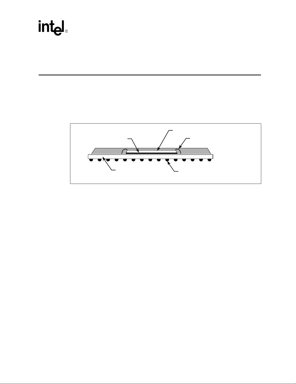
a copy of this document. The construction of the packages is shown in Figure 3.
Figure 3. Packaging Consideration s
Die Attach Epoxy
Polyimide Dielectic
Die
Wirebond
Eutectic Solder Balls
A9196-02
®
Design Guide 17
Page 18

Intel® 31244 PCI-X to Serial ATA Controller
®
31244 PCI-X to Serial ATA Controller Package
Intel
3.1 Sig na l Pin Descriptions
The signal pin descriptions for the GD31244 are provided as a reference. A complete list is also
available in the Intel
®
31244 PCI-X to Serial ATA Controller Datasheet.
Tab le 3. Serial ATA Signals Pin Descriptions
Name Description
TX0P, TX0N,
TX1P, TX1N,
TX2P, TX2N,
TX3P, TX3N
RX0P, RX0N,
RX1P, RX1N,
RX2P, RX2N,
RX3P, RX3N
CLKOUT OUTPU T - LVTTL: This is connected to one sid e of the 37.5 MHz crystal.
CLKIN
CLKO Buffered output of the 37.5 MHz clock.
RBIAS
CAP0, CAP1
LED0, LED1,
†
LED2
, LED3
† LED2 and LED3 are dual purpose pins. Refer to Table 7.
OUTPUT - Differential High-Speed Outputs: These are the differential serial outputs for
each channel. When disabled, these outputs are drive n to their DC-Bias point.
INPUT - Differential High-Speed Inputs: These are the differential serial inputs for each
channel.
INPUT - LVTTL: This is the reference clock input for the clock multiplier unit at 37.5 MHz. It
may be connected to either an external clock source or one side of a crystal.
INPUT - ANALOG: This pi n i s p ul l -down t o g rou nd w ith a 10 00Ω, 1% resistor in order to set
the internal termination resistors to 1000 Ω.
Analog: An external 0.1 µF (+/- 10%) capacitor is connected between these pins to set the
Clock Multiplier PLL loop filter response.
OUTPUT - LVTTL: These are the Activity LED outputs for channel 0, channel1, channel 2
†
and chan nel 3 (active LOW with 10 mA maximum sink capability).
18 Design Guide
Page 19

®
31244 PCI-X to Serial ATA Controller Package
Intel
Table 4. PCI-X Bus Pin Descriptions (Sheet 1 of 2)
Name Description
CAP2, CAP3
P_ACK64#
P_AD[63:0]
P_C/BE[7:0]#
P_CLK All PCI bus signals are referenced to this clock.
P_DEVSEL#
P_FRAME#
P_GNT#
P_IDSEL
P_INTA#
P_IRDY#
P_PAR
P_PAR64
P_PERR#
P_REQ#
Analog: An external 0.015 µF (+/- 10%) capacitor is connected between these pins to set
the PCI PLL loop filter response.
BIDIRECTIONAL - LVTTL: Indicates that the device has positively decoded its address as
the target of the current access and the target is willing to transfer data using the full 64-bit
data bus.
BIDIRECTIONAL - LVTTL PCI Address and Data: The address and data lines are
multiplexed on these pins. A bus transaction consists of an address phase followed by one
or more da ta ph as es . P _AD[ 63 :56] co nt ai ns t he mos t sig ni fic ant by te and P _AD [7: 0] con ta in
the lea s t significant byte.
BIDIRECTIONAL - LVTTL: Com man d and By te E nab le. The bus command and byte enable
signals are multiplexed on these pins. During the address phase, the P_CBE# lines define
the bus comma nd . Dur i ng th e da t a phas e, th e P_C BE # lin es ar e used as Byt e Enabl e s. The
Byte Enables are valid for the entire data phase and det ermine which byt e lanes carry
mean in gfu l da t a.
BIDIRECTIONAL - L V TTL wi th Pull-Up Resistor: Devi ce Sele ct. This signal is asserted by
the target once it has detected its address. As a bus master, the P_DEVSEL# is an input
signa l to th e I n tel
bus has been selected. As a bus slave, the GD31244 asserts P_DEVSEL# to indicate that it
has decoded its address as the target of the current tran saction.
BIDIRECTIONAL - LVTTL with Pull-Up Resistor: Cycle Frame. This signal is driven by the
current master to indicate the beginning and duration of a transaction. P_FRAME# is
asserted to indicate the start of a transaction and de-asserted during the final data phase.
INPUT - LVTTL. Grant: This signal is asserted b y the bus arbiter and indicates to t he
GD31244 that access to the bus has been granted. This is a point-to-point signal and every
mast er ha s its ow n GN T# .
INPUT - LVTTL. Initializati on Dev ice Select: This signal is used as a chip select during
PCI-X conf i gur at ion r ea d an d writ e tra ns act i on s. Thi s si gn al is pro vi ded by the ho st in PC I-X
systems.
OUTPUT - Open Drain Interrupt A: This signal is used to request an inter rupt by the
GD31244. This is an active low , level triggered interrupt signal.
BIDIRECTIONAL - LVTTL with Pull-Up Resistor: Initiator Ready. This signal indicates the
bus master ability to complete the current data phase and is used in conjunction with the
target ready (P_TRDY#) signal. A data phase is complet ed on any clock cycle where both
P_IRDY# and P_TRDY# are asserted LOW.
BIDIRECTIONAL - L V T TL: Parity. Pa rit y i s e ven ac ross P_ AD[3 1: 0] and P _CB E[ 3: 0]# li ne s.
It is stable and valid one clock after the address phase. For data phases, P_PAR is stable
and vali d one clock after either P_IRDY# is asserted on a write or P_TRDY# is asserted on
a read.Once P_PAR is valid, it remains valid until on e clock after th e completion of th e
current data phase. The master drives P_PAR for address and write data phases; and the
target, for read data phases.
BIDIRECTIONAL - LVTTL: Parity for 64-bit Accesses. Parit y is ev en ac r oss P_A D[ 63 :0 ] an d
P_CBE[7:0]# lines. It is stable and valid one clock after the address phase. For data phases,
P_PAR64 is stable and valid one clock after either P_IRDY# is asserted on a write or
P_TRDY# is asserted on a read.Once P_PAR64 is valid, it remains valid until one clock after
the comple ti on of th e cur re nt dat a ph as e. The mas t er dr i ves P_PAR64 for addr e ss a nd wri te
data ph ases; and the target, for read data phases.
BIDIRECTIONAL - LVTTL with P ull- Up Resistor: Parity Error. This signal is used to report
data p arity errors dur ing all PCI-X t ransactions except a Special Cycle. This signal is
asse rt e d tw o cl oc k cy cles afte r th e err o r was detecte d by th e de vi c e re c ei ving data. Th e
minimum duration of P_PERR# is one clock for each data phase where an error is detected.
A device cannot report a parity error until it has claimed the access by asserting
P_DEVSEL# and completed a data phase.
OUTPUT - LVTTL. Request: This signal indicates to the bus arbiter that the GD31244
desires use of the bus. This is a point-to-point signal and every bus master has its own
P_REQ#.
®
31244 PC I- X to ser ial ATA co nt ro ll er i nd ic at ing w h ethe r any d evi ce on the
Intel® 31244 PCI-X to Serial ATA Controller
Design Guide 19
Page 20
Intel® 31244 PCI-X to Serial ATA Controller
®
31244 PCI-X to Serial ATA Controller Package
Intel
Tab le 4. PCI-X Bus Pin Descriptions (Sheet 2 of 2)
Name Description
P_REQ64#
P_RST#
P_SERR#
P_STOP#
P_TRDY#
TEST0 INPUT - LVTTL: Test input. Set LOW for normal operation.
TOUT OUTPUT - T est pin. Do not use.
BIDIRECTIONAL - LVTTL: Indicates the attempt of a 64-bit transaction on the PCI bus.
When the target is 64-bit capable, the target acknowledges the attempt with the assertion of
P_ACK64#.
INPUT - LVTTL Reset: This signal is used to place PCI-X registers , sequencers, and
signal s into a consistent state. When P_RST# is asserted, all PCI-X output signals are
tri-stated.
OUTPUT - Open Drain with Pull-Up Resistor: System Error. This signal is used to report
address parity errors. When an error is detected, P_SERR# is driven LOW for a single
PCI-X clock.
BIDIRECTIONAL - LVTTL with Pull-Up Resistor: Stop. This signal is driven by the targe t
to indicate to the initiator that it wishes to stop the current transaction. As a bus slave,
P_STOP # is dr i ven by the GD 31 244 t o i n for m t he bu s ma st er t o stop t he curr e nt t r ansac ti o n.
As a bus master, P_ST OP# is received by the GD31244 to stop the current transaction.
BIDIRECTIONAL - LVTTL with Pull-Up Resistor: Target Ready. This signal indicates t he
selected device’s ab ility to complete the current data phase and is used in conjunction with
P_IRDY#. A data phase is completed on any clock cycle where both P_IRDY# and
P_TRDY# are asserted LOW.
Tab le 5. Configuration Pin Descriptions
Name Type Description
32BITPCI# INPUT
DPA_MODE# INP UT
SSCEN INPUT Tie this pin to GND.
Tab le 6. JTAG Pin Descriptions
Name Description
TDO
TDI
TCK
TMS
TRST#
TEST DATA OUTPUT: is the serial output pin for the JTAG feature. TDO is dri v en on the
falling edge of TCK during the SHIFT-IR and SHIFT-DR states of the Test Access Port. At
other times, TDO floats. The behavior of TDO is in dependent of P_RST#.
TEST DATA INPUT : is the serial input pin for the JTAG feature. TDI is sampled on the rising
edge of TCK, during the S HI FT-IR and SHIFT-DR states of the Test Ac ce ss Por t. Thi s sig nal
has a weak internal pull -up to ensure proper operation when this signal is unconnected.
TEST CLOCK: is an input which provides the clocking function for the IEEE 1149.1
Boundary Scan T esting (JTAG). State info rmation and data are clocked into the component
on the rising edge and data is clocked out of the component on the falling edge.
TEST MODE SELECT: is an in pu t samp led at th e ri sin g ed ge of TCK to select the operation
of the test logic for IEEE 1149.1 Boundary Scan testing. This signal has a weak internal
pull-up to ensure proper operation when this signal is unconnected.
TEST RESET: an input that asynchronously resets the Test Access Port (TAP) controller
function of IEEE 1149.1 Boundary Scan Testing (JTAG). This signal has a weak internal
pull-up.
Pin number A2. This pin control s the state of the “64 bit device” status
bit 16, in the PCI-X Status Regi ster. When pulled down, reports a 0, a
32-bit bus. When pulled up, reports 1, a 64-bit device.
INPUT - LVTTL: When HIGH or open, selects Master/Slave Mode for
software compatibility. When LOW, selects Master-Master mode for
high performance.
20 Design Guide
Page 21

®
Intel
Table 7. Serial ROM Interface Pin Descriptio ns
Name Description
Intel® 31244 PCI-X to Serial ATA Controller
31244 PCI-X to Serial ATA Controller Package
SDI
SDO (LED3)
SCLK (LED2)
SCS#
INPUT - LVTTL with Pull Up: Connects to the serial data output (SDO) of the Serial ROM.
Customers are recommended to add pads for both a pull-up and a pull-down resistor for
possible use in the future.
OUTPUT - LVTTL: Connects to the serial data input (SDI) of the Serial ROM. This is also
the ac tivity LED output for Channel 3 when all four LEDs are activated (active LOW).
OUTPUT - LVTTL: Connects to the clock input (SCLK) of the serial ROM. This is also the
acti vity LED output for Channel 2 when all four LEDs are activated (active LOW) .
OUTPUT - LVTTL with Pull Up: Connects to the chip select input (SCS#) of the Serial
ROM.
Table 8. Power Supply Pin Descriptions
Name Description
OUTPUT: This is the reg ul at ed 1 . 8V supply ge ner at ed i nt ern al ly. Bypa ss wit h 0.1 a nd 1 0µF
capacitors.
V18A, V18B
V
CC5REF
VA0 , VA1
V
SS
V
CC
V
IO
, V
V
CC0
V
, V
CC2
V18A and V18B are each outputs of internal voltage regulators. They need to be separately
bypassed to ground with 0.1 and 10 µF capacitors separately, they must not be connected
together.
Voltage Clamp I/O: In 5 V tolerant systems, this is connected to a 5 V supply. In 3.3 V
powere d systems this is connected to 3.3 V. In PCI add-in cards, this is normally connected
to I/O Power (10 A, 16 A, 19 B, 59 A and 59 B). The user must ensure that the value of
V
the GD31244 not just PCI inputs. For example, when the Serial ROM device is 5 V I/O this
pin must be 5 V regardless of the PCI bus.
2.5 V Analog Power Supply: Separate filtering is recommended. VA0 supplies the PCI
PLL. VA1 supplies the CMU.
Ground.
2.5 V Digital Logic Power Supply.
3.3 V PCI I/O Power Supply.
,
CC1
2.5 V High-Speed I/O Power Supply for each channel.
CC3
is hig h enou gh t o ensu r e c ompli an ce to t he V
CC5REF
speci fic ati o n on ev ery i n put to
IH(MAX)
3.1.1 VA0, VA1 (V
CCPLL
) Pin Requirements
To reduce clock skew, the VA0 and VA1 balls for the Phase Lock Loop (PLL) circuit are each
isolat ed o n the pac kag e. The lowpa s s fi lter, as shown in Figure 2, reduces noise induced clock ji tt er
and its effects on timing relationships in system designs. The 22 µF bulk capacitors must be low
ESR solid tantalum and the 0.1 µF ceramic capacitor must be of the type X7R. The node
connecting VA0 and VA1, must be as short as possible.
Design Guide 21
Page 22
Intel® 31244 PCI-X to Serial ATA Controller
®
31244 PCI-X to Serial ATA Controller Package
Intel
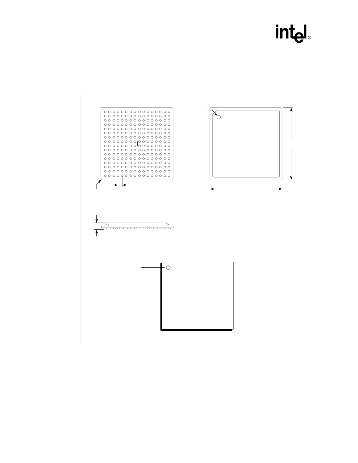
3.2 Package/Marking Information
The package is marked wit h three lines of text as shown in Figure 4. (The figure is not to scale.)
Figure 4. Package Information: 256-pin PBGA
12
1416
10
8
11
13
15
This page left intentionally blank.
3x 0.50 R
1.0 mm, Typ
BOTTOM VIEW TOP VIEW
13254769
A
B
C
D
E
F
G
H
J
K
L
M
N
P
R
T
Pin A1
Indicator
17mm
17mm
2.06 ± 0.3
SIDE VIEW
Pin A1 Identifier
Part Number Package Suffix
Date Code
Intel® 31244 XX
#### AAAA
Lot Tracking Code
A9626-02
22 Design Guide
Page 23
3.3 Ball Map By Function
Figure 5 shows the 544 BGA pins mapped by pin function. This diagram is helpful in placing
components aroun d the GD31244 for the layout of a PCB. To simplify routing and minimize the
number of cross traces, keep this layout in mind when placing components on your board. Name
signals, by desig n, are located on the PBGA package to simpl ify signal routing and s ys tem
implementation.
Figure 5. PB GA M apped By Pin Func ti on
1 2 3 4 5 6 7 8 9 101112 131415 16
32BIT
VSS
A A
B B
VCCREF VSS VSS TXOP RX0N TX1P RX1N VSS TX2P RX2N TX3P RX3N VSS VSS VCCREFVA1
LED3 TX0N RX0P TX1N RX1P CAP0 CAP1 TX2N RX2P TX3N RX3P CLKIN CLKOUT VSS
PCI#
LED2 P_AD32VCC
C
D D
E E
F F
G G
H H
J J
K K
L L
M M
N N
P P
R
T T
SCS# VSS VCC0 VCC1 VSS VSS VSS VSS TDO
VSS P_RST# P_INTA# VSS LED0 MS_DA SSCEN VSSVCC TRST# TCK VSS P_AD33
P_REQ# P_AD31 P_GNT# CLKO SDI LED1 TOUT TEST0 RBIAS TDI TMS P_AD36 P_AD35 VI0 P_AD34VIO
VIO
VSS
P_AD28 VIO P_AD29 P_AD30
P_AD25 VSS P_AD26 P_AD27
P_AD23 P_IDSEL P_CBE3 P_AD24 P_AD46 P_AD45 VIO P_AD44
P_AD19 P_AD20 P_AD21 P_AD22
P_AD18 VSS VCC VCC
V18A VIO
P_
TRDY#
P_
SERR#
P_
PERR#
P_PAR VSS P_AD15 VIO
VSS P_CBE1 P_AD14 VSS
12345678910111213141516
P_
IRDY#
P_
P_AD16
DEVSEL#
VSS
P_CBE2 VCCREF
P_
VSS P_AD13
STOP#
PCI-X Interface Pins
SERDES section
VIO
VIO
VIO
VIO
VIO
P_AD17
P_
VIO
FRAME#
P_AD12
P_AD11 P_CBE0 VSS P_CLK VSS VSS
P_AD10
P_AD9
VIO 3.3V
VSS
VSS VSS VSS VIO
VSS VSS VSS VSS
VSS
VSS VSS VSS VSS VSS VSS
VSS VSS VSS VSS VSS VSS
VSS VSS VSS VSS VSS
VSS VSS VSS VSS
VIO
VIO VIOVIO
VCCREF
P_AD8
VIO P_AD6 VA0 VSS P_AD3 VIO P_CBE6
P_AD7 P_AD5 CAP3 CAP2 P_AD2
VCC is 2.5V
JTAG Section
VCC2VSS VCC3VSS
VCC
VSS VSS
VSS P_AD4
VIO
VCCREF
VSS VIO
VSS
VSSVSS
VIO
P_AD1
P_
REQ64#
P_
ACK64#
P_AD39 P_AD38 VSS P_AD37
P_AD43 P_AD42 P_AD41 P_AD40
VIO
P_AD49 P_AD48 VSS P_AD47
VIO
VCC VCC P_AD51 P_AD50
VIO
P_AD53 P_AD52 VSS V18B
VIO
VIO
P_AD0
P_CBE7
P_CBE5
VSS VIO VCCREF
P_AD54
VCCREF P_AD57
P_CBE4 VSS P_AD59
P_AD63 VSS
VIO
VSS P_AD62 P_AD61
P_
VSS
PAR64
P_AD56 P_AD55
P_AD58
P_AD60
VSS
B0419-02
C
R
Design Guide 23
Page 24

Intel® 31244 PCI-X to Serial ATA Controller
®
31244 PCI-X to Serial ATA Controller Package
Intel
This page left intentionally blank.
24 Design Guide
Page 25

Intel® 31244 PCI-X to Serial ATA Controller
Rout ing Gu idelines
Routing Guidelines 4
This chapter provi des routing guidelines for layout and design of a printed circuit board using the
GD31244. The high-speed clocking required when de s igning with the GD31244 requires special
attention to signal integrity. In fact, it is highly recommended that the board design be simulated to
determine optimum layout for signal integrity. The information in this chapter provides guidelines
to aid the designer with board layout. S everal factors influe nce the signal integrity of a GD31244
design. These factors include:
• power distribution • decoupling
• minimizing cros st alk • layout conside r ations when routing the SATA bus
4.1 General Routing Guidelines
This section deta ils general routing guidelines for connecting the GD31244. The order in which
signals are routed varies from desi gner to designer. Some designers prefer to route a ll clock signals
first, while others prefer to route all high-speed bus signals first. Either order may be used,
provided the guidelines listed here are followed.
Route the GD31244 address/data and control si gnals using a da isy chain topology. This topology
assumes that no stubs are used to connect any devices on the net. Figure 6, shows two possible
techniques to achieve a stubless trace. When it is not possible to apply one of the se two techniques
due to congestion, a very short stub is allowed - do not exceed 250 mils.
Note: A rule of the thumb for stub trace length is to make sure that the stub length is less than or equal to
the one-quarter of the signal transition.
Example:
• Nominal trace velocity To = 190 ps/in
• Typical signal slew rate = 2 V/ns
• Low-to- H ig h Voltage differential (0.3V
• Rise Ti me T
=.66 V *(1 ns/2 V) = 330 ps
R
to 0.5 VCC) =0.66 V
CC
• Equivalent Distance = 330 ps/T o = 1. 74in
• Stub length less than 1/4 of the length =0 .44 in
Figure 6. Examples of Stubless and Short Stub Traces
Stubless Short Stub
<250 Mils
A7690-01
Design Guide 25
Page 26

Intel® 31244 PCI-X to Serial ATA Controller
1
Routing Guidelines
4.2 Crosstalk
Crosstalk i s ca used by capa citi ve and ind uctive c oupling bet ween sign al s. Cr osst alk i s compos ed of
both backwar d and for ward cross talk compon ents. B ackward crosst alk c reate s an indu ced sign al on
victim network that propagates in the opposite direction of the aggressor signal. Forward crosstal k
creates a signal that propagates in the same direction as the aggressor signal.
Circuit board a nalysis software is used to analyze your board layo ut for crosstalk problems.
Examples of 2D analysis tools inc lude Parasitic Parameters from ANSOFT
*
Design
. Crosstalk prob lems occur when circuit etch line s run in parallel. When board analysis
software is not available, the layout maintain s minimum spacing between parallel circuit signals
lines.
• A general guideline to use is, that space distance between adjacent signals be a least 3.3 times
the distance from signal trace to the nearest return plane. The coupled noise between adjacent
traces decreases by the square of the distance between the adjacent traces.
• It is also recommended to sp ec ify the height of the above reference plane when laying out
traces and provide this parameter to the PCB manufacturer. By moving trac es closer to the
nearest reference plane, the coupled noise decreases by the squ are of the distance to the
referen ce p la n e.
Figure 7. Crosstalk Effects on Trace Distance and Height
P
H
aggressor victim
Reference Plane
• Avoid slots in the ground plane. Slots inc r eases mutual inductance thus incre as ing crosstalk.
• Make sure that ground plane surrounding connector pin fields are not completely cleared out.
When this area i s compl etely clea red out, aro und the c onnect or pins , all the ret urn curre nt must
flow togeth er around the pin field increasing crossta lk. The preferred method of laying out a
connector in th e GND laye r is shown in Figure 8B.
*
and XFS from Quad
Reduce Crosstalk:
- Maximize P
- Minimize H
A9259-01
Figure 8. PCB Gr ound Layout Around Connectors
Connector
Connector Pins
GND PCB Layer
A. Incorrect method B. Correct method
A9260-0
26 Design Guide
Page 27

4.3 EMI Considerations
It is highly recommended that good EMI design practices be followed when desi gning with the
®
31244 PCI-X to serial ATA controller.
Intel
• To minimize EMI on your PCB a useful technique is to not extend the power planes to the
edge of the board.
• Another technique is to surround the perimeter of your PCB layers with a GND trace. Thi s
helps to shield the PCB with grounds minimizing radiati on.
The below link may provide some us eful general EMI guidelines considerations:
http://developer.intel.com/design/auto/mcs96/applnots/272673.htm
Intel® 31244 PCI-X to Serial ATA Controller
Rout ing Gu idelines
Design Guide 27
Page 28

Intel® 31244 PCI-X to Serial ATA Controller
Routing Guidelines
4.4 Power Distribution and Decoupl ing
Have ample decoupling to ground, for the power pl anes, to minimize the effects of the switching
currents. Three types of decoupling a re: the bulk, the high-frequency ceramic, and the inter-plane
capacitors.
• Bulk capacitance consist of el ectrolytic or ta ntalum capacitors. These capacitors supply large
reservoirs of charge, but they are useful only at lower frequenc ies due to lead inductanc e
effects. The bulk capacitors may be located anywhere on the board.
• For fast switching currents, high-fre quency low-inductance ca pacitors are most effective.
Place these ca pac itors as close to the device being decoupled as possible. This minimizes the
parasitic resistance and inductance associated with board traces and vias.
• Use an inter-plane c apacitor between power a nd ground planes to reduce the effective plane
impedance at high frequencies. The general guideline for placing capacitors is to plac e
high-frequ ency ceramic capacitors as close as possibl e to the module.
4.4.1 Decoupling
Inadequate high-freque ncy decoupling re su lts in intermittent and unreliable beh avior. A general
guideline recommends that you use th e largest easily available capacitor in the lowest inductance
package.
4.4.1.1 Intel® 31244 PCI-X to Serial ATA Controller Decoupling
It is rec om me nded that to decouple the VCC 2.5 V, use at least t welve 0.1 µF capacitors in as close
proximity to the GD31244 VCC pins as possible. When feasible, locate these ca pacitors on the
back of the board, close to the GD31244 VCC ball.
28 Design Guide
Page 29

4.5 Trace Impedance
e
All signal layers require controlled impedance of 50 Ω +/- 15%, microstrip or stripline w here
appropriate, unless otherwise specified. Select in g the appropriat e boa rd st ack-up to minimize
impedance variations is very important. When calculating flight times, it is important to consider
the minimum and m aximum t race impedanc e bas ed on th e swit chi ng neig hbori ng tr aces. Use wider
spaces between traces, since this may minimize trace-to-trace coupling, and reduce cross talk.
All recommendat ions described in this document assume a T
otherwise specified. When a different stack up is used the trace widths must be adjusted
appropriately. When wider traces are used, the trace spacing must be adjusted accordingly
(linearly).
It is highly recommend ed tha t a 2D Field Solver be used to design the high-speed traces. The
following Impedance Calculator URLs pro vide approximations for the trace impe dance of various
topologies. They may be used to generate the starting point for a full 2D Field solver.
http://emclab.umr.edu/pcbtlc/
http://www.westak.com/techcenter/imped/
The following websit e link provides a useful basic guideline for calcul ating trace parameters:
http://www.ultracad.com/calc.htm
Note: Using stripline transmission lines may give better results than microstrip. This is due to the
difficulty of precisely controlling the dielectric constant of the solde r mask, and the difficulty in
limiting the plated thicknes s of microstrip conductors, which may substantially increase cross-talk.
4.5.1 Differ e nt ial Impe da nc e
The Serial ATA standard defines a 100 ohms differential impedance. This section provide s some
basic background information on the differentia l impedance calculations. In the cros s section of
Figure 9 shows the cross section of two traces of a differential pair .
Figure 9. Cross Section of Differential Trace
5mil50Ω signal trace, unless
wid
Ground reference plan
To calculate the coupled impedance requires a 2x2 matrix. The diagonal val ues in the matrix
represent the impedance of the traces to ground and the off-diag onal values provide a measu re of
how tightly the traces are coupled. T he differential impedance is the val u e of the line-to-l ine
resistor terminator that optimally terminates pure diff erential signals. The two by two matrix is
shown below as:
Example 1. Two-by-two Differential Impedance Matrix
Z11 Z12
Zo
=
Z21 Z22
Design Guide 29
Page 30

Intel® 31244 PCI-X to Serial ATA Controller
Routing Guidelines
For a symmetric trace Z11 = Z22, the differential impeda nce may be calcula ted from this equation:
Z
differential
For two traces to be symmetric, they must have the same width, thickness and height above the ground
1
With the traces terminated with the appropriate differential, impedance ringing is minimized.
plane.
= 2(Z11-Z12)
1. “Terminatin g Differe nti al Signals on PCBs ”, Ste ve Kauf er and Kelee Crisa fu lli, Prin te d Circu it D esi gn, Ma rc h 1999
30 Design Guide
Page 31

®
31244 PCI-X to Serial ATA Controller Interface Ports
Intel
Intel® 31244 PCI-X to Serial ATA Controller
Intel® 31244 PCI-X to Seri al ATA
Controller Interf ac e Ports 5
5.1 Serial ROM Interface
In add-in card applications, firmware may be downloaded to the syste m from a Serial EEPROM or
Serial Flash ROM, through the Serial ROM Interface. This industry standard, 4-pin interface,
allows any size of device, up to 128 Kbytes, to be connected to the Intel
ATA controller. This SPI int erfa ce was designed for compatibility with an ST Microelectronics*
M25P10-A or Atmel* AT25F1024 device. Two of the pins are dual purpose to sup port four LED
port activity indicators. This four pin interface is defined as foll ows:
1. SDI INPUT: Connects to the serial data output (S O) of the Serial EEPROM. Data is shifted
out of the EEPROM on the falling edge of SCLK. Customers are recom mended to add pads
for both a pull-up and a pull-down resistor for possib le use in the future.
2. SDO OUTPUT: Connects to the serial data input (SI) of the Serial EEPROM. Data is latched
into the Serial EEPROM on the rising edge of SCLK. This is als o the activity LED output for
Channel 3 when all four LEDs are act ivated (active LOW).
3. SCLK OUTPUT: Connects to the clock input (SCK) of the Serial EEPROM. This is also the
activity LED output for Channel 2 when all four LEDs are activated (active LOW).
®
GD31244 PCI-X to serial
4. SCS# OUTPUT: Conne cts to the chip selec t input (CS#) of the Serial EEPROM.
5.2 JTAG Interface
An IEEE 1149.1 compatible JTAG interface and boundary scan func tionality is provided to assist
on-board testing of the device. A BSDL test file is provided by Intel.
Design Guide 31
Page 32

Intel® 31244 PCI-X to Serial ATA Controller
®
31244 PCI-X to Serial ATA Controller Interface Ports
Intel
5.3 PCI-X Interface
The 64-bit, 133 MHz PCI-X interface is fully compliant with the PCI Local Bus Specification,
Revision 2.2 and the PCI-X Ad dendum to the PCI L oc al Bus Sp ecific a t io n, Revision 1.0a. The
PCI-X bus supports up to 1064 Mbytes/s transfer rate of burst data. The GD31244 is backwards
compatible with 32-bit/33 MHz, 32-bit/66 MHz and 64-bit/66 MHz operation. The PCI logic
supports Plug -n-P lay operation, which allows hardware and firmwar e to re solve all setup conflicts
for the user. The GD31244 supports both slave and master data transfe rs. The devices res ponds to
the following bus cycles as a slave:
• I/O Reads • Configuration Read
• I/O Writes • Configuration Write
• Memory Read Bus Cyc les
As a master, the GD31244 responds to:
• Single Memory Reads • Line Memory Reads
• Multiple Memory Reads • Memory Writes
During sys tem initialization, the Configuration Manager of the host system reads the configuration
space of each PCI-X device. Aft er har dware r eset, the GD31244 only responds to PCI-X
Configuration cycles in anti cipation of being initialized by the Configuration Manager. Ea ch
PCI-X devic e is addressable individually by the use of unique IDSEL# signals which, when
asserted, indicate that a configuration read or write is occurring to this device. The Configuration
Manager reads the setup registers of each device on the PCI-X bus and then, based on thi s
informatio n, assigns system resources to each supported function through Type 0 configuration
reads and writ es. Type 1 configuration cycles are i gnore d. This sche me allo ws the GD31244 and it s
external ROM to be relocated in the memory and I/O space. Interrupts, DMA Channels and other
system resources may be reallocated appropriately.
32 Design Guide
Page 33

®
31244 PCI-X to Serial ATA Controller Interface Ports
Intel
5.4 Serial ATA Interface
Four 1.5 Gbits/s Serial ATA ports are located on the GD31244, to support point-to-point
connectivi ty to disk drives, CDROMs, DVD ROMs or any other Ser ial ATA target device. Each
port is compliant with the “Serial ATA: High speed Serialized AT Att achme nt Specification,
Revision 1.0e. High-speed diff erential duplex serial lines se nd 8B/10B encoded data to and from
the GD31244 and the target at a maximum raw data rate of 1.2 Gbits/s (150 Mbytes/s). Copies of
the targets Task File Registers are maintained on the GD31244 and transferred as needed to the
target. The Serial ATA protocol is software compatible with all existing operating systems that
support ATA devices, however, perfo rmance and reliability are improved since all data is CRC
checked.
5.4.1 Direct Port Access (DPA)
The SATA Dire ct Port Access architecture allows for independent control of the SATA devices.
Unlike ATA master/slave con f iguration where only one drive may operate at a time, DPA allows
multiple drivers to be accessed concurrently. In addition, each port supports its own DMA cha nnel
allowing each port to transfer data independently (between a device and memory).
The DPA mode does change the register layout from PCI IDE. Therefore, legacy device drivers do
not support this mode. DPA requires the registers (incl uding the Command Block , Control Block,
DMA, and SATA superset) for each drive is available at all times. Instead of using I/O space, these
registers are mapped to a single 4 KB block. Each port has 512 KB; the remaining 2 048KB are for
the common port registers. The 4 KB block is mapped using one PCI BAR register.
Intel® 31244 PCI-X to Serial ATA Controller
5.4.2 Ext en de d Voltage Mode
The SATA voltages were designed primarily for a cable connection to the hard drives. In certain
applications , s uch as NAS/SAN enclosures, the hard disk drives (HDD) are conne cted to a
backplane, not a cable (typically in desktop systems). Due to the frequency of the SATA interface,
the backplane cre ates a significant attenuation of the SATA signals. In an effort to simplify system
designs, the GD3124 4 of fers an extended voltage range to help all eviate this issue . T his extended
voltage range allows standard SATA HDD to be used with SATA backplanes.
The firmware may be place int o the Exte rnal Voltage Mode by setting bit 14 in PHY Configuration
Register Address 140H to 1. This forces the firmware to operate with this extended vol tage range.
Table 9. Normal Volta ge Mode
Parameter Description Minimum Maximum Units
∆
V
OUT
∆
V
IN
Table 10. Extended Voltage Mode
Parameter Description Minimum Maximum Units
∆
V
OUT
∆
V
IN
TXx output differential peak-to-peak voltage swing 400 600 mVp -p
RXx input dif ferential peak-to-peak voltage swing 325 600 mVp-p
TXx output differential peak-to-peak voltage swing 800 2000 mVp-p
RXx input dif ferential peak-to-peak volt age swing 175 2000 mVp-p
Design Guide 33
Page 34

Intel® 31244 PCI-X to Serial ATA Controller
3.3V
3.3V
3.3V
®
31244 PCI-X to Serial ATA Controller Interface Ports
Intel
5.4. 3 LED Interface
Serial ATA interfaces on disk drives do not include the traditional ATA output, which drives an
LED to indicate that the drive is active. The GD31244 compensates for this missing function by
adding four LED outputs , which sink 10 mA. In Master/Slave com patibility mode, LED0 goes
LOW to turn on an Activity LED, anytime there is activity on either Channel 0 or Channel 1.
Likewise , LED1 goes LOW to turn on an Activity LED, anytime there is activity on either
Channel 2 or Channel 3. These two outputs may be wire -ORed toge ther to use one LED for al l four
ports. During EEPROM tra nsfers, the LED function on SCLK and SDO is suspended. A buffer
may be required when the LEDs are located off-bo ard a nd an EEPROM is used.
When GD31244 is configure d in Dir ect Port Acce ss mode (DPA_MODE# is LOW), then each port
is assigned its own LED as follows:
• Port 0 on LE D0
• Port 1 on LE D1
• Port 2 on LE D2
• Port 3 on LE D3
During EEPROM transfers, the LED function on SCLK and SDO is suspende d. A buffer may be
required when the LEDs are loc ated off-board and an EEPROM is use d. Figure 10 shows a th e
common configurations of using the serial EEPROM in conjunction with the LEDs.
Figure 10. LED and Serial EEPROM Configurations
Serial EEPROM
SDO
SDI
SCS#
SCLK
LED0
LED1
4 LEDs
DPA Mode
No EEPROM
LED
LED
LED
LED
470W
3.3V
3.3V
3.3V
3.3V
SDO
SDI
SCS#
SCLK
LED0
LED1
B. Typi cal HBA:A. Server Application:
2 LEDs
Master/Slave Mode
EEPROM for Boot co de
LED
LED
SI
SO
CS#
SCK
470W
3.3V
3.3V
Serial EEPROM
LED
LED
LED
LED
SI
SO
CS#
SCK
SDO
SDI
SCS#
SCLK
*
LED0
LED1
C. Typi cal HBA:
4 LEDs
Master/Slave or DPA Mode
EEPROM for Boot code
* Optional Buffers for off-board LEDs
470W
3.3V
3.3V
3.3V
3.3V
34 Design Guide
Page 35

5.4.4 Reference Clock Generation
A 37.5 MHz reference clock with a +/- 100 ppm accuracy is required for proper operati on of the
GD31244. This is generated from an external oscillator connected directly to the XI input.
Optionally, a 37.5 MHz crystal may be connected between the XI and XO pins with a 20 pF
capacitor from XI to ground and another from XO to ground. The following are th e crystal
characteristics:
• Frequency: 37.5 MHz +/- 100 ppm
• Mode: Fundamental
• Type: Parallel resonant
• ESR: 30 Ohms maximum
• Load Capacitance: 20 pF
• Shunt Capacitance: 7pF
• Drive Level: 500 mW maximum
• Recommended Vendor/Part Number: Fox Electronics, Part number: 278-37.5-8 (This is an
HC-49SD surface mountable package.)
Place the crystal near the GD31244 and isolated from noisy circuits as much as possible.
Design Guide 35
Page 36

Intel® 31244 PCI-X to Serial ATA Controller
®
31244 PCI-X to Serial ATA Controller Interface Ports
Intel
This page left intentionally blank.
36 Design Guide
Page 37

Intel® 31244 PCI-X to Serial ATA Controller
Printed Circuit Board (PCB) Methodology
Printed Circuit Board (PCB)
Methodology 6
This section provides a recommended guidelines for PCB stackup. A considerable part of the SI
analysis, is to identify and recommend the backplane stackup recommendations. This guideline
section is separated into two recomme ndations:
• GD31244 in normal mode, refer to Table 9.
• GD31244 in extended voltage mode for backplane designs, refer to Table 10.
The specifi ed impedance range for SATA is differential 100 +
SATA path:
15% ohms for all components of the
• backplane • cables
• motherboard • connectors
Table 11 defines the starting point for possible stackups.
The assumption is that GD31244 is i mplemented with normal 60 ohm guidelines, with the primary
applicati on being standard desktop PC.
Design Guide 37
Page 38

Intel® 31244 PCI-X to Serial ATA Controller
Printed Circuit Board (PCB) Methodology
6.1 Intel® 31244 PCI-X to Serial ATA Controller Normal Mode (s tandard SATA driver)
This section provides recommendations for the GD31244 running in the standard SATA mode.
Figure 11 shows a standard SATA setup with the GD31244 connected to trace on the motherboard.
This trace te rmi nates with a connector. The SATA cable conne cts to the SATA motherboard cable
with the other end connecting to connector on the hard drive. The traces from the SATA hard drive
connector connect to the SATA interface IC on the hard drive.
Figure 11. Intel
®
31244 PCI-X to Serial ATA Controller Connection Scheme - Normal Mode
®
Intel
31244
Traces
Tab le 11. Normal Voltage Mode
Parameter Routing Guideline
Single Ended Trace I m pedance Mic rostrip stackup
Refere nce Plane ground
Impeda nc e 100 ohms diffe r en tia l im pedance
Trace Thickness 1 . 4 mi l
Trace Width 5 mil
Intra Pair Trace Spacing 7 mil
Pair to Pair
Trace Spacing
Trace Length 2” to 5”
Trace Leng t h Ma tc hi ng 100 mils
Cable Length 1 meter
Hard drive PCB Length from connector to SATA
interface IC.
Vias
MB
Conn.
Cable
HD
Conn.
SATA IC
Traces
B0423-02
20 mil minimum
1”
Minimize number of vias (none preferred). Each
channel in the pair has an equa l number of vias.
38 Design Guide
Page 39

Intel® 31244 PCI-X to Serial ATA Controller
Signal
l
Printed Circuit Board (PCB) Methodology
6.1.1 Intel® 31244 PCI-X to Serial A TA Controller HBA Stackup
The below stackup in Figure 12, shows the layer topology tha t is used in the HBA customer
reference board. The first layer, Layer 0 is a signal layer, the second layer, La yer 1 is ground, the
third layer, Layer 2 is 2.5 V plane with some traces, the fourth la yer, Layer 3 is the 3.3 V plane
with some traces, the fifth layer, Layer 4 is ground and the sixth layer Layer 5 may be used for
additional signals.
Figure 12. Intel
®
31244 PCI-X to Serial ATA Controller HBA Stacku p
Layer 0
Layer 1
Layer 2
Layer 3
Layer 4
Layer 5
6.2 Extended Voltage Mode
This section details the recommendation for backplane applications with GD31244. The driver
characteristics for th is mode ar e listed in Table 10.
This Extende d Voltage Mode was im plemented because the as is, the SATA spe c driver parameters
are insufficient to drive a backpl ane interconnect . Th e ‘min’ driver has been modified, and this
analysis assumes that the min driver meets this criteria:
Note: All changes have been made to GD31244 only. The SAT A hard dis k drive has been assumed to
conform to the spec.
Prepeg
Vss-GNC
Signal, V
Thick Prepreg
V
Vss -G ND
Prepeg
Signal
3.3
2.5,
, Signal
Signa
New ‘min’ corner driver specifications:
• 50 0mV peak-to-peak amplitude vs. 400mV of spec
• Total jitter must be < 0.35 UI vs. 0.45 UI of spec (@DRV pin)
• Edge rate must be >= 0.3 UI vs. 0.41 UI of spec
• Everything not li sted is same as SATA spec
• Attenuation sche m e is use d only for GD31244 write dif ferential pairs TX lines not on RX
lines.
The ‘min’ rec eiver has been modified, and this solution space is assuming the GD31244 receiver
meets th is criter i a:
New ‘min’ corner receiver specificati ons :
• 220 mV peak-to-peak amplitude vs. 325 mV of specification
Design Guide 39
Page 40

Intel® 31244 PCI-X to Serial ATA Controller
Printed Circuit Board (PCB) Methodology
• Jitter tolerance (TJ) must be >= 0.7 UI vs 0.62 UI of spec (@RCV pin)
• Slowest edge rate as sumed
• Used only for GD31244 reads
• Read eye was guardbanded by 10 mV to allow for crosstalk
6.2.1 Backplane Topologies
This analysis looks at two backplane interconnection topologies. These two backplane topologies
are divided i nto the t wo cate gori es for the re ad RX line s and wri te TX li nes. Thes e are shown in the
figures be low. Figure 13a shows the GD31244 motherboard connecting through a connector to a
backplane with resistor attenuation for write topologies. Figure 13b shows the GD31244
motherboard connecting through a ribbon cable to a backplane for write topologies with r esis tor
attenuation. The resistor termination for Figure 13 is R1/R2 = 15 ohms/150 ohms 5% resistors
provided 50 ohm impedance.
The Figure 14a shows the read topology from the SATA hard drive to a connector to through the
backplane connector to the motherboard connec ting to the GD31244 RX differential pins. In
Figure 14b shows the read topology from the SATA hard drive to a connecto r to through the
backplane connector through a ribbon cable to a motherboard connecting to the GD31244 RX
differential pins. Note that reads do not have the extra resistor termination.
This section provides an example target system topology for designing a GD31244-bas ed Serial
AT A system. The target system implementation is based on one or more GD31244 chips mounted
on the mother board and a backplane supporting 4 to 16 hot-plug SATA drives.
In the propo sed exampl e to polo gy covere d in thi s se ction the bac kpl ane is co nfig ured mecha nical ly
for either 3.5” x 1.0” or 2.5”x 0.75” form factor drives.
Figure 13. Write Backplane Topology
a. Write Backplane Topology
Package
®
Intel
31224
b. Write Backplane with Cable Topology
31224
Model
Package
Model
MB
MB
MB
MB
Connector
Cable
Connector
BP
BP
BP
BP
Connector
Connector
Connector
SD
SD
SD
SD
HDD
HDD
B0604-01
R1
R1
R1
R2
R1
R1
R1
R1
R2
R1
40 Design Guide
Page 41

Figure 14. Read Backplane Topology
a. Read Backplane Topology
®
Intel
31224
b. Read Backplane with Cable Topology
31224
Package
Model
Package
Model
Intel® 31244 PCI-X to Serial ATA Controller
Printed Circuit Board (PCB) Methodology
MB
MB
Connector
MB BP
MB BP
Cable
Connector
BP
BP
Connector
Connector
Connector
SD
SD
SD
SD
HDD
HDD
B0605-01
Design Guide 41
Page 42

Intel® 31244 PCI-X to Serial ATA Controller
Printed Circuit Board (PCB) Methodology
6.2.2 Motherboard Stackup for Backplane Designs
The motherboard is supporting components in addition to GD31244, so an assumption is, desktop
PC requirements are domina te to ass ure the process or and memor y subsys tem may be im plem ented
with normal 60 ohm guidelin es.
Tab le 12. Motherboard Stackup, Microstrip
Variable Nomina l (mil) Toler ance Min (mil ) Max (mil)
Mask Th ic kn es s 0.8 +/- 0.2 0.6 1.0
Mask Er 3.6 3.6 3.6
Trace Hei gh t 4.0 +/- 0.3 3.7 4.3
Preg Er 4.15 +/- 0.55 3.6 4.7
Plane Thickness 1.4 +/- 0.2 1.2 1.6
Trace Thickness 1.4 +/- 0.4 1.0 1.8
Trace Width 5 mil +/- 1.5 3.5 6.5
Total Thickness 62.0 +/- 6.0 56.0 68.0
Tab le 13. Motherboard Micro stri p Param eters
Parameter Routing Guideline Notes
Motherboard La yo ut Micro strip
Single Ended Trace Im pe da nc e 5 5 +/ - 12 %
Differential Trace Impedance 100 ohms +/- 15%
Reference Plane ground
Trace Thickness 1.4 mil
Trace Width 5 mil
Intra Pair Trace Spacing 15 mil intra-pair to pair center-to-center
Pair-to-Pair Trace Spacing 55 mil pair to pair center-to-center
Trace Length 2” to 6”
Trace Length Matching 10 mi l Intra-pair matching
Vias 0
When possible , it is recommended that the designer us e stripline for the following reasons:
• Reduced skin effect r elative to microstrip
• Reduced forward cross talk
• Reduced jitte r through differential stackup and isolated power delivery
Minimi z e num ber of vias (none prefer r ed ) . Ea c h
channe l in th e pair ha s an equal numbe r of via s.
42 Design Guide
Page 43

Figure 15. Microstrip Stackup
10 mil
1.4 mil
1.4 mil
+
Er = 4.15
5 mil
-
Mask Er = 3.65
55 mil
0.8 mil
+
-
4 mil
B0424-01
Design Guide 43
Page 44

Intel® 31244 PCI-X to Serial ATA Controller
1
Printed Circuit Board (PCB) Methodology
6.2.3 Backplane Stripline Stackup
Figure 16 provides an example stackup that may be used to implement the backplane design. The
stripline shown in Figure 16 is impleme n ted with ground flood on both component and solder side
of the PCB. The dif ferent ial s tr ipline trace s are etc hed from the power a nd ground pl ane s. Note th at
this inf or ma tion is preliminary.
Tab le 14. Backplane Stripline Stackup
Parameter Routing Guideline Notes
Single Ended Trace Impedance 60 +/- 14% ohms
Differential impedance 100 +/- 15%
Reference Plane ground
Trace Thickness 1.4 mil
Trace Width 11.5 mil
Intra Pair Trace Spacing 29.7 mil intra-pair center-to-center (broadside coupled)
Pair to Pair
Trace Spacing
Trace Length 2” to 14”
Trace Length Matching 10 mils int ra-pair matching
R1 15 +/- 5% ohms
R2 150 +/- 5% ohms
60 mil
pair-to-pair, center-to-center for two adjacent
differential pairs
Required only for the write topology shown in
Figure13.
Required only for the write topology shown in
Figure13.
Figure 16. Stripline Stackup
.4 mil
Er = 4.66
49.5 mil
+ ++
29.7 mil
11.5 mil
– ––
17 mil
1.4 mil
Er = 4.66
1.4 mil
Er = 4.66
B0425-01
44 Design Guide
Page 45

Table 15. Backplane Stackup, Microstrip
Variable Nominal (mil) Tolerance Min (mil) Max (mil)
Mask Thickness 0.8 +/- 0.2 0.6 1.0
Mask Er 3.6 3.6 3.6
Trace Height 1.4 +/-0. 3 1.1 1.7
Preg Er 4.66 +/-0.55 3.6 4.7
Plane Thickness 1.4 +/-0.2 1.2 1.6
Trace Thickness 1.4 +/-0.4 1.0 1.8
Trace Width 11.5 +/-1.5 10 13
Total Thickness 70.0 +/-7.0 63.0 77.0
Table 16. Backplane Stackup, Offset Stripline
Variable Nominal (mil) Tolerance Min (mil) Max (mil)
Mask Thickness 0.8 +/- 0.2 0.6 1.0
Mask Er 3.6 3.6 3.6
Trace Height
Preg Er 4.15 +/-0.55 3.6 4.7
Plane Thickness 2.2 +/-0.2 1.2 1.6
Trace Thickness 1.4 +/-0.4 1.8 2.6
Trace Width 11.5 +/-1.5
Total Thickness 70.0 +/-7.0 63.0 77.0
1
Intel® 31244 PCI-X to Serial ATA Controller
Printed Circuit Board (PCB) Methodology
+/-0.3
6.2.4 Cable Interconnect With Backplane
Figure 14 provides the topology which uses a cable as an interconnect between the motherboard
and backplane.
Table 17. Cable Specification
Paramet er Routing Guid eli ne Notes
Characteris tic Z - Cable 100 ohms +/- 15%
Trace Leng th 1”-6”
Trace Matching 150 mil s
Design Guide 45
Page 46

Intel® 31244 PCI-X to Serial ATA Controller
Printed Circuit Board (PCB) Methodology
This page left intentionally blank.
46 Design Guide
Page 47

Intel® 31244 PCI-X to Serial ATA Controller
PCI-X Lay out Gu id el in e s
PCI-X Layout Guidelines 7
This section provides guideli nes for des igning with the Intel® 31244 PCI-X to serial ATA
controller PCI/PCI-X (PCI/X) bus interface in your application. This chapter is divided as follows:
• PCI/X voltage le vels
• clocking modes
• general layout guidelines
• layout guideli nes for the different slot configurations using PCI-X
7.1 PCI Voltage Levels
The Intel® 31244 PCI-X to seria l ATA controller does not support a 5 V PCI signaling interf ace, it
supports 3.3 V only. Supporting a 5 V PCI interface requires additi onal I/O level transl ation
circuitry. Table 18 is provided as a reference for the PCI/X signaling levels. A complete PCI-X
Addendum to the PCI Loc al Bus Speci fi cation, Revis ion 1. 0a may be foun d on t he www.pcisig.com
website.
Table 18. PCI/X Voltage Levels
Symbol Parameter Minimum Maximum Units
V
IL3
V
IH3
V
IL4
V
OL3
V
OH3
Input Low Voltag e (PCI-X) -0.5 0.35 V
Input High Voltage (PCI-X/PCI) 0.5 V
Input Low Voltage ( PC I) -0.5 0 .3 V
Output Low Voltage (PCI-X) 0.1 V
Output HIGH Voltage (PCI-X) 0.9 V
CC33VCC33
CC33
CC33
+ 0.5 V Voltage
CC33
CC33
Voltage
Voltage
Voltage
Voltage
Design Guide 47
Page 48

Intel® 31244 PCI-X to Serial ATA Controller
PCI-X Layout Guidelines
7.2 PCI/X Clock ing Modes
The Intel® 31244 PCI-X to serial AT A c ontro ller c lockin g modes for PC I-X and PCI bus are shown
in Table 19. At PCI bus reset, the Intel
P_IRDY#, P_TRDY#, P_STOP#, and P_DEVSEL# to determine the operati ng frequency for
PCI-X mode. When P_FRAME# is deas serted and P_IRDY# is deasserted (i.e., the bus is idle)
and one or more of P_DEVSEL#, P_STOP#, and P_TRDY# are asserted at the rising edge of
P_RST#, th e d ev i ce enters PC I -X mode (see Table 19). Otherwise, the device ent er s conventional
PCI mode. With conventional PCI mode, a low on M66EN determines the PCI bus is at 66 MHz.
Tab le 19. PCI-X Clocking Modes
Mode/CLK PCI/XCAP M66EN P_DEVSEL# P_STOP# P_TRDY#
PCI 33 MHz GND Deasserted Deasserted Deasserted Deasserted
PCI 66 MHz GND Asserted Deasserted Deasserted Deasserted
PCI-X 66 MHz
PCI-X 100MHz
PCI-X 133MHz
10 KΩ 0.01 µF
cap to GND
0.01 µF cap to
GND
0.01 µF cap to
GND
®
80321 I/O processor samples th e P_FRAME#,
N/A Deasserted Deasserted Asserted
N/A Deasserted Asserted Deasserted
N/A Deasserted Asserted Asserted
48 Design Guide
Page 49

Intel® 31244 PCI-X to Serial ATA Controller
7.3 PCI General Layout Guidelines
For acceptabl e signal int eg rity with bus spee ds up to 133 MHz it is important to PCB design layout
have controlle d impedance.
• Signal traces have an unl oaded impedance of 60 +/- 10% Ω.
• Signal trace velocity is roughly 150 – 190 ps/inch
The below list provides general guidelines used when routing your PCI bus signals:
• Avoid routing signals > 8”.
• All clock nets must be on the top layer.
• All 32-bit interface signals from the PCI edge fingers must be no longer than 1.5” and no
shorter than 0.75”.
• All 64-bit extension si gnal from the PCI edge fingers must be no longe r than 2.75” and no
shorter than 1.75”.
• CLK from the PCI edge finger must be 2.5” +/- 0.1”.
• P_RST# from the PCI edge finger must be no longer than 3.0” and no shorter than 0. 75”.
PCI-X Lay out Gu id el in e s
• The following signals have no length restrictions: INTA#, INTB#, INTC#, INTD#, TCK,
TDI, TDO, TMS and TRST#
Table 20 provides information on maximum lengths for rout ing add-on card signals.
Table 20. Add-on Card Routing Parameters
Parameter
CLK 2.4 2.6
P_AD[0 – 31] 0.75 1.5
P_AD[32 – 63] 1.75 2.75
P_RST# 0.75 3.0
Do not use more than one via for the primary PCI bus signa ls.
PCI-X
Minimum Maximum
Design Guide 49
Page 50

Intel® 31244 PCI-X to Serial ATA Controller
PCI-X Layout Guidelines
7.4 PCI-X Layout Guidelines For Slot Configurations
The PCI-X Addendum to the PCI Local Bus Specifi cation, Revision 1.0a recom mends the
following guidelines for the number of loads for your PCI-X designs. Any deviation from thes e
maximum values requires close attention to layout with reg ard to loading and trace le ngths.
Table 21. PCI-X Slot Guidelines
Frequency Maximum Loads Maximum Number of Slots
66 MHz 8 4
100 MHz 4 2
133 MHz 2 1
The following PCI-X design layout considerations were compiled from the white paper Design,
Modeling and Simulation Methodology for High Frequency PCI-X Subsystems available on the
http://www.pcisig.com website.
The following resul ts were compiled from the simul ation of system models that incl uded system
board and add-in ca rds for different slot configurations and bus speeds. This simulation addressed
the signa l integrity issues including:
• reflective noise
• cross-talk noise
• overshoot/ undershoot voltage
• ring-ba ck volta ge
• settling time
• inter - symbol interferenc e
• input reference voltage offset
• ground bounce effects
All these results me t the required PCI-X timing ch aracteristic s and were within appropriate noise
margins.
7.4.1 Protectio n Circuitry for Add-i n Cards
Add-in cards design ed for 3.3 V may still need to provide protecti on circuit ry on the interr upt li nes
to prevent damaging the GD31244. This is i mportant in the case where the GD31244-based add-in
card (biased to 3.3 V), may potentially plug into a motherboard that has its interrupt lines (INTA#)
tied to 5 V. To prevent potential damage, it is recom me nded that Schottky diodes be added to
protect the GD31244 input buffer. The anode is connected to the INTA# pin and the cathode is
connected to 3.3 V. Schottky diodes are used because of the 0.3 V forward bias voltage.
50 Design Guide
Page 51

7.4.2 PCI Clock Layout Guidelines
The PCI-X Addendum to the PCI Local Bus Specification, Revision 1.0a, allows a maximum of
0.5 ns clock skew timing for each of the PCI-X frequenc ies: 66 MHz, 100 MHz and 133 MHz. A
typical PCI-X application may require separate clock point-to-point connections, distributed to
each PCI device. Using a low s kew cl ock buffer helps to meet the maximum clock ske w
requirements . Th e cl ock buffer also provides clock fanout to multiple PCI-X devices. The
recommended clock buffer layouts are specified as follows:
• Match each of the PCI clock buffers lengths to within 0.1” to help keep the timing within the
0.5 ns maximum budge t.
• Use a skew-limited clock buffer with a tight output-to-output skew specification.
• Keep the distance between the clock lines and other signals at least 25 mils from each other.
• Keep the distance betwee n the clock line and itsel f at a minimum of 25 mils apart (for
serpentine clock layout).
Design Guide 51
Page 52

Intel® 31244 PCI-X to Serial ATA Controller
PCI-X Layout Guidelines
7.4.3 Con n ect in g I nt el® 31244 PCI-X to Serial ATA Controller to Single-Slot
Figure 17 shows one of the chips et PCI AD lin es connec ted thr ough W1 a nd W12 line s egment s, to
a single-slo t connec tor through W13 line segment, to th e GD31244. This AD line is also us ed as an
IDSEL line from line segment W14 to a 2K resistor through W15 to the PCI conn ector. The other
end of the PCI connector IDSEL line connects through W16 to GD31244 IDSEL line input buffer.
Table 22 shows the wiring lengths for a single s lot de sign. This design la yout wiring le ngt hs should
.
Figure 17. Single-Slot Topology
support PCI-X speeds. However, prelayout simulation is recommended.
W1 W11 W12
2
1 10 11
Host
• Stublengths are represented by W#s
Tab le 22. Wiring Lengths for Single Slot
Segment
Minimum Length Maximum Length Minimum Length Maximum Length
W1 2.0 8 2 7 inches
W12 0.1 0.5 0.1 0.5 inches
W13 0.75 1.5 1.75 2.75 inches
W14 0.1 Note N/A N/A inches
W15 Note 0.6 N/A N/A inches
W16 1.125 1.125 N/A N/A inches
Note: W14, W15 and W16 represent the IDSEL line. W14 and W15 <= 0.8”.
Lower AD Bus Upper AD Bus
W14 W15
2K
1615
12
PCI Connector
W13
W16
1413
Slot 1
191817
A9126-01
Units
52 Design Guide
Page 53

Intel® 31244 PCI-X to Serial ATA Controller
PCI-X Lay out Gu id el in e s
7.4.4 Embedded Intel® 31244 PCI-X to Serial ATA Controller Single PCI-X Load
Figure 18 shows GD31244 as the PCI-X agent in a standalone embedde d application (with no
PCI-X slot). This figure shows one of the chipset PCI AD lines connected through W1 to the Int el
31244 PCI-X to Serial ATA Controller. This AD line is also used as an IDSEL line from line
segment W2 to a 2 K resistor through W3 to th e GD312 44 IDSEL li ne inpu t buf fer. Table 23 shows
the correspon ding wiring rules. These recommended wire lengths s hould support all PCI-X
frequencies. Howeve r, prelayout simulation is recommended.
®
Figure 18. Embedded Intel
31244 PCI-X to Serial ATA Controller
Design with Single PCI-X Load
W1
I/O Buffer
IDSEL
W2
Table 23. Wiring Leng ths for Embedded Intel
with Single PCI-X Load
Segment
Minimum Length Maximum Length Minimum Length Maximum Length
W1 2.85 10 3.85 10.25 inches
W2 0.1 0.2 N/A N/A inches
W3 1.125 1.725 N/A N/A inches
Lower AD Bus Upper AD Bus
PCI
Agent
W3
®
31244 PCI-X to Serial ATA Controller
B0477-01
Units
®
Design Guide 53
Page 54

Intel® 31244 PCI-X to Serial ATA Controller
PCI-X Layout Guidelines
7.4.5 Embedded Intel® 31244 PCI-X to Serial ATA Contro lle r Design With Multiple PCI-X Loads
Figure 19 shows GD31244 as the PCI-X agent 1 in a standalone embedded application (with no
PCI-X slot) with other PCI - X devic es shown as agent 2 and agent 3. This figure shows one of the
chipset PCI AD lines conne cted through W1 to the Intel
This AD line is also used as an IDSEL li ne from line segment W2 to a 2K resistor through W3 to
the GD31244 IDSEL line input buffer. Table 24 shows the corresponding wiring rules. Th ese
recommended wire le ngths should support PCI-X frequencies of up to 100 MHz. However,
prelayout simulation is recommended.
Figure 19. Embedded PCI-X Design With Multiple Loads
W1
I/O Buffer
IDSEL
®
31244 PCI-X to Serial ATA Controller.
PCI
Agent 1
W2
W4
W5
Tab le 24. Wire Lengths For Multiple PCI-X Load Em bedded
®
Intel
31244 PCI-X to Serial ATA Controller Design
Segment
Minimum Length Maximum Length Minimum Length Maximum Length
W1 2.25 9 3.25 10.25 inches
W2 0.1 0.2 N/A N/A inches
W3 1.625 1.725 N/A N/A inches
W4 1.65 3.2 N/A N/A inches
W5 1.65 3.2 N/A N/A inches
Lower AD Bus Upper AD Bus
W3
PCI Agent 2
PCI Agent 3
B0478-01
Units
54 Design Guide
Page 55

Cables and Connectors 8
8.1 Cabling
A Serial ATA device is connected to a host through a direct con nec tion or through a cable. For
direct connection, the device plug connector, shown as (a) and (b) in Figure 21, is inserted directly
into a host recepta cle connector, illustrated as (g) in Figure 22. The device plug connector and the
host receptacle co nnector incor porate featu res tha t enable the direct con necti on to be hot plugga ble
and blind mateable.
Table 25. Serial ATA Signal Definitions
Signals Definition Num ber of pins
GGround1
A+/A- Seri al ATA port A differential signals 2
B+/B-: Serial ATA port B d ifferential signals 2
HT+/HT- Host Transmitter differential signals 2
HR+/HR- Host Receiver differential signals 2
DT+/DT- Device Transmitter Differential Signals 2
DR+/DR- Device Receiver Differential Signals 2
Figure 20. Serial ATA Direct Connect
HT+
HT-
HRHR+
Host Chip, PCB
and connector
G
A+
AG
BB+
G
Direct Connect
G
A+
AG
BB+
G
Device Chip, PCB
and connector
DR+
DR-
DTDT+
B0426-01
Design Guide 55
Page 56

Intel® 31244 PCI-X to Serial ATA Controller
Cables and Connectors
For connection through a cable, the device signal plug connecto r, shown as (a) in Figure 21, mates
with the signal cable receptacle connector on one end of the cable, illustrated as (c) in Figure 21.
A Serial ATA power cable includes a power cabl e receptacle connector, shown as (d) in Figure 2 1
on one end and may be directly connected to the hos t power supply on the othe r end, or may
include a power cable receptacle on the other end tha t mates wi th the device power plug connector,
show n a s ( b ) in Figure 21.
The power cable receptacle connector on one e nd of the powe r ca ble mates with the device power
plug connector, shown as (b) in Figure 21.
Figure 21. Serial ATA Connectors Cable to Host Connections
56 Design Guide
Page 57

Figure 22. Serial ATA Host Connectors
The signal cable receptacle connector on the other end of the cable is inserted into a host signal
plug connector, shown as (f) in Figure 22. The signal cable wire consists of two twinax sections in
a common outer sheath.
Besides the signa l ca ble, there is also a separate power cable for the cabled connection.
A Serial ATA power cable includes a power cable recept ac le connector, shown as (d) in Figure 21,
on one end and may be directly co nnected to the host power supply on the other end, or may
include a power cable receptacle on the other end.
The power cable receptacle connector on one end of the powe r cabl e mates with the device power
plug connector, shown as (b) in Figure 21. The other end of the power cable is attached to the host.
Design Guide 57
Page 58

Intel® 31244 PCI-X to Serial ATA Controller
Cables and Connectors
8.1.1 Serial ATA Cable
The Serial ATA cable consists of four conductors in two differential pairs. When necessary, the
cable may a lso include drain wires, to be terminated to the ground pins in the Serial ATA cable
receptacle connectors. The cable size may be 30 to 26 AWG. The cable maximum length is one
meter.
Figure 23. Serial ATA Cable Signal Connections
HT+
HT-
HR-
HR+
Host Chip, PCB
and connector
G
A+
AG
BB+
G
Host
Plug
Key
Cable
Receptacle
1
2
3
4
5
6
7
Cable and
connectors
1
2
3
4
5
6
7
Cable
Receptacle
Key
G
A+
AG
BB+
G
Device
Plug
Device Chip, PCB
and connector
DR+
DR-
DT-
DT+
B0427-01
58 Design Guide
Page 59

Intel® 31244 PCI-X to Serial ATA Controller
Voltage Power Delivery
Voltage Power Delivery 9
There are two different voltages needed on the Intel® 31244 PCI-X to serial ATA controller. These
are V
GD31244.
9.1 Intel® 31244 PCI-X to Seria l ATA Controller Core Supply V oltage: Providing 2.5 V in 3.3 V System
In most sys tem board designs, the 3.3 V system power supply is routed to board components
through a dedicated board layer. With the requirements for 2.5 V supplies for the GD31244, it is
not necessar y to add completel y new power supply layers to the circuit board to facilitate this. It is
possible to create supply “islands” underneath GD31244 in the existing power supply plane.
Other important considerat ions are:
of +2.5 V ±5% and VIO of +3.3 V ±10%. Power sequencing is not required on the
CC
• Τhe ‘island’ must be large enough to include the require d power supply decoupling
capacitance , and the necessary co nnection to the volt age source.
• Τo minimize si gnal degradation, the gap between the supply island and the voltage plane kept
to a minimum: typi cal gap size is about 0.02 inches.
• Minimize the number of traces routed across the power plane gap, since each crossing
introduces sig n al degradation due to the impedance discontinuity that oc curs at the gap. For
traces that must cross the gap, route them on the side of the board next to the ground plane to
reduce or eliminate the signal degrad ation caused by cross ing the gap. When this is not
possible, then route the trace to cross the gap at a right angle (90 degrees).
• Use liberal decou pling capacitance between the voltage plane and the supply islands.
Decoupling the island reduces impedance discontinuity.
Design Guide 59
Page 60

Intel® 31244 PCI-X to Serial ATA Controller
Voltage Power Delivery
This page left intentionally blank.
60 Design Guide
Page 61

Test Methodology 10
The signaling req uirements of the SATA specification are measur ed for s ignal quality, Table 26
details the values from the SATA Specification, revision 1.0 , 29 August 200, startin g on page 76.
T able 26. Interface Timing and SI Requirements
Symbol Parameter Min Max Units
T,UI Operating data period 666.43 670.12 ps
t
rise
t
fall
V
cm,ac
T
settle,CM
V
diff,tx
V
diff,rx
Tx
Rx
Tx
Skew
Zout
Zin
20% to 80% at trans mi tte r 0 .2 0.41 UI
80% to 20% at trans mi tte r 0 .2 0.41 UI
Max sinusoidal amplitude of common mode signal
measured at receiver connector
Maximu m time for common-mode transients t o settle to
within 10% of DC value during transitions to and from the
idle bus condition.
+/- 250 mV differ e nt ial nominal. Me asured at Serial ATA
connector on transmit side
+/- 200 mV differ e nt ial nominal. Me asured at Serial ATA
conne c tor on receive side
Tx differential output impedance as seen by a differential
TDR wit h 100 ps (max) edge looking into connector
(20%-80%)
Rx differential input impedance as seen by a differential
TDR wit h 100 ps (max) edge looking into connector
(20%-80%)
TX differential skew 20 ps
400 600 mV p-p
325 600 mV p-p
85 115 Ohm
85 115 Ohms
100 mV
10 ns
Design Guide 61
Page 62

Intel® 31244 PCI-X to Serial ATA Controller
Test Methodology
The SATA specification defines Figure 24 using values from Table 26 for the legal signaling leve ls
and jitt er.
Figure 24. Serial ATA Eye Diagram
+Vmax
V
2
+Vmin
-Vmin
-Vmax
Illegal
Region
Several of oscilloscope s provide eye pattern masking op tions to allow the user to set up a mask for
serial data streams such as Serial ATA. Automating this measurement th rough oscilloscope eye
mask setup takes a the qualitative guess work out of eye pattern analysis.
Tab le 27. Timing Requirement
Name Definition Notes
Tjitter t3 -t1 t3 - t1 = t8 - t6
Tt7 - t2
Vdiff V2 - V1
T1T2T
T
3
4
T
5
T6T7T
8
B0606-01
t2 - t1 = t3 - t2
t7 - t6 = t8 - t7
62 Design Guide
Page 63

10.1 Extended Voltage Mode
Figure 25, Figure 26, Table 28 and Table 29 describe the extended voltage mode eye diagrams for
the modif ied receiver and d river. These eye diagrams n eeded to be modified from the original
SATA spec ification to allow for the higher voltage parameters required for a backplane design.
Note: The material in this section is preliminary.
10.1.1 Extended Voltage Mode Receiver Model
For GD31244 reads, the GD31244 rec eiver must be more sensitive than the SATA specification.
The extended voltage mode eye dia gram for the receiver shown in Figure 25 is superimposed on
the SATA specified eye pattern. Table 28 provides the same parameters in a table format. The se
parameters are measured at the GD31244 RX pins.
Figure 25. Extended Mod e Receiver Exa mpl e
Specifying a New RCV Eye for Intel® 31244 Reads
0.2
0.15
0.1
0.05
0
0
Voltage (V)
-0.05
-0.1
-0.15
-0.2
100
200 300 400 500 600
Table 28. Extended Voltage Mode Receiver
Parameter Value
V
+/- 1 10 mV differential nominal. Measured at GD31244 RX pins on receive side .
diff,rx
Tjitter 0 - 7 UI maximum
Trise/fall (20-80%) 0.3 UI - 0 .41 UI
Vmax @ backplane 600-650 mV
Vmin @ bac kplane 500 mV
SATA_spec
new_ART_RCV
Time (ps)
B0428-01
Design Guide 63
Page 64

Intel® 31244 PCI-X to Serial ATA Controller
Test Methodology
10.1.2 Extended Voltage Mode Driver Model
The extended voltage mode eye dia gram for the new slow driver is shown in Figure 26 with the
SATA driver mode superimposed. The extended voltage mode eye diagram for the driver is also
show n in tabl e fo rmat in Table 29.
Figure 26. Extended Mode D ri ve r E xa m pl e
0.3
0.2
0.1
0
0
Voltage (V)
100
200 300 400 500 600
-0.1
-0.2
-0.3
Tab le 29. Extended Mode Driver
Parameter Value
V
diff,tx
T,slew 0.3 UI -0.41 UI
Tjitter 0 - 0.35 UI max
Trise/fall (20- 80%) 0.3 UI - 0.41 UI
Vmin @ GD31244 pin 800 mV
Vmax @ GD31244 pin 1200 mV
Note: The simulati on using the maximum driver mode l with this resistor network shown in Figure 13,
result ed in a 50 mV over the specification of 600 mV maximum. It is impor tant to test this
overdrive condition and make sure that the actual overdrive condition does not damage the SATA
disks.
old_ideal_S
new_ideal_S
Time (ps)
B0429-01
+/- 250 mV differential nominal measured at GD31244 TX pins
64 Design Guide
Page 65

Terminations: Pull-down/Pull-ups 11
This chap ter provi des t he r equir ement s f or pul l-d own a nd pull-u p te rm inatio ns f or t he Intel® 31244
PCI-X to serial ATA controller.
The PCI-X interface pull - down/pull-up recommendation depends on the appl ication. Table 30
details the termination of these signals when the follo w ing factors are true:
1. Embedded or motherboard application (non PCI/X plug-in card) with the GD31244 PCI-X
interface as the primary interface.
2. Plug-in card with a PCI/X bridge as the interface into the slot. The GD31244 PCI-X interface is
on a non-primary (i.e., secondary side) of the bridge.
When the application is a PCI/X plug-in card into a standard PC-style motherboard, the PCI Local
Bus Specification, Revision 2.2, requires that the termination of these signals be placed on the
motherboard.
The GD31244 uses 10 K pull-ups. The range of values is depende nt on the number of loads in the
user application. It may be determined fr om the formula for the pull-ups as stated in the PCI Local
Bus Specification, Revisio n 2.2, as follows:
• Rmin = [Vcc(max) - Vol’]/[Iol+(16 x Iol)] where 16 is the maximum number of loads
• Rmax = [Vcc(min) - Vx]/[num_loads x Imin] where Vx = 0.7 V
Ta ble 30. Terminations: Pull-up/Pull-down (Sheet 1 of 2)
Signal Name Pull-up or Pull-down Comments
V18A
V18B
VA0
VA1
CAP0
CAP1
CAP2
CAP3
V
CC5REF
RBIAS
Refer to Figure 2 and
comments
Refer to Figure 2 and
comments
Refer to Figure 2 and
comments
Refer to Figure 2 and
comments
Refer to Figure 2 and
comments
Refer to Figure 2 and
comments
Refer to Figure 2 and
comments
Refer to Figure 2 and
comments
Refer to comments
Refer to Figure 2 and
comments
Connect this pin to 10 µF capacitor and 0.1 µF cap in
parallel. The opposite end of the caps are connected to
GND.
Connect this pin to 10 µF capacitor and 0.1 µF cap in
parallel. The opposite end of the caps are connected to
GND.
Use low inductance capaci tors
Use low inductance capaci tors
This pin is connected to a 0.1 µF cap with the other end
connected to the CAP1 pin.
This pin is connected to a 0.1 µF cap with the other end
connected to the CAP0 pin.
This pi n is co nn ec te d to a 0. 01 5 µF cap wit h th e ot he r en d
connected to the CAP3 pin.
This pi n is co nn ec te d to a 0. 01 5 µF cap wit h th e ot he r en d
connected to the CAP2 pin.
In 5 V tolera nt sys tems, t his sh ou ld be co nnec te d t o a 5 V
supply. In 3.3V powered systems this should be
connected to 3.3 V. In PCI add-in cards, this would
normally be co nne ct ed to I/O Pow er (1 0 A, 16 A, 19 B, 59
A and 59 B).
Connect pin to a 1% 10 00 ohm resi s tor t o G ND .
for 3.3 V signaling:
CC
Design Guide 65
Page 66

Intel® 31244 PCI-X to Serial ATA Controller
Terminations: Pull-down/Pull-ups
Tab le 30. Terminations: Pull-up/Pull-down (Sheet 2 of 2)
Sig nal Name Pull-up or Pull-down Comments
TEST0 Connect to GND
TOUT NC
32BITPCI# 1K pull- up for 64 bit
DPA_MODE#
GND to enable DPA
Mode
SSCEN Connect to GND
TX0P, TX0N, TX1P,
TX1N,TX2P,TX2N
RX0P, RX0N, RX1P,
series 0.01uF capacitor
RX1N,RX2P,RX2N
TRST#, TDI#, TMS#,
TCK
4.7K pull-up
P_SERR# 10 K pull- up
P_TRDY# 10 K pu ll- up
P_LOCK# 10 K pull-up
P_PERR# 10 K pull- up
P_DEVSEL# 10 K pull- up
P_FRAME# 10 K pu ll-up
P_STOP# 10 K pull-up
P_IRDY# 10 K pull-up
P_INTA# 10 K pull-up
P_INTB# 10 K pull- up
P_INTC# 10 K pull- up
P_INTD# 10 K pull- up
P_AD[63: 32] 10 K pull-up
P_C/BE[7:4]# 10 K pu ll-up
P_PAR64 10 K pull-up
P_REQ64# 10 K pull-up
P_ACK64# 10 K pu ll-up
NOTES:
1. Pull-up on ly when PCI bus is to operate at 66 MHz and not already pulled up by system board. This signal
is grounded for 33 MHz operation. It is advisable to connect M66EN to a 0.01µF capacitor located with-in
0.25 i nc he s of th e M6 6EN pi n on a ad d- i n co nn ec to r.
2. Pull-up o nly when not already pulle d up on PCI bus. An add-in card may rely on the motherboard to pull-up
these values.
3. PCI/XCAP - The maximum trace length between the resistor (when installed), capacitor, and the connector
contact is 0.25 inches. The maximum trace length between the resistor (when installed), capacitor, and
ground is 0.1 inches. A PCI-X card is not permitted to connect PCI/XCAP to anything else including supply
voltages and device input and output pins.
Controls status bit 16, in the PCI-X Status Register. When
pulled dow n , re po rt s a 0 , fo r a 32- b it bus . Wh en pull ed u p,
repor ts 1, a 64-bit dev ic e.
1K pull-up to enable legacy mode.
2
2
2
2
2
2
2
2
2
2
2
2
2
2
2
2
2
66 Design Guide
Page 67

®
IQ31244 PCI-X to Serial ATA Controller Evaluation Platform Board
Intel
Intel® 31244 PCI-X to Serial ATA Controller
Intel® IQ31244 PCI-X to Seri al AT A
Controller Evaluation Platform Board 12
The Intel® IQ31244 PCI-X to Serial ATA Controller Evaluation Platform Board (IQ31244) is an
®
Intel
80321 I/O processor-based design using a PCI-X bridge, four Intel SATA controllers, and
®
82546EB Dual-Port Gigabit Ethernet Controller.
Intel
The main applicat ion for this cust omer refere nce board is extern al storage . The pr imary fun ction of
this system is to translate between a disk or network interconnect and SA TA. It will al so be used to
demonstrate i SC SI and basic NAS functionality.
Figure 27 shows the block diagram of this custom er reference board.
Figure 27. Intel
®
IQ31244 PCI-X to Serial ATA Co ntr oller Ev al uat ion Pla tform Board
Block Diagram
SATA
Connectors
®
Intel
31244
Controller
Network
Port
Network
Port
Compact Flash Connector
Connectors
Controller
SATA
®
Intel
31244
Secondary PCI-X
®
Intel
82546
SATA
Connectors
Intel
31244
Controller
JTAG Port
SATA
Connectors
®
H
SSP*
JTAG
H
I2C
®
Intel
31244
Controller
Primary PCI-X
Intel
80321
I/O
Processor
PBI
®
PCI-X
Bridge
DDR
Bus
Arbiter
Logic
DDR
Memory
(DIMM)
PCI-X Expansion Slot
Buzzer
RJ-11
UART Flash
HEX
Disp
Rotary
Switch
B0607-01
Design Guide 67
Page 68

Intel® 31244 PCI-X to Serial ATA Controller
®
IQ31244 PCI-X to Serial ATA Controller Evaluation Platform Board
Intel
12.1 Features
®
• Intel
• 256 Mbytes DDR SDRAM in DIMM module16 Mbytes Flash ROM
• Primary PCI-X bus at 100 MHz including discreet arbi tration logic (in CPLD)
• Dual 10/100/1000 BaseT Gigabit Ethernet Por ts (82546)
• 64-bit/ 100 MHz PCI-X Expansi on sl ot
• PCI-X to PCI-X Bridge to secondary bus (Intel
• Four Quad SATA Controllers (GD31244 device)
• UART Port
• Hex Display (two digits)
• Rotary Switch
• Buzzer
• Compact Flash Port
80321 I/O processor base d on Intel® XScale™ microarchitecture
®
FW31154 PCI 133 MHz Bridge)
• JTAG Debugger Port
• Red Boot Firmware
• Diagnostic Firmware
• ATX Form Factor
• ATX Power Supply connector
Appendix A , list the preliminary Bill of Materials for the IQ31244.
68 Design Guide
Page 69

Intel® 31244 PCI-X to Serial ATA Controller
Debug Connectors and Logic Analyzer Connectivity
Debug Connectors and Logic Analyzer
Connectivity 13
13.1 Probing PCI- X Signals
To ease the probing an d debug of the PCI-X signals it is recommended to passively probe the
PCI-X bus signals with a logic analyzer. This may be accomplished by placing six AMP
Mictor-38 connectors on the board or probing the bus with an interposer card such as the
FuturePlus Systems
For ease of debugging the pi n out of the AMP Mictor-38 connectors, the recommended pin-out
matches the Fu ture Plus System s
on an Agilent Technologies
this analysis:
*
FS2007 that works with an Agilent Technologies* Logic Analyzer.
*
configuration setu p, which all ow ease of viewin g the PCI signals
*
Logic Analyzer. Refer to the following test equipment that is used for
• Two AMP 2-767004-2 surface mount conne ctors mounted on the target board and routed to
the PCI-X Local bus.
• Two Agilent E5346A or E5351A High-Dens ity Adapter Cables from FuturePlus Systems or
Agilent Technologies.
• Four logic analyzer PODS.
• FS1104 Software from FuturePlus.
The equivalent for other analyzers may be subst ituted. A FuturePlus Systems configuration file
with the FS1104 product that matches the pinout in Table 31.
Table 31. Logic Analyzer Pod 1 (Sheet 1 of 2)
Mictor-38 #1 Pin Number Odd Pod Logic Analyzer Channel Nu mber PCI-X Name
6 CLKC/16 CLK
8 15 C/BE4
10 14 C/BE5
12 13 C/BE6
14 12 C/BE7
16 11 ACK64
18 10 REQ64
20 9 UNUSED
22 8 PME
24 7 C/BEO
26 6 M66EN
28 5 C/BE1
30 4 SERR
32 3 PAR
*
Design Guide 69
Page 70

Intel® 31244 PCI-X to Serial ATA Controller
Debug Connectors and Logic Analyzer Connectivity
Table 31. Logic Analyzer Pod 1 (Sheet 2 of 2)
Mictor-38 #1 Pin Num be r Odd Pod Logic Analyzer Channe l Num ber PCI-X Name
34 2 PERR
36 1 LOCK
38 0 STOP
Table 32. Logic Analyzer Pod 2
Mictor-38 #1 Pin Num be r Odd Pod Log ic Ana lyz e r Channe l N um ber PCI-X Signal Nam e
5CLK/16FRAME
7 15 DEVSEL
9 14 TRDY
11 13 C/BE2
13 12 C/BE3
15 11 IDSEL
17 10 REQ
19 9 GNT
21 8 INTD
23 7 INTC
25 6 INTB
27 5 INTA
29 4 UNUSED
31 3 UNUSED
33 2 UNUSED
35 1 UNUSED
37 0 UNUSED
70 Design Guide
Page 71

Table 33. Logic Analyzer Pod 3
Mictor-38 #2 Pin Number Odd Pod Logic Analyzer Channel Number PCI-X Signal Name
6 CLK/16 IRDY
815AD15
10 14 AD14
12 13 AD13
14 12 AD12
16 11 AD11
18 10 AD10
20 9 AD09
22 8 AD08
24 7 AD07
26 6 AD06
28 5 AD05
30 4 AD04
32 3 AD03
34 2 AD02
36 1 AD01
38 0 AD00
Design Guide 71
Page 72

Intel® 31244 PCI-X to Serial ATA Controller
Debug Connectors and Logic Analyzer Connectivity
Table 34. Logic Analyzer Pod 4
Mictor-38 #2 Pin N um be r Odd Pod Logic A na lyze r Cha nnel N um ber PCI-X Signal Nam e
5 CLK/16 UNUSED
715AD31
914AD30
11 13 AD29
13 12 AD28
15 11 AD27
17 10 AD26
19 9 AD25
21 8 AD24
23 7 AD23
25 6 AD22
27 5 AD21
29 4 AD20
31 3 AD19
33 2 AD18
35 1 AD17
37 0 AD16
Table 35. Logic Analyzer Pod 5
Mictor-38 #3 Pin N um be r Odd Pod Logic A na lyze r Cha nnel N um ber PCI-X Signal Nam e
6CLK/16PAR64
815AD47
10 14 AD46
12 13 AD45
14 12 AD44
16 11 AD43
18 10 AD42
20 9 AD41
22 8 AD40
24 7 AD39
26 6 AD38
28 5 AD37
30 4 AD36
32 3 AD35
34 2 AD34
36 1 AD33
38 0 AD32
72 Design Guide
Page 73

Table 36. Logic Analyzer Pod 6
Mictor-38 Pin Num be r Even Pod Log ic Ana lyz e r Channe l Num ber PCI- X Signa l Nam e
5CLK/16Unused
715AD63
914AD62
11 13 AD60
13 12 AD59
15 11 AD58
17 10 AD57
19 9 AD56
21 8 AD55
23 7 AD54
25 6 AD53
27 5 AD52
29 4 AD51
31 3 AD50
33 2 AD49
35 1 AD48
37 0 AD48
The recommended place me nt of the mictor connectors is at either end of the bus segment. The
mictors are placed at the end of, a s short a stub as possible, daisy chained off either end of the bus.
When there is not enough room to place the mictors 0.5 inches from the target , th en an alte r n at e
method may be use d. Tha t is, to pla ce the log ic analyz er terminat ion circui try on the ta r get an d then
extend the etch from the en d of the te rmination circuitry over to the mictor conne ctors. The
connection from the mictors to the logic a nalyzer must then be done with the E5351A. The
E5346A contains the logic analyzer termination circuitry, the E5351A does not.
Design Guide 73
Page 74

Intel® 31244 PCI-X to Serial ATA Controller
Debug Connectors and Logic Analyzer Connectivity
This page left intentionally blank.
74 Design Guide
Page 75

Design for Manufacturing 14
The Intel® 31244 PCI-X to Serial ATA Controller is offered in a 256-pin plastic BGA. The
constructi on of this package is s hown in F igure 3. PBGA packag ing is expl ai ned exte n sive ly in the
®
Packaging Databo ok (Order Number 240800).
Intel
Design Guide 75
Page 76

Intel® 31244 PCI-X to Serial ATA Controller
Design for Manufacturing
This page left intentionally blank.
76 Design Guide
Page 77

Intel® 31244 PCI-X to Serial ATA Controller
Thermal Solutions
Thermal Solutions 15
GD31244 is package d in a 17 mm, 256-pi n Pla stic Bal l Grid Arra y (PBGA) i n an indu stry-s tanda rd
footprint. The package includes a four layer substrate with power and ground planes. The
construction of the package is shown below. The device is specifi ed for operation when T
temperature) is within the range of 0
Figure 3 for a details on the package.
Table 37. Thermal Resistance
Symbol Description Value Units
o
C to 90o C, depending on the operating conditions. Refer to
(case
C
T
θ
Still air ambient temperature to meet maximum case temperature
A
specifications: [T
Thermal resistance from case to ambient in still air including
ca
conduction through the leads
= TC - (P
A
DMAX-θca
)]
Table 38. 544-Lead H-PBGA Package Thermal Characteristics
Thermal Resistance - oC/Watt
Parameter
θ
ca
Thermal Resistance from case to Ambient
0 100 200 400 600
20 12.5 11.2 10.2 9.2
15.1 Thermal Recommendations
Based on data Intel gathered while per f orming thermal validation, the GD31244 does not require a
heat sink. The tests were performed in an environment with no airflow, an ambient temperature of
60° C with the processor executing a maximum power test. However, when the case temperature
(108° C) is exceeded, a pass ive heat sink may be used.
70
20
Airflow - ft/min. (M./sec.)
o
o
C/Watt
C
Design Guide 77
Page 78

Intel® 31244 PCI-X to Serial ATA Controller
Thermal Solutions
This page left intentionally blank.
78 Design Guide
Page 79

Intel® 31244 PCI-X to Serial ATA Controller
References
References 16
16.1 Related Documents
The following books and specifications may be he lpful for designing with the Intel® 31244 PCI-X
to serial ATA controller.
Table 39. Design References
Design References
1 T ransmission Line Design Handbook, Brian C. Wadell
2 Microstrip Lines and Slotl ines, K. C. Gupta. Et al.
3 PCI-X Addendum to the PCI Local Bus Specification, Revision 1.0a
4 PCI-X Electrical Subgroup Report, Version1.0
Design, Modeling and Simulation Methodology for High Frequency PCI-X Subsystems, Moises Cases,
5
Nam Pham, Dan Neal. Refer to www.pcisig.com.
6 PCI Local Bus S pe ci fic at io n, Revision 2.2 PCI Special Int erest Group 1-800-433-5177
7 High-Speed Digital Design “A Handbook of Black Magic” Howard W. Johnson, Martin Graham
8 Serial ATA: High-Speed Serial AT Attachment Rev. 1.0. Refer to http://www.serialata.org.
“Terminatin g Differential Signal s on PCBs”, Steve Kaufer and Kelee Crisafulli, Printed Cir cuit Design,
9
March 19 99
Intel documentation is available from your local Intel Sales Representative or Intel Literature
Sales.
To obtain Intel literature write to or call:
Intel Corpo ration
Literature Sales
P.O. Box 5937
Denver, CO 80217-9808
(1-800-548-4725 ) or vis it the Intel website at http://www.intel.com
Table 40. Int e l Re lat e d Docume nt a t ion
®
31244 PCI-X to Serial ATA Controller Develo per’s Manual 273603
Intel
®
31244 PCI-X to Serial ATA Controller Datasheet 273595
Intel
® Packagin g Dat ab o ok 240800
Intel
®
31244 PCI-X to Serial ATA Controller HBA Manual 273792
Intel
®
31244 PCI-X to Serial ATA Controller Red Canyon CRB Manual 273801
Intel
Document Title Order #
Design Guide 79
Page 80

Intel® 31244 PCI-X to Serial ATA Controller
References
16.2 Electronic Information
Tab le 41. Electronic Information
The Intel World-Wide Web (WWW) Location: http://www.intel.com
Customer Support (US and Canada): 800-628-8686
80 Design Guide
Page 81

®
IQ31244 Controller Evaluation Platform Board Bill of Materials
Intel
Intel® 31244 PCI-X to Serial ATA Controller
Intel® IQ31244 Controller Evaluation Platform Board Bill of Materials A
The bill of materials (BOM) identifies all components on the Intel® 31244 PCI-X to Serial ATA
Controller HBA refe rence board.
For the most up-to-date BOM, please visit the Intel
http://developer.intel.com/design/storage/serialata/docs/gd31244.htm
®
website:
Design Guide 81
Page 82

Intel® 31244 PCI-X to Serial ATA Controller
®
IQ31244 Controller Evaluation Platform Boar d Bill of Materials
Intel
This page left intentionally blank.
82 Design Guide
 Loading...