

Page 1
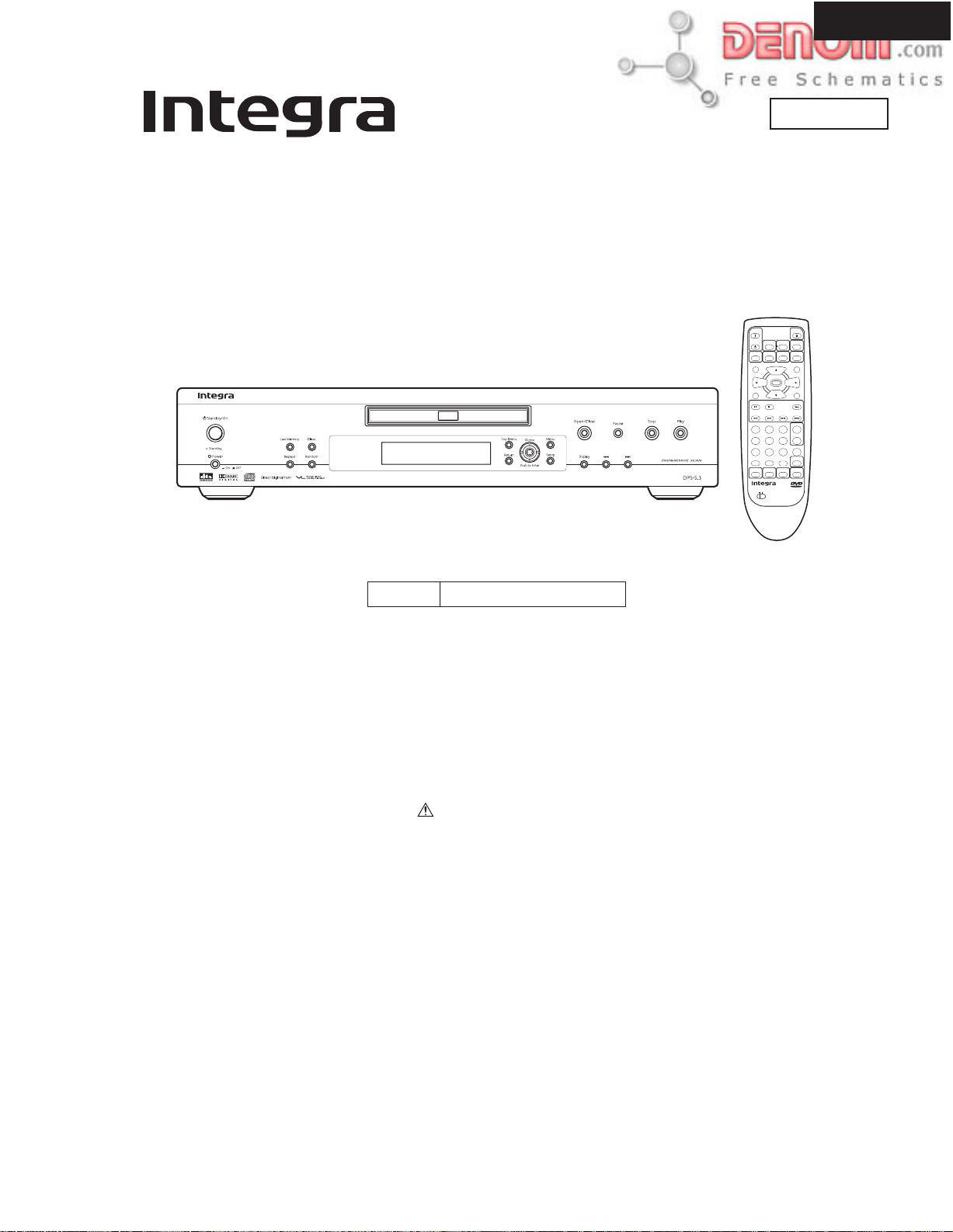
DPS-5.3
SERVICE MANUAL
Ref. No. 3726
SERVICE MANUAL
DVD PLAYER
MODEL DPS-5.3
Black model
Aug, 2002
OPEN
ON
/CLOSE
TV
ON / STANDBY
AUDIO SUBTITLE
STANDBY
ANGLE
COND. M
LAST M DIMMER DISPLAY
MENU
TOP MENU
+
-
CH
CH
+
VOL
ENTER
-
VOL
SETUPRETURN
TV/ VCR
STOPPAUSE PLAY
DOWN UPFR FF
STEP/ SLOW
+
23
1
456
-
FUNCTION M
789
SEARCH
CLEAR
+
10
0
PROGRAM
RANDOM REPEAT A-B
-
451
DV
REMOTE CONTROLLER RC
TV
DVD
RC-451DV
120V AC, 60HzBMDD
SAFETY-RELATED COMPONENT
WARNING!!
THE MARK FOUND ON SOME COMPONENT
PARTS INDICATES THE CRITICAL FOR RISK OF
FIRE AND ELECTRIC SHOCK.
WHEN REPLACING, BE SURE TO USE PARTS OF
IDENTICAL DESIGNATION.
MAKE LEAKAGE-CURRENT OR RESISTANCE
MEASUREMENTS TO DETERMINE THAT EXPOSED
PARTS ARE ACCEPTABLY INSULATED FROM THE
SUPPLY CIRCUIT BEFORE RETURNING THE
APPLIANCE TO THE CUSTOMER.
www.denom.com
Page 2
SPECIFICATIONS
DVD Player
Power supply AC 120 V, 60 Hz
Power consumption 14 W
Power consumption (standby mode) 1.4 W
Weight 3.4 kg, 7.5 lbs.
External dimensions 435 91 312 mm (W/H/D), 17-1/8" 3-9/16" 12-5/16"
Signal system Standard NTSC
Regional restriction code 1
Laser Semiconductor laser, wavelength 650 nm
Frequency range (digital audio) DVD linear sound: 48 kHz sampling 4 Hz to 22 kHz
Signal-to-noise ratio (digital audio) More than 100 dB
Audio dynamic range (digital audio) More than 96 dB
Harmonic distortion (digital audio) Less than 0.015 %
Wow and flutter Below measurable level (less than ±0.001 % (W.PEAK))
Operating conditions Temperature: 5 C to 35 C (41 F to 95 F), Operation status: Horizontal
xxx
96 kHz sampling 4 Hz to 44 kHz
Audio CD: 4 Hz to 20 kHz
x
x
DPS-5.3
Outputs
Video output 1.0 V (p-p), 75 , negative sync., pin jack 1
S-video output (Y) 1.0 V (p-p), 75 , negative sync., Mini DIN 4-pin 1
(C) 0.286 V (p-p), 75 ohm
Component video output (Y) 1.0 V (p-p), 75 , negative sync., pin jack 1
(P
B)/(PR) 0.7 V (p-p), 75
Audio output (digital output Optical) -22.5 dBm 1
Audio output (digital output Coaxial) 0.5 V (p-p), 75 , pin jack 1
Audio output (analog audio) 2.0 V (rms), 470 , pin jack (L, R) 2
Audio output (Mono) 2.0 V (rms), 470 , pin jack 1
ohm
ohm
ohm
ohm
x
ohm
ohm
ohm
x
x
x
x
x
x
www.denom.com
Page 3
SERVICE PROCEDURE-1
REPLACING THE FUSES
This symbol located near the fuse indicates that the
fuse used is show operating type, For continued protection against
fire hazard, replace with same type fuse , For fuse rating, refer to
the marking adjust to the symbol.
Ce symbole indique que le fusible utilise est e lent.
Pour une protection permanente, n'utiliser que des fusibles de meme
type. Ce demier est indique la qu le present symbol est apposre.
DPS-5.3
REF.NO.
F1
PART NO.
252252 or 1.6A-T/UL-ST2 or
252147 1.6A-TSC Fuse
DESCRIPTION
SAFETY CHECK
(Only U.S.A. model)
After correcting the original service problem perform the
following safety check before releasing the set to the customer
Connect the insulating-resistance tester between the plug of
power supply cord and terminal GND on the back panel.
Specifications: More than 10M ohm at 500V
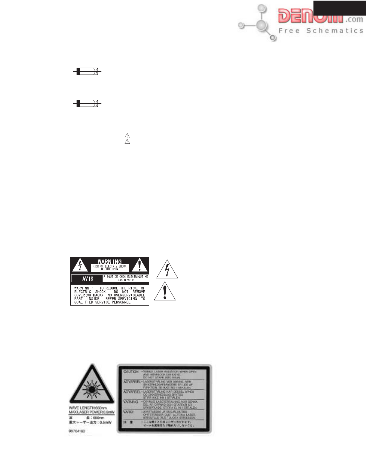
LASER WARNING LABELS
The lightning flash with arrowhead symbol, within an equilateral triangle, is
intended to alert the user to the presence of uninsulated "dangerous voltage"
within the product's enclosure that may be of sufficient magnitude to constitute
a risk of electric shock to persons.
The exclamation point within an equilateral triangle is intended to alert the user
to the presence of important operating and maintenance (servicing) instruction
in the literature accompanying the appliance.
TO REDUCE THE RISK OF FIRE OR ELECTRIC SHOCK, DO NOT EXPOSE THIS APPLIANCE TO RAIN
WARNING :
OR MOISTURE. DANGEROUS HIGH VOLTAGES ARE PRESENT INSIDE THE ENCLOSURE. DO NOT OPEN THE
CABINET. REFER SERVICING TO QUALIFIED PERSONNEL ONLY.
CAUTION :
TO PREVENT ELECTRIC SHOCK, MATCH WIDE BLADE OF PLUG TO WIDE SLOT, FULLY INSERT.
POUR EVITER LES CHOCS ELECTRIQUE, INTRODUIRE LA LAME LA PLUS LARGE DA LA FICHE DANS LA
ATTENTION :
BORNE CORRESPONDANTE DA LA PRISE ET POUSSER JUSQU' AU FOND.
www.denom.com
Page 4
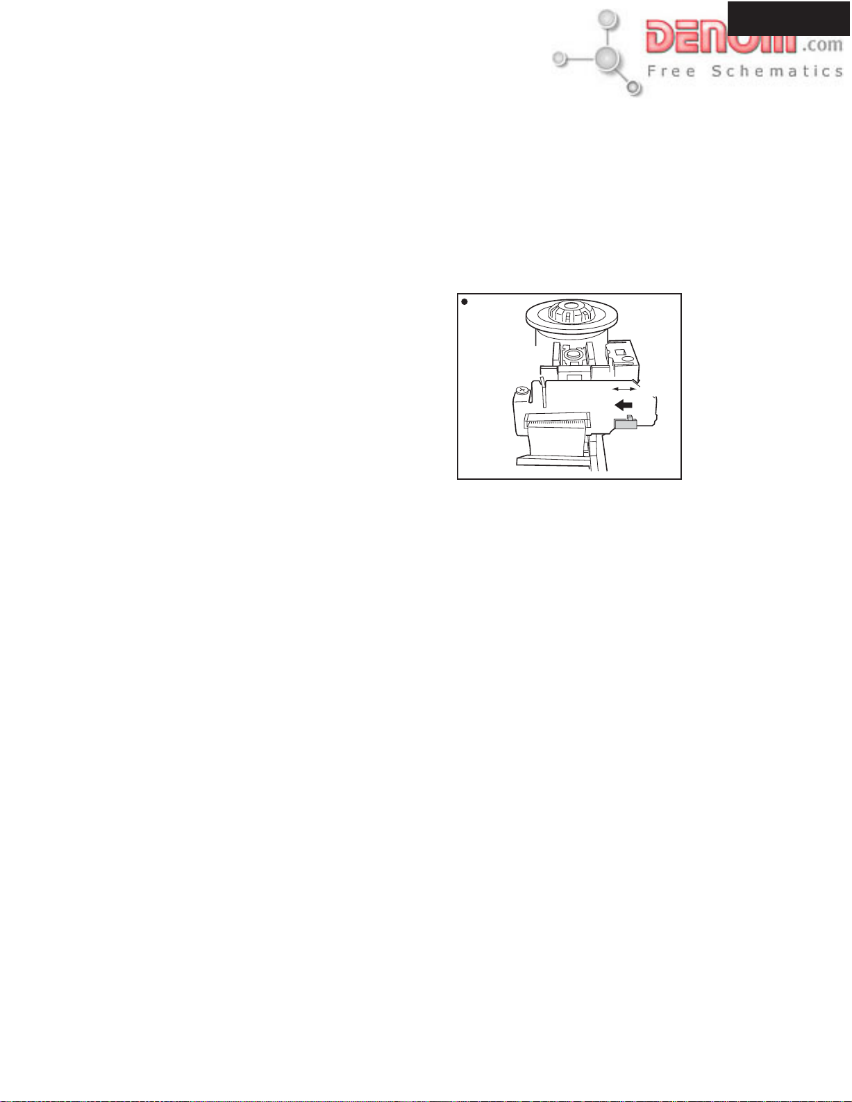
SERVICE PROCEDURE-2
1.Remove the solder of Laser Diode shorting
1-1 Connect Pickup and DVD main circuit PC board by FFC(3 pcs).
1-2 Fix it with the DVD Mecha
1-3 Remove the solder of Laser Diode shorting on Pickup.
1-4 Connect total unit of DVD Mechanism (DVD Main PCB + Mechanism) to output terminal.
PC board (NCAR7181) at CN102 and CN106
Rear View
DVDM Assy
Side
Short
DPS-5.3
Open
Short SW
2. Key check mode
Press the [STOP] and [DISPLAY] keys at the same time .
FL display light up, and check the FL display.
To cancel this process, Please press the [STOP] and [DISPLAY] keys at the same time again.
3. Factory setting (Initial setting)
3-1 Push the power switch "ON" (Mechanical switch)
3-2 Press the [STOP] and [STANDBY ON] keys at same time, and
it waits until the display of FL tube will be the display of "No Disc" from "Loading".
www.denom.com
Page 5
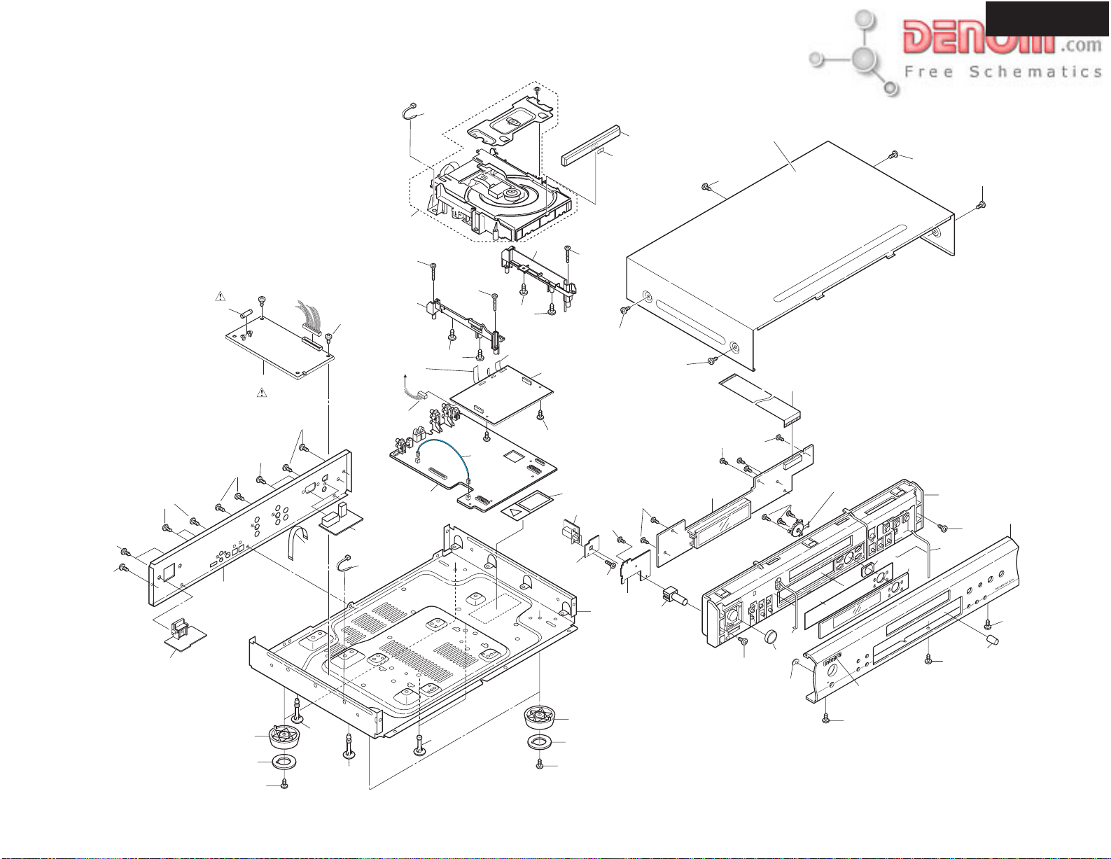
EXPLODED VIEW
03
DPS-5.3
Chassis
A63
A62
A62
U3
F1
A61
A62
U20
A62
b
A62
E751
A7
U7
E903
Z101
A13
Z102
To DVD
Mechanism
E702
E903
Z104
b
U1
A13
P351
Z103
Z104
To DVD
Mechanism
Z100
A7
a
A15
U4
A13
U6
D
V
D
A25
A1
A62
A7
A72
U5
A71
A7
A17
A62
U2
A62
a
A7
A7
A7
A73
A20
E701
A24
A21
A66
A69
S731
H
T
A
P
L
A
T
I
G
I
D
T
C
E
R
DI
A65
A67
03
A68
A62
A19
A21
A62
A7
A62
A70
A64
3
.
-5
VPS
D
A62
A3
A5
A7
A9
A9
A11
A3
A5
A7
www.denom.com
A62
Page 6
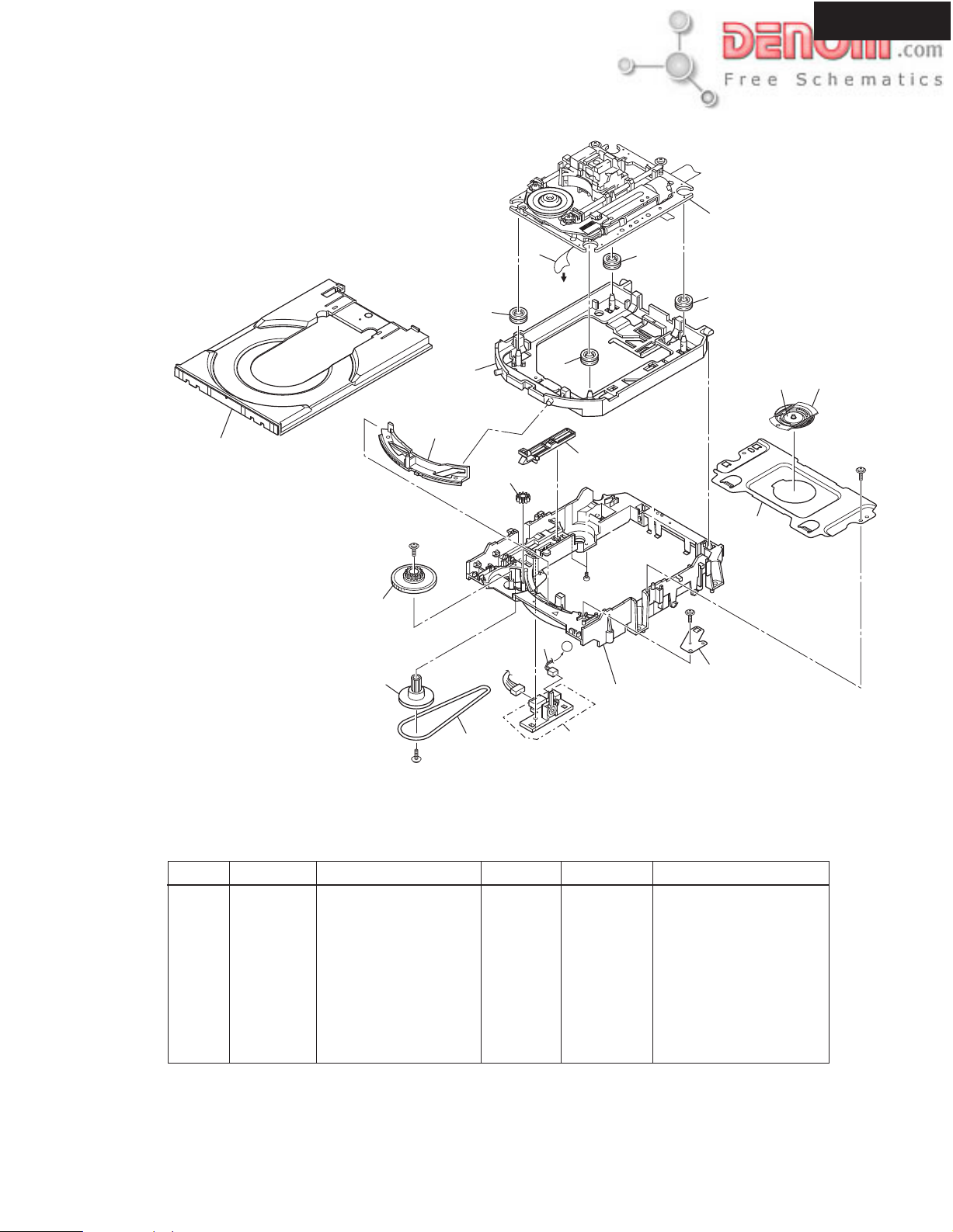
EXPLODED VIEW (LOADING MECHANISM) / PARTS LIST
EXPLODED VIEW (LOADING MECHANISM) / PARTS LIST
A
Lubricating Oil
GYA1001
GEM1036
REF.NO
PART NO.
DESCRIPTION
REF.NO.
PART NO.
DESCRIPTION
Z101 : DVD Mechanism DB-VLD301
DPS-5.3
2
23
GEM1036
15
14
Lubricating Oil
12
GYA1001
13
6
To DVDM
CN151
8
8
8
8
20
18
17
16
19
A
10
11
Lubricating Oil
GYA1001
Parts list
REF.NO
10 VNE2253
11 VNL1917
PART NO.
1 VKN1790
2 VXX2782
6 VDA1864
8 VEB1327
9 VEB1328
DESCRIPTION
Loading PC board assy
Traverse mechanism assy
FFC 26P
Rubber
Belt
Stabilizer
Loading base
9
REF.NO.
12 VNL1918
13 VNL1919
14 VNL1921
15 VNL1922
16 VNL1923
17 VNL1925
18 VNE2251
19 VNE2252
20 VNL1924
23
1
PART NO.
VNL1920
DESCRIPTION
Float base DVD
Drive cam
Gear pulley
Loading gear
Drive gear
Lever switch
Clamper plate
Bridge
Clamper
Tray
www.denom.com
Page 7
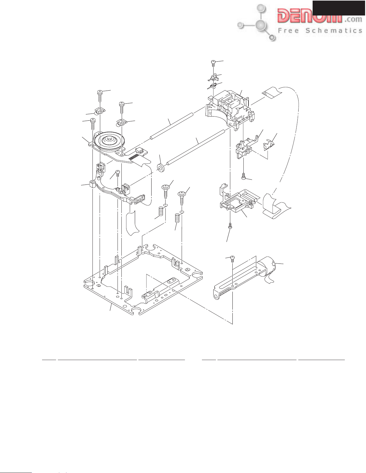
EXPLODED VIEW / PARTS LIST
TRAVERSE MECHANISM ASSY
DPS-5.3
13
18
10
1
16
18
18
10
17 (Torque : 0.12+/- 0.01 N m)
12
8
7
6
19
4 (Adjustment Screw)
4 (Adjustment Screw)
5
3
14
17
(Torque : 0.12+/- 0.01 N m)
15
.
9
.
5
11
TRAVERSE MECHANISM ASSY-S PARTS LIST
Mark No. Description Part No.
1 Spindle Motor VXM1088
2 Stepping Motor VXM1090
(CARRIAGE) (or VXM1091)
3 Pickup Assy-S OXX8003
4 Skew Screw VBA1080
5 Skew Spring VBH1335
6 Guide Bar VLL1514
7 Sub Guide Bar VLL1515
8 Hold Spring
(or VXM1089)
VNC1017
17 (Torque : 0.12+/- 0.01 N m)
16
.
2
Mark No. Description Part No.
9 Joint Spring VNC1019
NSP 11 Mechanism Chassis VNE2248
10 Support Spring VNC1020
12 Slider VNL1811
13 Spacer VNL1913
14 Joint VNL1914
15 FFC Holder VNL1915
16 Screw BBZ20P050FZK
17 Screw OBA8009
18 Screw PMA26P100FMC
NSP : Not service part
www.denom.com
19 Damper Sheet VEB1335
Page 8
BLOCK DIAGRAM
DVD Traverse
Mechanism
LOADING
MOTOR
SPDL
MOTOR
PICK UP
PU
SLIDER
SD
Clock
Generator
IC481
BA2288F
RF AMP
IC101
LA9701M
Servo
DSP
IC201
LC78652W
FTS
Driver IC
IC351
M56788AFP
SPDL
Driver IC
M56788AFP
DB-VPB306
4M
DRAM
IC712
MSM51V17805D
DVD Data
Processor
IC701
PE5108A
System
Control IC
IC601
PD6345A
16M
SDRAM
IC805
MB81F161622C
MPEG2 Decoder
(AV1) IC801
M65774BFP
8M
Flash
Memory
IC603
VYW1853
Video
Encoder
IC861
ADV7172KST
Line
Doubler
(Pro 1)
IC881
PM0026A
Progressive
conv.
120V, AC 60Hz
U3 : AC INLET PC BOARD
U20 : Power supply unit
NGPS-0020-120V
U1 : OUTPUT TERMINAL PC BOARD
PCM1742KE
Video AMP.
Driver
Q207
LA73054
D/A
Converter
Q301
NAAR-7506
Q401
Q402
Q352
V
Y
C
Y
Cb/Pb
Cr/Pr
DPS-5.3
VIDEO OUT
S-VIDEO OUT
COMPONENT
VIDEO OUT
or
PROGRESSIVE
VIDEO OUT
AUDIO OUT
OPTICAL OUT
www.denom.com
KEY
Key Controller
Q701
MPD780232QC
Q702 Display
U2 : DISPLAY CIRCUIT PC BOARD
NADIS-7606
Page 9
DPS-5.3
A
SCHEMATIC DIAGRAM-1
P701A
SCK
232SO
SI
232SCK
SO
1
2
3
4
5
232SI
XRDY
232BU
PON
232RE
XRESET
REMO
IRIN
GND2
VCOFF
GND1
EVER+5V
-27V
To Display circuit PC boardTo Main circuit PC boardTo Main circuit PC board
FLAC1
FLAC2
LT1
SRESET
CN106
GND1
1
BCK
XSI
V
G/Y
C
Y
CN102
CTS 18
LT1 19
DTR 20
RXD 22
TXD 24
SCK 27
P104
TXD 1
RXD 2
DTR 3
CTS 4
V+5D
NC 7
R102
2
R103
3
4
R104
5
R105
6
R106
7
R107
8
9
R108
10
11
12
13
R109
14
R110 47
15
16
R111
17
18
R112
19
20
R113
21
22
R114
23
24
R115
25
R116
26
R117
27
R118
28
R119
29
R120
30
3
17
R121 47
R122
R123
R124
21
R125
R126
R127
R128
R129
R130
R131
R132
R133
10K
R134
5
6
MCLK
GND2
LRCK
XCSDF
ADATA0
XSCK
ADATA1
ADATA2
6CH/X2CH
ADATA3
XMUTE
VSEL1
LFE_ON
P/XI[VSEL2]
GND3
PRG_CR
GND4
PRG_CB
GND5
PRG_Y
GND6
B/CB
R/CR
M+6V1 1
SW5V 2
M+6V2
GND1 4
GNDM1 5
GND2 6
GNDM2 7
+3.3V1 8
+12VM 9
+3.3V2 10
GND3 11
+2.5V1 12
+2.5V2 13
GND4 14
GND5 15
MICON2 16
MICON1
XRESET
S[FTOM] 23
S[MTOF] 25
AODAI 26
SQUEEZE 28
XREADY 29
LETTER 30
GNDD
BCDEFGH
U1 : OUTPUT TERMINAL PC BOARD NAAR-7605
SCK
232SO
SI
232SCK
R552
SO
0
232SI
XREADY
232BU
P_ON
232RE
R553
XRESET
0
REMO
IRIN
GND
VCOFF
GND
EVER+5V
-27V
FLAC1
FLAC2
LT1
232RESET
47
MCLK
47
BCK
47
LRCLK
47
XCSDF V
47
ADATA0 B/CB
47
XSCK C
47
XSI
R551
47
XMUTE
47
P/XI
47
PRG_CR
47
PRG_CB
47
PRG_Y
47
47
47
47
47
47
47
47
47
47
47
47
47
47
47
47
47
47
R501
0
10K
R136
R135 10K
1mm Pich FFC
For Download
R533
B/CB
V
G/Y
C
R/CR
Y
CTS
LT1
DTR
XRESET
RXD
SO_1 ADATA0 XCSDF
TXD LRCLK XSCK
SI XSI
DOUT
SCK_1
SQUEEZE
XREADY
LETTER
R137 10K
TXD
RXD
DTR
CTS
10K
R101
0
0
C101
104Z
NAAR-7605
P351A
DOUT
NC
P105
GND
SI
SO
SCK
EVER+5V
VCOFF
Q902
BA25BC0FP
VOUV
2.5
C914
100/16
104Z
C911
R904
OUT
3
Q901
025EZ5M
GND
5NC4
C903
104Z
C905
104Z
C907
104Z
2.2
C915
22/6.3
P351B
GND2VIN
ON/OFF2VIN
VOUV
OUT
3
C901
104Z
XRESET
R903
0
220/6.3
100/6.3
L351
R351
0
C351
104K
C307
470/6.3
C916
1
334Z
3.3
1
C902
220/16
C904
C906
220/16
C908
FLAC1
FLAC2
P_ON
GND
EVER+5V
-27V
To POWER SUPPLY UNIT
BK1608LM182-T
C352 104Z
C353 100/6.3
GND
M+6V
MGND
V+12V
C909
104Z
220/6.3
C910
GND
SW+5V
100K
R352
5.0
+3.3V
470K
R353
GND
GND
P902
C355
C354
020
020
14
11
12
13
VCC
Q352
TC74VHCU04T
12345
R357 470
PRG_CB
PRG_CR
PRG_Y
12.0
XMUTE
232SI
232BU
232RE
232SO
232SCK
IR
232RESET
To RC-232C PC BOARD
NAETC-7607
R505
C358
R/CR
R301
220
NC
C359
R902
10K
C364
223Z
Y11
Z1
3
Z4
Z05
EN6
VEE7
GND8
D901
0
C305
C356
020
104K
8
9
10
GND7
6
BK1608LM182-T
L353
C202
C203
C204
C303
220/6.3
C302
104Z
C301
220/6.3
C304
104Z
BCK MCLK
GND
SW+5V
C357
330
R354
180
180
R355
L352
C361
104Z
BK1608LM182-T
R206
R205
NC
0
Q202
2SA1162
NC
010
R202
R208
R207
NC
0
0
Q203
R540
2SA1162
NC
010
R203
R210
R209
NC
0
Q204
2SA1162
220
UDZS11B
1SS352
R302
1K
Q301
ZEROL 12
ZEROR 11
VCOM 10
R527
0
C920
MCLK 16
ML15
MD13
AGND 9
C205
104Z
2SC2712
NC
010
R204
R920
D920
D301
PCM1742KE
BCKIN1
DATA2
LRCKIN3MC14
GND4
VDD5
VCC6
VOUTL7
8
VOUTR
P751A
R356
C362
R539
Q920
10/16
220
100/6.3
R212
0
CR/PRG_CR
DIGITAL OUT
L355
BK1608LM182-T
C363
223Z
1
2
3
4
TC74HC4053AF
Q205
VCC16
Y15Y02
X14
X113
X012
A11
B10
C9
SW+5V
V+11V
C912
C913
47/16
UDZS5.1B
C306
104Z
220/6.3
Q303
RN1407
P/XI
104Z
GND
GND
R461
P350
V+6V
2.2K
C360
104Z
C367
NC
104Z
RI_OUT
P352
R214
CB/PRG_CB
Y/PRG_Y
R213
G/Y
C420
220/16
R480
0
C401
100/16
V+11V
100K
100K
C402
1.5K
100/16
R460 1.8K
Q460
RN1407
1.5K
R401
R457
V+6V
R456
R402
2SA1162
NC
C484
Q461
R462
3
2
1
3
2
1
681
681
Q356
P/XI
SQUEEZE
LETTER
R554
0
SQUEEZE
LETTER
Y
Y/PRG_Y
P/XI
CB/PRG_CB
CR/PRG_CR
NC
C486
C403
R403
NC
C404
C460
4.7K
OPTICAL_OUT
Q351
JFJ3000
NC
JFJ3000
3
0
R405
2
NC
10K
R407
152
C405
0
152
C406
0
R504
R404
R406
0
10K
R408
102
Q261
RN1407
C207
104K
C208
10/16
C209
R531
C210
104K
C211
10/16
C212
104K
C213
10/16
C214
104K
C215
10/16
C217
104K
C218
10/16
+B
Q401
220/6.3
NC
R483
NC
3
Q402
2
RN2403
8
+B
RN1407
Q262
R261
1.5K
C261
104Z
104K
0
150K
R215
R216
180K
0
R543
1K
R241
NJM4565M-D
NJM4565M-D
1
R411
1.5K
R409
10K
C412
220/6.3
C411
C485
C483
NJM4565M-D
8
R412
1
1.5K
R410
10K
Q263
R217
C220
R550
1
1K
100/6.3
0
R413
102
102
RN1407
Q264
RN2403
R263
1K
R262
VCC11
CV.IN2
SQUEEZE3
LETTER4
MUTE15
C.IN6 C.OUT 31
GND17
Y1.IN8
MIX.SW9
RGB.SW10
Y2.IN11
MUTE212
LPF.SW13
CB.IN14 CB.O 23
AMP2.S15
CR.IN16 CR.O 21
GND217 GND3 20
REG18
100/6.3
C219
3
8
+B
Q403
2
22K
R415
5
22K
6
NJM4565M-D
C407
R417
22K
R421
C408
R414
22K
R422
22K
0
R503
Q265
1K
R292
0
Q207
LA73054
AMP1.S 36
DRIVE1 35
DRIVE2 19
R427
10K
R423
4
-B
7
Q401
R419
22K
22K
R416
5
-B
Q402
6
NJM4565M-D
22K
R418
NJM4565M-D
Q266
R293
10K
VCC3 34
CV.O 33
GND8 32
C_DC 30
GND7 29
Y1.O 28
GND6 27
GND5 26
Y2.O
VCC2 24
GND4 22
R429 10K
NJM4565M-D
6
5
1.5K
1.5K
0
4
7
4
7
Q404
RN2403
25
470
C409
Q403
-B
R425
1.5K
R424
R420
1.5K
-B
4
R218
R219
R211
5
6
1K
1K
R220
1K
NC
R251
R542
R428
7
10K
P929A
NC
0
R201
0R534
Q251
2SC2712
R530
0
0
C415
100/16
C413
100/16
R443
270
Q405
HN1C03F
2
R445
0
R426
2.2K
2
3
R431
470
6
1
470
C410
10K
R430
Q404
+B
C419
8
GND
HN1C03F
470
R432
1
C221
470/6.3
C222
R224
C223
470/6.3
C224
470/6.3
C225
470/6.3
C226
470/6.3
R451
0
Q407
2
R452
100/16
R447
100
104K
10K
D960
2.2K
Q405
HN1C03F
R449
HN1C03F
C414
100/16
R221
75
BK1608LM182-T
R222
75
BK1608LM182-T
R223
75
R225
R226
75
0
R229
R230
100
0
BK1608LM182-T
R228
R227
100
0
R960
820
UDZS8.2B
R453
100
HN1C03F
6
R454
1
R502
0
5
2.2K
C416
102
2.2K
R446
2
Q406
R444
270
R239
R236
C960
5
2.2K
C418
102
3
4
1
6
R231
470
470
Q960
2SC2712
10/16
3
4
R441
100K
C417
R450
2.2K
HN1C03F
R448
100
R240
R237
Q407
R455
C480
102
Q406
5
0
L201
R232
0
L202
R233
0
L203
0
L204
NC
R238
0
L206
560
R235
0
L205
560
100K
472
BK1608LM182-T
R234
NC
R435
100
472
C482
100
R433
4
R442
3
100K
C481
100
472
R434
P201
G1
1
Y
3
G2
5
C
4
G3
2
SW
6
7
8
4
2
1
3
2
1
3
S-VIDEO OUT
G4
SIGNAL
P203
Y
CB
CR
P204A
1 V + 12V
2 VSEL1
3 Y
4 VSEL2
5 C
6 GNDV1
7 V
8 GNDV2
9 G
10 GNDV3
11 B
12 GNDV4
13 R
14 GNDV5
15 + 5V
16 AUDIO L
17 A GND
18 AUDIO R
19 SQUEEZE
20 V +8V
P402
L ch
R ch
COMPONENT OUT
NC
IR TERMINAL IN/OUT
MONO
3
1
L ch
2
R ch
4
AUDIO OUT
P401
www.denom.com
Page 10
A
BCDEFGH
SCHEMATIC DIAGRAM-1
P701A
SCK
232SO
SI
232SCK
SO
1
2
3
4
5
232SI
XRDY
232BU
PON
232RE
XRESET
REMO
IRIN
GND2
VCOFF
GND1
EVER+5V
-27V
To Display circuit PC boardTo Main circuit PC boardTo Main circuit PC board
FLAC1
FLAC2
LT1
SRESET
CN106
GND1
1
BCK
XSI
V
G/Y
C
Y
CN102
CTS 18
LT1 19
DTR 20
RXD 22
TXD 24
SCK 27
P104
TXD 1
RXD 2
DTR 3
CTS 4
V+5D
NC 7
R102
2
R103
3
4
R104
5
R105
6
R106
7
R107
8
9
R108
10
11
12
13
R109
14
R110 47
15
16
R111
17
18
R112
19
20
R113
21
22
R114
23
24
R115
25
R116
26
R117
27
R118
28
R119
29
R120
30
3
17
R121 47
R122
R123
R124
21
R125
R126
R127
R128
R129
R130
R131
R132
R133
10K
R134
5
6
MCLK
GND2
LRCK
XCSDF
ADATA0
XSCK
ADATA1
ADATA2
6CH/X2CH
ADATA3
XMUTE
VSEL1
LFE_ON
P/XI[VSEL2]
GND3
PRG_CR
GND4
PRG_CB
GND5
PRG_Y
GND6
B/CB
R/CR
M+6V1 1
SW5V 2
M+6V2
GND1 4
GNDM1 5
GND2 6
GNDM2 7
+3.3V1 8
+12VM 9
+3.3V2 10
GND3 11
+2.5V1 12
+2.5V2 13
GND4 14
GND5 15
MICON2 16
MICON1
XRESET
S[FTOM] 23
S[MTOF] 25
AODAI 26
SQUEEZE 28
XREADY 29
LETTER 30
GNDD
U1 : OUTPUT TERMINAL PC BOARD NAAR-7605
SCK
232SO
SI
232SCK
R552
SO
0
232SI
XREADY
232BU
P_ON
232RE
R553
XRESET
0
REMO
IRIN
GND
VCOFF
GND
EVER+5V
-27V
FLAC1
FLAC2
LT1
232RESET
47
MCLK
47
BCK
47
LRCLK
47
XCSDF V
47
ADATA0 B/CB
47
XSCK C
47
XSI
R551
47
XMUTE
47
P/XI
47
PRG_CR
47
PRG_CB
47
PRG_Y
47
47
47
47
47
47
47
47
47
47
47
47
47
47
47
47
47
47
R501
0
10K
R136
R135 10K
1mm Pich FFC
For Download
R533
B/CB
V
G/Y
C
R/CR
Y
CTS
LT1
DTR
XRESET
RXD
SO_1 ADATA0 XCSDF
TXD LRCLK XSCK
SI XSI
DOUT
SCK_1
SQUEEZE
XREADY
LETTER
R137 10K
TXD
RXD
DTR
CTS
10K
R101
0
0
C101
104Z
NAAR-7605
P351A
DOUT
NC
P105
GND
SI
SO
SCK
EVER+5V
VCOFF
Q902
BA25BC0FP
VOUV
2.5
C914
100/16
104Z
C911
R904
OUT
3
Q901
025EZ5M
GND
5NC4
C903
104Z
C905
104Z
C907
104Z
2.2
C915
22/6.3
P351B
GND2VIN
ON/OFF2VIN
VOUV
OUT
3
C901
104Z
XRESET
R903
0
220/6.3
100/6.3
L351
R351
0
C351
104K
C307
470/6.3
C916
1
334Z
3.3
1
C902
220/16
C904
C906
220/16
C908
FLAC1
FLAC2
P_ON
GND
EVER+5V
-27V
To POWER SUPPLY UNIT
BK1608LM182-T
C352 104Z
C353 100/6.3
GND
M+6V
MGND
V+12V
C909
104Z
220/6.3
C910
GND
SW+5V
100K
R352
5.0
+3.3V
470K
R353
GND
GND
P902
C355
C354
020
020
14
11
12
13
VCC
Q352
TC74VHCU04T
12345
R357 470
PRG_CB
PRG_CR
PRG_Y
12.0
XMUTE
232SI
232BU
232RE
232SO
232SCK
IR
232RESET
To RC-232C PC BOARD
NAETC-7607
220
R356
C362
100/6.3
R212
R539
0
Q920
2SC2712
10/16
R505
NC
C359
C358
R/CR
CR/PRG_CR
R902
10K
R301
220
C364
223Z
Y11
Z1
3
Z4
Z05
EN6
VEE7
GND8
D901
C356
020
104K
8
9
10
GND7
6
BK1608LM182-T
L353
C202
C203
C204
C303
220/6.3
C302
104Z
C301
220/6.3
C304
104Z
BCK MCLK
GND
SW+5V
C357
330
R354
180
180
R355
L352
C361
104Z
BK1608LM182-T
R206
R205
NC
0
Q202
2SA1162
NC
010
R202
R208
R207
NC
0
0
Q203
R540
2SA1162
NC
010
R203
R210
R209
NC
0
Q204
2SA1162
220
UDZS11B
1SS352
R302
1K
Q301
ZEROL 12
ZEROR 11
VCOM 10
R527
0
C920
MCLK 16
ML15
MD13
AGND 9
C205
104Z
NC
010
R204
R920
D920
D301
PCM1742KE
BCKIN1
DATA2
LRCKIN3MC14
GND4
VDD5
VCC6
VOUTL7
8
VOUTR
P751A
www.denom.com
Page 11
DPS-5.3
C359
10K
C364
223Z
Y11
Z1
3
Z4
Z05
EN6
VEE7
GND8
D901
0
L355
BK1608LM182-T
C363
223Z
TC74HC4053AF
Q205
SW+5V
V+11V
C912
UDZS5.1B
C306
C305
220/6.3
Q303
RN1407
1
2
3
4
VCC16
Y15Y02
X14
X113
X012
A11
B10
C9
47/16
104Z
DIGITAL OUT
P/XI
104Z
C913
GND
R461
GND
P350
RI_OUT
P352
C401
100/16
V+6V
V+11V
C402
100/16
R460 1.8K
RN1407
2.2K
C360
104Z
C367
NC
104Z
R214
CB/PRG_CB
Y/PRG_Y
R213
C420
R480
0
100K
100K
Q460
G/Y
220/16
1.5K
R401
R457
V+6V
R456
R402
1.5K
2SA1162
NC
C484
Q461
R462
3
2
1
3
2
1
Y
681
681
Q356
JFJ3000
P/XI
SQUEEZE
LETTER
R554
0
SQUEEZE
LETTER
Y/PRG_Y
P/XI
CB/PRG_CB
CR/PRG_CR
NC
C486
NC
C403
R403
NC
C404
C460
4.7K
OPTICAL_OUT
Q351
JFJ3000
NC
3
0
R405
2
10K
R407
152
C405
0
152
C406
0
R504
R404
R406
0
10K
R408
102
RN2403
Q261
RN1407
C207
104K
C208
10/16
C209
R531
C210
104K
C211
10/16
C212
104K
C213
10/16
C214
104K
C215
10/16
C217
104K
C218
10/16
NJM4565M-D
8
+B
Q401
220/6.3
NC
R483
NC
3
+B
Q402
2
Q262
R261
104K
0
150K
R215
R216
180K
0
R543
1K
R241
1
R411
1.5K
R409
10K
C412
220/6.3
C411
C485
C483
NJM4565M-D
8
1
R410
10K
Q264
RN2403
Q263
RN1407
1.5K
R262
C261
104Z
1K
R217
C220
100/6.3
100/6.3
C219
0
R550
8
+B
1
Q403
NJM4565M-D
22K
R413
5
22K
6
NJM4565M-D
102
C407
22K
102
C408
R414
R412
1.5K
R422
0
R503
Q266
Q265
RN1407
1K
R292
R293
0
R263
1K
Q207
LA73054
AMP1.S 36
VCC11
CV.IN2
DRIVE1 35
SQUEEZE3
VCC3 34
CV.O 33
LETTER4
MUTE15
GND8 32
C.IN6 C.OUT 31
C_DC 30
GND17
Y1.IN8
GND7 29
MIX.SW9
RGB.SW10
GND6 27
Y2.IN11
GND5 26
MUTE212
VCC2 24
LPF.SW13
CB.IN14 CB.O 23
AMP2.S15
GND4 22
CR.IN16 CR.O 21
GND217 GND3 20
REG18
DRIVE2 19
3
R427
2
10K
R415
R423
4
-B
7
Q401
R419
22K
R417
R421
22K
R416
5
4
-B
22K
Q402
6
NJM4565M-D
22K
22K
R418
7
NJM4565M-D
RN2403
10K
Y1.O 28
Y2.O
25
C409
R429 10K
NJM4565M-D
6
Q403
5
1.5K
1.5K
0
R425
1.5K
7
R420
4
-B
Q404
470
-B
4
R424
1.5K
R218
R219
R211
5
6
1K
1K
R220
1K
NC
R251
R542
R428
7
10K
P929A
NC
0
R201
0R534
Q251
2SC2712
R530
0
0
C415
100/16
C413
100/16
R443
270
Q405
HN1C03F
2
R445
0
R426
2.2K
2
3
R431
470
6
1
470
C410
10K
R430
Q404
R231
470
470
Q960
2SC2712
10/16
3
4
R441
100K
C417
R450
2.2K
HN1C03F
R448
100
R240
R237
Q407
R455
C480
102
Q406
5
L201
R232
L202
R233
L203
L204
NC
R238
L206
560
R235
L205
560
100K
472
0
0
0
0
0
0
BK1608LM182-T
R234
NC
R435
100
472
C482
100
R433
4
R442
3
100K
C481
100
472
R434
P201
G1
1
Y
3
G2
5
C
4
G3
2
SW
6
7
8
4
2
1
3
2
1
3
S-VIDEO OUT
G4
SIGNAL
P203
Y
CB
CR
P204A
1 V + 12V
2 VSEL1
3 Y
4 VSEL2
5 C
6 GNDV1
7 V
8 GNDV2
9 G
10 GNDV3
11 B
12 GNDV4
13 R
14 GNDV5
15 + 5V
16 AUDIO L
17 A GND
18 AUDIO R
19 SQUEEZE
20 V +8V
P402
L ch
R ch
COMPONENT OUT
NC
IR TERMINAL IN/OUT
MONO
3
1
L ch
2
R ch
4
AUDIO OUT
P401
C221
R221
104K
10K
2.2K
100
Q405
HN1C03F
R449
HN1C03F
C414
100/16
R226
0
R230
0
R228
0
R960
D960
UDZS8.2B
R453
6
R454
1
R502
0
5
2.2K
C416
102
R446
2
Q406
R444
270
75
BK1608LM182-T
R222
75
BK1608LM182-T
R223
75
R225
75
R229
100
R239
BK1608LM182-T
R227
100
R236
820
C960
100
HN1C03F
5
2.2K
C418
102
3
4
1
2.2K
6
470/6.3
C222
R224
C223
470/6.3
C224
470/6.3
C225
470/6.3
C226
470/6.3
GND
R451
0
Q407
HN1C03F
2
R452
470
R432
C419
100/16
R447
1
+B
8
www.denom.com
Page 12
DPS-5.3
A
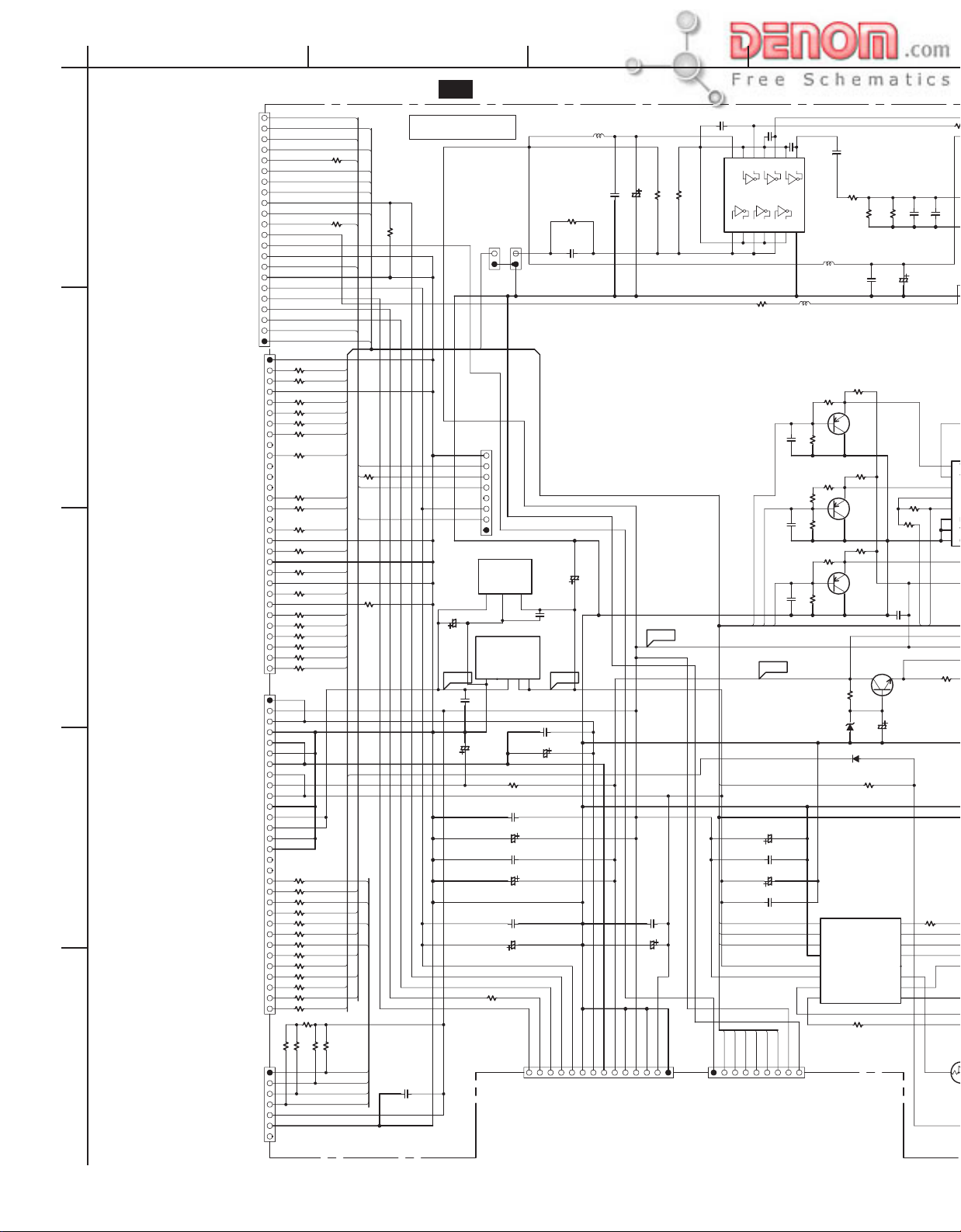
SCHEMATIC DIAGRAM-2
1
U2 : DISPLAY CIRCUIT PC BOARD
NADIS-7606
VOF_L
STB_L
2
P15 PON
P14 XRDY
3
P13 SO
P12 SI
P11 XSCK
P10
P9
P8
P7
FL_ON/OFF ENTER
39
40
192_L K2 RI
96_L INIT1
PLY_L SYSOUT
STP_L VCOFF
OPC_L IRIN
R785
41
42
43
44
45
46
47
48
49
50
51
52
53
54
55
56
57
58
59
60
192LED
96LED
PLYLED
STPLED
OPCLED
LEDO
NC5
NC6
NC7
P15
P14
P13
P12
P11
P10
P9
P8
P7
VDD2
VLOAD
VLED
P562
P661
P6P5P4P3P2
MSO_0
MSO_1
MSO_0 38
MSO_1 37
STBYLED
P364
P463
R797 10K
R790
10K
R789
10K
MSO_2
35
NC4
MSO_2 36
P166
P265
P1
232SO
232SI
SRESET
232SCK
R712
R713
R7590
R7110
0
0
NC3 34
TEST 33
R232SO 32
R232SCK 31
Q701
MPD780232GC
11G70
12G69
13G68
14G67
14G
13G
12G
11G
10G
BCDEFGH
232BU
232RE
SYSIN
SYSOUT
R788
10K
R709
R710
0
0
+5V 24
VDD0 25
SYSIN 26
R232SI 30
SYSOUT 27
R232REQ 28
R232BUSY 29
SYSRESET 12
10G71
9G72
9G8G7G6G5G4G3G2G1G
4G77
5G76
6G75
7G74
8G73
K0
K0 22
VSS0 23
VCOFF 17
RESET 6
2G79
3G78
MSO_0
K1
K1 21
K2 20
INIT1 19
GND2 18
IRIN 16
REMO 15
LT1 14
NC1 13
PON 11
XRDY 10
SO 9
SI 8
XSCK
GND1 5
X1 4
X2 3
VSS1 2
VDD1 1
1G80
U5 : STANDBY LED
PC BOARD
CN2
To P902
NADIS-7612
R747
R748
R749
R750
820
1K
S714
S715
MEMORY
R736
R735
820
1K
S704
S703
RETURN
R742
R743
820
1K
S711
R753
232SI
GND
-27V
E+5V
FLAC2
FLAC1
To NAAR-7605
Output terminal PC board
R737
1.8K
DISPLAY
R744
1.8K
VCOFF
VCOFF
GND
IRIN
IRIN
S705
RI
RI
R738
3.9K
DOWN
R745
3.9K
RESET
R755
RESET
JL771A
S706
PON
232RE
100
PON
232RE_1
UP
232BU
R756
232BU_1
R739
10K
S707
R746
10K
XRDY
100
XRDY
JL771B
OPEN
232SI
R757
232SI_1
2.7K
2.7K
R718
R717
K0K1K2
Q704
RN2403
223Z
C706
R782
Q705
REMSENS
REMO
47K
D701
1SS352
P710A
Q703
BMR-0101D
O
G
C704
100/6.3
R716 220KR715
UDZS5.6B
R714
4.7K
I
D702
C703
22/50
K0
STB_L
VOF_L
K1
K2
Destination
1K
R727R726
0
R724 R725
MSO_1
7
C702
104Z
0
MSO_2
NC
R799
R708
R798
R707
R706
R705
R704
R703
R702 0
C701
56K
R723
10K
R722
INIT1
0
0
0
0
0
0
0
100/6.3
REMO
LT1
RESET
R701
R721R720
1M
R786 R787
SYSIN
2.7K
R719
X701
5.00MHZ
10K
390
S712
CLEAR
R733
390
S701
T.MENU
R740
390
S709
PAUSE
R751
232RE
RANDOM
MENU
STOP
R752
232BU
470
S713
R734
470
S702
R741
470
S710
LT1
LT1
SRESET
REPEAT
SETUP
PLAY
100
R754
SO
100
SO
S708
DOWN
UP
RIGHT
LEFT
SI
232SCK
R758
SI_1
232SCK
R771
1.8K
V_OFF
P731
XSCK
232SO
100
XSCK
232SO
S721
DIMMER
7
6
5
4
3
2
1
P701
R772
3.9K
S722
STANDBY
Q721
RN1407
ENTER
S731
NPS-115-S673
R773
S723
D721
STANDBY
NAPS-7609
U3 : INLET TERMINAL
PC BOARD
U20 : POWER SUPPLY UNIT
24150020A NGPS-0020
P982A (BROWN) P982B (WHITE)
P981B
P981
To Output terminal PC board
CN1
P982B (BROWN)P982A (BROWN)
C991
S991
NASW-7613
U6 : POWER SWITCH
PC BOARD
Q706
BD4742G
2S
FL_ON/OFF
Q723
4
R781
R552
2S
0
Q724
R780
P15
P14
F1 48
P14 43
P15 44
P13
P12
P11
P10
P10 39
P11 40
P12 41
P13 42
P9P8P7P6P5P4P3P2P1
38
P7 36
P8 37
P9
P2 31
P3 32
P4 33
P5 34
P6 35
13G
12G
12G16
13G17
9G8G7G6G5G4G3G
11G
10G
8G 12
9G 13
10G14
11G15
7G 11
14G
P1 30
14G18
Q702FL-545
2G
1G
1G 5
2G 6
3G 7
4G 8
5G 9
6G 10
NC
24531
F2' 1
NOTE
.
THECOMPONENTS
REPLACE ONLY
.
VOLTAGE (MEASUREDWITH VOLTMETER) IS
.
ELECTROLYTIC CAPACITORS ()ARE IN F/WV.
.
ALL CAPACITORS ARE IN pF/50WV UNLESS OTHERWISE NOTED.
EX) 030- 3pF 330- 33pF 331- 330pF 333- 0.033uF
.
ALL RESISTORS ARE IN OHMS 1/6WATTS UNLESS OTHERWISE NOTED.
.
THE THICK LINES ON PC BOARD ARE THEPRINTING SIDE OF THE PARTS.
EX) PRINTING SIDE
.
CIRCUIT IS SUBJECT TO CHANGE FOR IMPROVEMENT.
IDENTIFIED
WITH PART
BY MARK
NUMBER SPECIFIED.
ARE CRITICAL FOR
SAFETY
DC VOLTAGE.(NO INPUT SIGNAL)
u
CAUTION
FOR CONTINUED PROTECTION
AGAINST FIRE HAZARD, REPLACE
ONLY WITH FUSE OF SAME TYPE
VA
AND RATING INDICATED.
ATTENTION
AFIN D'ASSURER UNE PROTECTION
PERMANENTE CONTRE LES RISQUES
D'INCENDIE, REMPLACER UNIQUEMENT
VA
PAR UN FUSIBLE DE MEME TYPE
ET CALIBRATION COMME INDIQUE.
THIS SYMBOL LOCATED NEAR THE FUSE INDICATES
THAT THE FUSE USED IS SLOW OPERATING TYPE
FOR CONTINUED PROTECTION AGAINST FIRE
HAZARD,REPLACE WITH SAME TYPE FUSE. FOR FUSE
RATING REFER TO THE MARKING ADJACENT TO THE SYMBOL.
CE SYMBOLE INDIQUE QUE LE FUSIBLE UTLISE EST
E LENT.POUR UNE PROTECTION PERMANENTE,N'UTILISER
QUE DES FUSIBLES DE MEME TYPE. CE DARNIER EST
INDIQUE LA QU LE PRESENT SYMBOL EST APPOSE.
5
www.denom.com
Page 13
DPS-5.3
A
SCHEMATIC DIAGRAM-3
U8 : RC-232C CONNECTION PC BOARD
1
BK1608L
M182-T
C814
L801
D801
1SS355
2
100/6.3
BCD
NAETC-7607
To OUTPUT TERMINAL PC BOARD
REQ
BUSY
C810
R808
1
2
PORT16
SDATAIN
X801
5.00MHZ
7X16X25
VSS
RESET
47
4
RESET
R807
3
IC
SCK
SDATAOUT
100/6.3
C811
104Z
EVER+5V
P751B
RI
RESET
GND
15
RXD
P802
R801
1M
REQ
SCK
BUSY
SDATAIN
SDATAOUT
0
0
0
0
R805
R804
R803
R802
14
13
REQ
BUSY
12
NC
9
11SI10
SO
SCK
Q802 MPD789071MC
0
R806
8
VDD
PORT117
PORT218
TXD16
PORT319
PORT420
PORT521
PORT622
PORT723
PORT824
PORT925
PORT1026
PORT1127
PORT1228
PORT1329
PORT1430 PORT15
3
1/50
C802
C803
1/50
C812
L801
BK1608LM182-T
C813
104Z
100/6.3
RXD_FL
TXD_FL
RTS_FL
47
R812
47
R809
R823
47
CTS_FL
9
1011
Q803 MPD4721GS
12131415161718
1/50
C801
1
2
3
4
5
6
7
8
19
20
1/50
C804
47
R810
R811
10K
3.3K
R820
C815
223
4
RN1402
UMG9N
Q804
Q806
R821
Q805
10K
R822
RN1402
Q806
UMG9N
ON3131
Q801
100
5
P803
BK1608LM182-T
L802
RS-232C CONNECTOR (9PIN D-SUB CONNECTOR)
BK1608LM182-T
BK1608LM182-T
L803
L804
P801
BK1608LM182-T
L805
www.denom.com
Page 14
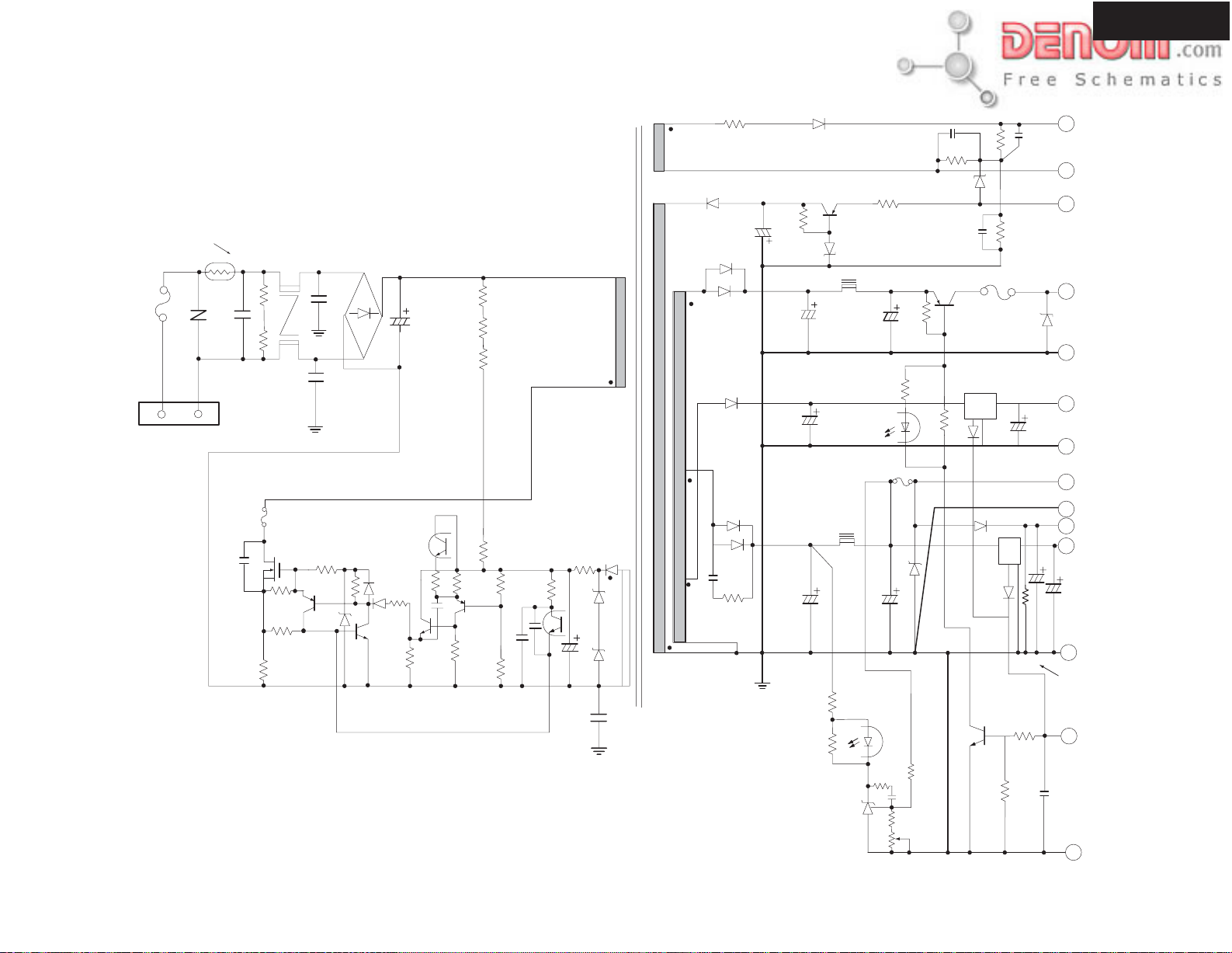
DPS-5.3
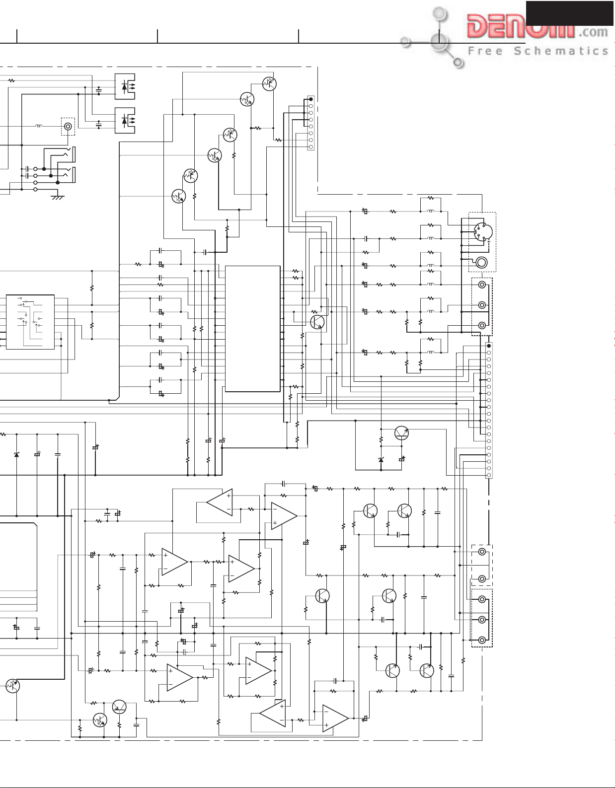
SCHEMATIC DIAGRAM
Power supply unit
24150020A NGPS-0020
Except <MDD>
C1
R1
L1
C18
TH1
F1
VS1
R2
CN1
AC-H AC-G
TF1
R35
R10
Q1
R9
Q3
D24
C2
R17
C17
D1-D4
R33
T
1
7
6
C6
R3
R4
R5
PHC2-1
R18
D6
Q5
R40
D5
C10
R13
R14
Q7
R22
R15
Q8
R32
R34
C16
C32
C11
PHC1-1
4
5
2
D12
D9
1
C9
8
9
10
D13
16
13 14 15
R37
C3
D26
D14
D15
11 12
D11
D15
C25
R30
R36
C21
D7
R2
R24
D8
L4
L6
R25
IC2
C15
PHC2-2
CP1
C21
R19
PHC
1-2
C23
D17
Q4
C5
C7
3
R28
C27
R20
D19
C31
Q2
R6
R11
R27
VR1
R41
CP2
IC3
D21
D23
IC4
D25
Q6
R7
R26
D18
R38
R12
C26
C12
3
2
1
9
10
13
C19
14
7
8
5
11
C8
12
100 ohm 1W
<MDD,MJJ> only
4
C29
6
AC4.5V
47ohm
-27V
5-15mA
SW+15V
50-400mA
GND
SW+3.3V
400-900mA
GND
+6V
20-1200mA
MGND
E+5V
10-100mA
SW+5V
200-600mA
GND
Pcont
GND
www.denom.com
Page 15
1
234567
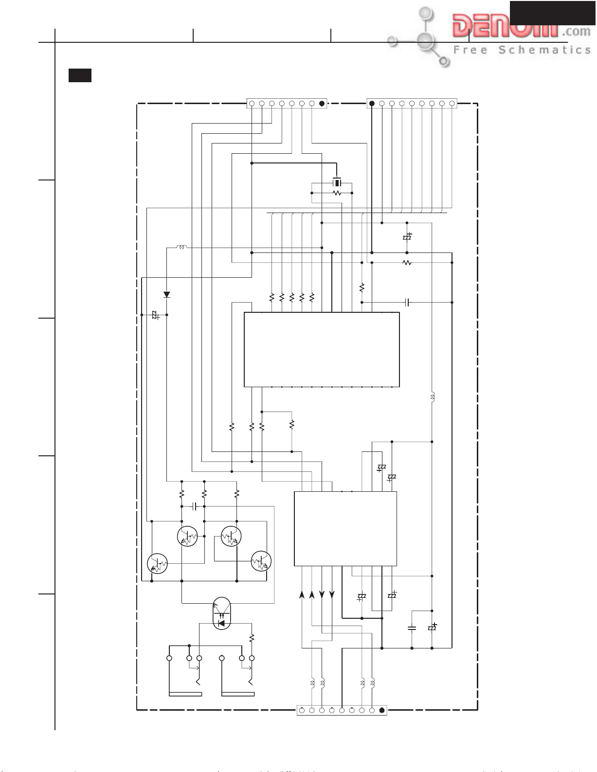
SCHEMATIC DIAGRAM (Page 1)
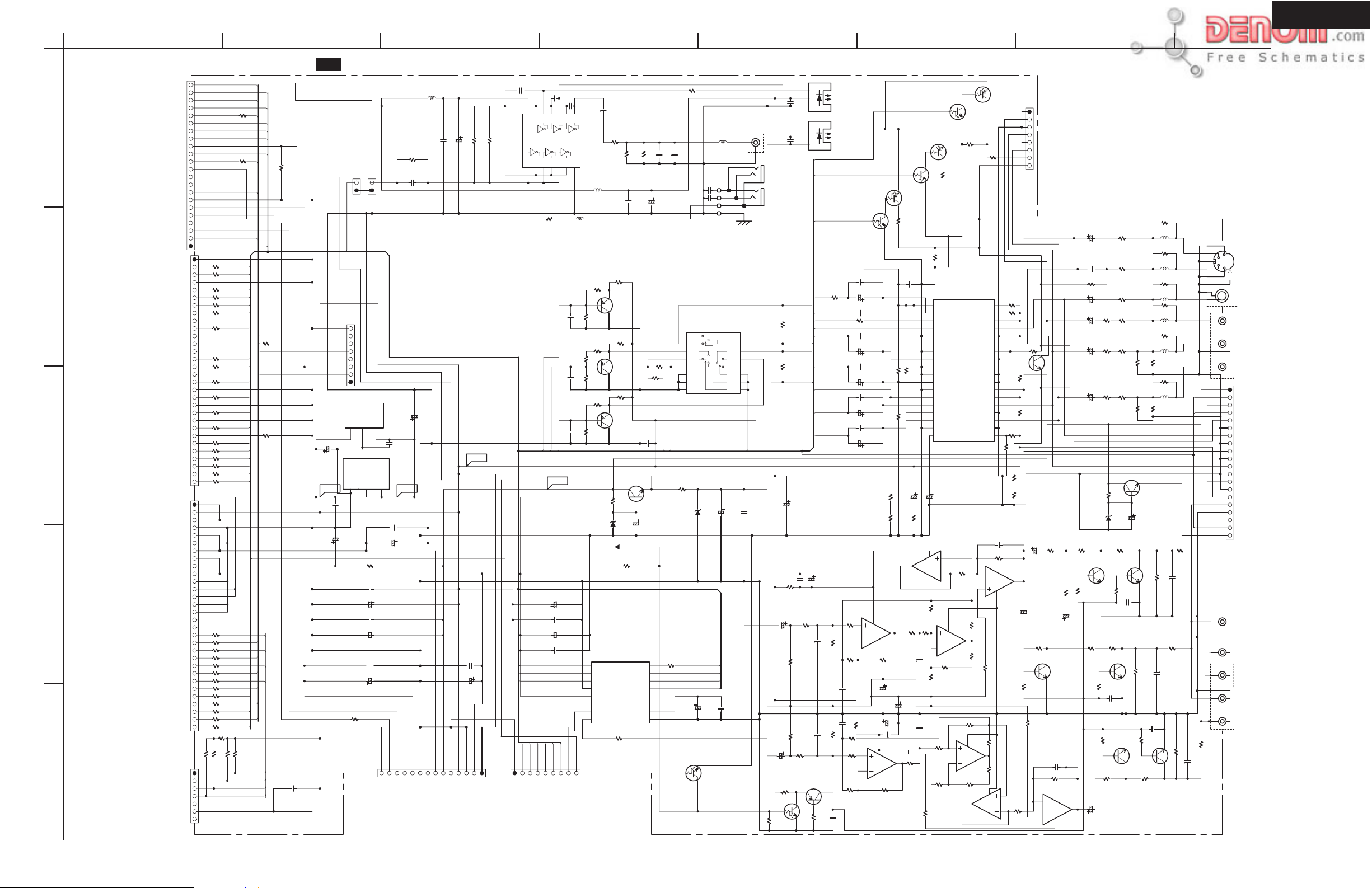
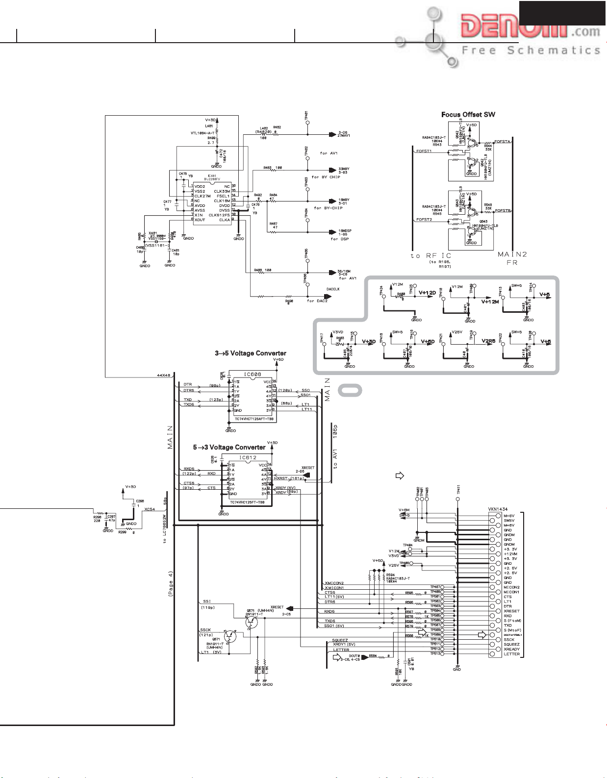
Z100 :Main circuit PC board (DB-VPB306)
A
B
Page 2
Page 2
3
Page 2
(V) (V)
1
(RF)
(RF)
Page 2
(F)
(T)
(T)
(V)
(V)
(A)
(F)
(A)
(F)
(T)
(A)
(F)
2
(T)
C
D
CN120
To Pick up assy
CN601
CN151
Load PCB
For Mecha
connector
(RF)
(F)
(F)
(T)
(F)
(F)
(T)
Page 2
(F)
(T)
(T)
(F)
(F)
(F)
(S)
CN251
To Stepping motor
(S)
(Carriage)
CN3
(T)
(T)
(F)
(F)
(T)
(T)
(F)
(F)
(T)
(T)
To Spindle motor
www.denom.com
Page 16
1
234567
SCHEMATIC DIAGRAM (Page 2)
Z100 :Main circuit PC board (DB-VPB306)
A
VYW1958-A
B
C
Page 3
Page 1
Page 1
R607
47k
6.8k
Page 1
Page 1
Page3
Page3
Page3
page 4
To CN15
D
CN512
MECHA
Page1
To CN15
Page 4
Video encoder
IC861 45p
page 4
www.denom.com
TP
page 1 IC201
Page 17
CLOCK GENERATOR
DPS-5.3
8
Page 3Page 1
Page 1
Page 3
DSP
Page 1
R489
220
Page 4
9
220/4
: The power supply is shown with
the marked box.
Page 3
(D)
(D)
: AUDIO (DIGITAL) SIGNAL ROUTE
(D)
(D)
CN401
2
4
6
8
10
12
14
16
18
20
22
24
26
28
30
1
3
5
7
9
11
13
15
17
19
21
23
25
27
29
CN102
To Output circuit PC board
www.denom.com
Page 18

1
234567
SCHEMATIC DIAGRAM (Page 3)
Z100 :Main circuit PC board (DB-VPB306)
A
B
C
(VD)
***
C742
C705
***
(VD)
(V)
220/4
IC712
4M MSM51V17805D-60TS
To SCRUT 7,21, 68, 188P
to CN15
page 4
Page 1 IC201
Page 1
R334
to CN401
D
Page 2/ IC601
Page 2/ IC601
Page 2/ IC601
Page 3 IC 801
Page 1 IC 201
(AD)
(AD)
www.denom.com
Page 2 IC 601
(V)(V)
Page 1
to Page 1
Page 19

from AVFrom AV1 88 pin IC801
(VD)
(V)
: RF (VIDEO) SIGNAL ROUTE
(VD)
: VIDEO DATA SIGNAL ROUTE
(AD)
: AUDIO DATASIGNAL ROUTE
: AUDIO SIGNAL ROUTE
(D)
: AUDIO (DIGITAL) SIGNAL ROUTE
Page 2
DPS-5.3
8
(VD) (VD)
(D)
IC801
(VD)
(D)
from Clock generator Page 2
from Clock generator Page 2
MAIN/ADDRESS/DATA from FR30 Page 2 IC601
from SCRUT Page 3 IC701
Page 2 IC601
www.denom.com
Page 20

1
234567
SCHEMATIC DIAGRAM (Page 4)
Z100 :Main circuit PC board (DB-VPB306)
Page 2
A
B
Page 3
Page 2
(VD) (VD)
Page 3
(Cr)
(Cr)(Cr)
(Cb)
(Cb)
(Cb)
(Y)(Y)
(Y)
(V) (V) (V)
C
D
(VD) (VD)
Page 2
(Y)
(Y)
Page 2
(C) (C)
(V)
(Y)
(V)
(Y)
(C)
(C)
(Y) (Y)
(Cr)
(Cb)
(Cr)
(Cb) (Cb)
www.denom.com
Page 21

(Cr)
(Cb)
(Cr)
8
(VD)
: VIDEO DATASIGNAL ROUTE
(V)
: V SIGNAL ROUTE
(Y)
: Y SIGNAL ROUTE
(C)
: C SIGNAL ROUTE
(Y)
: Y SIGNAL ROUTE
(Cb)
: Cb SIGNAL ROUTE
(Cr)
: Cr SIGNAL ROUTE
: AUDIO SIGNAL ROUTE
DPS-5.3
(Cb)
(Y)(Y)
(V)
(Y) (Y)
(C)
(Cr)
(Cr)
(Cr)
Page 3
(Y)
(Cb)
(Cr)
Page 2
Page 3
Page 3
(V)
(Y)
(Cr)
(C)
(Y)
(V)
(Cb)
(Y)
(Cb)
(Cr)
(Y)
(Cr)
(Y)
(Cb)
(Y)
(C)
(V)
(Y)
(Cb)
(Cr)
(Cb)
To Output terminal PC board
(Y)
(Y)
Page 2
CN106
www.denom.com
Page 22

DPS-5.3
10
1
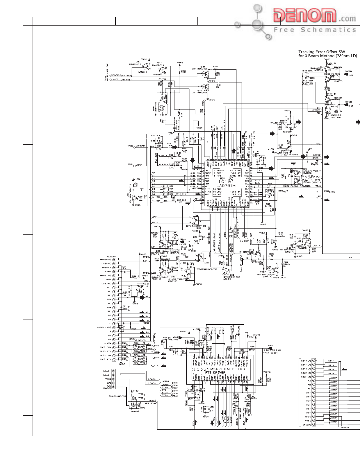
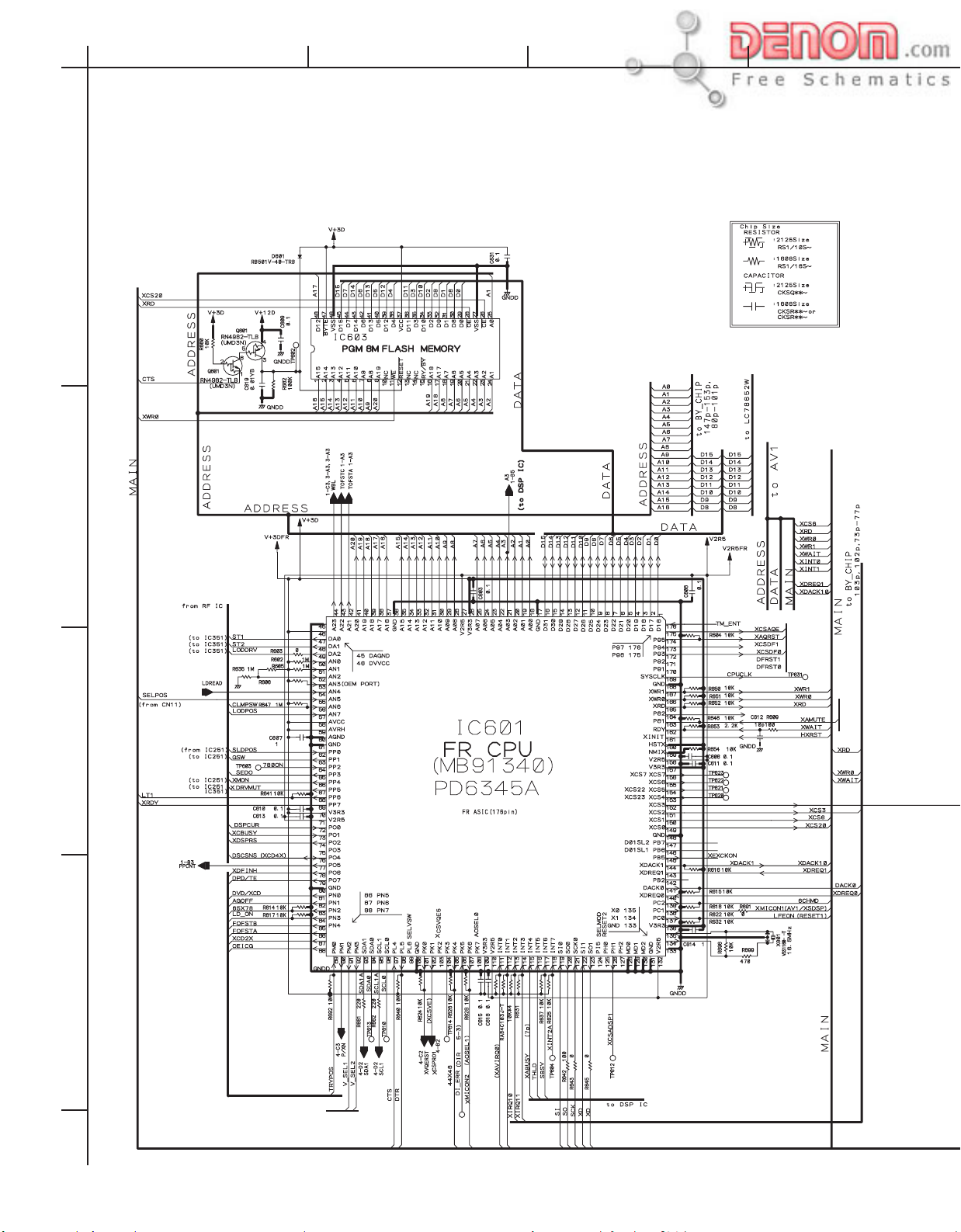
SCHEMATIC DIAGRAM (Page 1)
Z100 :Main circuit PC board (DB-VPB306)
Page 2
A
B
234567
(RF)
: RF SIGNAL ROUTE
(V)
: RF (VIDEO) SIGNAL ROUTE
(A)
: RF (AUDIO) SIGNAL ROUTE
(AD)
: AUDIO DATA SIGNAL ROUTE
(F)
: FOCUS SERVO LOOP LINE
(T)
: TRACKING SERVO LOOP LINE
(S)
: SLIDER SERVO LOOP LINE
V+5V
3V to 5Volt
Q171
RN4982-TLB
(UMD3N)
5
DF OUT
From DSP IC
54p
6
2
1
4
3
15p
82k
10k
22k
Page 3
IC701 DVD Decoder
Page 2
0.01
TC7SZU04F
IC304
470
100k
1k
3.3k
(V) (V)
Page 2
3
Page 2
(V) (V)
1
(RF)
(RF)
Page 2
(F)
(T)
(T)
(V)
(V)
(A)
(F)
(A)
(F)
(T)
(A)
(F)
2
(T)
Page 3
(V)
Page 1
to RF IC (IC 101)
28p
8
C
D
CN120
To Pick up assy
CN601
CN151
Load PCB
For Mecha
connector
(RF)
(F)
(F)
(T)
(F)
(F)
Page 2
(AD)
Page 3
BY CHIP
(T)
(F)
5
(A)
(F)
(T)
7
Page 2
FR CHIP (IC601)
Page 3
BY CHIP (IC701)
162p
(T)
(F)
(A)
(F)
(T)
Page 2
FR CPU
(T)
Page 2
(F)
(T)
(T)
(F)
(F)
(F)
(S)
CN251
To Stepping motor
(S)
(Carriage)
CN3
(T)
(T)
(F)
(F)
(T)
(T)
(F)
(F)
(T)
(T)
To Spindle motor
To Q171
From FR CPU
Page 2/3
9
8
Page 3
Page 3
111110
www.denom.com
Page 23

DPS-5.3
1
234567
SCHEMATIC DIAGRAM (Page 2)
Z100 :Main circuit PC board (DB-VPB306)
A
VYW1958-A
Page 1
B
Page 1
Page 3
Page 1
Page3
Page3
CLOCK GENERATOR
R489
8
Page 3Page 1
Page 1
Page 3
220
Page 4
C
D
CN512
MECHA
Page1
9
Page3
220/4
Page 1
: The power supply is shown with
the marked box.
R607
47k
6.8k
TP
page 4
To CN15
DSP
Page 1
Page 3
(D)
: AUDIO (DIGITAL) SIGNAL ROUTE
CN401
1
2
3
4
5
6
7
8
9
10
11
12
13
14
15
16
17
18
19
20
21
22
23
24
(D)
25
(D)
26
27
28
29
30
(D)
CN102
To Output circuit PC board
To CN15
Page 4
Video encoder
IC861 45p
page 4
page 1 IC201
www.denom.com
Page 24

DPS-5.3
1
234567
SCHEMATIC DIAGRAM (Page 3)
Z100 :Main circuit PC board (DB-VPB306)
A
***
C742
C705
B
8
(V)
: RF (VIDEO) SIGNAL ROUTE
(VD)
: VIDEO DATA SIGNAL ROUTE
(AD)
: AUDIO DATASIGNAL ROUTE
To SCRUT 7,21, 68, 188P
220/4
IC712
4M MSM51V17805D-60TS
***
to CN15
page 4
from AVFrom AV1 88 pin IC801
(VD)
: AUDIO SIGNAL ROUTE
(D)
: AUDIO (DIGITAL) SIGNAL ROUTE
Page 2
C
D
(VD)
Page 2/ IC601
Page 2/ IC601
Page 2/ IC601
(VD)
(AD)
to CN401
(V)
(VD) (VD)
Page 1 IC201
Page 1
R334
(V)(V)
Page 1
to Page 1
(D)
(D)
from Clock generator Page 2
from Clock generator Page 2
IC801
(VD)
Page 3 IC 801
Page 1 IC 201
(AD)
from SCRUT Page 3 IC701
Page 2 IC 601
Page 2 IC601
MAIN/ADDRESS/DATA from FR30 Page 2 IC601
www.denom.com
Page 25

DPS-5.3
1
234567
SCHEMATIC DIAGRAM (Page 4)
Z100 :Main circuit PC board (DB-VPB306)
Page 2
A
Page 3
Page 2
(VD) (VD)
B
(Cr)
8
(VD)
: VIDEO DATASIGNAL ROUTE
(V)
: V SIGNAL ROUTE
(Y)
: Y SIGNAL ROUTE
(C)
: C SIGNAL ROUTE
(Y)
: Y SIGNAL ROUTE
(Cb)
: Cb SIGNAL ROUTE
(Cr)
: Cr SIGNAL ROUTE
: AUDIO SIGNAL ROUTE
(Cr)(Cr)
(Cr)
(Cb)
(Cb)
(Cb)
(Y)(Y)
(Y)
(Cb)
(Cr)
(Cb)
(Y)(Y)
C
D
Page 3
(VD) (VD)
Page 3
(Y)
(Cb)
(V) (V) (V)
(V)
(Cr)
Page 2
Page 3
Page 3
(Cr)
(Cr)
(V)
(Y)
(Cr)
(C)
(Y)
(V)
(Cb)
(Y)
(Cb)
(Cr)
(Y)
(Cb)
(Cr)
(Cb)
(Y)
(C)
(Y)
(V)
(Y)
(Cb)
(Cr)
To Output terminal PC board
Page 2
CN106
(Y)
(Y)
(Y) (Y)
Page 2
(V)
(Y)
(C)
(C) (C)
(V)
(Y)
(C)
(Y) (Y)
(Cr)
(Cr)
(C)
(Cr)
(Y)
(Y)
Page 2
(Cb)
(Cb) (Cb)
www.denom.com
Page 26

PC BO ARD CONNECTION DIAGRAM
U3 :
Inlet terminal PC board
NAPS-7609
P981B
H
P981B
L
25137609
NCPS-7609
P982A
BROWN
BRN
BRN
WHT
CN1
U20 :
NGPS-0020A
Power supply unit
P982B
WHITE
Z100 : Main circuit PC board
IC701
CN52
IC712
CN401
To CN102
IC601
DB-VPB306
Pickup
CN120
IC805
IC201
IC801
DPS-5.3
U1 : NAAR-7605
Output terminal PC board
P104
NC
TXD
CTS
DTR
RXD
V+5D
CN251CN3
GNDD
P351A
GND
P902
+3.3V
IC351
CN15
To CN106
DOUT
P351A
GND
SW+5V
GND
V+12V
MGND
M+5V
GND
EVER+5V
P ON
FLAC2
FLAC1
-27V
GND
AUDIO L
AUDIO R
SQUEEZE
P250A
V+12V
VSEL1
C
VSEL2
Y
GNDV1
V
GNDV2
G
GNDV3
B
GNDV4
R
GNDV5
+5V
GNDA
V+8V
P751A
P292A
U7 : NAETC-7607
RS-232C treminal
PC board
P751B
P801
9 Pin D sub Connector
GND
+3.3V
GND
CN2
SW+5V
GND
V+12V
MGND
M+5V
GND
EVER+5V
P ON
FLAC2
FLAC1
-27V
U6 : NASW-7613
Power switch
PC board
P982CP982D
DVD mechanism
CN601
U5 : NADIS-7612
Standby LED
PC board
Standby
JL771B
JL771A
www.denom.com
CN102
U2 : NADIS-7606
Display circuit PC board
CN106
P701A
P711
Cursor button
(Jog dial)
RESET
GND
P710
P731
-
Left
GND
Right
EnterUpDown
7
22
SRESET
NC
P701B
SI
RI
SO
LT1
-27V
E+5V
GND1
GND2
FLAC2
FLAC1
VCOFF
SCK
PON
232SI
XRDY
232BU
232RE
232SO
RESET
232SCK
Page 27

DPS-5.3
A
PRINTED CIRCUIT BOARD VIEW-5
Z100 : MAIN CIRCUIT PC BOARD DB-VPB306
1
2
BCD
3
4
5
SIDE A
www.denom.com
Page 28

DPS-5.3
A
PRINTED CIRCUIT BOARD VIEW-5
Z100 : MAIN CIRCUIT PC BOARD DB-VPB306
1
2
BCD
3
4
5
SIDE B
www.denom.com
Page 29

DPS-5.3
A
BCD
PRINTED CIRCUIT BOARD VIEW FROM SOLDERING SIDE-1/2
1
U1 : OUTPUT TERMINAL PC BOARD (NAAR-7605)
C906
C911
C920
12
AUDIO_11V
7
J303
15
J302
15
J299
J337
J298
P902
J295
12
C902
7
C912
C420
J294
20
AUDIO_6V
J291
J292
C403
J286
C405
7
J290
C406
C408
12
C226
J287
7
J288
7
J289
J284
J285
17
J282
C208
C213
C211
12
J281
C407
7
J283
C908
J293
J280
C404
J271
J267
C401
C402
25
17
J278
15
J277
7
C215
J279
NCAR-7605
25137605B
C303
J273
J276
J274
7
17
20
7
AUDIO_6V
AUDIO_11V
C305
J275
7
J272
C960
J269 J258
15
J270
7
J268
J259
C220
J253
C219
C218
2
17
17
J260
15
J265
J264
J263
C301
J261
15
J251
J250
25
J249
J257
7
J247
J246
7
J245
J254
J255
J256
7
J252
15
12
22
22
17
17
15
17
17
17
7
J230
20
J248
J231
7
7
J229
J243
7
J227
J244
J242
20
J266
15
J262
25
15
J332
P402
P350
P352
P751A
J330
J335
P201
J334
+12V
VSEL1CVSEL2
J333
P401
Y
P203
C223
15
C362
20
J331
J329
J328
J324
7
17
VGB
GND
P292A
J336
20
C353
J314
GND
P351B
J323
17
J316
GND
J313
J315
C415
MUTE
GND
J311
J312
J322
12
+5V
J309
J310
C910
C904
7
J325
A_GND
J308
7
J320
12
C414
AGND
AU_L
J306
3.3V
J307
C413
SQUE
AU_R
J340
SW_5V
J305
J304
C486
C411
C419
C412
C485
P204A
7
+8V
J317
J297
J301
C221
J296
J338
C225
7
7
J300
J327
7
J339
J326
J321
J318
15
J319
R
GND
15
C224
7
15
15
P104
2
P352
Q351
P350
Q356
Q351
Q356
3
P401
7
P402
P203
4
P201
J223
J208
C915
CN102
CN102
J222
J221
7
J202
7
J203
CN106
CN106
7
12
12
12
12
J204
J205
J206
J207
7
P701A
J201
P105
P710A
P351A
J240
J241
J239
J233
J234
J235
J238
J236
J237
20
J218
27
J219
J232
27
J220
22
J216
27
J217
27
J214
27
J215
27
J213
27
J212
27
J209
27
J210
30
J211
20
J228
25
17
J224
J225
J226
Component side
5
www.denom.com
Page 30

DPS-5.3
A
PRINTED CIRCUIT BOARD VIEW-5
Z100 : MAIN CIRCUIT PC BOARD DB-VPB306
1
2
BCD
3
4
5
SIDE B
www.denom.com
Page 31

DPS-5.3
A
BCDEFGH
PRINTED CIRCUIT BOARD VIEW FROM SOLDERING SIDE-2
1
2
U2 : DISPLAY CIRCUIT PC BOARD (NADIS-7606)
P731
27
J704
17
J702
J703
15
20
J705
STOPPLAY
7
P701B
J701
S710S711
PAUSE
S709
J706
C703
RWFF
27
OPEN
D703D704D705
S708
DISPLAY
S705S706S707
J707
J710
J709
J708
J712
MENU
S703
S704
SETUP
P710A
Q703B
7
J713
J714
D707
D706
20
J748
7
Q724
Q723
12
25
J742
J745
J741
J743
Q705
Q705
J744
J725
TOP-MENU
12
J735
7
S701
J723
J722
15
15
S702
RETURN
C701
J727
15
J726
J728
J731
J730
J729
7
17
25
X701
J733
J734
J732
R5761
30
30
20
J737
J736
J739
R785
J740
7
J738
7
J711
12
J718
22
J720
J721
7
7
7
J715
J719
J716
J717
J724
7
J746
J749
J747
J750
C704
NCDIS-7606
JL771A
J751
CLEAR
S712
S713 S714
2
25137606
LAST_MEMORY
S715
REPEATRANDOM
R5761
Component side view
3
R576
R745
R797
R739
R746
R732
Q780
R736
R731
R730
R742
Q708
4
Q707
R741
R740
R738
R737
R744
R735
R743
Q706
R714
R753
R757
R579
R752
R578
R756
R755
R751
R709
R733
R718
R734
R786
R720
R754
R787
R721
R717
R577
R758
R507
R708
R799
R798
R707
R706
R705
R704
R703
R702
R575
R574
R701
R573
R782
C702
C706
R724
R725
R726
R727
R722
R723
80
Q701
R789
R712
R790
R713
1
701
Q
R759
R710
R711
R572
R571
R716
R781
D702
R728
R729
R780
D701
R788
R715
Q710
Q704
R719
Q709
R747
R748
R750
R749
Soldering side view
5
www.denom.com
Page 32

A
BCDEFGH
PRINTED CIRCUIT BOARD VIEW FROM SOLDERING SIDE-2
1
2
U2 : DISPLAY CIRCUIT PC BOARD (NADIS-7606)
P731
27
J704
J706
17
J702
J703
15
20
J705
C703
RWFF
STOPPLAY
S710S711
7
J701
P701B
PAUSE
S709
27
OPEN
D703D704D705
S708
DISPLAY
S705S706S707
J707
J710
J709
J708
J712
MENU
S703
S704
SETUP
P710A
Q703B
7
J713
J714
J725
TOP-MENU
7
S701
J723
J722
15
15
S702
RETURN
C701
J727
15
J726
J711
12
J718
22
J720
J721
7
7
7
J715
J719
J716
J717
J724
Component side view
3
R576
R745
R797
R739
R746
R732
Q780
R736
R731
R730
R742
Q708
4
Q707
R741
R740
R738
R737
R744
R735
R743
Q706
R714
R753
R757
R579
R752
R578
R756
R755
R751
R709
R733
R718
R734
R786
R720
R754
R787
R721
R717
R577
R758
R507
Soldering side view
5
www.denom.com
Page 33

DPS-5.3
J728
J731
D707
D706
20
J748
7
Q724
Q723
12
J735
R5761
J730
J729
7
17
25
X701
J733
J734
J732
30
30
20
J737
J736
J739
R785
J740
12
25
J742
J741
J743
Q705
Q705
J744
J745
7
J738
7
J747
7
J746
J750
J749
C704
NCDIS-7606
JL771A
J751
CLEAR
S712
S713 S714
2
25137606
LAST_MEMORY
S715
REPEATRANDOM
R5761
R577
R758
R507
R708
R799
R798
R707
R706
R705
R704
R703
R702
R575
R574
R701
R573
R782
C702
C706
R728
R729
Q709
Q710
R572
R781
R571
R716
D702
R780
D701
R788
R715
Q704
R719
R747
R724
R725
R726
R727
R722
R723
80
Q701
R789
R712
R790
R713
1
701
Q
R759
R710
R711
R748
R750
R749
www.denom.com
Page 34

FL TUBE VIEW
GUI
DVD-AUDIO
SACD V CD
PBC
RANDOM
MEMORY
1A-B
TOTAL
REMAIN
TITLE
GROUP
LS
RS
LFE
LAST
D.MIX
COND.
PROGRESSIVE
MP3
PRO LOGIC
CHP
TRACK
PROGRESSIVE
GUI
COND
LAST
D.MIX
LFE
RS
LS
RANDOM
MEMORY
TRACK
TOTAL
CHP
REMAIN
DVD
AUDIO
CD
TITLE
PBC
GROUP
PRO LOGIC
SACD
MP3
Pin connection
DPS-5.3
DVD-AUDIO
D
PRO LOGIC
PROGRESSIVE
MP3
PIN CONNECTION
484746454443424140393837363534333231302928272625242322212019181716151413121110987654321
F2NXNPNPP15P14P13P12P11P10P9P8P7P6P5P4P3P2P1NXNXNXNXNXNXNXNXNXNXN
ANODE CONNECTION
3G
a
h
k
b
m
g
c
e
r
p
n
d
a
h
j
j
k
b
f
f
m
g
c
e
e
p
n
d
co
P1
P2
P3
P4
P5
P6
P7
P8
P9
P10
P11
P12
P13
P14
P15
1G
m
2G
a
h
l
k
b
f
g
c
e
r
p
n
d
11G
SACD V CD
TITLE
GROUP
9G 8G 7G
4G
a
h
j
k
b
f
m
g
c
e
r
p
n
d
5G
m
co
L C
SLS
10G
a
h
j
k
b
f
m
g
c
e
r
p
n
d
13G
R
LFE
RS
D.MIX
1G2G14G 10G
11G 12G
GROUP
TITLE
PRO LOGIC
D
CD
V
SACD
AUDIO
DVD
LAST
COND.
REMAIN
TOTAL
TRACK
MEMORY
RANDOM
CHP
GUI
B-
A
1
PBC
P
F
1
13G
LS
RS
LFE
D.MIX
LAST
COND
L
C
R
S
14G
PROGRESSIVE
MP3
12G
PBC
RANDOM
P
CHP
GUI
h
f
g
r
e
d
[ 10G - 1G]
6G
a
h
j
k
b
f
a
h
j
k
b
f
m
g
c
e
r
p
n
d
g
c
e
r
p
n
d
MEMORY
TOTAL
TRACK
6G 5G 4G 3G
a
j
b
k
col
m
n
c
p
7G
a
h
j
k
b
f
m
g
c
e
r
p
n
d
REMAIN
[5G,3G]
X14G13G12G11G10G9G8G7G6G5G4G3G2G1GNPNPNX
8G
a
h
j
k
b
f
m
g
c
e
r
p
n
d
1A-B
9G
a
h
k
b
f
m
g
c
e
r
p
n
d
j
www.denom.com
Page 35

MICROPROCESSOR TERMINAL DESCRIPTION
Q701 : uPD780232GC
DSP-5.3
No. SYMBOL FUNCTION I/O DESCRIPTION
1 VDD1 VDD1 Power supply, +5V
2 VSS1 VSS1 Ground pin
3 X1 X1 Main clock input pin (5MHz)
4 X2 X2 Main clock input pin (5MHz)
5 IC IC I Ground pin
6 RESET RESET I Reset pin of microprocessor
7 P27/~SCK1 XSCK O Clock output pin for writing of flash ROM
8 P26/SI1 SI I Data input pin for writing of flash ROM
9 P25/SO1 SO O Data output pin for writing of flash ROM
10 P24/BUSY XRDY O XRDY output pin
11 P23 PON O Power ON control signal output pin (Power on: "H")
12 P22 SYSRESET O Reset control output pin
13 P21/SO3 --- I Not used
14 P20/~SCK3 LT1 I LT1 data input pin
15 P00/INTP0 ~REMO I Remote signal input pin. Active "L"
16 P01/INTP1 ~IRIN I RI remote control input signal.
17 P02/TI VCOFF O Video circuit off control output pin
18 AVSS AVSS Ground pin for D/A converter
19 ANI3 INIT1 I Initializing input pin (Analog signal)
20 ANI2 ANI2 I Analog input pin for A/D converter
21 ANI1 ANI1 I Analog input pin for A/D converter
22 ANI0 ANI0 I Analog input pin for A/D converter
23 VSS0 VSS0 Ground pin
24 AVDD AVDD Power supply pin of D/A converter, +5V
25 VDD0 VDD0 Power supply. +5V
26 P64/FIP52 SYSIN I System buss input pin
27 P63/FIP51 ~SYSOUT O System buss output pin
28 P62/FIP50 R232REQ I REQ input pin from microprocessor of RS-232C driver
29 P61/FIP49 R232BUSY I BUSY input pin from microprocessor of RS-232C driver
30 P60/FIP48 R232SI I SI input pin from microprocessor of RS-232C driver
31 P57/FIP47 R232SCK O SCK output pin from microprocessor of RS-232C driver
32 P56/FIP46 R232SO O SO output pin from microprocessor of RS-232C driver
33 P55/FIP45 TEST I Testing pin
34 P54/FIP44 R232RES O Reset control output pin to microprocessor of RS-232C driver
35 P53/FIP43 FLON_OFF O FL filament on/off control output pin
36 P52/FIP42 MSO_2 I Model select input pin 2
37 P51/FIP41 MSO_1 I Model select input pin 1
38 P50/FIP40 MSO_0 I Model select input pin 0
39 P47/FIP39 STBYLED O Standby LED control output pin
40 P46/FIP38 VCOFFLED O Video circuit off control output pin
No. SYMBOL FUNCTION I/O
41 P45/FIP37 SMP192LED O Sampling rate 192LED control output pin
42 P44/FIP36 SAMP96LED O Sampling rate 96LED control output pin
43 P43/FIP35 PLYLED O Play LED control output pin
44 P42/FIP34 STPLED O Stop LED control output pin
45 P41/FIP33 OPCLLED O Open/ Close LED control output pin
46 P40/FIP32 LED0 O General LED control pin
47 P37/FIP31 PAUSELED O Pause LED control output pin
48 P36/FIP30 SMP48LED O Sampling rate 48kHz LED control output pin
49 P35/FIP29 POWERLED O Power LED control output pin
50 P34/FIP28 P15 O FL segment (P15) control output pin
51 P33/FIP27 P14 O FL segment (P14) control output pin
52 P32/FIP26 P13 O FL segment (P13) control output pin
53 P31/FIP25 P12 O FL segment (P12) control output pin
54 P30/FIP24 P11 O FL segment (P11) control output pin
55 FIP23 P10 O FL segment (P10) control output pin
56 FIP22 P9 O FL segment (P9) control output pin
57 FIP21 P8 O FL segment (P8) control output pin
58 FIP20 P7 O FL segment (P7) control output pin
59 VDD2 VDD2 Power supply pin (+5V)
60 VLOAD VLOAD FIP control pin to connect pull down resistor.
61 FIP19 P6 O FL segment (P6) control output pin
62 FIP18 P5 O FL segment (P5) control output pin
63 FIP17 P4 O FL segment (P4) control output pin
64 FIP16 P3 O FL segment (P3) control output pin
65 FIP15 P2 O FL segment (P2) control output pin
66 FIP14 P1 O FL segment (P1) control output pin
67 FIP13 14G O FL grid (G14) output pin
68 FIP12 13G O FL grid (G13) output pin
69 FIP11 12G O FL grid (G12) output pin
70 FIP10 11G O FL grid (G11) output pin
71 FIP9 10G O FL grid (G10) output pin
72 FIP8 9G O FL grid (G9) output pin
73 FIP7 8G O FL grid (G8) output pin
74 FIP6 7G O FL grid (G7) output pin
75 FIP5 6G O FL grid (G6) output pin
76 FIP4 5G O FL grid (G5) output pin
77 FIP3 4G O FL grid (G4) output pin
78 FIP2 3G O FL grid (G3) output pin
79 FIP1 2G O FL grid (G2) output pin
80 FIP0 1G O FL grid (G1) output pin
DESCRIPTION
www.denom.com
Page 36

Disassembly of the Traverse Mechanism Assy-1
DPS-5.3
Remove the top cover and Tray Panel.
1
Remove the Tray panel and Front Panel.
2
Remove the Bridge (Screw 1).
3
Pull out the Tray and remove it while unhooking a Hook.
4
Turn the Short SW to Short side.
5
Remove three connectors.
6
-1
4
Hook
Bridge
-2
3
-1
3
6
6
6
-2
4
DVD main PC board assy
RearView
Remove the Loading Mechanism Assy (Screws 4).
7
Remove a screw.
8
Cautions:
Screw is locked with Silicone Adhesive.
Please lock it with Silicone Adhesive when installs it.
Remove the FFC Holder with the state which Flexible Cable
9
was attached.
8
Traverse Mechanism
Assy
Silicone Adhesive
GEM1037
9
FFC
Holder
Bottom View
DVD main
PCB side
Short
Open
5
Short SW
Caution in the tray insertion
In the Tray insertion, insert it after matching a triangle mark
of the Loading Base and a position of pin of the Drive Cam.
Triangle mark
Loading Base
Drive CamPin
Pickup assy
When Removing The Traverse Mechanism Assy
Remove the Pickup Flexible Cable
10
Unhook ( 4)
11
Remove the Traverse Mechanism Assy
12
11
12
10
2
11
Exchange
Next
Traverse Mechanism
Assy
2
www.denom.com
Page 37

Disassembly of the Traverse Mechanism Assy-2
When Removing The Pickup Assy
DPS-5.3
Remove the Pickup Flexible Cable.
10
10
Traverse Mechanism
Assy
Remove two Skew Screws and two Skew Springs.
11
Remove the Pickup Assy.
12
12
Skew
Screw
Skew
Spring
11
Skew
Spring
11
Skew
Screw
Pickup Assy
Remove two screws.
13
Cautions:
Screw is locked with Screw Lock.
Please lock it with Screw Lock when installs it.
13
Screw lock
Slider
Hold Spring
Pickup Assy
13
Exchange
Joint
Screw lock
www.denom.com
Page 38

Disassembly of the Traverse Mechanism Assy-3
Styling the Pickup Flexible Cable
Fold a edge of lining part of the Pickup Flexible Cable.
1
Insert the Pickup Flexible Cable in connector, and lock it surely.
2
Pickup Assy
DPS-5.3
1
2
Conducting plane
Caution:
Move the Pickup to the innermost of the disc.
Perform the styling as shown in figure below.
3
FFC Holder
1
2
3
Bottom View
Fold position of step
7
8
Bottom View
10
Lose slack
9
6
Bottom View
Fold it at the position
of reference line.
6
5
5
4
Reference line
11
12
Bottom View
Bottom View
www.denom.com
Page 39

UPGRADE OF FIRMWARE-1
Preparation
Remote controller
Part No. 24140451S
Same as DV-S-757
Interface jig
DPS-5.3
Part No. 0J13
RS-232C Cable (Straight type)
When used 0J13
D-Sub 9 pin
(Male)
D-Sub 9 pin
(Female)
or
or
D-Sub 25 pin
(Male)
Part No. GGF1348
When used GGF1348
D-Sub 9 pin
(Female)
Flexible Flat Cable
Part No.: GGD1231 or 0F001
Video Cable
PC
www.denom.com
Monitor
Page 40

UPGRADE FIRMWARE-2
Connections
Rear panel view
Monitor TV
Video in
IR
RS-232
VIDEO
OUTPUT
OUT
IN
COMPONENT
VIDEO
S VIDEO
Interface JIG
Part No.GGF1348
DPS-5.3
ANALOG
OUTPUT
Y
MONO
B
P
L
P
R
R
DPS-5.3
REMOTE
CONTROL
MODEL NO.
DVD PLAYER
DIGITAL
OUTPUT
OPTICAL
L
R
COAXIAL
Flexible flat cable
Connect to
CN1
DPS-5.3
AC INLET
Interface JIG
Part No.0J13
PC
(Personal computer)
25 P 9 P
To PC
Prepare the file required for rewriting of the firmware.
Build the folder to C drive of the hard disk of PC,
and put in the file required for the folder.
1. ok_down.exe
NOTE: This is one example.
1. ok_down.exe
Rewriting tools
2. down.bat
Rewriting tools
3. b1ck1048.sz0
Firmware program
The file name changes with versions of the firmware.
EX)
explorer
File (E) Edit (E) View (V) Move (G) Favorite (A) Tool (T)
dps5.3fw
C:dps5.3fw
Connect to
CN2
RS-232C
Cable
9 P9 P
When new FW program is required, Please ask to
ONKYO Technical Information Group.
www.denom.com
dps5.3fw
Page 41

UPGRADE FIRMWARE-3
Download procedures
[NOTES]
This procedure's picture is using Japanese PC.
The program file name and the folder name etc. are examples.
1. Start, MS-DOS prompt using the start-up menu of PC.
Windows of MS DOS prompt
MS-DOS Prompt
DPS-5.3
EX)
MS-DOS Prompt
dps5.3fw
dps5.3fw> down b1bk112z.szO
C: WINDOWS>_
2. Key input "cd..". and ENTER key.
C: >_
3. Press the
by the keyboard.
C: dps5.3fw>_
4. Press the
by the keyboard.
Enter
Enter
button, after inputting
button, after inputting
cd dps5.3fw
Space
down b1bk112z.sz0
Space
Zero
b1bk112z.sz0
5. >MO
6. >SZL
Wait about 4 minutes, and completed.
www.denom.com
: The program fail name
The file name changes with versions of FW.
Page 42

UPGRADE FIRMWARE-4
7. Setting the Region code.
When display the TV monitor is "RIGIN INI", key input the rigoinal code by remote controller.
* MDD1N (U.S.A.) are automatically chosen. (Automatically witting)
Destination RC-449DV (Slide SW: TV position) Transmission Code Region
MDD1N * * 1
MJJ2N * * 2
MUP2P 2 D22F 12
MUT3P 3 D22F 13 3
MUS4P 4 D22F 14 4
MUR6R 6 D22F 16 6
: automatically chosen
*
Confirm of the FW
1. Press the SETUP key
2. Operate the CURSOR switch to make up the Setup menu mode are selected on monitor TV.
3. Press the DISPLAY button
The region and FW version information will appear on the monitor TV.
DPS-5.3
2
www.denom.com
Page 43

CHASSIS
CHASSIS
CHASSIS
CHASSIS
CHASSIS
CHASSIS
CHASSIS
CHASSIS
CHASSIS
CHASSIS
CHASSIS
CHASSIS
CHASSIS
CHASSIS
CHASSIS
CHASSIS
CHASSIS
CHASSIS
CHASSIS
CHASSIS
CHASSIS
CHASSIS
CHASSIS
CHASSIS
CHASSIS
CHASSIS
CHASSIS
CHASSIS
CHASSIS
CHASSIS
CHASSIS
CHASSIS
CHASSIS
CHASSIS
CHASSIS
CHASSIS
CHASSIS
CHASSIS
CHASSIS
CHASSIS
CHASSIS
CHASSIS
CHASSIS
CHASSIS
CHASSIS
CHASSIS
CHASSIS
CHASSIS
Exploded V
EXPLODED VIEW PARTS LIST
REF. NO.
U1 Output terminal PC board assy NAAR-7605-1G 1H492505-1G
U2 Display circuit PC board assy
U3 Inlet terminal PC board assy
U4 Support PC board
U5 Standby LED PC board assy
U6 Power switch PC board assy
U7 RS-232C terminal PC board assy
U20 Power supply unit NGPS-0020-120V 24150020A
Z100 Main circuit PC board assy DB-VPB306 24150028
A1 Chassis 27100399B
A3 Leg 27175316C
A5 Cushion 28141494
A7 Self tapping screw 3TTB+8B 838130088
A9 Holder KGLS-10RF 27190428A
A11 Holder KGPS-6RF 27191112
A13 Special screw 3TTB+20B 838130208
A15 Label, DVD 29362648
A17 Knob, Power 28325753
A19 Front bracket 27111221A
A20 Knob, Standby (STANDBY) 28325756
A21 Tape, Copper 29110161
A24 Self tapping screw 2.6TTB+8B 838126088
A25 PAN Head screw 3P+10FN(BC) 82143010
A61 Rear panel 27123007A
A62 Self tapping screw 3TTB+8B(BC) 838430088
A63 Self tapping screw 4TTB+8C(BC) 838440089
A64 Front panel 27212428
A65 Badge 28135278
A66 Facet, S 28198906
A67 Holder, Plate 27191142A
A68 Clear plate 28191928
A69 Back plate 28133398
A70 Knob, CRS 28325933
A71 Door 28148479A
A72 Plate, DVD 27262651
A73 Top cover 28184808
E701 Flexible flat cable NCFC5-222012 2045222012
E702 Socket AS NSAS-10P0959 2009990691UL
E751 Flexible flat cable NCFC5-091012 2045091012
E903 Wire tie 260208
F1 Fuse 1.6A-T/UL-ST2 or 252252 or
F1 Fuse 1.6A-TSC 252147
P351 Socket AS NSAS-4P1031 2009990737UL
S731 Cursor switch assy NPS-115-S673 25035710
Z101 DVD Mechanism DB-VLD301-006 24801010
Z102 Adapter, L DB-VAC301 24840149A
Z103 Adapter, R DB-VAC302 24840150A
Z104 3TTB+8B, Self tapping screw 838130088
PART NAME DESCRIPTION PART NO.
NADIS-7606-1G 1H492506-1G
NAPS-7609-1G 1H492509-1G
NAETA-7611-1G 1H492511-1G
NADIS-7612-1G 1H492512-1G
NASW-7613-1G 1H492513-1G
NAETC-7607-1G 1H492507-1G
REF. NO. PART NAME DESCRIPTION PART NO.
PKG P1 Pad assy 29091986
www.denom.com
1 / 10 ページ
Page 44

Exploded V
CIRCUIT
)
PKG P2 Polybag 650 x 500 29100037-1A
PKG P3 Tape 29110149
PKG P4 PP Tape 29110148
PKG P5 Carton box 29053937
PKG P6 UPS Label 29363188
PKG P7 Polybag 350 x 250 29100097-1A
PKG P8 Battery UM-3 3010054
PKG P10 RI cord 2010200
PKG P11 S-Cord or S-Cord or 2010380 or
PKG P11 S-Cord TPX3000 2010360
PKG P12 Warranty card 29365089
PKG P13 Video cord 2010379 or
PKG P13 Video cord 2010412
PKG P14 Remote controller RC-541DV 24140451
PKG P15 Instruction manual, E 29343375
PKG P981 Power cord 253297KAW or
PKG P981 Power cord 253352TES
PART NAME DESCRIPTION PART NO.
U1: OUTPUT TERMINAL PC BOARD (NAAR-7605)
7605 C101 C-CERA C CK725F1E-104Z1 332161040R1
7605 C205 C-CERA C CK725F1E-104Z1 332161040R1
7605 C207 C-CERA C CK725B1C-104K1 332121045R1
7605 C209 C-CERA C CK725B1C-104K1 332121045R1
7605 C210 C-CERA C CK725B1C-104K1 332121045R1
7605 C212 C-CERA C CK725B1C-104K1 332121045R1
7605 C213 VR C CE04W16V-10M(VR) 394641007
7605 C214 C-CERA C CK725B1C-104K1 332121045R1
7605 C215 VR C CE04W16V-10M(VR) 394641007
7605 C217 C-CERA C CK725B1C-104K1 332121045R1
7605 C218 VR C CE04W16V-10M(VR) 394641007
7605 C219 VR C CE04W6.3V-100M(VR) 394621017
7605 C220 VR C CE04W6.3V-100M(VR) 394621017
7605 C221 VR C CE04W6.3V-470M(VR) 394624717
7605 C222 C-CERA C CK725B1C-104K1 332121045R1
7605 C223 VR C CE04W6.3V-470M(VR) 394624717
7605 C224 VR C CE04W6.3V-1000M(VR
7605 C225 VR C CE04W6.3V-470M(VR) 394624717
7605 C226 VR C CE04W6.3V-470M(VR) 394624717
7605 C261 C-CERA C CK725F1E-104Z1 332161040R1
7605 C301 VR C CE04W6.3V-220M(VR) 394622217
7605 C302 C-CERA C CK725F1E-104Z1 332161040R1
7605 C303 VR C CE04W6.3V-220M(VR) 394622217
7605 C304 C-CERA C CK725F1E-104Z1 332161040R1
7605 C305 VX C CE04W50V-47M(VX) 393384707
7605 C306 C-CERA C CK725F1E-104Z1 332161040R1
7605 C307 VR C CE04W6.3V-470M(VR) 394624717
7605 C352 C-CERA C CK725F1E-104Z1 332161040R1
7605 C353 ELECT C CE04W6.3V-100M 354721019
7605 C353 or VR C CE04W6.3V-100M(VR) 394621017
7605 C357 C-CERA C CK725B1C-104K1 332121045R1
7605 C358 C-CERA C CC725CH1H-220J1 342102204R1
7605 C360 C-CERA C CK725F1E-104Z1 332161040R1
7605 C361 C-CERA C CK725F1E-104Z1 332161040R1
7605 C362 ELECT C CE04W6.3V-100M 354721019
7605 C362 or VR C CE04W6.3V-100M(VR) 394621017
394621027
www.denom.com
2 / 10 ページ
Page 45

Exploded V
7605 C363 C-CERA C CK725F1H-223Z1 332152230R1
7605 C364 C-CERA C CK725F1H-223Z1 332152230R1
7605 C401 VX C CE04W16V-47M(VX) 393344707
7605 C402 VX C CE04W16V-47M(VX) 393344707
7605 C403 TF C ECQ-B50V-681J 374726814
7605 C404 TF C ECQ-B50V-681J 374726814
7605 C405 TF C ECQ-B50V-152J 374721524
7605 C406 TF C ECQ-B50V-152J 374721524
7605 C407 TF C ECQ-B50V-102J 374721024
7605 C408 TF C ECQ-B50V-102J 374721024
7605 C409 C-CERA C CC725CH1H-470J1 342104704R1
7605 C410 C-CERA C CC725CH1H-470J1 342104704R1
7605 C411 VR C CE04W6.3V-220M(VR) 394622217
7605 C412 VR C CE04W6.3V-220M(VR) 394622217
7605 C413 VX C CE04W16V-47M(VX) 393344707
7605 C414 VX C CE04W16V-47M(VX) 393344707
7605 C415 VX C CE04W16V-47M(VX) 393344707
7605 C419 VX C CE04W16V-47M(VX) 393344707
7605 C420 ELECT C CE04W16V-220M 354742219
7605 C420 or VR C CE04W16V-220M(VR) 394642217
7605 C460 C-CERA C CC725CH1H-102J1 342101024R1
7605 C480 C-CERA C CK725B1H-472K1 332104725R1
7605 C481 C-CERA C CK725B1H-472K1 332104725R1
7605 C482 C-CERA C CK725B1H-472K1 332104725R1
7605 C901 C-CERA C CK725F1E-104Z1 332161040R1
7605 C902 VR C CE04W16V-220M(VR) 394642217
7605 C903 C-CERA C CK725F1E-104Z1 332161040R1
7605 C904 VR C CE04W6.3V-220M(VR) 394622217
7605 C905 C-CERA C CK725F1E-104Z1 332161040R1
7605 C906 VR C CE04W16V-220M(VR) 394642217
7605 C907 C-CERA C CK725F1E-104Z1 332161040R1
7605 C908 VR C CE04W6.3V-220M(VR) 394622217
7605 C909 C-CERA C CK725F1E-104Z1 332161040R1
7605 C910 VR C CE04W6.3V-220M(VR) 394622217
7605 C911 VR C CE04W16V-100M(VR) 394641017
7605 C912 VR C CE04W16V-47M(VR) 394644707
7605 C913 C-CERA C CK725F1E-104Z1 332161040R1
7605 C914 C-CERA C CK725F1E-104Z1 332161040R1
7605 C915 VR C CE04W6.3V-22M(VR) 394622207
7605 C916 C-CERA C CK725F1C-334Z1 332173340R1
7605 C920 VR C CE04W16V-10M(VR) 394641007
7605 CN102 SOCKET NSCT-30P-2507 25052610
7605 CN106 SOCKET NSCT-30P-2507 25052610
7605 D301 C-DIODE 1SS352 223234R2
7605 D301 or C-DIODE 1SS355 223269R2
7605 D901 ZENER D UDZS5.1B 224550510R2
7605 D920 ZENER D UDZS11B 224551100R2
7605 L201 EMIFIL BK1608LM182-T 230958R1
7605 L201 or EMIFIL FBM-10-160808-202T 230968R1
7605 L202 EMIFIL BK1608LM182-T 230958R1
7605 L202 or EMIFIL FBM-10-160808-202T 230968R1
7605 L203 EMIFIL BK1608LM182-T 230958R1
7605 L203 or EMIFIL FBM-10-160808-202T 230968R1
7605 L204 EMIFIL BK1608LM182-T 230958R1
7605 L204 or EMIFIL FBM-10-160808-202T 230968R1
7605 L205 EMIFIL BK1608LM182-T 230958R1
www.denom.com
3 / 10 ページ
Page 46

Exploded V
u
K
7605 L205 or EMIFIL FBM-10-160808-202T 230968R1
7605 L206 EMIFIL BK1608LM182-T 230958R1
7605 L206 or EMIFIL FBM-10-160808-202T 230968R1
7605 L351 EMIFIL BK1608LM182-T 230958R1
7605 L351 or EMIFIL FBM-10-160808-202T 230968R1
7605 L352 EMIFIL BK1608LM182-T 230958R1
7605 L352 or EMIFIL FBM-10-160808-202T 230968R1
7605 L353 EMIFIL BK1608LM182-T 230958R1
7605 L353 or EMIFIL FBM-10-160808-202T 230968R1
7605 L355 EMIFIL BK1608LM182-T 230958R1
7605 L355 or EMIFIL FBM-10-160808-202T 230968R1
7605 L810 EMIFIL BK1608LM182-T 230958R1
7605 L810 or EMIFIL FBM-10-160808-202T 230968R1
7605 P104 SOCKET NSCT-7P2241 25052344
7605 P104 or SOCKET NSCT-7P1676 25051889
7605 P104 or SOCKET NSCT-7P2425 25052528
7605 P201 PIN JACK NPJ-5PDBY457 25045658
7605 P203 PIN JACK NPJ-3PDGLR460 25045661
7605 P350 PIN JACK NPJ-1PDOR403, Video o
7605 P351A PLUG NPLG-2P1098 25056159
7605 P351B PLUG NPLG-2P1098 25056159
7605 P352 PIN JACK NPJ-2PDB400, RI out 25045589
7605 P401 PIN JACK NPJ-3PDBRW461 25045662
7605 P402 PIN JACK NPJ-2PDWR404 25045593
7605 P701A SOCKET NSCT-22P2219 25052322
7605 P701A or SOCKET NSCT-22P1733 25051946
7605 P701A or SOCKET NSCT-22P2413 25052516
7605 P751A SOCKET NSCT-9P2206 25052309
7605 P751A or SOCKET NSCT-9P1820 25051933
7605 P902 SOCKET AS NSAS-28P0742 2002A392815
7605 Q205 IC TC74HC4053AF 22241228R2
7605 Q207 IC LA73054 22241767R2
7605 Q301 IC DB-VCP301(PCM-1742
7605 Q303 TR KRC107S 2216340R2
7605 Q303 or TR RN1407 2216260R2
7605 Q351 PHT CP JFJ3000 24120093
7605 Q352 IC TC74VHCU04FT 22274004HR2O
7605 Q401 IC NJM4565M-D 22241383R2
7605 Q401 or IC MPC4570G2-T1(MST) 22240489R1NE
7605 Q402 IC NJM4565M-D 22241383R2
7605 Q402 or IC MPC4570G2-T1(MST) 22240489R1NE
7605 Q403 IC NJM4565M-D 22241383R2
7605 Q403 or IC MPC4570G2-T1(MST) 22240489R1NE
7605 Q404 IC NJM4565M-D 22241383R2
7605 Q404 or IC MPC4570G2-T1(MST) 22240489R1NE
7605 Q405 TR HN1C03F-B 2216141R2
7605 Q406 TR HN1C03F-B 2216141R2
7605 Q407 TR HN1C03F-B 2216141R2
7605 Q460 TR KRC107S 2216340R2
7605 Q460 or TR RN1407 2216260R2
7605 Q461 TR KTA1504-GR 2216185R2
7605 Q461 or TR 2SA1162-GR 2214375R2
7605 Q902 IC BA25BCOFP 22241835R2
7605 Q920 TR KTC3875-GR 2216175R2
7605 Q920 or TR 2SC2712-GR 2213145R2
7605 R101 C-CARBON R RN72K1J-103JE 435031034R1
25045592
22241617R2
www.denom.com
4 / 10 ページ
Page 47

Exploded V
7605 R102 C-CARBON R RN72K1J-470JE 435034704R1
7605 R103 C-CARBON R RN72K1J-470JE 435034704R1
7605 R104 C-CARBON R RN72K1J-470JE 435034704R1
7605 R105 C-CARBON R RN72K1J-470JE 435034704R1
7605 R106 C-CARBON R RN72K1J-470JE 435034704R1
7605 R107 C-CARBON R RN72K1J-470JE 435034704R1
7605 R108 C-CARBON R RN72K1J-470JE 435034704R1
7605 R109 C-CARBON R RN72K1J-470JE 435034704R1
7605 R111 C-CARBON R RN72K1J-470JE 435034704R1
7605 R112 C-CARBON R RN72K1J-470JE 435034704R1
7605 R113 C-CARBON R RN72K1J-470JE 435034704R1
7605 R114 C-CARBON R RN72K1J-470JE 435034704R1
7605 R115 C-CARBON R RN72K1J-470JE 435034704R1
7605 R116 C-CARBON R RN72K1J-470JE 435034704R1
7605 R117 C-CARBON R RN72K1J-470JE 435034704R1
7605 R118 C-CARBON R RN72K1J-470JE 435034704R1
7605 R119 C-CARBON R RN72K1J-470JE 435034704R1
7605 R120 C-CARBON R RN72K1J-470JE 435034704R1
7605 R121 C-CARBON R RN72K1J-470JE 435034704R1
7605 R122 C-CARBON R RN72K1J-470JE 435034704R1
7605 R123 C-CARBON R RN72K1J-470JE 435034704R1
7605 R124 C-CARBON R RN72K1J-470JE 435034704R1
7605 R125 C-CARBON R RN72K1J-470JE 435034704R1
7605 R126 C-CARBON R RN72K1J-470JE 435034704R1
7605 R127 C-CARBON R RN72K1J-470JE 435034704R1
7605 R128 C-CARBON R RN72K1J-470JE 435034704R1
7605 R129 C-CARBON R RN72K1J-470JE 435034704R1
7605 R130 C-CARBON R RN72K1J-470JE 435034704R1
7605 R131 C-CARBON R RN72K1J-470JE 435034704R1
7605 R132 C-CARBON R RN72K1J-470JE 435034704R1
7605 R133 C-CARBON R RN72K1J-470JE 435034704R1
7605 R134 C-CARBON R RN72K1J-103JE 435031034R1
7605 R135 C-CARBON R RN72K1J-103JE 435031034R1
7605 R136 C-CARBON R RN72K1J-103JE 435031034R1
7605 R137 C-CARBON R RN72K1J-103JE 435031034R1
7605 R201 C-CARBON R RN72K1J-000JE 435030004R1
7605 R205 C-CARBON R RN72K1J-000JE 435030004R1
7605 R207 C-CARBON R RN72K1J-000JE 435030004R1
7605 R209 C-CARBON R RN72K1J-000JE 435030004R1
7605 R217 C-CARBON R RN72K1J-102JE 435031024R1
7605 R218 C-CARBON R RN72K1J-102JE 435031024R1
7605 R219 C-CARBON R RN72K1J-102JE 435031024R1
7605 R220 C-CARBON R RN72K1J-102JE 435031024R1
7605 R221 C-CARBON R RN72K1J-750JE 435037504R1
7605 R222 C-CARBON R RN72K1J-750JE 435037504R1
7605 R223 C-CARBON R RN72K1J-750JE 435037504R1
7605 R224 C-CARBON R RN72K1J-103JE 435031034R1
7605 R225 C-CARBON R RN72K1J-750JE 435037504R1
7605 R226 C-CARBON R RN72K1J-000JE 435030004R1
7605 R227 C-CARBON R RN72K1J-101JE 435031014R1
7605 R228 C-CARBON R RN72K1J-000JE 435030004R1
7605 R229 C-CARBON R RN72K1J-101JE 435031014R1
7605 R230 C-CARBON R RN72K1J-000JE 435030004R1
7605 R236 C-CARBON R RN72K1J-471JE 435034714R1
7605 R237 C-CARBON R RN72K1J-561JE 435035614R1
7605 R239 C-CARBON R RN72K1J-471JE 435034714R1
www.denom.com
5 / 10 ページ
Page 48

Exploded V
7605 R240 C-CARBON R RN72K1J-561JE 435035614R1
7605 R301 C-CARBON R RN72K1J-221JE 435032214R1
7605 R302 C-CARBON R RN72K1J-102JE 435031024R1
7605 R351 C-CARBON R RN72K1J-000JE 435030004R1
7605 R353 C-CARBON R RN72K1J-474JE 435034744R1
7605 R354 C-CARBON R RN72K1J-331JE 435033314R1
7605 R355 C-CARBON R RN72K1J-181JE 435031814R1
7605 R356 C-CARBON R RN72K1J-181JE 435031814R1
7605 R357 C-CARBON R RN72K1J-471JE 435034714R1
7605 R401 C-CARBON R RN72K1J-152JE 435031524R1
7605 R402 C-CARBON R RN72K1J-152JE 435031524R1
7605 R405 C-CARBON R RN72K1J-000JE 435030004R1
7605 R406 C-CARBON R RN72K1J-000JE 435030004R1
7605 R407 C-CARBON R RN72K1J-103JE 435031034R1
7605 R408 C-CARBON R RN72K1J-103JE 435031034R1
7605 R409 C-CARBON R RN72K1J-103JE 435031034R1
7605 R410 C-CARBON R RN72K1J-103JE 435031034R1
7605 R411 C-CARBON R RN72K1J-152JE 435031524R1
7605 R412 C-CARBON R RN72K1J-152JE 435031524R1
7605 R413 C-CARBON R RN72K1J-223JE 435032234R1
7605 R414 C-CARBON R RN72K1J-223JE 435032234R1
7605 R415 C-CARBON R RN72K1J-223JE 435032234R1
7605 R416 C-CARBON R RN72K1J-223JE 435032234R1
7605 R417 C-CARBON R RN72K1J-223JE 435032234R1
7605 R418 C-CARBON R RN72K1J-223JE 435032234R1
7605 R419 C-CARBON R RN72K1J-152JE 435031524R1
7605 R420 C-CARBON R RN72K1J-152JE 435031524R1
7605 R421 C-CARBON R RN72K1J-223JE 435032234R1
7605 R422 C-CARBON R RN72K1J-223JE 435032234R1
7605 R423 C-CARBON R RN72K1J-152JE 435031524R1
7605 R424 C-CARBON R RN72K1J-152JE 435031524R1
7605 R425 C-CARBON R RN72K1J-000JE 435030004R1
7605 R426 C-CARBON R RN72K1J-000JE 435030004R1
7605 R427 C-CARBON R RN72K1J-103JE 435031034R1
7605 R428 C-CARBON R RN72K1J-103JE 435031034R1
7605 R429 C-CARBON R RN72K1J-103JE 435031034R1
7605 R430 C-CARBON R RN72K1J-103JE 435031034R1
7605 R431 C-CARBON R RN72K1J-471JE 435034714R1
7605 R432 C-CARBON R RN72K1J-471JE 435034714R1
7605 R433 C-CARBON R RN72K1J-101JE 435031014R1
7605 R434 C-CARBON R RN72K1J-101JE 435031014R1
7605 R435 C-CARBON R RN72K1J-101JE 435031014R1
7605 R441 C-CARBON R RN72K1J-104JE 435031044R1
7605 R442 C-CARBON R RN72K1J-104JE 435031044R1
7605 R443 C-CARBON R RN72K1J-271JE 435032714R1
7605 R444 C-CARBON R RN72K1J-271JE 435032714R1
7605 R445 C-CARBON R RN72K1J-222JE 435032224R1
7605 R446 C-CARBON R RN72K1J-222JE 435032224R1
7605 R447 C-CARBON R RN72K1J-101JE 435031014R1
7605 R448 C-CARBON R RN72K1J-101JE 435031014R1
7605 R449 C-CARBON R RN72K1J-222JE 435032224R1
7605 R450 C-CARBON R RN72K1J-222JE 435032224R1
7605 R451 C-CARBON R RN72K1J-000JE 435030004R1
7605 R452 C-CARBON R RN72K1J-222JE 435032224R1
7605 R453 C-CARBON R RN72K1J-101JE 435031014R1
7605 R454 C-CARBON R RN72K1J-222JE 435032224R1
www.denom.com
6 / 10 ページ
Page 49

Exploded V
CIRCUIT
7605 R455 C-CARBON R RN72K1J-104JE 435031044R1
7605 R456 C-CARBON R RN72K1J-104JE 435031044R1
7605 R457 C-CARBON R RN72K1J-104JE 435031044R1
7605 R460 C-CARBON R RN72K1J-182JE 435031824R1
7605 R461 C-CARBON R RN72K1J-222JE 435032224R1
7605 R462 C-CARBON R RN72K1J-472JE 435034724R1
7605 R480 C-CARBON R RN72K1J-000JE 435030004R1
7605 R483 C-CARBON R RN72K1J-000JE 435030004R1
7605 R501 C-CARBON R RN72K1J-000JE 435030004R1
7605 R502 C-CARBON R RN72K1J-000JE 435030004R1
7605 R503 C-CARBON R RN72K1J-000JE 435030004R1
7605 R504 C-CARBON R RN72K1J-000JE 435030004R1
7605 R505 C-CARBON R RN72K1J-000JE 435030004R1
7605 R507 C-CARBON R RN72K1J-000JE 435030004R1
7605 R527 C-CARBON R RN72K1J-000JE 435030004R1
7605 R530 C-CARBON R RN72K1J-000JE 435030004R1
7605 R531 C-CARBON R RN72K1J-000JE 435030004R1
7605 R533 C-CARBON R RN72K1J-000JE 435030004R1
7605 R534 C-CARBON R RN72K1J-000JE 435030004R1
7605 R539 C-CARBON R RN72K1J-000JE 435030004R1
7605 R540 C-CARBON R RN72K1J-000JE 435030004R1
7605 R541 C-CARBON R RN72K1J-000JE 435030004R1
7605 R542 C-CARBON R RN72K1J-000JE 435030004R1
7605 R543 C-CARBON R RN72K1J-000JE 435030004R1
7605 R550 C-CARBON R RN72K1J-000JE 435030004R1
7605 R551 C-CARBON R RN72K1J-000JE 435030004R1
7605 R553 C-CARBON R RN72K1J-000JE 435030004R1
7605 R554 C-CARBON R RN72K1J-000JE 435030004R1
7605 R571 C-CARBON R RN72K1J-000JE 435030004R1
7605 R572 C-CARBON R RN72K1J-000JE 435030004R1
7605 R573 C-CARBON R RN72K1J-000JE 435030004R1
7605 R574 C-CARBON R RN72K1J-000JE 435030004R1
7605 R575 C-CARBON R RN72K1J-000JE 435030004R1
7605 R576 C-CARBON R RN72K1J-000JE 435030004R1
7605 R577 C-CARBON R RN72K1J-000JE 435030004R1
7605 R578 C-CARBON R RN72K1J-000JE 435030004R1
7605 R579 C-CARBON R RN72K1J-000JE 435030004R1
7605 R902 C-CARBON R RN72K1J-103JE 435031034R1
7605 R920 C-CARBON R RN72K1J-221JE 435032214R1
PART NAME DESCRIPTION PART NO.
U2: DISPLAY CIRCUIT PC BOARD (NADIS-7606)
7606 C701 ELECT C CE04W6.3V-100M 355721019
7606 C702 C-CERA C CK725F1E-104Z1 332161040R1
7606 C703 ELECT C CE04W50V-22M 355782209
7606 C704 ELECT C CE04W6.3V-100M 355721019
7606 C706 C-CERA C CK725F1H-223Z1 332152230R1
7606 D701 C-DIODE 1SS352 223234R2
7606 D701 or C-DIODE 1SS355 223269R2
7606 D702 ZENER D UDZS5.6B 224550560R2
7606 JL771A WIRE HOL NSCT-5P876 25051089
7606 P701B SOCKET NSCT-22P2256 25052359
7606 P701B or SOCKET NSCT-22P1691 25051904
7606 P701B or SOCKET NSCT-22P2440 25052543
7606 P731 SOCKET NSCT-7P2241 25052344
7606 P731 or SOCKET NSCT-7P1676 25051889
www.denom.com
7 / 10 ページ
Page 50

Exploded V
T
7606 P731 or SOCKET NSCT-7P2425 25052528
7606 Q701 IC MPD780232GC-077-8B
7606 Q702A FL TUBE 14-BT-100GNK 212233
7606 Q702B HOLDER (FL) 27191141
7606 Q704 TR KRA103S 2216230R2
7606 Q704 or TR RN2403 2214540R2
7606 Q705 REMO SENS PIC-37043TH2 241336
7606 Q705 or REMO SENS PIC-26043TH2 241329
7606 Q706 IC BD4746G 22241841R2
7606 R552 C-CARBON R RN72K1J-000JE 435030004R1
7606 R701 C-CARBON R RN72K1J-105JE 435031054R1
7606 R709 C-CARBON R RN72K1J-000JE 435030004R1
7606 R710 C-CARBON R RN72K1J-000JE 435030004R1
7606 R711 C-CARBON R RN72K1J-000JE 435030004R1
7606 R712 C-CARBON R RN72K1J-000JE 435030004R1
7606 R713 C-CARBON R RN72K1J-000JE 435030004R1
7606 R714 C-CARBON R RN72K1J-472JE 435034724R1
7606 R715 C-CARBON R RN72K1J-473JE 435034734R1
7606 R716 C-CARBON R RN72K1J-224JE 435032244R1
7606 R717 C-CARBON R RN72K1J-272JE 435032724R1
7606 R718 C-CARBON R RN72K1J-272JE 435032724R1
7606 R719 C-CARBON R RN72K1J-272JE 435032724R1
7606 R720 C-CARBON R RN72K1J-103JE 435031034R1
7606 R721 C-CARBON R RN72K1J-563JE 435035634R1
7606 R722 C-CARBON R RN72K1J-000JE 435030004R1
7606 R725 C-CARBON R RN72K1J-102JE 435031024R1
7606 R727 C-CARBON R RN72K1J-102JE 435031024R1
7606 R733 C-CARBON R RN72K1J-391JE 435033914R1
7606 R734 C-CARBON R RN72K1J-471JE 435034714R1
7606 R735 C-CARBON R RN72K1J-821JE 435038214R1
7606 R736 C-CARBON R RN72K1J-102JE 435031024R1
7606 R737 C-CARBON R RN72K1J-182JE 435031824R1
7606 R738 C-CARBON R RN72K1J-392JE 435033924R1
7606 R739 C-CARBON R RN72K1J-103JE 435031034R1
7606 R740 C-CARBON R RN72K1J-391JE 435033914R1
7606 R741 C-CARBON R RN72K1J-471JE 435034714R1
7606 R742 C-CARBON R RN72K1J-821JE 435038214R1
7606 R743 C-CARBON R RN72K1J-102JE 435031024R1
7606 R744 C-CARBON R RN72K1J-182JE 435031824R1
7606 R745 C-CARBON R RN72K1J-392JE 435033924R1
7606 R746 C-CARBON R RN72K1J-103JE 435031034R1
7606 R747 C-CARBON R RN72K1J-391JE 435033914R1
7606 R748 C-CARBON R RN72K1J-471JE 435034714R1
7606 R749 C-CARBON R RN72K1J-821JE 435038214R1
7606 R750 C-CARBON R RN72K1J-102JE 435031024R1
7606 R754 C-CARBON R RN72K1J-101JE 435031014R1
7606 R755 C-CARBON R RN72K1J-101JE 435031014R1
7606 R756 C-CARBON R RN72K1J-101JE 435031014R1
7606 R757 C-CARBON R RN72K1J-101JE 435031014R1
7606 R758 C-CARBON R RN72K1J-101JE 435031014R1
7606 R759 C-CARBON R RN72K1J-000JE 435030004R1
7606 R782 C-CARBON R RN72K1J-000JE 435030004R1
7606 R788 C-CARBON R RN72K1J-103JE 435031034R1
7606 R789 C-CARBON R RN72K1J-103JE 435031034R1
7606 R790 C-CARBON R RN72K1J-103JE 435031034R1
7606 R797 C-CARBON R RN72K1J-103JE 435031034R1
22241880R3
www.denom.com
8 / 10 ページ
Page 51

Exploded V
CIRCUIT
4
7606 R798 C-CARBON R RN72K1J-000JE 435030004R1
7606 S701 PUSH SW NPS-111-S662 25035699
7606 S702 PUSH SW NPS-111-S662 25035699
7606 S703 PUSH SW NPS-111-S662 25035699
7606 S704 PUSH SW NPS-111-S662 25035699
7606 S705 PUSH SW NPS-111-S662 25035699
7606 S706 PUSH SW NPS-111-S662 25035699
7606 S707 PUSH SW NPS-111-S662 25035699
7606 S708 PUSH SW NPS-111-S662 25035699
7606 S709 PUSH SW NPS-111-S662 25035699
7606 S710 PUSH SW NPS-111-S662 25035699
7606 S711 PUSH SW NPS-111-S662 25035699
7606 S712 PUSH SW NPS-111-S662 25035699
7606 S713 PUSH SW NPS-111-S662 25035699
7606 S714 PUSH SW NPS-111-S662 25035699
7606 S715 PUSH SW NPS-111-S662 25035699
7606 X701 CERA LOCK CST5.00MGW 3010242
PART NAME DESCRIPTION PART NO.
U7: RS-232C TERMINAL PC BOARD (NAETC-7607)
7607 C801 VR C CE04W50V-1.0M(VR) 394680107
7607 C802 VR C CE04W50V-1.0M(VR) 394680107
7607 C803 VR C CE04W50V-1.0M(VR) 394680107
7607 C804 VR C CE04W50V-1.0M(VR) 394680107
7607 C810 VR C CE04W6.3V-100M(VR) 394621017
7607 C811 C-CERA C CK725F1E-104Z1 332161040R1
7607 C812 C-CERA C CK725F1E-104Z1 332161040R1
7607 C813 VR C CE04W6.3V-100M(VR) 394621017
7607 C814 VR C CE04W6.3V-100M(VR) 394621017
7607 C815 TF C ECQ-B50V-223J 374722234
7607 D801 C-DIODE 1SS352 223234R2
7607 D801 or C-DIODE 1SS355 223269R2
7607 L801 EMIFIL BK1608LM182-T 230958R1
7607 L801 or EMIFIL FBM-10-160808-202T 230968R1
7607 L802 EMIFIL BK1608LM182-T 230958R1
7607 L802 or EMIFIL FBM-10-160808-202T 230968R1
7607 L803 EMIFIL BK1608LM182-T 230958R1
7607 L803 or EMIFIL FBM-10-160808-202T 230968R1
7607 L804 EMIFIL BK1608LM182-T 230958R1
7607 L804 or EMIFIL FBM-10-160808-202T 230968R1
7607 L805 EMIFIL BK1608LM182-T 230958R1
7607 L805 or EMIFIL FBM-10-160808-202T 230968R1
7607 P751B SOCKET NSCT-9P2206 25052309
7607 P751Bor SOCKET NSCT-9P1820 25051933
7607 P801 SOCKET NSCT-9P2277 25052379
7607 P803 ST JACK HSJ1002-01-1020 25045647
7607 Q801 PHT CP ON3131 24120043
7607 Q802 IC MPD789071MC-011-5A
7607 Q803 IC MPD4721GS 22241537R2
7607 Q806 TR UMG9N 2216706R2
7607 R801 C-CARBON R RN72K1J-104JE 435031044R1
7607 R802 C-CARBON R RN72K1J-000JE 435030004R1
7607 R803 C-CARBON R RN72K1J-000JE 435030004R1
7607 R804 C-CARBON R RN72K1J-000JE 435030004R1
7607 R805 C-CARBON R RN72K1J-000JE 435030004R1
7607 R806 C-CARBON R RN72K1J-000JE 435030004R1
22241624R2
www.denom.com
9 / 10 ページ
Page 52

Exploded V
CIRCUIT
CIRCUIT
CIRCUIT
7607 R807 C-CARBON R RN72K1J-470JE 435034704R1
7607 R808 C-CARBON R RN72K1J-000JE 435030004R1
7607 R809 C-CARBON R RN72K1J-470JE 435034704R1
7607 R810 C-CARBON R RN72K1J-470JE 435034704R1
7607 R811 C-CARBON R RN72K1J-470JE 435034704R1
7607 R812 C-CARBON R RN72K1J-470JE 435034704R1
7607 R820 C-CARBON R RN72K1J-332JE 435033324R1
7607 R821 C-CARBON R RN72K1J-103JE 435031034R1
7607 R822 C-CARBON R RN72K1J-103JE 435031034R1
7607 R823 C-CARBON R RN72K1J-101JE 435031014R1
7607 R825 C-CARBON R RN72K1J-000JE 435030004R1
7607 R826 C-CARBON R RN72K1J-000JE 435030004R1
7607 R827 C-CARBON R RN72K1J-000JE 435030004R1
7607 X801 CERA LOCK CST5.00MGW 3010242
PART NAME DESCRIPTION PART NO.
U3: INLET TERMINAL PC BOARD (NAPS-7609)
7609 P981B AC INLET NPLG-2P913 25055960
7609 P982B SOCKET AS NSAS-2P0921 2009990661UL
PART NAME DESCRIPTION PART NO.
U5: STANDBY LED PC BOARD (NADIS-7612)
7612 D721 LED SEL4110R 225290
7612 JL771B WIRE TRAP NPLG-5P588 25055626
7612 Q721 TR KRC107S 2216340R2
7612 Q721 or TR RN1407 2216260R2
7612 R771 C-CARBON R RN72K1J-182JE 435031824R1
7612 R772 C-CARBON R RN72K1J-392JE 435033924R1
7612 R773 C-CARBON R RN72K1J-471JE 435034714R1
7612 S721 PUSH SW NPS-111-S662 25035699
7612 S722 PUSH SW NPS-111-S662 25035699
7612 S723 PUSH SW NPS-111-S662 25035699
PART NAME DESCRIPTION PART NO.
U6: POWER SWITCH PC BOARD (NASW-7613)
7613 C991 IS C RE275V-103M 3500196S
7613 P982A CRIMP AS CRIMP AS 2069943301UL
7613 S991 PUSH SW NPS-111-L666P 25035703
7613 S991 or PUSH SW NPS-111-L512P 25035550
www.denom.com
10 / 10 ページ
Page 53

P A CKING VIEW
DPS-5.3
P1
Front side
P3
P7
P2
P13
P9
P11
P12
P15
P14
RC-451DV
P8
P981
P5
P1
DVD
Play
er
DPS-5.3(B)
P4
IR
O
N
B
LACK
M
Lecteu
DD1N
D
DV
r
DPS-5.3(B)
P6
www.denom.com
Page 54

DPS-5.3
Integra Division of
ONKYO CORPORATION
Sales & Product Planning Div. : 2-1, Nisshin-cho, Neyagawa-shi, OSAKA 572-8540, JAPAN
Tel: 072-831-8111 Fax: 072-833-5222 http://www.onkyo.co.jp/
Integra Division of
ONKYO U.S.A. CORPORATION
18 Park Way, Upper Saddle River, N.J. 07458, U.S.A.
Tel: 201-785-2600 Fax: 201-785-2650 E-mail: integra@onkyousa.com http://www.integrahometheater.com
ONKYO EUROPE ELECTRONICS GmbH
Industriestrasse 20, 82110 Germering, GERMANY
Tel: 089-849-320 Fax: 089-849-3265 E-mail: info@onkyo.de
ONKYO CHINA LIMITED
Units 2102-2107, Metroplaza Tower I, 223 Hing Fong Road, Kwai Chung,
N.T., HONG KONG Tel: 852-2429-3118 Fax: 852-2428-9039
www.denom.com
 Loading...