

Page 1
SERVICE MANUAL
DBS-50.2
Ref. No. 4247
SERVICE MANUAL
7
Q
Q
TEL 13942296513 QQ 376315150 892498299
3
6
1
3
5
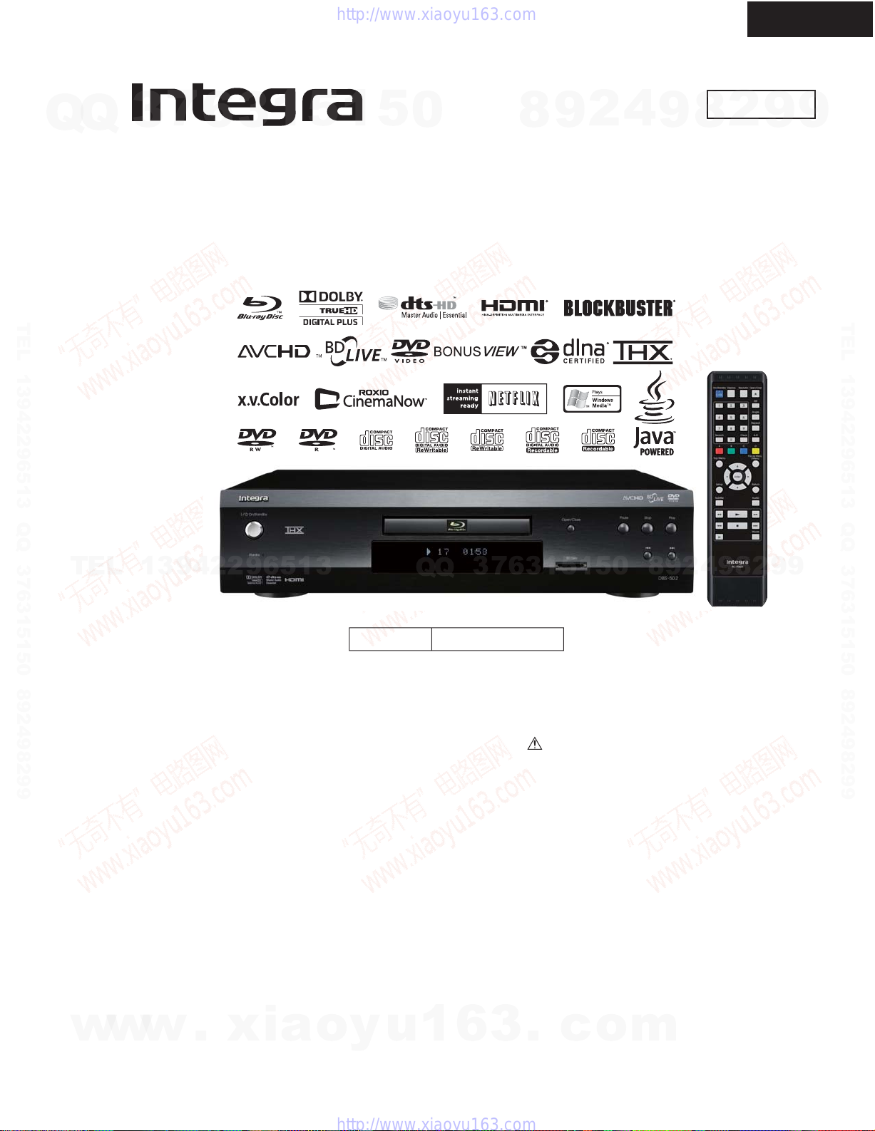
BLU-RAY DISC PLAYER
MODEL DBS-50.2(B)CDD1N
1
5
0
8
9
2
4
9
Sept, 2010
2
8
9
9
TEL 13942296513 QQ 376315150 892498299
TEL
13942296513
SAFETY-RELATED COMPONENT
WARNING!!
COMPONENTS IDENTIFIED BY MARK ON THE
SCHEMATIC DIAGRAM AND IN THE PARTS LIST ARE
CRITICAL FOR RISK OF FIRE AND ELECTRIC SHOCK.
REPLACE THESE COMPONENTS WITH ONKYO
PARTS WHOSE PART NUMBERS APPEAR AS SHOWN
IN THIS MANUAL.
MAKE LEAKAGE-CURRENT OR RESISTANCE
MEASUREMENTS TO DETERMINE THAT EXPOSED
PARTS ARE ACCEPTABLY INSULATED FROM THE
SUPPLY CIRCUIT BEFORE RETURNING THE
APPLIANCE TO THE CUSTOMER.
7
3
Q
Q
Black model
120V AC, 60HzB CDD1N
6
3
1
5
1
5
0
8
9
2
9
4
RC-794DV
8
2
9
9
w
w
w
.
xia
o
y
u
1
6
3
.
c
o
m
Page 2

TABLE OF CONTENTS
Specifications . . . . . . . . . . . . . . . . . . . . . . . . . . . . . . . . . . . . . . . . . . . . . . . . . . . . . . . . . . . . . . . . . . . . . . . . . . 1-1-1
7
Q
Q
Laser Beam Safety Precautions . . . . . . . . . . . . . . . . . . . . . . . . . . . . . . . . . . . . . . . . . . . . . . . . . . . . . . . . . . . . 1-2-1
Important Safety Precautions . . . . . . . . . . . . . . . . . . . . . . . . . . . . . . . . . . . . . . . . . . . . . . . . . . . . . . . . . . . . . . 1-3-1
Standard Notes for Servicing . . . . . . . . . . . . . . . . . . . . . . . . . . . . . . . . . . . . . . . . . . . . . . . . . . . . . . . . . . . . . .1-4-1
Cabinet Disassembly Instructions. . . . . . . . . . . . . . . . . . . . . . . . . . . . . . . . . . . . . . . . . . . . . . . . . . . . . . . . . . .1-5-1
How to Initialize the BLU-RAY Disc Player . . . . . . . . . . . . . . . . . . . . . . . . . . . . . . . . . . . . . . . . . . . . . . . . . . . . 1-6-1
Firmware Renewal Mode . . . . . . . . . . . . . . . . . . . . . . . . . . . . . . . . . . . . . . . . . . . . . . . . . . . . . . . . . . . . . . . . . 1-7-1
Home Network (DLNA) Error Code. . . . . . . . . . . . . . . . . . . . . . . . . . . . . . . . . . . . . . . . . . . . . . . . . . . . . . . . . . 1-8-1
Block Diagrams . . . . . . . . . . . . . . . . . . . . . . . . . . . . . . . . . . . . . . . . . . . . . . . . . . . . . . . . . . . . . . . . . . . . . . . . .1-9-1
Schematic Diagrams / CBA and Test Points . . . . . . . . . . . . . . . . . . . . . . . . . . . . . . . . . . . . . . . . . . . . . . . . . .1-10-1
TEL 13942296513 QQ 376315150 892498299
Exploded Views. . . . . . . . . . . . . . . . . . . . . . . . . . . . . . . . . . . . . . . . . . . . . . . . . . . . . . . . . . . . . . . . . . . . . . . .1-11-1
Mechanical Parts List . . . . . . . . . . . . . . . . . . . . . . . . . . . . . . . . . . . . . . . . . . . . . . . . . . . . . . . . . . . . . . . . . . . 1-12-1
Electrical Parts List . . . . . . . . . . . . . . . . . . . . . . . . . . . . . . . . . . . . . . . . . . . . . . . . . . . . . . . . . . . . . . . . . . . . . 1-13-1
3
6
3
1
5
1
5
0
8
9
2
4
9
8
2
9
9
TEL 13942296513 QQ 376315150 892498299
TEL
13942296513
Q
Q
3
7
6
3
1
5
1
5
0
8
9
2
4
9
8
2
9
9
w
w
w
.
xia
Manufactured under license from Dolby Laboratories.
Dolby and the double-D symbol are trademarks of Dolby Laboratories.
o
y
u
1
6
3
.
c
o
m
Page 3

SPECIFICATIONS
7
Q
Q
TEL 13942296513 QQ 376315150 892498299
3
6
3
1
5
1
5
0
8
9
2
4
9
8
2
9
9
TEL 13942296513 QQ 376315150 892498299
TEL
13942296513
Q
Q
3
7
6
3
1
5
1
5
0
8
9
2
4
9
8
2
9
9
w
w
w
.
xia
o
y
u
1
6
1-1-1 E5SF0SP
3
.
c
o
m
Page 4
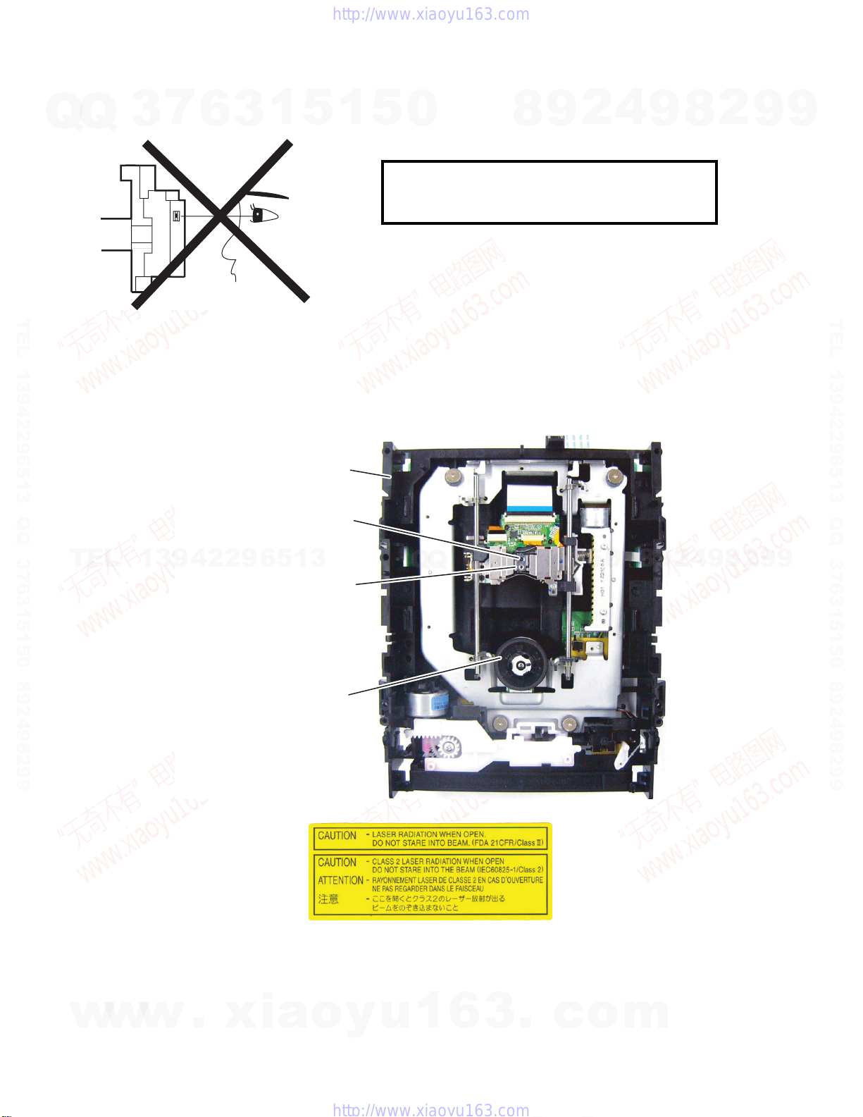
LASER BEAM SAFETY PRECAUTIONS
This BD player uses a pickup that emits a laser beam.
Q
Q
TEL 13942296513 QQ 376315150 892498299
The laser beam is emitted from the location shown in the figure. When checking the laser diode, be sure to keep
your eyes at least 30 cm away from the pickup lens when the diode is turned on. Do not look directly at the laser
beam.
CAUTION: Use of controls and adjustments, or doing procedures other than those specified herein, may result in
hazardous radiation exposure.
3
7
6
Drive Mechanism Assembly
Laser Beam Radiation
3
1
5
1
5
0
Do not look directly at the laser beam coming
from the pickup or allow it to strike against your
skin.
8
9
2
4
9
8
2
9
9
TEL 13942296513 QQ 376315150 892498299
TEL
13942296513
Laser Pickup
Turntable
Location: Inside Top of BD mechanism.
Q
Q
3
7
6
3
1
5
1
5
0
8
9
2
4
9
8
2
9
9
w
w
w
.
xia
o
y
u
1
6
1-2-1 B2NLBSP
3
.
c
o
m
Page 5

IMPORTANT SAFETY PRECAUTIONS
Product Safety Notice
Q
Q
Some electrical and mechanical parts have special
safety-related characteristics which are often not
evident from visual inspection, nor can the protection
they give necessarily be obtained by replacing them
with components rated for higher voltage, wattage,
etc. Parts that have special safety characteristics are
identified by a # on schematics and in parts lists. Use
of a substitute replacement that does not have the
same safety characteristics as the recommended
replacement part might create shock, fire, and/or other
TEL 13942296513 QQ 376315150 892498299
hazards. The Product’s Safety is under review
continuously and new instructions are issued
whenever appropriate. Prior to shipment from the
factory, our products are carefully inspected to confirm
with the recognized product safety and electrical
codes of the countries in which they are to be sold.
However, in order to maintain such compliance, it is
equally important to implement the following
precautions when a set is being serviced.
Precautions during Servicing
A. Parts identified by the # symbol are critical for
safety. Replace only with part number specified.
B. In addition to safety, other parts and assemblies
are specified for conformance with regulations
TEL
applying to spurious radiation. These must also be
replaced only with specified replacements.
Examples: RF converters, RF cables, noise
blocking capacitors, and noise blocking filters, etc.
C. Use specified internal wiring. Note especially:
1) Wires covered with PVC tubing
2) Double insulated wires
3) High voltage leads
D. Use specified insulating materials for hazardous
live parts. Note especially:
1) Insulation tape
2) PVC tubing
3) Spacers
4) Insulators for transistors
E. When replacing AC primary side components
(transformers, power cord, etc.), wrap ends of
wires securely about the terminals before
soldering.
F. Observe that the wires do not contact heat
producing parts (heat sinks, oxide metal film
resistors, fusible resistors, etc.).
G. Check that replaced wires do not contact sharp
edges or pointed parts.
H. When a power cord has been replaced, check that
w
w
5 - 6 kg of force in any direction will not loosen it.
7
3
13942296513
w
6
.
xia
3
1
5
o
1
y
5
u
I. Also check areas surrounding repaired locations.
0
J. Be careful that foreign objects (screws, solder
droplets, etc.) do not remain inside the set.
K. When connecting or disconnecting the internal
connectors, first, disconnect the AC plug from the
AC outlet.
L. When reassembling, be sure to use the original
screws or specified screws listed in the parts list.
7
3
Q
Q
1
6
3
6
8
3
.
9
1
1
5
c
2
5
o
4
0
m
9
8
9
8
2
4
2
9
8
9
2
9
9
TEL 13942296513 QQ 376315150 892498299
9
1-3-1 BDN_ISP
Page 6
Safety Check after Servicing
Examine the area surrounding the repaired location for damage or deterioration. Observe that screws, parts, and
wires have been returned to their original positions. Afterwards, do the following tests and confirm the specified
Q
Q
values to verify compliance with safety standards.
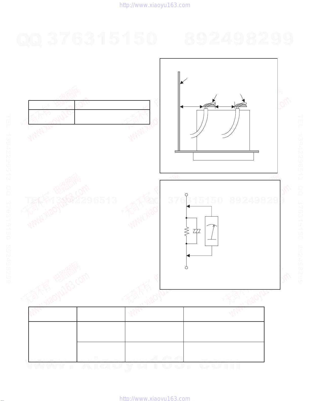
1. Clearance Distance
When replacing primary circuit components, confirm
specified clearance distance (d) and (d’) between
soldered terminals, and between terminals and
surrounding metallic parts. (See Fig. 1)
Table 1: Ratings for selected area
3
7
6
3
1
5
1
5
0
4
2
9
8
Chassis or Secondary Conductor
Primary Circuit
9
8
2
9
9
AC Line Voltage Clearance Distance (d), (d’)
TEL 13942296513 QQ 376315150 892498299
Note: This table is unofficial and for reference only. Be
2. Leakage Current Test
Confirm the specified (or lower) leakage current
between B (earth ground, power cord plug prongs) and
externally exposed accessible parts (RF terminals,
TEL
antenna terminals, video and audio input and output
terminals, microphone jacks, earphone jacks, etc.) is
lower than or equal to the specified value in the table
below.
Measuring Method (Power ON):
Insert load Z between B (earth ground, power cord plug
prongs) and exposed accessible parts. Use an AC
voltmeter to measure across the terminals of load Z.
See Fig. 2 and the following table.
120 V
sure to confirm the precise values.
13942296513
≥ 3mm(d)
≥ 4mm(d’)
Q
Q
3
7
d' d
Exposed Accessible Part
0
5
1
5
1
3
6
Z
One side of
B
Power Cord Plug Prongs
9
4
2
9
8
AC Voltmeter
(High Impedance)
Fig. 1
2
8
9
TEL 13942296513 QQ 376315150 892498299
9
Table 2: Leakage current ratings for selected areas
AC Line Voltage Load Z Leakage Current (i)
2kΩ RES.
Connected in
120 V
w
w
Note:This table is unofficial and for reference only. Be sure to confirm the precise values.
w
.
parallel
50kΩ RES.
Connected in
parallel
xia
o
i≤0.7mA AC Peak
i≤2mA DC
i≤0.7mA AC Peak
i≤2mA DC
y
u
1
6
3
1-3-2 BDN_ISP
One side of power cord plug
prongs (B) to:
Antenna terminals
A/V Input, Output
.
c
o
Fig. 2
RF or
m
Page 7
STANDARD NOTES FOR SERVICING
Circuit Board Indications
Q
Q
1. The output pin of the 3 pin Regulator ICs is
indicated as shown.
Out
2. For other ICs, pin 1 and every fifth pin are
indicated as shown.
TEL 13942296513 QQ 376315150 892498299
3. The 1st pin of every male connector is indicated as
shown.
3
Top Vi e w
Pin 1
Pin 1
7
6
In
3
Input
1
10
5
1
Bottom View
5
5
Pb (Lead) Free Solder
0
When soldering, be sure to use the Pb free solder.
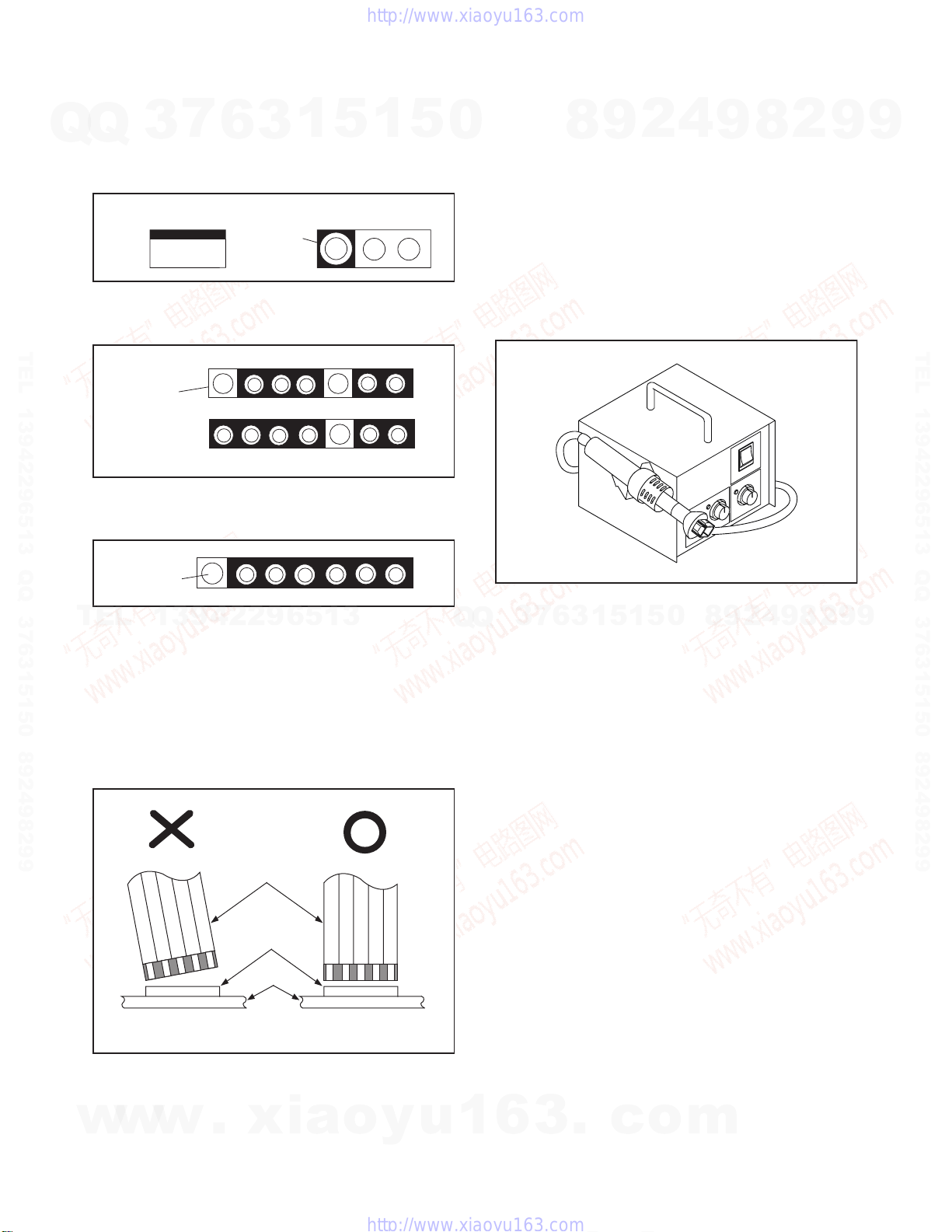
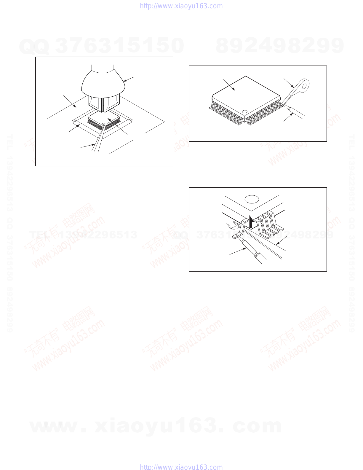
How to Remove / Install Flat Pack-IC
1. Removal
With Hot-Air Flat Pack-IC Desoldering Machine:
1. Prepare the hot-air flat pack-IC desoldering
machine, then apply hot air to the Flat Pack-IC
(about 5 to 6 seconds). (Fig. S-1-1)
8
9
2
4
9
8
Fig. S-1-1
2
9
9
TEL 13942296513 QQ 376315150 892498299
TEL
Instructions for Connectors
1. When you connect or disconnect the FFC (Flexible
2. FFC (Flexible Foil Connector) cable should be
13942296513
Foil Connector) cable, be sure to first disconnect
the AC cord.
inserted parallel into the connector, not at an
angle.
FFC Cable
Connector
CBA
* Be careful to avoid a short circuit.
2. Remove the flat pack-IC with tweezers while
7
3
Q
Q
applying the hot air.
3. Bottom of the flat pack-IC is fixed with glue to the
CBA; when removing entire flat pack-IC, first apply
soldering iron to center of the flat pack-IC and heat
up. Then remove (glue will be melted). (Fig. S-1-6)
4. Release the flat pack-IC from the CBA using
tweezers. (Fig. S-1-6)
CAUTION:
1. The Flat Pack-IC shape may differ by models. Use
an appropriate hot-air flat pack-IC desoldering
machine, whose shape matches that of the Flat
Pack-IC.
2. Do not supply hot air to the chip parts around the
flat pack-IC for over 6 seconds because damage
to the chip parts may occur. Put masking tape
around the flat pack-IC to protect other parts from
damage. (Fig. S-1-2)
6
3
1
5
1
5
0
8
9
2
4
9
8
2
9
9
w
w
w
.
xia
o
y
u
1
6
1-4-1 BDN_SN
3
.
c
o
m
Page 8
3. The flat pack-IC on the CBA is affixed with glue, so
be careful not to break or damage the foil of each
pin or the solder lands under the IC when
Q
TEL 13942296513 QQ 376315150 892498299
removing it.
Q
Masking
Ta pe
7
3
CBA
Tweezers
6
3
1
5
1
Hot-air
Flat Pack-IC
Desoldering
Machine
Flat Pack-IC
Fig. S-1-2
5
With Soldering Iron:
1. Using desoldering braid, remove the solder from
all pins of the flat pack-IC. When you use solder
0
flux which is applied to all pins of the flat pack-IC,
you can remove it easily. (Fig. S-1-3)
Flat Pack-IC
2. Lift each lead of the flat pack-IC upward one by
one, using a sharp pin or wire to which solder will
not adhere (iron wire). When heating the pins, use
a fine tip soldering iron or a hot air desoldering
machine. (Fig. S-1-4)
8
9
4
2
9
Desoldering Braid
Soldering Iron
8
Fig. S-1-3
2
9
9
TEL 13942296513 QQ 376315150 892498299
TEL
13942296513
Q
Fine Tip
Soldering Iron
3. Bottom of the flat pack-IC is fixed with glue to the
CBA; when removing entire flat pack-IC, first apply
soldering iron to center of the flat pack-IC and heat
up. Then remove (glue will be melted). (Fig. S-1-6)
4. Release the flat pack-IC from the CBA using
tweezers. (Fig. S-1-6)
Pin
Sharp
4
2
9
8
0
5
1
5
1
3
6
7
3
Q
2
8
9
Fig. S-1-4
9
9
w
w
w
.
xia
o
y
u
1
6
1-4-2 BDN_SN
3
.
c
o
m
Page 9
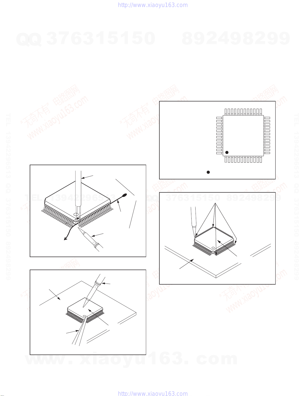
With Iron Wire:
1. Using desoldering braid, remove the solder from
all pins of the flat pack-IC. When you use solder
Q
TEL 13942296513 QQ 376315150 892498299
flux which is applied to all pins of the flat pack-IC,
Q
you can remove it easily. (Fig. S-1-3)
2. Affix the wire to a workbench or solid mounting
point, as shown in Fig. S-1-5.
3. While heating the pins using a fine tip soldering
iron or hot air blower, pull up the wire as the solder
melts so as to lift the IC leads from the CBA
contact pads as shown in Fig. S-1-5.
4. Bottom of the flat pack-IC is fixed with glue to the
CBA; when removing entire flat pack-IC, first apply
soldering iron to center of the flat pack-IC and heat
up. Then remove (glue will be melted). (Fig. S-1-6)
5. Release the flat pack-IC from the CBA using
tweezers. (Fig. S-1-6)
Note: When using a soldering iron, care must be
7
3
taken to ensure that the flat pack-IC is not
being held by glue. When the flat pack-IC is
removed from the CBA, handle it gently
because it may be damaged if force is applied.
6
1
3
Hot Air Blower
5
1
5
2. Installation
1. Using desoldering braid, remove the solder from
the foil of each pin of the flat pack-IC on the CBA
0
so you can install a replacement flat pack-IC more
easily.
2. The “ I ” mark on the flat pack-IC indicates pin 1.
(See Fig. S-1-7.) Be sure this mark matches the
pin 1 on the PCB when positioning for installation.
Then presolder the four corners of the flat pack-IC.
(See Fig. S-1-8.)
3. Solder all pins of the flat pack-IC. Be sure that
none of the pins have solder bridges.
Example :
Pin 1 of the Flat Pack-IC
is indicated by a " " mark.
8
9
2
4
9
8
Fig. S-1-7
2
9
9
TEL 13942296513 QQ 376315150 892498299
TEL
13942296513
To Solid
Mounting Point
CBA
Tweezers
Iron Wire
Soldering Iron
Fig. S-1-5
Fine Tip
Soldering Iron
Flat Pack-IC
or
Q
Q
3
CBA
7
6
3
1
1
5
Presolder
5
0
2
9
8
Flat Pack-IC
8
9
4
Fig. S-1-8
2
9
9
w
w
w
.
xia
Fig. S-1-6
o
y
u
1
6
1-4-3 BDN_SN
3
.
c
o
m
Page 10
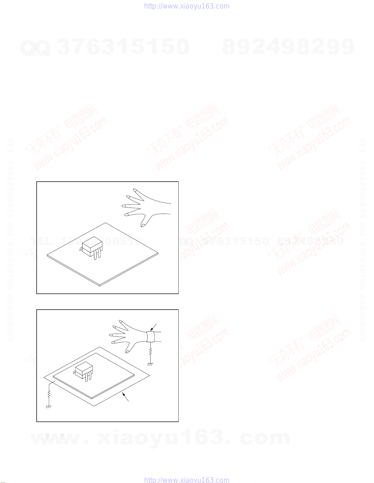
Instructions for Handling Semiconductors
7
Electrostatic breakdown of the semi-conductors may
Q
Q
occur due to a potential difference caused by
electrostatic charge during unpacking or repair work.
1. Ground for Human Body
Be sure to wear a grounding band (1 MΩ) that is
properly grounded to remove any static electricity that
may be charged on the body.
2. Ground for Workbench
Be sure to place a conductive sheet or copper plate
TEL 13942296513 QQ 376315150 892498299
with proper grounding (1 MΩ) on the workbench or
other surface, where the semi-conductors are to be
placed. Because the static electricity charge on
clothing will not escape through the body grounding
band, be careful to avoid contacting semi-conductors
with your clothing.
3
<Incorrect>
6
3
1
5
1
5
0
8
9
2
4
9
8
2
9
9
TEL 13942296513 QQ 376315150 892498299
TEL
<Correct>
13942296513
CBA
1MΩ
Conductive Sheet or
Copper Plate
CBA
Grounding Band
1MΩ
Q
Q
3
7
6
3
1
5
1
5
0
8
9
2
4
9
8
2
9
9
w
w
w
.
xia
o
y
u
1
6
1-4-4 BDN_SN
3
.
c
o
m
Page 11
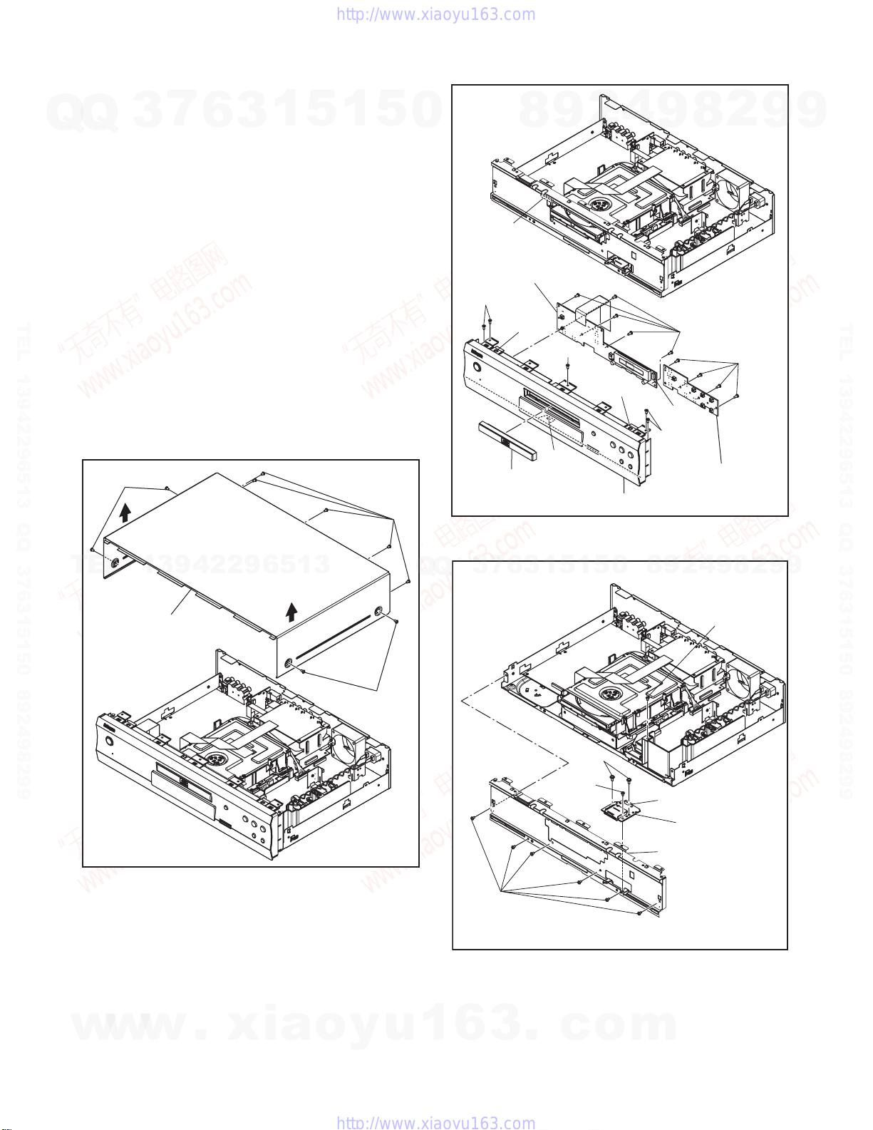
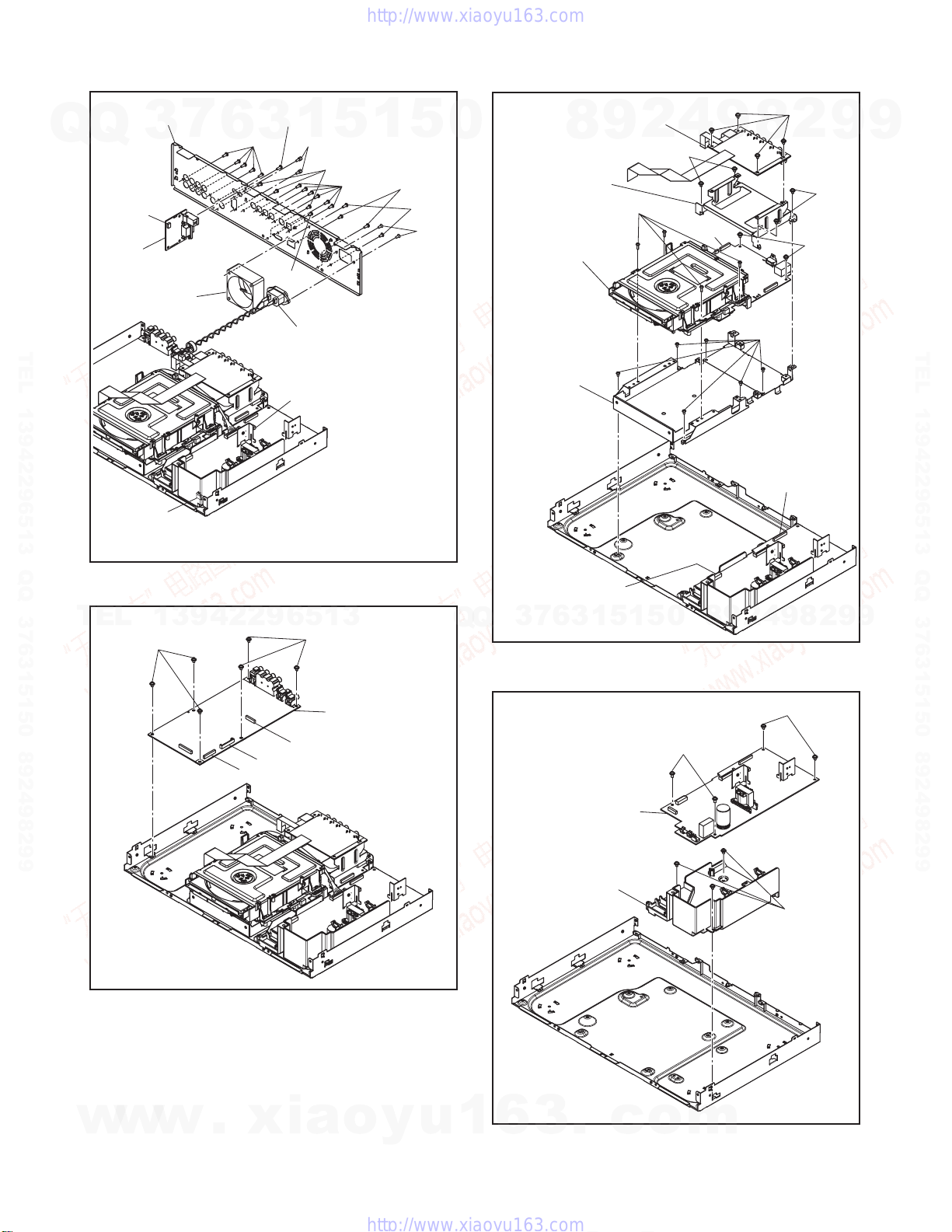
CABINET DISASSEMBLY INSTRUCTIONS
1. Disassembly Flowchart
Q
Q
This flowchart indicates the disassembly steps to gain
access to item(s) to be serviced. When reassembling,
follow the steps in reverse order. Bend, route, and
dress the cables as they were originally.
TEL 13942296513 QQ 376315150 892498299
[5] Front-B CBA
[7] SD CBA
[9] Motor
DC Fan
[12] Audio CBA
TEL
2. Disassembly Method
ID/
Loc.
No.
[1] Top Cover D1 9(S-1) --[2] Tray Panel D2 --------------- 1
[3]
[4]
[5]
[6]
[7]
[8]
[9]
[10]
w
w
7
3
13942296513
Part
Front
Assembly
Front-A
CBA
Front-B
CBA
Front
Bracket
SD CBA
AC Inlet
Motor DC
Fan
RS232C
w
CBA
6
[1] Top Cover
[2] Tray Panel
[3] Front
Assembly
[6] Front Bracket
[11] Rear Panel
[13] Video CBA
[14] AV PCB
Bracket
[15] BD Main CBA
& BD Mechanism
Assembly
[16] Loader
Bracket
Fig.
No.
D2
D2 *CN3001 ---
D2 --------------- ---
D3 7(S-4), (S-5) ---
D3 2(S-6), *CN5001 --D4 2(S-7), *CN1001 ---
D4 2(S-8), *CN1005 ---
D4
.
xia
1
3
Removal
Remove/*Unhook/
Unlock/Release/
Unplug/Desolder
*2(L-1), *(L-2), 5(S-2),
9(S-3), *CN2002
(S-9), 2(S-10),
*CN5501
5
1
[4] Front-A CBA
[8] AC Inlet
[10] RS232C
CBA
[17] Power
Supply CBA
[18] Power
Holder
o
y
5
Note
u
2
---
0
Q
1
ID/
Loc.
No.
[11] Rear Panel D4
[12] Audio CBA D5
[13] Video CBA D6 4(S-15), *CN7101 ---
[14]
[15]
[16]
[17]
[18]
↓
(1)
7
3
Q
Note:
(1) Identification (location) No. of parts in the figures
(2) Name of the part
(3) Figure Number for reference
(4) Identification of parts to be removed, unhooked,
unlocked, released, unplugged, unclamped, or
desoldered.
P = Spring, L = Locking Tab, S = Screw,
CN = Connector
* = Unhook, Unlock, Release, Unplug, or Desolder
e.g. 2(S-2) = two Screws (S-2),
2(L-2) = two Locking Tabs (L-2)
(5) Refer to “Reference Notes.”
6
3
9
8
Part
AV PCB
Bracket
BD Main
CBA & BD
Mechanism
Assembly
Loader
Bracket
Power
Supply
CBA
Power
Holder
↓
(2)
5
1
3
6
.
c
2
Fig.
No.
11(S-11), (S-12),
5(S-13)
6(S-14), *CN2005,
*CN2007, *CN2008
D6 4(S-16) ---
2(S-17), 4(S-18),
D6
*CN1003, *CN1100
D6 6(S-19) ---
D7 2(S-20), 2(S-21) ---
D7 3(S-22) ---
↓
(3)
0
5
1
o
9
Remove/*Unhook/
Unlock/Release/
Unplug/Desolder
↓
(4)
2
9
8
m
Removal
4
8
4
2
9
8
9
Note
2
4
---
3
↓
(5)
9
9
TEL 13942296513 QQ 376315150 892498299
9
1-5-1 E5SF0DC
Page 12
Reference Notes
1. How to remove tray panel
Q
TEL 13942296513 QQ 376315150 892498299
1) Connect the wall plug to an AC outlet and press
Q
2) Lift up and remove the tray panel.
3) Press the [ Open/Close] button again to close
4) Press the [On/Standby] button to turn the
5) Unplug the AC cord.
2. CAUTION 1: Locking Tabs (L-1) and (L-2) are
fragile. Be careful not to break them.
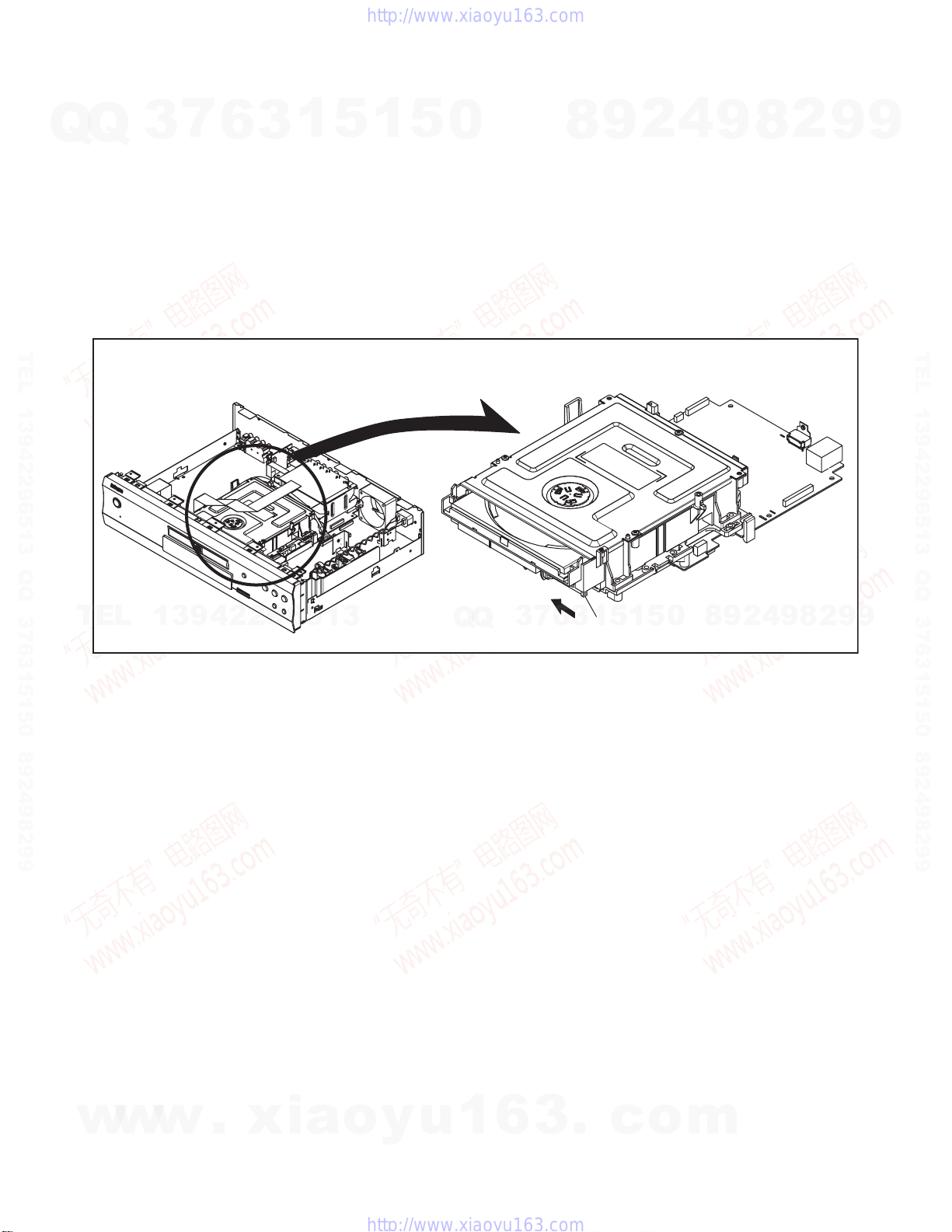
3. The BD Main CBA & BD Mechanism Assembly
is adjusted as a unit at factory. Therefore, do
not disassemble it. Replace the BD Main CBA
& BD Mechanism Assembly as a unit.
4. When reassembling, be sure to use the original
screws or specified screws listed in the parts
list.
7
3
the [ Open/Close] button to open the tray.
the tray.
power off.
6
3
1
5
1
5
0
CN2002
[4] Front-A CBA
(S-2)
8
(L-1)
9
(S-2)
2
4
(L-1)
8
9
(S-3)
CN3001
(S-2)
2
(S-3)
9
9
TEL 13942296513 QQ 376315150 892498299
(S-1)
TEL
13942296513
[1] Top Cover
(S-1)
(S-1)
Fig. D1
Q
Q
(L-2)
[2] Tray Panel
1
3
6
7
3
[3] Front Assembly
8
0
5
1
5
(S-6)
(S-5)
[5] Front-B CBA
Fig. D2
2
8
9
4
2
9
(S-4)
CN5001
[7] SD CBA
[6] Front Bracket
9
9
w
w
w
.
xia
(S-4)
o
y
u
1
6
1-5-2 E5SF0DC
3
.
c
o
Fig. D3
m
Page 13
[11] *Rear Panel
7
Q
Q
CN5501
TEL 13942296513 QQ 376315150 892498299
3
[10] RS232C
CBA
[9] Motor
DC Fan
CN1001
*See Reference Note 4.
6
3
(S-11)
(S-9)
1
(S-10)
(S-12)
[8] AC Inlet
CN1005
5
(S-13)
(S-11)
1
5
(S-13)
(S-8)
(S-7)
Fig. D4
0
[14] AV PCB
Bracket
[15] *BD Main CBA
& BD Mechanism
Assembly
[16] Loader
Bracket
[13] Video CBA
8
9
(S-18)
2
(S-16)
4
CN7101
9
8
(S-19)
CN1003
(S-15)
2
(S-17)
9
(S-16)
9
TEL 13942296513 QQ 376315150 892498299
TEL
13942296513
(S-14)
CN2008
CN2005
(S-14)
CN2007
[12] Audio CBA
Fig. D5
Q
CN1100
1
3
6
7
3
Q
* See Reference Note 3.
[17] Power Supply
CBA
[18] Power Holder
5
1
5
0
(S-20)
8
9
2
9
4
(S-21)
8
Fig. D6
(S-22)
2
9
9
w
w
w
.
xia
o
y
u
1
6
1-5-3 E5SF0DC
3
.
c
o
Fig. D7
m
Page 14
3. How to Eject a Disc
When a disc cannot be removed due to malfunction or when an unplayable disc is inserted, follow the
procedure below to remove the disc.
Q
Q
Procedure A
1. Unplug the AC power cord and then plug it in.
2. Turn the power on by pressing the [Open/Close] button and the disc tray will open automatically.
Procedure B
1. Remove the Top Cover.
2. Slide the portion A in the direction of the arrow.
3. Pull the tray out manually and remove the disc.
3
7
6
3
1
5
1
5
0
8
9
2
4
9
8
2
9
9
TEL 13942296513 QQ 376315150 892498299
TEL
13942296513
Q
Q
3
7
6
1
3
Portion A
5
1
5
0
8
9
2
4
9
8
2
9
TEL 13942296513 QQ 376315150 892498299
9
w
w
w
.
xia
o
y
u
1
6
1-5-4 E5SF0DC
3
.
c
o
m
Page 15
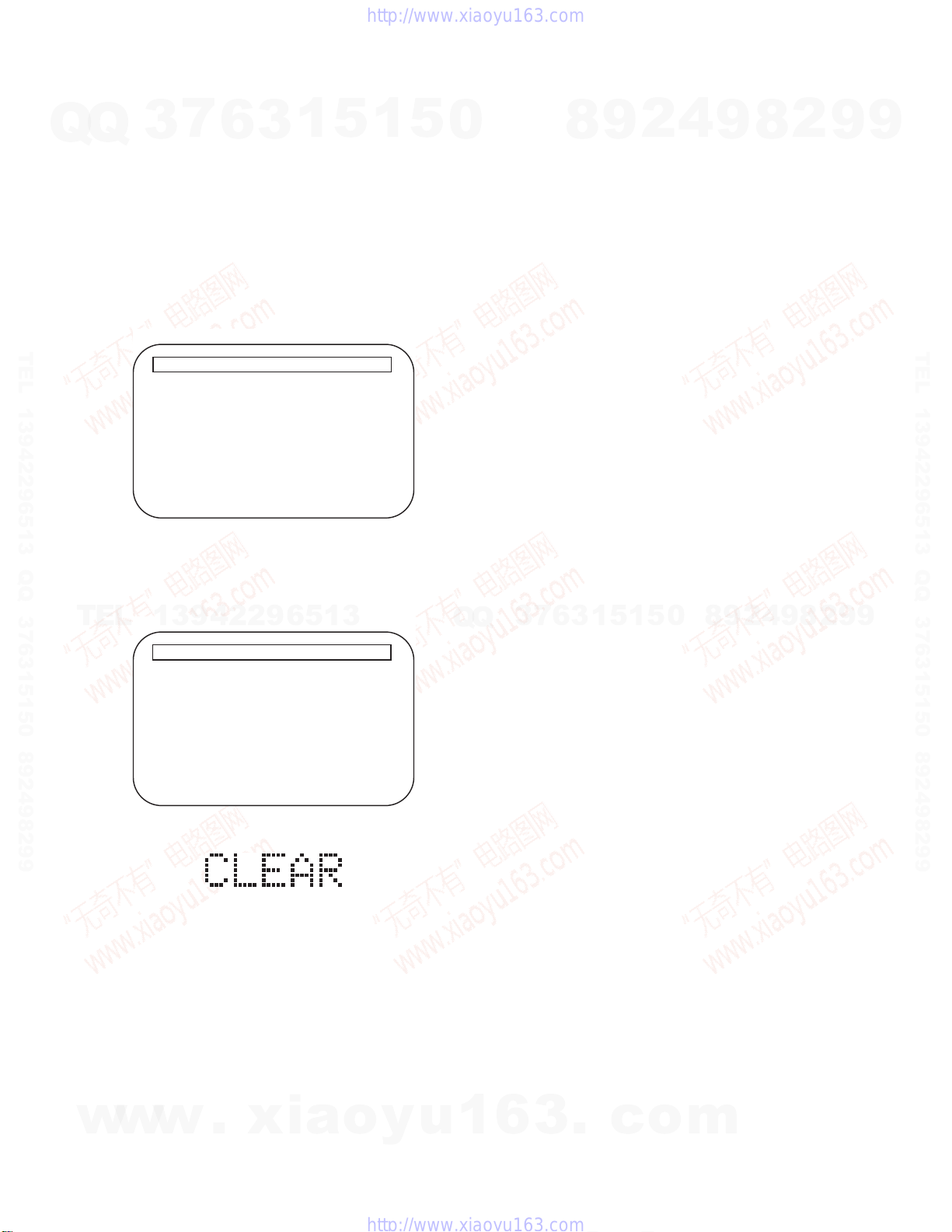
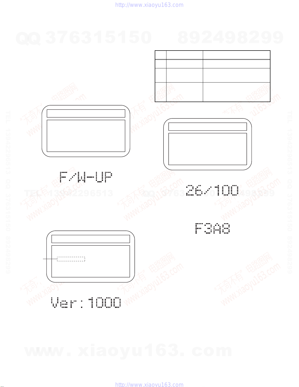
HOW TO INITIALIZE THE BLU-RAY DISC PLAYER
To put the program back at the factory-default,
Q
Q
initialize the BD player as the following procedure.
Note: By initializing, network is reset to disconnected
1. Turn the power on.
2. Remove the disc on the tray and close the tray.
3. Press [1], [2], [3], [4], and [Display] buttons on the
remote control unit in that order.
Fig. a appears on the screen.
TEL 13942296513 QQ 376315150 892498299
4. Press [ C ] button on the remote control unit.
Fig. b appears on the screen and Fig. c appears
on the VFD.
TEL
7
3
state and “Network Service Disclaimer”
appears on the screen.
Version Info
F/W Name
Version
Region
Pickup
ESN
DRM
13942296513
Version Info
6
"
*******
: *******
: *.***
: *-*
: **
: ***********************************
: OK
"
*******
1
5
3
" differ depending on the models.
EXIT <POWER>EEPROM CLEAR <STOP>
Fig. a
" differ depending on the models.
1
5
0
Q
Q
3
7
6
8
3
9
1
5
1
2
5
4
0
9
8
9
8
2
4
2
9
8
9
2
9
9
TEL 13942296513 QQ 376315150 892498299
9
F/W Name
Version
Region
Pickup
ESN
DRM
EEPROM CLEAR : OK
5. To exit this mode, press [On/Standby] button.
w
w
w
: *******
: *.***
: *-*
: **
: ***********************************
: OK
EXIT <POWER>EEPROM CLEAR <STOP>
Fig. b
Fig. c
.
xia
o
y
u
1
6
3
.
c
o
m
1-6-1 E5SF1INT
Page 16
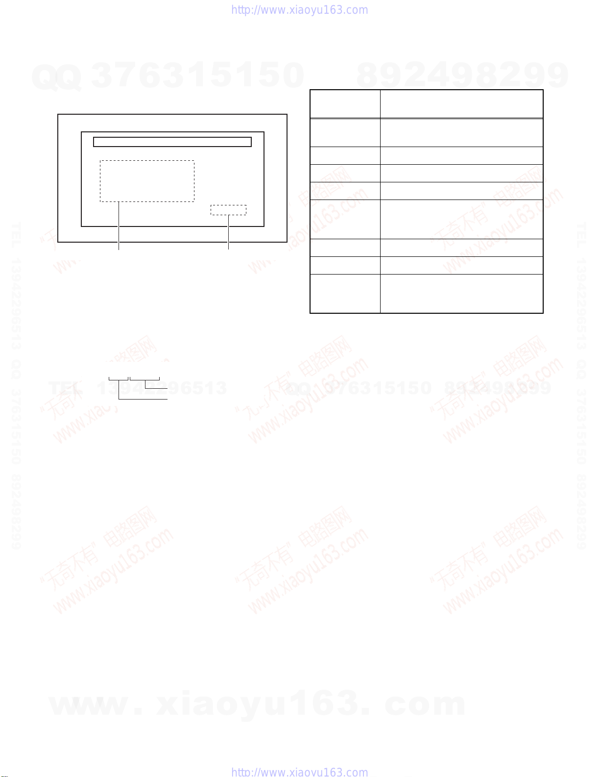
FIRMWARE RENEWAL MODE
Note: The file extension of the available firmware is
Q
Q
1. Turn the power on and remove the disc on the tray
and close the tray.
2. To put the BD player into version up mode, press
[9], [8], [7], [6], and [Pop-Up Menu/Menu] buttons
on the remote control unit in that order. The tray
will open automatically.
Fig. a appears on the screen and Fig. b appears
on the VFD.
TEL 13942296513 QQ 376315150 892498299
7
3
“b35”.
F/W VERSION UP MODE F/W Name: ******* Ver. *.***
Please Insert a Disc
Fig. a Version Up Mode Screen
6
"
*******
for F/W Version Up
1
3
" differs depending on the models.
5
1
5
0
The appearance shown in (*1) of Fig. c is
described as follows:
No. Appearance State
1 Now Loading... Loading the disc
2 Reading...
3 See FL Display.
4
2
9
8
Sending files into the
memory.
Writing new version data,
the progress will be displayed
as shown in Fig. f.
"
" differ depending on the models.
*******
F/W VERSION UP MODE F/W Name: ******* Ver. *.***
1. ALL
Version : *.*** **************.b35
CHECKSUM : ****
See FL Display.
EXIT : POWER
Fig. e Version Up Mode
9
8
2
9
9
TEL 13942296513 QQ 376315150 892498299
Fig. b VFD in Version Up Mode
TEL
3. Load the disc for version up.
4. The BD player enters the F/W version up mode
13942296513
automatically. Fig. c appears on the screen and
Fig. d appears on the VFD. Make sure to insert the
proper F/W for the state of this model.
"
" differ depending on the models.
*******
F/W VERSION UP MODE F/W Name: ******* Ver. *.***
(*1)
Fig. c Programming Mode Screen (Example)
Fig. d VFD in Programming Mode (Example)
Now Loading...
4
2
9
8
0
5
1
5
1
3
6
7
3
Q
Q
Fig. f VFD in Version Up Mode
5. After programming is finished, the checksum on
the VFD (Fig. g).
Fig. g
VFD upon Finishing the Programming Mode (Example)
Checksum appears on the VFD then the tray will
open automatically. Remove the disc on the tray.
At this time, no button is available.
6. Unplug the AC cord from the AC outlet. Then plug
it again.
7. Turn the power on.
Note: All the settings will be put back to factory-
default.
9
8
2
9
9
w
w
w
.
xia
o
y
u
1
6
1-7-1 E5SF1FW
3
.
c
o
m
Page 17
How to Verify the Firmware Version
1. Turn the power on.
2. Remove the disc on the tray and close the tray.
Q
Q
3. Press [1], [2], [3], [4], and [Display] buttons on the
remote control unit in that order.
Fig. h appears on the screen.
7
3
Version Info
6
"
*******
1
3
" differ depending on the models.
5
1
5
0
8
9
2
4
9
8
2
9
9
F/W Name
Version
Region
Pickup
ESN
TEL 13942296513 QQ 376315150 892498299
4. To exit this mode, press [On/Standby] button.
TEL
DRM
13942296513
: *******
: *.***
: *-*
: **
: ***********************************
: OK
EXIT <POWER>EEPROM CLEAR <STOP>
Fig. h
Q
Q
3
7
6
3
1
5
1
5
0
8
9
2
4
9
8
2
9
TEL 13942296513 QQ 376315150 892498299
9
w
w
w
.
xia
o
y
u
1
6
1-7-2 E5SF1FW
3
.
c
o
m
Page 18
HOME NETWORK (DLNA) ERROR CODE
Error Code appears in the error screen when the unit
Q
Q
detects an error, as shown below. The code is used to
specifically determine the cause of error.
TEL 13942296513 QQ 376315150 892498299
Error Code are displayed with “ ******** ” (“*” is error
code) as shown above.
Error Code Form
In the Home Network (DLNA), Error Code are used as
follows.
002XXXXX
7
3
Cannot connect to server.
Please check your settings.
Press ‘ENTER’.
Error message
6
Network Error
Fig. 1: Error Code (Example)
3
1
5
1
00202010
Error Code
5
“Summary Error Code” are shown in the list below.
0
Summary
Error Code
4
2
9
8
Error message
02
03 Playback Error
05 No playable files found.
20 System Error
21
22 List Updated.
23 Connection with server lost.
24
Cannot connect to server. Please
check your settings.
Unable to display files from the
server. Please check server
settings.
Unable to connect to more than 10
servers. Please turn off or stop
broadcasting 1 or more servers.
9
8
2
9
9
TEL 13942296513 QQ 376315150 892498299
TEL
13942296513
Detailed Error Code
Summary Error Code
Fig. 2
Q
Q
3
7
6
3
1
5
1
5
0
8
9
2
4
9
8
2
9
9
w
w
w
.
xia
o
y
u
1
6
1-8-1 E5SF1ER
3
.
c
o
m
Page 19

Detailed Error Code table (DLNA – HTTP Status Code)
Status Code Description
7
3
Q
TEL 13942296513 QQ 376315150 892498299
201 Created A new resource was created by this unit’s request.
Q
202 Accepted This unit’s request was accepted but its processing is not completed.
204 No Content Though the server processed the request, there was no content.
205 Reset Content No content.
300 Multiple Choices
301 Moved Permanently
6
3
1
5
1
5
0
• There are multiple choices.
• The server could not determine its response.
• Requested information contains multiple representations.
This status is handled as Redirection by default and complies with the content
of Location HEAD related to this response.
• Moved Permanently.
• Requested resource has been assigned to a new permanent URI (Uniform
Resource Identifier). Any future references to this source must use one of the
returned URIs.
• Indicates that requested information is moved to the URI specified by the
Location HEAD. When this status is received, the default action is tracking
the Location HEAD related to the response. When the original request
method is POST, the redirected request will use GET.
8
9
2
4
9
8
2
9
9
TEL 13942296513 QQ 376315150 892498299
• Found.
• Requested resource resides temporarily under a different URI.(Uniform
Resource Identifier)
302 Found
TEL
13942296513
303 See Other
304 Not Modified
305 Use Proxy
400 Bad Request The server could not understand this unit’s request.
401 Unauthorized Indicates that the resource requested by this unit requires authentication.
403 Forbidden The server received this unit’s request, but refused to fulfill it.
• Indicates that requested information exists in the URI specified by the Location HEAD. When this status is received, Location HEAD related to the
response will be tracked by default. When the request method is POST the
redirected request will use GET.
• See other.
• The response to the request can be found under a different URI (Uniform
Resource Identifier) and to get this response, GET HTTP method will be
used.
• As a result of POST, client will be automatically redirected to the URI specified by the Location HEAD. GET will be used for requesting to a resource
specified by the Location HEAD.
This unit caches the latest resource and the requested resource is not
modified. (exception protocol error)
• Proxy will be used.
• The requested resource must be accessed through the proxy specified by the
Location field.
• Indicates that request must use the URI given by the Location HEAD to use
the proxy server.
Q
Q
3
7
6
3
1
5
1
5
0
8
9
2
4
9
8
2
9
9
404 Not Found The requested URI was not found.
• The method is not allowed.
405 Method Not Allowed
406 Not Acceptable
w
w
w
.
xia
• The HTTP behavior used is not allowed.
• Indicates that request method (POST or GET) is not allowed by the
requested resource.
• The client could not find an acceptable response.
• Indicates that the client specifies not to accept arbitrary representation for
Accept header which could be used by the resource.
o
y
u
1
1-8-2 E5SF1ER
6
3
.
c
o
m
Page 20

Status Code Description
407 Proxy Authentication
Required
7
Q
Q
TEL 13942296513 QQ 376315150 892498299
3
408 Request Timeout
409 Conflict
410 Gone
411 Length Required
412 Precondition Failed
6
3
• Proxy authentication is required.
• Indicates that the requested proxy will request authentication. Proxy-authenti-
1
5
1
5
cate header contains the detailed method for authentication.
• While waiting for request, the server timed out.
• Indicates that the client did not send a request within the expected time by
the server.
• There is a conflict.
• The server timed out while waiting for a request.
• Indicates that the client did not send a request within the expected time by
the server.
• No longer available.
• The requested resource could not be found at the server and forwarding
address is unknown.
• Indicates that requested resource is no longer available.
• Length required.
• The server refused to accept the request where Content-Length was undefined.
• Indicates Content-length header is not defined.
• Fails to fulfill precondition.
• The precondition in one or more of the requested header field has been
tested false by the server.
• The precondition given in the request could not be fulfilled and the request
failed. Precondition can be set using If-Match, If-None-Match, If-UnmodifiedSince request header.
0
8
9
2
4
9
8
2
9
9
TEL 13942296513 QQ 376315150 892498299
• The requested entity is too large.
413 Request Entity Too
TEL
Large
13942296513
414 Request-URI Too Long
415 Unsupported Media
Ty pe
500 Internal Server Error Internal server error occurred.
501 Not Implemented
502 Bad Gateway
503 Service Unavailable
504 Gateway Timeout
• The server refused to process the request since the requested entity is larger
than the server is willing or able to process.
• Indicates that the request is too large for the server to process.
• The Request-URI is too long.
• The server refused to process the request because the request URI (Uniform
Resource Identifier) is too long for the server to interpret.
• Indicates that the URI is too long.
• The media type is not supported.
• The server refused to process the request because the format of request
entity is not supported by the requested resource for the requested method.
• Indicates the requested format is not supported.
The server does not support functionalities required to process the request
from this unit.
The proxy server between this unit and the server received an invalid reply from
another proxy or the original server.
• Service is unavailable.
• The service is temporarily overloaded.
• Because of overloading or maintenance, the server is temporarily unavailable.
• Gateway timed out.
• While waiting for gateway, the request timed out.
• Indicates that the intermediate proxy server has timed out while waiting for a
response from another proxy or original server.
Q
Q
3
7
6
3
1
5
1
5
0
8
9
2
4
9
8
2
9
9
505 Version Not Supported
w
w
w
.
• The version is not supported.
• The server refuses or does not support the version of protocol given in the
xia
• Indicates that requested version is not supported by the server.
request message.
o
y
u
1
6
1-8-3 E5SF1ER
3
.
c
o
m
Page 21

Detailed Error Code table (DLNA – Application Status Code)
Status Code Description
Q
7
Q
3
001 Nothing List
010 LAN Disconnect This unit’s LAN is disconnected.
020 Application Status Error Error was detected in the DLNA application’s internal state.
021 Application Status Error Error was detected in the DLNA application’s internal state.
022 Application System Error Error was detected in the DLNA application system.
023 Unsupported Audio
Format
6
3
1
5
1
5
As a result of list creation process, there is no item to be displayed from the
received data.
An unsupported audio format was discovered.
0
8
9
2
4
9
8
2
9
9
024 Server Number Over
TEL 13942296513 QQ 376315150 892498299
TEL
Limit
025 Changed List The contents list currently displayed has been updated.
026 Disconnected Server The original server of the displaying contents list has been disconnected.
027 Application System Error Error was detected upon start of DLNA application.
600 Disconnected Server The original server of the contents has been disconnected.
601 Not Exist Content Content does not exist.
602 Critical Error System error.
603 Changed List The contents list has been updated at the server.
620 Not Exist Content Image content does not exist.
621 Get failure Image data get error. (an error other than HTTP status and under 500s)
622 File Open Error Image data working file open error.
13942296513
623 File Read Error Image data working file read error.
624 File Close Error Image data working file close error.
625 Decode mode Error Image data decode mode error.
626 Header Error Image data header error.
627 Struct Error Image data header structural error.
628 Decode Error Image data decode error.
Discovered server numbers over limit.
7
3
Q
Q
6
3
1
5
1
5
0
8
9
2
4
9
8
2
9
TEL 13942296513 QQ 376315150 892498299
9
629 Unsupported Format Unsupported format.
630 Unsupported Size Unsupported data size.
631 Attach Error Shared memory attach error.
632 Detach Error Shared memory detach error.
633 Server Time Out Error Server timed out.
640 File Read Error File read error.
641 Unsupported Format Unsupported Format.
642 No Change Decode
Frame
643 Stream Get Error Stream get error.
660 File Read Error File read error.
661 Unsupported Format Unsupported format.
662 Video Analyze Error Video analyze error.
w
w
w
663 Audio Analyze Error Audio analyze error.
.
xia
No updates of decode frame.
o
y
u
1
6
3
.
c
o
m
1-8-4 E5SF1ER
Page 22

Q
Status Code Description
664 1sec Offset Get Error 1sec offset get error.
665 Address Search Error Address search error.
Q
680 RFS_EVENT_SOCKET_
681 RFS_EVENT_HTTP_
682 RFS_EVENT_HTTP_
7
3
ERROR
RES_SERVER_
REFUSED
RES_NOT_FOUND
6
3
1
5
1
5
Socket error.
Server refusal notification.
The specified contents could not be found.
0
8
9
2
4
9
8
2
9
9
683 RFS_EVENT_HTTP_
RES_SERVER_ERROR
TEL 13942296513 QQ 376315150 892498299
684 RFS_EVENT_HTTP_
RES_UNEXPECTED_
CODE
685 RFS_EVENT_HTTP_
RES_RANGE_NOT_
SATISFIABLE
686 RFS_EVENT_RECV_
TIMEOUT
687 RFS_EVENT_DTCP_
ERROR
688 RFS_EVENT_DTCP_
CONNECT_ERROR
689 RFS_EVENT_DTCP_
TEL
KEY_MNG_ERROR
13942296513
690 RFS_EVENT_
RESPONSE_DATA_
ERROR
691 RFS_EVENT_SYSTEM_
ERROR
692 RFS_EVENT_TCP_
DISCONNECTED
693 RFS_EVENT_
CONNECT_TIMEOUT
Server error.
Unexpected status code.
The specified range is not satisfiable.
Timed out while waiting for response.
RCVC internal error. (DTCP originated)
DTCP connection error.
Kx key error.
Received message is invalid.
RCVC internal error.
The TCP connection has been disconnected by the server during streaming.
Time out occurred while establishing TCP connection.
Q
Q
3
7
6
3
1
5
1
5
0
8
9
2
4
9
8
2
9
TEL 13942296513 QQ 376315150 892498299
9
694 RFS_EVENT_RECV_
ERROR
700 Refresh Error Failed to update server list.
701 Disconnected Server The server has been disconnected while displaying contents list.
702 Server Not Found The server has been disconnected while getting contents list.
703 Server Info Error Failed to get server information while getting contents list.
704 Contents List Error Failed to get contents list.
705 Server Config Error Failed to configure server.
706 List Not Found Failed to get contents list.
707 Changed List Displayed contents list has been updated.
708 Object Not Found Neither folders or playable contents was found.
709 Object Not Found By
w
w
w
Filter
.
xia
Could not receive contents.
Playable contents was not found by filter.
o
y
u
1
6
3
.
1-8-5 E5SF1ER
c
o
m
Page 23

Q
Status Code Description
710 Object Count Zero Nothing was found in the folder.
711 ILLEGAL Server Info The contents information from the server is invalid.
Q
712 ILLEGAL Total Count The total counts of contents from the server is invalid.
3
7
6
3
1
5
1
5
0
8
9
2
4
9
8
2
9
9
713 Folder not Exist
714 Critical Error An error occurred on the system.
TEL 13942296513 QQ 376315150 892498299
TEL
13942296513
The specified folder does not exist. (The current contents list displayed has
been updated)
7
3
Q
Q
6
3
1
5
1
5
0
8
9
2
4
9
8
2
9
TEL 13942296513 QQ 376315150 892498299
9
w
w
w
.
xia
o
y
u
1
6
1-8-6 E5SF1ER
3
.
c
o
m
Page 24

BLOCK DIAGRAMS
System Control Block Diagram
7
Q
Q
3
VIDEO CBA
TEL 13942296513 QQ 376315150 892498299
(SUB MICRO CONTROLLER)
IC2000
6
TO VIDEO
BLOCK DIAGRAM
VIDEO-MUTE
CN4001
1818
VIDEO-MUTE
CN2005
23VIDEO-MUTE
XOUT
9
XIN
11
3
PWSW1
1
TO POWER SUPPLY
BLOCK DIAGRAM
PWSW3
PWSW2
FAN-LOCK
FAN-CONT1
17
40
PWSW116PWSW215PWSW3
FAN-LOCK
CEC-IN32CEC-OUT
31
5
CEC-CONT
6
22
CEC-CONT
FAN-CONT1
1
TO AUDIO
BLOCK DIAGRAM
AUDIO-MUTE
7AUDIO-MUTE
5
SUB-TXD
SUB-RXD
48
47
0
FRONT-A CBA
SYS-RESET
20
RS3001
VFD
19 20 21 22
FL3001
CN3002
CN2002
SENSOR
REMOTE
345
FL-SDA
FL-SCL
345
29
28
FL-SCL
FL-SDA
8
6
FL-STB
FL-RESET
6
27
26
FL-STB
FL-RESET
9
EV+3.3V
121716
-LED
REMOTE
STANDBY
121716
30
44
REMOTE
STANDBY-LED
SW3008
KEY-1
42
KEY-1
4
2
Q3001
D3002
STANDBY
CN3001 CN3101
POWER
2 2
KEY-1
RS232C-RXD
33
9
34 RS232C-TXD
21 232C-PW-CONT
8
KEY
SWITCH
2
FRONT-B CBA
AUDIO CBA
9
9
TEL 13942296513 QQ 376315150 892498299
TEL
CN2005
13
CEC-IN
13
CN4001
CN4000
13CEC-IN
13
CN7101
SWITCHING
Q7504, Q7505
BUFFER
Q7503
Q7502
14
14 CEC-OUT
14
14 CEC-OUT
BUFFER
10MHz
13942296513
BD MAIN CBA
X2000
X'TAL
IC6001
(MAIN MICRO CONTROLLER)
CN2005
10
SUB-TXD
101010
CN4001
SUB-TXD
CN7101 CN4000
U34
RXD1
9
11
SUB-RXD
SYS-RESET
11
99
1111 9
SUB-RXD
SYS-RESET
V32
TXD1
Q
Q
T34
XRST
A27
AE32
XTRST
XFERST
3
Q6702
7
6
IC6701
3
Q6701
RESET
2 1
1
5
1
RS232C CBA
5
IC5500
0
EV+5V
Q5500,Q5501
RS232C
INTERFACE
123
CN2005CN4002 CN4001CN5501
8
RS232C-RXD
RS232C-TXD
12333
4
5
RS232C-RXD
RS232C-TXD
4
5
SWITCHING
11
12
16
VCC
RS232C
I/F
13
14
66
9
RS232C-PW-CONT
REMOTE
11
RS232C-PW-CONT
REMOTE
IC5550
2
PHOTO
COUPLER
JK5550
9
4
BUFFER
Q5551,Q5552
3
4
1
2
8
9
9
2
VIDEO CBA
w
w
w
.
xia
JK7501
HDMI-
CONNECTOR
13
CEC
o
y
u
1
6
1-9-1
3
P-ON+1.8V
.
c
o
2TXD
3RXD
CN5500
m
RS232C-
CONNECTOR
REMOTE
-OUT
REMOTE
-IN
E5SF0BLS
Page 25

Digital Signal Process 1 Block Diagram
7
Q
Q
3
VIDEO SIGNAL AUDIO SIGNAL
TEL 13942296513 QQ 376315150 892498299
6
TO DIGITAL SIGNAL
PROCESS 2 BLOCK
STREAM
FE
DIGITAL
3
DIAGRAM
(IC6001)
CONTROL
SIGNAL
PROCESS
1
5
1
TRACKING-CONTROL
E23
5
FOCUS1-CONTROL
A24
0
COPY
PROTECT
AACS
FOCUS2-CONTROL
D23
BD+
CSS
CPRM
EXPA-CONTROL
B22
EXPB-CONTROL
D22
8
SLED1-CONTROL
C24
9
SLED2-CONTROL
D24
2
LOAD-CONTROL
C22
4
TRAY-OUT
TRAY-IN
E217E24
D21
9
SPINDLE-CONTROL
8
SPINDLE-FG
B25
2
9
9
TEL 13942296513 QQ 376315150 892498299
TEL
13942296513
(MAIN MICRO CONTROLLER/DIGITAL SIGNAL PROCESS)
IC6001
MPX
WOB
MATRIX
B31,C31
A32,B32,
A30,A31,
Q101
*1: 14, 16, 18, 26
*2: 13, 15, 27, 29
CN101
A-D *1
E-H *2
BUFFER
/LPP
B30,C30
Q102
BUFFER
RF(-) 21
RF(+) 20
RF
EQUALIZER
RF
GENERATOR
SD ATA 2
SCLK2
B34
C33
G30
G31
M32
M31
SCLK2 39
SD ATA 2 3 8
BDRF(-) 24
BDRF(+) 23
27
TRACKING
ACTUATOR
IC302 (MOTOR DRIVE)
262524
CN101
TD 3
TR 4
DRIVE
FR1 5
FOCUS 1
ACTUATOR
DRIVE
23
FD1 6
FR2 1
Q
FOCUS 2
22
FD2 2
EXPA(+) 9
29
ACTUATOR
Q
DRIVE
21
EXPA(-) 10
9
9
2
8
9
4
2
9
8
0
5
1
5
1
3
6
7
3
U4
SPINDLE
MOTOR
DRIVE
HU(-) 7
HU(+) 6
4
12
HV(-) 9
VH(-) 12
HV(+) 8
HW(-) 11
HW(+) 10
162815
COLLIMATE
LENS
MOTOR DRIVE
201918
EXPB(-) 8
EXPB(+) 7
37
38
LOADING
SLED
MOTOR DRIVE
40
41
17
CN301
SLD2(-) 3
SLD2(+) 4
MOTOR DRIVE
2
1
4
5
CN302
SLD1(-) 1
SLD1(+) 2
LOAD(-) 17
TRAY-IN 13
LOAD(+) 16
TRAY-OUT 14
10
IC301 (MOTOR DRIVE)
242119131415161718
CN302
V3
W2
w
w
w
OEIC
(CD/DVD)
.
xia
OEIC
(BD)
LASER
DIODE
y
DRIVE
u
1
1-9-2
6
o
3
.
SLED
MOTOR
LOADING
c
MOTOR
o
TRAY-OUT
TRAY-IN
m
SPINDLE
MOTOR
E5SF0BLD1
BD MECHANISM BD MAIN CBA
Page 26

Digital Signal Process 2 Block Diagram
Q
Q
VIDEO SIGNAL AUDIO SIGNAL
3
REC656-D(6,7)
REC656-D(2,3)
6
REC656-D(8,9)
REC656-D(4,5)
VFC-Y(0-11)
D15,D16,E15,
7
TEL 13942296513 QQ 376315150 892498299
IC8001 (SCALER)
A5,A6,B5,
BP1-C(2-11)
REC656-D(4,5)
A4,A8,A9,B4,
TEL
13942296513
DIGITAL
VIDEO
3
TO
VIDEO
VFC-C(0-11)
A12,A14,A15,
B12,B13,B14,
E16,F16,G15,
G16,H14,H16,
J15,J16,K15
SIGNAL
PROCESS
A2~A4,B1,
B3,B4,
C4~C7,
D5~D7,
E3,F4
BP1-Y(2-11)
REC656-D(8,9)
B9,C5,C9,
C11,D8,D10,
E10,E11
A3,A6,A7,B7,
C4,C6,C7,C8,
OUT
1
BLOCK
DIAGRAM
B16,C15,E13,
F13,F14,G14
/SCALER
E1,F3
C1,C2,
D1~D3,E4
REC656-D(2,3)
B8,E9
D6,D9,E8,
E12
5
E2,G4
REC656-D(6,7)
IC8801 (SDRAM)
A5,E7
1
MEMORY
CONTROLLER
VFC-A (0-12)
VFC-DQ (0-15)
SDRAM
I/P CONVERTER
5
PRMCLK
N16
CLK-OUT2
BP1-P-CLK
A2 F1
CLK
/SCALING
0
VFC-P-CLK
VFC-HSYNC
L16
D11
CLK-OUT1
VFC-HSYNC
BP1-VSYNC
BP1-HSYNC
B7
A7
X6701
IC6702 (CLOCK GENE.)
B6
B5
AL5
VSYNC
HSYNC
33M CLOCK
Q
+3.3V
VFC-VSYNC
RESET
IC8901
A9
C11
RESET
VFC-VSYNC
SCL
27MHz
OSC
2
1
16
SCL
CLOCK
GENE.
789
E20
A19
AL34
33M CLOCK
74M CLOCK
27M CLOCK
Q
SCL3
CLK IN2
SDA
A8C9B9
3
SDA
10
R33
D20
SCL3
768K CLOCK
7
3
SDA3
HDMI-DATA0
REC656-CLK
D7
U31
SDA3
REC656-CLK
6
8
TO
VIDEO
BLOCK
HDMI-DATA1
HDMI-DATA2
E13
B10
B11
3
9
DIAGRAM
HDMI-MCK
HDMI-DATA3
A10
1
HDMI-BCK
HDMI-LRCK
A11
D11
5
2
MC
HDMI-SPDIF
C12
C10
5
1
DIGITAL
MD
C14
AUDIO
B14
0
OUT
4
DAC-SCK
DAC-BCK
A12
D12
SPDIF
DAC-LRCK
B13
8
9
TO AUDIO
DATA
DATA 0
B12
A13
9
BLOCK
DIAGRAM
DATA 1
D14
D13
8
DATA 2
DATA 3
E14
2
C13
4
MS1
AC31
MS2
AC34
9
2
MS3
MS4
AC32
AD34
8
MS5
AC33
2
9
9
9
TEL 13942296513 QQ 376315150 892498299
9
w
w
SD I/F
IC6001 (MAIN MICRO CONTROLLER/DIGITAL SIGNAL PROCESS)
AF32,AG34,
SD DATA(0-3)
BD MAIN CBA
5
3
SDDAT0
SDDAT1
5
3
11
13
SDDAT0
SDDAT1
5
3
CN5000 CN7602CN1101CN5001 CN1100
w
SDCLK
AH34
AH33,AJ34
7
15
13
SDDAT2
SDDAT3
SDCLK
7
15
13
139
SDDAT2
SDDAT3
SDCLK
7
15
13
.
SD
CARD
SLOT
MEDIA
PROCESSOR
POWER
SUPPLY CBA
SD CBA
xia
FROM DIGITAL
SIGNAL PROCESS 1
BLOCK DIAGRAM
(IC6001)
o
Java (BD-J)
MPEG-2
DiVX
VC-1
H.264
MII-RXD (0-3), MII-TXD (0-3)
ETHERNET
INTERFACE
IC6401
JK6401
TX(-) 2
RX(-) 6
TX(+) 1
RX(+) 3
(ETHERNET JACK)
y
u
DECODER
HD (TS)
1
SD (PS)
(NAND FLASH MEMORY)
IC6901
ED (0-7)
NAND FLASH
MEMORY (2Gbit)
6
3
MEMORY
I/F
C0BA (0-12)
C0DQ (0-31)
DDR2 SDRAM
(DDR2 SDRAM)
IC6501,IC6502
.
(1Gbit )
c
o
C1DQ (0-31)
DDR2 SDRAM
(DDR2 SDRAM)
IC6601,IC6602
m
C1BA (0-12)
(512Mbit)
1-9-3
E5SF0BLD2
Page 27

Video Block Diagram
Q
Q
7
3
VIDEO SIGNAL AUDIO SIGNAL
6
3
JK4001
VIDEO OUT
VIDEO-Y
JK4002
1
REAR
VIDEO-Pb/Cb
OUT
JK4003
10
5
OUT
JK4004
9
1
VIDEO-Pr/Cr
OUT
5
0
TEL 13942296513 QQ 376315150 892498299
75Ω
DRIVER
75Ω
DRIVER
75Ω
DRIVER
75Ω
DRIVER
2dB
AMP
2dB
AMP
2dB
AMP
2dB
AMP
LPF 14
LPF
LPF
VIDEO CBABD MAIN CBA
4dB
IC4000 (VIDEO DRIVER)
1
6.75MHz
AMP
4dB
AMP
3 12
13.5/37MHz
13.5/37MHz
4dB
AMP
4
4dB
LPF
AMP
5
13.5/37MHz
MUTE
6
MUTE
7
8
HDMI-CONNECTOR
JK7501
96
AUTHENT
/CATION
KEY
EXCHANGE
9
DDC CLOCK
HOT PLUG
DETECT
191516
98
DDC
I/F
4
2
DDC DATA
T.M.D.S DATA2-
T.M.D.S DATA2+
T.M.D.S DATA1-
31649
22241820141612
97
TMDS
SERIALIZER
TMDS
ENCODER
HDCP
CIPHER/
ENCRYPTOR
AV
CONTROLLER
9
T.M.D.S DATA1+
T.M.D.S DATA0-
T.M.D.S DATA0+
T.M.D.S CLOCK+
7
10
2
8
T.M.D.S CLOCK-
12
10
9
9
TEL 13942296513 QQ 376315150 892498299
TEL
13942296513
CN4000CN7101
33VIDEO-Y(I/P)
55VIDEO-Pb/Cb
77VIDEO-Pr/Cr
11VIDEO
39
434244
CLKIN-A
CLKIN-B
IC8501(VIDEO DAC)
63
30
55586162535459
REC656-D(8,9)
REC656-D(4,5)
VIDEO-MUTE
TO SYSTEM
VIDEO
DAC
60
REC656-D(6,7)
REC656-D(2,3)
CONTROL
BLOCK DIAGRAM
2-9,
14-18,
25-29
VFC-C(2-11)
VFC-Y(2-11)
12,13
Q
SCL
Q
SDA
P-VSYNC
S-VSYNC
P-HSYNC
23
222120
49
6
7
3
IC7501 (HDMI INTERFACE)
S-HSYNC
50
REGISTER
3
IIC
I/F
27
29
1
CLK
1
VIDEO
I/F
0
5
1
5
VS
HS
31
32
51-56,58,59,
71,72,74,75
35-37,39-41,
43,44,66-68,70
2
9
8
AUDIO
I/F
86848583918889
4
9
8
81
2
9
9
w
w
w
VFC-P-CLK
.
xia
REC656-CLK
TO DIGITAL
SIGNAL
PROCESS 2
BLOCK
o
y
u
1
6
DIAGRAM
1-9-4
SCL3
3
SDA3
.
VFC-VSYNC
PRMCLK
VFC-HSYNC
VFC-C(0-11)
c
VFC-Y(0-11)
o
TO DIGITAL
SIGNAL
HDMI-DATA0
m
PROCESS 2
BLOCK
DIAGRAM
HDMI-DATA1
HDMI-DATA2
HDMI-DATA3
HDMI-MCK
HDMI-BCK
HDMI-LRCK
HDMI-SPDIF
E5SF0BLV
Page 28

Audio Block Diagram
7
Q
Q
3
AUDIO SIGNAL
JK2202
(REAR)
TEL 13942296513 QQ 376315150 892498299
AUDIO CBA
IC2603
(OP AMP)
SURROUND(L)
-OUT
Q2631
Q2630
7
6
6
MUTE-ON
DRIVE
1
2
SURROUND(R)
-OUT
MUTE-ON
Q2632
3
IC2602
(OP AMP)
CENTER
-OUT
Q2627
Q2629
7
6
1
MUTE-ON
DRIVE
SUB
WOOFER
Q2628
Q2626
1
2
5
-OUT
MUTE-ON
DRIVE
1
IC2601
(OP AMP)
FRONT-
Q2624
Q2622
7
6
5
AUDIO(L)-
OUT
MUTE-ON
DRIVE
FRONT-
AUDIO(R)-
Q2625
Q2623
1
2
0
OUT
MUTE-ON
DRIVE
IC2604
SURROUND
JK2203
(REAR)
7
(OP AMP)
6
BACK(L)-
OUT
MUTE-ON
Q2634
DRIVE
Q2633
SURROUND
Q2635
1
2
8
BACK(R)-
OUT
MUTE-ON
JK2200
IC2200
(OP AMP)
9
AUDIO(L)-
(REAR)
Q2203
Q2200
7
6
OUT
JK2201
(REAR)
MUTE-ON
DRIVE
2
AUDIO(R)-
OUT
MUTE-ON
Q2202
DRIVE
Q2201
1
2
4
TO SYSTEM CONTROL
BLOCK DIAGRAM
AUDIO-MUTE
9
JK4000
(REAR)
Q4003
8
DIGITAL
AUDIO OUT
(COAXIAL)
BUFFER
JK4005
(REAR)
2
DIGITAL
AUDIO OUT
9
(OPTICAL)
VIDEO CBA
9
TEL 13942296513 QQ 376315150 892498299
TEL
578
CN2007
10
SURROUND(L)
SURROUND(R)
578
14
15
(R-CH)
1291315171418
SURROUND-MUTE
CENTER
SUB WOOFER
CENTER-MUTE
10
1291315171418
16
MUTE
AUDIO
DAC
SUB WOOFER-MUTE
13942296513
CN7001
(L-CH)
IC7003
(AUDIO D/A CONVERTER)
3458276
FRONT-AUDIO(L)
FRONT-AUDIO(R)
IC7004
(AUDIO D/A CONVERTER)
F-AUDIO(L)-MUTE
(L-CH)
134
F-AUDIO(R)-MUTE
SURROUND BACK(L)
SURROUND BACK(R)
SURROUND BACK-MUTE
134
1
14
15
MUTE
(R-CH)
AUDIO
DAC
3458276
16
MUTE
15
(L-CH)
(R-CH)
IC7002
(AUDIO D/A CONVERTER)
3458276
CN2007
222419
20
5
1
5
1
3
6
7
3
Q
Q
AUDIO(L)
AUDIO(R)
AUDIO(L)-MUTE
AUDIO(R)-MUTE
222419
20
CN7001
1
MUTE
AUDIO
DAC
16
MUTE
15
(L-CH)
(R-CH)
IC7005
(AUDIO D/A CONVERTER)
3458276
AUDIO
DAC
16
MUTE
IC7001
(AUDIO D/A CONVERTER)
14
14
8
0
1
14
15
MUTE
(L-CH)
(R-CH)
AUDIO
DAC
3458276
9
16
MUTE
2
CN4000
4
SPDIF
18 18
CN7101
9
8
BD MAIN CBA
2
9
9
w
w
MCMDDAC-SCK
w
DAC-BCK
DAC-LRCK
MS3
DATA 1
.
xia
MS4
DATA 2
o
y
u
1
TO DIGITAL
SIGNAL
MS2
DATA 0
PROCESS 2
BLOCK DIAGRAM
6
1-9-5
3
MS5
.
DATA 3
c
o
MS1
DATA
m
SPDIF
E5SF0BLA
Page 29

Power Supply Block Diagram
Q
Q
3
6
7
TEL 13942296513 QQ 376315150 892498299
NOTE:
The voltage for parts in hot circuit is measured using
hot GND as a common terminal.
FAN
CN1005
Q1121,Q1122
TEL
13942296513
"Ce symbole reprèsente un fusible à fusion rapide."
"This symbol means fast operating fuse."
CAUTION !
For continued protection against fire hazard,
replace only with the same type fuse.
ATTENTION : Pour une protection continue les risqes
d'Incele n'utiliser que des fusible de même type.
Risk of fire-replace fuse as marked.
F
A V
3
FAN
FAN-LOCK
1
2
FAN
CONTROL
1
SW+12.5V
Q1120
SW+14.5V
Q1106
5
CURRENT
SW+10.5V
Q1108
LIMIT
Q1109, Q1110
Q1103
1
FAN-LOCK
FAN-CONT1
CN2008
FAN-LOCK
16 16
CN1004
5
TO SYSTEM
CONTROL
BLOCK
PWSW3
PWSW2
12
15
PWSW3
FAN-CONT1
12
15
Q1104
DIAGRAM
PWSW1
CEC-CONT
10
PWSW2
PWSW1
11 11
10
0
F1F2FL
P-ON+12.5V
Q2604
CN1004 CN2008
Q
Q
CEC+3.9V
EV+5V
Q2601
Q2602
4
2
F1F2FL
P-ON+12.5V
45613 3
2
EV+3.3V
165
EV+5V
3
P-ON+5V
Q2603
7
P-ON+5V
6
8
SW+3.9V
Q2637, Q2638
Q2614
SWITCHING
1
3
9
5
SW+5V
Q1203
2
+3.3V REG.
IC2002
CURRENT
Q1204, Q1205
5
1
SW+5V
Q1202
LIMIT
4
0
9
AUDIO CBA
24 P-ON+5V(2)
CN1003
2
9
8
Q1201
+1.2V REG.
IC1401
IC1451
8
TO BD MAIN
CBA
(CN6101)
P-ON+1.2V
2 P-ON+5V(1)
3,4 P-ON+10.5V
18-21
9
4
+1.8V REG.
2
P-ON+1.8V
5,6 P-ON+3.3V
9-12
8
+3.3V REG.
IC1301
9
2
9
Q1301
9
TEL 13942296513 QQ 376315150 892498299
9
w
w
11
12
15
T1001
2
BRIDGE
RECTIFIER
D1010 - D1013
LINE
FILTER
L1001
F
F1001
2A 250V
A V
HOT CIRCUIT. BE CAREFUL.
1
2
CN1001
w
CAUTION !
Fixed voltage (or Auto voltage selectable) power supply circuit is used in this unit.
If Main Fuse (F1001) is blown , check to see that all components in the power supply
circuit are not defective before you connect the AC plug to the AC power supply.
.
xia
Otherwise it may cause some components in the power supply circuit to fail.
AC
CORD
W004
o
4
)
SWITCHING CONTROL
IC1002
(
261
y
13
Q1002
5
SWITCHING
CONTROL
3
u
VDD
1
1-9-6
10
Q1001
6
9
3
.
16
14
7
6
IC1004
ERROR
VOLTAGE DET
1
4
2
3
COLD
HOT
POWER SUPPLY CBA
c
o
m
E5SF0BLP
Page 30

SCHEMATIC DIAGRAMS / CBA AND TEST POINTS
Standard Notes
Q
Q
WARNING
Many electrical and mechanical parts in this chassis
have special characteristics. These characteristics
often pass unnoticed and the protection afforded by
them cannot necessarily be obtained by using
replacement components rated for higher voltage,
wattage, etc. Replacement parts that have these
special safety characteristics are identified in this
manual and its supplements; electrical components
TEL 13942296513 QQ 376315150 892498299
having such features are identified by the mark “#” in
the schematic diagram and the parts list. Before
replacing any of these components, read the parts list
in this manual carefully. The use of substitute
replacement parts that do not have the same safety
characteristics as specified in the parts list may create
shock, fire, or other hazards.
Notes:
1. Do not use the part number shown on these
drawings for ordering. The correct part number is
shown in the parts list, and may be slightly
different or amended since these drawings were
prepared.
2. All resistance values are indicated in ohms
TEL
(K = 10
3. Resistor wattages are 1/4W or 1/6W unless
otherwise specified.
4. All capacitance values are indicated in µF
(P = 10
5. All voltages are DC voltages unless otherwise
specified.
6. Electrical parts such as capacitors, connectors,
diodes, IC’s, transistors, resistors, switches, and
fuses are identified by four digits. The first two
digits are not shown for each component. In each
block of the diagram, there is a note such as
shown below to indicate these abbreviated two
digits.
7
3
3
13942296513
, M = 106).
-6
6
µF).
3
1
5
1
5
0
Q
Q
3
7
6
8
3
9
1
5
1
2
5
4
0
9
8
9
8
2
4
2
9
8
9
2
9
9
TEL 13942296513 QQ 376315150 892498299
9
w
w
w
.
xia
o
y
u
1
6
1-10-1 BDN_SC
3
.
c
o
m
Page 31

r
LIST OF CAUTION, NOTES, AND SYMBOLS USED IN THE SCHEMATIC DIAGRAMS ON
THE FOLLOWING PAGES:
1. CAUTION:
Q
Q
A V
2. CAUTION:
TEL 13942296513 QQ 376315150 892498299
Fixed Voltage (or Auto voltage selectable) power supply circuit is used in this unit.
If Main Fuse (F1001) is blown, first check to see that all components in the power supply circuit are not
defective before you connect the AC plug to the AC power supply. Otherwise it may cause some components
in the power supply circuit to fail.
3. Note:
1. Do not use the part number shown on the drawings for ordering. The correct part number is shown in the
parts list, and may be slightly different or amended since the drawings were prepared.
2. To maintain original function and reliability of repaired units, use only original replacement parts which are
listed with their part numbers in the parts list section of the service manual.
4. Voltage indications for PLAY and STOP mode on the schematics are as shown below:
3
F
7
1
5
1
6
3
FOR CONTINUED PROTECTION AGAINST FIRE HAZARD, REPLACE ONLY WITH THE
SAME TYPE FUSE.
ATTENTION: POUR UNE PROTECTION CONTINUE LES RISQES D'INCELE N'UTILISER
QUE DES FUSIBLE DE MÊME TYPE.
RISK OF FIRE-REPLACE FUSE AS MARKED.
5
0
This symbol means fast operating fuse.
Ce symbole represente un fusible a fusion rapide.
8
9
2
4
9
8
2
9
9
TEL 13942296513 QQ 376315150 892498299
TEL
5. How to read converged lines
6. Test Point Information
13942296513
1-D3
Distinction Area
Line Number
(1 to 3 digits)
Examples:
1. "1-D3" means that line number "1" goes to the line numbe
"1" of the area "D3".
2. "1-B1" means that line number "1" goes to the line number
"1" of the area "B1".
: Indicates a test point with a jumper wire across a hole in the PCB.
: Used to indicate a test point with a component lead on foil side.
: Used to indicate a test point with no test pin.
(Unit: Volt)
The same voltage for
both PLAY & STOP modes
2
1
5.0
3
Q
(2.5)
Indicates that the voltage
is not consistent here.
5.0
Q
3
7
6
PLAY mode
3
STOP mode
1
5
1
3
2
1
ABCD
0
5
AREA D3
1-D3
2
9
8
AREA B1
9
4
1-B1
8
2
9
9
w
w
w
: Used to indicate a test point with a test pin.
.
xia
o
y
u
1
6
1-10-2 BDN_SC
3
.
c
o
m
Page 32

Audio 1 Schematic Diagram
Q
TEL 13942296513 QQ 376315150 892498299
Q
3
7
6
3
1
5
1
5
0
8
9
2
4
9
8
2
9
9
TEL 13942296513 QQ 376315150 892498299
T
E
L
1
3
9
4
2
2
9
6
5
1
3
Q
Q
3
7
6
3
1
5
1
5
0
8
9
2
4
9
8
2
9
9
w
w
w
.
x
i
a
o
y
u
1
1-10-3
6
3
.
c
o
m
E5SF0SCA1
Page 33

Audio 2 Schematic Diagram
Q
TEL 13942296513 QQ 376315150 892498299
Q
3
7
6
3
1
5
1
5
0
8
9
2
4
9
8
2
9
9
TEL 13942296513 QQ 376315150 892498299
T
E
L
1
3
9
4
2
2
9
6
5
1
3
Q
Q
3
7
6
3
1
5
1
5
0
8
9
2
4
9
8
2
9
9
w
w
w
.
x
i
a
o
y
u
1
1-10-4
6
3
.
c
o
m
E5SF0SCA2
Page 34

Audio 3 Schematic Diagram
Q
TEL 13942296513 QQ 376315150 892498299
Q
3
7
6
3
1
5
1
5
0
8
9
2
4
9
8
2
9
9
TEL 13942296513 QQ 376315150 892498299
T
E
L
1
3
9
4
2
2
9
6
5
1
3
Q
Q
3
7
6
3
1
5
1
5
0
8
9
2
4
9
8
2
9
9
w
w
w
.
x
i
a
o
y
u
1
1-10-5
6
3
.
c
o
m
E5SF0SCA3
Page 35

Video Schematic Diagram
Q
TEL 13942296513 QQ 376315150 892498299
Q
3
7
6
3
1
5
1
5
0
8
9
2
4
9
8
2
9
9
TEL 13942296513 QQ 376315150 892498299
T
E
L
1
3
9
4
2
2
9
6
5
1
3
Q
Q
3
7
6
3
1
5
1
5
0
8
9
2
4
9
8
2
9
9
w
w
w
.
x
i
a
o
y
u
1
1-10-6
6
3
.
c
o
m
E5SF0SCV
Page 36

Power Supply Schematic Diagram
"Ce symbole reprèsente un fusible à fusion rapide."
CAUTION !
For continued protection against fire hazard,
replace only with the same type fuse.
ATTENTION : Pour une protection continue les risqes
d'Incele n'utiliser que des fusible de même type.
Risk of fire-replace fuse as marked.
"This symbol means fast operating fuse."
A V
F
CAUTION !
Q
TEL 13942296513 QQ 376315150 892498299
Fixed voltage (or Auto voltage selectable) power supply circuit is used in this unit.
Q
If Main Fuse (F1001) is blown , check to see that all components in the power supply
circuit are not defective before you connect the AC plug to the AC power supply.
Otherwise it may cause some components in the power supply circuit to fail.
3
7
6
3
1
5
1
5
0
8
9
NOTE:
The voltage for parts in hot circuit is measured using
hot GND as a common terminal.
2
4
9
8
2
9
9
TEL 13942296513 QQ 376315150 892498299
T
E
L
1
3
9
4
2
2
9
6
5
1
3
Q
Q
3
7
6
3
1
5
1
5
0
8
9
2
4
9
8
2
9
9
w
w
w
.
x
i
a
o
y
u
1
1-10-7
6
3
.
c
o
m
E5SF0SCP
Page 37

Front-A & Front-B Schematic Diagram
Q
TEL 13942296513 QQ 376315150 892498299
Q
3
7
6
3
1
5
1
5
0
8
9
2
4
9
8
2
9
9
TEL 13942296513 QQ 376315150 892498299
T
E
L
1
3
9
4
2
2
9
6
5
1
3
Q
Q
3
7
6
3
1
5
1
5
0
8
9
2
4
9
8
2
9
9
w
w
w
.
x
i
a
o
y
u
1
1-10-8
6
3
.
c
o
m
E5SF0SCF
Page 38

SD Schematic Diagram
Q
TEL 13942296513 QQ 376315150 892498299
Q
3
7
6
3
1
5
1
5
0
8
9
2
4
9
8
2
9
9
TEL 13942296513 QQ 376315150 892498299
T
E
L
1
3
9
4
2
2
9
6
5
1
3
Q
Q
3
7
6
3
1
5
1
5
0
8
9
2
4
9
8
2
9
9
w
w
w
.
x
i
a
o
y
u
1
1-10-9
6
3
.
c
o
m
E5SF0SCSD
Page 39

RS232C Schematic Diagram
Q
TEL 13942296513 QQ 376315150 892498299
Q
3
7
6
3
1
5
1
5
0
8
9
2
4
9
8
2
9
9
TEL 13942296513 QQ 376315150 892498299
T
E
L
1
3
9
4
2
2
9
6
5
1
3
Q
Q
3
7
6
3
1
5
1
5
0
8
9
2
4
9
8
2
9
9
w
w
w
.
x
i
a
o
y
u
1
1-10-10
6
3
.
c
o
m
E5SF0SCRS
Page 40

BD Main 1 Schematic Diagram
Q
Q
3
7
6
1 NOTE:
The order of pins shown in this diagram is different from that of actual IC6001.
IC6001 is divided into nine and shown as IC6001 (1/9) ~ IC6001 (9/9) in this BD Main Schematic Diagram Section.
3
1
5
1
5
0
8
9
2
4
9
8
2
9
9
TEL 13942296513 QQ 376315150 892498299
T
E
L
1
3
9
4
2
2
9
6
5
1
3
Q
Q
3
7
6
3
1
5
1
5
0
8
9
2
4
9
8
2
9
TEL 13942296513 QQ 376315150 892498299
9
w
w
w
.
x
i
a
o
y
u
1
1-10-11
6
3
.
c
o
m
E5SF0SCBD1
Page 41

BD Main 2 Schematic Diagram
Q
Q
3
7
6
1 NOTE:
The order of pins shown in this diagram is different from that of actual IC6001.
1
IC6001 is divided into nine and shown as IC6001 (1/9) ~ IC6001 (9/9) in this BD Main Schematic Diagram Section.
3
5
1
5
0
8
9
2
4
9
8
2
9
9
TEL 13942296513 QQ 376315150 892498299
T
E
L
1
3
9
4
2
2
9
6
5
1
3
Q
Q
3
7
6
3
1
5
1
5
0
8
9
2
4
9
8
2
9
TEL 13942296513 QQ 376315150 892498299
9
w
w
w
.
x
i
a
o
y
u
1
1-10-12
6
3
.
c
o
m
E5SF0SCBD2
Page 42
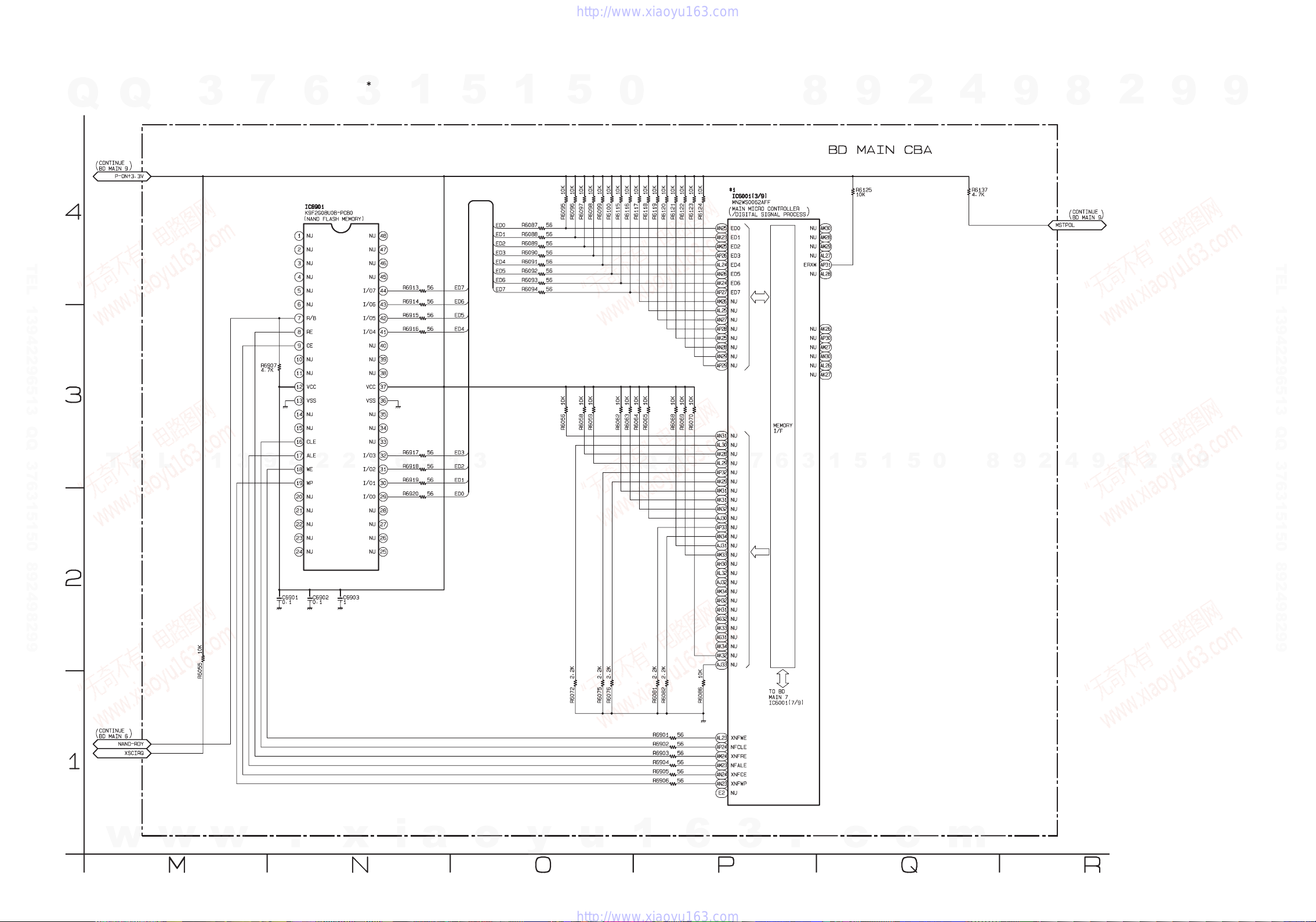
BD Main 3 Schematic Diagram
Q
Q
3
7
6
1 NOTE:
The order of pins shown in this diagram is different from that of actual IC6001.
3
1
IC6001 is divided into nine and shown as IC6001 (1/9) ~ IC6001 (9/9) in this BD Main Schematic Diagram Section.
5
1
5
0
8
9
2
4
9
8
2
9
9
TEL 13942296513 QQ 376315150 892498299
T
E
L
1
3
9
4
2
2
9
6
5
1
3
Q
Q
3
7
6
3
1
5
1
5
0
8
9
2
4
9
8
2
9
TEL 13942296513 QQ 376315150 892498299
9
w
w
w
.
x
i
a
o
y
u
1
1-10-13
6
3
.
c
o
m
E5SF0SCBD3
Page 43

BD Main 4 Schematic Diagram
Q
Q
3
7
6
1 NOTE:
The order of pins shown in this diagram is different from that of actual IC6001.
IC6001 is divided into nine and shown as IC6001 (1/9) ~ IC6001 (9/9) in this BD Main Schematic Diagram Section.
3
1
5
1
5
0
8
9
2
4
9
8
2
9
9
TEL 13942296513 QQ 376315150 892498299
T
E
L
1
3
9
4
2
2
9
6
5
1
3
Q
Q
3
7
6
3
1
5
1
5
0
8
9
2
4
9
8
2
9
TEL 13942296513 QQ 376315150 892498299
9
w
w
w
.
x
i
a
o
y
u
1
1-10-14
6
3
.
c
o
m
E5SF0SCBD4
Page 44

BD Main 5 Schematic Diagram
Q
TEL 13942296513 QQ 376315150 892498299
Q
3
7
6
1 NOTE:
The order of pins shown in this diagram is different from that of actual IC6001.
IC6001 is divided into nine and shown as IC6001 (1/9) ~ IC6001 (9/9) in this BD Main Schematic Diagram Section.
3
1
5
1
5
0
8
9
2
4
9
8
2
9
9
TEL 13942296513 QQ 376315150 892498299
T
E
L
1
3
9
4
2
2
9
6
5
1
3
Q
Q
3
7
6
3
1
5
1
5
0
8
9
2
4
9
8
2
9
9
w
w
w
.
x
i
a
o
y
u
1
1-10-15
6
3
.
c
o
m
E5SF0SCBD5
Page 45

BD Main 6 Schematic Diagram
Q
Q
3
7
6
1 NOTE:
The order of pins shown in this diagram is different from that of actual IC6001.
3
1
IC6001 is divided into nine and shown as IC6001 (1/9) ~ IC6001 (9/9) in this BD Main Schematic Diagram Section.
5
1
5
0
8
9
2
4
9
8
2
9
9
TEL 13942296513 QQ 376315150 892498299
T
E
L
1
3
9
4
2
2
9
6
5
1
3
Q
Q
3
7
6
3
1
5
1
5
0
8
9
2
4
9
8
2
9
TEL 13942296513 QQ 376315150 892498299
9
w
w
w
.
x
i
a
o
y
u
1
1-10-16
6
3
.
c
o
m
E5SF0SCBD6
Page 46

BD Main 7 Schematic Diagram
Q
Q
3
7
6
1 NOTE:
The order of pins shown in this diagram is different from that of actual IC6001.
3
1
IC6001 is divided into nine and shown as IC6001 (1/9) ~ IC6001 (9/9) in this BD Main Schematic Diagram Section.
5
1
5
0
8
9
2
4
9
8
2
9
9
TEL 13942296513 QQ 376315150 892498299
T
E
L
1
3
9
4
2
2
9
6
5
1
3
Q
Q
3
7
6
3
1
5
1
5
0
8
9
2
4
9
8
2
9
TEL 13942296513 QQ 376315150 892498299
9
w
w
w
.
x
i
a
o
y
u
1
1-10-17
6
3
.
c
o
m
E5SF0SCBD7
Page 47

BD Main 8 Schematic Diagram
Q
TEL 13942296513 QQ 376315150 892498299
Q
3
7
6
3
1
5
1
5
0
8
9
2
4
9
8
2
9
9
TEL 13942296513 QQ 376315150 892498299
T
E
L
1
3
9
4
2
2
9
6
5
1
3
Q
Q
3
7
6
3
1
5
1
5
0
8
9
2
4
9
8
2
9
9
w
w
w
.
x
i
a
o
y
u
1
1-10-18
6
3
.
c
o
m
E5SF0SCBD8
Page 48

BD Main 9 Schematic Diagram
Q
Q
3
7
6
1 NOTE:
The order of pins shown in this diagram is different from that of actual IC6001.
3
1
IC6001 is divided into nine and shown as IC6001 (1/9) ~ IC6001 (9/9) in this BD Main Schematic Diagram Section.
5
1
5
0
8
9
2
4
9
8
2
9
9
TEL 13942296513 QQ 376315150 892498299
T
E
L
1
3
9
4
2
2
9
6
5
1
3
Q
Q
3
7
6
3
1
5
1
5
0
8
9
2
4
9
8
2
9
TEL 13942296513 QQ 376315150 892498299
9
w
w
w
.
x
i
a
o
y
u
1
1-10-19
6
3
.
c
o
m
E5SF0SCBD9
Page 49

BD Main 10 Schematic Diagram
Q
TEL 13942296513 QQ 376315150 892498299
Q
3
7
6
3
1
5
1
5
0
8
9
2
4
9
8
2
9
9
TEL 13942296513 QQ 376315150 892498299
T
E
L
1
3
9
4
2
2
9
6
5
1
3
Q
Q
3
7
6
3
1
5
1
5
0
8
9
2
4
9
8
2
9
9
w
w
w
.
x
i
a
o
y
u
1
1-10-20
6
3
.
c
o
m
E5SF0SCBD10
Page 50

BD Main 11 Schematic Diagram
Q
Q
3
7
6
1 NOTE:
The order of pins shown in this diagram is different from that of actual IC6001.
3
1
IC6001 is divided into nine and shown as IC6001 (1/9) ~ IC6001 (9/9) in this BD Main Schematic Diagram Section.
5
1
5
0
8
9
2
4
9
8
2
9
9
TEL 13942296513 QQ 376315150 892498299
T
E
L
1
3
9
4
2
2
9
6
5
1
3
Q
Q
3
7
6
3
1
5
1
5
0
8
9
2
4
9
8
2
9
TEL 13942296513 QQ 376315150 892498299
9
w
w
w
.
x
i
a
o
y
u
1
1-10-21
6
3
.
c
o
m
E5SF0SCBD11
Page 51

BD Main 12 Schematic Diagram
Q
Q
3
7
6
3
2 NOTE:
The order of pins shown in this diagram is different from that of actual IC8001.
1
IC8001 is divided into nine and shown as IC8001 (1/2) ~ IC8001 (2/2) in this BD Main Schematic Diagram Section.
5
1
5
0
8
9
2
4
9
8
2
9
9
TEL 13942296513 QQ 376315150 892498299
T
E
L
1
3
9
4
2
2
9
6
5
1
3
Q
Q
3
7
6
3
1
5
1
5
0
8
9
2
4
9
8
2
9
TEL 13942296513 QQ 376315150 892498299
9
w
w
w
.
x
i
a
o
y
u
1
1-10-22
6
3
.
c
o
m
E5SF0SCBD12
Page 52

BD Main 13 Schematic Diagram
Q
Q
3
7
6
3
2 NOTE:
The order of pins shown in this diagram is different from that of actual IC8001.
1
IC8001 is divided into nine and shown as IC8001 (1/2) ~ IC8001 (2/2) in this BD Main Schematic Diagram Section.
5
1
5
0
8
9
2
4
9
8
2
9
9
TEL 13942296513 QQ 376315150 892498299
T
E
L
1
3
9
4
2
2
9
6
5
1
3
Q
Q
3
7
6
3
1
5
1
5
0
8
9
2
4
9
8
2
9
TEL 13942296513 QQ 376315150 892498299
9
w
w
w
.
x
i
a
o
y
u
1
1-10-23
6
3
.
c
o
m
E5SF0SCBD13
Page 53

Audio CBA, Video CBA, Front-A CBA & Front-B CBA Top View
Q
Q
3
7
6
3
1
Front-A CBA
G
D3005
TEL 13942296513 QQ 376315150 892498299
SW3003
SW3008
BE5SE0F0101
D3001
D3002
RED
3 C
D3006
V-7
J3009
EV+3V3
2
003WS1003WS
C3007
J3008
FL+
J3007
J3003
LED5
J3011
REMOCON
D3004
J3010
EV+5V
EV+3V3
EV+5V
J3002
5
SW3004
SW3006
SW3007
J3001
1
5
0
BE5SE0F01013
J3012
DGND
L3001
J3005
J3004
REMOCON-VCC
SW3005
AD-KEY2-B
RS3001
DGND
J3014
C3001
Front-B CBA
SW3113
SW3118
SW3117SW3116
SW3108
FL3001
8
C3006
SW3119
9
SW3112
SW3106
CN3001
3
1
4
9
SW3110
SW3102
V-7
2
SW3111
SW3115SW3114
SW3104
DIP
1
234
8
G
SW3101
3 D
BE5SE0F0101
5
2
1
SW3109
CN3101
3
SW3107
7
SW3103
SW3105
9
9
TEL 13942296513 QQ 376315150 892498299
T
E
L
J2141
1
JK2201
JK2200
LFCLS
FR
JK2202BSL
SubSR
BSR
JK2203
3
C2212
C2211
9
C2816
C2815
C2828
C2827
C2840
C2839
C2853
C2852
4
2
2
C2204
IC2200
C2807
IC2601
3082C2082CC2804
IC2602
IC2603
IC2604
J2140
J2139
8312J7312J6312J
9
6
C2205
C2806
C2855
7582C6582C
5
C2822
C2821
C2834
C2847
C2846
C2208
C2207
C2810
C2809
C2833
1
C2283
AUDIO+5V
J2135
AUDIO+5V
ZSW
AUDIO+5V
ZFL3
J2132
J2133
AUDIO+5V
AUDIO+12V5
J2128
J2129
AUDIO+12V5
AUDIO+5V
J2126
J2127
3
J2118
J2116
J2115
26
J2134
AUDIO+12V5
19
AUDIO+12V5
J2130
J2131
J2106
J2105
J2104
J2103
J2102
J2101
J2121
L2202
ZFL3
ZSW
ZLFE
ZLFE
AUDIO+12V5
J2114
J2113
J2112
J2111
J2110
J2142
J2109
CN2007
J2108
J2107
1
JP2085
J2082
JP2081
J2080
JP2079
ZFL1
ZFR1
ZFR3
ZFL3
ZSW
GND
ZC
ZSSR
ZBS
GND
C2281
AG
AG
J2124
C2285
JP2122
J2119
J2117
Q2280
D2280
C2282
EV+3V3
AG
D2281
PON+12V5
JP2120
AG
D2282
R2326
R2622
D2625
J2123
J2075
JP2074
Q2636
JP2125
SAFTY2
L2306
VID+5V
GNDA
J2073
J2072
J2071
J2068
J2067
R2278
R2279
D2648
J2043
16
R2327
J2061
J2059
L2607
GNDA
Q2302
D2301
C2301
C2220
C2651
Q
MAIN-PON
FAN-LOCK
EV+3V3
PWSW2
FAN-CONT1
GNDA
GNDA
IC2002
GNDA
Q
SAFTY2
PWSW3
JP2011
J2078
J2065
J2064
J2063
232C-PW-CONT
J2062
JP2060
GNDA
JP2048
JP2046
J2044
GNDA
J2042
JP2070
GNDA
PWSW1
J2077
J2076
J2069
REMOTE
J2066
CEC+3V9
SYS-RESET
RDY
GNDA
J2047
J2045
GNDA
GNDA
J2041
CN2008
GNDD
/MUTE2
J2056
GNDD
EV+3V3
/AMUTE
CN2003
1
3
+FL
J2053
/MUTE1
SD/HD
J2055
JP2030
J2021
F2-IN
J2052
GNDA
J2054
D2624
C2016
GNDD
F1-IN
J2051
EV+5V
J2049
C2637
MODE
6
J2023
1
7
EV+5V
J2050
CEC-IN
J2037
X2000
J2083
J2040
J2039
CEC-OUT
232C-RXD
J2036
J2035
EV+3V3
J2022
D2640
6
1
EV+5V
232C-TXD
J2034
JP2029
FL-CLK
GNDD
JP2033
J2027
JP2028
FL-RST
FL-DAT
3
J2038
GNDD
J2032
J2026
FL-STB
J2007
GNDD
IC2000
R2602
D2601
EV+5V
JP2004
1
VID+5V
GNDD
Q2602
EV+3V3
REMOTE
J2008
J2084
R2601
JP2020
Q2604
D2602
J2018
JP2017
J2016
J2015
J2014
SUB-RXD
J2002
J2003
21
5
CN2005
FL+
R2608
Q2601
GNDA
J2013
J2012
J2011
J2010
J2009
GNDD
SW2001
SAFTY2
SUB-TXD
JP2006
JP2012
SAFTY2
1
SAFTY2
R2615
R2616
GNDD
J2081
27
D2603
R2617
R2618
F2-IN
J2019
CN2002
21
LINE3
LINE2
LINE1
DET
SAFTY1
JP2005
J2001
EV+3V3
0
5
D2604
R2619
1
17
3 A
BE5SE0F0101
V-7
AB
8
CVBS
J4006
JK4001
J4007
Y
JK4002
J4032
Cb
JK4003
Cr
JK4004
C4014
L4003
JK4000
COAXIAL
JP4001
SPDIF
JK4005
OPTICAL
9
1
J4008
Pr-D
J4029
C4021
J4015
C4013
JP4022
2
Pb-D
PY-D
Pr-D
C4012
C4016
VG
C4019
J4028
DIGITAL+5V
C4023
C4011
C4005
J4030
C4010
4
GND
J4021
C4301
D4301
18
IC4000
J4018
D4282
L4001
8
9
V-7
BE5SE0F0101
CN4002CN4000
16
Pb-D
J4002
PY-D
J4003
Pr-D
J4004
J4005
L4000
C4006
L4306
C4008
J4014
GNDD
GND
J4031
Q4000
Q4302
F
VG
J4013
J4012
REMOTE
J4020
JP4019
J4026
VIDEO+5V
R4326
R4327
P
b
J4011
J4010
EV+5V
232C-PW-CONT
EV+3V3
J4017
J4023
EV+3V3
J4025
J4027
EV+3V3
2
3 B
J4009
232C-TXD
232C-RXD
GNDD
J4016
GNDD
VIDEO+5VVIDEO+5V
CN4001
J4024
Q4002Q4001
G
9
CN4003
1
27
9
1
10
w
w
Audio CBA
w
.
x
i
a
o
y
u
1
6
1-10-24
3
.
c
o
m
Video CBA
BE5SE0F01013
Page 54

Audio CBA, Video CBA, Front-A CBA & Front-B CBA Bottom View
Q
Q
3
7
6
3
1
Front-B CBA
SW3109
R3125
SW3110
G
SW3102
R3115
R3114
1
3
TEL 13942296513 QQ 376315150 892498299
CN3101
7
SW3107
SW3103
SW3105
R3120
SW3114
SW3101
R3121
R3113
CN3001
3
1
R3117
SW3111
DIP
5
1234
C3009
R3032
SW3115
SW3104
C3006
R3034
C3005
C3008
5
R3118
R3119
R3123
R3031
SW3112
R3030
R3124
SW3106
1
SW3119
R3116
SW3118
R3122
FL3001
5
SW3113
SW3117 SW3116
SW3108
0
R3035
R3036
C3002
DGND
C3001
RS3001
J3014
R3027
C3003
SW3005
C3004
R3028
8
Front-A CBA
SW3004
Q3003
SW3006
DGND
SW3007
R3025
R3023
R3024
AD-KEY2-B
REMOCON-VCC
L3001
L3002
R3029
9
D3004
EV+5V
Q3004
Q3005
LED5
EV+3V3
R3008
R3007
R3009
EV+5V
2
D3005
REMOCON
1
R3033
FL+
4
CN3002
C3007
17
18
EV+3V3
9
21
D3006
R3026
R3006
R3004
R3005
R3003
SW3002
8
Q3002
Q3001
2
G
SW3003
R3002
R3001
SW3001
D3001
D3002
SW3008
9
9
TEL 13942296513 QQ 376315150 892498299
T
E
R4035
Q4002
5
21
R4037
R4039
VIDEO+5V
R4033
R4036
R4042
R4326
R4327
L
C4000
C4404
R4031
Q4001
R4034
R4406
1
R4405
CN4003
10
C4402
1
EV+3V3
232C-PW-CONT
232C-RXD
232C-TXD
GNDD
CN4001
27
VIDEO+5V
R4040
R4032
CN4002
R4027
EV+3V3
GNDD
R4028
R4029
R4030
PY-D
Pr-D
Pb-D
VG
EV+5V
R4057
VIDEO+5V
1
16
REMOTE
R4011
R4012
R4026
R4041
R4007
GNDD
R4023
R4025
R4021
D4282
Q4000
R4024
C4401
R4006
C4004
GND
R4058
L4306
Q4302
R4401
3
R4002
R4004
R4020
C4006
L4000
C4301
C4403
C4015
L4001
18
R4005
R4017
C4003
R4402
R4001
R4003
R4019
C4007
C4008
R4403
R4000
D4301
9
C4002
C4005
IC4000
C4016
L4002
C4010
C4009
R4043
C4017
R4328
R4329
CN4000
R4016
R4015
R4049
R4022
R4018
C4001
GND
C4019
R4038
4
C4011
R4056
C4024
C4020
PY-D
Pr-D
Pb-D
C4012
R4045
R4010
R4047
C4014
VG
C4022
C4013
L4003
R4048
2
1
R4046
Q4003
SPDIF
C4023
R4404
R4052
R4053
Pr-D
C4021
R4051
OPTICAL
R4055
C4026
C4018
R4050
JK4005
C4025
R4044
C4027
R4054
2
9
JK4001
CVBS
Y
JK4002
Q4004
JK4003
Cb
JK4004
Cr
COAXIAL
JK4000
6
5
R2036
R2051
R2052
R2049
JC2002
R2071
C2014
C2015
R2072
D2604
R2619
CN2002
R2039
R2045
27
D2603
R2618
1
LINE3
LINE2
LINE1
DET
SAFTY1
R2061
R2059
EV+3V3
R2004
SAFTY2
1
R2608
R2617
R2616
Q2604
F2-IN
21
SW2001
R2047
SAFTY1
R2037
R2607
R2615
SAFTY2
3
Q2601
GNDA
GNDD
EV+5V
EV+3V3
GNDD
R2999
R2012
R2601
REMOTE
R2017
R2018
39
R2006
R2604
D2602
R2015
C2065
R2009
R2011
SUB-TXD
SUB-RXD
R2007
R2605
R2010
IC2000
R2050
CN2005
GNDD
Q2602
Q2002
R2020
27
52
R2035
R2602
Q2603
R2031
R2058
D2601
JC2001
R2032
26
1
R2055
R2033
R2057
VID+5V
GNDD
R2603
FL-STB
GNDD
R2034
R2001
R2063
R2073
C2007
R2056
GNDD
FL-RST
R2023
13
1
EV+5V
FL-DAT
R2013
R2076
R2016
R2014
R2024
232C-TXD
FL-CLK
Q2637
Q2638
R2025
R2026
CEC-OUT
232C-RXD
Q2614
C2637
C2005
X2000
EV+3V3
D2640
CEC-IN
R2000
R2002
R2074
R2075
C2008
MODE
1
EV+5V
EV+5V
F1-IN
R2665
R2003
R2666
C2006
GNDD
CN2003
F2-IN
GNDA
EV+3V3
C2016
+FL
SD/HD
D2624
C2009
R2029
CN2008
/MUTE2
/MUTE1
R2053
1
CEC+3V9
GNDD
GNDA
/AMUTE
R2027
Q
GNDD
REMOTE
GNDA
GNDA
NRST
GNDA
PWSW1
PWSW2
FAN-CONT1
SYS-RESET
RDY
232C-PW-CONT
Q2302
D2301
C2301
R2661
C2626
C2651
Q
PWSW3
SAFTY2
R2328
C2650
GNDA
MAIN-PON
FAN-LOCK
EV+3V3
C2220
C2649
GNDA
16
R2278
R2279
GNDA
GNDA
R2329
GNDA
SAFTY1
L2306
VID+5V
GNDA
IC2002
L2607
R2625
R2623
3
D2282
R2326
Q2280
D2280
C2282
R2660
R2624
R2284
GNDA
D2648
Q2636
PON+12V5
R2327
D2281
GND
R2280
7
R2939
R2940
ZSSR
R2621
C2627
D2625
ZFR3
ZFL3
ZBS
AG
ZFL1
ZFR1
ZSW
ZC
R2973
R2957
R2971
R2974
R2958
R2972
R2977
R2980
R2979
R2229
R2220
R2223
R2943
R2944
R2945
R2281
R2622
6
AG
R2224
R2221
R2230
R2918
R2919
R2916
R2917
R2911
C2281
EV+3V3
C2286
R2206
C2280
3
Q2629
R2912
R2913
Q2630
R2914
Q2633
R2915
C2285
Q2200
AG
AG
Q2201
Q2623
Q2622
R2910
Q2626
1
AUDIO+12V5
L2202
R2207
1
ZFL3
ZSW
ZLFE
ZLFE
5
C2284
AUDIO+5V
26
C2283
AUDIO+12V5
CN2007
AUDIO+12V5
1
AUDIO+5V
AUDIO+5V
ZFL3
AUDIO+12V5
AUDIO+5V
AUDIO+12V5
AUDIO+5V
R2211
C2206
C2805
C2820
R2960
C2832
R2982
C2845
R2922
R2947
4
R2210
4
R2921
4
R2946
4
R2959
4
R2981
8
R2213
C2216
IC2200
1
8
C2215
R2212
R2924
C2814
IC2601
1
8
C2813
R2923
R2926
C2826
IC2602
1
8
C2825
R2925
R2928
C2838
IC2603
1
8
C2837
R2927
R2930
C2851
IC2604
1
8
C2850
R2929
C2213
C2808
C2819
C2831
C2843
9
C2204
C2807
C2803
C2804
C2802
2
C2816
C2815
C2828
C2827
C2840
C2839
C2853
C2852
C2212
C2211
4
R2215
R2226
R2938
R2933
R2937
R2956
R2953
R2952
R2942
R2970
R2966
R2965
R2969
R2976
R2978
R2987
R2214
R2216
R2934
R2932
R2931
R2951
R2950
R2975
C2208
R2217
C2207
C2810
R2941
C2809
C2822
ZSW
R2992
C2821
C2834
R2994
C2833
C2847
R2993
C2846
C2210
C2209
R2208
R2903
C2812
C2811
R2920
R2905
C2824
C2823
R2904
R2907
C2836
C2835
R2906
R2909
C2849
C2848
R2908
C2205
C2806
C2855
C2857
C2856
R2209
0
5
R2964
R2963
R2986
R2985
R2219
9
R2218
C2818
C2817
C2830
C2829
C2217
C2214
Q2625
Q2624
Q2628
Q2627
C2841C2842
C2844
Q2635
Q2634
C2854
Q2202
Q2203
Q2632
Q2631
AG
8
R2228
R2935
R2954
R2967R2968
R2227
R2955
R2989
R2988
R2936
C2219
2
C2218
JK2202
JK2203
JK2201
9
9
w
Video CBA
w
w
.
x
i
a
Audio CBA
o
y
u
1
6
1-10-25
3
.
c
o
m
BE5SE0F01013
Page 55

Power Supply CBA, SD CBA & RS232C CBA Top View
Because a hot chassis ground is present in the power supply
circuit, an isolation transformer must be used when repairing.
Also, in order to have the ability to increase the input slowly,
when troubleshooting this type of power supply circuit,
a variable isolation transformer is required.
CAUTION !
Q
Fixed voltage (or Auto voltage selectable) power supply circuit is used in this unit.
If Main Fuse (F1001) is blown , check to see that all components in the power supply
Q
circuit are not defective before you connect the AC plug to the AC power supply.
Otherwise it may cause some components in the power supply circuit to fail.
3
7
6
3
1
5
1
A V
CAUTION !
F
For continued protection against fire hazard,
replace only with the same type fuse.
5
ATTENTION : Pour une protection continue les risqes
d'Incele n'utiliser que des fusible de même type.
Risk of fire-replace fuse as marked.
0
"This symbol means fast operating fuse."
"Ce symbole reprèsente un fusible à fusion rapide."
8
9
2
NOTE:
The voltage for parts in hot circuit is measured using
hot GND as a common terminal.
4
9
8
2
9
9
SD CBA RS232C CBA
TEL 13942296513 QQ 376315150 892498299
b
P
CN5000
3 B
BE5SE0F0102
Power Supply
CBA
b
T
E
L
w
w
P
1
J1149
PON+5V1
D1107
D1108
BE5SE0F0102
J1124
3 A
V-1
GNDA
w
G
3
C1205
GNDA
L1101
J1122
GNDA
J1138
R1208
9
C1203
C1102
J1143
GNDA
R1133
SAFTY2
C1104
D1120
R1122
Q1120
R1132
R1124
R1127
J1154
C1051
4
GNDA
J1123
Q1201
C1120
R1125
R1128
D1121
.
D1204
D1205
2
D1203
D1202
GNDA
J1142
L1401
J1147
FAN_LOCKA
C1710
Q1202
2
D1201
R1205
D1105
IC1401
J1117
GNDA
J1162
C1049
x
24
R1204
Q1203
D1101
+5V
PON+1V2
J1130
+5V
9
J1113
Q1108
D1R2V_GND
J1141
C
G
CN5001
V-1
C1201
6
GNDA
J1115
+5V
J1114
R1113
PG
L1451
J1145
PON+1V8
D1R8V_GND
C1050
J1144
i
30
0
1
N
Not Used
115
Z1002
L1201
GNDA
J1121
5
1
C1202
L1202
D1102
R1112
D1103
J1136
C1401
Q1106
F1_IN
F2_IN
J1131
+5V
+5V
J1132
J1134
J1133
C1451
IC1451
CN1005
12
PON+10V5
C1052
a
1
PG
R1106
C1032
J1139
J1116
C1048
J1146
J1148
PON+5V1
J1111
3
PG
L1305
+5V
1
o
BE5SE0F0102
G
L1004
C1031
C1101
+5V
J1126
R1136
SAFTY2
J1156
PON+12V5
J1125
CN1002
PG
J1112
F1_IN
F2_IN
J1135
J1137
y
3 D
R1035
IC1301
CN1004
Not Used
Z1001
AC1001
P
b
COLD
J1108
PG
1
Q
Q
D1036
D1032
C1024
D1509
D1513
L1501
D1511
C1509
2
C1026
D1028
C1303
J1151
PON+3V3
Photo_k
J1110
C1301
J1368
+5V
D1302
u
+5V
J1109
C1030
GNDA
J1153
C1029
D1034
D1033
D1031
D1030
PG
J1127
J1155
PG2
FL
J1129
D1035
D1027
D1301
C1033
C1705
EV+5V
J1128
16
1
1-10-26
1
PG2
2
IC1502
J1507
D1510
6
4
3
IC1004
T1001
3
C1016
C1015
T1501
D1018
D1020
SUB_PWR
7
J1152
4
3
3
C1018
C1022
D1508
R1503
6
FET_SW
IS
J1105
D1023
D1507
D1506
R1504
J1104
C1023
D1022
IC1501
C1504
.
IC1002
3
D1009
Q1002
R1024
D1505
R1505
Q1001
1
D1021
D1025
J1502
C1501
R1025
D1502
FG2
5
PWR
J1103
D1504
D1501
c
D1013
D1503
16
1
R1013
15
C
101
9
C1013
2
C150
o
5
D1011
D1012
J1101
CN1100
JK5550
3 C
V-1
BE5SE0F0102
CN5501
1
B3.5-AVbox AV-JIG ver.3
CN5500
D5501
Q5552
Q5500
R5504
Q5551
IC5550
C5553
GND
6
J5503
HOT
RISK OF FIRE-REPLACE
0
D1010
C1010
RL1501
D1512
1
8
J1161
FUSE AS MARKED
9
J1364
2
C1009
J1163
1
15
4
L1001
L1002
CN1101
m
D5500
C5505
IC5500
AV-RS232C-PCB
Q5501
SA1001
J5501
RS232C-BLOCK
8
9
C1003
F1001
T2.5A H250V
FH1001
ver.2
D5502
D5503
b
P
J5502
R1001
2
CN1001
C5506
G
9
9
2
1
FH1002
Not Used
CN6
B3.5-AVbox PW-JIG
BE5SE0F01023
TEL 13942296513 QQ 376315150 892498299
B3.5C
Page 56

Power Supply CBA, SD CBA & RS232C CBA Bottom View
Because a hot chassis ground is present in the power supply
circuit, an isolation transformer must be used when repairing.
Also, in order to have the ability to increase the input slowly,
when troubleshooting this type of power supply circuit,
a variable isolation transformer is required.
CAUTION !
Q
Fixed voltage (or Auto voltage selectable) power supply circuit is used in this unit.
Q
If Main Fuse (F1001) is blown , check to see that all components in the power supply
circuit are not defective before you connect the AC plug to the AC power supply.
Otherwise it may cause some components in the power supply circuit to fail.
3
7
6
3
1
5
1
A V
CAUTION !
F
For continued protection against fire hazard,
replace only with the same type fuse.
5
ATTENTION : Pour une protection continue les risqes
d'Incele n'utiliser que des fusible de même type.
Risk of fire-replace fuse as marked.
0
"This symbol means fast operating fuse."
"Ce symbole reprèsente un fusible à fusion rapide."
8
9
2
NOTE:
The voltage for parts in hot circuit is measured using
hot GND as a common terminal.
4
9
8
2
9
9
RS232C CBA
D5501
Q5500
C5507
R5553
C5553
R5558
Q5552
R5551
JK5550
C5551
R5555
C5552
1
Q5551
4
R5552
C5550
GND
D5500
L5501
L5500
R5504
IC5500
R5500
16
R5502
9
1
R5501
Q5501
R5503
6
5
CN5500
C5502
C5504
D5502
D5503
C5505
8
9
C5506
C5503
C5501
1
C5500
TEL 13942296513 QQ 376315150 892498299
Power Supply
T
E
CBA
L
1
3
9
4
2
2
9
Not Used
B3.5-AVbox
1
1
24
B3.5C
CN6
1
w
w
29
w
2
30
30
ver.2
B3.5-AVbox PW-JIG
.
RL1501
R5000
1
CN1101
15
x
6
D1512
IC5550
CN5501
6
i
R5554
1
Not Used
5
1
C1010
1
CN11
a
11126618
CN2
B3.5
B3.5-AVbox
CN1
CN3
HT2
B3.5-AVbox AV-JIG ver.3
8
IC1002
1
C1006
R1502
C1505
5
FET_SW
4
D1018
R1021
5
4
IS
C1507
C1012
R1003
C1016
C1506
1
SUB_PWR
R1019
Q
C1015
IC1502
4
R1506
3
J1106
1-10-27
3
C1013
00
o
R1017
R1016
R1012
R1011
PWR
15
16
y
R1010
C1503
FG2
R1018
R1009
C1004
R1022
R1023
R1501
1
8
u
R1
D1020
Q
T1501
R1513
4
3
T1001
R1507
R1508
1
2
R1514
Q1501
CN4
IC1004
C1025
R1510
D1509
PG2
6
B3.5C
1
D1036
2
D1032
C1024
D1513
D1510
R1032
3
R1034
C1508
R1509
D1511
R1031
D1035
A
R1033
D1034
D1033
D1031
D1030
C1034
R1512
C1705
L1501
3
PG
7
A
A
A
A
C1033
R1304
R1511
C1509
Not Used
+5V
C1029
3
6
K
D1027
C1301
PG
R1302
D1301
R1305
R1303
Q1301
PG2
EV+5V
C1304
R1306
R1307
GNDA
FL
16
.
Photo_K
C1026
R1036
C1028
K
K
K
K
R1301
C1302
D1302
1
R1037
IC1301
+5V
R1040
R1039
R1038
C1303
R1137
PON+3V3
CN1004
c
D1028
C1030
R1035
5
R1138
R1135
F2_IN
PG
Q1109
F1_IN
L1004
1
+5V
Q1110
C1031
C1101
L1305
SAFTY2
PON+12V5
o
PG
R1107
C1032
R1136
1
5
PON+5V1
0
Q1103
PG
C1451
C1457
C1455
+5V
C1456
C1454
C1048
L1201
C1202
R1106
Q1106
F1_IN
F2_IN
R1452
5
1
C1452
C1453
PON+10V5
m
1
SD CBA
C5006
1
C5007
15
GNDA
C1201
R1201
8
L1202
R1103
D1102
R1112
D1103
+5V
8
IC1451
4
D1451
CN1005
C1052
K
+5V
A
C1458
C1459
2
1
R1455
+5V
C1461
L1451
D1R8V_GND
C
N
R1108
GNDA
Q1104
R1113
C1406
C1404
PG
R1454
C1050
01
CN5001
R1203
9
R1453
PON+1V8
30
+5V
3021Q2021Q
D1101
C1405
C1401
C1403
C1402
+5V
D1R2V_GND
C1122
C5006
8
9
R1204
2
D1201
R1205
Q1108
R1401
8
1
C1408
PON+1V2
10
D1204
D1105
C1407
R1451
24
1
D1205
5
4
K
C1121
GNDA
C1049
7
R5007
R5005
R5008
L5002
CN5000
R5009
R5003
R5010
R5002
R5011
R5001
4
D1203
D1202
GNDA
R1117
R1403
IC1401
C1710
R1130
R5006
L5001
C5001
C5002
C5003
Q1204
R1206
R1207
R1118
R1404
A
D1401
L1401
R1402
FAN_LOCKA
11
R5004
C5008
C5004
Q1205
9
Q1201
C1120
R1122
R1125
R1128
R1129
C1051
R1208
GNDA
R1120
Q1120
R1132
D1121
R1202
C1104
R1123
R1131
R1209
C1204
8
C1102
GNDA
D1120
R1124
R1127
C1203
R1104
R1121
R1133
R1126
2
PON+5V1
C1205
L1101
GNDA
Q1122
R1134
Q1121
SAFTY2
9
9
D1107
D1108
GNDA
GNDA
BE5SE0F01023
TEL 13942296513 QQ 376315150 892498299
Page 57

Q
Q
Cabinet
3
2L082
7
6
3
1
5
1
2L082
EXPLODED VIEWS
5
0
B71
B70
2L034
2L056
8
Video CBA
9
2
4
9
See Electrical Parts List
for parts with this mark.
Some Ref. Numbers are
not in sequence.
8
2
9
9
TEL 13942296513 QQ 376315150 892498299
A3
A26
T
E
L
A14
1
3
9
4
A26
2
2
A26
9
Audio CBA
6
5
1
2L082
3
2L032
2L082
W005
W009
2L040
A'
2L028
2L040
B72
2L054
Q
Q
W003
SD CBA
2L051
2L057
B73
2L054
3
W002
7
2L049
2L028
BD Main CBA &
BD Mechanism
Assembly
2L058
A
2L015
3
6
F1001
RS232C CBA
2L027
W001
5
1
Power Supply CBA
B74
2L026
1
2L058
FM1001
5
A4
0
2L070
W004
8
2L061
9
2L081
2L070
2
2L081
2L083
2L081
A20-3
4
9
2L073
A30
2L063
8
2
9
TEL 13942296513 QQ 376315150 892498299
9
w
w
w
2L064
A8
.
Front-A CBA
x
2L064
A1X
2L018
i
A7
B2
2L036
a
2L036
2L064
2L018
o
2L018
Front-B CBA
y
A6
2L036
2L036
u
c
B39
o
m
B4
2L040
A2
6
2L040
3
A6
.
A6
1
1-11-1 E5SF0CEX
Page 58

Q
Packing
Lower Side Upper Side
Q
3
7
6
3
1
5
1
5
0
8
9
2
4
9
8
2
9
9
X6
TEL 13942296513 QQ 376315150 892498299
S1
TEL
13942296513
X14
S3
X46
Q
Q
3
7
S8
6
3
1
X15
X19
5
1
5
0
X10
8
X1X40X34
9
2
4
9
8
2
9
TEL 13942296513 QQ 376315150 892498299
9
w
w
A20-1
w
S2
.
xia
FRONT
o
y
S1
A20-2
u
1
6
3
.
c
o
1-11-2 E5SF1PEX
Some Ref. Numbers
are not in sequence.
m
Page 59

MECHANICAL PARTS LIST
PRODUCT SAFETY NOTE: Products marked with a
Q
Q
# have special characteristics important to safety.
Before replacing any of these components, read
carefully the product safety notice in this service
manual. Don't degrade the safety of the product
through improper servicing.
NOTE: Parts that are not assigned part numbers
(---------) are not available.
TEL 13942296513 QQ 376315150 892498299
Ref. No. Description Part No.
A1X FRONT ASSEMBLY E5SF0UD 1VM021932
A2 CHASSIS E5KA0UD 1VM021192J
A3 TOP COVER E5KA0UD 1VM021193
A4 REAR PANEL E5SF0UD 1VM229777
A6 FOOT ASSEMBLY E5KE0UD 1VM433859
A8 TRAY PANEL ASSEMBLY E5SF0UD 1VM229917
A14 TOP PLATE E5KE0UD 1VM228897
A20-1 BAR CODE LABEL E5SF0UD ---------A20-2 BAR CODE LABEL E5SF0UD ---------A20-3 BAR CODE LABEL E5SF0UD ---------A26 DOUBLE SIDE TAPE E5KA0UD 1VM329678
A30 MODEL NO. LABEL E5SF1UD ---------2L015 SCREW TAP TIGHT WASHER+ P-TIGHT GCJP3080
2L018 SCREW P-TIGHT M3X8 BIND HEAD+ GBJP3080
2L026 SCREW S-TIGHT M3X6 E5E10UD 1VM429667
2L027 SCREW S-TIGHT M3X6 E5E10UD 1VM429667
TEL
2L028 SCREW S-TIGHT M3X10 BIND HEAD+ GBJS3100
2L032 SCREW S-TIGHT M3X6 E5E10UD 1VM429667
2L034 SCREW S-TIGHT M3X6 E5E10UD 1VM429667
2L036 SCREW S-TIGHT M3X6 BIND HEAD+ GBJS3060
2L040 SCREW P-TIGHT M3X8 BIND HEAD+ GBJP3080
2L049 SCREW S-TIGHT M3X6 E5E10UD 1VM429667
2L051 SCREW TAP TIGHT WASHER+ P-TIGHT GCJP3080
2L054 SCREW C-TIGHT M3X6 E5610UD 0VM412937A
2L056 SCREW S-TIGHT M3X6 BIND HEAD+ GBJS3060
2L057 SCREW S-TIGHT M3X6 BIND HEAD+ GBJS3060
2L061 HEXAGON SPACER E6AE0UD 1VM424730
2L063 SCREW S-TIGHT M3X8 DISH HEAD+ GDHS3080
2L064 SCREW S-TIGHT M3X8 DISH HEAD+ GDHS3080
2L070 B-TIGHT SCREW M3X8 E5E00UD 1VM428563
2L073 B-TIGHT SCREW M3X8 E5E00UD 1VM428563
2L081 S-TIGHT SCREW M3X6 E5E00UD 1VM428564
2L082 S-TIGHT SCREW M3X6 E5E00UD 1VM428564
2L083 S-TIGHT SCREW M3X6 E5E00UD 1VM428564
B2 FRONT BRACKET E5SE0UD 1VM332919
B4 POWER HOLDER E5KA0UD 1VM122880
B39 LEAD CLAMPER 100MM 1790356
B70 HIMELON TAPE(5X40) E5KA0UD 1VM431686
B71 HIMELON TAPE(5X25) E5KA0UD 1VM431688
B72 AV PCB BRACKET E5SE0UD 1VM229337
B73 LOADER BRACKET E5SE0UD 1VM124559
FM1001# MOTOR DC FAN 2D65BL100190 MMEZR12XNR08
W001 WIRE ASSEMBLY FFC 24/60/1.0 WX1E5SF1-002
W002 WIRE ASSEMBLY FFC 15/65/1.0 WX1E5SF1-003
W003 WIRE ASSEMBLY FFC 15/105/1.0 WX1E5SF1-004
w
w
W004# WIRE ASSEMBLY AC INLET 2/300/AWG20 WX1E5SF1-005
W005 WIRE ASSEMBLY FFC 26/169/1.0 WX1E5KA0-006
3
7
6
3
1
13942296513
w
.
xia
5
o
1
y
5
u
0
Q
Ref. No. Description Part No.
W009 WIRE ASSEMBLY PH 16/290/AWG24 WX1E5KA0-010
S1 SIDE PAD E5SF0UD 1VM124879
S2 GIFT BOX CARTON E5SF0UD 1VM334418
S3 SET BAG E5KB0UD 1VM433842B
S8 PARTITION PAD E5SE0UD 1VM435619
X1# OWNERS MANUAL E5SF0UD 1VMN29853
X6 MANGANESE DRY BATTERY R6UWC/2STA XB0M311MS003
X10 ACCESSORY BAG E5795ED 0VM416059
X14 AV CORD 1000/BLACK WPZ0102TM018
X15# AC CORD W/O A GND WIRE UL/CSA/202/NO/
X19 REMOTE CONTROL UNIT NC116UD NC116UD
X34 NETFLIX GUIDE E5SF1UD 1VMN29733
X40 WARRANTY CARD E5H55UD 1VMN26326
X46 ACCESSORY BAG E5795ED 0VM416059
7
3
Q
1
6
3
8
BLACK
3
6
.
9
1
5
c
4
2
PACKING
ACCESSORIES
0
5
1
o
m
9
8
9
8
WAV0202LTE01
4
2
2
9
8
9
2
9
9
TEL 13942296513 QQ 376315150 892498299
9
20100721 1-12-1 E5SF0CA
Page 60

ELECTRICAL PARTS LIST
PRODUCT SAFETY NOTE: Products marked with a
Q
Q
# have special characteristics important to safety.
Before replacing any of these components, read
carefully the product safety notice in this service
manual. Don't degrade the safety of the product
through improper servicing.
NOTES:
1. Parts that are not assigned part numbers (---------)
are not available.
2. Tolerance of Capacitors and Resistors are noted
with the following symbols.
TEL 13942296513 QQ 376315150 892498299
C.....±0.25% D.....±0.5% F.....±1%
G.....±2% J......±5% K.....±10%
M.....±20% N.....±30% Z.....+80/-20%
BD MAIN CBA & BD MECHANISM
ASSEMBLY
Ref. No. Description Part No.
1B1 BD MAIN CBA & BD MECHANISM ASSEMBLY N7JR4CUN
AV ASSEMBLY
Ref. No. Description Part No.
TEL
VIDEO CBA
Ref. No. Description Part No.
C4001 CHIP CERAMIC CAP.(1608) B K 0.1µF/50V CHD1JK30B104
C4002 CHIP CERAMIC CAP.(1608) B K 0.1µF/50V CHD1JK30B104
C4003 CHIP CERAMIC CAP.(1608) B K 1µF/10V CHD1AK30B105
C4004 CHIP CERAMIC CAP.(1608) B K 1µF/10V CHD1AK30B105
C4005 ELECTROLYTIC CAP. 10µF/16V/M CEC10RENW016
C4006 ELECTROLYTIC CAP. 100µF/6.3V/M CEA101ENW016
C4007 CHIP CERAMIC CAP.(1608) F Z 0.1µF/50V CHD1JZ30F104
C4008 ELECTROLYTIC CAP. 220µF/6.3V/M CEA221ENW016
C4009 CHIP CERAMIC CAP.(1608) F Z 0.1µF/50V CHD1JZ30F104
C4010 ELECTROLYTIC CAP. 100µF/6.3V/M CEA101ENW016
C4011 ELECTROLYTIC CAP. 1000µF/6.3V/M CEA102ENW016
C4012 ELECTROLYTIC CAP. 1000µF/6.3V/M CEA102ENW016
C4013 ELECTROLYTIC CAP. 1000µF/6.3V/M CEA102ENW016
C4014 ELECTROLYTIC CAP. 1000µF/6.3V/M CEA102ENW016
C4015 CHIP CERAMIC CAP.(1608) F Z 0.1µF/50V CHD1JZ30F104
C4017 CHIP CERAMIC CAP. CH D 8pF/50V CHD1JD3CH8R0
C4019 ELECTROLYTIC CAP. 220µF/6.3V/M CEA221ENW016
C4020 CHIP CERAMIC CAP.(1608) B K 0.1µF/50V CHD1JK30B104
C4021 ELECTROLYTIC CAP. 47µF/6.3V/M CEA47RENW016
w
w
C4025 CHIP CERAMIC CAP.(1608) F Z 0.1µF/50V CHD1JZ30F104
7
3
AV ASSEMBLY
13942296513
Consists of the following:
VIDEO CBA
AUDIO CBA
FRONT-A CBA
FRONT-B CBA
VIDEO CBA
Consists of the following:
w
6
CAPACITORS
.
xia
3
1
5
o
1
1VSA25206
----------
----------
----------
----------
----------
y
5
u
0
Q
Ref. No. Description Part No.
CN4000 WIRE ASSEMBLY FFC DIRECT 18/113/1.0 WX1E5SF1-001
CN4001 WIRE ASSEMBLY FFC DIRECT 21/303/1.0 WX1E5SF1-006
CN4002 WIRE ASSEMBLY FFC DIRECT 6/75/1.0 WX1E5KA0-003
IC4000 IC VIDEO DRIVER BH76071FJ-E2 QSCA0T0RM103
L4000 WIRE CP STP-S-0.60 XZ40F0REN002
L4001 RADIAL TYPE CHOKE COIL CW68-470K-
L4002 CHIP RES.(1608) 1/10W 0 Ω RRXAZR5Z0000
L4003 INDUCTOR(0.47µH K) LAP02TAR47K LLAXKATTUR47
L4306 WIRE CP STP-S-0.60 XZ40F0REN002
Q4003 NPN TRANSISTOR SMD 2SC5343SFG NQ1G2SC5343S
R4000 CHIP RES.(1608) 1/10W 0 Ω RRXAZR5Z0000
R4001 CHIP RES.(1608) 1/10W 0 Ω RRXAZR5Z0000
R4002 CHIP RES.(1608) 1/10W 0 Ω RRXAZR5Z0000
R4003 CHIP RES.(1608) 1/10W 0 Ω RRXAZR5Z0000
R4004 CHIP RES.(1608) 1/10W 0 Ω RRXAZR5Z0000
R4005 CHIP RES.(1608) 1/10W 0 Ω RRXAZR5Z0000
R4006 CHIP RES.(1608) 1/10W 0 Ω RRXAZR5Z0000
R4007 CHIP RES.(1608) 1/10W 0 Ω RRXAZR5Z0000
R4010 CHIP RES.(1608) 1/10W 0 Ω RRXAZR5Z0000
R4011 CHIP RES.(1608) 1/10W 0 Ω RRXAZR5Z0000
R4038 CHIP RES.(1608) 1/10W 0 Ω RRXAZR5Z0000
R4043 CHIP RES. 1/10W J 2k Ω RRXAJR5Z0202
7
3
Q
R4044 CHIP RES. 1/10W F 75 Ω RRXAFR5Z0750
R4045 CHIP RES. 1/10W F 75 Ω RRXAFR5Z0750
R4046 CHIP RES. 1/10W F 75 Ω RRXAFR5Z0750
R4047 CHIP RES. 1/10W F 75 Ω RRXAFR5Z0750
R4048 CHIP RES. 1/10W J 2.2k Ω RRXAJR5Z0222
R4049 CHIP RES. 1/10W J 2.2k Ω RRXAJR5Z0222
R4050 CHIP RES. 1/10W J 220 Ω RRXAJR5Z0221
R4051 CHIP RES. 1/10W J 75 Ω RRXAJR5Z0750
R4052 CHIP RES.(1608) 1/10W 0 Ω RRXAZR5Z0000
R4053 CHIP RES.(1608) 1/10W 0 Ω RRXAZR5Z0000
R4054 CHIP RES.(1608) 1/10W 0 Ω RRXAZR5Z0000
R4055 CHIP RES.(1608) 1/10W 0 Ω RRXAZR5Z0000
R4056 CHIP RES. 1/10W J 100k Ω RRXAJR5Z0104
R4057 CHIP RES. 1/10W J 10k Ω RRXAJR5Z0103
R4402 CHIP RES.(1608) 1/10W 0 Ω RRXAZR5Z0000
R4406 CHIP RES.(1608) 1/10W 0 Ω RRXAZR5Z0000
JK4000 RCA JACK MSP-251V-10 GILT LF JXRL010LY143
JK4001 RCA JACK(YELLOW) MSD-251V-11 GILT FE JXRL010LY110
JK4002 RCA JACK 1PIN(GREEN) MSP-251V-16-
JK4003 RCA JACK 1PIN(BLUE) MSP-251V-31-GILT(B11 JXRL010LY179
JK4004 RCA JACK 1PIN(RED) MSP-251V-12-GILT(B11 JXRL010LY176
JK4005 FIBER OPTIC TRANS.MODULE 0C-0805T*002 JWHHA00JD002
JP4001 WIRE CP STP-S-0.60 XZ40F0REN002
JP4019 WIRE CP STP-S-0.60 XZ40F0REN002
1
6
3
8
841040NP
3
6
GILT(B11
.
2
9
CONNECTORS
TRANSISTOR
RESISTORS
5
1
5
1
MISCELLANEOUS
c
o
4
IC
COILS
0
9
9
8
m
8
LLBD00PKV023
4
2
JXRL010LY178
2
9
8
9
2
9
9
TEL 13942296513 QQ 376315150 892498299
9
20100712 1-13-1 E5SF0EL
Page 61

AUDIO CBA
Ref. No. Description Part No.
AUDIO CBA
Consists of the following:
7
Q
Q
C2005 CHIP CERAMIC CAP.(1608) F Z 0.1µF/50V CHD1JZ30F104
C2007 CHIP CERAMIC CAP.(1608) F Z 0.1µF/50V CHD1JZ30F104
C2016 ELECTROLYTIC CAP. 47µF/6.3V/M CEA47RENW016
C2065 CHIP CERAMIC CAP.(1608) B K 1000pF/50V CHD1JK30B102
C2204 ELECTROLYTIC CAP. 100µF/25V M CED101ENW016
C2205 ELECTROLYTIC CAP. 470µF/6.3V/M CEA471ENW016
C2206 CHIP CERAMIC CAP.(1608) F Z 0.1µF/50V CHD1JZ30F104
C2207 ELECTROLYTIC CAP. 10µF/16V/M CEC10RENW016
C2208 ELECTROLYTIC CAP. 10µF/16V/M CEC10RENW016
C2209 CHIP CERAMIC CAP. CH J 220pF/50V CHD1JJ3CH221
TEL 13942296513 QQ 376315150 892498299
C2210 CHIP CERAMIC CAP. CH J 220pF/50V CHD1JJ3CH221
C2211 ELECTROLYTIC CAP. 10µF/16V/M CEC10RENW016
C2212 ELECTROLYTIC CAP. 10µF/16V/M CEC10RENW016
C2213 CHIP CERAMIC CAP.(1608) F Z 0.1µF/50V CHD1JZ30F104
C2215 CHIP CERAMIC CAP. CH J 39pF/50V CHD1JJ3CH390
C2216 CHIP CERAMIC CAP. CH J 39pF/50V CHD1JJ3CH390
C2220 ELECTROLYTIC CAP. 330µF/10V/M CEB331ENW016
C2280 CHIP CERAMIC CAP.(1608) F Z 0.1µF/50V CHD1JZ30F104
C2281 ELECTROLYTIC CAP. 220µF/6.3V/M CEA221ENW016
C2283 ELECTROLYTIC CAP. 1000µF/6.3V/M CEA102ENW016
C2284 CHIP CERAMIC CAP.(1608) F Z 0.1µF/50V CHD1JZ30F104
C2285 ELECTROLYTIC CAP. 330µF/25V/M CED331ENW016
C2286 CHIP CERAMIC CAP.(1608) F Z 0.1µF/50V CHD1JZ30F104
C2626 CHIP CERAMIC CAP. B K 10µF/10V CHE1AK30B106
C2637 ELECTROLYTIC CAP. 100µF/6.3V/M CEA101ENW016
C2649 CHIP CERAMIC CAP.(2125) B K 4.7µF/10V CHE1AK30B475
C2650 CHIP CERAMIC CAP. B K 10µF/10V CHE1AK30B106
TEL
C2651 ELECTROLYTIC CAP. 330µF/6.3V/M CEA331ENW016
C2802 ELECTROLYTIC CAP. 100µF/25V M CED101ENW016
C2803 ELECTROLYTIC CAP. 100µF/25V M CED101ENW016
C2804 ELECTROLYTIC CAP. 100µF/25V M CED101ENW016
C2805 CHIP CERAMIC CAP.(1608) F Z 0.1µF/50V CHD1JZ30F104
C2806 ELECTROLYTIC CAP. 470µF/6.3V/M CEA471ENW016
C2807 ELECTROLYTIC CAP. 100µF/25V M CED101ENW016
C2808 CHIP CERAMIC CAP.(1608) F Z 0.1µF/50V CHD1JZ30F104
C2809 ELECTROLYTIC CAP. 10µF/16V/M CEC10RENW016
C2810 ELECTROLYTIC CAP. 10µF/16V/M CEC10RENW016
C2811 CHIP CERAMIC CAP. CH J 220pF/50V CHD1JJ3CH221
C2812 CHIP CERAMIC CAP. CH J 220pF/50V CHD1JJ3CH221
C2813 CHIP CERAMIC CAP. CH J 39pF/50V CHD1JJ3CH390
C2814 CHIP CERAMIC CAP. CH J 39pF/50V CHD1JJ3CH390
C2815 ELECTROLYTIC CAP. 10µF/16V/M CEC10RENW016
C2816 ELECTROLYTIC CAP. 10µF/16V/M CEC10RENW016
C2819 CHIP CERAMIC CAP.(1608) F Z 0.1µF/50V CHD1JZ30F104
C2820 CHIP CERAMIC CAP.(1608) F Z 0.1µF/50V CHD1JZ30F104
C2821 ELECTROLYTIC CAP. 10µF/16V/M CEC10RENW016
C2822 ELECTROLYTIC CAP. 10µF/16V/M CEC10RENW016
C2823 CHIP CERAMIC CAP. CH J 220pF/50V CHD1JJ3CH221
C2824 CHIP CERAMIC CAP. CH J 220pF/50V CHD1JJ3CH221
C2825 CHIP CERAMIC CAP. CH J 39pF/50V CHD1JJ3CH390
C2826 CHIP CERAMIC CAP. CH J 39pF/50V CHD1JJ3CH390
C2827 ELECTROLYTIC CAP. 10µF/16V/M CEC10RENW016
C2828 ELECTROLYTIC CAP. 10µF/16V/M CEC10RENW016
C2831 CHIP CERAMIC CAP.(1608) F Z 0.1µF/50V CHD1JZ30F104
C2832 CHIP CERAMIC CAP.(1608) F Z 0.1µF/50V CHD1JZ30F104
C2833 ELECTROLYTIC CAP. 10µF/16V/M CEC10RENW016
C2834 ELECTROLYTIC CAP. 10µF/16V/M CEC10RENW016
w
C2835 CHIP CERAMIC CAP. CH J 220pF/50V CHD1JJ3CH221
3
13942296513
w
w
6
CAPACITORS
.
xia
3
1
5
o
----------
1
y
5
u
0
Q
Ref. No. Description Part No.
C2836 CHIP CERAMIC CAP. CH J 220pF/50V CHD1JJ3CH221
C2837 CHIP CERAMIC CAP. CH J 39pF/50V CHD1JJ3CH390
C2838 CHIP CERAMIC CAP. CH J 39pF/50V CHD1JJ3CH390
C2839 ELECTROLYTIC CAP. 10µF/16V/M CEC10RENW016
C2840 ELECTROLYTIC CAP. 10µF/16V/M CEC10RENW016
C2843 CHIP CERAMIC CAP.(1608) F Z 0.1µF/50V CHD1JZ30F104
C2845 CHIP CERAMIC CAP.(1608) F Z 0.1µF/50V CHD1JZ30F104
C2846 ELECTROLYTIC CAP. 10µF/16V/M CEC10RENW016
C2847 ELECTROLYTIC CAP. 10µF/16V/M CEC10RENW016
C2848 CHIP CERAMIC CAP. CH J 220pF/50V CHD1JJ3CH221
C2849 CHIP CERAMIC CAP. CH J 220pF/50V CHD1JJ3CH221
C2850 CHIP CERAMIC CAP. CH J 39pF/50V CHD1JJ3CH390
C2851 CHIP CERAMIC CAP. CH J 39pF/50V CHD1JJ3CH390
C2852 ELECTROLYTIC CAP. 10µF/16V/M CEC10RENW016
C2853 ELECTROLYTIC CAP. 10µF/16V/M CEC10RENW016
C2855 ELECTROLYTIC CAP. 470µF/6.3V/M CEA471ENW016
C2856 ELECTROLYTIC CAP. 470µF/6.3V/M CEA471ENW016
C2857 ELECTROLYTIC CAP. 470µF/6.3V/M CEA471ENW016
CN2002 FFC CONNECTOR IMSA-9615S-17A-PP-A JC96J17ER007
CN2003 FFC CONNECTOR IMSA-9615S-06A-PP-A JC96J06ER007
CN2005 FFC CONNECTOR 21PIN IMSA-9615S-21A-
CN2007 FFC CONNECTOR IMSA-9615S-26A-PP-A JC96J26ER007
CN2008 CONNECTOR PRINT OSU B16B-PH-K-
D2281 DIODE SWITCHING 1N4148-F0021 NDTZ01N4148F
D2601 DIODE SWITCHING 1N4148-F0021 NDTZ01N4148F
D2602 DIODE SWITCHING 1N4148-F0021 NDTZ01N4148F
D2603 DIODE ZENER 36BSA-T26 NDTA036BST26
D2604 DIODE SWITCHING 1N4148-F0021 NDTZ01N4148F
7
3
Q
D2624 DIODE ZENER 4V7BSB-T26 NDTB4R7BST26
D2640 DIODE SWITCHING 1N4148-F0021 NDTZ01N4148F
IC2000 IC SUB MICON R5F21356CN523FP QSCA0R0HT012
IC2002 REGULATOR XC9236A33CMR NSCA0T0N1004
IC2200 IC OP AMP UTC4580TE NSCA0T02H001
IC2601 IC OP AMP UTC4580TE NSCA0T02H001
IC2602 IC OP AMP UTC4580TE NSCA0T02H001
IC2603 IC OP AMP UTC4580TE NSCA0T02H001
IC2604 IC OP AMP UTC4580TE NSCA0T02H001
L2202 WIRE CP STP-S-0.60 XZ40F0REN002
L2306 WIRE CP STP-S-0.60 XZ40F0REN002
L2607 INDUCTOR 4.7µH-K-26T LLAXKATTU4R7
Q2200 PNP TRANSISTOR DIGITAL SMD SRA2204SF NQ1ZSRA2204S
Q2201 PNP TRANSISTOR DIGITAL SMD SRA2204SF NQ1ZSRA2204S
Q2202 NPN TRANSISTOR SMD 2SC5343SFG NQ1G2SC5343S
Q2203 NPN TRANSISTOR SMD 2SC5343SFG NQ1G2SC5343S
Q2601 NPN TRANSISTOR 2SC5343MG-AT NQSG2SC5343M
Q2602 PNP TRANSISTOR 2SA1980M Y NQSY2SA1980M
Q2603 NPN TRANSISTOR SMD 2SC5343SFG NQ1G2SC5343S
Q2604 PNP TRANSISTOR 2SA1981Y-AT NQSY02SA1981
Q2614 NPN TRANSISTOR SMD 2SC5343SFG NQ1G2SC5343S
Q2622 PNP TRANSISTOR DIGITAL SMD SRA2204SF NQ1ZSRA2204S
Q2623 PNP TRANSISTOR DIGITAL SMD SRA2204SF NQ1ZSRA2204S
Q2624 NPN TRANSISTOR SMD 2SC5343SFG NQ1G2SC5343S
Q2625 NPN TRANSISTOR SMD 2SC5343SFG NQ1G2SC5343S
Q2626 PNP TRANSISTOR DIGITAL SMD SRA2204SF NQ1ZSRA2204S
1
6
3
Q2627 NPN TRANSISTOR SMD 2SC5343SFG NQ1G2SC5343S
Q2628 NPN TRANSISTOR SMD 2SC5343SFG NQ1G2SC5343S
8
PP-A
S(LF)(SN)
3
6
.
9
1
5
c
4
2
CONNECTORS
DIODES
0
5
1
ICS
COILS
TRANSISTORS
o
m
9
8
9
8
JC96J21ER007
J3PHC16JG029
4
2
2
9
8
9
2
9
9
TEL 13942296513 QQ 376315150 892498299
9
20100712 1-13-2 E5SF0EL
Page 62

Ref. No. Description Part No.
Q2629 PNP TRANSISTOR DIGITAL SMD SRA2204SF NQ1ZSRA2204S
Q2630 PNP TRANSISTOR DIGITAL SMD SRA2204SF NQ1ZSRA2204S
Q2631 NPN TRANSISTOR SMD 2SC5343SFG NQ1G2SC5343S
Q
Q
Q2632 NPN TRANSISTOR SMD 2SC5343SFG NQ1G2SC5343S
Q2633 PNP TRANSISTOR DIGITAL SMD SRA2204SF NQ1ZSRA2204S
Q2634 NPN TRANSISTOR SMD 2SC5343SFG NQ1G2SC5343S
Q2635 NPN TRANSISTOR SMD 2SC5343SFG NQ1G2SC5343S
Q2637 PNP TRANSISTOR DIGITAL SMD SRA2202SF NQ1ZSRA2202S
Q2638 NPN TRANSISTOR RES-IN SRC1202SF NQ1ZSRC1202S
R2000 CHIP RES. 1/10W J 1k Ω RRXAJR5Z0102
R2001 CHIP RES. 1/10W J 100 Ω RRXAJR5Z0101
R2002 CHIP RES.(1608) 1/10W 0 Ω RRXAZR5Z0000
R2003 CHIP RES. 1/10W J 4.7k Ω RRXAJR5Z0472
TEL 13942296513 QQ 376315150 892498299
R2004 CHIP RES. 1/10W J 10k Ω RRXAJR5Z0103
R2006 CHIP RES. 1/10W J 100 Ω RRXAJR5Z0101
R2007 CHIP RES. 1/10W J 100 Ω RRXAJR5Z0101
R2014 CHIP RES.(1608) 1/10W 0 Ω RRXAZR5Z0000
R2015 CHIP RES. 1/10W J 22k Ω RRXAJR5Z0223
R2018 CHIP RES. 1/10W J 39k Ω RRXAJR5Z0393
R2020 CHIP RES. 1/10W J 100 Ω RRXAJR5Z0101
R2023 CHIP RES. 1/10W J 10k Ω RRXAJR5Z0103
R2025 CHIP RES. 1/10W J 10k Ω RRXAJR5Z0103
R2027 CHIP RES.(1608) 1/10W 0 Ω RRXAZR5Z0000
R2029 CHIP RES.(1608) 1/10W 0 Ω RRXAZR5Z0000
R2031 CHIP RES. 1/10W J 100 Ω RRXAJR5Z0101
R2032 CHIP RES. 1/10W J 100 Ω RRXAJR5Z0101
R2033 CHIP RES. 1/10W J 100 Ω RRXAJR5Z0101
R2034 CHIP RES.(1608) 1/10W 0 Ω RRXAZR5Z0000
R2035 CHIP RES. 1/10W J 10k Ω RRXAJR5Z0103
R2047 CHIP RES.(1608) 1/10W 0 Ω RRXAZR5Z0000
TEL
R2050 CHIP RES. 1/10W J 10k Ω RRXAJR5Z0103
R2051 CHIP RES. 1/10W J 1k Ω RRXAJR5Z0102
R2052 CHIP RES. 1/10W J 1k Ω RRXAJR5Z0102
R2053 CHIP RES. 1/10W J 10k Ω RRXAJR5Z0103
R2057 CHIP RES. 1/10W J 10k Ω RRXAJR5Z0103
R2058 CHIP RES. 1/10W J 10k Ω RRXAJR5Z0103
R2071 CHIP RES.(1608) 1/10W 0 Ω RRXAZR5Z0000
R2072 CHIP RES.(1608) 1/10W 0 Ω RRXAZR5Z0000
R2073 CHIP RES.(1608) 1/10W 0 Ω RRXAZR5Z0000
R2074 CHIP RES.(1608) 1/10W 0 Ω RRXAZR5Z0000
R2208 CHIP RES. 1/10W F 27k Ω RRXAFR5H2702
R2209 CHIP RES. 1/10W F 27k Ω RRXAFR5H2702
R2210 CHIP RES. 1/10W J 8.2k Ω RRXAJR5Z0822
R2211 CHIP RES. 1/10W J 8.2k Ω RRXAJR5Z0822
R2212 CHIP RES. 1/10W F 36k Ω RRXAFR5H3602
R2213 CHIP RES. 1/10W F 36k Ω RRXAFR5H3602
R2214 CHIP RES. 1/10W J 100k Ω RRXAJR5Z0104
R2215 CHIP RES. 1/10W J 100k Ω RRXAJR5Z0104
R2216 CHIP RES. 1/10W J 470 Ω RRXAJR5Z0471
R2217 CHIP RES. 1/10W J 680 Ω RRXAJR5Z0681
R2218 CHIP RES. 1/10W J 470 Ω RRXAJR5Z0471
R2219 CHIP RES. 1/10W J 1k Ω RRXAJR5Z0102
R2220 CHIP RES. 1/10W J 100k Ω RRXAJR5Z0104
R2221 CHIP RES. 1/10W J 100k Ω RRXAJR5Z0104
R2223 CHIP RES. 1/10W J 4.7k Ω RRXAJR5Z0472
R2224 CHIP RES. 1/10W J 2.2k Ω RRXAJR5Z0222
R2226 CHIP RES. 1/10W J 1k Ω RRXAJR5Z0102
R2227 CHIP RES. 1/10W J 220 Ω RRXAJR5Z0221
R2228 CHIP RES. 1/10W J 220 Ω RRXAJR5Z0221
R2229 CHIP RES. 1/10W J 2.2k Ω RRXAJR5Z0222
w
w
R2230 CHIP RES. 1/10W J 4.7k Ω RRXAJR5Z0472
3
7
6
RESISTORS
3
1
13942296513
w
.
xia
5
o
1
y
5
u
0
Q
Ref. No. Description Part No.
R2284 CHIP RES. 1/10W J 100 Ω RRXAJR5Z0101
R2601 CARBON RES. 1/4W J 47k Ω RCX4JATZ0473
R2602 CARBON RES. 1/4W J 100k Ω RCX4JATZ0104
R2603 CHIP RES. 1/10W J 10k Ω RRXAJR5Z0103
R2604 CHIP RES. 1/10W J 47k Ω RRXAJR5Z0473
R2605 CHIP RES. 1/10W J 3.9k Ω RRXAJR5Z0392
R2607 CHIP RES. 1/10W J 1k Ω RRXAJR5Z0102
R2608 CARBON RES. 1/4W J 10 Ω RCX4JATZ0100
R2615 CARBON RES. 1/4W J 5.6 Ω RCX4JATZ05R6
R2616 CARBON RES. 1/4W J 5.6 Ω RCX4JATZ05R6
R2617 CARBON RES. 1/4W J 10k Ω RCX4JATZ0103
R2618 CARBON RES. 1/4W J 10k Ω RCX4JATZ0103
R2619 CARBON RES. 1/4W J 10k Ω RCX4JATZ0103
R2660 CHIP RES.(1608) 1/10W 0 Ω RRXAZR5Z0000
R2661 CHIP RES.(1608) 1/10W 0 Ω RRXAZR5Z0000
R2665 CHIP RES. 1/10W J 100 Ω RRXAJR5Z0101
R2903 CHIP RES. 1/10W F 27k Ω RRXAFR5H2702
R2904 CHIP RES. 1/10W F 27k Ω RRXAFR5H2702
R2905 CHIP RES. 1/10W F 27k Ω RRXAFR5H2702
R2906 CHIP RES. 1/10W F 27k Ω RRXAFR5H2702
R2907 CHIP RES. 1/10W F 27k Ω RRXAFR5H2702
R2908 CHIP RES. 1/10W F 27k Ω RRXAFR5H2702
R2909 CHIP RES. 1/10W F 27k Ω RRXAFR5H2702
R2916 CHIP RES. 1/10W J 100k Ω RRXAJR5Z0104
R2917 CHIP RES. 1/10W J 4.7k Ω RRXAJR5Z0472
R2918 CHIP RES. 1/10W J 4.7k Ω RRXAJR5Z0472
R2919 CHIP RES. 1/10W J 2.2k Ω RRXAJR5Z0222
R2920 CHIP RES. 1/10W F 27k Ω RRXAFR5H2702
R2921 CHIP RES. 1/10W J 8.2k Ω RRXAJR5Z0822
R2922 CHIP RES. 1/10W J 8.2k Ω RRXAJR5Z0822
R2923 CHIP RES. 1/10W F 36k Ω RRXAFR5H3602
7
3
Q
R2924 CHIP RES. 1/10W F 36k Ω RRXAFR5H3602
R2925 CHIP RES. 1/10W F 36k Ω RRXAFR5H3602
R2926 CHIP RES. 1/10W F 36k Ω RRXAFR5H3602
R2927 CHIP RES. 1/10W F 36k Ω RRXAFR5H3602
R2928 CHIP RES. 1/10W F 36k Ω RRXAFR5H3602
R2929 CHIP RES. 1/10W F 36k Ω RRXAFR5H3602
R2930 CHIP RES. 1/10W F 36k Ω RRXAFR5H3602
R2931 CHIP RES. 1/10W J 100k Ω RRXAJR5Z0104
R2932 CHIP RES. 1/10W J 100k Ω RRXAJR5Z0104
R2933 CHIP RES. 1/10W J 470 Ω RRXAJR5Z0471
R2934 CHIP RES. 1/10W J 470 Ω RRXAJR5Z0471
R2935 CHIP RES. 1/10W J 220 Ω RRXAJR5Z0221
R2936 CHIP RES. 1/10W J 220 Ω RRXAJR5Z0221
R2937 CHIP RES. 1/10W J 1k Ω RRXAJR5Z0102
R2938 CHIP RES. 1/10W J 1k Ω RRXAJR5Z0102
R2939 CHIP RES. 1/10W J 2.2k Ω RRXAJR5Z0222
R2940 CHIP RES. 1/10W J 100k Ω RRXAJR5Z0104
R2941 CHIP RES. 1/10W J 680 Ω RRXAJR5Z0681
R2942 CHIP RES. 1/10W J 1k Ω RRXAJR5Z0102
R2943 CHIP RES. 1/10W J 2.2k Ω RRXAJR5Z0222
R2944 CHIP RES. 1/10W J 100k Ω RRXAJR5Z0104
R2945 CHIP RES. 1/10W J 4.7k Ω RRXAJR5Z0472
R2946 CHIP RES. 1/10W J 8.2k Ω RRXAJR5Z0822
R2947 CHIP RES. 1/10W J 8.2k Ω RRXAJR5Z0822
R2950 CHIP RES. 1/10W J 100k Ω RRXAJR5Z0104
R2951 CHIP RES. 1/10W J 100k Ω RRXAJR5Z0104
R2952 CHIP RES. 1/10W J 470 Ω RRXAJR5Z0471
R2953 CHIP RES. 1/10W J 470 Ω RRXAJR5Z0471
R2954 CHIP RES. 1/10W J 220 Ω RRXAJR5Z0221
R2955 CHIP RES. 1/10W J 220 Ω RRXAJR5Z0221
1
6
3
R2956 CHIP RES. 1/10W J 1k Ω RRXAJR5Z0102
R2957 CHIP RES. 1/10W J 4.7k Ω RRXAJR5Z0472
6
8
3
.
9
1
1
5
c
2
5
o
4
0
m
9
8
9
8
2
4
2
9
8
9
2
9
9
TEL 13942296513 QQ 376315150 892498299
9
20100712 1-13-3 E5SF0EL
Page 63

Ref. No. Description Part No.
R2958 CHIP RES. 1/10W J 4.7k Ω RRXAJR5Z0472
R2959 CHIP RES. 1/10W J 8.2k Ω RRXAJR5Z0822
R2960 CHIP RES. 1/10W J 8.2k Ω RRXAJR5Z0822
Q
Q
R2963 CHIP RES. 1/10W J 100k Ω RRXAJR5Z0104
R2964 CHIP RES. 1/10W J 100k Ω RRXAJR5Z0104
R2965 CHIP RES. 1/10W J 470 Ω RRXAJR5Z0471
R2966 CHIP RES. 1/10W J 470 Ω RRXAJR5Z0471
R2967 CHIP RES. 1/10W J 220 Ω RRXAJR5Z0221
R2968 CHIP RES. 1/10W J 220 Ω RRXAJR5Z0221
R2969 CHIP RES. 1/10W J 1k Ω RRXAJR5Z0102
R2970 CHIP RES. 1/10W J 1k Ω RRXAJR5Z0102
R2971 CHIP RES. 1/10W J 2.2k Ω RRXAJR5Z0222
R2972 CHIP RES. 1/10W J 2.2k Ω RRXAJR5Z0222
R2973 CHIP RES. 1/10W J 100k Ω RRXAJR5Z0104
TEL 13942296513 QQ 376315150 892498299
R2974 CHIP RES. 1/10W J 100k Ω RRXAJR5Z0104
R2975 CHIP RES. 1/10W J 1k Ω RRXAJR5Z0102
R2976 CHIP RES. 1/10W J 1k Ω RRXAJR5Z0102
R2977 CHIP RES. 1/10W J 2.2k Ω RRXAJR5Z0222
R2978 CHIP RES. 1/10W J 470 Ω RRXAJR5Z0471
R2979 CHIP RES. 1/10W J 100k Ω RRXAJR5Z0104
R2980 CHIP RES. 1/10W J 4.7k Ω RRXAJR5Z0472
R2981 CHIP RES. 1/10W J 8.2k Ω RRXAJR5Z0822
R2982 CHIP RES. 1/10W J 8.2k Ω RRXAJR5Z0822
R2985 CHIP RES. 1/10W J 100k Ω RRXAJR5Z0104
R2986 CHIP RES. 1/10W J 100k Ω RRXAJR5Z0104
R2987 CHIP RES. 1/10W J 470 Ω RRXAJR5Z0471
R2988 CHIP RES. 1/10W J 220 Ω RRXAJR5Z0221
R2989 CHIP RES. 1/10W J 220 Ω RRXAJR5Z0221
R2992 CHIP RES. 1/10W J 680 Ω RRXAJR5Z0681
R2993 CHIP RES. 1/10W J 680 Ω RRXAJR5Z0681
R2994 CHIP RES. 1/10W J 680 Ω RRXAJR5Z0681
TEL
R2999 CHIP RES.(1608) 1/10W 0 Ω RRXAZR5Z0000
JK2200 RCA JACK 1PIN(WHITE) MSP-251V-13-
JK2201 RCA JACK 1PIN(RED) MSP-251V-12-GILT(B11 JXRL010LY176
JK2202 RCA JACK 6PIN MSD-246V-184-GILT(B1 JXRL060LY181
JK2203 RCA JACK 2PIN MSD-242V-03-GILT(B11 JXRL020LY180
JP2006 WIRE CP STP-S-0.60 XZ40F0REN002
JP2011 WIRE CP STP-S-0.60 XZ40F0REN002
JP2012 WIRE CP STP-S-0.60 XZ40F0REN002
JP2028 WIRE CP STP-S-0.60 XZ40F0REN002
JP2029 WIRE CP STP-S-0.60 XZ40F0REN002
JP2033 WIRE CP STP-S-0.60 XZ40F0REN002
JP2046 WIRE CP STP-S-0.60 XZ40F0REN002
JP2048 WIRE CP STP-S-0.60 XZ40F0REN002
JP2060 WIRE CP STP-S-0.60 XZ40F0REN002
JP2081 WIRE CP STP-S-0.60 XZ40F0REN002
JP2120 WIRE CP STP-S-0.60 XZ40F0REN002
JP2122 WIRE CP STP-S-0.60 XZ40F0REN002
X2000 RESONATOR CERAMIC 10M CSTLS10M0G56-B0FHY1060MR001
3
7
6
3
1
13942296513
MISCELLANEOUS
GILT(B11
5
1
5
JXRL010LY177
0
Q
Ref. No. Description Part No.
C3008 CHIP CERAMIC CAP.(1608) F Z 0.1µF/50V CHD1JZ30F104
C3009 CHIP CERAMIC CAP.(1608) F Z 0.1µF/50V CHD1JZ30F104
CN3001 CONNECTOR PRINT OSU S3B-PH-K-
CN3002 WIRE ASSEMBLY FFC DIRECT 17/150/1.0 WX1E5SF1-007
D3002 LED(RED) LTL-1CHEE NPQZLTL1CHEE
L3001 INDUCTOR(100µH K) LAP02TA101K LLAXKATTU101
Q3001 PNP TRANSISTOR DIGITAL SMD SRA2202SF NQ1ZSRA2202S
R3001 CHIP RES. 1/10W J 150 Ω RRXAJR5Z0151
R3005 CHIP RES.(1608) 1/10W 0 Ω RRXAZR5Z0000
R3025 CHIP RES. 1/10W J 180 Ω RRXAJR5Z0181
R3026 CHIP RES.(1608) 1/10W 0 Ω RRXAZR5Z0000
R3027 CHIP RES. 1/10W J 6.8k Ω RRXAJR5Z0682
R3028 CHIP RES.(1608) 1/10W 0 Ω RRXAZR5Z0000
R3030 CHIP RES. 1/10W J 1k Ω RRXAJR5Z0102
R3031 CHIP RES. 1/10W J 12k Ω RRXAJR5Z0123
R3032 CHIP RES. 1/10W J 10 Ω RRXAJR5Z0100
R3033 CHIP RES. 1/10W J 10 Ω RRXAJR5Z0100
SW3008 TACT SWITCH SKQSAB SST0101AL038
A7 FOOT H5100UD 0VM406940A
FL3001 FL DM182-GINK TVFD150FT018
RS3001 SENSOR REMOTE RECEIVER KSM-713TC5B-FUUSEJRS0KK007
7
3
Q
FRONT-B CBA
Ref. No. Description Part No.
CN3101 WIRE ASSEMBLY PH DIRECT 3/35/AWG26 WX1E5KA0-002
R3116 CHIP RES. 1/10W J 220 Ω RRXAJR5Z0221
R3119 CHIP RES. 1/10W J 560 Ω RRXAJR5Z0561
R3122 CHIP RES.(1608) 1/10W 0 Ω RRXAZR5Z0000
R3123 CHIP RES. 1/10W J 330 Ω RRXAJR5Z0331
R3124 CHIP RES. 1/10W J 1.2k Ω RRXAJR5Z0122
R3125 CHIP RES. 1/10W J 3.3k Ω RRXAJR5Z0332
SW3114 TACT SWITCH SKQSAB SST0101AL038
SW3115 TACT SWITCH SKQSAB SST0101AL038
SW3116 TACT SWITCH SKQSAB SST0101AL038
SW3117 TACT SWITCH SKQSAB SST0101AL038
SW3118 TACT SWITCH SKQSAB SST0101AL038
SW3119 TACT SWITCH SKQSAB SST0101AL038
CONNECTORS
2
9
8
S(LF)(SN)
TRANSISTOR
RESISTORS
MISCELLANEOUS
1
5
1
3
6
FRONT-B CBA
Consists of the following:
CONNECTOR
RESISTORS
4
DIODE
COIL
SWITCH
0
5
SWITCHES
9
8
9
8
J3PHC03JG030
4
2
----------
2
9
8
9
2
9
9
TEL 13942296513 QQ 376315150 892498299
9
FRONT-A CBA
Ref. No. Description Part No.
FRONT-A CBA
Consists of the following:
CAPACITORS
C3001 ELECTROLYTIC CAP. 100µF/6.3V/M/H7 CEA101ENW025
C3002 CHIP CERAMIC CAP.(1608) F Z 0.1µF/50V CHD1JZ30F104
C3003 CHIP CERAMIC CAP.(1608) B K 1000pF/50V CHD1JK30B102
w
w
C3005 CHIP CERAMIC CAP.(1608) F Z 0.1µF/50V CHD1JZ30F104
C3006 ELECTROLYTIC CAP. 100µF/6.3V/M/H7 CEA101ENW025
20100712 1-13-4 E5SF0EL
w
.
xia
----------
o
y
u
1
6
3
.
c
o
m
Page 64

POWER ASSEMBLY
Ref. No. Description Part No.
POWER ASSEMBLY
7
Consists of the following:
Q
Q
POWER SUPPLY CBA
Ref. No. Description Part No.
C1003# ACROSS THE LINE CAP. 0.068µF/250V CT2E683DC016
C1004 CHIP CERAMIC CAP.(1608) CH J 22pF/50V CHD1JJ3CH220
TEL 13942296513 QQ 376315150 892498299
C1006 CHIP CERAMIC CAP.(1608) B K 1000pF/50V CHD1JK30B102
C1009# ACROSS THE LINE CAP. 0.022µF/250V CT2E223DC016
C1012 CHIP CERAMIC CAP.(1608) B K 0.047µF/50V CHD1JK30B473
C1015# SAFETY CAP. 2200pF/250V CCG2EMA0F222
C1016# SAFETY CAP. 2200pF/250V CCG2EMA0F222
C1018 ELECTROLYTIC CAP. 47µF/35V/M CEE47RENW016
C1019 ELECTROLYTIC CAPACITOR
C1022 METALIZED FILM CAP. 0.010µF/400V K CMK103EUR002
C1023 CAP CERAMIC 470pF/2KV/K CA3D471PAN17
C1024 CERAMIC CAP. B K 470pF/500V CCD2JKS0B471
C1025 CHIP CERAMIC CAP.(1608) B K 0.01µF/50V CHD1JK30B103
C1026 ELECTROLYTIC CAP 1000µF/25V SL CED102ENW009
C1028 CHIP CERAMIC CAP.(1608) B K 6800pF/50V CHD1JK30B682
C1029 ELECTROLYTIC CAP. 220µF/25V/M CED221ENW016
C1030 ELECTROLYTIC CAP 4700µF/6.3V/M CEA472ENW009
C1031 ELECTROLYTIC CAP 1000µF/25V SL CED102ENW009
TEL
C1032 ELECTROLYTIC CAP. 3300µF/6.3V/M CEA332ENW009
C1033 ELECTROLYTIC CAP. 33µF/50V/M CEF33RENW016
C1034 CHIP CERAMIC CAP.(1608) F Z 0.1µF/50V CHD1JZ30F104
C1048 ELECTROLYTIC CAP. 330µF/6.3V/M CEA331ENW016
C1049 ELECTROLYTIC CAP. 330µF/6.3V/M CEA331ENW016
C1050 ELECTROLYTIC CAP. 330µF/6.3V/M CEA331ENW016
C1051 ELECTROLYTIC CAP. 330µF/6.3V/M CEA331ENW016
C1052 ELECTROLYTIC CAP. 470µF/16V/M CEC471ENW016
C1101 ELECTROLYTIC CAP 1000µF/25V SL CED102ENW009
C1102 ELECTROLYTIC CAP. 10µF/16V/M CEC10RENW016
C1104 ELECTROLYTIC CAP. 47µF/25V/M CED47RENW016
C1120 ELECTROLYTIC CAP. 100µF/25V M CED101ENW016
C1121 CHIP CERAMIC CAP.(1608) B K 0.1µF/25V CHD1EK30B104
C1122 CHIP CERAMIC CAP.(1608) B K 0.1µF/25V CHD1EK30B104
C1201 ELECTROLYTIC CAP. 1000µF/6.3V/M CEA102ENW016
C1202 ELECTROLYTIC CAP. 1000µF/6.3V/M CEA102ENW016
C1203 ELECTROLYTIC CAP. 1000µF/6.3V/M CEA102ENW016
C1204 CHIP CERAMIC CAP.(1608) B K 1µF/10V CHD1AK30B105
C1205 ELECTROLYTIC CAP. 1000µF/6.3V/M CEA102ENW016
C1301 ELECTROLYTIC CAP. 220µF/6.3V/M CEA221ENW016
C1302 CHIP CERAMIC CAP.(1608) B K 0.33µF/10V CHD1AK30B334
C1303 ELECTROLYTIC CAP. 100µF/6.3V/M CEA101ENW016
C1304 CHIP CERAMIC CAP.(1608) B K 0.1µF/25V CHD1EK30B104
C1402 CHIP CERAMIC CAP.(1608) B K 1µF/10V CHD1AK30B105
C1404 CHIP CERAMIC CAP.(1608) F Z 0.1µF/50V CHD1JZ30F104
C1405 CHIP CERAMIC CAP.(1608) F Z 0.1µF/50V CHD1JZ30F104
C1406 CHIP CERAMIC CAP. B K 8200pF/50V CHD1JK30B822
C1407 CHIP CERAMIC CAP. B K 10µF/10V CHE1AK30B106
C1408 CHIP CERAMIC CAP. B K 10µF/10V CHE1AK30B106
C1452 CHIP CERAMIC CAP.(1608) B K 1µF/10V CHD1AK30B105
w
C1453 CHIP CERAMIC CAP. B K 10µF/10V CHE1AK30B106
C1455 CHIP CERAMIC CAP.(1608) F Z 0.1µF/50V CHD1JZ30F104
3
POWER SUPPLY CBA
SD CBA
RS232C CBA
POWER SUPPLY CBA
Consists of the following:
ZR200TA221K18EB
13942296513
w
w
6
CAPACITORS
.
xia
3
1
5
o
1VSA26184
1
5
----------
----------
----------
----------
CA2D221DYG04
y
u
0
Q
Ref. No. Description Part No.
C1456 CHIP CERAMIC CAP.(1608) F Z 0.1µF/50V CHD1JZ30F104
C1457 CHIP CERAMIC CAP.(1608) B K 5600pF/50V CHD1JK30B562
C1458 CHIP CERAMIC CAP. B K 10µF/10V CHE1AK30B106
C1459 CHIP CERAMIC CAP. B K 10µF/10V CHE1AK30B106
C1461 CHIP CERAMIC CAP.(1608) B K 1µF/10V CHD1AK30B105
C1705 ELECTROLYTIC CAP. 220µF/6.3V/M CEA221ENW016
C1710 ELECTROLYTIC CAP. 100µF/16V/M CEC101ENW016
CN1001# CONNECTOR PRINT OSU B2P3-VH-B
CN1003 FFC CONNECTOR IMSA-9615S-24A-PP-A JC96J24ER007
CN1004 CONNECTOR PRINT OSU B16B-PH-K-
CN1005 PH CONNECTOR TOP 2P B2B-PH-K-S
CN1100 FFC CONNECTOR 15P IMSA-9615S-15A-PP-A JC96J15ER007
CN1101 FFC CONNECTOR 15P IMSA-9615S-15A-PP-A JC96J15ER007
D1009 DIODE ZENER 27BSB-T26 NDTB027BST26
D1010 DIODE 1N5397-B NDLZ001N5397
D1011 DIODE 1N5397-B NDLZ001N5397
D1012 DIODE 1N5397-B NDLZ001N5397
D1013 DIODE 1N5397-B NDLZ001N5397
D1018 SCHOTTKY BARRIER DIODE SB140 NDQZ000SB140
D1020 RECTIFIER DIODE BA159 NDQZ000BA159
D1021 DIODE ZENER 27BSB-T26 NDTB027BST26
D1022 RECTIFIER DIODE BA159 NDQZ000BA159
D1023 RECTIFIER DIODE BA159 NDQZ000BA159
D1025 DIODE ZENER 27BSB-T26 NDTB027BST26
D1027 SCHOTTKY BARRIER DIODE SMD SK3B ND1Z0000SK3B
D1028 IC SHUNT REGULATOR SL431A-AT NSZBA0TAUK01
D1031 SCHOTTKY BARRIER DIODE SB340 NDQZ000SB340
7
3
Q
D1032 RECTIFIER DIODE BA157 NDQZ000BA157
D1033 SCHOTTKY BARRIER DIODE SB340 NDQZ000SB340
D1034 SCHOTTKY BARRIER DIODE SB340 NDQZ000SB340
D1035 RECTIFIER DIODE BA157 NDQZ000BA157
D1036 DIODE ZENER 5V1BSB-T26 NDTB5R1BST26
D1101 DIODE 1N5406 NDLZ001N5406
D1102 DIODE SWITCHING 1N4148-F0021 NDTZ01N4148F
D1103 DIODE SWITCHING 1N4148-F0021 NDTZ01N4148F
D1105 DIODE ZENER 11BSC-T26 NDTC011BST26
D1107 DIODE SWITCHING 1N4148-F0021 NDTZ01N4148F
D1108 DIODE SWITCHING 1N4148-F0021 NDTZ01N4148F
D1120 DIODE ZENER 13BSB-T26 NDTB013BST26
D1121 DIODE SWITCHING 1N4148-F0021 NDTZ01N4148F
D1201 DIODE SWITCHING 1N4148-F0021 NDTZ01N4148F
D1202 DIODE SWITCHING 1N4148-F0021 NDTZ01N4148F
D1203 DIODE SWITCHING 1N4148-F0021 NDTZ01N4148F
D1204 DIODE SWITCHING 1N4148-F0021 NDTZ01N4148F
D1301 DIODE SWITCHING 1N4148-F0021 NDTZ01N4148F
D1302 DIODE SWITCHING 1N4148-F0021 NDTZ01N4148F
D1401 SCHOTTKY BARRIER DIODE GDSK34A-TR ND1Z0GDSK34A
D1451 SCHOTTKY BARRIER DIODE GDSK34A-TR ND1Z0GDSK34A
IC1002 IC SWITCHING FA5573N-D1-TE1 SOP8 QSCA0T0FD002
IC1004# PHOTOCOUPLER PS2561A-1(W) QPEWPS2561A1
IC1301 IC VOLTAGE REGULATOR PQ070XFC1SZF /
IC1401 IC DC-DC CONVERTER BD9321EFJ-E2 QSCA0T0RM102
IC1451 IC DC-DC CONVERTER BD9321EFJ-E2 QSCA0T0RM102
L1001# COIL LINE FILTER ST0603FT20-009 0.027 LLEB0Z0Y2001
1
6
3
L1004 POWER INDUCTORS CWKBNP-220K LLF2200KV002
L1101 CHOKE COIL 22µH-K LLBD00PKV021
8
(LF)(SN)
S(LF)(SN)
(LF)(SN)
3
6
4PIN
.
9
1
5
c
4
2
CONNECTORS
DIODES
0
5
1
ICS
COILS
o
m
9
8
9
8
J3VH030JG014
J3PHC16JG029
J3PHC02JG029
4
2
QSZBA0RSH083
2
9
8
9
2
9
9
TEL 13942296513 QQ 376315150 892498299
9
20100712 1-13-5 E5SF0EL
Page 65

Ref. No. Description Part No.
L1201 CHOKE COIL 22µH-K LLBD00PKV021
L1202 CHOKE COIL 22µH-K LLBD00PKV021
L1305 RADIAL TYPE CHOKE COIL CW68-470K-
Q
Q
L1401 POWER INDUCTORS CWKBNP-100K LLF1000KV002
L1451 POWER INDUCTORS CWKBNP-100K LLF1000KV002
Q1001 PNP TRANSISTOR 2SA1980M Y NQSY2SA1980M
Q1002 FET MOS 2SK3563(Q M) QFQZSK3563QM
Q1103 PNP TRANSISTOR SMD 2SA1980SFY NQ1Y2SA1980S
Q1104 NPN TRANSISTOR SMD 2SC5343SFG NQ1G2SC5343S
Q1106 PNP TRANSISTOR 2SA1981Y-AT NQSY02SA1981
Q1108 NPN TRANSISTOR STC403 NQEZ00STC403
Q1109 PNP TRANSISTOR SMD 2SA1980SFY NQ1Y2SA1980S
Q1110 NPN TRANSISTOR SMD 2SC5343SFG NQ1G2SC5343S
TEL 13942296513 QQ 376315150 892498299
Q1120 NPN TRANSISTOR 2SC5344 Y NQSY02SC5344
Q1121 PNP TRANSISTOR SMD 2SA1980SFY NQ1Y2SA1980S
Q1122 NPN TRANSISTOR SMD 2SC5343SFG NQ1G2SC5343S
Q1201 NPN TRANSISTOR 2SC5344 Y NQSY02SC5344
Q1202 PNP TRANSISTOR STB1277LY-AT NQSYSTB1277L
Q1203 PNP TRANSISTOR STB1277LY-AT NQSYSTB1277L
Q1204 PNP TRANSISTOR SMD 2SA1980SFY NQ1Y2SA1980S
Q1205 NPN TRANSISTOR SMD 2SC5343SFG NQ1G2SC5343S
Q1301 NPN TRANSISTOR SMD 2SC5343SFG NQ1G2SC5343S
R1003 CHIP RES. 1/10W J 100k Ω RRXAJR5Z0104
R1009 CHIP RES. 1/10W J 8.2k Ω RRXAJR5Z0822
R1010 CHIP RES. 1/10W J 33 Ω RRXAJR5Z0330
R1011 CHIP RES. 1/10W J 2.2k Ω RRXAJR5Z0222
R1012 CHIP RES. 1/10W J 2.2k Ω RRXAJR5Z0222
R1013 CEMENT RESISTORS 3W J 1.2 Ω RWJ1R2PAK005
TEL
R1016 RES CHIP 3216 1/4W J 47k Ω RRX4473HH034
R1017 RES CHIP 3216 1/4W J 56k Ω RRX4563HH034
R1018 RES CHIP 3216 1/4W 0 Ω RRX4000HH044
R1019 CHIP RES. 1/10W J 56 Ω RRXAJR5Z0560
R1021 CHIP RES. 1/10W J 100 Ω RRXAJR5Z0101
R1022 CHIP RES. 1/10W J 10 Ω RRXAJR5Z0100
R1023 CHIP RES. 1/10W J 4.7k Ω RRXAJR5Z0472
R1024 METAL OXIDE FILM RES. 2W J 47k Ω RN02473ZU001
R1025 METAL OXIDE FILM RES. 2W J 0.68 Ω RN02R68ZU001
R1031 CHIP RES. 1/10W J 470 Ω RRXAJR5Z0471
R1032 CHIP RES. 1/10W J 1k Ω RRXAJR5Z0102
R1034 CHIP RES. 1/10W J 1 Ω RRXAJR5Z01R0
R1035 CARBON RES. 1/4W J 5.1k Ω RCX4JATZ0512
R1036 CHIP RES. 1/10W J 680 Ω RRXAJR5Z0681
R1037 CHIP RES. 1/10W F 2k Ω RRXAFR5H2001
R1038 CHIP RES. 1/10W F 270 Ω RRXAFR5H2700
R1039 CHIP RES. 1/10W F 1.0k Ω RRXAFR5H1001
R1040 CHIP RES. 1/10W F 1.0k Ω RRXAFR5H1001
R1103 CHIP RES. 1/10W J 4.7k Ω RRXAJR5Z0472
R1104 CHIP RES. 1/10W J 4.7k Ω RRXAJR5Z0472
R1106 CARBON RES. 1/4W J 4.7k Ω RCX4JATZ0472
R1107 CHIP RES. 1/10W J 47k Ω RRXAJR5Z0473
R1108 CHIP RES. 1/10W J 10k Ω RRXAJR5Z0103
R1112 CARBON RES. 1/4W J 220 Ω RCX4JATZ0221
R1113 CARBON RES. 1/4W J 56 Ω RCX4JATZ0560
R1117 CHIP RES. 1/10W J 47k Ω RRXAJR5Z0473
R1118 CHIP RES. 1/10W J 47k Ω RRXAJR5Z0473
R1120 CHIP RES. 1/10W J 150 Ω RRXAJR5Z0151
R1121 CHIP RES. 1/10W J 150 Ω RRXAJR5Z0151
R1123 CHIP RES. 1/10W J 47k Ω RRXAJR5Z0473
w
w
R1125 CARBON RES. 1/4W J 27 Ω RCX4JATZ0270
R1126 CHIP RES. 1/10W J 5.6k Ω RRXAJR5Z0562
3
841040NP
7
6
TRANSISTORS
RESISTORS
3
1
13942296513
w
.
xia
5
o
LLBD00PKV023
1
5
y
u
0
Q
Ref. No. Description Part No.
R1127 CARBON RES. 1/4W J 47 Ω RCX4JATZ0470
R1129 CHIP RES. 1/10W J 4.7k Ω RRXAJR5Z0472
R1130 CHIP RES. 1/10W J 4.7k Ω RRXAJR5Z0472
R1131 CHIP RES. 1/10W J 47k Ω RRXAJR5Z0473
R1132 CARBON RES. 1/4W J 10 Ω RCX4JATZ0100
R1133 WIRE CP STP-S-0.60 XZ40F0REN002
R1134 CHIP RES. 1/10W J 1k Ω RRXAJR5Z0102
R1135 CHIP RES. 1/10W J 10k Ω RRXAJR5Z0103
R1136 METAL OXIDE FILM RES. 2W J 0.22 Ω RN02JZLZ0R22
R1137 CHIP RES. 1/10W J 10k Ω RRXAJR5Z0103
R1138 CHIP RES. 1/10W J 10k Ω RRXAJR5Z0103
R1201 CHIP RES. 1/10W J 4.7k Ω RRXAJR5Z0472
R1202 CHIP RES. 1/10W J 10k Ω RRXAJR5Z0103
R1203 CHIP RES. 1/10W J 4.7k Ω RRXAJR5Z0472
R1204 CARBON RES. 1/4W J 82 Ω RCX4JATZ0820
R1205 CARBON RES. 1/4W J 82 Ω RCX4JATZ0820
R1206 CHIP RES. 1/10W J 10k Ω RRXAJR5Z0103
R1208 METAL OXIDE FILM RES. 1W J 1.2 Ω RN011R2ZU001
R1209 CHIP RES. 1/10W J 10k Ω RRXAJR5Z0103
R1301 CHIP RES. 1/10W J 4.7k Ω RRXAJR5Z0472
R1302 CHIP RES. 1/10W J 2.2k Ω RRXAJR5Z0222
R1303 CHIP RES. 1/10W F 10k Ω RRXAFR5H1002
R1304 CHIP RES. 1/10W F 15k Ω RRXAFR5H1502
R1305 CHIP RES. 1/10W F 2k Ω RRXAFR5H2001
R1306 CHIP RES. 1/10W J 4.7k Ω RRXAJR5Z0472
R1307 CHIP RES. 1/10W J 1k Ω RRXAJR5Z0102
R1401 CHIP RES. 1/10W J 5.1k Ω RRXAJR5Z0512
R1402 CHIP RES.(1608) 1/10W 0 Ω RRXAZR5Z0000
R1403 CHIP RES. 1/10W F 1.5k Ω RRXAFR5H1501
R1404 CHIP RES. 1/10W F 3.3k Ω RRXAFR5H3301
R1451 CHIP RES. 1/10W J 10k Ω RRXAJR5Z0103
7
3
Q
R1452 CHIP RES. 1/10W J 8.2k Ω RRXAJR5Z0822
R1453 CHIP RES. 1/10W F 1.5k Ω RRXAFR5H1501
R1454 CHIP RES. 1/10W F 2.2k Ω RRXAFR5H2201
R1455 CHIP RES. 1/10W F 3.3k Ω RRXAFR5H3301
R5000 CHIP RES.(1608) 1/10W 0 Ω RRXAZR5Z0000
2L058 SCREW S-TIGHT M3X8 BIND HEAD+ GBJC3060
B74 HEAT SINK E2A00JD 1VM424636E
F1001# FUSE TIME RAG FIH 250V 2.5A PDGJBB0NG252
FH1001 FUSE HOLDER MSF-015 LF (B110) XH01Z00LY002
FH1002 FUSE HOLDER MSF-015 LF (B110) XH01Z00LY002
SA1001# VARISTOR 10D 221K SVR NVQZVR10D221
T1001# TRANS POWER BCK-28-9936 LTT2PC0XB040
SD CBA
Ref. No. Description Part No.
C5001 CHIP CERAMIC CAP.(1608) B K 0.1µF/16V CHD1CK30B104
C5002 CHIP CERAMIC CAP.(1608) CH J 100pF/50V CHD1JJ3CH101
C5003 CHIP CERAMIC CAP.(2125) B K 10µF/6.3V CHE0KK30B106
C5004 CHIP CERAMIC CAP.(1608) CH J 1000pF/50V CHD1JJ3CH102
C5008 CHIP CERAMIC CAP.(1608) CH J 33pF/50V CHD1JJ3CH330
CN5000 CONNECTOR IC CARD MES 9PIN 1903572 JF19090AP001
CN5001 FFC CONNECTOR 15P IMSA-9615S-15A-PP-A JC96J15ER007
L5001 CHIP RES.(1608) 1/10W 0 Ω RRXAZR5Z0000
1
6
3
L5002 CHIP INDUCTOR LK160882NM-T LLACMB3TU82N
2
9
8
1
5
1
3
6
MISCELLANEOUS
SD CBA
Consists of the following:
CAPACITORS
CONNECTORS
.
c
0
5
COILS
o
4
8
m
9
9
8
2
4
9
----------
2
8
9
2
9
9
TEL 13942296513 QQ 376315150 892498299
9
20100712 1-13-6 E5SF0EL
Page 66

Ref. No. Description Part No.
RESISTORS
R5001 CHIP RES. 1/10W J 47 Ω RRXAJR5Z0470
R5002 CHIP RES. 1/10W J 47 Ω RRXAJR5Z0470
Q
Q
R5003 CHIP RES. 1/10W J 47 Ω RRXAJR5Z0470
R5004 CHIP RES. 1/10W J 22 Ω RRXAJR5Z0220
R5005 CHIP RES. 1/10W J 47 Ω RRXAJR5Z0470
R5006 CHIP RES. 1/10W J 47 Ω RRXAJR5Z0470
RS232C CBA
Ref. No. Description Part No.
C5500 CHIP CERAMIC CAP.(1608) B K 0.1µF/25V CHD1EK30B104
TEL 13942296513 QQ 376315150 892498299
C5501 CHIP CERAMIC CAP.(1608) B K 0.1µF/25V CHD1EK30B104
C5502 CHIP CERAMIC CAP.(1608) B K 0.1µF/25V CHD1EK30B104
C5503 CHIP CERAMIC CAP.(1608) B K 0.1µF/25V CHD1EK30B104
C5504 CHIP CERAMIC CAP.(1608) B K 0.1µF/25V CHD1EK30B104
C5505 ELECTROLYTIC CAP. 47µF/16V/M CEC47RENW016
C5506 ELECTROLYTIC CAP. 47µF/16V/M CEC47RENW016
C5507 CHIP RES. 1/10W J 10k Ω RRXAJR5Z0103
C5553 ELECTROLYTIC CAP. 100µF/10V/M CEB101ENW016
CN5500 CONNECTOR KAKU MES J 09 R DBR40-
CN5501 FFC CONNECTOR 6P IMSA-9615S-06C-PP-A JC96J06ER009
IC5500 IC RS232C DRIVER SP232ACN-L/TR NSZBA0T0D004
IC5550 PHOTOCOUPLER EL817C NPEC000EL817
L5500 CHIP BEAD GZ1608D121T(F) XL06001SSN04
TEL
L5501 CHIP BEAD GZ1608D121T(F) XL06001SSN04
Q5500 PNP TRANSISTOR 2SA1980M Y NQSY2SA1980M
Q5501 NPN TRANSISTOR SMD 2SC5343SFG NQ1G2SC5343S
Q5551 NPN TRANSISTOR RES-IN SRC1206SF NQ1ZSRC1206S
Q5552 NPN TRANSISTOR RES-IN SRC1206SF NQ1ZSRC1206S
R5500 CHIP RES. 1/10W J 1.8k Ω RRXAJR5Z0182
R5501 CHIP RES. 1/10W J 10k Ω RRXAJR5Z0103
R5502 CHIP RES. 1/10W J 1k Ω RRXAJR5Z0102
R5503 CHIP RES. 1/10W J 2k Ω RRXAJR5Z0202
R5504 CARBON RES. 1/4W J 33 Ω RCX4JATZ0330
R5551 CHIP RES. 1/10W J 68k Ω RRXAJR5Z0683
R5552 CHIP RES. 1/10W J 68k Ω RRXAJR5Z0683
R5553 CHIP RES. 1/10W J 3.3k Ω RRXAJR5Z0332
R5554 CHIP RES. 1/10W J 240 Ω RRXAJR5Z0241
R5555 CHIP RES.(1608) 1/10W 0 Ω RRXAZB5Z0000
R5558 CHIP RES.(1608) 1/10W 0 Ω RRXAZB5Z0000
JK5550 PHONE JACK MSJ-035-39D-B-PPO JYSL020LY011
7
3
RS232C CBA
Consists of the following:
091F200
6
CONNECTORS
CAPACITORS
3
ICS
COILS
1
13942296513
TRANSISTORS
RESISTORS
MISCELLANEOUS
5
1
5
----------
JBDB090JD001
0
Q
Q
3
7
6
8
3
9
1
5
1
2
5
4
0
9
8
9
8
2
4
2
9
8
9
2
9
9
TEL 13942296513 QQ 376315150 892498299
9
w
w
w
20100712 1-13-7 E5SF0EL
.
xia
o
y
u
1
6
3
.
c
o
m
Page 67

7
Q
Q
TEL 13942296513 QQ 376315150 892498299
3
6
3
1
5
1
5
0
8
9
2
4
9
8
2
9
9
TEL 13942296513 QQ 376315150 892498299
TEL
13942296513
Q
Q
3
7
6
3
1
5
1
5
0
8
9
2
4
9
8
2
9
9
w
w
w
.
xia
o
y
u
1
6
3
.
c
o
m
DBS-50.2(B)CDD1N
E5SF0UD
2010-08-06
Page 68

DBS-50.2
7
Q
Q
TEL 13942296513 QQ 376315150 892498299
3
6
3
1
5
1
5
0
8
9
2
4
9
8
2
9
9
TEL 13942296513 QQ 376315150 892498299
TEL
13942296513
Integra Division of
ONKYO CORPORATION
Service Dept. Technical Support : 2-1, Nisshin-cho, Neyagawa-shi, OSAKA 572-8540, JAPAN
Tel: 072-831-8023 Fax: 072-831-8163 http://www.onkyo.com/
Integra Division of
ONKYO U.S.A. CORPORATION
18 Park Way, Upper Saddle River, N.J. 07458, U.S.A.
Tel: 800-225-1946, 201-818-9200 Fax: 201-785-2650 http://www.integrahometheater.com
Q
Q
3
7
6
3
1
5
1
5
0
8
9
2
4
9
8
2
9
9
w
w
w
.
xia
o
y
u
1
6
3
.
c
o
m
 Loading...