


Data Sheet, Rev. 1.0, April 2008
现货库存、技术资料、百科信息、热点资讯,精彩尽在鼎好!
TLE4263-2ES
5-V Low Dropout Voltage Regulator
Automotive Power
5-V Low Dropout Voltage Regulator
1Overview
Features
• Exposed Pad Package with Excellent Thermal Behaviour
• Output Voltage Tolerance ≤ ±2%
• Output Current up to 180 mA
• Very Low Standby Current Consumption
• Watchdog for Monitoring a Microprocessor
• Power-on and Undervoltage Reset with Programmable Delay Time
• Reset Low down to
• Adjustable Reset Threshold
• Very Low Dropout Voltage
• Output Current Limitation
• Reverse Polarity Protection
• Overtemperature Protection
• Wide Temperature Range from -40 °C up to 150 °C
• Input Voltage Range from -42 V to 45 V
• Suitable for Use in Automotive Electronics
• Green Product (RoHS compliant)
• AEC Qualified
V
= 1 V
Q
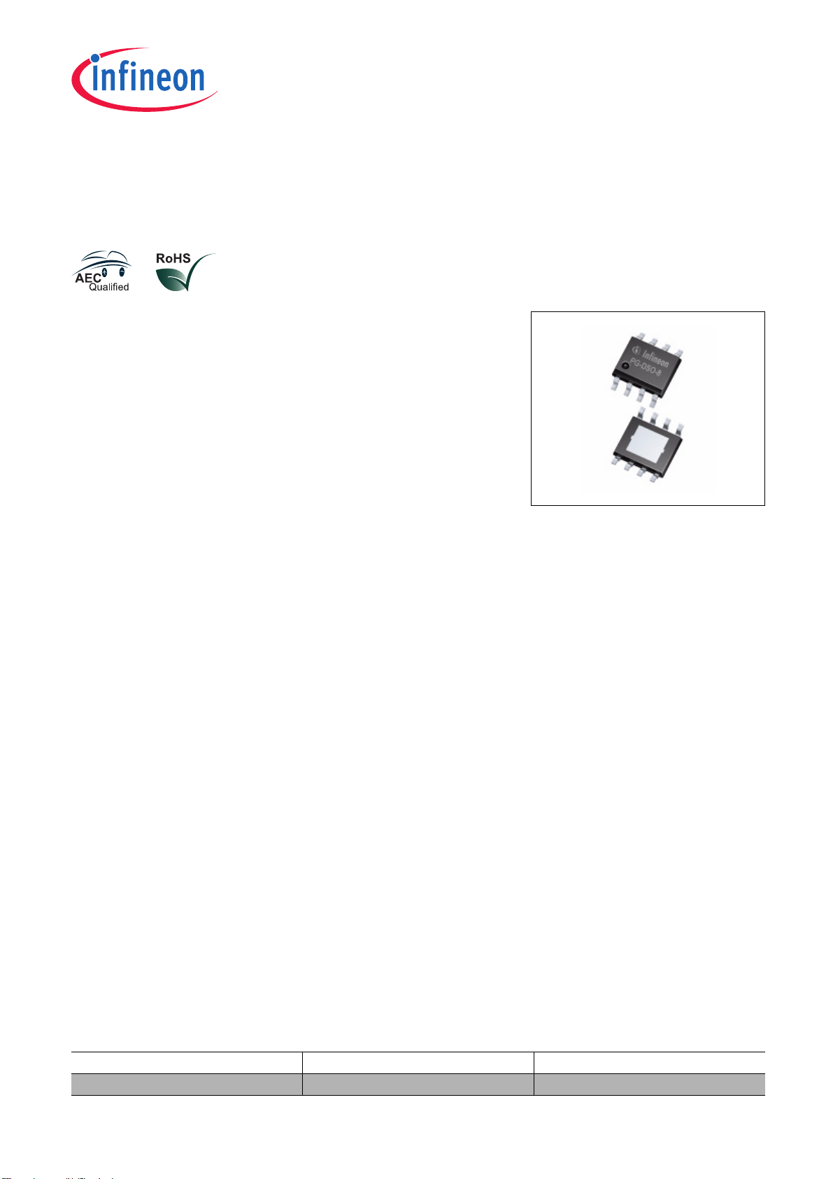
TLE4263-2ES
PG-DSO-8 exposed pad
Description
TLE4263-2ES is a monolithic integrated very low dropout voltage regulator in a SMD package PG-DSO-8 exposed
pad, especially designed for automotive applications. An input voltage up to 45 V is regulated to an output voltage
of 5.0 V. The component is able to drive loads up to 180 mA. The IC is short-circuit proof by the implemented
current limitation and has an integrated overtemperature shutdown.
It additionally provides features like power-on and undervoltage reset with adjustable reset threshold, a watchdog
circuit for monitoring a connected microcontroller and an inhibit input for enabling or disabling the component.
The reset output RO is set to “low” in case the output voltage falls below the reset switching threshold
threshold can be decreased down to 3.5 V by an external resistor divider. The power-on reset delay time can be
programmed by the external delay capacitor
The watchdog circuit provides a monitoring function for microcontrollers: At missing pulses on the watchdog’s
input W the reset output RO is set to “low”. The trigger time for the watchdog pulses can be set by the external
capacitor
The IC can be switched off by the inhibit input, reducing the current consumption to typically 0 µA.
Type Package Marking
TLE4263-2ES PG-DSO-8 exposed pad 4263-2
Data Sheet 2 Rev. 1.0, 2008-04-21
C
.
D
C
.
D
V
. This
Q,rt

TLE4263-2ES
Dimensioning Information on External Components
The input capacitor
for the stability of the control loop. Stability is guaranteed at values ≥ 22 µF and an ESR of ≤ 3 Ω within the
operating temperature range. For small tolerances of the reset delay the capacitance’s spread of the delay
capacitor
Circuit Description
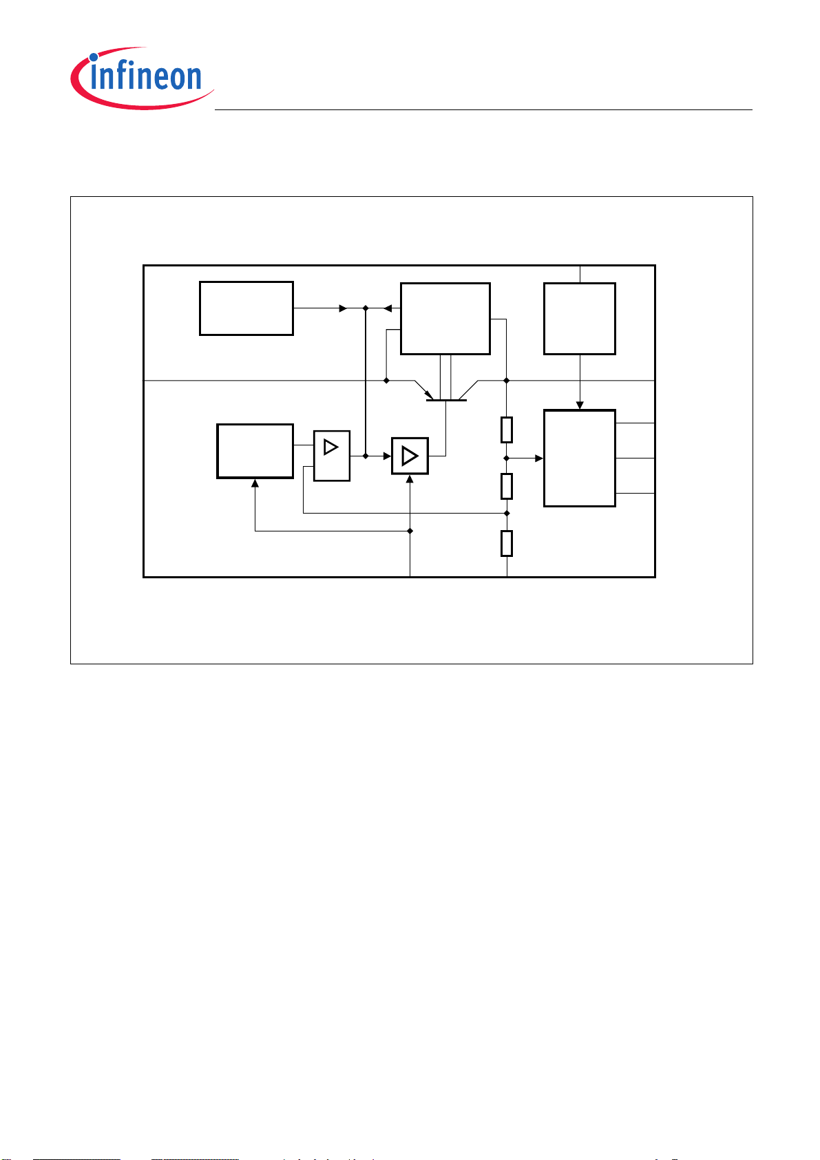
The control amplifier compares a reference voltage to a voltage that is proportional to the output voltage and drives
the base of the series transistor via a buffer. Saturation control as a function of the load current prevents any
oversaturation of the power element. The component also has a number of internal circuits for protection against:
• Overload
• Overtemperature
• Reverse polarity
In case the externally scaled down output voltage at the reset adjust input falls below 1.35 V, the external reset
delay capacitor
threshold
the reset threshold input is connected to GND, reset is triggered at an output voltage of typically 4.65 V.
C
and its temperature coefficient should be taken into consideration.
D
V
DRL
C
is recommended for compensation of line influences. The output capacitor CQ is necessary
I
C
is discharged by the reset generator. When the voltage of the capacitor reaches the lower
D
, a reset signal occurs at the reset output and is held until the upper threshold VDU is exceeded. If
Overview
Data Sheet 3 Rev. 1.0, 2008-04-21
TLE4263-2ES
2 Block Diagram
Temperature
Sensor
Ι Q
Input
Bandgap
Reference
Control
Amplifier
Saturation
Control and
Protection
Circuit
Buffer
W
Watchdog
Reset
Generator
Block Diagram
Output
Reset
D
Delay
RO
Reset
Output
RADJ
Reset
Threshold
Figure 1 Block Diagram
INH
Inhibit
GND
GND
AEB03068
Data Sheet 4 Rev. 1.0, 2008-04-21
TLE4263-2ES
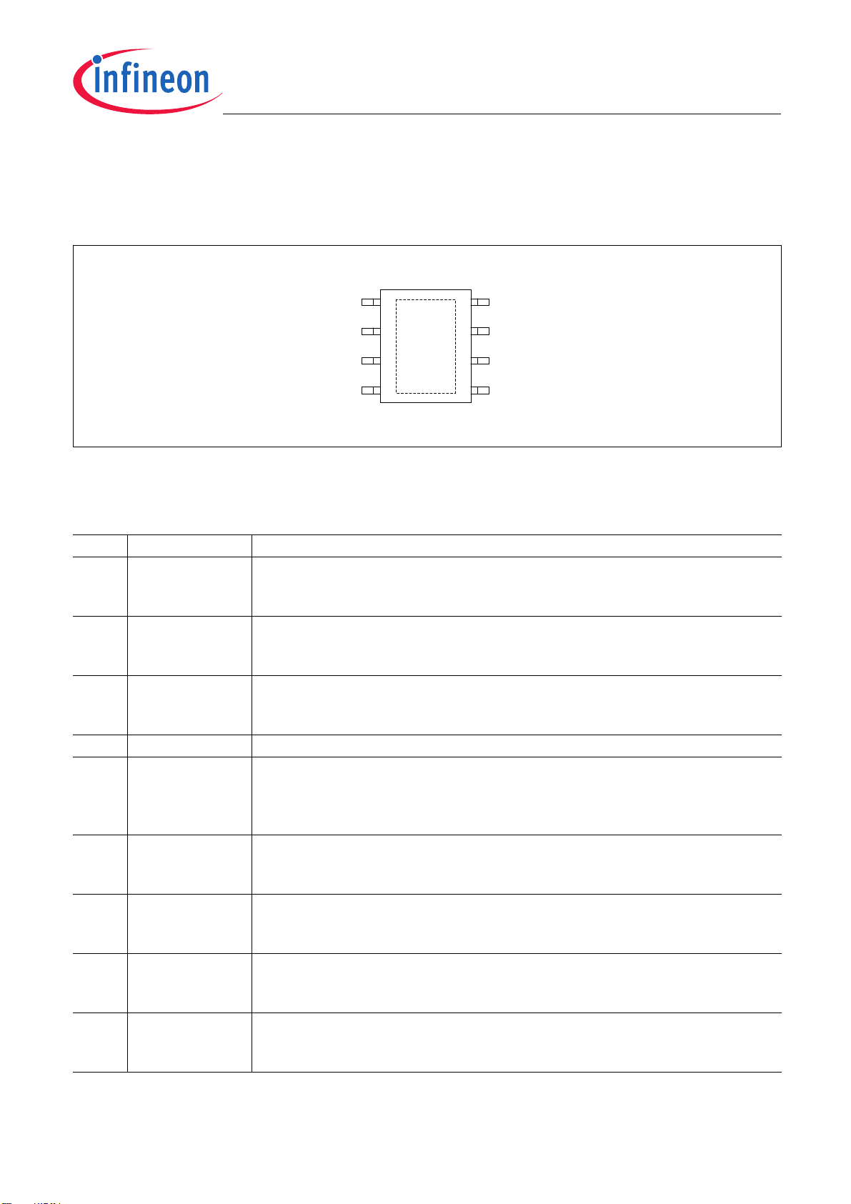
3 Pin Configuration
3.1 Pin Assignment
,
,1+
52
*1'
Figure 2 Pin Configuration
3.2 Pin Definitions and Functions
Pin Configuration
4
:
5$'-
'
Pin Symbol Function
1I Input
for compensating line influences, a capacitor to GND close to the IC terminals is
recommended
2INH Inhibit
enables/disables the device;
connect to I if the this function is not needed
3RO Reset Output
open-collector output connected to the output via an internal 30kΩ pull-up resistor;
leave open if the this function is not needed
4GND Ground
5D Reset Delay Timing
connect a ceramic capacitor to GND for adjusting the reset delay time / watchdog
trigger time;
leave open if this function is not needed
6RADJ Reset Threshold Adjust
connect an external voltage divider to adjust the reset switching threshold;
connect to GND for using internal threshold
7W Watchdog
rising edge triggered input for monitoring a microcontroller;
connect to GND if this function is not needed
8Q Output
block to ground with a capacitor close to the IC terminals with a capacitance value
C ≥ 22 µF, and an ESR ≤ 3 Ω
PAD – Exposed Pad
attach the exposed pad on package bottom to the heatsink area on circuit board;
connect to GND
Data Sheet 5 Rev. 1.0, 2008-04-21
TLE4263-2ES
General Product Characteristics
4 General Product Characteristics
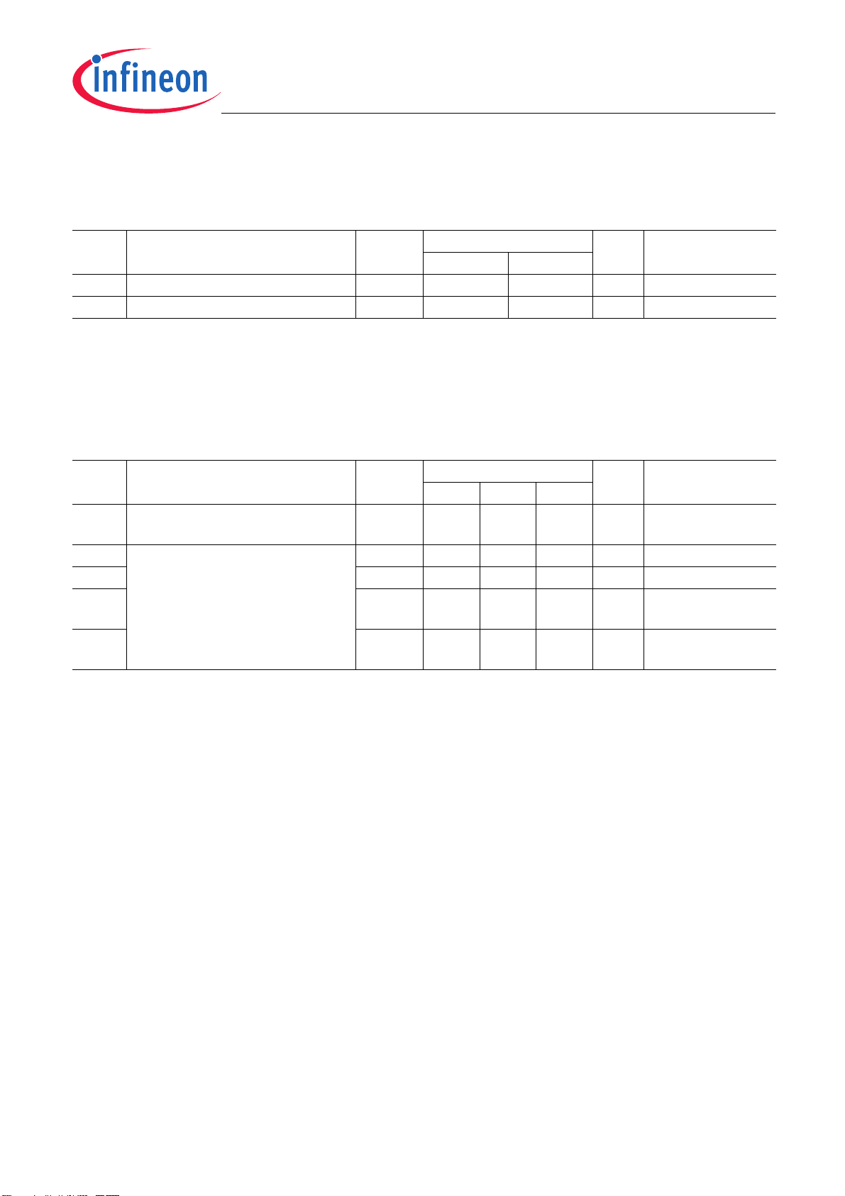
4.1 Absolute Maximum Ratings
Absolute Maximum Ratings
T
= -40 °C to +150 °C; all voltages with respect to ground, positive current flowing into pin
j
(unless otherwise specified)
Pos. Parameter Symbol Limit Values Unit Conditions
Input I, Input INH
4.1.1 Input Voltage
Reset Output RO, Reset Delay D
4.1.2 Voltage
Reset Threshold RADJ
4.1.3 Voltage
Output Q
4.1.4 Voltage
Watchdog W
4.1.5 Voltage
Temperature
4.1.6 Junction Temperature
4.1.7 Storage Temperature
ESD Susceptibility
4.1.8 Human Body Model (HBM)
4.1.9 Charged Device Model (CDM)
1) not subject to production test, specified by design
2) ESD HBM Test according JEDEC JESD22-A114
3) ESD CDM Test according AEC/ESDA ESD-STM5.3.1-1999
1)
Min. Max.
V
, V
I
INH
V
, V
R
V
RADJ
V
Q
V
W
T
j
T
stg
2)
3)
Voltage - 2 kV –
Voltage - 1 kV –
-42 45 V –
-0.3 42 V –
D
-0.3 6 V –
-0.3 7 V –
-0.3 6 V –
–150°C–
-50 150 °C–
Note: Stresses above the ones listed here may cause permanent damage to the device. Exposure to absolute
maximum rating conditions for extended periods may affect device reliability.
Note: Integrated protection functions are designed to prevent IC destruction under fault conditions described in the
data sheet. Fault conditions are considered as “outside” normal operating range. Protection functions are
not designed for continuous repetitive operation.
Data Sheet 6 Rev. 1.0, 2008-04-21
TLE4263-2ES
General Product Characteristics
4.2 Functional Range
Pos. Parameter Symbol Limit Values Unit Conditions
Min. Max.
4.2.1 Input Voltage
4.2.2 Junction Temperature
V
I
T
j
5.5 45 V –
-40 150 °C–
Note: Within the functional range the IC operates as described in the circuit description. The electrical
characteristics are specified within the conditions given in the related electrical characteristics table.
4.3 Thermal Resistance
Pos. Parameter Symbol Limit Values Unit Conditions
Min. Typ. Max.
4.3.1 Junction to Case
4.3.2 Junction to Ambient
4.3.3 R
4.3.4 R
4.3.5 R
1) Not subject to production test, specified by design.
2) Specified R
(Chip+Package) was simulated on a 76.2 x 114.3 x 1.5 mm³ board with 2 inner copper layers (2 x 70µm Cu, 2 x 35µm Cu).
Where applicable a thermal via array under the exposed pad contacted the first inner copper layer.
3) Specified R
(Chip+Package) was simulated on a 76.2 × 114.3 × 1.5 mm
value is according to Jedec JESD51-2,-5,-7 at natural convection on FR4 2s2p board; The Product
thJA
value is according to Jedec JESD 51-3 at natural convection on FR4 1s0p board; The Product
thJA
1)
R
thJC
– 10 – K/W measured to
exposed pad
1)
R
thJA
thJA
thJA
thJA
–45–K/W
– 153 – K/W footprint only
– 64 – K/W 300 mm² heatsink
– 55 – K/W 600 mm² heatsink
3
board with 1 copper layer (1 x 70µm Cu).
2)
area
area
3)
3)
3)
Data Sheet 7 Rev. 1.0, 2008-04-21

TLE4263-2ES
Electrical Characteristics
5 Electrical Characteristics
5.1 Voltage Regulator
Electrical Characteristics Voltage Regulator
V
= 13.5 V, -40 °C ≤ Tj ≤150 °C, V
I
(unless otherwise specified)
Pos. Parameter Symbol Limit Values Unit Conditions
5.1.1 Output Voltage
5.1.2 Output Voltage
5.1.3 Output Current Limitation
5.1.4 Dropout voltage
5.1.5 Load regulation ∆V
5.1.6 Line regulation ∆
5.1.7 Power Supply Ripple
Rejection
1) Drop voltage = Vi - VQ (measured when the output voltage has dropped 100 mV from the nominal value obtained at 6 V
input).
2) Not subject to production test, specified by design.
2)
> 3.6 V; all voltages with respect to ground, positive current flowing into pin
INH
Min. Typ. Max.
V
Q
V
Q
I
Q,max
V
dr
Q,lo
V
Q.li
PSRR –54–dBf
4.90 5.00 5.10 V 5 mA ≤ IQ ≤ 150 mA;
6 V ≤
V
≤ 28 V
I
4.90 5.00 5.10 V 6 V ≤ VI ≤ 32 V;
I
= 100 mA;
Q
T
= 100 °C
j
180 250 400 mA VQ=4.8V
–0.350.60VIQ = 150 mA
1)
––25mVIQ = 5 mA to 150 mA
–325mVVI = 6 V to 28 V;
I
= 150 mA
Q
= 100 Hz;
r
V
= 0.5 Vpp
r
Data Sheet 8 Rev. 1.0, 2008-04-21

TLE4263-2ES
5.2 Typical Performance Characteristics Voltage Regulator
Output Voltage VQ versus
Junction Temperature
T
5.2
V
V
Q
5.1
V
5.0
4.9
4.8
4.7
J
= 13.5 V
I
AED01090
Output Current
Input Voltage
300
mA
Ι
Q
250
200
150
100
50
I
Q
V
I
T
= 25 C
j
versus
Electrical Characteristics
AED01091
4.6
-40 04080120 ˚C 160
T
j
Power Supply Ripple Rejection PSRR versus
ripple frequency
3655
>G%@
f
r
P$
,
4
P$
,
4
P$
,
4
9
9
ULSSOH
9
9
,
)WDQWDOXP
&
4
&
7
M
N N
N
B3655B)69*
>+]@
I
0
100
20
30
40
V
V
Ι
Output Capacitor Series Resistor ESR(C
Output Current
100
ESR
CQ
[Ω]
I
Q
2_ ESR -IQ .VSD
CQ = 22 µF
= -40...150 °C
T
j
10
1
Stable
Region
0.1
0.01
0
50
100
I
50
) versus
Q
150
[mA]
Q
Data Sheet 9 Rev. 1.0, 2008-04-21

TLE4263-2ES
Dropout Voltage
Output Current
800
mV
V
dr
700
600
500
400
300
200
100
V
dr
I
Q
T
= 125 ˚C
j
versus
25 ˚C
AED03060_4263
Output Voltage VQ versus
Input Voltage
V
I
12
V
V
Q
10
8
6
4
2
Electrical Characteristics
AED01097
R
= 25
Ω
L
0
0
50 100 150 200 300
mA
0
I
Q
0
2
68
4
10
V
V
Ι
Data Sheet 10 Rev. 1.0, 2008-04-21

TLE4263-2ES
Electrical Characteristics
5.3 Current Consumption
Electrical Characteristics Voltage Regulator
V
= 13.5 V, -40 °C ≤ Tj ≤150 °C, V
I
> 3.6 V; all voltages with respect to ground, positive current flowing into pin
INH
(unless otherwise specified)
Pos. Parameter Symbol Limit Values Unit Conditions
Min. Typ. Max.
5.3.1 Current Consumption;
I
5.3.2 – 900 1300 µA
= II - I
q
Q
5.3.3 – 10 18 mA
5.3.4 – 15 24 mA
I
q
–010µA V
= 0 V; Tj ≤ 115 °C
INH
I
= 0 mA
Q
I
= 150 mA
Q
I
= 150 mA;
Q
V
= 4.5 V
I
5.4 Typical Performance Characteristics Current Consumption
Current Consumption
Input Voltage
V
I
30
mA
Ι
q
25
I
versus
q
AED01096
Current Consumption Iq versus
Output Current
32
mA
I
q
28
I
Q
24
AED03061
20
15
10
R
L
= 25
Ω
5
0
20010
30
40
V
50
V
Ι
20
16
12
V
= 13.5 V
I
8
4
0
0
50 100 150 200 300
mA
I
Q
Data Sheet 11 Rev. 1.0, 2008-04-21

TLE4263-2ES
Electrical Characteristics
5.5 Inhibit Function
Electrical Characteristics Voltage Regulator
V
= 13.5 V, -40 °C ≤ Tj ≤150 °C, all voltages with respect to ground, positive current flowing into pin
I
(unless otherwise specified)
Pos. Parameter Symbol Limit Values Unit Conditions
Min. Typ. Max.
5.5.1 Switching Voltage
5.5.2 Turn-OFF Voltage
5.5.3 Inhibit Input Current
V
INH,ON
V
INH,OFF
I
INH
3.6 – – V IC turned on
– – 0.8 V IC turned off
51027µA V
INH
= 5 V
5.6 Typical Performance Characteristics Inhibit
Inhibit Input Current
Junction Temperature
16
µA
I
INH
14
I
INH
T
versus
j
AED03063
12
10
V
= 5 V
INH
8
6
4
2
0
80-40
400
160˚C120
T
j
Data Sheet 12 Rev. 1.0, 2008-04-21

TLE4263-2ES
Electrical Characteristics
5.7 Reset Function
Electrical Characteristics Reset Function
V
= 13.5 V, -40 °C ≤ Tj ≤ 150 °C, V
I
(unless otherwise specified)
Pos. Parameter Symbol Limit Values Unit Conditions
Output Undervoltage Reset
5.7.1 Default Output Undervoltage Reset
Switching Thresholds
Output Undervoltage Reset Threshold Adjustment
5.7.2 Reset Adjust
Switching Threshold
5.7.3 Reset Adjustment Range
Reset Output RO
5.7.4 Reset Output Low Voltage
Reset Delay Timing
5.7.5 Power On Reset Delay Time
5.7.6 Saturation Voltage
5.7.7 Upper Delay
Switching Threshold
5.7.8 Lower Delay
Switching Threshold
5.7.9 Delay Capacitor
Charge Current
5.7.10 Reset Reaction Time
1) V
is scaled linearly, in case the Reset Switching Threshold is modified
RT
> 3.6 V; all voltages with respect to ground, positive current flowing into pin
INH
Min. Typ. Max.
V
Q,rt
V
RADJ,th
1)
V
RT,range
V
RO,low
t
rd
V
D,sat
V
DU
V
DRL
I
D,ch
t
rr
4.5 4.65 4.8 V VQ decreasing
1.26 1.36 1.44 V 3.5 V ≤ VQ < 5 V
3.50 – 4.65 V –
–0.10.4VIRO = 1 mA
1.3 2.8 4.1 ms CD = 100 nF
–50110mVVQ < V
R,th
1.40 1.70 2.20 V –
0.20 0.35 0.59 V –
40 60 88 µA–
0.5 1.2 4 µs CD = 100 nF
Note: The reset output is low within the range VQ = 1 V to V
Q,rt
Data Sheet 13 Rev. 1.0, 2008-04-21

TLE4263-2ES
5.8 Typical Performance Characteristics Reset
Undervoltage Reset Adjust Threshold V
versus Junction Temperature T
1.6
V
V
RADJ
1.4
1.2
1.0
0.8
0.6
0.4
j
AED01088
RT
Undervoltage Reset Adjust
Threshold
V
RADJ
1.6
1.4
1.2
1.0
0.8
0.6
0.4
V
RADJ,th
V
Electrical Characteristics
versus Output Voltage V
AED01098_4263
= 13.5 V
V
Ι
Q
0.2
0
-40 04080120 ˚C 160
Timing Threshold Voltage VDU and V
versus Temperature
3.2
V
V
V
2.8
2.4
2.0
1.6
1.2
0.8
0.4
= 13.5 V
I
V
DU
V
DRL
T
j
DRL
AED03062
0.2
0
0
1
3
2
5
4
V
V
Q
0
-40
04080120 160˚C
T
j
Data Sheet 14 Rev. 1.0, 2008-04-21

TLE4263-2ES
Electrical Characteristics
5.9 Watchdog Function
Electrical Characteristics Watchdog Function
V
= 13.5 V, -40 °C ≤ Tj ≤ 150 °C, V
I
(unless otherwise specified)
Pos. Parameter Symbol Limit Values Unit Conditions
5.9.1 Discharge Current
5.9.2 Upper Timing Threshold
5.9.3 Lower Timing Threshold
5.9.4 Watchdog Trigger Time T
5.9.5 Watchdog Output Low Time T
5.9.6 Watchdog Period
T
WI,p
= T
WD,L
+ T
WI,tr
> 3.6 V; all voltages with respect to ground, positive current flowing into pin
INH
Min. Typ. Max.
I
D,wd
V
V
T
DU
DWL
WI,tr
WD,L
WI,p
4.40 6.25 9.40 µA VD = 1.0 V
1.40 1.70 2.20 V –
0.20 0.35 0.55 V –
16 22.5 27 ms CD = 100 nF
V
> V
Q
Q,RT
12.13.5msCD = 100 nF
V
> V
Q
Q,RT
17 24.6 30.5 ms CD = 100 nF
V
> V
Q
Q,RT
5.10 Typical Performance Characteristics Watchdog
Charge Current and Discharge Current
versus Temperature
80
A
µ
Ι
70
Ι
V
Ι
V
D
D, ch
= 13.5 V
= 1.5 V
60
50
AED03064
40
30
20
Ι
10
D, dis
0
0-40 40
12080 160
C
T
j
Watchdog Trigger Time
versus Temperature
40
ms
T
WI,tr
35
30
25
20
15
10
5
0
0-40 40
V
= 13.5 V
Ι
C
= 100 nF
D
AED03065_4263
12080 160
C
T
j
Data Sheet 15 Rev. 1.0, 2008-04-21

TLE4263-2ES
Application Information
6 Application Information
Note: The following information is given as a hint for the implementation of the device only and shall not be
regarded as a description or warranty of a certain functionality, condition or quality of the device.
Ι
Ι
1000 F 470 nF
µ µ
V
V
+
Ι
r
V
E
Ι Q
TLE4263-2 ES
Ι
E
Ι
D, ch
C
GND
Ι
GND
D
D
V
C
100 nF
W RADJ
V
V
W
RADJ
Ι
Q
22 F
Ι
ROINH
RD
Ω5.6 k
V
Q
V
RO
V
PSRR = 20 log
r
V
∆
Q, r
AES03070_4263
Figure 3 Application Diagram
Note: This is a very simplified example of an application circuit. The function must be verified in the real application.
Data Sheet 16 Rev. 1.0, 2008-04-21

TLE4263-2ES
d
6.1 Reset
V
I
V
Q
V
Q, rt
1 V
V
D
V
DU
Application Information
t
t
<
t
rr
t
t
rd
V
DRL
t
V
RO
1V
V
RO,l
rd
Thermal
Shutdown
t
rd
Input
Voltage Dip
Figure 4 Reset Timing Diagram
Power-On Reset Delay Time
If the application needs a power-on reset delay time
t
rd
capacitor’s value can be derived from these specified values and the desired power-on delay time:
t
Undervolta ge
rr
t
rd
Spike at
output
Ove r-
load
different from the value given in Item 5.7.5, the delay
t
t
TimingDiagram_Reset.vs
t
rd new,
----------------
C
D
100nF×=
t
rd
Data Sheet 17 Rev. 1.0, 2008-04-21

TLE4263-2ES
Application Information
with
•
C
: capacitance of the delay capacitor to be chosen
D
•
t
: desired power-on reset delay time
rd,new
•
t
: power-on reset delay time specified in this datasheet
rd
For a precise calculation also take the delay capacitor’s tolerance into consideration.
Reset Adjust Function
The undervoltage reset switching threshold can be adjusted according to the application’s needs by connecting
an external voltage divider (
R
ADJ1
, R
) at pin RADJ. For selecting the default threshold connect pin RADJ to
ADJ2
GND.
When dimensioning the voltage divider, take into consideration that there will be an additional current constantly
flowing through the resistors.
With a voltage divider connected, the reset switching threshold
R
ADJ 1,
V
RT new,
-----------------------------------------R
ADJ 2,
R+
ADJ 2,
V
×=
RADJ th,
V
is calculated as follows:
RT,new
(1)
with
•
•
V
RADJ,th
V
: the desired new reset switching threshold
RT,new
R
, R
ADJ1
: reset adjust switching threshold given in “Reset Function” on Page 13
: resistors of the external voltage divider
ADJ2
Data Sheet 18 Rev. 1.0, 2008-04-21

TLE4263-2ES
6.2 Watchdog
V
W
V
D
V
DU
V
DWL
V
RO
No p ositive
V
edge
W
t
WD, L
Application Information
t
t
WI , t r
t
WD, L
T
WI ,p
t
V
RO,l
TimingDiagram_Watchdog.vsd
t
Figure 5 Timing of the Watchdog Function Reset
Watchdog Timing
The period of the watchdog pulses has to be smaller than the minimum watchdog trigger time which is set by the
external reset delay capacitor
T
WI,tr,new
------------------------
C
D
T
WI,tr
100 nF×=
C
. Use the following formula for dimensioning CD:
D
(2)
with
•
C
: capacitance of the delay capacitor to be chosen
D
•T
•T
: desired watchdog trigger time
WI,tr,new
: watchdog trigger time specified in this data sheet
WI,tr
Data Sheet 19 Rev. 1.0, 2008-04-21

TLE4263-2ES
)
7 Package Outlines
1.27
2)
±0.09
0.41
A
8
5
14
B
1)
±0.1
4.9
Index Marking
+0
-0.1
0.1
Stand Off
(1.45)
C
M
0.2 DC A-B
1.7 MAX.
8x
A-BC0.1 2x
0.08
C
Seating Plane
±0.1
3.9
D
Bottom View
0.35 x 45˚
1)
0.64
±0.2
6
±0.2
3
14
85
0.1
+0.06
0.19
±0.25
0.2
±0.2
2.65
Package Outlines
CD2x
MAX.
˚
8
M
D 8x
1) Does not include plastic or metal protrusion of 0.15 max. per side
2) Dambar protrusion shall be maximum 0.1 mm total in excess of lead width
3
JEDEC reference MS-012 variation BA
PG-DSO-8-27-PO V01
Figure 6 PG-DSO-8 exposed pad
Green Product (RoHS compliant)
To meet the world-wide customer requirements for environmentally friendly products and to be compliant with
government regulations the device is available as a green product. Green products are RoHS-Compliant (i.e
Pb-free finish on leads and suitable for Pb-free soldering according to IPC/JEDEC J-STD-020).
You can find all of our packages, sorts of packing and others in our
Infineon Internet Page “Products”: http://www.infineon.com/products.
Dimensions in mm
Data Sheet 20 Rev. 1.0, 2008-04-21

TLE4263-2ES
8 Revision History
Revision Date Changes
1.0 2008-04-21 final version data sheet
Revision History
Data Sheet 21 Rev. 1.0, 2008-04-21

Edition 2008-04-21
Published by
Infineon Technologies AG
81726 Munich, Germany
© 2007 Infineon Technologies AG
All Rights Reserved.
Legal Disclaimer
The information given in this document shall in no event be regarded as a guarantee of conditions or
characteristics. With respect to any examples or hints given herein, any typical values stated herein and/or any
information regarding the application of the device, Infineon Technologies hereby disclaims any and all warranties
and liabilities of any kind, including without limitation, warranties of non-infringement of intellectual property rights
of any third party.
Information
For further information on technology, delivery terms and conditions and prices, please contact the nearest
Infineon Technologies Office (www.infineon.com).
Warnings
Due to technical requirements, components may contain dangerous substances. For information on the types in
question, please contact the nearest Infineon Technologies Office.
Infineon Technologies components may be used in life-support devices or systems only with the express written
approval of Infineon Technologies, if a failure of such components can reasonably be expected to cause the failure
of that life-support device or system or to affect the safety or effectiveness of that device or system. Life support
devices or systems are intended to be implanted in the human body or to support and/or maintain and sustain
and/or protect human life. If they fail, it is reasonable to assume that the health of the user or other persons may
be endangered.
 Loading...